Deep reactive ion etching as a tool for nanostructure fabrication · 2009-06-01 · conventional...
7
Deep reactive ion etching as a tool for nanostructure fabrication Y. Q. Fu a Department of Engineering, University of Cambridge, 9 J.J. Thomson Avenue, Cambridge CB3 0FA, United Kingdom and Department of Mechanical Engineering, School of Engineering and Physical Sciences, Heriot Watt University, Edinburgh EH14 4AS, United Kingdom A. Colli Nokia Research Centre Cambridge, c/o Nanoscience Centre, Cambridge CB3 0FF, United Kingdom A. Fasoli Department of Engineering, University of Cambridge, 9 J.J. Thomson Avenue, Cambridge CB3 0FA, United Kingdom J. K. Luo Department of Engineering, University of Cambridge, 9 J.J. Thomson Avenue, Cambridge CB3 0FA, United Kingdom and Centre for Material Research and Innovation, University of Bolton, Deane Road, Bolton BL3 5AB, United Kingdom A. J. Flewitt, A. C. Ferrari, and W. I. Milne Department of Engineering, University of Cambridge, 9 J.J. Thomson Avenue, Cambridge CB3 0FA, United Kingdom Received 29 September 2008; accepted 8 December 2008; published 27 May 2009 Deep reactive ion etching DRIE is investigated as a tool for the realization of nanostructures and architectures, including nanopillars, silicon nanowires or carbon nanotubes on Si nanopillars, nanowalls, and nanonetworks. The potential of combining top-down fabrication methods with the bottom-up synthesis of one-dimensional nanocomponents is assessed. The field-emission properties of carbon nanotubes/Si pillars hybrid structures are measured, as well as the transport properties of large-area nanowires obtained via nanowire lithography. The potential of DRIE for the fabrication of three-dimensional nanostructures is also revealed. © 2009 American Vacuum Society. DOI: 10.1116/1.3065991 I. INTRODUCTION Nanosize vertical silicon structures with high aspect ratio are crucial for many applications, such as photonics, optical waveguides, microfluidics, DNA separation, heat dissipation, etc. 1–3 Two approaches are generally followed to fabricate them. The first relies on bottom-up methods, the most popu- lar being the catalyst-assisted growth of vertical silicon nanowires SiNWs. 4,5 The second relies on top-down manu- facturing, namely, high-aspect-ratio anisotropic etching of silicon wafers. 4,5 So far, these two approaches have pro- gressed on two parallel tracks, and their independent devel- opment could be seen as a competition to set a single nano- fabrication standard. Amongst top-down methods, deep reaction ion etching DRIE is regarded as a powerful method to fabricate vertical silicon structures or pillars. 2,3,6,7 The DRIE process is a key silicon micromachining technique, and in microelectrome- chanical system MEMS device fabrication, anisotropic DRIE of silicon is a mature process technology that is used for creating three-dimensional 3D mechanical structures. 8,9 Recently, DRIE has been also successfully applied to through-wafer etching for advanced packaging. 10 A typical DRIE process involves the use of a high-density plasma and comprises a sequence of alternating steps no more than a few seconds long of silicon etching and polymer deposition to protect the already-carved features from further lateral etching. As cycles go on, the micromachining proceeds via a series of “bites” into the silicon, each on the order of 0.5–5.0 m deep. These are usually called “scalloping” or “ripple,” see Figs. 1a and 1b. 8–10 For nanostructure etch- ing, however, scalloping can become a serious problem. 6,7 As feature size and scallop size become comparable, the process conditions have to be adjusted to minimize the ripple, in order to ensure smooth sidewalls at the nanoscale. This can be achieved by optimizing source power, bias power, gas flow rate, flow cycle time, substrate temperature, and cham- ber pressure. In this study, we illustrate an optimized DRIE process for the fabrication of smooth silicon nanostructures, including nanopillars, nanowires, and nanowalls. We also show that we can favorably exploit and control the scalloping effect to realize novel three-dimensional nanostructures. We then de- vise advanced mask-engineering solutions that allow us to combine the advantages of both top-down and bottom-up fabrication methods. These include the possibility of using etching masks for DRIE that can later catalyse the growth of individual or multiple NWs or nanotubes. Further, we show that bottom-up nanostructures themselves such as nanopar- ticles, NWs, or nanospheres can be used as etching masks a Author to whom correspondence should be addressed; electronic mail: [email protected] 1520 1520 J. Vac. Sci. Technol. B 27„3…, May/Jun 2009 1071-1023/2009/27„3…/1520/7/$25.00 ©2009 American Vacuum Society
Transcript of Deep reactive ion etching as a tool for nanostructure fabrication · 2009-06-01 · conventional...
Deep reactive ion etching as a tool for nanostructure fabricationY. Q. Fua�
Department of Engineering, University of Cambridge, 9 J.J. Thomson Avenue, Cambridge CB3 0FA,United Kingdom and Department of Mechanical Engineering, School of Engineering and Physical Sciences,Heriot Watt University, Edinburgh EH14 4AS, United Kingdom
A. ColliNokia Research Centre Cambridge, c/o Nanoscience Centre, Cambridge CB3 0FF, United Kingdom
A. FasoliDepartment of Engineering, University of Cambridge, 9 J.J. Thomson Avenue, Cambridge CB3 0FA,United Kingdom
J. K. LuoDepartment of Engineering, University of Cambridge, 9 J.J. Thomson Avenue, Cambridge CB3 0FA,United Kingdom and Centre for Material Research and Innovation, University of Bolton, Deane Road,Bolton BL3 5AB, United Kingdom
A. J. Flewitt, A. C. Ferrari, and W. I. MilneDepartment of Engineering, University of Cambridge, 9 J.J. Thomson Avenue, Cambridge CB3 0FA,United Kingdom
�Received 29 September 2008; accepted 8 December 2008; published 27 May 2009�
Deep reactive ion etching �DRIE� is investigated as a tool for the realization of nanostructures andarchitectures, including nanopillars, silicon nanowires or carbon nanotubes on Si nanopillars,nanowalls, and nanonetworks. The potential of combining top-down fabrication methods with thebottom-up synthesis of one-dimensional nanocomponents is assessed. The field-emission propertiesof carbon nanotubes/Si pillars hybrid structures are measured, as well as the transport properties oflarge-area nanowires obtained via nanowire lithography. The potential of DRIE for the fabricationof three-dimensional nanostructures is also revealed. © 2009 American Vacuum Society.
�DOI: 10.1116/1.3065991�I. INTRODUCTION
Nanosize vertical silicon structures with high aspect ratioare crucial for many applications, such as photonics, opticalwaveguides, microfluidics, DNA separation, heat dissipation,etc.1–3 Two approaches are generally followed to fabricatethem. The first relies on bottom-up methods, the most popu-lar being the catalyst-assisted growth of vertical siliconnanowires �SiNWs�.4,5 The second relies on top-down manu-facturing, namely, high-aspect-ratio anisotropic etching ofsilicon wafers.4,5 So far, these two approaches have pro-gressed on two parallel tracks, and their independent devel-opment could be seen as a competition to set a single nano-fabrication standard.
Amongst top-down methods, deep reaction ion etching�DRIE� is regarded as a powerful method to fabricate verticalsilicon structures or pillars.2,3,6,7 The DRIE process is a keysilicon micromachining technique, and in microelectrome-chanical system �MEMS� device fabrication, anisotropicDRIE of silicon is a mature process technology that is usedfor creating three-dimensional �3D� mechanical structures.8,9
Recently, DRIE has been also successfully applied tothrough-wafer etching for advanced packaging.10 A typicalDRIE process involves the use of a high-density plasma and
a�Author to whom correspondence should be addressed; electronic mail:
[email protected]1520 J. Vac. Sci. Technol. B 27„3…, May/Jun 2009 1071-1023/2009
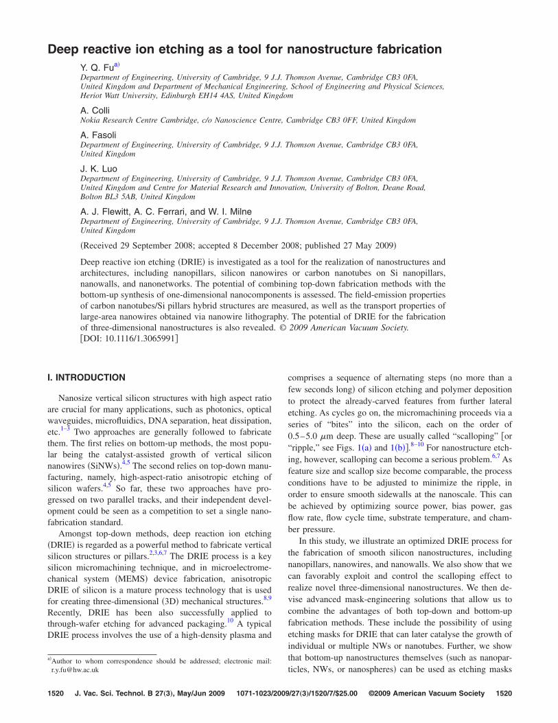
comprises a sequence of alternating steps �no more than afew seconds long� of silicon etching and polymer depositionto protect the already-carved features from further lateraletching. As cycles go on, the micromachining proceeds via aseries of “bites” into the silicon, each on the order of0.5–5.0 �m deep. These are usually called “scalloping” �or“ripple,” see Figs. 1�a� and 1�b��.8–10 For nanostructure etch-ing, however, scalloping can become a serious problem.6,7 Asfeature size and scallop size become comparable, the processconditions have to be adjusted to minimize the ripple, inorder to ensure smooth sidewalls at the nanoscale. This canbe achieved by optimizing source power, bias power, gasflow rate, flow cycle time, substrate temperature, and cham-ber pressure.
In this study, we illustrate an optimized DRIE process forthe fabrication of smooth silicon nanostructures, includingnanopillars, nanowires, and nanowalls. We also show that wecan favorably exploit and control the scalloping effect torealize novel three-dimensional nanostructures. We then de-vise advanced mask-engineering solutions that allow us tocombine the advantages of both top-down and bottom-upfabrication methods. These include the possibility of usingetching masks for DRIE that can later catalyse the growth ofindividual or multiple NWs or nanotubes. Further, we showthat bottom-up nanostructures themselves �such as nanopar-
ticles, NWs, or nanospheres� can be used as etching masks1520/27„3…/1520/7/$25.00 ©2009 American Vacuum Society
1521 Fu et al.: Deep reactive ion etching as a tool for nanostructure fabrication 1521
for top-down micromachining.11–13 These hybrid solutionshighlight a broad fabrication potential, where lithography-free nanostructures organized by self-assembly merge withwell-established and commercially compatible top-downprocessing methods.
II. EXPERIMENTAL DETAILS
Dry etching of silicon wafers was carried out in an induc-tively coupled plasma reactive ion etching �ICP-RIE� system�Alcatel, AMS100�. The coil rf power was varied from500 to 800 W, while the platen power was set to 50 W. Al-ternated etching/passivation cycles with gas flows of SF6
�250 SCCM �SCCM denotes cubic centimeter per minute atSTP� and 1 s�, C4F8 �200 SCCM and 1 s�, and O2
�100 SCCM and 0.5 s� were used with a three-step process�etching silicon, passivation, and etching the passivationlayer�. The substrate temperature was kept at 0 °C by meansof a helium-cooled sample holder. Samples were examined
FIG. 1. �a� Illustration of two alternative DRIE processes of etching andpassivation; �b� SEM micrograph of a typical scalloping pattern.
by scanning electron microscopy �SEM� to investigate the
JVST B - Microelectronics and Nanometer Structures
relationship between etch rate and aspect ratio of the result-ing structures.
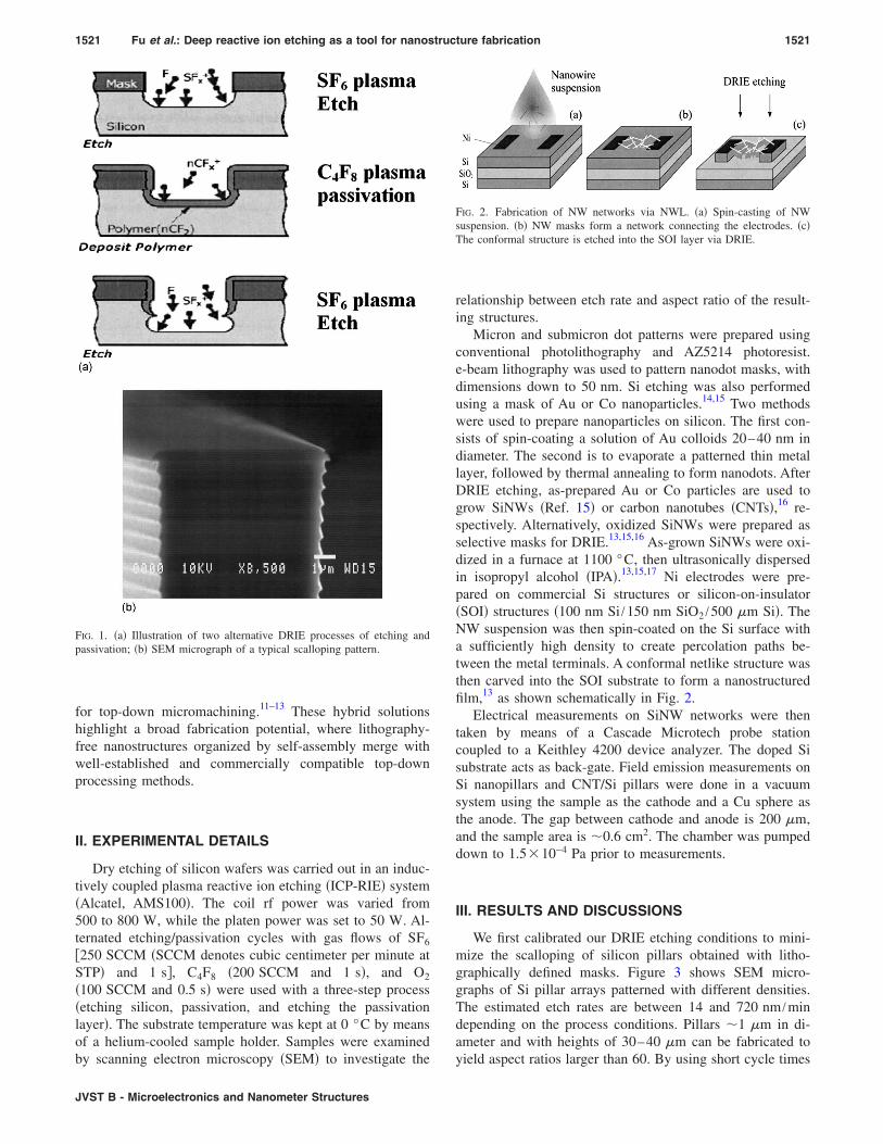
Micron and submicron dot patterns were prepared usingconventional photolithography and AZ5214 photoresist.e-beam lithography was used to pattern nanodot masks, withdimensions down to 50 nm. Si etching was also performedusing a mask of Au or Co nanoparticles.14,15 Two methodswere used to prepare nanoparticles on silicon. The first con-sists of spin-coating a solution of Au colloids 20–40 nm indiameter. The second is to evaporate a patterned thin metallayer, followed by thermal annealing to form nanodots. AfterDRIE etching, as-prepared Au or Co particles are used togrow SiNWs �Ref. 15� or carbon nanotubes �CNTs�,16 re-spectively. Alternatively, oxidized SiNWs were prepared asselective masks for DRIE.13,15,16 As-grown SiNWs were oxi-dized in a furnace at 1100 °C, then ultrasonically dispersedin isopropyl alcohol �IPA�.13,15,17 Ni electrodes were pre-pared on commercial Si structures or silicon-on-insulator�SOI� structures �100 nm Si /150 nm SiO2 /500 �m Si�. TheNW suspension was then spin-coated on the Si surface witha sufficiently high density to create percolation paths be-tween the metal terminals. A conformal netlike structure wasthen carved into the SOI substrate to form a nanostructuredfilm,13 as shown schematically in Fig. 2.
Electrical measurements on SiNW networks were thentaken by means of a Cascade Microtech probe stationcoupled to a Keithley 4200 device analyzer. The doped Sisubstrate acts as back-gate. Field emission measurements onSi nanopillars and CNT/Si pillars were done in a vacuumsystem using the sample as the cathode and a Cu sphere asthe anode. The gap between cathode and anode is 200 �m,and the sample area is �0.6 cm2. The chamber was pumpeddown to 1.5�10−4 Pa prior to measurements.
III. RESULTS AND DISCUSSIONS
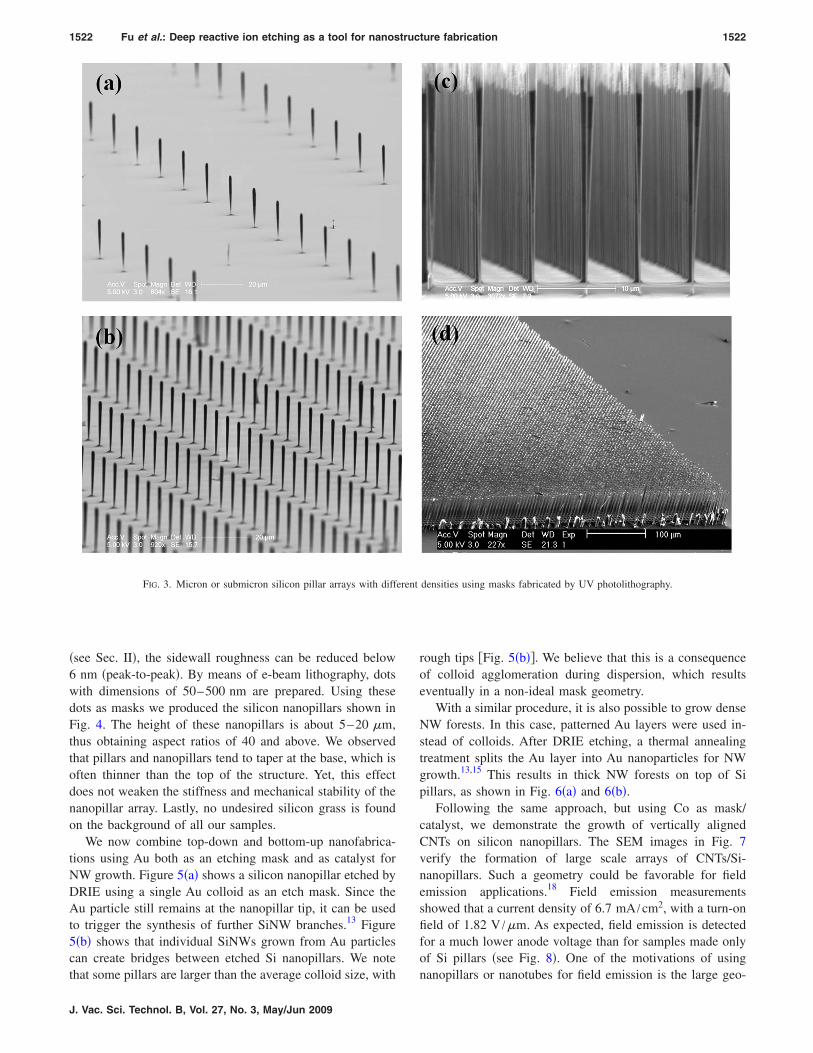
We first calibrated our DRIE etching conditions to mini-mize the scalloping of silicon pillars obtained with litho-graphically defined masks. Figure 3 shows SEM micro-graphs of Si pillar arrays patterned with different densities.The estimated etch rates are between 14 and 720 nm /mindepending on the process conditions. Pillars �1 �m in di-ameter and with heights of 30–40 �m can be fabricated to
FIG. 2. Fabrication of NW networks via NWL. �a� Spin-casting of NWsuspension. �b� NW masks form a network connecting the electrodes. �c�The conformal structure is etched into the SOI layer via DRIE.
yield aspect ratios larger than 60. By using short cycle times
erent
1522 Fu et al.: Deep reactive ion etching as a tool for nanostructure fabrication 1522
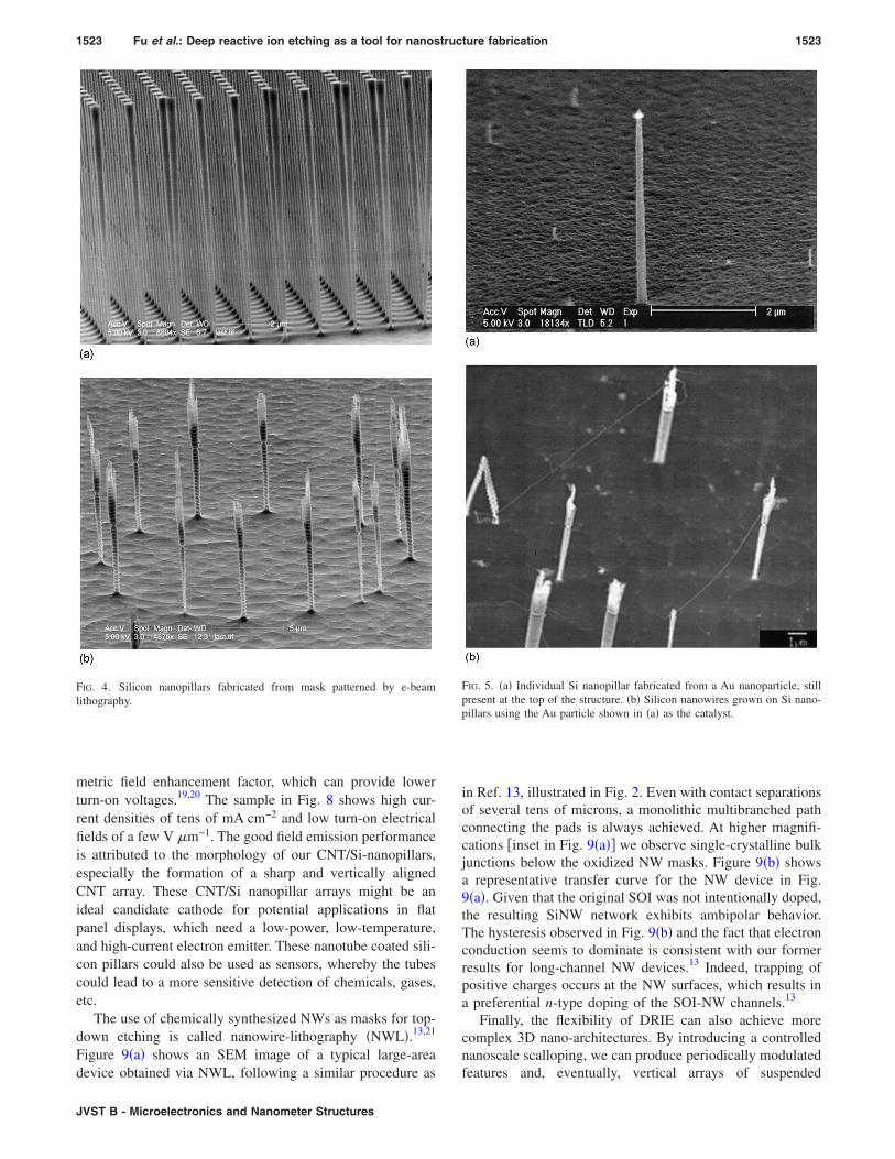
�see Sec. II�, the sidewall roughness can be reduced below6 nm �peak-to-peak�. By means of e-beam lithography, dotswith dimensions of 50–500 nm are prepared. Using thesedots as masks we produced the silicon nanopillars shown inFig. 4. The height of these nanopillars is about 5–20 �m,thus obtaining aspect ratios of 40 and above. We observedthat pillars and nanopillars tend to taper at the base, which isoften thinner than the top of the structure. Yet, this effectdoes not weaken the stiffness and mechanical stability of thenanopillar array. Lastly, no undesired silicon grass is foundon the background of all our samples.
We now combine top-down and bottom-up nanofabrica-tions using Au both as an etching mask and as catalyst forNW growth. Figure 5�a� shows a silicon nanopillar etched byDRIE using a single Au colloid as an etch mask. Since theAu particle still remains at the nanopillar tip, it can be usedto trigger the synthesis of further SiNW branches.13 Figure5�b� shows that individual SiNWs grown from Au particlescan create bridges between etched Si nanopillars. We note
FIG. 3. Micron or submicron silicon pillar arrays with diff
that some pillars are larger than the average colloid size, with
J. Vac. Sci. Technol. B, Vol. 27, No. 3, May/Jun 2009
rough tips �Fig. 5�b��. We believe that this is a consequenceof colloid agglomeration during dispersion, which resultseventually in a non-ideal mask geometry.
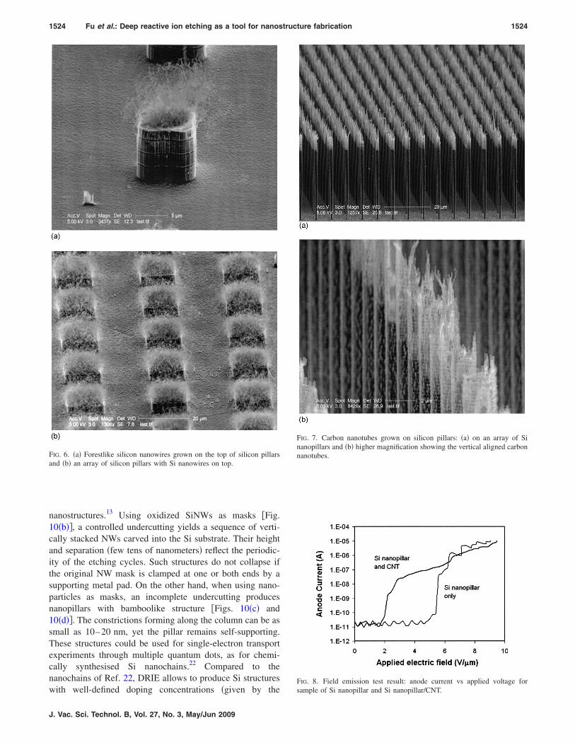
With a similar procedure, it is also possible to grow denseNW forests. In this case, patterned Au layers were used in-stead of colloids. After DRIE etching, a thermal annealingtreatment splits the Au layer into Au nanoparticles for NWgrowth.13,15 This results in thick NW forests on top of Sipillars, as shown in Fig. 6�a� and 6�b�.
Following the same approach, but using Co as mask/catalyst, we demonstrate the growth of vertically alignedCNTs on silicon nanopillars. The SEM images in Fig. 7verify the formation of large scale arrays of CNTs/Si-nanopillars. Such a geometry could be favorable for fieldemission applications.18 Field emission measurementsshowed that a current density of 6.7 mA /cm2, with a turn-onfield of 1.82 V /�m. As expected, field emission is detectedfor a much lower anode voltage than for samples made onlyof Si pillars �see Fig. 8�. One of the motivations of using
densities using masks fabricated by UV photolithography.
nanopillars or nanotubes for field emission is the large geo-
1523 Fu et al.: Deep reactive ion etching as a tool for nanostructure fabrication 1523
metric field enhancement factor, which can provide lowerturn-on voltages.19,20 The sample in Fig. 8 shows high cur-rent densities of tens of mA cm−2 and low turn-on electricalfields of a few V �m−1. The good field emission performanceis attributed to the morphology of our CNT/Si-nanopillars,especially the formation of a sharp and vertically alignedCNT array. These CNT/Si nanopillar arrays might be anideal candidate cathode for potential applications in flatpanel displays, which need a low-power, low-temperature,and high-current electron emitter. These nanotube coated sili-con pillars could also be used as sensors, whereby the tubescould lead to a more sensitive detection of chemicals, gases,etc.
The use of chemically synthesized NWs as masks for top-down etching is called nanowire-lithography �NWL�.13,21
Figure 9�a� shows an SEM image of a typical large-area
FIG. 4. Silicon nanopillars fabricated from mask patterned by e-beamlithography.
device obtained via NWL, following a similar procedure as
JVST B - Microelectronics and Nanometer Structures
in Ref. 13, illustrated in Fig. 2. Even with contact separationsof several tens of microns, a monolithic multibranched pathconnecting the pads is always achieved. At higher magnifi-cations �inset in Fig. 9�a�� we observe single-crystalline bulkjunctions below the oxidized NW masks. Figure 9�b� showsa representative transfer curve for the NW device in Fig.9�a�. Given that the original SOI was not intentionally doped,the resulting SiNW network exhibits ambipolar behavior.The hysteresis observed in Fig. 9�b� and the fact that electronconduction seems to dominate is consistent with our formerresults for long-channel NW devices.13 Indeed, trapping ofpositive charges occurs at the NW surfaces, which results ina preferential n-type doping of the SOI-NW channels.13
Finally, the flexibility of DRIE can also achieve morecomplex 3D nano-architectures. By introducing a controllednanoscale scalloping, we can produce periodically modulated
FIG. 5. �a� Individual Si nanopillar fabricated from a Au nanoparticle, stillpresent at the top of the structure. �b� Silicon nanowires grown on Si nano-pillars using the Au particle shown in �a� as the catalyst.
features and, eventually, vertical arrays of suspended
nanotubes.
1524 Fu et al.: Deep reactive ion etching as a tool for nanostructure fabrication 1524
nanostructures.13 Using oxidized SiNWs as masks �Fig.10�b��, a controlled undercutting yields a sequence of verti-cally stacked NWs carved into the Si substrate. Their heightand separation �few tens of nanometers� reflect the periodic-ity of the etching cycles. Such structures do not collapse ifthe original NW mask is clamped at one or both ends by asupporting metal pad. On the other hand, when using nano-particles as masks, an incomplete undercutting producesnanopillars with bamboolike structure �Figs. 10�c� and10�d��. The constrictions forming along the column can be assmall as 10–20 nm, yet the pillar remains self-supporting.These structures could be used for single-electron transportexperiments through multiple quantum dots, as for chemi-cally synthesised Si nanochains.22 Compared to thenanochains of Ref. 22, DRIE allows to produce Si structures
FIG. 6. �a� Forestlike silicon nanowires grown on the top of silicon pillarsand �b� an array of silicon pillars with Si nanowires on top.
with well-defined doping concentrations �given by the
J. Vac. Sci. Technol. B, Vol. 27, No. 3, May/Jun 2009
FIG. 7. Carbon nanotubes grown on silicon pillars: �a� on an array of Sinanopillars and �b� higher magnification showing the vertical aligned carbon
FIG. 8. Field emission test result: anode current vs applied voltage for
sample of Si nanopillar and Si nanopillar/CNT.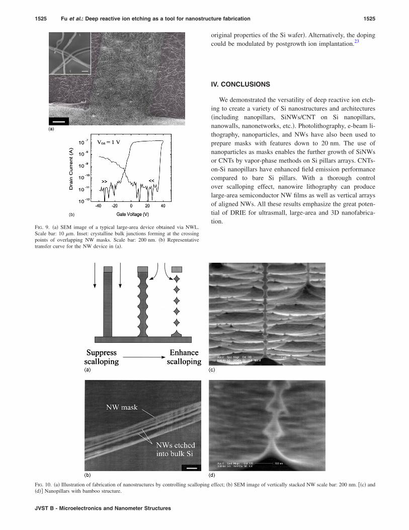
�d�� Nanopillars with bamboo structure.
1525 Fu et al.: Deep reactive ion etching as a tool for nanostructure fabrication 1525
JVST B - Microelectronics and Nanometer Structures
original properties of the Si wafer�. Alternatively, the dopingcould be modulated by postgrowth ion implantation.23
IV. CONCLUSIONS
We demonstrated the versatility of deep reactive ion etch-ing to create a variety of Si nanostructures and architectures�including nanopillars, SiNWs/CNT on Si nanopillars,nanowalls, nanonetworks, etc.�. Photolithography, e-beam li-thography, nanoparticles, and NWs have also been used toprepare masks with features down to 20 nm. The use ofnanoparticles as masks enables the further growth of SiNWsor CNTs by vapor-phase methods on Si pillars arrays. CNTs-on-Si nanopillars have enhanced field emission performancecompared to bare Si pillars. With a thorough controlover scalloping effect, nanowire lithography can producelarge-area semiconductor NW films as well as vertical arraysof aligned NWs. All these results emphasize the great poten-tial of DRIE for ultrasmall, large-area and 3D nanofabrica-tion.
effect; �b� SEM image of vertically stacked NW scale bar: 200 nm. ��c� and
FIG. 9. �a� SEM image of a typical large-area device obtained via NWL.Scale bar: 10 �m. Inset: crystalline bulk junctions forming at the crossingpoints of overlapping NW masks. Scale bar: 200 nm. �b� Representativetransfer curve for the NW device in �a�.
FIG. 10. �a� Illustration of fabrication of nanostructures by controlling scalloping
1526 Fu et al.: Deep reactive ion etching as a tool for nanostructure fabrication 1526
ACKNOWLEDGMENTS
We thank Dr. S. Pisana, Dr. S. P. Ooi, and Dr. X. Z. Wang,for their precious experimental support. One of the authors�A.C.F.� acknowledges funding from the Royal Society andfrom the European Research Council �project NANOPOTS�.One of the authors �Y.Q.F.� would like to acknowledge sup-port from the Royal Society of Edinburgh and CarnegieTrust.
1J. Ohara, K. Kano, and Y. Takeuchi, Sens. Actuators, A 143, 77 �2008�.2Y. Huang, X. Huan, and C. M. Lieber, Small 1, 142 �2005�.3S. H. G. Teo et al., Int. J. Nanosci. 4, 567 �2005�.4A. I. Hochbaum, R. Fan, R. R. He, and P. D. Yang, Nano Lett. 5, 457�2005�.
5L. Schubert, P. Werner, N. D. Zakharov, G. Gerth, F. M. Kolb, L. Long,U. Gosele, and T. Y. Tan, Appl. Phys. Lett. 84, 4968 �2004�.
6L. Sainiemi et al., Nanotechnology 18, 505303 �2007�.7K. J. Morton et al., Nanotechnology 19, 345301 �2008�.8F. Lärmer and A. Schilp, Patent No. DE 4241045, 1996; US 5501893,1996; EP 625285, 1996.
9W. Lang, Mater. Sci. Eng. R. 17, 1 �1996�.10L. M. Lea and C. L. Short, Solid State Technol. 50, 58 �2007�.11W. Li et al., Nanotechnology 19, 135308 �2008�.
J. Vac. Sci. Technol. B, Vol. 27, No. 3, May/Jun 2009
12D. Whang, S. Jin, and C. M. Lieber, Nano Lett. 3, 951 �2003�.13A. Colli, A. Fasoli, S. Pisana, Y. Q. Fu, P. Beecher, W. I. Milne, and A. C.
Ferrari, Nano Lett. 8, 1358 �2008�.14V. Ovchinnikov, A. Malinin, S. Novikov, and C. Tuovinen, Mater. Sci.
Eng., B 69–70, 459 �2000�.15A. Colli, A. Fasoli, P. Beecher, P. Servati, S. Pisana, Y. Q. Fu, A. J.
Flewitt, W. I. Milne, J. Robertson, C. Ducati, S. De Franceschi, S. Hof-mann, and A. C. Ferrari, J. Appl. Phys. 102, 034302 �2007�.
16M. Chhowalla, K. B. K. Teo, C. Ducati, N. L. Rupesinghe, G. A. J.Amaratunga, A. C. Ferrari, D. Roy, J. Robertson, and W. I. Milne, J.Appl. Phys. 90, 5308 �2001�.
17P. Beecher, P. Servati, A. Rozhin, A. Colli, V. Scardaci, S. Pisana, T.Hasan, A. J. Flewitt, J. Robertson, G. W. Hsieh, F. M. Li, A. Nathan, A.C. Ferrari, and W. I. Milne, J. Appl. Phys. 102, 043710 �2007�.
18M. Chhowalla, C. Ducati, N. L. Rupesinghe, K. B. K. Teo, and G. A. J.Amaratunga, Appl. Phys. Lett. 79, 2079 �2001�.
19J. M. Bonard, M. Croci, C. Klinke, R. Kurt, O. Noury, and N. Weiss,Carbon 40, 1715 �2002�.
20W. I. Milne, K. B. K. Teo, G. A. J. Amaratunga, P. Legagneux, L. Gan-gloff, J. P. Schnell, V. Semet, V. T. Binh, and O. Groening, J. Mater.Chem. 14, 933 �2004�.
21D. Whang, S. Jin, and C. M. Lieber, Nano Lett. 3, 951 �2003�.22M. A. Rafiq, H. Mizuta, A. Colli, P. Servati, A. C. Ferrari, Z. A. K.
Durrani, and W. I. Milne, J. Appl. Phys. 103, 053705 �2008�.23A. Colli, A. Fasoli, C. Ronning, S. Pisana, S. Piscanec, and A. C. Ferrari,
Nano Lett. 8, 2188 �2008�.


![Lecture 11 (RIE process).ppt [호환 모드] · 2018. 1. 30. · • Anisotropic etching Typical parallel-plate reactive ion etching system Dong-Il “Dan” Cho Nano/Micro Systems](https://static.fdocuments.in/doc/165x107/6149ad8a12c9616cbc68eaa5/lecture-11-rie-processppt-eeoe-2018-1-30-a-anisotropic-etching.jpg)