DC-DC Step-Up Converter using Switched Coupled...
5
WWW.IJITECH.ORG ISSN 2321-8665 Vol.04,Issue.10, August-2016, Pages:1764-1768 Copyright @ 2016 IJIT. All rights reserved. DC-DC Step-Up Converter using Switched Coupled Inductor P. RADHA RANI 1 , J. NAGARAJUNA BABU 2 1 PG Scholar, Dept of EEE (PE & D), Kottam Karunakar Reddy Institute of Technology, Kurnool, AP, India, E-mail: [email protected]. 2 Assistant Professor, Dept of EEE, Kottam Karunakar Reddy Institute of Technology, Kurnool, AP, India, E-mail: [email protected]. Abstract: A closed-loop high-gain switched-coupled-inductor switched-capacitor (SCISC) converter is proposed by combining a sawtooth wave generator, pulse-width- modulation based (PWM based) compensator and non- overlapping circuit for step-up DC-DC conversion and regulation. The power part between source VS and output V O contains two sub-circuits: (i) a switched-coupled-inductor (SCI) booster circuit, and (ii) a three-stage switched-capacitor (SC) Tripler circuit. With the help of a clamping capacitor and a coupled-inductor with the turn ratio n, this SCI booster can provide the voltage of (2+n-D)/(1-D)V S theoretically, where D means the duty cycle of the MOSFET. And then by using the SC Tripler, the overall step-up gain can reach to 3(2+n-D)/ (1- D) at most. Practically, this SCISC can boost the voltage gain up to 37 when D=0.6, n=4. Further, the PWM technique is adopted not only to enhance the output regulation for the compensation of the dynamic error between the practical and desired outputs, but also to reinforce output robustness against source or loading variation. Finally, the closed-loop SCISC is designed by Or CAD SPICE and simulated for some cases: steady-state and dynamic responses. All results are illustrated to show the efficacy of the proposed scheme. Keywords: Coupled Inductor, High Step-Up Converter, Switched Capacitor, Transformer Less Converter. I. INTRODUCTION Recently, with the rapid development of power electronics, the step-up DC-DC converters are emphasized more widely for the electricity-supply applications, such as photovoltaic system, fuel cell, X-ray systems. General speaking, these power electronics converters are always required for a small volume, a light weight, a high efficacy, and a better regulation capability. The switched-capacitor converter (SCC), possessed of the charge pump structure, is one of solutions to DC-DC power conversion because it has only semiconductor switches and capacitors. Unlike traditional converters, the inductor-less SCC has light weight and small volume. Up to now, many types have been suggested, and some well-known topologies are presented, e.g. Dickson charge pump, Ioinovici SC. In 1976, Dickson charge pump was proposed with a two- phase diode-capacitor chain, but it has the drawbacks of fixed gain and large device area. In the 1990s, Ioinovici proposed a SCC with two symmetrical capacitor cells, and presented a current-mode SCC. In 1997, Zhu and Ioinovici performed a comprehensive steady-state analysis of SCC. In 1998, Mak and Ioinovici suggested a high-power-density SC inverter. In 2004, Chang presented a current-mode SC inverter. In 2009, Tan et al. proposed the modeling and design of SCC by variable structure control. In 2011, Chang proposed an integrated step-up/down SCC (SCVM/SCVD). In 2013, Chang proposed a gain/efficiency improved serial-parallel switched-capacitor converter (SPSCC) by combining an adaptive-conversion-ratio (ACR) and pulse-width-modulation (PWM) control. In 2014, Chang proposed a high-gain switched-inductor switched capacitor step-up DC-DC converter (SISCC) is proposed by phase generator and PWM control. In 2015, Wu proposed a non-isolated high step-up DC-DC converter adopting switched-capacitor cell. For a higher voltage gain, it is one of the good ways to utilize the device of coupled- inductor. Nevertheless, the stress on transistors and the volume of magnetic device might be considered. In 2011, Berkovich et al. proposed a switched-coupled inductor cell for DC-DC converter with very large conversion ratio. In 2015, Chen et al. proposed a novel switched-coupled- inductor DC- DC step-up converter via adopting a coupled inductor to charge a switched capacitor for making voltage gain effectively increased. Not only lower conduction losses but also higher power conversion efficiency is benefited from a lower part count and lower turn ratio. Based on the above descriptions, for achieving a compromise among volume size, component count, and voltage gain, the closed-loop SCISC is proposed here by combining the ideas of to realize a high-gain conversion as well as enhance the regulation capability. II. LITERATURE REVIEW A conventional boost converter can achieve high voltage gain only with a higher duty ratio. At high duty cycle low conversion efficiency, reverse recovery and EMI problems occur resulting in the deterioration of the performance of the system. Some transformer based converters can achieve high voltage gain by adjusting the turn’s ratio of the transformer .However, the leakage inductance of the transformer will cause serious problems such as voltage spikes on the main switch and high power dissipation switched capacitors and voltage lift techniques have been used to achieve high voltage
Transcript of DC-DC Step-Up Converter using Switched Coupled...

WWW.IJITECH.ORG
ISSN 2321-8665
Vol.04,Issue.10,
August-2016,
Pages:1764-1768
Copyright @ 2016 IJIT. All rights reserved.
DC-DC Step-Up Converter using Switched Coupled Inductor P. RADHA RANI
1, J. NAGARAJUNA BABU
2
1PG Scholar, Dept of EEE (PE & D), Kottam Karunakar Reddy Institute of Technology, Kurnool, AP, India,
E-mail: [email protected].
2Assistant Professor, Dept of EEE, Kottam Karunakar Reddy Institute of Technology, Kurnool, AP, India,
E-mail: [email protected].
Abstract: A closed-loop high-gain switched-coupled-inductor
switched-capacitor (SCISC) converter is proposed by
combining a sawtooth wave generator, pulse-width-
modulation based (PWM based) compensator and non-
overlapping circuit for step-up DC-DC conversion and
regulation. The power part between source VS and output VO
contains two sub-circuits: (i) a switched-coupled-inductor
(SCI) booster circuit, and (ii) a three-stage switched-capacitor
(SC) Tripler circuit. With the help of a clamping capacitor and
a coupled-inductor with the turn ratio n, this SCI booster can
provide the voltage of (2+n-D)/(1-D)VS theoretically, where D
means the duty cycle of the MOSFET. And then by using the
SC Tripler, the overall step-up gain can reach to 3(2+n-D)/ (1-
D) at most. Practically, this SCISC can boost the voltage gain
up to 37 when D=0.6, n=4. Further, the PWM technique is
adopted not only to enhance the output regulation for the
compensation of the dynamic error between the practical and
desired outputs, but also to reinforce output robustness against
source or loading variation. Finally, the closed-loop SCISC is
designed by Or CAD SPICE and simulated for some cases:
steady-state and dynamic responses. All results are illustrated
to show the efficacy of the proposed scheme.
Keywords: Coupled Inductor, High Step-Up Converter,
Switched Capacitor, Transformer Less Converter.
I. INTRODUCTION
Recently, with the rapid development of power electronics,
the step-up DC-DC converters are emphasized more widely
for the electricity-supply applications, such as photovoltaic
system, fuel cell, X-ray systems. General speaking, these
power electronics converters are always required for a small
volume, a light weight, a high efficacy, and a better regulation
capability. The switched-capacitor converter (SCC),
possessed of the charge pump structure, is one of solutions to
DC-DC power conversion because it has only semiconductor
switches and capacitors. Unlike traditional converters, the
inductor-less SCC has light weight and small volume. Up to
now, many types have been suggested, and some well-known
topologies are presented, e.g. Dickson charge pump, Ioinovici
SC. In 1976, Dickson charge pump was proposed with a two-
phase diode-capacitor chain, but it has the drawbacks of fixed
gain and large device area. In the 1990s, Ioinovici proposed a
SCC with two symmetrical capacitor cells, and presented a
current-mode SCC. In 1997, Zhu and Ioinovici performed a
comprehensive steady-state analysis of SCC. In 1998, Mak
and Ioinovici suggested a high-power-density SC inverter. In
2004, Chang presented a current-mode SC inverter. In 2009,
Tan et al. proposed the modeling and design of SCC by
variable structure control. In 2011, Chang proposed an
integrated step-up/down SCC (SCVM/SCVD). In 2013,
Chang proposed a gain/efficiency improved serial-parallel
switched-capacitor converter (SPSCC) by combining an
adaptive-conversion-ratio (ACR) and pulse-width-modulation
(PWM) control.
In 2014, Chang proposed a high-gain switched-inductor
switched capacitor step-up DC-DC converter (SISCC) is
proposed by phase generator and PWM control. In 2015, Wu
proposed a non-isolated high step-up DC-DC converter
adopting switched-capacitor cell. For a higher voltage gain, it
is one of the good ways to utilize the device of coupled-
inductor. Nevertheless, the stress on transistors and the
volume of magnetic device might be considered. In 2011,
Berkovich et al. proposed a switched-coupled inductor cell for
DC-DC converter with very large conversion ratio. In 2015,
Chen et al. proposed a novel switched-coupled- inductor DC-
DC step-up converter via adopting a coupled inductor to
charge a switched capacitor for making voltage gain
effectively increased. Not only lower conduction losses but
also higher power conversion efficiency is benefited from a
lower part count and lower turn ratio. Based on the above
descriptions, for achieving a compromise among volume size,
component count, and voltage gain, the closed-loop SCISC is
proposed here by combining the ideas of to realize a high-gain
conversion as well as enhance the regulation capability.
II. LITERATURE REVIEW
A conventional boost converter can achieve high voltage
gain only with a higher duty ratio. At high duty cycle low
conversion efficiency, reverse recovery and EMI problems
occur resulting in the deterioration of the performance of the
system. Some transformer based converters can achieve high
voltage gain by adjusting the turn’s ratio of the transformer
.However, the leakage inductance of the transformer will
cause serious problems such as voltage spikes on the main
switch and high power dissipation switched capacitors and
voltage lift techniques have been used to achieve high voltage

P. RADHA RANI, J. NAGARAJUNA BABU
International Journal of Innovative Technologies
Volume.04, Issue No.10, August-2016, Pages: 1764-1768
gain. High charging current through the switches increases
conduction losses in these structures. Coupled inductors based
converters can achieve high step up voltage gain by adjusting
the turn’s ratios. However, the energy stored in the leakage
inductor causes voltage spikes in the main switches and
deteriorates the conversion efficiency. As a solution for this
problem coupled inductor with active clamp circuit was
presented. However, the conversion ratio was not large
enough .As a solution for the above mentioned problems this
paper presents a new topology.
III. CONFIGURATION OF SCISC
Fig1 shows the overall circuit configuration of SCISC
step-up converter, and it contains two major parts: power part
and control part for achieving the high-gain step-up DC-DC
conversion and closed-loop regulation. Fig2 shows the
detailed circuit of the control part.
A. Power part
The power part of SCISC is shown in the upper half of Fig.
1 and it consists of two sub circuits: a switched coupled-
inductor booster and a three-stage SC doubler, connected in
cascade between source Vs and output Vo. This converter
contains one coupled-inductor (L1, L2) with the turn ratio
n=N2/N1, four power switches (S1-S4), one clamping capacitor
(C1), three pumping capacitors (C2-C4), one output capacitor
Co and 8 diodes (D1-D8), where each capacitor of SC doubler
has the same capacitance C (C2=C3=C4=C). Fig. 3 shows the
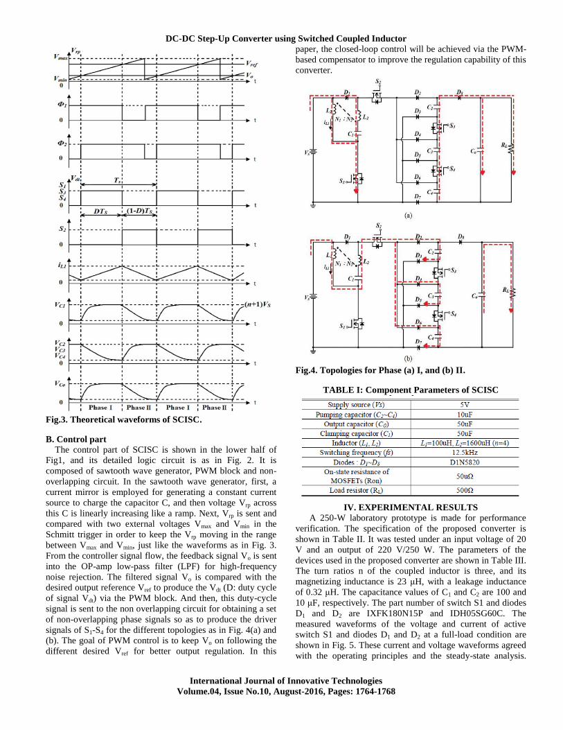
theoretical waveforms of SCISC in a switching cycle TS
(TS=1/fS, fS: switch frequency). Each TS contains two phases:
Phase I and II. The operations for Phase I and II are described
as follows.
Fig.1. Closed-loop configuration of SCISC.
Fig.2. Detailed circuit of control part.
Phase I: While Vdt =1 (PWM ON), turn on S1, S3, S4, and
turn off S2. Then, the diodes D1, D8 are turned on, and D2-D7
is off. The current-flow path is shown as “---“in Fig. 4(a). The
inductors L1, L2 and capacitor C1 are charged in parallel by
the source Vs. At the same time, C2-C4 is discharged in series
to transfer the energy to output capacitor Co and load RL.
Phase II: While Vdt =0 (PWM OFF), turn off S1, S3, S4, and
turn on S2. Then, the diodes D2-D7 are turned on, and D1, D8
are off. The current-flow path is shown as “---“in Fig. 4(b).
The capacitors C2-C4 are charged in parallel by the series
voltages of inductors L1, L2 and capacitor C1. Simultaneously,
output capacitor Co just stands alone to supply load RL.
Based on the scheduled operations of Phase I and II
cyclically, the overall step-up gain can reach the value of
3(2+n-D)/ (1-D) theoretically. Extending the capacitor count,
the gain can reach up to the value of m (2+n-D)/ (1-D) where
m is the number of pumping capacitors.
DC-DC Step-Up Converter using Switched Coupled Inductor
International Journal of Innovative Technologies
Volume.04, Issue No.10, August-2016, Pages: 1764-1768
Fig.3. Theoretical waveforms of SCISC.
B. Control part
The control part of SCISC is shown in the lower half of
Fig1, and its detailed logic circuit is as in Fig. 2. It is
composed of sawtooth wave generator, PWM block and non-
overlapping circuit. In the sawtooth wave generator, first, a
current mirror is employed for generating a constant current
source to charge the capacitor C, and then voltage Vrp across
this C is linearly increasing like a ramp. Next, Vrp is sent and
compared with two external voltages Vmax and Vmin in the
Schmitt trigger in order to keep the Vrp moving in the range
between Vmax and Vmin, just like the waveforms as in Fig. 3.
From the controller signal flow, the feedback signal Vo is sent
into the OP-amp low-pass filter (LPF) for high-frequency
noise rejection. The filtered signal Vo is compared with the
desired output reference Vref to produce the Vdt (D: duty cycle
of signal Vdt) via the PWM block. And then, this duty-cycle
signal is sent to the non overlapping circuit for obtaining a set
of non-overlapping phase signals so as to produce the driver
signals of S1-S4 for the different topologies as in Fig. 4(a) and
(b). The goal of PWM control is to keep Vo on following the
different desired Vref for better output regulation. In this
paper, the closed-loop control will be achieved via the PWM-
based compensator to improve the regulation capability of this
converter.
Fig.4. Topologies for Phase (a) I, and (b) II.
TABLE I: Component Parameters of SCISC
IV. EXPERIMENTAL RESULTS
A 250-W laboratory prototype is made for performance
verification. The specification of the proposed converter is
shown in Table II. It was tested under an input voltage of 20
V and an output of 220 V/250 W. The parameters of the
devices used in the proposed converter are shown in Table III.
The turn ratios n of the coupled inductor is three, and its
magnetizing inductance is 23 μH, with a leakage inductance
of 0.32 μH. The capacitance values of C1 and C2 are 100 and
10 μF, respectively. The part number of switch S1 and diodes
D1 and D2 are IXFK180N15P and IDH05SG60C. The
measured waveforms of the voltage and current of active
switch S1 and diodes D1 and D2 at a full-load condition are
shown in Fig. 5. These current and voltage waveforms agreed
with the operating principles and the steady-state analysis.

P. RADHA RANI, J. NAGARAJUNA BABU
International Journal of Innovative Technologies
Volume.04, Issue No.10, August-2016, Pages: 1764-1768
Fig. 6 illustrates the proposed converter efficiency curve,
which shows that the maximum efficiency is 97.2% at a light-
load (10W) operation, and the full-load efficiency is about
93.6%. Fig.6 also shows the duty cycle versus the output load.
The output load is set to be larger than 100 W to make the
proposed converter operate under the CCM operation with a
duty ratio of 60%. Under the DCM operation, the duty ratio
will be gradually decreased with the load to keep the output
voltage at 220 V. Fig. 7 shows the hardware prototype.
TABLE II: Specification of the Proposed Converter
TABLE III: Devices of the Proposed Converter
Fig.5. Current and voltage waveforms of (a) active switch
S1, (b) diode D1, and (c) output diode D2.
Fig.6. Efficiency curve of the proposed converter.
Fig.7. Hardware prototype of the proposed converter.
V. CONCLUSION
A closed-loop high-gain SCISC converter is proposed by
combining a sawtooth wave generator, PWM-based
compensator and non-overlapping circuit for step-up DC-DC
conversion and regulation. The advantages of the proposed
scheme are listed as follows. (i) In the SCISC, the large
conversion ratio can be achieved with four switches and five
capacitors for a step-up gain of 37 or above. (ii) As for the
higher step-up gain, it is easily realized through increasing the
turn ratio or extending the number of pumping capacitors. (iii)
The PWM technique is adopted here not only to enhance
output regulation capability for the different desired output,
but also to reinforce the output robustness against
source/loading/reference variation. At present, the prototype
circuit of the proposed converter is implemented in the
laboratory as some experimental results will be obtained and
measured for the verification of the proposed converter.
VI. REFERENCES
[1] Shih-Ming Chen, Member, IEEE, Man-Long Lao, Yi-
Hsun Hsieh, Tsorng-Juu Liang, Senior Member, IEEE, and
Kai-Hui Chen, “A Novel Switched-Coupled-Inductor DC–DC
Step-Up Converter and Its Derivatives”, IEEE Transactions
on Industry Applications, Vol. 51, No. 1, January/February
2015.

DC-DC Step-Up Converter using Switched Coupled Inductor
International Journal of Innovative Technologies
Volume.04, Issue No.10, August-2016, Pages: 1764-1768
[2] B. Axelrod and Y. Berkovich, “Switched-coupled inductor
cell for DC–DC converters with very large conversion ratio,”
IET Power Electron., vol. 4, no. 3, pp. 309–315, Mar. 2011.
[3] B. Axelrod, Y. Berkovich, and A. Ioinovici, “Switched-
capacitor/switched-inductor structures for getting transformer
less hybrid DC–DC PWM converters,” IEEE Trans. Circuits
Syst. I, Reg. Papers, vol. 55, no. 2, pp. 687–696, Mar. 2008.
[4] D. Li, P. C. Loh, M. Zhu, F. Gao, and F. Blaabjerg,
“Generalized multi-cell switched-inductor and switched-
capacitor Z-source inverters,” IEEE Trans. Power Electron.,
vol. 28, no. 2, pp. 837–848, Feb. 2013.
[5] L. S. Yang, T. J. Liang, and J. F. Chen, “Transformer less
DC–DC converters with high step-up voltage gain,” IEEE
Trans. Ind. Electron., vol. 56, no. 8, pp. 3144–3152, Aug.
2009.
[6] C. M. Young, M. H. Chen, T. A. Chang, C. C. Ko, and K.
Jen, “Cascade Cockcroft–Walton voltage multiplier applied to
transformer less high step-up DC–DC converter,” IEEE
Trans. Ind. Electron., vol. 60, no. 2, pp. 523–537, Feb. 2013.
[7] Y. Jiao, F. L. Luo, and B. K. Bose, “Voltage-lift split-
inductor-type boost converters,” IET Power Electron., vol. 4,
no. 4, pp. 353–362, Apr. 2011.
[8] Q. Zhao and F. C. Lee, “High-efficiency, high step-up
DC–DC converters,” IEEE Trans. Power Electron., vol. 18,
no. 1, pp. 65–73, Jan. 2003.
[9] W. Li, X. Xiang, C. Li, W. Li, and X. He, “Interleaved
high step-up ZVT converter with built-in transformer voltage
doubler cell for distributed PV generation system,” IEEE
Trans. Power Electron., vol. 28, no. 1, pp. 300–313, Jan.
2013.
[10] S.M. Chen, T. J. Liang, L. S. Yang, and J. F. Chen, “A
cascaded high step up DC–DC converter with single switch
for micro-source applications,” IEEE Trans. Power Electron.,
vol. 26, no. 4, pp. 1146–1153, Apr. 2011.
[11] S. K. Changchien, T. J. Liang, J. F. Chen, and L. S.
Yang, “Novel high step-up DC–DC converter for fuel cell
energy conversion system,” IEEE Trans. Ind. Electron., vol.
57, no. 6, pp. 2007–2017, Jun. 2010.
[12] S. Zhang, J. Xu, and P. Yang, “A single-switch high gain
quadratic boost converter based on voltage-lift-technique,” in
Proc. IPEC, 2012, pp. 71–75.