DC-DC CONVERTER FOR FUEL CELL AND HYBRID VEHICLES
65
U.S. Department of Energy FreedomCAR and Vehicle Technologies, EE-2G 1000 Independence Avenue, S.W. Washington, D.C. 20585-0121 FY 2007 DC-DC CONVERTER FOR FUEL CELL AND HYBRID VEHICLES Prepared by: Oak Ridge National Laboratory Mitch Olszewski, Program Manager Submitted to: Energy Efficiency and Renewable Energy FreedomCAR and Vehicle Technologies Vehicle Systems Team Susan A. Rogers, Technology Development Manager July 2007
Transcript of DC-DC CONVERTER FOR FUEL CELL AND HYBRID VEHICLES
U.S. Department of Energy FreedomCAR and Vehicle Technologies, EE-2G
1000 Independence Avenue, S.W. Washington, D.C. 20585-0121
FY 2007 DC-DC CONVERTER FOR FUEL CELL AND HYBRID VEHICLES Prepared by: Oak Ridge National Laboratory Mitch Olszewski, Program Manager Submitted to: Energy Efficiency and Renewable Energy FreedomCAR and Vehicle Technologies Vehicle Systems Team Susan A. Rogers, Technology Development Manager July 2007
DC-DC Converter for Fuel Cell and Hybrid Vehicles
Final Technical Report
May 8, 2007
Dr. Lizhi Zhu
Ballard Power System/Siemens VDO
15001 Commerce Drive North
Dearborn, Michigan 48120
Appendices
July 2007
Laura D. Marlino
Oak Ridge National Laboratory
Oak Ridge, Tennessee
Subcontract No: 4000029752 Final Technical Report

Table of Contents
1 PROJECT MANAGEMENT TEAM ................................................................................................................ 3 2 OBJECTIVES..................................................................................................................................................... 4 3 TECHNICAL APPROACHES .......................................................................................................................... 4 3.1 Converter Topology ................................................................................................................................... 4 3.2 Integrated Module-Based dc-dc Converter................................................................................................. 5 3.3 Planar Magnetics with Enhanced Cooling.................................................................................................. 6 4 MAJOR ACCOMPLISHMENTS OF FISCAL YEAR 2004–2007................................................................... 7 4.1 Technical Achievements Highlights in FY2004 ........................................................................................ 8 4.1.1 Topology simulation ....................................................................................................................... 8 4.1.2 Parameter design and component selection .................................................................................... 9 4.1.3 Efficiency calculation ..................................................................................................................... 9 4.1.4 Planar transformer design ............................................................................................................... 10 4.2 Technical Achievements Highlights in FY2005 ........................................................................................ 10 4.2.1 Key technologies proven out........................................................................................................... 10 4.2.2 Fully-functional, alpha unit prototype design and fabrication ........................................................ 13 4.2.3 High volume cost estimation .......................................................................................................... 15 4.2.4 Alpha prototype test results............................................................................................................. 16 4.2.5 Technical discussion ....................................................................................................................... 17 4.2.6 Conclusion for FY2005................................................................................................................... 18 4.3 Technical Achievements Highlights in FY2006 ........................................................................................ 19 4.3.1 Continued electrical evaluation test on alpha prototype ................................................................. 19 4.3.2 Cost reduction – Beta design .......................................................................................................... 20 4.3.3 Volume and weight reduction ......................................................................................................... 20 4.3.4 Thermal design improvement ......................................................................................................... 23 4.3.5 Coolant channel final design........................................................................................................... 24 4.3.6 Solving practical issue .................................................................................................................... 26 4.3.7 Conclusion for FY2006................................................................................................................... 27 4.4 Technical Achievements Highlights in FY2007 ........................................................................................ 28 4.4.1 Manufacturing process development – power module process ...................................................... 28 4.4.2 Manufacturing process development – pilot plant process ............................................................. 29 4.4.3 Beta prototype fabrication .............................................................................................................. 31 4.4.4 Beta dc-dc converter prototype final testing .................................................................................. 31 5 FINAL PROGRAM REVIEW AND WITNESS TEST..................................................................................... 34 5.1 Beta Prototype Size and Dimensions ......................................................................................................... 34 5.2 Beta Prototype Weight .............................................................................................................................. 36 5.3 Final Program Review and Witness Test ................................................................................................... 38 5.3.1 Final test result summary and DOE goal achieved ........................................................................ 38 5.3.2 Witness test ..................................................................................................................................... 39 6 EXECUTIVE SUMMARY AND FUTURE DIRECTIONS ............................................................................ 41 6.1 Summary .................................................................................................................................................... 41 6.2 Future Directions........................................................................................................................................ 42 6.2.1 Weight reduction ............................................................................................................................ 42 6.2.2 Cost reduction ................................................................................................................................. 43 7 PUBLICATIONS .............................................................................................................................................. 44 APPENDIX: ORNL TEST VERIFICATION......................................................................................................... 45
Subcontract No: 4000029752 Final Technical Report

Page 3 of 64
Subcontract No: 4000029752 Final Technical Report
PROJECT MANAGEMENT TEAM
Principal Investigator: Dr. Lizhi Zhu Ballard Power Systems (Siemens VDO Automotive Corporation) 15001 Commerce Drive North Dearborn, MI 48120 Voice: 313-354-5973; Fax: 313-583-5990; E-mail: [email protected] Project Manager: David Blanck Ballard Power Systems (Siemens VDO Automotive Corporation) 15001 Commerce Drive North Dearborn, MI 48120 Voice: 313-434-1947; Fax: 313-583-5990; E-mail: [email protected] ORNL Program Manager: Laura Marlino Voice: (865) 946-1245; Fax: 865-946-1262; E-mail: [email protected] DOE Technology Development Manager: Susan A. Rogers Voice: 202-586-8997; Fax: 202-586-1600; E-mail: [email protected]
Page 4 of 64
Subcontract No: 4000029752 Final Technical Report
2 OBJECTIVES The goal of this project is to develop and fabricate a 5kW dc-dc converter with a baseline 14V output
capability for fuel cell and hybrid vehicles. The major objectives for this dc-dc converter technology
are to meet:
• Higher efficiency (92%)
• High coolant temperature,e capability (105°C) ,
• High reliability (15 Years/150,000miles),
• Smaller volume (5L),
• Lower weight (6kg), and
• Lower cost ($75/kW).
3 TECHNICAL APPROACHES The key technical challenge for these converters is the 105°C coolant temperatures. The power
switches and magnetics must be designed to sustain these operating temperatures reliably, without
a large cost/mass/volume penalty. The following key technologies are proposed to break through
technical barriers to achieve high temperature, high power density, and lower cost design.
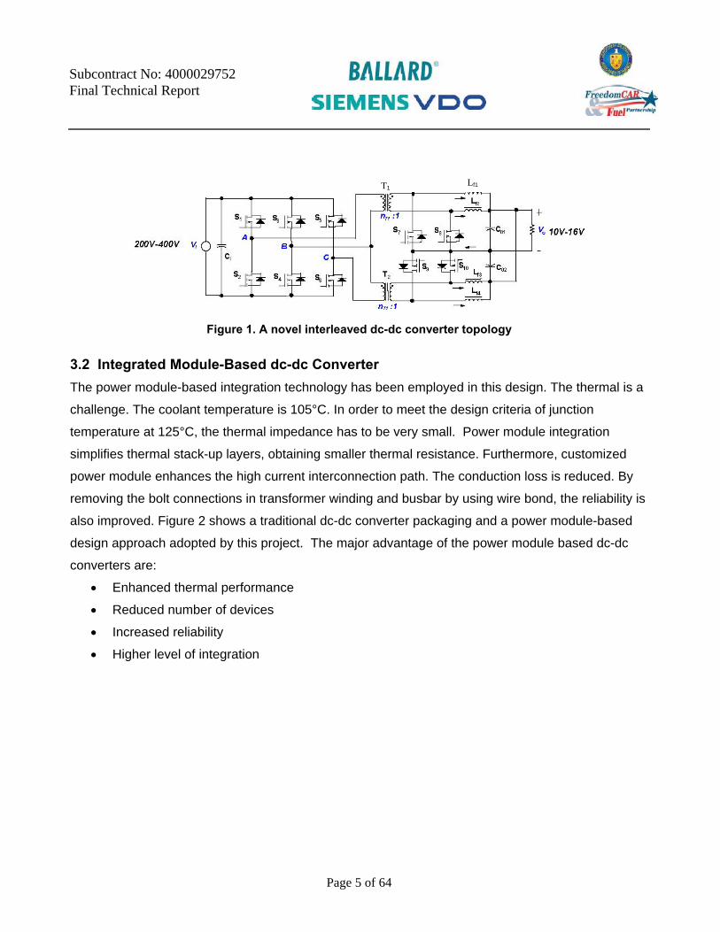
3.1 Converter Topology A novel interleaved dc-dc converter topology is proposed for this high power conversion, as
shown in Figure 1. The key merits of the converter are:
• Lower RMS current stresses on components due to interleaving,
• Reduced ripple current on capacitors due to interleaving,
• Lower power losses due to low Rds_on and soft-switching,
• Smaller magnetics due to high switching frequency, and
• Low EMI due to integrated power devices and magnetics.
Page 5 of 64
Subcontract No: 4000029752 Final Technical Report
Figure 1. A novel interleaved dc-dc converter topology
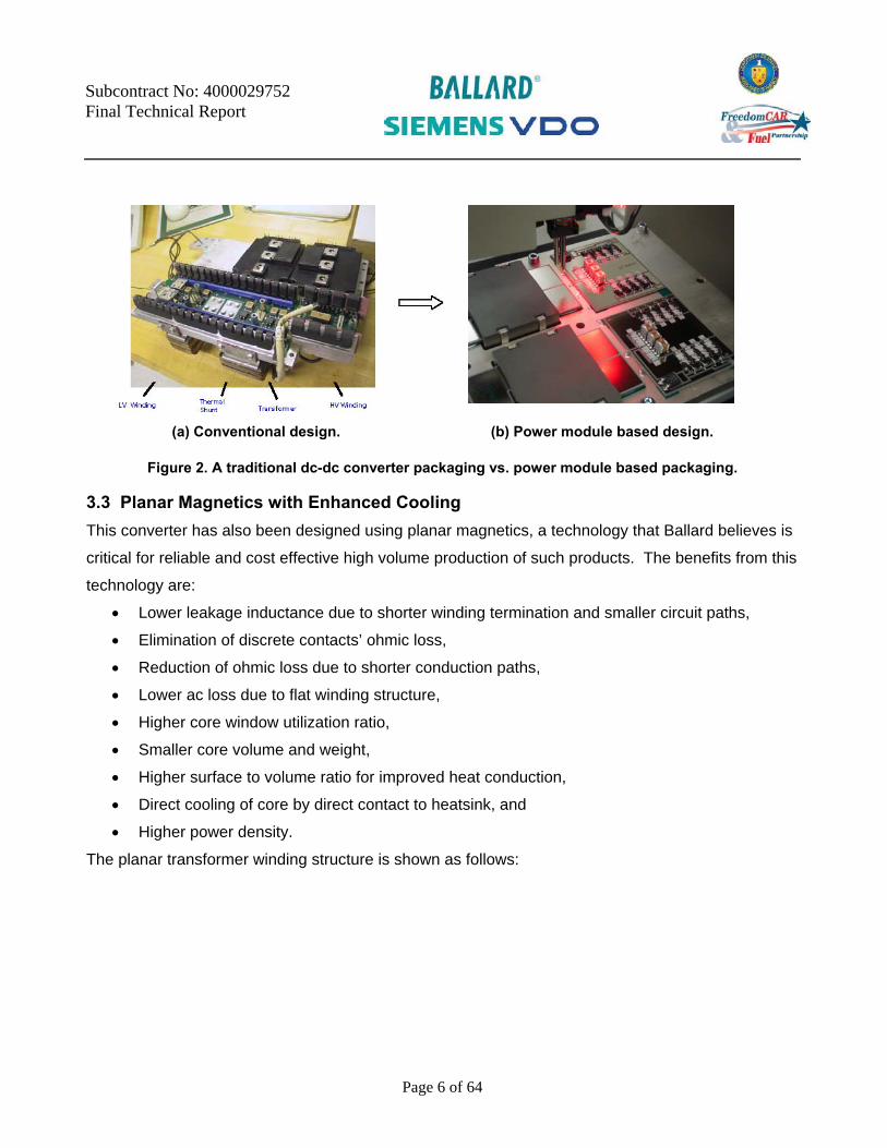
3.2 Integrated Module-Based dc-dc Converter The power module-based integration technology has been employed in this design. The thermal is a
challenge. The coolant temperature is 105°C. In order to meet the design criteria of junction
temperature at 125°C, the thermal impedance has to be very small. Power module integration
simplifies thermal stack-up layers, obtaining smaller thermal resistance. Furthermore, customized
power module enhances the high current interconnection path. The conduction loss is reduced. By
removing the bolt connections in transformer winding and busbar by using wire bond, the reliability is
also improved. Figure 2 shows a traditional dc-dc converter packaging and a power module-based
design approach adopted by this project. The major advantage of the power module based dc-dc
converters are:
• Enhanced thermal performance
• Reduced number of devices
• Increased reliability
• Higher level of integration
Lf1 T1
Page 6 of 64
Subcontract No: 4000029752 Final Technical Report
(a) Conventional design. (b) Power module based design.
Figure 2. A traditional dc-dc converter packaging vs. power module based packaging.
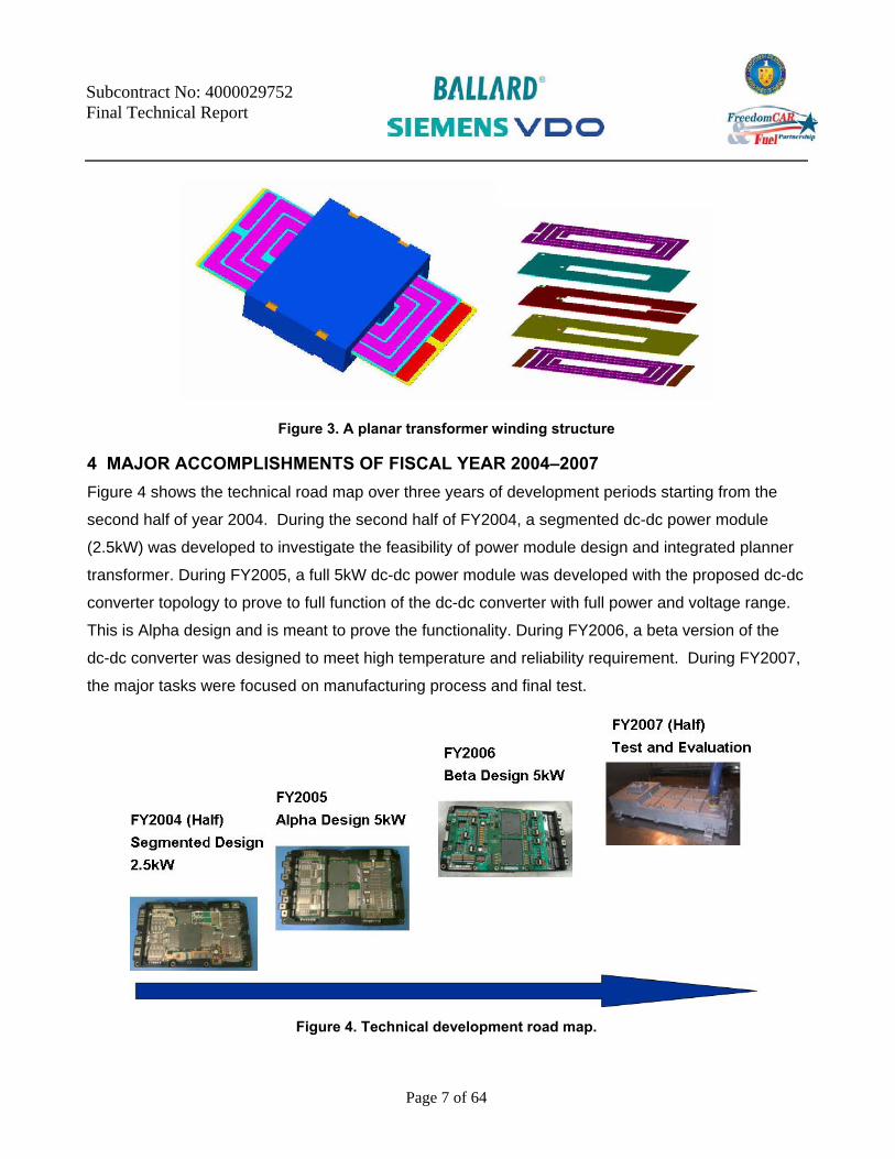
3.3 Planar Magnetics with Enhanced Cooling This converter has also been designed using planar magnetics, a technology that Ballard believes is
critical for reliable and cost effective high volume production of such products. The benefits from this
technology are:
• Lower leakage inductance due to shorter winding termination and smaller circuit paths,
• Elimination of discrete contacts’ ohmic loss,
• Reduction of ohmic loss due to shorter conduction paths,
• Lower ac loss due to flat winding structure,
• Higher core window utilization ratio,
• Smaller core volume and weight,
• Higher surface to volume ratio for improved heat conduction,
• Direct cooling of core by direct contact to heatsink, and
• Higher power density.
The planar transformer winding structure is shown as follows:
Page 7 of 64
Subcontract No: 4000029752 Final Technical Report
Figure 3. A planar transformer winding structure
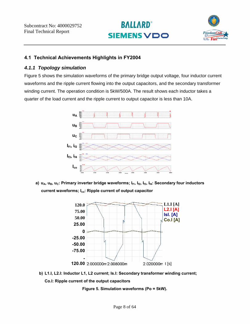
4 MAJOR ACCOMPLISHMENTS OF FISCAL YEAR 2004–2007 Figure 4 shows the technical road map over three years of development periods starting from the
second half of year 2004. During the second half of FY2004, a segmented dc-dc power module
(2.5kW) was developed to investigate the feasibility of power module design and integrated planner
transformer. During FY2005, a full 5kW dc-dc power module was developed with the proposed dc-dc
converter topology to prove to full function of the dc-dc converter with full power and voltage range.
This is Alpha design and is meant to prove the functionality. During FY2006, a beta version of the
dc-dc converter was designed to meet high temperature and reliability requirement. During FY2007,
the major tasks were focused on manufacturing process and final test.
Figure 4. Technical development road map.
Page 8 of 64
Subcontract No: 4000029752 Final Technical Report
4.1 Technical Achievements Highlights in FY2004
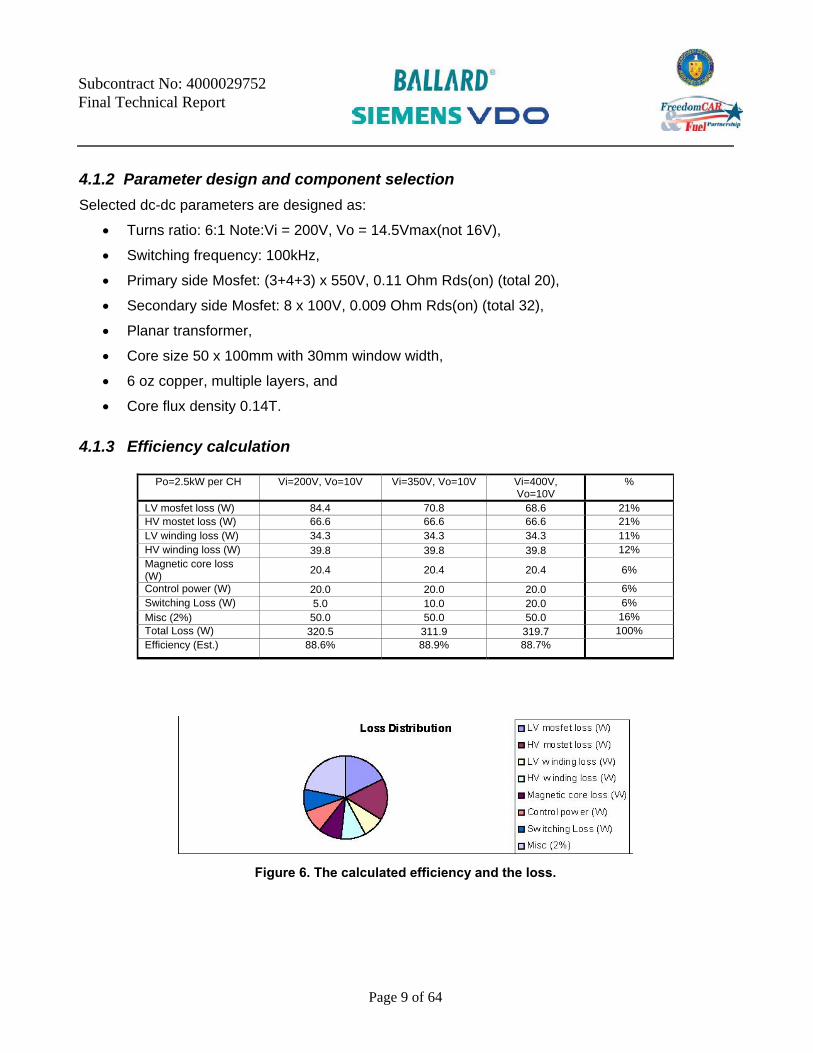
4.1.1 Topology simulation Figure 5 shows the simulation waveforms of the primary bridge output voltage, four inductor current
waveforms and the ripple current flowing into the output capacitors, and the secondary transformer
winding current. The operation condition is 5kW/500A. The result shows each inductor takes a
quarter of the load current and the ripple current to output capacitor is less than 10A.
a) uA, uB, uC: Primary inverter bridge waveforms; If1, If2, If3, If4: Secondary four inductors
current waveforms; Ico: Ripple current of output capacitor
b) L1.I, L2.I: Inductor L1, L2 current; Is.I: Secondary transformer winding current;
Co.I: Ripple current of the output capacitors
Figure 5. Simulation waveforms (Po = 5kW).
uA
uB
uC
If1, if2
If3, if4
Ico
120.0 75.00 50.00 25.00
0 -25.00 -50.00 -75.00
-120.00
L1.I [A] L2.I [A] IsI. [A] Co.I [A]
t [s]
Page 9 of 64
Subcontract No: 4000029752 Final Technical Report
4.1.2 Parameter design and component selection Selected dc-dc parameters are designed as:
• Turns ratio: 6:1 Note:Vi = 200V, Vo = 14.5Vmax(not 16V),
• Switching frequency: 100kHz,
• Primary side Mosfet: (3+4+3) x 550V, 0.11 Ohm Rds(on) (total 20),
• Secondary side Mosfet: 8 x 100V, 0.009 Ohm Rds(on) (total 32),
• Planar transformer,
• Core size 50 x 100mm with 30mm window width,
• 6 oz copper, multiple layers, and
• Core flux density 0.14T.
4.1.3 Efficiency calculation
Po=2.5kW per CH Vi=200V, Vo=10V Vi=350V, Vo=10V Vi=400V, Vo=10V
%
LV mosfet loss (W) 84.4 70.8 68.6 21% HV mostet loss (W) 66.6 66.6 66.6 21% LV winding loss (W) 34.3 34.3 34.3 11% HV winding loss (W) 39.8 39.8 39.8 12% Magnetic core loss (W) 20.4 20.4 20.4 6%
Control power (W) 20.0 20.0 20.0 6% Switching Loss (W) 5.0 10.0 20.0 6% Misc (2%) 50.0 50.0 50.0 16% Total Loss (W) 320.5 311.9 319.7 100% Efficiency (Est.) 88.6% 88.9% 88.7%
Figure 6. The calculated efficiency and the loss.
Page 10 of 64
Subcontract No: 4000029752 Final Technical Report
4.1.4 Planar transformer design Planar transformer parameter:
• Turns ratio: 6:1,
• Core size 50x100mm with 30mm window width,
• 6 oz copper, multiple layers, and
• Core flux density 0.14T.
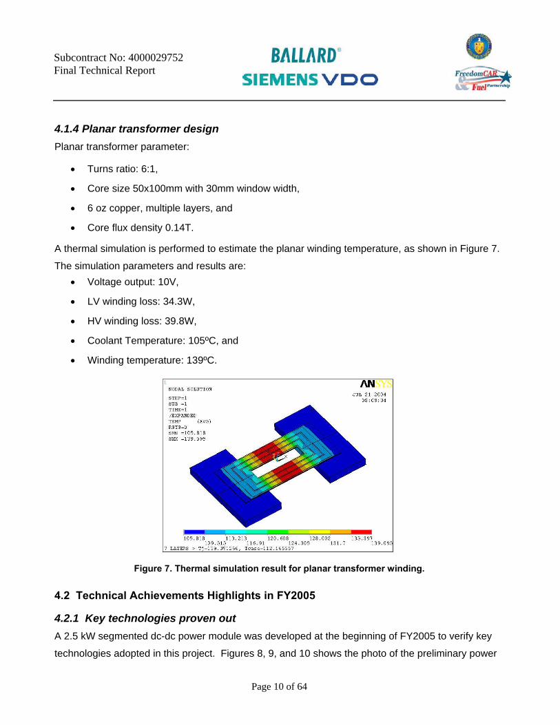
A thermal simulation is performed to estimate the planar winding temperature, as shown in Figure 7.
The simulation parameters and results are: • Voltage output: 10V,
• LV winding loss: 34.3W,
• HV winding loss: 39.8W,
• Coolant Temperature: 105ºC, and
• Winding temperature: 139ºC.
Figure 7. Thermal simulation result for planar transformer winding.
4.2 Technical Achievements Highlights in FY2005
4.2.1 Key technologies proven out A 2.5 kW segmented dc-dc power module was developed at the beginning of FY2005 to verify key
technologies adopted in this project. Figures 8, 9, and 10 shows the photo of the preliminary power
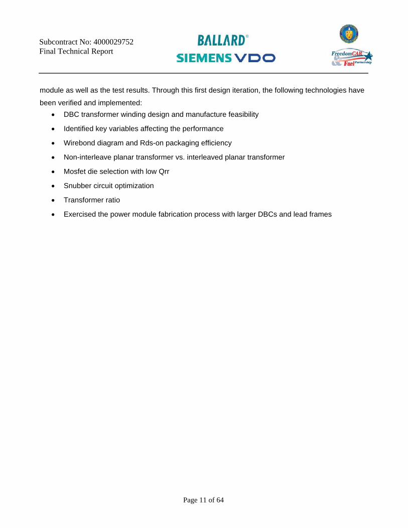
Page 11 of 64
Subcontract No: 4000029752 Final Technical Report
module as well as the test results. Through this first design iteration, the following technologies have
been verified and implemented: • DBC transformer winding design and manufacture feasibility
• Identified key variables affecting the performance
• Wirebond diagram and Rds-on packaging efficiency
• Non-interleave planar transformer vs. interleaved planar transformer
• Mosfet die selection with low Qrr
• Snubber circuit optimization
• Transformer ratio
• Exercised the power module fabrication process with larger DBCs and lead frames
Subcontract No: 4000029752 Final Technical Report
Page 11 of 43
S5_S_WB
S6_S_WB
S5_D_WB
S6_D_WB
S5_DS
S6_DS
WS_WBWS
S1_DS
S2_DS
S3_DS
S4_DS
S5_S_WB
S6_S_WB
S5_D_WB
S6_D_WB
S5_DS
S6_DS
WS_WBWS
S1_DS
S2_DS
S3_DS
S4_DS
Figure 8. A segmented preliminary 2.5kW DC-DC power module
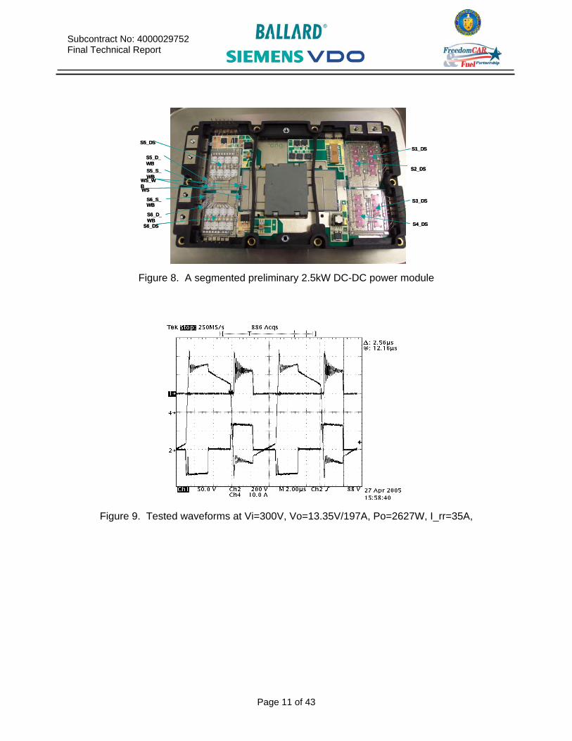
Figure 9. Tested waveforms at Vi=300V, Vo=13.35V/197A, Po=2627W, I_rr=35A,
Page 13 of 64
Subcontract No: 4000029752 Final Technical Report
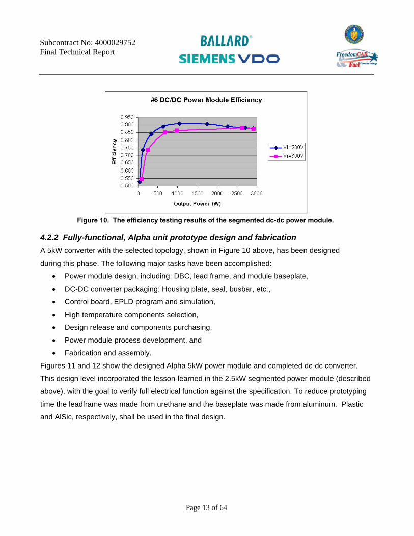
4.2.2 Fully-functional, Alpha unit prototype design and fabrication A 5kW converter with the selected topology, shown in Figure 10 above, has been designed
during this phase. The following major tasks have been accomplished:
• Power module design, including: DBC, lead frame, and module baseplate,
• DC-DC converter packaging: Housing plate, seal, busbar, etc.,
• Control board, EPLD program and simulation,
• High temperature components selection,
• Design release and components purchasing,
• Power module process development, and
• Fabrication and assembly.
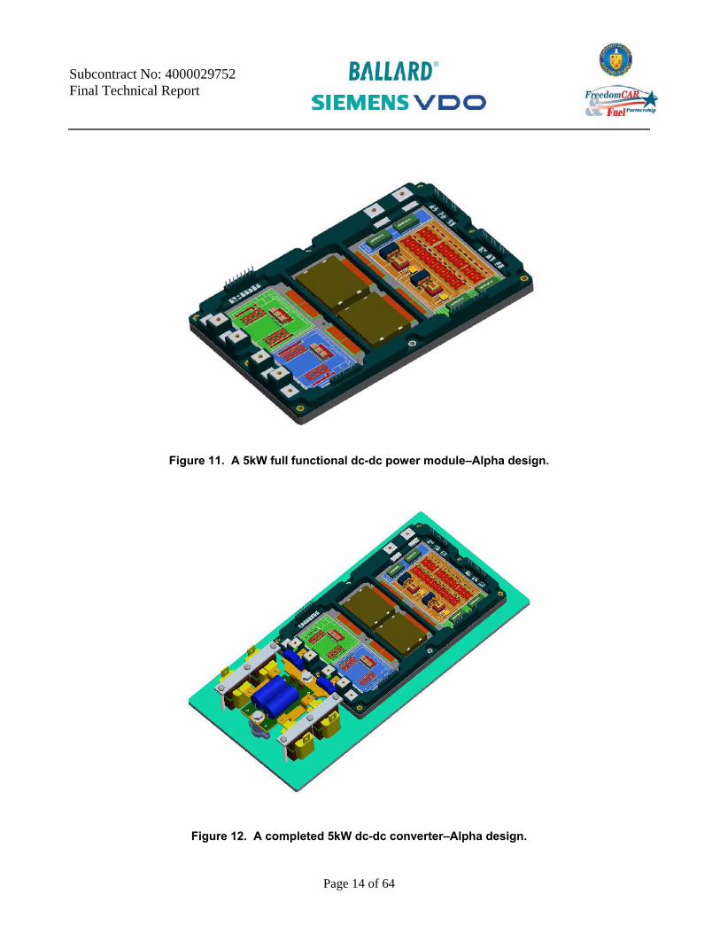
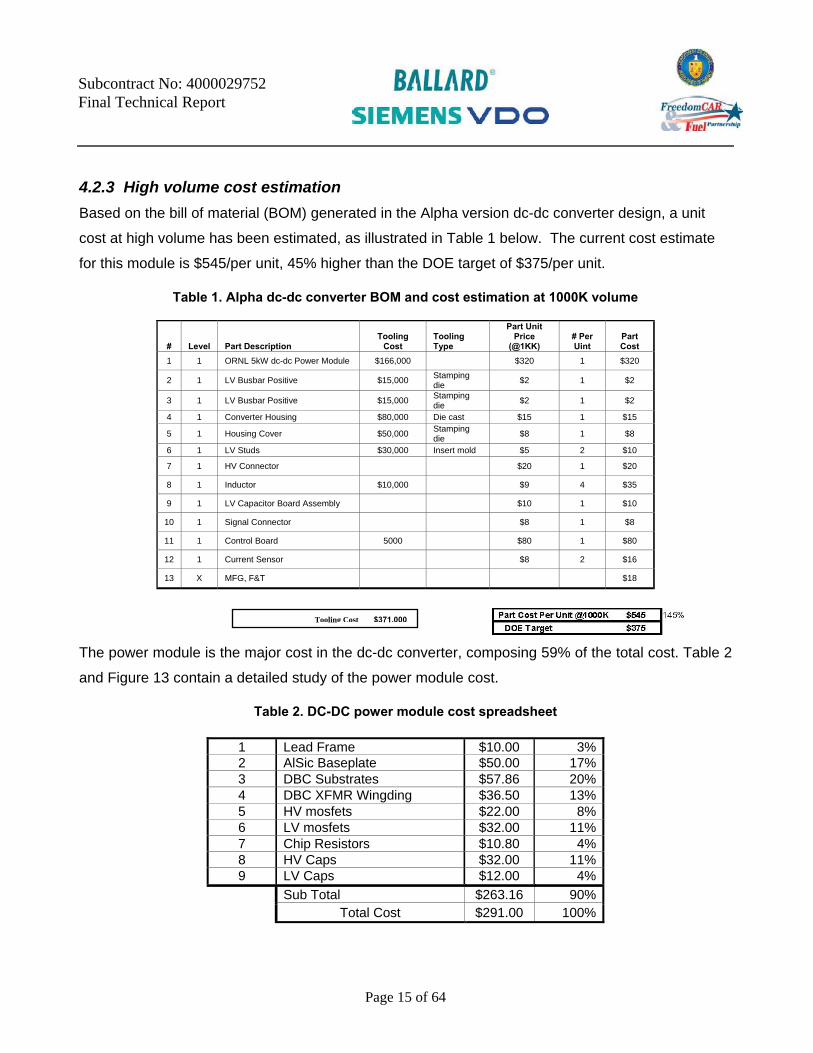
Figures 11 and 12 show the designed Alpha 5kW power module and completed dc-dc converter.
This design level incorporated the lesson-learned in the 2.5kW segmented power module (described
above), with the goal to verify full electrical function against the specification. To reduce prototyping
time the leadframe was made from urethane and the baseplate was made from aluminum. Plastic
and AlSic, respectively, shall be used in the final design.
Figure 10. The efficiency testing results of the segmented dc-dc power module.
Page 14 of 64
Subcontract No: 4000029752 Final Technical Report
Figure 11. A 5kW full functional dc-dc power module–Alpha design.
Figure 12. A completed 5kW dc-dc converter–Alpha design.
Page 15 of 64
Subcontract No: 4000029752 Final Technical Report
4.2.3 High volume cost estimation Based on the bill of material (BOM) generated in the Alpha version dc-dc converter design, a unit
cost at high volume has been estimated, as illustrated in Table 1 below. The current cost estimate
for this module is $545/per unit, 45% higher than the DOE target of $375/per unit.
Table 1. Alpha dc-dc converter BOM and cost estimation at 1000K volume
# Level Part Description Tooling
Cost Tooling Type
Part Unit Price
(@1KK) # Per Uint
Part Cost
1 1 ORNL 5kW dc-dc Power Module $166,000 $320 1 $320
2 1 LV Busbar Positive $15,000 Stamping die $2 1 $2
3 1 LV Busbar Positive $15,000 Stamping die $2 1 $2
4 1 Converter Housing $80,000 Die cast $15 1 $15
5 1 Housing Cover $50,000 Stamping die $8 1 $8
6 1 LV Studs $30,000 Insert mold $5 2 $10
7 1 HV Connector $20 1 $20
8 1 Inductor $10,000 $9 4 $35
9 1 LV Capacitor Board Assembly $10 1 $10
10 1 Signal Connector $8 1 $8
11 1 Control Board 5000 $80 1 $80
12 1 Current Sensor $8 2 $16
13 X MFG, F&T $18
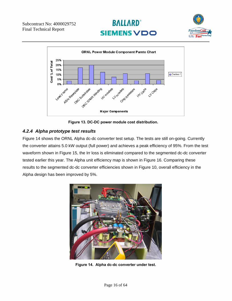
The power module is the major cost in the dc-dc converter, composing 59% of the total cost. Table 2
and Figure 13 contain a detailed study of the power module cost.
Table 2. DC-DC power module cost spreadsheet
1 Lead Frame $10.00 3% 2 AlSic Baseplate $50.00 17% 3 DBC Substrates $57.86 20% 4 DBC XFMR Wingding $36.50 13% 5 HV mosfets $22.00 8% 6 LV mosfets $32.00 11% 7 Chip Resistors $10.80 4% 8 HV Caps $32.00 11% 9 LV Caps $12.00 4%
Sub Total $263.16 90% Total Cost $291.00 100%
Tooling Cost $371,000
Page 16 of 64
Subcontract No: 4000029752 Final Technical Report
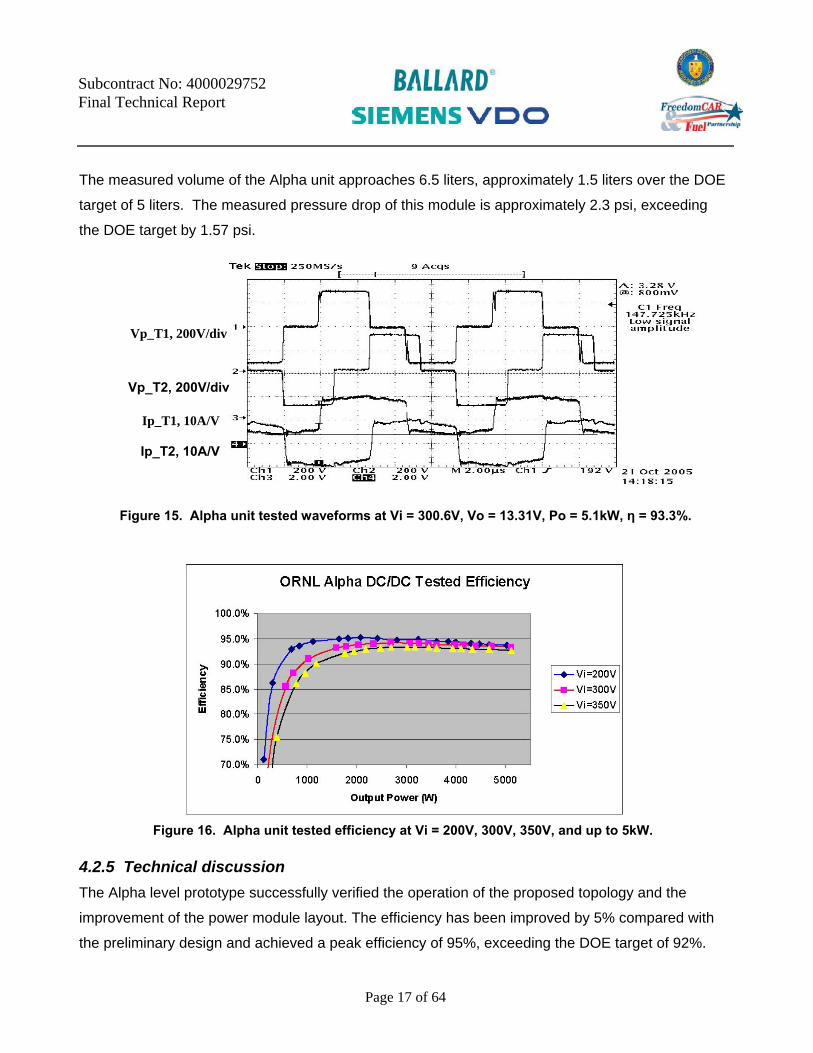
4.2.4 Alpha prototype test results Figure 14 shows the ORNL Alpha dc-dc converter test setup. The tests are still on-going. Currently
the converter attains 5.0 kW output (full power) and achieves a peak efficiency of 95%. From the test
waveform shown in Figure 15, the Irr loss is eliminated compared to the segmented dc-dc converter
tested earlier this year. The Alpha unit efficiency map is shown in Figure 16. Comparing these
results to the segmented dc-dc converter efficiencies shown in Figure 10, overall efficiency in the
Alpha design has been improved by 5%.
Figure 14. Alpha dc-dc converter under test.
Figure 13. DC-DC power module cost distribution.
Page 17 of 64
Subcontract No: 4000029752 Final Technical Report
The measured volume of the Alpha unit approaches 6.5 liters, approximately 1.5 liters over the DOE
target of 5 liters. The measured pressure drop of this module is approximately 2.3 psi, exceeding
the DOE target by 1.57 psi.
Figure 15. Alpha unit tested waveforms at Vi = 300.6V, Vo = 13.31V, Po = 5.1kW, η = 93.3%.
4.2.5 Technical discussion The Alpha level prototype successfully verified the operation of the proposed topology and the
improvement of the power module layout. The efficiency has been improved by 5% compared with
the preliminary design and achieved a peak efficiency of 95%, exceeding the DOE target of 92%.
Vp_T1, 200V/div
Vp_T2, 200V/div
Figure 16. Alpha unit tested efficiency at Vi = 200V, 300V, 350V, and up to 5kW.
Ip_T1, 10A/V
Ip_T2, 10A/V
Page 18 of 64
Subcontract No: 4000029752 Final Technical Report
However, we have found several issues that must be improved in the final Beta level design. These
issues include:
• High volume cost target,
• Power density improvement towards the DOE target,
• Large DBC size (87mmX112mm) exceeds the supplier’s zone of comfort and has reliability,
implications (thermally cycling),
• Large lead frame results in excessive tooling costs,
• Large module baseplate approaches limit of production facility capabilities, and
• Higher pressure drop than target.
4.2.6 Conclusion for FY2005 • The key technologies have been proven out in Phase I,
• Alpha converter prototype has been designed in Phase II,
• All components have been received and the system has been assembled,
• High volume cost estimates have been developed,
• Achieved full power output (5kW),
• Efficiency has been improved by 5% compared to preliminary design,
• Volume and pressure drop of the Alpha design has been tested, and
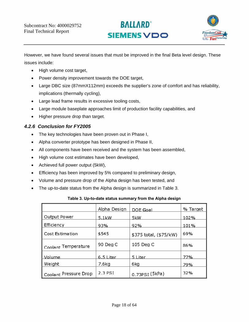
• The up-to-date status from the Alpha design is summarized in Table 3.
Table 3. Up-to-date status summary from the Alpha design
Page 19 of 64
Subcontract No: 4000029752 Final Technical Report
4.3 Technical Achievements Highlights in FY2006 In FY2006, we continued working on the Alpha prototype testing work, completed the Beta design
and part purchasing, and developed the manufacturing process to produce the final prototype.
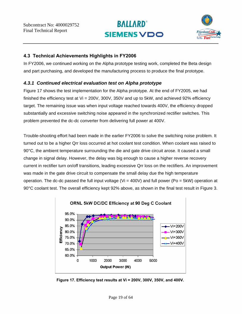
4.3.1 Continued electrical evaluation test on Alpha prototype Figure 17 shows the test implementation for the Alpha prototype. At the end of FY2005, we had
finished the efficiency test at Vi = 200V, 300V, 350V and up to 5kW, and achieved 92% efficiency
target. The remaining issue was when input voltage reached towards 400V, the efficiency dropped
substantially and excessive switching noise appeared in the synchronized rectifier switches. This
problem prevented the dc-dc converter from delivering full power at 400V.
Trouble-shooting effort had been made in the earlier FY2006 to solve the switching noise problem. It
turned out to be a higher Qrr loss occurred at hot coolant test condition. When coolant was raised to
90°C, the ambient temperature surrounding the die and gate drive circuit arose. It caused a small
change in signal delay. However, the delay was big enough to cause a higher reverse recovery
current in rectifier turn on/off transitions, leading excessive Qrr loss on the rectifiers. An improvement
was made in the gate drive circuit to compensate the small delay due the high temperature
operation. The dc-dc passed the full input voltage (Vi = 400V) and full power (Po = 5kW) operation at
90°C coolant test. The overall efficiency kept 92% above, as shown in the final test result in Figure 3.
Figure 17. Efficiency test results at Vi = 200V, 300V, 350V, and 400V.
Page 20 of 64
Subcontract No: 4000029752 Final Technical Report
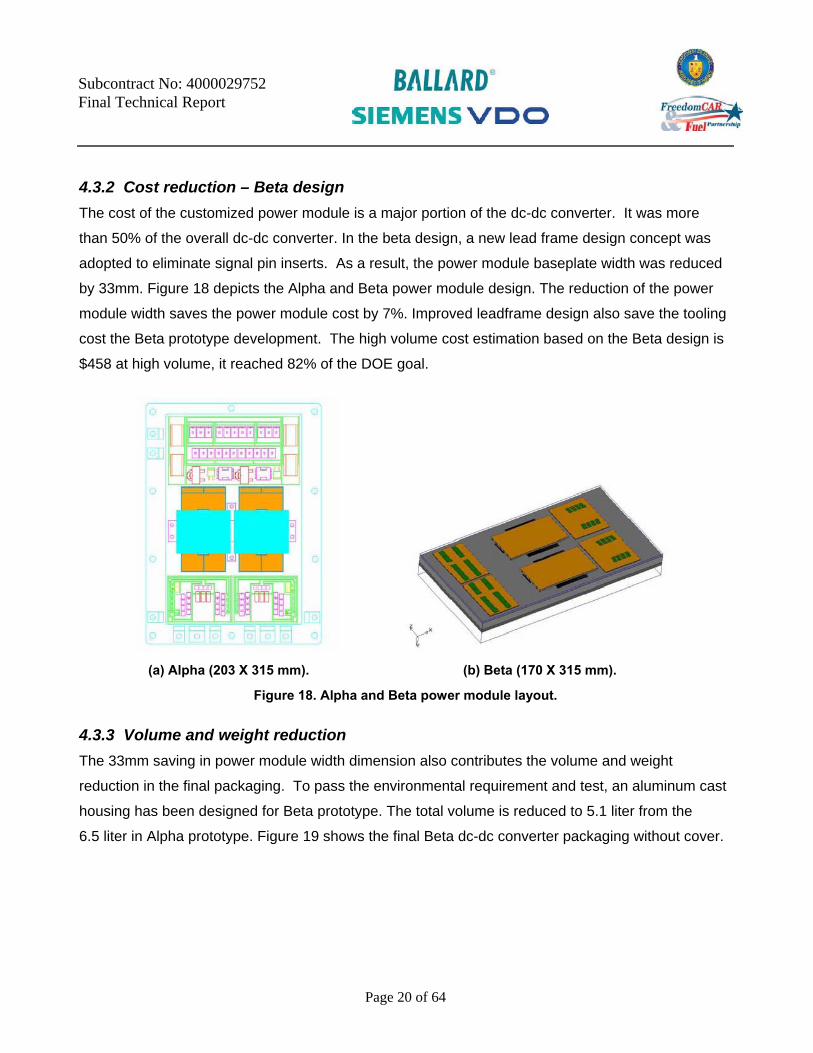
4.3.2 Cost reduction – Beta design The cost of the customized power module is a major portion of the dc-dc converter. It was more
than 50% of the overall dc-dc converter. In the beta design, a new lead frame design concept was
adopted to eliminate signal pin inserts. As a result, the power module baseplate width was reduced
by 33mm. Figure 18 depicts the Alpha and Beta power module design. The reduction of the power
module width saves the power module cost by 7%. Improved leadframe design also save the tooling
cost the Beta prototype development. The high volume cost estimation based on the Beta design is
$458 at high volume, it reached 82% of the DOE goal.
(a) Alpha (203 X 315 mm). (b) Beta (170 X 315 mm).
Figure 18. Alpha and Beta power module layout.
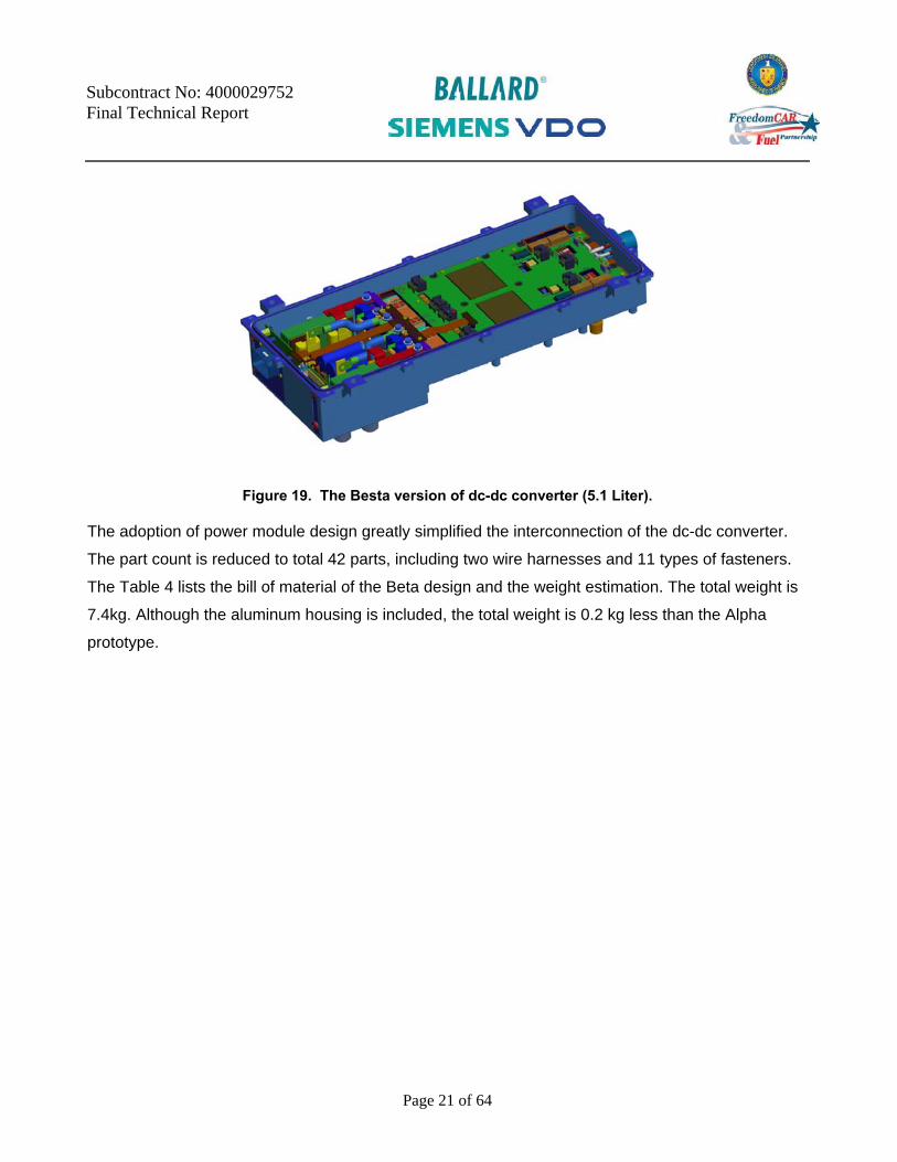
4.3.3 Volume and weight reduction The 33mm saving in power module width dimension also contributes the volume and weight
reduction in the final packaging. To pass the environmental requirement and test, an aluminum cast
housing has been designed for Beta prototype. The total volume is reduced to 5.1 liter from the
6.5 liter in Alpha prototype. Figure 19 shows the final Beta dc-dc converter packaging without cover.
Page 21 of 64
Subcontract No: 4000029752 Final Technical Report
Figure 19. The Besta version of dc-dc converter (5.1 Liter).
The adoption of power module design greatly simplified the interconnection of the dc-dc converter.
The part count is reduced to total 42 parts, including two wire harnesses and 11 types of fasteners.
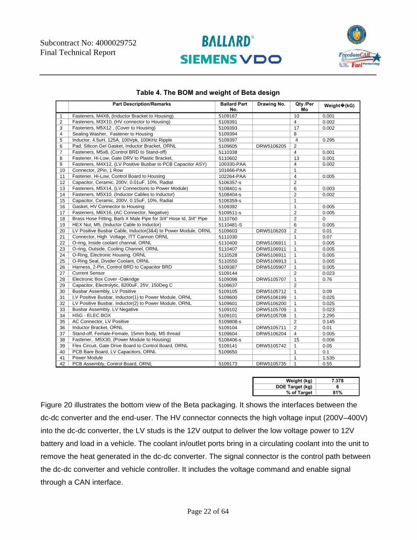
The Table 4 lists the bill of material of the Beta design and the weight estimation. The total weight is
7.4kg. Although the aluminum housing is included, the total weight is 0.2 kg less than the Alpha
prototype.
Page 22 of 64
Subcontract No: 4000029752 Final Technical Report
Table 4. The BOM and weight of Beta design Part Description/Remarks Ballard Part
No. Drawing No. Qty /Per
Mo Weight�(kG)
1 Fasteners, M4X8, (Inductor Bracket to Housing) 5109167 10 0.001 2 Fasteners, M3X10, (HV connector to Housing) 5109391 4 0.002 3 Fasteners, M5X12 , (Cover to Housing) 5109393 17 0.002 4 Sealing Washer, Fastener to Housing 5109394 8 5 Inductor, 4.5uH, 125A, 100Vpk, 100KHz Ripple 5109397 4 0.295 6 Pad, Silicon Gel Gasket, Inductor Bracket, ORNL 5109605 DRW5106205 2 7 Fasteners, M5x8, (Control BRD to Stand-off) 5110338 4 0.001 8 Fastener, Hi-Low, Gate DRV to Plastic Bracket, 5110602 13 0.001 9 Fasteners, M4X12, (LV Positive Busbar to PCB Capacitor ASY) 100330-PAA 4 0.002 10 Connector, 2Pin, 1 Row 101666-PAA 1 11 Fastener, Hi-Low, Control Board to Housing 102264-PAA 4 0.005 12 Capacitor, Ceramic, 200V, 0.01uF, 10%, Radial 5106357-s 2 13 Fasteners, M5X14, (LV Connections to Power Module) 5108401-s 6 0.003 14 Fasteners, M5X10, (Inductor Cables to Inductor) 5108404-s 2 0.002 15 Capacitor, Ceramic, 200V, 0.15uF, 10%, Radial 5106359-s 1 16 Gasket, HV Connector to Housing 5109392 1 0.005 17 Fasteners, M6X16, (AC Connector, Negative) 5109511-s 2 0.005 18 Brass Hose Fitting, Barb X Male Pipe for 3/4" Hose Id, 3/4" Pipe 5110760 2 0 19 HEX Nut, M5, (Inductor Cable to Inductor) 5110481-S 6 0.005 20 LV Positive Busbar Cable, Inductor(3&4) to Power Module, ORNL 5109603 DRW5106203 2 0.01 21 Connector, High Voltage, ITT Cannon ORNL 5111030 1 0.07 22 O-ring, Inside coolant channal, ORNL 5110400 DRW5106911 1 0.005 23 O-ring, Outside, Cooling Channel, ORNL 5110407 DRW5106911 1 0.005 24 O-Ring, Electronic Housing, ORNL 5110528 DRW5106911 1 0.005 25 O-Ring Seal, Divider Coolant, ORNL 5110550 DRW5106913 1 0.005 26 Harness, 2-Pin, Control BRD to Capacitor BRD 5109387 DRW5105907 1 0.005 27 Current Sensor 5109144 2 0.023 28 Electronic Box Cover -Oakridge 5109098 DRW5105707 1 0.76 29 Capacitor, Electrolytic, 8200uF, 25V, 150Deg C 5109637 2 30 Busbar Assembly, LV Positive 5109105 DRW5105712 1 0.09 31 LV Positive Busbar, Inductor(1) to Power Module, ORNL 5109600 DRW5106199 1 0.025 32 LV Positive Busbar, Inductor(2) to Power Module, ORNL 5109601 DRW5106200 1 0.025 33 Busbar Assembly, LV Negative 5109102 DRW5105709 1 0.023 34 HSG - ELEC BOX 5109101 DRW5105708 1 2.295 35 AC Connector, LV Positive 5109808-s 2 0.145 36 Inductor Bracket, ORNL 5109104 DRW5105711 2 0.01 37 Stand-off, Female-Female, 15mm Body, M5 thread 5109604 DRW5106204 4 0.005 38 Fastener, M5X30, (Power Module to Housing) 5108406-s 15 0.006 39 Flex Circuit, Gate Drive Board to Control Board, ORNL 5109141 DRW5105742 1 0.05 40 PCB Bare Board, LV Capacitors, ORNL 5109650 1 0.1 41 Power Module 1 1.535 42 PCB Assembly, Control Board, ORNL 5109173 DRW5105735 1 0.55
Weight (kg) 7.378
DOE Target (kg) 6 % of Target 81%
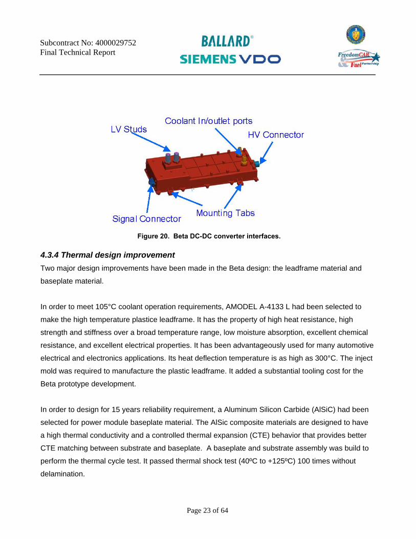
Figure 20 illustrates the bottom view of the Beta packaging. It shows the interfaces between the
dc-dc converter and the end-user. The HV connector connects the high voltage input (200V–400V)
into the dc-dc converter, the LV studs is the 12V output to deliver the low voltage power to 12V
battery and load in a vehicle. The coolant in/outlet ports bring in a circulating coolant into the unit to
remove the heat generated in the dc-dc converter. The signal connector is the control path between
the dc-dc converter and vehicle controller. It includes the voltage command and enable signal
through a CAN interface.
Page 23 of 64
Subcontract No: 4000029752 Final Technical Report
4.3.4 Thermal design improvement Two major design improvements have been made in the Beta design: the leadframe material and
baseplate material.
In order to meet 105°C coolant operation requirements, AMODEL A-4133 L had been selected to
make the high temperature plastice leadframe. It has the property of high heat resistance, high
strength and stiffness over a broad temperature range, low moisture absorption, excellent chemical
resistance, and excellent electrical properties. It has been advantageously used for many automotive
electrical and electronics applications. Its heat deflection temperature is as high as 300°C. The inject
mold was required to manufacture the plastic leadframe. It added a substantial tooling cost for the
Beta prototype development.
In order to design for 15 years reliability requirement, a Aluminum Silicon Carbide (AlSiC) had been
selected for power module baseplate material. The AlSic composite materials are designed to have
a high thermal conductivity and a controlled thermal expansion (CTE) behavior that provides better
CTE matching between substrate and baseplate. A baseplate and substrate assembly was build to
perform the thermal cycle test. It passed thermal shock test (40ºC to +125ºC) 100 times without
delamination.
Figure 20. Beta DC-DC converter interfaces.
Page 24 of 64
Subcontract No: 4000029752 Final Technical Report
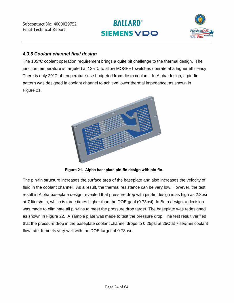
4.3.5 Coolant channel final design The 105°C coolant operation requirement brings a quite bit challenge to the thermal design. The
junction temperature is targeted at 125°C to allow MOSFET switches operate at a higher efficiency.
There is only 20°C of temperature rise budgeted from die to coolant. In Alpha design, a pin-fin
pattern was designed in coolant channel to achieve lower thermal impedance, as shown in
Figure 21.
The pin-fin structure increases the surface area of the baseplate and also increases the velocity of
fluid in the coolant channel. As a result, the thermal resistance can be very low. However, the test
result in Alpha baseplate design revealed that pressure drop with pin-fin design is as high as 2.3psi
at 7 liters/min, which is three times higher than the DOE goal (0.73psi). In Beta design, a decision
was made to eliminate all pin-fins to meet the pressure drop target. The baseplate was redesigned
as shown in Figure 22. A sample plate was made to test the pressure drop. The test result verified
that the pressure drop in the baseplate coolant channel drops to 0.25psi at 25C at 7liter/min coolant
flow rate. It meets very well with the DOE target of 0.73psi.
Figure 21. Alpha baseplate pin-fin design with pin-fin.
Page 25 of 64
Subcontract No: 4000029752 Final Technical Report
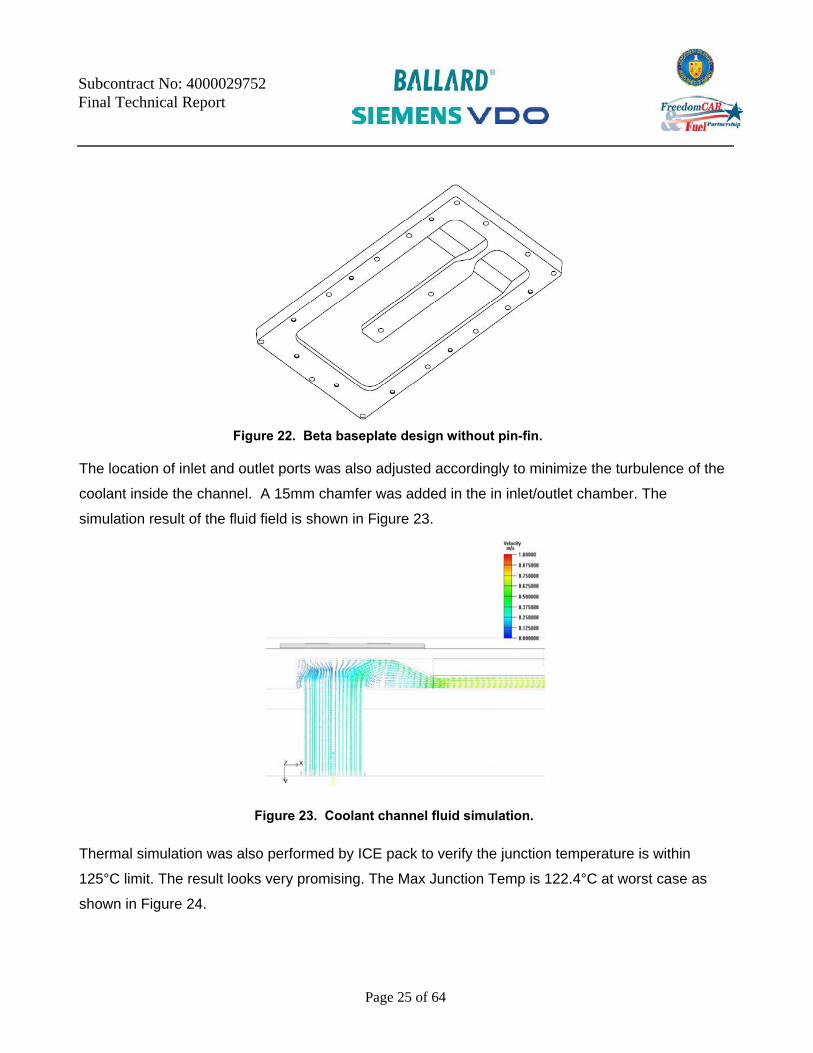
The location of inlet and outlet ports was also adjusted accordingly to minimize the turbulence of the
coolant inside the channel. A 15mm chamfer was added in the in inlet/outlet chamber. The
simulation result of the fluid field is shown in Figure 23.
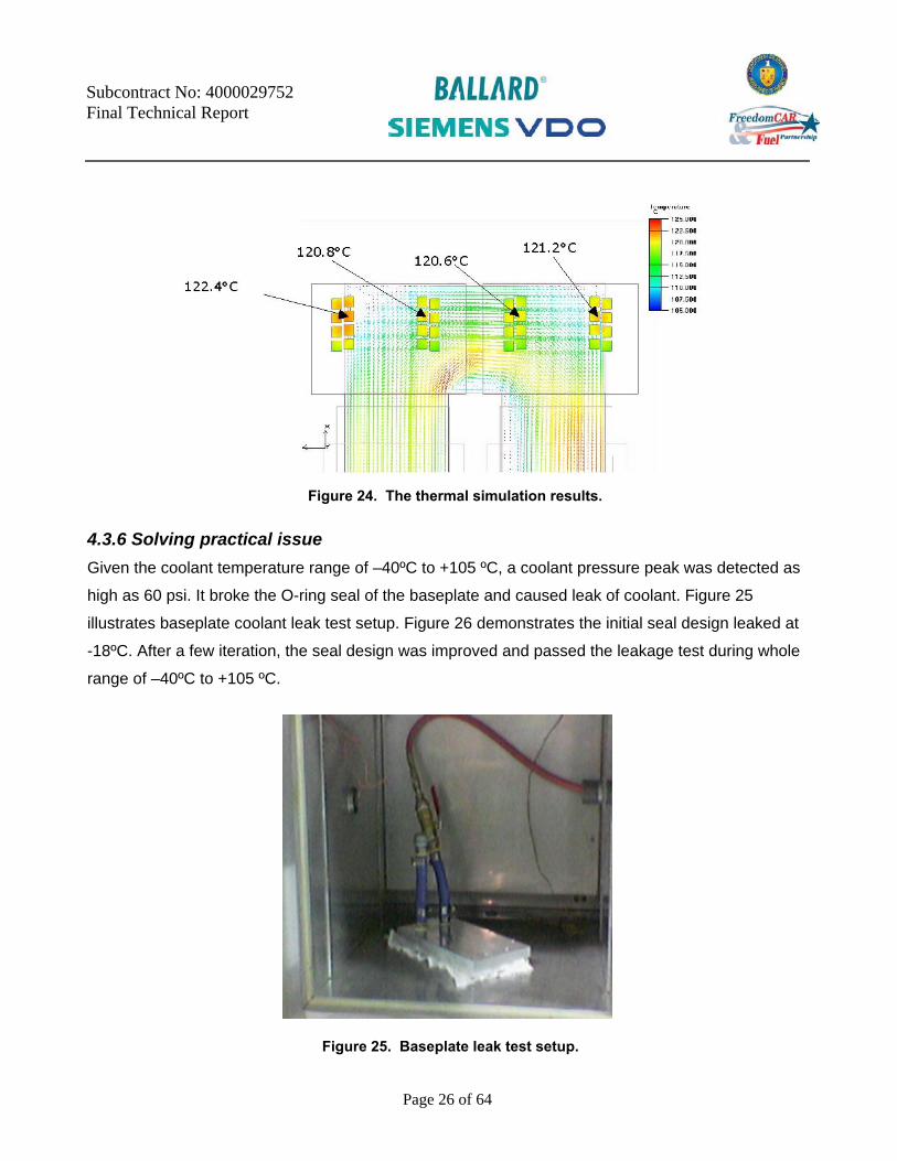
Thermal simulation was also performed by ICE pack to verify the junction temperature is within
125°C limit. The result looks very promising. The Max Junction Temp is 122.4°C at worst case as
shown in Figure 24.
Figure 22. Beta baseplate design without pin-fin.
Figure 23. Coolant channel fluid simulation.
Page 26 of 64
Subcontract No: 4000029752 Final Technical Report
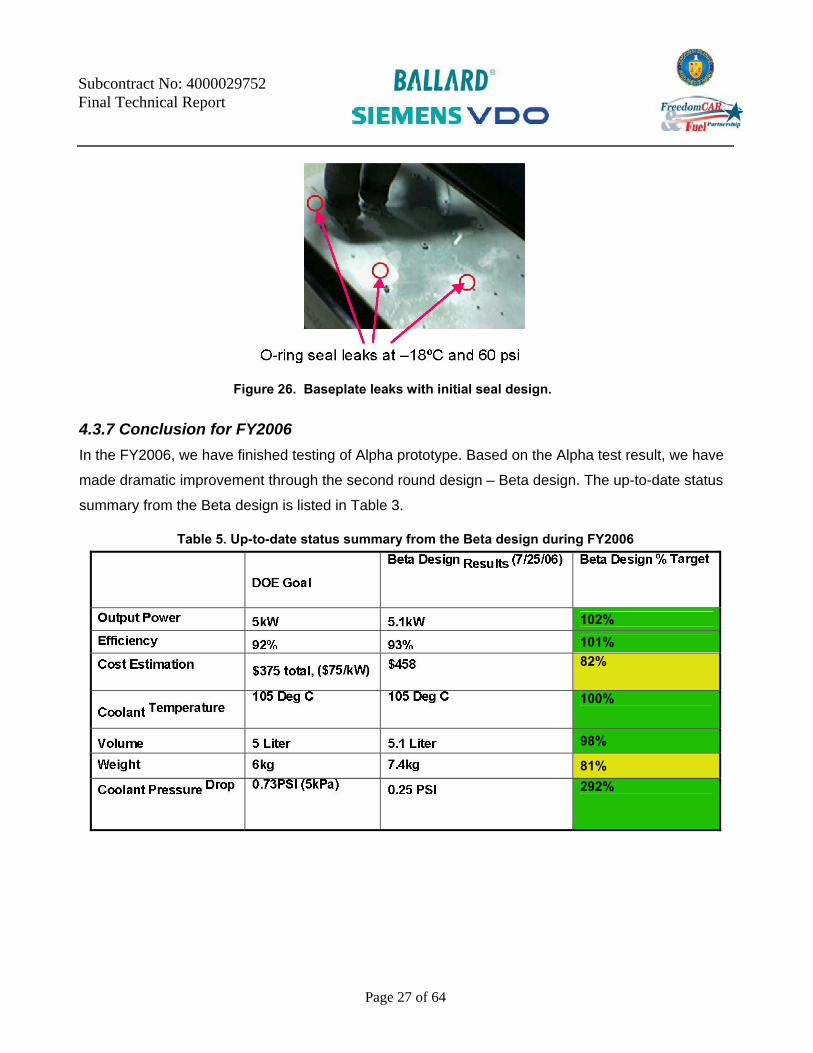
4.3.6 Solving practical issue Given the coolant temperature range of –40ºC to +105 ºC, a coolant pressure peak was detected as
high as 60 psi. It broke the O-ring seal of the baseplate and caused leak of coolant. Figure 25
illustrates baseplate coolant leak test setup. Figure 26 demonstrates the initial seal design leaked at
-18ºC. After a few iteration, the seal design was improved and passed the leakage test during whole
range of –40ºC to +105 ºC.
Figure 24. The thermal simulation results.
Figure 25. Baseplate leak test setup.
Page 27 of 64
Subcontract No: 4000029752 Final Technical Report
4.3.7 Conclusion for FY2006 In the FY2006, we have finished testing of Alpha prototype. Based on the Alpha test result, we have
made dramatic improvement through the second round design – Beta design. The up-to-date status
summary from the Beta design is listed in Table 3.
Table 5. Up-to-date status summary from the Beta design during FY2006
102%
101% 82%
100%
98%
81%
292%
Figure 26. Baseplate leaks with initial seal design.
Page 28 of 64
Subcontract No: 4000029752 Final Technical Report
4.4 Technical Achievements Highlights in FY2007 We have had very promising test results in the Alpha prototypes. The focus of the FY2007 is on the
manufacturing Beta prototype the final test.
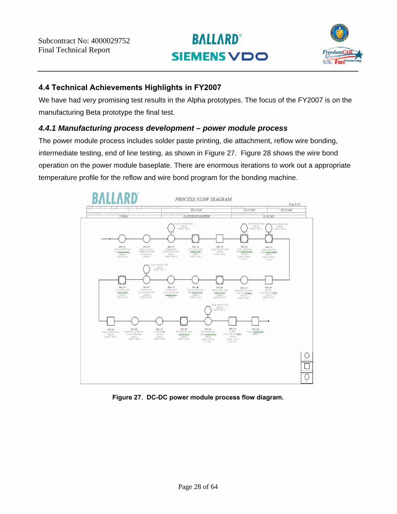
4.4.1 Manufacturing process development – power module process The power module process includes solder paste printing, die attachment, reflow wire bonding,
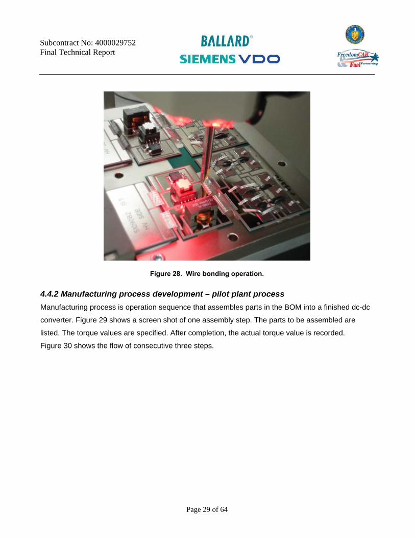
intermediate testing, end of line testing, as shown in Figure 27. Figure 28 shows the wire bond
operation on the power module baseplate. There are enormous iterations to work out a appropriate
temperature profile for the reflow and wire bond program for the bonding machine.
Figure 27. DC-DC power module process flow diagram.
Page 29 of 64
Subcontract No: 4000029752 Final Technical Report
Figure 28. Wire bonding operation.
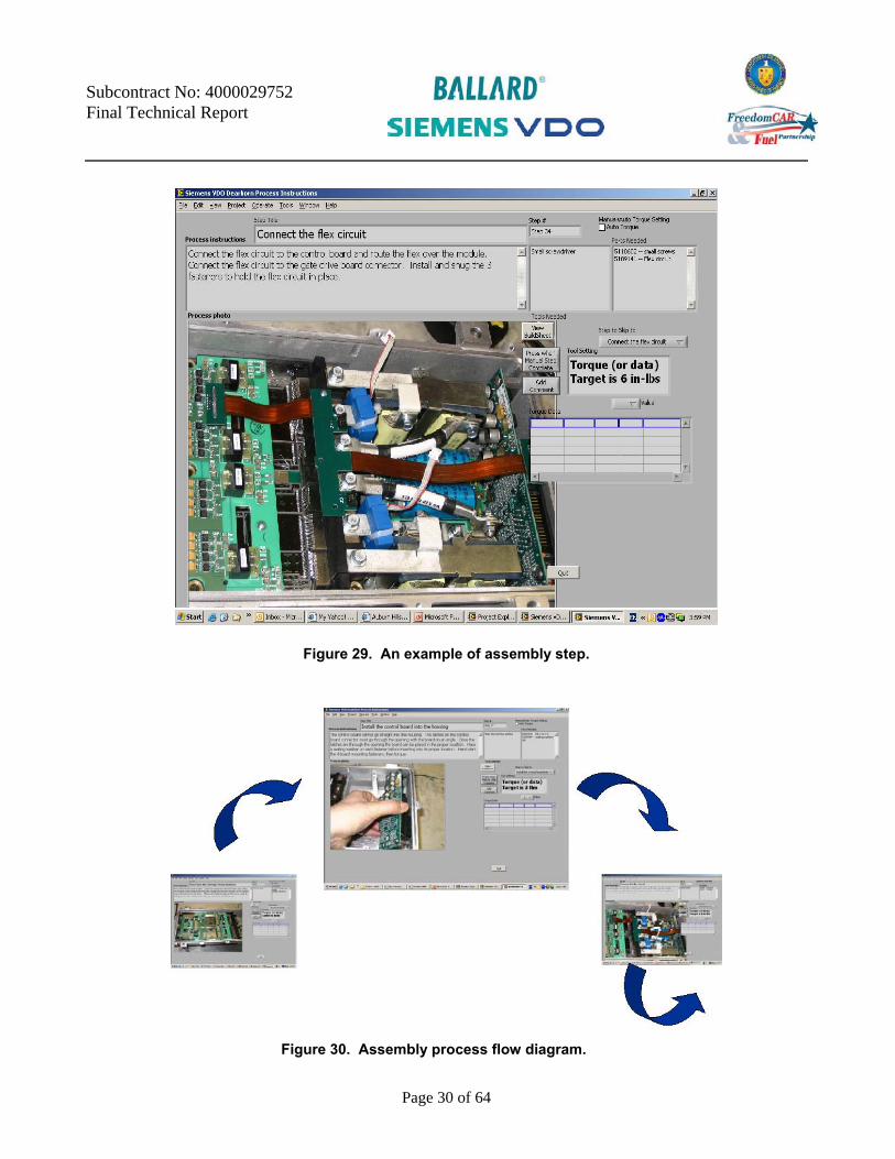
4.4.2 Manufacturing process development – pilot plant process Manufacturing process is operation sequence that assembles parts in the BOM into a finished dc-dc
converter. Figure 29 shows a screen shot of one assembly step. The parts to be assembled are
listed. The torque values are specified. After completion, the actual torque value is recorded.
Figure 30 shows the flow of consecutive three steps.
Page 30 of 64
Subcontract No: 4000029752 Final Technical Report
Figure 29. An example of assembly step.
Figure 30. Assembly process flow diagram.
Page 31 of 64
Subcontract No: 4000029752 Final Technical Report
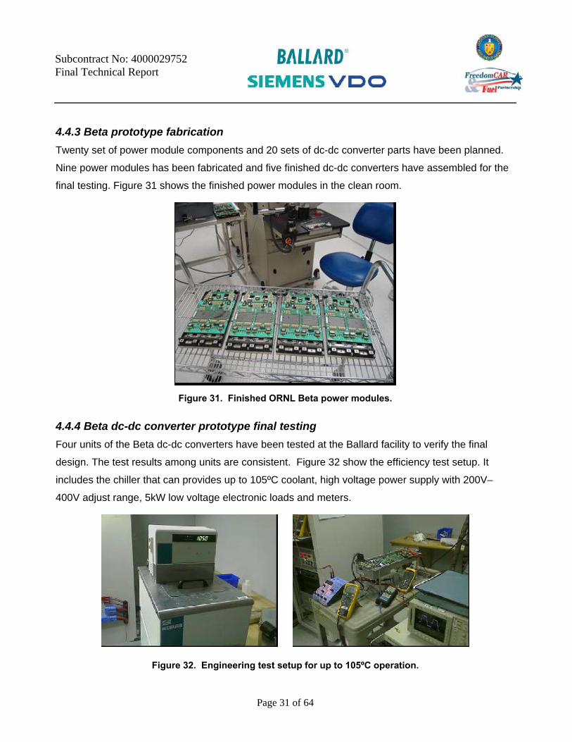
4.4.3 Beta prototype fabrication Twenty set of power module components and 20 sets of dc-dc converter parts have been planned.
Nine power modules has been fabricated and five finished dc-dc converters have assembled for the
final testing. Figure 31 shows the finished power modules in the clean room.
Figure 31. Finished ORNL Beta power modules.
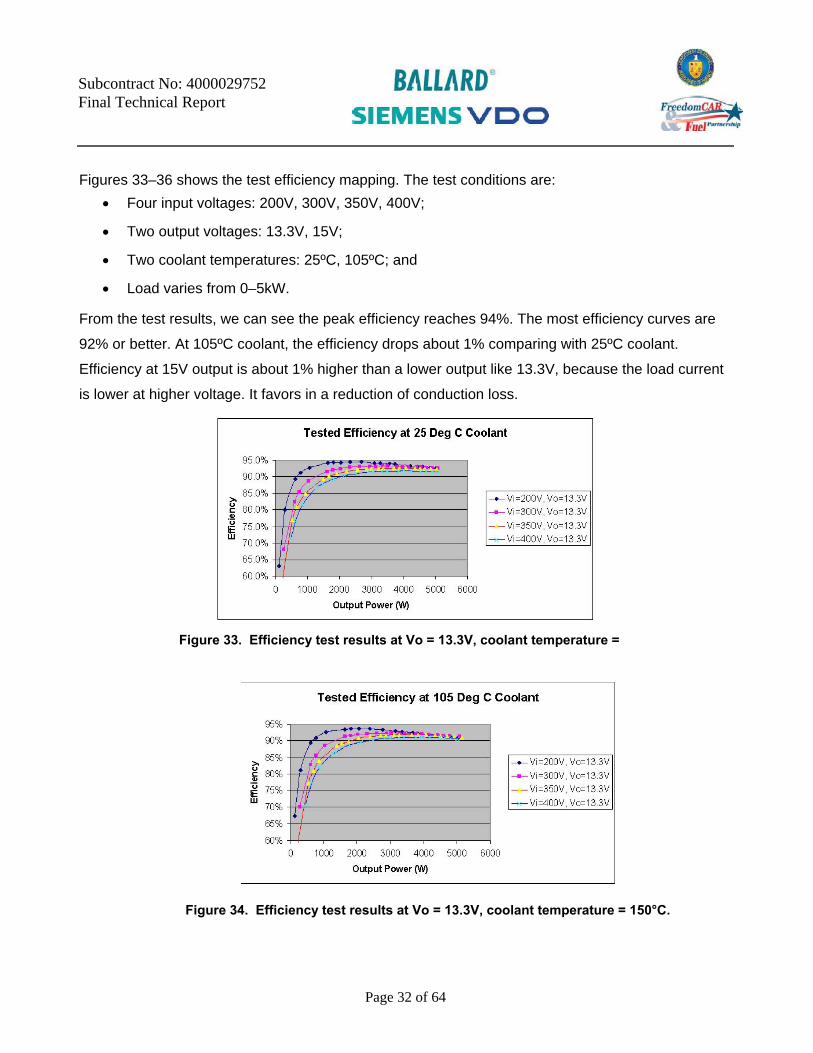
4.4.4 Beta dc-dc converter prototype final testing Four units of the Beta dc-dc converters have been tested at the Ballard facility to verify the final
design. The test results among units are consistent. Figure 32 show the efficiency test setup. It
includes the chiller that can provides up to 105ºC coolant, high voltage power supply with 200V–
400V adjust range, 5kW low voltage electronic loads and meters.
Figure 32. Engineering test setup for up to 105ºC operation.
Page 32 of 64
Subcontract No: 4000029752 Final Technical Report
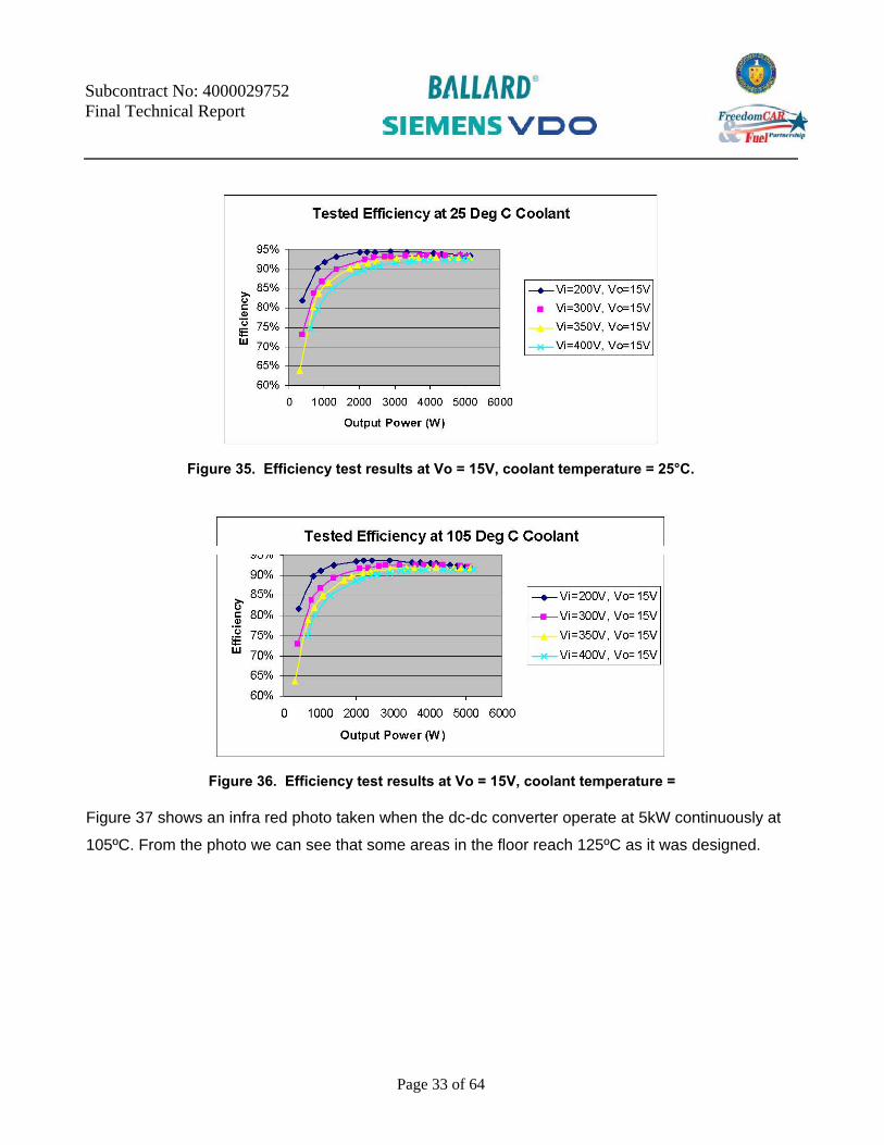
Figures 33–36 shows the test efficiency mapping. The test conditions are: • Four input voltages: 200V, 300V, 350V, 400V;
• Two output voltages: 13.3V, 15V;
• Two coolant temperatures: 25ºC, 105ºC; and
• Load varies from 0–5kW.
From the test results, we can see the peak efficiency reaches 94%. The most efficiency curves are
92% or better. At 105ºC coolant, the efficiency drops about 1% comparing with 25ºC coolant.
Efficiency at 15V output is about 1% higher than a lower output like 13.3V, because the load current
is lower at higher voltage. It favors in a reduction of conduction loss.
Figure 33. Efficiency test results at Vo = 13.3V, coolant temperature =
Figure 34. Efficiency test results at Vo = 13.3V, coolant temperature = 150°C.
Page 33 of 64
Subcontract No: 4000029752 Final Technical Report
Figure 37 shows an infra red photo taken when the dc-dc converter operate at 5kW continuously at
105ºC. From the photo we can see that some areas in the floor reach 125ºC as it was designed.
Figure 35. Efficiency test results at Vo = 15V, coolant temperature = 25°C.
Figure 36. Efficiency test results at Vo = 15V, coolant temperature =

Page 34 of 64
Subcontract No: 4000029752 Final Technical Report
5 FINAL PROGRAM REVIEW AND WITNESS TEST
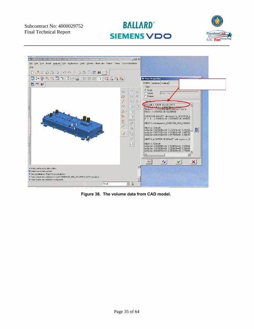
5.1 Beta Prototype Size and Dimensions Figure 38 shows the volume data from the CAD model. It reaches a total volume of 5.1 Liter, which
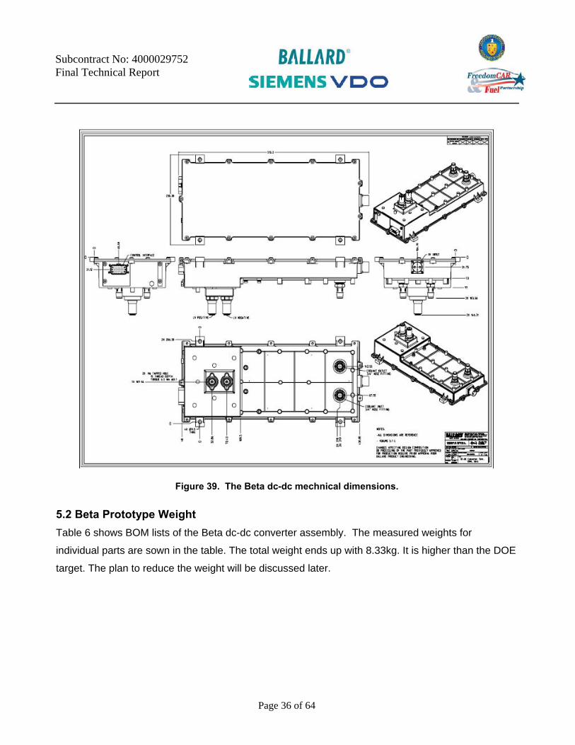
is slightly over DOE target of 5 Liter. Figure 39 depicts the dimension of the Beat prototype. It shows
four mounting tabs that can be used to mount the unit into vehicle for on-road testing.
Figure 37. A infra red photo for dc-dc converter test condition: Vi = 300V, Po = 5kW, coolant temperature = 105°C.
Page 35 of 64
Subcontract No: 4000029752 Final Technical Report
Figure 38. The volume data from CAD model.
Page 36 of 64
Subcontract No: 4000029752 Final Technical Report
Figure 39. The Beta dc-dc mechnical dimensions.
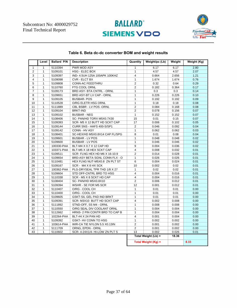
5.2 Beta Prototype Weight Table 6 shows BOM lists of the Beta dc-dc converter assembly. The measured weights for
individual parts are sown in the table. The total weight ends up with 8.33kg. It is higher than the DOE
target. The plan to reduce the weight will be discussed later.
Page 37 of 64
Subcontract No: 4000029752 Final Technical Report
Table 6. Beta dc-dc converter BOM and weight results
Level Ballard P/N Description Quantity Weight/pc (Lb) Weight Weight (Kg)
1 1 5110394 PWR MOD ASY 1 6.17 6.17 2.80 2 1 5109101 HSG - ELEC BOX 1 4.57 4.57 2.07 3 1 5109397 IND- 4.5UH 125A 100APK 100KHZ 4 0.664 2.656 1.21 4 1 5109098 CVR - ELCT BX 1 1.674 1.674 0.76 5 1 5109808 CONN-AC FEEDTHRU 2 0.32 0.64 0.29 6 1 5110760 FTG COOL ORNL 2 0.182 0.364 0.17 7 1 5109173 BRD ASY- BTA CNTRL - ORNL 1 0.3 0.3 0.14 8 1 5109651 BRD ASY-BT LV CAP - ORNL 1 0.226 0.226 0.10 9 1 5109105 BUSBAR- POS 1 0.192 0.192 0.09
10 1 5110528 O/RG ELETR HSG ORNL 1 0.18 0.18 0.08 11 1 5111889 CBL BSBR - LV POS -ORNL 2 0.084 0.168 0.08 12 1 5109104 BRKT-IND 2 0.078 0.156 0.07 13 1 5109102 BUSBAR - NEG 1 0.152 0.152 0.07 14 1 5108406 SC- PAN/HD TORX M5X0.7X30 15 0.01 0.15 0.07 15 1 5109393 SCR- M5 X 12 BUTT HD SCKT CAP 17 0.006 0.102 0.05 16 1 5109144 CURR SNS - HAFS 400-S/SP1 2 0.046 0.092 0.04 17 1 5109142 CONN - HV ASY 1 0.062 0.062 0.03 18 1 5108401 SC-HEX/HD M5X0.8X14 CAP FL/SPG 8 0.01 0.08 0.04 19 1 5109601 BUSBAR - LV POS 1 0.048 0.048 0.02 20 1 5109600 BUSBAR - LV POS 1 0.046 0.046 0.02 21 1 100330-PAA BLT-M4 X 0.7 X 12 CAP HD 9 0.004 0.036 0.02 22 1 103371-PAA BLT-M5 X 18 HEX SCKT CAP 4 0.008 0.032 0.01 23 1 5109511 SCR- FLNG HEX HD M6 X 16-10.9 2 0.014 0.028 0.01 24 1 5109654 BRD-ASY BETA SGNL CONN FLX - O 1 0.026 0.026 0.01 25 1 5110481 HEX FLNG NUT-M5X0.8 ZN PLT ST 6 0.004 0.024 0.01 26 1 5109167 SCR - M4 X 8 HX SCK 10 0.002 0.02 0.01 27 1 100362-PAA PLG-DRYSEAL TPR THD 1/8 X 27 1 0.02 0.02 0.01 28 1 5109604 STD OFF-CNTRL BRD TO HSG 4 0.004 0.016 0.01 29 1 5110338 SCR - M5 X 8 SCKT HD CAP 4 0.004 0.016 0.01 30 1 5108404 SC- PAN/HD M5X0.8X10 2 0.006 0.012 0.01 31 1 5109394 WSHR - SE FOR M5 SCR 12 0.001 0.012 0.01 32 1 5110407 O/RG - COOL CH 1 0.01 0.01 0.00 33 1 5110400 O/RG - COOL CH 1 0.01 0.01 0.00 34 1 5109605 GSKT-SIL GEL PAD IND BRKT 1 0.01 0.01 0.00 35 1 5109391 SCR- M3X10 BUTT HD SCKT CAP 4 0.002 0.008 0.00 36 1 5111892 STND-OFF, SS M4 - ORNL 1 0.008 0.008 0.00 37 1 5110550 O/RG SEAL DIV COOLANT ORNL 1 0.004 0.004 0.00 38 1 5112662 HRNS- 2 PIN CONTR BRD TO CAP B 1 0.004 0.004 0.00 39 1 102264-PAA BLT-#4 X 24 PAN HD 4 0.001 0.004 0.00 40 1 5109392 GSKT- HV CONN TO HSG 1 0.002 0.002 0.00 41 1 103614-PAA WIR-CA TIE NYLON 5.5 X0.13IN 2 0.001 0.002 0.00 42 1 5111709 ORNG, EPDN - ORNL 2 0.001 0.002 0.00 43 1 5110602 SCR- 4-24X1/4- HI-LOW ZN PLT S 13 0.002 0.026 0.01
Total Weight (Lb) = 18.36 Total Weight (Kg) = 8.33

Page 38 of 64
Subcontract No: 4000029752 Final Technical Report
5.3 Final Program Review and Witness Test The final program review was held on March 22, 2007 at Siemens VDO (Prior Ballard), 15001
Commerce Dr. North, Dearborn, Michigan. Ten people from USCAR EETT team joined the final
review. A facility tour was also conducted to show the Clean room, pilot plant assembly line, test
labs, and dynomometers. The review team is listed below: • Rafi Al-Attar, DCX
• Greg Smith, GM
• Franco Leonardi, Ford
• Mark Mehall, Ford
• Edward Jih, Ford
• Molly Close, DCX
• Niklas Pettersson, DCX
• Laura Marlino, ORNL
• Ray Fessler, Biztek Consulting (DOE support)
• Natalie Olds, USCAR
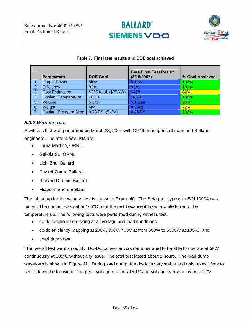
5.3.1 Final test result summary and DOE goal achieved Table 7 summaries the results that we have achieved for this program. We have achieved five of
seven goals. The weight target can also be achieved in the high volume production design. The cost
can also be improved. The opportunities to improve these two parameters will be discussed in the
later section. The coolant pressure exceeds the goal by 192% due to the effort on the thermal and
coolant channel design.
Page 39 of 64
Subcontract No: 4000029752 Final Technical Report
Table 7. Final test results and DOE goal achieved
Parameters DOE Goal
Beta Final Test Result (3/15/2007) % Goal Achieved
1 Output Power 5kW 5.1kW 102% 2 Efficiency 92% 93% 101% 3 Cost Estimation $375 total, ($75/kW) $458 82% 3 Coolant Temperature 105 ºC 105 ºC 100% 5 Volume 5 Liter 5.1 Liter 98% 6 Weight 6kg 8.33kg 72% 7 Coolant Pressure Drop 0.73 PSI (5kPa) 0.25 PSI 292%
5.3.2 Witness test A witness test was performed on March 23, 2007 with ORNL management team and Ballard
engineers. The attendee's lists are: • Laura Marlino, ORNL
• Gui-Jia Su, ORNL
• Lizhi Zhu, Ballard
• Dawud Zama, Ballard
• Richard Debbin, Ballard
• Miaosen Shen, Ballard
The lab setup for the witness test is shown in Figure 40. The Beta prototype with S/N 10004 was
tested. The coolant was set at 105ºC prior the test because it takes a while to ramp the
temperature up. The following tests were performed during witness test. • dc-dc functional checking at all voltage and load conditions;
• dc-dc efficiency mapping at 200V, 300V, 400V at from 600W to 5000W at 105ºC; and
• Load dump test.
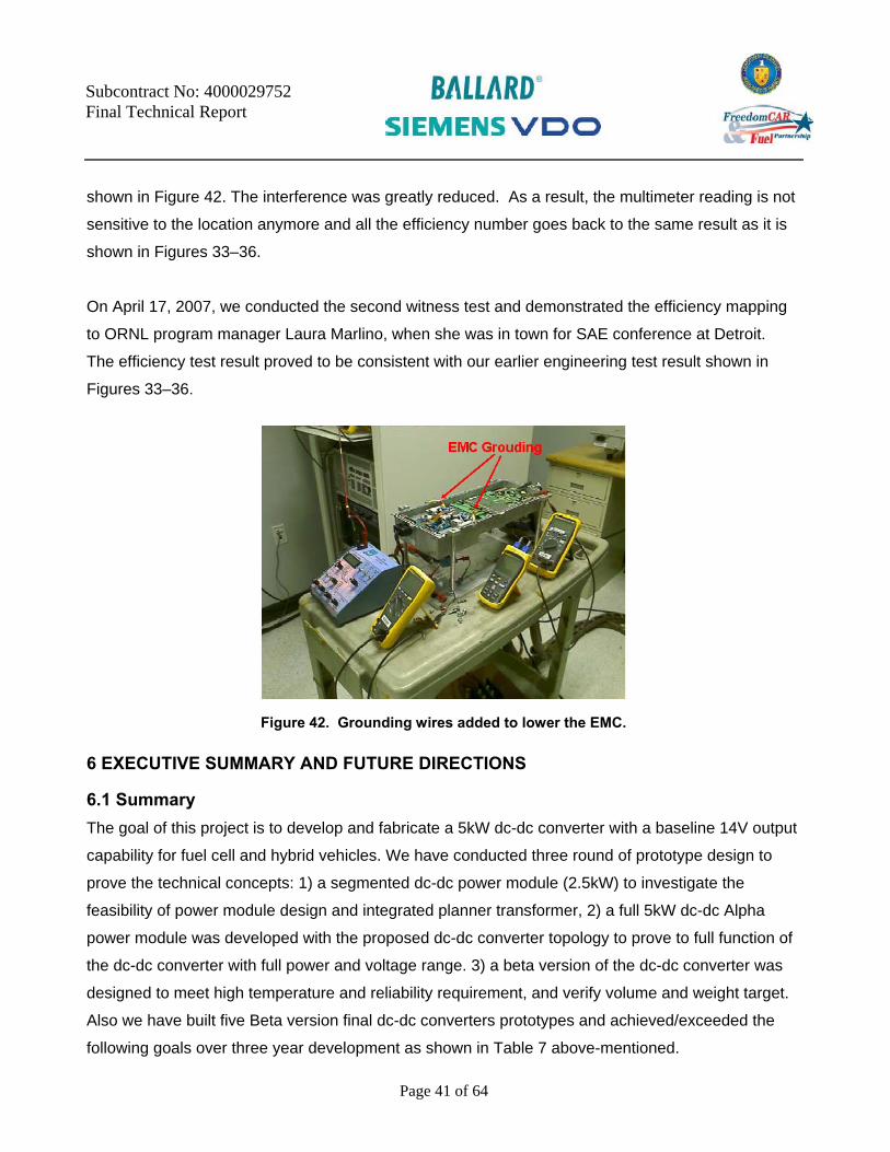
The overall test went smoothly. DC-DC converter was demonstrated to be able to operate at 5kW
continuously at 105ºC without any issue. The total test lasted about 2 hours. The load dump
waveform is shown in Figure 41. During load dump, the dc-dc is very stable and only takes 15ms to
settle down the transient. The peak voltage reaches 15.1V and voltage overshoot is only 1.7V.
Page 40 of 64
Subcontract No: 4000029752 Final Technical Report
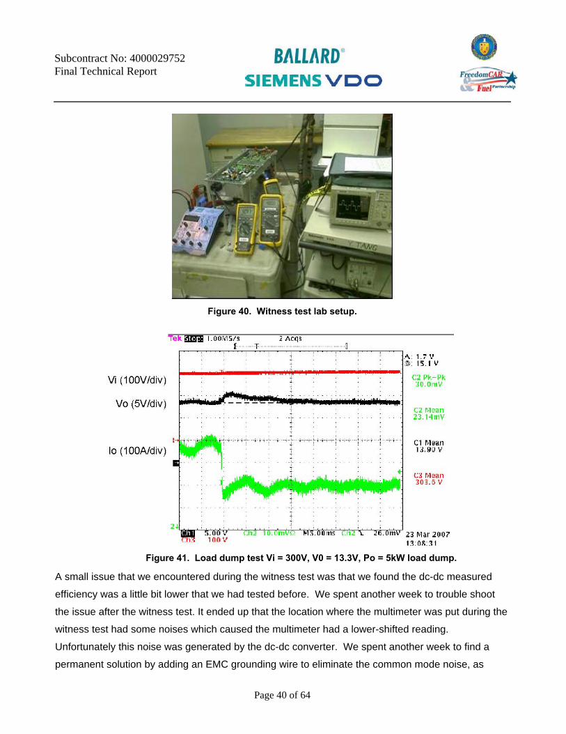
Figure 40. Witness test lab setup.
A small issue that we encountered during the witness test was that we found the dc-dc measured
efficiency was a little bit lower that we had tested before. We spent another week to trouble shoot
the issue after the witness test. It ended up that the location where the multimeter was put during the
witness test had some noises which caused the multimeter had a lower-shifted reading.
Unfortunately this noise was generated by the dc-dc converter. We spent another week to find a
permanent solution by adding an EMC grounding wire to eliminate the common mode noise, as
Figure 41. Load dump test Vi = 300V, V0 = 13.3V, Po = 5kW load dump.
Page 41 of 64
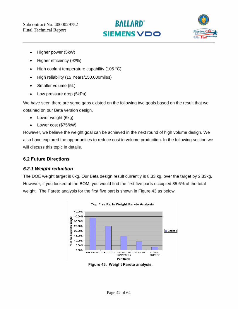
Subcontract No: 4000029752 Final Technical Report
shown in Figure 42. The interference was greatly reduced. As a result, the multimeter reading is not
sensitive to the location anymore and all the efficiency number goes back to the same result as it is
shown in Figures 33–36.
On April 17, 2007, we conducted the second witness test and demonstrated the efficiency mapping
to ORNL program manager Laura Marlino, when she was in town for SAE conference at Detroit.
The efficiency test result proved to be consistent with our earlier engineering test result shown in
Figures 33–36.
6 EXECUTIVE SUMMARY AND FUTURE DIRECTIONS
6.1 Summary The goal of this project is to develop and fabricate a 5kW dc-dc converter with a baseline 14V output
capability for fuel cell and hybrid vehicles. We have conducted three round of prototype design to
prove the technical concepts: 1) a segmented dc-dc power module (2.5kW) to investigate the
feasibility of power module design and integrated planner transformer, 2) a full 5kW dc-dc Alpha
power module was developed with the proposed dc-dc converter topology to prove to full function of
the dc-dc converter with full power and voltage range. 3) a beta version of the dc-dc converter was
designed to meet high temperature and reliability requirement, and verify volume and weight target.
Also we have built five Beta version final dc-dc converters prototypes and achieved/exceeded the
following goals over three year development as shown in Table 7 above-mentioned.
Figure 42. Grounding wires added to lower the EMC.
Page 42 of 64
Subcontract No: 4000029752 Final Technical Report
• Higher power (5kW)
• Higher efficiency (92%)
• High coolant temperature capability (105 °C)
• High reliability (15 Years/150,000miles)
• Smaller volume (5L)
• Low pressure drop (5kPa)
We have seen there are some gaps existed on the following two goals based on the result that we
obtained on our Beta version design.
• Lower weight (6kg)
• Lower cost ($75/kW)
However, we believe the weight goal can be achieved in the next round of high volume design. We
also have explored the opportunities to reduce cost in volume production. In the following section we
will discuss this topic in details.
6.2 Future Directions
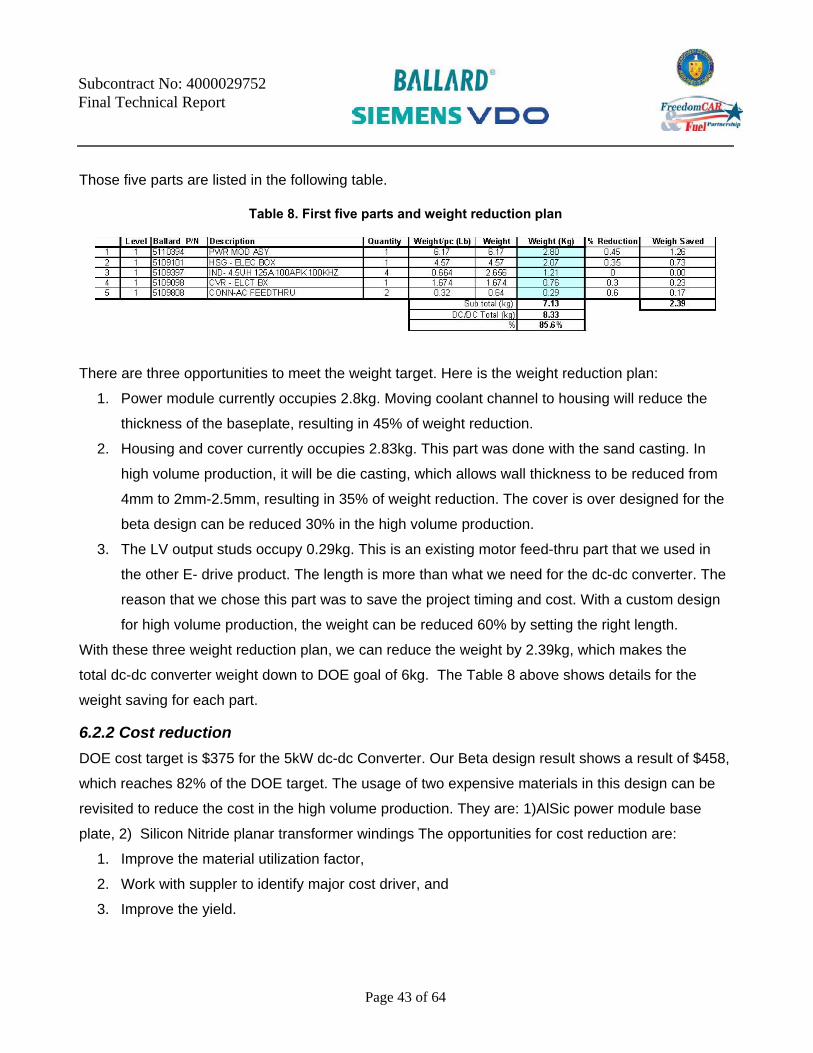
6.2.1 Weight reduction The DOE weight target is 6kg. Our Beta design result currently is 8.33 kg, over the target by 2.33kg.
However, if you looked at the BOM, you would find the first five parts occupied 85.6% of the total
weight. The Pareto analysis for the first five part is shown in Figure 43 as below.
Figure 43. Weight Pareto analysis.
Page 43 of 64
Subcontract No: 4000029752 Final Technical Report
Those five parts are listed in the following table.
Table 8. First five parts and weight reduction plan
There are three opportunities to meet the weight target. Here is the weight reduction plan:
1. Power module currently occupies 2.8kg. Moving coolant channel to housing will reduce the
thickness of the baseplate, resulting in 45% of weight reduction.
2. Housing and cover currently occupies 2.83kg. This part was done with the sand casting. In
high volume production, it will be die casting, which allows wall thickness to be reduced from
4mm to 2mm-2.5mm, resulting in 35% of weight reduction. The cover is over designed for the
beta design can be reduced 30% in the high volume production.
3. The LV output studs occupy 0.29kg. This is an existing motor feed-thru part that we used in
the other E- drive product. The length is more than what we need for the dc-dc converter. The
reason that we chose this part was to save the project timing and cost. With a custom design
for high volume production, the weight can be reduced 60% by setting the right length.
With these three weight reduction plan, we can reduce the weight by 2.39kg, which makes the
total dc-dc converter weight down to DOE goal of 6kg. The Table 8 above shows details for the
weight saving for each part.
6.2.2 Cost reduction DOE cost target is $375 for the 5kW dc-dc Converter. Our Beta design result shows a result of $458,
which reaches 82% of the DOE target. The usage of two expensive materials in this design can be
revisited to reduce the cost in the high volume production. They are: 1)AlSic power module base
plate, 2) Silicon Nitride planar transformer windings The opportunities for cost reduction are:
1. Improve the material utilization factor,
2. Work with suppler to identify major cost driver, and
3. Improve the yield.
Page 44 of 64
Subcontract No: 4000029752 Final Technical Report
7 Publications 1) Presentation on USCAR meeting, Southfield, MI, March 30, 2006.
2) Presentation on 2006 DOE FreedomCAR APEEM Annual Review, Pollard Technology
Conference Center, Oak Ridge, Tennessee, August 16, 2006.
3) Presentation on Industrial Power Converter Products and Services Session in IEEE IAS 2006,
Tampa, FL, October 12, 2006.
4) "An Interleaved High Power dc-dc Converter,” US Patent Application No. 20050270806.
5) "Integration of Planar Magnetics Transformer and Power Switching Devices in a Liquid-cooled
High Power dc-dc Converter," Patent Application No. 20050270745.

Page 45 of 64
APPENDIX: ORNL Test Verification To verify the efficiency maps, previously measured by Ballard, tests were done on March 23, 2007 witnessed
by ORNL representatives. Laura Marlino and Gui Jia Su were in attendance. Ballard was represented by Lizhi
Zhu (PI), Miaoshen Shen (Power Electronics Engineer), Richard DeBin (Test Engineer), and David Zama
(Mechanical Packaging Engineer).
All measurement equipment utilized during the testing was verified to be within their calibration dates. No
computerized data acquisition system or power meters were used during the testing. All measurements were
taken with DVMs and oscilloscopes. Data was then entered into a spreadsheet manually and efficiency
calculations derived from the entries.
The unit was tested in the open air in the laboratory at approximately 25°C. The top of the unit was removed
to allow probes to be inserted at the test points. The coolant was heated to 105°C and allowed to circulate
through the unit. A thermocouple was used to measure the housing temperature and was placed on the
underside of the unit near the coolant inlet. The unit was elevated in the air on standoffs for the tests. The
testing included capturing efficiency data at different power and voltage levels, measuring the unit’s line and
load regulation and its dynamic response.
Due to time constraints verification points were chosen at approximately 10% of rated load, maximum
efficiency load, rated load, and only one or two points in between. Figures A.1(a)–(c) compare measured
efficiency points on March 23rd with those previously taken by Ballard, where the output voltage reference,
Voref, was set at 13.3V while the input voltage, Vi was adjusted precisely at 200V, 300V, and 400V,
respectively. Tests were repeated with the output voltage commanded to be 15V and the results are shown in
Figures A.2(a)–(c).
Page 46 of 64
Measured Efficiency at 105 Deg C Coolant (Voref=13.3V)
60%
65%
70%
75%
80%
85%
90%
95%
0.0 1000.0 2000.0 3000.0 4000.0 5000.0 6000.0Output Power (W)
Effi
cien
cy
Vi=200V (ORNL Witnessed)Vi=200VSpecs-Minimum Efficiency Line
Figure A.1(a). Input voltage at 200V.
Measured Efficiency at 105 Deg C Coolant (Voref=13.3V)
70%
75%
80%
85%
90%
95%
0.0 1000.0 2000.0 3000.0 4000.0 5000.0 6000.0Output Power (W)
Effi
cien
cy
Vi=300V (ORNL Witnessed)Vi=300VSpecs-Minimum Efficiency Line
Figure A.1(b). Input voltage at 300V.
Page 47 of 64
Measured Efficiency at 105 Deg C Coolant (Voref=13.3V)
60%
65%
70%
75%
80%
85%
90%
95%
0.0 1000.0 2000.0 3000.0 4000.0 5000.0 6000.0Output Power (W)
Effi
cien
cy
Vi=400V (ORNL Witnessed)Vi=400VSpecs-Minimum Efficiency Line
Figure A.1(c). Input voltage at 400V.
Measured Efficiency at 105 Deg C Coolant (Voref=15V)
70%
75%
80%
85%
90%
95%
0.0 1000.0 2000.0 3000.0 4000.0 5000.0 6000.0Output Power (W)
Effi
cien
cy
Vi=200V (ORNL Witnessed)Vi=200VSpecs-Minimum Efficiency Line
Figure A.2(a). Input voltage at 200V.
Page 48 of 64
Measured Efficiency at 105 Deg C Coolant (Voref=15V)
70%
75%
80%
85%
90%
95%
0.0 1000.0 2000.0 3000.0 4000.0 5000.0 6000.0Output Power (W)
Effi
cien
cy
Vi=300V (ORNL Witnessed)Vi=300VSpecs-Minimum Efficiency Line
Figure A.2(b). Input voltage at 300V.
Measured Efficiency at 105 Deg C Coolant (Voref=15V)
70%
75%
80%
85%
90%
95%
0.0 1000.0 2000.0 3000.0 4000.0 5000.0 6000.0Output Power (W)
Effi
cien
cy
Vi=400V (ORNL Witnessed)Vi=400VSpecs-Minimum Efficiency Line
Figure A.2(c). Input voltage at 400V.
Page 49 of 64
The tests indicate the efficiency numbers are similar to those measured by Ballard at Vi = 200V, but drop as Vi
increases in both cases of Voref. The data taken on March 23rd was taken on the identical unit that Ballard had
previously tested and it was hypothesized that the controller might be the cause of the different results.
In order to compare the test data with the efficiency specification, which states that it should be higher than
92% for loads greater than 40%, the minimum efficiency line is drawn in Figures A.1 and A.2. The best case
was obtained in Figure A.2(a), where the efficiency exceeds the specification over a wider load range.
Figures A.1(a) and A.2(b) partially meet the specification while the others do not cross the line at all.
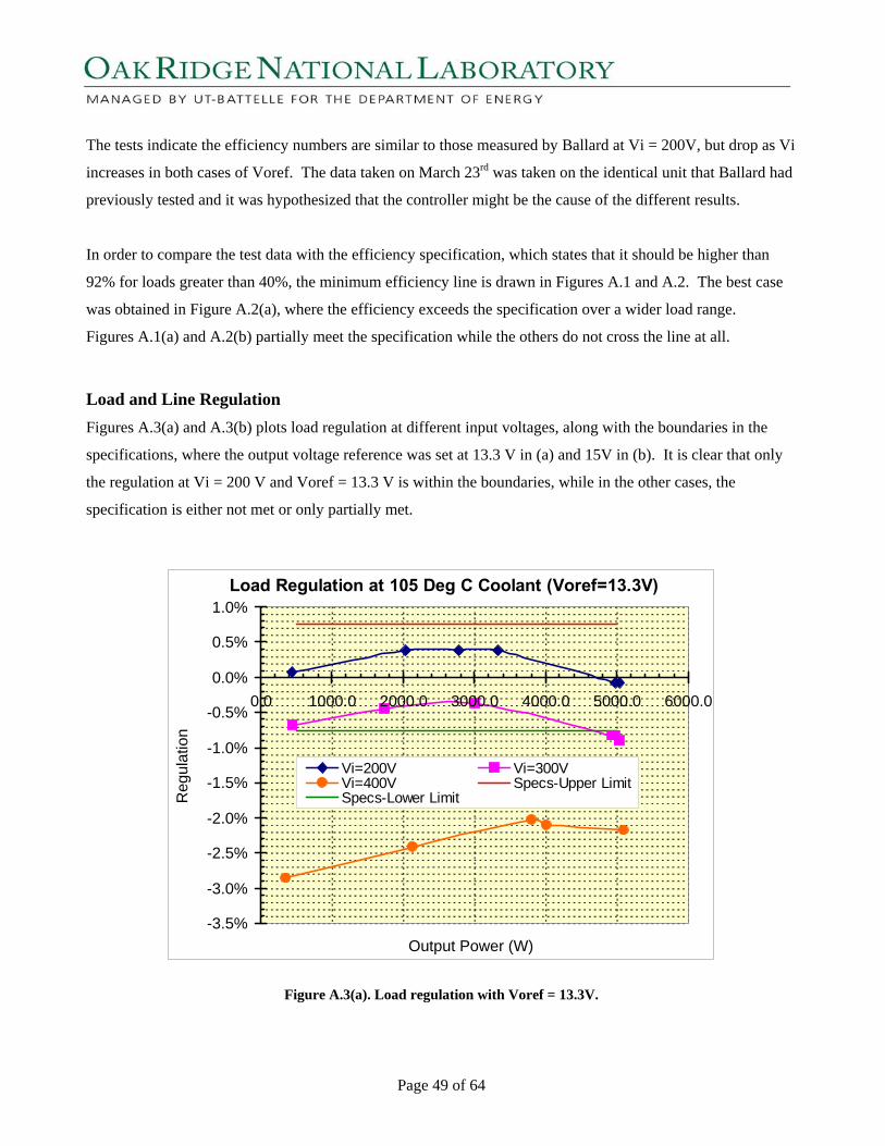
Load and Line Regulation Figures A.3(a) and A.3(b) plots load regulation at different input voltages, along with the boundaries in the
specifications, where the output voltage reference was set at 13.3 V in (a) and 15V in (b). It is clear that only
the regulation at Vi = 200 V and Voref = 13.3 V is within the boundaries, while in the other cases, the
specification is either not met or only partially met.
Load Regulation at 105 Deg C Coolant (Voref=13.3V)
-3.5%
-3.0%
-2.5%
-2.0%
-1.5%
-1.0%
-0.5%
0.0%
0.5%
1.0%
0.0 1000.0 2000.0 3000.0 4000.0 5000.0 6000.0
Output Power (W)
Reg
ulat
ion
Vi=200V Vi=300VVi=400V Specs-Upper LimitSpecs-Lower Limit
Figure A.3(a). Load regulation with Voref = 13.3V.
Page 50 of 64
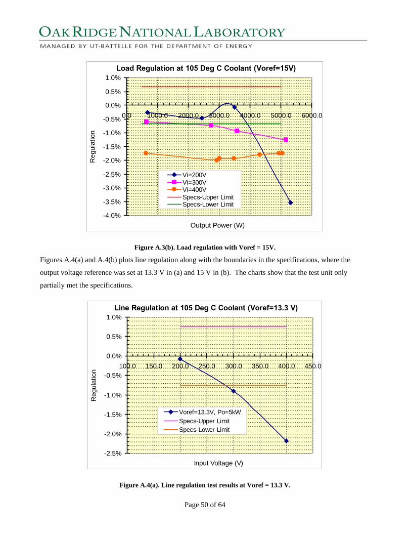
Load Regulation at 105 Deg C Coolant (Voref=15V)
-4.0%
-3.5%
-3.0%
-2.5%
-2.0%
-1.5%
-1.0%
-0.5%
0.0%
0.5%
1.0%
0.0 1000.0 2000.0 3000.0 4000.0 5000.0 6000.0
Output Power (W)
Reg
ulat
ion
Vi=200VVi=300VVi=400VSpecs-Upper LimitSpecs-Lower Limit
Figure A.3(b). Load regulation with Voref = 15V.
Figures A.4(a) and A.4(b) plots line regulation along with the boundaries in the specifications, where the
output voltage reference was set at 13.3 V in (a) and 15 V in (b). The charts show that the test unit only
partially met the specifications.
Line Regulation at 105 Deg C Coolant (Voref=13.3 V)
-2.5%
-2.0%
-1.5%
-1.0%
-0.5%
0.0%
0.5%
1.0%
100.0 150.0 200.0 250.0 300.0 350.0 400.0 450.0
Input Voltage (V)
Reg
ulat
ion
Voref=13.3V, Po=5kWSpecs-Upper LimitSpecs-Lower Limit
Figure A.4(a). Line regulation test results at Voref = 13.3 V.
Page 51 of 64
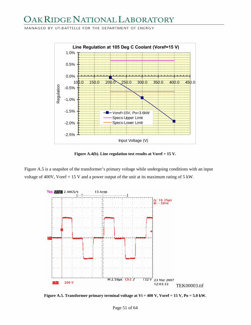
Line Regulation at 105 Deg C Coolant (Voref=15 V)
-2.5%
-2.0%
-1.5%
-1.0%
-0.5%
0.0%
0.5%
1.0%
100.0 150.0 200.0 250.0 300.0 350.0 400.0 450.0
Input Voltage (V)
Reg
ulat
ion
Voref=15V, Po=3.6kWSpecs-Upper LimitSpecs-Lower Limit
Figure A.4(b). Line regulation test results at Voref = 15 V.
Figure A.5 is a snapshot of the transformer’s primary voltage while undergoing conditions with an input
voltage of 400V, Voref = 15 V and a power output of the unit at its maximum rating of 5 kW.
TEK00003.tif
Figure A.5. Transformer primary terminal voltage at Vi = 400 V, Voref = 15 V, Po = 5.0 kW.
Page 52 of 64
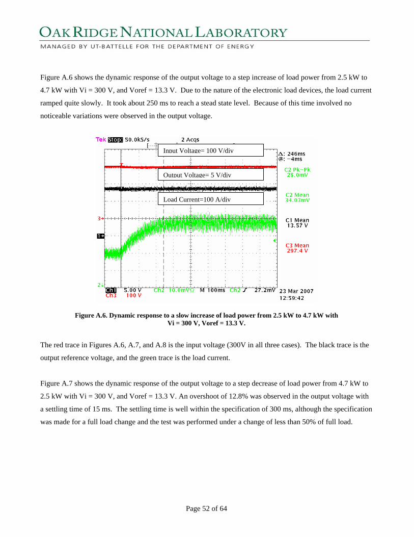
Figure A.6 shows the dynamic response of the output voltage to a step increase of load power from 2.5 kW to
4.7 kW with Vi = 300 V, and Voref = 13.3 V. Due to the nature of the electronic load devices, the load current
ramped quite slowly. It took about 250 ms to reach a stead state level. Because of this time involved no
noticeable variations were observed in the output voltage.
Figure A.6. Dynamic response to a slow increase of load power from 2.5 kW to 4.7 kW with Vi = 300 V, Voref = 13.3 V.
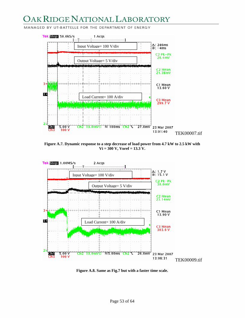
The red trace in Figures A.6, A.7, and A.8 is the input voltage (300V in all three cases). The black trace is the
output reference voltage, and the green trace is the load current.
Figure A.7 shows the dynamic response of the output voltage to a step decrease of load power from 4.7 kW to
2.5 kW with Vi = 300 V, and Voref = 13.3 V. An overshoot of 12.8% was observed in the output voltage with
a settling time of 15 ms. The settling time is well within the specification of 300 ms, although the specification
was made for a full load change and the test was performed under a change of less than 50% of full load.
Input Voltage= 100 V/div
Output Voltage= 5 V/div
Load Current=100 A/div
Page 53 of 64
TEK00007.tif
Figure A.7. Dynamic response to a step decrease of load power from 4.7 kW to 2.5 kW with Vi = 300 V, Voref = 13.3 V.
TEK00009.tif
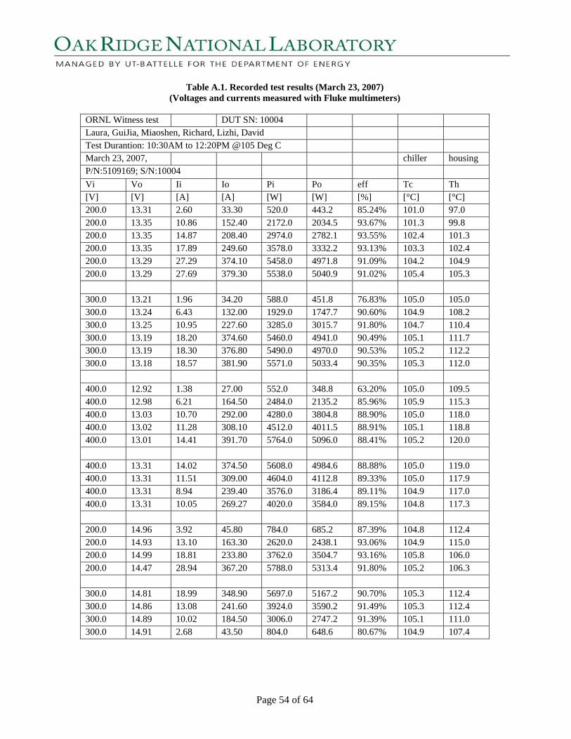
Figure A.8. Same as Fig.7 but with a faster time scale.
Output Voltage= 5 V/div
Input Voltage= 100 V/div
Load Current= 100 A/div
Input Voltage= 100 V/div
Output Voltage= 5 V/div
Load Current= 100 A/div
Page 54 of 64
Table A.1. Recorded test results (March 23, 2007) (Voltages and currents measured with Fluke multimeters)
ORNL Witness test DUT SN: 10004 Laura, GuiJia, Miaoshen, Richard, Lizhi, David Test Durantion: 10:30AM to 12:20PM @105 Deg C March 23, 2007, chiller housing P/N:5109169; S/N:10004 Vi Vo Ii Io Pi Po eff Tc Th [V] [V] [A] [A] [W] [W] [%] [°C] [°C] 200.0 13.31 2.60 33.30 520.0 443.2 85.24% 101.0 97.0 200.0 13.35 10.86 152.40 2172.0 2034.5 93.67% 101.3 99.8 200.0 13.35 14.87 208.40 2974.0 2782.1 93.55% 102.4 101.3 200.0 13.35 17.89 249.60 3578.0 3332.2 93.13% 103.3 102.4 200.0 13.29 27.29 374.10 5458.0 4971.8 91.09% 104.2 104.9 200.0 13.29 27.69 379.30 5538.0 5040.9 91.02% 105.4 105.3 300.0 13.21 1.96 34.20 588.0 451.8 76.83% 105.0 105.0 300.0 13.24 6.43 132.00 1929.0 1747.7 90.60% 104.9 108.2 300.0 13.25 10.95 227.60 3285.0 3015.7 91.80% 104.7 110.4 300.0 13.19 18.20 374.60 5460.0 4941.0 90.49% 105.1 111.7 300.0 13.19 18.30 376.80 5490.0 4970.0 90.53% 105.2 112.2 300.0 13.18 18.57 381.90 5571.0 5033.4 90.35% 105.3 112.0 400.0 12.92 1.38 27.00 552.0 348.8 63.20% 105.0 109.5 400.0 12.98 6.21 164.50 2484.0 2135.2 85.96% 105.9 115.3 400.0 13.03 10.70 292.00 4280.0 3804.8 88.90% 105.0 118.0 400.0 13.02 11.28 308.10 4512.0 4011.5 88.91% 105.1 118.8 400.0 13.01 14.41 391.70 5764.0 5096.0 88.41% 105.2 120.0 400.0 13.31 14.02 374.50 5608.0 4984.6 88.88% 105.0 119.0 400.0 13.31 11.51 309.00 4604.0 4112.8 89.33% 105.0 117.9 400.0 13.31 8.94 239.40 3576.0 3186.4 89.11% 104.9 117.0 400.0 13.31 10.05 269.27 4020.0 3584.0 89.15% 104.8 117.3 200.0 14.96 3.92 45.80 784.0 685.2 87.39% 104.8 112.4 200.0 14.93 13.10 163.30 2620.0 2438.1 93.06% 104.9 115.0 200.0 14.99 18.81 233.80 3762.0 3504.7 93.16% 105.8 106.0 200.0 14.47 28.94 367.20 5788.0 5313.4 91.80% 105.2 106.3 300.0 14.81 18.99 348.90 5697.0 5167.2 90.70% 105.3 112.4 300.0 14.86 13.08 241.60 3924.0 3590.2 91.49% 105.3 112.4 300.0 14.89 10.02 184.50 3006.0 2747.2 91.39% 105.1 111.0 300.0 14.91 2.68 43.50 804.0 648.6 80.67% 104.9 107.4
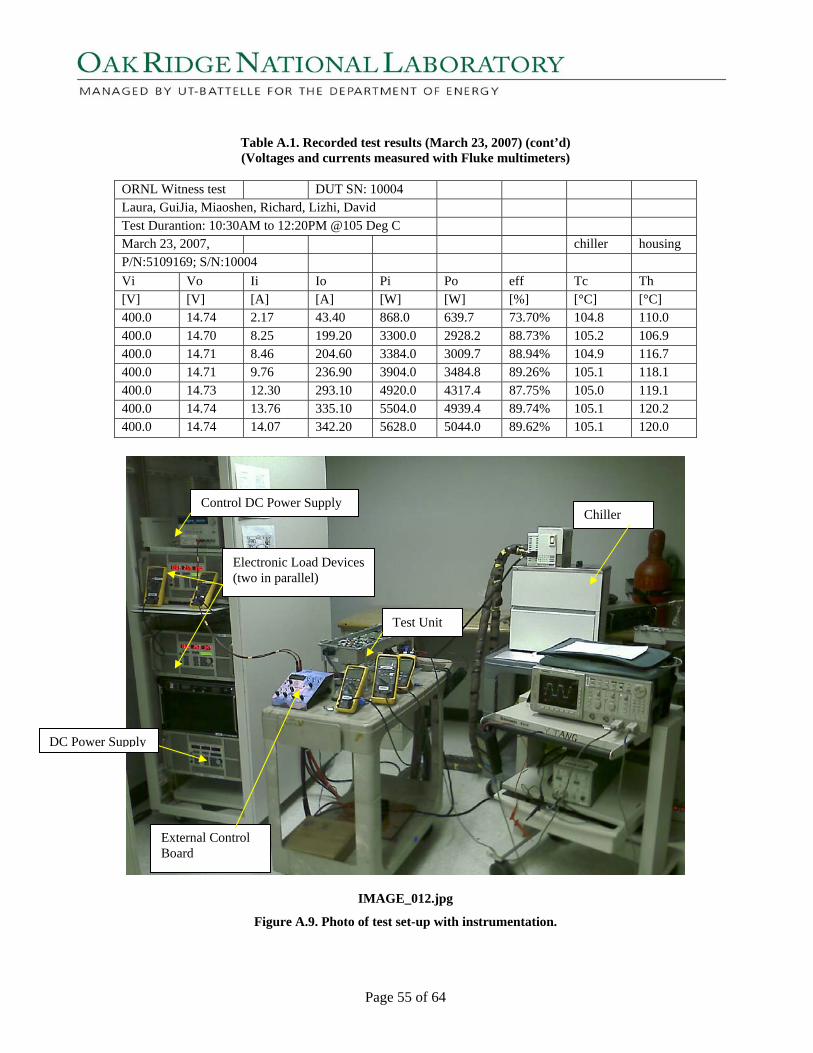
Page 55 of 64
Table A.1. Recorded test results (March 23, 2007) (cont’d) (Voltages and currents measured with Fluke multimeters)
ORNL Witness test DUT SN: 10004 Laura, GuiJia, Miaoshen, Richard, Lizhi, David Test Durantion: 10:30AM to 12:20PM @105 Deg C March 23, 2007, chiller housing P/N:5109169; S/N:10004 Vi Vo Ii Io Pi Po eff Tc Th [V] [V] [A] [A] [W] [W] [%] [°C] [°C] 400.0 14.74 2.17 43.40 868.0 639.7 73.70% 104.8 110.0 400.0 14.70 8.25 199.20 3300.0 2928.2 88.73% 105.2 106.9 400.0 14.71 8.46 204.60 3384.0 3009.7 88.94% 104.9 116.7 400.0 14.71 9.76 236.90 3904.0 3484.8 89.26% 105.1 118.1 400.0 14.73 12.30 293.10 4920.0 4317.4 87.75% 105.0 119.1 400.0 14.74 13.76 335.10 5504.0 4939.4 89.74% 105.1 120.2 400.0 14.74 14.07 342.20 5628.0 5044.0 89.62% 105.1 120.0
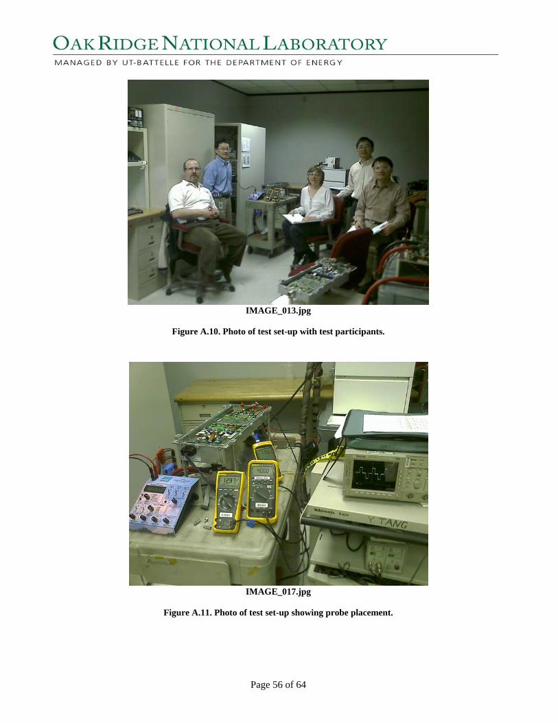
IMAGE_012.jpg
Figure A.9. Photo of test set-up with instrumentation.
Control DC Power Supply
Electronic Load Devices (two in parallel)
Test Unit
Chiller
External Control Board
DC Power Supply
Page 56 of 64
IMAGE_013.jpg
Figure A.10. Photo of test set-up with test participants.
IMAGE_017.jpg
Figure A.11. Photo of test set-up showing probe placement.
Page 57 of 64
IMAGE_018.jpg
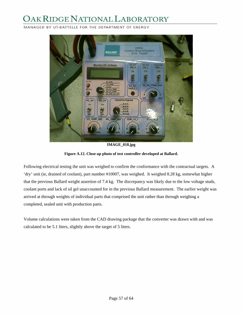
Figure A.12. Close up photo of test controller developed at Ballard.
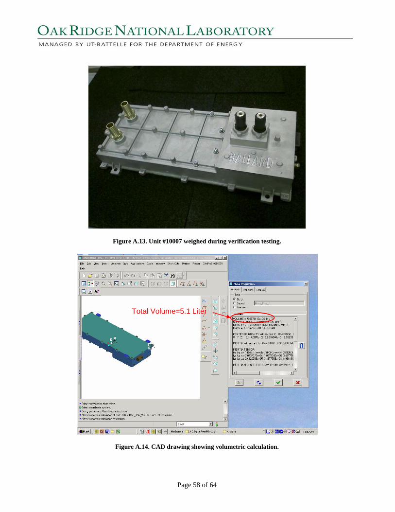
Following electrical testing the unit was weighed to confirm the conformance with the contractual targets. A
‘dry’ unit (ie, drained of coolant), part number #10007, was weighed. It weighed 8.28 kg, somewhat higher
that the previous Ballard weight assertion of 7.4 kg. The discrepancy was likely due to the low voltage studs,
coolant ports and lack of sil gel unaccounted for in the previous Ballard measurement. The earlier weight was
arrived at through weights of individual parts that comprised the unit rather than through weighing a
completed, sealed unit with production parts.
Volume calculations were taken from the CAD drawing package that the converter was drawn with and was
calculated to be 5.1 liters, slightly above the target of 5 liters.
Page 58 of 64
Figure A.13. Unit #10007 weighed during verification testing.
Figure A.14. CAD drawing showing volumetric calculation.
Total Volume=5.1 Liter

Page 59 of 64
Figure A.15. Mechanical drawing of unit showing dimensions. List of Test Equipment used in March 23rdTesting:
NesLab RTE-140 Chiller
Multiple Fluke 79 RMS DVMs
Tektronix TDS 754D Oscilloscope
Hewlett Packard Power Supply E3632A (0-15V, 7A)
Power Ten Instruments Power Supply (600V/33A)
(2) Dynaloads RBL 488 11-600-4000
Verification Tests April 17, 2007 Following the verification testing on March 23, 2007 the test setup at Ballard/Siemens was analyzed to
determine why the efficiency during testing was below what had previously been measured during in house
tests. Some problems with grounding of the unit were uncovered. It was decided to rerun the verification
testing with a unit with grounding straps added to the module as seen in Figure A.16 below.
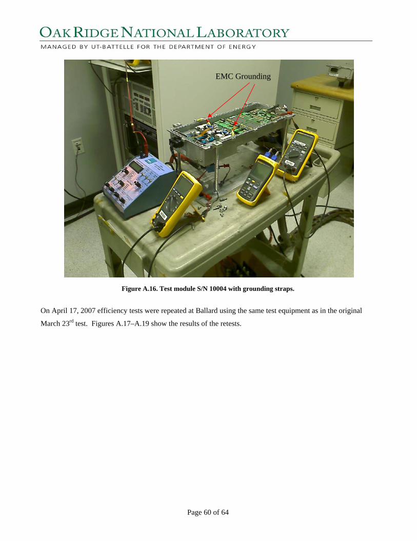
Page 60 of 64
Figure A.16. Test module S/N 10004 with grounding straps.
On April 17, 2007 efficiency tests were repeated at Ballard using the same test equipment as in the original
March 23rd test. Figures A.17–A.19 show the results of the retests.
EMC Grounding
Page 61 of 64
Tested Efficiency at 105 Deg C Coolant
60%
65%
70%
75%
80%
85%
90%
95%
0 1000 2000 3000 4000 5000 6000
Output Power (W)
Effic
ienc
y Vi=200V, Vo=13.3VVi=300V, Vo=13.3VVi=350V, Vo=13.3VVi=400V, Vo=13.3V
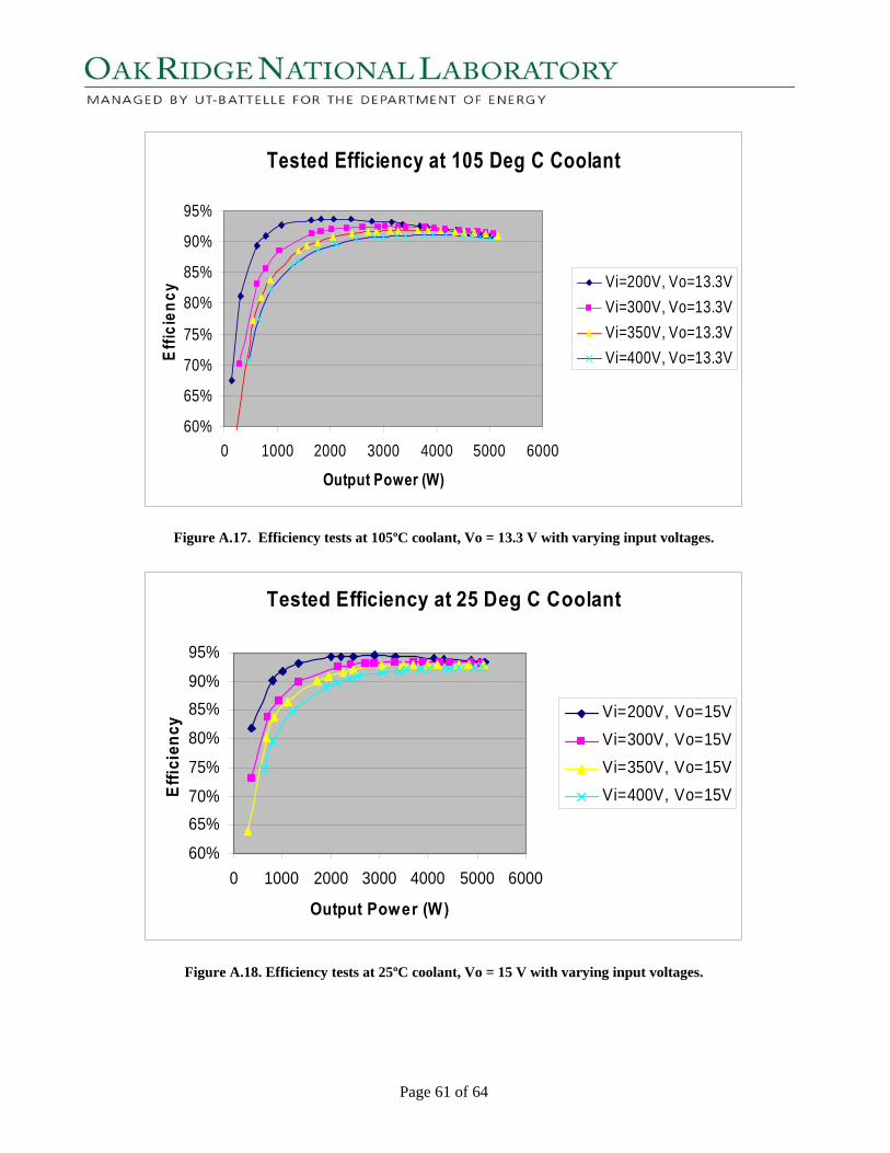
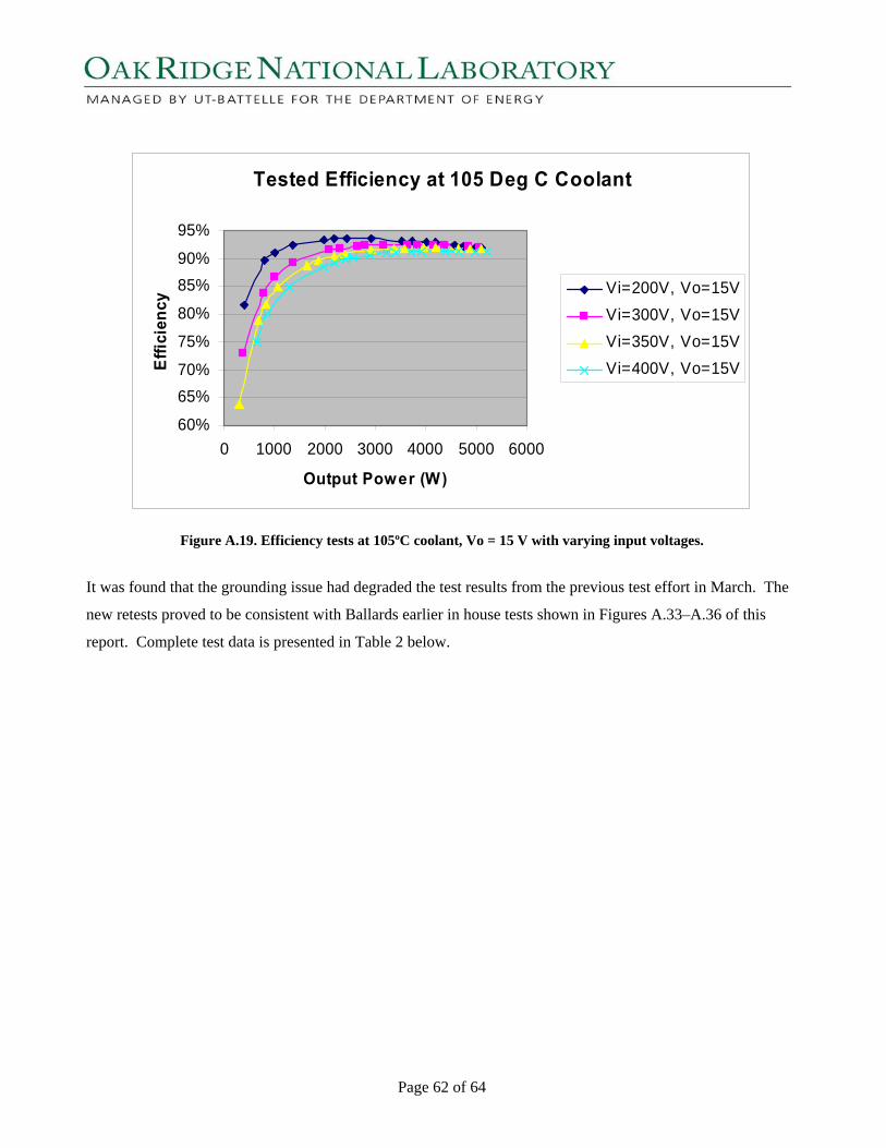
Figure A.17. Efficiency tests at 105ºC coolant, Vo = 13.3 V with varying input voltages.
Tested Efficiency at 25 Deg C Coolant
60%
65%70%
75%
80%
85%90%
95%
0 1000 2000 3000 4000 5000 6000
Output Power (W)
Effi
cien
cy
Vi=200V, Vo=15VVi=300V, Vo=15VVi=350V, Vo=15VVi=400V, Vo=15V
Figure A.18. Efficiency tests at 25ºC coolant, Vo = 15 V with varying input voltages.
Page 62 of 64
Tested Efficiency at 105 Deg C Coolant
60%
65%70%
75%
80%
85%90%
95%
0 1000 2000 3000 4000 5000 6000
Output Power (W)
Effic
ienc
y Vi=200V, Vo=15VVi=300V, Vo=15VVi=350V, Vo=15VVi=400V, Vo=15V
Figure A.19. Efficiency tests at 105ºC coolant, Vo = 15 V with varying input voltages. It was found that the grounding issue had degraded the test results from the previous test effort in March. The
new retests proved to be consistent with Ballards earlier in house tests shown in Figures A.33–A.36 of this
report. Complete test data is presented in Table 2 below.
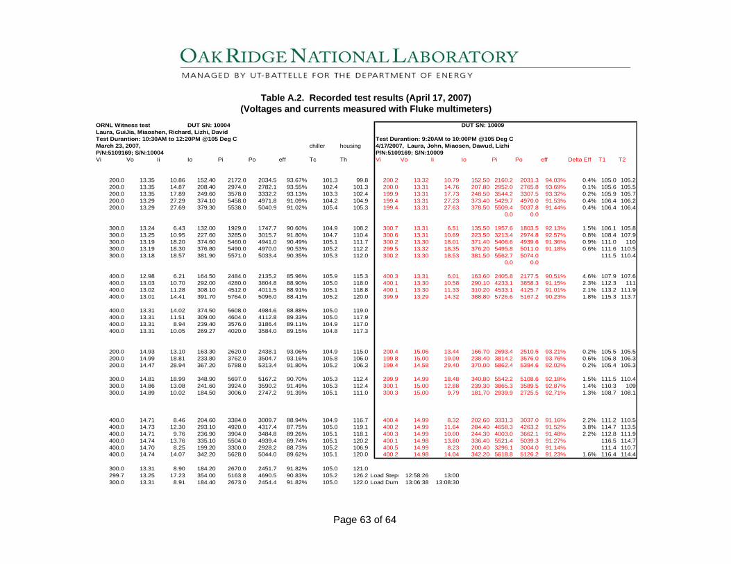
ORNL Witness test DUT SN: 10004 DUT SN: 10009Laura, GuiJia, Miaoshen, Richard, Lizhi, DavidTest Durantion: 10:30AM to 12:20PM @105 Deg C Test Durantion: 9:20AM to 10:00PM @105 Deg CMarch 23, 2007, chiller housing 4/17/2007, Laura, John, Miaosen, Dawud, LizhiP/N:5109169; S/N:10004 P/N:5109169; S/N:10009Vi Vo Ii Io Pi Po eff Tc Th Vi Vo Ii Io Pi Po eff Delta Eff T1 T2
200.0 13.35 10.86 152.40 2172.0 2034.5 93.67% 101.3 99.8 200.2 13.32 10.79 152.50 2160.2 2031.3 94.03% 0.4% 105.0 105.2200.0 13.35 14.87 208.40 2974.0 2782.1 93.55% 102.4 101.3 200.0 13.31 14.76 207.80 2952.0 2765.8 93.69% 0.1% 105.6 105.5200.0 13.35 17.89 249.60 3578.0 3332.2 93.13% 103.3 102.4 199.9 13.31 17.73 248.50 3544.2 3307.5 93.32% 0.2% 105.9 105.7200.0 13.29 27.29 374.10 5458.0 4971.8 91.09% 104.2 104.9 199.4 13.31 27.23 373.40 5429.7 4970.0 91.53% 0.4% 106.4 106.2200.0 13.29 27.69 379.30 5538.0 5040.9 91.02% 105.4 105.3 199.4 13.31 27.63 378.50 5509.4 5037.8 91.44% 0.4% 106.4 106.4
0.0 0.0
300.0 13.24 6.43 132.00 1929.0 1747.7 90.60% 104.9 108.2 300.7 13.31 6.51 135.50 1957.6 1803.5 92.13% 1.5% 106.1 105.8300.0 13.25 10.95 227.60 3285.0 3015.7 91.80% 104.7 110.4 300.6 13.31 10.69 223.50 3213.4 2974.8 92.57% 0.8% 108.4 107.9300.0 13.19 18.20 374.60 5460.0 4941.0 90.49% 105.1 111.7 300.2 13.30 18.01 371.40 5406.6 4939.6 91.36% 0.9% 111.0 110300.0 13.19 18.30 376.80 5490.0 4970.0 90.53% 105.2 112.2 299.5 13.32 18.35 376.20 5495.8 5011.0 91.18% 0.6% 111.6 110.5300.0 13.18 18.57 381.90 5571.0 5033.4 90.35% 105.3 112.0 300.2 13.30 18.53 381.50 5562.7 5074.0 111.5 110.4
0.0 0.0
400.0 12.98 6.21 164.50 2484.0 2135.2 85.96% 105.9 115.3 400.3 13.31 6.01 163.60 2405.8 2177.5 90.51% 4.6% 107.9 107.6400.0 13.03 10.70 292.00 4280.0 3804.8 88.90% 105.0 118.0 400.1 13.30 10.58 290.10 4233.1 3858.3 91.15% 2.3% 112.3 111400.0 13.02 11.28 308.10 4512.0 4011.5 88.91% 105.1 118.8 400.1 13.30 11.33 310.20 4533.1 4125.7 91.01% 2.1% 113.2 111.9400.0 13.01 14.41 391.70 5764.0 5096.0 88.41% 105.2 120.0 399.9 13.29 14.32 388.80 5726.6 5167.2 90.23% 1.8% 115.3 113.7
400.0 13.31 14.02 374.50 5608.0 4984.6 88.88% 105.0 119.0400.0 13.31 11.51 309.00 4604.0 4112.8 89.33% 105.0 117.9400.0 13.31 8.94 239.40 3576.0 3186.4 89.11% 104.9 117.0400.0 13.31 10.05 269.27 4020.0 3584.0 89.15% 104.8 117.3
200.0 14.93 13.10 163.30 2620.0 2438.1 93.06% 104.9 115.0 200.4 15.06 13.44 166.70 2693.4 2510.5 93.21% 0.2% 105.5 105.5200.0 14.99 18.81 233.80 3762.0 3504.7 93.16% 105.8 106.0 199.8 15.00 19.09 238.40 3814.2 3576.0 93.76% 0.6% 106.8 106.3200.0 14.47 28.94 367.20 5788.0 5313.4 91.80% 105.2 106.3 199.4 14.58 29.40 370.00 5862.4 5394.6 92.02% 0.2% 105.4 105.3
300.0 14.81 18.99 348.90 5697.0 5167.2 90.70% 105.3 112.4 299.9 14.99 18.48 340.80 5542.2 5108.6 92.18% 1.5% 111.5 110.4300.0 14.86 13.08 241.60 3924.0 3590.2 91.49% 105.3 112.4 300.1 15.00 12.88 239.30 3865.3 3589.5 92.87% 1.4% 110.3 109300.0 14.89 10.02 184.50 3006.0 2747.2 91.39% 105.1 111.0 300.3 15.00 9.79 181.70 2939.9 2725.5 92.71% 1.3% 108.7 108.1
400.0 14.71 8.46 204.60 3384.0 3009.7 88.94% 104.9 116.7 400.4 14.99 8.32 202.60 3331.3 3037.0 91.16% 2.2% 111.2 110.5400.0 14.73 12.30 293.10 4920.0 4317.4 87.75% 105.0 119.1 400.2 14.99 11.64 284.40 4658.3 4263.2 91.52% 3.8% 114.7 113.5400.0 14.71 9.76 236.90 3904.0 3484.8 89.26% 105.1 118.1 400.3 14.99 10.00 244.30 4003.0 3662.1 91.48% 2.2% 112.8 111.9400.0 14.74 13.76 335.10 5504.0 4939.4 89.74% 105.1 120.2 400.1 14.98 13.80 336.40 5521.4 5039.3 91.27% 116.5 114.7400.0 14.70 8.25 199.20 3300.0 2928.2 88.73% 105.2 106.9 400.5 14.99 8.23 200.40 3296.1 3004.0 91.14% 111.4 110.7400.0 14.74 14.07 342.20 5628.0 5044.0 89.62% 105.1 120.0 400.2 14.98 14.04 342.20 5618.8 5126.2 91.23% 1.6% 116.4 114.4
300.0 13.31 8.90 184.20 2670.0 2451.7 91.82% 105.0 121.0299.7 13.25 17.23 354.00 5163.8 4690.5 90.83% 105.2 126.2 Load Stepu 12:58:26 13:00300.0 13.31 8.91 184.40 2673.0 2454.4 91.82% 105.0 122.0 Load Dump 13:06:38 13:08:30
Table A.2. Recorded test results (April 17, 2007)(Voltages and currents measured with Fluke multimeters)
Page 63 of 64
Page 64 of 64
DISTRIBUTION Internal
1. D. J. Adams 2. K. P. Gambrell 3. E. C. Fox
4. L. D. Marlino 5. M. Olszewski 6. Laboratory Records
External
7. R. Al-Attar, DCX, [email protected]. 8. D. Blanck, Ballard Power Systems, 15001 Commerce Drive North, Dearborn, Michigan 48120. 9. T. Q. Duong, U.S. Department of Energy, EE-2G/Forrestal Building, 1000 Independence Avenue, S.W.,
Washington, D.C. 20585. 10. R. R. Fessler, BIZTEK Consulting, Inc., 820 Roslyn Place, Evanston, Illinois 60201-1724. 11. G. Hagey, Sentech, Inc., 501 Randolph St., Williamsburg, Virginia 23185. 12. E. Jih, Ford Motor Company, Scientific Research Laboratory, 2101 Village Road, MD-1170, Rm. 2331,
Dearborn, Michigan 48121. 13. K. J. Kelly, National Renewable Energy Laboratory, 1617 Cole Boulevard, Golden, Colorado 80401. 14. A. Lee, Daimler Chrysler, CIMS 484-08-06, 800 Chrysler Drive, Auburn Hills, Michigan 48326-2757. 15. F. Leonardi, Ford Motor Company, 15050 Commerce Drive, North, Dearborn, Michigan 48120-1261. 16. F. Liang, Ford Motor Company, Scientific Research Laboratory, 2101 Village Road, MD1170, Rm.
2331/SRL, Dearborn, Michigan 48121. 17. M. W. Lloyd, Energetics, Inc., 7164 Columbia Gateway Drive, Columbia, Maryland 21046. 18. J. Maquire, General Motors Advanced Technology Center, 3050 Lomita Boulevard, Torrance, California
90505. 19. M. Mehall, Ford Motor Company, Scientific Research Laboratory, 2101 Village Road, MD-2247, Rm.
3317, Dearborn, Michigan 48124-2053. 20. J. A. Montemarano, Naval Surfae Warfare Center, Carderock Division; Code 642, NSWD, 9500
MacArthur Boulevard; West Bethesday, Maryland 20817. 21. N. Olds, United States Council for Automotive Research (USCAR), [email protected] 22. S. A. Rogers, U.S. Department of Energy, EE-2G/Forrestal Building, 1000 Independence Avenue, S.W.,
Washington, D.C. 20585. 23. G. S. Smith, General Motors Advanced Technology Center, 3050 Lomita Boulevard, Torrance, California
90505. 24. E. J. Wall, U.S. Department of Energy, EE-2G/Forrestal Building, 1000 Independence Avenue, S.W.,
Washington, D.C. 20585. 25. B. Welchko, General Motors Advanced Technology Center, 3050 Lomita Boulevard, Torrance,
California 90505. 26. P. G. Yoshida, U.S. Department of Energy, EE-2G/Forrestal Building, 1000 Independence Avenue, S.W.,
Washington, D.C. 20585. 27. L. Zhu, Ballard Power Systems, 15001 Commerce Drive North, Dearborn, Michigan 48120.