David A. B. Miller Stanford University ...
26
Optical Interconnects Optical Interconnects Optical Interconnects Optical Interconnects David A. B. Miller David A. B. Miller Stanford University Stanford University http://ee.stanford.edu/~dabm http://ee.stanford.edu/~dabm 7/22/2008 7/22/2008 IAA Workshop, David A. B. Miller, Stanford IAA Workshop, David A. B. Miller, Stanford 1
Transcript of David A. B. Miller Stanford University ...

Optical InterconnectsOptical InterconnectsOptical InterconnectsOptical Interconnects
David A. B. MillerDavid A. B. MillerStanford UniversityStanford University
http://ee.stanford.edu/~dabmhttp://ee.stanford.edu/~dabm
7/22/20087/22/2008 IAA Workshop, David A. B. Miller, StanfordIAA Workshop, David A. B. Miller, Stanford 11

SummarySummary
Why optics for interconnectsWhy optics for interconnects•• DensityDensityDensityDensity•• EnergyEnergy
Challenges for optical technologyChallenges for optical technology
SiliconSilicon--compatible optical and optoelectronic technologycompatible optical and optoelectronic technology
Future possibilities with Future possibilities with nanophotonicsnanophotonics
7/22/20087/22/2008 IAA Workshop, David A. B. Miller, StanfordIAA Workshop, David A. B. Miller, Stanford 22

Levels of interconnectionLevels of interconnection
TelecommunicationsTelecommunications Campus networksCampus networks LANsLANs
10,000 km10,000 km 1000 km1000 km 1 km1 km 100 m100 m
interconnect distanceinterconnect distance
Optics currently dominates for long distance interconnectsOptics currently dominates for long distance interconnectsIncreasingly, optics is used in local area network applicationsIncreasingly, optics is used in local area network applications
7/22/20087/22/2008 IAA Workshop, David A. B. Miller, StanfordIAA Workshop, David A. B. Miller, Stanford 33

Levels of interconnectionLevels of interconnection
Backplanes & boardBackplanes & board--toto--boardboard ChipChip--toto--chipchip OnOn--chipchip
1 m1 m 10 cm10 cm 1 mm1 mm
interconnect distanceinterconnect distance
Electrical signaling within computers is encountering severe limitations Electrical signaling within computers is encountering severe limitations ---- can optics help can optics help at these length scales?at these length scales?
7/22/20087/22/2008 IAA Workshop, David A. B. Miller, StanfordIAA Workshop, David A. B. Miller, Stanford 44

The Interconnect ProblemThe Interconnect Problem
There are many more short connections than long onesThere are many more short connections than long ones•• With vastly greater amounts of information communicated at short distancesWith vastly greater amounts of information communicated at short distances
–– E.g., Tb/s across a chipE.g., Tb/s across a chip•• These interconnects are known to be a major problemThese interconnects are known to be a major problem
“For the long term, material innovation with traditional scaling will no longer satisfy performance “For the long term, material innovation with traditional scaling will no longer satisfy performance requirements. Interconnect innovation with optical, RF, or vertical integration … will deliver therequirements. Interconnect innovation with optical, RF, or vertical integration … will deliver therequirements. Interconnect innovation with optical, RF, or vertical integration … will deliver the requirements. Interconnect innovation with optical, RF, or vertical integration … will deliver the solution” (International Technology Roadmap for Semiconductors 2003)solution” (International Technology Roadmap for Semiconductors 2003)
7/22/20087/22/2008 IAA Workshop, David A. B. Miller, StanfordIAA Workshop, David A. B. Miller, Stanford 55Source: IntelSource: Intel

Wiring, Optics, and Communicating Information Wiring, Optics, and Communicating Information --Architectural “Aspect Ratio” Limit to CapacityArchitectural “Aspect Ratio” Limit to Capacity
AA
Get universal form of scaling for simple digital connections (no
this wirethis wirecarries the same carries the same
number of bits per number of bits per second assecond as
this wirethis wire Miller and Ozaktas (1997)Miller and Ozaktas (1997)
Get universal form of scaling for simple digital connections (no repeaters, no multilevel modem techniques)
bit rate Bbit rate B ∝∝ A / A / 22Once the wiring fills all space, Once the wiring fills all space,
the capacity cannot bethe capacity cannot beB ~ 10B ~ 101515 A / A / 22 bits/s for LC linesbits/s for LC lines
B ~ 10B ~ 101616 A / A / 22 bits/s for RC linesbits/s for RC lines
the capacity cannot be the capacity cannot be increased either by making the increased either by making the system smaller or making it system smaller or making it largerlarger
Optics completely avoids this Optics completely avoids this scaling limitationscaling limitation
7/22/2008 IAA Workshop, David A. B. Miller, Stanford 6
B ~ 10B ~ 101717 A / A / 22 bits/s for equalized LC linesbits/s for equalized LC linessca g tat osca g tat o
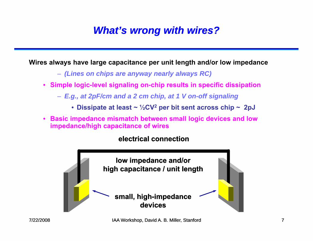
What’s wrong with wires?What’s wrong with wires?
Wires always have large capacitance per unit length and/or low impedance– (Lines on chips are anyway nearly always RC)(Lines on chips are anyway nearly always RC)
• Simple logic-level signaling on-chip results in specific dissipation– E.g., at 2pF/cm and a 2 cm chip, at 1 V on-off signaling
Di i t t l t ½CV2 bit t hi 2 J• Dissipate at least ~ ½CV2 per bit sent across chip ~ 2pJ• Basic impedance mismatch between small logic devices and low
impedance/high capacitance of wires
electrical connectionelectrical connection
low impedance and/orlow impedance and/or//
small highsmall high impedanceimpedance
high capacitance / unit lengthhigh capacitance / unit length
7/22/20087/22/2008 IAA Workshop, David A. B. Miller, StanfordIAA Workshop, David A. B. Miller, Stanford 77
small, highsmall, high--impedanceimpedancedevicesdevices

Optical and Electronic PhysicsOptical and Electronic Physics-- DifferencesDifferences
Very short wavelengthVery short wavelength500 nm500 nm
(electronics 3 cm (electronics 3 cm -- 30 m)30 m)(( ))
OpticsOptics
Very high frequencyVery high frequency500 THz500 THz
(electronics 10 MHz(electronics 10 MHz -- 10 GHz)10 GHz)
Large photon energyLarge photon energy2 eV2 eV
(electronics 40 neV(electronics 40 neV -- 40 µeV)40 µeV)(electronics 10 MHz (electronics 10 MHz 10 GHz)10 GHz) (electronics 40 neV (electronics 40 neV 40 µeV)40 µeV)
7/22/20087/22/2008 IAA Workshop, David A. B. Miller, StanfordIAA Workshop, David A. B. Miller, Stanford 88
Miller 1997Miller 1997
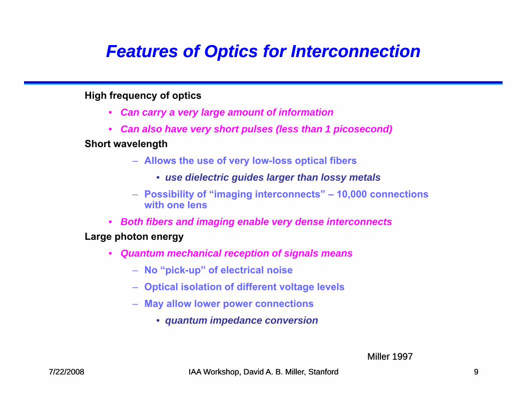
Features of Optics for InterconnectionFeatures of Optics for Interconnection
High frequency of optics• Can carry a very large amount of information
C l h h t l (l th 1 i d)• Can also have very short pulses (less than 1 picosecond)Short wavelength
– Allows the use of very low-loss optical fibers• use dielectric guides larger than lossy metals• use dielectric guides larger than lossy metals
– Possibility of “imaging interconnects” – 10,000 connections with one lens
• Both fibers and imaging enable very dense interconnectsLarge photon energy
• Quantum mechanical reception of signals means– No “pick-up” of electrical noise– Optical isolation of different voltage levels– May allow lower power connections
• quantum impedance conversion
7/22/20087/22/2008 IAA Workshop, David A. B. Miller, StanfordIAA Workshop, David A. B. Miller, Stanford 99
Miller 1997Miller 1997

Quantum Impedance ConversionQuantum Impedance Conversion
modulatormodulator detectordetectormodulatormodulator detectordetector
optical connectionoptical connection
modulator and detector eachmodulator and detector eachhave one electron per photonhave one electron per photon
hence currenthence current--toto--power impedance transformationpower impedance transformationhence optical devices can impedancehence optical devices can impedance--match match
7/22/20087/22/2008 IAA Workshop, David A. B. Miller, StanfordIAA Workshop, David A. B. Miller, Stanford 1010
p pp psmall electronic devicessmall electronic devices Miller 1989Miller 1989

Example Calculation of Quantum Example Calculation of Quantum Impedance ConversionImpedance Conversion
Suppose 1 nW optical beampp p• classical voltage (e.g., from side to side of linearly
polarized light beam– 600 microvolts in 377 ohm impedance
Presume 1 eV photonsPresume simple photodiode operating with a 1 gigaohm load
• Then 1 nW of light can generate about 1 nA of current• Then 1 nW of light can generate about 1 nA of current, – 1 V in 1 gigaohm load
• photodiode has performed “quantum impedance transformation”transformation
7/22/20087/22/2008 IAA Workshop, David A. B. Miller, StanfordIAA Workshop, David A. B. Miller, Stanford 1111
Miller 1989Miller 1989

Key physical benefits of optics for Key physical benefits of optics for interconnectsinterconnects
Bandwidth Bandwidth •• density off the edgedensity off the edge –– connector densityconnector densitydensity off the edge density off the edge connector densityconnector density•• density over distance density over distance –– long wiring densitylong wiring density
–– Breaks the link between crossBreaks the link between cross--sectional area and the sectional area and the combination of distance and bandwidthcombination of distance and bandwidthcombination of distance and bandwidthcombination of distance and bandwidth
EnergyEnergy•• don’t need to charge the whole “wire”don’t need to charge the whole “wire”
d ’t d t h “ i ” t l i l i l ltd ’t d t h “ i ” t l i l i l lt•• don’t need to charge “wires” to classical signal voltagesdon’t need to charge “wires” to classical signal voltages–– avoid bit flips by physically reavoid bit flips by physically re--routing signals without routing signals without
reading all the bits?reading all the bits?
7/22/20087/22/2008 IAA Workshop, David A. B. Miller, StanfordIAA Workshop, David A. B. Miller, Stanford 1212

Wiring, Optics, and Communicating Information Wiring, Optics, and Communicating Information ––Optics as a Solution at Many Levels?Optics as a Solution at Many Levels?
Optics as a solution at many levels?• E.g., all the way to the chip?
Requirements on optical technology• integration for performance, cost
– For shorter distances, low power more important• integration and efficient devices essential
– Electrical system energies• ~ 1pJ per bit (≡ 1 mW/(Gb/s)) for global interconnections on p p ( ( )) g
chip• ~ 10 pJ per bit for on-module (chip – chip) interconnections
(future chips may need 10 – 100 Tb/s of I/O bandwidth)• ~ 100 pJ per bit for backplane connections?
• Optical output device energies would need to be – x10 lower than these system energies so as not to increase
7/22/20087/22/2008 IAA Workshop, David A. B. Miller, StanfordIAA Workshop, David A. B. Miller, Stanford 1313
energy compared to electrical, – and should be x100 lower to give enough incentive
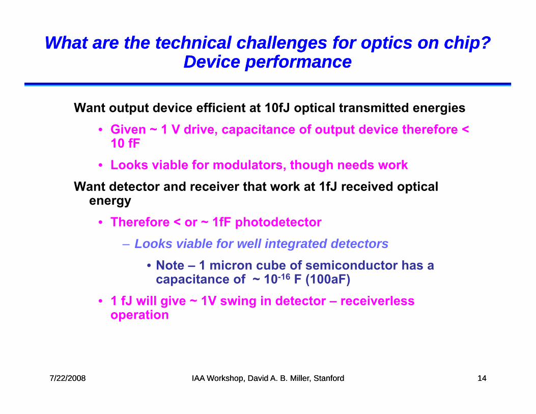
What are the technical challenges for optics on chip?What are the technical challenges for optics on chip?Device performanceDevice performance
Want output device efficient at 10fJ optical transmitted energies• Given ~ 1 V drive capacitance of output device therefore <• Given ~ 1 V drive, capacitance of output device therefore <
10 fF• Looks viable for modulators, though needs work
Want detector and receiver that work at 1fJ received optical energy
• Therefore < or ~ 1fF photodetector– Looks viable for well integrated detectors
• Note – 1 micron cube of semiconductor has a capacitance of ~ 10-16 F (100aF)p ( )
• 1 fJ will give ~ 1V swing in detector – receiverlessoperation
7/22/20087/22/2008 IAA Workshop, David A. B. Miller, StanfordIAA Workshop, David A. B. Miller, Stanford 1414

What are the technical challenges for optics What are the technical challenges for optics to the to the chip? chip? Systems Systems and integration requirementsand integration requirements
Need to work at CMOS voltages < or ~ 1VNeed to work at very high speedsy g p
• Need technology with >> 10GHz speed possibilities
N d d ti l h lNeed dense optical channels– At least as dense as current off-chip wiring
channels• Otherwise cannot make a significant impact on
the global interconnect trafficH d 1000’ f h l– Hence need ~ 1000’s of channels
• Need to consider wavelength division multiplexing (WDM)
7/22/20087/22/2008 IAA Workshop, David A. B. Miller, StanfordIAA Workshop, David A. B. Miller, Stanford 1515
Must be manufacturable in integrated platform with CMOS
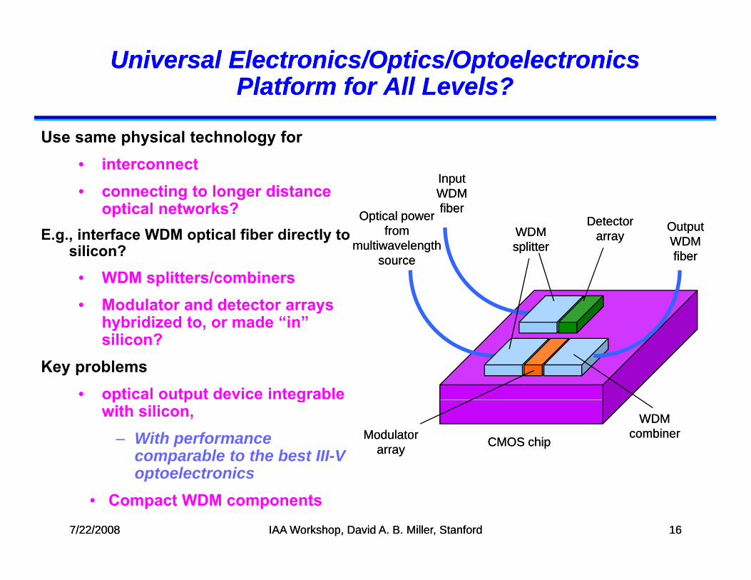
Universal Electronics/Optics/Optoelectronics Universal Electronics/Optics/Optoelectronics Platform for All Levels?Platform for All Levels?
Use same physical technology for • interconnect
InputInput• connecting to longer distance
optical networks?E.g., interface WDM optical fiber directly to
silicon?Output Output WDM WDM fibfib
Input Input WDM WDM fiberfiberOptical power Optical power
from from multiwavelength multiwavelength
WDM WDM splittersplitter
Detector Detector arrayarray
silicon?
• WDM splitters/combiners• Modulator and detector arrays
hybridized to, or made “in”
fiberfibersourcesource
hybridized to, or made in silicon?
Key problems • optical output device integrablep p g
with silicon, – With performance
comparable to the best III-V optoelectronics
CMOS chipCMOS chip
WDM WDM combinercombinerModulator Modulator
arrayarray
7/22/20087/22/2008 IAA Workshop, David A. B. Miller, StanfordIAA Workshop, David A. B. Miller, Stanford 1616
optoelectronics• Compact WDM components

Silicon Photonics TechnologySilicon Photonics Technology
Silicon photonics technology• Impressive developments in photonics compatible withImpressive developments in photonics compatible with
silicon manufacturebroad range of demonstrated optical waveguide, detector, and
modulator technologies with • silicon, silicon dioxide, silicon nitride, SiGe and Ge
– all of these materials can be grown compatible with silicon CMOS fabrication technology
7/22/20087/22/2008 IAA Workshop, David A. B. Miller, StanfordIAA Workshop, David A. B. Miller, Stanford 1717

Silicon Photonics DevicesSilicon Photonics Devices
waveguides• e.g., silicon ridge on SiO2 (SOI),
ili “ i ”silicon “wire”detectors
• Ge detectors on siliconH t l (2006)
10um fiber core10um fiber core
– e.g., Huang et al. (2006), Koester et al. (2006), Colace et al. (2006), Luxtera Corp.
– Ge detectors integrated with ili t i t (Ok t l
waveguideswaveguidessilicon transistors (Okyay et al. 2007)
gg
Luxtera Corp. (courtesy Cary Gunn)Luxtera Corp. (courtesy Cary Gunn)
7/22/20087/22/2008 IAA Workshop, David A. B. Miller, StanfordIAA Workshop, David A. B. Miller, Stanford 1818

Silicon Photonics DevicesSilicon Photonics Devices
modulators• refractive modulators based on carrier density
index changeindex change• technically very impressive use of a very weak
mechanism– Mach-Zehnder modulators
• see, e.g., Liao et al. (2006), Green et al. (2007), Luxtera Corp.
– But high operating energies (~ 10 pJ pJ per bit)pJ pJ per bit)
– ring-resonator modulators• see, e.g., review by Lipson (2006),
Luxtera Corp.– though high-Q devices needing
very precise tuning– Ge and Ge quantum well
electroabsorption modulatorscourtesy Michal Lipson (Cornell)courtesy Michal Lipson (Cornell)
7/22/20087/22/2008 IAA Workshop, David A. B. Miller, StanfordIAA Workshop, David A. B. Miller, Stanford 1919
electroabsorption modulators

Strained Strained GeGe//SiGeSiGe Multiple Quantum WellsMultiple Quantum Wells
10nm Ge well 10nm Ge well 16nm SiGe barrier16nm SiGe barrier16nm SiGe barrier16nm SiGe barrier
Regular and sharp MQW Regular and sharp MQW structure structure grown on silicon substratesgrown on silicon substrates
Quantum wells offer the most effectiveQuantum wells offer the most effective
7/22/20087/22/2008 IAA Workshop, David A. B. Miller, StanfordIAA Workshop, David A. B. Miller, Stanford 2020
Quantum wells offer the most effective Quantum wells offer the most effective optical modulation mechanismoptical modulation mechanism Y. H. KuoY. H. Kuo
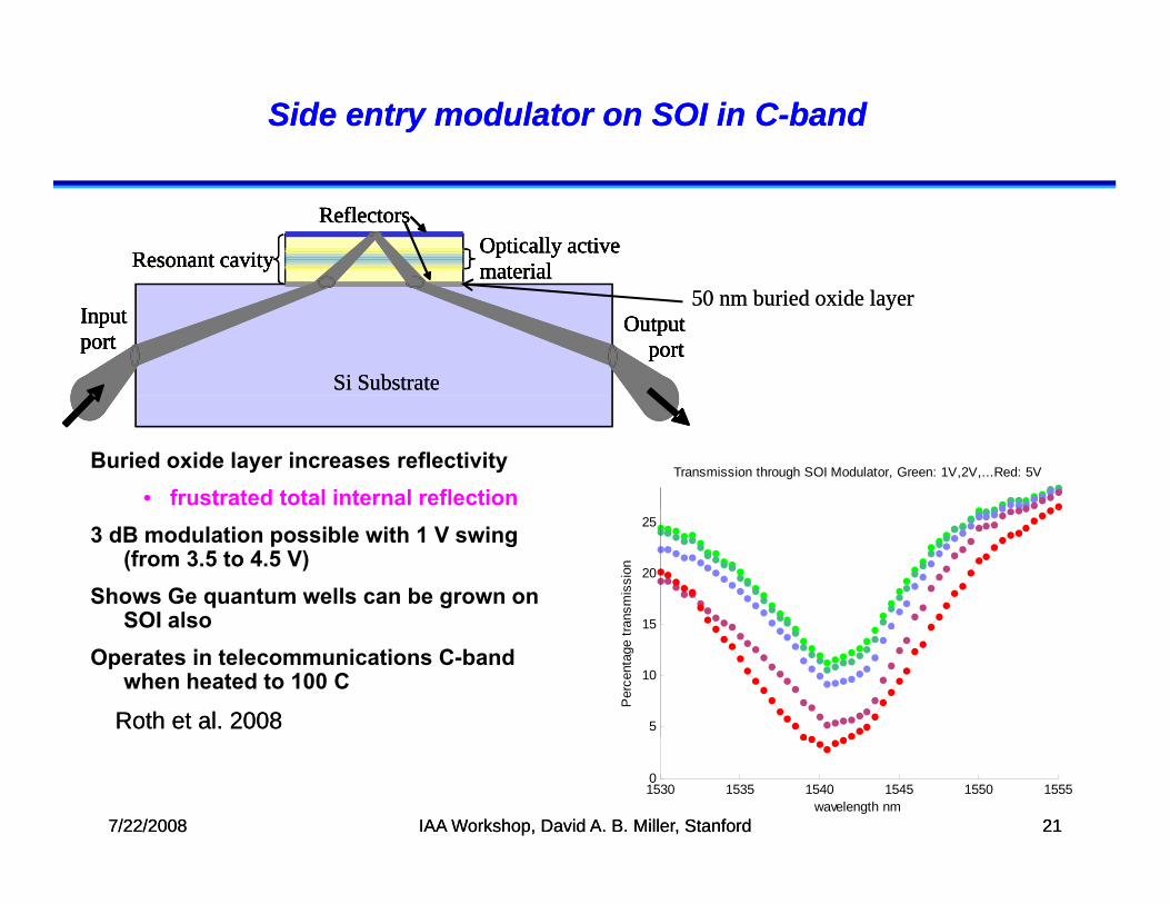
Side entry modulator on SOI in CSide entry modulator on SOI in C--bandband
ReflectorsReflectorsOptically active Optically active materialmaterialResonant cavityResonant cavity
ReflectorsReflectorsOptically active Optically active materialmaterialResonant cavityResonant cavity
SubstrateSubstrate
Input Input portport
Output Output portport
Si SubstrateSi Substrate
Input Input portport
Output Output portport
50 nm buried oxide layer 50 nm buried oxide layer
Buried oxide layer increases reflectivity • frustrated total internal reflection
Transmission through SOI Modulator, Green: 1V,2V,...Red: 5V
3 dB modulation possible with 1 V swing (from 3.5 to 4.5 V)
Shows Ge quantum wells can be grown on SOI also 15
20
25
ansm
issi
onSOI also
Operates in telecommunications C-band when heated to 100 C
5
10
15P
erce
ntag
e tra
Roth et al. 2008Roth et al. 2008
7/22/20087/22/2008 IAA Workshop, David A. B. Miller, StanfordIAA Workshop, David A. B. Miller, Stanford 2121
1530 1535 1540 1545 1550 15550
wavelength nm

Dipole Antenna Enhanced Dipole Antenna Enhanced PhotodetectorPhotodetector for for 1.3 micron Wavelength1.3 micron Wavelength
AntennaAntennaGoal Goal –– couple into deeply subwavelength couple into deeply subwavelength
detectorsdetectorsAntenna Antenna armsarms Ge Ge
detector detector elementelement
•• ultraultra--low capacitance (<< 1 fF)?low capacitance (<< 1 fF)?•• high speed (~ 1 ps)?high speed (~ 1 ps)?
Concept Concept –– Hertz dipole antennaHertz dipole antenna
XX
YY
pp pp•• 160 nm long dipole antenna arms160 nm long dipole antenna arms•• current collecting “sleeve” armscurrent collecting “sleeve” arms
surprisingly little effect onsurprisingly little effect onXX
Collecting Collecting electrodeselectrodes
–– surprisingly little effect on surprisingly little effect on antenna behaviorantenna behavior
Ge detector element: Ge detector element: •• 150nm long (between collection150nm long (between collection
500 nm500 nm•• 150nm long (between collection 150nm long (between collection
electrode), 50nm wide (between electrode), 50nm wide (between antenna arms) and 80nm thickantenna arms) and 80nm thick
•• “plane“plane--parallel” capacitance ~ 5 aFparallel” capacitance ~ 5 aF
7/22/20087/22/2008 IAA Workshop, David A. B. Miller, StanfordIAA Workshop, David A. B. Miller, Stanford 2222
Tang et al. Tang et al. 20082008

Mask and layout for Mask and layout for nanoantennananoantenna
7/22/20087/22/2008 IAA Workshop, David A. B. Miller, StanfordIAA Workshop, David A. B. Miller, Stanford 2323

CMOS Detector with Nanometallic Enhancement CMOS Detector with Nanometallic Enhancement –– Hole Cut for Nanometallic FabricationHole Cut for Nanometallic Fabrication
nn
p
40nm
p
40nm40nm
Fabricated CFabricated C--aperture in Al layer on silicon for nanometallicaperture in Al layer on silicon for nanometallicFabricated CFabricated C--aperture in Al layer on silicon for nanometallic aperture in Al layer on silicon for nanometallic enhanced enhanced photodetectionphotodetection
•• 3 times greater photocurrent per unit detector area than 3 times greater photocurrent per unit detector area than large area detector without nanometallic enhancementlarge area detector without nanometallic enhancement
Tang et al. Tang et al. 20082008First nanometallic device integrated with commercial CMOSFirst nanometallic device integrated with commercial CMOS
7/22/20087/22/2008 2424IAA Workshop, David A. B. Miller, StanfordIAA Workshop, David A. B. Miller, Stanford

Compact WDM splitters? Compact WDM splitters? Nanophotonic Nanophotonic superprismsuperprism array wavelength splitterarray wavelength splitter
Could we make very compact wavelength spliters?
In Focussing lenswavelength spliters?
“Superprism” effects in photonic nanostructures
l ti f z
x
• very large separation of wavelengths in compact structure
• form of dispersion can be
zy
Mirror
Mirror
Substrate• form of dispersion can be engineered by design
• e.g., 66 layer non-periodic structure separates 4
DielectricStack
Out 1structure separates 4 wavelengths
• Many possibilities also with photonic-crystal-like structures
Out 1Out 2Out 3Out 4
7/22/20087/22/2008 IAA Workshop, David A. B. Miller, StanfordIAA Workshop, David A. B. Miller, Stanford 2525
p y
Nelson et al. 2000Nelson et al. 2000
ConclusionsConclusions
Optics has many attractive features for interconnects• especially energy and density
Silicon photonics has been advancing rapidlyGe quantum wells on silicon may give “missing” output device
• mechanism in Group IV semiconductors as good as the best in III-V’sp g• 2 – 3 orders of magnitude stronger mechanism than carrier density index
change in silicon Very promising for devices
• Integrated with CMOS• With high speed and low power• Possible basis for one technology platform from interconnects to long haul• Possible basis for one technology platform from interconnects to long haul
Nanometallics offer new possibilities for sub-wavelength optoelectronicsNew nanophotonic options available for wavelength splitting
7/22/20087/22/2008 IAA Workshop, David A. B. Miller, StanfordIAA Workshop, David A. B. Miller, Stanford 2626