Datasheet - Panasonic · Datasheet Ver. BEF Page 1 of 14 Established: 2012-11-21 Revised:...
15
Datasheet Ver. BEF Page 1 of 14 Established: 2012-11-21 Revised: 2013-05-30 Applications ■ WCDMA handset ■ HSDPA ■ HSUPA ■ LTE Type ■ Hybrid Integrated Circuit Features ■ High efficiency operation 47% @ 28.5dBm ■ Small, low profile LGA package 3mm x 3mm x 0.85mm (1mm Max) ■ Low Voltage Positive Bias Supply (3.2V to 4.35V) ■ 2-Mode Power States with Digital Control Interface ■ Optimized for DC/DC converter operation ■ Integrated Power Coupler ■ Integrated Blocking capacitors UMTS Band 11/21 Power Amplifier IC (1427.9MHz to 1462.9MHz) UN06B11 Vcc1 RF in Vmode NC Ven Vcc2 RF out CP in GND CP out 1 5 4 3 2 6 7 8 9 Bias Circuit 10
Transcript of Datasheet - Panasonic · Datasheet Ver. BEF Page 1 of 14 Established: 2012-11-21 Revised:...

Datasheet
Ver. BEF Page 1 of 14 Established: 2012-11-21 Revised: 2013-05-30
Applications WCDMA handset HSDPA HSUPA LTE
Type Hybrid Integrated Circuit
Features High efficiency operation 47% @ 28.5dBm Small, low profile LGA package 3mm x 3mm x 0.85mm (1mm Max) Low Voltage Positive Bias Supply (3.2V to 4.35V) 2-Mode Power States with Digital Control Interface Optimized for DC/DC converter operation Integrated Power Coupler Integrated Blocking capacitors
UMTS Band 11/21 Power Amplifier IC(1427.9MHz to 1462.9MHz)
UN06B11
Vcc1
RF in
Vmode
NC
Ven
Vcc2
RF out
CP in
GND
CP out
1
5
4
3
2
6
7
8
9
BiasCircuit
10
Datasheet
Ver. BEF Page 2 of 14 Established: 2012-11-21 Revised: 2013-05-30
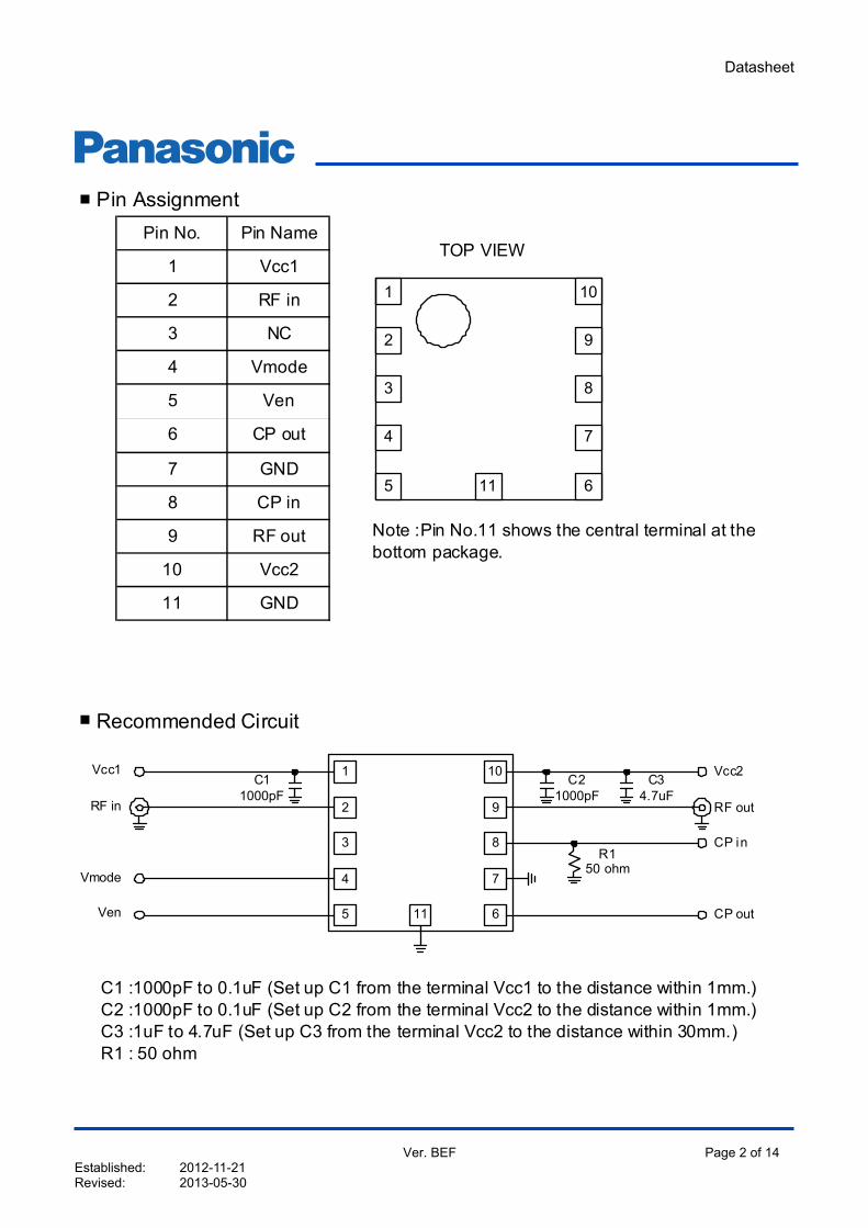
Pin AssignmentPin No. Pin Name
TOP VIEW1 Vcc1
2 RF in
3 NC
4 Vmode
5 Ven
6 CP out
7 GND
8 CP in
9 RF out
10 Vcc2
11 GND
Recommended Circuit
C1 :1000pF to 0.1uF (Set up C1 from the terminal Vcc1 to the distance within 1mm.)C2 :1000pF to 0.1uF (Set up C2 from the terminal Vcc2 to the distance within 1mm.)C3 :1uF to 4.7uF (Set up C3 from the terminal Vcc2 to the distance within 30mm.)R1 : 50 ohm
Note :Pin No.11 shows the central terminal at thebottom package.
1
2
3
4
5
10
9
8
7
611
3
4
5
10
9
8
7
6
1
2
Vcc1
RF in
Vmode
Ven
Vcc2
RF out
CP in
CP out
C11000pF
C34.7uF
C21000pF
R150 ohm
11

Datasheet
Ver. BEF Page 3 of 14 Established: 2012-11-21 Revised: 2013-05-30
High-power mode(HPM) High
Shut down mode -Low Low
Low-power mode(LPM) High High ≤
HSPA LTEPmax
Low ≤ 27.25 27.2528.5
Parameter Ven Vmode Rel99
85 Ambient Temperature UMTS / LTE -30Ta
0.5V
1.8 3.1Mode Control Voltage
Low 0
High 1.35Vmode
0.5V
1.8 3.1
V
Enable VoltageLow 0
High 1.35Ven
Vcc1
Supply Voltage 2 0.4Vcc2 3.4 4.35
-35 to +150
Supply Voltage 1 3.2 3.4 4.35 V
Operating Frequency
Storage temperature Tstg
1427.9
Typ
f
1462.9 MHz
1
UnitParameter Symbol
NotesParameter Condit ion Symbol Min Max Unit
V4.2
NotesRating
Supply voltage Vcc1,2 6 V
14
Operating Ranges
Modes of operation
dBm
1,2
1,3
1Control voltage Ven,Vmode
Input RF power Pin
-
≤
15
-
≤ 14
≤
≤
10
Absolute Maximum Ratings
Datasheet
Ver. BEF Page 4 of 14 Established: 2012-11-21 Revised: 2013-05-30
Vcc1=3.4V, Ven=1.8V, Ta=+25, ZS=ZL=50Ωf=1427.9 to 1462.9MHz Signal Condition:Rel99 Pmax: refer to Page.4.
Vcc1=3.4V, Ven=1.8V, Ta=+25, ZS=ZL=50Ωf=1427.9 to 1462.9MHz Signal Condition:HSPA
47Power Added Efficiency PAE
HPM, Pout=28.5dBm,Vcc2=3.4V 41LPM, Pout=15dBm,Vcc2=1.1V 22
dBc
µA
mA
Parameter Min Typ Max
105
Unit
-42
26.5
Electrical performance-1
Symbol Condition
5MHz offset
ACLR1 HPM, Pout=28.5dBm,Vcc2=3.4V
Vcc=3.4V, Pin=off,Ven=0V
mA
4
%
25
-42
446
-57
5
-36
27
Input impedance VSWR
Ioff
dBc
dBc
ρIN
Ien
3f0
1.5:1
30
2nd harmonic
Leakage Current
Quiescent current
Enable current
3rd harmonic and higher
0.1
-47
Adjacent channelleakage power ratio1
Adjacent channelleakage power ratio2
2f0
LPM, Pout=15dBm,Vcc2=1.1VLPM_Pout=-30dBm,Vcc2=0.4V
Mode control current
Iidle
Imode
LPM_Pout=-30dBm,Vcc2=0.4V
HPM, Pout=Pmax
40125
HPM, Pout=28.5dBm,Vcc2=3.4V
16.512.0LPM, Pout=15dBm,Vcc2=1.1V
510
10MHz offset
Notes
dB28.5
Gain
HPM, Pout=28.5dBm,Vcc2=3.4V
LPM_Pout=-30dBm,Vcc2=0.4VTotal Supply Current LPM, Pout=15dBm,Vcc2=1.1VIct
GHPM, Pout=28.5dBm,Vcc2=3.4V
10
0.1
dBc
Max
mA
2.5:1
-35
-46
Notes
ACLR2
Vcc2=0.5V, Pin=off,Ven=1.8V
Symbol
-46
HPM, Pout=Pmax
HPM, Pout=Pmax
4
mA
Electrical performance-2
Adjacent channelleakage power ratio4 ACLR4
ACLR3Adjacent channelleakage power ratio3
HPM:Vcc2=3.4V,LPM:Vcc2=1.12V
10MHz offsetPout = Pmax-MPR
HPM:Vcc2=3.4V,LPM:Vcc2=1.12V4-36
dBc
Unit
5MHz offset
-40 dBc
Typ
Pout = Pmax-MPR -42
-58
Condition Min
Vmode=1.8V
LPM, Pout=15dBm,Vcc2=1.1V
Parameter
4

Datasheet
Ver. BEF Page 5 of 14 Established: 2012-11-21 Revised: 2013-05-30
Vcc1=Vcc2=3.4V, Ven=1.8V, Ta=+25, ZS=ZL=50Ωf=1427.9 to 1462.9MHz Signal Condition:LTE
Vcc1=Vcc2=3.4V, Ven=1.8V, Ta=+25, ZS=ZL=50Ωf=1427.9 to 1462.9MHz
Vcc1=Vcc2=3.4V, Ven=1.8V, Ta=+25, ZS=ZL=50Ωf=1427.9 to 1462.9MHz
f=1427.9 to 1462.9MHz
VSWR ≤ 5:1, all phase
ISM noise NP3 Pout ≤ Pmax
GPS noise NP2 Pout ≤ Pmax1574 to 1577 MHz
CF
dBm/Hz
Notes
Min
Pout ≤ Pmax
NP1
ACLR5
UTRA_ACLR2
Condition
4,5-33 dBcHPM:Vcc2=3.4V,LPM:Vcc2=1.12V
all phase
dBm/Hz
dBc-36
-133
UnitMax
dBm/Hz
4,5
4,5
Max
-70
Unit Notes
-135
-134
Notes
dBc
E-UTRA_ACLRAdjacent channelleakage power ratio5
Condition
-41
Parameter Symbol Min Typ
ACLR6
Typ
-39
-39
698 to 2620 MHz,
Typ
-135Pout ≤ Pmax
-1422400 to 2483.5 MHz
0.25
Coupler factor 20
CPL_IN to CPL_OUT ports,
19
Daisy-chain insertion lossEnable = low
DCil 0.1
8:1
Condition
Pout ≤ Pmax
dBc
-137
Symbol
S
Electrical performance-5
Symbol Condition Min Typ UnitMax
48 MHz offset from Tx
dB
Electrical performance-4
dB21
RX noise
Parameter
-47ACLR7
UTRA_ACLR1
HPM:Vcc2=3.4V,LPM:Vcc2=1.12V
Max UnitSymbol NotesMin
Pout = Pmax-MPR
Electrical performance-6
stabil ity, spurious levels
Ruggedness R
Parameter
Pout = Pmax-MPRAdjacent channelleakage power ratio6
Adjacent channelleakage power ratio7
Electrical performance-3
Parameter
HPM:Vcc2=3.4V,LPM:Vcc2=1.12V
Pout = Pmax-MPR

Datasheet
Ver. BEF Page 6 of 14 Established: 2012-11-21 Revised: 2013-05-30
Vcc1=3.4V, Ven=1.8V, Ta=-30 to +85 , ZS=ZL=50Ωf=1427.9 to 1462.9MHz
Vcc1=Vcc2=3.4V, Ven=1.8V, Ta=-30 to +85 , ZS=ZL=50Ωf=1427.9 to 1462.9MHz
Vcc=3.4V, Ven=1.8V, Ta=+25, ZS=ZL=50Ωf=1427.9 to 1462.9MHz
Notes
Signal Condition:LTE
Signal Condition:Rel99, HSPAParameter
4,5
Typ Unit
Typ
Min Notes
Notes
Signal Condition:Rel99
dBc
-31 dBc
-46
NotesUnit
Max
-34 dBc
Max
dBc 4-34
Part to part variation -10 10 deg
Min Max
Unit
E-UTRA_ACLR
HPM:Vcc2=3.4V,LPM:Vcc2=1.12V
Symbol Condition Typ
Electrical performance-7
ConditionParameter Symbol
Phase discontinuity variation Pdv
UTRA_ACLR2ACLR12 HPM:Vcc2=3.4V,LPM:Vcc2=1.12V
Adjacent channelleakage power ratio10
Adjacent channelleakage power ratio11
UTRA_ACLR1
HPM:Vcc2=3.4V,LPM:Vcc2=1.12VPout = Pmax-MPR-0.3dBACLR
11
ACLR10 Pout = Pmax-MPR-0.3dB
4,5
-37 dBc 4,5Pout = Pmax-MPR-0.3dBAdjacent channelleakage power ratio12
Parameter Symbol Condition Min
5MHz offsetPout = Pmax-MPR-0.3dBHPM:Vcc2=3.4V,LPM:Vcc2=1.1V
Adjacent channelleakage power ratio9 ACLR9
10MHz offset
Adjacent channelleakage power ratio8
Electrical performance-8
Electrical performance-9
4Pout = Pmax-MPR-0.3dBHPM:Vcc2=3.4V,LPM:Vcc2=1.1V
ACLR8
1: The backside ground of the package should be soldered to cellular phone P.C.B.2: Ven=0V3: Vcc1=Vcc2=3.4V, Ven=2.9V, Vmode=0V, RL=50Ω4: RF measurements shall be made with 3GPP TS25.101 (UTRA/FDD UE) and TS36.101 (LTE) specif ication compliant waveforms. a. MPR is the maximum power reduction, as defined by the 3GPP specifications. In case of using waveforms with a higher peak-to-average ratio, MPR shall be applied. (ranging from 0 to 2.5 dB) b. The worst-case MPR = 0 dB waveforms across the 3GPP specif ications are required to meet a 1.25 dB lower maximum power than 3GPP TS25.101 Rel99 case.5: The LTE ACLR test is as defined in TS36.101, Section 6.6.2.3. a. The minimum requirement of E-UTRAACLR is defined in Section 6.6.2.3.1. b. The minimum requirement of UTRAACLR is defined in Section 6.6.2.3.2.

Datasheet
Ver. BEF Page 7 of 14 Established: 2012-11-21 Revised: 2013-05-30
-15 0.48 0.48
2.26
1.89
-10 0.50-5 0.52
2.73 3.0825
0.591 0.59 0.61
2.3222
2.54
28.252726
28.5
19
21 1.74 1.93
1.47 1.63
Pout[dBm] HSPA / LTE
2.07
Vcc [V] (HPM , LPM)
16 1.18 1.29
3
12
0.63
0 0.57
0.500.53
-20 0.47 0.47
18 1.36 1.50
0.62 0.652 0.60
1.03 1.12
24
17 1.27 1.39
13 0.97 1.051415 1.10 1.20
2.48 2.80
20 1.60 1.77
232.11
3.01
R993.40
3.403.40
0.91 0.98
10 0.82 0.8811 0.86 0.93
9 0.78 0.838 0.75 0.797 0.71 0.756 0.69 0.725 0.66 0.694 0.64 0.67
Look-up Table for Vcc Optimization

Datasheet
Ver. BEF Page 8 of 14 Established: 2012-11-21 Revised: 2013-05-30
(1) Pin No.1
(2) Product Name
(3) Lot No.
A: 1 to 9, A to Z and the top and bottom bar are jointly used. (However, neither I, O nor Q are used)B: A to Z are jointly used. (However, neither I, O nor Q are used)
(4)Product YearProduct year is shown by an upper and lower bar.
It uses after 2016 repeatedly from the Upper and lower bar.
Marking
XX : XX shows UN06B01
AB without bar 2014
AB Upper bar 2013
XX
year2012
barUpper and lower bar
A B
AB Lower bar 2015
AB
A B(1) (3)(4)
(4)
(2)

Datasheet
Ver. BEF Page 9 of 14 Established: 2012-11-21 Revised: 2013-05-30
Terminal Finish Method : Electroless Au plating
Outline Drawing
Substrate Material : Halogen Free Organic Substrate
Body Material : Epoxy Resin
PAMP09-N2
Unit:mm

Datasheet
Ver. BEF Page 10 of 14 Established: 2012-11-21 Revised: 2013-05-30
Recommended land patternPackage and PCB Metal mask of solder
0.35
0.35
2.80
0.60
0.60
0.60
0.60
1.50
2.10
C0.30 0.35
0.35
2.60
0.60
0.60
0.60
0.60
1.30
2.10
C0.25
0.75
0.80
0.75

Datasheet
Ver. BEF Page 11 of 14 Established: 2012-11-21 Revised: 2013-05-30
1) Taping form
2) Reel form
Reel, Carrier Tape and Covered Tape is antistatic treatment.The lack of the product is not permitted.
Packing figure
リール/Reel キャリアテープ/Carrier tape
カバーテープ/Cover tape
ラベル/Label
LabelEIAJ C-3
Label工程管理用
ラベル/Label

Datasheet
Ver. BEF Page 12 of 14 Established: 2012-11-21 Revised: 2013-05-30
Note1 : Specified temperature is package surface temperature.Note2 : N2 reflow is available.Note3 : Available solder is Sn-3.0Ag-0.5Cu.
Fig2 Solder heat resistance line
Cooling time T2 Over 2minutes. (natural neglect in normal temperature)Reflow soldering times 2 times
Cooling time T2 Over 2minutes. (natural neglect in normal temperature)
Fig1 Solder wettability line
Heating time tp Below 10sec.(over 230)Storage time in high temp tw Over 30sec.(over 220)
Pre-heating temp T1 160 to 180, 1 to 2 minutesPeak temp Tp Below 235
Storage time in high temp tw 30 to 70sec.(over 225)
Pre-heating temp T1 150 to 190, 1 to 3 minutesPeak temp Tp Below 260Heating time
In reflow soldering process, exact temperature-cycle management is essential. Werecommend pre-heating before soldering, so that you can prevent not only packagedamages or stains but also damages on a printed circuit board, and your processbecomes stable.
The following shows our recommended reflow temperature profile.
tp Below 10sec.(over 255)
Recommended reflow temperature profile in lead-free soldering
()235
220
200
150
100
Tp
T1T2tw
tp
()260
225
200
150
100
Tp
T1
T2tw
tp

Datasheet
Ver. BEF Page 13 of 14 Established: 2012-11-21 Revised: 2013-05-30
1 Please, be fully careful of sudden heat, rapid cooling, and local heating, because this productis made by the resin board and the epoxy resin on structure. Please don't use the productdropped from higher place, because there is a risk of damage about the resin used in lowelastic modulus by fall, a shock and so on.
2
3
Please, don't touch Au plating area of product by bare hand, and don't hurt, because Au isplated on the product electrode as exterior plating.
You must finish mount and reflow soldering within seven days after opening the dry pack inorder to prevent exposure of moisture. Please keep the product at the atmosphere of thetemperature from 5 to 30 and the humidity from 30%RH to 70%RH. Please keep theproduct in stable place of temperature and humidity without corrosive gas. I f you keep product inthat stable place, you may mount and reflow soldering in three months.
4 Please prevent product from an excessive stress when you mount to a print board, Moreover,please avoid the mechanical chucking of a product.
5 Although it is impossible to use the strong acid as the solder flux, it is possible to use the oneof a rosin material. The method of reflow soldering is our recommendation. Please refer atemperature profile of reflow soldering as shown in Fig. 1 at the page 15 of this document. Inaddition, please refer a recommendation of land pattern as shown in the figure of the page 13of this document.
6 Please don’t carry out washing using a solvent after reflow soldering. also by ultrasonic wavecleaning.
7 Please be careful not to expose product static electricity, serge, etc.
Notes on handling

Datasheet
Ver. BEF Page 14 of 14 Established: 2012-11-21 Revised: 2013-05-30
1. Adaptation In order to realize stable soldering, We ship this product with dry packing. Please take carewith the following point, when you use dry packed products.
2. The storage conditions of a productBe careful enough of storage environment irrespective of opening or un-opening. Theproduct storage should avoid getting wet, corrosive gas, and f ire.
In order to avoid the moisture absorption to a product, after opening dry packing should f inishmounting and reflow soldering altogether within regulation time.
3. Handling after opening dry packing
4. Low-temperature baking conditionsPlease carry out product re-dryness in the taping state on the following conditions.
Handling of dry packed products
[Recommended storage environment] Temperature : 5 to 30 Humidity : 30 to 70%RH Period : Less than 1 year (Within 1 year after the manufacture date code of C3 label)
[The period which can be after opening dry packing] Period : 7 + 7 days In the case of storage in recommended storage environment
<Attention>Packing specif ication of this product is taping.Taping material is not heat-resistant materials.Therefore, you must f inish mount and reflow soldering within regulation time.Unavoidably If you can’t finish within regulation time, you must bake the products bylow-temperature baking conditions.
[Low-temperature baking conditions] Temperature : 40±5 Humidity : Less than 25%RH Time : 192 hours Number of times : 1 time

Caution for Safety
This product contains Gallium Arsenide (GaAs).GaAs powder and vapor are hazardous to human health if inhaled oringested. Do not burn, destroy, cut, cleave off, or chemically dissolve theproduct. Follow related laws and ordinances for disposal. The productshould be excluded from general industrial waste or household garbage.
DANGER
Request for your special attention and precautionsin using the technical information and semiconductors described in this book
(1) If any of the products or technical information described in this book is to be exported or provided to non-residents, thelaws and regulations of the exporting country, especially, those with regard to security export control, must be observed.
(2) The technical information described in this book is intended only to show the main characteristics and application circuitexamples of the products. No license is granted in and to any intellectual property right or other right owned byPanasonic Corporation or any other company. Therefore, no responsibility is assumed by our company as to theinfringement upon any such right owned by any other company which may arise as a result of the use of technicalinformation de-scribed in this book.
(3) The products described in this book are intended to be used for general applications (such as office equipment,communications equipment, measuring instruments and household appliances), or for specific applications as expresslystated in this book.Please consult with our sales staff in advance for information on the following applications, moreover please exchangedocuments separately on terms of use etc.: Special applications (such as for in-vehicle equipment, airplanes, aerospace,automotive equipment, traffic signaling equipment, combustion equipment, medical equipment and safety devices) inwhich exceptional quality and reliability are required, or if the failure or malfunction of the products may directlyjeopardize life or harm the human body.Unless exchanging documents on terms of use etc. in advance, it is to be understood that our company shall not be heldresponsible for any damage incurred as a result of or in connection with your using the products described in this bookfor any special application.
(4) The products and product specifications described in this book are subject to change without notice for modificationand/or improvement. At the final stage of your design, purchasing, or use of the products, therefore, ask for the most up-to-date Product Standards in advance to make sure that the latest specifications satisfy your requirements.
(5) When designing your equipment, comply with the range of absolute maximum rating and the guaranteed operatingconditions (operating power supply voltage and operating environment etc.). Especially, please be careful not to exceedthe range of absolute maximum rating on the transient state, such as power-on, power-off and mode-switching. Other-wise, we will not be liable for any defect which may arise later in your equipment.Even when the products are used within the guaranteed values, take into the consideration of incidence of break downand failure mode, possible to occur to semiconductor products. Measures on the systems such as redundant design,arresting the spread of fire or preventing glitch are recommended in order to prevent physical injury, fire, social damages,for example, by using the products.
(6) Comply with the instructions for use in order to prevent breakdown and characteristics change due to external factors(ESD, EOS, thermal stress and mechanical stress) at the time of handling, mounting or at customer's process. We donot guarantee quality for disassembled products or the product re-mounted after removing from the mounting board.When using products for which damp-proof packing is required, satisfy the conditions, such as shelf life and the elapsedtime since first opening the packages.
(7) When reselling products described in this book to other companies without our permission and receiving any claim ofrequest from the resale destination, please understand that customers will bear the burden.
(8) This book may be not reprinted or reproduced whether wholly or partially, without the prior written permission of ourcompany.
No.010618


![[제121회] - bef-pe.inup.co.kr](https://static.fdocuments.in/doc/165x107/61ae70ec80ff1c48a85ffe9a/121-bef-peinupcokr.jpg)