
Datasheet MLX75306 Rev 03
27
MLX75306 3 rd Generation Linear Optical Array 390107530601 Page 1 of 27 Data Sheet Rev. 003 Aug/12 General Description The MLX75306 is the Melexis 3 rd generation automotive linear optical sensor array, including a 142 x 1 array of photodiodes, associated charge amplifier circuitry and a pixel data-hold function that provides simultaneous integration start and stop times for all pixels. The pixels measure 100μm (H) by 47μm (W) with a 50μm pixel-to-pixel pitch, leading to a total of 7.1mm optical sensing array. Operation is simplified by internal control logic only requiring upload of commands via the SPI interface including a high speed on-chip ADC. Features and Benefits 142 customer pixels, 100μm height, 50μm pitch. Total array length: 7.1mm Flat pixel response under uniform light SPI control: MOSI/MISO/CS/SCLK Internal ADC with selectable 8 bit and 4bit high speed readout 2 bit output (1.5 bit content) based on two programmable 4-bit thresholds 1 bit output based on programmable 4-bit threshold Read-out speed up to 12MHz SPI based easy programmable upload & download features: readout direction, selectable region of in- terest, multiple automotive test modes, integrity checks 16 bit Integration Time in two ranges: 10μs .. 94.4ms range possible Integrated Temperature Sensor Max. +/- 12% Pixel to Pixel Difference (Note that 4 bit gives a 6.25% step) 3.3V operation Package: SO16 narrow body cavity package technology Devices available for both automotive and consumer markets - see Ordering Information Ordering Code Product Code Temperature Code Package Code Option Code Packing Form Code MLX75306 K XZ BAA-000 RE MLX75306 K XZ BAA-000 TU Legend: Temperature Code: K for Temperature Range -40°C to 125°C Package Code: XZ for SOIC16 Option Code: AAA-xxx: Die version xxx-000: Standard version Packing Form: RE for Reel, TU for Tube Ordering example: MLX75306KXZ-BAA-000-RE
-
Upload
fabiouverney -
Category
Documents
-
view
236 -
download
3
Transcript of Datasheet MLX75306 Rev 03
MLX75306 3rd Generation Linear Optical Array
390107530601 Page 1 of 27 Data Sheet Rev. 003 Aug/12
General Description The MLX75306 is the Melexis 3
rd generation automotive linear optical sensor array, including a 142 x 1 array
of photodiodes, associated charge amplifier circuitry and a pixel data-hold function that provides simultaneous integration start and stop times for all pixels. The pixels measure 100µm (H) by 47µm (W) with a 50µm pixel-to-pixel pitch, leading to a total of 7.1mm optical sensing array. Operation is simplified by internal control logic only requiring upload of commands via the SPI interface including a high speed on-chip ADC.
Features and Benefits � 142 customer pixels, 100µm height, 50µm pitch. Total array length: 7.1mm � Flat pixel response under uniform light � SPI control: MOSI/MISO/CS/SCLK � Internal ADC with selectable 8 bit and 4bit high speed readout � 2 bit output (1.5 bit content) based on two programmable 4-bit thresholds � 1 bit output based on programmable 4-bit threshold � Read-out speed up to 12MHz � SPI based easy programmable upload & download features: readout direction, selectable region of in-
terest, multiple automotive test modes, integrity checks � 16 bit Integration Time in two ranges: 10µs .. 94.4ms range possible � Integrated Temperature Sensor � Max. +/- 12% Pixel to Pixel Difference (Note that 4 bit gives a 6.25% step) � 3.3V operation � Package: SO16 narrow body cavity package technology � Devices available for both automotive and consumer markets - see Ordering Information
Ordering Code Product Code Temperature Code Package Code Option Code Packing Form Code MLX75306 K XZ BAA-000 RE MLX75306 K XZ BAA-000 TU
Legend: Temperature Code: K for Temperature Range -40°C to 125°C Package Code: XZ for SOIC16 Option Code: AAA-xxx: Die version xxx-000: Standard version Packing Form: RE for Reel, TU for Tube Ordering example: MLX75306KXZ-BAA-000-RE
MLX75306 3rd Generation Linear Optical Array
390107530601 Page 2 of 27 Data Sheet Rev. 003 Aug/12
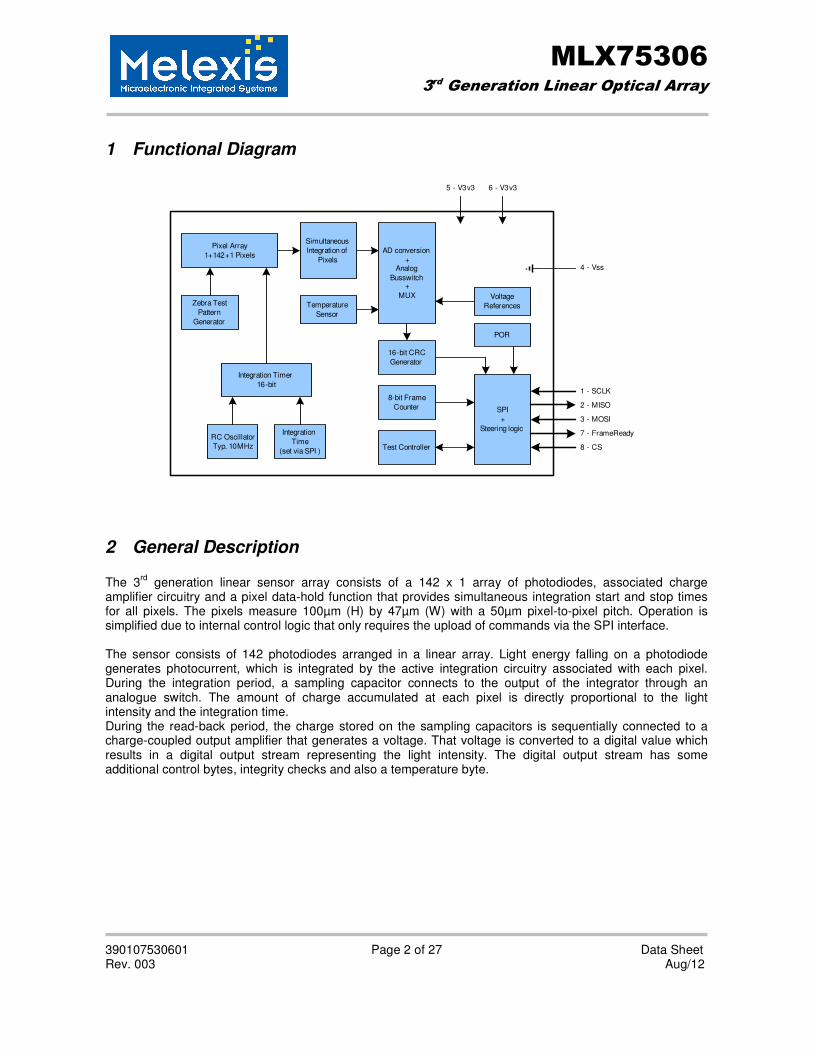
1 Functional Diagram
6 - V3v3
4 - Vss
Integration Timer
16-bit
RC Oscillator
Typ. 10MHz
Integration
Time
(set via SPI )
Pixel Array
1+142+1 Pixels
SPI
+
Steering logic
Simultaneous
Integration of
Pixels
3 - MOSI
2 - MISO
1 - SCLK
8 - CSTest Controller
Temperature
Sensor
AD conversion
+Analog
Busswitch+
MUX Voltage
References
16-bit CRC
Generator
8-bit Frame
Counter
Zebra Test
Pattern
Generator
POR
5 - V3v3
7 - FrameReady
2 General Description The 3
rd generation linear sensor array consists of a 142 x 1 array of photodiodes, associated charge
amplifier circuitry and a pixel data-hold function that provides simultaneous integration start and stop times for all pixels. The pixels measure 100µm (H) by 47µm (W) with a 50µm pixel-to-pixel pitch. Operation is simplified due to internal control logic that only requires the upload of commands via the SPI interface. The sensor consists of 142 photodiodes arranged in a linear array. Light energy falling on a photodiode generates photocurrent, which is integrated by the active integration circuitry associated with each pixel. During the integration period, a sampling capacitor connects to the output of the integrator through an analogue switch. The amount of charge accumulated at each pixel is directly proportional to the light intensity and the integration time. During the read-back period, the charge stored on the sampling capacitors is sequentially connected to a charge-coupled output amplifier that generates a voltage. That voltage is converted to a digital value which results in a digital output stream representing the light intensity. The digital output stream has some additional control bytes, integrity checks and also a temperature byte.
MLX75306 3rd Generation Linear Optical Array
390107530601 Page 3 of 27 Data Sheet Rev. 003 Aug/12
Table of Contents
1 Functional Diagram .................................................................................................... 2
2 General Description ................................................................................................... 2
3 Glossary of Terms ...................................................................................................... 4
4 Pin Definitions and Descriptions .............................................................................. 4
5 Absolute Maximum Ratings ...................................................................................... 4
6 Electrical Specifications ............................................................................................ 5
7 Sensor Specific Specifications ................................................................................. 5
8 Optical Specifications ................................................................................................ 6
9 Pixel Geometry ........................................................................................................... 7
10 Digital functionality .................................................................................................... 8
10.1 General description ......................................................................................................... 8
10.2 Detailed explanation of SPI Instruction Words .............................................................. 10
10.2.1 CR – Chip Reset Command ................................................................................................... 10
10.2.2 RT/WT – Read/Write Thresholds ........................................................................................... 10
10.2.3 SI/SIL – Start Integration (Long) Command ........................................................................... 12
10.2.4 ROx – Read-Out Command (x bit) ......................................................................................... 13
10.2.5 TZ1 – Test Zebra Pattern 1 .................................................................................................... 19
10.2.6 TZ2 - Test Zebra Pattern 2 ..................................................................................................... 20
10.2.7 TZ12 - Test Zebra Pattern 12 ................................................................................................. 20
10.2.8 TZ0 – Test Zebra Pattern 0 .................................................................................................... 20
10.2.9 SM - Sleep Mode .................................................................................................................... 20
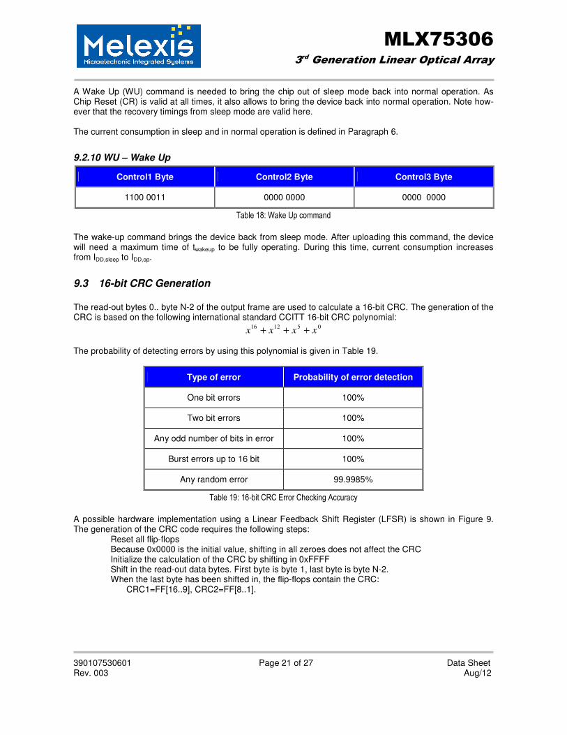
10.2.10 WU – Wake Up ...................................................................................................................... 21
10.3 16-bit CRC Generation ................................................................................................. 21
10.4 Temperature Sensor ..................................................................................................... 23
11 Global Timing Diagram ............................................................................................ 24
12 Applications Information ......................................................................................... 24
13 SO16 Open Cavity Package information ................................................................ 25
14 Standard information regarding manufacturability of Melexis products with different soldering processes ................................................................................. 26
15 ESD Precautions ...................................................................................................... 26
16 Disclaimer ................................................................................................................. 27
MLX75306 3rd Generation Linear Optical Array
390107530601 Page 4 of 27 Data Sheet Rev. 003 Aug/12
3 Glossary of Terms Following abbreviations are used in this document: ADC: Analog-to-Digital Converter CRC: Cyclic Redundancy Code DAC: Digital-to-Analog Converter ESD: Electro-Static Discharge LFSR: Linear Feedback Shift Register LSB: Least Significant Bit MSB: Most Significant Bit POR: Power-On-Reset SPI: Serial Peripheral Interface
4 Pin Definitions and Descriptions
Pin Number
Pin Name Description Type
1 SCLK SPI clock input Digital input
2 MISO SPI data output Digital push-pull output buffer with tristate
3 MOSI SPI data input Digital input
4 Vss Ground Ground
5 V3v3 3.3V Power Supply Supply
6 V3v3 3.3V Power Supply Supply
7 FrameReady End-of-integration-cycle indication Digital push-pull output
8 CS SPI chip select Digital input
9..16 - - Floating/Ground
5 Absolute Maximum Ratings All voltages are referenced to Vss.
Symbol Rating Value Unit
V3V3 3.3V Supply voltage -0.3 to 3.6 V
Vin DC Input Voltage -0.3 to V3V3+0.3V V
Vout DC Output Voltage -0.3 to V3V3+0.3V V
Iin DC Input Current, per Pin ±10 mA
Iout DC Output Current, per Pin ±20 mA
TStg Storage Temperature Range, TS -50 to 150 °C
VESD ESD Sensitivity (Human Body Model according to CDF-AEC-Q100-002)
3 kV
Exceeding the absolute maximum ratings may cause permanent damage. Exposure to absolute-maximum-rated conditions for extended periods may affect device reliability.
MLX75306 3rd Generation Linear Optical Array
390107530601 Page 5 of 27 Data Sheet Rev. 003 Aug/12
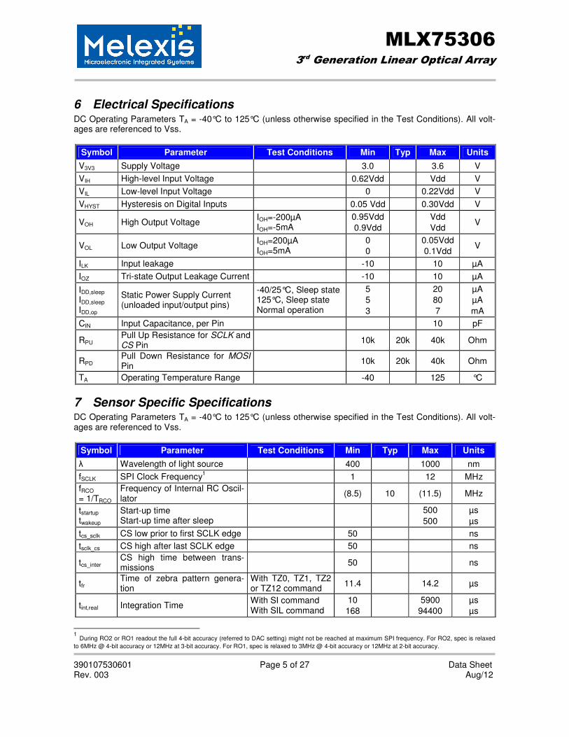
6 Electrical Specifications DC Operating Parameters TA = -40°C to 125°C (unless otherwise specified in the Test Conditions). All volt-ages are referenced to Vss.
Symbol Parameter Test Conditions Min Typ Max Units
V3V3 Supply Voltage 3.0 3.6 V
VIH High-level Input Voltage 0.62Vdd Vdd V
VIL Low-level Input Voltage 0 0.22Vdd V
VHYST Hysteresis on Digital Inputs 0.05 Vdd 0.30Vdd V
VOH High Output Voltage IOH=-200µA IOH=-5mA
0.95Vdd
0.9Vdd
Vdd
Vdd V
VOL Low Output Voltage IOH=200µA IOH=5mA
0
0
0.05Vdd
0.1Vdd V
ILK Input leakage -10 10 µA
IOZ Tri-state Output Leakage Current -10 10 µA
IDD,sleep
IDD,sleep
IDD,op
Static Power Supply Current (unloaded input/output pins)
-40/25°C, Sleep state 125°C, Sleep state Normal operation
5
5
3
20
80
7
µA
µA
mA
CIN Input Capacitance, per Pin 10 pF
RPU Pull Up Resistance for SCLK and CS Pin
10k 20k 40k Ohm
RPD Pull Down Resistance for MOSI Pin
10k 20k 40k Ohm
TA Operating Temperature Range -40 125 °C
7 Sensor Specific Specifications DC Operating Parameters TA = -40°C to 125°C (unless otherwise specified in the Test Conditions). All volt-ages are referenced to Vss.
Symbol Parameter Test Conditions Min Typ Max Units
λ Wavelength of light source 400 1000 nm
fSCLK SPI Clock Frequency1 1 12 MHz
fRCO
= 1/TRCO
Frequency of Internal RC Oscil-lator
(8.5) 10 (11.5) MHz
tstartup
twakeup
Start-up time Start-up time after sleep
500
500
µs
µs
tcs_sclk CS low prior to first SCLK edge 50 ns
tsclk_cs CS high after last SCLK edge 50 ns
tcs_inter CS high time between trans-missions
50 ns
tfr Time of zebra pattern genera-tion
With TZ0, TZ1, TZ2 or TZ12 command
11.4 14.2 µs
tint,real Integration Time With SI command With SIL command
10
168
5900
94400
µs
µs
1 During RO2 or RO1 readout the full 4-bit accuracy (referred to DAC setting) might not be reached at maximum SPI frequency. For RO2, spec is relaxed
to 6MHz @ 4-bit accuracy or 12MHz at 3-bit accuracy. For RO1, spec is relaxed to 3MHz @ 4-bit accuracy or 12MHz at 2-bit accuracy.
MLX75306 3rd Generation Linear Optical Array
390107530601 Page 6 of 27 Data Sheet Rev. 003 Aug/12
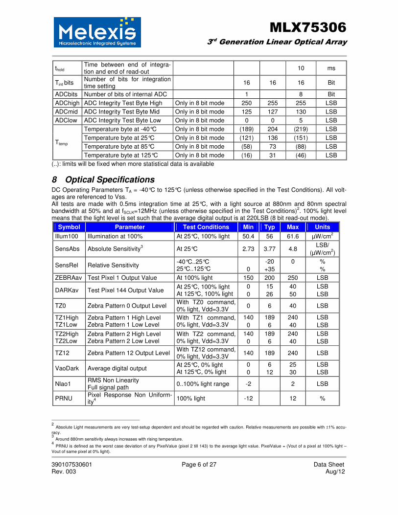
thold Time between end of integra-tion and end of read-out
10 ms
Tint bits Number of bits for integration time setting
16 16 16 Bit
ADCbits Number of bits of internal ADC 1 8 Bit
ADChigh ADC Integrity Test Byte High Only in 8 bit mode 250 255 255 LSB
ADCmid ADC Integrity Test Byte Mid Only in 8 bit mode 125 127 130 LSB
ADClow ADC Integrity Test Byte Low Only in 8 bit mode 0 0 5 LSB
Ttemp
Temperature byte at -40°C Only in 8 bit mode (189) 204 (219) LSB
Temperature byte at 25°C Only in 8 bit mode (121) 136 (151) LSB
Temperature byte at 85°C Only in 8 bit mode (58) 73 (88) LSB
Temperature byte at 125°C Only in 8 bit mode (16) 31 (46) LSB
(..): limits will be fixed when more statistical data is available
8 Optical Specifications DC Operating Parameters TA = -40°C to 125°C (unless otherwise specified in the Test Conditions). All volt-ages are referenced to Vss. All tests are made with 0.5ms integration time at 25°C, with a light source at 880nm and 80nm spectral bandwidth at 50% and at fSCLK=12MHz (unless otherwise specified in the Test Conditions)
2. 100% light level
means that the light level is set such that the average digital output is at 220LSB (8 bit read-out mode).
Symbol Parameter Test Conditions Min Typ Max Units
Illum100 Illumination at 100% At 25°C, 100% light 50.4 56 61.6 µW/cm2
SensAbs Absolute Sensitivity3 At 25°C 2.73 3.77 4.8
LSB/
(µW/cm2)
SensRel Relative Sensitivity -40°C..25°C 25°C..125°C
0
-20
+35
0
%
%
ZEBRAav Test Pixel 1 Output Value At 100% light 150 200 250 LSB
DARKav Test Pixel 144 Output Value At 25°C, 100% light At 125°C, 100% light
0
0
15
26
40
50
LSB
LSB
TZ0 Zebra Pattern 0 Output Level With TZ0 command, 0% light, Vdd=3.3V
0 6 40 LSB
TZ1High TZ1Low
Zebra Pattern 1 High Level Zebra Pattern 1 Low Level
With TZ1 command, 0% light, Vdd=3.3V
140
0
189
6
240
40
LSB
LSB
TZ2High TZ2Low
Zebra Pattern 2 High Level Zebra Pattern 2 Low Level
With TZ2 command, 0% light, Vdd=3.3V
140
0
189
6
240
40
LSB
LSB
TZ12 Zebra Pattern 12 Output Level With TZ12 command, 0% light, Vdd=3.3V
140 189 240 LSB
VaoDark Average digital output At 25°C, 0% light At 125°C, 0% light
0
0
6
12
25
30
LSB
LSB
Nlao1 RMS Non Linearity Full signal path
0..100% light range -2 2 LSB
PRNU Pixel Response Non Uniform-ity
4
100% light -12 12 %
2 Absolute Light measurements are very test-setup dependent and should be regarded with caution. Relative measurements are possible with ±1% accu-
racy. 3 Around 880nm sensitivity always increases with rising temperature.
4 PRNU is defined as the worst case deviation of any PixelValue (pixel 2 till 143) to the average light value. PixelValue = (Vout of a pixel at 100% light –
Vout of same pixel at 0% light).
MLX75306 3rd Generation Linear Optical Array
390107530601 Page 7 of 27 Data Sheet Rev. 003 Aug/12
DSNU Dark Signal Non Uniformity5 0 2 10 LSB
Vnoise RMS Noise Level
6
Full signal path 0 2 LSB
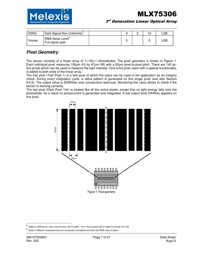
Pixel Geometry The sensor consists of a linear array of 1+142+1 photodiodes. The pixel geometry is shown in Figure 1. Each individual pixel measures 100µm (H) by 47µm (W) with a 50µm pixel-to-pixel pitch. There are 142 ac-tive pixels which can be used to measure the light intensity. One extra pixel, each with a special functionality, is added to both ends of the linear array. The first pixel (Test Pixel 1) is a test pixel of which the value can be used in the application as an integrity check. During every integration cycle, a zebra pattern is generated on this single pixel (see also Section 9.2.5). The output value is ZEBRAav over consecutive read-outs. Monitoring this value allows to check if the sensor is working correctly. The last pixel (Dark Pixel 144) is treated like all the active pixels, except that no light energy falls onto the photodiode. As a result no photocurrent is generated and integrated. A low output level DARKav appears on this pixel.
Te
st
Pix
el 1
Acti
ve
Pix
el
2
Acti
ve
Pix
el
3
Acti
ve
Pix
el
14
2
Acti
ve
Pix
el
14
3
Da
rk P
ixe
l 14
4
Ac
tiv
e P
ixe
l 72
Ac
tiv
e P
ixe
l 73
10
0µ
m
50µm
47µm
Figure 1: Pixel geometry
5 DSNU is defined as: (max Vout of pixel i @ 0% light) - (min Vout of pixel j @ 0% light) for pixels 2 to 143.
6 Noise: 4 different measurements are compared, normalized and then the RMS value is taken.
MLX75306 3rd Generation Linear Optical Array
390107530601 Page 8 of 27 Data Sheet Rev. 003 Aug/12
9 Digital functionality
9.1 General description
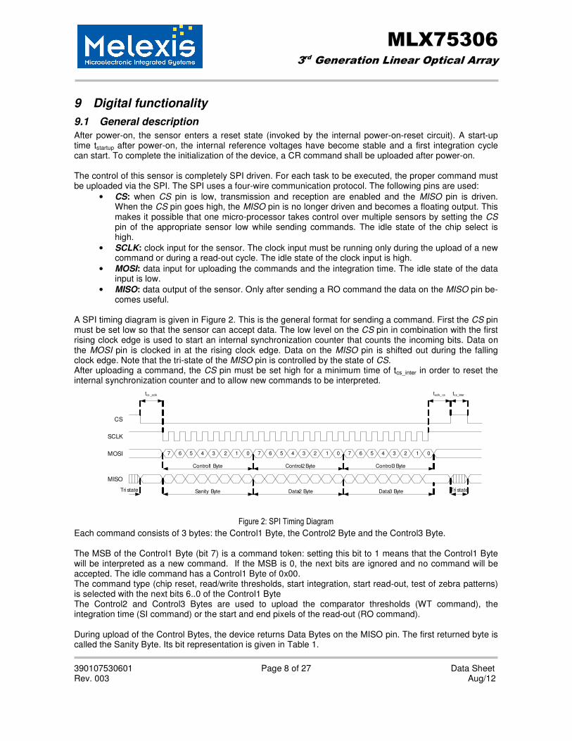
After power-on, the sensor enters a reset state (invoked by the internal power-on-reset circuit). A start-up time tstartup after power-on, the internal reference voltages have become stable and a first integration cycle can start. To complete the initialization of the device, a CR command shall be uploaded after power-on. The control of this sensor is completely SPI driven. For each task to be executed, the proper command must be uploaded via the SPI. The SPI uses a four-wire communication protocol. The following pins are used:
• CS: when CS pin is low, transmission and reception are enabled and the MISO pin is driven. When the CS pin goes high, the MISO pin is no longer driven and becomes a floating output. This makes it possible that one micro-processor takes control over multiple sensors by setting the CS pin of the appropriate sensor low while sending commands. The idle state of the chip select is high.
• SCLK: clock input for the sensor. The clock input must be running only during the upload of a new command or during a read-out cycle. The idle state of the clock input is high.
• MOSI: data input for uploading the commands and the integration time. The idle state of the data input is low.
• MISO: data output of the sensor. Only after sending a RO command the data on the MISO pin be-comes useful.
A SPI timing diagram is given in Figure 2. This is the general format for sending a command. First the CS pin must be set low so that the sensor can accept data. The low level on the CS pin in combination with the first rising clock edge is used to start an internal synchronization counter that counts the incoming bits. Data on the MOSI pin is clocked in at the rising clock edge. Data on the MISO pin is shifted out during the falling clock edge. Note that the tri-state of the MISO pin is controlled by the state of CS. After uploading a command, the CS pin must be set high for a minimum time of tcs_inter in order to reset the internal synchronization counter and to allow new commands to be interpreted.
Control1 Byte Control2 Byte Control3 Byte
CS
SCLK
MOSI
MISO
7 6 5 4 3 2 1 0 2 1 0 7 6 5 4 3 2 1 034567
Tri state Tri state
tcs _sclk tsclk_ cs tcs_inter
Sanity Byte Data2 Byte Data3 Byte
Figure 2: SPI Timing Diagram
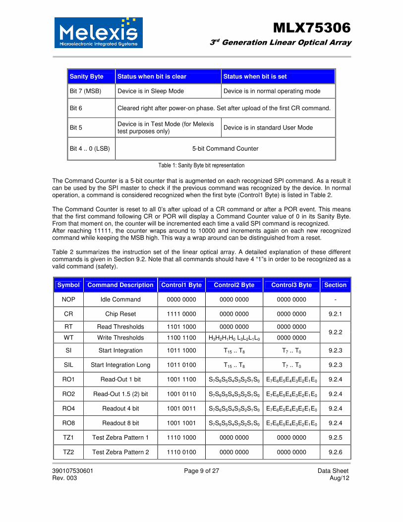
Each command consists of 3 bytes: the Control1 Byte, the Control2 Byte and the Control3 Byte. The MSB of the Control1 Byte (bit 7) is a command token: setting this bit to 1 means that the Control1 Byte will be interpreted as a new command. If the MSB is 0, the next bits are ignored and no command will be accepted. The idle command has a Control1 Byte of 0x00. The command type (chip reset, read/write thresholds, start integration, start read-out, test of zebra patterns) is selected with the next bits 6..0 of the Control1 Byte The Control2 and Control3 Bytes are used to upload the comparator thresholds (WT command), the integration time (SI command) or the start and end pixels of the read-out (RO command). During upload of the Control Bytes, the device returns Data Bytes on the MISO pin. The first returned byte is called the Sanity Byte. Its bit representation is given in Table 1.
MLX75306 3rd Generation Linear Optical Array
390107530601 Page 9 of 27 Data Sheet Rev. 003 Aug/12
Sanity Byte Status when bit is clear Status when bit is set
Bit 7 (MSB) Device is in Sleep Mode Device is in normal operating mode
Bit 6 Cleared right after power-on phase. Set after upload of the first CR command.
Bit 5 Device is in Test Mode (for Melexis test purposes only)
Device is in standard User Mode
Bit 4 .. 0 (LSB) 5-bit Command Counter
Table 1: Sanity Byte bit representation
The Command Counter is a 5-bit counter that is augmented on each recognized SPI command. As a result it can be used by the SPI master to check if the previous command was recognized by the device. In normal operation, a command is considered recognized when the first byte (Control1 Byte) is listed in Table 2. The Command Counter is reset to all 0’s after upload of a CR command or after a POR event. This means that the first command following CR or POR will display a Command Counter value of 0 in its Sanity Byte. From that moment on, the counter will be incremented each time a valid SPI command is recognized. After reaching 11111, the counter wraps around to 10000 and increments again on each new recognized command while keeping the MSB high. This way a wrap around can be distinguished from a reset. Table 2 summarizes the instruction set of the linear optical array. A detailed explanation of these different commands is given in Section 9.2. Note that all commands should have 4 “1”s in order to be recognized as a valid command (safety).
Symbol Command Description Control1 Byte Control2 Byte Control3 Byte Section
NOP Idle Command 0000 0000 0000 0000 0000 0000 -
CR Chip Reset 1111 0000 0000 0000 0000 0000 9.2.1
RT Read Thresholds 1101 1000 0000 0000 0000 0000 9.2.2
WT Write Thresholds 1100 1100 H3H2H1H0 L3L2L1L0 0000 0000
SI Start Integration 1011 1000 T15 .. T8 T7 .. T0 9.2.3
SIL Start Integration Long 1011 0100 T15 .. T8 T7 .. T0 9.2.3
RO1 Read-Out 1 bit 1001 1100 S7S6S5S4S3S2S1S0 E7E6E5E4E3E2E1E0 9.2.4
RO2 Read-Out 1.5 (2) bit 1001 0110 S7S6S5S4S3S2S1S0 E7E6E5E4E3E2E1E0 9.2.4
RO4 Readout 4 bit 1001 0011 S7S6S5S4S3S2S1S0 E7E6E5E4E3E2E1E0 9.2.4
RO8 Readout 8 bit 1001 1001 S7S6S5S4S3S2S1S0 E7E6E5E4E3E2E1E0 9.2.4
TZ1 Test Zebra Pattern 1 1110 1000 0000 0000 0000 0000 9.2.5
TZ2 Test Zebra Pattern 2 1110 0100 0000 0000 0000 0000 9.2.6
MLX75306 3rd Generation Linear Optical Array
390107530601 Page 10 of 27 Data Sheet Rev. 003 Aug/12
TZ12 Test Zebra Pattern 1&2 1110 0010 0000 0000 0000 0000 9.2.7
TZ0 Test Zebra Pattern 0 1110 0001 0000 0000 0000 0000 9.2.8
SM Sleep Mode 1100 0110 0000 0000 0000 0000 9.2.9
WU Wake Up 1100 0011 0000 0000 0000 0000 9.2.10
Table 2: Instruction set of the linear optical array
9.2 Detailed explanation of SPI Instruction Words
9.2.1 CR – Chip Reset Command
After sending a Chip Reset command as defined in Table 3, the sensor returns to a state as it is after power-up. This command can be uploaded at every time, even during a read-out cycle, provided that the internal synchronization counter is reset. This is done by setting the CS pin high for a time tcs_inter. Note that a CR command is required after POR to complete the initialization cycle.
Control1 Byte Control2 Byte Control3 Byte
1111 0000 0000 0000 0000 0000
Table 3: Chip Reset Command When a CR command is uploaded during sleep mode, the device is automatically taken out of sleep mode again. Note that this requires a time twakeup before the internal analog circuitry is fully set up again.
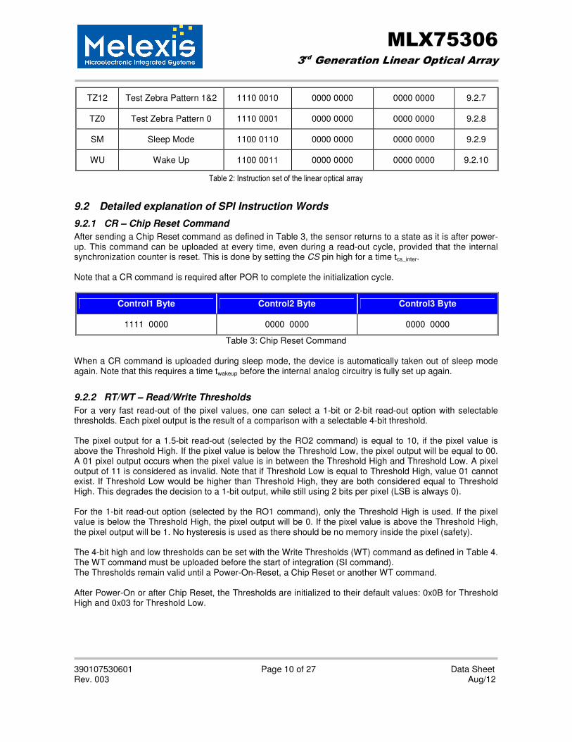
9.2.2 RT/WT – Read/Write Thresholds
For a very fast read-out of the pixel values, one can select a 1-bit or 2-bit read-out option with selectable thresholds. Each pixel output is the result of a comparison with a selectable 4-bit threshold. The pixel output for a 1.5-bit read-out (selected by the RO2 command) is equal to 10, if the pixel value is above the Threshold High. If the pixel value is below the Threshold Low, the pixel output will be equal to 00. A 01 pixel output occurs when the pixel value is in between the Threshold High and Threshold Low. A pixel output of 11 is considered as invalid. Note that if Threshold Low is equal to Threshold High, value 01 cannot exist. If Threshold Low would be higher than Threshold High, they are both considered equal to Threshold High. This degrades the decision to a 1-bit output, while still using 2 bits per pixel (LSB is always 0). For the 1-bit read-out option (selected by the RO1 command), only the Threshold High is used. If the pixel value is below the Threshold High, the pixel output will be 0. If the pixel value is above the Threshold High, the pixel output will be 1. No hysteresis is used as there should be no memory inside the pixel (safety). The 4-bit high and low thresholds can be set with the Write Thresholds (WT) command as defined in Table 4. The WT command must be uploaded before the start of integration (SI command). The Thresholds remain valid until a Power-On-Reset, a Chip Reset or another WT command. After Power-On or after Chip Reset, the Thresholds are initialized to their default values: 0x0B for Threshold High and 0x03 for Threshold Low.
MLX75306 3rd Generation Linear Optical Array
390107530601 Page 11 of 27 Data Sheet Rev. 003 Aug/12
Control1 Byte Control2 Byte Control3 Byte
1100 1100 H3H2H1H0 L3L2L1L0 0000 0000
Threshold High: H3H2H1H0
2-bit read-out option: sets the higher threshold 1-bit read-out option: sets the comparator threshold
Threshold Low: L3L2L1L0
2-bit read-out option: sets the lower threshold 1-bit read-out option: not used in this read-out option
Table 4: Write Thresholds Command Writing these thresholds translates in storing the value into a register that is directly connected to the DAC’s. This means that the effect of writing is immediate and hence should not happen during RO. The thresholds cannot be written in between SI and RO.
1.5 bit ADC
DAC threshold
register
Bit 7 6 5 4 3 2 1 0
H3 H2 H1 H0 L3 L2 L1 L0 dac
Read/Write R/W R/W R/W R/W R/W R/W R/W R/W
Init 1 0 1 1 0 0 1 1
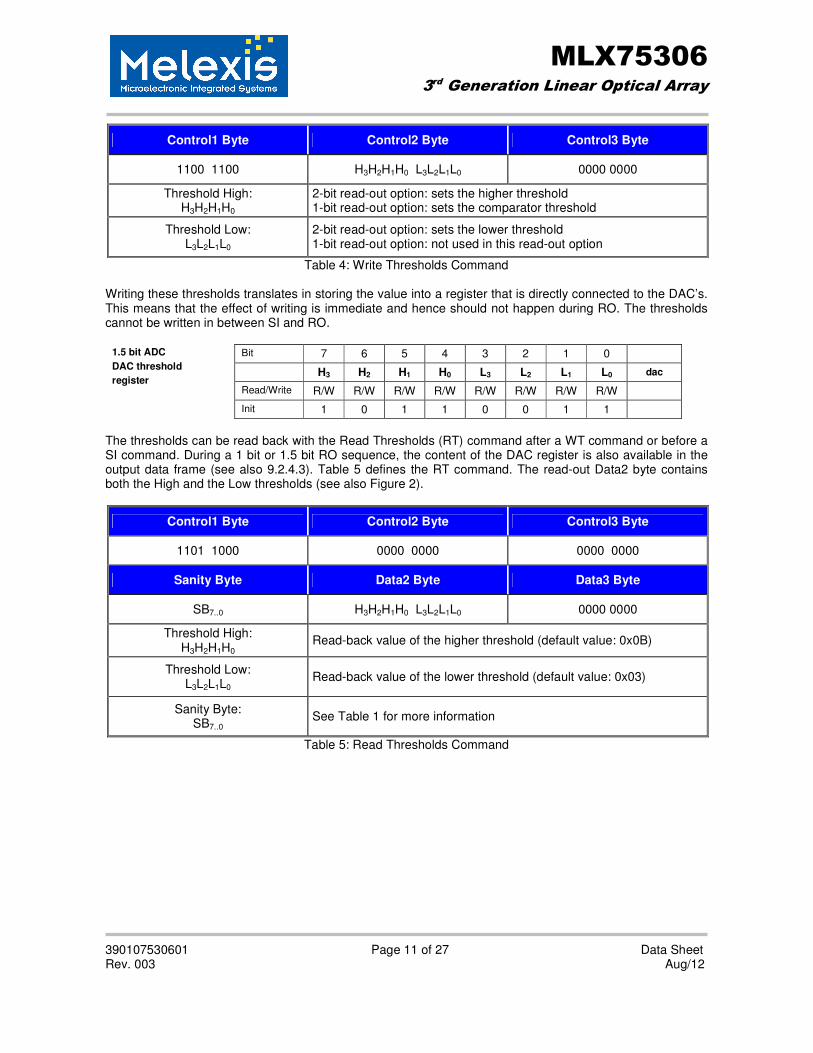
The thresholds can be read back with the Read Thresholds (RT) command after a WT command or before a SI command. During a 1 bit or 1.5 bit RO sequence, the content of the DAC register is also available in the output data frame (see also 9.2.4.3). Table 5 defines the RT command. The read-out Data2 byte contains both the High and the Low thresholds (see also Figure 2).
Control1 Byte Control2 Byte Control3 Byte
1101 1000 0000 0000 0000 0000
Sanity Byte Data2 Byte Data3 Byte
SB7..0 H3H2H1H0 L3L2L1L0 0000 0000
Threshold High: H3H2H1H0
Read-back value of the higher threshold (default value: 0x0B)
Threshold Low: L3L2L1L0
Read-back value of the lower threshold (default value: 0x03)
Sanity Byte: SB7..0
See Table 1 for more information
Table 5: Read Thresholds Command
MLX75306 3rd Generation Linear Optical Array
390107530601 Page 12 of 27 Data Sheet Rev. 003 Aug/12
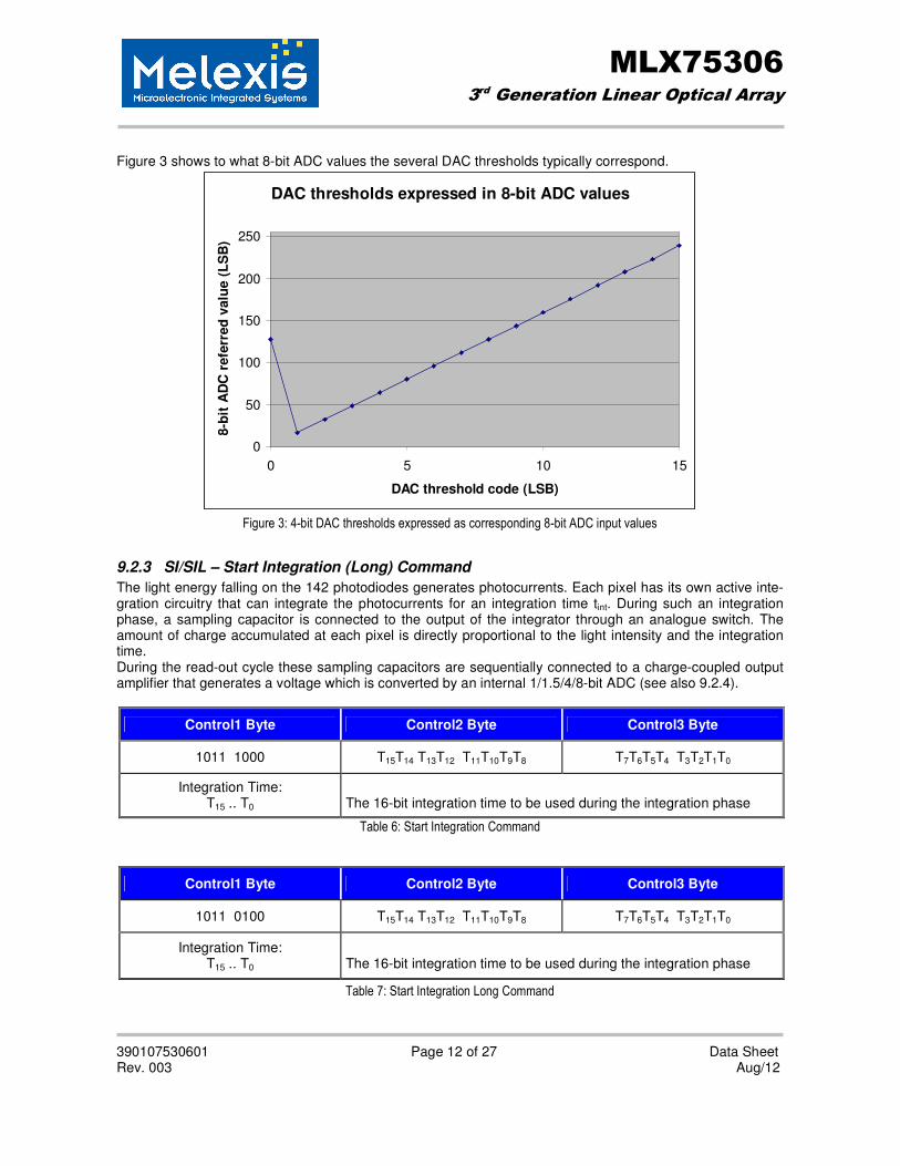
Figure 3 shows to what 8-bit ADC values the several DAC thresholds typically correspond.
Figure 3: 4-bit DAC thresholds expressed as corresponding 8-bit ADC input values
9.2.3 SI/SIL – Start Integration (Long) Command
The light energy falling on the 142 photodiodes generates photocurrents. Each pixel has its own active inte-gration circuitry that can integrate the photocurrents for an integration time tint. During such an integration phase, a sampling capacitor is connected to the output of the integrator through an analogue switch. The amount of charge accumulated at each pixel is directly proportional to the light intensity and the integration time. During the read-out cycle these sampling capacitors are sequentially connected to a charge-coupled output amplifier that generates a voltage which is converted by an internal 1/1.5/4/8-bit ADC (see also 9.2.4).
Control1 Byte Control2 Byte Control3 Byte
1011 1000 T15T14 T13T12 T11T10T9T8 T7T6T5T4 T3T2T1T0
Integration Time: T15 .. T0
The 16-bit integration time to be used during the integration phase
Table 6: Start Integration Command
Control1 Byte Control2 Byte Control3 Byte
1011 0100 T15T14 T13T12 T11T10T9T8 T7T6T5T4 T3T2T1T0
Integration Time: T15 .. T0
The 16-bit integration time to be used during the integration phase
Table 7: Start Integration Long Command
DAC thresholds expressed in 8-bit ADC values
0
50
100
150
200
250
0 5 10 15
DAC threshold code (LSB)
8-b
it A
DC
refe
rred
valu
e (
LS
B)
MLX75306 3rd Generation Linear Optical Array
390107530601 Page 13 of 27 Data Sheet Rev. 003 Aug/12
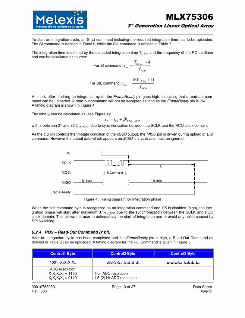
To start an integration cycle, an SI(L) command including the required integration time has to be uploaded. The SI command is defined in Table 6, while the SIL command is defined in Table 7. The integration time is defined by the uploaded integration time T[15..0] and the frequency of the RC oscillator and can be calculated as follows:
For SI command:
RCOf
Tt
4]0..15[
int
−=
For SIL command:
RCOf
Tt
1116]0..15[
int
+=
A time tfr after finishing an integration cycle, the FrameReady pin goes high, indicating that a read-out com-mand can be uploaded. A read-out command will not be accepted as long as the FrameReady pin is low. A timing diagram is shown in Figure 4. The time tfr can be calculated as (see Figure 4):
RCOCLKfr ttt_int
β+=
with β between 21 and 22 tCLK_RCO, due to synchronization between the SCLK and the RCO clock domain. As the CS pin controls the tri-state condition of the MISO output, the MISO pin is driven during upload of a SI command. However the output data which appears on MISO is invalid and must be ignored.
CS
SCLK
MOSI
MISOTri state Tri state
FrameReady
SI Command
tfr
Figure 4: Timing diagram for Integration phase
When the first command byte is recognized as an integration command and CS is disabled (high), the inte-gration phase will start after maximum 3 tCLK_RCO due to the synchronization between the SCLK and RCO clock domain. This allows the user to define/delay the start of integration and to avoid any noise caused by SPI switching.
9.2.4 ROx – Read-Out Command (x bit)
After an integration cycle has been completed and the FrameReady pin is high, a Read-Out Command as defined in Table 8 can be uploaded. A timing diagram for the RO Command is given in Figure 5.
Control1 Byte Control2 Byte Control3 Byte
1001 X3X2X1X0 S7S6S5S4 S3S2S1S0 E7E6E5E4 E3E2E1E0
ADC resolution X3X2X1X0 = 1100 X3X2X1X0 = 0110
1-bit ADC resolution 1.5-(2) bit ADC resolution
MLX75306 3rd Generation Linear Optical Array
390107530601 Page 14 of 27 Data Sheet Rev. 003 Aug/12
X3X2X1X0 = 0011 X3X2X1X0 = 1001
4-bit ADC resolution 8-bit ADC resolution
Start pixel: S7S6S5S4 S3S2S1S0
Starting pixel index, from 2 till 143
End pixel: E7E6E5E4 E3E2E1E0
Ending pixel index, from 2 till 143
Table 8: Read-Out Command
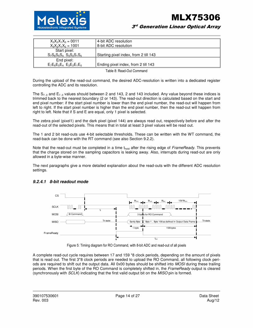
During the upload of the read-out command, the desired ADC-resolution is written into a dedicated register controlling the ADC and its resolution. The S7..0 and E7..0 values should between 2 and 143, 2 and 143 included. Any value beyond these indices is trimmed back to the nearest boundary (2 or 143). The read-out direction is calculated based on the start and end pixel number: if the start pixel number is lower than the end pixel number, the read-out will happen from left to right. If the start pixel number is higher than the end pixel number, then the read-out will happen from right to left. Note that if S and E are equal, only 1 pixel is selected. The zebra pixel (pixel1) and the dark pixel (pixel 144) are always read out, respectively before and after the read-out of the selected pixels. This means that in total at least 3 pixel values will be read out. The 1 and 2 bit read-outs use 4-bit selectable thresholds. These can be written with the WT command, the read-back can be done with the RT command (see also Section 9.2.2). Note that the read-out must be completed in a time thold after the rising edge of FrameReady. This prevents that the charge stored on the sampling capacitors is leaking away. Also, interrupts during read-out are only allowed in a byte-wise manner. The next paragraphs give a more detailed explanation about the read-outs with the different ADC resolution settings.
9.2.4.1 8-bit readout mode
CS
SCLK
MOSI
MISOTri state Tri state
FrameReady
3 bytes for RO Command
8tsclk 156*8tsclk
Byte 1 .. Byte 158 as defined in Output Data Frame
158 bytes
SI Command
tfr
8tsclk 8tsclk
Sanity Byte
1 byte
thold
Figure 5: Timing diagram for RO Command, with 8-bit ADC and read-out of all pixels
A complete read-out cycle requires between 17 and 159 *8 clock periods, depending on the amount of pixels that is read out. The first 3*8 clock periods are needed to upload the RO Command, all following clock peri-ods are required to shift out the output data. All 0x00 bytes should be shifted into MOSI during these trailing periods. When the first byte of the RO Command is completely shifted in, the FrameReady output is cleared (synchronously with SCLK) indicating that the first valid output bit on the MISO pin is formed.
MLX75306 3rd Generation Linear Optical Array
390107530601 Page 15 of 27 Data Sheet Rev. 003 Aug/12
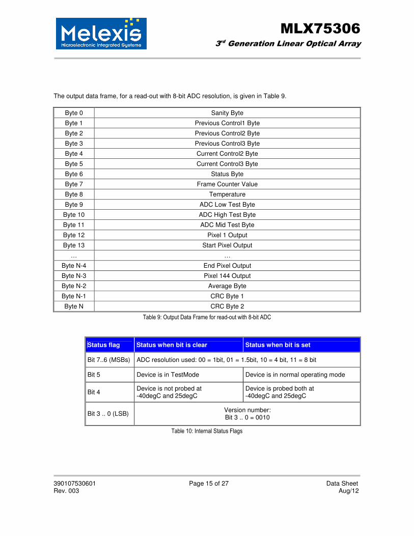
The output data frame, for a read-out with 8-bit ADC resolution, is given in Table 9.
Byte 0 Sanity Byte
Byte 1 Previous Control1 Byte
Byte 2 Previous Control2 Byte
Byte 3 Previous Control3 Byte
Byte 4 Current Control2 Byte
Byte 5 Current Control3 Byte
Byte 6 Status Byte
Byte 7 Frame Counter Value
Byte 8 Temperature
Byte 9 ADC Low Test Byte
Byte 10 ADC High Test Byte
Byte 11 ADC Mid Test Byte
Byte 12 Pixel 1 Output
Byte 13 Start Pixel Output
… …
Byte N-4 End Pixel Output
Byte N-3 Pixel 144 Output
Byte N-2 Average Byte
Byte N-1 CRC Byte 1
Byte N CRC Byte 2
Table 9: Output Data Frame for read-out with 8-bit ADC
Status flag Status when bit is clear Status when bit is set
Bit 7..6 (MSBs) ADC resolution used: 00 = 1bit, 01 = 1.5bit, 10 = 4 bit, 11 = 8 bit
Bit 5 Device is in TestMode Device is in normal operating mode
Bit 4 Device is not probed at -40degC and 25degC
Device is probed both at -40degC and 25degC
Bit 3 .. 0 (LSB) Version number: Bit 3 .. 0 = 0010
Table 10: Internal Status Flags
MLX75306 3rd Generation Linear Optical Array
390107530601 Page 16 of 27 Data Sheet Rev. 003 Aug/12
A total of N bytes is read out, were N is a function of the start and end pixel index given by the RO command (S and E are in the range 2..143):
1710..70..7
++−= ESN
• Byte 0: The first output byte is the Sanity Byte discussed in Table 1.
• Bytes 1, 2, 3: These bytes contain the Control1, Control2 and Control3 bytes that were used in the previous command (i.e. SI, TZ1, TZ2, TZ12 or TZ0).
• Byte 4, 5: These bytes contain the Control2 and Control3 bytes that were used for the current readout command.
• Byte 6: The Status Byte (MSB first, LSB last) contains some internal status flags as defined in Ta-ble 10.
• Byte 7: This byte (MSB first, LSB last) represents the value of an 8-bit Frame Counter and associ-ates an identical frame number to each output frame (for up to 256 frames). The first read-out cy-cle after power-up has a Frame Counter Value of 0x00. At the end of each read-out cycle the Frame Counter is incremented. When 0xFF is reached, the Counter starts again counting at 0x00. At any moment the Frame Counter can be cleared by sending a CR command.
• Byte 8: This byte is the AD converted output voltage of the temperature sensor (MSB first, LSB last). See Section 9.4 for more details about the temperature sensor.
• Bytes 9, 10, 11: These 3 bytes (MSB first, LSB last) can be used to check the ADC integrity. Dur-ing each 8-bit read-out cycle three ADC reference voltages are converted:
- ADC Low: minimum of the ADC range - ADC High: typical 1/2 of the ADC range - ADC Mid: maximum of the ADC range
• Byte 12: This byte is the AD converted output value of the zebra pixel (pixel1 – MSB first, LSB last).
• Bytes 13..N-4: The 8-bit AD converted output value of all selected pixels, starting with the pixel addressed by S7..0 and ending with that addressed by E7..0.
• Byte N-3: This byte is the AD converted output value of the dark pixel (pixel144 – MSB first, LSB last).
• Byte N-2: The Average Byte contains the average value of bytes 13..N-4 (all active pixels that are read-out), within a tolerance of +/-1LSB.
• Bytes N-1, N: A 16-bit CRC over all the output bytes 0..N-2 is included in order to have a detection mechanism for transmission errors. Section 9.3 explains how the CRC is generated.
MLX75306 3rd Generation Linear Optical Array
390107530601 Page 17 of 27 Data Sheet Rev. 003 Aug/12
9.2.4.2 4-bit Readout Mode
3 bytes for RO command
CS
MOSI
SCLK
FrameReady
sanity byte
prev ctrl by te1
prev ctrl byte2
prev c trl byte3
curr c trl byte2
c urr c trlbyte3
status byte
fr .cntr. value
average byte
CRC byte1
CRC byte2MISO pix
1
pix
start
pix start
+D
pix end
- 5D
pix end
- 4D
pix end
-3D
pix end
-2D
pix end
-1 D
pix
end
pix
144
pix end
-7D
pix end
-6D Figure 6: Timing diagram for a readout command with 4-bit ADC resolution
The 4-bit readout mode is shown in Figure 6. Note that the temperature sensor output and the ADC test bytes (low, high, mid) are not available in 4-bit read-out mode. A total of N bytes is read out, were N is a function of the start and end pixel index given by the RO com-mand. N is defined by (edged brackets denote the ceiling function, S and E are in the range 2..143):
1112
10..70..7+
+
+−=
ESN
Note that the average byte remains 8 bits (both in size and number of information bits). Internally this is cal-culated by adding 4 zeroes to the pixel value, hereby bringing the problem back to an 8-bit pixel average calculation. By taking the 4 MSB’s, a 4-bit average is obtained. The output data frame, for a read-out with 4-bit ADC resolution, is given in Table 11. As every pixel is repre-sented by 4 bits, 2 pixels at a time are stored per output byte. Because of this, byte N-3 might be filled with 2 pixel values when an even number of pixels is selected, or by only 1 pixel value (first 4 bits = 4 MSB values) when an odd number of pixels is selected. As the average byte always contains 8 bits, it will not fill up the possible empty space of byte N-3 – this is filled by all zeroes.
Byte 0 Sanity Byte
Byte 1 Previous Control1 Byte
Byte 2 Previous Control2 Byte
Byte 3 Previous Control3 Byte
Byte 4 Current Control2 Byte
Byte 5 Current Control3 Byte
Byte 6 Status Byte
Byte 7 Frame Counter Value
Byte 8 Pixel 1 Output Start Pixel Output
… …
Byte N-3 End Pixel Output Pixel 144 Output
Byte N-2 Average Byte
Byte N-1 CRC Byte 1
Byte N CRC Byte 2
Table 11: Output Data Frame for read-out with 4-bit ADC
MLX75306 3rd Generation Linear Optical Array
390107530601 Page 18 of 27 Data Sheet Rev. 003 Aug/12
9.2.4.3 1.5 (2) bit and 1 bit Readout Mode
3 bytes for RO command
CS
MOSI
SCLK
FrameReady
dummybyte
prev ctrlbyte1
prev ctrlbyte2
prev ctrlbyte3
curr ctrlbyte2
curr ctrlbyte3
statusbyte
fr.cntr.value
averagebyte
CRCbyte1
CRCbyte2MISO p
ix 1 pix
sta
rt
pix
end
-
5D
pix
end
-4
D
pix
end
-3
Dp
ix
end
-2
Dp
ix
end
-D pix
end
pix
144
pix
end
-
6D
DACbyte
Figure 7: Internal timing diagram for a readout command with 1.5-bit ADC resolution
Figure 7 shows the timing diagram for a readout command when a 1.5 bit ADC resolution is requested (2 bits per pixel). A timing diagram for a 1 bit ADC resolution is similar. A total of N bytes is read out, were N is a function of the start and end pixel index given by the RO com-mand. In 1.5 bit mode it yields (edged brackets denote the ceiling function, S and E are in the range 2..143):
125.04
10..70..7+
+
+−=
ESN
In 1 bit mode it yields:
1225.08
10..70..7+
+
+−=
ESN
The output data frame, for a read-out with 1.5-bit ADC resolution, is given in Table 12. The data frame for a 1-bit ADC resolution is similar, except that 8 pixels are represented per byte.
Byte 0 Sanity Byte
Byte 1 Previous Control1 Byte
Byte 2 Previous Control2 Byte
Byte 3 Previous Control3 Byte
Byte 4 Current Control2 Byte
Byte 5 Current Control3 Byte
Byte 6 DAC Byte
Byte 7 Status Byte
Byte 8 Frame Counter Value
Byte 9 Pixel 1 Start Pixel Start+1D Pixel Start+2D Pixel
… …
Byte N-3 End-2D Pixel End-1D Pixel End Pixel Pixel 144
Byte N-2 Average Byte
Byte N-1 CRC Byte 1
Byte N CRC Byte 2
Table 12: Output Data Frame for read-out with 1.5-bit ADC
MLX75306 3rd Generation Linear Optical Array
390107530601 Page 19 of 27 Data Sheet Rev. 003 Aug/12
As every pixel is represented by 2 bits, 4 pixels at a time are stored per output byte. Because of this, byte N-3 might be filled with 1, 2, 3 or 4 pixel values, depending on the amount of pixels to be read out. As the aver-age byte always contains 8 bits, it will not fill up the possible empty space of byte N-3. As the pixels values will be moved to the left of that byte N-3 (MSB’s filled first), the unused LSB’s are filled up with zeroes. To allow a correct average byte calculation, only pixel values 00, 01 and 10 are allowed in a 1.5 bit read-out mode. This makes value 11 impossible. Note that the average byte remains 8 bits (both in size and number of information bits). Internally this is calculated by adding 6 or 7 zeroes (for 1.5 or 1 bit read-out mode) to the pixel sum, hereby bringing the problem back to an 8-bit pixel average calculation. Note that the byte representation for 1.5 and 1 bit mode is similar to that of 8 bit mode. In 1.5 or 1 bit mode however one extra byte is read out, namely byte 6 with the DAC values that are used as thresholds.
9.2.5 TZ1 – Test Zebra Pattern 1
Control1 Byte Control2 Byte Control3 Byte
1110 1000 0000 0000 0000 0000
Table 13: Test Zebra Pattern 1 Command This command can be used as an integrity check for all odd pixels: all odd pixels 1, 3, 5, .., 143 will return a high value TZ1High, all even pixels 2, 4, .., 144 will return a low value TZ1Low. The sampling capacitors connected to the output of the integration amplifiers associated with the odd pixels are charged with the same amount of charge in order to simulate an integrated photocurrent. During a read-out cycle, the charge stored on the sampling capacitors is sequentially connected to a charge-coupled output amplifier that gener-ates a voltage that is converted to a digital value which results in a digital output stream representing the zebra pattern. To exclude the influence of charge due to integrated photocurrents, the TZ1, TZ2, TZ12 and TZ0 tests must be performed in dark. The TZ1, TZ2, TZ12 and TZ0 commands behaves in much the same way as a SI command. Zebra integra-tion only starts when pin CS is pulled high. The integration time used during TZ1, TZ2, TZ12 and TZ0 is fixed. The time between CS high and FrameReady high is labeled as the time tfr and is defined in Paragraph 7. The read-out can be done in the same way as when a SI command is used. The Start and End pixels, as well as the ADC resolution, are set by the appropriate option bits in the RO commands.
Figure 8 shows a zebra pattern timing diagram in which the relevant timings are indicated.
CS
SCLK
MOSI
MISOTri state Tri state
FrameReady
TZ1, TZ2, TZ12 or TZ0 Command
tfr
Figure 8: TZ1, TZ2, TZ12, TZ0 Zebra pattern timings
MLX75306 3rd Generation Linear Optical Array
390107530601 Page 20 of 27 Data Sheet Rev. 003 Aug/12
9.2.6 TZ2 - Test Zebra Pattern 2
Control1 Byte Control2 Byte Control3 Byte
1110 0100 0000 0000 0000 0000
Table 14: Test Zebra Pattern 2 Command The TZ2 command is the same as the TZ1 command but this command tests the even pixels: all odd pixels 1, 3, 5, .., 143 will return a low value TZ2Low, all even pixels 2, 4, .., 144 will return a high value TZ2High. The timing diagram for TZ2 commands is given in Figure 8. Note that this includes that the zebra pixel (pixel 1) is low in this configuration.
9.2.7 TZ12 - Test Zebra Pattern 12
Control1 Byte Control2 Byte Control3 Byte
1110 0010 0000 0000 0000 0000
Table 15: Test Zebra Pattern 12 Command This is a combination of the commands TZ1 and TZ2, all pixels are tested at the same time. All pixels 1, .. , 144 will return a high value TZ12. The timing diagram for TZ12 commands is given in Figure 8.
9.2.8 TZ0 – Test Zebra Pattern 0
Control1 Byte Control2 Byte Control3 Byte
1110 0001 0000 0000 0000 0000
Table 16: Test Zebra Pattern 0 Command This command is similar to TZ12 in the sense that it activates both odd and even zebra lines to be high. After integration however, the charge of all sampling capacitors are reset before they are read out. This means that all pixels 1, .., 144 will return a low value TZ0. This command is an easy check to make sure there are no memory effects appearing inside pixels. The timing diagram for TZ0 commands is given in Figure 8. Note that the value of the Temperature byte is invalid in a TZ0 test pattern (in combination with the 8-bit read-out mode). The output value will be similar to the value of a dark pixel (VaoDark).
9.2.9 SM - Sleep Mode
Control1 Byte Control2 Byte Control3 Byte
1100 0110 0000 0000 0000 0000
Table 17: Sleep Mode command
In sleep mode, the total dc power consumption of the device is lowered drastically. This means that all ana-log circuitry, including the RCO and the ADC, are shutdown during this mode.
MLX75306 3rd Generation Linear Optical Array
390107530601 Page 21 of 27 Data Sheet Rev. 003 Aug/12
A Wake Up (WU) command is needed to bring the chip out of sleep mode back into normal operation. As Chip Reset (CR) is valid at all times, it also allows to bring the device back into normal operation. Note how-ever that the recovery timings from sleep mode are valid here. The current consumption in sleep and in normal operation is defined in Paragraph 6.
9.2.10 WU – Wake Up
Control1 Byte Control2 Byte Control3 Byte
1100 0011 0000 0000 0000 0000
Table 18: Wake Up command
The wake-up command brings the device back from sleep mode. After uploading this command, the device will need a maximum time of twakeup to be fully operating. During this time, current consumption increases from IDD,sleep to IDD,op.
9.3 16-bit CRC Generation
The read-out bytes 0.. byte N-2 of the output frame are used to calculate a 16-bit CRC. The generation of the CRC is based on the following international standard CCITT 16-bit CRC polynomial:
051216xxxx +++
The probability of detecting errors by using this polynomial is given in Table 19.
Type of error Probability of error detection
One bit errors 100%
Two bit errors 100%
Any odd number of bits in error 100%
Burst errors up to 16 bit 100%
Any random error 99.9985%
Table 19: 16-bit CRC Error Checking Accuracy
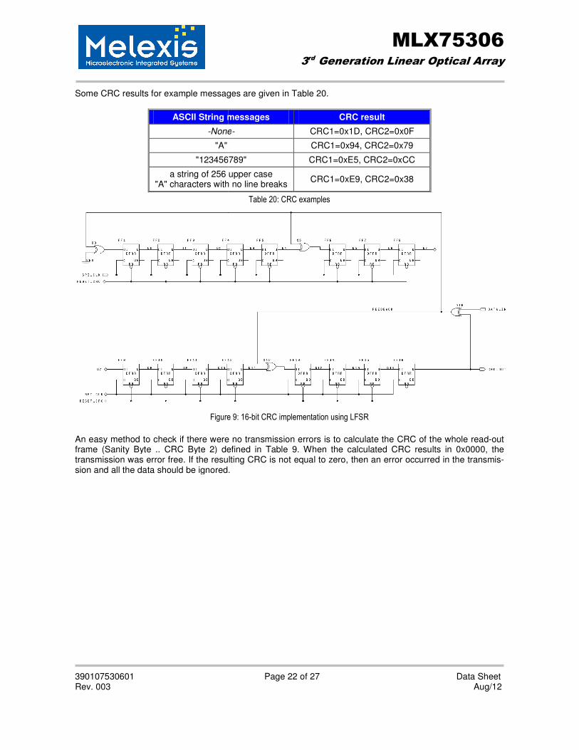
A possible hardware implementation using a Linear Feedback Shift Register (LFSR) is shown in Figure 9. The generation of the CRC code requires the following steps:
Reset all flip-flops Because 0x0000 is the initial value, shifting in all zeroes does not affect the CRC Initialize the calculation of the CRC by shifting in 0xFFFF Shift in the read-out data bytes. First byte is byte 1, last byte is byte N-2. When the last byte has been shifted in, the flip-flops contain the CRC:
CRC1=FF[16..9], CRC2=FF[8..1].
390107530601 Rev. 003
Some CRC results for example messages are given in
ASCII String messages
-None
"A"
"123456789
a string of 256 upper case "A" characters with no line breaks
Figure
An easy method to check if there were no transmission errors is to calculate the CRC of the whole readframe (Sanity Byte .. CRC Byte 2) defined in transmission was error free. If the resulting CRC is not equal to zero, then an error occurred in the transmision and all the data should be ignored.
MLX753063rd Generation Linear Optical Array
Page 22 of 27
Some CRC results for example messages are given in Table 20.
ASCII String messages CRC result
None- CRC1=0x1D, CRC2=0x0F
CRC1=0x94, CRC2=0x79
123456789" CRC1=0xE5, CRC2=0xCC
string of 256 upper case characters with no line breaks
CRC1=0xE9, CRC2=0x38
Table 20: CRC examples
Figure 9: 16-bit CRC implementation using LFSR
An easy method to check if there were no transmission errors is to calculate the CRC of the whole readByte .. CRC Byte 2) defined in Table 9. When the calculated CRC results in 0x0000, the
transmission was error free. If the resulting CRC is not equal to zero, then an error occurred in the transmision and all the data should be ignored.
MLX75306 Generation Linear Optical Array
Data Sheet Aug/12
An easy method to check if there were no transmission errors is to calculate the CRC of the whole read-out CRC results in 0x0000, the
transmission was error free. If the resulting CRC is not equal to zero, then an error occurred in the transmis-
MLX75306 3rd Generation Linear Optical Array
390107530601 Page 23 of 27 Data Sheet Rev. 003 Aug/12
9.4 Temperature Sensor
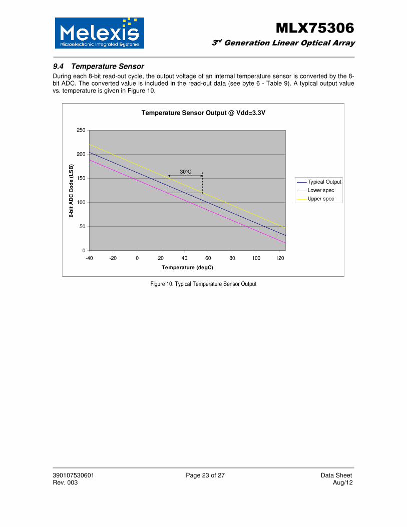
During each 8-bit read-out cycle, the output voltage of an internal temperature sensor is converted by the 8-bit ADC. The converted value is included in the read-out data (see byte 6 - Table 9). A typical output value vs. temperature is given in Figure 10.
Figure 10: Typical Temperature Sensor Output
Temperature Sensor Output @ Vdd=3.3V
0
50
100
150
200
250
-40 -20 0 20 40 60 80 100 120
Temperature (degC)
8-b
it A
DC
Co
de (
LS
B)
Typical Output
Lower spec
Upper spec
30°C
MLX75306 3rd Generation Linear Optical Array
390107530601 Page 24 of 27 Data Sheet Rev. 003 Aug/12
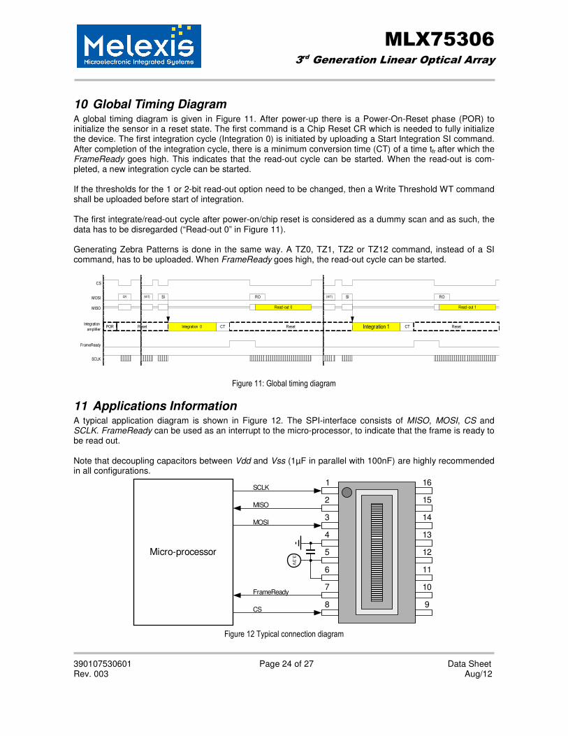
10 Global Timing Diagram A global timing diagram is given in Figure 11. After power-up there is a Power-On-Reset phase (POR) to initialize the sensor in a reset state. The first command is a Chip Reset CR which is needed to fully initialize the device. The first integration cycle (Integration 0) is initiated by uploading a Start Integration SI command. After completion of the integration cycle, there is a minimum conversion time (CT) of a time tfr after which the FrameReady goes high. This indicates that the read-out cycle can be started. When the read-out is com-pleted, a new integration cycle can be started. If the thresholds for the 1 or 2-bit read-out option need to be changed, then a Write Threshold WT command shall be uploaded before start of integration. The first integrate/read-out cycle after power-on/chip reset is considered as a dummy scan and as such, the data has to be disregarded (“Read-out 0” in Figure 11). Generating Zebra Patterns is done in the same way. A TZ0, TZ1, TZ2 or TZ12 command, instead of a SI command, has to be uploaded. When FrameReady goes high, the read-out cycle can be started.
Integration 0
RO
Read-out 0
CT Reset Integration 1
RO
Read-out 1
CT
SI SICR
Reset
MOSI
MISO
Integration
amplifier
SCLK
POR
CS
FrameReady
Reset
(WT)(WT)
Figure 11: Global timing diagram
11 Applications Information A typical application diagram is shown in Figure 12. The SPI-interface consists of MISO, MOSI, CS and SCLK. FrameReady can be used as an interrupt to the micro-processor, to indicate that the frame is ready to be read out. Note that decoupling capacitors between Vdd and Vss (1µF in parallel with 100nF) are highly recommended in all configurations.
1
2
3
4
5
6
7
8
16
15
14
13
12
11
10
9
Micro-processor
MOSI
MISO
CS
SCLK
FrameReady
3.3
V
Figure 12 Typical connection diagram
MLX75306 3rd Generation Linear Optical Array
390107530601 Page 25 of 27 Data Sheet Rev. 003 Aug/12
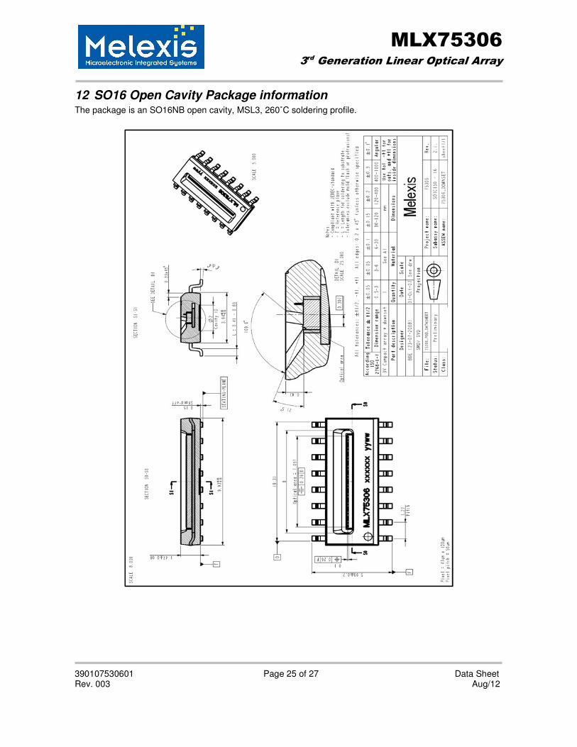
12 SO16 Open Cavity Package information The package is an SO16NB open cavity, MSL3, 260˚C soldering profile.
MLX75306 3rd Generation Linear Optical Array
390107530601 Page 26 of 27 Data Sheet Rev. 003 Aug/12
13 Standard information regarding manufacturability of Melexis products with different soldering processes
Our products are classified and qualified regarding soldering technology, solderability and moisture sensitiv-ity level according to following test methods: Reflow Soldering SMD’s (Surface Mount Devices) IPC/JEDEC J-STD-020 Moisture/Reflow Sensitivity Classification for Nonhermetic Solid State Surface Mount Devices (classification reflow profiles according to table 5-2) EIA/JEDEC JESD22-A113 Preconditioning of Nonhermetic Surface Mount Devices Prior to Reliability Testing (reflow profiles according to table 2) Wave Soldering SMD’s (Surface Mount Devices) EN60749-20 Resistance of plastic- encapsulated SMD’s to combined effect of moisture and soldering heat Solderability SMD’s (Surface Mount Devices) EIA/JEDEC JESD22-B102 and EN60749-21 Solderability For all soldering technologies deviating from above mentioned standard conditions (regarding peak tempera-ture, temperature gradient, temperature profile etc) additional classification and qualification tests have to be agreed upon with Melexis. The application of Wave Soldering for SMD’s is allowed only after consulting Melexis regarding assurance of adhesive strength between device and board. Melexis recommends reviewing on our web site the General Guidelines soldering recommendation (ht tp: / /www.melexis.com/Qual i t y_so lder ing.aspx) as wel l as tr im&form recommendat ions ( h t t p : / / w w w . m e l e x i s . c o m / A s s e t s / T r i m - a n d - f o r m - r e c o m m e n d a t i o n s - 5 5 6 5 . a s p x ) . Melexis is contributing to global environmental conservation by promoting lead free solutions. For more information on qualifications of RoHS compliant products (RoHS = European directive on the Restriction Of the use of certain Hazardous Substances) please visit the quality page on our website: http://www.melexis.com/quality.aspx
14 ESD Precautions Electronic semiconductor products are sensitive to Electro Static Discharge (ESD). Always observe Electro Static Discharge control procedures whenever handling semiconductor products.

MLX75306 3rd Generation Linear Optical Array
390107530601 Page 27 of 27 Data Sheet Rev. 003 Aug/12
15 Disclaimer Devices sold by Melexis are covered by the warranty and patent indemnification provisions appearing in its Term of Sale. Melexis makes no warranty, express, statutory, implied, or by description regarding the infor-mation set forth herein or regarding the freedom of the described devices from patent infringement. Melexis reserves the right to change specifications and prices at any time and without notice. Therefore, prior to de-signing this product into a system, it is necessary to check with Melexis for current information. This product is intended for use in normal commercial applications. Applications requiring extended temperature range, unusual environmental requirements, or high reliability applications, such as military, medical life-support or life-sustaining equipment are specifically not recommended without additional processing by Melexis for each application. The information furnished by Melexis is believed to be correct and accurate. However, Melexis shall not be liable to recipient or any third party for any damages, including but not limited to personal injury, property damage, loss of profits, loss of use, interrupt of business or indirect, special incidental or consequential damages, of any kind, in connection with or arising out of the furnishing, performance or use of the technical data herein. No obligation or liability to recipient or any third party shall arise or flow out of Melexis’ rendering of technical or other services. © 2012 Melexis NV. All rights reserved.
For the latest version of this document, go to our website at www.melexis.com
Or for additional information contact Melexis Direct:
Europe, Africa, Asia: America:
Phone: +32 1367 0495 Phone: +1 248 306 5400 E-mail: [email protected] E-mail: [email protected]
ISO/TS 16949 and ISO14001 Certified