
Datasheet - Display Solutions | Flat Panel Technology | … Panasonic VVX10F087J00 PS-01-001 - COVER...
25
The information contained in this document has been carefully researched and is, to the best of our knowledge, accurate. However, we assume no liability for any product failures or damages, immediate or consequential, resulting from the use of the information provided herein. Our products are not intended for use in systems in which failures of product could result in personal injury. All trademarks mentioned herein are property of their respective owners. All specifications are subject to change without notice. Datasheet Panasonic VVX10F087J00 PS-01-001
Transcript of Datasheet - Display Solutions | Flat Panel Technology | … Panasonic VVX10F087J00 PS-01-001 - COVER...
The information contained in this document has been carefully researched and is, to the best
of our knowledge, accurate. However, we assume no liability for any product failures or
damages, immediate or consequential, resulting from the use of the information provided
herein. Our products are not intended for use in systems in which failures of product could
result in personal injury. All trademarks mentioned herein are property of their respective
owners. All specifications are subject to change without notice.
Datasheet
Panasonic VVX10F087J00
PS-01-001

1-1/1- COVER
Panasonic Liquid Crystal Display Co.,Ltd.
VVX10F087J00
CONTENTS
No. Item Page
3-1/11 ABSOLUTE MAXIMUM RATINGS 4-1/2~2/2- DESCRIPTION
5-1/2~2/23 ELECTRICAL CHARACTERISTICS 6-1/12 INITIAL OPTICAL CHARACTERISTICS
7-1/15 INTERFACE PIN ASSIGNMENT 8-1/3~3/34 BLOCK DIAGRAM
9 PRECAUTION 12-1/3~3/3
9-1/4~4/47 LABEL FORMAT 10-1/16 INTERFACE TIMING
14-1/2~2/211 DIMENSIONAL OUTLINE13-1/2~2/210 PACKING
2601 VVX10F087J00-1 Page 1-1/1
TECHNICAL DATA
Panasonic Liquid Crystal DisplayCo.,Ltd. Date Feb.17.2016 Sheet No.ATD-11761

The following specifications are applied to the following TFT-LCD module.
Product Name : VVX10F087J00
Display size : 10 (inch)
Effective display area : (H) 220.32 × (V) 123.93 (mm)
Number of pixels : (H) 1,920 × (V) 1,080 (pixels)
Pixel pitch : (H) 0.11475 × (V) 0.11475 (mm)
Pixel density : 221 (ppi)
Color pixel arrangement : B+G+R vertical stripe
Display mode : Transmissive mode Normally black mode
Top polarizer type : Anti-Glare
Number of colors : 16,777,216 (colors)
Input signal : eDP (Ver 1.2) 2Lane
Backlight : 28 pieces of LED (LED : Light-emitting diode)
External dimensions : Typ. (H) 232.7 × (V) 138.05 × (T) 5.7 (PCB area) (mm)
Weight : Typ. 170 (TBD) (g)
ATD-11761
DESCRIPTION
General Specifications
2603 VVX10F087J00-1 Page 3-1/1Panasonic Liquid Crystal DisplayCo.,Ltd. Date Feb.17.2016 Sheet No.

1. ABSOLUTE MAXIMUM RATINGS1. 1 Environmental Absolute Maximum Ratings
Note 1) Temperature and Humidity should be applied to the glass surface of a TFT-LCD module, not tothe system installed with a module.
2) Ta≦40 ℃‥‥‥Relative humidity should be less than 85 %RH max. Dew is prohibited.Ta>40 ℃‥‥‥Relative humidity should be lower than the moisture of the 85 %RH at 40 ℃.
3) The temperature of LCD front surface would be 65 ℃ in operating, it may affect the optical characteristicshowever it does not damage the function of the module.
4) The humidity of LCD front surface would be less than 20%RH in storage, it may affect the opticalcharacteristics, however it does not damage the function of the module.
5) Long term operation (more than 1000 hours) with 60℃ or above may cause optical performance issue.However it does not damage the function of the module.
6) Long term strage (more than 1000 hours) with -25℃ or below may cause optical performance issue.
7) Vibration(Non-OP) : Frequency Random 5-500Hz, Acceleration 2.3Grms, 1 hour each axis(X,Y,Z).
8) Shock(non-OP) : Acceleration 120G 2ms, 1 time each direction(±X,±Y,±Z).
-
Corrosive Gas Not AcceptableIllumination atLCD Surface - 50,000 - 50,000 lx
m/s2 -Vibration -
Not Acceptable -
Grms
-
- -Shock - -
1),3),5),6)Humidity 2) 2)
7)8)
%RH 1),4)Temperature -20 70 -30 70 ℃
Panasonic Liquid Crystal DisplayCo.,Ltd.
ITEMOperating Storage
UNIT NOTEMin. Max. Min. Max.
Page 4-1/2Date Feb.17.2016 Sheet No.ATD-117612604 VVX10F087J00-1
Operating range
Storage range
100
80
60
40
20
20 40 60 80 0 -20 -40
Temperature(℃)
Relative Humidity(%RH)
-30 70 -10 10 30 50

1. 2 Electrical Absolute Maximum Ratings (1)TFT-LCD module
VSS = 0 V
Note1) eDP signal (Lane0_P/N, Lane1_P/N, AUX_CH_P/N)2) LED_PWM, LED_EN
ITEM SYMBOLPower Supply Voltage VDD -0.3 4.5
Min.
VLED
-0.3-0.3VI_2 2)
Input Voltage for LED driver -0.3Input Voltage for logic 1Input Voltage for logic 2
VI_1
Max. NOTEV
1)
UNIT
V1.4
VVX10F087J00-1 Page 4-2/2
V16
11.4 V
Panasonic Liquid Crystal DisplayCo.,Ltd. Date Feb.17.2016 Sheet No.ATD-117612604

2. INITIAL OPTICAL CHARACTERISTICS The following optical characteristics are measured under stable conditions. It takes about 10 minutes to reach stableconditions. The measuring point is the center of display area unless otherwise noted.The optical characteristics should be measured in a dark room or equivalent state.
Measuring equipment : CS-2000, or equivalentAmbient Temperature =25 ℃, VDD=3.3 V, VLED=13V, fV=60 Hz ,LED current = 24.0mA/string ( On-duty=100% )
Note 1) Definition of viewing angle
Not recognized -
- 72 - %
- 2.2
6)Image sticking -
Not recognized - 7)Cross talk - θ=0°
Checkerpattern
NTSC - θ=0°
- - -
-
Gamma - θ=0°
- Estimated valueContrast ratio at 85 ° CR85φ=0°,90°,180°,270°
5)10 - -
TBD
Whitex 0.269 0.299 0.329y 0.285 0.315 0.345
TBD -
Bluex TBD TBD TBDy TBD TBD
TBD TBD
Greenx TBD TBD TBDy TBD TBD
4)
Colorchromaticity(CIE)
Redx TBD TBD TBD
【Gray scale=255】
y TBD
300 - cd/m2 4)Brightness uniformity Buni 62.5 - - %
- - 2)26 35 ms 3)
Max. UNIT NOTEContrast ratio CR
θ= 0 °1)
600Response time Tr + Tf -
Panasonic Liquid Crystal DisplayCo.,Ltd.
ITEM SYMBOL CONDITION Min. Typ.
Brightness of white Bwh 210
1000
Page 5-1/2Date Feb.17.2016 Sheet No.ATD-117612605 VVX10F087J00-1
φ=270° (6 o'clock)
TFT - LCD module
φ=180° (9 o'clock)
φ=90° (12 o'clock)
θ=0° Z
φ=0° (3 o'clock)
φ
Y' Z'
X'
Y θ eye
X

Note 2) Definition of contrast ratio (CR)
BWH : Brightness at white raster-stateBBL : Brightness at black raster-state
3) Definition of response timeDisplayingdata signal
tr = Start-up timetf = Falling time
4) Definition of response time
Active area
①-⑨ : Measurement pointsBrightness : point⑤
Buni (9 points) : Min(①-⑨) / Max(①-⑨)×100%
5) Contrast ratio at 85 °Evaluetion conditions are on horizontal & vertical axis
6) Aging : 4h aging with checker pattern at room temperature.Check :After aging, turn on gray raster (127/255 level) patternIt must not recognize within 5 seconds when hold6% ND filter to the display side.
7) It must not recognize within 5 seconds when hold 6% ND filter to the display side.
CR=BWH
BBL
2605 VVX10F087J00-1 Page 5-2/2Panasonic Liquid Crystal DisplayCo.,Ltd. Date Feb.17.2016 Sheet No.ATD-11761
tr tf
Black raster-state White raster-state Black raster-state
0 10
90 100 %
Display patern for image sticking

3. ELECTRICAL CHARACTERISTICS3. 1 TFT-LCD module
Ta = 25℃, VSS = 0 V
Note 1) Typ:fV=60.0Hz,VDD=3.3V,and display pattern is white raster.Max:fV=60.0Hz, VDD=3.0V, display pattern is white raster.
2) Input circuit
3. 2 Backlight unit
One Backlight Unit : 1 LED ArrayOne LED Array : 4 LED StringOne LED String : 7 LED package
Note 1) PWM on-duty=100%2) Life time of a LED is defined as follows. The life is determined as the time at which brightness of the LED
is 50% compared to that of initial value at that typical forward current on condition of continuous operatingat 25 ± 2℃
3) LED current value is If= 24mA
W 1)
- 360
SYMBOL Min. Typ. Max.
100
LED_ENLED_PWM 2)
VOL -
PFDuty
UNITPbl - TBD
Panasonic Liquid Crystal DisplayCo.,Ltd. Date Feb.17.2016 Sheet No.
%PD (1) - 100Hz
TBD
VLED_FAILIOH : 10uAIOL : 0.1mALow - (0.25)
NOTE
V HPD0.60
ITEM
- 0.75Logic signals
output voltage1High VOH (2.90) - -
Logic signalsoutput voltage2
VLogic signalsinput voltage
High VIH 2.35 - -V
Low
Power supply current IDD
Input voltage for LED driver VLED 11.4
VIL -
-Ripple voltage of power supply VDDR - - 150 mV
- TBD TBD mA
NOTEUNITPower supply voltage VDD 3.0 3.3 3.6
ITEM SYMBOL Min. Typ. Max.
ATD-117612606 VVX10F087J00-1 Page 6-1/1
V1)
13.65
High VOH 2.30 - -Low VOL - -
40000 - h 2), 3)
Power Consumption
PWMFrequency
LED Life time - -
1kΩ LED-Dr Min. Typ. Max.
LED_EN : 0.5MΩ 1.0MΩ 1.5MΩLED_PWM : 1.2MΩ 2.0MΩ 3.8MΩ
DC ampere meter VDD
TFT module
VSS
V DC voltage meter
Voltage of IF connector terminal of T-con PCB. (IR drop of FPC cable is excluded.)
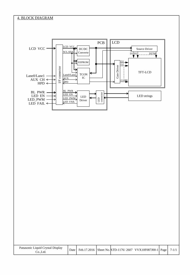
4. BLOCK DIAGRAM
Panasonic Liquid Crystal DisplayCo.,Ltd. Page 7-1/1Date Feb.17.2016 Sheet No.ATD-117612607 VVX10F087J00-1
LCD PCB
TFT-LCD
G1
D1
Lane0/Lane1
G2
D2 D5760
Source Driver
EEPROM
Gat
e D
river
DC/DC Converte
TCON IC
G1080
LED
co
nnec
tor
LCD VCC
LED strings
AUX CH HPD
BL PWR LED EN
LED_PWM
SCL,SDA
Lane0/Lane1
LCD VCC
AUX HPD
BL PWR LED EN LED PWM LED FAIL
LED Driver
LED FAIL
I/F c
onne
ctor

5. INTERFACE PIN ASSIGNMENT5. 1 Pin alignment
Connector's Part Number : HD2S030HA1 (Maker : JAE)
Notes 1) All pins should be connected to the power supply for LCD on the customer's product.2) All pins should be connected to GND(0V) on the customer's product.3) All pins should be connected to the power supply for Backlight on the customer's product.4) H=on (active), L=off (non-active)
5) Keep open. (It is no problem because this pin has an internal pull-up.)
6) H=Nomal state, L=Abnormal state
Lane0_N
8 High Speed Ground (0V) 2)
BL_PWRBL_PWR
SDASCL
6 Complement Signal Link Lane 0
7II
23IO9 AUX_CH_P 24
-True Signal Link Lane 0 Enable signal for Backlight 4)
Brightness control of Backlight 4)LED_PWM ILED_EN I
IO
22Lane0_PH_GND
10
Keep open or connect to GND 29
LCD_VCCLCD_VCC
11 High Speed Ground (0V)
I
122)
No. No.PIN
DESCRIPTION Note
True Signal Link Lane 1
2 High Speed Ground (0V) 2)
3)
I2C-bus Clock
GND (0V)
Power supply for LCD
-H_GNDAUX_CH_N IO
26
30
NoteDESCRIPTION
2)
5)5)
Power supply for Backlight
GND (0V) 2)
GND (0V)
GND (0V)
25
BL_PWRBL_PWR
I2C-bus Data
28
-
IComplemnt Signal Aux Channel
True Signal Aux Channel
13BISTLCD_GND
P
15 2)14
1-O
3 Complement Signal Link Lane 1
Abnormal detection of Backlight
2)5 High Speed Ground (0V)
II4-
Hot plug detection
16 -O
-19
2)
20BL_GND
SYMBOL
LED_FAILH_GNDLane1_NLane1_PH_GND
BL_GND
I/O
LCD_GNDHPD
SYMBOL
18
6)
PIN
17
BL_GNDBL_GND
I/O
21
GND -
P27
1)
VVX10F087J00-1 Page 8-1/3Panasonic Liquid Crystal DisplayCo.,Ltd. Date Feb.17.2016 Sheet No.ATD-117612608
PIN No.30 PIN No.1
Cable

5. 2 Correspondence between input data and display imageDisplay data of adjacent two pixel is latched during four cycle of DCLK(Dot clock).
Pixel : B0 - B7 : B (x,y)B G R G0 - G7 : G (x,y)
(1,1) (1,1) (1,1) R0 - R7 : R (x,y)
- - - - - - - - - - - - - - - - - - - - - - - - - - - -- - - - - - - - - - - - - - - - - - - - - - - - - - - -- - - - - - - - - - - - - - - - - - - - - - - - - - - -
1080 , 2 1080 , 3 1080 , 1920
3 , 1 3 , 2 3 , 3 3 , 1920
Panasonic Liquid Crystal DisplayCo.,Ltd.
2 , 1 2 , 2 2 , 3 2 , 19201 , 1 1 , 2 1 , 3 1 , 1920
1080 , 1
Page 8-2/3Date Feb.17.2016 Sheet No.ATD-117612608 VVX10F087J00-1
Invalid Invalid 1,1 1,2 1,1919 2,1 2,2 1,1920
DCLK
R0-R7 G0-G7 B0-B7
DE
2,3

5. 3 Relationship between display colors and input signals
MSB LSB MSB LSB MSB LSB
Note 1) Definition of gray scale :Color(n)・・・・Number in parenthesis indicates gray scale level.
Larger n corresponds to brighter level.2) Data : 1 : High, 0 : Low
Blue DataR7 R6 R5 R4 G5 G4 B1R1 R0 G7 G6R3 R2
0 0 00Black 0 0 0 0 0 0 0 000 01
0 0 00 0 0 0001 1 0 0 0Red(255) 1 1 1 1
001 1Green(255) 0 0 0 0 0Blue(255) 0 0 0 0
10
0 0 0
Color Cyan 0 0 000 0 0Basic
111 1 1 10 1
0 0Magenta 1 1 1 1 1
11Yellow 1 1 1 1 1 1 1 0 0
White 1 1 1 1 1 1 11 01 1 0 0
1 101 0 01 1 1 1
000 0Black 0 0 0 0 0
0 0 10 0 00 0 0 0
Red (1) 0 0 0 0 0 00 00Red (2) 0 0 0 0 0
00 00 0 0 0 0 0 00 00 1 0 0 0 00 0
0 00 00 0 0 0 0 0
0 0 0 0 0 0 0 0 0:Red : : : : : : : : : : :
1 1
:: : : : :
: :
1 11 1 1 1
: : : :
1 11 1 1 1
: :: : : :: : : : : :: : : :: : : : : : : :: :
0 0 01 1 1 1 1 00
001 1 1 0 0
Red(254)
0 0 0 0 0
1 1 0 0
01Red(255) 1 1 1 1
Green (1) 0 0 0 0Black 0 0 0 0
00 000 00 0 00
0 0 0 00 0 0 00 0
00 00 0 0 0
0 00 0 00 0 0 00 0 0 0 0 10 0
1 1
Green
0 000 0 0 0
1 11 1 0 0 0 0 0 0 1 1 1 1
Green (2) 0 0 0 0 0
: : : :
0 0: : : :
0 0 00 0
:00000 10 0 00 0 0
: :: : :: :
: :: :0 0
: : :: : :
1 1 10 0 0 0 1 1 11 1 1 1
:: : : :0 0 0
0
:: : ::: :
1 0
: : : :Green(254) 0 0 0 0 0
01 1 1
: :0 0 1 1
0 1 1 10 0 0 0
:: :
10 0 1 11 1
0 00 00 00 0 1 1
: :0
0
:1
0 0 0 010 0 0 0 0 1Green(255)
00 00
0 0Black 01 1 1 1
100
0 00
Blue (1) 00 0 0 00 0 0 0
1 1 1 1 1 0 000 0 0
00 0
00
0 0 000 00 0 0 00 0 0 0 0 0
0 001
0 0 0 00 0
0 00 0 0 0
Blue (2) 0
0 000
0 0 0 0
0 0 0 00
0
0 0
00 0 0Blue
0 10 0: :
0 0 0 00: : : :
0
: : : : :: : : : : : : : : : :: : : ::
:: : :
:: : : : :: : : : :: :: :0 1 1Blue (254) 0 0 0 0 0 0 00 0
0 0Blue (255) 0 0 0 0
1 10 0 1 1
0 100 1 11 1 1 1
1 10 0 00 0
00
0 0 0
B5
0
B3 Input
Color
Red Data Green Data
: : ::
B4
0
B2 B0G3 G2 G1 G0 B7 B6
VVX10F087J00-1 Page 8-3/3Panasonic Liquid Crystal DisplayCo.,Ltd. Date Feb.17.2016 Sheet No.ATD-117612608

6. INTERFACE TIMING6. 1 eDP receiver characteristics
(1) DisplayPort Main Link Receiver Characteristics
(2) DisplayPort AUX Channel Characteristics
Note 1) Coupling capacitor is not mounted on our PCB.
mA
us
100 - Ω
2.0 V
1.32
IAUX_SHORT AUX Short circuitcurrent limit
- - 90
-
VAUX_CM AUX DC common modevoltage
0 -
UI AUX Unit interval 0.4 0.5 0.6
Panasonic Liquid Crystal DisplayCo.,Ltd.
RAUX_TERM AUX CH terminationresistance
-
-
Ω
Symbol Description
VAUX_DIFFp-pAUX Differential
peak-to-peak input voltage0.32
-
nF 1)CAUX AUX AC couplingcapacitor - 100
V
For HBR.
ISHORT Short circuit current limit
Min. Typ. Max. Unit
- 100 ps
mA
Comments
LSKEW Lane Intra-pair skew
VCM DC common modevoltage
- - 50
RTERM Differential terminationresistance
- 100 -
0 - 2.0 V
Min. Typ. Max. Unit Comments
120 - 1200 mV For HBR.
Symbol Description
VDIFFp-p Differential peak-to-peakinput voltage
Page 9-1/4Date Feb.17.2016 Sheet No.ATD-117612609 VVX10F087J00-1
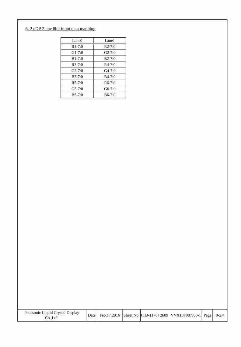
6. 2 eDP 2lane 8bit input data mapping
G5-7:0 G6-7:0B5-7:0 B6-7:0
Panasonic Liquid Crystal DisplayCo.,Ltd.
R5-7:0 R6-7:0
R3-7:0 R4-7:0G3-7:0 G4-7:0B3-7:0 B4-7:0
B1-7:0
Lane0 Lane1R1-7:0 R2-7:0
B2-7:0G1-7:0 G2-7:0
Page 9-2/4Date Feb.17.2016 Sheet No.ATD-117612609 VVX10F087J00-1

6. 3 SYNCRONIZATION SIGNAL TIMING
Frame rate 60Hz
tCLKTBD 2200 TBD tCLK
Horizontal Valid tHD 1920
Vertical Valid tVDDE
Vertical PeriodNOTE
1080 tHtV TBD 1125 TBD tH
UNIT
Horizontal Period tH
ITEM SYMBOL Min. Typ. Max.
VVX10F087J00-1 Page 9-3/4Panasonic Liquid Crystal DisplayCo.,Ltd. Date Feb.17.2016 Sheet No.ATD-117612609
tH tHD
tV tVD
DE
DE
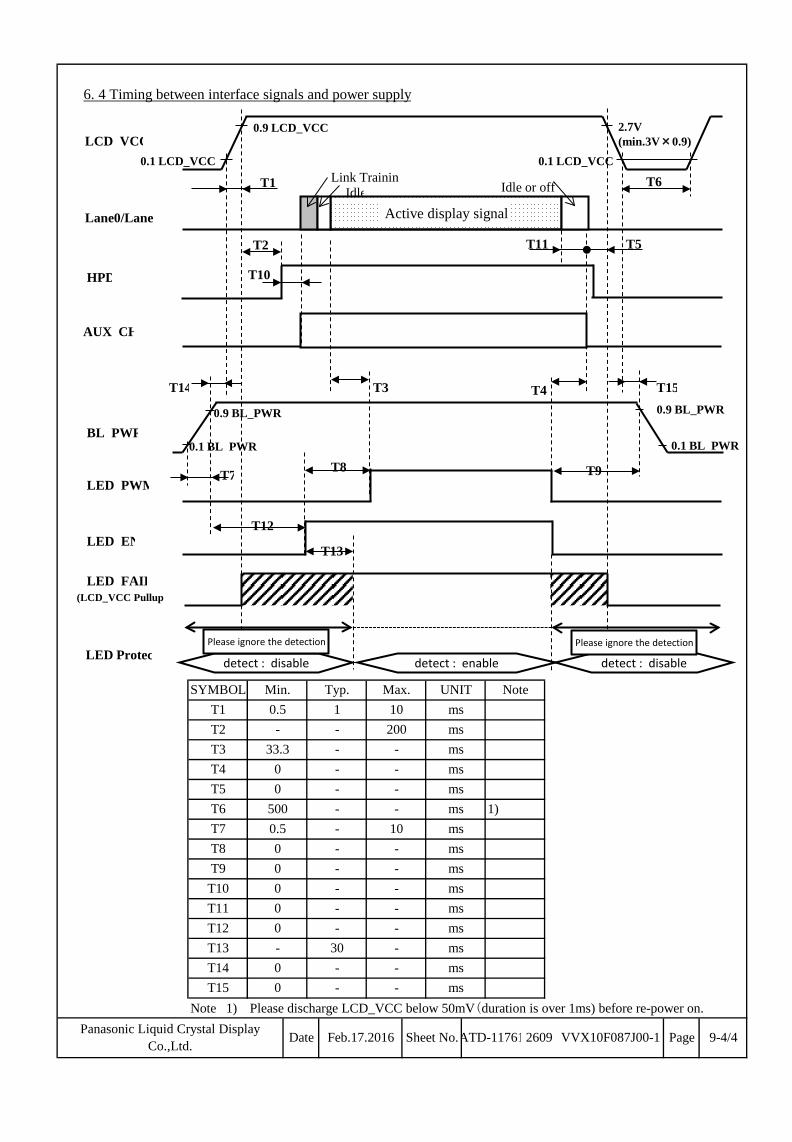
6. 4 Timing between interface signals and power supply
Note 1) Please discharge LCD_VCC below 50mV(duration is over 1ms) before re-power on.
T13 - 30 -
T11 0 -T12 0 -
1)
--
ms
ms
msms
-
--
200 msT2 -
T4 0T3 33.3
0.5
0T6 500
0T8T7
T5
msms
- -
-
- -
-
ms- 10ms-ms
-
-T9 0 -T10 0
ms
VVX10F087J00-1 Page 9-4/4
--
ms
Panasonic Liquid Crystal DisplayCo.,Ltd. Date Feb.17.2016 Sheet No.ATD-117612609
SYMBOL Min. Typ. Max. UNIT NoteT1 0.5 1 10 ms
T14 0 - - msT15 0 - - ms
LCD VCC 2.7V (min.3V×0.9)
0.1 LCD_VCC
T5
T4
Lane0/Lane
LED PWM
LED EN
BL PWR
HPD
T2
T3
T1 T6 Link Training Idle Idle or off
Active display signal
AUX CH
T7
0.9 BL_PWR
0.1 BL PWR
0.9 BL_PWR
0.9 LCD_VCC
0.1 LCD_VCC
T8 T9
T10
0.1 BL PWR
T11
LED FAIL
T12
T13
(LCD_VCC Pullup)
detect : disable detect : disable detect : enable LED Protec
T14 T15
Please ignore the detection Please ignore the detection

7. LABEL FORMAT7.1 Label
The label is on the Backlight Frame as shown in 11. Dimensional outline.The style of character will be changed without notice.
① Contents of ②~⑧ are indicated by bar codes. 【Express by the data matrix】② PLD③ MP : VVX10F087J00 (WS ~ CS : SSX10F087J00)④ Please refer Note 1)⑤ Please refer Note 2)⑦ 4 digits for serial number (0001 - ZZZZ) without I and O and U and V.⑩ Please refer Nore 3)⑥,⑧,⑨ A cord for production of PLD inside management.
Note 1) Note 2) Note 3) 01 , The 1st week of year WS : WS 02 , The 2nd week of year ES : ES
15 2015 03 , The 3rd week of year CS : CS16 2016 04 , The 4th week of year MP : 01 - ZZ17 2017 05 , The 5th week of year
06 , The 6th week of year ・・・・・ 52 , The 52th week of year
10-1/1Page2610 VVX10F087J00-1ATD-11761
Mark Year
Panasonic Liquid Crystal DisplayCo.,Ltd. Date Feb.17.2016 Sheet No.
(10mm)
(12mm) *** **
PLD
①
②
④ ⑤
③
⑩
⑨
⑧
⑦ ⑥
VVX10F087J00
1549G0000

9. PRECAUTIONPlease pay attention to the followings when a TFT module with a backlight unit is used, handled and mounted.
9.1 Precaution to handling and mounting(1) Applying strong force to a part of the module may cause partial deformation of frame or mold, and cause damage to the display.(2) The module should gently and firmly be held by both hands. Never hold by just one hand in order to avoid any internal damage. Never drop or hit the module.(3) Uneven force such as twisted stress should not be applied to a module when a module is mounted on the cover case. The cover case must have sufficient strength so that external force can not be transmitted directly to a module.(4) It is recommended to leave a space between a module and a holding board of a module so that partial force is not applied to a module.(5) A transparent protective plate should be added on the display area of a module in order to protect a polarizer and TFT cell.The transparent protective plate should have sufficient strength so that the plate can not touch a module by external force. (6) Materials included acetic acid and choline should not be used for a cover case as well as other parts and boards near a module. Acetic acid attacks a polarizer. Choline attacks electric circuits due to electro-chemical reaction. (7) The polarizer on a TFT cell should carefully be handled due to its softness, and should not be touched, pushed or rubbed with glass, tweezers or anything harder than HB pencil lead. The surface of a polarizer should not be touched and rubbed with bare hand, greasy clothes or dusty clothes.(8) The surface of a polarizer should be gently wiped with absorbent cotton, chamois or other soft materials slightly contained petroleum benzene when the surface becomes dirty. Normal-hexane or Isopropyl alcohol as cleaning chemicals is recommended in order to clean adhesives which fix front/rear polarizers on a TFT cell. Other cleaning chemicals such as acetone, toluen and alcohol should not be used to clean adhesives because they cause chemical damage to a polarizer. (9) Saliva or water drops should be immediately wiped off. Otherwise, the portion of a polarizer may be deformed and its color may be faded. (10) The module should not be opened or modified. It may cause not to operate properly.(11) A module should not be handled with bare hand or dirty gloves. Otherwise, color of a module fixed sheet and metal frame may become dirty during its storage. It is recommended to use clean soft gloves and clean finger stalls when a module is handled at incoming inspection process and production (assembly) process.(12) Printed circuits board part should not be held and touched. It may cause not to operate properly.
9.2 Precaution to operation(1) The ambient temperature near the operated module should be satisfied with the absolute maximum ratings. Unless it meets the specifications, sufficient cooling system should be adopted to system.(2) The spike noise causes the mis-operation of a module. The level of spike noise should be as follows: -100mV ≦ over- and under- shoot of VDD ≦ +100mV VDD including over- and under- shoot should be satisfied with the absolute maximum ratings. (3) Optical response time, luminance and chromaticity depend on the temperature of a TFT module. (4) Sudden temperature change may cause dew on and/or in the a module. Dew makes damage to a polarizer and/or electrical contacting portion. Dew causes fading of displayed quality.(5) Fixed patterns displayed on a module for a long time may cause after-image. It will be recovered soon.(6) A module has high frequency circuits. Sufficient suppression to electromagnetic interference should be done by system manufacturers. Grounding and shielding methods may be effective to minimize the interference. (7) Noise may be heard when a backlight is operated. If necessary, sufficient suppression should be done by system manufacturers.
Panasonic Liquid Crystal DisplayCo.,Ltd. Page 12-1/3Date Feb.17.2016 Sheet No.ATD-117612612 VVX10F087J00-1

(8) The module should not be connected or removed while a main system works.(9) Inserting or pulling I/F connectors causes any trouble when power supply and signal data are on-state. I/F connectors should be inserted and pulled after power supply and signal data are turned off.(10)Do not keep the LCD panel with its operation in the condition while the backlight is turned off
because there is a possibility that the panel is charged up and may cause MURA.
9.3 Electrostatic discharge control(1) Since a module consists of a TFT cell and electronic circuits with CMOS-ICs, which are very weak to electrostatic discharge, persons who are handling a module should be grounded through adequate methods such as a list band. I/F connector pins should not be touched directly with bare hands.(2) Protection film for a polarizer on a module should be slowly peeled off so that the electrostatic charge can be minimized.
9.4 Precaution to strong light exposure(1) A module should not be exposed under strong light. Otherwise, characteristics of a polarizer and color filter in a module may be degraded.
9.5 Precaution to storageWhen modules for replacement are stored for a long time, following precautions should be taken care of:(1) Modules should be stored in a dark place. It is prohibited to apply sunlight or fluorescent light during storage. Modules should be stored at 0 to 35℃ at normal humidity (60%RH or less).(2) The surface of polarizers should not come in contact with any other object. It is recommended that modules should be stored in the Panasonic Liquid Crystal Display's shipping box.
9.6 Precaution to handling protection film(1) The protection film for polarizers should be peeled off slowly and carefully by persons who are electrically grounded with adequate methods such as a list band. Besides, ionized air should be blown over during peeling action. Dusts on a polarizer should be blown off by an ionized nitrogen gun and so on. (2) The protection film should be peeling off without rubbing it to the polarizer. Because, if the film is rubbed together with the polarizer, since the film is attached to the polarizer with a small amount of adhesive, the adhesive may remain on a polarizer.(3) The module with protection film should be stored on the conditions explained in 10.5 (1). However, in case that the storage time is too long, adhesive may remain on a polarizer even after a protection film is peeled off. Besides, in case that a module is stored at higher temperature and/or higher humidity, adhesive may remain on a polarizer. The remained adhesive may cause non-uniformity of display image.(4) The adhesive can be removed easily with Normal-Hexane or Isopropyl alcohol. The remained adhesive or its vestige on the polarizer should be wiped off with absorbent cotton or other soft materials such as chamois slightly contained Normal-Hexane or Isopropyl alcohol.(5) The procedure of peeling protection film on polarizer is recommended as follows. Peel off protection film from upper polarizer film with tape. Please peel off the protection film like the below figure.
Panasonic Liquid Crystal DisplayCo.,Ltd. Page 12-2/3Date Feb.17.2016 Sheet No.ATD-117612612 VVX10F087J00-1
Pull tab
Gate IC side
LED side

9.7 Safety(1) Since a TFT cell is made of glass, handling to the broken module should be taken care sufficiently in order not to be injured. Hands touched liquid crystal from a broken cell should be washed sufficiently.(2) The module should not be taken apart during operation so that backlight drives by high voltage.
9.8 Environmental protectionFlexible printed circuits and printed circuits board used in a module contain small amount of lead. Please followlocal ordinance or regulations for its disposal.
9.9 Use restrictions and limitations(1) This product is not authorized for use in life support devices or systems, military applications or other applications which pose a significant risk of personal injury.(2) In no event shall Panasonic Liquid Crystal Display Co.,Ltd., be liable for any incidental, indirect or consequential damages in connection with the installation or use of this product, even if informed of the possibility thereof in advance. These limitations apply to all causes of action in the aggregate, including without limitation breach of contact, breach of warranty, negligence, strict liability, misrepresentation and other torts.
9.10 OthersElectrical components which may not affect electrical performance are subjective to change without notice because of their availability.
Panasonic Liquid Crystal DisplayCo.,Ltd. Page 12-3/3Date Feb.17.2016 Sheet No.ATD-117612612 VVX10F087J00-1

10. PACKING10.1 Precaution to handling and mounting
1) Standard packing specification
Package information
(*) without product weight
13-1/2Sheet No.
1296
ATD-11761Date
ITEMS
-
Feb.17.2016
Pallet524 × 339 × 214
(inner size)
Packing weight [kg] (*)
Product quantity[Pieces] 36
Box
Panasonic Liquid Crystal DisplayCo.,Ltd.
1100 × 1100 × 1560
VVX10F087J00-1 Page
130
Size [mm]
2613
Module (Back side)
Module (Screen side)
PE bag(module)
Tray
※1 Put the 2 modules in 1 groove ※2 Screen on the inside
Desiccant
Heat seal
Tape
Carton Box
Cushion B
Cushion A
Cushion A
Tape
Carton Label
PE bag (Tray)
Tray cover
Corner Angle A
Packing Strap
Pallet
Corner Angle B
Stretch Film
(1100)
(1100)
Insertion side of the forklift. The traveling direction of the truck.

10.2 Label sample of packing box
VVX10F087J00YY-MM-DD-* REV.** ***
********* VVX10F087J00 000**
********* DDA********* 000****
Serial No. is defined as follows.1 7 B 0001
Date (Refer to the table 1.)The production base refers to Note (1) Base Code mentioned above. Month (Refer to the table 2.)Year (Last 1digit of AD)
Table 1 Date ※Do not use I.O.1 2 3 4 5 6 7 8 9 10 11 121 2 3 4 5 6 7 8 9 A B C
13 14 15 16 17 18 19 20 21 22 23 24D E F G H J K L M N P Q25 26 27 28 29 30 31R S T U V W X
Table 2 Month ※Do not use I.O.1 2 3 4 5 6 7 8 9 10 11 12A B C D E F G H J K L M
Panasonic Liquid Crystal DisplayCo.,Ltd.
(d) This shows product name.(e) Lot of registration(f) Revision (Rev.)(g) PLD internal code.(h)
Date Feb.17.2016 Sheet No.ATD-117612613 VVX10F087J00-1 Page 13-2/2
Code Contents of Printing(a) PLD internal code.(b) The place of issuing label.(c) Quantity of the product (pcs)
Serial No. of identification tag
11 Serial No. (0001~9999 and A000~Z999) mustbe continuous. Do not reset.
DateCodeDateCodeDateCode
MonthCode
(j) Bar code corresponds to (h).(k) Bar codes correspond to (h), (a),(c) and (f).(n) Bar codes correspond to (d), (c).(p) Panasonic Liquid Crystal Display Co., Ltd.
production ship (ex.) (102mm)
(70m
m)
DDA********** **pcs
Panasonic Liquid crystal Display Co.,Ltd. ** ( a)
( d)
( b)
( c)
( e) ( g)
( j ) ( n)
( h)
( k)
( h) ( a) ( c)
( f )
( d) ( c)
( f )
( p)

Page
No.
Date 14 - 1/2Panasonic Liquid Crystal Display Co., Ltd. ATD-11761 2614 VVX10F087J00
Sheet
Sep.18.2015
11. Dimensional outline
<Front View>
NOTES:UNLESS OTHERWISE SPECIFIED.1) () INDICATES REFERENCE DIMENSION.2) THICKNESS MEASURING FORCE IS 7N~9N.
CL
PULLTAB
13
8.0
5 ±
0.4
0[O
UTL
INE]
12
3.9
3 ±
0.1
0[A
CTI
VE A
REA
]
220.32 ±0.10[ACTIVE AREA]
4.5
0 ±
0.5
0[A
A -
> O
UTL
INE]
232.70 ±0.40[OUTLINE]
5.12 ±0.50[AA -> OUTLINE]
224.32 ±0.30[POL.]
(2)[AA -> POL.]
12
7.9
3 ±
0.3
0[P
OL.
]
(2
)[A
A -
> P
OL.
]

147.78 ±1[CENTER OF I/F CONNECTOR ->OUTLINE]
14 - 2/2Panasonic Liquid Crystal Display Co., Ltd. ATD-11761 2614 VVX10F087J00 Page
Sheet
No.
Date Sep.18.2015
BL LABEL
CL
LCM LABEL PULLTAB
10
9.7
7 ±
1[I
/F C
ON
NEC
TOR
->
OU
TLIN
E]
(3
4.4
1)
6 max.[W/ PCB]
4.13 ±0.25[W/O PCB]
<Back View>
NOTES:UNLESS OTHERWISE SPECIFIED.1) () INDICATES REFERENCE DIMENSION.2) THICKNESS MEASURING FORCE IS 7N~9N.

Our company network supports you worldwide with offices in Germany, Great Britain, Turkey and the USA.
For more information please contact:
Distec GmbH
Augsburger Str. 2b
82110 Germering
Germany
Phone: +49 (0)89 / 89 43 63-0
Fax: +49 (0)89 / 89 43 63-131
E-Mail: [email protected]
Internet: www.datadisplay-group.de
FORTEC Elektronik AG
Lechwiesenstr. 9
86899 Landsberg am Lech
Germany
Phone: +49 (0)8191 / 911 72-0
Fax: +49 (0)8191 / 217 70
E-Mail: [email protected]
Internet: www.fortecag.de
Display Technology Ltd.
5 The Oaks Business Village
Revenge Road, Lordswood
Chatham, Kent, ME5 8LF
United Kingdom
Phone: +44 (0)1634 / 67 27 55
Fax: +44 (0)1634 / 67 27 54
E-Mail: [email protected]
Internet: www.datadisplay-group.com
Apollo Display Technologies, Corp.
87 Raynor Avenue,
Unit 1Ronkonkoma,
NY 11779
United States of America
Phone: +1 631 / 580-43 60
Fax: +1 631 / 580-43 70
E-Mail: [email protected]
Internet: www.apollodisplays.com
Sales Partner:
DATA DISPLAY BİLİŞİM TEKNOLOJİLERİ
İÇ VE DIŞ TİCARET LİMİTED ŞİRKETİ
Barbaros Mh. Ak Zambak Sk. A Blok D:143
34376 Ataşehir / Istanbul
Turkey
Phone: +90 (0)216 / 688 04 68
Fax: +90 (0)216 / 688 04 69
E-Mail: [email protected]
Internet: www.data-display.com.tr


![Panasonic Crs1 Mechanism[1]](https://static.fdocuments.in/doc/165x107/5525e781550346fc6e8b4a92/panasonic-crs1-mechanism1.jpg)


![Panasonic 9th Generation Plasma Display Repair Training Manual[ET]](https://static.fdocuments.in/doc/165x107/55259533550346446f8b491a/panasonic-9th-generation-plasma-display-repair-training-manualet.jpg)


