
Data Synchronizer Performance in the Presence of Parameter ...
111
Data Synchronizer Performance in the Presence of Parameter Variability by Samuel K. Dunham, Bachelor of Science A Thesis Submitted in Partial Fulfillment of the Requirements for the Degree of Master of Science in the field of Electrical Engineering Advisory Committee: Dr. George Engel, Chair Dr. Bradley Noble Dr. Robert Leander Graduate School Southern Illinois University Edwardsville August, 2014
Transcript of Data Synchronizer Performance in the Presence of Parameter ...

Data Synchronizer Performance in the Presence of Parameter Variability
by Samuel K. Dunham, Bachelor of Science
A Thesis Submitted in PartialFulfillment of the Requirements
for the Degree ofMaster of Science
in the field of Electrical Engineering
Advisory Committee:
Dr. George Engel, Chair
Dr. Bradley Noble
Dr. Robert Leander
Graduate SchoolSouthern Illinois University Edwardsville
August, 2014

c© Copyright by Samuel K. Dunham August, 2014All rights reserved

ABSTRACT
DATA SYNCHRONIZER PERFORMANCE IN THE PRESENCE OF PARAMETERVARIABILITY
by
SAMUEL K. DUNHAM
Chairperson: Professor George Engel
In digital integrated circuit design, synchronization of data across clock domains is
an issue that has proven difficult for engineers over the years. It is not uncommon for
SoC (System on Chip) designs to contain thousands of data synchronizers. The risk of
metastability is becoming greater due to shrinking feature size. Designs that enter the
deep sub-micron realm are much more prone to serious performance degradation as a result
of variation in process, voltage, and temperature (PVT). As a result, metastability-related
failures are likely to increase in the future. It is therefore more important than ever before
that engineers responsible for the design of safety-critical circuits understand the impact
of variability on the performance of synchronizers used throughout their design.
In order to spotlight the growing importance of reliable data synchronization in modern
designs, this thesis describes the design of a synchronizer cell which is to be made publicly
available so that engineers interested in the subject may have access to a concrete circuit
which can be used for investigations of metastability-related issues. A design methodology
which uses AC analysis to optimize the GBW (Gain-Bandwidth) product of the inverter
cascade in the critical regenerative loops is described, and an equation relating GBW to
the characteristic metastability resolution time constant, τ , is derived.
ii

Formal sensitivity theory is used to address the issue of how PVT variability affects
performance. The thesis goes on to demonstrate how the results obtained through
simulation (or through actual measurements on silicon) at one operating point may be
used, in an iterative manner, to predict synchronizer performance over a wide range of
operating temperatures and supply voltages. Simulating the performance at a single
operating point can take minutes or even hours, and measurements on actual silicon can
take hours or days so the approach presented here can save reliability engineers valuable
time. The design of a second circuit, designed specifically to be used as a dedicated
synchronizer cell, is also presented. The use of a radically different topology is intended
to demonstrate the robustness of our approach to predicting changes in performance in
the presence of parameter variability.
The results from the sensitivity analysis is compared to simulation. The quality
of the model’s fit to the actual data is quantified using two metrics: the coefficient of
determination, R2, and the RMS error of the deviation between the predicted and actual
data values. For both designs under consideration, when the supply voltage was swept
from 0.8 V to 1.2 V, R2 exceeded 0.97 and the RMS error in the worst case was 2.6 ps
(with a typical value of 0.5 ps). For the case of changing temperature (over the entire
automotive range), R2 exceeded 0.99 and the RMS error in the worst case was 0.7 ps.
iii

ACKNOWLEDGEMENTS
I would like to thank Dr. George L. Engel who has supported me in my education
from undergraduate and beyond. He has been able to see the true potential in me as a
student and engineer, as well as bring it out. I would also like to thank Dr. Brad Noble,
who has provided me with support inside and outside of classes. Additional thanks goes
to Dr. Scott Smith and Dr. Andy Lozowski who have helped to lay the foundations
of my knowledge and allow me to explore different facets of electrical engineering in a
non-traditional manner.
I would like to thank the National Science Foundation (NSF) for providing money
to support this research. This work is carried out under NSF STTR Phase II-B Grant
#0924010 “Blended Clocked and Clockless Integrated Circuit Systems”. I would like to
thank personally Dave Zar, Jerry Cox, and the rest of the Blendics team for providing
insight and support throughout this research endeavor.
I extend my gratitude towards Jacob Hostettler and Marica Fesler as well, who have
been with me for almost the entirety of my college education. Lastly, I extend my thanks
to my parents, grandmother, and my brother who have supported me throughout my life.
Without their help and support I would never have become the person I am.
iv

TABLE OF CONTENTS
ABSTRACT . . . . . . . . . . . . . . . . . . . . . . . . . . . . . . . . . . . . . . ii
ACKNOWLEDGEMENTS . . . . . . . . . . . . . . . . . . . . . . . . . . . . . . iv
LIST OF FIGURES . . . . . . . . . . . . . . . . . . . . . . . . . . . . . . . . . . vii
LIST OF TABLES . . . . . . . . . . . . . . . . . . . . . . . . . . . . . . . . . . . ix
Chapter
1. INTRODUCTION . . . . . . . . . . . . . . . . . . . . . . . . . . . . . . 1
1.1 Role of Data Synchronizers in Modern Computer Systems . . . . . . 11.2 Metastability Hazards . . . . . . . . . . . . . . . . . . . . . . . . . . 51.3 Estimating Mean Time Between Failure (MTBF) Rates . . . . . . . 71.4 Impact of Technology Scaling on Synchronizer Performance . . . . . 101.5 Need for Public Domain Synchronizer Cells . . . . . . . . . . . . . . 121.6 MetaACE: A Tool for the Study of Synchronizer Performance . . . . 131.7 Object and Scope of Thesis . . . . . . . . . . . . . . . . . . . . . . . 14
2. IMPACT OF VARIATION IN PROCESS, VOLTAGE, ANDTEMPERATURE ON METASTABILITY PARAMETERS . . . . . . . 16
2.1 Characterization of Metastability . . . . . . . . . . . . . . . . . . . . 172.2 Modeling a Metastable Flip-Flop . . . . . . . . . . . . . . . . . . . . 182.3 FET I-V Characteristics . . . . . . . . . . . . . . . . . . . . . . . . . 212.4 Device Characterization . . . . . . . . . . . . . . . . . . . . . . . . . 242.5 Expressions for Characteristic Time Constant . . . . . . . . . . . . . 272.6 Formal Sensitivity Analysis . . . . . . . . . . . . . . . . . . . . . . . 292.7 Sensitivity of τ to Supply Voltage . . . . . . . . . . . . . . . . . . . 312.8 Sensitivity of τ to Threshold Voltage . . . . . . . . . . . . . . . . . . 332.9 Sensitivity of τ to Temperature . . . . . . . . . . . . . . . . . . . . . 352.10 Predicting Trends Given Single Known Value of τ . . . . . . . . . . 372.11 PVT Tolerant Design . . . . . . . . . . . . . . . . . . . . . . . . . . 38
3. DESIGN AND CHARACTERIZATION OF A STANDARDFLIP-FLOP USED AS A SYNCHRONIZER . . . . . . . . . . . . . . . 40
3.1 Design Objectives . . . . . . . . . . . . . . . . . . . . . . . . . . . . 403.2 Optimization of Gain Bandwidth Product of Inverter Loops . . . . . 433.3 Transistor Sizing . . . . . . . . . . . . . . . . . . . . . . . . . . . . . 453.4 Physical Layout . . . . . . . . . . . . . . . . . . . . . . . . . . . . . 51
v

3.5 Design Verification . . . . . . . . . . . . . . . . . . . . . . . . . . . . 533.6 Dependence of τ on Supply Voltage . . . . . . . . . . . . . . . . . . 553.7 Dependence of τ on Threshold Voltage . . . . . . . . . . . . . . . . . 623.8 Dependence of τ on Temperature . . . . . . . . . . . . . . . . . . . . 63
4. DESIGN AND CHARACTERIZATION OF A SPECIALIZEDSYNCHRONIZER CELL . . . . . . . . . . . . . . . . . . . . . . . . . . 68
4.1 Design Objectives and Overview . . . . . . . . . . . . . . . . . . . . 684.2 Optimization of Gain Bandwidth Product of Inverter Loops . . . . . 724.3 Transistor Sizing . . . . . . . . . . . . . . . . . . . . . . . . . . . . . 734.4 Physical Layout . . . . . . . . . . . . . . . . . . . . . . . . . . . . . 764.5 Design Verification . . . . . . . . . . . . . . . . . . . . . . . . . . . . 774.6 Modifications to Sensitivity Analysis for the Specialized
Synchronizer Circuit . . . . . . . . . . . . . . . . . . . . . . . . . . 784.7 Dependence of τ on Supply Voltage . . . . . . . . . . . . . . . . . . 814.8 Variability of the Metastability Voltage . . . . . . . . . . . . . . . . 834.9 Dependence of τ on Temperature . . . . . . . . . . . . . . . . . . . . 84
5. SUMMARY, CONCLUSIONS, AND FUTURE WORK . . . . . . . . . . 86
5.1 Sensitivity Analysis . . . . . . . . . . . . . . . . . . . . . . . . . . . 865.2 A Standard Flip-Flop Synchronizer Case Study . . . . . . . . . . . . 875.3 A Specialized Synchronizer Case Study . . . . . . . . . . . . . . . . 885.4 Future Work . . . . . . . . . . . . . . . . . . . . . . . . . . . . . . . 89
REFERENCES . . . . . . . . . . . . . . . . . . . . . . . . . . . . . . . . . . . . . 91
APPENDIX . . . . . . . . . . . . . . . . . . . . . . . . . . . . . . . . . . . . . . . 93
vi

LIST OF FIGURES
Figure Page
1.1 An Example of a Synchronous Circuit and Its Operation . . . . . . . . . 21.2 Mechanical Metastability . . . . . . . . . . . . . . . . . . . . . . . . . . . 31.3 A Traditional D-latch Illustrating The Propagation Delay Around The Loop 61.4 ITRS technology road map . . . . . . . . . . . . . . . . . . . . . . . . . 111.5 MetaACE Showing a Circuit Exiting Metastability . . . . . . . . . . . . 14
2.1 Cross-Coupled Inverters . . . . . . . . . . . . . . . . . . . . . . . . . . . 182.2 Small-Signal Equivalent Circuit . . . . . . . . . . . . . . . . . . . . . . . 192.3 Testbench Used To Characterize FETs in The 45 nm Process . . . . . . 252.4 Regression Analysis Results for Low Threshold Devices . . . . . . . . . . 262.5 Regression Analysis Results for General-Purpose Threshold Devices . . . 262.6 Regression Analysis Results for High Threshold Devices . . . . . . . . . . 26
3.1 A Multiplexer-Based Latch . . . . . . . . . . . . . . . . . . . . . . . . . 413.2 LSSD Master Slave D Flip-Flop . . . . . . . . . . . . . . . . . . . . . . . 423.3 Linearly Cascaded Amplifiers . . . . . . . . . . . . . . . . . . . . . . . . 433.4 Small Signal Testbench for The Master Loop . . . . . . . . . . . . . . . . 463.5 Small Signal Testbench for The Slave Loop . . . . . . . . . . . . . . . . . 483.6 GBW as a Function of Device Width for The Master Loop . . . . . . . . 493.7 GBW as a Function of Device Width for The Slave Loop . . . . . . . . . 503.8 Physical Layout for a LSSD Master-Slave D Flip-Flop . . . . . . . . . . . 523.9 Predicted vs. Simulated τ for VTL Master Loop Devices . . . . . . . . . 583.10 Predicted vs. Simulated τ for VTL Slave Loop Devices . . . . . . . . . . 583.11 Predicted vs. Simulated τ for VTG Master Loop Devices . . . . . . . . . 603.12 Predicted vs. Simulated τ for VTG Design with VTL Loop Devices . . . 623.13 Predicted VTG τ vs. Simulated VTG τ . . . . . . . . . . . . . . . . . . 633.14 Predicted vs. Simulated τ for VTL Master Loop Devices in the
Automotive Temperature Range . . . . . . . . . . . . . . . . . . . . . 643.15 Predicted vs. Simulated τ for VTL Slave Loop Devices in the
Automotive Temperature Range . . . . . . . . . . . . . . . . . . . . . 653.16 Predicted vs. Simulated τ for VTG Master Loop Devices in the
Automotive Temperature Range . . . . . . . . . . . . . . . . . . . . . 663.17 Predicted vs. Simulated τ for VTG with VTL Master Loop Devices
in the Automotive Temperature Range . . . . . . . . . . . . . . . . . 66
4.1 A Pseudo-NMOS Latch Schematic . . . . . . . . . . . . . . . . . . . . . 694.2 A Pseudo-NMOS Flip-Flop Schematic . . . . . . . . . . . . . . . . . . . 714.3 Small Signal Testbench for Both Master and Slave Loops . . . . . . . . . 744.4 GBW vs. NFET Width for Different PFET Lengths . . . . . . . . . . . 754.5 GBW vs. NFET Width for Different Non-Ideal Wiring Capacitances . . 764.6 Physical Layout for a Differential NMOS Flip-Flop . . . . . . . . . . . . 77
vii

4.7 Common Source Amplifier with a Resistive Load . . . . . . . . . . . . . 804.8 Predicted vs. Simulated τ for VTL Slave Loop . . . . . . . . . . . . . . 834.9 Vm vs. VDD Comparison Between Chapter 3 and Chapter 4 Circuits . . 844.10 Predicted vs. Simulated τ for VTL Slave Loop in the Automotive
Temperature Range . . . . . . . . . . . . . . . . . . . . . . . . . . . . 85
viii
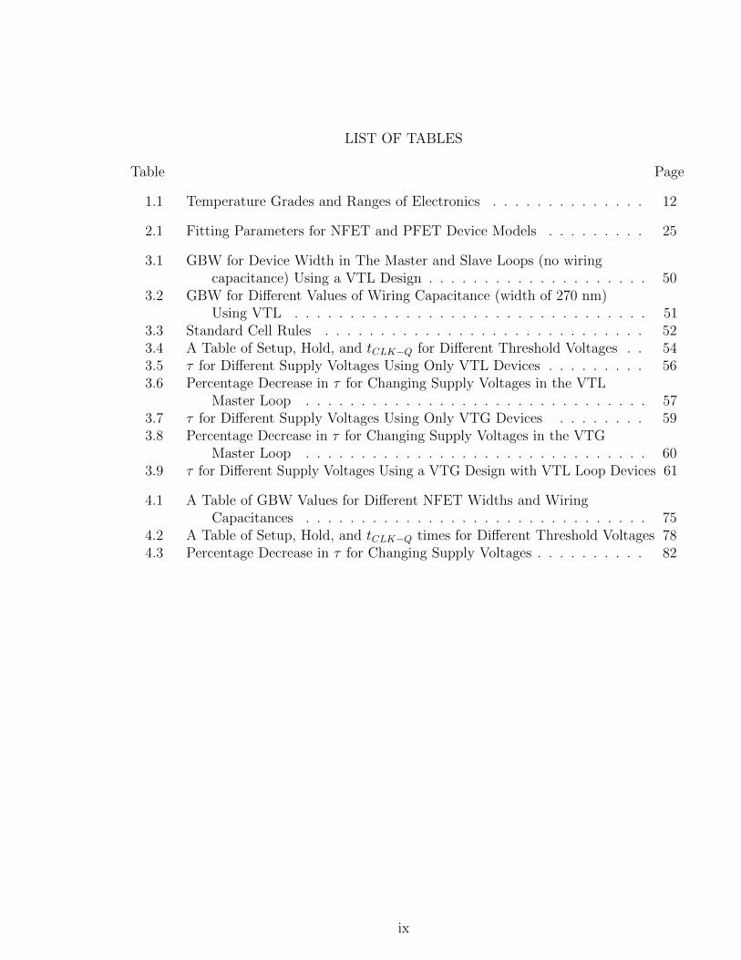
LIST OF TABLES
Table Page
1.1 Temperature Grades and Ranges of Electronics . . . . . . . . . . . . . . 12
2.1 Fitting Parameters for NFET and PFET Device Models . . . . . . . . . 25
3.1 GBW for Device Width in The Master and Slave Loops (no wiringcapacitance) Using a VTL Design . . . . . . . . . . . . . . . . . . . . 50
3.2 GBW for Different Values of Wiring Capacitance (width of 270 nm)Using VTL . . . . . . . . . . . . . . . . . . . . . . . . . . . . . . . . 51
3.3 Standard Cell Rules . . . . . . . . . . . . . . . . . . . . . . . . . . . . . 523.4 A Table of Setup, Hold, and tCLK−Q for Different Threshold Voltages . . 543.5 τ for Different Supply Voltages Using Only VTL Devices . . . . . . . . . 563.6 Percentage Decrease in τ for Changing Supply Voltages in the VTL
Master Loop . . . . . . . . . . . . . . . . . . . . . . . . . . . . . . . 573.7 τ for Different Supply Voltages Using Only VTG Devices . . . . . . . . 593.8 Percentage Decrease in τ for Changing Supply Voltages in the VTG
Master Loop . . . . . . . . . . . . . . . . . . . . . . . . . . . . . . . 603.9 τ for Different Supply Voltages Using a VTG Design with VTL Loop Devices 61
4.1 A Table of GBW Values for Different NFET Widths and WiringCapacitances . . . . . . . . . . . . . . . . . . . . . . . . . . . . . . . 75
4.2 A Table of Setup, Hold, and tCLK−Q times for Different Threshold Voltages 784.3 Percentage Decrease in τ for Changing Supply Voltages . . . . . . . . . . 82
ix

CHAPTER 1
INTRODUCTION
1.1 Role of Data Synchronizers in Modern Computer Systems
In the modern world of computing, the days in which an integrated circuit (IC)
with multiple clock domains being an oddity are gone. Multiprocessor and Network on
Chip (NoC) designs are becoming more prolific in devices which people use every day.
With the proliferation of designs which have multiple clock domains, synchronization of
information across domains is a more pressing challenge. Although the issues associated
with synchronization have been known for many years, engineers still do not understand
metastability well and how to handle the problem properly. Before continuing our
discussion of metastability, an overview of synchronous circuitry will be covered.
Sequential circuitry is present in almost every digital design and has been for years.
It is necessary because it introduces the notion of state. While combinational circuitry
is only concerned with present values, sequential circuitry is concerned with past and
present values. This implies the system has memory [Katz, 2005].
Sequential design has two fundamental styles: asynchronous and synchronous. Syn-
chronous design will be used for the work in this thesis. In a synchronous design a clock
signal is used to tell all of the memory elements when to update, while combinational
logic is used to determine how the states should update. These types of systems are
referred to as state machines.
One important aspect of synchronous design is that the combinational logic must not
change value when states are updated [Katz, 2005]. A block diagram of a synchronous
system and scenarios of correct and incorrect operation are seen in Figure 1.1. When
data transitions during the clock transition, metastability can result.
Metastability in digital circuits is a phenomenon that occurs when data being clocked

2
Figure 1.1: An Example of a Synchronous Circuit and Its Operation

3
in transitions before the value is registered. If this type of transition presents itself,
the circuit will enter a state that is undefined. In digital logic, there are two defined
stable states, “1” and “0”. These values are designated by logic level voltages. Designers
typically use ground and the supply voltage to represent“0” and “1” respectively.
The issue of metastability can be given an analogous situation in mechanical terms.
A very popular analogy used in literature is that of a ball on a hill. In Figure 1.2 it is
seen that there are two troughs and a hill. If the ball is in either of the troughs, it is in a
stable position. If the ball is located on top of the hill it will remain there until some
outside force, such as wind, knocks it into one of the troughs. Theoretically the ball will
remain on the hill until some outside force knocks it off into one of the troughs. Much in
the same way, a circuit in metastability can remain at an undefined voltage until it is
influenced by some other voltage. In reality, a circuit will not likely remain metastable
for a long period of time, but even one clock cycle can cause catastrophe [Li, 2011].
Figure 1.2: Mechanical Metastability
One might be inclined to ask why is this so problematic? Noise will help kick the
circuit out of this state. The problem is that other sequential logic will typically rely on
this value. If two or more different state machines take this value There is a chance that
they will each interpret this value differently. Now the question is why should a designer
be concerned if for one cycle, the circuits misinterpret the input? The reason for concern

4
is that the system may enter a state that the designer never intended. If this state is
entered, there may be no way to exit it without reset. Since this is far from ideal, is there
a way to avoid metastability all together?
Unfortunately, this phenomenon is an unavoidable consequence of the nature of
sequential logic. If a clock domain crossing (CDC) is necessary, it will always pose a
threat. Even in the absence of a CDC, if unexpected clock skew is introduced between
registers, metastability may result. Although an engineer cannot eliminate the threat of
metastability, good design practices can at least mitigate the threat. The solution to this
problem is a special circuit called a synchronizer.
Traditionally, a synchronizer was used to capture information that was presented
asynchronously to a system [Ginosar, 2011]. While this is still a problem in which a
synchronizer is employed, it is now just as common to see it used in any situation where
metastability poses an immediate threat. This could be seen in two-clock FIFOs (First-in
First-out) or in multicore systems where clocks may be mesochronous or multisynchronous
[Ginosar, 2011].
The job a synchronizer must perform might seem simple, but is exceedingly complex.
The goal is to transfer information reliably from a system being clocked at one frequency
to another system clocked at a different frequency. The problem comes in that the designer
has no guarantee that data will fall within the valid sampling window. The role of the
synchronizer in this scenario is to reduce the probability of a metastable event to as small
of a number as possible or to resolve metastability as fast as possible.
Until recently, metastability has been a very difficult issue to document. Several
reasons contribute to this problem. Firstly, one must have this rare event happen. Some
researchers have influenced the conditions with the use of data flip-flops and proper
experimental conditions [Chaney and Molnar, 1973]. While this provides insight into
metastability as a phenomenon, it does not adequately demonstrate the different scenarios
5
in an IC where this problem arises. Designers still have trouble observing this issue outside
of the lab setting. Researchers have found success in using Infrared Emission analysis
(IREM) to determine if synchronizers are entering metastability [Beer et al., 2013]. The
chip observed by researchers was experiencing an abnormally large amount of failures that
were theorized to be caused by metastability. IREM allowed the researchers to observe
“hot spots” in key locations on the chip. These corresponded to metastable synchronizers.
To verify this theory, the researchers used focused ion beam (FIB) micro-probes to see
that there was a short pulse at the output of a synchronizer which is coincident with
metastability. This behavior was predicted according to their earlier work.
It is because of recent advances in metastability detection, as described above, that
the topic of metastability is getting greater attention. In order to reduce the chances of
metastability-related failure, engineers must be adequately equipped to cope with this
situation. The next section will cover different hazards associated with metastability in a
synchronizer circuit in more depth.
1.2 Metastability Hazards
Previously, the idea of a critical time period was mentioned in regards to metastability.
This critical time period is an inherent property of the latching mechanism of any sequential
circuit. Latching is the action in a circuit when a value presented at the input is held,
indefinitely, assuming the usage of static sequential logic. A latch has two operating
modes. The first is transparent, in which it allows data to pass through as if it were a
wire. The second is hold, in which the data is held constant until the next sampling edge
of the clock. When a circuit latches, there are two timing constraints which must be
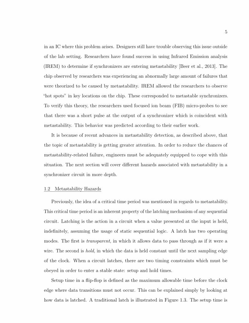
obeyed in order to enter a stable state: setup and hold times.
Setup time in a flip-flop is defined as the maximum allowable time before the clock
edge where data transitions must not occur. This can be explained simply by looking at
how data is latched. A traditional latch is illustrated in Figure 1.3. The setup time is

6
Figure 1.3: A Traditional D-latch Illustrating The Propagation Delay Around The Loop
seen as the amount of time it takes for the signal to propagate fully around the loop so
that a stable value is set [Weste, 2006].
Hold time is the amount of time after a clock edge in which the data must not
transition. The reasoning for this is that the switches which close the latch, transitioning
from transparency to latched, have a non-zero propagation delay due to the potential
overlap of clock signals. Overlap of signals can be caused by devices not switching fast
enough [Weste, 2006].
There are three types of metastability hazards which designers must contend with:
• Uncertainty in transition timing
• Uncertainty in logic level
• Data-skew uncertainty
Should a synchronizer become metastable, there can be a one cycle uncertainty in the
transition at the receiving domain. In this event, the uncertainty occurs according to
whether the source transitions before or after a critical data-clock-offset at the destination.
If the transition is precisely at the critical data-clock-offset, a separatrix forms between
the higher and lower family of metastability settling traces. If infinitely precise timing of

7
the offset positioning was possible, unbounded settling time would be observed. This is
referred to as uncertainty in timing [Cox, 2014].
Uncertainty in logic level is a problem when the result of a synchronizer is delivered
to multiple destination registers. If the output of a synchronizer is metastable when a
destination device samples its output, then the destination devices may interpret this
value differently. In the event of logic level uncertainty, there is the possibility that the
system will enter an unintentional state [Cox, 2014].
A third hazard which can be coincident with, but not caused by, metastability is
data-skew uncertainty. This hazard occurs at CDCs when data transitions arriving from
a source are skewed. When these bits are skewed, some may change before the clock
edge and some after. This hazard can occur regardless of whether the source domain is
metastable. It is only of concern if the timing skew between domains is sufficient enough
that setup or hold times are violated [Cox, 2014].
1.3 Estimating Mean Time Between Failure (MTBF) Rates
While metastability is unavoidable, one can mitigate the chance of an occurrence to
a great degree. If designed properly, the probability of a metastable event can be made
longer than the life cycle of any given product. This section will investigate the details of
predicting the Mean Time Between Failure (MTBF) of a given synchronizer. First, a few
parameters must be defined.
The simplest synchronous system will have a clock signal and data signal, each with
a given period TC and TD. There is no reason that the frequency of the data and the
frequency of the clock have to be the same, and hence they both must be specified in order
to get an accurate value of MTBF. A time window , TW , is defined about the sampling
edge of the clock signal [Ginosar, 2011]. This window defines the time period in which a
data transition can lead to metastability.
When the coincidence of clock and data is unknown, probability must be used in order
8
to assess the likelihood of a failure. The simplest and preferred model assumes that data
changes occur with a uniform distribution. If data is known to change during a given clock
cycle, the probability of a failure is known and given by Equation (1.1) [Ginosar, 2011].
Failure Probability =TCTW
(1.1)
D may not change every cycle, so a modification must be made to Equation (1.1).
Taking the period with which D actively changes (TD) into account, the failure rate is
calculated as
Failure Rate for a given data rate =TCTDTW
=1
fCfDTW(1.2)
While this predicts the chance of entering metastability, it is also necessary to consider
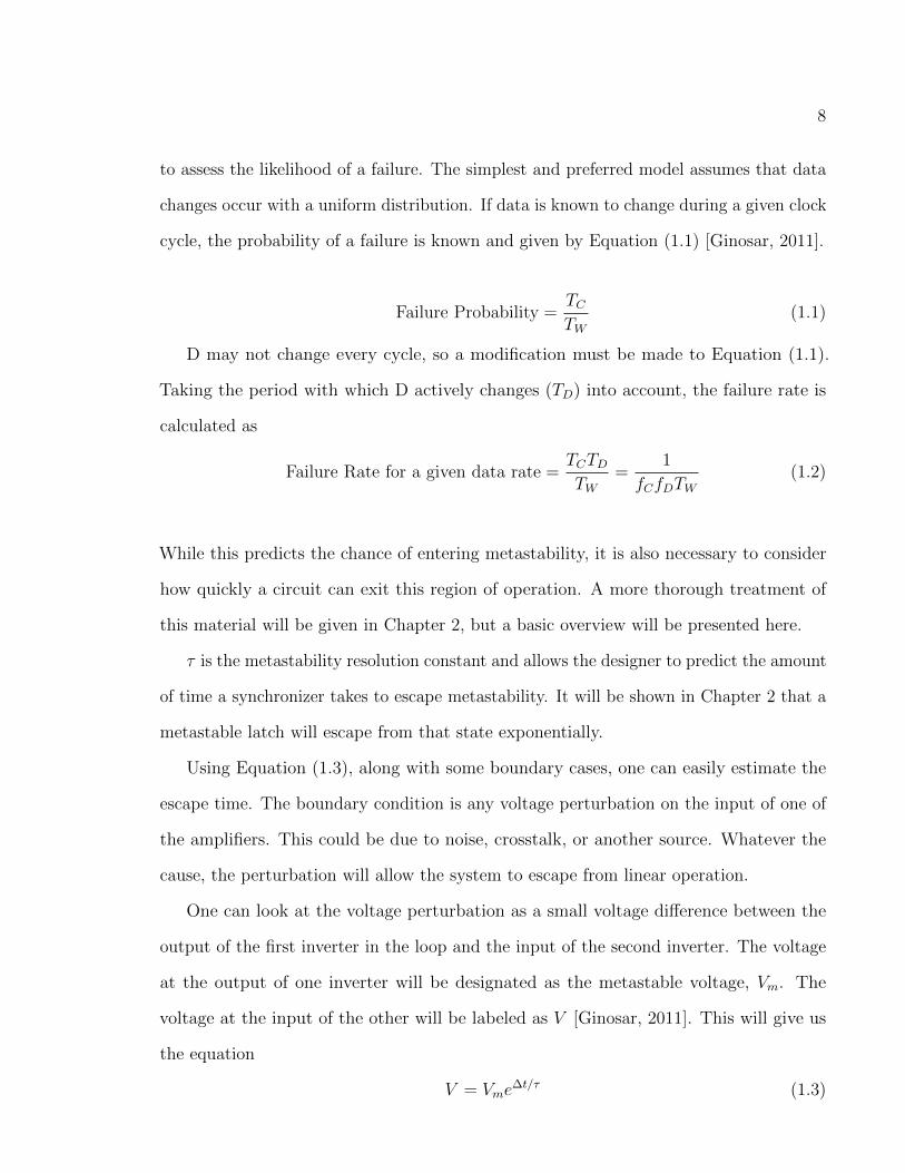
how quickly a circuit can exit this region of operation. A more thorough treatment of
this material will be given in Chapter 2, but a basic overview will be presented here.
τ is the metastability resolution constant and allows the designer to predict the amount
of time a synchronizer takes to escape metastability. It will be shown in Chapter 2 that a
metastable latch will escape from that state exponentially.
Using Equation (1.3), along with some boundary cases, one can easily estimate the
escape time. The boundary condition is any voltage perturbation on the input of one of
the amplifiers. This could be due to noise, crosstalk, or another source. Whatever the
cause, the perturbation will allow the system to escape from linear operation.
One can look at the voltage perturbation as a small voltage difference between the
output of the first inverter in the loop and the input of the second inverter. The voltage
at the output of one inverter will be designated as the metastable voltage, Vm. The
voltage at the input of the other will be labeled as V [Ginosar, 2011]. This will give us
the equation
V = Vme∆t/τ (1.3)
9
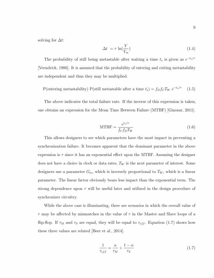
solving for ∆t:
∆t = τ ln(V
Vm) (1.4)
The probability of still being metastable after waiting a time ts is given as e−ts/τ
[Veendrick, 1980]. It is assumed that the probability of entering and exiting metastability
are independent and thus they may be multiplied.
P(entering metastability) P(still metastable after a time ts) = fDfCTW e−ts/τ (1.5)
The above indicates the total failure rate. If the inverse of this expression is taken,
one obtains an expression for the Mean Time Between Failure (MTBF) [Ginosar, 2011].
MTBF =ets/τ
fCfDTW(1.6)
This allows designers to see which parameters have the most impact in preventing a
synchronization failure. It becomes apparent that the dominant parameter in the above
expression is τ since it has an exponential effect upon the MTBF. Assuming the designer
does not have a choice in clock or data rates, TW is the next parameter of interest. Some
designers use a parameter Gtv, which is inversely proportional to TW , which is a linear
parameter. The linear factor obviously bears less impact than the exponential term. The
strong dependence upon τ will be useful later and utilized in the design procedure of
synchronizer circuitry.
While the above case is illuminating, there are scenarios in which the overall value of
τ may be affected by mismatches in the value of τ in the Master and Slave loops of a
flip-flop. If τM and τS are equal, they will be equal to τeff . Equation (1.7) shows how
these three values are related [Beer et al., 2014].
1
τeff=
α
τM+
1− ατS
(1.7)
10
where
τeff is the effective settling time constant
τM is the settling time constant for the Master latch
τS is the settling time constant for the Slave latch
α is the duty cycle, usually around 0.5
This changes the MTBF equation to
MTBF =ets/τeff
fCfDTW(1.8)
When the Master and Slave settling time constants differ, α makes a significant impact
on τeff . While alpha must be within the vicinity of 0.5 to avoid violation of minimum
clock pulse width, it may vary somewhat. For especially large differences in τM and τS, α
must be considered since τeff is in the exponent [Beer et al., 2014].
1.4 Impact of Technology Scaling on Synchronizer Performance
Modern Systems on Chip (SoC) have grown increasingly complex over the decades,
and with this increase in complexity comes new challenges for designers. Moore’s Law,
which states that the number of transistors that can be fit on a die doubles approximately
every two years, has been a major contributing factor to the increase in design complexity.
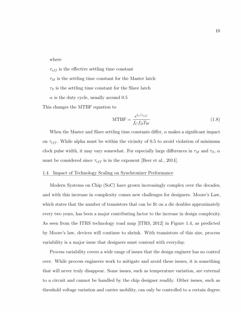
As seen from the ITRS technology road map [ITRS, 2012] in Figure 1.4, as predicted
by Moore’s law, devices will continue to shrink. With transistors of this size, process
variability is a major issue that designers must contend with everyday.
Process variability covers a wide range of issues that the design engineer has no control
over. While process engineers work to mitigate and avoid these issues, it is something
that will never truly disappear. Some issues, such as temperature variation, are external
to a circuit and cannot be handled by the chip designer readily. Other issues, such as
threshold voltage variation and carrier mobility, can only be controlled to a certain degree.
11
Figure 1.4: ITRS technology road map
There are two types of process variations that significantly impact designers. The first
type is inter-die, which is the variation over several chips, or lot by lot. These affect how
well chips from different production runs perform and must be known in order to produce
a consistent product. The second type is intra-die which is the variation between devices
on a single chip. These are important because variation within the design can lead to
different failure modes in designs [Saonwani et al., 2012].
Saonwani and others have shown that threshold voltage can have a 6σ standard
deviation of ±10% in designs using 90 nm down to 32 nm technology. They have
also shown that the effective length and oxide thickness can vary by ±12% and ±4%
respectively. Through Monte-Carlo analysis, they showed that these parameter variations
can lead up to a 25% variation in gate delays of simple gates. The gates analyzed in
the paper were static CMOS combinational logic gates (NAND and NOR) but are still
applicable to general design [Saonwani et al., 2012].
In any electronics technology an important variable is the operating temperature of the
device or devices in use. Companies have designated temperature ranges for devices to aid
engineers in selecting parts. The engineers in IC design must especially take temperature
into account since other engineers will be using these circuits for a myriad of applications.

12
Altera defines the standards in Table 1.1 for the temperature grades of their electronics
[Altera, 2014]. Looking at the table, it is obvious that the temperature ranges are so large
that variation of metastability parameters due to this phenomenon should be accounted
for by designers.
Temperature Grade Temperature Range
Commercial 0◦C to 85◦C
Industrial -40◦C to 100◦C
Military -55◦C to 125◦C
Automotive -40◦C to 125◦C
Table 1.1: Temperature Grades and Ranges of Electronics
With variations in delays in logic, it is difficult to design a fast sequential circuit that
will be unlikely to violate setup and hold times. It is clear that with such large variations
in gate delays, routing will become increasingly important at smaller technology nodes.
Overall, between temperature variations and process variability, the need for a robust
synchronizer is growing. It is thus important that designers be able to predict trends in
metastability parameters based upon PVT variability.
1.5 Need for Public Domain Synchronizer Cells
Many researchers and designers do not have the time to devote to the development of
synchronizer standard cells. Rather than specially designed custom cells, a designer will be
tempted to use standard data flip-flops. This can lead to poor design if not done properly.
This section will discuss the main motivations for design of the public synchronizer cells
developed in this thesis.
Many practicing designers and their managers do not have a good understanding of
metastability and its hazards. The increase of parameter variability due to shrinking de-

13
vices compounds the risks of synchronization failure. Techniques designers used previously
do not hold well in the worst case scenarios, and even small variation poses a risk.
In current designs, there is a greater emphasis on design reliability. This means that
engineers will need a way to make accurate estimates on MTBF. With a public domain
synchronizer, designers will have a readily available design to aid them in understanding
the pitfalls they are likely to encounter in estimating metastability-related MTBF rates.
1.6 MetaACE: A Tool for the Study of Synchronizer Performance
Most simulators are not well suited for the analysis and behavior prediction of
metastable circuitry. Designers and test engineers in general take the approach of writing
scripts and testbenches. Unfortunately, in writing testbenches, it is easy to neglect details
necessary to accurately model metastability. MetaACE is designed with these types of
issues in mind.
Since this thesis involves the extensive study of synchronizer circuitry, it requires
a great deal of analysis to make accurate predictions. Rather than writing extensive
and overly complex testbenches, MetaACE will be used to verify numerical predictions.
MetaACE is the first commercial product for simulation and analysis of synchronizer
failure. This software also has the unique property of giving predictions of circuit behavior
across process corner, voltage, and temperature variations.
MetaACE is able to output data in a simple “.csv” file for use in other software. In
the files it produces, an engineer can find the value of τ , TW , the metastable voltage, and
other parameters of interest. It also allows parametric sweeps of temperature and voltage.
The GUI shows the user the family of separatrix curves formed when exiting metastability
as seen in Figure 1.5.
Throughout this thesis, MetaACE will provide data for comparison against empirical
data and analytically predicted data. It will serve as a baseline for the accuracy of the
methods developed and used throughout this work.

14
Figure 1.5: MetaACE Showing a Circuit Exiting Metastability
1.7 Object and Scope of Thesis
As mentioned in earlier sections in this chapter, metastability is a very dangerous
condition for systems with asynchronous inputs or multiple clock domains. The purpose of
the work done for this thesis is to develop techniques for the design of robust synchronizers.
Aside from developing a systematic design procedure for synchronizers, a mathematical
model is presented which accounts for the effects of process, voltage, and temperature
variations. These two topics will allow designers to accurately predict the MTBF of
a given synchronizer circuit, and the variation in this value one can expect in a given
process.
The second chapter of the thesis will explore PVT variability and its effects on
metastability parameters. A model of a flip-flop when metastable will be discussed in
detail. Afterword, the I-V characteristics of the devices used in the circuits discussed in
this thesis will be explored in a detailed manner. This will then be applied to develop
analytic expressions for the metastability resolution time constant in the strong and weak
inversion regions. A short introduction to formal sensitivity analysis will be given. This
will be used to derive sensitivity functions for the variation of the metastability resolution

15
time constant, τ in the presence of process, temperature, and voltage (PVT) variation.
A method by which the results can be used in an interative manner will be presented.
The iterative technique allows one to predict variations in τ over wide ranges in supply
voltage and/or operating temperature. Finally, PVT design tolerance will be discussed
briefly before continuing on to apply the techniques in the later chapters of this thesis.
The third chapter will explore a simple data flip-flop modified for use as a synchronizer.
The design objectives will be clearly stated, as well as an explanation of the reasons for
the design chosen. Afterword, an explanation of the importance of the gain-bandwidth
product (GBW) in the inverter loops and its relation to τ will be derived. An empirical
method for properly sizing these devices will be explained as well as the results of this
technique. The details of the physical layout process and decisions are considered due to
the effects of wiring capacitance on τ . Design verification will be used to show the benefits
and issues with the given topology. Finally, the dependence of τ upon supply voltage,
threshold, and temperature are discussed comparing MetaACE results to the sensitivity
equations developed in Chapter 2. These equations will be applied to designs using
low-threshold and generaly-purpose threshold devices. The final sections of this chapter
will verify the accuracy of the sensitivity analysis both qualitatively and quantitavely.
The fourth chapter is similar to the third chapter, but a different topology will be
used to show the benefits one can achieve when using non-traditional flip-flop designs.
This will also serve to show the robustness of the techniques discussed in Chapter 2. This
chapter will not present as many comparisons as Chapter 3, but instead show that the
general predictions in trends still hold true. An exhaustive comparison will be left as
future work.
The final chapter will give a summary of the thesis, conclusions drawn, and the future
work intended.
16
CHAPTER 2
IMPACT OF VARIATION IN PROCESS, VOLTAGE, AND TEMPERATURE ON
METASTABILITY PARAMETERS
The goal of this chapter is to investigate the impact of variation in process, voltage, and
temperature (PVT) on the performance of a data synchronizer. As the size of the devices
integrated on a chip shrink, the effects of variability become more significant. As explained
in Chapter 1, it is becoming more important than ever before to fully understand how
PVT variability influences performance since this has a direct bearing on the overall
reliability of an electronic system.
Chapter 2 begins by discussing two parameters (τ and TW ) which characterize the
metastable behavior of a flip-flop. The chapter goes on to explain how the the regenerative
loops in a flip-flop should be modeled so that these parameters may be determined. This
is followed by a discussion of the I-V characteristics of Field-Effect Transistors (FETs) for
both the strong and weak inversion regimes. The various devices available to a designer
in the 45 nm target process are then characterized, and expressions for the metastability
resolution time constant are derived. This is followed by a short introduction to formal
sensitivity analysis. The chapter concludes by deriving a set of equations which describe
the sensitivity properties of the resolution time constant, τ , with respect to changes in
supply voltage, threshold voltage, and temperature.
The sensitivity properties derived in this chapter will be used in Chapters 3 and 4 to
demonstrate that given a single known value of τ , its value at other operating temperatures
or supply voltages can be predicted with surprising accuracy. The significance of this fact
is that if a value of τ is determined, for example, experimentally (a very time consuming
endeavor) or through simulation (also time demanding) at one temperature and supply
voltage, the equations derived in this chapter can then predict with a reasonable degree
17
of accuracy the values of τ at other temperatures and supply voltages without the need
to make any additional measurements. This can result in a huge savings in time for the
reliability engineer who is interested in knowing the performance of the synchronizer over
a wide range of operating conditions.
2.1 Characterization of Metastability
It is well-known that the delay properties of a flip-flop when in a metastable state are
exponential in nature and depend upon two parameters:
• Metastable characteristic time constant, τ ,
• Metastable time aperture window, TW .
These parameters can be extracted from simulation and then used to model the delay
behavior of a flip-flop when metastable, but the determination of these parameters is
not easy and must be be undertaken with great care. For this reason a commercial tool,
MetaACE, is used to simulate the performance of two competing synchronizer designs.
These two synchronizer designs will be discussed at length in Chapters 3 and 4 of this
thesis. This goal of the chapter is to outline steps designers should follow to produce
circuits which are PVT tolerant and then to validate these claims using the synchronizer
designs presented in succeeding chapters.
A common metric used to quantify a flip-flops’s metastable behavior is the metastability
window. This window is defined by Equation (2.1),
δ = TW e−tsτ (2.1)
where TW is the asymptotic width of the window with no settling time, and τ is the
characteristic resolution time constant associated with the feedback loop in the flip-flop.
18
One may think of TW as the normalized time aperture when metastability may occur.
The characteristic time constant, τ , is to be interpreted as being related to how long the
metastable state will persist if the flip-flop should ever go metastable. In general, the
metastability window, δ, can be defined as the time period where data transitions cannot
be resolved within a specified settling time, ts. Since δ is exponentially dependent upon
τ , a small change in τ can cause a dramatic change in δ [Li, 2011].
Since the impact of variation in τ upon performance is much more significant than
that of TW , this chapter will attempt to investigate the impact that variability in PVT
will have on τ and not on how these variations effect TW . However, the same formal
techniques used to investigate the sensitivity properties of τ could be applied to better
understand how PVT variation affect TW .
2.2 Modeling a Metastable Flip-Flop
Irrespective of the specific circuit topology used to implement a flip-flop, the re-
generative loop, whose performance directly impacts τ , can generally be modeled by a
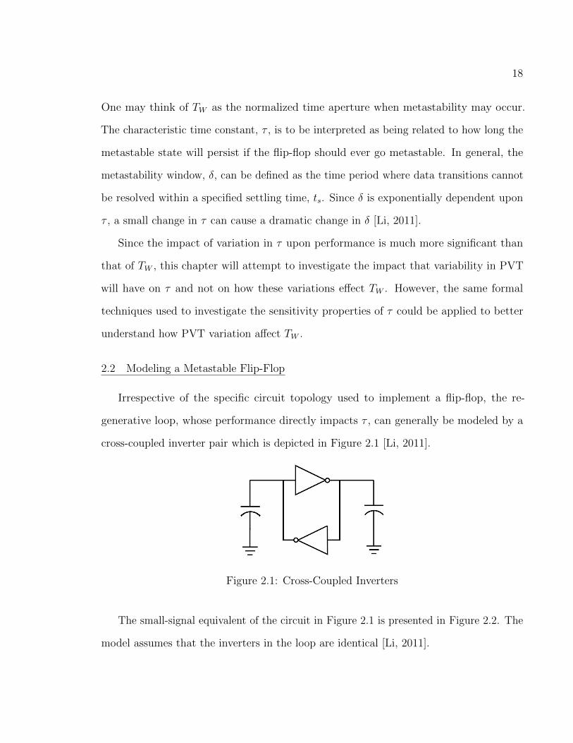
cross-coupled inverter pair which is depicted in Figure 2.1 [Li, 2011].
Figure 2.1: Cross-Coupled Inverters
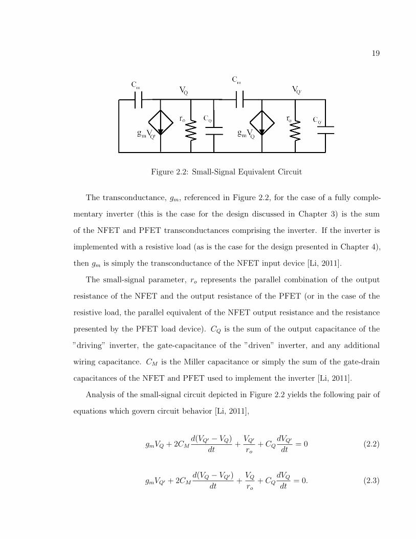
The small-signal equivalent of the circuit in Figure 2.1 is presented in Figure 2.2. The
model assumes that the inverters in the loop are identical [Li, 2011].
19
Figure 2.2: Small-Signal Equivalent Circuit
The transconductance, gm, referenced in Figure 2.2, for the case of a fully comple-
mentary inverter (this is the case for the design discussed in Chapter 3) is the sum
of the NFET and PFET transconductances comprising the inverter. If the inverter is
implemented with a resistive load (as is the case for the design presented in Chapter 4),
then gm is simply the transconductance of the NFET input device [Li, 2011].
The small-signal parameter, ro represents the parallel combination of the output
resistance of the NFET and the output resistance of the PFET (or in the case of the
resistive load, the parallel equivalent of the NFET output resistance and the resistance
presented by the PFET load device). CQ is the sum of the output capacitance of the
”driving” inverter, the gate-capacitance of the ”driven” inverter, and any additional
wiring capacitance. CM is the Miller capacitance or simply the sum of the gate-drain
capacitances of the NFET and PFET used to implement the inverter [Li, 2011].
Analysis of the small-signal circuit depicted in Figure 2.2 yields the following pair of
equations which govern circuit behavior [Li, 2011],
gmVQ + 2CMd(VQ′ − VQ)
dt+VQ′
ro+ CQ
dVQ′
dt= 0 (2.2)
gmVQ′ + 2CMd(VQ − VQ′)
dt+VQro
+ CQdVQdt
= 0. (2.3)

20
If the solution of VQ and VQ′ is assumed exponential, then the voltage observed at the
output, Q, is given by the expression
VQ = VQ(t = 0)etτ = Vme
tτ (2.4)
where Vm is frequently referred to as the ”metastable voltage”. The characteristic
resolution time constant, τ , can be shown to be
τ =CQ + 4CMgm − 1
ro
≈ CLgm
(2.5)
where CL is total capacitance associated with the output node and includes both wiring
capacitance and Miller capacitance. If gmro � 1, where gmro is the low-frequency small-
signal circuit gain of a single inverter, then the approximation in Equation (2.5) is valid
[Li, 2011]. For the designs presented in Chapters 3 and 4, the low-frequency gain of the
inverters in the loop is greater than ten.
From Equation (2.5), it is clear that the sensitivity properties of τ depend upon the
sensitivity properties of gm when the capacitive load, CL, is assumed to be invariant
with respect to changes in threshold voltage, supply voltage, and temperature. This is
generally a reasonable assumption [Li, 2011].
The remainder of the chapter will assume “symmetric” NFETs and PFETs . In other
words, the analysis will assume that the PFET is made somewhat wider to compensate for
its lower mobility, thereby matching it to the NFET. Moreover, the analysis will assume
that the magnitude of the PFET and NFET threshold voltages are approximately the
same. While this ”symmetry” assumption is not absolutely necessary, it simplifies the
analysis and is a good assumption for the designs investigated in this thesis.

21
2.3 FET I-V Characteristics
The first step towards allowing one to predict variation in the metastability character-
istic time constant resulting from PVT variability is to select device models for the N-
and P-type transistors which are sufficiently accurate, yet simple enough so that they can
be used to analytically determine the sensitivity properties of τ .
When a flip-flop is metastable, the devices in the critical cross-coupled inverter loops
can be in one of three operating regions:
• Strong Inversion
• Moderate Inversion
• Weak Inversion
When a transistor is strongly inverted, the gate-source voltage exceeds the threshold
voltage of the device by roughly 200 mV. Current flows between the drain and source
terminals of the device as a result of the applied electric field between those nodes (i.e.
the current is a result of carriers in a conductive channel moving in response to an applied
electric field) [Tsividis, 2011].
However, when weakly inverted the gate-source voltage is approximately equal to or
somewhat less than the threshold voltage. In this mode, current between the drain and
source terminals flows as a result of diffusion, much like what occurs in a Bipolar Junction
Transistor (BJT) where carriers move as result of a gradient in carrier concentration
[Tsividis, 2011]. Since the physics responsible for the flow of current in the two operating
modes is significantly different, it is not surprising that the sensitivity properties of τ will
differ greatly depending upon the operating region of the FETs.
As the analysis shall demonstrate, weakly inverted FETs are much more sensitive to
PVT variation and should therefore be avoided whenever possible. Moderate inversion, as
its name implies, is when gate-source voltage is slightly greater than the threshold voltage,
22
and both diffusion and drift currents are significant. This regime is difficult to model (and
to treat analytically) and will not be addressed further in this thesis. This is unfortunate
since, for example, if the supply voltage is swept over a fairly wide range, the FETs in the
critical loops will likely operate in two or more of the regions described above. While this
work will obtain sensitivity results for both weakly and strongly inverted FETs, there is
no easy way to unify the results [Tsividis, 2011].
When the metastable voltage (approximately half the supply voltage) is a few tenths
of a Volt or more above the threshold voltage, the devices will operate in strong inversion.
The I-V characteristic for a strongly inverted NFET, valid for submicron sized devices, is
given by Equation (2.6) [Razavi, 2001],
iDS =α(vGS − VTH)2
1 + β(vGS − VTH). (2.6)
The coefficients α and β can be used as fitting parameters. These parameters are also
related to physical device parameters in the following manner:
α =1
2nµ0Cox(
W
L) (2.7)
β =µ0
2vsatL+ θ (2.8)
where
µ0 is the low-field surface mobility of the carriers in the channel
n is the sub-threshold slope factor (≈ 1.5)
Cox is the gate oxide capacitance per unit area
W is the width of the device

23
L is the length of the device
VGS is the gate-source voltage
VTH is the threshold voltage
vsat is the saturation velocity of the carriers in the channel
and θ is the mobility degradation coefficient
If β(vGS − VTH) is assumed � 1, the I-V characteristic of Equation (2.6) reduces to
iDS = α(vGS − VTH)2 (2.9)
which is the familiar square-law characteristic for FETs.
This simpler characteristic may be used in the absence of high electric fields. The
expression for β in Equation (2.8) consists of two terms. The first term accounts for
velocity saturation effects. It is well-known that the plot of average carrier velocity in
the channel (on the y-axis) versus applied lateral electric field strength (on the x-axis)
is a straight line whose slope is the low-field surface mobility parameter, µ0. At some
critical electrical field strength, the curve folds over and the carrier velocity reaches its
saturated value, vsat. When the carriers in the channel attain their maximum velocity, the
drain-to-source current ceases to increase. In other words, the high electric field strength
in the lateral direction limits the maximum current which can flow from drain-to-source
[Tsividis, 2011].
Similarly, a large electric field in the vertical direction (between gate and channel) pin
the electrons in the channel near the silicon/silicon-dioxide interface. This ”crowding”
effect lowers mobility and is accounted for by the second term in Equation (2.8) (i.e. by
the mobility degradation coefficient, θ) [Tsividis, 2011]. As will be demonstrated, these

24
high-electric field corrections to the classical equation tend to make τ less sensitive to
PVT variation.
As supply voltage is reduced, the devices in a metastable flip-flop are likely to enter
the moderate or weak inversion regime. The I-V characteristic for a weakly inverted
NFET is modeled by Equation (2.10) [Tsividis, 2011],
iDS = (n− 1)µ0Cox
(W
L
)UT
2evGS−VTH
nUT (2.10)
where UT is the thermal voltage (kTq
).
While weak inversion operation is to be avoided, the sensitivity properties of a weakly
inverted FET can be used to provide an upper bound on the sensitivity functions which
are derived for a strongly inverted FET.
2.4 Device Characterization
The 45 nm, purposely non-manufacturable, technology which is used in this thesis
offers a would-be designer both NFET and PFET devices with three different threshold
voltages:
• Low threshold devices (VTL)
• General-purpose threshold devices (VTG)
• High threshold devices (VTH)
The testbench, illustrated in Figure 2.3, was used to characterize both NFETs and
PFETs for each of three threshold voltages (VTL, VTG, VTH). The length of both NFET
and PFET devices was 50 nm while the width of the NFET was 270 nm and the PFET
width was 405 nm (near optimal widths as determined in Chapter 3 of this thesis). The
reason 50 nm is used instead of 45 nm is the minimum drawn length rules imposed by
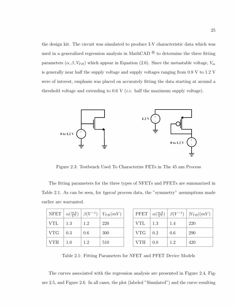
25
the design kit. The circuit was simulated to produce I-V characteristic data which was
used in a generalized regression analysis in MathCAD R© to determine the three fitting
parameters (α, β, VTH) which appear in Equation (2.6). Since the metastable voltage, Vm
is generally near half the supply voltage and supply voltages ranging from 0.8 V to 1.2 V
were of interest, emphasis was placed on accurately fitting the data starting at around a
threshold voltage and extending to 0.6 V (i.e. half the maximum supply voltage).
Figure 2.3: Testbench Used To Characterize FETs in The 45 nm Process
The fitting parameters for the three types of NFETs and PFETs are summarized in
Table 2.1. As can be seen, for typical process data, the ”symmetry” assumptions made
earlier are warranted.
NFET α(mAV 2 ) β(V −1) VTH(mV )
VTL 1.3 1.2 220
VTG 0.3 0.6 300
VTH 1.0 1.2 510
PFET α(mAV 2 ) β(V −1) |VTH |(mV )
VTL 1.3 1.4 220
VTG 0.2 0.6 290
VTH 0.8 1.2 420
Table 2.1: Fitting Parameters for NFET and PFET Device Models
The curves associated with the regression analysis are presented in Figure 2.4, Fig-
ure 2.5, and Figure 2.6. In all cases, the plot (labeled ”Simulated”) and the curve resulting

26
Figure 2.4: Regression Analysis Results for Low Threshold Devices
Figure 2.5: Regression Analysis Results for General-Purpose Threshold Devices
Figure 2.6: Regression Analysis Results for High Threshold Devices

27
from using Equation (2.6) (labeled ”High-field Corrections”) lie on top of one another.
The curve resulting from use of the classical equation (Equation (2.9)) in most cases is a
reasonable fit to the data over the range of gate-source voltages of interest to us (up to 0.6
V), given the fact that τ is proportional to the slope of the curve and that the differences
in slope between the curves predicted by the classical equation and those predicted by
the equation which include high-field effects are relatively small. It is obvious that the
high-field effects are much more important for the VTL devices and not very important
for the VTG and VTH devices. Moreover, one can conclude that use of the classical
equation with the VTL devices will produce overly optimistic values of τ , especially when
the synchronizer is used at elevated supply voltage (> 1.0 V). These observations will
form a guide to when high-field effects should be included in the analysis and when they
can be safely neglected.
2.5 Expressions for Characteristic Time Constant
In the remainder of this chapter, the goal will be to derive equations that predict how
τ will change in response to changes in threshold voltage, supply voltage, and temperature.
Therefore, this section will derive expressions for τ for both strongly inverted and weakly
inverted FETs using the I-V characteristic equations described and validated in earlier
sections of this thesis.
The analysis will begin by deriving an expression for gm using Equation (2.6). The
small-signal transconductance parameter, gm can be computed by taking the partial
derivative of the drain-to-source current with respect to the gate-source voltage,
gm =∂iDS∂vGS
=α(vGS − VTH) [2 + β(vGS − VTH)]
[1 + β(vGS − VTH)]2(2.11)
Therefore, τ for a strongly inverted FET becomes

28
τSI =[1 + β(VM − VTH)]2CL
α(Vm − VTH) [2 + β(VM − VTH)](2.12)
where the metastable voltage (Vm) replaces the gate-source voltage of the NFET. If
high-field effects are neglected (i.e. β(Vm − VTH)� 1), then the expression for τ reduces
to
τSI ≈CL
2α(VM − VTH). (2.13)
On the other hand, for β(Vm − VTH)� 1, τ tends toward a constant,
τSI ≈βCLα
(2.14)
and the conclusion one draws is that high-field effects reduce the variability of τ .
The small-signal transconductance for a weakly inverted FET is given by the expression,
gm =∂iDS∂vGS
=iDSnUT
. (2.15)
Therefore, the expression for τ for a weakly inverted FET when Vm is substituted for
vGS becomes
τWI =nCLe
−(Vm−VTH)nUT
µCox(n− 1)(WL
)UT
. (2.16)
The exponential dependence on the metastable voltage, Vm, and on the threshold
voltage, VTH , suggests that τ will vary greatly when the transistors in the metastable
flip-flop enter weak inversion.

29
2.6 Formal Sensitivity Analysis
It is important that a designer be aware of the effect on circuit performance resulting
from variability in the parameters which govern the behavior of the circuit under design.
In the case of linear, time-invariant circuits a quantifiable measure of this effect can be
expressed in terms of the sensitivity function. A study of circuit sensitivity provides a
designer with insights into circuit behavior when parameters vary. Knowledge of circuit
sensitivity can also be used to evaluate competing designs [Iordache et al., 2008].
The values of circuit parameters may vary for many reasons including:
• Process variability
• Varying supply voltage
• Changing die temperature
• Aging of devices.
Any effect on circuit performance caused by a change in one or more circuit parameters
is referred to as a circuit sensitivity. The relative sensitivity or simply the sensitivity
of a circuit function, f , with respect to a circuit parameter x is defined formally in
Equation (2.17) [Iordache et al., 2008].
Sfx =x
f
∂f
∂x(2.17)
While Equation (2.17) is the form which is most useful when one wishes to compute
the sensitivity function, the equation can be re-written so as to reveal the significance of
the sensitivity factor. According to Equation (2.18), one may interpret the sensitivity
as the ratio of the relative change in the circuit function f to the relative change in
the parameter x, provided the change is ”small” (i.e. approaching zero in the limit)
[Iordache et al., 2008].
30
Sfx =
(∂ff
)(∂xx
) (2.18)
The equation can be re-written in yet a third way,
Sfx =∂lnf
∂lnx. (2.19)
One observes from Equation (2.19)that scaling a function by a constant does not
change the sensitivity properties of the function since ln(kf) = ln(k) + ln(f). This
property of sensitivity analysis is exploited frequently in the derivations presented in the
next three sections of the thesis.
Once a sensitivity function is known, a relative change in a circuit function, f , given
a relative change in a parameter x can be computed using Equation (2.20),
∆f
f= Sfx
∆x
x. (2.20)
When f is a function of multiple variables, then the relative change in the function f
is computed using
∆F
F=
n∑i=1
[SFxi
∆xixi
]. (2.21)
It is also possible to show that if the circuit function, f , is a function of a parameter
y which in turn depends on a parameter x then the sensitivity of f with respect to the
parameter x can be computed using the equation below,
SFx = SFy Syx. (2.22)
Also, if a function f is the ratio of two expressions, the sensitivity of f to some
parameter x can be computed by first computing the sensitivity functions for the numerator,
N , and the denominator, D, separately and then taking the difference
31
SFx = SNx − SDx . (2.23)
Equation (2.22) and Equation (2.23) will prove useful in Section 2.9 because the
temperature dependence of the metastability characteristic time constant τ , is of great
interest to a designer. There is temperature dependence associated with several parameters
that τ depends upon and use of the several of the aforementioned properties greatly
simplifies the analysis.
2.7 Sensitivity of τ to Supply Voltage
In this section we investigate the sensitivity properties of τ with respect to supply
voltage for both strongly and weakly inverted FETs. . The analysis begins by computing
the sensitivity factor for the numerator of Equation (2.12) with respect to the metastable
voltage, Vm.
SNVm =VmN
∂N
∂Vm(2.24)
=2Vmβ
1 + β(Vm − VTH)(2.25)
Next is the computation of the sensitivity factor for the denominator of Equation (2.12)
with respect to the metastable voltage, Vm,
SDVm =VmD
∂D
∂Vm(2.26)
=2Vm [1 + β(Vm − VTH)]
(Vm − VTH) [2 + β(Vm − VTH)]. (2.27)
The sensitivity of τ with respect to the metastable voltage, Vm, then is found by
taking the difference of the two sensitivity factors resulting in

32
SτVm = SDVm − SNVm (2.28)
= −[
VmVm − VTH
]· f(β, Vm) (2.29)
where
F (β, Vm) =2
2 + 3β(Vm − VTH) + β2(Vm − VTH)2. (2.30)
F (β, Vm) corrects for high-field effects. Note that as either β approaches zero or the
metastable voltage approaches the threshold voltage, the value of the function tends
towards one. If high-field effects are negligible (β (vGS − VTH)� 1) then
SτVm ≈−Vm
Vm − VTH(2.31)
This is the expression one would derive directly if Equation (2.13) had been used. As
described in Section 2.4, the classical equation can certainly be used for VTG and VTH
devices. But using this result for VTL devices will yield a τ which is overly optimistic,
especially for metastable voltages of 0.5 V or more.
Under the assumption that Vm is one-half the supply voltage, Equation (2.31) becomes
SτVDD =−VDD
VDD − 2VTH. (2.32)
The sensitivity factor grows without bound if the supply voltage is approximately
twice the threshold voltage. In reality, this does not happen because the FET would
enter the moderate and then weak inversion regimes. Thus, it is useful to compute the
sensitivity of τ with respect to metastable voltage for a weakly inverted FET because the
result places an upper bound on the sensitivity factor. If Equation (2.16) is used, then
the resulting sensitivity factor is

33
SτVm =Vmτ
∂τ
∂VTHSτVm =
−VmnUT
. (2.33)
If one assumes that the metastable voltage is approximately one-half the supply
voltage, then this reduces to
SτVDD =−VDD2nUT
. (2.34)
This analysis demonstrates that the more strongly inverted the FETs, the less sensitive
τ is to changes in the metastable voltage. If PVT tolerance is desirable, then using
transistors with a low threshold voltage as well as using the largest supply voltage possible
is strongly encouraged. Not only does this decrease the value of τ , it reduces its sensitivity
to changes in supply voltage. This section has demonstrated that this is a result of two
factors:
• Forces FETs deep into strong inversion regime
• Low-threshold devices suffer much more from high-field effects which reduces the
sensitivity factor
A final observation is that when fully complementary inverters designs are used,
the sensitivity factor for the metastable voltage with respect to supply voltage is unity.
Chapter 4 of this thesis will demonstrate that inverters built with resistive loads will
display smaller changes in metastable voltage with changing supply voltage which is also
beneficial when PVT tolerant designs are desired.
2.8 Sensitivity of τ to Threshold Voltage
This section will explore the sensitivity of τ with respect to changes in threshold
voltage for both strongly and weakly inverted FETs. This first part of this analysis will
assume strongly inverted devices. If high-electric field effects can be neglected, then

34
Equation (2.12) can be used. This greatly simplifies the analysis without sacrificing
accuracy. The sensitivity of τ with respect to changes in threshold voltage is given by
SτVTH =VTHτ
∂τ
∂VTH(2.35)
which can be shown to be
SτVTH =VTH
Vm − VTH. (2.36)
If one assumes that the metastable voltage is approximately one-half the supply
voltage, then this reduces to Equation (2.37),
SτVTH =2VTH
VDD − 2VTH. (2.37)
The sensitivity of τ with respect to threshold voltage for a weakly inverted FET is
computed as
SτVTH =VTHτ
∂τ
∂VTH(2.38)
which reduces to
SτVTH =VTHnUT
. (2.39)
The expression used for τ in deriving Equation (2.39) was given by Equation 2.16.
Once again the significance of the weak inversion result is that it sets an upper bound on
the sensitivity factor which appears to grow without bound if only the strong inversion
result is considered.
As in the previous section, the more strongly inverted the FET, the less sensitive τ
will be to changes in the value of the threshold voltage. Once again, designers desiring
designs less sensitive to threshold voltage should use low threshold voltage devices and
operate with the largest supply voltage permitted.

35
2.9 Sensitivity of τ to Temperature
This section explores the sensitivity of τ with respect to changes in temperature
for both strongly and weakly inverted FETs. Surface mobility is a measure of the ease
with which carriers move in the channel from drain-to-source. It is not surprising that
mobility decrease as temperature rises. Thermal energy excites ionic charge centers in the
lattice increasing vibrations and raising the probability of collision with the carriers. It is
well-known that surface mobility has a temperature dependence given by Equation (2.40)
[Wolpert, 2012],
µ(T ) = µ0
(T
T0
)k1(2.40)
where
µ0 is the low-field surface mobility of the carriers at reference temperature, T0
T is temperature in Kelvin
k1 is a fitting parameter
The threshold voltage related terms also exhibit significant temperature dependence as
given by Equation (2.41) [Wolpert, 2012],
VTH(T ) = VTH0 + k2(T − T0). (2.41)
where
VTH0 is the threshold voltage at reference temperature, T0, and
k2 is a fitting parameter.
36
The temperature related sensitivity factors for both threshold voltage and mobility
are provided below:
SµT =T
µ
∂µ
∂T= k1 (2.42)
and
SVTHT =T
VTH
∂VTH∂T
= k2
(T
VTH
). (2.43)
These results will now be used to determine the sensitivity properties of τ with respect
to changes in temperature for both strongly and weakly inverted FETs. The analysis will
begin with the strongly inverted case. The sensitivity of τ with respect to changes in
temperature can be computed using the equation below (see Section 2.6).
SτT = SτVTHSVTHT + SτµS
µT (2.44)
An earlier analysis has already shown that
SτVTH =VTH
Vm − VTH(2.45)
Recall that in Equation (2.12), the α factor contains mobility, µ. The sensitivity factor
of τ with respect to µ is readily shown to be
Sτµ = −1. (2.46)
The sensitivity factor for τ with respect to temperature for a strongly inverted FET is
SτT =
[T
Vm − VTH
]k2 − k1. (2.47)

37
Next is an investigation of the sensitivity properties of weakly inverted FETs. Once
again the analysis is simplified if the sensitivity is calculated in the manner shown below,
SτT = SτVTHSVTHT + SτµS
µT + SτUTS
UTT . (2.48)
The sensitivity factor for τ with respect to temperature for a weakly inverted FET is
SτT =
[Vm − VTHnUT
− 1
](k2T
VTH
)− k1 − 1. (2.49)
The testbench in Figure 2.3 was simulated at three temperatures (-40 ◦C, 27 ◦C , and
85 ◦C) and α and VTH values were obtained using a generalized regression analysis. A
second regression analysis was performed with the resulting temperature data, and k1
was determined to be -2.5 while k2 was found to be -0.2 mV◦C
.
2.10 Predicting Trends Given Single Known Value of τ
The sensitivity equations have shown that the relative change in τ is related to the
relative change in some parameter x, through the following relationship
∆τ
τ= Sτx
∆x
x(2.50)
Solving for ∆τ , one finds
∆τ = τ
[Sτx
(∆x
x
)](2.51)
Therefore, a ”new” value of τ can be estimated if a parameter x, upon which it
depends, changes by an amount ∆x and the original or ”old” value of τ is known. It is
important that the change in x be kept ”small”. The “new” value of τ can be computed
using Equation (2.52),
τnew = τold + ∆τ = τold
[1 + Sτx
(∆x
x
)]. (2.52)

38
τ can be computed even if the change in x is very large provided Equation (2.52) is
used in an iterative manner. The recurrence relation is provided in Equation (2.53) and
is easily programmed on a computer.
τi+1 = τi
[1 + Sτx
(∆x
x
)](2.53)
Chapters 3 and 4 in this thesis will use the results of this chapter to predict the value
of τ , for example, at a different value of threshold voltage, supply voltage, or operating
temperature. A step-size of 1 mV will be used for voltage sweeps while a delta of 1 ◦C is
used for temperature sweeps.
2.11 PVT Tolerant Design
The performance of a data synchronizer depends upon two parameters (τ and TW ).
This chapter has presented a circuit model which was used to derive an expression for
the metastability characteristic resolution time constant, τ . The reason being that τ
is known to have a greater impact on the failure rate of the synchronizer than TW .
Proven through analysis, the characteristic time constant depends upon the effective
transconductance of the FETs comprising the inverters in the regenerative loops of the
flip-flop and the internal nodal capacitance. Since a FET can operate in one of three
modes (weak inversion, moderate inversion, or strong inversion) depending upon the
synchronizer’s metastable voltage, the expression for τ is different for the three operating
regions. A detailed sensitivity analysis of τ with respect to supply voltage, temperature,
and threshold voltage is presented.
Therefore, the same steps a designer might take to improve τ (i.e. decrease its value)
also produce a PVT-tolerant design. Strong inversion operation of the FETs in the
regenerative loops is preferable to weak inversion. The sensitivity of τ can be reduced if a
designer follows the following recommendations :
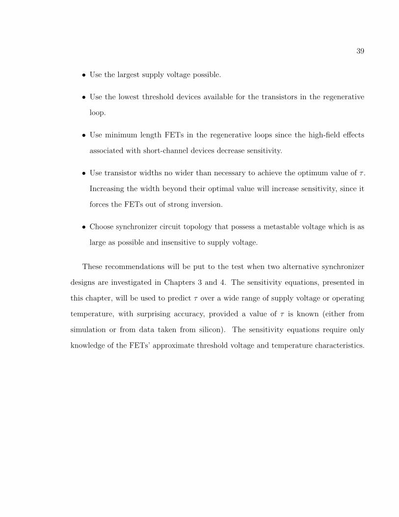
39
• Use the largest supply voltage possible.
• Use the lowest threshold devices available for the transistors in the regenerative
loop.
• Use minimum length FETs in the regenerative loops since the high-field effects
associated with short-channel devices decrease sensitivity.
• Use transistor widths no wider than necessary to achieve the optimum value of τ .
Increasing the width beyond their optimal value will increase sensitivity, since it
forces the FETs out of strong inversion.
• Choose synchronizer circuit topology that possess a metastable voltage which is as
large as possible and insensitive to supply voltage.
These recommendations will be put to the test when two alternative synchronizer
designs are investigated in Chapters 3 and 4. The sensitivity equations, presented in
this chapter, will be used to predict τ over a wide range of supply voltage or operating
temperature, with surprising accuracy, provided a value of τ is known (either from
simulation or from data taken from silicon). The sensitivity equations require only
knowledge of the FETs’ approximate threshold voltage and temperature characteristics.

40
CHAPTER 3
DESIGN AND CHARACTERIZATION OF A STANDARD FLIP-FLOP USED AS A
SYNCHRONIZER
In this chapter, a design is presented to verify the validity of predicting trends in
metastability parameters in the presence of process variation through sensitivity analysis.
First, a simple design will be chosen and discussed in detail. A discussion of optimization
performed on the topology in order to make it a reasonable synchronizer cell will follow.
Physical layout of the design will be discussed due to the fact that parasitics associated
with wiring capacitances can be significant in submicron designs. The operation of the
circuit will next be verified using standard industry metrics such as tCLK−Q, setup, and
hold times. Finally, MetaACE will be used to show the how well the sensitivity equations
developed in Chapter 2 predict and model the variation of τ due to temperature, threshold,
and power supply variations.
3.1 Design Objectives
One goal of this thesis is to examine practical designs that might be implemented
as synchronizers in modern SoCs. Bearing this in mind, a common circuit topology was
selected. There are a variety of circuits that could be chosen, but a simple Master-Slave D
flip-flop was chosen due to the ubiquitous nature of this device in modern chips, coupled
with its relatively simple operation.
The Master-Slave flip-flop is made of two simple level sensitive multiplexer-based
latches. This design takes two inverters in a regenerative loop broken by a two-to-one
multiplexer. In most designs the multiplexer is constructed using transmission gates as
seen in Figure 3.1 [Rabaey, 2003, pg. 305]. First a brief description of circuit operation is
covered.
A multiplexer-based latch possesses two states. The first state is when the input
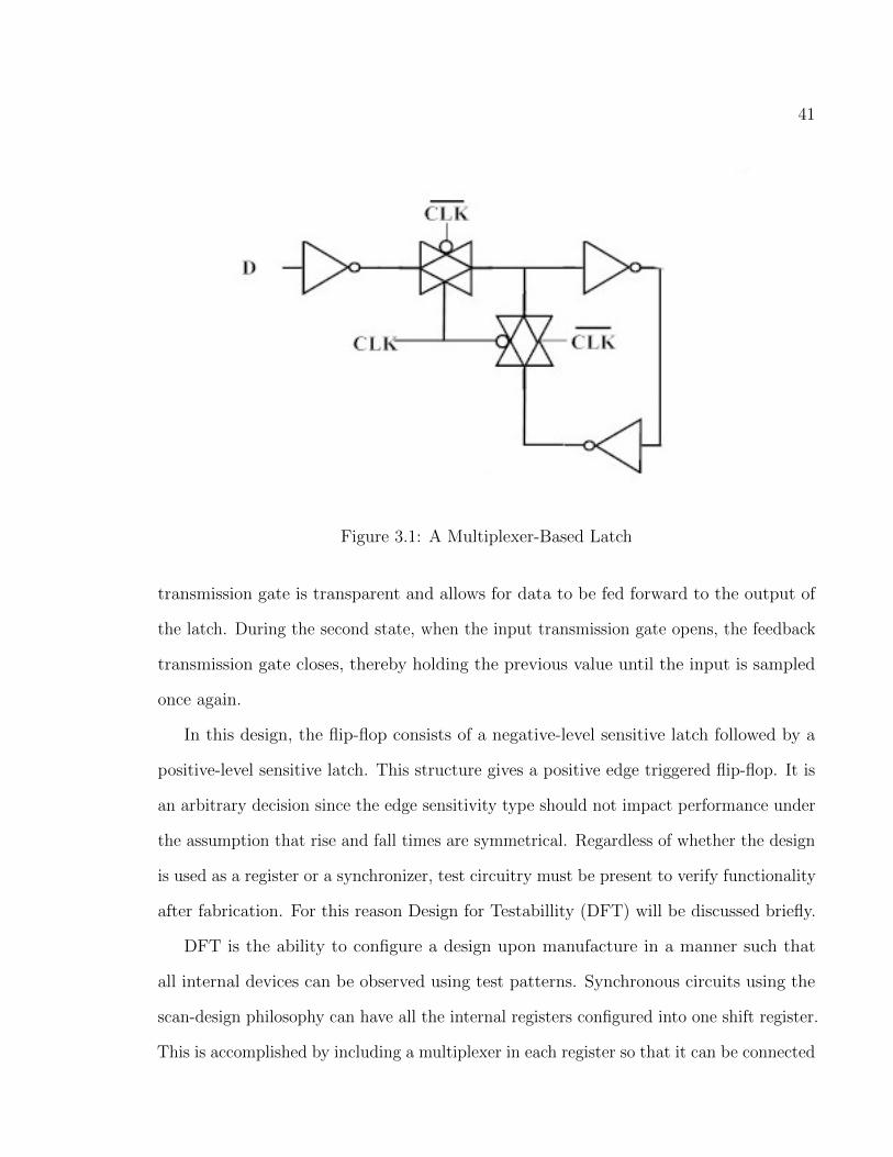
41
Figure 3.1: A Multiplexer-Based Latch
transmission gate is transparent and allows for data to be fed forward to the output of
the latch. During the second state, when the input transmission gate opens, the feedback
transmission gate closes, thereby holding the previous value until the input is sampled
once again.
In this design, the flip-flop consists of a negative-level sensitive latch followed by a
positive-level sensitive latch. This structure gives a positive edge triggered flip-flop. It is
an arbitrary decision since the edge sensitivity type should not impact performance under
the assumption that rise and fall times are symmetrical. Regardless of whether the design
is used as a register or a synchronizer, test circuitry must be present to verify functionality
after fabrication. For this reason Design for Testabillity (DFT) will be discussed briefly.
DFT is the ability to configure a design upon manufacture in a manner such that
all internal devices can be observed using test patterns. Synchronous circuits using the
scan-design philosophy can have all the internal registers configured into one shift register.
This is accomplished by including a multiplexer in each register so that it can be connected
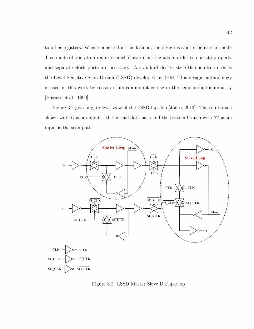
42
to other registers. When connected in this fashion, the design is said to be in scan-mode.
This mode of operation requires much slower clock signals in order to operate properly,
and separate clock ports are necessary. A standard design style that is often used is
the Level Sensitive Scan Design (LSSD) developed by IBM. This design methodology
is used in this work by reason of its commonplace use in the semiconductor industry.
[Bassett et al., 1990].
Figure 3.2 gives a gate level view of the LSSD flip-flop [Jones, 2013]. The top branch
shown with D as an input is the normal data path and the bottom branch with SI as an
input is the scan path.
Figure 3.2: LSSD Master Slave D Flip-Flop

43
3.2 Optimization of Gain Bandwidth Product of Inverter Loops
As stated in previous chapters, the dominant parameter in the MTBF equation is τ .
The term containing τ is exponential which will give the most significant performance
increase. This section will explain the relationship between τ and the gain-bandwidth
product (GBW) of an inverter loop, then explain how one can maximize GBW. This
section will now demonstrate that
τ (a metastability parameter) ∝ 1
GBW (a circuit parameter). (3.1)
Figure 3.3: Linearly Cascaded Amplifiers
Small-signal analysis will be used to verify this relationship and determine the propor-
tionality constant between τ and GBW. This analysis begins with the assumption that the
inverters will be acting as cascaded linear amplifiers as in Figure 3.3. The low-frequency
open-loop gain of these two identical amplifiers can be given as
A1 = −gmro (3.2)
A2 = −gmro (3.3)
It is assumed that each amplifier drives some load and output capacitance and with

44
this information settling time constants can be given as
τ1 = roCL1 (3.4)
τ2 = roCL2. (3.5)
The total low-frequency open-loop gain can be written as the product of the two amplifier
gains,
ADC = A1A2 = (gmro)2. (3.6)
Using open circuit time constant analysis, [Razavi, 2001] the dominant pole frequency is
ω0 ≈1
τ1 + τ2
=1
ro(CL1 + CL2). (3.7)
GBW is defined as the product of the dominant pole frequency and the low-frequency
gain,
GBW =ω0
2πADC . (3.8)
Substituting and rearranging, one may write
2πGBW =(gmro)
2
ro(CL1 + CL2)= gmro
[gm
CL1 + CL2
](3.9)
2πGBW = (gmro)
(CL2
CL1 + CL2
)(gmCL2
). (3.10)
But
CL2
gm= τ (3.11)
and therefore
τ = (gmro)
(CL2
CL1 + CL2
)(1
2πGBW
). (3.12)
Recalling that ADC = (gmro)2
τ =[r√ADC
] [ 1
2πGBW
](3.13)

45
where
r =CL2
CL1 + CL2
. (3.14)
Typically, CL1 is close to CL2 so r ≈ 0.5 (in reality CL2 > CL1).
The preceding analysis has shown that with the appropriate information, τ can be
numerically predicted. It is also clear from the preceding analysis that in order to
maximize MTBF, τ must be minimized. Alternatively, GBW must be maximized in order
to maximize MTBF.
There are two degrees of freedom a designer has in maximizing GBW, shape factor
and threshold voltage (assuming a fixed supply voltage). Shape factor gives a designer the
most freedom, while threshold voltages are more restrictive in digital designs. If a designer
wants a faster circuit, a smaller threshold voltage is better. Unfortunately, this comes
at the cost of power consumption. Low threshold voltage devices increase short-circuit
power dissipation, and leakage currents for a MOSFET are inversely and exponentially
dependent upon threshold voltage [Rabaey, 2003] [Tsividis, 2011].
The assumption is made that the low-frequency open-loop gain does not vary with the
changing of transistor widths in the amplifier. In the simulator NFET widths of 90 nm to
900 nm (PFETs using 140 nm to 1400 nm) were used to see how much the low-frequency
gain varied. The value differs only by 0.1 dB. Therefore, the gain will not be dramatically
affected by varying transistor widths.
3.3 Transistor Sizing
Transistor size is determined by the width and the length of the device. In high-speed
circuits minimum length is always used, so width is the only degree of freedom available
to the designer.
Characterization of the transistors is necessary to develop appropriately sized devices
for a fully complementary design style. The basic building block of this design style is
the inverter. For consistency, the rise and fall times of the circuits are assumed to be

46
symmetrical. PFETs inherently operate more slowly because of their lower mobility. To
account for this, the PFET is made wider to reduce its timing resistance. To determine the
width ratio of a PFET to a NFET, a simple testbench with an inverter was constructed.
In the testbench, a simple CMOS inverter circuit is driven by a buffer from a standard
cell library and the inverter drives a capacitive load of 1 fF. This load is large enough
that the output capacitance of the inverter has little effect on the charging time. Rise and
fall times are measured while sweeping the width of the PFET to determine the timing
resistance. The appropriate width ratio of PFET to NFET was found and rounded to
1.5. The design process proceeded to optimization of the inverter loop devices. Cadence’s
electrical simulator Spectre R© was used for simulation.
Figure 3.4: Small Signal Testbench for The Master Loop
The testbench for the Master loop is designed first, as seen in Figure 3.4. The
transmission gate devices are biased so as to turn on. The reason for this is that τ is
very sensitive to capacitance. To make certain the capacitance is consistent with normal

47
operation, the inverters connecting the loop to the next stage are kept in the model. The
AC signal is applied to the feedback inverter’s input through an enormous capacitor. The
capacitor cannot be manufactured, rather it makes certain that the AC source does not
contribute to biasing. At DC the capacitor is an open circuit, and during AC the capacitor
acts as a short. To make sure that the circuit acts as two cascaded linear amplifiers the
loop has to be broken. This is easily accomplished by adding a very large inductor in
the loop. The large inductor in the circuit acts as a short for the DC solution, and acts
as an open for the AC analysis. In the image, the inverters with sizes being varied are
designated with a W .
The testbench for the Slave loop seen in Figure 3.5 follows the same design procedure
as the Master loop. The loop is broken with a large inductor and the AC source is isolated
from the DC solution by the large capacitor. The GBW measured for this loop is expected
to be inherently smaller due to the contribution of extra capacitance from more loop
devices.
Transistors are sized by running an OCEAN script to determine the maximum GBW
of the inverter loop configured as an amplifier. This script performs an AC analysis and
queries the simulator to obtain the GBW for given device sizes. It is assumed in this
work that the loop inverters are the same size. Each iteration returns a value for GBW.
This is then plotted against the width of the given devices as can be seen in Figures 3.6
and 3.7. With the given graphs, it is obvious that 270 nm will give a reasonable value to
maximize GBW.
As was demonstrated in Chapter 2, increasing the width beyond what is absolutely
necessary increases variability with minimal improvement in τ . The design choice in the
paragraph above allows savings in terms of area while still giving near optimal performance
and good resilience against variability.
Figures 3.6 and 3.7 also show a very useful piece of information in regards to layout.

48
Figure 3.5: Small Signal Testbench for The Slave Loop

49
The family of curves given show that in the Master loop, the GBW does not increase
significantly if the devices are made wider, even at a load of 10 fF. The Slave loop has a
less pronounced curvature in near vicinity of the maximum than the Master.
Figure 3.6: GBW as a Function of Device Width for The Master Loop
There is no method that is well suited to determine the capacitance on the critical
methods for this process, so different values were plotted to give an idea of the effects. It
was estimated that the amount of capacitance on critical nodes will be under 10 fF.
To give a more quantitative view, Tables 3.1 and 3.2 give the values of GBW under
different conditions. These conditions include different device widths and different
capacitances. In Table 3.1 wiring capacitance is not added. In Table 3.2 device width is
chosen to be 270 nm.
Table 3.1 implies that there is not much benefit to increasing the width above 270 nm
in either loop. There is no benefit from making loop devices very large, and in fact, can
lead to a less than optimal synchronizer cell.
Table 3.2 gives values of GBW in GHz for the Master and Slave loops based upon

50
Figure 3.7: GBW as a Function of Device Width for The Slave Loop
NFET Width (nm) Master GBW (GHz) Slave GBW (GHz)
90 85 37
180 110 57
270 117 66
360 117 69
450 115 68
Table 3.1: GBW for Device Width in The Master and Slave Loops (no wiring capacitance)
Using a VTL Design

51
additional wiring capacitance. It becomes clear that GBW decreases with increases in
wiring capacitance. Raising the wiring capacitance by an order of magnitude from 1 fF to
10 fF drops the GBW of a given loop by about a third.
Master GBW (GHz) Slave GBW (GHz)
No capacitance 117 66
1 fF 94 56
2 fF 78 49
4 fF 58 39
10 fF 32 24
Table 3.2: GBW for Different Values of Wiring Capacitance (width of 270 nm) Using
VTL
Further observation of Table 3.2 shows that the Master loop’s GBW is almost twice
that of the Slave loop. This implies that there is significantly less capacitance due to the
devices in the Master compared to the Slave loop. It can further be interpreted that the
capacitance due to devices in the Slave loop is between 2 fF and 4 fF higher than the
Master loop.
3.4 Physical Layout
In a normal design flow, physical layout is performed to model wiring capacitances
associated with a fabricated circuit. An image of the complete layout is presented in
Figure 3.8. The tools used include the following:
• Arizona State University’s (ASU) Non-manufacturable 45 nm Process
• North Carolina State University’s (NCSU) 45 nm Process Design Kit
• Nangate’s 45 nm Standard Cell Library

52
Figure 3.8: Physical Layout for a LSSD Master-Slave D Flip-Flop
A few design rules are imposed upon the layout so as to model a typical standard
cell. The basis for the dimensions of the cell are modeled after Nangate’s open cell library
using the NCSU design kit. The design simply follows the width of the cell, the width of
power rails, the distance between rails, and the distance between the rails and the edges
of the well. Values used in the layout for spacing are given in Table 3.3 for reference.
Cell Width 1.63 µm
VDD/VSS Width 0.17 µm
Distance Between Rails 1.23 µm
Well Past Rails (Vertical) 0.03 µm
Well Past Rails (Horizontal) 0.115 µm
PWELL Width 0.925 µm
NWELL Width 0.705 µm
Table 3.3: Standard Cell Rules
The layout is not perfect, but it is sufficient for the simulations prepared in this thesis.
A multi-stage synchronizer can be formed by cascading copies of the layout. This was
done so that during tests, the first synchronizer will see a typical load. The synchronizer
layouts created include three different types of configurations: VTL, VTG, and VTG using
VTL in the regenerative loops. Utilization of these devices only requires an additional

53
layer of material on top of the basic VTL devices in the NCSU PDK.
The final layout of the optimized cell is measured to be 1.63 µm x 9.6 µm or an area
of 15.65 µm2. The two stage synchronizer is measured to be 1.63 µm x 19.2 µm or an
area of 31.3 µm2.
Since the two stage circuit is not considered as a standard cell for the purposes of this
project, metal layers M3 and M4 were permitted for the combining of the layouts.
With layout completed, a functional comparison between physical layout and drawn
schematics is necessary. Mentor Graphics’s Calibre is used for Design Rule Check (DRC)
and Layout Versus Schematic (LVS) checks. These tools helped determine that the layout
and schematic are functionally equivalent.
Next, the importance of parasitic extraction is discussed. Parasitic extraction is
the process of including intrinsic resistances and capacitances that arise in a physical
layout. Calibre’s xRC tool was used for generation of the netlist. The netlist generated
was in HSPICE format and needed to be put into Spectre format for functional design
verification.
After parasitic extraction, the netlist was excessively large. Simulations were performed
in MetaACE and the time it took to simulate was very long (hours) for even simple tests.
A second netlist without extracted resistances was generated and tested. Overall the
difference between results from MetaACE for this smaller circuit was under 3% while the
number of nodes in the netlist decreased by a factor of four. Given the accuracy of the
reduced netlist as well as the savings, this new netlist is deemed suitable for work in this
thesis.
3.5 Design Verification
With design work, layout, and extraction completed, verification of the design’s
predicted performance is the next key step. There are three parameters which are used for
verification of the design: setup time, hold time, and tCLK−Q. Table 3.4 gives a concise

54
summary of these values.
VTL VTG
tSU schematic 26 ps 28 ps
tSU extracted 36 ps 46 ps
tH schematic 0 ps 0 ps
tH extracted 0 ps 0 ps
tCLK−Q schematic 28 ps 44 ps
tCLK−Q extracted 55 ps 83 ps
Table 3.4: A Table of Setup, Hold, and tCLK−Q for Different Threshold Voltages
As is to be expected, the lower threshold VTL devices perform more quickly. Pure
VTL designs allow the smallest setup and hold times, as well as the shortest delay through
the flip-flop, tCLK−Q. Even after extraction, there is not a significant change on the setup
time for VTL. In VTG circuits there is a more noticeable change in setup time. The hold
times are all zero, which is an ideal case so as to lower the chance of becoming metastable
because of the reduced time window.
The tests used for design verification of the data chain involve driving the inputs with
buffered clock and data signals. The output Q drives a 1 fF capacitor. The scan chain
inputs are also buffered and the output SO drives a 1 fF capacitor. Since the scan chain
is not of great interest and is not intended for use outside of testing after fabrication, it is
not characterized.
The first step in verifying design parameters is to determine the method of testing
for each parameter. The tests all assume measurement from the 50% point of the rising
edge of a waveform. To measure tCLK−Q the flop is run in normal operation. Normal
operation in this context implies the following:

55
• The data frequency is half that of the clock frequency
• The rising edge of the data is at 3/4 of the way into the clock period
• Rising and falling edges of clock and data are symmetric
• The entire circuit drives a fixed load
• The scan chain is to be idle
With the given criteria, the testbench is configured in this manner. The flip-flop was
run in this setting and a measurement is made from the midpoint of the rising edge of
the clock (CLK) to the rising edge of the output (Q). This method is used for both the
schematic and extracted views and recorded.
The setup times are measured by bring the rising edge of the data progressively closer
to the clock edge. Once the output no longer registers the input value, the setup time
is considered violated. The pulse width had to be modified such that the data was not
high at the beginning of a future clock cycle. The hold times were measured by fixing the
rising edge of the data signal at a point three quarters of the way into the clock period
while the falling edge is pulled closer to the clock edge. This is done until the falling edge
of the data is coincident with the rising edge of the clock. The falling edge is not pulled
further back because data must remain stable during the setup time window.
3.6 Dependence of τ on Supply Voltage
After design verification is completed, the circuit is ready to be used with MetaACE
to verify the sensitivity analysis presented in Chapter 2. The designs to be explored in
this section and the proceeding sections include VTL and VTG devices. There are three
designs that will be presented in this section :
• a design using only VTL transistors

56
• a design using only VTG transistors
• a design using VTL transistors in the regenerative loops and VTG everywhere else
The following conditions were used for simulation with MetaACE:
• Temperature of 25 ◦C
• Supply Voltage ranging from 0.8 V to 1.2 V in 0.1 V increments
• Initial Setup Time value is set to 5e-10
• Data Rate of 133 MHz
• Clock Rate of 200 MHz
Tables with Master, Slave, and effective τ ’s are presented to give a quantitative view
of the effect of different supply voltages. The values presented in the tables were collected
from MetaACE. Plots are presented which compare the results of sensitivity analysis to
the values gathered from MetaACE. Tables of the sensitivity of τ to supply voltages are
shown.
VDD (V) τm (ps) τs (ps) τeff (ps)
0.8 14 29 19
0.9 11 22 15
1.0 10 19 13
1.1 9 17 12
1.2 8 16 11
Table 3.5: τ for Different Supply Voltages Using Only VTL Devices
It can be seen from the tables that the Master and Slave τ ’s are different and thus,
the effective τ equation must be used to give an idea of the circuit’s ability to exit
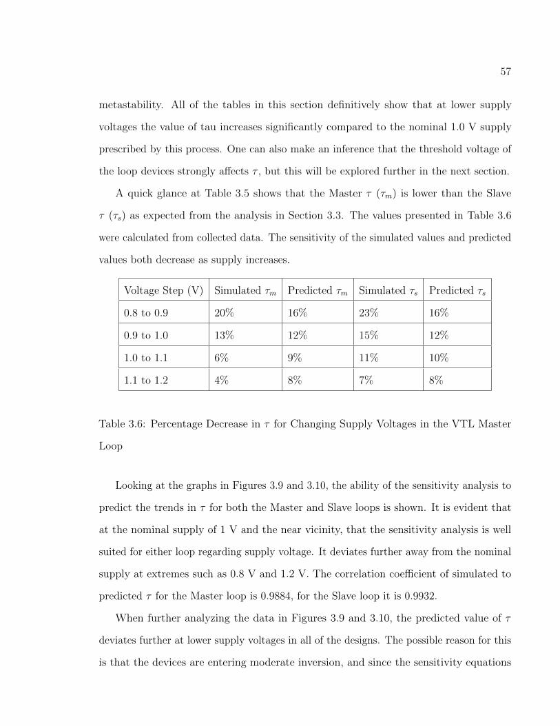
57
metastability. All of the tables in this section definitively show that at lower supply
voltages the value of tau increases significantly compared to the nominal 1.0 V supply
prescribed by this process. One can also make an inference that the threshold voltage of
the loop devices strongly affects τ , but this will be explored further in the next section.
A quick glance at Table 3.5 shows that the Master τ (τm) is lower than the Slave
τ (τs) as expected from the analysis in Section 3.3. The values presented in Table 3.6
were calculated from collected data. The sensitivity of the simulated values and predicted
values both decrease as supply increases.
Voltage Step (V) Simulated τm Predicted τm Simulated τs Predicted τs
0.8 to 0.9 20% 16% 23% 16%
0.9 to 1.0 13% 12% 15% 12%
1.0 to 1.1 6% 9% 11% 10%
1.1 to 1.2 4% 8% 7% 8%
Table 3.6: Percentage Decrease in τ for Changing Supply Voltages in the VTL Master
Loop
Looking at the graphs in Figures 3.9 and 3.10, the ability of the sensitivity analysis to
predict the trends in τ for both the Master and Slave loops is shown. It is evident that
at the nominal supply of 1 V and the near vicinity, that the sensitivity analysis is well
suited for either loop regarding supply voltage. It deviates further away from the nominal
supply at extremes such as 0.8 V and 1.2 V. The correlation coefficient of simulated to
predicted τ for the Master loop is 0.9884, for the Slave loop it is 0.9932.
When further analyzing the data in Figures 3.9 and 3.10, the predicted value of τ
deviates further at lower supply voltages in all of the designs. The possible reason for this
is that the devices are entering moderate inversion, and since the sensitivity equations

58
Figure 3.9: Predicted vs. Simulated τ for VTL Master Loop Devices
Figure 3.10: Predicted vs. Simulated τ for VTL Slave Loop Devices

59
were developed for strong inversion, some error is to be expected. Moderate inversion
mainly implies that diffusion currents are now becoming more prevalent and are on the
same order of magnitude as drift current.
VDD (V) τm (ps) τs (ps) τeff (ps)
0.8 34 87 48
0.9 20 47 28
1.0 14 31 19
1.1 12 24 16
1.2 10 21 14
Table 3.7: τ for Different Supply Voltages Using Only VTG Devices
In order to see if results predicted are consistent, MetaACE was used to collect data
from VTG designs and then the sensitivity analysis script was run. Table 3.7 shows
the values collected from MetaACE. From Table 3.8 the trend in decreasing sensitivity
for higher supply voltages continues. The sensitivity is also higher for higher threshold
voltages, reaffirming the claim that for PVT-tolerant designs one should use low threshold
voltage devices in the loop.
Figure 3.11 shows the effectiveness of the sensitivity analysis still holds for a design
with a higher threshold voltage. As mentioned previously, the high field effects can be
neglected when analyzing the VTG devices, and the prediction still maintains a solid
accuracy, only deviating significantly at 0.8 V (due to entering moderate inversion). The
correlation coefficient for Figure 3.11 is 0.9928.
In the current market, low-power ICs are very desirable. With deep submicron (DSM)
technologies the issue of static power dissipation is an ever pressing concern as well
as short-circuit conduction. A higher threshold voltage leads to lower leakage currents

60
Voltage Step (V) Simulated Predicted
0.8 to 0.9 46% 33 %
0.9 to 1.0 34% 25%
1.0 to 1.1 29% 20 %
1.1 to 1.2 15% 17%
Table 3.8: Percentage Decrease in τ for Changing Supply Voltages in the VTG Master
Loop
Figure 3.11: Predicted vs. Simulated τ for VTG Master Loop Devices
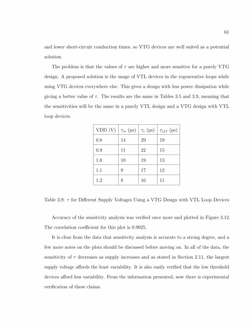
61
and lower short-circuit conduction times, so VTG devices are well suited as a potential
solution.
The problem is that the values of τ are higher and more sensitive for a purely VTG
design. A proposed solution is the usage of VTL devices in the regenerative loops while
using VTG devices everywhere else. This gives a design with less power dissipation while
giving a better value of τ . The results are the same in Tables 3.5 and 3.9, meaning that
the sensitivities will be the same in a purely VTL design and a VTG design with VTL
loop devices.
VDD (V) τm (ps) τs (ps) τeff (ps)
0.8 14 29 19
0.9 11 22 15
1.0 10 19 13
1.1 9 17 12
1.2 8 16 11
Table 3.9: τ for Different Supply Voltages Using a VTG Design with VTL Loop Devices
Accuracy of the sensitivity analysis was verified once more and plotted in Figure 3.12.
The correlation coefficient for this plot is 0.9925.
It is clear from the data that sensitivity analysis is accurate to a strong degree, and a
few more notes on the plots should be discussed before moving on. In all of the data, the
sensitivity of τ decreases as supply increases and as stated in Section 2.11, the largest
supply voltage affords the least variability. It is also easily verified that the low threshold
devices afford less variability. From the information presented, now there is experimental
verification of these claims.

62
Figure 3.12: Predicted vs. Simulated τ for VTG Design with VTL Loop Devices
3.7 Dependence of τ on Threshold Voltage
The next parameter of interest is the threshold voltage. Modern processes and
technologies afford the option of different threshold voltages in devices so that designers
have the option of higher speed (low threshold voltage) or lower static power dissipation
(higher threshold voltage) designs. Even with these options, there will be mismatches
between threshold voltages of devices in different production runs and even on chip due
to random factors. It is thus important to predict trends in τ due to variations in the
threshold voltage.
There is not an easy way to alter the threshold voltage of the models slightly for
the purposes of sensitivity analysis verification in this process. As a way to verify the
effects of threshold voltage, a prediction of τ for a VTG design was generated from a
VTL design’s data.
As seen in Figure 3.13, The sensitivity equation predicts what τ might be at a higher
threshold with good accuracy at higher supply voltages and less accuracy (due to moderate
inversion) at lower supply voltages. Using the nominal supply of 1.0 V, the difference
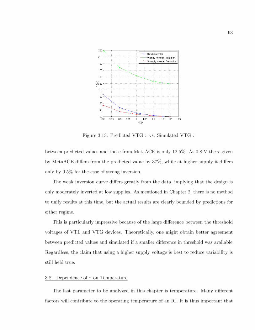
63
Figure 3.13: Predicted VTG τ vs. Simulated VTG τ
between predicted values and those from MetaACE is only 12.5%. At 0.8 V the τ given
by MetaACE differs from the predicted value by 37%, while at higher supply it differs
only by 0.5% for the case of strong inversion.
The weak inversion curve differs greatly from the data, implying that the design is
only moderately inverted at low supplies. As mentioned in Chapter 2, there is no method
to unify results at this time, but the actual results are clearly bounded by predictions for
either regime.
This is particularly impressive because of the large difference between the threshold
voltages of VTL and VTG devices. Theoretically, one might obtain better agreement
between predicted values and simulated if a smaller difference in threshold was available.
Regardless, the claim that using a higher supply voltage is best to reduce variability is
still held true.
3.8 Dependence of τ on Temperature
The last parameter to be analyzed in this chapter is temperature. Many different
factors will contribute to the operating temperature of an IC. It is thus important that

64
temperature and its effects on τ be taken into account. To give a wide coverage, the
automotive temperature rating, ranging from -40◦C to 125◦C, described in Section 1.4
will be used.
τ is predicted to increase with temperature in a strongly inverted device in Section
2.9. Figures 3.14 and 3.15 show a comparison of the simulated values of τ and the
predicted values. For the Master loop temperature predictions, the maximum measured
error compared to the values from MetaACE is only 9% , while the Slave loop error is
only 6%. Both the Master and Slave loop predictions have a correlation coefficient of
0.998 when compared to the simulated values. Like in Section 3.6, only the Master loops
will be discussed further for the sake of brevity.
Figure 3.14: Predicted vs. Simulated τ for VTL Master Loop Devices in the Automotive
Temperature Range
It is important to see how well the sensitivity equations work in different scenarios.
This was accomplished by running temperature simulations for the designs described in
Section 3.6. Figure 3.16 shows a comparison between results from MetaACE and results

65
Figure 3.15: Predicted vs. Simulated τ for VTL Slave Loop Devices in the Automotive
Temperature Range
of the sensitivity equations. When data points were compared, the maximum deviation
from the values produced by MetaACE was only about 5% and a correlation coefficient
of 0.998.
The final circuit used for comparison is the design which uses VTL devices in the
regenerative loops and VTG devices everywhere else. The maximum error between the
predicted and simulated values in Figure 3.17 is about 7% and a correlation coefficient of
0.999.
The graphs show some anomalous behavior as temperature increases. One should
expect a smoothly increasing value in τ over the temperature range, but in the graphs
there are some points which may not strictly increasing between temperatures. This is
attributed to numerical errors produced by MetaACE.
Theoretically in the weak inversion regime, there is a point where cold temperatures
are worst case. This was unable to be adequately demonstrated using this process because
the temperature coefficient k2 was determined to be -0.2 mV◦C
. This value is so small that
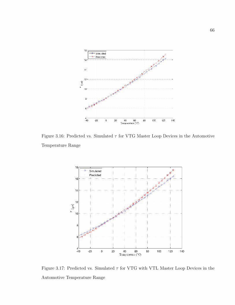
66
Figure 3.16: Predicted vs. Simulated τ for VTG Master Loop Devices in the Automotive
Temperature Range
Figure 3.17: Predicted vs. Simulated τ for VTG with VTL Master Loop Devices in the
Automotive Temperature Range

67
demonstrating the cold temperature being worst case proved too difficult and is left as
future work.
In this chapter a circuit that could be used as a basic synchronizer was presented. It
was demonstrated that GBW must be maximized in order to minimize the value of τ . A
method for determining device size based upon maximizing GBW of a small signal circuit
was presented and used. Physical layouts were described and netlists were generated for
use in MetaACE. The operation of the design was verified and values for parameters of
interest to a designer were given.
In the last few sections the ability of the sensitivity equations to predict different
values of τ is confirmed. The sensitivity of τ to supply voltage was verified. A few ideas on
PVT tolerant design were verified. Section 3.6 accurately demonstrated that variation of τ
with supply voltage decreases for higher supplies, as well as the importance of using lower
threshold devices in the regenerative loops. Section 3.7 showed the ability to predict with
some accuracy the value of τ for a device with a different threshold voltage, particularly
with higher supply voltages. Finally, temperature effects and the accuracy of τ predicted
by the sensitivity equations was presented.

68
CHAPTER 4
DESIGN AND CHARACTERIZATION OF A SPECIALIZED SYNCHRONIZER CELL
In this chapter, an alternative synchronizer cell will be explored and optimized as was
done in Chapter 3. The purpose of this chapter is to show the general applicability
of the equations developed in Chapter 2 to other possible types of designs. To this
end, a significantly different topology is given as well as a description of its operation,
optimization, layout, and verification. Finally, comparisons between results from MetaACE
and the sensitivity equations will be discussed.
4.1 Design Objectives and Overview
In Chapter 3 the design procedure of a simple synchronizer cell is covered in great
detail. In order to demonstrate the generality and topology independence of sensitivity
analysis, a drastically different topology is explored in this chapter.
There are several different circuit schemes for flip-flops as well as dedicated synchronizer
designs. In the previous chapter a basic data register was considered in the role of a
synchronizer circuit. The aim of this chapter is to pick a circuit that is primarily used
as a synchronizer and show that the sensitivity analysis still holds outside the case of a
simple data register.
Designers have proposed the Jamb latch as a way of improving synchronizer perfor-
mance. The Jamb latch is similar to a traditional data latch in topology but slightly
modified. It eliminates series connected transistors giving it better metastability resolu-
tion, but there are still issues. For larger feature sizes, this circuit performs adequately,
but in deep sub-micron processes, these assumptions fail. It relies on the NFETs having
about twice the drive strength of a PFET. Due to velocity saturation becoming more
prevalent in smaller feature sizes, this assumption fails to hold. NFETs will saturate
more quickly than a typical PFET device, meaning that the transconductance will be less

69
than that of a classically saturated FET. To avoid this, the NFET would have to made
too large for practical purposes. Yang, Jones, and Greenstreet have proposed a modified
Jamb latch to solve this problem.[Yang et al., 2011, pp. 34-35]
Figure 4.1 gives the schematic of the latch proposed by Yang, et. al. Designers
typically use synchronizers in chains till the required MTBF is met. In most cases, the
last flip-flop in the chain does not contribute to metastability resolution. It is thus the
job of the first n-2 latches to resolve metastability. A synchronizer is a variant of a sense
amplifier, with the difference being that the offset trimming circuitry is omitted. Since
the first n-2 stages of the synchronizer are concerned with resolving metastability, the
signals do not have to be full swing logic levels. This task is left to the last flip-flop in a
synchronizer chain. Figure 4.1 is based upon these principles [Yang et al., 2011, pg. 40].
A brief description of the operating behavior of such a latch is given below.
Figure 4.1: A Pseudo-NMOS Latch Schematic
When the RESOLVE signal is held low, the PFETs will conduct acting as pull-up
devices for both Q and Q. At the same time, if D is high and D is low, There will be
a fight for pulling Q low. Since Q is not being pulled low, it will be allowed to resolve
high. The end result in this scenario is Q resolving high, and Q at some lower value.

70
When RESOLVE goes high, the pull-down transistors gated by RESOLVE create a virtual
ground, allowing the circuit to latch in Q and Q to settle to some value close to ground.
The behavior when D is low and D is high lead to a similar situation. If D and D change
or have ill-defined values, regenerative multiplication takes place. Since D and D do not
need to be logic signals, The Q and Q signals can be directly connected from one latch to
the inputs of another. Due to the lessened capacitive load and high gm, this circuit can
achieve much lower values of τ [Yang et al., 2011, pg. 40].
The overall architecture of the flip-flop must be considered before sizing devices. As
before the flip-flop will be a Master-Slave circuit with scan, but using a different technique
than Chapter 3. In the previous chapter, there were effectively two input branches which
were identical, and they were multiplexed before reaching the output latch. In this design,
the inputs are multiplexed before reaching the latches. The multiplexer needed to be
able to pass not one, but two signals since these flip-flops are driven differentially. The
new topology still needs a scan out latch, but this latch does not have to be a dedicated
synchronizer, as it is used for tests, not typical operation. In the design proposed, a
multiplexer-based latch like the one used in Chapter 3 is chosen for simplicity.
The design chosen comes from a patent held by Oracle R© with some slight modifications
[Jones et al., 2013, Fig. 4C]. Figure 4.2 shows the schematic with modifications. The
main difference between schematics is the elimination of two NOR gates and the inclusion
of an XOR gate. The input consists of four tri-state inverters. These, through the use
of CLK, and SI CLK as control signals, form the input multiplexer. Following the
multiplexer is a pull-up network. This ensures that the input is pulled high in the event
of both SI CLK and CLK being held low.
The complements of CLK and SI CLK are generated in the schematic rather than
driven by pins. This is to simplify the top level testbench and keep it less cluttered. To
keep the differential signals un-skewed before being input, they are kept as individual
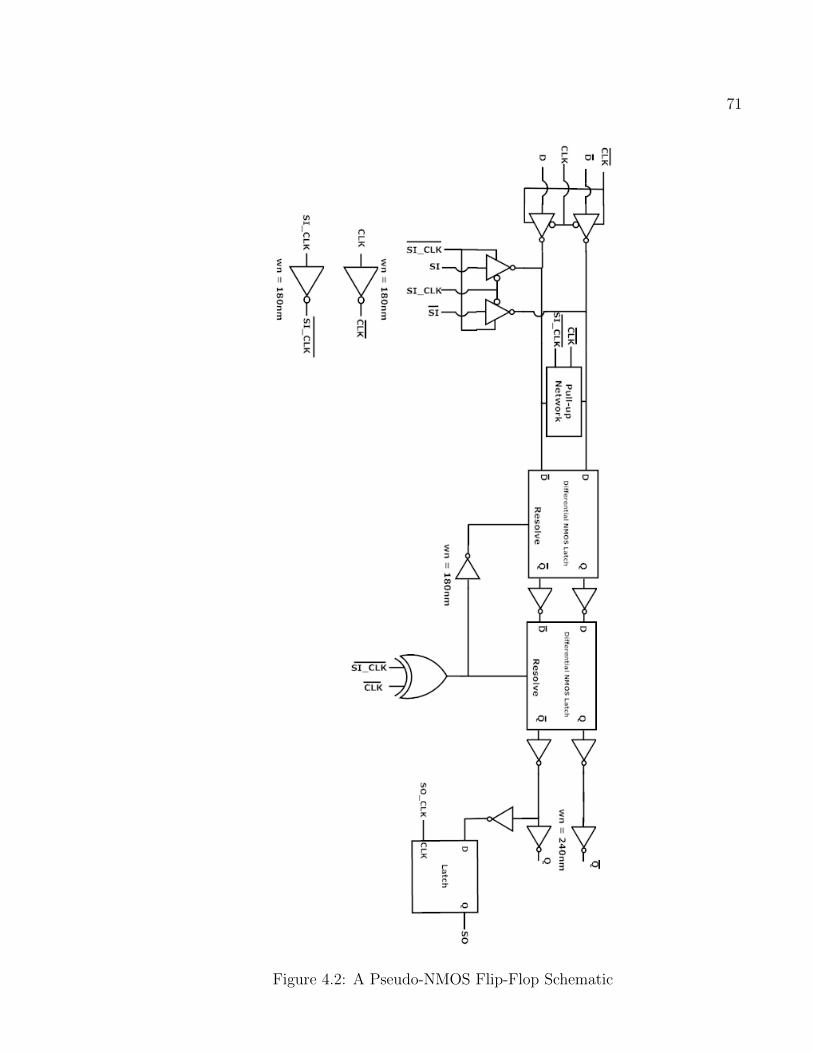
71
Figure 4.2: A Pseudo-NMOS Flip-Flop Schematic

72
pins in the top level.
The latches are placed after the pull-up network and driven by the logical XOR of
CLK and SI CLK. In order to make the flip-flop rising-edge triggered, the first latch
must be logic level high sensitive and the second must be logic level low sensitive. The
design uses the XOR operation as stated above to generate the overall clock signals for
the latch. Using this method eliminates the need of a separate branch as used in the
first design. This signal is fed to both latches’ RESOLVE pin, but the first latch has an
inverter before it. Although the inverter adds some delay between the signals, in testing
it was seen to be small enough to not affect operation.
Inverters are placed from the output of the first latch to the input of the second
latch to make certain that loading capacitance of the second latch doesn’t heavily impact
metastability resolution capability. Inverters are placed at the output of the second latch
to make the design tolerant to different loads much like the first latch. This also gives the
added benefit of both latches having the same value of τ which was seen in Section 1.3 to
be ideal for synchronizer design.
The content analyized in this chapter will be reduced for simplicity by using results
from a purely VTL design. The trends given in previous work are sufficient to warrant a
reduced study in this chapter. The goal is to simply show that the predicted trends in
the sensitivity analysis are sufficient that assumptions can be made regarding different
devices.
4.2 Optimization of Gain Bandwidth Product of Inverter Loops
As in Chapter 3, GBW is a critical parameter in the design of a synchronizer. With
the optimization of GBW for a topology, one can theoretically develop the best possible
synchronizer. This will give the designer the ability to size the transistors, and predict
trends in τ due to things such as wiring capacitance or temperature.
The analysis once again will be used to maximize the GBW due to the inverse
73
relationship with τ as shown in Section 3.2. It is worth noting that the values of GBW
presented in the next section are notably higher, but are not necessarily representative of
an ideal synchronizer’s performance.
The reason is that the topology proposed suffers significantly from the body effect, and
the process used in this thesis cannot avoid the body effect. While the sizing method used
in the next section is theoretically useful, due to process limitations and time constraints
a simplified view is taken.
4.3 Transistor Sizing
In this latch the fully complementary design philosophy is abandoned in favor of a
pseudo-NMOS design style. This means that the PFET width will not be varied, but
rather, their length. The length is used to determine the output resistance necessary. The
NFET width is still optimized while using the minimum length as if designing a fully
complementary circuit.
With this in mind, the scripts used to size these devices were modified such that the
NFET width is swept over a range for different PFET lengths. Jones suggests a width
of eight times the minimum size for the loop devices[Jones et al., 2013]. Despite this
suggestion, the small-signal techniques used in Section 3.3 were still employed to see if the
results are consistent. Figure 4.3 shows the testbench used for the analysis in this section.
The testbench is designed using the same techniques from Section 3.3. The loop
devices are configured as cascaded amplifiers. The PFETs have their gates tied to ground
as in normal operation. The regenerative loop is opened in the AC analysis through
the use of an impossibly large inductor, and for DC considerations the source fed into
the circuit through a impossibly large capacitor. This type of technique uses inductors
and capacitors which are impossible to manufacture to provide proper isolation between
DC and AC analyses. The circuit used can be seen in Figure 4.3 where L P and W N
represent PFET length and NFET width respectively.

74
Figure 4.3: Small Signal Testbench for Both Master and Slave Loops
The small-signal analysis from the simulator shows that the minimum length PFET
works best for any given NFET width as seen in Figure 4.4. Since the PFETs’ output
resistance dominates the NFETs’ output resistance. This implies that the drive strength
of this particular topology goes down as the length is increased.
The input devices which use D and D are sized through trial-and-error to get the
best tCLK−Q. This is permissible as these devices are not present on the metastable node,
and as such, do not contribute to the GBW of the latch in metastability. Minimum
sized devices are first used and scaled by integral values of the minimum allowable width.
No significant decrease in the tCLK−Q was seen for input devices larger than five times
minimum size. This corresponds to the m=5 next to the input transistors in Figure 4.1.
Although FET sizes must be chosen for this particular design style, it is also important
to consider the effects of additional wiring capacitance as was seen in Chapter 3. The
modified testbench included capacitance on critical nodes connected to ground. These
values of capacitance assumed symmetric wiring situations in order to reduce run time
and simplify the model and ranged from 1 fF to 10 fF in a logarithmic scale. A few

75
Figure 4.4: GBW vs. NFET Width for Different PFET Lengths
representative curves were chosen and plotted in Figure 4.5 and values of GBW are given
in Table 4.1.
Width (nm) No Capacitance 1 fF 2 fF 4 fF 10 fF
270 164.3 GHz 85.5 GHz 57.5 GHz 34.7 GHz 15.8 GHz
450 160.5 GHz 105.8 GHz 78.7 GHz 51.9 GHz 25.7 GHz
720 136.7 GHz 104.5 GHz 84.4 GHz 60.9 GHz 33.1 GHz
900 122.8 GHz 98.7 GHz 82.5 GHz 62.1 GHz 35.5 GHz
Table 4.1: A Table of GBW Values for Different NFET Widths and Wiring Capacitances
Figure 4.5 shows that the wiring capacitance significantly reduces the GBW product
of the loops and thus needs to be minimized in layout. Comparing Tables 3.2 and 4.1
it can be seen that for optimally sized devices, this topology does indeed achieve higher
values of GBW compared to that of Chapter 3. While the values are not significantly

76
Figure 4.5: GBW vs. NFET Width for Different Non-Ideal Wiring Capacitances
larger, there is additional benefit by the τ ’s being matched [Beer et al., 2014]. This allows
for a smaller overall τ compared to the design in Chapter 3 as the Slave loop degrades
synchronizer performance.
4.4 Physical Layout
As in Chapter 3, similar design rules are used in the layout of this cell. The main
difference between this specialized cell and the first synchronizer design is the restriction
placed upon the width of the wells was lifted. This is because the NFETs in the loop
devices had to be much larger comparatively to those in the first cell.
The NFETs have to be eight times minimum size, or 720 nm in the loops. The devices
of this size were implemented as four parallel connected 180 nm wide NFETs using the
fingers parameter in the PCELL generator. In order to accommodate design rules from
the DRC tool and the distance between power rails, this was the simplest option. An
image of a single flip-flop layout is shown in Figure 4.6.

77
Figure 4.6: Physical Layout for a Differential NMOS Flip-Flop
As before, metal layers M1 and M2 were used in the layout of the cell. To connect
multiple cells together to form a multistage synchronizer M3 and M4 are used. The
specialized cell measured 1.63 µm by 13.32 µm with an area of 21.71 µm2. two stage
synchronizer is twice as large, as to be expected, with an area of 43.42 µm2.
The difference in scan topology allows the layout of this cell to be done in a more
linear fashion than the previous chapter. Starting at the left and going right, the layout
follows the schematic fairly closely. The reason that this was easily done compared to
before is that the branch in the circuit occurs at the very end.
Parasitic extraction on multiple designs was performed, but difficulties with the tools
resulted in corrupted HSPICE netlists. These netlists were unable to run properly in
MetaACE. Extracted netlists in the Spectre R© format were correctly generated, so they
were able to be used in the next section. Unfortunately, MetaACE does not support
Spectre R© at the time of writing and schematic views must be used for sections pertaining
to sensitivity analysis.
4.5 Design Verification
With the design, layout, and extraction completed, verification of design operation
is analyzed next. The same criteria for design verification proposed in Section 3.5 will
be used for the specialized synchronizer cell. Table 4.2 gives a concise list of the values
observed before and after extraction.
The setup times for the extracted design versus the schematic are approximately a
factor of three times larger. This is most likely due to a non-optimal layout, and the

78
VTL VTG
tSU schematic 29 ps 30 ps
tSU extracted 89 ps 98 ps
tH schematic 0 ps 0 ps
tH extracted 0 ps 0 ps
tCLK−Q schematic 66 ps 80 ps
tCLK−Q extracted 151 ps 211 ps
Table 4.2: A Table of Setup, Hold, and tCLK−Q times for Different Threshold Voltages
amount of polysilicon used in interconnect. The tCLK−Q values are about 2.5 times larger
for the extracted netlist versus the schematic. While these values are larger than what
would normally be expected, they are still reasonable. Hold times, as before, are still 0
ps, which is desirable.
For a description of the test procedure, the reader may refer back to Section 3.5 for a
complete description.
4.6 Modifications to Sensitivity Analysis for the Specialized Synchronizer Circuit
While the synchronizer design presented in this chapter is topologically quite different
from the design presented in Chapter 3, this section will demonstrate that the sensitivity
equations derived in Chapter 2 are still applicable with one notable exception. With
regard to the sensitivity properties of τ when supply voltage is varied, the analysis from
Chapter 2 must be modified. On the other hand, the function describing τ ’s temperature
sensitivity properties remains unchanged. Simulation results presented in this chapter
verify this claim. This section investigates why the analysis from Chapter 2 must be
amended when supply voltage varies.
In the flip-flop studied in Chapter 3, the inverter employed in the regenerative loop is

79
a fully complementary design (active pull-up and pull-down). As claimed in Chapter 2, if
the NFET and PFET are symmetric, the metastable voltage, Vm, is very close to one-half
the supply voltage. Chapter 2 showed that
SτVm = − VmVm − VTH
· f(β) (4.1)
where f(β) accounts for high-field effects. Under the assumption that Vm = VDD2
then
SVmVDD ≈ 1 (4.2)
and neglecting high-field effects Equation (4.1) became
SτVDD ≈ −VDD
VDD − 2VTH. (4.3)
This section will now prove that the design investigated in Chapter 4 is less sensitive to
variation in supply voltage because the circuit’s metastable voltage is more tolerant of
supply voltage variability. Using the chain rule as it applies to sensitivity analysis, it is
possible to write
SτVDD = SτVmSVmVDD
. (4.4)
This requires us to compute SVmVDD . The inverters in the loop when the flip-flip is
metastable can be modeled by the circuit illustrated in Figure 4.7. The NFET is ”diode
connected” (gate tied to drain) since the metastable voltage is defined as the voltage when
the input and output voltages of the inverter are equal. An operating point analysis is
performed to determine the metastable voltage, Vm. If Kirchhoff’s Voltage Law is applied,
then
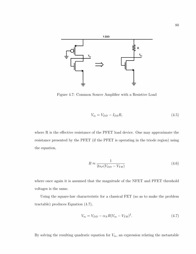
80
Figure 4.7: Common Source Amplifier with a Resistive Load
Vm = VDD − IDSR, (4.5)
where R is the effective resistance of the PFET load device. One may approximate the
resistance presented by the PFET (if the PFET is operating in the triode region) using
the equation,
R ≈ 1
2αP (VDD − VTH)(4.6)
where once again it is assumed that the magnitude of the NFET and PFET threshold
voltages is the same.
Using the square-law characteristic for a classical FET (so as to make the problem
tractable) produces Equation (4.7),
Vm = VDD − αNR(Vm − VTH)2. (4.7)
By solving the resulting quadratic equation for Vm, an expression relating the metastable

81
voltage, Vm, to the supply voltage, VDD, can be found. The surprisingly simple result is
Vm = VTH
[1 +
1−√
1 + 2r
r
]+ VDD
[−1 +
√1 + 2r
r
]=
2
3VTH +
1
3VDD.
(4.8)
where r = αNαP
. For the design presented in this chapter, the value of r is 12. Applying the
techniques from Chapter 2 it is possible to show that
SτVDD =−VDD
VDD − VTH(4.9)
When comparing Equation (4.9) to Equation (4.3) one concludes that the circuit
discussed presented in Chapter 4 is less sensitive to changes in supply voltage than the
synchronizer of Chapter 3. If high-field effects associated with the NFET, are included
then
SτVDD =−VDD
VDD − VTHf(β) (4.10)
This equation will now be used to predict how τ will vary as the supply voltage is
swept from 0.8 V to 1.2 V which can then be compared with simulation results from
MetaACE.
4.7 Dependence of τ on Supply Voltage
After design verification, the circuit is ready to be used with MetaACE to verify
the sensitivity equations’ ability to predict trends in τ based upon changes in a given
parameter. This section will focus on the sensitivity of the specialized cell to changes in
supply voltage. The same conditions used in Section 3.6 are used for simulations in this
section.

82
Unlike Section 3.6, this will focus only on the Slave loop τ . The reason is that due to
simulation difficulties, the Master loop values could not be reliably measured. In theory,
this is inconsequential as the Master and Slave loops are identical and will thus have the
same value of τ . A VTL design will only be considered in this section because there is no
new information to be gained by analyzing devices with other threshold voltages.
VDD (V) Simulated Predicted
0.8 to 0.9 10% 11%
0.9 to 1.0 6% 9%
1.0 to 1.1 3% 8%
1.1 to 1.2 3% 6%
Table 4.3: Percentage Decrease in τ for Changing Supply Voltages
The sensitivity of the simulated τ to the supply voltage is worth exploring before
comparing the predicted values of τ to the values obtained from MetaACE. Table 4.3
gives the percentage change in τ for increasing supply voltage by increments of 100 mV.
Unsurprisingly, the sensitivity of the Chapter 4 circuit is less than that of the Chapter
3 circuit. The correlation coefficient for simulated and predicted data in Figure 4.8 is
0.9853.
While supply voltage is less sensitive in comparison to Chapter 3, an important
distinction must be reiterated. The circuit simulated in Chapter 3 was an extracted netlist
containing parasitic capacitances, while the Chapter 4 circuit contained no information
concerning parastic elements. Due to the inability to simulate an extracted netlist for
Chapter 4, the actual level of improvement might be less significant. The difference
between a simulated τ for a schematic design and an extracted layout is beyond the scope
of this thesis and as such, it will not be examined in this work.

83
Figure 4.8: Predicted vs. Simulated τ for VTL Slave Loop
4.8 Variability of the Metastability Voltage
In Section 2.11 it was stated that one method of making a synchronizer tolerant to
process variation was to pick a topology with a metastable voltage which was less sensitive
to variation of parameters. The metastable voltage can guarantee operation in the strong
inversion regime with some important restrictions. The first restriction, also mentioned
in Section 2.11, is that the devices must be made no wider than necessary to obtain the
optimum value of τ . The second restriction is that the threshold voltage must be less
than the metastable voltage.
The sensitivity of Vm to VDD shown in Figure 4.9 illustrates that the Chapter 4
circuit indeed has a lesser slope. At lower supply voltages, a higher Vm was obtained for
the specialized synchronizer cell which is the ideal scenario, and why at lower supplies in
Section 4.7, the sensitivity analysis did a better job at predicting τ .
To give a quantitative measure of the sensitivity, a slope was calculated for each of
the graphs at the extremes of the supply range. The general flip-flop from Chapter 3 has
a slope of 0.5 V/V while the specialized synchronizer has a slope of only 0.35 V/V, a 30%
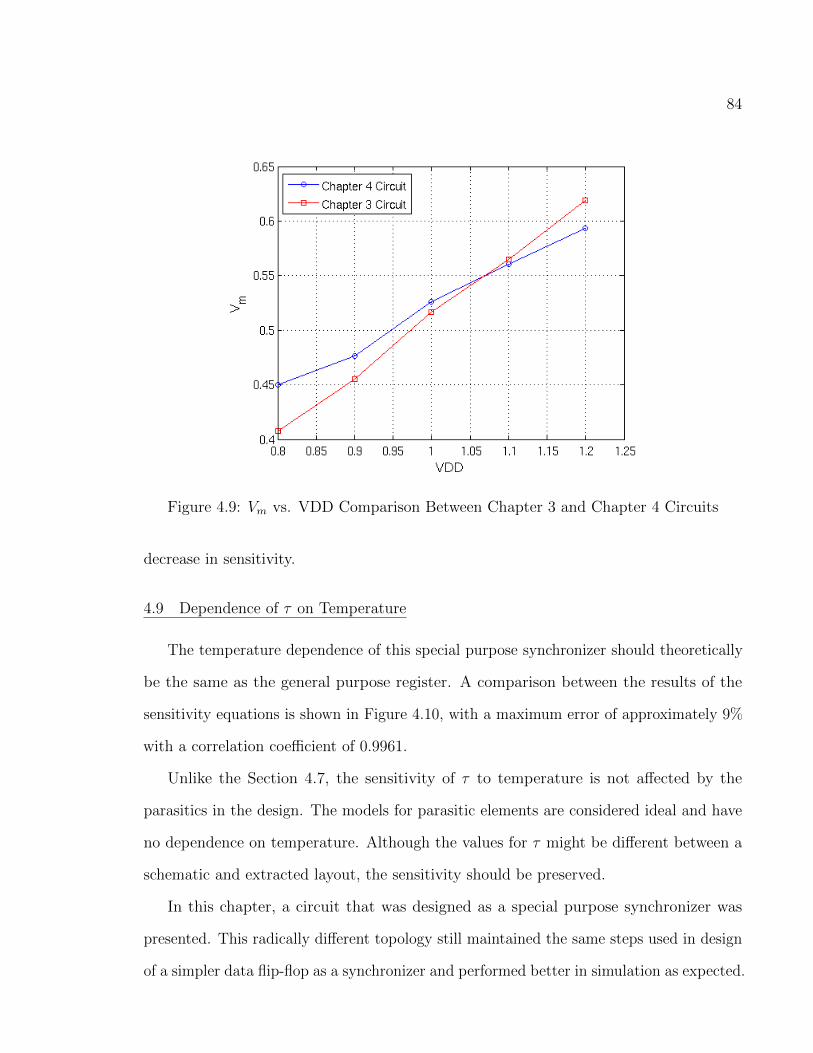
84
Figure 4.9: Vm vs. VDD Comparison Between Chapter 3 and Chapter 4 Circuits
decrease in sensitivity.
4.9 Dependence of τ on Temperature
The temperature dependence of this special purpose synchronizer should theoretically
be the same as the general purpose register. A comparison between the results of the
sensitivity equations is shown in Figure 4.10, with a maximum error of approximately 9%
with a correlation coefficient of 0.9961.
Unlike the Section 4.7, the sensitivity of τ to temperature is not affected by the
parasitics in the design. The models for parasitic elements are considered ideal and have
no dependence on temperature. Although the values for τ might be different between a
schematic and extracted layout, the sensitivity should be preserved.
In this chapter, a circuit that was designed as a special purpose synchronizer was
presented. This radically different topology still maintained the same steps used in design
of a simpler data flip-flop as a synchronizer and performed better in simulation as expected.

85
Figure 4.10: Predicted vs. Simulated τ for VTL Slave Loop in the Automotive Temperature
Range
Physical layouts were generated, but extracted netlists were not used with MetaACE due
to difficulties with the tools.
The sensitivity equations had to be slightly modified in this section due to the
different design style employed. Regardless of modifications, the resulting equations were
surprisingly similar. The main difference between the analysis in this chapter and Chapter
3 was the elimination of a section on threshold voltage. This was instead replaced by
a small section on the sensitivity of the metastable voltage to the supply voltage. This
provided a fundamental reason why this specialized synchronizer performed better than a
general flip-flop. As in Chapter 3, the predicted data was found to be highly correlated
with the simulated data, thus cementing the robustness of sensitivity analysis.

86
CHAPTER 5
SUMMARY, CONCLUSIONS, AND FUTURE WORK
In this thesis, the impact of PVT variations on synchronizer parameters is explored. This
topic is of vital importance due to the increasing variation caused by aggressive scaling
driven by Moore’s Law. This chapter will give a summary of the contributions made by
this work as well intended future work.
5.1 Sensitivity Analysis
The characteristics of metastability were thoroughly discussed so that the mathematical
framework to follow has a basis. The parameters τ and TW were examined and determined
to be the key to describing a flip-flop in metastability. A model of a standard flip-flop in
metastability was presented and analyzed in detail to show how these parameters may be
determined. τ was determined the dominant parameter used in the MTBF equation.
The I-V characteristics of MOSFETs in the strong and weak inversion regimes were
discussed alongside equations to provide an understanding of the possible behavior of
devices in a synchronizer design. An introduction to formal sensitivity analysis gave
the reader an overview of how the equations and methods described in the thesis were
formulated. This was then applied to find sensitivity equations for the dominant parameter
τ . The benefit of this analysis was the ability to quickly determine the value of τ for some
other operating point which could include changes in temperature, process, or supply
voltages.
In the development of an expression for sensitivity to supply voltage, the expressions
were found to be quite simple. A sensitivity factor was developed for strongly and weakly
inverted devices to make a complete model. The equations showed that to decrease the
overall value and variability of τ , strongly inverted devices were highly preferable. It was
87
also found that one can reduce variability of τ by selecting a topology with a metastable
voltage which varies as little as possible.
A sensitivity factor was developed for the threshold voltage in much the same manner
as for supply voltage. Factors for both the strongly and weakly inverted cases were seen
to be quite simple. They showed that to reduce sensitivity, the threshold voltage will
ideally be as small as possible.
The final sensitivity factor formulated was for temperature. Sensitivity factors relating
to mobility and threshold voltage were developed and used through the chain rule with
sensitivity factors for τ based upon threshold and mobility. The chapter concluded with
an algorithm for determining τ from a single known value and suggested methods for
PVT tolerant designs.
5.2 A Standard Flip-Flop Synchronizer Case Study
A standard flip-flop topology was chosen as the first case study in this work because
of its simplicity as well as widespread use in the semiconductor industry. An overall
description of the circuit was given. The details of design choices such as including Design
for Testability (DFT) circuitry were briefly discussed as well.
The relation of gain-bandwidth product (GBW) to τ was presented and utilized as
a motivating factor in the design. This metric was shown to be useful in the sizing of
transistors in the following section. To size the devices, an analog testbench was developed
and simulated with only transistors. Simulation with additional capacitance on critical
nodes was done to find values for GBW more indicative of a design with real wires.
A discussion of physical layout of the cell was necessary to allow the reader to be able
to replicate work done. The standard cell sizing rules used as well as a brief description
of layout verification and netlist generation were given. A section on the performance
of the design based upon setup, hold and clock-to-Q times were given to show how the
design might perform outside of metastability.
88
The results from MetaACE and the sensitivity equations developed in Chapter 2 were
covered in the final sections of the chapter. It was found that the error in the sensitivity
analysis was very small. It was verified that higher supply voltages and lower threshold
loop devices were the best options to produce a PVT tolerant synchronizer design.
5.3 A Specialized Synchronizer Case Study
The sensitivity analysis method proposed in Chapter 2 was incredibly accurate for a
simple design, but it was important that this method transcend topology since it only
relies on device physics and basic models. To this end, a widely different circuit was
discussed.
The first major difference between the specialized synchronizer and the flip-flop
presented in Chapter 3 was the latch used. A pseudo-NMOS latch proposed by Ian Jones
at Oracle R© was chosen due to some unique properties it has. One key benefit of this
circuit is that as a practical design, it has very little capacitance on the metastable node,
therefore affording it a better value of τ over some other designs. The other important
property is that because of the resistive loading for the NMOS devices, it will experience
less sensitivity to supply variation. Aside from a different latch, the differences in the
flip-flop topology were discussed to give an idea of how the circuit works. A scan-chain
version of this synchronizer was created as well.
The specialized cell was run through the same type of tests as those performed in
Chapter 3. Although the topology was very different, only a few things about the tests
changed. The small signal equivalent circuit used to model the regenerative loops was
changed to the type of loop devices used in the specialized cell. The small signal analysis
results yielded a higher GBW (lower τ) for the plain testbench, as well as the testbench
with parasitic capacitors added on critical nodes.
Circuit layout was done with the hopes of generating a netlist with parasitics, but
the netlist generated had many problems in the HSPICE Format. Because MetaACE

89
does not currently support Spectre R© the extracted cell was only used for verification of
operational parameters.
The schematic version of the circuit was run through MetaACE to generate results for
sensitivity analysis involving supply and temperature variations. Sensitivity to threshold
voltage was determined unnecessary and thus omitted.
A section discussing the need for modification of the sensitivity equations for supply
voltage was necessary. While the sensitivity factors developed were similar, there was
need for correction due to the non-complementary nature of the inverters used.
A small discussion was presented on the differences in results for supply variation
from that of the general flip-flop. Most notably, the specialized synchronizer τ showed
significantly less variation to that of the general synchronizer cell. The results found in
supply sensitivity for the specialized synchronizer cell were accurate once again thanks to
the small modifications made to the sensitivity factors.
A comparison was made between the metastability voltage for the general flip-flop
versus the specialized synchronizer was discussed. The metastable voltage for the gen-
eral flip-flop was always approximately half of the supply voltage, but the specialized
synchronizer circuit was less sensitive changing at only 0.35 V/V.
In comparing the results of these two radically different circuits, the sensitivity
equations are quite accurate. The capability of sensitivity analysis was verified and
showed that the behavior of two vastly different designs can be predicted in the presence
of PVT variations through simple equations.
5.4 Future Work
In the world of research there is always more to do, and that holds particularly true for
this thesis. The following list gives a brief view of the work that still lies ahead regarding
this thesis:
• Simulation at worst case corners

90
• Simulation of multistage synchronizers in the presence of process variability
• Comparison of results between a schematic version of Chapters 3 and 4 circuits
• Comparison of results between an extracted version of Chapters 3 and 4 circuits
• Development of sensitivity equations for moderate inversion
• Fabrication of the circuits described in this thesis using a real process and verification
in a real world setting
91
REFERENCES
[Altera, 2014] Altera (1995-2014). Enhanced temperature device support. http://www.altera.com/devices/common/ind/ind-temp.html#notes. Accessed: 2014-06-25.
[Bassett et al., 1990] Bassett, R., Turner, M. E., Panner, J., Gillis, P., Oakland, S., andStout, D. (1990). Boundary-scan design principles for efficient lssd asic testing.IBM Journal of Research and Development, 34(2.3):339–354.
[Beer et al., 2014] Beer, S., Cox, J., and Ginosar, R. (2014). Variability of multistagesyncrhonizers. to appear.
[Beer et al., 2013] Beer, S., Ginosar, R., Dobkin, R., and Weizman, Y. (2013). Mtbfestimation in coherent clock domains. In Asynchronous Circuits and Systems(ASYNC), 2013 IEEE 19th International Symposium on, pages 166–173.
[Chaney and Molnar, 1973] Chaney, T. and Molnar, C. (1973). Anomalous behavior ofsynchronizer and arbiter circuits. Computers, IEEE Transactions on, C-22(4):421–422.
[Cox, 2014] Cox, J. (2014). Personal Conversations.
[Ginosar, 2011] Ginosar, R. (2011). Metastability and synchronizers: A tutorial. DesignTest of Computers, IEEE, 28(5):23–35.
[Iordache et al., 2008] Iordache, M., Dumitriu, L., and Niculae, D. (2008). On thesensitivity analysis of analog circuits. Annals of the University of Craiova, ElectricalEngineering series, (32):11–16.
[ITRS, 2012] ITRS (2012). Test and test equipment. http://www.itrs.net/Links/
2012Winter/1205%20Presentation/Test_12052012.pdf. accessed : 2014-06-14.
[Jones, 2013] Jones, I. (2013). Personal Conversations.
[Jones et al., 2013] Jones, I., Suwen, Y., Greenstreet, M., Gaywala, H., and Drost, R.(2013). Synchronizer latch circuit that facilitates resolving metastability.
[Katz, 2005] Katz, R. (2005). Contemporary logic design. Pearson Prentice Hall, UpperSaddle River, N.J.
[Li, 2011] Li, D. (2011). Design and Analysis of Metastable-Hardened, High-Performance,Low-Power Flip Flops. PhD thesis, University of Waterloo, Waterloo, Ontario,Canada.
[Rabaey, 2003] Rabaey, J. (2003). Digital integrated circuits : a design perspective.Pearson Education, Upper Saddle River, N.J.

92
[Razavi, 2001] Razavi, B. (2001). Design of analog CMOS integrated circuits. McGraw-Hill, Boston, MA.
[Saonwani et al., 2012] Saonwani, M., Khanna, G., and Chandel, R. (2012). Impact ofprocess variability on universal gates. In Signal Processing, Computing and Control(ISPCC), 2012 IEEE International Conference on, pages 1–6.
[Tsividis, 2011] Tsividis, Y. (2011). Operation and modeling of the MOS transistor.Oxford University Press, New York.
[Veendrick, 1980] Veendrick, H. J. M. (1980). The behaviour of flip-flops used as synchro-nizers and prediction of their failure rate. Solid-State Circuits, IEEE Journal of,15(2):169–176.
[Weste, 2006] Weste, N. (2006). CMOS VLSI design : a circuits and systems perspective.Pearson Education, Delhi.
[Wolpert, 2012] Wolpert, D. (2012). Managing temperature effects in nanoscale adaptivesystems. Springer, New York.
[Yang et al., 2011] Yang, S., Jones, I., and Greenstreet, M. (2011). Synchronizer per-formance in deep sub-micron technology. In Asynchronous Circuits and Systems(ASYNC), 2011 17th IEEE International Symposium on, pages 33–42.
93
APPENDIX
TCL Script
#!/ usr / b in / t c l s h
#
# Csv package from t c l l i b a l l o w s us to work wi th csv f i l e s
#
package require csv
package require s t r u c t : : m a t r i x
# Filenamve o f CSV f i l e we want to read
# Read the f i l e name from the command l i n e
# Expect ing e x a c t l y one commant l i n e argument
i f { $argc == 1} {
set r e a d f i l e n a m e [ lindex $argv 0 ]
set w r i t e f i l e n a m e $ r e a d f i l e n a m e
# puts $ r e a d f i l e n a m e
# puts $w r i t e f i l e n a m e
} else {
puts ” Usage: vdd f i l ename ”
exit

94
}
#
# Tcl code to p r e d i c t change in tau in response to change
# in supp ly v o l t a g e
# Supply a Vdd increment , t h r e s h o l d v a l u e , and be ta v a l u e
# Beta accounts f o r sma l l channel e f f e c t s
#
set de l ta vdd 0 .001
# S e t t i n g be ta e q u a l to 0 removes h i g h− f i e l d e f f e c t s
# Reading v a l u e s from UNIX environment v a r i a b l e s
set beta $env (BETA)
set vth $env (VTH)
# ∗∗∗∗∗∗∗∗∗∗∗∗∗∗∗∗∗∗∗∗∗∗∗∗∗∗∗∗∗∗∗∗∗∗∗∗∗∗∗∗∗∗∗∗∗∗∗∗∗∗∗∗∗∗∗∗∗∗∗∗∗∗
# Procedure to p r e d i c t new tau v a l u e from known tau v a l u e
# This v e r s i o n even has c o r r e c t i o n s f o r sma l l channel e f f e c t s
# Assumption i s t h a t m e t a s t a b l e v o l t a g e i s 1/2 o f supp ly v o l t a g e
#

95
proc p r e d i c t t a u { o ld tau vth beta vdd de l ta vdd } {
set tmp [ expr { ( $vdd / 2 . 0 ) − $vth } ]
set s e n s i t i v i t y [ expr { −( $vdd / 2 . 0 ) / $tmp } ]
set smal l chan [ expr { 2 . 0 / (2 . 0 + (3 .0∗$beta∗$tmp )
+ $beta∗$beta∗$tmp∗$tmp ) } ]
set s e n s i t i v i t y [ expr { $smal l chan ∗ $ s e n s i t i v i t y } ]
set tmp [ expr { 1 + $ s e n s i t i v i t y ∗ ( $de l ta vdd /$vdd ) } ]
set new tau [ expr { $tmp ∗ $o ld tau } ]
return $new tau
}
# ∗∗∗∗∗∗∗∗∗∗∗∗∗∗∗∗∗∗∗∗∗∗∗∗∗∗∗∗∗∗∗∗∗∗∗∗∗∗∗∗
#
# Procedure to r e v e r s e a Tcl l i s t
i f { [ info command l r e v e r s e ] == ””} {
proc l r e v e r s e l i s t {
set r e s {}
set i [ llength $ l i s t ]
while { $ i } {

96
lappend r e s [ lindex $ l i s t [ incr i −1 ] ]
}
set r e s
}
}
# ∗∗∗∗∗∗∗∗∗∗∗∗∗∗∗∗∗∗∗∗∗∗∗∗∗∗∗∗∗∗∗∗∗∗∗∗∗∗∗∗∗∗∗∗∗∗∗
#
# Read the csv f i l e i n t o a matrix
#
# CSV f i l e from MetaACE to read
: : s t r u c t : : m a t r i x data
set chan [open ” . /metaACE/ $ r e a d f i l e n a m e ” ” r ” ]
c sv : : r e a d 2m at r i x $chan data , auto
close $chan
# Determine the number o f rows in matrix
set rows [ data rows ]
# Grab the vdd and ytau v a l u e s from the MetaACE f i l e

97
# Vdd v a l u e s must have a uniform format i . e . the use
# of the format command
# Create a p a i r o f l i s t s
set vdd values {}
set t au va lue s {}
for { set row 1} {$row < $rows} { incr row} {
set vdd [ data get c e l l 0 $row ]
set vdd [ format %. 1 f $vdd ]
set ytau [ format %. 1 f [ data get c e l l 7 $row ] ]
lappend vdd values $vdd
lappend t au va lue s $ytau
}
puts ””
puts ”Reading $ r e a d f i l e n a m e . . . ”
puts ”Vdd va lue s r ead : ”
puts $vdd values
puts ” Corresponding ytau va lues read . . . ”
puts $tau va lue s

98
# Assume vdd v a l u e s i n c r e a s i n g
set i n i t i a l v d d [ lindex $vdd values 0 ]
set f i n a l v d d [ lindex $vdd values end ]
# Construct a g r i d o f vdd v a l u e s on which we would
# l i k e to p r e d i c t taus
# The vdd v a l u e s are s t o r e d as a l i s t c a l l e d v d d g r i d
set vdd gr id {}
set eps 1e−4
# ” f o r ” loop i s a d j u s t e d to f i t on page , i f copying t h i s code
# f i x f o r m a t t i n g by p u t t i n g l i n e r i g h t be low ” f o r ” on the same
# l i n e
for { set vdd $ i n i t i a l v d d } {$vdd <= $ f i n a l v d d + $eps}
{ set vdd [ expr {$vdd + $de l ta vdd } ]} {
lappend vdd gr id $vdd
}
# Find middle index
# Best i f whe i t e r a t e in both d i r e c t i o n s , s t a r t i n g in the middle

99
# S p l i t the g r i d up i n t o an ” upper ” and a ” lower ” g r i d
set l i s t l e n g t h [ llength $vdd gr id ]
set mid [ expr { $ l i s t l e n g t h / 2 } ]
set upper gr id [ lrange $vdd gr id $mid end ]
set l o w e r g r i d [ lrange $vdd gr id 0 [ expr $mid−1 ] ]
# Construct a l i s t o f tau v a l u e s based on
# the g r i d o f vdd v o l t a g e s
# This time the g r i d o f tau v a l u e s w i l l
# be s t o r e d as an a s s o c i a t i v e array
set l i s t l e n g t h [ llength $tau va lue s ]
set mid [ expr { $ l i s t l e n g t h / 2 } ]
set o ld tau [ lindex $tau va lue s $mid ]
# Work on the upper h a l f o f the curve
foreach vdd $upper gr id {
set t a u g r i d ( $vdd ) [ format %. 1 f $o ld tau ]
set new tau p r e d i c t t a u $o ld tau $vth $beta $vdd $de l ta vdd ]
set o ld tau $new tau

100
}
# Now work on the lower h a l f o f the curve
# Need to r e v e r s e the order o f v a l u e s in l o w e r g r i d l i s t
set de l ta vdd [ expr { −1 ∗ $de l ta vdd } ]
set o ld tau [ lindex $tau va lue s $mid ]
set l o w e r g r i d [ l r e v e r s e $ l o w e r g r i d ]
foreach vdd $ l o w e r g r i d {
set t a u g r i d ( $vdd ) [ format %. 1 f $o ld tau ]
set new tau [ p r e d i c t t a u $o ld tau $vth $beta $vdd $de l ta vdd ]
set o ld tau $new tau
}
# Write a f i l e c o n t a i n i n g vdd , a c t u a l t a u , p r e d i c t e d tau
puts ” Creat ing $ w r i t e f i l e n a m e . . . ”
set f i d [open ” . /matlab/ $ w r i t e f i l e n a m e ” ”w” ]
puts $ f i d ” Vdd,Ytau,Predict ion ”
foreach vdd $vdd values tau $tau va lue s {
puts $ f i d ” $vdd , $ tau , $ tau g r id ( $vdd ) ”

101
}
close $ f i d
puts ” S u c c e s s f u l . . . e x i t i n g ! ”
puts ””