Data Exchange - 0312 - Ansertekansertek.com/uploads/3/3/9/4/3394509/odb_data_export.pdf ·...
94
TRILOGY / ENTERPRISE Data Exchange DATA EXCHANGE Version 5.2 Document 0312.1007 Published October 2007 © 2007 Valor Computerized Systems, Ltd. All rights reserved. This document contains proprietary information belonging to Valor Computerized Systems, Ltd. This information is not for publication and is issued on condition that it will not be copied, printed or disclosed to a third party, without the written consent of Valor Ltd. This document is subject to change without notice. Valor Computerized Systems, Ltd., 4 Faran Road P.O.Box 152, Yavne Industrial Area 70600 Yavne, ISRAEL Voice: 972-8-943-2430 Fax: 972-8-943-2429 Web site: http://www.valor.com Documentation email: [email protected]
-
Upload
nguyenkhanh -
Category
Documents
-
view
213 -
download
0
Transcript of Data Exchange - 0312 - Ansertekansertek.com/uploads/3/3/9/4/3394509/odb_data_export.pdf ·...
TRILOGY / ENTERPRISEData Exchange
DATA EXCHANGEVersion 5.2
Document 0312.1007Published October 2007
© 2007 Valor Computerized Systems, Ltd.All rights reserved.
This document contains proprietary information belonging to ValorComputerized Systems, Ltd. This information is not for publicationand is issued on condition that it will not be copied, printed ordisclosed to a third party, without the written consent of Valor Ltd.This document is subject to change without notice.
Valor Computerized Systems, Ltd.,4 Faran Road
P.O.Box 152, Yavne Industrial Area70600 Yavne, ISRAELVoice: 972-8-943-2430Fax: 972-8-943-2429
Web site: http://www.valor.comDocumentation email: [email protected]

Table of Contents
Chapter 1 OverviewODB++ Description . . . . . . . . . . . . . . . . . . . . . . . . . . . . . . . . . . . . . . . . 5Intended Readers . . . . . . . . . . . . . . . . . . . . . . . . . . . . . . . . . . . . . . . . . . . 6
Chapter 2 Getting StartedSupported CAD Tools . . . . . . . . . . . . . . . . . . . . . . . . . . . . . . . . . . . . . . 7Displaying the ODB++ Design in the VUV . . . . . . . . . . . . . . . . . . . . 8Exporting to an ODB++(X) File . . . . . . . . . . . . . . . . . . . . . . . . . . . . . . 9
Defining ODB++(X) Settings . . . . . . . . . . . . . . . . . . . . . . . . . . . . . . . 9Table of Export Levels for FAB and ASSY Modes . . . . . . . . . . . . . 11
Chapter 3 CadenceAllegro . . . . . . . . . . . . . . . . . . . . . . . . . . . . . . . . . . . . . . . . . . . . . . . . . . 12
Allegro Database . . . . . . . . . . . . . . . . . . . . . . . . . . . . . . . . . . . . . . . . 12Creating ODB++ Output . . . . . . . . . . . . . . . . . . . . . . . . . . . . . . . . . . 13Specifying File Options and Output Options . . . . . . . . . . . . . . . . . . . 16Specifying Parameters Specific to Cadence Allegro . . . . . . . . . . . . . 17Editing the Matrix File . . . . . . . . . . . . . . . . . . . . . . . . . . . . . . . . . . . . 20Suppressing Unconnected Pads . . . . . . . . . . . . . . . . . . . . . . . . . . . . . 22Cadence Allegro Extraction Files . . . . . . . . . . . . . . . . . . . . . . . . . . . 23Specifying Positive ANTI ETCH Surfaces . . . . . . . . . . . . . . . . . . . . 26Placing Components Underneath Raised Components . . . . . . . . . . . 26Using Height Parameters for Keepout Areas . . . . . . . . . . . . . . . . . . . 27Deleting Temporary Sort Pins Files . . . . . . . . . . . . . . . . . . . . . . . . . . 28Sorting the Pins File Numerically with Numeric Pins Last . . . . . . . . 29Specifying an Alternate Font File . . . . . . . . . . . . . . . . . . . . . . . . . . . 29Controlling Handling of Invalid Attributes . . . . . . . . . . . . . . . . . . . . 29Exporting Partial ODB++ Data . . . . . . . . . . . . . . . . . . . . . . . . . . . . . 29
Orcad-Layout . . . . . . . . . . . . . . . . . . . . . . . . . . . . . . . . . . . . . . . . . . . . . 32Orcad-Layout Database . . . . . . . . . . . . . . . . . . . . . . . . . . . . . . . . . . . 32Creating ODB++ Output . . . . . . . . . . . . . . . . . . . . . . . . . . . . . . . . . . 32
0312.1007 Data Exchange 2

Chapter 4 Mentor GraphicsBoard Station . . . . . . . . . . . . . . . . . . . . . . . . . . . . . . . . . . . . . . . . . . . . . 34
Board Station Database . . . . . . . . . . . . . . . . . . . . . . . . . . . . . . . . . . . 34Relevant Files . . . . . . . . . . . . . . . . . . . . . . . . . . . . . . . . . . . . . . . . . . . 35Post Processing Options . . . . . . . . . . . . . . . . . . . . . . . . . . . . . . . . . . . 39Creating ODB++ Output . . . . . . . . . . . . . . . . . . . . . . . . . . . . . . . . . . 40Specifying File Options and Output Options . . . . . . . . . . . . . . . . . . . 42Specifying Parameters Specific to Mentor Board Station . . . . . . . . . 43Support for Embedded Passive Components . . . . . . . . . . . . . . . . . . . 46Controlling Handling of Invalid Attributes . . . . . . . . . . . . . . . . . . . . 46Controlling the Algorithm Used to Delete Unused Pads . . . . . . . . . . 47Assigning Clearance Areas by Drill Center or Area . . . . . . . . . . . . . 47
PowerPCB (PADS) . . . . . . . . . . . . . . . . . . . . . . . . . . . . . . . . . . . . . . . . 48Defining CAM Documents . . . . . . . . . . . . . . . . . . . . . . . . . . . . . . . . 48Filling Copper Pour Outlines . . . . . . . . . . . . . . . . . . . . . . . . . . . . . . . 49Saving Split/Mixed Plane Data . . . . . . . . . . . . . . . . . . . . . . . . . . . . . 51Creating the ASCII File . . . . . . . . . . . . . . . . . . . . . . . . . . . . . . . . . . . 52
Expedition . . . . . . . . . . . . . . . . . . . . . . . . . . . . . . . . . . . . . . . . . . . . . . . 53Creating ODB++ Output . . . . . . . . . . . . . . . . . . . . . . . . . . . . . . . . . . 53
Supermax ECAD . . . . . . . . . . . . . . . . . . . . . . . . . . . . . . . . . . . . . . . . . . 55Creating ODB++ Output from the CAM Output Dialog Box . . . . . . 55Creating ODB++ Output from the File > Export Option . . . . . . . . . . 55Output - Mapfile . . . . . . . . . . . . . . . . . . . . . . . . . . . . . . . . . . . . . . . . . 56
Chapter 5 ZukenVisula . . . . . . . . . . . . . . . . . . . . . . . . . . . . . . . . . . . . . . . . . . . . . . . . . . . 58
Creating ODB++ Output from the Visula Interface Menu . . . . . . . . 58Creating ODB++ or ODB++(X) using a Standalone Program . . . . . 59Specifying File Options and Output Options . . . . . . . . . . . . . . . . . . . 61Specifying Parameters Specific to Zuken Visula . . . . . . . . . . . . . . . . 62Exporting Partial ODB++ Data . . . . . . . . . . . . . . . . . . . . . . . . . . . . . 64
Board Designer (CR5000) . . . . . . . . . . . . . . . . . . . . . . . . . . . . . . . . . . 67Zuken BD Database . . . . . . . . . . . . . . . . . . . . . . . . . . . . . . . . . . . . . . 67Generating ASCII Files . . . . . . . . . . . . . . . . . . . . . . . . . . . . . . . . . . . 67
PWS (CR3000) . . . . . . . . . . . . . . . . . . . . . . . . . . . . . . . . . . . . . . . . . . . 69Zuken PWS Database . . . . . . . . . . . . . . . . . . . . . . . . . . . . . . . . . . . . . 69
Cadstar . . . . . . . . . . . . . . . . . . . . . . . . . . . . . . . . . . . . . . . . . . . . . . . . . . 70Creating ODB++ Output . . . . . . . . . . . . . . . . . . . . . . . . . . . . . . . . . . 70
Chapter 6 AltiumDesigner (formerly Protel) . . . . . . . . . . . . . . . . . . . . . . . . . . . . . . . . . . 72
0312.1007 Data Exchange 3

Creating ODB++ Output Using Project Options . . . . . . . . . . . . . . . . 72Creating ODB++ Output Using the Output Job File Option . . . . . . . 75
P-CAD . . . . . . . . . . . . . . . . . . . . . . . . . . . . . . . . . . . . . . . . . . . . . . . . . . 81Creating ODB++ Output . . . . . . . . . . . . . . . . . . . . . . . . . . . . . . . . . . 82
Chapter 7 Number One SystemsEasy-PC for Windows . . . . . . . . . . . . . . . . . . . . . . . . . . . . . . . . . . . . . 84
Creating ODB++ Output . . . . . . . . . . . . . . . . . . . . . . . . . . . . . . . . . . 84
Chapter 8 PulsonixPulsonix . . . . . . . . . . . . . . . . . . . . . . . . . . . . . . . . . . . . . . . . . . . . . . . . . 85
Creating ODB++ Output . . . . . . . . . . . . . . . . . . . . . . . . . . . . . . . . . . 85
Chapter 9 VisionicsEDWinXP . . . . . . . . . . . . . . . . . . . . . . . . . . . . . . . . . . . . . . . . . . . . . . . . 87
Creating ODB++ Output . . . . . . . . . . . . . . . . . . . . . . . . . . . . . . . . . . 87
Chapter 10 ValorEnterprise 3000 . . . . . . . . . . . . . . . . . . . . . . . . . . . . . . . . . . . . . . . . . . . 88
Creating ODB++ Output . . . . . . . . . . . . . . . . . . . . . . . . . . . . . . . . . . 88Creating ODB++(X) Output . . . . . . . . . . . . . . . . . . . . . . . . . . . . . . . 89
Appendix A Thermal ModelStructure of a Thermal Model File . . . . . . . . . . . . . . . . . . . . . . . . . . . 91BNF (Backus-Naur Form) of Rules . . . . . . . . . . . . . . . . . . . . . . . . . . 91Sample Thermal Model File . . . . . . . . . . . . . . . . . . . . . . . . . . . . . . . . 92
0312.1007 Data Exchange 4

Chapter 1 Overview
This manual defines the requirements and procedures for translating PCB design data and producing ODB++ V7 files.
The ODB++ data format is a common language used for DFM and CAD/CAM data exchange. It overcomes data communication obstacles between design, manufacturing and assembly. Data in this powerful open database imparts an integrated and accurate physical model of all bareboard, component, and test-related information.
The Valor Universal Viewer (VUV), lets you view the ODB++ design data graphically on Windows, Sun Solaris, or HP-UX workstations. If the VUV is not
installed at your site, the VUV icon is not displayed. Contact Valor for information about the VUV.
ODB++ DescriptionODB++ is widely accepted as a practical de-facto standard within the electronics industry to efficiently move printed circuit bare-board, assembly and test data on the manufacturing-engineering level within design/manufacturing supply chains. It is a simple yet comprehensive description of all entities needed in the manufacture of a printed circuit board. Originally defined by Valor, ODB++ is now in common use by third-party tool providers within the industry. Valor is committed to a policy of supporting organizations wishing to implement the ODB++ format.
ODB++ ODB++ uses a standard file system structure. A job in ODB++ is represented by a stand-alone directory tree that can be transferred between systems without loss of data. The advantages of a directory tree compared to one large file are apparent when a job is being read from disk or saved to disk. The flexible tree structure allows a selected part of the job to be read/saved, avoiding the overhead of reading and writing a large file. When a job tree must be transferred to another system, standard compression utilities can be used to convert a directory tree into a single file.
ODB++ (X) ODB++(X), based on XML, was developed to simplify the data transfer between design and manufacturing. Based on the information stored in ODB++ and coupled with the needs expressed by users, ODB++(X) extensively covers all aspects of a manufacturing job. By using XML as the definition language, ODB++(X) allows developers to use off-the-shelf tools to read and process ODB++ jobs. These files have extension .xml.
0312.1007 Last Update: October 22, 2007 10:28 am Data Exchange 5
Chapter 1 OverviewIntended Readers
Intended ReadersThis manual is intended for users of PCB CAD design systems that are responsible for preparing and submitting designs to manufacturing departments (either in-house or sub-contract) that use Valor software tools.
It is assumed that the reader is familiar with the PCB Design tools and their output procedures.
0312.1007 Data Exchange 6

Chapter 2 Getting StartedSupported CAD Tools
Chapter 2 Getting Started
This document provides instructions for preparing an optimized design package from your CAD environment.
• Supported CAD Tools
• Displaying the ODB++ Design in the VUV
• Exporting to an ODB++(X) File
Supported CAD ToolsThis document is divided into sections by CAD tool.
Vendor CAD tool Versions supported
Cadence AllegroOrcad-Layout
11.0 and higher6.4.2 and higher
Mentor Graphics
Board StationPowerPCB (PADS)ExpeditionSupermax ECAD
B2 and higher2.0 and higherWG20029.0 and higher
Zuken Visula Board Designer (CR5000)PWS (CR3000)Cadstar
CADExpert 3.5 (CADIF 4) and higher6.02 and higher12.0 and higherCadstar 6 (CADIF 4) and higher
Altium Designer (formerly Protel)P-CAD
2.2 (v12) and higher99SE & DXP (ascii v3 & 4)
Number One Systems
Easy-PC for Windows 8.0 and higher
Pulsonix Pulsonix 3.0 and higher
Visionics EDWinXP
Valor Enterprise 3000 All
0312.1007 Data Exchange 7

Chapter 2 Getting StartedDisplaying the ODB++ Design in the VUV
Displaying the ODB++ Design in the VUVThe generated ODB++ file can be viewed with the Valor Universal Viewer (VUV). The VUV can be downloaded from the Valor web site at http://www.valor.com
0312.1007 Data Exchange 8

Chapter 2 Getting StartedExporting to an ODB++(X) File
Exporting to an ODB++(X) FileSome formats allow you to export a job to an ODB++(X) file. Define the ODB++(X) settings as described here.
• Defining ODB++(X) Settings
• Table of Export Levels for FAB and ASSY Modes
Defining ODB++(X) SettingsIf you will be outputting to an ODB++(X) file, you can define ODB++(X) parameters.
To define ODB++(X) settings:
Select ODB++(X) on the ODB++ Inside dialog box and click Show ODB++(X) Settings. The XML Export Setting dialog box opens.
Export Mode There are three Export Modes:
FULL - All ODB++ job data is represented. Job layers exported to ODB++(X) are shaded green.
FAB - Only fabrication data is represented.
ASSY - Only assembly data is represented.
The Fabrication and Assembly modes have several levels of ODB++(X) output:
• Fabrication has 4 levels - 1 (maximum) to 4 (minimum).
• Assembly has 6 levels - 1 (maximum) to 6 (minimum).
See “Table of Export Levels for FAB and ASSY Modes” on page 11.
Layers Mode Default - Layers are output according to the table above.
All - All layers are output - overrides the default settings.
None - No layers are output - overrides the default settings.
0312.1007 Data Exchange 9

Chapter 2 Getting StartedExporting to an ODB++(X) File
Units Imperial (mils) - 1/1000 of an inch
Metric (mm) - millimeter
Set DefaultValues button
Resets XML Export Settings to these defaults:
Export Mode - ASSY
Level - 6
Layers Mode - Default
Job’s Layers that will be exported to XML format - - Components/Packages + logical nets - Outer Layer copper pads
0312.1007 Data Exchange 10
Chapter 2 Getting StartedExporting to an ODB++(X) File
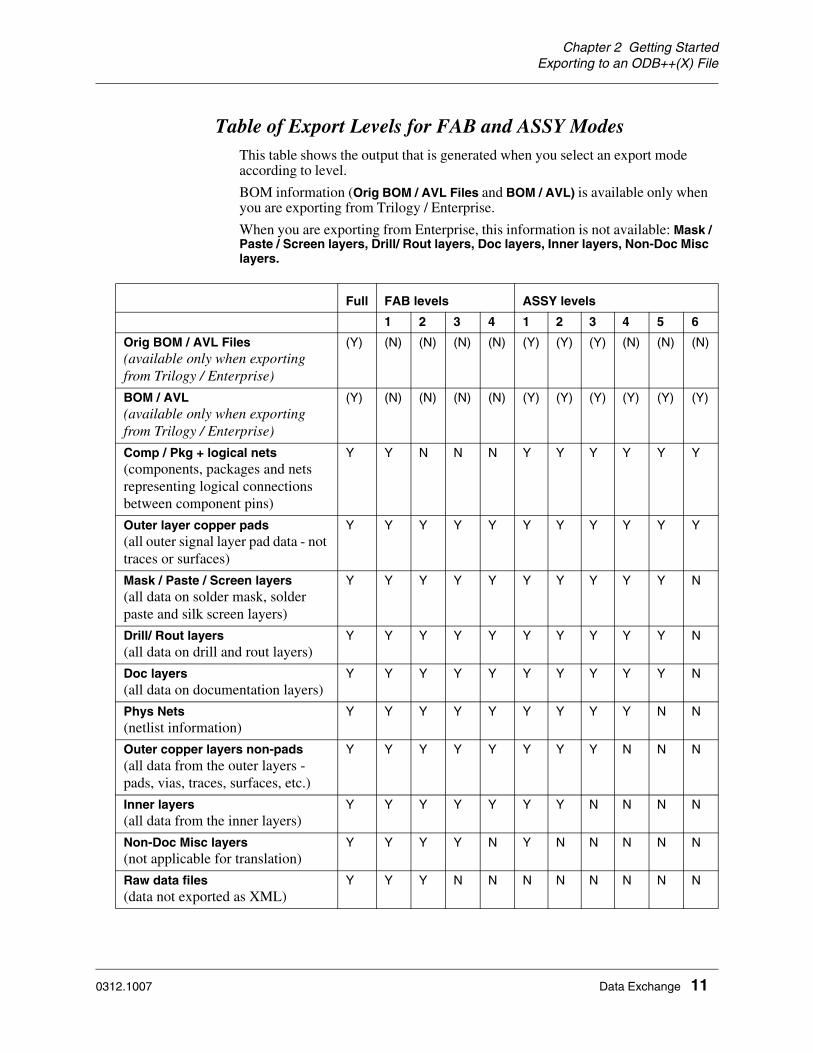
Table of Export Levels for FAB and ASSY ModesThis table shows the output that is generated when you select an export mode according to level.
BOM information (Orig BOM / AVL Files and BOM / AVL) is available only when you are exporting from Trilogy / Enterprise.
When you are exporting from Enterprise, this information is not available: Mask / Paste / Screen layers, Drill/ Rout layers, Doc layers, Inner layers, Non-Doc Misc layers.
Full FAB levels ASSY levels
1 2 3 4 1 2 3 4 5 6
Orig BOM / AVL Files(available only when exporting from Trilogy / Enterprise)
(Y) (N) (N) (N) (N) (Y) (Y) (Y) (N) (N) (N)
BOM / AVL(available only when exporting from Trilogy / Enterprise)
(Y) (N) (N) (N) (N) (Y) (Y) (Y) (Y) (Y) (Y)
Comp / Pkg + logical nets(components, packages and nets representing logical connections between component pins)
Y Y N N N Y Y Y Y Y Y
Outer layer copper pads(all outer signal layer pad data - not traces or surfaces)
Y Y Y Y Y Y Y Y Y Y Y
Mask / Paste / Screen layers(all data on solder mask, solder paste and silk screen layers)
Y Y Y Y Y Y Y Y Y Y N
Drill/ Rout layers(all data on drill and rout layers)
Y Y Y Y Y Y Y Y Y Y N
Doc layers(all data on documentation layers)
Y Y Y Y Y Y Y Y Y Y N
Phys Nets(netlist information)
Y Y Y Y Y Y Y Y Y N N
Outer copper layers non-pads(all data from the outer layers - pads, vias, traces, surfaces, etc.)
Y Y Y Y Y Y Y Y N N N
Inner layers(all data from the inner layers)
Y Y Y Y Y Y Y N N N N
Non-Doc Misc layers(not applicable for translation)
Y Y Y Y N Y N N N N N
Raw data files(data not exported as XML)
Y Y Y N N N N N N N N
0312.1007 Data Exchange 11

Chapter 3 CadenceAllegro
Chapter 3 Cadence
This chapter discusses the following formats:
• Allegro
• Orcad-Layout
AllegroIf you have Valor Enterprise 3000 installed, you can import Cadence Allegro files as described in Document 0303 Cadence Allegro Interface manual.
• Allegro Database
• Creating ODB++ Output
• Specifying File Options and Output Options
• Specifying Parameters Specific to Cadence Allegro
• Editing the Matrix File
• Suppressing Unconnected Pads
• Cadence Allegro Extraction Files
• Specifying Positive ANTI ETCH Surfaces
• Placing Components Underneath Raised Components
• Using Height Parameters for Keepout Areas
• Deleting Temporary Sort Pins Files
• Sorting the Pins File Numerically with Numeric Pins Last
• Specifying an Alternate Font File
• Controlling Handling of Invalid Attributes
• Exporting Partial ODB++ Data
Allegro DatabaseA Cadence Allegro design is saved in one binary file with the suffix brd, usually referred to as the brd file. The brd file is generally independent, with the exception of references to library symbols used for displaying thermal relief pads.
Inside the brd file, the data is organized in logical layers called subclasses. Each subclass belongs to a class that represents a particular type of data.
The following classes are included in the brd file:
0312.1007 Data Exchange 12

Chapter 3 CadenceAllegro
MostRelevant
etch - describes copper routes and planes
via class - describes via padstacks
pin - describes toeprint padstacks
package geometry - describes the physical components in the design board
geometry - describes the physical outline of the design
manufacturing - contains drill markers and various drawing data
ref des - contains component reference designators
LessRelevant
package keepinpackage keepoutanalysisanti etchcomponent valuedevice typedrawing formatdrc error classroute keepinroute keepouttoleranceuser part numbervia keepout
Creating ODB++ Output
Before generating ODB++ output, the Allegro film table must be completely defined so the physical layering and stackup of the PCB can be translated correctly.
The Allegro-to-ODB++ translator and the Valor Universal Viewer (VUV) for viewing ODB++ files, are contained within the ODB++ Inside suite that forms part of the Allegro installation.
The translator can be run on the following operating systems: HP-UX (11, 11i), Solaris (2.7, 8, 9, 10), Windows (2000, 2000 server, XP with SP2, Vista), Linux Red Hat 9, IBM-AIX (4.3).
To generate an ODB++ file:
1. Open the ODB++ Inside dialog box in one of these ways:
• Start the Allegro application and load a design. Click the ODB++ icon on the Allegro toolbar to display the ODB++ dialog.
0312.1007 Data Exchange 13

Chapter 3 CadenceAllegro
If the Valor Universal Viewer is not installed at your site, the VUV icon is not displayed. Contact Valor for information about the VUV.
If you do not have the ODB++ translator installed, a message is displayed:
• In Windows, select Start > Programs > Valor > ODB++ Inside or enter this command line: %ALLEGRO_BRD2ODB%/brd2odb.exe -gui.
• In UNIX, enter this command: $ALLEGRO_BRD2ODB/brd2odb -gui.
The ODB++ Inside dialog box opens.
0312.1007 Data Exchange 14

Chapter 3 CadenceAllegro
2. Specify basic options as described in “Specifying File Options and Output Options” on page 16.
3. If you will be outputting to an ODB++(X) file, select ODB++(X) and click Show ODB++(X) Settings to open the XML Export Setting dialog box and define ODB++(X) parameters. See “Defining ODB++(X) Settings” on page 9.
4. Click the Show Options icon to expand the ODB++ Inside dialog box to display tool-specific parameters. See “Specifying Parameters Specific to Cadence Allegro” on page 17.
5. To open the translator’s manual in PDF format, click the Help icon.
The configuration parameter gns_pdf_viewing_prog is set with the path and command to run a PDF viewer. For example: gns_pdf_viewing_prog=/sw/bin/acroread -useFrontEndProgram where /sw/bin/acroread is where the PDF viewer is stored.
6. To quit the translation program, click the Quit icon.
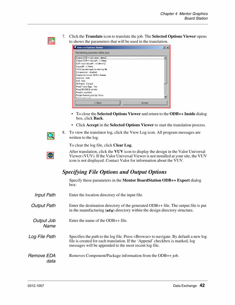
7. Click the Translate icon to translate the job. The Selected Options Viewer opens to shows the parameters that will be used in the translation.
• To close the Selected Options Viewer and return to the ODB++ Inside dialog box, click Back.
• Click Accept in the Selected Options Viewer to start the translation process.
8. To view the translator log, click the View Log icon. All program messages are written to the log.
0312.1007 Data Exchange 15

Chapter 3 CadenceAllegro
To clear the log file, click Clear Log.
After translation, click the VUV icon to display the design in the Valor Universal Viewer (VUV). If the Valor Universal Viewer is not installed at your site, the VUV icon is not displayed. Contact Valor for information about the VUV.
Specifying File Options and Output OptionsSpecify these parameters in the ODB++ Inside dialog box:
Input Path The directory of the input file. The default is the path to the current working directory.
Output Path The destination directory for the generated ODB++ file. The default is the path to the current working directory.
Output JobName
The name of the ODB++ file.
Log File Path The path to the log file.
Append If Append is selected, log messages will be appended to the most recent log file. By default a new log file is created for each translation.
Remove EDAdata
Component/Package information is not written to the ODB++ job.
NeutralizeNets
Nets are renamed numerically.
GZIP The ODB++ job is made up of several files describing the output. If GZIP is selected, compression creates a single tar and zip file. The default is not to compress.
PartialODB++
Export partial ODB++ output. See “Exporting Partial ODB++ Data” on page 29.
ODB++(X) ODB++(X) is a representation of the ODB++ format in XML. Select ODB++(X) to export in this format.
Export asODBV6
By default, information is exported in ODB++ Version 7 format. Select this option to export to the earlier ODB++ format.
ShowODB++(X)
Settings
The ODB++(X) interface lets you decide what data the ODB++(X) file will contain. Click Show ODB++(X) Settings to view/modify the export options. See “Defining ODB++(X) Settings” on page 9.
0312.1007 Data Exchange 16

Chapter 3 CadenceAllegro
Specifying Parameters Specific to Cadence AllegroClick the Show Options icon on the ODB++ Inside dialog box to display tool-specific parameters.
Read DRCfeatures
Adds DRC features to physical DRC layers. DRC layers are added as BOARD document layers. Some can be merged into one physical layer depending on configuration parameter settings.
Silk Fill Fills surfaces on Cadence silk screen layers.
Therm Error The translation process aborts with a message listing the padstack / thermal names that did not have a match in the models file.
DeleteExtracted
Files
Deletes all temporary extract files created during translation.
If you do not select Delete Extracted Files and you select GZIP, the temporary extract files are compressed.
0312.1007 Data Exchange 17

Chapter 3 CadenceAllegro
Activate VUVafter
translation
Activates the Valor Universal Viewer after successful translation, to display the ODB++ job, if the VUV is installed at your site.
Read SQAData
Indicates that Signal Quality Analysis data should be read (default).
If SQA data is not needed, you can clear this option. The Signal Quality data layer is not created nor is the tech file read. The translation takes less time.
TranslateSymbols
You can indicate whether symbols should be translated as components. By default, symbols are translated as components. If there are multiple shapes with the same name, each will be translated as a separate component.
RoundCorners
Indicates whether corners should be rounded.
No - (default) process precise (square) corners.
Yes - round corners of polygons (contours).
Model File Enables setting of the thermal file and model to be used. Select Use thermal model file and enter the file path and the model in the text boxes.
When a thermal file is selected, you can choose the model names from the selected files displayed in the combo-box below. If you do not specify a thermal model file, a default model is used that uses direct connect and no thermals. For an explanation of the thermal model, see Appendix A.
ComponentOutline
This determines the component outline according to the ASSEMBLY_TOP / ASSEMBLY_BOTTOM classes of package geometry or by the sub-classes, PLACE_BOUND_TOP / PLACE_BOUND_BOTTOM.
Place Bound - (recommended) when place bound shapes are available they will be used for the component outline, otherwise the limits of the assembly features will be used.
Assembly - When this option is chosen, the application activates a heuristic algorithm, which tries to determine the actual component outline from the collection of data on the ASSEMBLY_TOP(BOTTOM) class. Note that using this option might result in an unexpected component outline, since the data defining it is expected to be complete in terms of ODB++, that is a well defined closed polygon.
Padflash Allegro Pad definitions can have Padflash codes which effectively override the pad size information for the padstack. This information is extracted into the 12th. field of the pads extract file (pads_[brd name].out).
For instance, on fiducials, a designer defines a padstack called FID120RD40RD that appears in Allegro as a 120 mil diameter pad with a 120 mil diameter solder mask. It also has a Padflash definition of ‘RD40’.
Ignore (default) - the Padflash field is ignored and instead, the pad size is used. So, during translation the example padstack would be constructed of 120 mil diameter pads.
0312.1007 Data Exchange 18
Chapter 3 CadenceAllegro
Substitute - the name in the Padflash field will be used in conjunction with the thermal models file (see Appendix A) to determine what is placed at the location. In this case, the Padflash name RD40 would determine the actual fiducial on the copper layer based on the current Thermal Model.
For most installations, ‘Substitute’ is the recommended setting for this parameter.
ProfileSymbol
Defines symbol type for arcs and line which are part of the step profile polygon.
Round - the symbol type is round.
Square - the symbol type is square.
Symboltolerance
The system compares shapes that are input, with symbols previously input in the same session, and with standard and semi-standard system symbols.
When Symbol tolerance equals a positive value, the input shape is compared to system symbols within the tolerance specified. If it can be matched, the system symbol is used.
Outline size When creating negative plane layers, the size of the frame is the value of this parameter. For accurate translation this value should match the -o option in the Cadence Allegro artwork program. If these two parameters differ, the frame will be created according to the value in Outline size. Value is specified in inches.
When Symbol tolerance equals zero, only if the input shape matches exactly a system symbol, the system symbol is used. If it does not match, the input shape is used ‘as is’ without change.
Use this parameter according to your discretion as to type of file you expect to input. The lower the tolerance the more critical the system is in judging that shapes are equivalent. Value is specified in mils.
Matrix File Opens the matrix file of the job (if it exists) or builds a matrix of the job as it will be translated. See “Editing the Matrix File” on page 20.
Skip RefdesWith Asterisk
Indicates whether components with names containing an asterisk (*) should be translated.
No - all components are translated. (default)
Yes - components with names containing an asterisk are not translated.
Part - the translation excludes components whose RefDes contains an asterisk (*) but includes their pad and drill features.
UnconnectedPads
The suppression of unconnected pads can be handled according to Cadence Allegro guidelines (default) or Valor guidelines. The differences result from how each defines an unconnected/isolated pad, and at which layers pads are suppressed. See “Suppressing Unconnected Pads” on page 22.
If FIXFLAG in the pads extract file is set to f (fixed), you must select Ignore FIXFLAG in order to suppress pads.
To translate according to Cadence Allegro guidelines, leave the Suppress Unconnected Pads options unselected (default).
0312.1007 Data Exchange 19

Chapter 3 CadenceAllegro
To translate according to Valor guidelines, select Don’t suppress pads on blind/buried edges and Fully isolated pads.
To translate according to customized guidelines, you can, for example, use the Valor definition of unconnected/isolated pads by selecting Fully isolated pads, but suppress pads on blind and buried layers, or vice versa.
Editing the Matrix FileLayers are translated according to the data taken from the files layers_<job>.out and films_<job>.out. It is not unusual to find data for copper layers mixed with document layers. The translator designates the top/bottom layers according to the pairs of class | sub-class ETCH|<layer_name>. If several layers contain these pairs, the first one found is used. To avoid the mixing and duplication of layer data, it is necessary to edit the matrix file before translation.
The first time a job is translated, it does not usually contain a matrix file.
If Matrix File is left empty, the translator will run as usual.
You can view and set options for the width of undefined lines, thermal relief, unconnected pads and shape fill for each layer. By default, settings are read from the films file. The options of the matrix file editor function like the options on the Artwork Control Form dialog box of Cadence Allegro:
• Full contact thermal-relief—controls the creation of thermal symbols. valor_ex.il creates ASCII files named <thermal symbol name>.outdra if there are DRA files with the design. These files are used to create thermal symbols. Each file defines one thermal symbol. Only the thermals for which there are .outdra files are replaced.
• Suppress unconnected pads—suppresses unconnected pads for the selected layer.
• Suppress shape fill— suppresses the creation of the laminate area during translation.
To build a matrix file for the job:
0312.1007 Data Exchange 20

Chapter 3 CadenceAllegro
1. Click the Edit button on the ODB++ Inside dialog box to build a matrix from the job as it will appear after translation. The translator uses the Path entered in the ODB++ Inside dialog box to read layer data and builds a matrix as it would appear after translation.
2. Use the drop-down lists to edit parameters so that each layer is correctly defined. You can edit these parameters: Context, Type, Polarity, and Side.
• If you change a top/bottom layer to a document layer, its name is changed to what it was originally.
• If you change a document layer to a signal layer, its name is assigned according to the ETCH sub-class found in it.
Make sure that changes to layers remain synchronized. For example, signal must be assigned side=top/bottom and P&G layers must be side=inner. They cannot be of context misc. Document layers must be assigned side=auto and polarity=pos. Unsynchronized data causes incorrect translation.
3. To suppress the creation of thermal symbols on a specific layer, select Full contact thermal-relief.
To create thermal symbols, if they are defined, clear Full contact thermal-relief. Thermal symbols are created according to the following:
• If there are <thermal symbol name>.outdra files, thermal symbols are added as defined in these files.
• If there are no outdra files, and Thermals = Use file was specified in EDA Interface Popup, the thermal model specified in Model is searched. If there are thermal symbols defined there, they are added.
0312.1007 Data Exchange 21

Chapter 3 CadenceAllegro
4. To suppress unconnected pads for the selected layer, select Suppress unconnected pads.
5. To suppress the creation of the laminate area for the selected layer during translation, select Suppress shape fill.
By default, text on P&G layer is translated with negative polarity.
This reads jobs in the same way the -s switch is used in the Allegro Artwork command. The laminate area is created for all negative layers by creating a single surface consisting of the board outline (filled) with all split plane areas subtracted from it. Creation of the laminate area in ODB++ is equivalent to the “shapefill” algorithm in Allegro (the -s switch is used to suppress the shapefill algorithm).
If you select this option, the design must have filled areas replaced with separation lines in Power & Ground layers.
6. Save the corrections. Entering the path of the edited matrix file in the Matrix File box ensures that the translation creates layers according to the file.
Suppressing Unconnected PadsThe suppression of unconnected pads can be handled according to Cadence Allegro guidelines (default) or Valor guidelines. The differences result from how each defines an unconnected/isolated pad, and at which layers pads are suppressed.
Cadence Allegro (default) ValorUnconnected / Isolated Pads
Unconnected/isolated pads can be a single totally isolated pad, two pads touching or intersecting, a pad transversed by a trace not through its center, or a pad touching a surface where its center is not inside the surface.
Unconnected/isolated pads are single pads, touching no other feature on the layer.
Totally isolated
Touching or intersecting
Transversed, but not through the center
Touching a surface, but the center is not inside the surface
Totally isolated
0312.1007 Data Exchange 22

Chapter 3 CadenceAllegro
To suppress pads in ODB++ output, the option Suppress Unconnected Pads must be selected on the ODB++ Inside dialog box, and all of the following conditions met:
• The feature is a pad.
• The pad is isolated, as defined by Cadence Allegro or Valor.
• When generating the layer in ODB++, the films file has the value YES for SUPPRESS_UNCONNECTED_PADS.
• FIXFLAG is defined in one of these ways:
– FIXFLAG in the pads extract file is set to o (optional)
– FIXFLAG in the pads extract file is set to f (fixed), but Ignore FIXFLAG is selected in the ODB++ Inside dialog box.
This information is not saved in ODB++, so running the NFP Removal DFM action is not affected by this setting. This is the main difference between Suppress Unconnected Pads and Delete Isolated in the NFP Removal DFM action.
• The pad is not on the top/bottom layer.
For Cadence Allegro: All pads are suppressed in positive layers except those on the top and bottom layer of the board.
For Valor: All pads are suppressed in positive layers except for those on the top and bottom of a drill.
Pads on negative layers are never suppressed.
Cadence Allegro Extraction FilesIn Cadence Allegro, the following extract files are used, where <job_name> represents the name of the job.
For CAD layers to be present in the generated ODB++, you must create the films for those layers.
comps_<job_name>.out
Contains the outline shape of the components. In ODB++, components must each be defined as a single closed shape, therefore the PLACE_BOUND outlines are typically used.
Pads to be SuppressedAll pads other than those on the top and bottom layers of a board.
All pads other than those on the top and bottom of a drill.
Cadence Allegro (default) Valor
TH blind buried TH blind buried
0312.1007 Data Exchange 23

Chapter 3 CadenceAllegro
If a design is likely to have components with identical package names but different geometries, you can have the translator check the geometry of a component if its package name is identical to that of another component. If configuration parameter eda_cadence_check_package_shape is set to yes, the package shapes in the file comps_<job>.out are compared for components having identical package names. If a component is found to have a different geometry from a component with the same package name, a new package name is created for the component. The name is generated from the existing package name by adding a suffix consisting of a plus sign (+) and a number.
films_<job_name>.out
Contains the artwork information from Allegro.
The following rules are used to determine which film to apply to a layer. If these rules do not produce the desired results, you can create a matrix file to define the layers.
• If there is only one film in the file with class = ETCH and subclass = <layer name>, this film is used.
• Otherwise, if there are multiple films with ETCH!<layer name>, and one of the films has the same name as the layer, this film is used. (A warning is issued if there are multiple films with ETCH!<layer name>.)
• Otherwise, if only one of the films has only one ETCH!<layer name> class, this film is used.
• Otherwise, the following films are rejected, and the first remaining film in the file having ETCH!<layer name> is used:
– a film with more than ten classes
– a film with keepin / keepout classes
– a film with silkscreen / soldermask / solderpaste classes
If there is a layer in the layer file that is not listed in the film file, you can use
configuration parameter eda_cadence_copper_layers_from_films to translate the layer. If eda_cadence_copper_layers_from_films = yes, and there is a layer in the layer file but not in the film file, the following is done:
• The layer is added as a copper layer
• Polarity for the layer is taken from the layer file
• suppress_unconnected_pads and suppress_shape_fill are set to false
• the layer is assigned the classes ETCH, PIN, and VIA.
geoms_<job_name>.out
Graphical data describing feature placement.
The extraction program valor.ext.il adds the field FILLET in the geoms file. The attribute .tear_drop is added to components having CLASS = ETCH and FILLET = yes.
layers_<job_name>.out
Provides information on the order of the physical layers.
0312.1007 Data Exchange 24

Chapter 3 CadenceAllegro
nets_<job_name>.out
This optional file contains two types of information on nets: classes and properties. Allegro declares 3 types of class: spacing, physical and electrical. Every net may connect/have any combination of triplet of spacing, physical and electrical classes, if any. The classes are defined in the technology file. It also contains some net properties, such as impedance.
pads_<job_name>.out
Contains information on the padstacks in the job.
The Allegro .brd file currently does not contain information on the PADSHAPES. Therefore, the names that appear in the Padflash field, must be defined with the Thermal Model.
pins_<job_name>.out
Contains information on pins and vias.
The translator reads the pins in order of appearance. Therefore, the extract pins file must be sorted in ascending order according to pin number. This is performed automatically when invoked from Cadence Allegro.
tech_<job_name>.out
The technology file is an optional ASCII file that contains parameter and constraint data. You can apply a uniform set of design rules and constraints to designs that share the same set of design rules and constraints.
From Cadence Allegro version 16.0, tech files are generated in XML format. ODB++ Inside can identify whether the technology file is of the new XML-based format or of the old format, and can read the file in either format.
0312.1007 Data Exchange 25

Chapter 3 CadenceAllegro
Specifying Positive ANTI ETCH SurfacesYou can use the configuration parameter eda_cadence_pos_anti_etch to specify that ANTI ETCH surfaces will always be positive.
Note that if eda_cadence_pos_anti_etch is set to yes, and the job has a photoplot outline (positive surface) that covers legend text, the text will not be visible.
The graphic on the left illustrates the default behavior, when eda_cadence_pos_anti_etch = no.
The graphic on the right illustrates the behavior when eda_cadence_pos_anti_etch is set to yes.
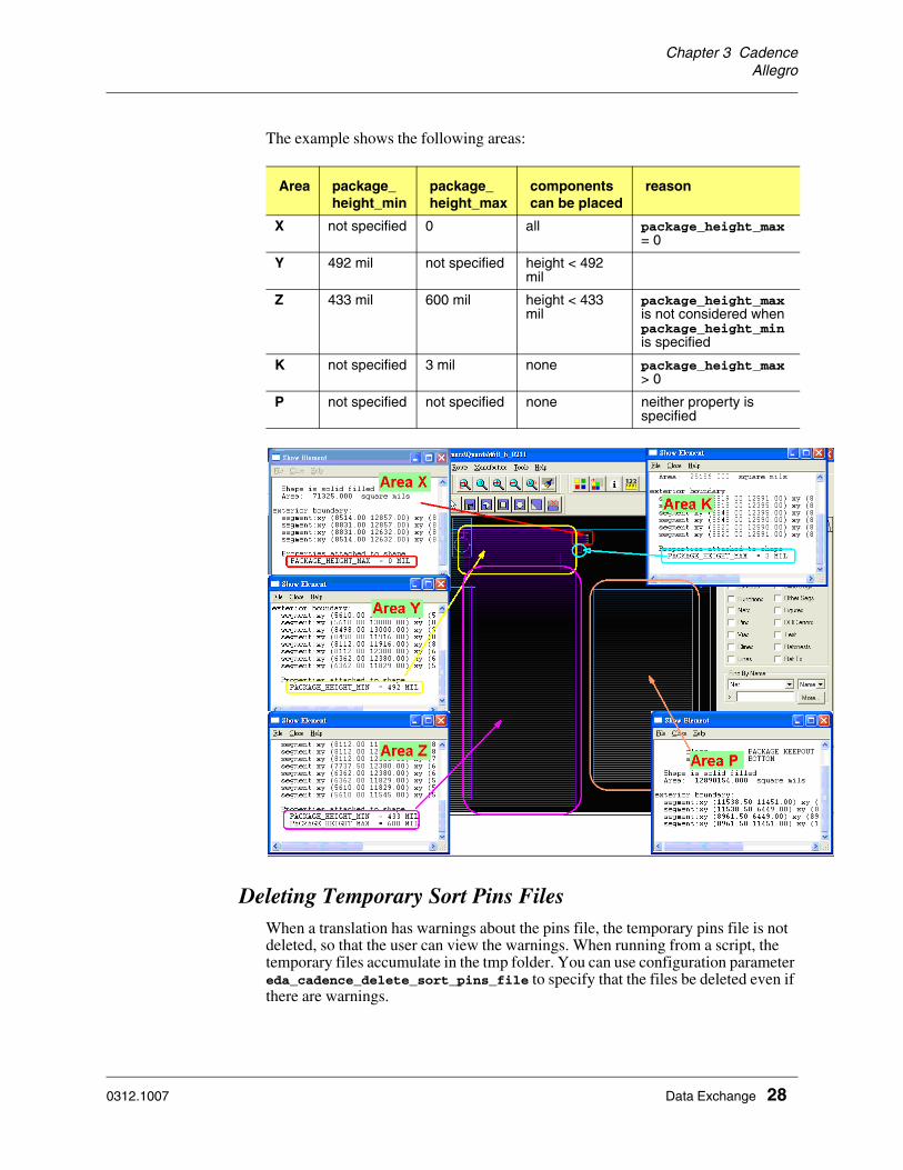
Placing Components Underneath Raised ComponentsIf a component is defined in Allegro as having a value for property package_height_min (the amount of space under the component) or if there are areas of the component with values for package_height_min, this information is stored in ODB++ output and can be used in Trilogy during component analysis.
The height of the component, as defined in the Allegro property package_height_max, is stored in the ODB++ component attribute .comp_height.
A layer (height_top) is created in ODB++ to store height information for areas where there is space underneath components. In this layer, the maximum height of components that can be placed in a particular area is defined in the ODB++ feature attribute .drc_max_height. This attribute is set to the value of package_height_min for components (or areas of components) where package_height_min is specified.
In the example, RefDes J8B1 is a component with three areas defined:
• The main part of the component (area B in the example) is resting on the board, so it has no value for package_height_min.
0312.1007 Data Exchange 26

Chapter 3 CadenceAllegro
• At the two ends of the component (areas A and C in the example), there is a space of height 230 MIL underneath. A component that is placed under an end area of this component is not reported as an error if its height is less than 230 MIL.
Using Height Parameters for Keepout AreasThe parameters package_height_min and package_height_max are interpreted to match their meaning in Cadence Allegro.
package_height_min—the lower limit of the height of the keepout area. If this value is specified for a keepout area, only components with height less than this value can be placed in this area.
package_height_max—package_height_max is not considered when package_height_min is specified. If package_height_min is not specified, this parameter is used to indicate whether all components or no components can be placed in the area, regardless of their height:
• package_height_max = 0 means any components can be placed in this area
• package_height_max > 0 means no components can be placed in this area
To determine the maximum height of components that can be placed in an area, the ODB++ attribute .drc_max_height is set to package_height_min if package_height_min is specified.
0312.1007 Data Exchange 27
Chapter 3 CadenceAllegro
The example shows the following areas:
Deleting Temporary Sort Pins FilesWhen a translation has warnings about the pins file, the temporary pins file is not deleted, so that the user can view the warnings. When running from a script, the temporary files accumulate in the tmp folder. You can use configuration parameter eda_cadence_delete_sort_pins_file to specify that the files be deleted even if there are warnings.
Area package_height_min
package_height_max
componentscan be placed
reason
X not specified 0 all package_height_max = 0
Y 492 mil not specified height < 492 mil
Z 433 mil 600 mil height < 433 mil
package_height_max is not considered when package_height_min is specified
K not specified 3 mil none package_height_max > 0
P not specified not specified none neither property is specified
0312.1007 Data Exchange 28

Chapter 3 CadenceAllegro
Sorting the Pins File Numerically with Numeric Pins LastYou can use option yes_num_last of configuration parameter eda_cadence_sort_pins_numeric to specify that pins be sorted in numerical order, but with numeric pins after pins beginning with a letter.
Note If a configuration file is used by more than one user, and some users have a version of the application from before this option was supported, old versions of the application will interpret the value yes_num_last as no (the default).
Specifying an Alternate Font File To provide an alternate font file so that fonts used in ODB++ match the fonts used in Cadence, place the file in the font directory, and specify the file name in the configuration parameter eda_cadence_font_file_name.
Controlling Handling of Invalid AttributesYou can use configuration parameter attr_value_correct to control how the translator handles illegal attribute values (out of range, etc.) that are input with a design.
Yes - The attribute is reset to its default value, and a message is written to the log.
No - Translation is halted.
Exporting Partial ODB++ DataYou can use the Partial ODB++ option in the ODB++ Inside dialog box to export a subset of the job data.
Note Partial ODB++ data can be exported only from the ODB++ Inside dialog box, and not by using line mode commands.
To export partial ODB++ data:
1. Open the ODB++ Inside dialog box as described in “Creating ODB++ Output” on page 13.
2. Enter the appropriate parameters as described in “Specifying File Options and Output Options” on page 16.
0312.1007 Data Exchange 29

Chapter 3 CadenceAllegro
3. Select Partial ODB++ before running the translation.When this option is selected, the Partial ODB++ Export Setting dialog box opens at the end of the translation.
4. In the box at the top of the dialog box, select one of the following. The table below lists the options that are selected when you select Fab or Assy.
• Fab—layers and data options appropriate for fabrication are selected by default. You can modify the layer selections.
• Assy—layers and data options appropriate for assembly are selected by default. You can modify the layer selections.
• Partial—no layers or data options are selected by default. Use the check boxes on this dialog box to select data for export.
5. In the layer list at the top of the dialog box, select the steps to export. The same layers are exported for all selected steps.
6. Select the layers to export in one of these ways:
0312.1007 Data Exchange 30
Chapter 3 CadenceAllegro
• In the layer list at the top of the dialog box, select the layers to export.
• Select the check boxes for one or more of the layer selection options: Outer copper layers, Silk Screen layers, Solder Paste layers, Solder Mask layers, Drill / Rout layers, Document layers, Inner layers.All layers of the selected types are selected in the layer list. You can clear specific layers or select additional layers in the layer list.Layers are exported according to the layer list, and not according to the layer options that are checked.
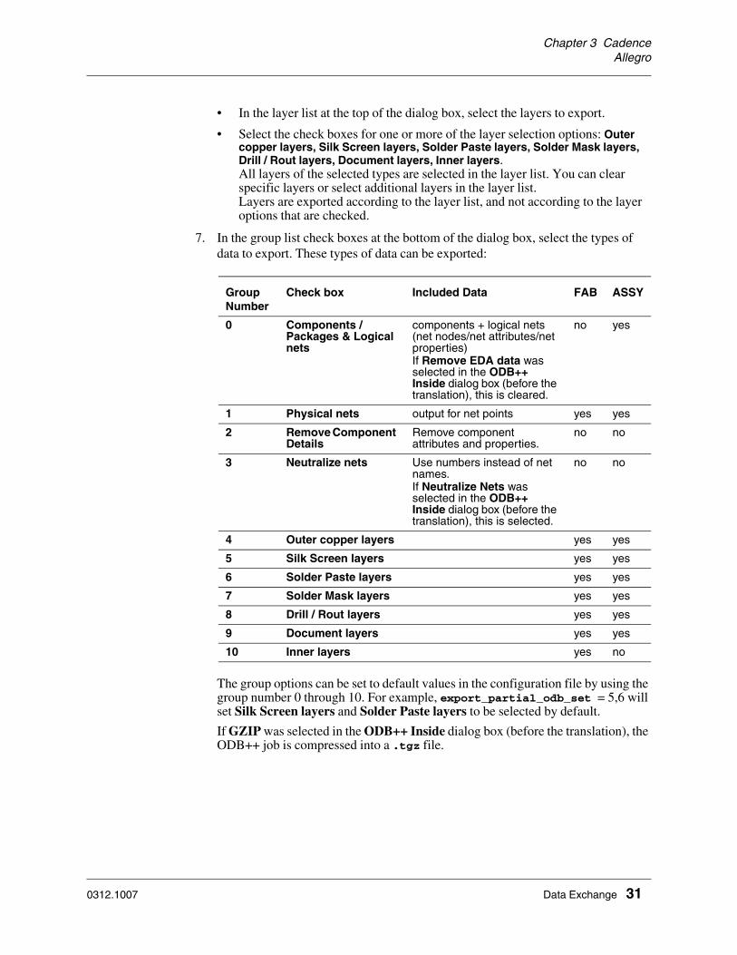
7. In the group list check boxes at the bottom of the dialog box, select the types of data to export. These types of data can be exported:
The group options can be set to default values in the configuration file by using the group number 0 through 10. For example, export_partial_odb_set = 5,6 will set Silk Screen layers and Solder Paste layers to be selected by default.
If GZIP was selected in the ODB++ Inside dialog box (before the translation), the ODB++ job is compressed into a .tgz file.
Group Number
Check box Included Data FAB ASSY
0 Components /Packages & Logical nets
components + logical nets (net nodes/net attributes/net properties)If Remove EDA data was selected in the ODB++ Inside dialog box (before the translation), this is cleared.
no yes
1 Physical nets output for net points yes yes
2 Remove Component Details
Remove component attributes and properties.
no no
3 Neutralize nets Use numbers instead of net names. If Neutralize Nets was selected in the ODB++ Inside dialog box (before the translation), this is selected.
no no
4 Outer copper layers yes yes
5 Silk Screen layers yes yes
6 Solder Paste layers yes yes
7 Solder Mask layers yes yes
8 Drill / Rout layers yes yes
9 Document layers yes yes
10 Inner layers yes no
0312.1007 Data Exchange 31

Chapter 3 CadenceOrcad-Layout
Orcad-LayoutIf you have Valor Enterprise 3000 installed, you can interface directly. The procedure is fully described in Document 0310 Cadence Orcad-Layout Interface manual.
• Orcad-Layout Database
• Creating ODB++ Output
Orcad-Layout DatabaseThe database for the application is a binary file. The Binary file extension is usually.MAX and the ASCII file extension is usually.MIN.
The translator can read either .MIN or .MAX files. Because these files do not contain fabrication data, the generated ODB++ file is not suitable for Fabrication analysis. It only contains the information necessary to support Assembly analysis.
Creating ODB++ OutputTo generate an ODB++ file:
1. Start the Orcad PCB application and load a design.
2. Select File > Export > Layout to ODB++.
0312.1007 Data Exchange 32

Chapter 3 CadenceOrcad-Layout
The Layout to ODB++ window opens.
3. Specify the file names and options:
Input LayoutMAX or MIN
file
The name of the input file. Press <Browse> to navigate.
Output ValorDirectory
The destination directory of the generated ODB++ file. Press <Browse> to navigate.
Output ValorJobname
The name of the ODB++ job.
Overwriteexisting files
Overwrites files with the same name.
Outputcopper pours
Outputs copper pours to the board’s copper layers.
Outputformat
Specifies the type of output to be generated.
Create ODB++ Output - Output is in ODB++
Create XML++ Output - Output is in XML (Extended Markup Language)
4. Click Translate to generate the output file.
0312.1007 Data Exchange 33

Chapter 4 Mentor GraphicsBoard Station
Chapter 4 Mentor Graphics
This chapter discusses the following formats:
• Board Station
• PowerPCB (PADS)
• Expedition
• Supermax ECAD
Board StationIf you have Valor Enterprise 3000 installed, you can interface directly as fully described in Document 0302 Mentor Graphics Board Station Interface manual.
• Board Station Database
• Relevant Files
• Post Processing Options
• Creating ODB++ Output
• Specifying File Options and Output Options
• Specifying Parameters Specific to Mentor Board Station
• Support for Embedded Passive Components
• Controlling Handling of Invalid Attributes
• Controlling the Algorithm Used to Delete Unused Pads
• Assigning Clearance Areas by Drill Center or Area
Board Station DatabaseThe Mentor Graphics Board Station design is a collection of files inside a directory structure. A versioning mechanism exists which maintains a number of copies (typically three) for each file. Most of the files are readable ASCII files, with the notable exception of the file geoms which is one of the most important files.
In the Mentor Graphics Board Station database, the hierarchy of the information is as follows:
• A list of components, where each one refers to a geometry (Package in the Valor notation). A component also has pins which refer to geometries.
• Each geometry is a collection of many features, each being drawn on a logical layer.
0312.1007 Data Exchange 34
Chapter 4 Mentor GraphicsBoard Station
• A special type of geometry, the Artwork Order geometry, contains all the artworks which should be produced and the logical layers to be included inside each. Additional parameters which affect the output may be attached to these artworks.
• The tech file defines the order of the copper layers within the board. This file has no reference to support layers (solder mask, silkscreen, etc.).
• The names of the logical layers carry special meaning in the Mentor Graphics Board Station database.
There are four types of logical layers:
1. Data reporting (such as Errors)
2. Data storage (such as board_outline)
3. Electrical (such as signal, signal_1)
4. Top and bottom mapping (such as pad, pad_1, pad_2)
There are quite complex mapping rules which determine which logical layer, depending on type of layer, will receive a feature. For example, a feature being assigned to layer signal will appear in all layers which are called signal_n where n is an integer number >= 1. A feature in a component geometry which is assigned to layer pad will appear in pad_1 if the component is on the top side and on pad_2 if the component is on the bottom side.
• A special traces file contains all the lines which are used to connect component pins. It also contains the vias which are used in this process and the areas (planes) which were created. Areas can be solid or hatched but also outlines; in which case they are used to define split planes in negative power and ground layers.
• Power and ground layers in the Mentor Graphics Board Station database are always produced negative. Although it is possible to create a signal layer using solid areas which will serve as a ground layer, within Mentor Graphics Board Station it will be considered a signal layer.
• Features which are not a direct part of a component or the connections between them are located inside the board geometry in the geoms file.
• A special panel geometry can be created which adds multiple boards to create a step and repeat pattern. This feature is fully supported by Enterprise 3000 (a panel step containing step and repeat information is created).
Relevant FilesThe following files are required for a correct translation (the listing is in order of importance):
mfg/neutral_file (required)
mfg/geoms_ascii (recommended)
traces (recommended)
tech (recommended)
layers (optional)
0312.1007 Data Exchange 35

Chapter 4 Mentor GraphicsBoard Station
aperture_table (optional)
drill_table (optional)
pins (optional)
variants (optional)
mfg/neutral_file
The neutral_file contains all the required information about components and pin locations. It is not a standard part of the database and has to be created on the Mentor Graphics Board Station system.
Note Components named in the component declaration of this file should not contain spaces. Use ‘A1B2’ and not ‘A1 B2’.
A full neutral_file contains several sections with information:
• BOARD - board attributes
• NET - net points
• GEOM - packages and pins
• COMP - components and toes
• HOLE - drilled holes
• PAD - approximate shape of pads
All of them can be read, except the HOLE section which is not needed since it is derived by other means.
mfg/geoms_ascii
The geoms_ascii file is an ASCII representation of the geoms file inside the pcb directory. It is not a standard part of the database and has to be created on the Mentor Graphics Board Station system.
The geoms_ascii file contains commands written in the Mentor Graphics language called AMPLE. Each command starts with the characters $$ and has the following format:
$$command(param_1, ... , param_n)
The geoms_ascii file is composed of a series of $$create_... commands.
Each $$create command defines one of the following entities:
PANEL
BOARD
COMPONENT
PIN
VIA
DRAWING
GENERIC_PART
STACKUP
All geometries, except the Artwork Order geometry, contain figure commands such as $$circle, $$path, $$text and $$polygon. Some of them include special attributes which are specific for the geometry (such as a drill hole for a pin geometry). The Artwork Order geometry contains the mapping of logical layers to artwork pieces. This geometry must exist at least once in the geoms_ascii file for the translation to succeed.
0312.1007 Data Exchange 36

Chapter 4 Mentor GraphicsBoard Station
tracesfile
The traces file contains the results of the routing process. Legal commands inside the traces file are:
– ST - status line (first and last lines of file)
– XRF - names of layers, referenced later in the file
– UNITS- defines the units used in the file
– WIR,ANT,SEG- describe fully routed connections (lines and vias)
– TIE - synonymous with WIR.
– FIL,ARE/ARS,ISL/ISS, VER- definition of area-fill/power-fill shapes and cutouts.
– TTI,TTT - apply actual signal thermals to the design,according to the TTI (Thermal Tie Instance)statements that relate to the TTT (Thermal TieTemplate) statements.
– TET- teardrop templates.
Note The version of the Mentor Graphics input is automatically detected from the traces file.
techfile
The tech file contains the physical order of copper layers within the board. It also contains information about geometries which do not go through the board (blind and buried vias). Another valuable piece of information inside the tech file is the net rules which are needed when generating signal layer thermal pads and mixed layers.
The tech file is also composed of AMPLE commands. Here is an example of a section which defines the physical layer order:
$$define_physical_layer( 1, “comp_ver”, “SIGNAL_1”, “PAD_1”);
$$define_physical_layer( 2, “int1_hor”, “SIGNAL_2”);
$$define_physical_layer( 3, “int2_ver”, “SIGNAL_3”);
$$define_physical_layer( 4, “int3_hor”, “SIGNAL_4”);
$$define_physical_layer( 5, “vcc”, “POWER_1”);
$$define_physical_layer( 6, “scsivcc”, “POWER_2”);
$$define_physical_layer( 7, “665vcc”, “POWER_3”);
$$define_physical_layer( 8, “752vcc”, “POWER_4”);
$$define_physical_layer( 9, “avcc”, “POWER_5”);
$$define_physical_layer( 10, “cpu3v”, “POWER_6”);
$$define_physical_layer( 11, “ctlvcc”, “POWER_7”);
$$define_physical_layer( 12, “cvcc”, “POWER_8”);
$$define_physical_layer( 13, “hvcc”, “POWER_9”);
$$define_physical_layer( 14, “iovcc”, “POWER_10”);
$$define_physical_layer( 15, “mvcc”, “POWER_11”);
$$define_physical_layer( 16, “gnd”, “POWER_12”);
$$define_physical_layer( 17, “752gnd”, “POWER_13”);
$$define_physical_layer( 18, “int4_ver”, “SIGNAL_5”);
$$define_physical_layer( 19, “int5_hor”, “SIGNAL_6”);
$$define_physical_layer( 20, “int6_ver”, “SIGNAL_7”);
$$define_physical_layer( 21, “cond_hor”, “SIGNAL_8”, “PAD_2”);
0312.1007 Data Exchange 37
Chapter 4 Mentor GraphicsBoard Station
In the example above, there are only 8 physical layers. The command name $$define_physical_layer is misleading since these are actually logical layers. This section, combined with the stackup definition, provides the information necessary for creating the physical board structure.
layersfile
The layers file contains layer data that describes the arrangement and characteristics of the system data layers. The Mentor Graphics Board Station classifies layers into four groups. In particular, top and bottom layers are treated differently than other layers. The layers file may add more names which will be treated as top and bottom layers.
The layers file is an ASCII file, and is not written in AMPLE.
aperture_table
file
The aperture_table file contains information about Dcodes (the wheel). Some pieces of information can only be derived by looking in this file. These include:
• The spot pad that will be used for NPTH drill holes (taken by default as the minimal circular flash aperture)
• The brush that is used for area fills
• The size of tiebars for signal layer thermals
• The definition of thermals used in P&G layers
drill_ tablefile
The drill_table file includes the mapping of drill bits to the positions in a drill magazine. For each drill position, the drill table defines a drill size, hole tolerances, hole plating and the name of generic geometry used for creation of the drill symbol for a specific drill size. These names are used during translation to create drill symbols on the relevant documentation layers.
pins file The pins file contains pin properties (name, value). The following is a pins file, an ASCII file, for the property PINREF.
# BOARD STATION PINS FILE FORMAT 2.0
# Pin property is presented in format (prop_name, prop_value).
#
# PIN Reference-Pin_no Properties
PIN C1-1 PINREF,"IN,0.0,0.12,0,CC,0.06,0.06,0.01,std,1,U,+")
variants file The variants file contains a list of variants and their description. The following is a variant file; it is an ASCII file:
# PCB_DA VARIANTS FILE FORMAT 1.1
# Date : Tue Mar 19 20:02:03 2002
#
#########################
# Variant Definitions #
#########################
VARIANT OT_AD
DESCRIPTION "201130185"
0312.1007 Data Exchange 38

Chapter 4 Mentor GraphicsBoard Station
VARIANT OT_T
DESCRIPTION "201130186"
VARIANT OTMUX
DESCRIPTION "201130184"
Artwork vs.Layers Order
The ‘physical’ layers order is defined in the Mentor Graphics Board Station database in the tech.tech_XXX file by the following command:
$$define_physical_layer( NN,...)
Where NN defines the physical layer sequence in the stackup.
However, some of Mentor Graphics' ‘physical’ layers are really logical ones, that is, several logical layers are mapped to one physical layer in the stackup.
The <list of logical layers> in the geoms_ascii file command defines logical layers that are mapped to a single artwork:
$$attribute( "ARTWORK_##_LAYER_DEFINITION","<list of logical layers>");
(the ## is irrelevant to the artwork sequence in the stackup)
This command defines the physical layer (artwork) that contains data from all logical layers named in this <list>.
For example, you may notice that the SIGNAL_1 layer is usually defined in ARTWORK_01_LAYER_DEFINITION. However, solder paste, solder mask and silk screen layers must be ‘upper’ in the stackup. Therefore, SIGNAL_1 layer will not be mapped to the first artwork in the stackup.
The definitions in the tech file are used for copper layers. The regular order is used, as always, for the other board layers.
Post Processing OptionsThese actions can be performed on the fly, during output:
• Adding teardrops
• Eliminating non-functional pads
• Offsetting the design in X, Y or both
• Creating signal layer thermals
0312.1007 Data Exchange 39

Chapter 4 Mentor GraphicsBoard Station
In addition, you can choose whether you want to output only the board (one-up) or a multi-board panel (with Step & Repeat).
Creating ODB++ OutputCompletion of the Mentor Graphics Board Station artwork table is a prerequisite for creation of ODB++ from the Mentor Graphics Board Station database. The artwork order table is used to create the physical layer stackup of the board, and the mapping of Mentor Graphics logical design layers to physical board layer graphics.
To generate an ODB++ file:
1. Open the Mentor BoardStation ODB++ Export dialog box in one of these ways:
• Start the Design Manager and select a design. Start FabLink. Select File > Export > To ODB++.
0312.1007 Data Exchange 40

Chapter 4 Mentor GraphicsBoard Station
If you do not have the ODB++ translator installed, the option is not available. The translator is available as a downloadable service pack to Mentor Graphics Board Station Customers, with a current Mentor Graphics support contract.
• In Windows, select Start > Programs > Valor > MBS2ODB translator > MBS2ODB or enter this command line: %MBS2ODB_DIR%\mbs2odb
• In UNIX, enter this command: $MBS2ODB_DIR/mbs2odb.
The Mentor BoardStation ODB++ Export dialog box opens.
If the Valor Universal Viewer is not installed at your site, the VUV icon is not displayed. Contact Valor for information about the VUV.
2. Specify basic options as described in “Specifying File Options and Output Options” on page 42.
3. If you will be outputting to an ODB++(X) file, select ODB++(X) and click Show ODB++(X) Settings to open the XML Export Setting dialog box and define ODB++(X) parameters. See “Defining ODB++(X) Settings” on page 9.
4. Click the Show Options icon to expand the ODB++ Inside dialog box to display tool-specific parameters. See “Specifying Parameters Specific to Mentor Board Station” on page 43.
5. To open the translator’s manual in PDF format, click the Help icon.
The configuration parameter gns_pdf_viewing_prog is set with the path and command to run a PDF viewer. For example: gns_pdf_viewing_prog=/sw/bin/acroread -useFrontEndProgram where /sw/bin/acroread is where the PDF viewer is stored.
6. To quit the translation program, click the Quit icon.
0312.1007 Data Exchange 41
Chapter 4 Mentor GraphicsBoard Station
7. Click the Translate icon to translate the job. The Selected Options Viewer opens to shows the parameters that will be used in the translation.
• To close the Selected Options Viewer and return to the ODB++ Inside dialog box, click Back.
• Click Accept in the Selected Options Viewer to start the translation process.
8. To view the translator log, click the View Log icon. All program messages are written to the log.
To clear the log file, click Clear Log.
After translation, click the VUV icon to display the design in the Valor Universal Viewer (VUV). If the Valor Universal Viewer is not installed at your site, the VUV icon is not displayed. Contact Valor for information about the VUV.
Specifying File Options and Output OptionsSpecify these parameters in the Mentor BoardStation ODB++ Export dialog box:
Input Path Enter the location directory of the input file.
Output Path Enter the destination directory of the generated ODB++ file. The output file is put in the manufacturing (mfg) directory within the design directory structure.
Output JobName
Enter the name of the ODB++ file.
Log File Path Specifies the path to the log file. Press <Browse> to navigate. By default a new log file is created for each translation. If the ‘Append’ checkbox is marked, log messages will be appended to the most recent log file.
Remove EDAdata
Removes Component/Package information from the ODB++ job.
0312.1007 Data Exchange 42

Chapter 4 Mentor GraphicsBoard Station
NeutralizeNets
Renames nets numerically.
GZIP Specifies whether to compress the ODB++ job. The ODB++ job is made up of several files describing the output. If activated, compression creates a single ‘tar’ed and zipped file. The default is not to compress.
ODB++(X) ODB++(X) is a representation of the ODB++ format in XML. Select ODB++(X) to export in this format.
PartialODB++
Export partial ODB++ output.
Export asODBV6
By default, information is exported in ODB++ Version 7 format. Select this option to export to the earlier ODB++ format.
ShowODB++(X)
Settings
The ODB++(X) interface lets you decide what data the ODB++(X) file will contain. Click Show ODB++(X) Settings to view/modify the export options. See “Defining ODB++(X) Settings” on page 9.
Specifying Parameters Specific to Mentor Board StationClick the Show Options icon on the Mentor BoardStation ODB++ Export dialog box to display tool-specific parameters.
0312.1007 Data Exchange 43

Chapter 4 Mentor GraphicsBoard Station
If the Valor Universal Viewer is not installed at your site, the VUV icon is not displayed. Contact Valor for information about the VUV.
AdditionalParameters
Read DRC features - Enables reading in of DRC data (Such as: routing outline, placement_outline, via_keepout) into the translated job. The default is No.
Round corners - Creates round corner surfaces, according to fill brush, or according to the traces file description. The default is No.
Read $NONE$ net info - Enables users to read in $NONE$ nets defined in the neutral_file, for netlist analysis purposes. The default is Yes.
Process breakout geometries - Ignores component breakout geometries, as required for jobs routed by external tools. When Read Traces is set to Yes, Process breakout geometries must be set to No to prevent shorts. You cannot set both Read traces and Process breakout geometries to Yes to disallow unintended shorts. The default is No.
Read in Unplated - Builds padstacks for unplated holes. The default is Yes.
Ignore Comp. Layout Type - Ignores the Component_Layout_Type property of a Mentor Graphics Board Station component, that affects the .comp_mount_type attribute of a ODB++ component. The default is No.
Component Geom Outline - Overwrites the component outline with the data in COMPONENT OUTLINE layers in geoms_ascii, if it exists. If this option is not selected, the component outline is read from the neutral_file. (default)
Fill Hatch Mode - Specifies how hatched surfaces are to be filled. The default is Default.
• None - all hatch cells are empty (not filled).
• Part - only hatch cells around the border are filled.
• All - all hatch cells are filled solid (convert hatch to solid).
• Default - fill hatch surface according to Mentor Graphics database design version: prior to version 8.6.5 it is the same as None, afterwards it is the same as Part.
Fill Hatch around Traces -
• All - fills the hatch sections touched by a trace.
• Match Hatch - fills only the traces matching the hatch pattern.
• No - does not fill any of the hatch.
Fill Hatch around Pads - to fill the hatch touched by pads.
Pins NFPRemoval
Enables padstack optimization of unused pins and pins with no net.
None - no removal of non-functional pads
Unused Pins - removes isolated pads (not connected to any other copper pad, trace, or surface)
Pins with No Net - removes pads in net $NONE
The following rules are applied:
0312.1007 Data Exchange 44

Chapter 4 Mentor GraphicsBoard Station
• Pads are removed on signal layers only.
• Pads are not removed for external signal layers of the padstack span. (Does not apply to pins with the No Net option.)
• SMD pins are not processed.
• Only isolated pads (not connected to any other copper pad, trace or surface) are removed. (Does not apply to pins with the No Net option.)
• Each modified padstack is assigned with the attribute .pf_optimized on the pad in the matching drill layer. This enables the identification of layers where padstack optimization, the removal of pads, has taken place.
Vias NFPRemoval
Enables padstack optimization of unused vias.
None - no removal of non-functional pads
Unused Vias - removes isolated pads (not connected to any other copper pad, trace, or surface)
Rules are the same as described in Pins NFP Removal.
Read tracesflag
Specifies which trace routing records are to be read from the traces file.
Options are: Yes, No, All. The default is Yes.
Yes - reads complete wired traces (WIR records)
No - does not read any traces
All - reads complete and incomplete wired traces (WIR and INC records) from traces file.
Componentoutline by
Enables choice of Place or Body geometry to determine component outline. Each component outline must be a single, closed polygon. Options are: Place, Body. The default is Place.
Place - from the Placement records
Body - from the Body records
Placement Override - sets placement outline for both top and bottom sides according to that defined for the top side.
Thermalpads rotation
by
Specifies whether ties are to be rotated.
Options are: Component, None. The default is Component.
Component - instructs the system to rotate the ties together with the component
None - does not rotates the ties. Use this option when you want to rotate the ties manually.
Read inPanel/Boardgeometries
Determines whether to read in Board, Panel or Flatten Panel geometry.
Board - reads in board data only.
Panel - Board and all panels are read in. Panels are translated into ODB++ Step & Repeat data.
0312.1007 Data Exchange 45
Chapter 4 Mentor GraphicsBoard Station
Flatten Panel - panel data is replicated (components and features), as if the step contains only one board.
Minimum linewidth
Specifies the number of mils to extend the outline on negative planes. The value is between 0 to 2.5. The default is 0 mils.
Symboltolerance
Any new symbol that is encountered during the translation is compared with symbols that have previously been generated during the translation. If the new shape is within the tolerance value specified, the previous shape is used. The value is between 0 to 0.5. The default is 0.2 mils.
Dummy PadName
Name of dummy pads (zero diameter drills/pads, sometimes required by Mentor Graphics) added to netlist after translation.
Model file Use thermal model file - enables setting of the Thermal file and model to be used.
If known, type the name of the file and the path in the text boxes or press to locate the thermal file. If you do not specify a thermal model file, a default model is used that uses direct connect and no thermals. For an explanation of the thermal model, see Appendix A.
Support for Embedded Passive ComponentsEmbedded passive components in Mentor Board Station designs can be stored as such in ODB++.
To import embedded passive component information:
1 Set configuration parameter eda_mentor_translate_emb_components:
– Yes - components on inner layers are assigned attribute .is_burried, and embedded passive layers are created, on which embedded components are added as features. Because components are marked as belonging to a specific copper layer, The embedded passives layer in ODB++ is related to this copper layer. In the job matrix it appears above its copper layer.
– No - embedded components are added to the component layer.
2 Import the job.
Feature attribute .ecmp_name is assigned to the embedded passive features, with the component name (RefDes) as its value. The embedded passive value (resistance or capacity) is not read.
3 Set the embedded component feature attributes as necessary. You can change .ecmp_name and/or define .ecmp_value, .ecmp_min_value and .ecmp_max_value.
Controlling Handling of Invalid AttributesYou can use configuration parameter attr_value_correct to control how the translator handles illegal attribute values (out of range, etc.) that are input with a design.
0312.1007 Data Exchange 46

Chapter 4 Mentor GraphicsBoard Station
Yes - The attribute is reset to its default value, and a message is written to the log.
No - Translation is halted.
0312.1007 Data Exchange 47
Chapter 4 Mentor GraphicsBoard Station
Controlling the Algorithm Used to Delete Unused Pads
Configuration parameter eda_mentor_rmv_fully_isolated can be used to control the algorithm that determines whether pads are removed when Pins NFP Removal = Unused Pins and Vias NFP Removal = Unused Vias.
Yes (default) - Only fully isolated pads are removed.
No - The following pads are considered to be unconnected and non-functional:
• a single totally isolated pad
• two pads touching or intersecting
• a pad transversed by a trace not through its center
• a pad touching a surface where its center is not inside the surface
Assigning Clearance Areas by Drill Center or Area
In a job with a split plane, pads are assigned to a clearance area according to the center of the drill or the whole area of the drill, depending on the value of the new configuration parameter eda_mentor_use_drill_size.
Yes - Use the whole area of the drill.
No - Use the center of the drill. (default)
0312.1007 Data Exchange 48

Chapter 4 Mentor GraphicsPowerPCB (PADS)
PowerPCB (PADS)If you have Valor Enterprise 3000 installed, you can interface directly. The procedure is fully described in Document 0304 Mentor Graphics PowerPCB Interface manual.
It is not possible to generate ODB++ output directly from the Mentor Graphics PowerPCB application. An ASCII file must be created from the PowerPCB job and sent to manufacturers that use Trilogy 5000. This file has the suffix .asc and contains all data necessary for translation.
The following steps should be used to generate the ASCII file:
• Defining CAM Documents
• Filling Copper Pour Outlines - Set Pour Manager to ‘Flood All’. If there are overlapping copper pour outlines, find them and manually fill them one by one. If the design uses split/mixed planes, the planes should be filled in as well.
• Saving Split/Mixed Plane Data
• Creating the ASCII File
Defining CAM DocumentsThe layers created by the translation process do not correspond to the layers defined in the PowerPCB job. Rather, they correspond to the CAM documents defined for the job since they must represent the physical layer stackup of the board.
Only three layers are created for a PowerPCB job with no defined CAM documents: the top and bottom component layers, and the drill layer. All other layers, electrical and non-electrical, correspond to CAM documents defined in the job.
Note Layer names should not begin with a period, because this translates into a hidden entity file.
CAM documents are defined using the Define CAM Documents interface.
• Start PowerPCB.
• Select File > CAM. The Define CAM Documents window opens:
0312.1007 Data Exchange 49

Chapter 4 Mentor GraphicsPowerPCB (PADS)
The following table lists the possible CAM document types and their corresponding layer types:
By default, many designers use layer 20 to draw the component outline. The translator searches this layer for drawings to determine the component outline. If no shapes are found on this layer, a fallback algorithm is used.
Filling Copper Pour OutlinesWhen translating a PowerPCB job, unhatched copper areas require processing, as they do when generating CAM output. Copper pours that have not been flooded are exported to the PowerPCB-ASCII file as an area outline without the various required clearances that the Flood process creates to avoid shorting different nets.
Once a copper pour area is flood filled, it does not have to be reflooded. When reloading a saved job with flooded copper pour areas the areas will not display as filled in the PowerPCB window. However, they will contain all data necessary for translation, which means clearances are defined in the data.
Therefore, before creating the PowerPCB-ASCII file, all copper pours must have been flooded at least once.
CAM Document Type Trilogy 5000 Layer
Routing Signal Layer
Plane P/G Layer
Silkscreen Silk Screen Layer
Paste_Mask Solder Paste Layer
Solder_Mask Solder Mask Layer
Custom Documentation Layer
Assembly Documentation Layer
Drill_Drawing Documentation Layer
NC_Drill Not applicable
Verify_Photo Not applicable
0312.1007 Data Exchange 50

Chapter 4 Mentor GraphicsPowerPCB (PADS)
To fill copper pour outlines:
• Select Tools > Pour Manager from the PowerPCB menu:
• In the Pour Manager dialog box, select the Flood tab. Check Flood All and click Start:
This action does not always fill all copper pours. Occasionally, if there are overlapping copper pour outlines, they will be left untouched. You must find these areas and manually fill them one by one. To do this, press <Shift+Click> on a copper pour outline, then right-click and select Flood.
After filling all copper pour areas, you can export and translate the job.
0312.1007 Data Exchange 51

Chapter 4 Mentor GraphicsPowerPCB (PADS)
Saving Split/Mixed Plane DataIf your design uses split/mixed planes, they should be processed in a similar fashion to copper pours: that is, they must be filled in and then exported.
To save split/mixed plane data:
• Select Tools > Pour Manager from the PowerPCB menu.
• In the Pour Manager dialog box, select the Plane Connect tab, and click Select All to process all split/mixed plane layers:
• Click Start to fill in the split/mixed plane layers.
• Click Setup. The Preferences dialog box opens:
• Under Save to PCB File, select All Plane Data.
• Click OK.
• Close the Pour Manager dialog box.
0312.1007 Data Exchange 52
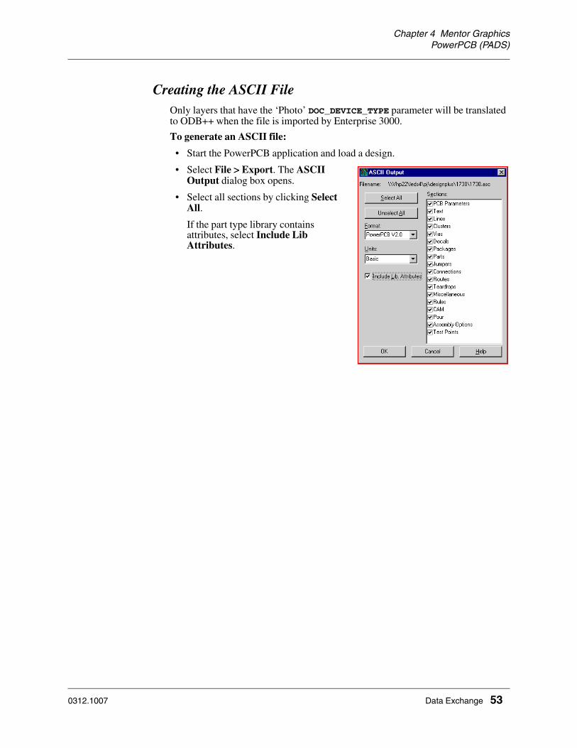
Chapter 4 Mentor GraphicsPowerPCB (PADS)
Creating the ASCII FileOnly layers that have the ‘Photo’ DOC_DEVICE_TYPE parameter will be translated to ODB++ when the file is imported by Enterprise 3000.
To generate an ASCII file:
• Start the PowerPCB application and load a design.
• Select File > Export. The ASCII Output dialog box opens.
• Select all sections by clicking Select All.
If the part type library contains attributes, select Include Lib Attributes.
0312.1007 Data Exchange 53
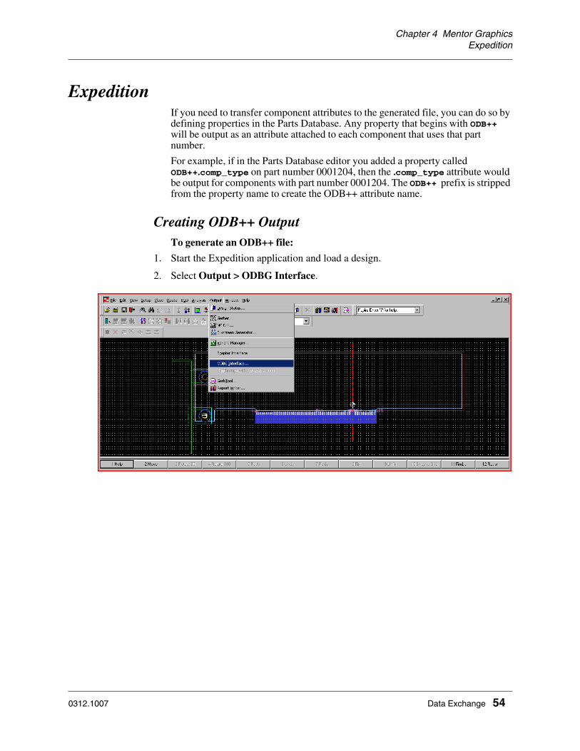
Chapter 4 Mentor GraphicsExpedition
ExpeditionIf you need to transfer component attributes to the generated file, you can do so by defining properties in the Parts Database. Any property that begins with ODB++ will be output as an attribute attached to each component that uses that part number.
For example, if in the Parts Database editor you added a property called ODB++.comp_type on part number 0001204, then the .comp_type attribute would be output for components with part number 0001204. The ODB++ prefix is stripped from the property name to create the ODB++ attribute name.
Creating ODB++ OutputTo generate an ODB++ file:
1. Start the Expedition application and load a design.
2. Select Output > ODBG Interface.
0312.1007 Data Exchange 54

Chapter 4 Mentor GraphicsExpedition
The ODBG Interface dialog box opens.
3. To open the Help Browser window for an explanation of the parameters of the translator, click the Help button.
4. Select the appropriate Output options:
Part numbers Checks if Part numbers are written out to the ODB++ file as stroked text.
Assemblylayers
Determines if top and bottom layers will be written to the ODB++ file. If used the layer is written out as documentation layers.
GeneratedSilkscreen
data
Select only when silkscreen data is generated by using the Silkscreen Generator. Otherwise, the regular silkscreen data will be used.
Drill drawinglayer
Determines if data on the drill drawing layer is output to the ODB++ file. If used, the layer will be created as a documentation layer.
5. To have the mapping grid available to map user defined layers, select User layers.
6. Select Launch ODB++ Convertor. This option must be selected for ODB++ creation.
7. Click OK to start the generation of ODB++.
0312.1007 Data Exchange 55

Chapter 4 Mentor GraphicsSupermax ECAD
Supermax ECADSupermax ECAD offers solutions for embedded component technology, MCM, hybrid, RF and advanced packaging design. Supermax offers the option of outputting ODB++ format.
ODB++ output can be created from the CAM output dialog box or from the File > Export > ODB++ option.
• Creating ODB++ Output from the CAM Output Dialog Box
• Creating ODB++ Output from the File > Export Option
• Output - Mapfile
Creating ODB++ Output from the CAM Output Dialog BoxTo generate an ODB++ file from the CAM output dialog box:
• Start the Supermax application and load a design.
• In the CAM output dialog box, specify ODB++ as an output operation.
• Click Generate to start the generation of ODB++ output.
Creating ODB++ Output from the File > Export OptionTo generate an ODB++ file from the File > Export option:
• Start the Supermax application and load a design.
• Select File > Export > ODB++. The Export ODB++ dialog box opens
• Click Browse to specify a destination directory for the ODB++ file.
• Click Browse to specify the location of the mapping file.
0312.1007 Data Exchange 56

Chapter 4 Mentor GraphicsSupermax ECAD
• To exit the ODB++ generation dialog, click Cancel.
• To display the application help information, click Help.
• Click OK to start the generation of ODB++ output. When the ODB++ file has been successfully generated, a message is displayed.
Output - MapfileThe mapfile contains a layer mapping section and an attribute section for net and component properties. The mapping file follows the Supermax ECAD mapping file standard. The default map file is found in the $IPHOME/tables/odbmap directory.
LayerMapping
section
The layer mapping section of the mapping file contains an ODB++ layer name and a Supermax ECAD layer name. The ODB++ context, type and side are optional:
If you will be performing layer merge, the layers should be added to the layer section in the mapping file. For example, on layer signal1, if you want to add the layer called TopCoupon, then the layer TopCoupon should be added in the layer section as: signal1 TopCoupon.
Recommended ODB++ layer names, context, type and side:
where,
NN is electrical layer number seen from the top side of the design.
MM is drill layer number.
ODB++ [Layer]
SM ECAD Layer
ODB_context ODB_type ODB_side
ts TopSilk silkscreen document top
tref TopRefDes silkscreen document top
bs BotSilk silkscreen document bottom
bref BotRefDes silkscreen document bottom
Layer Type ODB LayerName
Context Type Side
Signal sigNN Board Signal top/bottom
Plane sigNN Board Plane top/bottom
Inner sigNN Board Signal inner
Top solder paste spt Board Solder paste top
Bottom solder paste bts Board Solder paste bottom
Top solder mask smt Board Solder mask top
Bottom solder mask smb Board Solder mask bottom
Drill layers drlMM Board Drill none
0312.1007 Data Exchange 57

Chapter 4 Mentor GraphicsSupermax ECAD
Possible ODB layer context values are: board, misc
Possible ODB layer types are: signal, plane, inner, mixed, solder_mask, solder_paste, silkscreen, drill, rout, document, components.
Possible ODB layer sides are: top, bottom, inner, none.
AttributeMapping
section
The component attribute contains the ODB++ component property name and the Supermax ECAD component property name.
[Attribute]
The net attribute contains the ODB++ net property name and the Supermax ECAD net property name.
[Attribute]
For example, the net clock has a user property called Critical and carries the value of true. The ECAD_net_property_name should be changed to Critical and the ODB_net_property_name changed to .critical_net (i.e. the name to be exported). If there is no entry in the Mapfile matching the property, it is not output.
type comp
Name ODB_comp_property_name ECAD_component_property_name
type comp
Name ODB_net_property_name ECAD_net_property_name
0312.1007 Data Exchange 58
Chapter 5 ZukenVisula
Chapter 5 Zuken
This chapter discusses the following formats:
• Visula
• Board Designer (CR5000)
• PWS (CR3000)
• Cadstar
VisulaIf you have Valor Enterprise 3000 installed, you can import Visula files as described in document 0305 Zuken CADIF Interface manual.
Input required for translation is an evaluated CADIF file that is generated by the ODB++ output program. An evaluated cadif.file, contains all data necessary to create a job. It is generated from an ASCII file with the suffix .paf by activating an ifd script in the Visula Layout Editor.
An evaluated cadif.file always contains the following line:
(dataSetARCHIVE ROUTE_RULES PLACE_RULES PIN_SIGNALS PAD_EVAL ROUTE_ISO)
A non-evaluated cadif.file does not contain this line. Non-evaluated CADIF files (partial CADIF files) will be translated. However, the ODB++ data created cannot be used for full fabrication analysis.
• Creating ODB++ Output from the Visula Interface Menu
• Creating ODB++ or ODB++(X) using a Standalone Program
• Specifying File Options and Output Options
• Specifying Parameters Specific to Zuken Visula
Creating ODB++ Output from the Visula Interface MenuThe ODB++ translator is supplied by Zuken and can be downloaded from the Zuken web pages.
When using the Visula Interfaces menu, the dialogs and default responses are determined by an ifd file that typically resides in $red_programs/cad_iface. You can create your own ifd files and store them locally. When the Visula interface menu is accessed within the Layout application, the application will search for ifd files in the following sequence:
• $red_programs/cad_iface
• $red_data/cad_iface
0312.1007 Data Exchange 59

Chapter 5 ZukenVisula
• $HOME/red_data/cad_iface
To change the default responses for ODB++ output, the valorodb.ifd file that is supplied with the translator should be edited and copied to one of these locations.
A full description of the ifd mechanism may be found in the Visula on-line documentation manual - CAD/CAM Interfaces.
To generate an ODB++ file from the Visula Interface menu:
1. Start the Visula application and load a design.
2. Select Job > Input/Output > Interfaces > Valor ODB++ Output. The Valor ODB++ Output dialog box opens.
3. Specify the output path and file.
4. Click OK to perform translation.
Creating ODB++ or ODB++(X) using a Standalone Program1. Open the Zuken Cadif to ODB++ translator dialog box in one of these ways:
• In Windows, select Start > Programs > Valor > cadif to odb++ translator > Cadif2ODB or enter this command line: VISULA_CADIF2ODB%\cadif2odb.
• In UNIX, enter this command: $VISULA_CADIF2ODB/cadif2odb.
Output path The directory in which the generated ODB++ files will be placed.
Output file The ODB++ filename.
0312.1007 Data Exchange 60

Chapter 5 ZukenVisula
The CADIF to ODB++ window opens.
If the Valor Universal Viewer is not installed at your site, the VUV icon is not displayed. Contact Valor for information about the VUV.
2. Specify basic options as described in “Specifying File Options and Output Options” on page 62.
3. If you will be outputting to an ODB++(X) file, select ODB++(X) and click Show ODB++(X) Settings to open the XML Export Setting dialog box and define ODB++(X) parameters. See “Defining ODB++(X) Settings” on page 9.
4. Click the Show Options icon to expand the Zuken Cadif to ODB++ translator dialog box to display tool-specific parameters. See “Specifying Parameters Specific to Zuken Visula” on page 63.
5. To open the translator’s manual in PDF format, click the Help icon.
The configuration parameter gns_pdf_viewing_prog is set with the path and command to run a PDF viewer. For example: gns_pdf_viewing_prog=/sw/bin/acroread -useFrontEndProgram where /sw/bin/acroread is where the PDF viewer is stored.
6. To quit the translation program, click the Quit icon.
0312.1007 Data Exchange 61

Chapter 5 ZukenVisula
7. Click the Translate icon to translate the job. The Selected Options Viewer opens to shows the parameters that will be used in the translation.
• To close the Selected Options Viewer and return to the Zuken Cadif to ODB++ translator dialog box, click Back.
• Click Accept in the Selected Options Viewer to start the translation process.
8. To view the translator log, click the View Log icon. All program messages are written to the log. To clear the log file, click Clear Log.
After translation, click the VUV icon to display the design in the Valor Universal Viewer (VUV). If the Valor Universal Viewer is not installed at your site, the VUV icon is not displayed. Contact Valor for information about the VUV.
Specifying File Options and Output OptionsSpecify these parameters in the Zuken Cadif to ODB++ translator dialog box.
Input Path Enter the location directory of the input file. The default directory is the path to the current working directory.
Output Path Enter the destination directory of the generated ODB++ file. The default directory is the path to the current working directory.
Output Job Name
The name of the ODB++ file.
Log File Path The path to the log file.
Append By default a new log file is created for each translation. If Append is selected, log messages are appended to the most recent log file.
Remove EDA data
Component/Package information is not written to the ODB++ job.
Neutralize Nets Nets are renamed numerically.
0312.1007 Data Exchange 62

Chapter 5 ZukenVisula
Specifying Parameters Specific to Zuken VisulaClick the Show Options icon on the Zuken Cadif to ODB++ translator dialog box to display tool-specific parameters.
If the Valor Universal Viewer is not installed at your site, the VUV icon is not displayed. Contact Valor for information about the VUV.
Cadif SourceFile
Specify the source location of the CADIF file.
• PCB - searches in the pcb sub-directory.
• MCM - searches in the mcm sub-directory.
GZIP Specifies whether to compress the ODB++ job. The ODB++ job is made up of several files describing the output. If activated, compression creates a single tar’ed and zipped file. The default is not to compress.
Partial ODB++ Exports a subset of the information. See “Exporting Partial ODB++ Data” on page 65.
ODB++(X) ODB++(X) is a representation of the ODB++ format in XML. Select ODB++(X) to export in this format.
Export as ODBV6
By default, information is exported in ODB Version 7 format. Select this option to export to the earlier ODB format.
Show ODB++(X) Settings
The ODB++(X) interface lets you decide what data the ODB++(X) file will contain. Click Show ODB++(X) Settings to view/modify the export options. See “Defining ODB++(X) Settings” on page 9.
0312.1007 Data Exchange 63

Chapter 5 ZukenVisula
ExcludeLayers
Layers to be excluded from translation. Separate layer names with a semi-colon ‘;’.
Solder PasteLayers
Layers to be translated as solder-paste layers. A number of layers can be specified together either by name or logical ID, individually or by range, separated by semi-colon (;).
TopSilkscreen
Layers
Layers to be translated as top silkscreen layers. A list of layer names can be specified together either by logical IDs or ranges of either, separated by semi-colon (;).
ClearanceGap
The Clearance expansion (gap) to be used on P&G layers when the input file is not in full mode.
Use matrixfile
You can provide a matrix file to provide a connection between CADIF britup files and ODB++ layers. The matrix file can make either of these types of connection:
• Selected features in several CADIF layers to a specific ODB++ layer (follows Visula WYSIWYG approach).
• A single CADIF layer to its ODB++ counterpart.
An example of a Matrix file:
**************************************************************#ODB++ Zuken Cadif Interface Matrix definition#Format - must be “1.0”FORMAT 1.0#directory#DIR <path>#location of britup files - can be skippedDIR /zj/britup_test/7#layers#LAYER CADIF <layer_name>#put the layer name from the cadif file
#LAYER BRITUP <file_name> <type> <side>#File name can be absolute or relative to DIR#Type can be one of the following: sig, pg, mix, ss, sm, sp, doc#Long names for types are also allowable: signal, power_ground, mixed,#silk_screen, solder_mask, solder_paste, document#Leave name as “doc”, system will auto-detect (recommended)#Side can be top, bottom or auto; empty field means “auto”. System checks#layer side and type against internal definition and may change it accordingly.
LAYER BRITUP tal topLAYER BRITUP paste-top.bri sp topLAYER BRITUP resist-top.bri sm topLAYER CADIF L5LAYER CADIF F6LAYER BRITUP paste-bottom.bri sp bottomLAYER BRITUP ident-bottom.bri ss bottomLAYER BRITUP resist-bottom.bri sm bottom
0312.1007 Data Exchange 64

Chapter 5 ZukenVisula
***************************************************************
Edit button To invoke the Matrix File Editor, click Edit.
Exporting Partial ODB++ DataYou can use the Partial ODB++ option in the Zuken CADIF to ODB++ dialog box to export a subset of the job data.
Note Partial ODB++ data can be exported only from the Zuken CADIF to ODB++ dialog box, and not by using line mode commands.
To export partial ODB++ data:
1. Open the Zuken CADIF to ODB++ dialog box as described in “Creating ODB++ or ODB++(X) using a Standalone Program” on page 60.
2. Enter the appropriate parameters as described in “Specifying Parameters Specific to Zuken Visula” on page 63.
0312.1007 Data Exchange 65

Chapter 5 ZukenVisula
3. Select Partial ODB++ before running the translation.When this option is selected, the Partial ODB++ Export Setting dialog box opens at the end of the translation.
4. In the box at the top of the dialog box, select one of the following. The table below lists the options that are checked when you select Fab or Assy.
• Fab—layers and data options appropriate for fabrication are selected by default. You can modify the layer selections.
• Assy—layers and data options appropriate for assembly are selected by default. You can modify the layer selections.
• Partial—no layers or data options are selected by default. Use the check boxes on this dialog box to select data for export.
5. In the layer list at the top of the dialog box, select the steps to export. The same layers are exported for all selected steps.
0312.1007 Data Exchange 66
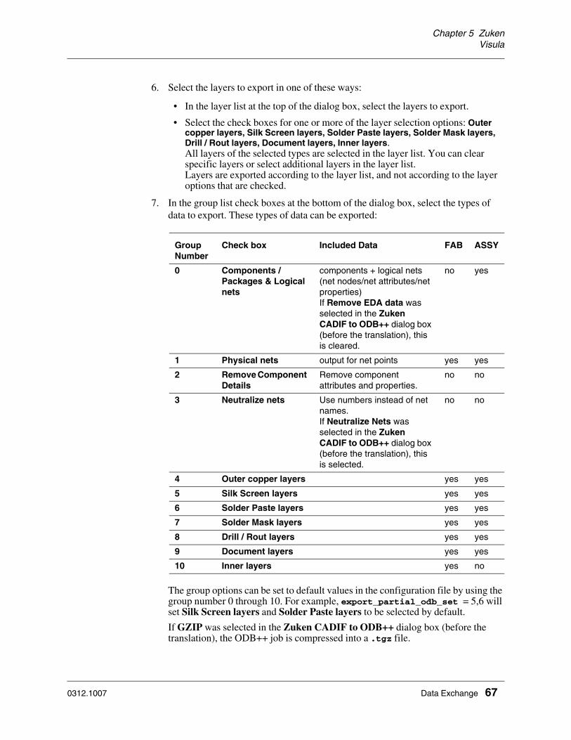
Chapter 5 ZukenVisula
6. Select the layers to export in one of these ways:
• In the layer list at the top of the dialog box, select the layers to export.
• Select the check boxes for one or more of the layer selection options: Outer copper layers, Silk Screen layers, Solder Paste layers, Solder Mask layers, Drill / Rout layers, Document layers, Inner layers.All layers of the selected types are selected in the layer list. You can clear specific layers or select additional layers in the layer list.Layers are exported according to the layer list, and not according to the layer options that are checked.
7. In the group list check boxes at the bottom of the dialog box, select the types of data to export. These types of data can be exported:
The group options can be set to default values in the configuration file by using the group number 0 through 10. For example, export_partial_odb_set = 5,6 will set Silk Screen layers and Solder Paste layers to be selected by default.
If GZIP was selected in the Zuken CADIF to ODB++ dialog box (before the translation), the ODB++ job is compressed into a .tgz file.
Group Number
Check box Included Data FAB ASSY
0 Components /Packages & Logical nets
components + logical nets (net nodes/net attributes/net properties)If Remove EDA data was selected in the Zuken CADIF to ODB++ dialog box (before the translation), this is cleared.
no yes
1 Physical nets output for net points yes yes
2 Remove Component Details
Remove component attributes and properties.
no no
3 Neutralize nets Use numbers instead of net names. If Neutralize Nets was selected in the Zuken CADIF to ODB++ dialog box (before the translation), this is selected.
no no
4 Outer copper layers yes yes
5 Silk Screen layers yes yes
6 Solder Paste layers yes yes
7 Solder Mask layers yes yes
8 Drill / Rout layers yes yes
9 Document layers yes yes
10 Inner layers yes no
0312.1007 Data Exchange 67
Chapter 5 ZukenBoard Designer (CR5000)
Board Designer (CR5000)If you have Valor Enterprise 3000 installed, you can interface directly. The procedure is fully described in Document 0307 Zuken BD Interface manual.
ODB++ output cannot be generated directly from the Board Designer application. ASCII files must be created from the Board Designer job and sent to manufacturers that use Valor Trilogy 5000.
• Zuken BD Database
• Generating ASCII Files
Zuken BD DatabaseA Board Designer archive design should be saved in two ASCII files: one file with extension .pcf or .pnf. and will have an associated footprint file with the extension .ftf located in the same directory. Board Designer has a flat file directory structure and all Board Designer files are created/saved in the same (job) directory.
PC Board ASCII File (PCF) - ASCII file describing the contents of the PC Board Database. It must be accompanied by one ftf file.
Panel ASCII File (PNF) - ASCII file describing the contents of the Panel Database.
Footprint ASCII File (FTF) - ASCII file describing the contents of the Footprint Library.
Package ASCII File (PKF) (Optional) - ASCII file describing packages used for component types.
A pcf or pnf file, together with a footprint file, contains the minimal required data to create a job.
Generating ASCII FilesTo generate the ASCII files:
• Use the standard Board Designer Input/Output module to generate ASCII data.
• If this module does not exist, the bd2val.csh script can be used to convert Board Designer jobs to ASCII. The script assumes a C shell environment running in Windows. The script path must be defined using the PATH environment variable. It is invoked in C shell.
#!/bin/csh
########################################
# BD ASCII
if ( -f $1.pcb ) then
pcout.sh -r $1.pcb -o $1.pcf
0312.1007 Data Exchange 68

Chapter 5 ZukenBoard Designer (CR5000)
partback.sh -r $1.pcb -o $1.prf
pkgback.sh -r $1.pcb -o $1.pkf
ftout.sh -r $1.pcb -o $1.ftf
mrout.sh -r $1.mrl -o $1.mrf
else if ( -f $1.pnl ) then
pnout.sh -r $1.pnl -o $1.pnf
partback.sh -r $1.pnl -o $1.prf
pkgback.sh -r $1.pnl -o $1.pkf
ftout.sh -r $1.pnl -o $1.ftf
mrout.sh -r $1.mrl -o $1.mrf
endif
0312.1007 Data Exchange 69

Chapter 5 ZukenPWS (CR3000)
PWS (CR3000)If you have Valor Enterprise 3000 installed, you can interface directly. The procedure is fully described in Document 0306 Zuken PWS Interface manual.
ODB++ output cannot be generated directly from the PWS (CR3000) application. ASCII files (described below) must be created from the PWS job and sent to manufacturers that use Valor Trilogy 5000.
Zuken PWS DatabaseThe PWS databases are binary files based on object-oriented databases. The contents of these databases can be viewed by outputting information in ASCII format.
The following three PWS ASCII files are needed for complete translation of a design, CR-3000 PWS utilities should be used to generate all required ASCII files.
Mandatory Technology file (BSF) - defines design specifications such as layers, via tables, aperture table, units and other miscellaneous data.
Component Shape Catalog File (MDF) - defines top and bottom component artworks. To differentiate between the top and bottom artworks, either a t or a b is respectively added to the artwork number.
PC Board Shape File (UDF) - defines component and feature artworks not belonging to nets. In some cases, features listed in the WDF file (see below) may also appear in this file (UDF). The translator deletes UDF duplicate features.
Optional Additional PWS ASCII file types can be created and will be used by the translation software if available.
Wiring Specifications By Signal (CCB, CCF, ECF, WDF or DRN) - defines netlist at the reference designator level. The file search sequence first checks the CCB file. If it exists, it looks no further.
If CCB does not exist, the search sequence checks in the following sequence: CCF file, ECF file, WDF file, DRN (DRC Netlist File).
Wiring Shape File (WDF) - defines all conductive features belonging to nets (pads, traces, surfaces, etc.).
PWS to ODB++ Layer Mapping File (PRM) - lists layers, which will be created in the ODB++ job, and their attributes.
The.prm file maps PWS layers and Nouns to their respective layers in the resulting ODB++ job. A Noun defines the type of feature(s) or objects found in layer.
If the.prm file is missing, default layer definitions are extracted from the.bsf file.
Translation might complete successfully with only a partial list of files, and some information may be incomplete or missing. Such a generated ODB++ file might not be suitable for Fabrication analysis.
0312.1007 Data Exchange 70

Chapter 5 ZukenCadstar
CadstarIf you have Valor Enterprise 3000 installed, you can import CADIF files as described in Document 0305 Zuken CADIF Interface manual.
Creating ODB++ OutputTo generate an ODB++ file:
1. Start the Cadstar application and load a design.
2. Select File > Export. The Export to File dialog box opens.
3. Select ODB++. The ODB++ Gateway Options dialog box opens.
4. Specify the output options:
ODB++ Generates full ODB++ output.
ODB++(X) Export to ODB++(X) generates a representation of the ODB++ format in XML format.
ODB++(X)Partial
Restricts the XML output to only the component and pad data on the outer layers. Physical nets and internal layer items are not included in the output.
0312.1007 Data Exchange 71

Chapter 5 ZukenCadstar
Remove EDAdata
Removes Component/Package information from the ODB++ job.
NeutralizeNets
Renames nets numerically.
CompressJob
Compresses the ODB++ job into one single zipped file describing the output. Otherwise, the ODB++ job is made up of several files.
5. Click OK to start the generation of ODB++.
0312.1007 Data Exchange 72
Chapter 6 AltiumDesigner (formerly Protel)
Chapter 6 Altium
This chapter discusses the following formats:
• Designer (formerly Protel)
• P-CAD
Designer (formerly Protel)If you have Valor Enterprise 3000 installed, you can interface directly. The procedure is fully described in Document 0309, Altium Designer Interface.
The complete database for this application is contained in one binary file. An Altium Designer archive design should be saved in one ASCII file with the extension pcb.
ODB++ output can be generated by two different procedures, the second procedure gives the user more control over the ODB++ output, but can only be used when the design data (PCB + Schematics) is in one project.
• Creating ODB++ Output Using Project Options
• Creating ODB++ Output Using the Output Job File Option
Creating ODB++ Output Using Project Options1. Start the Altium Designer application and load a project.
2. Select Project > Project Options. The Options for PCB Project dialog box opens.
0312.1007 Data Exchange 73
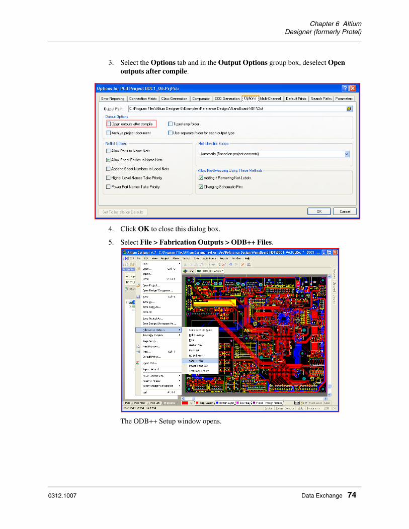
Chapter 6 AltiumDesigner (formerly Protel)
3. Select the Options tab and in the Output Options group box, deselect Open outputs after compile.
4. Click OK to close this dialog box.
5. Select File > Fabrication Outputs > ODB++ Files.
The ODB++ Setup window opens.
0312.1007 Data Exchange 74

Chapter 6 AltiumDesigner (formerly Protel)
6. Select the layers to be included in the ODB++ translation.
7. Select the Mechanical Layers to be included in the ODB++ translation.
8. In the Miscellaneous Options group, select the appropriate options:
• Select Include unconnected mid-layer pads.
• Deselect Generate DRC Rules export file (.RUL) (it is not required for ODB++ export).
• If an Embedded Board Array (panel) is exported to ODB++, you can select Export only objects inside the board outline.
• In Select the PCB layer / Board Outline that will be used to create the ODB++ 'profile' layer, specify the layer from which the ODB++ profile layer will be created.
9. Open the Plot Layers list and select layers for ODB ++ export.
All - selects all layers for ODB++ export.
None - excludes all layers from ODB++ export.
10. Click OK to start the generation of ODB++. The generated ODB++ file will be saved in the ODB directory within the Project Outputs folder.
0312.1007 Data Exchange 75

Creating ODB++ Output Using the Output Job File Option1. Start the Altium Designer application and load a design.
2. Select File > New > Output Job File. This creates a new Output Job file and places it under the Output Job Files branch of the project tree.
0312.1007 Data Exchange 76

3. Select the newly created Job from the Project Tree. The Design Explorer DXP dialog opens. The Fabrication Output section contains all supported fabrication formats.
0312.1007 Data Exchange 77

4. If ODB++ Files is not listed, select Edit > Add Fabrication Outputs > ODB++ Files.
0312.1007 Data Exchange 78

5. Check that the Data Source is the PCB document that you want to generate the Outputs for. If not, click the Data Source cell, and select the PCB document that you want to use.
0312.1007 Data Exchange 79

Chapter 6 AltiumDesigner (formerly Protel)
6. Double-click the ODB++ Files Fabrication Outputs option. The following window opens.
7. Select the layers to be included in the ODB++ translation.
8. Select the Mechanical Layers to be included in the ODB++ translation
9. In the Miscellaneous Options group, select the appropriate options:
• Select Include unconnected mid-layer pads.
• Deselect Generate DRC Rules export file (.RUL) (it is not required for ODB++ export).
• If an Embedded Board Array (panel) is exported to ODB++, you can select Export only objects inside the board outline.
• In Select the PCB layer / Board Outline that will be used to create the ODB++ 'profile' layer, specify the layer from which the ODB++ profile layer will be created.
10. Select layers for ODB ++ export.
All - Selects all layers for ODB++ export
None - Excludes all layers from ODB++ export
11. Click OK to close the dialog.
0312.1007 Data Exchange 80

Chapter 6 AltiumDesigner (formerly Protel)
12. Right-click the Job from the Project Tree and select Save from the popup menu. This saves the configuration that you have built for future use on this project.
0312.1007 Data Exchange 81

Chapter 6 AltiumP-CAD
• Right-click on the ODB++ Files Fabrication Outputs option, and select Run Output Generator. This generates the ODB++ data. The ODB++ file is saved in the ODB directory within the Project Outputs folder.
P-CADIf you have Valor Enterprise 3000 installed, you can interface directly. The procedure is fully described in Document 0308 Altium P-CAD ASCII Interface manual.
The Altium P-CAD 2002 ODB++ output provides configuration options that allow you to select which data items are to be included in the ODB++ output. Certain layers can be used in conjunction with other layers. For example, a dimension layer may be output with a Notes layer.
Although it is possible to select board layers to be included in the ODB++ output, it is recommended that all layers be output to ensure there is no missing data. When generating an ODB++ database, a directory tree structure is created with files for all appropriate design data.
0312.1007 Data Exchange 82

Chapter 6 AltiumP-CAD
Creating ODB++ OutputTo generate an ODB++ file:
1. Start the P-CAD application and load a design.
2. Select File > Export > ODB++.
3. Select the Board Layers and Drill Layers to export. Click a layer's checkbox to toggle its inclusion.
0312.1007 Data Exchange 83

Chapter 6 AltiumP-CAD
4. If necessary, specify which layers will be included with the targeted layer by right-clicking Included Layers node in the Layer Settings tree and then clicking on the desired associated layers.
5. You can specify whether to output Pads, Vias, RefDes, Type, Value, Title, and no mounting hole copper. This is done by right-clicking on an item under Layer Settings and clicking on True or False. The example at the right shows pads output selection. However, it is recommended that all data be included in ODB++ output.
NC Drill information is output as layers. Each layer contains the name of the start and end board layers for each drill range. The drill layers are generated automatically based on the user-specified pad and via styles. None of the settings for the NC Drill layers can be changed. The NC Drill information relies on the existence of all the signal/plane layers in the ODB++ database. You need to specify which of the NC Drill layers to output.
6. To display the translator log, select View Log File Upon Completion. All program messages are written to this file.
7. Click Output Location to specify the destination directory for the generated ODB++ data. Select the directory in which you wish the exported data to be stored. The output path will be updated accordingly. The selected directory must exist.
8. Click Generate to generate the output file. The ODB++ file is saved in the Output Location chosen.
For ease of communication, it is recommended that the generated ODB++ design directory be sent to manufacturers as a compressed archive file (such as tar, zip format).
0312.1007 Data Exchange 84

Chapter 7 Number One SystemsEasy-PC for Windows
Chapter 7 Number One Systems
Easy-PC for WindowsEasy-PC is the industry standard at entry level shrink wrapped market for PCB design products under US$1,000. It provides a complete front-to-back design solution of Schematics and PCB design editors, along with library create tools, a supplied library and full manufacturing outputs. As a modular system, it is highly scaleable with additional cost options and design capacity.
Creating ODB++ OutputTo generate an ODB++ file:
1. Start the Easy-PC for Windows application and load a design.
2. Select Output > ODB++ Export.
3. Select Compressed to have all data compressed into one .tgz file. Otherwise, data is output in structured folder format.
4. Click Browse to designate a location for the folder structure or the compressed file.
5. All data is compressed into one single compressed archive describing the output. If the compressed option is not selected, select Browse to designate a location where a structured folder for the various files and subfolders that describe the output will be created.
6. Click OK to start the generation of ODB++.
0312.1007 Data Exchange 85

Chapter 8 PulsonixPulsonix
Chapter 8 Pulsonix
PulsonixThe Pulsonix product serves the mid-range PCB design market, and can be used by casual users and professional users. The toolset is accessed through a graphical user interface that provides integrated Schematic Capture, PCB layout editor, graphical library creation suite and a manufacturing output feature.
Creating ODB++ OutputTo generate an ODB++ file:
1. Start the Pulsonix application and load a design.
2. Select Output > ODB++.
3. Select Compressed to have all data compressed into one .tgz file. Otherwise, data is output in structured folder format.
4. Click Browse to designate a location for the folder structure or compressed file.
5. Select Use CAM/Plot Layer Combinations to output the layer definitions used in the CAM/Plot dialog box.
6. Select Include Windows Plots to output the Windows plots defined in the CAM/Plot dialog box. If this is cleared, only plots defined for Gerber and Excellon are output as the layer combination when Use CAM/Plot Layer Combinations is selected.
7. All data is compressed into a single compressed archive describing the output. If the compressed option is not selected, select Browse to designate a location where a structured folder for the files and subfolders will be created.
0312.1007 Data Exchange 86

Chapter 8 PulsonixPulsonix
8. Click OK to start the generation of ODB++. The generated ODB++ file can be viewed with the Valor Universal Viewer (VUV) if it is installed at your site. Contact Valor for information about the VUV. Other viewers might require non-compressed format.
0312.1007 Data Exchange 87

Chapter 9 VisionicsEDWinXP
Chapter 9 Visionics
EDWinXPElectronic Design for Windows (EDWinXP) is a integrated CAD/CAE package for PCB design. An electronics design engineer can use the computerized tools provided in EDWinXP to create an electronic circuit, and to design fabricate PCBs. EDWinXP covers all stages of the design process from capturing the idea of a circuit in the form of a schematic diagram to generating documentation for manufacturing and assembly. The package includes validation tools for ensuring correctness and integrity of the designed circuits.
Creating ODB++ OutputTo export an EDWinXP project database to ODB++ format:
1. Start the EDWinXP application and load a project database.
2. Open Fabrication Manager.
3. Select Fabrication > Exports. The Fabrication Exports dialog box opens.
4. Select ODB++ Export in the tree.
5. Set the export parameters and click Export.
0312.1007 Data Exchange 88

Chapter 10 ValorEnterprise 3000
Chapter 10 Valor
Enterprise 3000Use these procedures to export a job from an internal ODB++ job database, either as ODB++ compatible data or in ODB++(X) (XML format).
• Creating ODB++ Output
• Creating ODB++(X) Output
Creating ODB++ Output1. Start the Enterprise 3000 application.
2. Select File > Export > ODB++ Job from the Engineering Toolkit. The Export Job dialog box opens:
3. In Job Name, enter the name of job to be exported.
4. In Path, enter the path to the directory in which the job is to be saved.
5. In Mode, select a mode:
• Tar gzip (.tgz) - Produces a compressed Tape Archived (tar) set of files. Tar gzip is the preferred option for optimum data transfer. A full description of the output modes can be found in Doc. 0102, Engineering Toolkit.
• Tar - Produces a combined set of files (compressed or uncompressed)
• Directory - Outputs using the same directory structure as the job. Files are copied without compression.
6. In Overwrite, specify whether you want to overwrite existing files of the same name in the defined location.
7. Click OK to start the generation of ODB++, and close the dialog.
0312.1007 Data Exchange 89

Chapter 10 ValorEnterprise 3000
Creating ODB++(X) Output1. Start the Enterprise 3000 application.
2. Select File > Export > ODB++(X) from the Engineering Toolkit. The Export ODB++(X) Job dialog box opens.
3. In Job Name, enter the name of the job to be exported.
4. In Path, enter the path to the directory in which the job is to be saved.
5. In Overwrite, specify whether you want to overwrite existing files of the same name in the defined location.
6. In Units, specify the units of measurement used in output file. (Metric (mm) or Imperial (mils))
7. In Placed Comp Only, specify whether to output all components including components having .comp_ignore attribute.
• Yes - Outputs only components that have been placed
• No - Outputs all components
8. In Mode, select a mode to define what information to export. The categories of information included with each output mode are reflected in the list in the right pane of the dialog box.
Full - Exports all the information in the job.
Partial - Exports only component and pad data on outer layers.
FAB - Exports fabrication-related data.
ASSY - Exports assembly-related data.
0312.1007 Data Exchange 90

Chapter 10 ValorEnterprise 3000
9. If you choose ASSY or FAB in the Mode box, the Level box is displayed.
In Level, you can specify how much information to export.
For ASSY, Level = 1 indicates maximum number of categories of assembly data, and Level = 6 indicates the minimum number of categories of assembly data. (Mode = ASSY, Level = 6 is identical to Partial Mode.)
For FAB, Level = 1 indicates maximum number of categories of fabrication data, and Level = 4 indicates the minimum number of categories of fabrication data.
The categories of information included for each level are reflected in the list in the right pane of the dialog box.
For a table describing the information stored in the ODB++(X) file for each level, see “Table of Export Levels for FAB and ASSY Modes” on page 11.
10. In Layers, specify the layers to export.
Default - System determines the layers
All - Exports all layers.
None - No layers are exported
Select - Select for export each layer individually (by clicking on the checkbox). After choosing Select, all layers will become selected. Deselect any layer you do not want to export.
11. In Suppress Data, specify whether data is to be suppressed.
No - Exports all data
Yes - Does not export blank data.
0312.1007 Data Exchange 91

Appendix A Thermal Model
Appendix A Thermal Model
Depending on the PCB application, to generate accurate board data, you are required to use of a Thermal Model to explicitly define these shapes.
• Structure of a Thermal Model File
• BNF (Backus-Naur Form) of Rules
• Sample Thermal Model File
Structure of a Thermal Model FileThe Thermal Model File includes a units definition followed by any number of models. Lines preceded by a ‘#’ character are treated as comments and ignored.
.units < inch | mm > - The units definition specifies the measurement units that will be used for the models. Legal values are inch and mm.
.model <name> - Each model begins with the model directive. The name is limited to 64 characters that may include letters, digits, and the following symbols:
For an example of a Thermal Model file, see “Sample Thermal Model File” on page 93.
BNF (Backus-Naur Form) of RulesThe model directive is followed by a sequence of rules.
<rule> ::= <condition> : <derivation>
If the condition is met, then the thermal shape definition described in the derivation is used for the pad. The first match is used.
<condition> ::= <type> { <equation> }
<type> ::= PIN | VIA | geometry_name | 'geometry_name'
<equation> ::= [D|C] ['<' | '<=' | '=' | '>' | '>='] <value>
The padstack can be compared by its type, either PIN or VIA, or by its padstack name. The padstack name may be enclosed in quotes to accommodate padstacks named PIN or VIA.
Name Symbol
dash -
underscore _
period .
plus +
0312.1007 Data Exchange 92

Appendix A Thermal Model
The padstack can also be compared based on drill size (represented by the ‘D’ in the equation), or by clearance size (represented by the ‘C’ in the equation).
<derivation> ::= NULL | '<sym_name>' | <set_values>
<sym_name> ::= any ODB++ standard or semi-standard name
The shape can be defined directly by providing the symbol name; or the parameters for the symbol can be derived based on the drill and clearance sizes (represented by ‘D’ and ‘C’, respectively).
The ‘NULL’ shape can be used to produce direct connects.
<set_values> ::= <id> <od> <tie> <num_ties> <angle>
<oshape> <ishape> <style>
<id>::=<diam_value>
<od>::=<diam_value>
<diam_value>::=[ C | D ] [ "+" | "-" ] [<value>]
The inner diameter is represented by <id> and the outer diameter is represented by <od>.
<tie> ::= <value>
<num_ties> ::= <value>
<tie> is the size of the tie and <num_ties> is the number of ties.
<angle> ::= <value>
<angle> represents the start angle for the first tie in degrees.
<oshape> ::= R | S | C
<ishape> ::= R | S | C
<style> ::= R | S
• <oshape> represents the outer shape. It can be either Round (‘R’), Square (‘S’) or the same shape as the clearance (‘C’).
• <ishape> represents the inner shape. It can be either Round (‘R’), Square (‘S’) or the same shape as the clearance (‘C’).
• <style> can be Rounded (‘R’) or Squared (‘S’).
Sample Thermal Model File.units inch.model allegro_model# direct replacement of symbols
# replace the padflash named "TH05" with a round clearance of #5 mils. TH05 : 'r5'
# replace the padflash named "T165X145X20X45" with a square thermal# with an outer diameter of 165 mils, inner diameter of 145 mils# with four ties each of 20 mils, first starting at 45 degrees.T165X145X20X45 : 'ths165x145x45x4x20'
0312.1007 Data Exchange 93

Appendix A Thermal Model
# replace the padflash named "5MIL" with a direct connection5MIL : 'null'
# calculated values
# Place a direct connect for all VIA padsVIA : NULL
# For pins with a clearance less than or equal to 45 mils# place a rounded thermal with outer diameter the size of the clearance# inner diameter 20 mils smaller, # 4 ties of 20 mil starting at 45 degrees# outer and inner diameters shaped as the clearancePIN C<=45 : C C-20 15 4 45 C C R
0312.1007 Data Exchange 94