
Data and Non-volatile Program Memory Endurance: 10,000 ...
176
1477D–AVR–06/03 Features • High-performance, Low-power AVR ® 8-bit Microcontroller • RISC Architecture – 118 Powerful Instructions – Most Single Clock Cycle Execution – 32 x 8 General Purpose Working Registers – Fully Static Operation – Up to 16 MIPS Throughput at 16 MHz • Data and Non-volatile Program Memory – 2K Bytes of In-System Programmable Program Memory Flash Endurance: 10,000 Write/Erase Cycles – 128 Bytes of In-System Programmable EEPROM Endurance: 100,000 Write/Erase Cycles – 128 Bytes Internal SRAM – Programming Lock for Flash Program and EEPROM Data Security • Peripheral Features – 8-bit Timer/Counter with Separate Prescaler – 8-bit High-speed Timer with Separate Prescaler 2 High Frequency PWM Outputs with Separate Output Compare Registers Non-overlapping Inverted PWM Output Pins – Universal Serial Interface with Start Condition Detector – 10-bit ADC 11 Single Ended Channels 8 Differential ADC Channels 7 Differential ADC Channel Pairs with Programmable Gain (1x, 20x) – On-chip Analog Comparator – External Interrupt – Pin Change Interrupt on 11 Pins – Programmable Watchdog Timer with Separate On-chip Oscillator • Special Microcontroller Features – Low Power Idle, Noise Reduction, and Power-down Modes – Power-on Reset and Programmable Brown-out Detection – External and Internal Interrupt Sources – In-System Programmable via SPI Port – Internal Calibrated RC Oscillator • I/O and Packages – 20-lead PDIP/SOIC: 16 Programmable I/O Lines • Operating Voltages – 2.7V - 5.5V for ATtiny26L – 4.5V - 5.5V for ATtiny26 • Speed Grades – 0 - 8 MHz for ATtiny26L – 0 - 16 MHz for ATtiny26 8-bit Microcontroller with 2K Bytes Flash ATtiny26 ATtiny26L Preliminary Rev. 1477D–AVR–06/03
Transcript of Data and Non-volatile Program Memory Endurance: 10,000 ...

1477D–AVR–06/03
8-bit Microcontroller with 2K Bytes Flash
ATtiny26ATtiny26L
Preliminary
Rev. 1477D–AVR–06/03
Features• High-performance, Low-power AVR ® 8-bit Microcontroller• RISC Architecture
– 118 Powerful Instructions – Most Single Clock Cycle Execution– 32 x 8 General Purpose Working Registers– Fully Static Operation– Up to 16 MIPS Throughput at 16 MHz
• Data and Non-volatile Program Memory– 2K Bytes of In-System Programmable Program Memory Flash
Endurance: 10,000 Write/Erase Cycles– 128 Bytes of In-System Programmable EEPROM
Endurance: 100,000 Write/Erase Cycles– 128 Bytes Internal SRAM– Programming Lock for Flash Program and EEPROM Data Security
• Peripheral Features– 8-bit Timer/Counter with Separate Prescaler– 8-bit High-speed Timer with Separate Prescaler
2 High Frequency PWM Outputs with Separate Output Compare RegistersNon-overlapping Inverted PWM Output Pins
– Universal Serial Interface with Start Condition Detector– 10-bit ADC
11 Single Ended Channels8 Differential ADC Channels7 Differential ADC Channel Pairs with Programmable Gain (1x, 20x)
– On-chip Analog Comparator– External Interrupt– Pin Change Interrupt on 11 Pins– Programmable Watchdog Timer with Separate On-chip Oscillator
• Special Microcontroller Features– Low Power Idle, Noise Reduction, and Power-down Modes– Power-on Reset and Programmable Brown-out Detection– External and Internal Interrupt Sources– In-System Programmable via SPI Port– Internal Calibrated RC Oscillator
• I/O and Packages– 20-lead PDIP/SOIC: 16 Programmable I/O Lines
• Operating Voltages– 2.7V - 5.5V for ATtiny26L– 4.5V - 5.5V for ATtiny26
• Speed Grades– 0 - 8 MHz for ATtiny26L– 0 - 16 MHz for ATtiny26
1
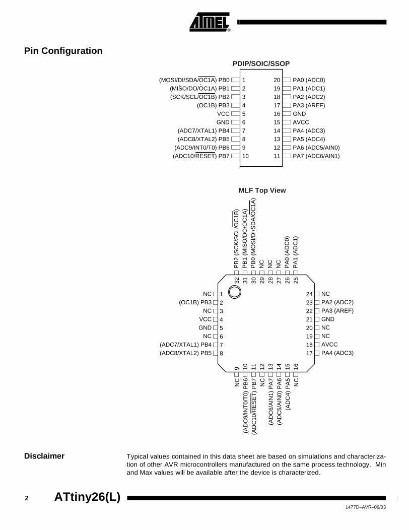
Pin Configuration
Disclaimer Typical values contained in this data sheet are based on simulations and characteriza-tion of other AVR microcontrollers manufactured on the same process technology. Minand Max values will be available after the device is characterized.
12345678910
20191817161514131211
(MOSI/DI/SDA/OC1A) PB0 (MISO/DO/OC1A) PB1(SCK/SCL/OC1B) PB2
(OC1B) PB3VCCGND
(ADC7/XTAL1) PB4(ADC8/XTAL2) PB5
(ADC9/INT0/T0) PB6 (ADC10/RESET) PB7
PA0 (ADC0)PA1 (ADC1) PA2 (ADC2)PA3 (AREF)GNDAVCCPA4 (ADC3)PA5 (ADC4)PA6 (ADC5/AIN0)PA7 (ADC6/AIN1)
PDIP/SOIC/SSOP
12345678
2423222120191817
32 31 30 29 28 27 26 25
9 10 11 12 13 14 15 16
MLF Top View
NC(OC1B) PB3
NCVCCGND
NC(ADC7/XTAL1) PB4(ADC8/XTAL2) PB5
NCPA2 (ADC2)PA3 (AREF)GNDNCNCAVCCPA4 (ADC3)
NC
(AD
C9/
INT
0/T
0) P
B6
(AD
C10
/RE
SE
T)
PB
7N
C(A
DC
6/A
IN1)
PA
7 (
AD
C5/
AIN
0) P
A6
(AD
C4)
PA
5N
C
PB
2 (S
CK
/SC
L/O
C1B
)P
B1
(MIS
O/D
O/O
C1A
)P
B0
(MO
SI/D
I/SD
A/O
C1A
) N
CN
CN
CP
A0
(AD
C0)
PA
1 (A
DC
1)
2 ATtiny26(L) 1477D–AVR–06/03
ATtiny26(L)
Description The ATtiny26(L) is a low-power CMOS 8-bit microcontroller based on the AVRenhanced RISC architecture. By executing powerful instructions in a single clock cycle,the ATtiny26(L) achieves throughputs approaching 1 MIPS per MHz allowing the systemdesigner to optimize power consumption versus processing speed.
The AVR core combines a rich instruction set with 32 general purpose working registers.All the 32 registers are directly connected to the Arithmetic Logic Unit (ALU), allowingtwo independent registers to be accessed in one single instruction executed in one clockcycle. The resulting architecture is more code efficient while achieving throughputs up toten times faster than conventional CISC microcontrollers. The ATtiny26(L) has a highprecision ADC with up to 11 single ended channels and 8 differential channels. Sevendifferential channels have an optional gain of 20x. Four out of the seven differentialchannels, which have the optional gain, can be used at the same time. The ATtiny26(L)also has a high frequency 8-bit PWM module with two independent outputs. Two of thePWM outputs have inverted non-overlapping output pins ideal for synchronous rectifica-tion. The Universal Serial Interface of the ATtiny26(L) allows efficient softwareimplementation of TWI (Two-wire Serial Interface) or SM-bus interface. These featuresallow for highly integrated battery charger and lighting ballast applications, low-end ther-mostats, and firedetectors, among other applications.
The ATtiny26(L) provides 2K bytes of Flash, 128 bytes EEPROM, 128 bytes SRAM, upto 16 general purpose I/O lines, 32 general purpose working registers, two 8-bitTimer/Counters, one with PWM outputs, internal and external Oscillators, internal andexternal interrupts, programmable Watchdog Timer, 11-channel, 10-bit Analog to DigitalConverter with two differential voltage input gain stages, and four software selectablepower saving modes. The Idle mode stops the CPU while allowing the Timer/Countersand interrupt system to continue functioning. The ATtiny26(L) also has a dedicated ADCNoise Reduction mode for reducing the noise in ADC conversion. In this sleep mode,only the ADC is functioning. The Power-down mode saves the register contents butfreezes the oscillators, disabling all other chip functions until the next interrupt or hard-ware reset. The Standby mode is the same as the Power-down mode, but externaloscillators are enabled. The wakeup or interrupt on pin change features enable theATtiny26(L) to be highly responsive to external events, still featuring the lowest powerconsumption while in the Power-down mode.
The device is manufactured using Atmel’s high density non-volatile memory technology.By combining an enhanced RISC 8-bit CPU with Flash on a monolithic chip, theATtiny26(L) is a powerful microcontroller that provides a highly flexible and cost effec-tive solution to many embedded control applications.
The ATtiny26(L) AVR is supported with a full suite of program and system developmenttools including: Macro assemblers, program debugger/simulators, In-circuit emulators,and evaluation kits.
31477D–AVR–06/03

Block Diagram Figure 1. The ATtiny26(L) Block Diagram
WATCHDOGTIMER
MCU CONTROLREGISTER
UNIVERSALSERIAL
INTERFACE
TIMER/COUNTER0
DATA DIR.REG.PORT A
DATA REGISTERPORT A
PROGRAMMINGLOGIC
TIMING ANDCONTROL
TIMER/COUNTER1
MCU STATUSREGISTER
PORT A DRIVERS
PA0-PA7
VCC
GND
+ -
AN
ALO
GC
OM
PA
RA
TO
R
8-BIT DATA BUS
ADC
ISP INTERFACE
INTERRUPTUNIT
EEPROM
INTERNALOSCILLATOR
OSCILLATORS
CALIBRATEDOSCILLATOR
INTERNAL
DATA DIR.REG.PORT B
DATA REGISTERPORT B
PORT B DRIVERS
PB0-PB7
PROGRAMCOUNTER
STACKPOINTER
PROGRAMFLASH SRAM
GENERALPURPOSE
REGISTERS
INSTRUCTIONREGISTER
INSTRUCTIONDECODER
STATUSREGISTER
Z
YX
ALUCONTROL
LINES
AVCC
4 ATtiny26(L) 1477D–AVR–06/03

ATtiny26(L)
Pin Descriptions
VCC Digital supply voltage pin.
GND Digital ground pin.
AVCC AVCC is the supply voltage pin for Port A and the A/D Converter (ADC). It should beexternally connected to VCC, even if the ADC is not used. If the ADC is used, it should beconnected to VCC through a low-pass filter. See page 77 for details on operating of theADC.
Port A (PA7..PA0) Port A is an 8-bit general purpose I/O port. PA7..PA0 are all I/O pins that can provideinternal pull-ups (selected for each bit). Port A has alternate functions as analog inputsfor the ADC and analog comparator and pin change interrupt as described in “AlternatePort Functions” on page 95.
Port B (PB7..PB0) Port B is an 8-bit general purpose I/O port. PB6..0 are all I/O pins that can provide inter-nal pull-ups (selected for each bit). PB7 is an I/O pin if not used as the reset. To use pinPB7 as an I/O pin, instead of RESET pin, program (“0”) RSTDISBL Fuse. Port B hasalternate functions for the ADC, clocking, timer counters, USI, SPI programming, andpin change interrupt as described in “Alternate Port Functions” on page 95.
An External Reset is generated by a low level on the PB7/RESET pin. Reset pulseslonger than 50 ns will generate a reset, even if the clock is not running. Shorter pulsesare not guaranteed to generate a reset.
XTAL1 Input to the inverting oscillator amplifier and input to the internal clock operating circuit.
XTAL2 Output from the inverting oscillator amplifier.
51477D–AVR–06/03

Architectural Overview
The fast-access Register File concept contains 32 x 8-bit general purpose working reg-isters with a single clock cycle access time. This means that during one single clockcycle, one ALU (Arithmetic Logic Unit) operation is executed. Two operands are outputfrom the Register File, the operation is executed, and the result is stored back in theRegister File – in one clock cycle.
Six of the 32 registers can be used as 16-bit pointers for indirect memory access. Thesepointers are called the X-, Y-, and Z-pointers, and they can address the Register Fileand the Flash program memory.
Figure 2. The ATtiny26(L) AVR Enhanced RISC Architecture
The ALU supports arithmetic and logic functions between registers or between a con-stant and a register. Single register operations are also executed in the ALU. Figure 2shows the ATtiny26(L) AVR Enhanced RISC microcontroller architecture. In addition tothe register operation, the conventional memory addressing modes can be used on theRegister File as well. This is enabled by the fact that the Register File is assigned the 32lowermost Data Space addresses ($00 - $1F), allowing them to be accessed as thoughthey were ordinary memory locations.
The I/O memory space contains 64 addresses for CPU peripheral functions as ControlRegisters, Timer/Counters, A/D Converters, and other I/O functions. The I/O Memorycan be accessed directly, or as the Data Space locations following those of the RegisterFile, $20 - $5F.
The AVR uses a Harvard architecture concept with separate memories and buses forprogram and data memories. The program memory is accessed with a two stage
1024 x 16ProgramFLASH
InstructionRegister
InstructionDecoder
ProgramCounter
Control Lines
32 x 8GeneralPurpose
Registers
ALU
Dire
ct A
ddre
ssin
g
Indi
rect
Add
ress
ing
Statusand Test
ControlRegisters
InterruptUnit
2 x 8-bitTimer/Counter
UniversalSerial Interface
WatchdogTimer
AnalogComparator
I/O Lines
8-bit Data Bus
ISP Unit
ADC128 x 8SRAM
128 byteEEPROM
6 ATtiny26(L) 1477D–AVR–06/03
ATtiny26(L)
pipelining. While one instruction is being executed, the next instruction is pre-fetchedfrom the program memory. This concept enables instructions to be executed in everyclock cycle. The program memory is In-System programmable Flash memory.
With the relative jump and relative call instructions, the whole address space is directlyaccessed. All AVR instructions have a single 16-bit word format, meaning that everyprogram memory address contains a single 16-bit instruction.
During interrupts and subroutine calls, the return address program counter (PC) isstored on the Stack. The Stack is effectively allocated in the general data SRAM, andconsequently the stack size is only limited by the total SRAM size and the usage of theSRAM. All user programs must initialize the SP in the reset routine (before subroutinesor interrupts are executed). The 8-bit Stack Pointer SP is read/write accessible in the I/Ospace. For programs written in C, the stack size must be declared in the linker file. Referto the C user guide for more information.
The 128 bytes data SRAM can be easily accessed through the five different addressingmodes supported in the AVR architecture.
The memory spaces in the AVR architecture are all linear and regular memory maps.
The I/O memory space contains 64 addresses for CPU peripheral functions as ControlRegisters, Timer/Counters, and other I/O functions. The memory spaces in the AVRarchitecture are all linear and regular memory maps.
A flexible interrupt module has its control registers in the I/O space with an additionalGlobal Interrupt Enable bit in the Status Register. All the different interrupts have a sep-arate Interrupt Vector in the Interrupt Vector table at the beginning of the programmemory. The different interrupts have priority in accordance with their Interrupt Vectorposition. The lower the Interrupt Vector address, the higher the priority.
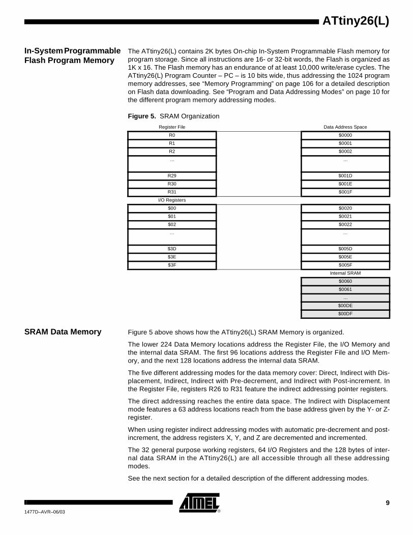
General Purpose Register File
Figure 3 shows the structure of the 32 general purpose working registers in the CPU.
Figure 3. AVR CPU General Purpose Working Registers
7 0 Addr.
R0 $00
R1 $01
R2 $02
…
R13 $0D
General R14 $0E
Purpose R15 $0F
Working R16 $10
Registers R17 $11
…
R26 $1A X-register Low Byte
R27 $1B X-register High Byte
R28 $1C Y-register Low Byte
R29 $1D Y-register High Byte
R30 $1E Z-register Low Byte
R31 $1F Z-register High Byte
71477D–AVR–06/03

All of the register operating instructions in the instruction set have direct and single cycleaccess to all registers. The only exceptions are the five constant arithmetic and logicinstructions SBCI, SUBI, CPI, ANDI, and ORI between a constant and a register, andthe LDI instruction for load immediate constant data. These instructions apply to thesecond half of the registers in the Register File – R16..R31. The general SBC, SUB, CP,AND, and OR, and all other operations between two registers or on a single registerapply to the entire Register File.
As shown in Figure 3, each register is also assigned a data memory address, mappingthem directly into the first 32 locations of the user Data Space. Although not being phys-ically implemented as SRAM locations, this memory organization provides flexibility inaccess of the registers, as the X-, Y-, and Z-registers can be set to index any register inthe file.
X-register, Y-register, and Z-register
The registers R26..R31 have some added functions to their general purpose usage.These registers are address pointers for indirect addressing of the Data Space. Thethree indirect address registers X, Y, and Z are defined as:
Figure 4. X-, Y-, and Z-register
In the different addressing modes, these address registers have functions as fixed dis-placement, automatic increment and decrement (see the descriptions for the differentinstructions).
ALU – Arithmetic Logic Unit
The high-performance AVR ALU operates in direct connection with all 32 general pur-pose working registers. Within a single clock cycle, ALU operations between registers inthe Register File are executed. The ALU operations are divided into three main catego-ries – Arithmetic, Logical, and Bit-functions.
15 0
X-register 7 0 7 0
R27 ($1B) R26 ($1A)
15 0
Y-register 7 0 7 0
R29 ($1D) R28 ($1C)
15 0
Z-register 7 0 7 0
R31 ($1F) R30 ($1E)
8 ATtiny26(L) 1477D–AVR–06/03
ATtiny26(L)
In-System Programmable Flash Program Memory
The ATtiny26(L) contains 2K bytes On-chip In-System Programmable Flash memory forprogram storage. Since all instructions are 16- or 32-bit words, the Flash is organized as1K x 16. The Flash memory has an endurance of at least 10,000 write/erase cycles. TheATtiny26(L) Program Counter – PC – is 10 bits wide, thus addressing the 1024 programmemory addresses, see “Memory Programming” on page 106 for a detailed descriptionon Flash data downloading. See “Program and Data Addressing Modes” on page 10 forthe different program memory addressing modes.
Figure 5. SRAM Organization
SRAM Data Memory Figure 5 above shows how the ATtiny26(L) SRAM Memory is organized.
The lower 224 Data Memory locations address the Register File, the I/O Memory andthe internal data SRAM. The first 96 locations address the Register File and I/O Mem-ory, and the next 128 locations address the internal data SRAM.
The five different addressing modes for the data memory cover: Direct, Indirect with Dis-placement, Indirect, Indirect with Pre-decrement, and Indirect with Post-increment. Inthe Register File, registers R26 to R31 feature the indirect addressing pointer registers.
The direct addressing reaches the entire data space. The Indirect with Displacementmode features a 63 address locations reach from the base address given by the Y- or Z-register.
When using register indirect addressing modes with automatic pre-decrement and post-increment, the address registers X, Y, and Z are decremented and incremented.
The 32 general purpose working registers, 64 I/O Registers and the 128 bytes of inter-nal data SRAM in the ATtiny26(L) are all accessible through all these addressingmodes.
See the next section for a detailed description of the different addressing modes.
Register File Data Address Space
R0 $0000
R1 $0001
R2 $0002
... ...
R29 $001D
R30 $001E
R31 $001F
I/O Registers
$00 $0020
$01 $0021
$02 $0022
… …
$3D $005D
$3E $005E
$3F $005F
Internal SRAM
$0060
$0061
...
$00DE
$00DF
91477D–AVR–06/03
Program and Data Addressing Modes
The ATtiny26(L) AVR Enhanced RISC microcontroller supports powerful and efficientaddressing modes for access to the Flash program memory, SRAM, Register File, andI/O Data memory. This section describes the different addressing modes supported bythe AVR architecture. In the figures, OP means the operation code part of the instructionword. To simplify, not all figures show the exact location of the addressing bits.
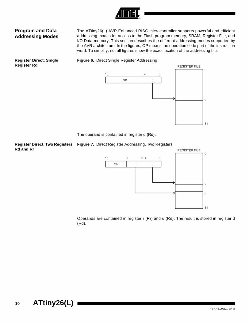
Register Direct, Single Register Rd
Figure 6. Direct Single Register Addressing
The operand is contained in register d (Rd).
Register Direct, Two Registers Rd and Rr
Figure 7. Direct Register Addressing, Two Registers
Operands are contained in register r (Rr) and d (Rd). The result is stored in register d(Rd).
10 ATtiny26(L) 1477D–AVR–06/03

ATtiny26(L)
I/O Direct Figure 8. I/O Direct Addressing
Operand address is contained in 6 bits of the instruction word. n is the destination orsource register address.
Data Direct Figure 9. Direct Data Addressing
A 16-bit Data Address is contained in the 16 LSBs of a two-word instruction. Rd/Rrspecify the destination or source register.
Data Indirect with Displacement
Figure 10. Data Indirect with Displacement
OP Rr/Rd
1631
15 0
16 LSBs
$0000
$00DF
20 19
Data Space
Data Space$0000
$00DF
Y OR Z - REGISTER
OP an
0
05610
15
15
111477D–AVR–06/03
Operand address is the result of the Y- or Z-register contents added to the address con-tained in 6 bits of the instruction word.
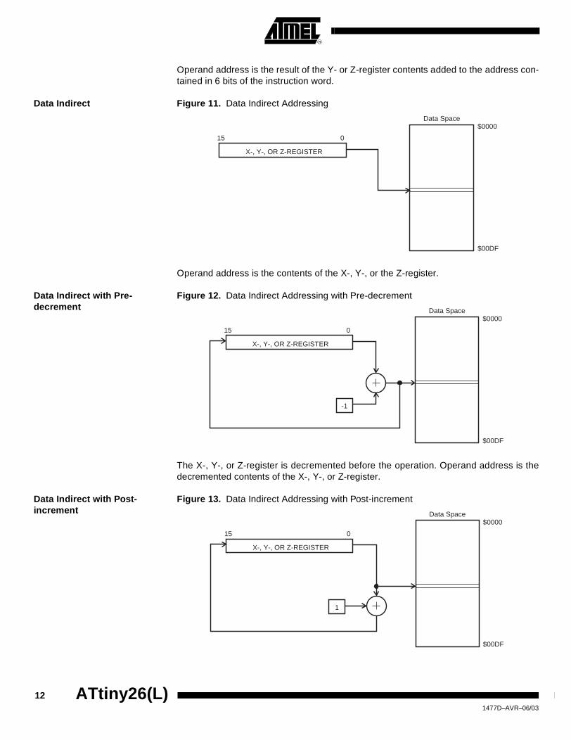
Data Indirect Figure 11. Data Indirect Addressing
Operand address is the contents of the X-, Y-, or the Z-register.
Data Indirect with Pre-decrement
Figure 12. Data Indirect Addressing with Pre-decrement
The X-, Y-, or Z-register is decremented before the operation. Operand address is thedecremented contents of the X-, Y-, or Z-register.
Data Indirect with Post-increment
Figure 13. Data Indirect Addressing with Post-increment
Data Space$0000
$00DF
X-, Y-, OR Z-REGISTER
015
Data Space$0000
$00DF
X-, Y-, OR Z-REGISTER
015
-1
Data Space$0000
$00DF
X-, Y-, OR Z-REGISTER
015
1
12 ATtiny26(L) 1477D–AVR–06/03
ATtiny26(L)
The X-, Y-, or Z-register is incremented after the operation. Operand address is the con-tent of the X-, Y-, or Z-register prior to incrementing.
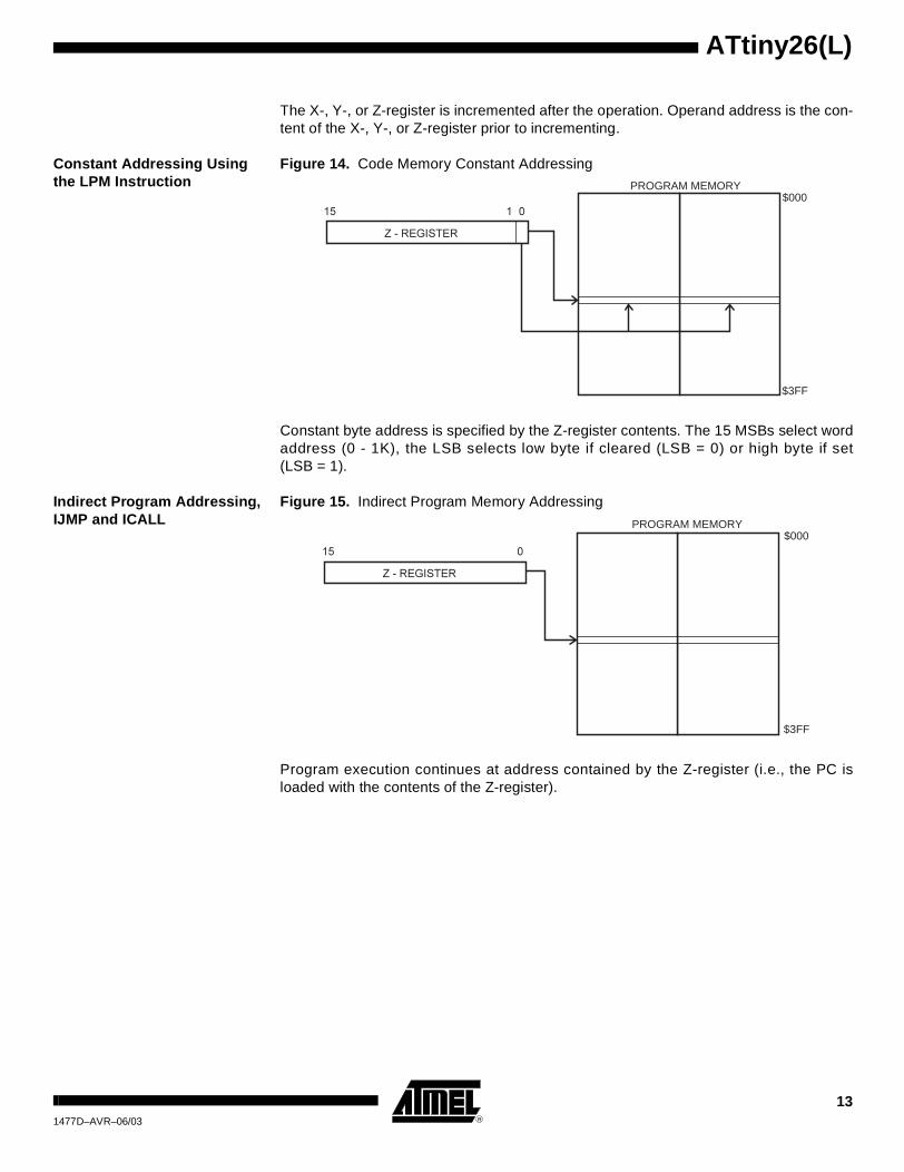
Constant Addressing Using the LPM Instruction
Figure 14. Code Memory Constant Addressing
Constant byte address is specified by the Z-register contents. The 15 MSBs select wordaddress (0 - 1K), the LSB selects low byte if cleared (LSB = 0) or high byte if set(LSB = 1).
Indirect Program Addressing, IJMP and ICALL
Figure 15. Indirect Program Memory Addressing
Program execution continues at address contained by the Z-register (i.e., the PC isloaded with the contents of the Z-register).
$3FF
$000PROGRAM MEMORY
$3FF
$000PROGRAM MEMORY
131477D–AVR–06/03

Relative Program Addressing, RJMP and RCALL
Figure 16. Relative Program Memory Addressing
Program execution continues at address PC + k + 1. The relative address k is from-2048 to 2047.
EEPROM Data Memory The ATtiny26(L) contains 128 bytes of data EEPROM memory. It is organized as a sep-arate data space, in which single bytes can be read and written. The EEPROM has anendurance of at least 100,000 write/erase cycles per location. The access between theEEPROM and the CPU is described on “EEPROM Read/Write Access” on page 60specifying the EEPROM Address Registers, the EEPROM Data Register, and theEEPROM Control Register.
For the programming of the EEPROM See “Memory Programming” on page 106.
$3FF
$000PROGRAM MEMORY
+1
14 ATtiny26(L) 1477D–AVR–06/03
ATtiny26(L)
Memory Access Times and Instruction Execution Timing
This section describes the general access timing concepts for instruction execution andinternal memory access.
The AVR CPU is driven by the System Clock Ø, directly generated from the externalclock crystal for the chip. No internal clock division is used.
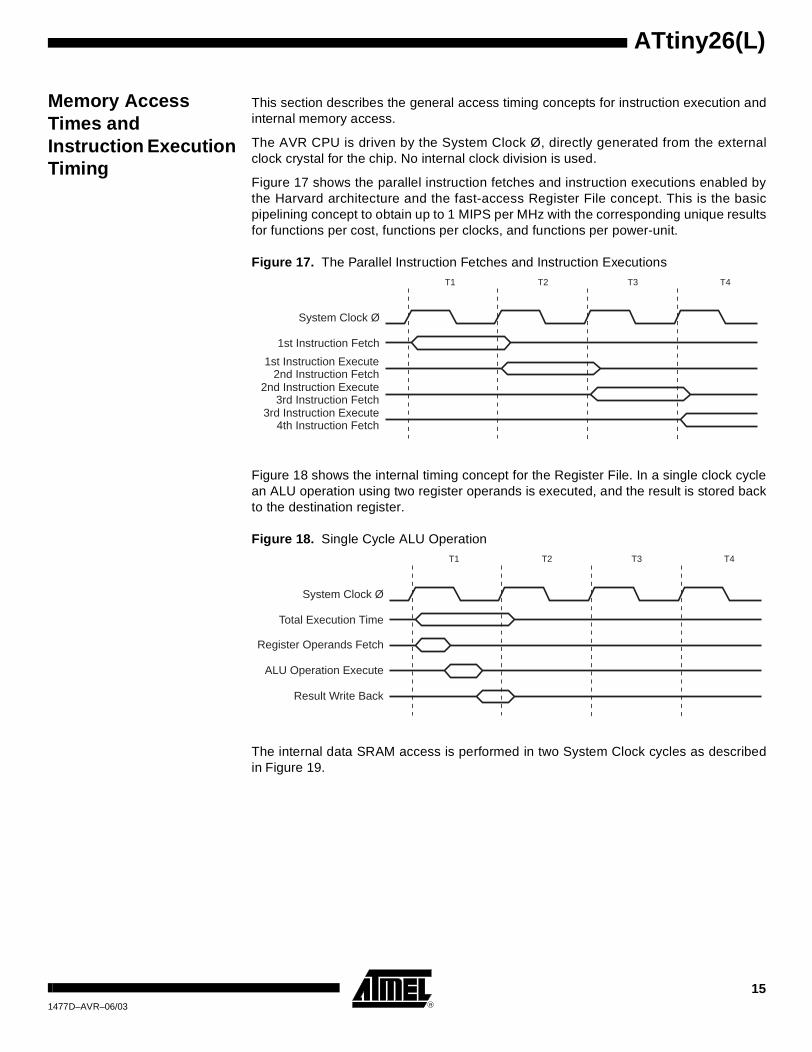
Figure 17 shows the parallel instruction fetches and instruction executions enabled bythe Harvard architecture and the fast-access Register File concept. This is the basicpipelining concept to obtain up to 1 MIPS per MHz with the corresponding unique resultsfor functions per cost, functions per clocks, and functions per power-unit.
Figure 17. The Parallel Instruction Fetches and Instruction Executions
Figure 18 shows the internal timing concept for the Register File. In a single clock cyclean ALU operation using two register operands is executed, and the result is stored backto the destination register.
Figure 18. Single Cycle ALU Operation
The internal data SRAM access is performed in two System Clock cycles as describedin Figure 19.
System Clock Ø
1st Instruction Fetch
1st Instruction Execute2nd Instruction Fetch
2nd Instruction Execute3rd Instruction Fetch
3rd Instruction Execute4th Instruction Fetch
T1 T2 T3 T4
System Clock Ø
Total Execution Time
Register Operands Fetch
ALU Operation Execute
Result Write Back
T1 T2 T3 T4
151477D–AVR–06/03

Figure 19. On-chip Data SRAM Access Cycles
System Clock Ø
WR
RD
Data
Data
Address Address
T1 T2 T3 T4
Prev. Address
Rea
dW
rite
16 ATtiny26(L) 1477D–AVR–06/03

ATtiny26(L)
I/O Memory The I/O space definition of the ATtiny26(L) is shown in Table 1
Table 1. ATtiny26(L) I/O Space(1)
Address Hex Name Function
$3F ($5F) SREG Status Register
$3D ($5D) SP Stack Pointer
$3B ($5B) GIMSK General Interrupt Mask Register
$3A ($5A) GIFR General Interrupt Flag Register
$39 ($59) TIMSK Timer/Counter Interrupt Mask Register
$38 ($58) TIFR Timer/Counter Interrupt Flag Register
$35 ($55) MCUCR MCU Control Register
$34 ($54) MCUSR MCU Status Register
$33 ($53) TCCR0 Timer/Counter0 Control Register
$32 ($52) TCNT0 Timer/Counter0 (8-bit)
$31 ($51) OSCCAL Oscillator Calibration Register
$30 ($50) TCCR1A Timer/Counter1 Control Register A
$2F ($4F) TCCR1B Timer/Counter1 Control Register B
$2E ($4E) TCNT1 Timer/Counter1 (8-bit)
$2D ($4D) OCR1A Timer/Counter1 Output Compare Register A
$2C ($4C) OCR1B Timer/Counter1 Output Compare Register B
$2B ($4B) OCR1C Timer/Counter1 Output Compare Register C
$29 ($29) PLLCSR PLL Control and Status Register
$21 ($41) WDTCR Watchdog Timer Control Register
$1E ($3E) EEAR EEPROM Address Register
$1D ($3D) EEDR EEPROM Data Register
$1C ($3C) EECR EEPROM Control Register
$1B ($3B) PORTA Data Register, Port A
$1A ($3A) DDRA Data Direction Register, Port A
$19 ($39) PINA Input Pins, Port A
$18 ($38) PORTB Data Register, Port B
$17 ($37) DDRB Data Direction Register, Port B
$16 ($36) PINB Input Pins, Port B
$0F ($2F) USIDR Universal Serial Interface Data Register
$0E ($2E) USISR Universal Serial Interface Status Register
$0D ($2D) USICR Universal Serial Interface Control Register
$08 ($28) ACSR Analog Comparator Control and Status Register
$07 ($27) ADMUX ADC Multiplexer Select Register
171477D–AVR–06/03

Note: 1. Reserved and unused locations are not shown in the table.
All ATtiny26(L) I/O and peripheral registers are placed in the I/O space. The I/O loca-tions are accessed by the IN and OUT instructions transferring data between the 32general purpose working registers and the I/O space. I/O Registers within the addressrange $00 - $1F are directly bit-accessible using the SBI and CBI instructions. In theseregisters, the value of single bits can be checked by using the SBIS and SBIC instruc-tions. Refer to the instruction set chapter for more details. For compatibility with futuredevices, reserved bits should be written zero if accessed. Reserved I/O memoryaddresses should never be written.
The I/O and peripheral control registers are explained in the following sections.
Status Register – SREG The AVR Status Register – SREG – at I/O space location $3F is defined as:
• Bit 7 – I: Global Interrupt Enable
The Global Interrupt Enable bit must be set (one) for the interrupts to be enabled. Theindividual interrupt enable control is then performed in the Interrupt Mask Registers –GIMSK and TIMSK. If the Global Interrupt Enable Register is cleared (zero), none of theinterrupts are enabled independent of the GIMSK and TIMSK values. The I-bit is clearedby hardware after an interrupt has occurred, and is set by the RETI instruction to enablesubsequent interrupts. The I-bit can also be set and cleared by the application with theSEI and CLI instructions, as described in the instruction set reference.
• Bit 6 – T: Bit Copy Storage
The Bit Copy instructions BLD (Bit LoaD) and BST (Bit STore) use the T-bit as sourceand destination for the operated bit. A bit from a register in the Register File can be cop-ied into T by the BST instruction, and a bit in T can be copied into a bit in a register in theRegister File by the BLD instruction.
• Bit 5 – H: Half Carry Flag
The Half Carry Flag H indicates a Half Carry in some arithmetic operations. See theInstruction Set Description for detailed information.
• Bit 4 – S: Sign Bit, S = N ⊕ V
The S-bit is always an exclusive or between the Negative Flag N and the Two’s Comple-ment Overflow Flag V. See the Instruction Set Description for detailed information.
• Bit 3 – V: Two’s Complement Overflow Flag
The Two’s Complement Overflow Flag V supports two’s complement arithmetics. Seethe Instruction Set Description for detailed information.
$06($26) ADCSR ADC Control and Status Register
$05($25) ADCH ADC Data Register High
$04($24) ADCL ADC Data Register Low
Table 1. ATtiny26(L) I/O Space(1) (Continued)
Address Hex Name Function
Bit 7 6 5 4 3 2 1 0
$3F ($5F) I T H S V N Z C SREG
Read/Write R/W R/W R/W R/W R/W R/W R/W R/W
Initial Value 0 0 0 0 0 0 0 0
18 ATtiny26(L) 1477D–AVR–06/03

ATtiny26(L)
• Bit 2 – N: Negative Flag
The Negative Flag N indicates a negative result after the different arithmetic and logicoperations. See the Instruction Set Description for detailed information.
• Bit 1 – Z: Zero Flag
The Zero Flag Z indicates a zero result after the different arithmetic and logic opera-tions. See the Instruction Set Description for detailed information.
• Bit 0 – C: Carry Flag
The Carry Flag C indicates a carry in an arithmetic or logic operation. See the InstructionSet Description for detailed information.
Stack Pointer – SP The ATtiny26(L) Stack Pointer is implemented as an 8-bit register in the I/O space loca-tion $3D ($5D). As the ATtiny26(L) data memory has 224 ($E0) locations, eight bits areused.
The Stack Pointer points to the data SRAM stack area where the Subroutine and Inter-rupt Stacks are located. This Stack space in the data SRAM must be defined by theprogram before any subroutine calls are executed or interrupts are enabled. The StackPointer must be set to point above $60. The Stack Pointer is decremented by one whendata is pushed onto the Stack with the PUSH instruction, and it is decremented by twowhen an address is pushed onto the Stack with subroutine calls and interrupts. TheStack Pointer is incremented by one when data is popped from the Stack with the POPinstruction, and it is incremented by two when an address is popped from the Stack withreturn from subroutine RET or return from interrupt RETI.
Bit 7 6 5 4 3 2 1 0
$3D ($5D) SP7 SP6 SP5 SP4 SP3 SP2 SP1 SP0 SP
Read/Write R/W R/W R/W R/W R/W R/W R/W R/W
Initial Value 0 0 0 0 0 0 0 0
191477D–AVR–06/03

Reset and Interrupt Handling
The ATtiny26(L) provides eleven interrupt sources. These interrupts and the separateReset Vector, each have a separate program vector in the program memory space. Allthe interrupts are assigned individual enable bits which must be set (one) together withthe I-bit in the Status Register in order to enable the interrupt.
The lowest addresses in the program memory space are automatically defined as theReset and Interrupt vectors. The complete list of vectors is shown in Table 2. The listalso determines the priority levels of the different interrupts. The lower the address thehigher is the priority level. RESET has the highest priority, and next is INT0 – the Exter-nal Interrupt Request 0 etc.
The most typical and general program setup for the Reset and Interrupt VectorAddresses are:
Address Labels Code Comments
$000 rjmp RESET ; Reset handler
$001 rjmp EXT_INT0 ; IRQ0 handler
$002 rjmp PIN_CHANGE ; Pin change handler
$003 rjmp TIM1_CMP1A ; Timer1 compare match 1A
$004 rjmp TIM1_CMP1B ; Timer1 compare match 1B
$005 rjmp TIM1_OVF ; Timer1 overflow handler
$006 rjmp TIM0_OVF ; Timer0 overflow handler
$007 rjmp USI_STRT ; USI Start handler
$008 rjmp USI_OVF ; USI Overflow handler
$009 rjmp EE_RDY ; EEPROM Ready handler
$00A rjmp ANA_COMP ; Analog Comparator handler
$00B rjmp ADC ; ADC Conversion Handler
;
$009 RESET: ldi r16, RAMEND ; Main program start
$00A out SP, r16
$00B sei
… … … …
Table 2. Reset and Interrupt Vectors
Vector No Program Address Source Interrupt Definition
1 $000 RESET Hardware Pin and Watchdog Reset
2 $001 INT0 External Interrupt Request 0
3 $002 I/O Pins Pin Change Interrupt
4 $003 TIMER1, CMPA Timer/Counter1 Compare Match 1A
5 $004 TIMER1, CMPB Timer/Counter1 Compare Match 1B
6 $005 TIMER1, OVF1 Timer/Counter1 Overflow
7 $006 TIMER0, OVF0 Timer/Counter0 Overflow
8 $007 USI_STRT USI Start
9 $008 USI_OVF USI Overflow
A $009 EE_RDY EEPROM Ready
B $00A ANA_COMP Analog Comparator
C $00B ADC ADC Conversion Complete
20 ATtiny26(L) 1477D–AVR–06/03
ATtiny26(L)
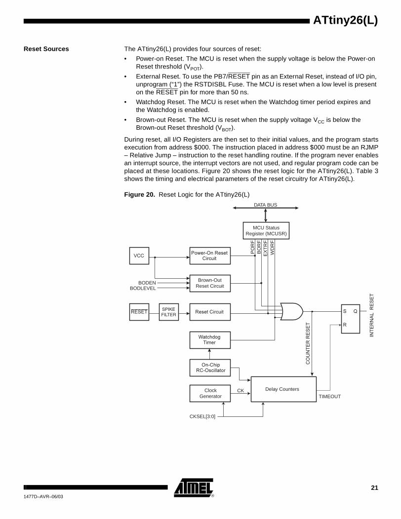
Reset Sources The ATtiny26(L) provides four sources of reset:
• Power-on Reset. The MCU is reset when the supply voltage is below the Power-on Reset threshold (VPOT).
• External Reset. To use the PB7/RESET pin as an External Reset, instead of I/O pin, unprogram (“1”) the RSTDISBL Fuse. The MCU is reset when a low level is present on the RESET pin for more than 50 ns.
• Watchdog Reset. The MCU is reset when the Watchdog timer period expires and the Watchdog is enabled.
• Brown-out Reset. The MCU is reset when the supply voltage VCC is below the Brown-out Reset threshold (VBOT).
During reset, all I/O Registers are then set to their initial values, and the program startsexecution from address $000. The instruction placed in address $000 must be an RJMP– Relative Jump – instruction to the reset handling routine. If the program never enablesan interrupt source, the interrupt vectors are not used, and regular program code can beplaced at these locations. Figure 20 shows the reset logic for the ATtiny26(L). Table 3shows the timing and electrical parameters of the reset circuitry for ATtiny26(L).
Figure 20. Reset Logic for the ATtiny26(L)
MCU StatusRegister (MCUSR)
Brown-OutReset Circuit
BODENBODLEVEL
Delay Counters
CKSEL[3:0]
CKTIMEOUT
WD
RF
BO
RF
EX
TR
F
PO
RF
DATA BUS
ClockGenerator
211477D–AVR–06/03
0
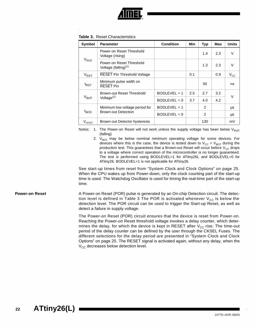
Notes: 1. The Power-on Reset will not work unless the supply voltage has been below VPOT(falling)
2. VBOT may be below nominal minimum operating voltage for some devices. Fordevices where this is the case, the device is tested down to VCC = VBOT during theproduction test. This guarantees that a Brown-out Reset will occur before VCC dropsto a voltage where correct operation of the microcontroller is no longer guaranteed.The test is performed using BODLEVEL=1 for ATtiny26L and BODLEVEL=0 forATtiny26. BODLEVEL=1 is not applicable for ATtiny26.
See start-up times from reset from “System Clock and Clock Options” on page 25.When the CPU wakes up from Power-down, only the clock counting part of the start-uptime is used. The Watchdog Oscillator is used for timing the real-time part of the start-uptime.
Power-on Reset A Power-on Reset (POR) pulse is generated by an On-chip Detection circuit. The detec-tion level is defined in Table 3 The POR is activated whenever VCC is below thedetection level. The POR circuit can be used to trigger the Start-up Reset, as well asdetect a failure in supply voltage.
The Power-on Reset (POR) circuit ensures that the device is reset from Power-on.Reaching the Power-on Reset threshold voltage invokes a delay counter, which deter-mines the delay, for which the device is kept in RESET after VCC rise. The time-outperiod of the delay counter can be defined by the user through the CKSEL Fuses. Thedifferent selections for the delay period are presented in “System Clock and ClockOptions” on page 25. The RESET signal is activated again, without any delay, when theVCC decreases below detection level.
Table 3. Reset Characteristics
Symbol Parameter Condition Min Typ Max Units
VPOT
Power-on Reset Threshold Voltage (rising)
1.4 2.3 V
Power-on Reset Threshold Voltage (falling)(1) 1.3 2.3 V
VRST RESET Pin Threshold Voltage 0.1 0.9 VCC
tRSTMinimum pulse width on RESET Pin
50 ns
VBOT
Brown-out Reset Threshold Voltage(2)
BODLEVEL = 1 2.5 2.7 3.2V
BODLEVEL = 0 3.7 4.0 4.2
tBOD
Minimum low voltage period for Brown-out Detection
BODLEVEL = 1 2 µs
BODLEVEL = 0 2 µs
VHYST Brown-out Detector hysteresis 130 mV
22 ATtiny26(L) 1477D–AVR–06/03

ATtiny26(L)
Figure 21. MCU Start-up, RESET Tied to VCC
Figure 22. MCU Start-up, RESET Controlled Externally
External Reset An External Reset is generated by a low level on the RESET pin. Reset pulses longerthan 500 ns will generate a reset, even if the clock is not running. Shorter pulses are notguaranteed to generate a reset. When the applied signal reaches the Reset ThresholdVoltage – VRST – on its positive edge, the delay timer starts the MCU after the Time-outperiod tTOUT has expired.
Figure 23. External Reset During Operation
VCC
RESET
TIME-OUT
INTERNALRESET
tTOUT
VPOT
VRST
VCC
RESET
TIME-OUT
INTERNALRESET
tTOUT
VPOT
VRST
VCC
RESET
TIME-OUT
INTERNALRESET
tTOUT
VRST
231477D–AVR–06/03
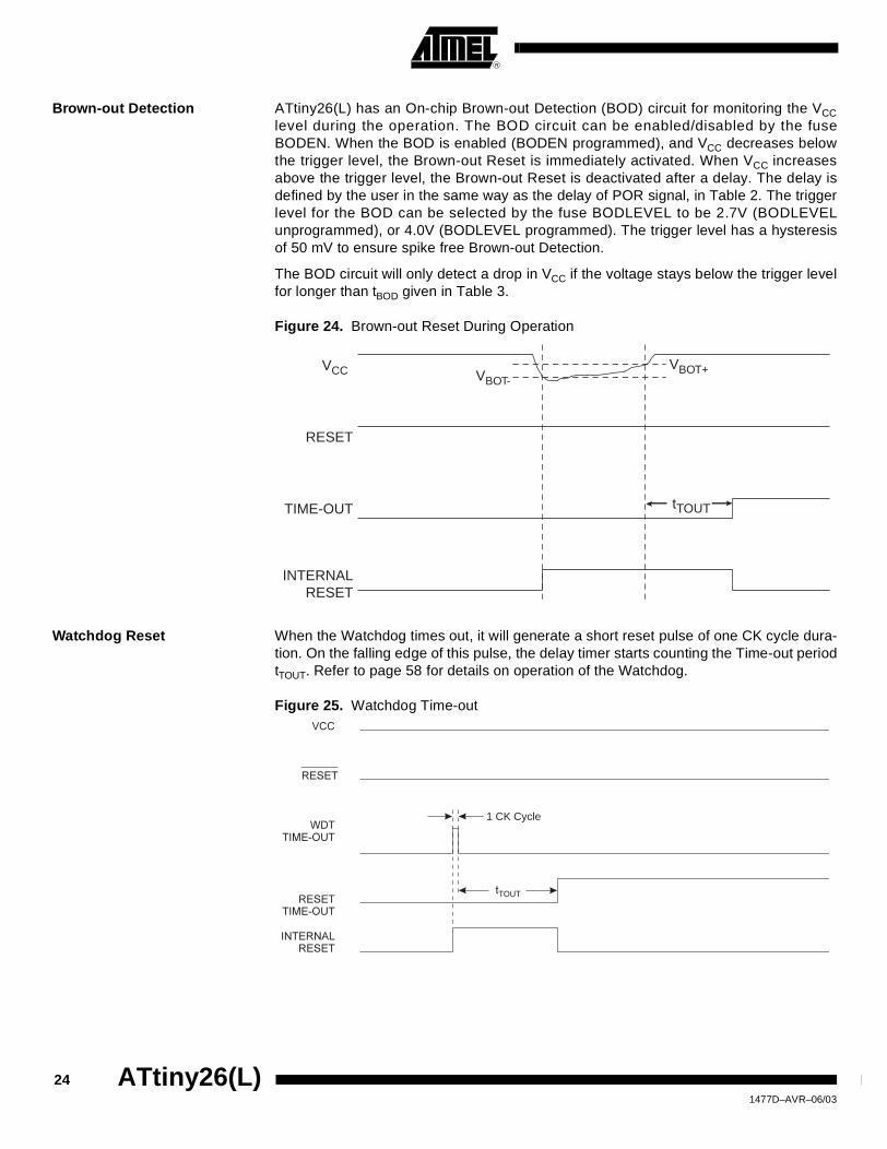
Brown-out Detection ATtiny26(L) has an On-chip Brown-out Detection (BOD) circuit for monitoring the VCClevel during the operation. The BOD circuit can be enabled/disabled by the fuseBODEN. When the BOD is enabled (BODEN programmed), and VCC decreases belowthe trigger level, the Brown-out Reset is immediately activated. When VCC increasesabove the trigger level, the Brown-out Reset is deactivated after a delay. The delay isdefined by the user in the same way as the delay of POR signal, in Table 2. The triggerlevel for the BOD can be selected by the fuse BODLEVEL to be 2.7V (BODLEVELunprogrammed), or 4.0V (BODLEVEL programmed). The trigger level has a hysteresisof 50 mV to ensure spike free Brown-out Detection.
The BOD circuit will only detect a drop in VCC if the voltage stays below the trigger levelfor longer than tBOD given in Table 3.
Figure 24. Brown-out Reset During Operation
Watchdog Reset When the Watchdog times out, it will generate a short reset pulse of one CK cycle dura-tion. On the falling edge of this pulse, the delay timer starts counting the Time-out periodtTOUT. Refer to page 58 for details on operation of the Watchdog.
Figure 25. Watchdog Time-out
VCC
RESET
TIME-OUT
INTERNALRESET
VBOT-VBOT+
tTOUT
1 CK Cycle
24 ATtiny26(L) 1477D–AVR–06/03

ATtiny26(L)
System Clock and Clock Options
Clock Systems and their Distribution
Figure 26 presents the principal clock systems in the AVR and their distribution. All ofthe clocks need not be active at a given time. In order to reduce power consumption, theclocks to modules not being used can be halted by using different sleep modes, asdescribed in “Power Management and Sleep Modes” on page 41. The clock systemsare detailed below.
Figure 26. Clock Distribution
CPU Clock – clkCPU The CPU clock is routed to parts of the system concerned with operation of the AVRcore. Examples of such modules are the General Purpose Register File, the Status Reg-ister and the data memory holding the Stack Pointer. Halting the CPU clock inhibits thecore from performing general operations and calculations.
I/O Clock – clkI/O The I/O clock is used by the majority of the I/O modules, like Timer/Counters, and USI.The I/O clock is also used by the External Interrupt module, but note that some externalinterrupts are detected by asynchronous logic, allowing such interrupts to be detectedeven if the I/O clock is halted.
Flash Clock – clkFLASH The Flash clock controls operation of the Flash interface. The Flash clock is usuallyactive simultaneously with the CPU clock.
ADC Clock – clkADC The ADC is provided with a dedicated clock domain. This allows halting the CPU andI/O clocks in order to reduce noise generated by digital circuitry. This gives more accu-rate ADC conversion results.
General I/Omodules
Timer/Counter1 ADC CPU Core RAM
clkI/O AVR ClockControl Unit
clkCPU
Flash andEEPROM
clkFLASH
clkADC
Source clock
Watchdog Timer
WatchdogOscillator
Reset Logic
ClockMultiplexer
Watchdog clock
Calibrated RCOscillator
PLLCrystal
OscillatorLow-Frequency
Crystal OscillatorExternal RC
Oscillator
clkPLL
clkPCK
External clock
251477D–AVR–06/03

Internal PLL for Fast Peripheral Clock Generation – clkPCK
The internal PLL in ATtiny26(L) generates a clock frequency that is 64x multiplied fromnominally 1 MHz input. The source of the 1 MHz PLL input clock is the output of theinternal RC Oscillator which is automatically divided down to 1 MHz, if needed. See theFigure 27 on page 26. When the PLL reference frequency is the nominal 1 MHz, the fastperipheral clock is 64 MHz. The fast peripheral clock, or a clock prescaled from that, canbe selected as the clock source for Timer/Counter1.
The PLL is locked on the RC Oscillator and adjusting the RC Oscillator via OSCCALRegister will adjust the fast peripheral clock at the same time. However, even if the pos-sibly divided RC Oscillator is taken to a higher frequency than 1 MHz, the fast peripheralclock frequency saturates at 70 MHz (worst case) and remains oscillating at the maxi-mum frequency. It should be noted that the PLL in this case is not locked any more withthe RC Oscillator clock.
Therefore it is recommended not to take the OSCCAL adjustments to a higher fre-quency than 1 MHz in order to keep the PLL in the correct operating range. The internalPLL is enabled only when the PLLE bit in the register PLLCSR is set or the PLLCK Fuseis programmed (“0”). The bit PLOCK from the register PLLCSR is set when PLL islocked.
Both internal 1 MHz RC Oscillator and PLL are switched off in Power-down and Standbysleep modes.
Figure 27. PCK Clocking System
1248 MHz
RC OSCILLATOR
OSCCAL
XTAL1
XTAL2OSCILLATORS
DIVIDETO 1 MHz
DIVIDEBY 4
CK
PLL64x
PLLCK &CKSELFUSES
PLLE
PCK
Lock Detector
PLOCK
26 ATtiny26(L) 1477D–AVR–06/03
ATtiny26(L)
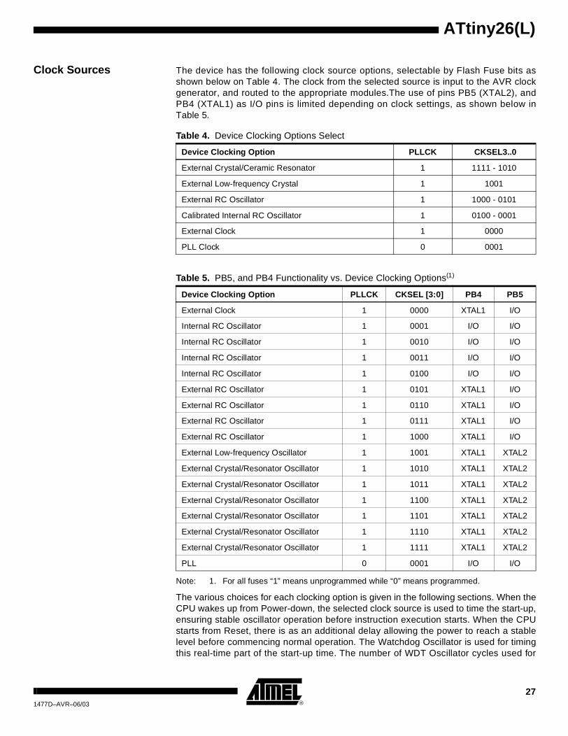
Clock Sources The device has the following clock source options, selectable by Flash Fuse bits asshown below on Table 4. The clock from the selected source is input to the AVR clockgenerator, and routed to the appropriate modules.The use of pins PB5 (XTAL2), andPB4 (XTAL1) as I/O pins is limited depending on clock settings, as shown below inTable 5.
Note: 1. For all fuses “1” means unprogrammed while “0” means programmed.
The various choices for each clocking option is given in the following sections. When theCPU wakes up from Power-down, the selected clock source is used to time the start-up,ensuring stable oscillator operation before instruction execution starts. When the CPUstarts from Reset, there is as an additional delay allowing the power to reach a stablelevel before commencing normal operation. The Watchdog Oscillator is used for timingthis real-time part of the start-up time. The number of WDT Oscillator cycles used for
Table 4. Device Clocking Options Select
Device Clocking Option PLLCK CKSEL3..0
External Crystal/Ceramic Resonator 1 1111 - 1010
External Low-frequency Crystal 1 1001
External RC Oscillator 1 1000 - 0101
Calibrated Internal RC Oscillator 1 0100 - 0001
External Clock 1 0000
PLL Clock 0 0001
Table 5. PB5, and PB4 Functionality vs. Device Clocking Options(1)
Device Clocking Option PLLCK CKSEL [3:0] PB4 PB5
External Clock 1 0000 XTAL1 I/O
Internal RC Oscillator 1 0001 I/O I/O
Internal RC Oscillator 1 0010 I/O I/O
Internal RC Oscillator 1 0011 I/O I/O
Internal RC Oscillator 1 0100 I/O I/O
External RC Oscillator 1 0101 XTAL1 I/O
External RC Oscillator 1 0110 XTAL1 I/O
External RC Oscillator 1 0111 XTAL1 I/O
External RC Oscillator 1 1000 XTAL1 I/O
External Low-frequency Oscillator 1 1001 XTAL1 XTAL2
External Crystal/Resonator Oscillator 1 1010 XTAL1 XTAL2
External Crystal/Resonator Oscillator 1 1011 XTAL1 XTAL2
External Crystal/Resonator Oscillator 1 1100 XTAL1 XTAL2
External Crystal/Resonator Oscillator 1 1101 XTAL1 XTAL2
External Crystal/Resonator Oscillator 1 1110 XTAL1 XTAL2
External Crystal/Resonator Oscillator 1 1111 XTAL1 XTAL2
PLL 0 0001 I/O I/O
271477D–AVR–06/03
each time-out is shown in Table 6. The frequency of the Watchdog Oscillator is voltagedependent as shown in the Electrical Characteristics section.
Default Clock Source The deviced is shipped with CKSEL = “0001”, SUT = “10”, and PLLCK unprogrammed.The default clock source setting is therefore the internal RC Oscillator with longest star-tup time. This default setting ensures that all users can make their desired clock sourcesetting using an In-System or Parallel Programmer.
Crystal Oscillator XTAL1 and XTAL2 are input and output, respectively, of an inverting amplifier which canbe configured for use as an On-chip Oscillator, as shown in Figure 28. Either a quartzcrystal or a ceramic resonator may be used. The maximum frequency for resonators is12 MHz. The CKOPT Fuse should always be unprogrammed when using this clockoption. C1 and C2 should always be equal. The optimal value of the capacitors dependson the crystal or resonator in use, the amount of stray capacitance, and the electromag-netic noise of the environment. Some initial guidelines for choosing capacitors for usewith crystals are given in Table 7. For ceramic resonators, the capacitor values given bythe manufacturer should be used.
Figure 28. Crystal Oscillator Connections
The Oscillator can operate in three different modes, each optimized for a specific fre-quency range. The operating mode is selected by the fuses CKSEL3..1 as shown inTable 7.
Notes: 1. The frequency ranges are preliminary values. Actual values are TBD.2. This option should not be used with crystals, only with ceramic resonators.
Table 6. Number of Watchdog Oscillator Cycles
Typ Time-out (VCC = 5.0V) Typ Time-out (VCC = 3.0V) Number of Cycles
4.1 ms 4.3 ms 4K (4,096)
65 ms 69 ms 64K (65,536)
Table 7. Crystal Oscillator Operating Modes
CKSEL3..1 Frequency
Range(1) (MHz)Recommended Range for Capacitors C1 and
C2 for Use with Crystals (pF)
101(2) 0.4 - 0.9 –
110 0.9 - 3.0 12 - 22
1113.0 - 16 12 - 22
16 - 12 - 15
XTAL2
XTAL1
GND
C2
C1
28 ATtiny26(L) 1477D–AVR–06/03

ATtiny26(L)
The CKSEL0 Fuse together with the SUT1..0 Fuses select the start-up times as shownin Table 8.
Notes: 1. These options should only be used when not operating close to the maximum fre-quency of the device, and only if frequency stability at start-up is not important for theapplication.
2. These options are intended for use with ceramic resonators and will ensure fre-quency stability at start-up. They can also be used with crystals when not operatingclose to the maximum frequency of the device, and if frequency stability at start-up isnot important for the application.
Low-frequency Crystal Oscillator
To use a 32.768 kHz watch crystal as the clock source for the device, the Low-fre-quency Crystal Oscillator must be selected by setting the PLLCK to “1” and CKSELFuses to “1001”. The crystal should be connected as shown in Figure 28. By program-ming the CKOPT Fuse, the user can enable internal capacitors on XTAL1 and XTAL2,thereby removing the need for external capacitors. The internal capacitors have a nomi-nal value of 36 pF.
When this oscillator is selected, start-up times are determined by the SUT Fuses asshown in Table 9.
Note: 1. These options should only be used if frequency stability at start-up is not importantfor the application.
Table 8. Start-up Times for the Crystal Oscillator Clock Selection
CKSEL0 SUT1..0Start-up Time
from Power-downAdditional Delay from
Reset (VCC = 5.0V)Recommended Usage
0 00 258 CK(1) 4.1 ms Ceramic resonator, fast rising power
0 01 258 CK(1) 65 ms Ceramic resonator, slowly rising power
0 10 1K CK(2) – Ceramic resonator, BOD enabled
0 11 1K CK(2) 4.1 ms Ceramic resonator, fast rising power
1 00 1K CK(2) 65 ms Ceramic resonator, slowly rising power
1 01 16K CK – Crystal Oscillator, BOD enabled
1 10 16K CK 4.1 ms Crystal Oscillator, fast rising power
1 11 16K CK 65 ms Crystal Oscillator, slowly rising power
Table 9. Start-up Times for the Low-frequency Crystal Oscillator Clock Selection
SUT1..0Start-up Time
from Power-downAdditional Delay from
Reset (VCC = 5.0V) Recommended Usage
00 1K CK(1) 4.1 ms Fast rising power or BOD enabled
01 1K CK(1) 65 ms Slowly rising power
10 32K CK 65 ms Stable frequency at start-up
11 Reserved
291477D–AVR–06/03

External RC Oscillator For timing insensitive applications, the external RC configuration shown in Figure 29can be used. The frequency is roughly estimated by the equation f = 1/(3RC). C shouldbe at least 22 pF. By programming the CKOPT Fuse, the user can enable an internal36 pF capacitor between XTAL1 and GND, thereby removing the need for an externalcapacitor.
Figure 29. External RC Configuration
The oscillator can operate in four different modes, each optimized for a specific fre-quency range. The operating mode is selected by the fuses CKSEL3..0 as shown inTable 10.
When this oscillator is selected, start-up times are determined by the SUT Fuses asshown in Table 11.
Notes: 1. This option should not be used when operating close to the maximum frequency ofthe device.
Table 10. External RC Oscillator Operating Modes
CKSEL3..0 Frequency Range (MHz)
0101 - 0.9
0110 0.9 - 3.0
0111 3.0 - 8.0
1000 8.0 - 12.0
Table 11. Start-up Times for the External RC Oscillator Clock Selection
SUT1..0Start-up Time
from Power-downAdditional Delay from
Reset (VCC = 5.0V) Recommended Usage
00 18 CK – BOD enabled
01 18 CK 4.1 ms Fast rising power
10 18 CK 65 ms Slowly rising power
11 6 CK(1) 4.1 ms Fast rising power or BOD enabled
PB5 (XTAL2)
XTAL1
GND
VCC
R
C
30 ATtiny26(L) 1477D–AVR–06/03

ATtiny26(L)
Calibrated Internal RC Oscillator
The calibrated internal RC Oscillator provides a fixed 1.0, 2.0, 4.0, or 8.0 MHz clock. Allfrequencies are nominal values at 5V and 25°C. This clock may be selected as the sys-tem clock by programming the CKSEL Fuses as shown in Table 12. If selected, it willoperate with no external components. The CKOPT Fuse should always be unpro-grammed when using this clock option. During Reset, hardware loads the calibrationbyte into the OSCCAL Register and thereby automatically calibrates the RC Oscillator.When this oscillator is used as the chip clock, the Watchdog Oscillator will still be usedfor the Watchdog Timer and for the reset time-out. For more information on the pre-pro-grammed calibration value, see the section “Calibration Byte” on page 108.
Note: 1. The device is shipped with this option selected.
When this oscillator is selected, start-up times are determined by the SUT Fuses asshown in Table 13. PB4 (XTAL1) and PB5 (XTAL2) can be used as general I/O ports.
Note: 1. The device is shipped with this option selected.
Oscillator Calibration Register – OSCCAL
• Bits 7..0 – CAL7..0: Oscillator Calibration Value
Writing the calibration byte to this address will trim the internal oscillator to remove pro-cess variations from the oscillator frequency. During Reset, the 1 MHz calibration valuewhich is located in the signature row high byte (address 0x00) is automatically loadedinto the OSCCAL Register. If the internal RC is used at other frequencies, the calibrationvalue must be loaded manually. This can be done by first reading the signature row by aprogrammer, and then store the calibration values in the Flash or EEPROM. Then thevalue can be read by software and loaded into the OSCCAl Register. When OSCCAL iszero, the lowest available frequency is chosen. Writing non-zero values to this registerwill increase the frequency of the internal oscillator. Writing $FF to the register gives thehighest available frequency. The calibrated Oscillator is used to time EEPROM andFlash access. If EEPROM or Flash is written, do not calibrate to more than 10% abovethe nominal frequency. Otherwise, the EEPROM or Flash write may fail. Note that the
Table 12. Internal Calibrated RC Oscillator Operating Modes
CKSEL3..0 Nominal Frequency (MHz)
0001(1) 1.0
0010 2.0
0011 4.0
0100 8.0
Table 13. Start-up Times for the Internal Calibrated RC Oscillator Clock Selection
SUT1..0Start-up Time from
Power-downAdditional Delay from
Reset (VCC = 5.0V) Recommended Usage
00 6 CK – BOD enabled
01 6 CK 4.1 ms Fast rising power
10(1) 6 CK 65 ms Slowly rising power
11 Reserved
Bit 7 6 5 4 3 2 1 0
$31 ($51) CAL7 CAL6 CAL5 CAL4 CAL3 CAL2 CAL1 CAL0 OSCCAL
Read/Write R/W R/W R/W R/W R/W R/W R/W R/W
Initial Value Device Specific Calibration Value
311477D–AVR–06/03
oscillator is intended for calibration to 1.0, 2.0, 4.0, or 8.0 MHz. Tuning to other values isnot guaranteed, as indicated in Table 14.
External Clock To drive the device from an external clock source, XTAL1 should be driven as shown inFigure 30. To run the device on an external clock, the CKSEL Fuses must be pro-grammed to “0000” and PLLCK to “1”. By programming the CKOPT Fuse, the user canenable an internal 36 pF capacitor between XTAL1 and GND.
Figure 30. External Clock Drive Configuration
When this clock source is selected, start-up times are determined by the SUT Fuses asshown in Table 15.
When applying an external clock, it is required to avoid sudden changes in the appliedclock frequency to ensure stable operation of the MCU. A variation in frequency of morethan 2% from one clock cycle to the next can lead to unpredictable behaviour. It isrequired to ensure that the MCU is kept in reset during such changes in the clockfrequency.
Table 14. Internal RC Oscillator Frequency Range.
OSCCAL ValueMin Frequency in Percentage of
Nominal FrequencyMax Frequency in Percentage of
Nominal Frequency
$00 50% 100%
$7F 75% 150%
$FF 100% 200%
Table 15. Start-up Times for the External Clock Selection
SUT1..0Start-up Time from
Power-downAdditional Delay from
Reset (VCC = 5.0V) Recommended Usage
00 6 CK – BOD enabled
01 6 CK 4.1 ms Fast rising power
10 6 CK 65 ms Slowly rising power
11 Reserved
EXTERNALCLOCKSIGNAL
PB5 (XTAL2)
XTAL1
GND
32 ATtiny26(L) 1477D–AVR–06/03

ATtiny26(L)
High Frequency PLL Clock – PLLCLK
There is an internal PLL that provides nominally 64 MHz clock rate locked to the RCOscillator for the use of the Peripheral Timer/Counter1 and for the system clock source.When selected as a system clock source, by programming (“0”) the fuse PLLCK, it isdivided by four. When this option is used, the CKSEL3..0 must be set to “0001”. Thisclocking option can be used only when operating between 4.5 - 5.5V to guaratee safeoperation. The system clock frequency will be 16 MHz (64 MHz/4). When using thisclock option, start-up times are determined by the SUT Fuses as shown in Table 16.See also “PCK Clocking System” on page 26.
MCU Status Register – MCUSR
• Bit 7..4 – Res: Reserved Bits
These bits are reserved bits in the ATtiny26(L) and always read as zero.
• Bit 3 – WDRF: Watchdog Reset Flag
This bit is set (one) if a Watchdog Reset occurs. The bit is reset (zero) by a Power-onReset, or by writing a logic zero to the flag.
• Bit 2 – BORF: Brown-out Reset Flag
This bit is set (one) if a Brown-out Reset occurs. The bit is reset (zero) by a Power-onReset, or by writing a logic zero to the flag.
• Bit 1 – EXTRF: External Reset Flag
This bit is set (one) if an External Reset occurs. The bit is reset (zero) by a Power-onReset, or by writing a logic zero to the flag.
• Bit 0 – PORF: Power-on Reset Flag
This bit is set (one) if a Power-on Reset occurs. The bit is reset (zero) by writing a logiczero to the flag.
To make use of the reset flags to identify a reset condition, the user should read andthen reset (zero) the MCUSR as early as possible in the program. If the register iscleared before another reset occurs, the source of the reset can be found by examiningthe reset flags.
Table 16. Start-up Times for the PLLCK
SUT1..0Start-up Time from
Power-downAdditional Delay from
Reset (VCC = 5.0V) Recommended Usage
00 1K CK – BOD enabled
01 1K CK 4.1 ms Fast rising power
10 1K CK 65 ms Slowly rising power
11 16K CK – Slowly rising power
Bit 7 6 5 4 3 2 1 0
$34 ($54) – – – – WDRF BORF EXTRF PORF MCUSR
Read/Write R R R R R/W R/W R/W R/W
Initial Value 0 0 0 0 See Bit Description
331477D–AVR–06/03

Interrupt Handling The ATtiny26(L) has two 8-bit Interrupt Mask Control Registers; GIMSK – General Inter-rupt Mask Register and TIMSK – Timer/Counter Interrupt Mask Register.
When an interrupt occurs, the Global Interrupt Enable I-bit is cleared (zero) and all inter-rupts are disabled. The user software can set (one) the I-bit to enable nested interrupts.The I-bit is set (one) when a Return from Interrupt instruction – RETI – is executed.
When the Program Counter is vectored to the actual Interrupt Vector in order to executethe interrupt handling routine, hardware clears the corresponding flag that generated theinterrupt. Some of the interrupt flags can also be cleared by writing a logic one to the flagbit position(s) to be cleared.
If an interrupt condition occurs when the corresponding interrupt enable bit is cleared(zero), the interrupt flag will be set and remembered until the interrupt is enabled, or theflag is cleared by software.
If one or more interrupt conditions occur when the Global Interrupt Enable bit is cleared(zero), the corresponding interrupt flag(s) will be set and remembered until the GlobalInterrupt Enable bit is set (one), and will be executed by order of priority.
Note that external level interrupt does not have a flag, and will only be remembered foras long as the interrupt condition is active.
Note that the Status Register is not automatically stored when entering an interrupt rou-tine and restored when returning from an interrupt routine. This must be handled bysoftware.
Interrupt Response Time The interrupt execution response for all the enabled AVR interrupts is four clock cyclesminimum. After the four clock cycles the program vector address for the actual interrupthandling routine is executed. During this four clock cycle period, the Program Counter(10 bits) is pushed onto the Stack. The vector is a relative jump to the interrupt routine,and this jump takes two clock cycles. If an interrupt occurs during execution of a multi-cycle instruction, this instruction is completed before the interrupt is served.
A return from an interrupt handling routine takes four clock cycles. During these fourclock cycles, the Program Counter (10 bits) is popped back from the Stack. When AVRexits from an interrupt, it will always return to the main program and execute one moreinstruction before any pending interrupt is served. Note that the Status Register – SREG– is not handled by the AVR hardware, neither for interrupts nor for subroutines. For theroutines requiring a storage of the SREG, this must be performed by user software.
General Interrupt Mask Register – GIMSK
• Bit 7 – Res: Reserved Bit
This bit is a reserved bit in the ATtiny26(L) and always reads as zero.
• Bit 6 – INT0: External Interrupt Request 0 Enable
When the INT0 bit is set (one) and the I-bit in the Status Register (SREG) is set (one),the external pin interrupt is enabled. The Interrupt Sense Control0 bits 1/0 (ISC01 andISC00) in the MCU general Control Register (MCUCR) define whether the externalinterrupt is activated on rising or falling edge, on pin change, or low level of the INT0 pin.Activity on the pin will cause an interrupt request even if INT0 is configured as an output.
Bit 7 6 5 4 3 2 1 0
$3B ($5B) – INT0 PCIE1 PCIE0 – – – – GIMSK
Read/Write R R/W R/W R/W R R R R
Initial Value 0 0 0 0 0 0 0 0
34 ATtiny26(L) 1477D–AVR–06/03

ATtiny26(L)
The corresponding interrupt of External Interrupt Request 0 is executed from programmemory address $001. See also “External Interrupt” on page 38.
• Bit 5 – PCIE1: Pin Change Interrupt Enable1
When the PCIE1 bit is set (one) and the I-bit in the Status Register (SREG) is set (one),the interrupt pin change is enabled on analog pins PB[7:4], PA[7:6] and PA[3]. Unlessthe alternate function masks out the interrupt, any change on the pin mentioned beforewill cause an interrupt. The corresponding interrupt of Pin Change Interrupt Request isexecuted from program memory address $002. See also “Pin Change Interrupt” onpage 38.
• Bit 4– PCIE0: Pin Change Interrupt Enable0
When the PCIE0 bit is set (one) and the I-bit in the Status Register (SREG) is set (one),the interrupt pin change is enabled on digital pins PB[3:0]. Unless the alternate functionmasks out the interrupt, any change on the pin mentioned before will cause an interrupt.The corresponding interrupt of Pin Change Interrupt Request is executed from programmemory address $002. See also “Pin Change Interrupt” on page 38.
• Bits 3..0 – Res: Reserved Bits
These bits are reserved bits in the ATtiny26(L) and always read as zero.
General Interrupt Flag Register – GIFR
• Bit 7 – Res: Reserved Bit
This bit is a reserved bit in the ATtiny26(L) and always reads as zero.
• Bit 6 – INTF0: External Interrupt Flag0
When an event on the INT0 pin triggers an interrupt request, INTF0 becomes set (one).If the I-bit in SREG and the INT0 bit in GIMSK are set (one), the MCU will jump to theInterrupt Vector at address $001. The flag is cleared when the interrupt routine is exe-cuted. Alternatively, the flag can be cleared by writing a logical one to it. The flag isalways cleared when INT0 is configured as level interrupt.
• Bit 5 – PCIF: Pin Change Interrupt Flag
When an event on pins PB[7:0], PA[7:6], or PA[3] triggers an interrupt request, PCIFbecomes set (one). PCIE1 enables interrupt from analog pins PB[7:4], PA[7:6], andPA[3]. PCIE0 enables interrupt on digital pins PB[3:0]. Note that pin change interruptenable bits PCIE1 and PCIE0 also mask the flag if they are not set. For example, ifPCIE0 is cleared, a pin change on PB[3:0] does not set PCIF. If an alternate function isenabled on a pin, PCIF is masked from that individual pin. If the I-bit in SREG and thePCIE bit in GIMSK are set (one), the MCU will jump to the Interrupt Vector at address$002. The flag is cleared when the interrupt routine is executed. Alternatively, the flagcan be cleared by writing a logical one to it. See also “Pin Change Interrupt” on page 38.
• Bits 4..0 – Res: Reserved Bits
These bits are reserved bits in the ATtiny26(L) and always read as zero.
Bit 7 6 5 4 3 2 1 0
$3A ($5A) – INTF0 PCIF – – – – – GIFR
Read/Write R R/W R/W R R R R R
Initial Value 0 0 0 0 0 0 0 0
351477D–AVR–06/03

Timer/Counter Interrupt Mask Register – TIMSK
• Bit 7 – Res: Reserved Bit
This bit is a reserved bit in the ATtiny26(L) and always reads as zero.
• Bit 6 – OCIE1A: Timer/Counter1 Output Compare Interrupt Enable
When the OCIE1A bit is set (one) and the I-bit in the Status Register is set (one), theTimer/Counter1 compare match A, interrupt is enabled. The corresponding interrupt atvector $003 is executed if a compare match A occurs. The Compare Flag inTimer/Counter1 is set (one) in the Timer/Counter Interrupt Flag Register.
• Bit 5 – OCIE1B: Timer/Counter1 Output Compare Interrupt Enable
When the OCIE1B bit is set (one) and the I-bit in the Status Register is set (one), theTimer/Counter1 compare match B, interrupt is enabled. The corresponding interrupt atvector $004 is executed if a compare match B occurs. The Compare Flag inTimer/Counter1 is set (one) in the Timer/Counter Interrupt Flag Register.
• Bit 4..3 – Res: Reserved Bits
These bits are reserved bits in the ATtiny26(L) and always read as zero.
• Bit 2 – TOIE1: Timer/Counter1 Overflow Interrupt Enable
When the TOIE1 bit is set (one) and the I-bit in the Status Register is set (one), theTimer/Counter1 Overflow interrupt is enabled. The corresponding interrupt (at vector$005) is executed if an overflow in Timer/Counter1 occurs. The Overflow Flag (Timer1)is set (one) in the Timer/Counter Interrupt Flag Register – TIFR.
• Bit 1 – TOIE0: Timer/Counter0 Overflow Interrupt Enable
When the TOIE0 bit is set (one) and the I-bit in the Status Register is set (one), theTimer/Counter0 Overflow interrupt is enabled. The corresponding interrupt (at vector$006) is executed if an overflow in Timer/Counter0 occurs. The Overflow Flag (Timer0)is set (one) in the Timer/Counter Interrupt Flag Register – TIFR.
• Bit 0 – Res: Reserved Bit
This bit is a reserved bit in the ATtiny26(L) and always reads as zero.
Bit 7 6 5 4 3 2 1 0
$39 ($59) – OCIE1A OCIE1B – – TOIE1 TOIE0 – TIMSK
Read/Write R R/W R/W R R R/W R/W R
Initial Value 0 0 0 0 0 0 0 0
36 ATtiny26(L) 1477D–AVR–06/03

ATtiny26(L)
Timer/Counter Interrupt Flag Register – TIFR
• Bit 7 – Res: Reserved Bit
This bit is a reserved bit in the ATtiny26(L) and always reads as zero.
• Bit 6 – OCF1A: Output Compare Flag 1A
The OCF1A bit is set (one) when compare match occurs between Timer/Counter1 andthe data value in OCR1A – Output Compare Register 1A. OCF1A is cleared by hard-ware when executing the corresponding interrupt handling vector. Alternatively, OCF1Ais cleared, after synchronization clock cycle, by writing a logic one to the flag. When theI-bit in SREG, OCIE1A, and OCF1A are set (one), the Timer/Counter1 A CompareMatch interrupt is executed.
• Bit 5 – OCF1B: Output Compare Flag 1B
The OCF1B bit is set (one) when compare match occurs between Timer/Counter1 andthe data value in OCR1B – Output Compare Register 1A. OCF1B is cleared by hard-ware when executing the corresponding interrupt handling vector. Alternatively, OCF1Bis cleared, after synchronization clock cycle, by writing a logic one to the flag. When theI-bit in SREG, OCIE1B, and OCF1B are set (one), the Timer/Counter1 B CompareMatch interrupt is executed.
• Bits 4..3 – Res: Reserved Bits
These bits are reserved bits in the ATtiny26(L) and always read as zero.
• Bit 2 – TOV1: Timer/Counter1 Overflow Flag
The bit TOV1 is set (one) when an overflow occurs in Timer/Counter1. TOV1 is clearedby hardware when executing the corresponding interrupt handling vector. Alternatively,TOV1 is cleared, after synchronization clock cycle, by writing a logical one to the flag.When the SREG I-bit, and TOIE1 (Timer/Counter1 Overflow Interrupt Enable), andTOV1 are set (one), the Timer/Counter1 Overflow interrupt is executed.
• Bit 1 – TOV0: Timer/Counter0 Overflow Flag
The bit TOV0 is set (one) when an overflow occurs in Timer/Counter0. TOV0 is clearedby hardware when executing the corresponding interrupt handling vector. Alternatively,TOV0 is cleared by writing a logical one to the flag. When the SREG I-bit, and TOIE0(Timer/Counter0 Overf low Interrupt Enable), and TOV0 are set (one), theTimer/Counter0 Overflow interrupt is executed.
• Bit 0 – Res: Reserved Bit
This bit is a reserved bit in the ATtiny26(L) and always reads as zero.
Bit 7 6 5 4 3 2 1 0
$38 ($58) – OCF1A OCF1B – – TOV1 TOV0 – TIFR
Read/Write R R/W R/W R R R/W R/W R
Initial Value 0 0 0 0 0 0 0 0
371477D–AVR–06/03

External Interrupt The External Interrupt is triggered by the INT0 pin. Observe that, if enabled, the interruptwill trigger even if the INT0 pin is configured as an output. This feature provides a way ofgenerating a software interrupt. The External Interrupt can be triggered by a falling orrising edge, a pin change, or a low level. This is set up as indicated in the specificationfor the MCU Control Register – MCUCR. When the External Interrupt is enabled and isconfigured as level triggered, the interrupt will trigger as long as the pin is held low.
Pin Change Interrupt The pin change interrupt is triggered by any change on any I/O pin of Port B and pinsPA3, PA6, and PA7, if the interrupt is enabled and alternate function of the pin does notmask out the interrupt. The bit PCIE1 in GIMSK enables interrupt from pins PB[7:4],PA[7:6], and PA[3]. PCIE0 enables interrupt on digital pins PB[3:0].
The pin change interrupt is different from other interrupts in two ways. First, pin changeinterrupt enable bits PCIE1 and PCIE0 also mask the flag if they are not set. The normaloperation on most interrupts is that the flag is always active and only the execution ofthe interrupt is masked by the interrupt enable.
Secondly, please note that pin change interrupt is disabled for any pin that is configuredas an alternate function. For example, no pin change interrupt is generated from pinsthat are configured as AREF, AIN0 or AIN1, OC1A, OC1A, OC1B, OC1B, XTAL1, orXTAL2 in a fuse selected clock option, Timer0 clocking, or RESET function. See Table17 for alternate functions which mask the pin change interrupt and how the function isenabled. For example pin change interrupt on the PB0 is disabled when USI Two-wiremode or USI Three-wire mode or Timer/Counter1 inverted output compare is enabled.
If the interrupt is enabled, the interrupt will trigger even if the changing pin is configuredas an output. This feature provides a way of generating a software interrupt. Alsoobserve that the pin change interrupt will trigger even if the pin activity triggers anotherinterrupt, for example the external interrupt. This implies that one external event mightcause several interrupts.
The value of the programmed fuse is “0” and unprogrammed is “1”. Each of the linesenables the alternate function so “or” function of the lines enables the function.
Table 17. Alternative Functions
Pin Alternate FunctionControl Register[Bit Name] which set the Alternate Function(1)
Bit or Fuse Value(2)
PA3 AREF ADMUX[REFS0] 1
PA6 Analog Comparator ACSR[ACD] 0
PA7 Analog Comparator ACSR[ACD] 0
PB0 USI Two-wire mode
USI Three-wire mode
TC1 compare/PWM
USICR[USIWM1]
USICR[USIWM1,USIWM0]
TCCR1A[COM1A1,COM1A0,PWM1A]
1
01
011
PB1 USI Three-wire mode
TC1 compare/PWM
USICR[USIWM1,USIWM0]
TCCR1A[COM1A1]
TCCR1A[COM1A0]
01
1
1
PB2 USI Two-wire mode
USI Three-wire mode
TC1 compare/PWM
USICR[USIWM1]
USICR[USIWM1,USIWM0]
TCCR1A[COM1B1,COM1B0,PWM1B]
1
01
011
PB3 TC1 compare/PWM TCCR1A[COM1B1]
TCCR1A[COM1B0]
1
1
38 ATtiny26(L) 1477D–AVR–06/03

ATtiny26(L)
Notes: 1. Each line represents a bit or fuse combination which enables the function.2. A fuse value of “0” is programmed, “1” is unprogrammed.
MCU Control Register – MCUCR
The MCU Control Register contains control bits for general MCU functions.
• Bits 7 – Res: Reserved Bit
This bit is a reserved bit in the ATtiny26(L) and always reads as zero.
• Bit 6 – PUD: Pull-up Disable
When this bit is set (one), the pull-ups in the I/O ports are disabled even if the DDxn andPORTxn Registers are configured to enable the pull-ups (DDxn, PORTxn = 0b01). See“Configuring the Pin” on page 91 for more details about this feature.
• Bit 5 – SE: Sleep Enable
The SE bit must be set (one) to make the MCU enter the Sleep mode when the SLEEPinstruction is executed. To avoid the MCU entering the Sleep mode unless it is the pro-grammers purpose, it is recommended to set the Sleep Enable SE bit just before theexecution of the SLEEP instruction.
• Bits 4,3 – SM1/SM0: Sleep Mode Select Bits 1 and 0
These bits select between the four available Sleep modes, as shown in the followingtable.
For details, refer to the paragraph “Sleep Modes” below.
• Bit 2 – Res: Reserved Bit
This bit is a reserved bit in the ATtiny26(L) and always reads as zero.
PB4 XTAL1, clock source FUSE[PLLCK,CKSEL]
FUSE[PLLCK,CKSEL]
10000
10101-11111
PB5 XTAL2, clock source FUSE[PLLCK,CKSEL] 11001-11111
PB6 External interrupt
TC0 clock
GIMSK[INT0],MCUCR[ISC01,ISC01]
TCCR0[CS02,CS01]
100
11
PB7 RESET RSTDISBL FUSE 1
Table 17. Alternative Functions (Continued)
Pin Alternate FunctionControl Register[Bit Name] which set the Alternate Function(1)
Bit or Fuse Value(2)
Bit 7 6 5 4 3 2 1 0
$35 ($55) – PUD SE SM1 SM0 – ISC01 ISC00 MCUCR
Read/Write R R/W R/W R/W R/W R R/W R/W
Initial Value 0 0 0 0 0 0 0 0
Table 18. Sleep Modes
SM1 SM0 Sleep Mode
0 0 Idle mode
0 1 ADC Noise Reduction mode
1 0 Power-down mode
1 1 Standby mode
391477D–AVR–06/03
• Bits 1, 0 – ISC01, ISC00: Interrupt Sense Control 0 Bit 1 and Bit 0
The External Interrupt 0 is activated by the external pin INT0 if the SREG I-flag and thecorresponding interrupt mask is set (one). The activity on the external INT0 pin that acti-vates the interrupt is defined in the following table.
Note: 1. When changing the ISC10/ISC00 bits, INT0 must be disabled by clearing its InterruptEnable bit in the GIMSK Register. Otherwise an interrupt can occur when the bits arechanged.
Table 19. Interrupt 0 Sense Control(1)
ISC01 ISC00 Description
0 0 The low level of INT0 generates an interrupt request.
0 1 Any change on INT0 generates an interrupt request.
1 0 The falling edge of INT0 generates an interrupt request.
1 1 The rising edge of INT0 generates an interrupt request.
40 ATtiny26(L) 1477D–AVR–06/03
ATtiny26(L)
Power Management and Sleep Modes
Sleep modes enable the application to shut down unused modules in the MCU, therebysaving power. The AVR provides various sleep modes allowing the user to tailor thepower consumption to the application’s requirements.
To enter any of the four sleep modes, the SE bit in MCUCR must be written to logic oneand a SLEEP instruction must be executed. The SM1, and SM0 bits in the MCUCRRegister select which sleep mode (Idle, ADC Noise Reduction, Power Down, or Stand-by) will be activated by the SLEEP instruction. See Table 18 for a summary. If anenabled interrupt occurs while the MCU is in a sleep mode, the MCU wakes up. TheMCU is then halted for four cycles in addition to the start-up time, it executes the inter-rupt routine, and resumes execution from the instruction following SLEEP. The contentsof the Register File and SRAM are unaltered when the device wakes up from sleep. If aReset occurs during sleep mode, the MCU wakes up and executes from the ResetVector.
Table 20 on page 42 presents the different clock systems in the ATtiny26, and their dis-tribution. The figure is helpful in selecting an appropriate sleep mode.
Idle Mode When the SM1..0 bits are written to “00”, the SLEEP instruction makes the MCU enterIdle mode, stopping the CPU but a l lowing Analog Comparator , ADC, USI,Timer/Counters, Watchdog, and the interrupt system to continue operating. This sleepmode basically halts clkCPU and clkFLASH, while allowing the other clocks to run.
Idle mode enables the MCU to wake up from external triggered interrupts as well asinternal ones like the Timer Overflow and USI Start and Overflow interrupts. If wake-upfrom the Analog Comparator interrupt is not required, the Analog Comparator can bepowered down by setting the ACD bit in the Analog Comparator Control and StatusRegister – ACSR. This will reduce power consumption in Idle mode. If the ADC isenabled, a conversion starts automatically when this mode is entered.
ADC Noise Reduction Mode When the SM1..0 bits are written to “01”, the SLEEP instruction makes the MCU enterADC Noise Reduction mode, stopping the CPU but allowing the ADC, the External Inter-rupts, the USI start condition detection, and the Watchdog to continue operating (ifenabled). This sleep mode basically halts clkI/O, clkCPU, and clkFLASH, while allowing theother clocks to run.
This improves the noise environment for the ADC, enabling higher resolution measure-ments. If the ADC is enabled, a conversion starts automatically when this mode isentered. Apart form the ADC Conversion Complete interrupt, only an External Reset, aWatchdog Reset, a Brown-out Reset, USI start condition interrupt, an EEPROM readyinterrupt, an External Level Interrupt on INT0, or a pin change interrupt can wake up theMCU from ADC Noise Reduction mode.
Power-down Mode When the SM1..0 bits are written to “10”, the SLEEP instruction makes the MCU enterPower-down mode. In this mode, the External Oscillator is stopped, while the ExternalInterrupts, the USI start condition detection, and the Watchdog continue operating (ifenabled). Only an External Reset, a Watchdog Reset, a Brown-out Reset, USI start con-dition interrupt, an External Level Interrupt on INT0, or a pin change interrupt can wakeup the MCU. This sleep mode basically halts all generated clocks, allowing operation ofasynchronous modules only.
When waking up from Power-down mode, there is a delay from the wake-up conditionoccurs until the wake-up becomes effective. This allows the clock to restart and becomestable after having been stopped. The wake-up period is defined by the same CKSELFuses that define the reset time-out period, as described in “Clock Sources” on page 27.
411477D–AVR–06/03

Note that if a level triggered external interrupt or pin change interrupt is used fromPower-down mode, the changed level must be held for some time to wake up the MCU.This makes the MCU less sensitive to noise. The changed level is sampled twice by theWatchdog Oscillator clock, and if both these samples have the required level, the MCUwill wake up. The period of the Watchdog Oscillator is 1.0 µs (nominal) at 3.0V and25°C. The frequency of the Watchdog Oscillator is voltage dependent as shown in theElectrical Characteristics section.
If the wake-up condition disappears before the MCU wakes up and starts to execute,e.g., a low level on INT0 is not held long enough, the interrupt causing the wake-up willnot be executed.
Standby Mode When the SM1..0 bits are “11” and an External Crystal/Resonator clock option isselected, the SLEEP instruction forces the MCU into the Standby mode. This mode isidentical to Power-down with the exception that the Oscillator is kept running. FromStandby mode, the device wakes up in only six clock cycles.
Notes: 1. Only recommended with external crystal or resonator selected as clock source.2. Only level interrupt INT0.
Table 20. Active Clock Domains and Wake-up Sources in the different Sleep Modes.
Active Clock domains Oscillators Wake-up Sources
Sleep Mode clkCPU clkFLASH clkIO clkADCMain Clock
Source EnabledINT0, and Pin
ChangeUSI Start Condition
EEPROM Ready
ADC Other I/O
Idle X X X X X X X X
ADC Noise Reduction X X X(2) X X X
Power-down X(2) X
Standby(1) X X(2) X
42 ATtiny26(L) 1477D–AVR–06/03

ATtiny26(L)
Minimizing Power Consumption
There are several issues to consider when trying to minimize the power consumption inan AVR controlled system. In general, sleep modes should be used as much as possi-ble, and the sleep mode should be selected so that as few as possible of the device’sfunctions are operating. All functions not needed should be disabled. In particular, thefollowing modules may need special consideration when trying to achieve the lowestpossible power consumption.
Analog to Digital Converter If enabled, the ADC will be enabled in all sleep modes. To save power, the ADC shouldbe disabled before entering any sleep mode. When the ADC is turned off and on again,the next conversion will be an extended conversion. Refer to “Analog to Digital Con-verter” on page 77 for details on ADC operation.
Analog Comparator When entering Idle mode, the Analog Comparator should be disabled if not used. Whenentering ADC Noise Reduction mode, the Analog Comparator should be disabled. In theother sleep modes, the Analog Comparator is automatically disabled. However, if theAnalog Comparator is set up to use the Internal Voltage Reference as input, the AnalogComparator should be disabled in all sleep modes. Otherwise, the Internal Voltage Ref-erence will be enabled, independent of sleep mode. Refer to “Analog Comparator” onpage 74 for details on how to configure the Analog Comparator.
Brown-out Detector If the Brown-out Detector is not needed in the application, this module should be turnedoff. If the Brown-out Detector is enabled by the BODEN Fuse, it will be enabled in allsleep modes, and hence, always consume power. In the deeper sleep modes, this willcontribute significantly to the total current consumption. Refer to “Brown-out Detection”on page 24 for details on how to configure the Brown-out Detector.
Internal Voltage Reference The Internal Voltage Reference will be enabled when needed by the Brown-out Detec-tor, the Analog Comparator or the ADC. If these modules are disabled as described inthe sections above, the Internal Voltage Reference will be disabled and it will not beconsuming power. When turned on again, the user must allow the reference to start upbefore the output is used. If the reference is kept on in sleep mode, the output can beused immediately.
Watchdog Timer If the Watchdog Timer is not needed in the application, this module should be turned off.If the Watchdog Timer is enabled, it will be enabled in all sleep modes, and hence,always consume power. In the deeper sleep modes, this will contribute significantly tothe total current consumption. Refer to “Watchdog Timer” on page 58 for details on howto configure the Watchdog Timer.
Port Pins When entering a sleep mode, all port pins should be configured to use minimum power.The most important thing is then to ensure that no pins drive resistive loads. In sleepmodes where the both the I/O clock (clkI/O) and the ADC clock (clkADC) are stopped, theinput buffers of the device will be disabled. This ensures that no power is consumed bythe input logic when not needed. In some cases, the input logic is needed for detectingwake-up conditions, and it will then be enabled. Refer to “Digital Input Enable and SleepModes” on page 94 for details on which pins are enabled. If the input buffer is enabledand the input signal is left floating or have an analog signal level close to VCC/2, theinput buffer will use excessive power.
431477D–AVR–06/03

Timer/Counters The ATtiny26(L) provides two general purpose 8-bi t Timer/Counters. TheTimer/Counters have separate prescaling selection from the separate prescaler. TheTimer/Counter0 clock (CK) as the clock timebase. The Timer/Counter1 has two clockingmodes, a synchronous mode and an asynchronous mode. The synchronous mode usesthe system clock (CK) as the clock timebase and asynchronous mode uses the fastperipheral clock (PCK) as the clock time base.
Timer/Counter0 Prescaler
Figure 31 below shows the Timer/Counter prescaler.
Figure 31. Timer/Counter0 Prescaler
The four prescaled selections are: CK/8, CK/64, CK/256, and CK/1024 where CK is theoscillator clock. CK, external source, and stop, can also be selected as clock sources.
10-BIT T/C PRESCALER
0
TIMER/COUNTER0 CLOCK SOURCE
CK
T0(PB6)
PSR0
CLEAR
CS00CS01CS02
CK
/8
CK
/256
CK
/102
4
CK
/64
44 ATtiny26(L) 1477D–AVR–06/03

ATtiny26(L)
Timer/Counter1 Prescaler
Figure 32 shows the Timer/Counter1 prescaler. For Timer/Counter1 the clock selectionsare between PCK to PCK/16384 and stop in asynchronous mode and CK to CK/16384and stop in synchronous. The clock options are described in Table 24 on page 52 andthe Timer/Counter1 Control Register, TCCR1B. Setting the PSR1 bit in TCCR1B Regis-ter resets the prescaler. The PCKE bit in the PLLCSR Register enables theasynchronous mode.
Figure 32. Timer/Counter1 Prescaler
8-bit Timer/Counter0 Figure 33 shows the block diagram for Timer/Counter0.
The 8-bit Timer/Counter0 can select clock source from CK, prescaled CK, or an externalpin. In addit ion, i t can be stopped as described in the specif ication for theTimer/Counter0 Control Register – TCCR0. The overflow status flag is found in theTimer/Counter Interrupt Flag Register – TIFR. Control signals are found in theTimer/Counter0 Control Register – TCCR0. The interrupt enable/disable settings forTimer/Counter0 are found in the Timer/Counter Interrupt Mask Register – TIMSK.
When Timer/Counter0 is externally clocked, the external signal is synchronized with theoscillator frequency of the CPU. To ensure proper sampling of the external clock, theminimum time between two external clock transitions must be at least one internal CPUclock period. The external clock signal is sampled on the rising edge of the internal CPUclock.
The 8-bit Timer/Counter0 features both a high resolution and a high accuracy usagewith the lower prescaling opportunities. Similarly, the high prescaling opportunities makethe Timer/Counter0 useful for lower speed functions or exact timing functions with infre-quent actions.
TIMER/COUNTER1 COUNT ENABLE
PSR1
CS10CS11CS12
PCK(64 MHz)
0
CS13
14-BITT/C PRESCALER
T1C
K/2
T1C
K
T1C
K/4
T1C
K/8
T1C
K/1
6
T1C
K/3
2
T1C
K/6
4
T1C
K/1
28
T1C
K/2
56
T1C
K/5
12
T1C
K/1
024
T1C
K/2
048
T1C
K/4
096
T1C
K/8
192
T1C
K/1
6384
SA
CK
PCKE
T1CK
451477D–AVR–06/03
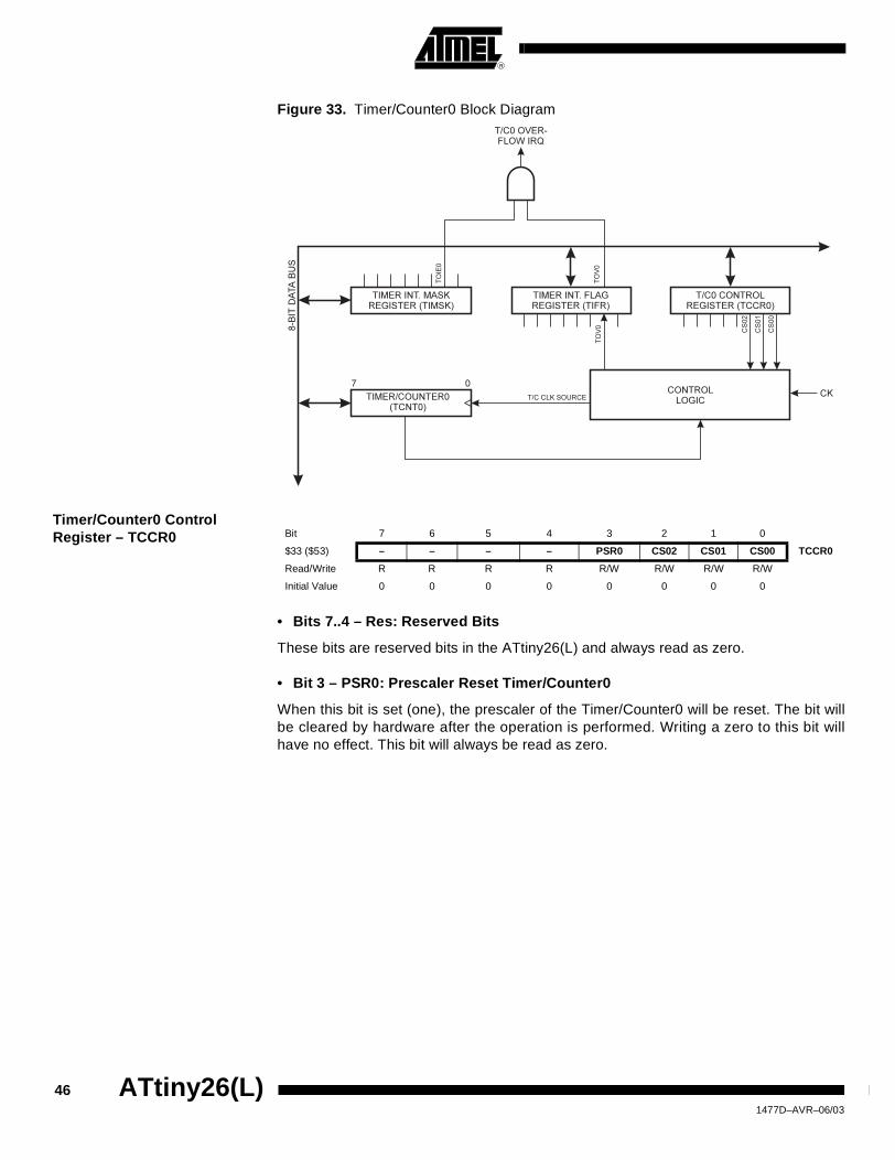
Figure 33. Timer/Counter0 Block Diagram
Timer/Counter0 Control Register – TCCR0
• Bits 7..4 – Res: Reserved Bits
These bits are reserved bits in the ATtiny26(L) and always read as zero.
• Bit 3 – PSR0: Prescaler Reset Timer/Counter0
When this bit is set (one), the prescaler of the Timer/Counter0 will be reset. The bit willbe cleared by hardware after the operation is performed. Writing a zero to this bit willhave no effect. This bit will always be read as zero.
Bit 7 6 5 4 3 2 1 0
$33 ($53) – – – – PSR0 CS02 CS01 CS00 TCCR0
Read/Write R R R R R/W R/W R/W R/W
Initial Value 0 0 0 0 0 0 0 0
46 ATtiny26(L) 1477D–AVR–06/03

ATtiny26(L)
• Bits 2, 1, 0 – CS02, CS01, CS00: Clock Select0, Bit 2, 1, and 0
The Clock Select0 bits 2, 1, and 0 define the prescaling source of Timer0.
The Stop condition provides a Timer Enable/Disable function. The CK down dividedmodes are scaled directly from the CK oscillator clock. If the external pin modes areused, the corresponding setup must be performed in the actual Data Direction ControlRegister (cleared to zero gives an input pin).
Timer/Counter0 – TCNT0
The Timer/Counter0 is implemented as an up-counter with read and write access. If theTimer/Counter0 is written and a clock source is present, the Timer/Counter0 continuescounting in the timer clock cycle following the write operation.
8-bit Timer/Counter1 The Timer/Counter1 has two clocking modes: a synchronous mode and an asynchro-nous mode. The synchronous mode uses the system clock (CK) as the clock timebaseand asynchronous mode uses the fast peripheral clock (PCK) as the clock time base.The PCKE bit from the PLLCSR Register enables the asynchronous mode when it is set(“1”). The Timer/Counter1 general operation is described in the asynchronous mode andthe operation in the synchronous mode is mentioned only if there is differences betweenthese two modes. Figure 34 shows Timer/Counter1 synchronization register block dia-gram and synchronization delays in between registers. Note that all clock gating detailsare not shown in the figure. The Timer/Counter1 Register values go through the internalsynchronization registers, which cause the input synchronization delay, before affectingthe counter operation. The registers TCCR1A, TCCR1B, OCR1A, OCR1B, and OCR1Ccan be read back right after writing the register. The read back values are delayed forthe Timer/Counter1 (TCNT1) Register and flags (OCF1A, OCF1B, and TOV1), becauseof the input and output synchronization.
This module features a high resolution and a high accuracy usage with the lower pres-caling opportunities. Timer/Counter1 can also support two accurate, high speed, 8-bitPulse Width Modulators using clock speeds up to 64 MHz. In this mode, Timer/Counter1and the Output Compare Registers serve as dual stand-alone PWMs with non-overlap-ping non-inverted and inverted outputs. Refer to page 54 for a detailed description onthis function. Similarly, the high prescaling opportunities make this unit useful for lowerspeed functions or exact timing functions with infrequent actions.
Table 21. Clock 0 Prescale Select
CS02 CS01 CS00 Description
0 0 0 Stop, the Timer/Counter0 is stopped
0 0 1 CK
0 1 0 CK/8
0 1 1 CK/64
1 0 0 CK/256
1 0 1 CK/1024
1 1 0 External Pin T0, falling edge
1 1 1 External Pin T0, rising edge
Bit 7 6 5 4 3 2 1 0
$32 ($52) MSB LSB TCNT0
Read/Write R/W R/W R/W R/W R/W R/W R/W R/W
Initial Value 0 0 0 0 0 0 0 0
471477D–AVR–06/03

Figure 34. Timer/Counter1 Synchronization Register Block Diagram
Timer/Counter1 and the prescaler allow running the CPU from any clock source whilethe prescaler is operating on the fast 64 MHz PCK clock in the asynchronous mode.
Note that the system clock frequency must be lower than one half of the PCK frequency.Only when the system clock is generated from PCK dividing that by two, the ratio of thePCK/system clock can be exactly two. The synchronization mechanism of the asynchro-nous Timer/Counter1 needs at least two edges of the PCK when the system clock ishigh. If the frequency of the system clock is too high, it is a risk that data or control val-ues are lost.
The following Figure 35 shows the block diagram for Timer/Counter1.
OCR1A
8-BIT DATABUS
SYNCMODE
1CK delay
TCNT1
CK
OCF1A
OCF1B
TCNT1
TOV1
OCR1B
OCR1C
TCCR1A
TCCR1B
OCR1A_SI
OCR1B_SI
OCR1C_SI
TCCR1A_SI
TCCR1B_SI
TCNT1
OCF1A
OCF1B
TOV1
TCNT1_SI
OCF1A_SI
OCF1B_SI
TOV1_SI
TCNT_SO
OCF1A_SO
OCF1B_SO
TOV1_SO
SA
ASYNCMODE
1PCK delay 1/2PCK -1CK delay 1/2PCK -1CK delay
PCK
PCKE
SA
SA
SA
SA
SA
no delay
no delay
IO-registers Input syncronizationregisters
Timer/Counter1 Outputmultiplexers
Outputsyncronizationregisters
48 ATtiny26(L) 1477D–AVR–06/03

ATtiny26(L)
Figure 35. Timer/Counter1 Block Diagram
Three status flags (overflow and compare matches) are found in the Timer/CounterInterrupt Flag Register – TIFR. Control signals are found in the Timer/Counter ControlRegisters TCCR1A and TCCR1B. The interrupt enable/disable settings are found in theTimer/Counter Interrupt Mask Register – TIMSK.
The Timer/Counter1 contains three Output Compare Registers, OCR1A, OCR1B, andOCR1C, as the data source to be compared with the Timer/Counter1 contents. In nor-mal mode the Output Compare functions are operational with all three Output CompareRegisters. OCR1A determines action on the OC1A pin (PB1), and it can generateTimer1 OC1A interrupt in normal mode and in PWM mode. Likewise, OCR1B deter-mines action on the OC1B pin (PB3) and it can generate Timer1 OC1B interrupt innormal mode and in PWM mode. OCR1C holds the Timer/Counter maximum value, i.e.,the clear on compare match value. An overflow interrupt (TOV1) is generated whenTimer/Counter1 counts from $FF to $00 or from OCR1C to $00. This function is thesame for both normal and PWM mode. The inverted PWM outputs OC1A and OC1B arenot connected in normal mode.
In PWM mode, OCR1A and OCR1B provide the data values against which theTimer/Counter value is compared. Upon compare match the PWM outputs (OC1A,OC1A, OC1B, OC1B) are generated. In PWM mode, the Timer/Counter counts up to thevalue specified in the Output Compare Register OCR1C and starts again from $00. Thisfeature allows limiting the counter “full” value to a specified value, lower than $FF.Together with the many prescaler options, flexible PWM frequency selection is provided.Table 27 lists clock selection and OCR1C values to obtain PWM frequencies from 20kHz to 250 kHz in 10 kHz steps and from 250 kHz to 500 kHz in 50 kHz steps. HigherPWM frequencies can be obtained at the expense of resolution.
8-BIT DATA BUS
TIMER INT. FLAGREGISTER (TIFR)
TIMER/COUNTER1
8-BIT COMPARATOR
T/C1 OUTPUTCOMPARE REGISTER
TIMER INT. MASKREGISTER (TIMSK)
TIMER/COUNTER1(TCNT1)
T/C CLEAR T/C1 CONTROLLOGIC
TO
V1
OC
F1B
OC
F1B
TO
V1
TO
IE0
TO
IE1
OC
IE1B
OC
IE1A
OC
F1A
OC
F1A
CK
PCK
T/C1 OVER-FLOW IRQ
T/C1 COMPAREMATCH B IRQ
OC1A(PB1)
T/C1 COMPAREMATCH A IRQ
T/C CONTROLREGISTER 1 (TCCR1A)
CO
M1B
1
PW
M1A
PW
M1B
CO
M1B
0
FO
C1A
FO
C1B
(OCR1A) (OCR1B) (OCR1C)
8-BIT COMPARATOR
T/C1 OUTPUTCOMPARE REGISTER
TO
V0
CO
M1A
1
CO
M1A
0
T/C CONTROLREGISTER 1 (TCCR1A)
OC1A(PB0)
OC1B(PB3)
OC1B(PB2)
8-BIT COMPARATOR
T/C1 OUTPUTCOMPARE REGISTER
T/C CONTROLREGISTER 1 (TCCR1B)
CS
12
PS
R1
CS
11
CS
10
CS
13
CT
C1
491477D–AVR–06/03

Timer/Counter1 Control Register A – TCCR1A
• Bits 7, 6 – COM1A1, COM1A0: Comparator A Output Mode, Bits 1 and 0
The COM1A1 and COM1A0 control bits determine any output pin action following aCompare Match with Compare Register A in Timer/Counter1. Output pin actions affectpin PB1 (OC1A). Since this is an alternative function to an I/O port, the correspondingdirection control bit must be set (one) in order to control an output pin. Note that OC1A isnot connected in normal mode.
In PWM mode, these bits have different functions. Refer to Table 25 on page 55 for adetailed description.
• Bits 5, 4 – COM1B1, COM1B0: Comparator B Output Mode, Bits 1 and 0
The COM1B1 and COM1B0 control bits determine any output pin action following aCompare Match with Compare Register B in Timer/Counter1. Output pin actions affectpin PB3 (OC1B). Since this is an alternative function to an I/O port, the correspondingdirection control bit must be set (one) in order to control an output pin. Note that OC1B isnot connected in normal mode.
In PWM mode, these bits have different functions. Refer to Table 25 on page 55 for adetailed description.
• Bit 3 – FOC1A: Force Output Compare Match 1A
Writing a logical one to this bit forces a change in the Compare Match output pin PB1(OC1A) according to the values already set in COM1A1 and COM1A0. If COM1A1 andCOM1A0 written in the same cycle as FOC1A, the new settings will be used. The ForceOutput Compare bit can be used to change the output pin value regardless of the timervalue. The automatic action programmed in COM1A1 and COM1A0 takes place as if acompare match had occurred, but no interrupt is generated. The FOC1A bit alwaysreads as zero. FOC1A is not in use if PWM1A bit is set.
Bit 7 6 5 4 3 2 1 0
$30 ($50) COM1A1 COM1A0 COM1B1 COM1B0 FOC1A FOC1B PWM1A PWM1B TCCR1A
Read/Write R/W R/W R/W R/W R/W R/W R/W R/W
Initial Value 0 0 0 0 0 0 0 0
Table 22. Comparator A Mode Select
COM1A1 COM1A0 Description
0 0 Timer/Counter Comparator A disconnected from output pin OC1A.
0 1 Toggle the OC1A output line.
1 0 Clear the OC1A output line.
1 1 Set the OC1A output line.
Table 23. Comparator B Mode Select
COM1B1 COM1B0 Description
0 0 Timer/Counter Comparator B disconnected from output pin OC1B.
0 1 Toggle the OC1B output line.
1 0 Clear the OC1B output line.
1 1 Set the OC1B output line.
50 ATtiny26(L) 1477D–AVR–06/03

ATtiny26(L)
• Bit 2 – FOC1B: Force Output Compare Match 1B
Writing a logical one to this bit forces a change in the Compare Match output pin PB3(OC1B) according to the values already set in COM1B1 and COM1B0. If COM1B1 andCOM1B0 written in the same cycle as FOC1B, the new settings will be used. The ForceOutput Compare bit can be used to change the output pin value regardless of the timervalue. The automatic action programmed in COM1B1 and COM1B0 takes place as if acompare match had occurred, but no interrupt is generated. The FOC1B bit alwaysreads as zero. FOC1B is not in use if PWM1B bit is set.
• Bit 1 – PWM1A: Pulse Width Modulator A Enable
When set (one) this bit enables PWM mode based on comparator OCR1A inTimer/Counter1 and the counter value is reset to $00 in the CPU clock cycle after acompare match with OCR1C Register value.
• Bit 0 – PWM1B: Pulse Width Modulator B Enable
When set (one) this bit enables PWM mode based on comparator OCR1B inTimer/Counter1 and the counter value is reset to $00 in the CPU clock cycle after acompare match with OCR1C Register value.
Timer/Counter1 Control Register B – TCCR1B
• Bit 7 – CTC1: Clear Timer/Counter on Compare Match
When the CTC1 control bit is set (one), Timer/Counter1 is reset to $00 in the CPU clockcycle after a compare match with OCR1C Register value. If the control bit is cleared,Timer/Counter1 continues counting and is unaffected by a compare match.
• Bit 6 – PSR1: Prescaler Reset Timer/Counter1
When this bit is set (one), the Timer/Counter prescaler will be reset. The bit will becleared by hardware after the operation is performed. Writing a zero to this bit will haveno effect. This bit will always read as zero.
• Bit 5..4 – Res: Reserved Bits
These bits are reserved bits in the ATtiny26(L) and always read as zero.
Bit 7 6 5 4 3 2 1 0
$2F ($4F) CTC1 PSR1 – – CS13 CS12 CS11 CS10 TCCR1B
Read/Write R/W R/W R R R/W R/W R/W R/W
Initial Value 0 0 0 0 0 0 0 0
511477D–AVR–06/03

• Bits 3..0 – CS13, CS12, CS11, CS10: Clock Select Bits 3, 2, 1, and 0
The Clock Select bits 3, 2, 1, and 0 define the prescaling source of Timer/Counter1.
The Stop condition provides a Timer Enable/Disable function.
Timer/Counter1 – TCNT1
This 8-bit register contains the value of Timer/Counter1.
Timer/Counter1 is realized as an up counter with read and write access. Due to syn-chronization of the CPU, Timer/Counter1 data written into Timer/Counter1 is delayed byone CPU clock cycle in synchronous mode and at most two CPU clock cycles for asyn-chronous mode.
Timer/Counter1 Output Compare RegisterA – OCR1A
The Output Compare Register A is an 8-bit read/write register.
The Timer/Counter Output Compare Register A contains data to be continuously com-pared with Timer/Counter1. Actions on compare matches are specified in TCCR1A. Acompare match does only occur if Timer/Counter1 counts to the OCR1A value. A soft-
Table 24. Timer/Counter1 Prescale Select
CS13 CS12 CS11 CS10DescriptionAsynchronous Mode
DescriptionSynchronous Mode
0 0 0 0 Timer/Counter1 is stopped. Timer/Counter1 is stopped.
0 0 0 1 PCK CK
0 0 1 0 PCK/2 CK/2
0 0 1 1 PCK/4 CK/4
0 1 0 0 PCK/8 CK/8
0 1 0 1 PCK/16 CK/16
0 1 1 0 PCK/32 CK/32
0 1 1 1 PCK/64 CK/64
1 0 0 0 PCK/128 CK/128
1 0 0 1 PCK/256 CK/256
1 0 1 0 PCK/512 CK/512
1 0 1 1 PCK/1024 CK/1024
1 1 0 0 PCK/2048 CK/2048
1 1 0 1 PCK/4096 CK/4096
1 1 1 0 PCK/8192 CK/8192
1 1 1 1 PCK/16384 CK/16384
Bit 7 6 5 4 3 2 1 0
$2E ($4E) MSB LSB TCNT1
Read/Write R/W R/W R/W R/W R/W R/W R/W R/W
Initial Value 0 0 0 0 0 0 0 0
Bit 7 6 5 4 3 2 1 0
$2D ($4D) MSB LSB OCR1A
Read/Write R/W R/W R/W R/W R/W R/W R/W R/W
Initial Value 0 0 0 0 0 0 0 0
52 ATtiny26(L) 1477D–AVR–06/03

ATtiny26(L)
ware write that sets TCNT1 and OCR1A to the same value does not generate acompare match.
A compare match will set the compare interrupt flag OCF1A after a synchronizationdelay following the compare event.
Timer/Counter1 Output Compare RegisterB – OCR1B
The Output Compare Register B is an 8-bit read/write register.
The Timer/Counter Output Compare Register B contains data to be continuously com-pared with Timer/Counter1. Actions on compare matches are specified in TCCR1A. Acompare match does only occur if Timer/Counter1 counts to the OCR1B value. A soft-ware write that sets TCNT1 and OCR1B to the same value does not generate acompare match.
A compare match will set the compare interrupt flag OCF1B after a synchronizationdelay following the compare event.
Timer/Counter1 Output Compare RegisterC – OCR1C
The Output Compare Register C is an 8-bit read/write register.
The Timer/Counter Output Compare Register C contains data to be continuously com-pared with Timer/Counter1. A compare match does only occur if Timer/Counter1 countsto the OCR1C value. A software write that sets TCNT1 and OCR1C to the same valuedoes not generate a compare match.
If the CTC1 bit in TCCR1B is set, a compare match will clear TCNT1 and set an Over-flow Interrupt Flag (TOV1). The flag is set after a synchronization delay following thecompare event.
This register has the same function in normal mode and PWM mode.
PLL Control and Status Register – PLLCSR
• Bit 7..3 – Res: Reserved Bits
These bits are reserved bits in the ATtiny26(L) and always read as zero.
• Bit 2 – PCKE: PCK Enable
The PCKE bit change the Timer/Counter1 clock source. When it is set, the asynchro-nous clock mode is enabled and fast 64 MHz PCK clock is used as Timer/Counter1clock source. If this bit is cleared, the synchronous clock mode is enabled, and systemclock CK is used as Timer/Counter1 clock source. This bit can be set only if PLLE bit isset. It is safe to set this bit only when the PLL is locked i.e., the PLOCK bit is 1.
Bit 7 6 5 4 3 2 1 0
$2C ($4C) MSB LSB OCR1B
Read/Write R/W R/W R/W R/W R/W R/W R/W R/W
Initial Value 0 0 0 0 0 0 0 0
Bit 7 6 5 4 3 2 1 0
$2B ($4B) MSB LSB OCR1C
Read/Write R/W R/W R/W R/W R/W R/W R/W R/W
Initial Value 0 0 0 0 0 0 0 0
Bit 7 6 5 4 3 2 1 0
$29 ($29) – – – – – PCKE PLLE PLOCK PLLCSR
Read/Write R R R R R R/W R/W R
Initial Value 0 0 0 0 0 0 0/1 0
531477D–AVR–06/03
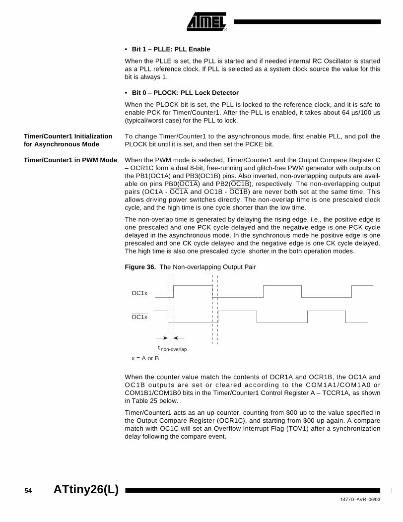
• Bit 1 – PLLE: PLL Enable
When the PLLE is set, the PLL is started and if needed internal RC Oscillator is startedas a PLL reference clock. If PLL is selected as a system clock source the value for thisbit is always 1.
• Bit 0 – PLOCK: PLL Lock Detector
When the PLOCK bit is set, the PLL is locked to the reference clock, and it is safe toenable PCK for Timer/Counter1. After the PLL is enabled, it takes about 64 µs/100 µs(typical/worst case) for the PLL to lock.
Timer/Counter1 Initialization for Asynchronous Mode
To change Timer/Counter1 to the asynchronous mode, first enable PLL, and poll thePLOCK bit until it is set, and then set the PCKE bit.
Timer/Counter1 in PWM Mode When the PWM mode is selected, Timer/Counter1 and the Output Compare Register C– OCR1C form a dual 8-bit, free-running and glitch-free PWM generator with outputs onthe PB1(OC1A) and PB3(OC1B) pins. Also inverted, non-overlapping outputs are avail-able on pins PB0(OC1A) and PB2(OC1B), respectively. The non-overlapping outputpairs (OC1A - OC1A and OC1B - OC1B) are never both set at the same time. Thisallows driving power switches directly. The non-overlap time is one prescaled clockcycle, and the high time is one cycle shorter than the low time.
The non-overlap time is generated by delaying the rising edge, i.e., the positive edge isone prescaled and one PCK cycle delayed and the negative edge is one PCK cycledelayed in the asynchronous mode. In the synchronous mode he positive edge is oneprescaled and one CK cycle delayed and the negative edge is one CK cycle delayed.The high time is also one prescaled cycle shorter in the both operation modes.
Figure 36. The Non-overlapping Output Pair
When the counter value match the contents of OCR1A and OCR1B, the OC1A andOC1B ou tpu ts a re set o r c leared according to the COM1A1/COM1A0 o rCOM1B1/COM1B0 bits in the Timer/Counter1 Control Register A – TCCR1A, as shownin Table 25 below.
Timer/Counter1 acts as an up-counter, counting from $00 up to the value specified inthe Output Compare Register (OCR1C), and starting from $00 up again. A comparematch with OC1C will set an Overflow Interrupt Flag (TOV1) after a synchronizationdelay following the compare event.
OC1x
OC1x
x = A or B
t non-overlap
54 ATtiny26(L) 1477D–AVR–06/03

ATtiny26(L)
Note that in PWM mode, writing to the Output Compare Registers OCR1A or OCR1B,the data value is first transferred to a temporary location. The value is latched intoOCR1A or OCR1B when the Timer/Counter reaches OCR1C. This prevents the occur-rence of odd-length PWM pulses (glitches) in the event of an unsynchronized OCR1A orOCR1B. See Figure 37 for an example.
Figure 37. Effects of Unsynchronized OCR Latching
During the time between the write and the latch operation, a read from OCR1A orOCR1B will read the contents of the temporary location. This means that the mostrecently written value always will read out of OCR1A or OCR1B.
When OCR1A or OCR1B contain $00 or the top value, as specified in OCR1C Register,the output PB1(OC1A) or PB3(OC1B) is held low or high according to the settings ofCOM1A1/COM1A0. This is shown in Table 26.
Table 25. Compare Mode Select in PWM Mode
COM1x1 COM1x0 Effect on Output Compare Pins
0 0OC1x not connected.
OC1x not connected.
0 1
OC1x cleared on compare match. Set one prescaled cycle after TCNT1 = $01.
OC1x set one prescaled cycle after compare match. Cleared when TCNT1 = $00.
1 0OC1x cleared on compare match. Set when TCNT1 = $01.
OC1x not connected.
1 1OC1x set one prescaled cycle after compare match. Cleared when TCNT = $00
OC1x not connected.
PWM Output OC1x
PWM Output OC1xUnsynchronized OC1x Latch
Synchronized OC1x Latch
Counter Value
Compare Value
Counter Value
Compare Value
Compare Value changes
Glitch
Compare Value Changes
551477D–AVR–06/03
In PWM mode, the Timer Overflow Flag – TOV1, is set as in normal Timer/Countermode. Timer Overflow Interrupt1 operates exactly as in normal Timer/Counter mode,i.e., it is executed when TOV1 is set provided that Timer Overflow Interrupt and globalinterrupts are enabled. This also applies to the Timer Output Compare flags andinterrupts.
The frequency of the PWM will be Timer Clock 1 Frequency divided by (OCR1Cvalue + 1). See the following equation:
Resolution shows how many bit is required to express the value in the OCR1C Register.It is calculated by following equation
ResolutionPWM = log2(OCR1C + 1)
Table 26. PWM Outputs OCR1x = $00 or OCR1C, x = A or B
COM1x1 COM1x0 OCR1x Output OC1x Output OC1x
0 1 $00 L H
0 1 OCR1C H L
1 0 $00 L Not connected
1 0 OCR1C H Not connected
1 1 $00 H Not connected
1 1 OCR1C L Not connected
fPWMfTCK1
OCR1C + 1( )------------------------------------=
56 ATtiny26(L) 1477D–AVR–06/03

ATtiny26(L)
Table 27. Timer/Counter1 Clock Prescale Select in the Asynchronous Mode
PWM Frequency (kHz) Clock Selection CS13..CS10 OCR1C RESOLUTION (Bits)
20 PCK/16 0101 199 7.6
30 PCK/16 0101 132 7.1
40 PCK/8 0100 199 7.6
50 PCK/8 0100 159 7.3
60 PCK/8 0100 132 7.1
70 PCK/4 0011 228 7.8
80 PCK/4 0011 199 7.6
90 PCK/4 0011 177 7.5
100 PCK/4 0011 159 7.3
110 PCK/4 0011 144 7.2
120 PCK/4 0011 132 7.1
130 PCK/2 0010 245 7.9
140 PCK/2 0010 228 7.8
150 PCK/2 0010 212 7.7
160 PCK/2 0010 199 7.6
170 PCK/2 0010 187 7.6
180 PCK/2 0010 177 7.5
190 PCK/2 0010 167 7.4
200 PCK/2 0010 159 7.3
250 PCK 0001 255 8.0
300 PCK 0001 212 7.7
350 PCK 0001 182 7.5
400 PCK 0001 159 7.3
450 PCK 0001 141 7.1
500 PCK 0001 127 7.0
571477D–AVR–06/03

Watchdog Timer The Watchdog Timer is clocked from a separate On-chip Oscillator which runs at 1MHz. This is the typical value at VCC = 5V. See characterization data for typical values atother VCC levels. By controlling the Watchdog Timer prescaler, the Watchdog Resetinterval can be adjusted from 16 to 2048 ms. The WDR – Watchdog Reset – instructionresets the Watchdog Timer. Eight different clock cycle periods can be selected to deter-mine the reset period. If the reset period expires without another Watchdog Reset, theATtiny26(L) resets and executes from the Reset Vector. For timing details on the Watch-dog Reset, refer to page 24.
To prevent unintentional disabling of the Watchdog, a special turn-off sequence must befollowed when the Watchdog is disabled. Refer to the description of the Watchdog TimerControl Register for details.
Figure 38. Watchdog Timer
Watchdog Timer Control Register – WDTCR
• Bits 7..5 – Res: Reserved Bits
These bits are reserved bits in the ATtiny26(L) and will always read as zero.
• Bit 4 – WDCE: Watchdog Change Enable
This bit must be set when the WDE bit is written to logic zero. Otherwise, the Watchdogwill not be disabled. Once written to one, hardware will clear this bit after four clockcycles. Refer to the description of the WDE bit for a Watchdog disable procedure. InSafety Level 1 and 2, this bit must also be set when changing the prescaler bits.
• Bit 3 – WDE: Watchdog Enable
When the WDE is set (one) the Watchdog Timer is enabled, and if the WDE is cleared(zero) the Watchdog Timer function is disabled. WDE can be cleared only when theWDCE bit is set(one). To disable an enabled Watchdog Timer, the following proceduremust be followed:
Normally 1 MHzWATCHDOG
PRESCLALER
WATCHDOGRESET
WDP0WDP1WDP2
WDE
MCU RESET
Bit 7 6 5 4 3 2 1 0
$21 ($41) – – – WDCE WDE WDP2 WDP1 WDP0 WDTCR
Read/Write R R R R/W R/W R/W R/W R/W
Initial Value 0 0 0 0 0 0 0 0
58 ATtiny26(L) 1477D–AVR–06/03
ATtiny26(L)
1. In the same operation, write a logical one to WDCE and WDE. A logical one must be written to WDE even though it is set to one before the disable operation starts.
2. Within the next four clock cycles, write a logical 0 to WDE. This disables the Watchdog.
• Bits 2..0 – WDP2, WDP1, WDP0: Watchdog Timer Prescaler 2, 1, and 0
The WDP2, WDP1 and WDP0 bits determine the Watchdog Timer prescaling when theWatchdog Timer is enabled. The different prescaling values and their correspondingtime-out periods are shown in Table 28.
Note: 1. The frequency of the Watchdog Oscillator is voltage dependent. The WDR – Watch-dog Reset – instruction should always be executed before the Watchdog Timer isenabled. This ensures that the reset period will be in accordance with the WatchdogTimer prescale settings. If the Watchdog Timer is enabled without reset, the Watch-dog Timer may not start counting from zero.
Table 28. Watchdog Timer Prescale Select(1)
WDP2 WDP1 WDP0Number of WDT Oscillator Cycles
Typical Time-out at VCC = 3.0V
Typical Time-out at VCC = 5.0V
0 0 0 16K (16,384) 17.1 ms 16.3 ms
0 0 1 32K (32,768) 34.3 ms 32.5 ms
0 1 0 64K (65,536) 68.5 ms 65 ms
0 1 1 128K (131,072) 0.14 s 0.13 s
1 0 0 256K (262,144) 0.27 s 0.26 s
1 0 1 512K (524,288) 0.55 s 0.52 s
1 1 0 1,024K (1,048,576) 1.1 s 1.0 s
1 1 1 2,048K (2,097,152) 2.2 s 2.1 s
591477D–AVR–06/03

EEPROM Read/Write Access
The EEPROM Access Registers are accessible in the I/O space.
The write access time is typically 8.3 ms. A self-timing function lets the user softwaredetect when the next byte can be written. A special EEPROM Ready Interrupt can beset to trigger when the EEPROM is ready to accept new data.
An ongoing EEPROM write operation will complete even if a reset condition occurs.
In order to prevent unintentional EEPROM writes, a two state write procedure must befollowed. Refer to the description of the EEPROM Control Register for details on this.
When the EEPROM is written, the CPU is halted for two clock cycles before the nextinstruction is executed.
When the EEPROM is read, the CPU is halted for four clock cycles before the nextinstruction is executed.
EEPROM Address Register – EEAR
• Bit 7 – RES: Reserved Bits
This bit are reserved bit in the ATtiny26(L) and will always read as zero.
• Bit 6..0 – EEAR6..0: EEPROM Address
The EEPROM Address Register – EEAR – specifies the EEPROM address in the 128bytes EEPROM space. The EEPROM data bytes are addressed linearly between 0 and127. The initial value of EEAR is undefined. A proper value must be written before theEEPROM may be accessed.
EEPROM Data Register – EEDR
• Bit 7..0 – EEDR7..0: EEPROM Data
For the EEPROM write operation, the EEDR Register contains the data to be written tothe EEPROM in the address given by the EEAR Register. For the EEPROM read oper-ation, the EEDR contains the data read out from the EEPROM at the address given byEEAR.
EEPROM Control Register – EECR
• Bit 7..4 – RES: Reserved Bits
These bits are reserved bits in the ATtiny26(L) and will always read as zero.
Bit 7 6 5 4 3 2 1 0
$1E ($3E) – EEAR6 EEAR5 EEAR4 EEAR3 EEAR2 EEAR1 EEAR0 EEAR
Read/Write R R/W R/W R/W R/W R/W R/W R/W
Initial Value 0 X X X X X X X
Bit 7 6 5 4 3 2 1 0
$1D ($3D) MSB LSB EEDR
Read/Write R/W R/W R/W R/W R/W R/W R/W R/W
Initial Value 0 0 0 0 0 0 0 0
Bit 7 6 5 4 3 2 1 0
$1C ($3C) – – – – EERIE EEMWE EEWE EERE EECR
Read/Write R R R R R/W R/W R/W R/W
Initial Value 0 0 0 0 0 0 0 0
60 ATtiny26(L) 1477D–AVR–06/03

ATtiny26(L)
• Bit 3 – EERIE: EEPROM Ready Interrupt Enable
When the I-bit in SREG and EERIE are set (one), the EEPROM Ready Interrupt isenabled. When cleared (zero), the interrupt is disabled. The EEPROM Ready Interruptgenerates a constant interrupt when EEWE is cleared (zero).
• Bit 2 – EEMWE: EEPROM Master Write Enable
The EEMWE bit determines whether setting EEWE to one causes the EEPROM to bewritten. When EEMWE is set (one), setting EEWE will write data to the EEPROM at theselected address. If EEMWE is zero, setting EEWE will have no effect. When EEMWEhas been set (one) by software, hardware clears the bit to zero after four clock cycles.See the description of the EEWE bit for an EEPROM write procedure.
• Bit 1 – EEWE: EEPROM Write Enable
The EEPROM Write Enable Signal – EEWE – is the write strobe to the EEPROM. Whenaddress and data are correctly set up, the EEWE bit must be set to write the value in tothe EEPROM. The EEMWE bit must be set when the logical one is written to EEWE,otherwise no EEPROM write takes place. The following procedure should be followedwhen writing the EEPROM (the order of steps 2 and 3 is unessential):
1. Wait until EEWE becomes zero.
2. Write new EEPROM address to EEAR (optional).
3. Write new EEPROM data to EEDR (optional).
4. Write a logical one to the EEMWE bit in EECR.
5. Within four clock cycles after setting EEMWE, write a logical one to EEWE.
Caution: An interrupt between step 4 and step 5 will make the write cycle fail, since theEEPROM Master Write Enable will time-out. If an interrupt routine accessing theEEPROM is interrupting another EEPROM access, the EEAR or EEDR Register will bemodified, causing the interrupted EEPROM access to fail. It is recommended to havethe Global Interrupt Flag cleared during all the steps to avoid these problems.
When the access time (typically 8.3 ms) has elapsed, the EEWE bit is cleared (zero) byhardware. The user software can poll this bit and wait for a zero before writing the nextbyte. When EEWE has been set, the CPU is halted for two cycles before the nextinstruction is executed.
• Bit 0 – EERE: EEPROM Read Enable
The EEPROM Read Enable Signal – EERE – is the read strobe to the EEPROM. Whenthe correct address is set up in the EEAR Register, the EERE bit must be set. When theEERE bit is cleared (zero) by hardware, requested data is found in the EEDR Register.The EEPROM read access takes one instruction and there is no need to poll the EEREbit. When EERE has been set, the CPU is halted for four cycles before the next instruc-tion is executed.
The user should poll the EEWE bit before starting the read operation. If a write operationis in progress when new data or address is written to the EEPROM I/O Registers, thewrite operation will be interrupted, and the result is undefined.
611477D–AVR–06/03
Note: 1. Uses 1 MHz clock, independent of CKSEL-Fuse settings.
EEPROM Write During Power-down Sleep Mode
When entering Power-down sleep mode while an EEPROM write operation is active, theEEPROM write operation will continue, and will complete before the write access timehas passed. However, when the write operation is completed, the crystal Oscillator con-tinues running, and as a consequence, the device does not enter Power-down entirely.It is therefore recommended to verify that the EEPROM write operation is completedbefore entering Power-down.
Preventing EEPROM Corruption
During periods of low VCC, the EEPROM data can be corrupted because the supply volt-age is too low for the CPU and the EEPROM to operate properly. These issues are thesame as for board level systems using the EEPROM, and the same design solutionsshould be applied.
An EEPROM data corruption can be caused by two situations when the voltage is toolow. First, a regular write sequence to the EEPROM requires a minimum voltage tooperate correctly. Secondly, the CPU itself can execute instructions incorrectly, if thesupply voltage for executing instructions is too low.
EEPROM data corruption can easily be avoided by following these design recommen-dations (one is sufficient):
1. Keep the AVR RESET active (low) during periods of insufficient power supply voltage. This can be done by enabling the internal Brown-out Detector (BOD) if the operating voltage matches the detection level. If not, an external Brown-out Reset Protection circuit can be applied.
2. Keep the AVR core in Power-down Sleep mode during periods of low VCC. This will prevent the CPU from attempting to decode and execute instructions, effec-tively protecting the EEPROM Registers from unintentional writes.
3. Store constants in Flash memory if the ability to change memory contents from software is not required. Flash memory can not be updated by the CPU, and will not be subject to corruption.
Table 29. EEPROM Programming Time
SymbolNumber of Calibrated RC
Oscillator Cycles(1)Typical Programming
Time
EEPROM Write (from CPU) 8448 8.5 ms
62 ATtiny26(L) 1477D–AVR–06/03

ATtiny26(L)
Universal Serial Interface – USI
The Universal Serial Interface, or USI, provides the basic hardware resources neededfor serial communication. Combined with a minimum of control software, the USI allowssignificantly higher transfer rates and uses less code space than solutions based onsoftware only. Interrupts are included to minimize the processor load. The main featuresof the USI are:• Two-wire Synchronous Data Transfer (Master or Slave, fSCLmax = fCK/16)• Three-wire Synchronous Data Transfer (Master, fSCKmax = fCK/2, Slave fSCKmax = fCK/4)• Data Received Interrupt• Wakeup from Idle Mode• In Two-wire Mode: Wake-up from All Sleep Modes, Including Power-down Mode• Two-wire Start Condition Detector with Interrupt Capability
Overview A simplified block diagram of the USI is shown on Figure 39.
Figure 39. Universal Serial Interface, Block Diagram
The 8-bit Shift Register is directly accessible via the data bus and contains the incomingand outgoing data. The register has no buffering so the data must be read as quickly aspossible to ensure that no data is lost. The most significant bit is connected to one of twooutput pins depending of the wire mode configuration. A transparent latch is insertedbetween the serial register output and output pin, which delays the change of data out-put to the opposite clock edge of the data input sampling. The serial input is alwayssampled from the Data Input (DI) pin independent of the configuration.
The 4-bit counter can be both read and written via the data bus, and can generate anoverflow interrupt. Both the serial register and the counter are clocked simultaneouslyby the same clock source. This allows the counter to count the number of bits receivedor transmitted and generate an interrupt when the transfer is complete. Note that whenan external clock source is selected the counter counts both clock edges. In this casethe counter counts the number of edges, and not the number of bits. The clock can beselected from three different sources: the SCK pin, Timer 0 overflow, or from software.
The Two-wire clock control unit can generate an interrupt when a start condition isdetected on the Two-wire bus. It can also generate wait states by holding the clock pinlow after a start condition is detected, or after the counter overflows.
DA
TA
BU
S
US
IPF
US
ITC
US
ICL
K
US
ICS
0
US
ICS
1
US
IOIF
US
IOIE
US
IDC
US
ISIF
US
IWM
0
US
IWM
1
US
ISIE
Bit7
Two-wire ClockControl Unit
PB0
PB1
PB2
DO(Output only)
DI/SDA(Input/Open Drain)
SCK/SCL(Input/Open Drain)4-bit Counter
USIDR
USISR
D QLE
USICR
CLOCKHOLD
TIM0 OVF
Bit0
[1]
3
01
2
3
01
2
0
1
2
631477D–AVR–06/03
Register Descriptions
USI Data Register – USIDR
The USI uses no buffering of the serial register, i.e., when accessing the Data Register(USIDR) the serial register is accessed directly. If a serial clock occurs at the same cyclethe register is written, the register will contain the value written and no shift is performed.A (left) shift operation is performed depending of the USICS1..0 bits setting. The shiftoperation can be controlled by an external clock edge, by a Timer/Counter0 overflow, ordirectly by software using the USICLK strobe bit. Note that even when no wire mode isselected (USIWM1..0 = 0) both the external data input (DI/SDA) and the external clockinput (SCK/SCL) can still be used by the Shift Register.
The output pin in use, DO or SDA depending on the wire mode, is connected via the out-put latch to the most significant bit (bit 7) of the Data Register. The output latch is open(transparent) during the first half of a serial clock cycle when an external clock source isselected (USICS1 = 1), and constantly open when an internal clock source is used(USICS1 = 0). The output will be changed immediately when a new MSB written as longas the latch is open. The latch ensures that data input is sampled and data output ischanged on opposite clock edges.
Note that the corresponding Data Direction Register (DDRB2/1) to the pin must be set toone for enabling data output from the Shift Register.
USI Status Register – USISR
The Status Register contains interrupt flags, line status flags and the counter value.
Note that doing a Read-Modify-Write operation on USISR Register, i.e., using the SBI orCBI instructions, will clear pending interrupt flags. It is recommended that register con-tents is altered by using the OUT instruction only.
• Bit 7 – USISIF: Start Condition Interrupt Flag
When Two-wire mode is selected, the USISIF flag is set (to one) when a start conditionis detected. When output disable mode or Three-wire mode is selected and (USICSx =0b11 & USICLK = 0) or (USICS = 0b10 & USICLK = 0), any edge on the SCK pin setsthe flag.
An interrupt will be generated when the flag is set while the USISIE bit in USICR and theGlobal Interrupt Enable Flag are set. The flag will only be cleared by writing a logical oneto the USISIF bit. Clearing this bit will release the start detection hold of SCL in Two-wiremode.
A start condition interrupt will wakeup the processor from all four sleep modes.
• Bit 6 – USIOIF: Counter Overflow Interrupt Flag
This flag is set (one) when the 4-bit counter overflows (i.e., at the transition from 15 to0). An interrupt will be generated when the flag is set while the USIOIE bit in USICR and
Bit 7 6 5 4 3 2 1 0
$0F ($2F) MSB LSB USIDR
Read/Write R/W R/W R/W R/W R/W R/W R/W R/W
Initial Value 0 0 0 0 0 0 0 0
Bit 7 6 5 4 3 2 1 0
$0E ($2E) USISIF USIOIF USIPF USIDC USICNT3 USICNT2 USICNT1 USICNT0 USISR
Read/Write R/W R/W R/W R R/W R/W R/W R/W
Initial Value 0 0 0 0 0 0 0 0
64 ATtiny26(L) 1477D–AVR–06/03
ATtiny26(L)
the Global Interrupt Enable Flag are set. The flag will only be cleared if a one is writtento the USIOIF bit. Clearing this bit will release the counter overflow hold of SCL in Two-wire mode.
A counter overflow interrupt will wakeup the processor from Idle sleep mode.
• Bit 5 – USIPF: Stop Condition Flag
When Two-wire mode is selected, the USIPF flag is set (one) when a stop condition isdetected. The flag is cleared by writing a one to this bit. Note that this is not an interruptflag. This signal is useful when implementing Two-wire bus master arbitration.
• Bit 4 – USIDC: Data Output Collision
This bit is logical one when bit 7 in the Shift Register differs from the physical pin value.The flag is only valid when Two-wire mode is used. This signal is useful when imple-menting Two-wire bus master arbitration.
• Bits 3..0 – USICNT3..0: Counter Value
These bits reflect the current 4-bit counter value. The 4-bit counter value can directly beread or written by the CPU.
The 4-bit counter increments by one for each clock generated either by the externalclock edge detector, by a Timer/Counter0 overflow, or by software using USICLK orUSITC strobe bits. The clock source depends of the setting of the USICS1..0 bits. Forexternal clock operation a special feature is added that allows the clock to be generatedby writing to the USITC strobe bit. This feature is enabled by write a one to the USICLKbit while setting an external clock source (USICS1 = 1).
Note that even when no wire mode is selected (USIWM1..0 = 0) the external clock input(SCK/SCL) are can still be used by the counter.
USI Control Register – USICR
The Control Register includes interrupt enable control, wire mode setting, clock selectsetting, and clock strobe.
• Bit 7 – USISIE: Start Condition Interrupt Enable
Setting this bit to one enables the Start Condition detector interrupt. If there is a pendinginterrupt when the USISIE and the Global Interrupt Enable Flag is set to one, this willimmediately be executed. Refer to the description of “Bit 7 – USISIF: Start ConditionInterrupt Flag” on page 64 for further details.
• Bit 6 – USIOIE: Counter Overflow Interrupt Enable
Setting this bit to one enables the Counter Overflow interrupt. If there is a pending inter-rupt when the USIOIE and the Global Interrupt Enable Flag is set to one, this willimmediately be executed. Refer to the description of “Bit 6 – USIOIF: Counter OverflowInterrupt Flag” on page 64 for further details.
Bit 7 6 5 4 3 2 1 0
$0D ($2D) USISIE USIOIE USIWM1 USIWM0 USICS1 USICS0 USICLK USITC USICR
Read/Write R/W R/W R/W R/W R/W R/W W W
Initial Value 0 0 0 0 0 0 0 0
651477D–AVR–06/03

• Bit 5..4 – USIWM1..0: Wire Mode
These bits set the type of wire mode to be used. Basically only the function of theoutputs are affected by these bits. Data and clock inputs are not affected by the modeselected and will always have the same function. The counter and Shift Register cantherefore be clocked externally, and data input sampled, even when outputs aredisabled. The relations between USIWM1..0 and the USI operation is summarized inTable 30.
Note: 1. The DI and SCK pins are renamed to Serial Data (SDA) and Serial Clock (SCL)respectively to avoid confusion between the modes of operation.
Table 30. Relations between USIWM1..0 and the USI Operation
USIWM1 USIWM0 Description
0 0 Outputs, clock hold, and start detector disabled. Port pins operates as normal.
0 1 Three-wire mode. Uses DO, DI, and SCK pins.
The Data Output (DO) pin overrides the PORTB1 bit in the PORTB Register in this mode. However, the corresponding DDRB1 bit still controls the data direction. When the port pin is set as input (DDRB1 = 0) the pins pull-up is controlled by the PORTB1 bit.
The Data Input (DI) and Serial Clock (SCK) pins do not affect the normal port operation. When operating as master, clock pulses are software generated by toggling the PORTB2 bit while DDRB2 is set to output. The USITC bit in the USICR Register can be used for this purpose.
1 0 Two-wire mode. Uses SDA (DI) and SCL (SCK) pins(1).
The Serial Data (SDA) and the Serial Clock (SCL) pins are bi-directional and uses open-collector output drives. The output drivers are enabled by the DDRB0/2 bit in the DDRB Register.
When the output driver is enabled for the SDA pin, the output driver will force the line SDA low if the output of the Shift Register or the PORTB0 bit in the PORTB Register is zero. Otherwise the SDA line will not be driven (i.e., it is released). When the SCL pin output driver is enabled the SCL line will be forced low if the PORTB2 bit in the PORTB Register is zero, or by the start detector. Otherwise the SCL line will not be driven.
The SCL line is held low when a start detector detects a start condition and the output is enabled. Clearing the start condition flag (USISIF) releases the line. The SDA and SCL pin inputs is not affected by enabling this mode. Pull-ups on the SDA and SCL port pin are disabled in Two-wire mode.
1 1 Two-wire mode. Uses SDA and SCL pins.
Same operation as for the Two-wire mode described above, except that the SCL line is also held low when a counter overflow occurs, and is held low until the Counter Overflow Flag (USIOIF) is cleared.
66 ATtiny26(L) 1477D–AVR–06/03
ATtiny26(L)
• Bit 3..2 – USICS1..0: Clock Source Select
These bits set the clock source for the Shift Register and counter. The data output latchensures that the output is changed at the opposite edge of the sampling of the datainput (DI/SDA) when using external clock source (SCK/SCL). When software strobe orTimer0 overflow clock option is selected the output latch is transparent and therefore theoutput is changed immediately. Clearing the USICS1..0 bits enables software strobeoption. When using this option, writing a one to the USICLK bit clocks both the ShiftRegister and the counter. For external clock source (USICS1 = 1), the USICLK bit is nolonger used as a strobe, but selects between external clocking, and software clocking bythe USITC strobe bit.
Table 31 shows the relationship between the USICS1..0 and USICLK setting and clocksource used for the Shift Register and the 4-bit counter.
• Bit 1 – USICLK: Clock Strobe
Writing a one to this bit location strobes the Shift Register to shift one step and thecounter to increment by one provided that the USICS1..0 bits are set to zero and bydoing so selects the software clock strobe option. The output will change immediatelywhen the clock strobe is executed i.e. in the same instruction cycle. The value shiftedinto the Shift Register is sampled the previous instruction cycle. The bit will be read aszero.
When an external clock source is selected (USICS1 = 1), the USICLK function ischanged from a clock strobe to a Clock Select Register. Setting the USICLK bit in thiscase will select the USITC strobe bit as clock source for the 4-bit counter (see Table 31).
• Bit 0 – USITC: Toggle Clock Port Pin
Writing a one to this bit location toggles the PORTB2 (SCK/SCL) value from either from0 to 1, or 1 to 0. The toggling is independent of the DDRB2 setting, but if the PORTB2value is to be shown on the pin the DDRB2 must be set as output (to one). This featureallows easy clock generation when implementing master devices. The bit will be read aszero.
When an external clock source is selected (USICS1 = 1) and the USICLK bit is set toone, writing to the USITC strobe bit will directly clock the 4-bit counter. This allows anearly detection of when the transfer is done when operating as a master device.
Table 31. Relations between the USICS1..0 and USICLK Setting
USICS1 USICS0 USICLKShift Register Clock Source
4-bit Counter Clock Source
0 0 0 No Clock No Clock
0 0 1 Software clock strobe (USICLK)
Software clock strobe (USICLK)
0 1 X Timer/Counter0 overflow Timer/Counter0 overflow
1 0 0 External, positive edge External, both edges
1 1 0 External, negative edge External, both edges
1 0 1 External, positive edge Software clock strobe (USITC)
1 1 1 External, negative edge Software clock strobe (USITC)
671477D–AVR–06/03
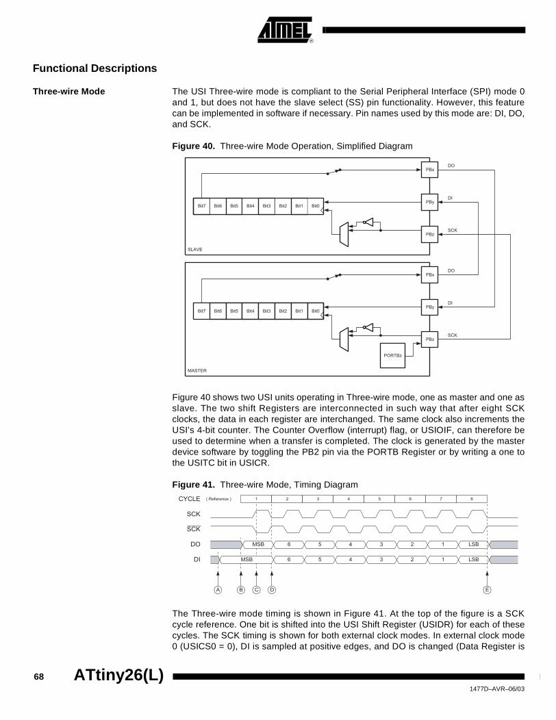
Functional Descriptions
Three-wire Mode The USI Three-wire mode is compliant to the Serial Peripheral Interface (SPI) mode 0and 1, but does not have the slave select (SS) pin functionality. However, this featurecan be implemented in software if necessary. Pin names used by this mode are: DI, DO,and SCK.
Figure 40. Three-wire Mode Operation, Simplified Diagram
Figure 40 shows two USI units operating in Three-wire mode, one as master and one asslave. The two shift Registers are interconnected in such way that after eight SCKclocks, the data in each register are interchanged. The same clock also increments theUSI’s 4-bit counter. The Counter Overflow (interrupt) flag, or USIOIF, can therefore beused to determine when a transfer is completed. The clock is generated by the masterdevice software by toggling the PB2 pin via the PORTB Register or by writing a one tothe USITC bit in USICR.
Figure 41. Three-wire Mode, Timing Diagram
The Three-wire mode timing is shown in Figure 41. At the top of the figure is a SCKcycle reference. One bit is shifted into the USI Shift Register (USIDR) for each of thesecycles. The SCK timing is shown for both external clock modes. In external clock mode0 (USICS0 = 0), DI is sampled at positive edges, and DO is changed (Data Register is
SLAVE
MASTER
Bit7 Bit6 Bit5 Bit4 Bit3 Bit2 Bit1 Bit0 PBy
PBx
PBz
DO
DI
SCK
Bit7 Bit6 Bit5 Bit4 Bit3 Bit2 Bit1 Bit0 PBy
PBx
PBz
DO
DI
SCK
PORTBz
MSB
MSB
6 5 4 3 2 1 LSB
1 2 3 4 5 6 7 8
6 5 4 3 2 1 LSB
SCK
SCK
DO
DI
DCBA E
CYCLE ( Reference )
68 ATtiny26(L) 1477D–AVR–06/03

ATtiny26(L)
shifted by one) at negative edges. External clock mode 1 (USICS0 = 1) uses the oppo-site edges versus mode 0, i.e., samples data at negative and changes the output atpositive edges. The USI clock modes corresponds to the SPI data mode 0 and 1.
Referring to the timing diagram (Figure 41.), a bus transfer involves the following steps:
1. The slave device and master device sets up its data output and, depending on the protocol used, enables its output driver (mark A and B). The output is set up by writing the data to be transmitted to the serial Data Register. Enabling of the output is done by setting the corresponding bit in the port data direction register (DDRB2). Note that point A and B does not have any specific order, but both must be at least one half SCK cycle before point C where the data is sampled. This must be done to ensure that the data setup requirement is satisfied. The 4-bit counter is reset to zero.
2. The master generates a clock pulse by software toggling the SCK line twice (C and D). The bit value on the slave and master’s data input (DI) pin is sampled by the USI on the first edge (C), and the data output is changed on the opposite edge (D). The 4-bit counter will count both edges.
3. Step 2. is repeated eight times for a comlpete register (byte) transfer.
4. After eight clock pulses (i.e., 16 clock edges) the counter will overflow and indi-cate that the transfer is completed. The data bytes transferred must now be processed before a new transfer can be initiated. The overflow interrupt will wake up the processor if it is set to Idle mode. Depending of the protocol used the slave device can now set its output to high impedance.
SPI Master Operation Example
The following code demonstrates how to use the USI module as a SPI master:SPITransfer:
out USIDR,r16
ldi r16,(1<<USIOIF)
out USISR,r16
ldi r16,(1<<USIWM0)+(1<<USICS1)+(1<<USICLK)+(1<<USITC)
SPITransfer_loop:
out USICR,r16
sbis USISR,USIOIF
rjmp SPITransfer_loop
in r16,USIDR
ret
The code is size optimized using only 8 instructions (+ ret). The code example assumesthat the DO and SCK pins are enabled as output in the DDRB Register. The valuestored in register r16 prior to the function is called is transferred to the slave device, andwhen the transfer is completed the data received from the slave is stored back into ther16 register.
The second and third instructions clears the USI Counter Overflow Flag and the USIcounter value. The fourth and fifth instruction set Three-wire mode, positive edge ShiftRegister clock, count at USITC strobe, and toggle SCK (PORTB2). The loop is repeated16 times.
691477D–AVR–06/03

The following code demonstrates how to use the USI module as a SPI Master with max-imum speed (fsck = fck/2):
SPITransfer_Fast:
out USIDR,r16
ldi r16,(1<<USIWM0)+(0<<USICS0)+(1<<USITC)
ldi r17,(1<<USIWM0)+(0<<USICS0)+(1<<USITC)+(1<<USICLK)
out USICR,r16 ; MSB
out USICR,r17
out USICR,r16
out USICR,r17
out USICR,r16
out USICR,r17
out USICR,r16
out USICR,r17
out USICR,r16
out USICR,r17
out USICR,r16
out USICR,r17
out USICR,r16
out USICR,r17
out USICR,r16 ; LSB
out USICR,r17
in r16,USIDR
ret
SPI Slave Operation Example The following code demonstrates how to use the USI module as a SPI slave:init:
ldi r16,(1<<USIWM0)+(1<<USICS1)
out USICR,r16
...
SlaveSPITransfer:
out USIDR,r16
ldi r16,(1<<USIOIF)
out USISR,r16
SlaveSPITransfer_loop:
sbis USISR,USIOIF
rjmp SlaveSPITransfer_loop
in r16,USIDR
ret
The code is size optimized using only 8 instructions (+ ret). The code example assumesthat the DO is configured as output and SCK pin is configured as input in the DDRBRegister. The value stored in register r16 prior to the function is called is transferred tothe master device, and when the transfer is completed the data received from the mas-ter is stored back into the r16 register.
70 ATtiny26(L) 1477D–AVR–06/03

ATtiny26(L)
Note that the first two instructions is for initialization only and needs only to be executedonce.These instructions sets Three-wire mode and positive edge Shift Register clock.The loop is repeated until the USI Counter Overflow Flag is set.
Two-wire Mode The USI Two-wire mode is compliant to the Inter IC (TWI) bus protocol, but without slewrate limiting on outputs and input noise filtering. Pin names used by this mode are SCLand SDA.
Figure 42. Two-wire Mode Operation, Simplified Diagram
Figure 42 shows two USI units operating in Two-wire mode, one as master and one asslave. It is only the physical layer that is shown since the system operation is highlydependent of the communication scheme used. The main differences between the mas-ter and slave operation at this level, is the serial clock generation which is always doneby the master, and only the slave uses the clock control unit. Clock generation must beimplemented in software, but the shift operation is done automatically by both devices.Note that only clocking on negative edge for shifting data is of practical use in this mode.The slave can insert wait states at start or end of transfer by forcing the SCL clock low.This means that the master must always check if the SCL line was actually releasedafter it has generated a positive edge.
Since the clock also increments the counter, a counter overflow can be used to indicatethat the transfer is completed. The clock is generated by the master by toggling the PB2pin via the PORTB Register.
The data direction is not given by the physical layer. A protocol, like the one used by theTWI-bus, must be implemented to control the data flow.
MASTER
SLAVE
Bit7 Bit6 Bit5 Bit4 Bit3 Bit2 Bit1 Bit0 PBy
PBz
SDA
SCL
Bit7 Bit6 Bit5 Bit4 Bit3 Bit2 Bit1 Bit0
Two-wire ClockControl Unit
PBy
PBz
HOLDSCL
PORTBz
SDA
SCL
VCC
711477D–AVR–06/03

Figure 43. Two-wire Mode, Typical Timing Diagram
Referring to the timing diagram (Figure 43.), a bus transfer involves the following steps:
1. The a start condition is generated by the master by forcing the SDA low line while the SCL line is high (A). SDA can be forced low either by writing a zero to bit 7 of the Shift Register, or by setting the PORTB0 bit to zero. Note that DDRB0 must be set to one for the output to be enabled. The slave device’s start detector logic (Figure 44.) detects the start condition and sets the USISIF flag. The flag can generate an interrupt if necessary.
2. In addition, the start detector will hold the SCL line low after the master has forced an negative edge on this line (B). This allows the slave to wake up from sleep or complete its other tasks, before setting up the Shift Register to receive the address by clearing the start condition flag and reset the counter.
3. The master set the first bit to be transferred and releases the SCL line (C). The slave samples the data and shift it into the serial register at the positive edge of the SCL clock.
4. After eight bits are transferred containing slave address and data direction (read or write), the slave counter overflows and the SCL line is forced low (D). If the slave is not the one the master has addressed it releases the SCL line and waits for a new start condition.
5. If the slave is addressed it holds the SDA line low during the acknowledgment cycle before holding the SCL line low again (i.e., the Counter Register must be set to 14 before releasing SCL at (D)). Depending of the R/W bit the master or slave enables its output. If the bit is set, a master read operation is in progress (i.e., the slave drives the SDA line) The slave can hold the SCL line low after the acknowledge (E).
6. Multiple bytes can now be transmitted, all in same direction, until a stop condition is given by the master (F). Or a new start condition is given.
If the slave is not able to receive more data it does not acknowledge the data byte it haslast received. When the master does a read operation it must terminate the operation byforce the acknowledge bit low after the last byte transmitted.
Figure 44. Start Condition Detector, Logic Diagram
PS ADDRESS
1 - 7 8 9
R/W ACK ACK
1 - 8 9
DATA ACK
1 - 8 9
DATA
SDA
SCL
A B D EC F
SDA
SCLWrite( USISIF)
CLOCKHOLD
USISIF
D Q
CLR
D Q
CLR
72 ATtiny26(L) 1477D–AVR–06/03

ATtiny26(L)
Start Condition Detector The start condition detector is shown in Figure 44. The SDA line is delayed (in the rangeof 50 to 300 ns) to ensure valid sampling of the SCL line. The start condition detector isonly enabled in Two-wire mode.
The start condition detector is working asynchronously and can therefore wake up theprocessor from the Power-down sleep mode. However, the protocol used might haverestrictions on the SCL hold time. Therefore, when using this feature in this case theoscillator start-up time set by the CKSEL Fuses (see “Clock Systems and their Distribu-tion” on page 25) must also be taken into the consideration. Refer to the description of“Bit 7 – USISIF: Start Condition Interrupt Flag” on page 64 for further details.
Alternative USI Usage When the USI unit is not used for serial communication, it can be set up to do alternativetasks due to its flexible design.
Half-duplex Asynchronous Data Transfer
By utilizing the Shift Register in Three-wire mode, it is possible to implement a morecompact and higher performance UART than by software only.
4-bit Counter The 4-bit counter can be used as a stand-alone counter with overflow interrupt. Notethat if the counter is clocked externally, both clock edges will generate an increment.
12-bit Timer/Counter Combining the USI 4-bit counter and Timer/Counter0 allows them to be used as a 12-bitcounter.
Edge Triggered External Interrupt
By setting the counter to maximum value (F) it can function as an additional externalinterrupt. The overflow flag and interrupt enable bit are then used for the external inter-rupt. This feature is selected by the USICS1 bit.
Software Interrupt The counter overflow interrupt can be used as a software interrupt triggered by a clockstrobe.
731477D–AVR–06/03

Analog Comparator The Analog Comparator compares the input values on the positive pin PA6 (AIN0) andnegative pin PA7 (AIN1). When the voltage on the positive pin PA6 (AIN0) is higher thanthe voltage on the negative pin PA7 (AIN1), the Analog Comparator Output, ACO is set(one). The comparator’s output can trigger a separate interrupt, exclusive to the AnalogComparator. The user can select Interrupt triggering on comparator output rise, fall ortoggle. A block diagram of the comparator and its surrounding logic is shown in the Fig-ure 45.
Figure 45. Analog Comparator Block Diagram
Analog Comparator Control and Status Register – ACSR
• Bit 7 – ACD: Analog Comparator Disable
When this bit is set(one), the power to the Analog Comparator is switched off. This bitcan be set at any time to turn off the Analog Comparator. When changing the ACD bit,the Analog Comparator Interrupt must be disabled by clearing the ACIE bit in ACSR.Otherwise an interrupt can occur when the bit is changed.
• Bit 6 – ACBG: Analog Comparator Bandgap Select
When this bit is set (one), it selects internal bandgap reference voltage (1.18V) as thepositive comparator input.
• Bit 5 – ACO: Analog Comparator Output
ACO is directly connected to the comparator output.
PA6(AIN0)
PA7
MUX
MUX
MUX
ADCMULTIPLEXER OUTPUT
(AIN1)
ACBG
ACME
Bit 7 6 5 4 3 2 1 0
$08 ($28) ACD ACBG ACO ACI ACIE ACME ACIS1 ACIS0 ACSR
Read/Write R/W R/W R R/W R/W R/W R/W R/W
Initial Value 0 0 X 0 0 0 0 0
74 ATtiny26(L) 1477D–AVR–06/03
ATtiny26(L)
• Bit 4 – ACI: Analog Comparator Interrupt Flag
This bit is set (one) when a comparator output event triggers the interrupt mode definedby ACI1 and ACI0. The Analog Comparator Interrupt routine is executed if the ACIE bitis set (one) and the I-bit in SREG is set (one). ACI is cleared by hardware when execut-ing the corresponding interrupt handling vector. Alternatively, ACI is cleared by writing alogic one to the flag.
• Bit 3 – ACIE: Analog Comparator Interrupt Enable
When the ACIE bit is set (one) and the I-bit in the Status Register is set (one), the Ana-log Comparator interrupt is activated. When cleared (zero), the interrupt is disabled.
• Bit 2 – ACME: Analog Comparator Multiplexer Enable
When the ACME bit is set (one) and the ADC is switched off (ADEN in ADCSR is zero),MUX3...0 in ADMUX select the input pin to replace the negative input to the AnalogComparator, as shown in Table 33 on page 76. If ACME is cleared (zero) or ADEN is set(one), PA7(AIN1) is applied to the negative input to the Analog Comparator.
• Bits 1, 0 – ACIS1, ACIS0: Analog Comparator Interrupt Mode Select
These bits determine which comparator events that trigger the Analog Comparator inter-rupt. The different settings are shown in Table 32.
Note: 1. When changing the ACIS1/ACIS0 bits, the Analog Comparator Interrupt must be dis-abled by clearing its Interrupt Enable bit in the ACSR Register. Otherwise an interruptcan occur when the bits are changed.
Table 32. ACIS1/ACIS0 Settings(1)
ACIS1 ACIS0 Interrupt Mode
0 0 Comparator Interrupt on Output Toggle
0 1 Reserved
1 0 Comparator Interrupt on Falling Output Edge
1 1 Comparator Interrupt on Rising Output Edge
751477D–AVR–06/03
Notes: 1. MUX4 does not affect Analog Comparator input selection.2. Pin change interrupt on PA6 and PA7 is disabled if the Analog Comparator is
enabled. This happens regardless of whether AIN1 or AIN0 has been replaced asinputs to the Analog Comparator.
3. The MUX3...0 selections go into effect after one clock cycle delay.
Table 33. Analog Comparator Input Selection(1)
ACME ADEN MUX3...0(3) Analog Comparator Negative Input
0 X XXXX AIN1
1 1 XXXX AIN1
1 0 0000 ADC0
1 0 0001 ADC1
1 0 0010 ADC2
1 0 0011 ADC3
1 0 0100 ADC4
1 0 0101 ADC5
1 0 0110 ADC6(2)
1 0 0111 ADC7(2)
1 0 1000 ADC8
1 0 1001 ADC9
1 0 1010 ADC10
1 0 1011 Undefined
1 0 1100 Undefined
1 0 1101 Undefined
1 0 1110 Undefined
1 0 1111 Undefined
76 ATtiny26(L) 1477D–AVR–06/03

ATtiny26(L)
Analog to Digital Converter
Features • 10-bit Resolution• ±2 LSB Absolute Accuracy• 0.5 LSB Integral Non-linearity• Optional Offset Cancellation• 65 - 260 µs Conversion Time• 11 Multiplexed Single Ended Input Channels• 8 Differential Input Channels• 7 Differential Input Channels with Optional Gain of 20x• Optional Left Adjustment for ADC Result Readout• 0 - AVCC ADC Input Voltage Range• Selectable ADC Reference Voltage• Free Running or Single Conversion Mode• Interrupt on ADC Conversion Complete• Sleep Mode Noise Canceler
The ATtiny26(L) features a 10-bit successive approximation ADC. The ADC is con-nected to an 11-channel Analog Multiplexer which allows eight differential voltage inputcombinations or 11 single-ended voltage inputs constructed from seven pins from Port Aand four pins from Port B. Seven of the differential inputs are equipped with a program-mable gain stage, providing amplification steps of 0 dB (1x) and 26 dB (20x) on thedifferential input voltage before the A/D conversion. There are four groups of three dif-ferential analog input channel selections. All input channels in each group share acommon negative terminal, while another ADC input can be selected as the positiveinput terminal. The single-ended voltage inputs refer to 0V (GND).
The ADC contains a Sample and Hold Amplifier which ensures that the input voltage tothe ADC is held at a constant level during conversion. A block diagram of the ADC isshown in Figure 46.
The ADC has an analog supply voltage pin, AVCC. The voltage on AVCC must not differmore than ±0.3V from VCC. See the paragraph “ADC Noise Canceling Techniques” onpage 88 on how to connect these pins.
An internal reference voltage of nominally 2.56V is provided On-chip, and this referencemay be externally decoupled at the AREF pin by a capacitor.
771477D–AVR–06/03
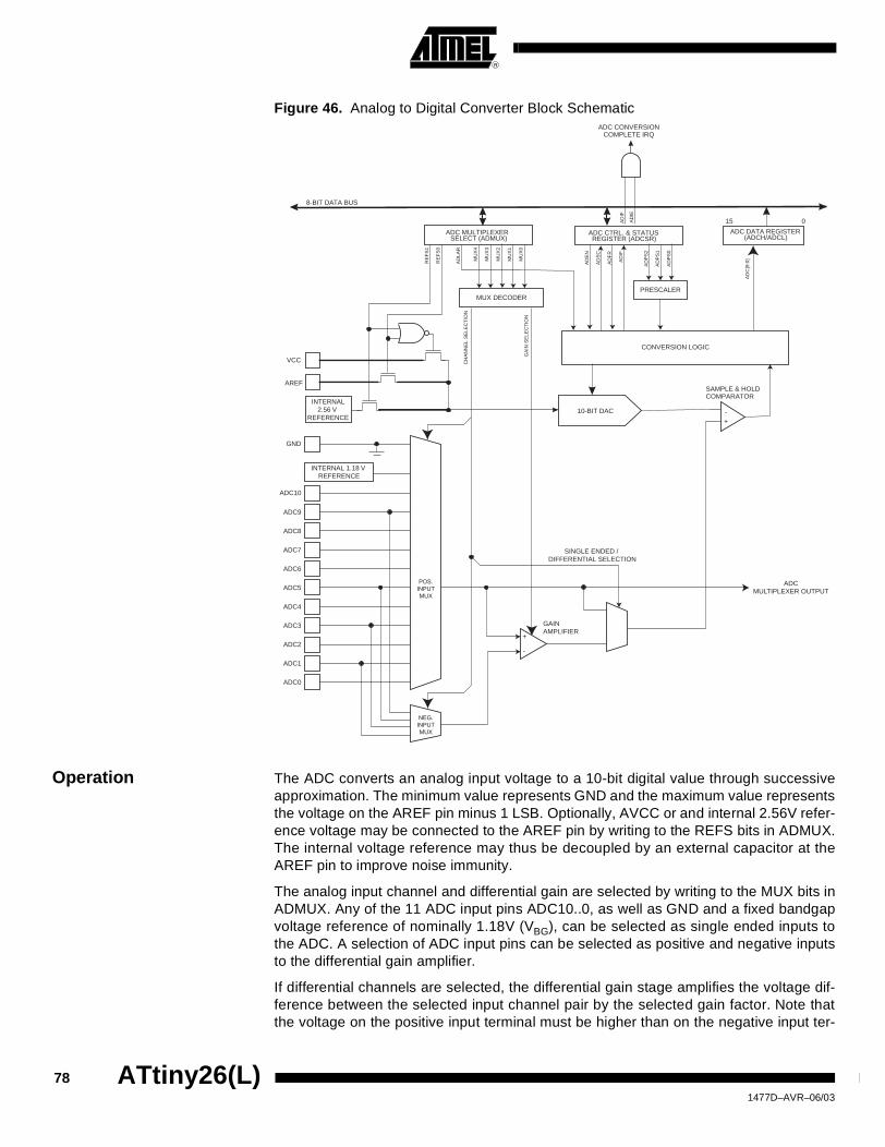
Figure 46. Analog to Digital Converter Block Schematic
Operation The ADC converts an analog input voltage to a 10-bit digital value through successiveapproximation. The minimum value represents GND and the maximum value representsthe voltage on the AREF pin minus 1 LSB. Optionally, AVCC or and internal 2.56V refer-ence voltage may be connected to the AREF pin by writing to the REFS bits in ADMUX.The internal voltage reference may thus be decoupled by an external capacitor at theAREF pin to improve noise immunity.
The analog input channel and differential gain are selected by writing to the MUX bits inADMUX. Any of the 11 ADC input pins ADC10..0, as well as GND and a fixed bandgapvoltage reference of nominally 1.18V (VBG), can be selected as single ended inputs tothe ADC. A selection of ADC input pins can be selected as positive and negative inputsto the differential gain amplifier.
If differential channels are selected, the differential gain stage amplifies the voltage dif-ference between the selected input channel pair by the selected gain factor. Note thatthe voltage on the positive input terminal must be higher than on the negative input ter-
ADC CONVERSIONCOMPLETE IRQ
8-BIT DATA BUS
15 0
ADC MULTIPLEXERSELECT (ADMUX)
ADC CTRL. & STATUSREGISTER (ADCSR)
ADC DATA REGISTER(ADCH/ADCL)
MU
X2
AD
IE
AD
FR
AD
SC
AD
EN
AD
IFA
DIF
MU
X1
MU
X0
AD
PS
0
AD
PS
1
AD
PS
2
MU
X3
CONVERSION LOGIC
10-BIT DAC
+-
SAMPLE & HOLDCOMPARATOR
MUX DECODER
MU
X4
ADC7
ADC6
ADC5
ADC4
ADC3
ADC2
ADC1
ADC0
RE
FS
0
RE
FS
1
AD
LAR
+
-
CH
AN
NE
L S
ELE
CT
ION
GA
IN S
ELE
CT
ION
AD
C[9
:0]
ADCMULTIPLEXER OUTPUT
GAINAMPLIFIER
INTERNAL 1.18 V REFERENCE
PRESCALER
SINGLE ENDED / DIFFERENTIAL SELECTION
GND
POS.INPUTMUX
NEG.INPUTMUX
ADC10
ADC9
ADC8
INTERNAL2.56 V
REFERENCE
VCC
AREF
78 ATtiny26(L) 1477D–AVR–06/03
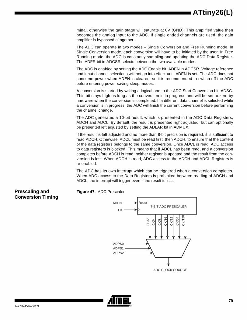
ATtiny26(L)
minal, otherwise the gain stage will saturate at 0V (GND). This amplified value thenbecomes the analog input to the ADC. If single ended channels are used, the gainamplifier is bypassed altogether.
The ADC can operate in two modes – Single Conversion and Free Running mode. InSingle Conversion mode, each conversion will have to be initiated by the user. In FreeRunning mode, the ADC is constantly sampling and updating the ADC Data Register.The ADFR bit in ADCSR selects between the two available modes.
The ADC is enabled by setting the ADC Enable bit, ADEN in ADCSR. Voltage referenceand input channel selections will not go into effect until ADEN is set. The ADC does notconsume power when ADEN is cleared, so it is recommended to switch off the ADCbefore entering power saving sleep modes.
A conversion is started by writing a logical one to the ADC Start Conversion bit, ADSC.This bit stays high as long as the conversion is in progress and will be set to zero byhardware when the conversion is completed. If a different data channel is selected whilea conversion is in progress, the ADC will finish the current conversion before performingthe channel change.
The ADC generates a 10-bit result, which is presented in the ADC Data Registers,ADCH and ADCL. By default, the result is presented right adjusted, but can optionallybe presented left adjusted by setting the ADLAR bit in ADMUX.
If the result is left adjusted and no more than 8-bit precision is required, it is sufficient toread ADCH. Otherwise, ADCL must be read first, then ADCH, to ensure that the contentof the data registers belongs to the same conversion. Once ADCL is read, ADC accessto data registers is blocked. This means that if ADCL has been read, and a conversioncompletes before ADCH is read, neither register is updated and the result from the con-version is lost. When ADCH is read, ADC access to the ADCH and ADCL Registers isre-enabled.
The ADC has its own interrupt which can be triggered when a conversion completes.When ADC access to the Data Registers is prohibited between reading of ADCH andADCL, the interrupt will trigger even if the result is lost.
Prescaling and Conversion Timing
Figure 47. ADC Prescaler
7-BIT ADC PRESCALER
ADC CLOCK SOURCE
CK
ADPS0ADPS1ADPS2
CK
/128
CK
/2
CK
/4
CK
/8
CK
/16
CK
/32
CK
/64
ResetADEN
791477D–AVR–06/03
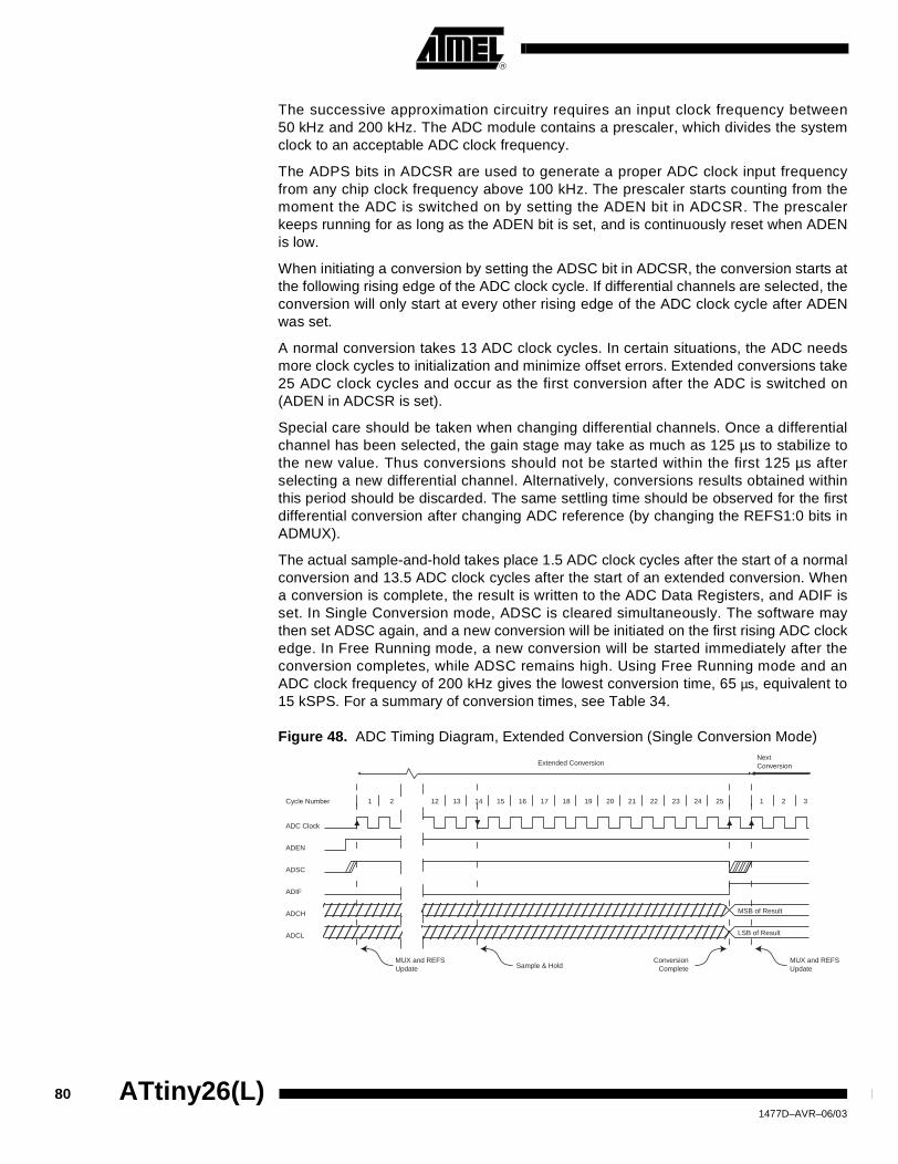
The successive approximation circuitry requires an input clock frequency between50 kHz and 200 kHz. The ADC module contains a prescaler, which divides the systemclock to an acceptable ADC clock frequency.
The ADPS bits in ADCSR are used to generate a proper ADC clock input frequencyfrom any chip clock frequency above 100 kHz. The prescaler starts counting from themoment the ADC is switched on by setting the ADEN bit in ADCSR. The prescalerkeeps running for as long as the ADEN bit is set, and is continuously reset when ADENis low.
When initiating a conversion by setting the ADSC bit in ADCSR, the conversion starts atthe following rising edge of the ADC clock cycle. If differential channels are selected, theconversion will only start at every other rising edge of the ADC clock cycle after ADENwas set.
A normal conversion takes 13 ADC clock cycles. In certain situations, the ADC needsmore clock cycles to initialization and minimize offset errors. Extended conversions take25 ADC clock cycles and occur as the first conversion after the ADC is switched on(ADEN in ADCSR is set).
Special care should be taken when changing differential channels. Once a differentialchannel has been selected, the gain stage may take as much as 125 µs to stabilize tothe new value. Thus conversions should not be started within the first 125 µs afterselecting a new differential channel. Alternatively, conversions results obtained withinthis period should be discarded. The same settling time should be observed for the firstdifferential conversion after changing ADC reference (by changing the REFS1:0 bits inADMUX).
The actual sample-and-hold takes place 1.5 ADC clock cycles after the start of a normalconversion and 13.5 ADC clock cycles after the start of an extended conversion. Whena conversion is complete, the result is written to the ADC Data Registers, and ADIF isset. In Single Conversion mode, ADSC is cleared simultaneously. The software maythen set ADSC again, and a new conversion will be initiated on the first rising ADC clockedge. In Free Running mode, a new conversion will be started immediately after theconversion completes, while ADSC remains high. Using Free Running mode and anADC clock frequency of 200 kHz gives the lowest conversion time, 65 µs, equivalent to15 kSPS. For a summary of conversion times, see Table 34.
Figure 48. ADC Timing Diagram, Extended Conversion (Single Conversion Mode)
MSB of Result
LSB of Result
ADC Clock
ADSC
Sample & Hold
ADIF
ADCH
ADCL
Cycle Number
ADEN
1 2 12 13 14 15 16 17 18 19 20 21 22 23 24 25 1 2
Extended ConversionNextConversion
3
MUX and REFSUpdate
MUX and REFSUpdate
ConversionComplete
80 ATtiny26(L) 1477D–AVR–06/03

ATtiny26(L)
Figure 49. ADC Timing Diagram, Single Conversion
Figure 50. ADC Timing Diagram, Free Running Conversion
Table 34. ADC Conversion Time
ConditionSample & Hold (Cycles from
Start of Conversion)Conversion
Time (Cycles)Conversion Time (µs)
Extended conversion 13.5 25 125 - 500
Normal conversions 1.5 13 65 - 260
1 2 3 4 5 6 7 8 9 10 11 12 13
MSB of Result
LSB of Result
ADC Clock
ADSC
ADIF
ADCH
ADCL
Cycle Number 1 2
One Conversion Next Conversion
3
Sample & Hold
MUX and REFSUpdate
ConversionComplete
MUX and REFSUpdate
11 12 13
MSB of Result
LSB of Result
ADC Clock
ADSC
ADIF
ADCH
ADCL
Cycle Number1 2
One Conversion Next Conversion
3 4
ConversionComplete
Sample & Hold
MUX and REFSUpdate
811477D–AVR–06/03
ADC Noise Canceler Function
The ADC features a noise canceler that enables conversion during ADC Noise Reduc-tion mode (see “Power Management and Sleep Modes” on page 41) to reduce noiseinduced from the CPU core and other I/O peripherals. If other I/O peripherals must beactive during conversion, this mode works equivalently for Idle mode. To make use ofthis feature, the following procedure should be used:
1. Make sure that the ADC is enabled and is not busy converting. Single Conver-sion mode must be selected and the ADC conversion complete interrupt must be enabled.ADEN = 1ADSC = 0ADFR = 0ADIE = 1
2. Enter ADC Noise Reduction mode (or Idle mode). The ADC will start a conver-sion once the CPU has been halted.
3. If no other interrupts occur before the ADC conversion completes, the ADC inter-rupt will wake up the CPU and execute the ADC Conversion Complete interrupt routine.
ADC Conversion Result After the conversion is complete (ADIF is high), the conversion result can be found inthe ADC Result Registers (ADCL, ADCH).
For single ended conversion, the result is
where VIN is the voltage on the selected input pin and VREF the selected voltage refer-ence (see Table 36 on page 84 and Table 37 on page 85). 0x000 represents analogground, and 0x3FF represents the selected reference voltage minus one LSB.
If differential channels are used, the result is
where VPOS is the voltage on the positive input pin, VNEG the voltage on the negativeinput pin, GAIN the selected gain factor, and VREF the selected voltage reference. Keepin mind that VPOS must be higher than VNEG, otherwise, the ADC value will saturate at0x000. Figure 51 shows the decoding of the differential input range.
Table 35 shows the resulting output codes if the differential input channel pair (ADCn -ADCm) is selected with a gain of GAIN and a reference voltage of VREF.
ADCVIN 1024⋅
VREF--------------------------=
ADCVPOS VNEG–( ) GAIN 1024⋅ ⋅
VREF---------------------------------------------------------------------------=
82 ATtiny26(L) 1477D–AVR–06/03

ATtiny26(L)
Figure 51. Differential Measurement Range
Example:
ADMUX = 0xEB (ADC0 - ADC1, 20x gain, 2.56V reference, left adjusted result)
Voltage on ADC0 is 400 mV, voltage on ADC1 is 300 mV.
ADCR = 1024 * 20 * (400 - 300) / 2560 = 800 = 0x320
ADCL will thus read 0x00, and ADCH will read 0xC8. Writing zero to ADLAR rightadjusts the result: ADCL = 0x20, ADCH = 0x03.
Table 35. Correlation Between Input Voltage and Output Codes
VADCn Read code Corresponding decimal value
VADCm + VREF /GAIN 0x3FF 1023
VADCm + (1023/1024) VREF /GAIN 0x3FF 1023
VADCm + (1022/1024) VREF /GAIN 0x3FE 1022
... ... ...
VADCm + (1/1024) VREF /GAIN 0x001 1
VADCm 0x000 0
0
Output Code
0x3FF
0x000
VREF/GAIN Differential InputVoltage (Volts)
831477D–AVR–06/03

ADC Multiplexer Selection Register – ADMUX
• Bit 7, 6 – REFS1, REFS0: Reference Selection Bits
These bits select the voltage reference for the ADC, as shown in Table 36. If these bitsare changed during a conversion, the change will not go in effect until this conversion iscomplete (ADIF in ADCSR is set). The user should disregard the first conversion resultafter changing these bits to obtain maximum accuracy. If differential channels are used,using AVCC or an external AREF higher than (AVCC - 0.2V) is not recommended, asthis will affect ADC accuracy. The internal voltage reference may not be used if anexternal reference voltage is being applied to the AREF pin.
• Bit 5 – ADLAR: ADC Left Adjust Result
The ADLAR bit affects the presentation of the ADC conversion result in the ADC DataRegister. If ADLAR is cleared, the result is right adjusted. If ADLAR is set, the result isleft adjusted. Changing the ADLAR bit will affect the ADC Data Register immediately,regardless of any ongoing conversions. For a complete description of this bit, see “ADCData Register – ADCL and ADCH” on page 87.
• Bits 4..0 – MUX4..MUX0: Analog Channel and Gain Selection Bits
The value of these bits selects which combination of analog inputs are connected to theADC. These bits also select the gain for the differential channels. See Table 37 fordetails. If these bits are changed during a conversion, the change will not go in effectuntil this conversion is complete (ADIF in ADCSR is set).
Bit 7 6 5 4 3 2 1 0
$07 ($27) REFS1 REFS0 ADLAR MUX4 MUX3 MUX2 MUX1 MUX0 ADMUX
Read/Write R/W R/W R/W R/W R/W R/W R/W R/W
Initial Value 0 0 0 0 0 0 0 0
Table 36. Voltage Reference Selections for ADC
REFS1 REFS0 Voltage Reference Selection
0 0 AVCC
0 1 AREF (PA3), Internal Vref turned off.
1 0 Internal Voltage Reference (2.56 V), AREF pin (PA3) not connected.
1 1Internal Voltage Reference (2.56 V) with external capacitor at AREF pin (PA3).
84 ATtiny26(L) 1477D–AVR–06/03

ATtiny26(L)
Note: 1. For offset measurements only. See “Offset Compensation Schemes” on page 88.
Table 37. Input Channel and Gain Selections
MUX4..0Single Ended
InputPositive Differential
InputNegative Differential
Input Gain
00000 ADC0
N/A
00001 ADC1
00010 ADC2
00011 ADC3
00100 ADC4
00101 ADC5
00110 ADC6
00111 ADC7
01000 ADC8
01001 ADC9
01010 ADC10
01011
N/A
ADC0 ADC1 20x
01100 ADC0 ADC1 1x
01101(1) ADC1 ADC1 20x
01110 ADC2 ADC1 20x
01111 ADC2 ADC1 1x
10000
N/A
ADC2 ADC3 1x
10001(1) ADC3 ADC3 20x
10010 ADC4 ADC3 20x
10011(1) ADC4 ADC3 1x
10100
N/A
ADC4 ADC5 20x
10101 ADC4 ADC5 1x
10110(1) ADC5 ADC5 20x
10111 ADC6 ADC5 20x
11000 ADC6 ADC5 1x
11001
N/A
ADC8 ADC9 20x
11010 ADC8 ADC9 1x
11011(1) ADC9 ADC9 20x
11100 ADC10 ADC9 20x
11101 ADC10 ADC9 1x
11110 1.18V (VBG)N/A
11111 0V (GND)
851477D–AVR–06/03

ADC Control and Status Register – ADCSR
• Bit 7 – ADEN: ADC Enable
Writing a logical “1” to this bit enables the ADC. By clearing this bit to zero, the ADC isturned off. Turning the ADC off while a conversion is in progress, will terminate thisconversion.
• Bit 6 – ADSC: ADC Start Conversion
In Single Conversion mode, a logical “1” must be written to this bit to start each conver-sion. In Free Running mode, a logical “1” must be written to this bit to start the firstconversion. The first time ADSC has been written after the ADC has been enabled, or ifADSC is written at the same time as the ADC is enabled, a dummy conversion will pre-cede the initiated conversion. This dummy conversion performs initialization of the ADC.
ADSC will read as one as long as a conversion is in progress. When the conversion iscomplete, it returns to zero. When a dummy conversion precedes a real conversion,ADSC will stay high until the real conversion completes. Writing a 0 to this bit has noeffect.
• Bit 5 – ADFR: ADC Free Running Select
When this bit is set (one) the ADC operates in Free Running mode. In this mode, theADC samples and updates the Data Registers continuously. Clearing this bit (zero) willterminate Free Running mode.
• Bit 4 – ADIF: ADC Interrupt Flag
This bit is set (one) when an ADC conversion completes and the data registers areupdated. The ADC Conversion Complete Interrupt is executed if the ADIE bit and the I-bit in SREG are set (one). ADIF is cleared by hardware when executing the correspond-ing interrupt handling vector. Alternatively, ADIF is cleared by writing a logical one to theflag. Beware that if doing a read-modify-write on ADCSR, a pending interrupt can be dis-abled. This also applies if the SBI and CBI instructions are used.
• Bit 3 – ADIE: ADC Interrupt Enable
When this bit is set (one) and the I-bit in SREG is set (one), the ADC Conversion Com-plete Interrupt is activated.
Bit 7 6 5 4 3 2 1 0
$06 ($26) ADEN ADSC ADFR ADIF ADIE ADPS2 ADPS1 ADPS0 ADCSR
Read/Write R/W R/W R/W R/W R/W R/W R/W R/W
Initial Value 0 0 0 0 0 0 0 0
86 ATtiny26(L) 1477D–AVR–06/03

ATtiny26(L)
• Bits 2..0 – ADPS2..0: ADC Prescaler Select Bits
These bits determine the division factor between the CK frequency and the input clockto the ADC.
ADC Data Register – ADCL and ADCH
ADLAR = 0
ADLAR = 1
When an ADC conversion is complete, the result is found in these two registers. TheADLAR bit in ADMUX affect the way the result is read from the registers. If ADLAR isset, the result is left adjusted. If ADLAR is cleared (default), the result is right adjusted. Ifthe result is left adjusted and no more than 8-bit precision is required, it is sufficient toread ADCH. Otherwise, ADCL must be read first, then ADCH.
• ADC9..0: ADC Conversion Result
These bits represent the result from the conversion. For differential channels, this is theabsolute value after gain adjustment, as indicated in Table 37 on page 85. For singleended channels, $000 represents analog ground, and $3FF represents the selected ref-erence voltage minus one LSB.
Table 38. ADC Prescaler Selections
ADPS2 ADPS1 ADPS0 Division Factor
0 0 0 2
0 0 1 2
0 1 0 4
0 1 1 8
1 0 0 16
1 0 1 32
1 1 0 64
1 1 1 128
Bit 15 14 13 12 11 10 9 8
$05 ($25) – – – – – – ADC9 ADC8 ADCH
$04 ($24) ADC7 ADC6 ADC5 ADC4 ADC3 ADC2 ADC1 ADC0 ADCL
7 6 5 4 3 2 1 0
Read/Write R R R R R R R R
R R R R R R R R
Initial Value 0 0 0 0 0 0 0 0
0 0 0 0 0 0 0 0
Bit 15 14 13 12 11 10 9 8
$05 ($25) ADC9 ADC8 ADC7 ADC6 ADC5 ADC4 ADC3 ADC2 ADCH
$04 ($24) ADC1 ADC0 – – – – – – ADCL
7 6 5 4 3 2 1 0
Read/Write R R R R R R R R
R R R R R R R R
Initial Value 0 0 0 0 0 0 0 0
0 0 0 0 0 0 0 0
871477D–AVR–06/03
Scanning Multiple Channels
Since change of analog channel always is delayed until a conversion is finished, theFree Running mode can be used to scan multiple channels without interrupting the con-verter. Typically, the ADC Conversion Complete interrupt will be used to perform thechannel shift. However, the user should take the following fact into consideration:
The interrupt triggers once the result is ready to be read. In Free Running mode, thenext conversioin will start immediately when the interrupt triggers. If ADMUX ischanged after the interrupt triggers, the next conversion has already started, and theold setting is used.
ADC Noise Canceling Techniques
Digital circuitry inside and outside the ATtiny26(L) generates EMI which might affect theaccuracy of analog measurements. If conversion accuracy is critical, the noise level canbe reduced by applying the following techniques:
1. The analog part of the ATtiny26(L) and all analog components in the application should have a separate analog ground plane on the PCB. This ground plane is connected to the digital ground plane via a single point on the PCB.
2. Keep analog signal paths as short as possible. Make sure analog tracks run over the analog ground plane, and keep them well away from high-speed switching digital tracks.
3. The AVCC pin on the ATtiny26(L) should be connected to the digital VCC supply voltage via an LC network as shown in Figure 52.
4. Use the ADC noise canceler function to reduce induced noise from the CPU.
5. If some pins are used as digital outputs, it is essential that these do not switch while a conversion is in progress in that port.
Offset Compensation Schemes
All active gain stages and differential-to-single-ended stages in front of the ADC have abuilt-in offset cancellation circuitry that nulls the offset of these stages as much aspossible.
In the case of unity gain differential measurements, the remaining worst case offset inthe differential to single-ended stage is less than 5 mV offset (typically 3 mV), or twoLSBs.
In the case of 20x gain differential measurements, the remaining worst case offset erroris in the range of 10 mV in the ADC conversion result. If the internal voltage reference(2.56V) is used during conversion of differential channels, one LSB of the 10-bit ADC is2.56 mV, i.e., the worst case error is approximately four LSBs. This error is fairly stableover short term, as temperature which is the main contributor to offset drift, variesslowly. Offset variation over the temperature range is in the order of 5 mV, i.e., approxi-mately two LSBs.
If better offset cancellation is desired, it is possible to select the same channel for bothdifferential input references and actually measure the offset from the complete analogpath. This offset residue can then be subtracted in software from the measurementresults. Using this kind of software based offset correction, offset on any channel can bereduced below one LSB.
88 ATtiny26(L) 1477D–AVR–06/03

ATtiny26(L)
Figure 52. ADC Power Connections
PA0 (ADC0)
(ADC10/RESET) PB7
(ADC9/INT0/T0) PB6
(ADC8/XTAL2) PB5
(ADC7/XTAL1) PB4
VCC
PA1 (ADC1)
PA2 (ADC2)
PA3 (AREF)
PA4 (ADC3)
PA5 (ADC4)
PA6 (ADC5/AIN0)
PA7 (ADC6/AIN1)
GND
AVCC
10µΗ
100n
FA
nalo
g G
roun
d P
lane
ATtiny26/L
2020
6
5
7
8
9
GND
10
16
14
13
12
11
18
19
15
17
1
3
2
4
(MOSI/DI/SDA/OC1A) PB0
(MISO/DO/OC1A) PB1
(SCK/SCL/OC1B) PB2
(OC1B) PB3
891477D–AVR–06/03

I/O Ports
Introduction All AVR ports have true Read-Modify-Write functionality when used as general digitalI/O ports. This means that the direction of one port pin can be changed without uninten-tionally changing the direction of any other pin with the SBI and CBI instructions. Thesame applies when changing drive value (if configured as output) or enabling/disablingof pull-up resistors (if configured as input). Each output buffer, except reset, has sym-metrical drive characteristics with both high sink and source capability. The pin driver isstrong enough to drive LED displays directly. All port pins have individually selectablepull-up resistors with a supply-voltage invariant resistance. All I/O pins have protectiondiodes to both VCC and Ground as indicated in Figure 53.
Figure 53. I/O Pin Equivalent Schematic
All registers and bit references in this section are written in general form. A lower case“x” represents the numbering letter for the port, and a lower case “n” represents the bitnumber. However, when using the register or bit defines in a program, the precise formmust be used. For example, PORTB3 for bit no. 3 in Port B, here documented generallyas PORTxn. The physical I/O Registers and bit locations are listed in “Register Descrip-tion for I/O Ports” on page 105.
Three I/O memory address locations are allocated for each port, one each for the DataRegister – PORTx, Data Direction Register – DDRx, and the Port Input Pins – PINx. ThePort Input Pins I/O location is read only, while the Data Register and the Data DirectionRegister are read/write. In addition, the Pull-up Disable – PUD bit in MCUCR disablesthe pull-up function for all pins in all ports when set.
Using the I/O port as General Digital I/O is described in “Ports as General Digital I/O” onpage 91. Most port pins are multiplexed with alternate functions for the peripheral fea-tures on the device. How each alternate function interferes with the port pin is describedin “Alternate Port Functions” on page 95. Refer to the individual module sections for afull description of the alternate functions.
Note that enabling the alternate function of some of the port pins does not affect the useof the other pins in the port as general digital I/O.
Cpin
Logic
Rpu
See Figure"General Digital I/O" for
Details
Pxn
90 ATtiny26(L) 1477D–AVR–06/03

ATtiny26(L)
Ports as General Digital I/O
The ports are bi-directional I/O ports with optional internal pull-ups. Figure 54 shows afunctional description of one I/O-port pin, here generically called Pxn.
Figure 54. General Digital I/O(1)
Note: 1. WPx, WDx, RRx, RPx, and RDx are common to all pins within the same port. clkI/O,SLEEP, and PUD are common to all ports.
Configuring the Pin Each port pin consists of 3 Register bits: DDxn, PORTxn, and PINxn. As shown in “Reg-ister Description for I/O Ports” on page 105, the DDxn bits are accessed at the DDRx I/Oaddress, the PORTxn bits at the PORTx I/O address, and the PINxn bits at the PINx I/Oaddress.
The DDxn bit in the DDRx Register selects the direction of this pin. If DDxn is writtenlogic one, Pxn is configured as an output pin. If DDxn is written logic zero, Pxn is config-ured as an input pin.
If PORTxn is written logic one when the pin is configured as an input pin, the pull-upresistor is activated. To switch the pull-up resistor off, PORTxn has to be written logiczero or the pin has to be configured as an output pin. The port pins are tri-stated when areset condition becomes active, even if no clocks are running.
If PORTxn is written logic one when the pin is configured as an output pin, the port pin isdriven high (one). If PORTxn is written logic zero when the pin is configured as an out-put pin, the port pin is driven low (zero).
When switching between tri-state (DDxn, PORTxn = 0b00) and output high (DDxn,PORTxn = 0b11), an intermediate state with either pull-up enabled (DDxn, PORTxn =0b01) or output low (DDxn, PORTxn = 0b10) must occur. Normally, the pull-upenabled state is fully acceptable, as a high-impedant environment will not notice the
clk
RPx
RRx
WPx
RDx
WDx
PUD
SYNCHRONIZER
WDx: WRITE DDRx
WPx: WRITE PORTxRRx: READ PORTx REGISTERRPx: READ PORTx PIN
PUD: PULLUP DISABLE
clkI/O: I/O CLOCK
RDx: READ DDRx
D
L
Q
Q
RESET
RESET
Q
QD
Q
Q D
CLR
PORTxn
Q
Q D
CLR
DDxn
PINxn
DAT
A B
US
SLEEP
SLEEP: SLEEP CONTROL
Pxn
I/O
911477D–AVR–06/03

difference between a strong high driver and a pull-up. If this is not the case, the PUD bitin the MCUCR Register can be set to disable all pull-ups in all ports.
Switching between input with pull-up and output low generates the same problem. Theuser must use either the tri-state (DDxn, PORTxn = 0b00) or the output high state(DDxn, PORTxn = 0b11) as an intermediate step.
Table 39 summarizes the control signals for the pin value.
Reading the Pin Value Independent of the setting of Data Direction bit DDxn, the port pin can be read throughthe PINxn Register Bit. As shown in Figure 54, the PINxn Register bit and the precedinglatch constitute a synchronizer. This is needed to avoid metastability if the physical pinchanges value near the edge of the internal clock, but it also introduces a delay. Figure55 shows a timing diagram of the synchronization when reading an externally appliedpin value. The maximum and minimum propagation delays are denoted tpd,max and tpd,minrespectively.
Figure 55. Synchronization when Reading an Externally Applied Pin Value
Consider the clock period starting shortly after the first falling edge of the system clock.The latch is closed when the clock is low, and goes transparent when the clock is high,as indicated by the shaded region of the “SYNC LATCH” signal. The signal value islatched when the system clock goes low. It is clocked into the PINxn Register at the suc-ceeding positive clock edge. As indicated by the two arrows tpd,max and tpd,min, a single
Table 39. Port Pin Configurations
DDxn PORTxnPUD
(in MCUCR) I/O Pull-up Comment
0 0 X Input No Tri-state (Hi-Z)
0 1 0 Input YesPxn will source current if ext. pulled low
0 1 1 Input No Tri-state (Hi-Z)
1 0 X Output No Output Low (Sink)
1 1 X Output No Output High (Source)
XXX in r17, PINx
0x00 0xFF
INSTRUCTIONS
SYNC LATCH
PINxn
r17
XXX
SYSTEM CLK
tpd, max
tpd, min
92 ATtiny26(L) 1477D–AVR–06/03

ATtiny26(L)
signal transition on the pin will be delayed between ½ and 1½ system clock perioddepending upon the time of assertion.
When reading back a software assigned pin value, a nop instruction must be inserted asindicated in Figure 56. The out instruction sets the “SYNC LATCH” signal at the positiveedge of the clock. In this case, the delay tpd through the synchronizer is one systemclock period.
Figure 56. Synchronization when Reading a Software Assigned Pin Value
out PORTx, r16 nop in r17, PINx
0xFF
0x00 0xFF
SYSTEM CLK
r16
INSTRUCTIONS
SYNC LATCH
PINxn
r17
t pd
931477D–AVR–06/03

The following code example shows how to set port B pins 0 and 1 high, 2 and 3 low, anddefine the port pins from 4 to 7 as input with pull-ups assigned to port pins 6 and 7. Theresulting pin values are read back again, but as previously discussed, a nop instructionis included to be able to read back the value recently assigned to some of the pins.
Note: 1. For the assembly program, two temporary registers are used to minimize the timefrom pull-ups are set on pins 0, 1, 6, and 7, until the direction bits are correctly set,defining bit 2 and 3 as low and redefining bits 0 and 1 as strong high drivers.
Digital Input Enable and Sleep Modes
As shown in Figure 54, the digital input signal can be clamped to ground at the input ofthe schmitt-trigger. The signal denoted SLEEP in the figure, is set by the MCU SleepController in Power-down mode, Standby mode, and ADC Noise Reduction mode toavoid high power consumption if some input signals are left floating, or have an analogsignal level close to VCC/2.
SLEEP is overridden for port pins enabled as External Interrupt pins. If the ExternalInterrupt Request is not enabled, SLEEP is active also for these pins. SLEEP is alsooverridden by various other alternate functions as described in “Alternate Port Func-tions” on page 95.
If a logic high level (“one”) is present on an Asynchronous External Interrupt pin config-ured as “Interrupt on a Rising Edge, Falling Edge, or Any Logic Change on Pin” whilethe external interrupt is not enabled, the corresponding External Interrupt Flag will be setwhen resuming from the above mentioned sleep modes, as the clamping in these sleepmodes produces the requested logic change.
Assembly Code Example(1)
...
; Define pull-ups and set outputs high
; Define directions for port pins
ldi r16,(1<<PB7)|(1<<PB6)|(1<<PB1)|(1<<PB0)
ldi r17,(1<<DDB3)|(1<<DDB2)|(1<<DDB1)|(1<<DDB0)
out PORTB,r16
out DDRB,r17
; Insert nop for synchronization
nop
; Read port pins
in r16,PINB
...
C Code Example
unsigned char i;
...
/* Define pull-ups and set outputs high */
/* Define directions for port pins */
PORTB = (1<<PB7)|(1<<PB6)|(1<<PB1)|(1<<PB0);
DDRB = (1<<DDB3)|(1<<DDB2)|(1<<DDB1)|(1<<DDB0);
/* Insert nop for synchronization*/
_NOP();
/* Read port pins */
i = PINB;
...
94 ATtiny26(L) 1477D–AVR–06/03
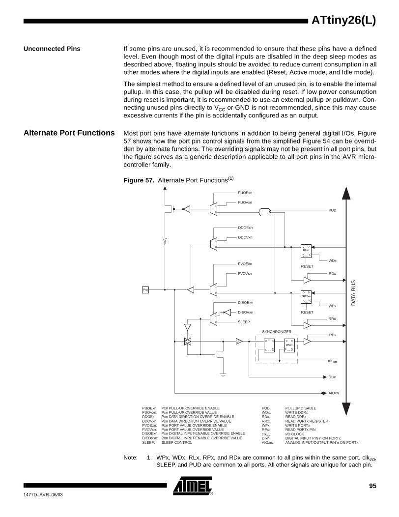
ATtiny26(L)
Unconnected Pins If some pins are unused, it is recommended to ensure that these pins have a definedlevel. Even though most of the digital inputs are disabled in the deep sleep modes asdescribed above, floating inputs should be avoided to reduce current consumption in allother modes where the digital inputs are enabled (Reset, Active mode, and Idle mode).
The simplest method to ensure a defined level of an unused pin, is to enable the internalpullup. In this case, the pullup will be disabled during reset. If low power consumptionduring reset is important, it is recommended to use an external pullup or pulldown. Con-necting unused pins directly to VCC or GND is not recommended, since this may causeexcessive currents if the pin is accidentally configured as an output.
Alternate Port Functions Most port pins have alternate functions in addition to being general digital I/Os. Figure57 shows how the port pin control signals from the simplified Figure 54 can be overrid-den by alternate functions. The overriding signals may not be present in all port pins, butthe figure serves as a generic description applicable to all port pins in the AVR micro-controller family.
Figure 57. Alternate Port Functions(1)
Note: 1. WPx, WDx, RLx, RPx, and RDx are common to all pins within the same port. clkI/O,SLEEP, and PUD are common to all ports. All other signals are unique for each pin.
clk
RPx
RRx
WPx
RDx
WDx
PUD
SYNCHRONIZER
WDx: WRITE DDRx
WPx: WRITE PORTxRRx: READ PORTx REGISTER
RPx: READ PORTx PIN
PUD: PULLUP DISABLE
clkI/O: I/O CLOCK
RDx: READ DDRx
D
L
Q
Q
SET
CLR
0
1
0
1
0
1
DIxn
AIOxn
DIEOExn
PVOVxn
PVOExn
DDOVxn
DDOExn
PUOExn
PUOVxn
PUOExn: Pxn PULL-UP OVERRIDE ENABLEPUOVxn: Pxn PULL-UP OVERRIDE VALUEDDOExn: Pxn DATA DIRECTION OVERRIDE ENABLEDDOVxn: Pxn DATA DIRECTION OVERRIDE VALUEPVOExn: Pxn PORT VALUE OVERRIDE ENABLEPVOVxn: Pxn PORT VALUE OVERRIDE VALUE
DIxn: DIGITAL INPUT PIN n ON PORTxAIOxn: ANALOG INPUT/OUTPUT PIN n ON PORTx
RESET
RESET
Q
Q D
CLR
Q
Q D
CLR
Q
QD
CLR
PINxn
PORTxn
DDxn
DAT
A B
US
0
1DIEOVxn
SLEEP
DIEOExn: Pxn DIGITAL INPUT-ENABLE OVERRIDE ENABLEDIEOVxn: Pxn DIGITAL INPUT-ENABLE OVERRIDE VALUESLEEP: SLEEP CONTROL
Pxn
I/O
951477D–AVR–06/03

Table 40 summarizes the function of the overriding signals. The pin and port indexesfrom Figure 57 are not shown in the succeeding tables. The overriding signals are gen-erated internally in the modules having the alternate function.
The following subsections shortly describes the alternate functions for each port, andrelates the overriding signals to the alternate function. Refer to the alternate functiondescription for further details.
Table 40. Generic Description of Overriding Signals for Alternate Functions
Signal Name Full Name Description
PUOE Pull-up Override Enable
If this signal is set, the pull-up enable is controlled by the PUOV signal. If this signal is cleared, the pull-up is enabled when DDxn, PORTxn, PUD = 0b010.
PUOV Pull-up Override Value
If PUOE is set, the pull-up is enabled/disabled when PUOV is set/cleared, regardless of the setting of the DDxn, PORTxn, and PUD Register bits.
DDOE Data Direction Override Enable
If this signal is set, the Output Driver Enable is controlled by the DDOV signal. If this signal is cleared, the Output driver is enabled by the DDxn Register bit.
DDOV Data Direction Override Value
If DDOE is set, the Output Driver is enabled/disabled when DDOV is set/cleared, regardless of the setting of the DDxn Register bit.
PVOE Port Value Override Enable
If this signal is set and the Output Driver is enabled, the port value is controlled by the PVOV signal. If PVOE is cleared, and the Output Driver is enabled, the port Value is controlled by the PORTxn Register bit.
PVOV Port Value Override Value
If PVOE is set, the port value is set to PVOV, regardless of the setting of the PORTxn Register bit.
DIEOE Digital Input Enable Override Enable
If this bit is set, the Digital Input Enable is controlled by the DIEOV signal. If this signal is cleared, the Digital Input Enable is determined by MCU-state (Normal mode, sleep modes).
DIEOV Digital Input Enable Override Value
If DIEOE is set, the Digital Input is enabled/disabled when DIEOV is set/cleared, regardless of the MCU state (Normal mode, sleep modes).
DI Digital Input This is the Digital Input to alternate functions. In the figure, the signal is connected to the output of the schmitt trigger but before the synchronizer. Unless the Digital Input is used as a clock source, the module with the alternate function will use its own synchronizer.
AIO Analog Input/output This is the Analog Input/Output to/from alternate functions. The signal is connected directly to the pad, and can be used bidirectionally.
96 ATtiny26(L) 1477D–AVR–06/03
ATtiny26(L)
MCU Control Register – MCUCR
The MCU Control Register contains control bits for general MCU functions.
• Bit 6 – PUD: Pull-up Disable
When this bit is set (one), the pull-ups in the I/O ports are disabled even if the DDxn andPORTxn Registers are configured to enable the pull-ups (DDxn, PORTxn = 0b01). See“Configuring the Pin” on page 91 for more details about this feature.
Alternate Functions of Port A Port A has an alternate functions as analog inputs for the ADC and Analog Comparatorand pin change interrupt as shown in Table 41. If some Port A pins are configured asoutputs, it is essential that these do not switch when a conversion is in progress. Thismight corrupt the result of the conversion. The ADC is described in “Analog to DigitalConverter” on page 77. Analog Comparator is described in “Analog Comparator” onpage 74. Pin change interrupt triggers on pins PA7, PA6 and PA3 if interrupt is enabledand it is not masked by the alternate functions even if the pin is configured as an output.See details from “Pin Change Interrupt” on page 38.
Table 42 and Table 43 relates the alternate functions of Port A to the overriding signalsshown in Figure 57 on page 95. Thera are changes on PA7, PA6, and PA3 digitalinputs. PA3 output and pullup driver are also overridden.
• ADC6/AIN1 Port – A, Bit 7
AIN1: Analog Comparator Negative input and ADC6: ADC input channel 6. Configurethe port pin as input with the internal pull-up switched off to avoid the digital port functionfrom interfering with the function of the analog comparator or analog to digital converter.
PCINT1: Pin Change Interrupt 1 pin. Pin change interrupt is enabled on pin when globalinterrupt is enabled, pin change interrupt is enabled and the alternate function do notmask the interrupt. The masking alternate function is the Analog Comparator. Digitalinput is enabled on pin PA7 also in SLEEP modes, if the pin change interrupt is enabledand not masked by the alternate function.
Bit 7 6 5 4 3 2 1 0
$35 ($55) – PUD SE SM1 SM0 – ISC01 ISC00 MCUCR
Read/Write R R/W R/W R/W R/W R R/W R/W
Initial Value 0 0 0 0 0 0 0 0
Table 41. Port A Pins Alternate Functions
Port Pin Alternate Function
PA7 ADC6 (ADC input channel 6)AIN1 (Analog Comparator negative input)PCINT1 (Pin Change Interrupt 1)
PA6 ADC5 (ADC input channel 5)AIN0 (Analog Comparator positive input)PCINT1 (Pin Change Interrupt 1)
PA5 ADC4 (ADC input channel 4)
PA4 ADC3 (ADC input channel 3)
PA3 AREF (ADC external reference)PCINT1 (Pin Change Interrupt 1)
PA2 ADC2 (ADC input channel 2)
PA1 ADC1 (ADC input channel 1)
PA0 ADC0 (ADC input channel 0)
971477D–AVR–06/03

• ADC5/AIN0 Port – A, Bit 6
AIN0: Analog Comparator Positive input and ADC5: ADC input channel 5. Configure theport pin as input with the internal pull-up switched off to avoid the digital port functionfrom interfering with the function of the Analog Comparator or analog to digitalconverter.
PCINT1: Pin Change Interrupt 1 pin. Pin change interrupt is enabled on pin when globalinterrupt is enabled, pin change interrupt is enabled and the alternate function do notmask the interrupt. The masking alternate function is the Analog Comparator. Digitalinput is enabled on pin PA6 also in SLEEP modes, if the pin change interrupt is enabledand not masked by the alternate function.
• ADC4, ADC3 Port – A, Bit 5, 4
ADC4/ADC3: ADC Input Channel 4 and 3. Configure the port pins as inputs with theinternal pull-ups switched off to avoid the digital port function from interfering with thefunction of the analog to digital converter.
• AREF/PCINT1 Port – A, Bit 3
AREF: External Reference for ADC. Pullup and output driver are disabled on PA3 whenthe pin is used as an external reference or Internal Voltage Reference (2.56V) withexternal capacitor at the AREF pin by setting (one) the bit REFS0 in the ADC MultiplexerSelection Register (ADMUX).
PCINT1: Pin Change Interrupt 1 pin. Pin change interrupt is enabled on pin when globalinterrupt is enabled, pin change interrupt is enabled and the alternate function do notmask the interrupt. The masking alternate function is the pin usage as an analog refer-ence for the ADC. Digital input is enabled on pin PA3 also in SLEEP modes, if the pinchange interrupt is enabled and not masked by the alternate function.
Table 42. Overriding Signals for Alternate Functions in PA7..PA4
Signal Name
PA7/ADC6/AIN1/PCINT1
PA6/ADC5/AIN0/PCINT1 PA5/ADC4 PA4/ADC3
PUOE 0 0 0 0
PUOV 0 0 0 0
DDOE 0 0 0 0
DDOV 0 0 0 0
PVOE 0 0 0 0
PVOV 0 0 0 0
DIEOE PCINT1_ENABLE(1) • ACSR[ACD]
PCINT1_ENABLE(1)• ACSR[ACD]
0 0
DIEOV 1 1 0 0
DI PCINT1 PCINT1 – –
AIO ADC6 INPUT, AIN1 ADC5 INPUT, AIN0 ADC4 INPUT ADC3 INPUT
98 ATtiny26(L) 1477D–AVR–06/03

ATtiny26(L)
Notes: 1. Note that the PCINT1 Interrupt is only enabled if both the Global Interrupt Flag isenabled, the PCIE1 flag in GIMSK is set and the alternate function of the pin is dis-abled as described in “Pin Change Interrupt” on page 38
2. Not operator is marked with “~”.
Table 43. Overriding Signals for Alternate Functions in PA3..PA0
Signal Name PA3/AREF/PCINT1 PA2/ADC2 PA1/ADC1 PA0/ADC0
PUOE ADMUX[REFS0] 0 0 0
PUOV 0 0 0 0
DDOE ADMUX[REFS0] 0 0 0
DDOV 0 0 0 0
PVOE 0 0 0 0
PVOV 0 0 0 0
DIEOE PCINT1_ENABLE(1) • ~(2)ADMUX[REFS0]
0 0 0
DIEOV 1 0 0 0
DI PCINT1 – – –
AIO ANALOG REFERENCE INPUT ADC2 INPUT ADC1 INPUT ADC0 INPUT
991477D–AVR–06/03

Alternate Functions Of Port B Port B has an alternate functions for the ADC, Clocking, Timer/Counters, USI, SPI pro-gramming and pin change interrupt. The ADC is described in “Analog to DigitalConverter” on page 77, Clocking in “Architectural Overview” on page 6, timers in“Timer/Counters” on page 44 and USI in “Universal Serial Interface – USI” on page 63.Pin change interrupt triggers on pins PB7 - PB0 if interrupt is enabled and it is notmasked by the alternate functions even if the pin is configured as an output. See detailsfrom “Pin Change Interrupt” on page 38. Pin functions in programming modes aredescribed in “Memory Programming” on page 106. The alternate functions are shown inTable 44.
The alternate pin configuration is as follows:
• ADC10/RESET/PCINT1 – Port B, Bit 7
ADC10: ADC Input Channel 10. Configure the port pins as inputs with the internal pull-ups switched off to avoid the digital port function from interfering with the function of theanalog to digital converter.
RESET: External Reset input is active low and enabled by unprogramming (“1”) theRSTDISBL Fuse. Pullup is activated and output driver and digital input are deactivatedwhen the pin is used as the RESET pin.
Table 44. Port B Pins Alternate Functions
Port Pin Alternate Functions
PB7 ADC10 (ADC Input Channel 10)RESET (External Reset Input)PCINT1 (Pin Change Interrupt 1)
PB6 ADC9 (ADC Input Channel 9)INT0 (External Interrupt 0 Input)T0 (Timer/Counter 0 External Counter Clock Input)PCINT1 (Pin Change Interrupt 1)
PB5 ADC8 (ADC Input Channel 8)XTAL2 (Crystal Oscillator Output)PCINT1 (Pin Change Interrupt 1)
PB4 ADC7 (ADC Input Channel 7)XTAL1 (Crystal Oscillator Input)PCINT1 (Pin Change Interrupt 1)
PB3 OC1B (Timer/Counter1 PWM Output B, Timer/Counter1Output Compare B Match Output)PCINT0 (Pin Change Interrupt 0)
PB2 SCK (USI Clock Input/Output)SCL (USI External Open-collector Serial Clock) OC1B (Inverted Timer/Counter1 PWM Output B)PCINT0 (Pin Change Interrupt 0)
PB1 DO (USI Data Output)OC1A (Timer/Counter1 PWM Output A, Timer/Counter1 Output Compare A Match Output)PCINT0 (Pin Change Interrupt 0)
PB0 DI (USI Data Input)SDA (USI Serial Data)OC1A (Inverted Timer/Counter1 PWM Output A)PCINT0 (Pin Change Interrupt 0)
100 ATtiny26(L) 1477D–AVR–06/03

ATtiny26(L)
PCINT1: Pin Change Interrupt 1 pin. Pin change interrupt is enabled on pin when globalinterrupt is enabled, pin change interrupt is enabled and the alternate function do notmask the interrupt. The masking alternate function is the pin usage as RESET. Digitalinput is enabled on pin PB7 also in SLEEP modes, if the pin change interrupt is enabledand not masked by the alternate function.
• ADC9/INT0/T0/PCINT1 – Port B, Bit 6
ADC9: ADC Input Channel 9. Configure the port pins as inputs with the internal pull-upsswitched off to avoid the digital port function from interfering with the function of the ana-log to digital converter.
INT0: External Interrupt source 0: The PB6 pin can serve as an external interrupt sourceenabled by setting (one) the bit INT0 in the General Input Mask Register (GIMSK).
T0: Timer/Counter0 External Counter Clock input is enabled by setting (one) the bitsCS02 and CS01 in the Timer/Counter0 Control Register (TCCR0).
PCINT1: Pin Change Interrupt 1 pin. Pin change interrupt is enabled on pin when globalinterrupt is enabled, pin change interrupt is enabled and the alternate functions do notmask the interrupt. The masking alternate functions are the external low level Interruptsource 0 (INT0) and the Timer/Counter0 External Counter clock input (T0). Digital inputis enabled on pin PB6 also in SLEEP modes, if the pin change interrupt is enabled andnot masked by the alternate functions.
• ADC8/XTAL2/PCINT1 – Port B, Bit 5
ADC8: ADC Input Channel 8. Configure the port pins as inputs with the internal pull-upsswitched off to avoid the digital port function from interfering with the function of the ana-log to digital converter.
XTAL2: Chip Clock Oscillator pin 2. Used as clock pin for all chip clock sources exceptinternal calibrateble RC Oscillator, external clock and PLL clock. When used as a clockpin, the pin can not be used as an I/O pin. When using internal calibratable RC Oscilla-tor, External clock or PLL clock as Chip clock sources, PB5 serves as an ordinary I/Opin.
PCINT1: Pin Change Interrupt 1 pin. Pin change interrupt is enabled on pin when globalinterrupt is enabled, pin change interrupt is enabled and the alternate functions do notmask the interrupt. The masking alternate functions are the XTAL2 outputs. Digital inputis enabled on pin PB5 also in SLEEP modes, if the pin change interrupt is enabled andnot masked by the alternate functions.
• ADC7/XTAL1/PCINT1 – Port B, Bit 4
ADC7: ADC Input Channel 7. Configure the port pins as inputs with the internal pull-upsswitched off to avoid the digital port function from interfering with the function of the ana-log to digital converter.
XTAL1: Chip Clock Oscillator pin 1. Used for all chip clock sources except internal cali-brateble RC oscillator and PLL clock. When used as a clock pin, the pin can not be usedas an I/O pin. When using internal calibratable RC Oscillator or PLL clock as chip clocksources, PB4 serves as an ordinary I/O pin.
PCINT1: Pin Change Interrupt 1 pin. Pin change interrupt is enabled on pin when globalinterrupt is enabled, pin change interrupt is enabled and the alternate functions do notmask the interrupt. The masking alternate functions are the XTAL1 inputs. Digital inputis enabled on pin PB4 also in SLEEP modes, if the pin change interrupt is enabled andnot masked by the alternate functions.
1011477D–AVR–06/03

• OC1B/PCINT0 – Port B, Bit 3
OC1B: Output Compare match output: The PB3 pin can serve as an output for theTimer/Counter1 compare match B. The PB3 pin has to be configured as an output(DDB3 set (one)) to serve this function. The OC1B pin is also the output pin for the PWMmode.
PCINT0: Pin Change Interrupt 0 pin. Pin change interrupt is enabled on pin when globalinterrupt is enabled, pin change interrupt is enabled and the alternate functions do notmask the interrupt. The masking alternate function is the output compare match outputOC1B. Digital input is enabled on pin PB3 also in SLEEP modes, if the pin change inter-rupt is enabled and not masked by the alternate functions.
• SCK/SCL/OC1B/PCINT0 – Port B, Bit 2
SCK: Clock input or output in USI Three-wire mode. When the SPI is enabled this pin isconfigured as an input. In the USI Three-wire mode the bit DDRB2 controls the directionof the pin, output for the Master mode and input for the Slave mode.
SCL: USI External Open-collector Serial Clock for USI Two-wire mode. The SCL pin ispulled low when PORTB2 is cleared (zero) or USI start condition is detected andDDRB2 is set (one). Pull-up is disabled in USI Two-wire mode.
OC1B: Inverted Timer/Counter1 PWM Output B: The PB2 pin can serve as an invertedoutput for the Timer/Counter1 PWM mode if USI is not enabled. The PB2 pin has to beconfigured as an output (DDB2 set (one)) to serve this function.
PCINT1: Pin Change Interrupt 0 pin. Pin change interrupt is enabled on pin when globalinterrupt is enabled, pin change interrupt is enabled and the alternate functions do notmask the interrupt. The masking alternate function are the inverted output comparematch output OC1B and USI clocks SCK/SCL. Digital input is enabled on pin PB2 alsoin SLEEP modes, if the pin change interrupt is enabled and not masked by the alternatefunctions.
• DO/OC1A/PCINT0 – Port B, Bit 1
DO: Data Output in USI Three-wire mode. Data output (DO) overrides PORTB1 valueand it is driven to the port when the data direction bit DDB1 is set (one). However thePORTB1 bit still controls the pullup, enabling pullup if direction is input and PORTB1 isset(one).
OC1A: Output Compare match output: The PB1 pin can serve as an output for theTimer/Counter1 compare match A. The PB1 pin has to be configured as an output(DDB1 set (one)) to serve this function. The OC1B pin is also the output pin for the PWMmode timer function if not used in programming or USI.
PCINT0: Pin Change Interrupt 0 pin. Pin change interrupt is enabled on pin when globalinterrupt is enabled, pin change interrupt is enabled and the alternate functions do notmask the interrupt. The masking alternate functions are the output compare match out-put OC1A and Data Output (DO) in USI Three-wire mode. Digital input is enabled on pinPB1 also in SLEEP modes, if the pin change interrupt is enabled and not masked by thealternate functions.
102 ATtiny26(L) 1477D–AVR–06/03
ATtiny26(L)
• DI/SDA/OC1A/PCINT0 – Port B, Bit 0
DI: Data Input in USI Three-wire mode. USI Three-wire mode does not override normalport functions., so pin must be configure as an input.
SDA: Serial Data in USI Two-wire mode. Serial data pin is bi-directional and uses open-collector output. The SDA pin is enabled by setting the pin as an output. The pin ispulled low when the PORTB0 or USI shiftRegister is zero when DDB0 is set (one). Pull-up is disabled in USI Two-wire mode.
OC1A: Inverted Timer/Counter1 PWM output A: The PB0 pin can serve as an Invertedoutput for the PWM mode if not used in programming or USI. The PB0 pin has to beconfigured as an output (DDB0 set (one)) to serve this function.
PCINT0: Pin Change Interrupt 0 pin. Pin change interrupt is enabled on pin when globalinterrupt is enabled, pin change interrupt is enabled and the alternate functions do notmask the interrupt. The masking alternate functions are the inverted output comparematch output OC1A and USI data DI or SDA. Digital input is enabled on pin PB0 also inSLEEP modes, if the pin change interrupt is enabled and not masked by the alternatefunctions. Table 45 and Table 46 relate the alternate functions of Port B to the overridingsignals shown in “Alternate Port Functions” on page 95.
Notes: 1. RSTDISBL Fuse (active low) is described in section “Reset Sources” on page 21.2. Note that the PCINT1 Interrupt is only enabled if both the Global Interrupt Flag is enabled, the PCIE1 flag in GIMSK is set
and the alternate function of the pin is disabled as described in “Pin Change Interrupt” on page 38.3. PB5IOENABLE and PB4IOENABLE are given by the PLLCK and CKSEL Fuses as described in “Clock Sources” on page
27.4. External low level interrupt is enabled if both the Global Interrupt Flag is enabled and the INT0 flag in GIMSK is set as
described in “External Interrupt” on page 38.5. Not operator is marked with “~”.6. The operation of the Timer/Counter0 with external clock disabled is described in “8-bit Timer/Counter0” on page 45.7. External clock is selected by the PLLCK and CKSEL Fuses as described in “Clock Sources” on page 27.
Table 45. Overriding Signals for Alternate Functions in PB7..PB4
Signal Name
PB7/ADC10/RESET/PCINT1
PB6/ADC9/INT0/TO/PCINT1
PB5/ADC8/XTAL2/PCINT1 PB4/ADC7/XTAL1
PUOE RSTDSBL(1) 0 ~(5)PB5IOENABLE(3) ~PB4IOENABLE(3)
PUOV 1 0 0 0
DDOE RSTDSBL(1) 0 ~PB5IOENABLE(3) ~PB4IOENABLE(3)
DDOV 0 0 0 0
PVOE 0 0 0 0
PVOV 0 0 0 0
DIEOE PCINT1_ENABLE(2) | RSTDSBL(1) ~T0_EXT_CLOCK (6) •PCINT1_ENABLE(2) | INT0_ENABLE(4)
PCINT1_ENABLE(2) |~PB5IOENABLE(3)
PCINT_ ENABLE (2) |~PB4IOENABLE(3) |EXT_CLOCK_ENABLE(7)
DIEOV PCINT1_ENABLE(2) • ~(5)RSTDSBL(1)
1 PCINT1_ENABLE(2) •PB5IOENABLE(3)
PCINT1_ENABLE(2)•PB4IOENABLE(3) | EXT_CLOCK_ENABLE
DI PCINT1 INT0, T0, PCINT1 PCINT1 External Clock, PCINT1
AIO ADC10, RESET INPUT ADC9 ADC8, XTAL2 XTAL1
1031477D–AVR–06/03

Notes: 1. Enabling of the Timer/Counter1 Compare match outputs and Timer/Counter1 PWM Outputs OC1A/OC1B and OC1A/OC1Bare described in the section “8-bit Timer/Counter1” on page 47.
2. Note that the PCINT0 Interrupt is only enabled if both the Global Interrupt Flag is enabled, the PCIE0 flag in GIMSK is setand the alternate function of the pin is disabled as described in “Pin Change Interrupt” on page 38.
3. The Two-wire and Three-wire USI-modes are described in “Universal Serial Interface – USI” on page 63.4. Shift clock (SCL) hold for USI is in described “Universal Serial Interface – USI” on page 63.5. USI start up interrupt is enabled if both the Global Interrupt Flag is enabled and the USISIE flag in the USICR Register is set
as described in “Universal Serial Interface – USI” on page 63.6. Data Output (DO) is valid in USI Three-wire mode and the operation is described in “Universal Serial Interface – USI” on
page 63.7. Operation of the data pin SDA in USI Two-wire mode and DI in USI Three-wire mode in “Universal Serial Interface – USI” on
page 63.8. Not operator is marked with “~”.
Table 46. Overriding Signals for Alternate Functions in PB3..PB0
Signal Name PB3/OC1B/PCINT0PB2/SCK/SCL/OC1B/PCINT0 PB1/DO/OC1A/PCINT0 PB0/DI/SDA/OC1A
PUOE 0 USI_TWO-WIRE(3) 0 USI_TWO-WIRE(3)
PUOV 0 0 0 0
DDOE 0 USI_TWO-WIRE(3) 0 USI_TWO-WIRE(3)
DDOV 0 (USI_SCL_HOLD(4) | ~(8)PORTB2) • DDB2
0 (~SDA | ~PORTB0) • DDB0
PVOE OC1B_ENABLE(1) USI_TWO-WIRE(3) • DDB2 | OC1B_ENABLE(1)
USI_THREE-WIRE(3) |
OC1A_ENABLE(1)
USI_TWO-WIRE(3)• DDB0 |
OC1A_ENABLE(1)
PVOV OC1B ~(USI_TWO-WIRE • DDB2) • OC1B
USI_THREE-WIRE(3) • DO(6) | ~USI_THREE-WIRE • OC1A_ENABLE(1) • OC1A
~(USI_TWO-WIRE• DDB0) • OC1A_ENABLE(1) • OC1A
DIEOE PCINT0_ENABLE(2) •
~OC1B_ENABLE(1)
~(USI_TWO-WIRE |
USI_THREE-WIRE |
OC1B_ENABLE) •
PCINT0_ENABLE(2) |
USI_START_I.ENABLE(5)
~(USI_THREE-WIRE |
OC1A_ENABLE) •
PCINT0_ENABLE(2)
~(USI_TWO-WIRE(3) |
USI_THREE-WIRE(3) |
OC1A_ENABLE(1)) •
PCINT0_ENABLE(2) |
USI_START_I.ENABLE(5)
DIEOV 1 1 1 1
DI PCINT0 PCINT0, SCL, SCK PCINT0 PCINT0, SDA
AIO – – – –
104 ATtiny26(L) 1477D–AVR–06/03

ATtiny26(L)
Register Description for I/O Ports
Port A Data Register – PORTA
Port A Data Direction Register – DDRA
Port A Input Pins Address – PINA
Port B Data Register – PORTB
Port B Data Direction Register – DDRB
Port B Input Pins Address – PINB
Bit 7 6 5 4 3 2 1 0
$1B ($3B) PORTA7 PORTA6 PORTA5 PORTA4 PORTA3 PORTA2 PORTA1 PORTA0 PORTA
Read/Write R/W R/W R/W R/W R/W R/W R/W R/W
Initial Value 0 0 0 0 0 0 0 0
Bit 7 6 5 4 3 2 1 0
$1A ($3A) DDA7 DDA6 DDA5 DDA4 DDA3 DDA2 DDA1 DDA0 DDRA
Read/Write R/W R/W R/W R/W R/W R/W R/W R/W
Initial Value 0 0 0 0 0 0 0 0
Bit 7 6 5 4 3 2 1 0
$19 ($39) PINA7 PINA6 PINA5 PINA4 PINA3 PINA2 PINA1 PINA0 PINA
Read/Write R R R R R R R R
Initial Value N/A N/A N/A N/A N/A N/A N/A N/A
Bit 7 6 5 4 3 2 1 0
$18 ($38) PORTB7 PORTB6 PORTB5 PORTB4 PORTB3 PORTB2 PORTB1 PORTB0 PORTB
Read/Write R/W R/W R/W R/W R/W R/W R/W R/W
Initial Value 0 0 0 0 0 0 0 0
Bit 7 6 5 4 3 2 1 0
$17 ($37) DDB7 DDB6 DDB5 DDB4 DDB3 DDB2 DDB1 DDB0 DDRB
Read/Write R/W R/W R/W R/W R/W R/W R/W R/W
Initial Value 0 0 0 0 0 0 0 0
Bit 7 6 5 4 3 2 1 0
$16 ($36) PINB7 PINB6 PINB5 PINB4 PINB3 PINB2 PINB1 PINB0 PINB
Read/Write R R R R R R R R
Initial Value N/A N/A N/A N/A N/A N/A N/A N/A
1051477D–AVR–06/03

Memory Programming
Program and Data Memory Lock Bits
The ATtiny26 provides two Lock bits which can be left unprogrammed (“1”) or can beprogrammed (“0”) to obtain the additional features listed in Table 48. The Lock bits canonly be erased to “1” with the Chip Erase command.
Note: 1. “1” means unprogrammed, “0” means programmed
Notes: 1. Program the Fuse bits before programming the Lock bits.2. “1” means unprogrammed, “0” means programmed
Table 47. Lock Bit Byte(1)
Lock Bit Byte Bit No Description Default Value
7 – 1 (unprogrammed)
6 – 1 (unprogrammed)
5 – 1 (unprogrammed)
4 – 1 (unprogrammed)
3 – 1 (unprogrammed)
2 – 1 (unprogrammed)
LB2 1 Lock bit 1 (unprogrammed)
LB1 0 Lock bit 1 (unprogrammed)
Table 48. Lock Bit Protection Modes
Memory Lock Bits
Protection TypeLB Mode LB2(2) LB1(2)
1 1 1 No memory lock features enabled.
2 1 0
Further programming of the Flash and EEPROM is disabled in parallel and serial programming mode. The Fuse bits are locked in both serial and parallel programming mode.(1)
3 0 0
Further programming and verification of the Flash and EEPROM is disabled in parallel and serial programming mode. The Fuse bits are locked in both serial and parallel programming mode.(1)
106 ATtiny26(L) 1477D–AVR–06/03

ATtiny26(L)
Fuse Bits The ATtiny26 has two Fuse bytes. Table 49 and Table 50 describe briefly the functional-ity of all the fuses and how they are mapped into the fuse bytes. Note that the fuses areread as logical zero, “0”, if they are programmed.
Notes: 1. The SPIEN Fuse is not accessible in serial programming mode.2. When programming the RSTDISBL Fuse, Parallel Programming has to be used to
change fuses or perform further programming.
Notes: 1. The default value of SUT1..0 results in maximum start-up time. See Table 13 on page31 for details.
2. The default setting of CKSEL3..0 results in internal RC Oscillator at 1 MHz. SeeTable 4 on page 27 for details.
3. The CKOPT Fuse functionality depends on the setting of the CKSEL bits. See “Sys-tem Clock and Clock Options” on page 25 for details.
The status of the Fuse bits is not affected by Chip Erase. Note that the Fuse bits arelocked if Lock bit1 (LB1) is programmed. Program the Fuse bits before programming theLock bits.
Table 49. Fuse High Byte
Fuse High Byte Bit No Description Default Value
7 – 1 (unprogrammed)
6 – 1 (unprogrammed)
5 – 1 (unprogrammed)
RSTDISBL(2) 4Select if PB7 is I/O pin or RESET pin
1 (unprogrammed, PB7 is RESET pin)
SPIEN(1) 3Enable Serial Program and Data Downloading
0 (programmed, SPI prog. enabled)
EESAVE 2EEPROM memory is preserved through the Chip Erase
1 (unprogrammed, EEPROM not preserved)
BODLEVEL 1Brown out detector trigger level
1 (unprogrammed)
BODEN 0Brown out detector enable
1 (unprogrammed, BOD disabled)
Table 50. Fuse Low Byte
Fuse Low Byte Bit No Description Default Value
PLLCK 7 Use PLL for internal clock 1 (unprogrammed)
CKOPT(3) 6 Oscillator options 1 (unprogrammed)
SUT1 5 Select start-up time 1 (unprogrammed)(1)
SUT0 4 Select start-up time 0 (programmed)(1)
CKSEL3 3 Select Clock source 0 (programmed)(2)
CKSEL2 2 Select Clock source 0 (programmed)(2)
CKSEL1 1 Select Clock source 0 (programmed)(2)
CKSEL0 0 Select Clock source 1 (unprogrammed)(2)
1071477D–AVR–06/03
Latching of Fuses The fuse values are latched when the device enters programming mode and changes ofthe fuse values will have no effect until the part leaves programming mode. This doesnot apply to the EESAVE Fuse which will take effect once it is programmed. The fusesare also latched on Power-up in normal mode.
Signature Bytes All Atmel microcontrollers have a three-byte signature code which identifies the device.This code can be read in both serial and parallel mode, also when the device is locked.The three bytes reside in a separate address space.
For the ATtiny26 the signature bytes are:
1. $000: $1E (indicates manufactured by Atmel).
2. $001: $91 (indicates 2KB Flash memory).
3. $002: $09 (indicates ATtiny26 device when $001 is $91).
Calibration Byte The ATtiny26 stores four different calibration values for the internal RC Oscillator. Thesebytes resides in the signature row high byte of the addresses 0x0000, 0x0001, 0x0002,and 0x0003 for 1, 2, 4, and 8 MHz respectively. During Reset, the 1 MHz value is auto-matically loaded into the OSCCAL Register. If other frequencies are used, thecalibration value has to be loaded manually, see “Oscillator Calibration Register – OSC-CAL” on page 31 for details.
Parallel Programming Parameters, Pin Mapping, and Commands
This section describes how to parallel program and verify Flash Program memory,EEPROM Data memory, Memory Lock bits, and Fuse bits in the ATtiny26. Pulses areassumed to be at least 250 ns unless otherwise noted.
Signal Names In this section, some pins of the ATtiny26 are referenced by signal names describingtheir functionality during parallel programming, see Figure 58 and Table 51. Pins notdescribed in the following table are referenced by pin names.
The XA1/XA0 pins determine the action executed when the XTAL1 pin is given a posi-tive pulse. The bit coding is shown in Table 53.
When pulsing WR or OE, the command loaded determines the action executed. The dif-ferent Commands are shown in Table 54.
108 ATtiny26(L) 1477D–AVR–06/03

ATtiny26(L)
Figure 58. Parallel Programming
Note: 1. The pin is used for two different control signals. In the description below, normallyonly one of the signals is referred. E.g., “give BS1 a positive pulse” equals “givePAGEL/BS1 a positive pulse”.
Table 51. Pin Name Mapping
Signal Name in Programming Mode Pin Name I/O Function
WR PB0 I Write Pulse (Active low)
XA0 PB1 I XTAL Action Bit 0
XA1/BS2(1)
PB2 IXTAL Action Bit 1 multiplexed with Byte Select 2 (“0” selects low byte, “1” selects 2’nd high byte)
PAGEL/BS1(1)
PB3 IProgram Memory and EEPROM data Page Load multiplexed with Byte Select 1 (“0” selects low byte, “1” selects high byte).
OE PB5 I Output Enable (Active low)
RDY/BSYPB6 O
0: Device is busy programming, 1: Device is ready for new command
DATA PA7:0 I/O Bidirectional Data bus (Output when OE is low)
Table 52. Pin Values used to Enter Programming Mode
Pin Symbol Value
PAGEL/BS1 Prog_enable[3] 0
XA1/BS2 Prog_enable[2] 0
XA0 Prog_enable[1] 0
WR Prog_enable[0] 0
VCC
+5V
GND
XTAL1/PB4
PB0
PB1
PB2
PB3
PB5 PA7: PA0 DATA
RESET
PB6
+12 V
XA0
OE
RDY/BSY
PAGEL/BS1
WR
XA1/BS2AVCC
+5V
1091477D–AVR–06/03

Note: 1. [XA1, XA0] = 0b11 is “No Action, Idle”. As long as XTAL1 is not pulsed, the Com-mand, Address, and Data Registers remain unchanged. Therefore, there are noproblems using BS2 as described below even though BS2 is multiplexed with XA1.BS2 is only asserted when reading the fuses (OE is low) and XTAL1 is not pulsed.
Table 53. XA1 and XA0 Coding(1)
XA1 XA0 Action when XTAL1 is Pulsed
0 0Load Flash or EEPROM Address (High or low address byte determined by BS1).
0 1 Load Data (High or Low data byte for Flash determined by BS1).
1 0 Load Command
1 1 No Action, Idle
Table 54. Command Byte Bit Coding
Command Byte Command Executed
1000 0000 Chip Erase
0100 0000 Write Fuse Bits
0010 0000 Write Lock Bits
0001 0000 Write Flash
0001 0001 Write EEPROM
0000 1000 Read Signature Bytes and Calibration Byte
0000 0100 Read Fuse and Lock Bits
0000 0010 Read Flash
0000 0011 Read EEPROM
Table 55. No. of Words in a Page and no. of Pages in the Flash
Flash Size Page Size PCWORD No. of Pages PCPAGE PCMSB
1K words (2K bytes) 16 words PC[3:0] 64 PC[9:4] 9
Table 56. No. of Words in a Page and no. of Pages in the EEPROM
EEPROM Size Page Size PCWORD No. of Pages PCPAGE EEAMSB
128 bytes 4 bytes EEA[1:0] 32 EEA[7:0] 7
110 ATtiny26(L) 1477D–AVR–06/03
ATtiny26(L)
Parallel Programming
Enter Programming Mode The following algorithm puts the device in parallel programming mode:
1. Apply 4.5 - 5.5 V between VCC and GND, and wait for at least 100 µs.
2. Set RESET to “0” and toggle XTAL1 at least 6 times.
3. Set the Prog_enable pins listed in Table 52 on page 109 to “0000” and wait at least 100 ns.
4. Apply 11.5 - 12.5V to RESET. Any activity on Prog_enable pins within 100 ns after +12V has been applied to RESET, will cause the device to fail entering pro-gramming mode.
Note, if the RESET pin is disabled by programming the RSTDISBL Fuse, it may not bepossible to follow the proposed algorithm above. The same may apply when ExternalCrystal or External RC configuration is selected because it is not possible to apply qual-ified XTAL1 pulses. In such cases, the following algorithm should be followed:
1. Set Prog_enable pins listed in Table 52 on page 109 to “0000”.
2. Apply 4.5 - 5.5V between VCC and GND simultanously as 11.5 - 12.5V is applied to RESET.
3. Wait 100 ns.
4. Re-program the fuses to ensure that External Clock is selected as clock source (CKSEL3:0 = 0b0000) and RESET pin is activated (RSTDISBL unprogrammed). If Lock bits are programmed, a Chip Erase command must be executed before changing the fuses.
5. Exit Programming mode by power the device down or by bringing RESET pin to 0b0.
6. Entering Programming mode with the original algorithm, as described above.
Considerations for Efficient Programming
The loaded command and address are retained in the device during programming. Forefficient programming, the following should be considered.
• The command needs only be loaded once when writing or reading multiple memory locations.
• Skip writing the data value $FF, that is the contents of the entire EEPROM (unless the EESAVE Fuse is programmed) and Flash after a Chip Erase.
• Address high byte needs only be loaded before programming or reading a new 256-word window in Flash or 256-byte EEPROM. This consideration also applies to Signature bytes reading.
1111477D–AVR–06/03

Chip Erase The Chip Erase will erase the Flash and EEPROM(1) memories plus Lock bits. The Lockbits are not reset until the program memory has been completely erased. The Fuse bitsare not changed. A Chip Erase must be performed before the Flash and/or EEPROMare reprogrammed.Note: 1. The EEPROM memory is preserved during Chip Erase if the EESAVE Fuse is
programmed.
Load Command “Chip Erase”
1. Set XA1, XA0 to “10”. This enables command loading.
2. Set BS1 to “0”.
3. Set DATA to “1000 0000”. This is the command for Chip Erase.
4. Give XTAL1 a positive pulse. This loads the command.
5. Give WR a negative pulse. This starts the Chip Erase. RDY/BSY goes low.
6. Wait until RDY/BSY goes high before loading a new command.
Programming the Flash The Flash is organized in pages, see Table 55 on page 110. When programming theFlash, the program data is latched into a page buffer. This allows one page of programdata to be programmed simultaneously. The following procedure describes how to pro-gram the entire Flash memory:
A. Load Command "Write Flash"
1. Set XA1, XA0 to “10”. This enables command loading.
2. Set BS1 to “0”.
3. Set DATA to “0001 0000”. This is the command for Write Flash.
4. Give XTAL1 a positive pulse. This loads the command.
B. Load Address Low byte
1. Set XA1, XA0 to “00”. This enables address loading.
2. Set BS1 to “0”. This selects low address.
3. Set DATA = Address low byte ($00 - $FF).
4. Give XTAL1 a positive pulse. This loads the address low byte.
C. Load Data Low Byte
1. Set XA1, XA0 to “01”. This enables data loading.
2. Set DATA = Data low byte ($00 - $FF).
3. Give XTAL1 a positive pulse. This loads the data byte.
D. Load Data High Byte
1. Set BS1 to “1”. This selects high data byte.
2. Set XA1, XA0 to “01”. This enables data loading.
3. Set DATA = Data high byte ($00 - $FF).
4. Give XTAL1 a positive pulse. This loads the data byte.
E. Repeat B through D until the entire buffer is filled or until all data within the page isloaded.
While the lower bits in the address are mapped to words within the page, the higher bitsaddress the pages within the FLASH. This is illustrated in Figure 59 on page 113. Notethat if less than 8 bits are required to address words in the page (pagesize < 256), themost significant bit(s) in the address low byte are used to address the page when per-forming a page write.
112 ATtiny26(L) 1477D–AVR–06/03

ATtiny26(L)
F. Load Address High byte
1. Set XA1, XA0 to “00”. This enables address loading.
2. Set BS1 to “1”. This selects high address.
3. Set DATA = Address high byte ($00 - $03).
4. Give XTAL1 a positive pulse. This loads the address high byte.
G. Program Page
1. Set BS1 to “0”.
2. Give WR a negative pulse. This starts programming of the entire page of data. RDY/BSYgoes low.
3. Wait until RDY/BSY goes high. (See Figure 60 for signal waveforms.)
H. Repeat B through G until the entire Flash is programmed or until all data has beenprogrammed.
I. End Page Programming
1. Set XA1, XA0 to “10”. This enables command loading.
2. Set DATA to “0000 0000”. This is the command for No Operation.
3. Give XTAL1 a positive pulse. This loads the command, and the internal write sig-nals are reset.
Figure 59. Addressing the Flash which is Organized in Pages(1)
Note: 1. PCPAGE and PCWORD are listed in Table 55 on page 110.
PROGRAM MEMORY
WORD ADDRESSWITHIN A PAGE
PAGE ADDRESSWITHIN THE FLASH
INSTRUCTION WORD
PAGE PCWORD[PAGEMSB:0]:
00
01
02
PAGEEND
PAGE
PCWORDPCPAGE
PCMSB PAGEMSBPROGRAMCOUNTER
1131477D–AVR–06/03

Figure 60. Programming the Flash Waveforms(1)
Note: 1. “XX” is don’t care. The letters refer to the programming description above.
Programming the EEPROM The EEPROM is organized in pages, see Table 56 on page 110. When programmingthe EEPROM, the program data is latched into a page buffer. This allows one page ofdata to be programmed simultaneously. The programming algorithm for the EEPROMdata memory is as follows (refer to “Programming the Flash” on page 112 for details onCommand, Address and Data loading):
1. A: Load Command “0001 0001”.
2. B: Load Address Low Byte ($00 - $FF).
3. C: Load Data ($00 - $FF).
J: Repeat 2 and 3 until the entire buffer is filled
K: Program EEPROM page
1. Set BS1 to “0”.
2. Give WR a negative pulse. This starts programming of the EEPROM page. RDY/BSY goes low.
3. Wait until to RDY/BSY goes high before programming the next page.(See Figure 61 for signal waveforms.)
RDY/BSY
WR
OE
RESET +12V
$10 ADDR. LOW ADDR. HIGHDATADATA LOW DATA HIGH ADDR. LOW DATA LOW DATA HIGH
XA1/BS2
XA0
PAGEL/BS1
XTAL1
XX
A B C D B C D F G
E
114 ATtiny26(L) 1477D–AVR–06/03

ATtiny26(L)
Figure 61. Programming the EEPROM Waveforms
Reading the Flash The algorithm for reading the Flash memory is as follows (refer to “Programming theFlash” on page 112 for details on Command and Address loading):
1. A: Load Command “0000 0010”.
2. F: Load Address High Byte ($00 - $03).
3. B: Load Address Low Byte ($00 - $FF).
4. Set OE to “0”, and BS1 to “0”. The Flash word low byte can now be read at DATA.
5. Set BS1 to “1”. The Flash word high byte can now be read at DATA.
6. Set OE to “1”.
Reading the EEPROM The algorithm for reading the EEPROM memory is as follows (refer to “Programming theFlash” on page 112 for details on Command and Address loading):
1. A: Load Command “0000 0011”.
2. B: Load Address Low Byte ($00 - $FF).
3. Set OE to “0”, and BS1 to “0”. The EEPROM Data byte can now be read at DATA.
4. Set OE to “1”.
Programming the Fuse Low Bits
The algorithm for programming the Fuse Low bits is as follows (refer to “Programmingthe Flash” on page 112 for details on Command and Data loading):
1. A: Load Command “0100 0000”.
2. C: Load Data Low Byte. Bit n = “0” programs and bit n = “1” erases the Fuse bit.
3. Set BS1 and BS2 to “0”.
4. Give WR a negative pulse and wait for RDY/BSY to go high.
$11 ADDR. LOW DATA ADDR. LOW DATA XX
A B C B C K
J
RDY/BSY
WR
OE
RESET +12V
DATA
XA1/BS2
XA0
PAGEL/BS1
XTAL1
1151477D–AVR–06/03

Programming the Fuse High Bits
The algorithm for programming the Fuse high bits is as follows (refer to “Programmingthe Flash” on page 112 for details on Command and Data loading):
1. A: Load Command “0100 0000”.
2. C: Load Data Low Byte. Bit n = “0” programs and bit n = “1” erases the Fuse bit.
3. Set BS1 to “1” and BS2 to “0”. This selects high data byte.
4. Give WR a negative pulse and wait for RDY/BSY to go high.
5. Set BS1 to “0”. This selects low data byte.
Figure 62. Programming the Fuse Waveforms
Programming the Lock Bits The algorithm for programming the Lock bits is as follows (refer to “Programming theFlash” on page 112 for details on Command and Data loading):
1. A: Load Command “0010 0000”.
2. C: Load Data Low Byte. Bit n = “0” programs the Lock bit.
3. Give WR a negative pulse and wait for RDY/BSY to go high.
The Lock bits can only be cleared by executing Chip Erase.
Reading the Fuse and Lock Bits
The algorithm for reading the Fuse and Lock bits is as follows (refer to “Programmingthe Flash” on page 112 for details on Command loading):
1. A: Load Command “0000 0100”.
2. Set OE to “0”, BS2 to “0”, and BS1 to “0”. The status of the Fuse Low bits can now be read at DATA (“0” means programmed).
3. Set OE to “0”, BS2 to “1”, and BS1 to “1”. The status of the Fuse High bits can now be read at DATA (“0” means programmed).
4. Set OE to “0”, BS2 to “0”, and BS1 to “1”. The status of the Lock bits can now be read at DATA (“0” means programmed).
5. Set OE to “1”.
RDY/BSY
WR
OE
RESET +12V
$40DATA
DATA XX
XA1/BS2
XA0
PAGEL/BS1
XTAL1
A C
$40 DATA XX
A C
Write Fuse Low Byte Write Fuse High Byte
116 ATtiny26(L) 1477D–AVR–06/03

ATtiny26(L)
Figure 63. Mapping Between BS1, BS2 and the Fuse- and Lock-bits During Read
Reading the Signature Bytes The algorithm for reading the Signature bytes is as follows (refer to Programming theFlash for details on Command and Address loading):
1. A: Load Command “0000 1000”.
2. B: Load Address Low Byte ($00 - $02).
3. Set OE to “0” and BS1 to “0”. The selected Signature byte can now be read at DATA.
4. Set OE to “1”.
Reading the Calibration Byte The algorithm for reading the Calibration byte is as follows (refer to Programming theFlash for details on Command and Address loading):
1. A: Load Command “0000 1000”.
2. B: Load Address Low Byte.
3. Set OE to “0” and BS1 to “1”. The Calibration byte can now be read at DATA.
4. Set OE to “1”.
Parallel Programming Characteristics
Figure 64. Paral le l Programming Timing, Including some General TimingRequirements
Fuse Low Byte
Lock Bits 0
1
BS2
Fuse High Byte
0
1
BS1
DATA
Data & Contol(DATA, XA0, XA1/BS2
PAGEL/BS1)
XTAL1tXHXL
tWLWH
tDVXH tXLDX
tWLRH
WR
RDY/BSY
tXLWL
tWLBXtBVWL
WLRL
1171477D–AVR–06/03

Figure 65. Paral le l Programming Timing, Loading Sequence with T imingRequirements(1)
Note: 1. The timing requirements shown in Figure 64 (i.e., tDVXH, tXHXL, and tXLDX) also applyto loading operation.
Figure 66. Parallel Programming Timing, Reading Sequence (Within the Same Page)with Timing Requirements()
Note: 1. The timing requirements shown in Figure 64 (i.e. tDVXH, tXHXL, and tXLDX) also applyto reading operation.
XTAL1
PAGEL/BS1
XLXHt
ADDR0 (Low Byte) DATA (Low Byte) DATA (High Byte) ADDR1 (Low Byte)DATA
XA0
XA1/BS2
LOAD ADDRESS(LOW BYTE)
LOAD DATA (LOW BYTE)
LOAD DATA(HIGH BYTE)
LOAD ADDRESS(LOW BYTE)
XLXHtXLXHt
XTAL1
OE
ADDR0 (Low Byte) DATA (Low Byte) DATA (High Byte) ADDR1 (Low Byte)DATA
PAGEL/BS1
XA0
XA1/BS2
LOAD ADDRESS(LOW BYTE)
READ DATA (LOW BYTE)
READ DATA(HIGH BYTE)
LOAD ADDRESS(LOW BYTE)
tBHDV
tOLDV
tXLOL
tOHDZ
118 ATtiny26(L) 1477D–AVR–06/03

ATtiny26(L)
Notes: 1. tWLRH is valid for the Write Flash, Write EEPROM, Write Fuse bits and Write Lockbits commands.
2. tWLRH_CE is valid for the Chip Erase command.
Table 57. Parallel Programming Characteristics, VCC = 5V ± 10%
Symbol Parameter Min Typ Max Units
VPP Programming Enable Voltage 11.5 12.5 V
IPP Programming Enable Current 250 µA
tDVXH Data and Control Valid before XTAL1 High 67 ns
tXLXH XTAL1 Low to XTAL1 High 200 ns
tXHXL XTAL1 Pulse Width High 150 ns
tXLDX Data and Control Hold after XTAL1 Low 67 ns
tXLWL XTAL1 Low to WR Low 0 ns
tWLBX BS2/1 Hold after WR Low 67 ns
tBVWL BS1 Valid to WR Low 67 ns
tWLWH WR Pulse Width Low 150 ns
tWLRL WR Low to RDY/BSY Low 0 1 µs
tWLRH WR Low to RDY/BSY High(1) 3.7 4.5 ms
tWLRH_CE WR Low to RDY/BSY High for Chip Erase(2) 7.5 9 ms
tXLOL XTAL1 Low to OE Low 0 ns
tBVDV BS1 Valid to DATA valid 0 250 ns
tOLDV OE Low to DATA Valid 250 ns
tOHDZ OE High to DATA Tri-stated 250 ns
1191477D–AVR–06/03
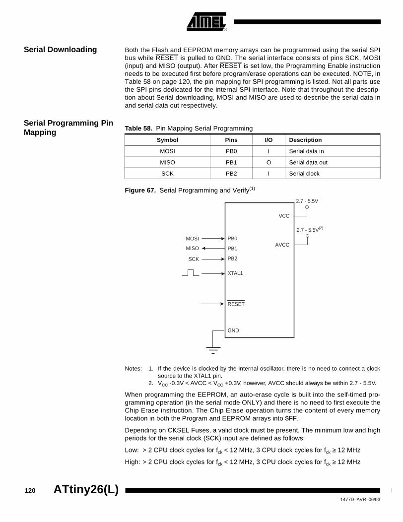
Serial Downloading Both the Flash and EEPROM memory arrays can be programmed using the serial SPIbus while RESET is pulled to GND. The serial interface consists of pins SCK, MOSI(input) and MISO (output). After RESET is set low, the Programming Enable instructionneeds to be executed first before program/erase operations can be executed. NOTE, inTable 58 on page 120, the pin mapping for SPI programming is listed. Not all parts usethe SPI pins dedicated for the internal SPI interface. Note that throughout the descrip-tion about Serial downloading, MOSI and MISO are used to describe the serial data inand serial data out respectively.
Serial Programming Pin Mapping
Figure 67. Serial Programming and Verify(1)
Notes: 1. If the device is clocked by the internal oscillator, there is no need to connect a clocksource to the XTAL1 pin.
2. VCC -0.3V < AVCC < VCC +0.3V, however, AVCC should always be within 2.7 - 5.5V.
When programming the EEPROM, an auto-erase cycle is built into the self-timed pro-gramming operation (in the serial mode ONLY) and there is no need to first execute theChip Erase instruction. The Chip Erase operation turns the content of every memorylocation in both the Program and EEPROM arrays into $FF.
Depending on CKSEL Fuses, a valid clock must be present. The minimum low and highperiods for the serial clock (SCK) input are defined as follows:
Low: > 2 CPU clock cycles for fck < 12 MHz, 3 CPU clock cycles for fck ≥ 12 MHz
High: > 2 CPU clock cycles for fck < 12 MHz, 3 CPU clock cycles for fck ≥ 12 MHz
Table 58. Pin Mapping Serial Programming
Symbol Pins I/O Description
MOSI PB0 I Serial data in
MISO PB1 O Serial data out
SCK PB2 I Serial clock
VCC
GND
XTAL1
SCK
MISO
MOSI
RESET
PB0
PB1
PB2
2.7 - 5.5V
AVCC
2.7 - 5.5V(2)
120 ATtiny26(L) 1477D–AVR–06/03
ATtiny26(L)
SPI Serial Programming Algorithm
When writing serial data to the ATtiny26, data is clocked on the rising edge of SCK.
When reading data from the ATtiny26, data is clocked on the falling edge of SCK. SeeFigure 68, Figure 69, and Table 69 for timing details.
To program and verify the ATtiny26 in the serial programming mode, the followingsequence is recommended (See four byte instruction formats in Table 60):
1. Power-up sequence:Apply power between VCC and GND while RESET and SCK are set to “0”. In some systems, the programmer can not guarantee that SCK is held low during Power-up. In this case, RESET must be given a positive pulse of at least two CPU clock cycles duration after SCK has been set to “0”.
2. Wait for at least 20 ms and enable serial programming by sending the Program-ming Enable serial instruction to pin MOSI.
3. The serial programming instructions will not work if the communication is out of synchronization. When in synchronize the second byte ($53), will echo back when issuing the third byte of the Programming Enable instruction. Whether the echo is correct or not, all 4 bytes of the instruction must be transmitted. If the $53 did not echo back, give RESET a positive pulse and issue a new Programming Enable command.
4. The Flash is programmed one page at a time. The page size is found in Table 55 on page 110. The memory page is loaded one byte at a time by supplying the 4 LSB of the address and data together with the Load Program Memory Page instruction. To ensure correct loading of the page, the data low byte must be loaded before data high byte is applied for given address. The Program Memory Page is stored by loading the Write Program Memory Page instruction with the 6 MSB of the address. If polling is not used, the user must wait at least tWD_FLASH before issuing the next page. (See Table 59). Accessing the serial programming interface before the Flash write operation completes can result in incorrect programming.
5. The EEPROM array is programmed one byte at a time by supplying the address and data together with the appropriate Write instruction. An EEPROM memory location is first automatically erased before new data is written. If polling is not used, the user must wait at least tWD_EEPROM before issuing the next byte. (See Table 59). In a chip erased device, no $FFs in the data file(s) need to be programmed.
6. Any memory location can be verified by using the Read instruction which returns the content at the selected address at serial output MISO.
7. At the end of the programming session, RESET can be set high to commence normal operation.
8. Power-off sequence (if needed):Set RESET to “1”.Turn VCC power off.
1211477D–AVR–06/03

Data Polling Flash When a page is being programmed into the Flash, reading an address location withinthe page being programmed will give the value $FF. At the time the device is ready for anew page, the programmed value will read correctly. This is used to determine when thenext page can be written. Note that the entire page is written simultaneously and anyaddress within the page can be used for polling. Data polling of the Flash will not workfor the value $FF, so when programming this value, the user will have to wait for at leasttWD_FLASH before programming the next page. As a chip-erased device contains $FF inall locations, programming of addresses that are meant to contain $FF, can be skipped.See Table 59 for tWD_FLASH value.
Data Polling EEPROM When a new byte has been written and is being programmed into EEPROM, reading theaddress location being programmed will give the value $FF. At the time the device isready for a new byte, the programmed value will read correctly. This is used to deter-mine when the next byte can be written. This will not work for the value $FF, but the usershould have the following in mind: As a chip-erased device contains $FF in all locations,programming of addresses that are meant to contain $FF, can be skipped. This doesnot apply if the EEPROM is re-programmed without chip-erasing the device. In thiscase, data polling cannot be used for the value $FF, and the user will have to wait atleast tWD_EEPROM before programming the next byte. See Table 59 for tWD_EEPROM value.
Figure 68. Serial Programming Waveforms
Table 59. Minimum Wait Delay before Writing the Next Flash or EEPROM Location
Symbol Minimum Wait Delay
tWD_FLASH 4.5 ms
tWD_EEPROM 9.0 ms
tWD_ERASE 9.0 ms
tWD_FUSE 4.5 ms
MSB
MSB
LSB
LSB
SERIAL CLOCK INPUT(SCK)
SERIAL DATA INPUT (MOSI)
(MISO)
SAMPLE
SERIAL DATA OUTPUT
122 ATtiny26(L) 1477D–AVR–06/03

ATtiny26(L)
Note: a = address high bitsb = address low bitsH = 0 – Low byte, 1 – High Byteo = data outi = data inx = don’t care
Table 60. Serial Programming Instruction Set
Instruction Instruction Format Operation
Byte 1 Byte 2 Byte 3 Byte4
Programming Enable 1010 1100 0101 0011 xxxx xxxx xxxx xxxx Enable Serial Programming after RESET goes low.
Chip Erase 1010 1100 100x xxxx xxxx xxxx xxxx xxxx Chip Erase EEPROM and Flash.
Read Program Memory 0010 H000 xxxx xxaa bbbb bbbb oooo oooo Read H (high or low) data o from Program memory at word address a:b.
Load Program Memory Page 0100 H000 xxxx xxxx xxxx bbbb iiii iiii Write H (high or low) data i to Program Memory page at word address b. Data low byte must be loaded before data high byte is applied within the same address.
Write Program Memory Page 0100 1100 xxxx xxaa bbbb xxxx xxxx xxxx Write Program Memory Page at address a:b.
Read EEPROM Memory 1010 0000 xxxx xxxx xbbb bbbb oooo oooo Read data o from EEPROM memory at address b.
Write EEPROM Memory 1100 0000 xxxx xxxx xbbb bbbb iiii iiii Write data i to EEPROM memory at address b.
Read Lock Bits 0101 1000 0000 0000 xxxx xxxx xxxx xxoo Read Lock bits. “0” = programmed, “1” = unprogrammed. See Table 47 on page 106 for details.
Write Lock Bits 1010 1100 111x xxxx xxxx xxxx 1111 11ii Write Lock bits. Set bits = “0” to program Lock bits. See Table 47 on page 106 for details.
Read Signature Byte 0011 0000 xxxx xxxx xxxx xxbb oooo oooo Read Signature Byte o at address b.
Write Fuse Bits 1010 1100 1010 0000 xxxx xxxx iiii iiii Set bits = “0” to program, “1” to unprogram. See Table 50 on page 107 for details.
Write Fuse High Bits 1010 1100 1010 1000 xxxx xxxx xxxi iiii Set bits = “0” to program, “1” to unprogram. See Table 49 on page 107 for details.
Read Fuse Bits 0101 0000 0000 0000 xxxx xxxx oooo oooo Read Fuse bits. “0” = programmed, “1” = unprogrammed. See Table 50 on page 107 for details.
Read Fuse High Bits 0101 1000 0000 1000 xxxx xxxx xxxo oooo Read Fuse high bits. “0” = programmed, “1” = unprogrammed. See Table 49 on page 107 for details.
Read Calibration Byte 0011 1000 xxxx xxxx 0000 00bb oooo oooo Read Calibration Byte o.
1231477D–AVR–06/03

Serial Programming Characteristics
Figure 69. Serial Programming Timing
Note: 1. 2 tCLCL for fck < 12 MHz, 3 tCLCL for fck >= 12 MHz
Table 61. Serial Programming Characteristics, TA = -40°C to 85°C, VCC = 2.7V - 5.5V(Unless Otherwise Noted)(1)
Symbol Parameter Min Typ Max Units
1/tCLCL Oscillator Frequency (VCC = 2.7 - 5.5 V) 0 8 MHz
tCLCL Oscillator Period (VCC = 2.7 - 5.5 V) 125 ns
1/tCLCL Oscillator Frequency (VCC = 4.5 - 5.5 V) 0 16 MHz
tCLCL Oscillator Period (VCC = 4.5 - 5.5 V) 62.5 ns
tSHSL SCK Pulse Width High 2 tCLCL(1) ns
tSLSH SCK Pulse Width Low 2 tCLCL(1) ns
tOVSH MOSI Setup to SCK High tCLCL ns
tSHOX MOSI Hold after SCK High 2 tCLCL ns
tSLIV SCK Low to MISO Valid 20 ns
MOSI
MISO
SCK
tOVSH
tSHSL
tSLSHtSHOX
tSLIV
124 ATtiny26(L) 1477D–AVR–06/03

ATtiny26(L)
Electrical Characteristics
Absolute Maximum Ratings* Operating Temperature.................................. -55°C to +125°C *NOTICE: Stresses beyond those listed under “Absolute
Maximum Ratings” may cause permanent dam-age to the device. This is a stress rating only and functional operation of the device at these or other conditions beyond those indicated in the operational sections of this specification is not implied. Exposure to absolute maximum rating conditions for extended periods may affect device reliability.
Storage Temperature ..................................... -65°C to +150°C
Voltage on Any Pin except RESETwith Respect to Ground .............................-1.0V to VCC + 0.5V
Voltage on RESET with Respect to Ground ....-1.0V to +13.0V
Maximum Operating Voltage ............................................ 6.0V
DC Current per I/O Pin ............................................... 40.0 mA
DC Current VCC and GND Pins ................................ 200.0 mA
DC Characteristics TA = -40°C to 85°C, VCC = 2.7V to 5.5V (unless otherwise noted)(1)
Symbol Parameter Condition Min. Typ. Max. Units
VIL Input Low Voltage Except XTAL1 pin -0.5 0.2VCC V
VIL1 Input Low VoltageXTAL1 pin, External Clock Selected
-0.5 0.1VCC V
VIH Input High VoltageExcept XTAL1 and RESET pins
0.6VCC(3) VCC +0.5 V
VIH1 Input High VoltageXTAL1 pin, External Clock Selected
0.8VCC(3) VCC +0.5 V
VIH2 Input High Voltage RESET pin 0.9VCC(3) VCC +0.5 V
VOLOutput Low Voltage(4)
(Ports A, B)IOL = 20 mA, VCC = 5VIOL = 10 mA, VCC = 3V
0.60.5
VV
VOHOutput High Voltage(5)
(Ports A, B)IOH = -20 mA, VCC = 5VIOH = -10 mA, VCC = 3V
4.22.3
VV
IILInput LeakageCurrent I/O Pin
Vcc = 5.5V, pin low(absolute value)
8 µA
IIHInput LeakageCurrent I/O Pin
Vcc = 5.5V, pin high(absolute value)
8 µA
RRST Reset Pull-up Resistor 20 100 kΩ
Rpu I/O Pin Pull-up Resistor 20 100 kΩ
1251477D–AVR–06/03

Notes: 1. Typical values contained in this data sheet are based on simulations and characterization of other AVR microcontrollersmanufactured on the same process technology. Min and Max values will be available after the device is characterized.
2. “Max” means the highest value where the pin is guaranteed to be read as low3. “Min” means the lowest value where the pin is guaranteed to be read as high4. Although each I/O port can sink more than the test conditions (20mA at Vcc = 5V, 10 mA at Vcc = 3V) under steady state
conditions (non-transient), the following must be observed:1] The sum of all IOL, for all ports, should not exceed 400 mA.2] The sum of all IOL, for port A0 - A7, should not exceed 300 mA.3] The sum of all IOL, for ports B0 - B7 should not exceed 300 mA.If IOL exceeds the test condition, VOL may exceed the related specification. Pins are not guaranteed to sink current greaterthan the listed test condition.
5. Although each I/O port can source more than the test conditions (20 mA at VCC = 5V, 10 mA at VCC = 3V) under steady stateconditions (non-transient), the following must be observed:1] The sum of all IOH, for all ports, should not exceed 400 mA.2] The sum of all IOH, for port A0 - A7, should not exceed 300 mA.3] The sum of all IOH, for ports B0 - B7 should not exceed 300 mA.If IOH exceeds the test condition, VOH may exceed the related specification. Pins are not guaranteed to source currentgreater than the listed test condition.
6. Minimum VCC for Power-down is 2.5V.
ICC
Power Supply Current
Active 4 MHz, VCC = 3V
(ATtiny26L)6 mA
Active 8 MHz, VCC = 5V
(ATtiny26)15 mA
Idle 4 MHz, VCC = 3V
(ATtiny26L)2 mA
Idle 8 MHz, VCC = 5V
(ATtiny26)7 mA
Power-down mode(6)WDT enabled, VCC = 3V 30 µA
WDT disabled, VCC = 3V 10 µA
VACIOAnalog Comparator Input Offset Voltage
VCC = 5V
Vin = VCC/240 mV
IACLKAnalog Comparator Input Leakage Current
VCC = 5VVin = VCC/2
-50 50 nA
tACIDAnalog Comparator Propagation Delay
VCC = 2.7VVCC = 4.0V
750500
ns
DC Characteristics TA = -40°C to 85°C, VCC = 2.7V to 5.5V (unless otherwise noted)(1) (Continued)
Symbol Parameter Condition Min. Typ. Max. Units
126 ATtiny26(L) 1477D–AVR–06/03

ATtiny26(L)
External Clock Drive Waveforms
Figure 70. External Clock Drive Waveforms
External Clock Drive
VIL1
VIH1
Table 62. External Clock Drive
Symbol Parameter
VCC = 2.7 - 5.5V VCC = 4.5 - 5.5V
UnitsMin Max Min Max
1/tCLCL Oscillator Frequency 0 8 0 16 MHz
tCLCL Clock Period 125 62.5 ns
tCHCX High Time 50 25 ns
tCLCX Low Time 50 25 ns
tCLCH Rise Time 1.6 0.5 µs
tCHCL Fall Time 1.6 0.5 µs
∆tCLCL
Change in period from one clock cycle to the next
2 2
1271477D–AVR–06/03

ADC Characteristics – Preliminary Data
Notes: 1. Values are guidelines only. Actual values are TBD.2. Minimum for AVCC is 2.7V. 3. Maximum for AVCC is 5.5V
Table 63. ADC Characteristics, Single Ended Channels
Symbol Parameter Condition Min(1) Typ(1) Max(1) Units
Resolution Single Ended Conversion 10 Bits
Absolute Accuracy
(Including INL, DNL, Quantization Error, Gain and Offset Error)
Single Ended ConversionVREF = 4V, VCC = 4VADC clock = 200 kHz
1 LSB
Single Ended ConversionVREF = 4V, VCC = 4VADC clock = 1 MHz
2 LSB
Single Ended ConversionVREF = 4V, VCC = 4VADC clock = 200 kHz
Noise Reduction mode
1 LSB
Single Ended ConversionVREF = 4V, VCC = 4VADC clock = 1 MHz
Noise Reduction mode
2 LSB
Integral Non-linearity (INL)Single Ended ConversionVREF = 4V, VCC = 4VADC clock = 200 kHz
0.5LSB
Differential Non-linearity (DNL)Single Ended ConversionVREF = 4V, VCC = 4VADC clock = 200 kHz
0.5LSB
Gain ErrorSingle Ended ConversionVREF = 4V, VCC = 4VADC clock = 200 kHz
0.75%
Offset errorSingle Ended ConversionVREF = 4V, VCC = 4VADC clock = 200 kHz
0.5LSB
Clock Frequency 50 1000 kHz
Conversion Time 13 260 µs
AVCC Analog Supply Voltage VCC - 0.3(2) VCC + 0.3(3) V
VREF Reference Voltage 2.0 AVCC V
VIN Input Voltage GND VREF V
ADC Conversion Output 0 1023 LSB
Input Bandwidth 38.5 kHz
VINT Internal Voltage Reference 2.3 2.56 2.7 V
RREF Reference Input Resistance 32 kΩ
RAIN Analog Input Resistance 100 MΩ
128 ATtiny26(L) 1477D–AVR–06/03

ATtiny26(L)
Notes: 1. Values are guidelines only. Actual values are TBD.2. Minimum for AVCC is 2.7V.3. Maximum for AVCC is 5.5V.
Table 64. ADC Characteristics, Differential Channels
Symbol Parameter Condition Min(1) Typ(1) Max(1) Units
ResolutionGain = 1x 10 Bits
Gain = 20x 10 Bits
Absolute Accuracy
Gain = 1xVREF = 4V, VCC = 5VADC clock = 50 - 200 kHz
24 LSB
Gain = 1xVREF = 4V, VCC = 5VADC clock = 50 - 200 kHz
27 LSB
Integral Non-linearity (INL)
(Accuracy after Calibration for Offset and Gain Error)
Gain = 1xVREF = 4V, VCC = 5VADC clock = 50 - 200 kHz
1 LSB
Gain = 20xVREF = 4V, VCC = 5VADC clock = 50 - 200 kHz
1.5 LSB
Gain ErrorGain = 1x 2 %
Gain = 20x 4.5 %
Offset Error
Gain = 1xVREF = 4V, VCC = 5VADC clock = 50 - 200 kHz
4 LSB
Gain = 20xVREF = 4V, VCC = 5VADC clock = 50 - 200 kHz
6 LSB
Clock Frequency 50 200 kHz
Conversion Time 26 65 µs
AVCC Analog Supply Voltage VCC - 0.3(2) VCC + 0.3(3) V
VREF Reference Voltage 2.0 AVCC - 0.5 V
VIN Input Voltage GND VCC V
VDIFF Input Differential Voltage 0 VREF/Gain V
ADC Conversion Output 0 1023 LSB
Input Bandwidth 4 kHz
VINT Internal Voltage Reference 2.3 2.56 2.7 V
RREF Reference Input Resistance 32 kΩ
RAIN Analog Input Resistance 100 MΩ
1291477D–AVR–06/03
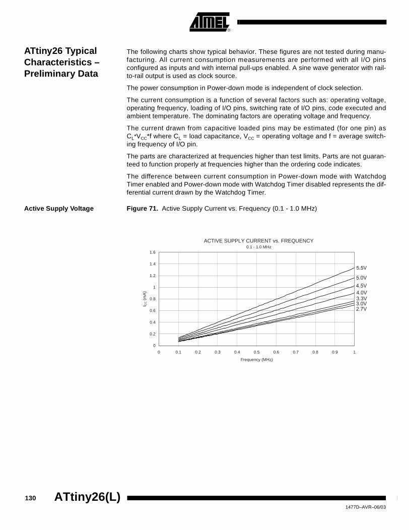
ATtiny26 Typical Characteristics – Preliminary Data
The following charts show typical behavior. These figures are not tested during manu-facturing. All current consumption measurements are performed with all I/O pinsconfigured as inputs and with internal pull-ups enabled. A sine wave generator with rail-to-rail output is used as clock source.
The power consumption in Power-down mode is independent of clock selection.
The current consumption is a function of several factors such as: operating voltage,operating frequency, loading of I/O pins, switching rate of I/O pins, code executed andambient temperature. The dominating factors are operating voltage and frequency.
The current drawn from capacitive loaded pins may be estimated (for one pin) asCL*VCC*f where CL = load capacitance, VCC = operating voltage and f = average switch-ing frequency of I/O pin.
The parts are characterized at frequencies higher than test limits. Parts are not guaran-teed to function properly at frequencies higher than the ordering code indicates.
The difference between current consumption in Power-down mode with WatchdogTimer enabled and Power-down mode with Watchdog Timer disabled represents the dif-ferential current drawn by the Watchdog Timer.
Active Supply Voltage Figure 71. Active Supply Current vs. Frequency (0.1 - 1.0 MHz)
ACTIVE SUPPLY CURRENT vs. FREQUENCY0.1 - 1.0 MHz
0
0.2
0.4
0.6
0.8
1
1.2
1.4
1.6
0 0.1 0.2 0.3 0.4 0.5 0.6 0.7 0.8 0.9 1
Frequency (MHz)
I CC (
mA
)
5.5V
4.5V
4.0V3.3V
2.7V3.0V
5.0V
130 ATtiny26(L) 1477D–AVR–06/03
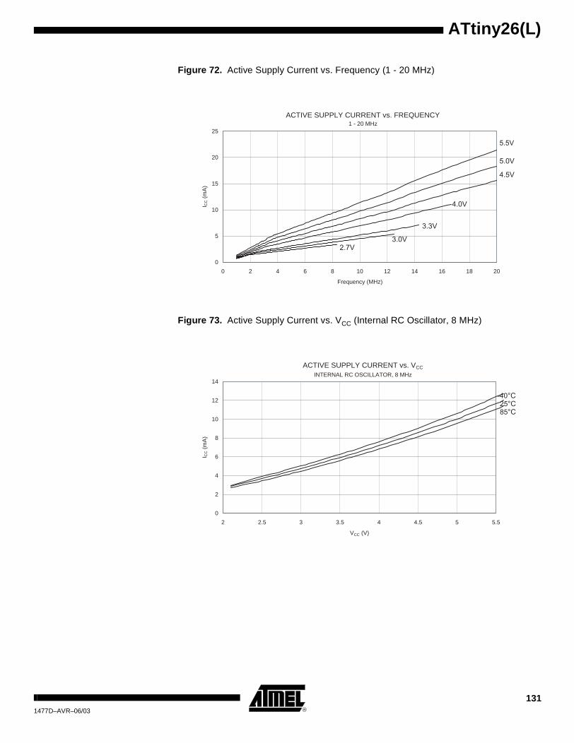
ATtiny26(L)
Figure 72. Active Supply Current vs. Frequency (1 - 20 MHz)
Figure 73. Active Supply Current vs. VCC (Internal RC Oscillator, 8 MHz)
ACTIVE SUPPLY CURRENT vs. FREQUENCY1 - 20 MHz
0
5
10
15
20
25
0 2 4 6 8 10 12 14 16 18 20
Frequency (MHz)
I CC (
mA
)
5.5V
4.5V
4.0V
3.3V
2.7V3.0V
5.0V
ACTIVE SUPPLY CURRENT vs. VCC
INTERNAL RC OSCILLATOR, 8 MHz
0
2
4
6
8
10
12
14
2 2.5 3 3.5 4 4.5 5 5.5
VCC (V)
I CC (
mA
)
85°C25°C
-40°C
1311477D–AVR–06/03

Figure 74. Active Supply Current vs. VCC (Internal RC Oscillator, 4 MHz)
Figure 75. Active Supply Current vs. VCC (Internal RC Oscillator, 2 MHz)
ACTIVE SUPPLY CURRENT vs. VCC
INTERNAL RC OSCILLATOR, 4 MHz
0
1
2
3
4
5
6
7
8
2 2.5 3 3.5 4 4.5 5 5.5
VCC (V)
I CC (
mA
)
85°C
25°C-40°C
ACTIVE SUPPLY CURRENT vs. VCC
INTERNAL RC OSCILLATOR, 2 MHz
0
0.5
1
1.5
2
2.5
3
3.5
4
2 2.5 3 3.5 4 4.5 5 5.5
VCC (V)
I CC (
mA
)
85°C25°C
-40°C
132 ATtiny26(L) 1477D–AVR–06/03

ATtiny26(L)
Figure 76. Active Supply Current vs. VCC (Internal RC Oscillator, 1 MHz)
Figure 77. Active Supply Current vs. VCC (PLL Oscillator)
ACTIVE SUPPLY CURRENT vs. VCC
INTERNAL RC OSCILLATOR, 1 MHz
0
0.2
0.4
0.6
0.8
1
1.2
1.4
1.6
1.8
2 2.5 3 3.5 4 4.5 5 5.5
VCC (V)
I CC (
mA
)
85°C
25°C
-40°C
ACTIVE SUPPLY CURRENT vs. VCC
PLL OSCILLATOR
0
5
10
15
20
25
2 2.5 3 3.5 4 4.5 5 5.5
VCC (V)
I CC (
mA
)
85°C25°C
-40°C
1331477D–AVR–06/03

Figure 78. Active Supply Current vs. VCC (32 kHz External Oscillator)
Idle Supply Current Figure 79. Idle Supply Current vs. Frequency (0.1 - 1.0 MHz)
ACTIVE SUPPLY CURRENT vs. VCC
32kHz EXTERNAL OSCILLATOR
0
10
20
30
40
50
60
70
1.5 2 2.5 3 3.5 4 4.5 5 5.5
VCC (V)
I CC (
uA)
25°C
IDLE SUPPLY CURRENT vs. FREQUENCY0.1 - 1.0 MHz
0
0.1
0.2
0.3
0.4
0.5
0.6
0 0.1 0.2 0.3 0.4 0.5 0.6 0.7 0.8 0.9 1
Frequency (MHz)
I CC (
mA
)
5.5V
4.5V
4.0V
3.3V
2.7V3.0V
5.0V
134 ATtiny26(L) 1477D–AVR–06/03

ATtiny26(L)
Figure 80. Idle Supply Current vs. Frequency (1 - 20 MHz)
Figure 81. Idle Supply Current vs. VCC (Internal RC Oscillator, 8 MHz)
IDLE SUPPLY CURRENT vs. FREQUENCY1 - 20 MHz
0
2
4
6
8
10
12
0 2 4 6 8 10 12 14 16 18 20
Frequency (MHz)
I CC (
mA
)
5.5V
4.5V
4.0V
3.3V
2.7V3.0V
5.0V
IDLE SUPPLY CURRENT vs. VCC
INTERNAL RC OSCILLATOR, 8 MHz
0
1
2
3
4
5
6
7
2 2.5 3 3.5 4 4.5 5 5.5
VCC (V)
I CC (
mA
)
85°C25°C
-40°C
1351477D–AVR–06/03

Figure 82. Idle Supply Current vs. VCC (Internal RC Oscillator, 4 MHz)
Figure 83. Idle Supply Current vs. VCC (Internal RC Oscillator, 2 MHz)
IDLE SUPPLY CURRENT vs. VCC
INTERNAL RC OSCILLATOR, 4 MHz
0
0.5
1
1.5
2
2.5
3
3.5
2 2.5 3 3.5 4 4.5 5 5.5
VCC (V)
I CC (
mA
)
85°C25°C
-40°C
IDLE SUPPLY CURRENT vs. VCC
INTERNAL RC OSCILLATOR, 2 MHz
0
0.2
0.4
0.6
0.8
1
1.2
1.4
1.6
2 2.5 3 3.5 4 4.5 5 5.5
VCC (V)
I CC (
mA
)
85°C
25°C
-40°C
136 ATtiny26(L) 1477D–AVR–06/03

ATtiny26(L)
Figure 84. Idle Supply Current vs. VCC (Internal RC Oscillator, 1 MHz)
Figure 85. Idle Supply Current vs. VCC (PLL Oscillator)
IDLE SUPPLY CURRENT vs. VCC
INTERNAL RC OSCILLATOR, 1 MHz
0
0.1
0.2
0.3
0.4
0.5
0.6
0.7
0.8
2 2.5 3 3.5 4 4.5 5 5.5
VCC (V)
I CC (
mA
)
85°C
25°C
-40°C
IDLE SUPPLY CURRENT vs. VCC
PLL OSCILLATOR
0
2
4
6
8
10
2 2.5 3 3.5 4 4.5 5 5.5
VCC (V)
I CC (
mA
)
85°C
25°C
-40°C
1371477D–AVR–06/03

Figure 86. Idle Supply Current vs. VCC (32 kHz External Oscillator)
Power-down Supply Current Figure 87. Power-down Supply Current vs. VCC (Watchdog Timer Disabled)
IDLE SUPPLY CURRENT vs. VCC
32kHz EXTERNAL OSCILLATOR
0
5
10
15
20
25
30
2 2.5 3 3.5 4 4.5 5 5.5
VCC (V)
I CC (
uA)
25°C
POWER-DOWN SUPPLY CURRENT vs. VCC
WATCHDOG TIMER DISABLED
0
0.2
0.4
0.6
0.8
1
1.2
1.4
1.6
1.8
2 2.5 3 3.5 4 4.5 5 5.5
VCC (V)
I CC (
uA)
85°C
25°C
-40°C
138 ATtiny26(L) 1477D–AVR–06/03

ATtiny26(L)
Figure 88. Power-down Supply Current vs. VCC (Watchdog Timer Enabled)
Standby Supply Current Figure 89. Standby Supply Current vs. VCC (455 kHz Resonator, Watchdog TimerDisabled)
POWER-DOWN SUPPLY CURRENT vs. VCC
WATCHDOG TIMER ENABLED
0
2
4
6
8
10
12
14
16
18
20
2 2.5 3 3.5 4 4.5 5 5.5
VCC (V)
I CC (
uA)
85°C25°C
-40°C
STANDBY SUPPLY CURRENT vs. VCC
455 kHz RESONATOR, WATCHDOG TIMER DISABLED
0
10
20
30
40
50
60
70
2 2.5 3 3.5 4 4.5 5 5.5
VCC (V)
I CC (
uA)
1391477D–AVR–06/03
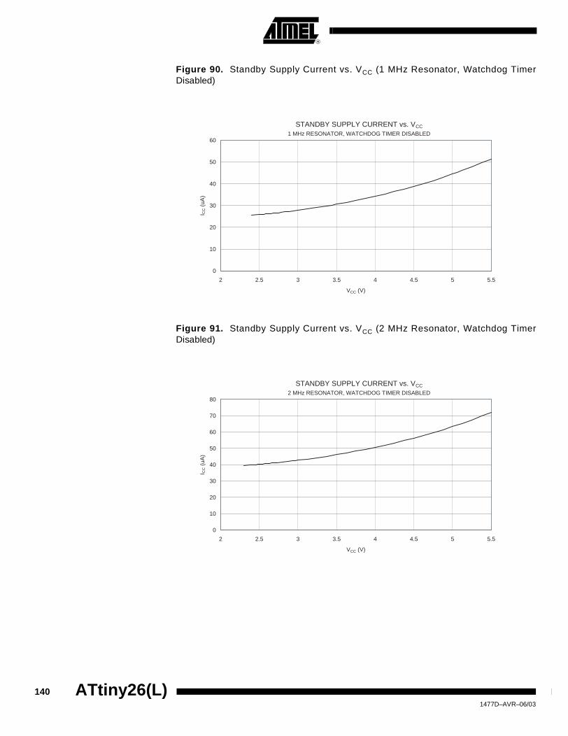
Figure 90. Standby Supply Current vs. VCC (1 MHz Resonator, Watchdog TimerDisabled)
Figure 91. Standby Supply Current vs. VCC (2 MHz Resonator, Watchdog TimerDisabled)
STANDBY SUPPLY CURRENT vs. VCC
1 MHz RESONATOR, WATCHDOG TIMER DISABLED
0
10
20
30
40
50
60
2 2.5 3 3.5 4 4.5 5 5.5
VCC (V)
I CC (
uA)
STANDBY SUPPLY CURRENT vs. VCC
2 MHz RESONATOR, WATCHDOG TIMER DISABLED
0
10
20
30
40
50
60
70
80
2 2.5 3 3.5 4 4.5 5 5.5
VCC (V)
I CC (
uA)
140 ATtiny26(L) 1477D–AVR–06/03

ATtiny26(L)
Figure 92. Standby Supply Current vs. VCC (2 MHz XTAL, Watchdog Timer Disabled)
Figure 93. Standby Supply Current vs. VCC (4 MHz Resonator, Watchdog TimerDisabled)
STANDBY SUPPLY CURRENT vs. VCC
2 MHz XTAL, WATCHDOG TIMER DISABLED
0
10
20
30
40
50
60
70
80
90
2 2.5 3 3.5 4 4.5 5 5.5
VCC (V)
I CC (
uA)
STANDBY SUPPLY CURRENT vs. VCC
4 MHz RESONATOR, WATCHDOG TIMER DISABLED
0
20
40
60
80
100
120
2 2.5 3 3.5 4 4.5 5 5.5
VCC (V)
I CC (
uA)
1411477D–AVR–06/03
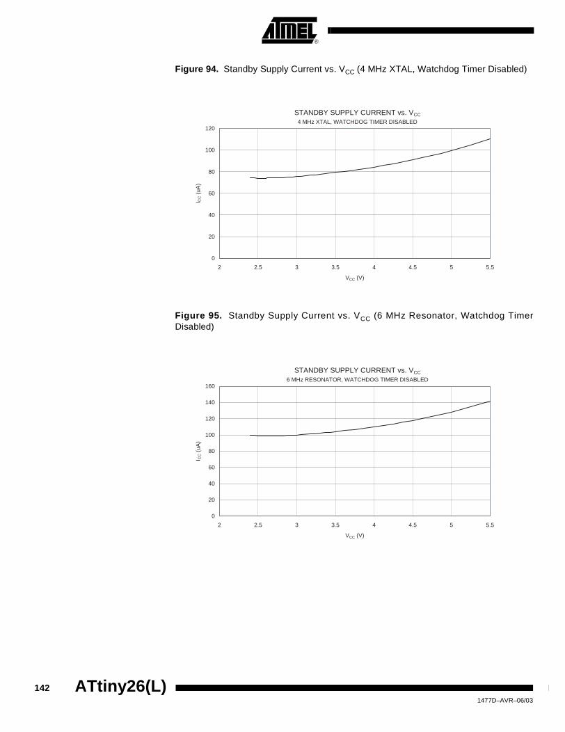
Figure 94. Standby Supply Current vs. VCC (4 MHz XTAL, Watchdog Timer Disabled)
Figure 95. Standby Supply Current vs. VCC (6 MHz Resonator, Watchdog TimerDisabled)
STANDBY SUPPLY CURRENT vs. VCC
4 MHz XTAL, WATCHDOG TIMER DISABLED
0
20
40
60
80
100
120
2 2.5 3 3.5 4 4.5 5 5.5
VCC (V)
I CC (
uA)
STANDBY SUPPLY CURRENT vs. VCC
6 MHz RESONATOR, WATCHDOG TIMER DISABLED
0
20
40
60
80
100
120
140
160
2 2.5 3 3.5 4 4.5 5 5.5
VCC (V)
I CC (
uA)
142 ATtiny26(L) 1477D–AVR–06/03

ATtiny26(L)
Figure 96. Standby Supply Current vs. VCC (6 MHz XTAL, Watchdog Timer Disabled)
Pin Pull-up Figure 97. I/O Pin Pull-up Resistor Current vs. Input Voltage (VCC = 5V)
STANDBY SUPPLY CURRENT vs. VCC
6 MHz XTAL, WATCHDOG TIMER DISABLED
0
20
40
60
80
100
120
140
160
180
2 2.5 3 3.5 4 4.5 5 5.5
VCC (V)
I CC (
uA)
I/O PIN PULL-UP RESISTOR CURRENT vs. INPUT VOLTAGEVcc = 5V
0
20
40
60
80
100
120
140
160
0 1 2 3 4 5 6
VOP (V)
I OP (
uA)
85°C
25°C
-40°C
1431477D–AVR–06/03

Figure 98. I/O Pin Pull-up Resistor Current vs. Input Voltage (VCC = 2.7V)
Figure 99. Reset Pull-up Resistor Current vs. Reset Pin Voltage (VCC = 5V)
I/O PIN PULL-UP RESISTOR CURRENT vs. INPUT VOLTAGEVcc = 2.7V
0
10
20
30
40
50
60
70
80
0 0.5 1 1.5 2 2.5 3
VOP (V)
I OP (
uA)
85°C25°C
-40°C
RESET PULL-UP RESISTOR CURRENT vs. RESET PIN VOLTAGEVcc = 5V
0
20
40
60
80
100
120
VRESET (V)
I RE
SE
T (
uA)
-40°C 25°C
85°C
144 ATtiny26(L) 1477D–AVR–06/03
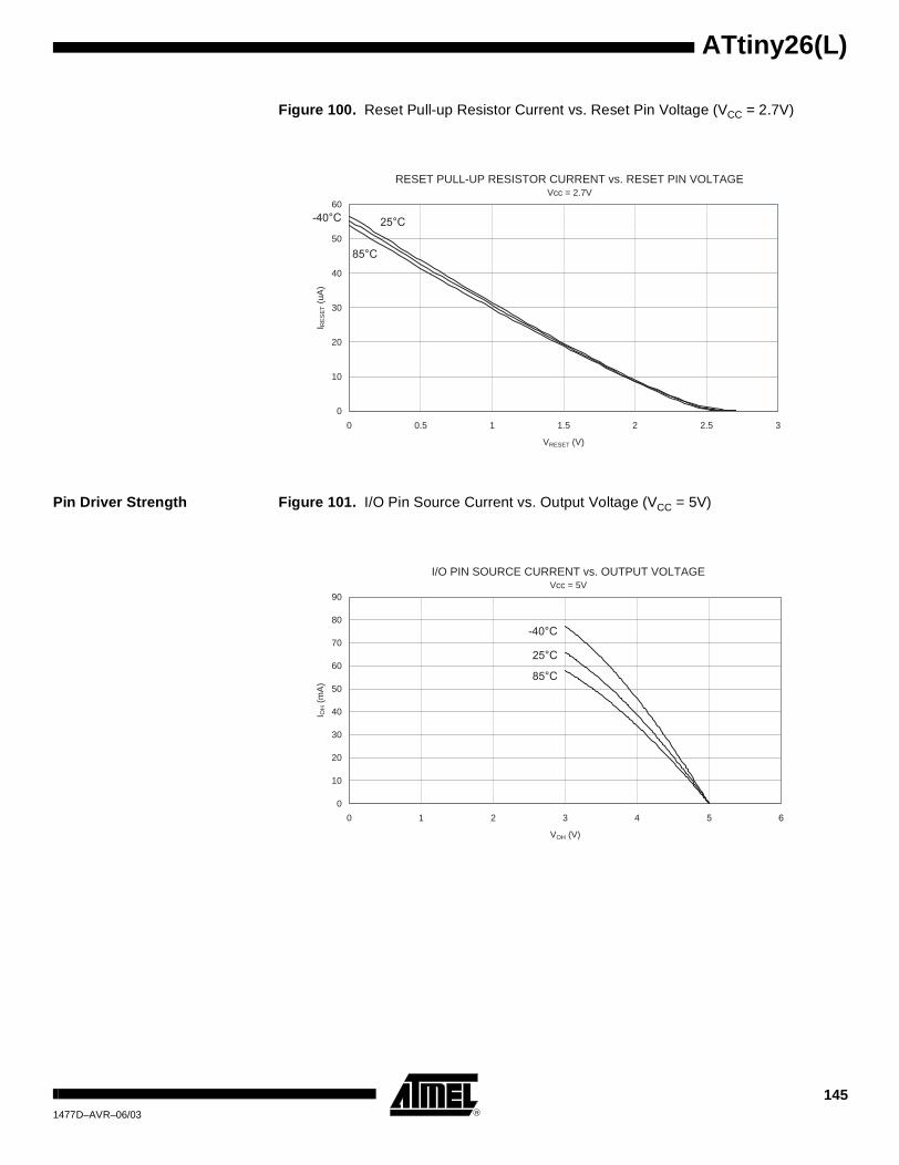
ATtiny26(L)
Figure 100. Reset Pull-up Resistor Current vs. Reset Pin Voltage (VCC = 2.7V)
Pin Driver Strength Figure 101. I/O Pin Source Current vs. Output Voltage (VCC = 5V)
RESET PULL-UP RESISTOR CURRENT vs. RESET PIN VOLTAGEVcc = 2.7V
0
10
20
30
40
50
60
0 0.5 1 1.5 2 2.5 3
VRESET (V)
I RE
SE
T (
uA)
-40°C 25°C
85°C
I/O PIN SOURCE CURRENT vs. OUTPUT VOLTAGEVcc = 5V
0
10
20
30
40
50
60
70
80
90
0 1 2 3 4
VOH (V)
I OH (
mA
)
85°C
25°C
-40°C
1451477D–AVR–06/03

Figure 102. I/O Pin Source Current vs. Output Voltage (VCC = 2.7V)
Figure 103. I/O Pin Sink Current vs. Output Voltage (VCC = 5V)
I/O PIN SOURCE CURRENT vs. OUTPUT VOLTAGEVcc = 2.7V
0
5
10
15
20
25
30
0 0.5 1 1.5 2 2.5 3
VOH (V)
I OH (
mA
)
85°C
25°C
-40°C
I/O PIN SINK CURRENT vs. OUTPUT VOLTAGEVcc = 5V
0
10
20
30
40
50
60
70
80
90
0 0.5 1 1.5 2 2.5
VOL (V)
I OL
(mA
)
85°C
25°C
-40°C
146 ATtiny26(L) 1477D–AVR–06/03

ATtiny26(L)
Figure 104. I/O Pin Sink Current vs. Output Voltage (VCC = 2.7V)
Figure 105. Reset Pin as I/O – Source Current vs. Output Voltage (VCC = 5V)
I/O PIN SINK CURRENT vs. OUTPUT VOLTAGEVcc = 2.7V
0
5
10
15
20
25
30
35
0 0.5 1 1.5 2 2.5
VOL (V)
I OL
(mA
)
85°C
25°C
-40°C
RESET PIN AS I/O - SOURCE CURRENT vs. OUTPUT VOLTAGEVcc = 5V
0
0.2
0.4
0.6
0.8
1
1.2
1.4
0 1 2 3
VOH (V)
Cur
rent
(m
A) 85°C
25°C
-40°C
1471477D–AVR–06/03

Figure 106. Reset Pin as I/O –Sink Current vs. Output Voltage (VCC = 5V)
Figure 107. Reset Pin as I/O – Sink Current vs. Output Voltage (VCC = 2.7V)
RESET PIN AS I/O - SINK CURRENT vs. OUTPUT VOLTAGEVcc = 5V
0
2
4
6
8
10
12
14
0 0.5 1 1.5 2 2.5
VOL (V)
Cur
rent
(m
A)
85°C
25°C
-40°C
RESET PIN AS I/O - SINK CURRENT vs. OUTPUT VOLTAGEVcc = 2.7V
0
0.5
1
1.5
2
2.5
3
3.5
4
4.5
0 0.5 1 1.5 2 2.5
VOL (V)
Cur
rent
(m
A) 85°C
25°C
-40°C
148 ATtiny26(L) 1477D–AVR–06/03
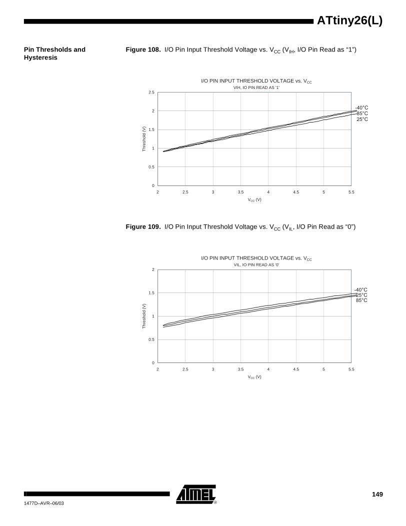
ATtiny26(L)
Pin Thresholds and Hysteresis
Figure 108. I/O Pin Input Threshold Voltage vs. VCC (VIH, I/O Pin Read as “1”)
Figure 109. I/O Pin Input Threshold Voltage vs. VCC (VIL, I/O Pin Read as “0”)
I/O PIN INPUT THRESHOLD VOLTAGE vs. VCC
VIH, IO PIN READ AS '1'
0
0.5
1
1.5
2
2.5
2 2.5 3 3.5 4 4.5 5 5.5
VCC (V)
Thr
esho
ld (
V)
85°C25°C
-40°C
I/O PIN INPUT THRESHOLD VOLTAGE vs. VCC
VIL, IO PIN READ AS '0'
0
0.5
1
1.5
2
2 2.5 3 3.5 4 4.5 5 5.5
VCC (V)
Thr
esho
ld (
V)
85°C25°C
-40°C
1491477D–AVR–06/03

Figure 110. I/O Pin Input Hysteresis vs. VCC
Figure 111. Reset Pin as I/O – Input Threshold Voltage vs. VCC (VIH, Reset Pin Read as “1”)
I/O PIN INPUT HYSTERESIS vs. VCC
0
0.1
0.2
0.3
0.4
0.5
0.6
0.7
2 2.5 3 3.5 4 4.5 5 5.5
VCC (V)
Thr
esho
ld (
V)
85°C25°C
-40°C
RESET PIN AS I/O - INPUT THRESHOLD VOLTAGE vs. VCC
VIH, RESET PIN READ AS '1'
0
0.5
1
1.5
2
2.5
2 2.5 3 3.5 4 4.5 5 5.5
VCC (V)
Thr
esho
ld (
V)
85°C25°C
-40°C
150 ATtiny26(L) 1477D–AVR–06/03

ATtiny26(L)
Figure 112. Reset Pin as I/O – Input Threshold Voltage vs. VCC (VIL, Reset Pin Read as “0”)
Figure 113. Reset Pin as I/O – Pin Hysteresis vs. VCC
RESET PIN AS I/O - INPUT THRESHOLD VOLTAGE vs. VCC
VIL, RESET PIN READ AS '0'
0
0.5
1
1.5
2
2.5
2 2.5 3 3.5 4 4.5 5 5.5
VCC (V)
Thr
esho
ld (
V)
85°C25°C
-40°C
RESET PIN AS I/O - PIN HYSTERESIS vs. VCC
0
0.1
0.2
0.3
0.4
0.5
0.6
0.7
2 2.5 3 3.5 4 4.5 5 5.5
VCC (V)
Thr
esho
ld (
V)
85°C
25°C
-40°C
1511477D–AVR–06/03

Figure 114. Reset Input Threshold Voltage vs. VCC (VIH, Reset Pin Read as “1”)
Figure 115. Reset Input Threshold Voltage vs. VCC (VIL, Reset Pin Read as “0”)
RESET INPUT THRESHOLD VOLTAGE vs. VCC
VIH, RESET PIN READ AS '1'
0
0.5
1
1.5
2
2.5
1.5 2 2.5 3 3.5 4 4.5 5 5.5
VCC (V)
Thr
esho
ld (
V)
85°C
25°C
-40°C
RESET INPUT THRESHOLD VOLTAGE vs. VCC
VIL, RESET PIN READ AS '0'
0
0.5
1
1.5
2
2.5
2 2.5 3 3.5 4 4.5 5 5.5
VCC (V)
Thr
esho
ld (
V)
85°C25°C
-40°C
152 ATtiny26(L) 1477D–AVR–06/03

ATtiny26(L)
Figure 116. Reset Input Pin Hysteresis vs. VCC
BOD Thresholds and Analog Comparator Offset
Figure 117. BOD Thresholds vs. Temperature (BOD Level is 4.3V)
RESET INPUT PIN HYSTERESIS vs. VCC
RESET PIN READ AS "0"
0
0.05
0.1
0.15
0.2
0.25
0.3
0.35
0.4
0.45
0.5
2 2.5 3 3.5 4 4.5 5 5.5 6
VCC (V)
Thr
esho
ld (
V)
85°C
25°C
-40°C
BOD THRESHOLDS vs. TEMPERATUREBODLEVEL IS 4.3V
3.8
3.9
4
4.1
4.2
4.3
-50 -40 -30 -20 -10 0 10 20 30 40 50 60 70 80 90 100
Temperature (C)
Thr
esho
ld (
V)
Rising VCC
Falling VCC
1531477D–AVR–06/03
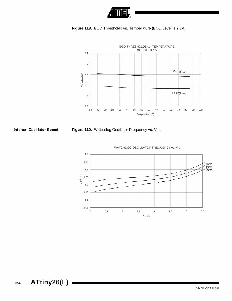
Figure 118. BOD Thresholds vs. Temperature (BOD Level is 2.7V)
Internal Oscillator Speed Figure 119. Watchdog Oscillator Frequency vs. VCC
BOD THRESHOLDS vs. TEMPERATUREBODLEVEL IS 2.7V
2.6
2.7
2.8
2.9
3
3.1
-50 -40 -30 -20 -10 0 10 20 30 40 50 60 70 80 90 100
Temperature (C)
Thr
esho
ld (
V) Rising VCC
Falling VCC
WATCHDOG OSCILLATOR FREQUENCY vs. VCC
1.05
1.1
1.15
1.2
1.25
1.3
1.35
1.4
2 2.5 3 3.5 4 4.5 5 5.5
VCC (V)
FR
C (
MH
z)
85°C25°C
-40°C
154 ATtiny26(L) 1477D–AVR–06/03

ATtiny26(L)
Figure 120. Calibrated 8 MHz RC Oscillator Frequency vs. Temperature
Figure 121. Calibrated 8 MHz RC Oscillator Frequency vs. VCC
CALIBRATED 8MHz RC OSCILLATOR FREQUENCY vs. TEMPERATURE
6.4
6.9
7.4
7.9
8.4
8.9
-60 -40 -20 0 20 40 60 80 100
Ta (˚C)
FR
C (
MH
z)5.0V
3.5V
2.7V
CALIBRATED 8MHz RC OSCILLATOR FREQUENCY vs. VCC
6
6.5
7
7.5
8
8.5
9
2 2.5 3 3.5 4 4.5 5 5.5
VCC (V)
FR
C (
MH
z) 85°C
25°C
-40°C
1551477D–AVR–06/03

Figure 122. Calibrated 8 MHz RC Oscillator Frequency vs. Osccal Value
Figure 123. Calibrated 4 MHz RC Oscillator Frequency vs. Temperature
CALIBRATED 8MHz RC OSCILLATOR FREQUENCY vs. OSCCAL VALUE
3.5
5.5
7.5
9.5
11.5
13.5
15.5
17.5
0 16 32 48 64 80 96 112 128 144 160 176 192 208 224 240
OSCCAL VALUE
FR
C (
MH
z)
CALIBRATED 4MHz RC OSCILLATOR FREQUENCY vs. TEMPERATURE
3.4
3.5
3.6
3.7
3.8
3.9
4
4.1
4.2
4.3
-60 -40 -20 0 20 40 60 80 100
Ta (˚C)
FR
C (
MH
z)
5.0V
3.5V
2.7V
156 ATtiny26(L) 1477D–AVR–06/03

ATtiny26(L)
Figure 124. Calibrated 4 MHz RC Oscillator Frequency vs. VCC
Figure 125. Calibrated 4 MHz RC Oscillator Frequency vs. Osccal Value
CALIBRATED 4MHz RC OSCILLATOR FREQUENCY vs. VCC
3.4
3.5
3.6
3.7
3.8
3.9
4
4.1
4.2
4.3
4.4
2 2.5 3 3.5 4 4.5 5 5.5
VCC (V)
FR
C (
MH
z)
85°C
25°C
-40°C
CALIBRATED 4MHz RC OSCILLATOR FREQUENCY vs. OSCCAL VALUE
1.6
2.6
3.6
4.6
5.6
6.6
7.6
8.6
9.6
0 16 32 48 64 80 96 112 128 144 160 176 192 208 224 240
OSCCAL VALUE
FR
C (
MH
z)
1571477D–AVR–06/03

Figure 126. Calibrated 2 MHz RC Oscillator Frequency vs. Temperature
Figure 127. Calibrated 2 MHz RC Oscillator Frequency vs. VCC
CALIBRATED 2MHz RC OSCILLATOR FREQUENCY vs. TEMPERATURE
1.75
1.8
1.85
1.9
1.95
2
2.05
2.1
2.15
-60 -40 -20 0 20 40 60 80 100
Ta (˚C)
FR
C (
MH
z)5.0V
3.5V
2.7V
CALIBRATED 2MHz RC OSCILLATOR FREQUENCY vs. VCC
1.7
1.75
1.8
1.85
1.9
1.95
2
2.05
2.1
2.15
2 2.5 3 3.5 4 4.5 5 5.5
VCC (V)
FR
C (
MH
z)
85°C
25°C
-40°C
158 ATtiny26(L) 1477D–AVR–06/03

ATtiny26(L)
Figure 128. Calibrated 2 MHz RC Oscillator Frequency vs. Osccal Value
Figure 129. Calibrated 1 MHz RC Oscillator Frequency vs. Temperature
CALIBRATED 2MHz RC OSCILLATOR FREQUENCY vs. OSCCAL VALUE
0.8
1.3
1.8
2.3
2.8
3.3
3.8
4.3
0 16 32 48 64 80 96 112 128 144 160 176 192 208 224 240
OSCCAL VALUE
FR
C (
MH
z)
CALIBRATED 1 MHz RC OSCILLATOR FREQUENCY vs. TEMPERATURE
0.9
0.92
0.94
0.96
0.98
1
1.02
1.04
-60 -40 -20 0 20 40 60 80 100
VCC (V)
FR
C (
MH
z)
5.0V
3.5V
2.7V
1591477D–AVR–06/03

Figure 130. Calibrated 1 MHz RC Oscillator Frequency vs. VCC
Figure 131. Calibrated 1 MHz RC Oscillator Frequency vs. Osccal Value
CALIBRATED 1MHz RC OSCILLATOR FREQUENCY vs. VCC
0.85
0.9
0.95
1
1.05
1.1
2 2.5 3 3.5 4 4.5 5 5.5
VCC (V)
FR
C (
MH
z) 85°C
25°C
-40°C
CALIBRATED 1MHz RC OSCILLATOR FREQUENCY vs. OSCCAL VALUE
0.4
0.6
0.8
1
1.2
1.4
1.6
1.8
2
0 16 32 48 64 80 96 112 128 144 160 176 192 208 224 240
OSCCAL VALUE
FR
C (
MH
z)
160 ATtiny26(L) 1477D–AVR–06/03
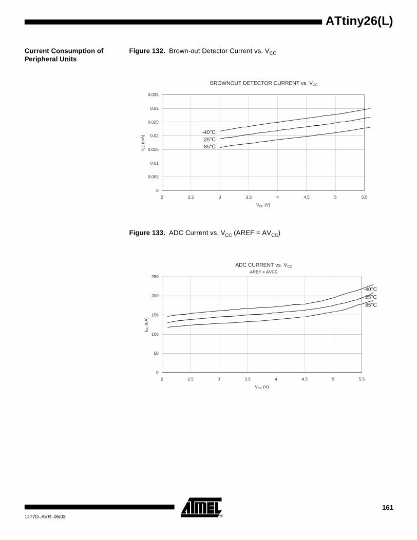
ATtiny26(L)
Current Consumption of Peripheral Units
Figure 132. Brown-out Detector Current vs. VCC
Figure 133. ADC Current vs. VCC (AREF = AVCC)
BROWNOUT DETECTOR CURRENT vs. VCC
0
0.005
0.01
0.015
0.02
0.025
0.03
0.035
2 2.5 3 3.5 4 4.5 5 5.5
VCC (V)
I CC (
mA
)25°C
85°C
-40°C
ADC CURRENT vs. VCC
AREF = AVCC
0
50
100
150
200
250
2 2.5 3 3.5 4 4.5 5 5.5
VCC (V)
I CC (
uA)
85°C
25°C
-40°C
1611477D–AVR–06/03

Figure 134. AREF External Reference Current vs. VCC
Figure 135. Analog Comparator Current vs. VCC
AREF EXTERNAL REFERENCE CURRENT vs. VCC
0
50
100
150
200
250
2 2.5 3 3.5 4 4.5 5 5.5
VCC (V)
I CC (
uA)
85°C25°C
-40°C
ANALOG COMPARATOR CURRENT vs. VCC
0
20
40
60
80
100
120
2 2.5 3 3.5 4 4.5 5 5.5
VCC (V)
I CC (
uA)
85°C
25°C
-40°C
162 ATtiny26(L) 1477D–AVR–06/03

ATtiny26(L)
Figure 136. Programming Current vs. VCC
Current Consumption in Reset and Reset Pulsewidth
Figure 137. Reset Supply Current vs. VCC (0.1 - 1.0 MHz, Excluding Current Through The Reset Pull-up)
PROGRAMMING CURRENT vs. VCC
0
1
2
3
4
5
2 2.5 3 3.5 4 4.5 5 5.5
VCC (V)
I CC (
mA
)85°C
25°C
-40°C
RESET SUPPLY CURRENT vs. VCC
0.1 - 1.0 MHz, EXCLUDING CURRENT THROUGH THE RESET PULLUP
0
0.5
1
1.5
2
2.5
3
3.5
0 0.1 0.2 0.3 0.4 0.5 0.6 0.7 0.8 0.9 1
Frequency (MHz)
I CC (
mA
)
5.5V
4.5V
4.0V
3.3V
2.7V3.0V
5.0V
1631477D–AVR–06/03

Figure 138. Reset Supply Current vs. VCC (1 - 20 MHz, Excluding Current Through The Reset Pull-up)
Figure 139. Reset Pulsewidth vs. VCC
RESET SUPPLY CURRENT vs. VCC
1 - 20 MHz, EXCLUDING CURRENT THROUGH THE RESET PULLUP
0
2
4
6
8
10
12
14
16
18
20
0 2 4 6 8 10 12 14 16 18 20
Frequency (MHz)
I CC (
mA
)
5.5V
4.5V
4.0V
3.3V
2.7V3.0V
5.0V
RESET PULSE WIDTH vs. VCC
0
200
400
600
800
1000
1200
0 1 2 3
VCC (V)
Pul
sew
idth
(ns
)
85°C
25°C
-40°C
164 ATtiny26(L) 1477D–AVR–06/03
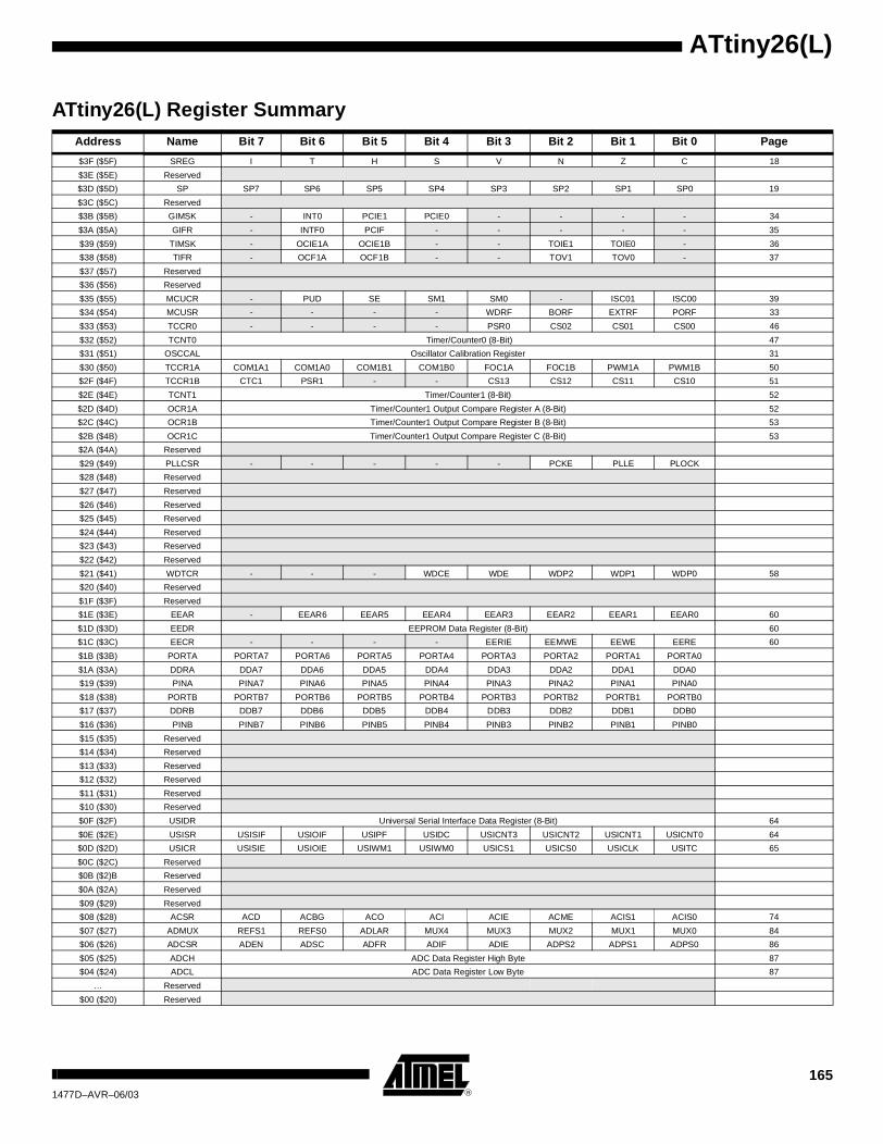
ATtiny26(L)
ATtiny26(L) Register SummaryAddress Name Bit 7 Bit 6 Bit 5 Bit 4 Bit 3 Bit 2 Bit 1 Bit 0 Page
$3F ($5F) SREG I T H S V N Z C 18
$3E ($5E) Reserved
$3D ($5D) SP SP7 SP6 SP5 SP4 SP3 SP2 SP1 SP0 19
$3C ($5C) Reserved
$3B ($5B) GIMSK - INT0 PCIE1 PCIE0 - - - - 34
$3A ($5A) GIFR - INTF0 PCIF - - - - - 35
$39 ($59) TIMSK - OCIE1A OCIE1B - - TOIE1 TOIE0 - 36
$38 ($58) TIFR - OCF1A OCF1B - - TOV1 TOV0 - 37
$37 ($57) Reserved
$36 ($56) Reserved
$35 ($55) MCUCR - PUD SE SM1 SM0 - ISC01 ISC00 39
$34 ($54) MCUSR - - - - WDRF BORF EXTRF PORF 33
$33 ($53) TCCR0 - - - - PSR0 CS02 CS01 CS00 46
$32 ($52) TCNT0 Timer/Counter0 (8-Bit) 47
$31 ($51) OSCCAL Oscillator Calibration Register 31
$30 ($50) TCCR1A COM1A1 COM1A0 COM1B1 COM1B0 FOC1A FOC1B PWM1A PWM1B 50
$2F ($4F) TCCR1B CTC1 PSR1 - - CS13 CS12 CS11 CS10 51
$2E ($4E) TCNT1 Timer/Counter1 (8-Bit) 52
$2D ($4D) OCR1A Timer/Counter1 Output Compare Register A (8-Bit) 52
$2C ($4C) OCR1B Timer/Counter1 Output Compare Register B (8-Bit) 53
$2B ($4B) OCR1C Timer/Counter1 Output Compare Register C (8-Bit) 53
$2A ($4A) Reserved
$29 ($49) PLLCSR - - - - - PCKE PLLE PLOCK
$28 ($48) Reserved
$27 ($47) Reserved
$26 ($46) Reserved
$25 ($45) Reserved
$24 ($44) Reserved
$23 ($43) Reserved
$22 ($42) Reserved
$21 ($41) WDTCR - - - WDCE WDE WDP2 WDP1 WDP0 58
$20 ($40) Reserved
$1F ($3F) Reserved
$1E ($3E) EEAR - EEAR6 EEAR5 EEAR4 EEAR3 EEAR2 EEAR1 EEAR0 60
$1D ($3D) EEDR EEPROM Data Register (8-Bit) 60
$1C ($3C) EECR - - - - EERIE EEMWE EEWE EERE 60
$1B ($3B) PORTA PORTA7 PORTA6 PORTA5 PORTA4 PORTA3 PORTA2 PORTA1 PORTA0
$1A ($3A) DDRA DDA7 DDA6 DDA5 DDA4 DDA3 DDA2 DDA1 DDA0
$19 ($39) PINA PINA7 PINA6 PINA5 PINA4 PINA3 PINA2 PINA1 PINA0
$18 ($38) PORTB PORTB7 PORTB6 PORTB5 PORTB4 PORTB3 PORTB2 PORTB1 PORTB0
$17 ($37) DDRB DDB7 DDB6 DDB5 DDB4 DDB3 DDB2 DDB1 DDB0
$16 ($36) PINB PINB7 PINB6 PINB5 PINB4 PINB3 PINB2 PINB1 PINB0
$15 ($35) Reserved
$14 ($34) Reserved
$13 ($33) Reserved
$12 ($32) Reserved
$11 ($31) Reserved
$10 ($30) Reserved
$0F ($2F) USIDR Universal Serial Interface Data Register (8-Bit) 64
$0E ($2E) USISR USISIF USIOIF USIPF USIDC USICNT3 USICNT2 USICNT1 USICNT0 64
$0D ($2D) USICR USISIE USIOIE USIWM1 USIWM0 USICS1 USICS0 USICLK USITC 65
$0C ($2C) Reserved
$0B ($2)B Reserved
$0A ($2A) Reserved
$09 ($29) Reserved
$08 ($28) ACSR ACD ACBG ACO ACI ACIE ACME ACIS1 ACIS0 74
$07 ($27) ADMUX REFS1 REFS0 ADLAR MUX4 MUX3 MUX2 MUX1 MUX0 84
$06 ($26) ADCSR ADEN ADSC ADFR ADIF ADIE ADPS2 ADPS1 ADPS0 86
$05 ($25) ADCH ADC Data Register High Byte 87
$04 ($24) ADCL ADC Data Register Low Byte 87
… Reserved
$00 ($20) Reserved
1651477D–AVR–06/03

Instruction Set Summary Mnemonic Operands Description Operation Flags # Clocks
ARITHMETIC AND LOGIC INSTRUCTIONS
ADD Rd, Rr Add Two Registers Rd ← Rd + Rr Z,C,N,V,H 1
ADC Rd, Rr Add with Carry Two Registers Rd ← Rd + Rr + C Z,C,N,V,H 1
ADIW Rdl, K Add Immediate to Word Rdh:Rdl ← Rdh:Rdl + K Z,C,N,V,S 2
SUB Rd, Rr Subtract Two Registers Rd ← Rd - Rr Z,C,N,V,H 1
SUBI Rd, K Subtract Constant from Register Rd ← Rd - K Z,C,N,V,H 1
SBC Rd, Rr Subtract with Carry Two Registers Rd ← Rd - Rr - C Z,C,N,V,H 1
SBCI Rd, K Subtract with Carry Constant from Reg. Rd ← Rd - K - C Z,C,N,V,H 1
SBIW Rdl, K Subtract Immediate from Word Rdh:Rdl ← Rdh:Rdl - K Z,C,N,V,S 2
AND Rd, Rr Logical AND Registers Rd ← Rd • Rr Z,N,V 1
ANDI Rd, K Logical AND Register and Constant Rd ← Rd • K Z,N,V 1
OR Rd, Rr Logical OR Registers Rd ← Rd v Rr Z,N,V 1
ORI Rd, K Logical OR Register and Constant Rd ← Rd v K Z,N,V 1
EOR Rd, Rr Exclusive OR Registers Rd ← Rd ⊕ Rr Z,N,V 1
COM Rd One’s Complement Rd ← $FF - Rd Z,C,N,V 1
NEG Rd Two’s Complement Rd ← $00 - Rd Z,C,N,V,H 1
SBR Rd, K Set Bit(s) in Register Rd ← Rd v K Z,N,V 1
CBR Rd, K Clear Bit(s) in Register Rd ← Rd • ($FF - K) Z,N,V 1
INC Rd Increment Rd ← Rd + 1 Z,N,V 1
DEC Rd Decrement Rd ← Rd - 1 Z,N,V 1
TST Rd Test for Zero or Minus Rd ← Rd • Rd Z,N,V 1
CLR Rd Clear Register Rd ← Rd ⊕ Rd Z,N,V 1
SER Rd Set Register Rd ← $FF None 1
BRANCH INSTRUCTIONS
RJMP k Relative Jump PC ← PC + k + 1 None 2
IJMP Indirect Jump to (Z) PC ← Z None 2
RCALL k Relative Subroutine Call PC ← PC + k + 1 None 3
ICALL Indirect Call to (Z) PC ← Z None 3
RET Subroutine Return PC ← STACK None 4
RETI Interrupt Return PC ← STACK I 4
CPSE Rd, Rr Compare, Skip if Equal if (Rd = Rr) PC ← PC + 2 or 3 None 1/2/3
CP Rd, Rr Compare Rd - Rr Z,N,V,C,H 1
CPC Rd, Rr Compare with Carry Rd - Rr - C Z,N,V,C,H 1
CPI Rd, K Compare Register with Immediate Rd - K Z,N,V,C,H 1
SBRC Rr, b Skip if Bit in Register Cleared if (Rr(b) = 0) PC ← PC + 2 or 3 None 1/2/3
SBRS Rr, b Skip if Bit in Register is Set if (Rr(b) = 1) PC ← PC + 2 or 3 None 1/2/3
SBIC P, b Skip if Bit in I/O Register Cleared if (P(b) = 0) PC ← PC + 2 or 3 None 1/2/3
SBIS P, b Skip if Bit in I/O Register is Set if (P(b) = 1) PC ← PC + 2 or 3 None 1/2/3
BRBS s, k Branch if Status Flag Set if (SREG(s) = 1) then PC ← PC + k + 1 None 1/2
BRBC s, k Branch if Status Flag Cleared if (SREG(s) = 0) then PC ← PC + k + 1 None 1/2
BREQ k Branch if Equal if (Z = 1) then PC ← PC + k + 1 None 1/2
BRNE k Branch if Not Equal if (Z = 0) then PC ← PC + k + 1 None 1/2
BRCS k Branch if Carry Set if (C = 1) then PC ← PC + k + 1 None 1/2
BRCC k Branch if Carry Cleared if (C = 0) then PC ← PC + k + 1 None 1/2
BRSH k Branch if Same or Higher if (C = 0) then PC ← PC + k + 1 None 1/2
BRLO k Branch if Lower if (C = 1) then PC ← PC + k + 1 None 1/2
BRMI k Branch if Minus if (N = 1) then PC ← PC + k + 1 None 1/2
BRPL k Branch if Plus if (N = 0) then PC ← PC + k + 1 None 1/2
BRGE k Branch if Greater or Equal, Signed if (N ⊕ V = 0) then PC ← PC + k + 1 None 1/2
BRLT k Branch if Less than Zero, Signed if (N ⊕ V = 1) then PC ← PC + k + 1 None 1/2
BRHS k Branch if Half-carry Flag Set if (H = 1) then PC ← PC + k + 1 None 1/2
BRHC k Branch if Half-carry Flag Cleared if (H = 0) then PC ← PC + k + 1 None 1/2
BRTS k Branch if T-flag Set if (T = 1) then PC ← PC + k + 1 None 1/2
BRTC k Branch if T-flag Cleared if (T = 0) then PC ← PC + k + 1 None 1/2
BRVS k Branch if Overflow Flag is Set if (V = 1) then PC ← PC + k + 1 None 1/2
BRVC k Branch if Overflow Flag is Cleared if (V = 0) then PC ← PC + k + 1 None 1/2
BRIE k Branch if Interrupt Enabled if (I = 1) then PC ← PC + k + 1 None 1/2
BRID k Branch if Interrupt Disabled if (I = 0) then PC ← PC + k + 1 None 1/2
DATA TRANSFER INSTRUCTIONS
MOV Rd, Rr Move between Registers Rd ← Rr None 1
LDI Rd, K Load Immediate Rd ← K None 1
LD Rd, X Load Indirect Rd ← (X) None 2
LD Rd, X+ Load Indirect and Post-inc. Rd ← (X), X ← X + 1 None 2
LD Rd, -X Load Indirect and Pre-dec. X ← X - 1, Rd ← (X) None 2
166 ATtiny26(L) 1477D–AVR–06/03

ATtiny26(L)
LD Rd, Y Load Indirect Rd ← (Y) None 2
LD Rd, Y+ Load Indirect and Post-inc. Rd ← (Y), Y ← Y + 1 None 2
LD Rd, -Y Load Indirect and Pre-dec. Y ← Y - 1, Rd ← (Y) None 2
LDD Rd,Y+q Load Indirect with Displacement Rd ← (Y + q) None 2
LD Rd, Z Load Indirect Rd ← (Z) None 2
LD Rd, Z+ Load Indirect and Post-inc. Rd ← (Z), Z ← Z + 1 None 2
LD Rd, -Z Load Indirect and Pre-dec. Z ← Z - 1, Rd ← (Z) None 2
LDD Rd, Z+q Load Indirect with Displacement Rd ← (Z + q) None 2
LDS Rd, k Load Direct from SRAM Rd ← (k) None 2
ST X, Rr Store Indirect (X) ← Rr None 2
ST X+, Rr Store Indirect and Post-inc. (X) ← Rr, X ← X + 1 None 2
ST -X, Rr Store Indirect and Pre-dec. X ← X - 1, (X) ← Rr None 2
ST Y, Rr Store Indirect (Y) ← Rr None 2
ST Y+, Rr Store Indirect and Post-inc. (Y) ← Rr, Y ← Y + 1 None 2
ST -Y, Rr Store Indirect and Pre-dec. Y ← Y - 1, (Y) ← Rr None 2
STD Y+q, Rr Store Indirect with Displacement (Y + q) ← Rr None 2
ST Z, Rr Store Indirect (Z) ← Rr None 2
ST Z+, Rr Store Indirect and Post-inc. (Z) ← Rr, Z ← Z + 1 None 2
ST -Z, Rr Store Indirect and Pre-dec. Z ← Z - 1, (Z) ← Rr None 2
STD Z+q, Rr Store Indirect with Displacement (Z + q) ← Rr None 2
STS k, Rr Store Direct to SRAM (k) ← Rr None 2
LPM Load Program Memory R0 ← (Z) None 3
LPM Rd, Z Load Program Memory Rd ← (Z) None 3
LPM Rd, Z+ Load Program Memory and Post-Inc Rd ← (Z), Z ← Z+1 None 3
IN Rd, P In Port Rd ← P None 1
OUT P, Rr Out Port P ← Rr None 1
PUSH Rr Push Register on Stack STACK ← Rr None 2
POP Rd Pop Register from Stack Rd ← STACK None 2
BIT AND BIT-TEST INSTRUCTIONS
SBI P, b Set Bit in I/O Register I/O(P,b) ← 1 None 2
CBI P, b Clear Bit in I/O Register I/O(P,b) ← 0 None 2
LSL Rd Logical Shift Left Rd(n+1) ← Rd(n), Rd(0) ← 0 Z,C,N,V 1
LSR Rd Logical Shift Right Rd(n) ← Rd(n+1), Rd(7) ← 0 Z,C,N,V 1
ROL Rd Rotate Left through Carry Rd(0) ← C, Rd(n+1) ← Rd(n), C ← Rd(7) Z,C,N,V 1
ROR Rd Rotate Right through Carry Rd(7) ← C, Rd(n) ← Rd(n+1), C ← Rd(0) Z,C,N,V 1
ASR Rd Arithmetic Shift Right Rd(n) ← Rd(n+1), n = 0..6 Z,C,N,V 1
SWAP Rd Swap Nibbles Rd(3..0) ← Rd(7..4), Rd(7..4) ← Rd(3..0) None 1
BSET s Flag Set SREG(s) ← 1 SREG(s) 1
BCLR s Flag Clear SREG(s) ← 0 SREG(s) 1
BST Rr, b Bit Store from Register to T T ← Rr(b) T 1
BLD Rd, b Bit Load from T to Register Rd(b) ← T None 1
SEC Set Carry C ← 1 C 1
CLC Clear Carry C ← 0 C 1
SEN Set Negative Flag N ← 1 N 1
CLN Clear Negative Flag N ← 0 N 1
SEZ Set Zero Flag Z ← 1 Z 1
CLZ Clear Zero Flag Z ← 0 Z 1
SEI Global Interrupt Enable I ← 1 I 1
CLI Global Interrupt Disable I ← 0 I 1
SES Set Signed Test Flag S ← 1 S 1
CLS Clear Signed Test Flag S ← 0 S 1
SEV Set Two’s Complement Overflow V ← 1 V 1
CLV Clear Two’s Complement Overflow V ← 0 V 1
SET Set T in SREG T ← 1 T 1
CLT Clear T in SREG T ← 0 T 1
SEH Set Half-carry Flag in SREG H ← 1 H 1
CLH Clear Half-carry Flag in SREG H ← 0 H 1
NOP No Operation None 1
SLEEP Sleep (see specific descr. for Sleep function) None 1
WDR Watchdog Reset (see specific descr. for WDR/timer) None 1
Instruction Set Summary (Continued)Mnemonic Operands Description Operation Flags # Clocks
1671477D–AVR–06/03
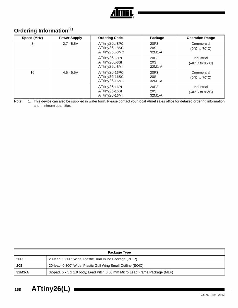
Note: 1. This device can also be supplied in wafer form. Please contact your local Atmel sales office for detailed ordering informationand minimum quantities.
Ordering Information(1)
Speed (MHz) Power Supply Ordering Code Package Operation Range
8 2.7 - 5.5V ATtiny26L-8PCATtiny26L-8SCATtiny26L-8MC
20P320S32M1-A
Commercial
(0°C to 70°C)
ATtiny26L-8PIATtiny26L-8SIATtiny26L-8MI
20P320S32M1-A
Industrial
(-40°C to 85°C)
16 4.5 - 5.5V ATtiny26-16PCATtiny26-16SCATtiny26-16MC
20P320S32M1-A
Commercial
(0°C to 70°C)
ATtiny26-16PIATtiny26-16SIATtiny26-16MI
20P320S32M1-A
Industrial
(-40°C to 85°C)
Package Type
20P3 20-lead, 0.300" Wide, Plastic Dual Inline Package (PDIP)
20S 20-lead, 0.300" Wide, Plastic Gull Wing Small Outline (SOIC)
32M1-A 32-pad, 5 x 5 x 1.0 body, Lead Pitch 0.50 mm Micro Lead Frame Package (MLF)
168 ATtiny26(L) 1477D–AVR–06/03

ATtiny26(L)
Packaging Information
20P3
2325 Orchard Parkway San Jose, CA 95131
TITLE DRAWING NO.
R
REV. 20P3, 20-lead (0.300"/7.62 mm Wide) Plastic Dual Inline Package (PDIP) B20P3
09/28/01
PIN1
E1
A1
B
E
B1
C
L
SEATING PLANE
A
D
e
eBeC
COMMON DIMENSIONS(Unit of Measure = mm)
SYMBOL MIN NOM MAX NOTE
A – – 5.334
A1 0.381 – –
D 25.984 – 25.493 Note 2
E 7.620 – 8.255
E1 6.096 – 7.112 Note 2
B 0.356 – 0.559
B1 1.270 – 1.551
L 2.921 – 3.810
C 0.203 – 0.356
eB – – 10.922
eC 0.000 – 1.524
e 2.540 TYP
Notes: 1. This package conforms to JEDEC reference MS-001, Variation AD. 2. Dimensions D and E1 do not include mold Flash or Protrusion.
Mold Flash or Protrusion shall not exceed 0.25 mm (0.010").
1691477D–AVR–06/03

20S
2325 Orchard ParkwaySan Jose, CA 95131
TITLE DRAWING NO.
R
REV. 20S2, 20-lead, 0.300" Wide Body, Plastic GullWing Small Outline Package (SOIC)
1/9/02
20S2 A
L
A1
End View
Side View
Top View
HE
b
N
1
e
A
D
C
COMMON DIMENSIONS(Unit of Measure = inches)
SYMBOL MIN NOM MAX NOTE
Notes: 1. This drawing is for general information only; refer to JEDEC Drawing MS-013, Variation AC for additional information.2. Dimension "D" does not include mold Flash, protrusions or gate burrs. Mold Flash, protrusions and gate burrs shall not exceed
0.15 mm (0.006") per side.3. Dimension "E" does not include inter-lead Flash or protrusion. Inter-lead Flash and protrusions shall not exceed 0.25 mm
(0.010") per side.4. "L" is the length of the terminal for soldering to a substrate.5. The lead width "b", as measured 0.36 mm (0.014") or greater above the seating plane, shall not exceed a maximum value of 0.61 mm
(0.024") per side.
A 0.0926 0.1043
A1 0.0040 0.0118
b 0.0130 0.0200 4
C 0.0091 0.0125
D 0.4961 0.5118 1
E 0.2914 0.2992 2
H 0.3940 0.4190
L 0.0160 0.050 3
e 0.050 BSC
170 ATtiny26(L) 1477D–AVR–06/03

ATtiny26(L)
32M1-A
2325 Orchard Parkway San Jose, CA 95131
TITLE DRAWING NO.
R
REV. 32M1-A, 32-pad, 5 x 5 x 1.0 mm Body, Lead Pitch 0.50 mm Micro Lead Frame Package (MLF) C32M1-A
01/15/03
COMMON DIMENSIONS(Unit of Measure = mm)
SYMBOL MIN NOM MAX NOTEPin 1 ID
D1
D
E1 E
eb
A3A2
A1 A
D2
E2
0.08 C
L
1
2
3
P
P
01
2
3
A 0.80 0.90 1.00
A1 – 0.02 0.05
A2 – 0.65 1.00
A3 0.20 REF
b 0.18 0.23 0.30
D 5.00 BSC
D1 4.75 BSC
D2 2.95 3.10 3.25
E 5.00 BSC
E1 4.75BSC
E2 2.95 3.10 3.25
e 0.50 BSC
L 0.30 0.40 0.50
P – – 0.60
– – 12oNote: JEDEC Standard MO-220, Fig. 2 (Anvil Singulation), VHHD-2.
TOP VIEW
SIDE VIEW
BOTTOM VIEW
0
Pin 1 ID
1711477D–AVR–06/03
Data Sheet Change Log for ATtiny26
Please note that the referring page numbers in this section are referred to this docu-ment. The referring revision in this section are referring to the document revision.
Changes from Rev. 1477A-03/02 to Rev. 1477B-04/02
1. Removed all references to Power Save sleep mode in the section “SystemClock and Clock Options” on page 25.
2. Updated the section “Analog to Digital Converter” on page 77 with moredetails on how to read the conversion result for both differential and single-ended conversion.
3. Updated “Ordering Information(1)” on page 168 and added MLF packageinformation.
Changes from Rev. 1477B-04/02 to Rev. 1477C-09/02
1. Changed the Endurance on the Flash to 10,000 Write/Erase Cycles.
Changes from Rev. 1477C-09/02 to Rev. 1477D-05/03
1. Updated “Packaging Information” on page 169.
2. Removed ADHSM from “ADC Characteristics – Preliminary Data” on page128.
3. Added section “EEPROM Write During Power-down Sleep Mode” on page 62.
4. Added section “Default Clock Source” on page 28.
5. Corrected PLL Lock value in the “Bit 0 – PLOCK: PLL Lock Detector” on page54.
6. Added information about conversion time when selecting differential chan-nels on page 80.
7. Corrected DDxn, PORTxn value on page 92.
8. Added section “Unconnected Pins” on page 95.
9. Added note for RSTDISBL Fuse in Table 49 on page 107.
10. Corrected DATA value in Figure 61 on page 115.
11. Added WD_FUSE period in Table 59 on page 122.
12. Updated “ADC Characteristics – Preliminary Data” on page 128 and addedTable 64, “ADC Characteristics, Differential Channels,” on page 129.
13. Updated “ATtiny26 Typical Characteristics – Preliminary Data” on page 130.
14. Added LPM Rd, Z and LPM Rd, Z+ in “Instruction Set Summary” on page 166.
172 ATtiny26(L) 1477D–AVR–06/03

ATtiny26(L)
Table of Contents Features................................................................................................. 1
Pin Configuration.................................................................................. 2Disclaimer ............................................................................................................. 2
Description ............................................................................................ 3Block Diagram ...................................................................................................... 4Pin Descriptions.................................................................................................... 5
Architectural Overview......................................................................... 6General Purpose Regist06/03er File .................................................................... 7ALU – Arithmetic Logic Unit.................................................................................. 8In-System Programmable Flash Program Memory .............................................. 9SRAM Data Memory............................................................................................. 9Program and Data Addressing Modes................................................................ 10EEPROM Data Memory...................................................................................... 14
Memory Access Times and Instruction Execution Timing ............. 15
I/O Memory .......................................................................................... 17Stack Pointer – SP.............................................................................................. 19Reset and Interrupt Handling.............................................................................. 20
System Clock and Clock Options ..................................................... 25Clock Systems and their Distribution .................................................................. 25Clock Sources..................................................................................................... 27Default Clock Source .......................................................................................... 28Crystal Oscillator................................................................................................. 28Low-frequency Crystal Oscillator ........................................................................ 29External RC Oscillator ........................................................................................ 30Calibrated Internal RC Oscillator ........................................................................ 31External Clock..................................................................................................... 32
Power Management and Sleep Modes.............................................. 41Minimizing Power Consumption ......................................................................... 43
Timer/Counters ................................................................................... 44Timer/Counter0 Prescaler................................................................................... 44Timer/Counter1 Prescaler................................................................................... 458-bit Timer/Counter0........................................................................................... 458-bit Timer/Counter1........................................................................................... 47
Watchdog Timer.................................................................................. 58
EEPROM Read/Write Access............................................................. 60Preventing EEPROM Corruption ........................................................................ 62
i1477D–AVR–06/03

Universal Serial Interface – USI......................................................... 63Overview............................................................................................................. 63Register Descriptions.......................................................................................... 64Functional Descriptions ...................................................................................... 68Alternative USI Usage ........................................................................................ 73
Analog Comparator ............................................................................ 74
Analog to Digital Converter ............................................................... 77Features.............................................................................................................. 77Operation ............................................................................................................ 78Prescaling and Conversion Timing ..................................................................... 79ADC Noise Canceler Function............................................................................ 82ADC Conversion Result...................................................................................... 82Scanning Multiple Channels ............................................................................... 88ADC Noise Canceling Techniques ..................................................................... 88Offset Compensation Schemes .......................................................................... 88
I/O Ports............................................................................................... 90Introduction ......................................................................................................... 90Ports as General Digital I/O ................................................................................ 91Alternate Port Functions ..................................................................................... 95Register Description for I/O Ports ..................................................................... 105
Memory Programming...................................................................... 106Program and Data Memory Lock Bits............................................................... 106Fuse Bits........................................................................................................... 107Signature Bytes ................................................................................................ 108Calibration Byte ................................................................................................ 108Parallel Programming Parameters, Pin Mapping, and Commands .................. 108Parallel Programming ....................................................................................... 111Serial Downloading........................................................................................... 120Serial Programming Pin Mapping ..................................................................... 120
Electrical Characteristics................................................................. 125Absolute Maximum Ratings*............................................................................. 125External Clock Drive Waveforms ...................................................................... 127External Clock Drive ......................................................................................... 127ADC Characteristics – Preliminary Data........................................................... 128
ATtiny26 Typical Characteristics – Preliminary Data.................... 130
ATtiny26(L) Register Summary ....................................................... 165
Instruction Set Summary ................................................................. 166
ii ATtiny26(L) 1477D–AVR–06/03
ATtiny26(L)
Ordering Information(1)..................................................................... 168
Packaging Information ..................................................................... 16920P3 ................................................................................................................. 16920S ................................................................................................................... 17032M1-A ............................................................................................................. 171
Data Sheet Change Log for ATtiny26 ............................................. 172Changes from Rev. 1477A-03/02 to Rev. 1477B-04/02 ................................... 172Changes from Rev. 1477B-04/02 to Rev. 1477C-09/02 ................................... 172Changes from Rev. 1477C-09/02 to Rev. 1477D-05/03................................... 172
Table of Contents .................................................................................. i
iii1477D–AVR–06/03

Printed on recycled paper.
Disclaimer: Atmel Corporation makes no warranty for the use of its products, other than those expressly contained in the Company’s standardwarranty which is detailed in Atmel’s Terms and Conditions located on the Company’s web site. The Company assumes no responsibility for anyerrors which may appear in this document, reserves the right to change devices or specifications detailed herein at any time without notice, anddoes not make any commitment to update the information contained herein. No licenses to patents or other intellectual property of Atmel aregranted by the Company in connection with the sale of Atmel products, expressly or by implication. Atmel’s products are not authorized for useas critical components in life support devices or systems.
Atmel Corporation Atmel Operations
2325 Orchard ParkwaySan Jose, CA 95131Tel: 1(408) 441-0311Fax: 1(408) 487-2600
Regional Headquarters
EuropeAtmel SarlRoute des Arsenaux 41Case Postale 80CH-1705 FribourgSwitzerlandTel: (41) 26-426-5555Fax: (41) 26-426-5500
AsiaRoom 1219Chinachem Golden Plaza77 Mody Road TsimshatsuiEast KowloonHong KongTel: (852) 2721-9778Fax: (852) 2722-1369
Japan9F, Tonetsu Shinkawa Bldg.1-24-8 ShinkawaChuo-ku, Tokyo 104-0033JapanTel: (81) 3-3523-3551Fax: (81) 3-3523-7581
Memory2325 Orchard ParkwaySan Jose, CA 95131Tel: 1(408) 441-0311Fax: 1(408) 436-4314
Microcontrollers2325 Orchard ParkwaySan Jose, CA 95131Tel: 1(408) 441-0311Fax: 1(408) 436-4314
La ChantrerieBP 7060244306 Nantes Cedex 3, FranceTel: (33) 2-40-18-18-18Fax: (33) 2-40-18-19-60
ASIC/ASSP/Smart CardsZone Industrielle13106 Rousset Cedex, FranceTel: (33) 4-42-53-60-00Fax: (33) 4-42-53-60-01
1150 East Cheyenne Mtn. Blvd.Colorado Springs, CO 80906Tel: 1(719) 576-3300Fax: 1(719) 540-1759
Scottish Enterprise Technology ParkMaxwell BuildingEast Kilbride G75 0QR, Scotland Tel: (44) 1355-803-000Fax: (44) 1355-242-743
RF/AutomotiveTheresienstrasse 2Postfach 353574025 Heilbronn, GermanyTel: (49) 71-31-67-0Fax: (49) 71-31-67-2340
1150 East Cheyenne Mtn. Blvd.Colorado Springs, CO 80906Tel: 1(719) 576-3300Fax: 1(719) 540-1759
Biometrics/Imaging/Hi-Rel MPU/High Speed Converters/RF Datacom
Avenue de RochepleineBP 12338521 Saint-Egreve Cedex, FranceTel: (33) 4-76-58-30-00Fax: (33) 4-76-58-34-80
Web Sitehttp://www.atmel.com
1477D–AVR–06/03 0M
© Atmel Corporation 2003. All rights reserved. Atmel® and combinations thereof, AVR® are the registeredtrademarks of Atmel Corporation or its subsidiaries. Other terms and product names may be the trademarks ofothers.