Dan Froelich Serial Enabling Workgroup Co-Chair onwards All Tx electrical ... – New template file...
52
Copyright © 2014, PCI-SIG, All Rights Reserved PCIe ® 3.0 Compliance Testing Dan Froelich Serial Enabling Workgroup Co-Chair 1
-
Upload
truongkhanh -
Category
Documents
-
view
222 -
download
5
Transcript of Dan Froelich Serial Enabling Workgroup Co-Chair onwards All Tx electrical ... – New template file...

Copyright © 2014, PCI-SIG, All Rights Reserved
PCIe® 3.0 Compliance Testing
Dan FroelichSerial Enabling Workgroup Co-Chair
1

PCIe Technology Seminar 2
PCIe® Compliance Program Status
PCIe Compliance Process
Compliance Test Overview
PCIe Electrical Tests and Tools
PCIe Protocol Testing
Platform BIOS Testing
PCIe Configuration Tests
Test Specification ECNs
Agenda
Copyright © 2014, PCI-SIG, All Rights Reserved

PCIe Technology Seminar
Compliance Program Overview
PCI™, PCI-X™, PCIe 1.x compliance testing no longer offered as of Jan 1, 2013
PCIe 2.0 compliance testing continues to be offered
Changes implemented starting with the April 2013 workshop
No changes to test cases or pass/fail criteria
All PCIECV testing to be done with 3.0 system and PCIECV 1.5.1.9 running on Windows 7
All BIOS testing to be run with 3.0 PTC card from April 2013 workshop onwards
All Tx electrical testing to be done using Sigtest 3.2
PCIe 3.0 official integrator’s list testing started in April 2013
Copyright © 2014, PCI-SIG, All Rights Reserved 3

PCIe Technology Seminar 4
Clear Test Output
Maps
Directly to Test
Spec
PCI-SIG® Specs
DescribesDevice Requirements
• 3.0 Base and CEM
specs
C&I Test Specs
DefineTest Criteria based on
spec requirements
•Test Definitions
• Pass/Fail Criteria
Test H/W & S/W
ValidatesTest Criteria
•Compliance
•Interoperability
PASS
FAILTest Tools
And Procedures
PCI-SIG
Specs
C&I
Test
Spec
Workshops
PCIe 3.0 Compliance Process
Predictable path to design compliance
Same process as 1.x, 2.xCopyright © 2014, PCI-SIG, All Rights Reserved
PCIe Technology Seminar 5
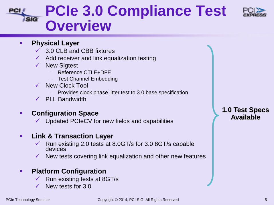
PCIe 3.0 Compliance Test Overview
Physical Layer 3.0 CLB and CBB fixtures
Add receiver and link equalization testing
New Sigtest– Reference CTLE+DFE
– Test Channel Embedding
New Clock Tool– Provides clock phase jitter test to 3.0 base specification
PLL Bandwidth
Configuration Space Updated PCIeCV for new fields and capabilities
Link & Transaction Layer Run existing 2.0 tests at 8.0GT/s for 3.0 8GT/s capable
devices
New tests covering link equalization and other new features
Platform Configuration Run existing tests at 8GT/s
New tests for 3.0
1.0 Test Specs Available
Copyright © 2014, PCI-SIG, All Rights Reserved

PCIe Technology Seminar 6
Compliance Workshop Overview
Workshops are usually announced 2 months in advance
Workshop registration closes 3 weeks prior for domestic, and 4 weeks prior for international
No on-site registration
Testing is done on devices using the standard CEM form factor
Device must past pass testing at a workshop in order to be listed on the PCI-SIG Integrators List
All required gold suite tests must pass
Interoperability testing
Interoperability testing
Opportunity for vendors at compliance workshop to test with each other
Goal is to demonstrate interoperability between products
80% passing rate required for eligibility for PCI-SIG Integrators List
Demonstrate that the link can train and operate at the highest common link speed supported
– For 2.0 devices, at 5GT/s if both devices support 5GT/s
– For 3.0 devices, at 8GT/s if both devices support 8GT/s
Copyright © 2014, PCI-SIG, All Rights Reserved

PCIe Technology Seminar
Electrical Tests
7Copyright © 2014, PCI-SIG, All Rights Reserved

PCIe Technology Seminar 8
Motherboard Test Procedure
CLB 2.0 Standard Test Fixture connected to slot under test
Lane under test and clock connected through fixture to oscilloscope
Motherboard under test enters compliance mode
– Fixture provides features to select different compliance speeds and de-emphasis levels
Data lane and reference clock sampled simultaneously
– 25 ps or smaller sample interval. At least 1 million UI.
Standard Post Processing Analysis Software (Sigtest 3.2)
– Supports All Common RT Scope Data Formats
– New template file DUAL_PORT_SYS_CON_250.dat posted for System Height ECN
Standard Test Procedures For Specific Test Equipment
OscilloscopeCLB 2.0 Motherboard − Capture waveform on oscilloscope
− Run signal analysis software
PCIe 2.0 Motherboard Electrical Tools
Same Basic Motherboard TX Test Setup/Process Used For 1.1 Program
Real-Time Scope, Post Processing Software, Compliance Mode, etc.
New 2.0 CEM Dual Port Method Test Clock and Data Simultaneously
Clock
Data
Copyright © 2014, PCI-SIG, All Rights Reserved

PCIe Technology Seminar 9
Oscilloscope
Add-in
Card CBB
− Capture waveform on oscilloscope
− Run signal analysis software
PCIe 2.0 Add-in CardElectrical Tools
Revised CBB for PCIe 1.1
Add-in Card Test Procedure
CBB 2.0 Standard Test Fixture with add-in card to test connected
Lane under test connected through fixture to oscilloscope
Add-in card under test enters compliance mode
– Fixture provides features to select different compliance speeds and de-emphasis levels
Data lane sampled
– 25 ps or smaller sample interval. At least 1 million UI
Standard Post Processing Analysis Software (Sigtest 3.2)
– Supports all common RT Scope data formats
Standard Test Procedures for specific test equipment
Same Basic AIC TX Test Setup/Process Used For 1.1 Testing
RT Scope, Post Processing Software, Compliance Mode, etc. Copyright © 2014, PCI-SIG, All Rights Reserved

PCIe Technology Seminar 10
PLL Bandwidth Testing
Required test for 2.0 Integrators List
Test outline
Sinusoidal phase jitter is added to reference clock from 0 to 25 Mhz in small frequency increments
– Reference clock jitter is calibrated to 43.6 ps under 2.0 spec filter
Transmitter jitter is measured at each point
3 dB point and peaking in transmitter response are determined from data
– 3 dB point must be between 8 and 16 Mhz with peaking < 3 dB peaking
– 3 dB point must be between 5 and 16 Mhz with peaking < 1 dB
Testing is repeated with reference clock jitter calibrated to 43.6/2 ps
Clock recovery method used at the compliance workshop
Spectrum analyzer method available as back-up upon request
Detailed procedures are available on website
8GT/s requirement– 3 dB point must be between 2 and 4 Mhz with peaking < 2 dB peaking
– 3 dB point must be between 2 and 5 Mhz with peaking < 1 dB
Copyright © 2014, PCI-SIG, All Rights Reserved

PCIe Technology Seminar 11
Endpoint 5GT/s Selectable De-emphasis Test
Endpoint must support 2 levels of de-emphasis at 5GT/s -3.5dB
-6dB
De-emphasis level selected by root port During link training to 5GT/s
Potential interoperability issue if endpoint does not respond to request
FYI for 2.0 IL. Required for 3.0 IL.
Two setups1. Setup similar to receiver testing using LeCroy PERT
2. PTC card + scope
RT scope captures waveform at L0 with each de-emphasis setting
Difference in average non-transition/transition voltage at eye center must be greater than 0.5 dB
Copyright © 2014, PCI-SIG, All Rights Reserved

PCIe Technology Seminar 12
PCIe 3.0 Required Electrical Tests
TX signal quality test at all supported link speeds (similar to 2.0 procedure)
PLL bandwidth
5.0GT/s selectable de-emphasis test
TX preset equalization test
8.0GT/s receiver test
Link equalization handshaking
Required TX adjustments
Requesting link partner to adjust if needed
Copyright © 2014, PCI-SIG, All Rights Reserved
Detailed test equipment specific test procedures for Tx and Rx testing available at PCI-SIG website

PCIe Technology Seminar
3.0 Receiver Tests
Rx Jitter Tolerance
Rotating between Agilent, LeCroy, and Tektronix test equipment
Run at 8GT/s
DUT is placed into loopback
DUT selects TX EQ for test equipment
Monitor bit stream for errors
Test at E-4 with allowed MB presets (Add-in Cards)
– Presets P7 and P8 with 16” – two connector test channel
Rx link equalization tests
Details in a later slide
13Copyright © 2014, PCI-SIG, All Rights Reserved
PCIe Technology Seminar 14
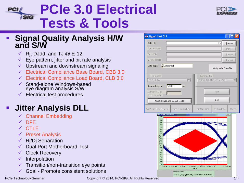
Signal Quality Analysis H/W and S/W Rj, DJdd, and TJ @ E-12
Eye pattern, jitter and bit rate analysis
Upstream and downstream signaling
Electrical Compliance Base Board, CBB 3.0
Electrical Compliance Load Board, CLB 3.0
Stand-alone Windows-basedeye diagram analysis S/W
Electrical test procedures
Jitter Analysis DLL Channel Embedding
DFE
CTLE
Preset Analysis
Rj/Dj Separation
Dual Port Motherboard Test
Clock Recovery
Interpolation
Transition/non-transition eye points
Goal - Promote consistent solutions
PCIe 3.0 Electrical Tests & Tools
Copyright © 2014, PCI-SIG, All Rights Reserved

PCIe Technology Seminar
3.0 Add-in Card
Test Fixture
Name Description Name Description
cbb_conn1 Connector cbb_via Via
cbb_rt5 4.0” Riser cbb_rt7 10.0”, Main routing
cbb_conn2 Connector cbb_rt8 0.8”, Package Breakout
cbb_rt60.2”, Connector Breakout
tx_spkg Package, 1.3”
cbb_via
cbb_rt6
cbb_rt7
tx_spkg
cbb_conn2
cbb_rt8
RX SMP
cbb_rt
5cbb_rt
5
cbb_conn1TX SMP
Main Board
Riser Board
Long Fixture Channel Approximates Worst Case Real Channel Improving
Correlation
15Copyright © 2014, PCI-SIG, All Rights Reserved

PCIe Technology Seminar
3.0 Add-in Card Rx Test Calibration
rx_spkg
cbb_conn2
RX SMP
cbb_conn1TX SMP
Test
Equipment
CLB 3.0
Post Processing S/W
(Embed RX pkg + use
behavioral EQ)
Signal
Generator
Sj + Rj +
Diff Noise
TXRX
16Copyright © 2014, PCI-SIG, All Rights Reserved

PCIe Technology Seminar
3.0 Add-in Card Rx Test Setup
rx_spkg
cbb_conn2
RX SMP
cbb_conn1TX SMP
Error
Detector
AIC Under Test
Signal
Generator
Sj + Rj +
Diff Noise
17Copyright © 2014, PCI-SIG, All Rights Reserved

PCIe Technology Seminar
Link Equalization Tests
Requires protocol-aware test equipment
LeCroy PERT used
TX link equalization response test
Use protocol-aware test equipment to request a Tx equalization change
Check that the DUT responds and sets its Tx to the correct preset within required time period
Measurement of DUT Tx done by going to loopback and sending compliance pattern
Do this check for all presets
Rx link equalization
Calibration the same as standard RX test
Start with a non-optimal Tx equalization setting (P7 or P8)
Allow DUT to request for equalization adjustments
Place DUT into loopback
Monitor bit stream for errors
18Copyright © 2014, PCI-SIG, All Rights Reserved

PCIe Technology Seminar
CBB 3.0
19
Add-in card
TX lanes
Power ResetCompliance
Mode Selection
Connect to
CBB Riser
Clock
Injection
Copyright © 2014, PCI-SIG, All Rights Reserved

PCIe Technology Seminar
CBB 3.0 Riser
20
Add-in card
RX lanes
Connect to
CBB main
board
Copyright © 2014, PCI-SIG, All Rights Reserved

PCIe Technology Seminar
CLB 3.0
Copyright © 2014, PCI-SIG, All Rights Reserved 21
X4/x8 CLB
X1/x16 CLB

PCIe Technology Seminar
Protocol Testing
22Copyright © 2014, PCI-SIG, All Rights Reserved

PCIe Technology Seminar 23
FPGA RA
MPGM
USB
PCI Express®
Transaction
Layer
Link
Layer
Physical
Layer
DUT
Protocol
Test
Card
Test Control software running on platform or Device Under Test (DUT) initiates test traffic
PTC monitors and acts on that traffic
Checking protocol
Injecting errors
PCIe Protocol Testing
Copyright © 2014, PCI-SIG, All Rights Reserved
PCIe Technology Seminar 24
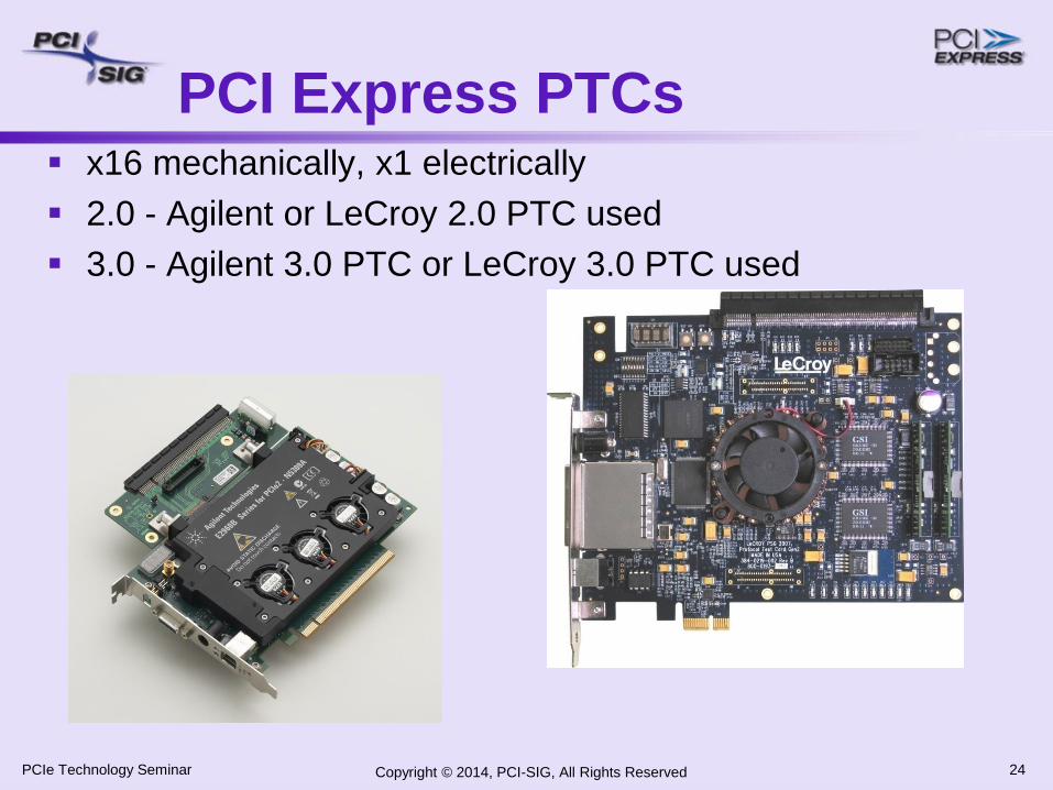
PCI Express PTCs x16 mechanically, x1 electrically
2.0 - Agilent or LeCroy 2.0 PTC used
3.0 - Agilent 3.0 PTC or LeCroy 3.0 PTC used
Copyright © 2014, PCI-SIG, All Rights Reserved

PCIe Technology Seminar 25
PCIe Link / Transaction Compliance Tests
Described in Link Layer Test Spec and Transaction Layer Test Spec
Merged test spec for 3.0
Speed requirement
Must be run at highest supported link speed
Tests (from 1.x) Reserved fields – Device ignores them
NAK response – Device will resend after receiving NAK
Replay Timers – Device will resend packet if no response
Replay Count – Device will resend multiple times when no response
Link Retrain – Device will retrain if continued no response
Replay TLP order – Device replays TLPs in proper order
Bad CRC – Device detects, drops, and logs (DLLPs & TLPs)
Undefined packet – Device ignores
Bad Sequence Number – Device detects, drops, and logs
Duplicate TLP – Device returns data once
Request Completion – Issue UR for config requests not supported
Copyright © 2014, PCI-SIG, All Rights Reserved
PCIe Technology Seminar
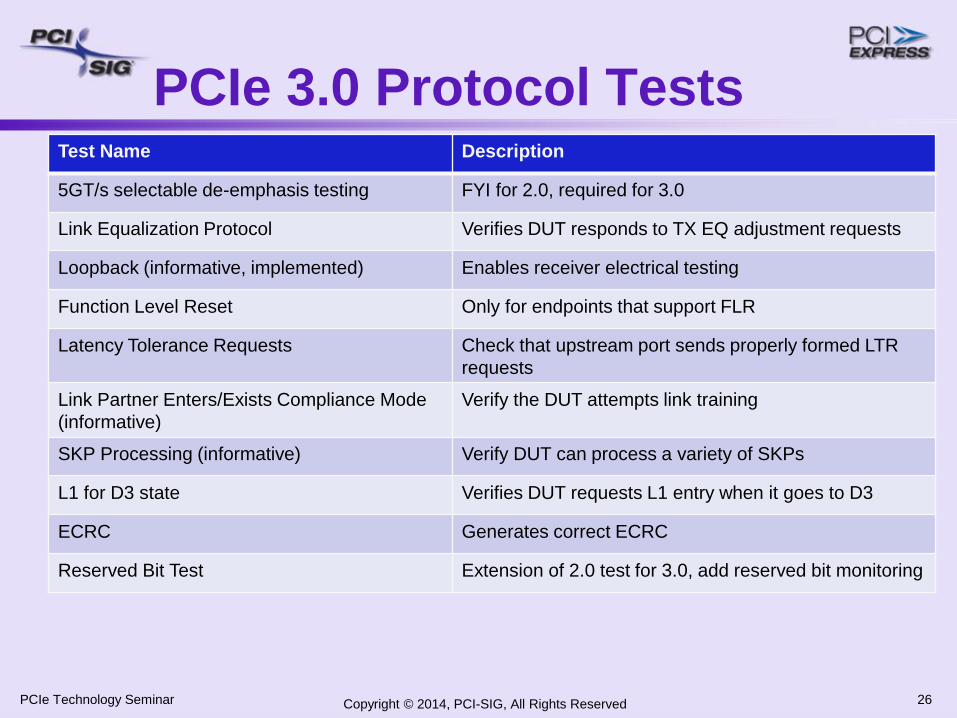
Test Name Description
5GT/s selectable de-emphasis testing FYI for 2.0, required for 3.0
Link Equalization Protocol Verifies DUT responds to TX EQ adjustment requests
Loopback (informative, implemented) Enables receiver electrical testing
Function Level Reset Only for endpoints that support FLR
Latency Tolerance Requests Check that upstream port sends properly formed LTR
requests
Link Partner Enters/Exists Compliance Mode
(informative)
Verify the DUT attempts link training
SKP Processing (informative) Verify DUT can process a variety of SKPs
L1 for D3 state Verifies DUT requests L1 entry when it goes to D3
ECRC Generates correct ECRC
Reserved Bit Test Extension of 2.0 test for 3.0, add reserved bit monitoring
26
PCIe 3.0 Protocol Tests
Copyright © 2014, PCI-SIG, All Rights Reserved

PCIe Technology Seminar
Platform BIOS Testing
Copyright © 2014, PCI-SIG, All Rights Reserved 27

PCIe Technology Seminar
Platform BIOS Testing
Protocol Test Card Can Represent Any
Hierarchical Multi- Device/Bridge Topology
Device Decodes All Type 0 and Type 1
Configuration Cycles
Copyright © 2014, PCI-SIG, All Rights Reserved 28
UsbProtocol
Test CardSystem Under
Test
Control
System
All BIOS testing run using 3.0 PTC at workshops
Host
Protocol Test Card
(Acts like a Switch)
Emulated
Devices

PCIe Technology Seminar
PCIe BIOS Test
Copyright © 2014, PCI-SIG, All Rights Reserved 29
Multiple Functions per device
Different BAR combinations I/O, Mem, 64bit
Various size requests
Prefetchable, non-prefetchable
Bridges With Resource Requests
ASPM Configurations
Option ROMs Varying sizes
Different for each device function
Shrinkable, removable
Complex Multiple Switch and Bridge Topologies
2.0 updates: Use 3.0 PTC
No functional changes since 1.1
Run at 5.0GT/s as FYI

PCIe Technology Seminar
3.0 BIOS Tests
Copyright © 2014, PCI-SIG, All Rights Reserved 30
New capabilities present in devices (ACS, IOV, etc…)
Max payload size
All functions of a multi-function device are set to the same max payload size
Common clock test
Common clock config bit should be set to the same on both sides of the link
Slot Power Test
Configure x16 slots with >25W
ASPM optionality (new for 3.0)
Only enable ASPM (L0s or L1) if both sides support it
VC mapping
TC mapped to only one VC
Clock power management
Should not be enabled on CEM form factor
Review the test spec for details!
Full PCIe 3.0 Bios Tests Available at Workshops

PCIe Technology Seminar
Configuration Tests
31Copyright © 2014, PCI-SIG, All Rights Reserved
PCIe Technology Seminar
Copyright © 2014, PCI-SIG, All Rights Reserved 32
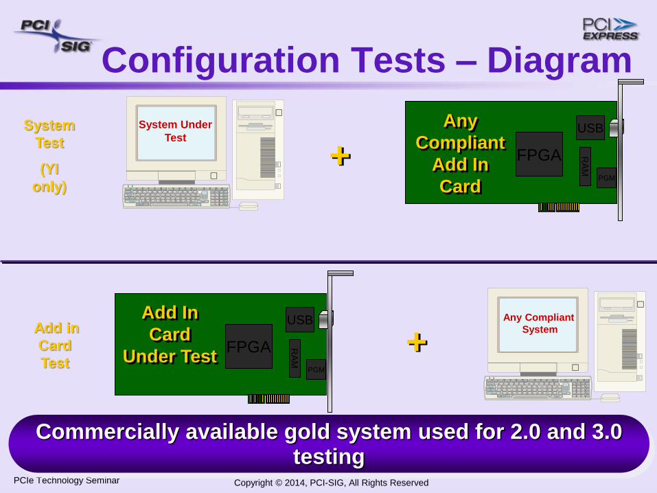
Configuration Tests – Diagram
System Under
Test
Any
Compliant
Add In
Card
FPGA RA
M
PGM
USB
+
Any Compliant
System
+Add In
Card
Under TestFPGA R
AM
PGM
USB
System
Test
(YI
only)
Add in
Card
Test
Commercially available gold system used for 2.0 and 3.0 testing
Copyright © 2014, PCI-SIG, All Rights Reserved

PCIe Technology Seminar 33
PCIECV – 2.0 Link Speed Test
Gold System 5GT/s capable, 2.0 spec compliant system used for testing add-in
cards
Set target link speed to limit maximum link speed and then write retrain link bit. Disable autonomous width or bandwidth changes on both components Upstream 2.5 Downstream 5.0 Result 2.5
Upstream 5.0 Downstream 5.0 Result 5.0
Test criteria Autonomous Bandwidth Status must never be set
Config registers must never be reset
Actual link speed matches expected link speed
Copyright © 2014, PCI-SIG, All Rights Reserved

PCIe Technology Seminar 34
CEM 2.0 spec requires x4 and x8 to be supported as intermediate widths
Specified in 2.0 Config test spec
Testing only static link width support
Use low cost mechanical adaptors to do all testing with standard x16 slot
Insert in riser card, and check that the
link comes up in the correct link width
PCIECV – 2.0 Link Width Test
Copyright © 2014, PCI-SIG, All Rights Reserved

PCIe Technology Seminar 35
PCI Express 3.0 Config Tests
PCIECV 3.0 update released
2.1 spec updates
– E.g. ARI, DPA, Resizable BAR, Multi-cast, LTR, TPH extended capabilities
Run tests at 8GT/s
3.0 config space updates
– Secondary PCI Express extended capability
IOV Capabilities
– E.g. ATS Extended Cap, SR-IOV extended cap
PCIECV 1.5.2.4 update released
Review the test spec for details!
Full PCIECV 3.0 version available at workshopsCopyright © 2014, PCI-SIG, All Rights Reserved

PCIe Technology Seminar
Test Spec ECNs
PLL Bandwidth Test Limits ECN
Relax PLL test limits to +/-0.5MHz and +0.25dB
Implemented at workshops starting in 2014
Extended TPH enable bit can be hardwired to 0 if extended TPH is not supported
ECN to base spec approved by the PWG
Config test spec ECN in progress
Currently treated as an exception
To be fixed in next release of PCIECV
BadECRC PTC test
ECN to base spec approved by PWG that flow control credits be updated when TLP with bad ECRC is received is recommended but not required
Test spec ECN in progress
Preliminary updated PTC test available
Copyright © 2014, PCI-SIG, All Rights Reserved 36

PCIe Technology Seminar 37
PCI Express 2.0 Compliance
PCI Express 1.1 Compliance
PCIe Compliance Summary
PCI Express 3.0 base specification available now Your compatible architecture for new designs!
PCI Express 2.0 Integrators List testing started in September 2008
PCI Express 3.0 Integrators List testing started April 2013
PCI Express 2.0 and 3.0 testing collateral available on PCI-SIG website
For all PCI Express material, visit www.pcisig.com
PCI Express 1.0a Compliance
2005-2006 2007-2008 2009-2010 2011-2012 2013-2014 2014-2015
Copyright © 2014, PCI-SIG, All Rights Reserved
PCI Express 3.0
Compliance

PCIe Technology Seminar 38
Thank you for attending the PCIe Technology Seminar.
For more information please go to www.pcisig.com
Copyright © 2014, PCI-SIG, All Rights Reserved

39
Backup

PCIe Technology Seminar 40
2.0 FYI Endpoint Receiver Sensitivity Test
Reduced motherboard voltage height requirement 2.0 CEM Spec ECN released
– From 300 mV to 250 mV
– Note – 3.0 CEM spec reduced to 225 mV
FYI Add-in Card Receiver Sensitivity Test Procedure Connect add-in card (DUT) to modified 2.0 CBB
– Modify RX lane zero on CBB to isolate toggle circuit
Connect test equipment output to DUT RX Lane zero
Connect DUT TX Lane zero to test equipment receiver
Test equipment sends training set sequence to send DUT to loopback state
Test equipment sends compliance pattern to DUT
Set test equipment outputs to maximum jitter allowed by CEM 2.0 spec
Test equipment monitors the compliance pattern from DUT Tx for errors
Sweep voltage margin and Sj jitter frequency to find failure margin for each Sj frequency– Measure eye opening at each failure point by removing DUT and adding CLB test
fixture and performing standard Motherboard eye test
Copyright © 2014, PCI-SIG, All Rights Reserved

PCIe Technology Seminar 41
PCIe 1.1 Compliance Test Areas
Physical layer
Examine electrical signaling
Configuration Space
Verify required fields and values
Link & Transaction layer
Exercise protocol boundary conditions
Inject errors and check error handling
Platform Configuration
Check BIOS handling of PCI Express devices
Available on PCI-SIG
website
Copyright © 2014, PCI-SIG, All Rights Reserved

PCIe Technology Seminar 42
CLB 2.0 (Compliance) FeaturesX1 Ref Clk
Probing
Points
X16 Ref Clk
Probing Points
Compliance Mode(x16)
Toggle Switch
Compliance
Mode(x1) Toggle
Switch
x16 RefClk / Toggle-
Mode Selector
x1 RefClk / Toggle-Mode
Selector
X1/ X16 Selection
x1 TX SMPs
Copyright © 2014, PCI-SIG, All Rights Reserved

PCIe Technology Seminar 43
CBB 2.0 FeaturesCompliance Mode Selection
Power Reset
Add-in card
RX lanes
Add-in card
TX lanes
Resistor stuffing
Option
Clock Noise
Injection
External REFCLK
Injection
CBB and CLB
2.0 Versions
Can be Used
for 2.5GT/s
Testing
Copyright © 2014, PCI-SIG, All Rights Reserved

PCIe Technology Seminar 44
x8 Edge & Active
Probing
x16 Edge &
Active Probing
x1 Tx SMA
Probing
x16 Tx
SMA Probing
x4 Edge
x16 RefClk Probing
x4 RefClk
Probing
x4 Tx SMA
Probing
x1 Edge
x8 SMA
Probingx1 RefClk
Probing
CLB For PCI Express 1.x(Used for 1.1 Integrators List Testing)
Copyright © 2014, PCI-SIG, All Rights Reserved

PCIe Technology Seminar 45
x16 Test Slot
100Mhz Clk
(CK410)
Clk Buffer
(DB800) External Clock
Input
x16 Rx
Inputs
x16 Tx
Active
Probing
x16 Tx
SMA Probing
Current
Probing
ATX PS
Clock Noise
Injection
Low Jitter Clean
Clock
Power
Switch
CBB For PCI Express 1.1(Used for 1.1 Integrators List Testing)
Copyright © 2014, PCI-SIG, All Rights Reserved

PCIe Technology Seminar 46
Clean Clock 1.1 Add-in Card Testing
1.1 Compliance base board built to have a RefClk with very little jitter
Provides accurate picture of device-under-test jitter
2.0 CBB offers lower jitter clock and continues 1.1 clean clock add-in card test model
For test fixture availability, visit www.pcisig.com
Copyright © 2014, PCI-SIG, All Rights Reserved

PCIe Technology Seminar 47
CLB 2.0 Updates
SMP Connectors
Two Versions x1, x16
x4, x8
SMP Connectors and Probe Points For Ref Clock
Compliance Mode Toggle Mechanism 2.5GT/s
5.0GT/s at -3.5 dB and -6.0 dB
85 Ohm Traces
Copyright © 2014, PCI-SIG, All Rights Reserved

PCIe Technology Seminar 48
PCI Express x1 connector to fit
into host platform slots of any
lane widthx1 edge – Platform side
USB2.0
x16 with x1
Connection
Power from
System
PCIe 1.x Protocol Test Card (PTC)
Copyright © 2014, PCI-SIG, All Rights Reserved

PCIe Technology Seminar 49
Worst Case Topology
Copyright © 2014, PCI-SIG, All Rights Reserved

PCIe Technology Seminar 50
The following is available on www.pcisig.com:
Link/Transaction– Agilent and Lecroy 2.0 PTC ordering information
– Agilent and Lecroy test procedures
– Agilent and Lecroy test software
Electrical– CBB 2.0 / CLB 2.0 availability and ordering information
– Sigtest 3.1.9
– Procedures using RT Scope
– PLL bandwidth test procedures
Config– PCIeCV 1.4.6
– Test procedure
PCIe 2.0 Compliance Test Summary
Copyright © 2014, PCI-SIG, All Rights Reserved

PCIe Technology Seminar 51
PCIe 1.1 Compliance SummaryDevice Type
Test Endpoint Root Switch / Bridge
Physical Layer (Electrical)
- Sigtest 2.1
- CBB / CLB 1.1
- PCI Express Electrical Test Consideration (1.1)
- Test procedures for RT scopes Required Required Required
Configuration Space
- PCIECV 1.3
- PCI Express Configuration Test Consideration (1.1)
- PCI Express Configuration Test Procedure (1.1) Required Required
Link and Transaction Layer
- 1.1 PTC
- PTC test software 1.1.0.16
- PCI Express Test Considerations - Link Layer
- PCI Express Test Considerations - Transaction Layer
- PCI Express Link/Transaction Test Procedures Required Required
Clock Jitter
- ClockTool version 1.3 FYI only
Platform BIOS Test
- 1.1 PTC
- PCI Express Platform BIOS Test Software v0.90 Required
Interoperability Testing (80%) Required Required Required
Copyright © 2014, PCI-SIG, All Rights Reserved

PCIe Technology Seminar 52
PCIe 2.0 Compliance SummaryDevice Type
Test Endpoint Root Switch / Bridge
Physical Layer (Electrical)
- Sigtest 3.1.9
- CBB / CLB 2.0
- PCI Express PHY Test Spec 2.0
- Test procedures for RT scopes Required Required Required
PLL BW Testing Required Required
Configuration Space
- PCIECV 1.4.6
- PCI Express Configuration Test Spec 2.0
- PCI Express Configuration Test Procedure 2.0 Required Required
Link and Transaction Layer
- 2.0 PTC
- PTC test software
- PCI Express Link Layer Test Spec 2.0
- PCI Express Transaction Layer Test Spec 2.0
- PCI Express Link/Transaction Test Procedures 2.0 Required Required
Clock Jitter
- ClockTool version 1.3 FYI only
Platform BIOS Test
- 1.1 PTC
- PCI Express Platform BIOS Test Software v0.90 Required
Interoperability Testing (80%) Required Required Required
Copyright © 2014, PCI-SIG, All Rights Reserved