
DA14681 Low Power Bluetooth Smart 4.2 SoC …...An on-chip PLL enables on-the-fly tuning of the...
460
Datasheet Revision 2.1 15-July-2016 CFR0011-120-00-FM Rev 5 1 of 460 © 2016 Dialog Semiconductor DA14681 Low Power Bluetooth Smart 4.2 SoC PRELIMINARY General description The DA14681 is a flexible System-on-Chip combining an application processor, memories, cryptography engine, power management unit, digital and analog peripherals and a Bluetooth ® Smart MAC engine and radio transceiver. The DA14681 is based on an ARM ® Cortex ® -M0 CPU delivering up to 84 DMIPS and provides a flexible memory architecture, enabling code execution from embedded memory (RAM, ROM) or non-volatile mem- ory (OTP or external Quad-SPI FLASH). The advanced power management unit of the DA14681 enables it to run from primary and secondary batteries, as well as provide power to external devices. The on-chip charger and state-of-charge fuel gauge allow the DA14681 to natively charge rechargeable batteries over USB. An on-chip PLL enables on-the-fly tuning of the system clock between 32 kHz and 96 MHz to meet high pro- cessing requirements. Several optimised sleep modes are available to reduce power dissipation when there is no activity. Features Complies to Bluetooth v4.2, ETSI EN 300 328 and EN 300 440 Class 2 (Europe), FCC CFR47 Part 15 (US) and ARIB STD-T66 (Japan) Flexible processing power 0 Hz up to 96 MHz 32-bit ARM Cortex-M0 with 4-way associative cache Three optimised power modes (Extended sleep, Deep sleep and Hibernation) reducing current to 1.4 uA Memories 64 kB One-Time-Programmable (OTP) memory 128 kB Data SRAM with retention capabilities 16 kB Cache SRAM with retention capabilities 128 kB ROM (including boot ROM and BLE stack) Power management Integrated Buck DC-DC converter (1.7 V - 4.75 V) Three power supply pins for external devices Supports Li-Polymer, Li-Ion, coin, NiMH and alka- line batteries Charger (up to 5.0 V) with programmable curves High accuracy state-of-charge fuel gauge Programmable threshold for brownout detection Digitally controlled oscillators and PLL 16 MHz crystal oscillator 16 MHz RC oscillator 32 kHz crystal and RC oscillator 10.5 kHz RCX oscillator Low power PLL up to 96 MHz Three general purpose timer/counters with PWM One 16-bit up/down timer/counter with PWM available in extended/deep sleep mode Application cryptographic engine with ECC, AES- 256, SHA-1, SHA-256, SHA-512 and True Random Number Generator Digital interfaces 37 (AQFN) or 21 (WLCSP) general purpose I/Os with programmable voltage levels Quad-SPI FLASH interface Two UARTs, one with hardware flow control Two SPI+™ interfaces Two I2C bus interfaces at 100 kHz, 400 kHz Three-axes capable Quadrature Decoder PDM + HW decimator (2 mics or 2 speakers) I2S/PCM master/slave interface up to 8 channels Keyboard scanner with debouncing Infrared (IR) interface (PWM) USB 1.1 Full Speed (FS) device interface Analog interfaces 8-channel 10-bit ADC with averaging capability Three matched white LED drivers Temperature sensor Radio transceiver 2.4 GHz CMOS transceiver with integrated balun 50 matched single wire antenna interface 0 dBm transmit output power -94 dBm receiver sensitivity (BLE) Supply current at VBAT1 (3 V): TX: 3.4 mA RX: 3.1 mA (with ideal DC-DC converter) Packages: AQFN with 60 pins, 6 mm x 6 mm WLCSP with 53 balls, 3.406 mm x 3.010 mm ________________________________________________________________________________________________ System diagram
Transcript of DA14681 Low Power Bluetooth Smart 4.2 SoC …...An on-chip PLL enables on-the-fly tuning of the...

Datasheet Revision 2.1 15-July-2016
CFR0011-120-00-FM Rev 5 1 of 460 © 2016 Dialog Semiconductor
DA14681
Low Power Bluetooth Smart 4.2 SoC PRELIMINARY
General descriptionThe DA14681 is a flexible System-on-Chip combiningan application processor, memories, cryptographyengine, power management unit, digital and analogperipherals and a Bluetooth® Smart MAC engine andradio transceiver.
The DA14681 is based on an ARM® Cortex®-M0 CPUdelivering up to 84 DMIPS and provides a flexiblememory architecture, enabling code execution fromembedded memory (RAM, ROM) or non-volatile mem-ory (OTP or external Quad-SPI FLASH).
The advanced power management unit of theDA14681 enables it to run from primary and secondarybatteries, as well as provide power to external devices.The on-chip charger and state-of-charge fuel gaugeallow the DA14681 to natively charge rechargeablebatteries over USB.
An on-chip PLL enables on-the-fly tuning of the systemclock between 32 kHz and 96 MHz to meet high pro-cessing requirements. Several optimised sleep modesare available to reduce power dissipation when there isno activity.
Features Complies to Bluetooth v4.2, ETSI EN 300 328 and
EN 300 440 Class 2 (Europe), FCC CFR47 Part 15 (US) and ARIB STD-T66 (Japan)
Flexible processing power 0 Hz up to 96 MHz 32-bit ARM Cortex-M0 with
4-way associative cache Three optimised power modes (Extended sleep,
Deep sleep and Hibernation) reducing current to 1.4 uA
Memories 64 kB One-Time-Programmable (OTP) memory 128 kB Data SRAM with retention capabilities 16 kB Cache SRAM with retention capabilities 128 kB ROM (including boot ROM and BLE stack)
Power management Integrated Buck DC-DC converter (1.7 V - 4.75 V) Three power supply pins for external devices Supports Li-Polymer, Li-Ion, coin, NiMH and alka-
line batteries Charger (up to 5.0 V) with programmable curves High accuracy state-of-charge fuel gauge Programmable threshold for brownout detection
Digitally controlled oscillators and PLL 16 MHz crystal oscillator 16 MHz RC oscillator 32 kHz crystal and RC oscillator 10.5 kHz RCX oscillator Low power PLL up to 96 MHz
Three general purpose timer/counters with PWM One 16-bit up/down timer/counter with PWM
available in extended/deep sleep mode Application cryptographic engine with ECC, AES-
256, SHA-1, SHA-256, SHA-512 and True Random Number Generator
Digital interfaces 37 (AQFN) or 21 (WLCSP) general purpose I/Os
with programmable voltage levels Quad-SPI FLASH interface Two UARTs, one with hardware flow control Two SPI+™ interfaces Two I2C bus interfaces at 100 kHz, 400 kHz Three-axes capable Quadrature Decoder PDM + HW decimator (2 mics or 2 speakers) I2S/PCM master/slave interface up to 8 channels Keyboard scanner with debouncing Infrared (IR) interface (PWM) USB 1.1 Full Speed (FS) device interface
Analog interfaces 8-channel 10-bit ADC with averaging capability Three matched white LED drivers Temperature sensor
Radio transceiver 2.4 GHz CMOS transceiver with integrated balun 50 matched single wire antenna interface 0 dBm transmit output power -94 dBm receiver sensitivity (BLE) Supply current at VBAT1 (3 V):
TX: 3.4 mARX: 3.1 mA (with ideal DC-DC converter)
Packages: AQFN with 60 pins, 6 mm x 6 mm WLCSP with 53 balls, 3.406 mm x 3.010 mm
________________________________________________________________________________________________
System diagram

Datasheet Revision 2.1 15-July-2016
CFR0011-120-00-FM Rev 5 2 of 460 © 2016 Dialog Semiconductor
DA14681
Low Power Bluetooth Smart 4.2 SoC PRELIMINARY
1 Block diagram . . . . . . . . . . . . . . . . . . . . . . . . . . . . . . 6
2 Package and pinout . . . . . . . . . . . . . . . . . . . . . . . . . 7
3 System overview . . . . . . . . . . . . . . . . . . . . . . . . . . . 19
3.1 INTERNAL BLOCKS . . . . . . . . . . . . . . . . . . . . 19
3.2 FUNCTIONAL MODES . . . . . . . . . . . . . . . . . . 20
3.3 SYSTEM CONFIGURATION . . . . . . . . . . . . . 20
3.4 SYSTEM STARTUP PROCEDURE . . . . . . . . 23
3.4.1 Power/Wakeup FSM . . . . . . . . . . . . . . . 24
3.4.2 Goto Sleep FSM . . . . . . . . . . . . . . . . . . 24
3.4.3 BootROM sequence . . . . . . . . . . . . . . . 25
3.5 POWER CONTROL AND MODES . . . . . . . . . 27
3.5.1 System Power Control . . . . . . . . . . . . . . 27
3.5.2 Power domains . . . . . . . . . . . . . . . . . . . 28
3.5.3 Power modes. . . . . . . . . . . . . . . . . . . . . 29
4 Power management . . . . . . . . . . . . . . . . . . . . . . . . 31
4.1 ARCHITECTURE . . . . . . . . . . . . . . . . . . . . . . 31
4.1.1 SIMO DC-DC converter . . . . . . . . . . . . . 32
4.1.2 LDOs . . . . . . . . . . . . . . . . . . . . . . . . . . . 34
4.1.3 Switching from DC-DC to LDOs . . . . . . 36
4.1.4 PMU configurations in Sleep modes . . . 37
4.1.5 Wake/Power up - Sleep Timing . . . . . . . 37
4.1.6 Charger . . . . . . . . . . . . . . . . . . . . . . . . . 40
4.1.7 Fuel gauge. . . . . . . . . . . . . . . . . . . . . . . 42
4.1.8 USB charger detection. . . . . . . . . . . . . . 44
5 Reset. . . . . . . . . . . . . . . . . . . . . . . . . . . . . . . . . . . . . 47
5.1 POR, HW AND SW RESET . . . . . . . . . . . . . . 47
5.2 BROWN OUT DETECTION . . . . . . . . . . . . . . 48
6 Clock generation . . . . . . . . . . . . . . . . . . . . . . . . . . . 49
6.1 CLOCK TREE . . . . . . . . . . . . . . . . . . . . . . . . . 49
6.2 CRYSTAL OSCILLATORS . . . . . . . . . . . . . . . 50
6.2.1 Frequency control (16 MHz crystal) . . . . 50
6.2.2 Automated trimming and settling notification
50
6.3 RC OSCILLATORS . . . . . . . . . . . . . . . . . . . . . 51
6.3.1 Frequency calibration . . . . . . . . . . . . . . 52
6.4 PLL . . . . . . . . . . . . . . . . . . . . . . . . . . . . . . . . . 52
7 ARM Cortex M0 . . . . . . . . . . . . . . . . . . . . . . . . . . . . 53
7.1 SYSTEM TIMER (SYSTICK). . . . . . . . . . . . . . 54
7.2 WAKEUP INTERRUPT CONTROLLER . . . . . 54
7.3 REFERENCE . . . . . . . . . . . . . . . . . . . . . . . . . 54
7.4 INTERRUPTS . . . . . . . . . . . . . . . . . . . . . . . . . 55
8 Cache Controller . . . . . . . . . . . . . . . . . . . . . . . . . . . 57
8.1 CACHABLE RANGE . . . . . . . . . . . . . . . . . . . . 57
8.2 RUNTIME RECONFIGURATION . . . . . . . . . . 58
8.2.1 Cache Line reconfiguration . . . . . . . . . . 58
8.2.2 TAG memory word . . . . . . . . . . . . . . . . . 58
8.2.3 Associativity reconfiguration . . . . . . . . . 58
8.3 2 AND 4 WAY REPLACEMENT STRATEGY . 58
8.4 CACHE RESETS. . . . . . . . . . . . . . . . . . . . . . . 58
8.5 CACHE MISS RATE MONITOR . . . . . . . . . . . 59
8.6 CACHE MISS LATENCY AND POWER . . . . . 59
9 AMBA Bus . . . . . . . . . . . . . . . . . . . . . . . . . . . . . . . . 61
10 Memory Controller . . . . . . . . . . . . . . . . . . . . . . . . 63
11 OTP Controller. . . . . . . . . . . . . . . . . . . . . . . . . . . . 65
11.1 OPERATING MODES . . . . . . . . . . . . . . . . . . 65
11.2 AHB MASTER INTERFACE . . . . . . . . . . . . . 66
11.3 AHB SLAVE INTERFACES . . . . . . . . . . . . . . 66
11.4 ERROR CORRECTING CODE (ECC) . . . . . 66
11.5 BUILD-IN SELF REPAIR (BISR) . . . . . . . . . . 66
12 Quad SPI Controller . . . . . . . . . . . . . . . . . . . . . . . 67
12.1 ARCHITECTURE . . . . . . . . . . . . . . . . . . . . . 67
12.1.1 Interface. . . . . . . . . . . . . . . . . . . . . . . . 67
12.1.2 Initialization FSM . . . . . . . . . . . . . . . . . 68
12.1.3 SPI modes . . . . . . . . . . . . . . . . . . . . . . 69
12.1.4 Access modes . . . . . . . . . . . . . . . . . . . 69
12.1.5 Endianess . . . . . . . . . . . . . . . . . . . . . . 69
12.1.6 Erase Suspend/Resume . . . . . . . . . . . 69
12.1.7 QSPI FLASH Programming . . . . . . . . . 70
12.2 PROGRAMMING . . . . . . . . . . . . . . . . . . . . . 70
12.2.1 Auto Mode . . . . . . . . . . . . . . . . . . . . . . 70
12.2.2 Manual Mode . . . . . . . . . . . . . . . . . . . . 71
12.2.3 Clock selection. . . . . . . . . . . . . . . . . . . 71
12.2.4 Received data . . . . . . . . . . . . . . . . . . . 71
12.3 TIMING . . . . . . . . . . . . . . . . . . . . . . . . . . . . . 71
13 DMA Controller . . . . . . . . . . . . . . . . . . . . . . . . . . . 73
13.1 DMA PERIPHERALS . . . . . . . . . . . . . . . . . . 74
13.2 INPUT/OUTPUT MULTIPLEXER . . . . . . . . . 74
13.3 DMA CHANNEL OPERATION . . . . . . . . . . . 74
13.4 DMA ARBITRATION . . . . . . . . . . . . . . . . . . . 75
13.5 FREEZING DMA CHANNELS. . . . . . . . . . . . 75
14 AES/Hash Engine . . . . . . . . . . . . . . . . . . . . . . . . . 76
14.1 DESCRIPTION . . . . . . . . . . . . . . . . . . . . . . . 76
14.2 ARCHITECTURE . . . . . . . . . . . . . . . . . . . . . 77
14.2.1 AES/HASH engine. . . . . . . . . . . . . . . . 77
14.2.2 AES . . . . . . . . . . . . . . . . . . . . . . . . . . . 77
14.2.3 Modes . . . . . . . . . . . . . . . . . . . . . . . . . 78
14.2.4 HASH. . . . . . . . . . . . . . . . . . . . . . . . . . 78

Datasheet Revision 2.1 15-July-2016
CFR0011-120-00-FM Rev 5 3 of 460 © 2016 Dialog Semiconductor
DA14681
Low Power Bluetooth Smart 4.2 SoC PRELIMINARY
14.3 PROGRAMMING . . . . . . . . . . . . . . . . . . . . . 79
15 ECC Engine . . . . . . . . . . . . . . . . . . . . . . . . . . . . . . 82
15.1 ARCHITECTURE . . . . . . . . . . . . . . . . . . . . . 82
15.1.1 Supported curves. . . . . . . . . . . . . . . . . 83
15.1.2 Supported high level algorithms . . . . . 83
15.2 PROGRAMMING . . . . . . . . . . . . . . . . . . . . . 83
15.2.1 Example: ECDSA signature generation 83
16 True Random Number Generator (TRNG). . . . . . 86
16.1 ARCHITECTURE . . . . . . . . . . . . . . . . . . . . . 86
16.2 PROGRAMMING . . . . . . . . . . . . . . . . . . . . . 86
16.2.1 Latency . . . . . . . . . . . . . . . . . . . . . . . . 86
17 Temperature Sensor . . . . . . . . . . . . . . . . . . . . . . . 87
17.1 PROGRAMMING . . . . . . . . . . . . . . . . . . . . . 87
18 Wakeup Timer . . . . . . . . . . . . . . . . . . . . . . . . . . . . 88
19 General purpose ADC. . . . . . . . . . . . . . . . . . . . . . 89
19.1 ARCHITECTURE . . . . . . . . . . . . . . . . . . . . . 89
19.2 INPUT CHANNELS AND INPUT SCALE . . . 91
19.3 STARTING THE ADC . . . . . . . . . . . . . . . . . . 91
19.4 ADC CONVERSION MODES . . . . . . . . . . . . 91
19.4.1 Manual Mode . . . . . . . . . . . . . . . . . . . . 91
19.4.2 Continuous Mode. . . . . . . . . . . . . . . . . 91
19.5 NON-IDEAL EFFECTS . . . . . . . . . . . . . . . . . 91
19.6 SAMPLING TIME (SMPL_TIME). . . . . . . . . . 92
19.7 OVERSAMPLING . . . . . . . . . . . . . . . . . . . . . 92
19.8 CHOPPING . . . . . . . . . . . . . . . . . . . . . . . . . . 93
19.9 OFFSET CALIBRATION . . . . . . . . . . . . . . . . 93
19.10 ZERO-SCALE ADJUSTMENT . . . . . . . . . . 93
19.11 COMMON MODE ADJUSTMENT. . . . . . . . 93
19.12 INPUT IMPEDANCE, INDUCTANCE AND IN-
PUT SETTLING. . . . . . . . . . . . . . . . . . . . . . . . 94
20 Sample rate Converter (SRC) . . . . . . . . . . . . . . . . 95
20.1 ARCHITECTURE . . . . . . . . . . . . . . . . . . . . . 95
20.1.1 I/O channels. . . . . . . . . . . . . . . . . . . . . 95
20.1.2 I/O multiplexers . . . . . . . . . . . . . . . . . . 95
20.1.3 Input and Output Sample rate conversion
96
20.1.4 SRC conversion modes of operation . . 96
20.1.5 DMA operation. . . . . . . . . . . . . . . . . . . 96
20.1.6 Interrupts . . . . . . . . . . . . . . . . . . . . . . . 96
20.1.7 SRC use cases . . . . . . . . . . . . . . . . . . 96
21 PDM interface . . . . . . . . . . . . . . . . . . . . . . . . . . . . 97
22 PCM Controller . . . . . . . . . . . . . . . . . . . . . . . . . . . 98
22.1 ARCHITECTURE . . . . . . . . . . . . . . . . . . . . . 98
22.1.1 Interface Signals. . . . . . . . . . . . . . . . . . 98
22.1.2 Channel ACCESS . . . . . . . . . . . . . . . . 98
22.1.3 Channel delay . . . . . . . . . . . . . . . . . . . 99
22.1.4 Clock generation . . . . . . . . . . . . . . . . . 99
22.1.5 DATA FORMATS . . . . . . . . . . . . . . . . 100
22.1.6 IOM mode . . . . . . . . . . . . . . . . . . . . . 101
22.1.7 External synchronisation . . . . . . . . . . 101
23 UART . . . . . . . . . . . . . . . . . . . . . . . . . . . . . . . . . . 103
23.1 UART (RS232) SERIAL PROTOCOL . . . . . 104
23.2 IRDA 1.0 SIR PROTOCOL . . . . . . . . . . . . . 105
23.3 CLOCK SUPPORT . . . . . . . . . . . . . . . . . . . 105
23.4 INTERRUPTS . . . . . . . . . . . . . . . . . . . . . . . 106
23.5 PROGRAMMABLE THRE INTERRUPT . . . 106
23.6 SHADOW REGISTERS . . . . . . . . . . . . . . . 108
23.7 DIRECT TEST MODE . . . . . . . . . . . . . . . . . 108
24 SPI+ Interface . . . . . . . . . . . . . . . . . . . . . . . . . . . 109
24.1 OPERATION WITHOUT FIFOS . . . . . . . . . 109
24.2 9 BITS MODE . . . . . . . . . . . . . . . . . . . . . . . .110
25 I2C. . . . . . . . . . . . . . . . . . . . . . . . . . . . . . . . . . . . . 113
25.1 I2C BUS TERMS . . . . . . . . . . . . . . . . . . . . . .113
25.1.1 Bus Transfer Terms . . . . . . . . . . . . . . .114
25.2 I2C BEHAVIOUR. . . . . . . . . . . . . . . . . . . . . .114
25.2.1 START and STOP Generation . . . . . . .115
25.2.2 Combined Formats . . . . . . . . . . . . . . .115
25.3 I2C PROTOCOLS . . . . . . . . . . . . . . . . . . . . .115
25.3.1 START and STOP Conditions . . . . . . .115
25.3.2 Addressing Slave Protocol. . . . . . . . . .115
25.3.3 Transmitting and Receiving Protocol . .116
25.4 MULTIPLE MASTER ARBITRATION . . . . . .118
25.5 CLOCK SYNCHRONIZATION . . . . . . . . . . .119
25.6 OPERATION MODES . . . . . . . . . . . . . . . . . 120
25.6.1 Slave Mode Operation . . . . . . . . . . . . 120
25.6.2 Master Mode Operation . . . . . . . . . . . 122
25.6.3 Disabling I2C controller . . . . . . . . . . . 122
26 InfraRed Generator . . . . . . . . . . . . . . . . . . . . . . . 123
26.1 ARCHITECTURE . . . . . . . . . . . . . . . . . . . . 123
26.2 PROGRAMMING . . . . . . . . . . . . . . . . . . . . 124
27 Quadrature Decoder . . . . . . . . . . . . . . . . . . . . . . 125
27.1 ARCHITECTURE . . . . . . . . . . . . . . . . . . . . 125
27.2 PROGRAMMING . . . . . . . . . . . . . . . . . . . . 125
28 Keyboard Scanner. . . . . . . . . . . . . . . . . . . . . . . . 126
28.1 ARCHITECTURE . . . . . . . . . . . . . . . . . . . . 126
28.2 PROGRAMMING . . . . . . . . . . . . . . . . . . . . 128

Datasheet Revision 2.1 15-July-2016
CFR0011-120-00-FM Rev 5 4 of 460 © 2016 Dialog Semiconductor
DA14681
Low Power Bluetooth Smart 4.2 SoC PRELIMINARY
29 Software Timers . . . . . . . . . . . . . . . . . . . . . . . . . 129
29.1 TIMER0 . . . . . . . . . . . . . . . . . . . . . . . . . . . . 129
29.2 TIMER1 . . . . . . . . . . . . . . . . . . . . . . . . . . . . 131
29.3 TIMER2 . . . . . . . . . . . . . . . . . . . . . . . . . . . . 132
29.4 BRTH_TIMER . . . . . . . . . . . . . . . . . . . . . . . 134
30 Watchdog Timer . . . . . . . . . . . . . . . . . . . . . . . . . 135
31 USB Interface. . . . . . . . . . . . . . . . . . . . . . . . . . . . 136
31.1 SERIAL INTERFACE ENGINE . . . . . . . . . . 137
31.2 ENDPOINT PIPE CONTROLLER (EPC) . . 137
31.3 FUNCTIONAL STATES. . . . . . . . . . . . . . . . 138
31.3.1 Line Condition Detection . . . . . . . . . . 138
31.4 FUNCTIONAL STATE DIAGRAM . . . . . . . . 139
31.5 ADDRESS DETECTION . . . . . . . . . . . . . . . 141
31.6 TRANSMIT AND RECEIVE ENDPOINT FIFOS
142
31.7 BIDIRECTIONAL CONTROL ENDPOINT FIFO0
143
31.8 TRANSMIT ENDPOINT FIFO (TXFIFO1 TO
TXFIFO5) . . . . . . . . . . . . . . . . . . . . . . . . . . . 145
31.9 RECEIVE ENDPOINT FIFO (RXFIFO2 TO
RXFIFO6 . . . . . . . . . . . . . . . . . . . . . . . . . . . . 145
31.10 INTERRUPT HIERARCHY . . . . . . . . . . . . 146
31.11 USB POWER SAVING MODES . . . . . . . . 148
31.11.1 Freezing USB node . . . . . . . . . . . . . 148
31.11.2 Integrated resistors . . . . . . . . . . . . . 148
32 Input/Output ports. . . . . . . . . . . . . . . . . . . . . . . . 149
32.1 PROGRAMMABLE PIN ASSIGNMENT . . . 149
32.2 GENERAL PURPOSE PORT REGISTERS 149
32.2.1 Port Data Register . . . . . . . . . . . . . . . 149
32.2.2 Port Set Data Output Register . . . . . . 150
32.2.3 Port Reset Data Output Register . . . . 150
32.3 FIXED ASSIGNMENT FUNCTIONALITY . . 150
32.4 STATE RETENTION WHILE SLEEPING . . 150
32.5 SPECIAL I/O CONSIDERATIONS . . . . . . . 151
33 BLE Core . . . . . . . . . . . . . . . . . . . . . . . . . . . . . . . 152
33.1 ARCHITECTURE . . . . . . . . . . . . . . . . . . . . 152
33.1.1 Exchange Memory. . . . . . . . . . . . . . . 152
33.2 PROGRAMMING . . . . . . . . . . . . . . . . . . . . 152
33.2.1 Wake up IRQ . . . . . . . . . . . . . . . . . . . 152
33.2.2 Switch from Active Mode to Deep Sleep
Mode . . . . . . . . . . . . . . . . . . . . . . . . . 153
33.2.3 Switch from Deep Sleep Mode to Active
Mode . . . . . . . . . . . . . . . . . . . . . . . . . 153
33.2.4 Switching on at anchor points. . . . . . . 153
33.2.5 Switching on due to an external event.155
33.3 DIAGNOSTIC SIGNALS . . . . . . . . . . . . . . . 156
33.4 POWER PROFILE . . . . . . . . . . . . . . . . . . . 157
33.4.1 Advertising Event . . . . . . . . . . . . . . . . 157
33.4.2 Connection Event . . . . . . . . . . . . . . . 158
34 CoEx interface . . . . . . . . . . . . . . . . . . . . . . . . . . . 159
34.1 ARCHITECTURE . . . . . . . . . . . . . . . . . . . . 159
34.2 PROGRAMMING . . . . . . . . . . . . . . . . . . . . 159
35 Radio . . . . . . . . . . . . . . . . . . . . . . . . . . . . . . . . . . 161
35.1 ARCHITECTURE . . . . . . . . . . . . . . . . . . . . 161
35.1.1 Receiver. . . . . . . . . . . . . . . . . . . . . . . 161
35.1.2 Synthesizer . . . . . . . . . . . . . . . . . . . . 161
35.1.3 Transmitter . . . . . . . . . . . . . . . . . . . . . 162
35.1.4 RFIO . . . . . . . . . . . . . . . . . . . . . . . . . 162
35.1.5 Biassing . . . . . . . . . . . . . . . . . . . . . . . 162
35.1.6 Control . . . . . . . . . . . . . . . . . . . . . . . . 162
35.2 DYNAMIC CONTROLLED FUNCTIONS . . 162
35.3 DIAGNOSTIC SIGNALS . . . . . . . . . . . . . . . 162
36 Memory map . . . . . . . . . . . . . . . . . . . . . . . . . . . . 164
37 Registers . . . . . . . . . . . . . . . . . . . . . . . . . . . . . . . 166
37.1 OTPC REGISTER FILE . . . . . . . . . . . . . . . 168
37.2 QSPIC REGISTER FILE . . . . . . . . . . . . . . . 175
37.3 BLE REGISTER FILE . . . . . . . . . . . . . . . . . 186
37.4 AES_HASH REGISTER FILE . . . . . . . . . . . 205
37.5 CACHE REGISTER FILE . . . . . . . . . . . . . . 209
37.6 CRG REGISTER FILE . . . . . . . . . . . . . . . . 213
37.7 DCDC REGISTER FILE . . . . . . . . . . . . . . . 223
37.8 WAKEUP REGISTER FILE . . . . . . . . . . . . . 233
37.9 TIMER1 REGISTER FILE . . . . . . . . . . . . . . 236
37.10 UART REGISTER FILE. . . . . . . . . . . . . . . 239
37.11 SPI REGISTER FILE . . . . . . . . . . . . . . . . . 277
37.12 I2C REGISTER FILE. . . . . . . . . . . . . . . . . 282
37.13 KEYBOARD SCAN REGISTER FILE . . . . 316
37.14 IR REGISTER FILE. . . . . . . . . . . . . . . . . . 324
37.15 USB REGISTER FILE . . . . . . . . . . . . . . . . 327
37.16 GPADC REGISTER FILE . . . . . . . . . . . . . 359
37.17 QUADRATURE DECODER REGISTER FILE.
362
37.18 ANAMISC REGISTER FILE . . . . . . . . . . . 363
37.19 CRG REGISTER FILE . . . . . . . . . . . . . . . 371
37.20 COEX REGISTER FILE . . . . . . . . . . . . . . 373
37.21 GPIO REGISTER FILE . . . . . . . . . . . . . . . 381
37.22 WDOG REGISTER FILE. . . . . . . . . . . . . . 398
37.23 VERSION REGISTER FILE . . . . . . . . . . . 399
37.24 GPREG REGISTER FILE . . . . . . . . . . . . . 400
37.25 TIMER0/2 AND BREATH REGISTER FILE 404

Datasheet Revision 2.1 15-July-2016
CFR0011-120-00-FM Rev 5 5 of 460 © 2016 Dialog Semiconductor
DA14681
Low Power Bluetooth Smart 4.2 SoC PRELIMINARY
37.26 DMA REGISTER FILE . . . . . . . . . . . . . . . 407
37.27 APU REGISTER FILE . . . . . . . . . . . . . . . . 427
37.28 TRNG REGISTER FILE . . . . . . . . . . . . . . 433
37.29 ELLIPTIC CURVE CONTROLLER REGISTER
FILE. . . . . . . . . . . . . . . . . . . . . . . . . . . . . . . . 434
38 Specifications . . . . . . . . . . . . . . . . . . . . . . . . . . . 438
39 Package information. . . . . . . . . . . . . . . . . . . . . . 456
39.1 MOISTURE SENSITIVITY LEVEL (MSL) . . 456
39.2 WLCSP HANDLING . . . . . . . . . . . . . . . . . . 456
39.3 SOLDERING INFORMATION . . . . . . . . . . . 456
39.4 PACKAGE OUTLINES . . . . . . . . . . . . . . . . 457

Datasheet Revision 2.1 15-July-2016
CFR0011-120-00-FM Rev 5 6 of 460 © 2016 Dialog Semiconductor
DA14681
Low Power Bluetooth Smart 4.2 SoC PRELIMINARY
1 Block diagram
Figure 1: DA14681 block diagram
AP
B B
RID
GE
XTAL32.768
kHz
XTAL16MHz
Bluetooth Smart 4.2 MAC
4-WAY ASSOCIATIVE CACHE CONTROLLER
Instruction Cache RAM 16 kB
Bluetooth SmartRadio Transceiver
2.4 GHz
LP PLL96 MHz
GPIO MULTIPLEXING
Comm
UART / UART2
SPI / SPI2
I2C / I2C2
TimersHID
QUAD DEC (x3)
KEYBOARD SCANNER
IR GENERATOR
Audio/Voice
PDM
PCM/I2S
Analog
8-CH 10-BIT ADC
TEMPERATURE SENSOR
SRC
US
B 1
.1 F
S D
evic
e
USB 1.1 PHY
8-CH DMA
QSPI FLASH CONTROLLER
AES256/HASH
ECC CRYPTO
TRNG
CH
AR
GE
DE
TE
CT
ION
WAKEUP
WLED (x3)
TIMER1/PWM
WATCHDOG TIMER
TIMER0/PWM
TIMER2/PWM
COEX
BROWNOUT & POWER-ON RESET
DCDC (BUCK) R
C32
KH
z
LDO VBAT
CHARGER (5V)
LDO CORE
LDO SLEEP
LDO IO R
C16
MH
z
RC
XFUEL GAUGE
LDO RADIO
LDO USB
BootROM10 kB
Data/Exchange RAM128 kB
BLE 4.1 ROM118 kB
OTP64 kB
ME
MC
OT
PC
RO
MC
ARM Cortex-M0
SWD
CORE

Datasheet Revision 2.1 15-July-2016
CFR0011-120-00-FM Rev 5 7 of 460 © 2016 Dialog Semiconductor
DA14681
Low Power Bluetooth Smart 4.2 SoC PRELIMINARY
2 Package and pinout The DA14681 comes in a 6 mm x 6 mm aQFN pack-age with 60 pins and a WLCSP package with 53 balls.Pins P3x, P4x, LED2 and LED3 are not available in theWLCSP package. The pin/ball assignment is shown inthe following figures.
Figure 2: AQFN60 pin assignment
VDDIO
V14
P3_3
V12
VDD1V8
P3_4
ADC6/
P1_5
ADC5/
P1_0
ADC0/
P1_2
ADC1/
P1_4
P1_7
P3_7
P4_0
XTAL32KP/
P2_0
P3_6
XTAL32KM
/
P2_1
NTC/
P1_6
XTAL16M
P
VBAT2
VBAT1
VBUS
ADC7/
P2_4
ADC4/P0_
6/
PWM
5
V33USBP/
P2_2
USBN/
P1_1LX
SOCN
P3_1
SOCP
LED1
LED2
LED3RST
P3_5
P4_1
P3_2
VDD1V8P
LY
XTAL16M
M
P4_2
P4_3
P4_4
V14_R
F
RFIOM
RFIOP
ESDNP4_
6
P4_5
ADC2/
P1_3
P4_7
P2_3
ADC3/
P0_7
P3_0
A1
A2
A3
A4
A5
A6
A7
A8
A9
A10
A11
(Top View)
GND
B1
B2
B3
B4
A12 A13 A14 A15 A16 A17 A18 A19 A20
B5 B6 B7 B8 B9 B10 B11
B12
B13
B14
A21
A22
A23
A24
A25
A26
A27
A28
A29
A30
B15
B16
B17
A31A32A33A34A35A36A37
B18B19B20B21B22B23QSPI_
D2/
P0_3
QSPI_
D0/
P0_1
QSPI_D1/
P0_2
QSPI_D3/
P0_4
QSPI_CS/
P0_5
QSPI_CLK/
P0_0
DA14681

Datasheet Revision 2.1 15-July-2016
CFR0011-120-00-FM Rev 5 8 of 460 © 2016 Dialog Semiconductor
DA14681
Low Power Bluetooth Smart 4.2 SoC PRELIMINARY
Figure 3: WLCSP53 ball assignment
RFIOP
ESDN
V14_R
F
ADC5/P1_
0
P1_7
NTC/P1_
6
SOCP
RFIOM
PSUB_RF
GND_RF2
GND_RF1
SOCN
USBN/P1_
1
AVS1
VSS3
AVS2
VSSIO2
ADC4/P0_
6/
PWM
5
ADC7/P2_
4
VBAT2LY
ADC3/P0_
7
ADC2/P1_
3
VSS1
VSS2
VSSIO1
QSPI_D0/
P0_1
QSPI_D1/
P0_2
QSPI_CS/
P0_5
VDDIO
V12
P2_3
XTAL32K
M/
P2_1
GND_BUCK
A
B
C
D
E
F
G
XTAL16M
M
XTAL16M
P
ADC0/P1_
2
ADC1/P1_
4
XTAL32K
P/
P2_0
LED1
USBP/P2_
2
V33VBUS
VBAT1
RST
ADC6/P1_
5
VDD1V8P
1 2 3 4 5 6 7 8
QSPI_D2/
P0_3
QSPI_CLK
/
P0_0
QSPI_D3/
P0_4
V14
VDD1V8
LX
DA14681
Table 1: Ordering information
Part number Package Size (mm) Shipment form Pack quantity
DA14681-01000U22 WLCSP53 3.406 x 3.010 Reel 100/1000 (samples)5000 (production)
DA14681-01000A92 AQFN60 6 x 6 Reel 100/1000 (samples)4000 (production)

Datasheet Revision 2.1 15-July-2016
CFR0011-120-00-FM Rev 5 9 of 460 © 2016 Dialog Semiconductor
DA14681
Low Power Bluetooth Smart 4.2 SoC PRELIMINARY
Table 2: Pin description
Pin no.AQFN
Pin no.WLCSP
Pin name TypeDrive(mA)
Resetstate
Description
General Purpose I/Os (fixed pin assignment; additional functions are programmable via Pxx_MODE_REG)
B1 B8 P0_0/
QSPI_CLK
DIO
DO
4.8 I-PD INPUT/OUTPUT with selectable pull up/down resistor and open drain functionality. Pull-down enabled during and after reset. General purpose I/O port bit or alternate function nodes. Contains state retention mechanism during power down.OUTPUT. QSPI clock.
A2 A7 P0_1/
QSPI_D0
DIO
DIO
4.8 I-PD INPUT/OUTPUT with selectable pull up/down resistor and open drain functionality. Pull-down enabled during and after reset. General purpose I/O port bit or alternate function nodes. Contains state retention mechanism during power down.INPUT/OUTPUT. QSPI data I/O 0.
A3 B7 P0_2/
QSPI_D1
DIO
DIO
4.8 I-PD INPUT/OUTPUT with selectable pull up/down resistor and open drain functionality. Pull-down enabled during and after reset. General purpose I/O port bit or alternate function nodes. Contains state retention mechanism during power down.INPUT/OUTPUT. QSPI data I/O 1.
A1 A8 P0_3/
QSPI_D2
DIO
DIO
4.8 I-PD INPUT/OUTPUT with selectable pull up/down resistor and open drain functionality. Pull-down enabled during and after reset. General purpose I/O port bit or alternate function nodes. Contains state retention mechanism during power down.INPUT/OUTPUT. QSPI data I/O 2.
A4 C8 P0_4/
QSPI_D3
DIO
DIO
4.8 I-PD INPUT/OUTPUT with selectable pull up/down resistor and open drain functionality. Pull-down enabled during and after reset. General purpose I/O port bit or alternate function nodes. Contains state retention mechanism during power down.INPUT/OUTPUT. QSPI data I/O 3.
A5 C7 P0_5/
QSPI_CS
DIO
DO
4.8 I-PU INPUT/OUTPUT with selectable pull up/down resistor and open drain functionality. Pull-down enabled during and after reset. General purpose I/O port bit or alternate function nodes. Contains state retention mechanism during power down.OUTPUT. QSPI chip select (active LOW).
B8 F4 P0_6/
SWDIO/
PWM5/ADC4
DIO
DIO
DOAI
4.8 I-PD INPUT/OUTPUT with selectable pull up/down resistor and open drain functionality. Pull-down enabled during and after reset. General purpose I/O port bit or alternate function nodes. State retention during power down.INPUT/OUTPUT. JTAG data I/O signal. Note: This is the only pin with output capability in Extended Sleep mode. Minimum 1V VDD required to drive this pin while in Extended Sleep.OUTPUT. Timer 1 PWM output (PWM5) in Sleep mode.INPUT. Analog input for ADC channel 4.
A34 A6 P0_7/
ADC3
DIO
AI
4.8 I-PD INPUT/OUTPUT with selectable pull up/down resistor and open drain functionality. Pull-down enabled during and after reset. General purpose I/O port bit or alternate function nodes. Contains state retention mechanism during power down.INPUT. Analog input for ADC channel 3.

Datasheet Revision 2.1 15-July-2016
CFR0011-120-00-FM Rev 5 10 of 460 © 2016 Dialog Semiconductor
DA14681
Low Power Bluetooth Smart 4.2 SoC PRELIMINARY
B15 C2 P1_0/
ADC5
DIO
AI
4.8 I-PD INPUT/OUTPUT with selectable pull up/down resistor and open drain functionality. Pull-down/up enabled dur-ing and after reset. General purpose I/O port bit or alter-nate function nodes. State retention during power down.INPUT. Analog input for ADC channel 5.
A17 F3 P1_1/
USBN
DIO
AIO
4.8 I-PD INPUT/OUTPUT with selectable pull up/down resistor and open drain functionality. Pull-down enabled during and after reset. General purpose I/O port bit or alternate function nodes. State retention during power down.
Note: to use this pin in GPIO mode USBPAD_REG[USBPAD_EN] must be set. Must be used in V33 supply only.
INPUT/OUTPUT. Analog USB Full Speed D- signal.
A27 C1 P1_2/
ADC0
DIO
AI
4.8 I-PD INPUT/OUTPUT with selectable pull up/down resistor and open drain functionality. Pull-down/up enabled dur-ing and after reset. General purpose I/O port bit or alter-nate function nodes. State retention during power down.INPUT. Analog input for ADC channel 0.
B23 B6 P1_3/
ADC2
DIO
AI
4.8 I-PD INPUT/OUTPUT with selectable pull up/down resistor and open drain functionality. Pull-down/up enabled dur-ing and after reset. General purpose I/O port bit or alter-nate function nodes. State retention during power down.INPUT. Analog input for ADC channel 2.
A26 D1 P1_4/
ADC1
DIO
AI
4.8 I-PD INPUT/OUTPUT with selectable pull up/down resistor and open drain functionality. Pull-down/up enabled dur-ing and after reset. General purpose I/O port bit or alter-nate function nodes. State retention during power down.INPUT. Analog input for ADC channel 1.
A28 B2 P1_5/
ADC6
DIO
AI
4.8 I-PU INPUT/OUTPUT with selectable pull up/down resistor and open drain functionality. Pull-down/up enabled dur-ing and after reset. General purpose I/O port bit or alter-nate function nodes. State retention during power down.INPUT. Analog input for ADC channel 6.
B12 E2 P1_6/
NTC
DIO
AI
4.8 I-PU INPUT/OUTPUT with selectable pull up/down resistor and open drain functionality. Pull-up enabled during and after reset. General purpose I/O port bit or alternate function nodes. State retention during power down.INPUT. Analog input for external NTC resistor for bat-tery temperature sensing.
A25 D2 P1_7 DIO 4.8 I-PD INPUT/OUTPUT with selectable pull up/down resistor and open drain functionality. Pull-down enabled during and after reset. General purpose I/O port bit or alternate function nodes. State retention during power down.
A23 E1 P2_0/
XTAL32KP
DIO
AIDI
4.8 I-PD INPUT/OUTPUT with selectable pull up/down resistor and open drain functionality. Pull-down enabled during and after reset. General purpose I/O port bit or alternate function nodes. State retention during power down. INPUT. Analog input of the XTAL32K crystal oscillator. INPUT. Digital input for an external clock (square wave).
Table 2: Pin description
Pin no.AQFN
Pin no.WLCSP
Pin name TypeDrive(mA)
Resetstate
Description

Datasheet Revision 2.1 15-July-2016
CFR0011-120-00-FM Rev 5 11 of 460 © 2016 Dialog Semiconductor
DA14681
Low Power Bluetooth Smart 4.2 SoC PRELIMINARY
B13 F1 P2_1/
XTAL32KM
DIO
AO
4.8 I-PD INPUT/OUTPUT with selectable pull up/down resistor and open drain functionality. Pull-down enabled during and after reset. General purpose I/O port bit or alternate function nodes. State retention during power down. OUTPUT. Analog output of the XTAL32K crystal oscilla-tor.
A16 G3 P2_2/
USBP
DIO
AIO
4.8 I-PD INPUT/OUTPUT with selectable pull up/down resistor and open drain functionality. Pull-down enabled during and after reset. General purpose I/O port bit or alternate function nodes. State retention during power down.
Note: to use this pin in GPIO mode USBPAD_REG[USBPAD_EN] must be set. Must be used in V33 supply only.
INPUT/OUTPUT. Analog USB Full Speed D+ signal.
A35 B5 P2_3 DIO 4.8 I-PD INPUT/OUTPUT with selectable pull up/down resistor and open drain functionality. Pull-down enabled during and after reset. General purpose I/O port bit or alternate function nodes. State retention during power down.
A14 F5 P2_4/
SWCLK/ADC7
DIO
DIAI
4.8 I-PD INPUT/OUTPUT with selectable pull up/down resistor and open drain functionality. Pull-down enabled during and after reset. General purpose I/O port bit or alternate function nodes. State retention during power down. INPUT. JTAG clock signal.INPUT. Analog input for ADC channel 7.
A37 N/A P3_0 DIO 4.8 I-PD INPUT/OUTPUT with selectable pull up/down resistor and open drain functionality. Pull-down enabled during and after reset. General purpose I/O port bit or alternate function nodes. State retention during power down.
A12 N/A P3_1 DIO 4.8 I-PD INPUT/OUTPUT with selectable pull up/down resistor and open drain functionality. Pull-down enabled during and after reset. General purpose I/O port bit or alternate function nodes. State retention during power down.
A10 N/A P3_2 DIO 4.8 I-PD INPUT/OUTPUT with selectable pull up/down resistor and open drain functionality. Pull-down enabled during and after reset. General purpose I/O port bit or alternate function nodes. State retention during power down.
A7 N/A P3_3 DIO 4.8 I-PD INPUT/OUTPUT with selectable pull up/down resistor and open drain functionality. Pull-down enabled during and after reset. General purpose I/O port bit or alternate function nodes. State retention during power down.
A9 N/A P3_4 DIO 4.8 I-PD INPUT/OUTPUT with selectable pull up/down resistor and open drain functionality. Pull-down enabled during and after reset. General purpose I/O port bit or alternate function nodes. State retention during power down.
A20 N/A P3_5 DIO 4.8 I-PD INPUT/OUTPUT with selectable pull up/down resistor and open drain functionality. Pull-down enabled during and after reset. General purpose I/O port bit or alternate function nodes. State retention during power down.
A22 N/A P3_6 DIO 4.8 I-PD INPUT/OUTPUT with selectable pull up/down resistor and open drain functionality. Pull-down enabled during and after reset. General purpose I/O port bit or alternate function nodes. State retention during power down.
Table 2: Pin description
Pin no.AQFN
Pin no.WLCSP
Pin name TypeDrive(mA)
Resetstate
Description

Datasheet Revision 2.1 15-July-2016
CFR0011-120-00-FM Rev 5 12 of 460 © 2016 Dialog Semiconductor
DA14681
Low Power Bluetooth Smart 4.2 SoC PRELIMINARY
B14 N/A P3_7 DIO 4.8 I-PD INPUT/OUTPUT with selectable pull up/down resistor and open drain functionality. Pull-down enabled during and after reset. General purpose I/O port bit or alternate function nodes. State retention during power down.
A24 N/A P4_0 DIO 4.8 I-PD INPUT/OUTPUT with selectable pull up/down resistor and open drain functionality. Pull-down enabled during and after reset. General purpose I/O port bit or alternate function nodes. State retention during power down.
B16 N/A P4_1 DIO 4.8 I-PD INPUT/OUTPUT with selectable pull up/down resistor and open drain functionality. Pull-down enabled during and after reset. General purpose I/O port bit or alternate function nodes. State retention during power down.
B17 N/A P4_2 DIO 4.8 I-PD INPUT/OUTPUT with selectable pull up/down resistor and open drain functionality. Pull-down enabled during and after reset. General purpose I/O port bit or alternate function nodes. State retention during power down.
A31 N/A P4_3 DIO 4.8 I-PD INPUT/OUTPUT with selectable pull up/down resistor and open drain functionality. Pull-down enabled during and after reset. General purpose I/O port bit or alternate function nodes. State retention during power down.
A32 N/A P4_4 DIO 4.8 I-PD INPUT/OUTPUT with selectable pull up/down resistor and open drain functionality. Pull-down enabled during and after reset. General purpose I/O port bit or alternate function nodes. State retention during power down.
A33 N/A P4_5 DIO 4.8 I-PD INPUT/OUTPUT with selectable pull up/down resistor and open drain functionality. Pull-down enabled during and after reset. General purpose I/O port bit or alternate function nodes. State retention during power down.
B22 N/A P4_6 DIO 4.8 I-PD INPUT/OUTPUT with selectable pull up/down resistor and open drain functionality. Pull-down enabled during and after reset. General purpose I/O port bit or alternate function nodes. State retention during power down.
A36 N/A P4_7 DIO 4.8 I-PD INPUT/OUTPUT with selectable pull up/down resistor and open drain functionality. Pull-down enabled during and after reset. General purpose I/O port bit or alternate function nodes. State retention during power down.
Debug interface
B8 F4 SWDIO DIO 4.8 I-PD INPUT/OUTPUT. JTAG Data input/output. Bidirectional data and control communication. Mapped on P0_6.
A14 F5 SW_CLK DIO 4.8 I-PD INPUT JTAG clock signal. Mapped on P2_4.
Clocks
A29 B1 XTAL16MP AI INPUT. Crystal input for the 16 MHz XTAL oscillator.
A30 A1 XTAL16MM AO OUTPUT. Crystal output for the 16 MHz XTAL oscillator.
A23 E1 XTAL32KP AI INPUT. Crystal input for the 32.768 kHz XTAL oscillator. Mapped on P2_0.
B13 F1 XTAL32KM AO OUTPUT. Crystal output for the 32.768 kHz XTAL oscil-lator. Mapped on P2_1.
QSPI interface
B1 B8 QSPI_CLK DIO OUTPUT. QSPI clock. Mapped on P0_0.
Table 2: Pin description
Pin no.AQFN
Pin no.WLCSP
Pin name TypeDrive(mA)
Resetstate
Description

Datasheet Revision 2.1 15-July-2016
CFR0011-120-00-FM Rev 5 13 of 460 © 2016 Dialog Semiconductor
DA14681
Low Power Bluetooth Smart 4.2 SoC PRELIMINARY
A5 C7 QSPI_CS DIO OUTPUT. QSPI chip select (active LOW). Mapped on P0_5.
A2 A7 QSPI_D0 DIO INPUT/OUTPUT. QSPI data 0. Mapped on P0_1.
A3 B7 QSPI_D1 DIO INPUT/OUTPUT. QSPI data 1. Mapped on P0_2.
A1 A8 QSPI_D2 DIO INPUT/OUTPUT. QSPI data 2. Mapped on P0_3.
A4 C8 QSPI_D3 DIO INPUT/OUTPUT. QSPI data 3. Mapped on P0_0.
Quadrature decoder (mapped on port Px_y)
QD_CHA_X DI INPUT. Channel A for the X axis.
QD_CHB_X DI INPUT. Channel B for the X axis.
QD_CHA_Y DI INPUT. Channel A for the Y axis.
QD_CHB_Y DI INPUT. Channel B for the Y axis.
QD_CHA_Z DI INPUT. Channel A for the Z axis.
QD_CHB_Z DI INPUT. Channel B for the Z axis.
SPI bus interface (mapped on port Px_y)
SPI_CLK DIO INPUT/OUTPUT. SPI clock.
SPI_DI DI INPUT. SPI data input.
SPI_DO DO OUTPUT. SPI data output.
SPI_EN DI INPUT. SPI clock enable.
SPI2_CLK DIO INPUT/OUTPUT. SPI 2 clock.
SPI2_DI DI INPUT. SPI 2 data input.
SPI2_DO DO OUTPUT. SPI 2 data output.
SPI2_EN DI INPUT. SPI 2 clock enable.
I2C bus interface (mapped on port Px_y)
SDA DIO/DIOD
INPUT/OUTPUT. I2C bus data with open drain port.
SCL DIO/DIOD
INPUT/OUTPUT. I2C bus clock with open drain port. Supports bit stretching by a slave in open drain mode.
SDA2 DIO/DIOD
INPUT/OUTPUT. I2C bus 2 data with open drain port.
SCL2 DIO/DIOD
INPUT/OUTPUT. I2C bus 2 clock with open drain port. Supports bit stretching by a slave in open drain mode.
UART interface (mapped on port Px_y)
UTX DO OUTPUT. UART transmit data.
URX DI INPUT. UART receive data.
UTX2 DO OUTPUT. UART 2 transmit data.
URX2 DI INPUT. UART 2 receive data.
URTS2 DO OUTPUT. UART 2 request to send.
UCTS2 DI INPUT. UART 2 clear to send.
Infrared (IR) interface (mapped on port Px_y)
IR_OUT DO OUTPUT. Infrared data.
Keyboard scanner interface (mapped on port Px_y)
KSC_ROWx DO OUTPUT. Keyboard rows driven by the scanner.
KSC_COLx DI INPUT. Keyboard columns sampled by the scanner.
Table 2: Pin description
Pin no.AQFN
Pin no.WLCSP
Pin name TypeDrive(mA)
Resetstate
Description

Datasheet Revision 2.1 15-July-2016
CFR0011-120-00-FM Rev 5 14 of 460 © 2016 Dialog Semiconductor
DA14681
Low Power Bluetooth Smart 4.2 SoC PRELIMINARY
PDM interface (mapped on port Px_y)
PDM_CLK DO OUTPUT. PDM clock output.
PDM_DATA DIO INPUT/OUTPUT. PDM data.
Table 2: Pin description
Pin no.AQFN
Pin no.WLCSP
Pin name TypeDrive(mA)
Resetstate
Description

Datasheet Revision 2.1 15-July-2016
CFR0011-120-00-FM Rev 5 15 of 460 © 2016 Dialog Semiconductor
DA14681
Low Power Bluetooth Smart 4.2 SoC PRELIMINARY
PCM interface (mapped on port Px_y)
PCM_DO DO OUTPUT. PCM data output.
PCM_DI DI INPUT. PCM data input.
PCM_CLK DIO INPUT/OUTPUT. PCM bus clock.
PCM_FSC DIO INPUT/OUTPUT. PCM frame sync.
PWM interface (mapped on port Px_y)
PWM0 DO OUTPUT. Pulse Width Modulated output of Timer 0.
PWM1 DO OUTPUT. Pulse Width Modulated output of Timer 0.
PWM2 DO OUTPUT. Pulse Width Modulated output of Timer 2.
PWM3 DO OUTPUT. Pulse Width Modulated output of Timer 2.
PWM4 DO OUTPUT. Pulse Width Modulated output of Timer 2.
B8 F4 PWM5 DO OUTPUT. Pulse Width Modulated output of Timer 1. Mapped on P0_6 in Sleep mode.
Analog interface
A27 C1 ADC0 AI INPUT. Analog to Digital Converter input 0. Mapped on P1_2.
A26 D1 ADC1 AI INPUT. Analog to Digital Converter input 1. Mapped on P1_4.
B23 B6 ADC2 AI INPUT. Analog to Digital Converter input 2. Mapped on P1_3.
A34 A6 ADC3 AI INPUT. Analog to Digital Converter input 3. Mapped on P0_7.
B8 F4 ADC4 AI INPUT. Analog to Digital Converter input 4. Mapped on P0_6.
B15 C2 ADC5 AI INPUT. Analog to Digital Converter input 5. Mapped on P1_0.
A28 B2 ADC6 AI INPUT. Analog to Digital Converter input 6. Mapped on P1_5.
A14 F5 ADC7 AI INPUT. Analog to Digital Converter input 7. Mapped on P2_4.
USB FS interface
A16 G3 USBP AIO INPUT/OUTPUT. Analog USB Full/Low speed D+ sig-nal. Mapped to P2_2.
A17 F3 USBN AIO INPUT/OUTPUT. Analog USB Full/Low speed D- signal. Mapped to P1_1.
Radio transceiver
B20 A4 RFIOP AIO RF input/output. Impedance 50
B19 A3 RFIOM AIO RF ground.
Miscellaneous
A21 G1 RST DI INPUT. Reset signal (active HIGH).
B10 G2 LED1 AO White LED driver output 1 (open drain, 20 mA maxi-mum).
A19 N/A LED2 AO White LED driver output 2 (open drain, 20 mA maxi-mum).
Table 2: Pin description
Pin no.AQFN
Pin no.WLCSP
Pin name TypeDrive(mA)
Resetstate
Description

Datasheet Revision 2.1 15-July-2016
CFR0011-120-00-FM Rev 5 16 of 460 © 2016 Dialog Semiconductor
DA14681
Low Power Bluetooth Smart 4.2 SoC PRELIMINARY
B11 N/A LED3 AO White LED driver output 3 (open drain, 20 mA maxi-mum).
A18 F2 SOCP AIO Battery fuel gauge input.
B9 E3 SOCN AIO Battery fuel gauge ground. Connect as star point.
Power supply
A13 G6 VBAT1 AI INPUT. Battery connection 1 for LDO supply.
B6 F6 VBAT2 AI INPUT. Battery connection 2 for DC-DC converter sup-ply.
B7 G5 VBUS AIAI
INPUT. USB bus voltage.INPUT. Battery charge voltage.
B18 A2 V14_RF AI INPUT. Radio supply voltage. Connect to V14 exter-nally. 4.7 F decoupling capacitor required.
A11 G8 LX AIO INPUT/OUTPUT. Connection for the external DC-DC converter inductor.
B5 F7 LY AIO INPUT/OUTPUT. Connection for the external DC-DC converter inductor.
A15 G4 V33 AO OUTPUT. 3.3 V power rail. Maximum current 100 mA.
A6 D8 V14 AO OUTPUT. 1.4 V power rail. Maximum current 20 mA.4.7 F decoupling capacitor required.
B3 E7 V12 AO OUTPUT. 1.2 V power rail. Maximum current 50 mA.
A8 E8 VDD1V8 AO OUTPUT. 1.8 V power rail. Maximum current 75 mA.
B4 F8 VDD1V8P AO OUTPUT. 1.8 V power rail. Maximum current 75 mA.
B2 D7 VDDIO AI INPUT. FLASH interface supply voltage (1.8 V to 3.3 V).1 F ceramic decoupling capacitor required.
N/A B4 PSUB_RF - Connect to ground.
N/A C3 GND_RF2 - Connect to ground.
N/A C6 VSS1 - Connect to ground.
N/A D3 GND_RF1 - Connect to ground.
N/A D4 AVS1 - Connect to ground.
N/A D5 VSS3 - Connect to ground.
N/A D6 VSS2 - Connect to ground.
N/A E4 AVS2 - Connect to ground.
N/A E5 VSSIO2 - Connect to ground.
N/A E6 VSSIO1 - Connect to ground.
N/A G7 GND_BUCK - Connect to ground.
B21 A5 ESDN - Connect to ground.
die pad N/A GND - Common ground plane for radio, analog and digital cir-cuits.
Unconnected pins
A1, A2, A3, A4, A5, B1
N/A NC Internally not connected. Leave open or connect to ground.
Table 2: Pin description
Pin no.AQFN
Pin no.WLCSP
Pin name TypeDrive(mA)
Resetstate
Description

Datasheet Revision 2.1 15-July-2016
CFR0011-120-00-FM Rev 5 17 of 460 © 2016 Dialog Semiconductor
DA14681
Low Power Bluetooth Smart 4.2 SoC PRELIMINARY
Table 3: Pin type definitions
Digital PADs for GPIO w/wo analog
25k
PIN
VSS
25k
V33VDD1V8
GND
Px_MODE_REG[PUPD]
active ESD
protection
Open drain
Output Enable
Data
VSS
VDD
VDD1v2
Analog ESDprotection
Digital Input/Output open drain
BP = Back drive protected up to 3.45 V
Digital/analog PAD I/O configurations:
DO: DI: DIO:
Digital InputDigital Output
Digital Input/Output
PU: Fixed pull-up resistorPullup/pulldown extensions:
PD: Fixed pull-down resistor
SPU: Switchable pull-up resistorSPD: Switchable pull-down resistor
DIOD:Analog input
AO: Analog OutputAIO: Analog Input/Output
AI:
VDDIO_xxx PAD supports 1.8 V or 3.3 V
Digital PADs for USB PHY with GPIO
25k
PIN
VSS
25k
V33VDD1V8
GND
Px_MODE_REG[PUPD]
active ESD
protection
Open drain
Output Enable
Data
VSS
VDD
VDD1v2
Analog ESDprotection
USB PHY
Digital PADs for QSPI
PIN
VSS
V12
25k
GND
Data
QSPI_DRV[1:0]
QSPI_SLEW[1:0]
VSS
V12
CLK_AMBA_REG[QSPI_ENABLE] = 1
active ESD
protection
VDDIO
active ESD
protection
GND
Analog PIN
PAD A1
XTAL16MP
GND
PAD A2
V14_RF
active ESDprotection
Xtalosc
XTAL16MM
active ESDprotection
LDO1.2 V

Datasheet Revision 2.1 15-July-2016
CFR0011-120-00-FM Rev 5 18 of 460 © 2016 Dialog Semiconductor
DA14681
Low Power Bluetooth Smart 4.2 SoC PRELIMINARY
Table 3: Pin type definitions
PAD RF
RFIOP
RFIOM
GND
rfio_p
rfio_n RST
PAD RST
V12
GND25k
active ESD
protection
reset_n
reset
GND
LED
PAD LED
active ESDprotection
GND
PWM
20mA max

Datasheet Revision 2.1 15-July-2016
CFR0011-120-00-FM Rev 5 19 of 460 © 2016 Dialog Semiconductor
DA14681
Low Power Bluetooth Smart 4.2 SoC PRELIMINARY
3 System overview
3.1 INTERNAL BLOCKS
The DA14681 contains the following blocks:
ARM CortexTM M0 CPU with Wake-up Interrupt Con-troller (WIC). This processor provides 0.9 dMIPS/MHzand is used for implementing the higher layers of theBluetooth Smart protocol. It is also used for the appli-cation requirements including controlling of the powerscheme of the system, reaching up to 86 dMIPs ifrequired. It is accompanied by a powerful cache con-troller with configurable associativity, cache line sizeand RAM size.
BLE 4.2 Core. This is the baseband hardware acceler-ator for the Bluetooth Smart protocol supporting all 4.2features. such as data length extension, secure con-nections and enhanced privacy 1.2.
Co-existence The CoEx sub-block implements a coex-istence interface with external collocated modulesinterfering with the 2.4GHz ISM band. A three wireinterface is realized to sync with the external modulesabout the priority and the activity of the internal radio.
ROM. This is a 128 kB ROM containing the BluetoothSmart protocol stack as well as the boot codesequence.
OTP. This is a 64 kB One Time Programmable memoryarray, used to store the application code as well as theBluetooth Smart profiles. It also contains system’s con-figuration and calibration values.
Data RAM. This is a 128 kB Data RAM (DataRAM)which can be used for mirroring the program code fromthe OTP when the system wakes/powers up or as anormal data RAM when the system executes codedirectly from OTP or external FLASH. It also serves asData RAM for variables and various data that the proto-col requires to be retained when system goes to sleep.It comprises 5 physical RAM cells, all with contentretaining capability.
Cache/Tag RAM. This is a 16 kB data RAM used pri-marily by the cache controller (CacheRAM). It isaccompanied by a Tag RAM. In mirrored mode theCacheRAM can be used as an extension of the Data-RAM, increasing the available memory to 144 kB.
Cache controller. This is an instruction cache control-ler used for code execution directly from OTP or exter-nal QSPI FLASH, thus reducing accesses to thesememories.
UART and UART2. Asynchronous serial interfaces.UART2 implements hardware flow control with a FIFOof 16 bytes depth.
SPI and SPI2. These are the serial peripheral inter-faces with master/slave capability with a 16-bit wideFIFO of 16 places.
I2C and I2C2. These are Master/Slave I2C interfacesused for sensors and/or host MCU communication.Each controller includes a FIFO of 4, 9-bit locations.
QSPI Controller. Interface to an external Quad SPIFLASH device. It also supports single or dual SPI.
General purpose (GP) ADC. This is a 10-bit analog-to-digital converter with 8 external input channels andaveraging capabilities, which increase the effectivenumber of bits (ENOB) to 11.
Radio transceiver. This block implements the RF partof the Bluetooth Smart protocol at 2.4 GHz.
Clock generator. This block is responsible for theclocking of the system. It contains two crystal oscilla-tors: one running at 16 MHz (XTAL16M), which is usedfor the active mode of the system, and one running at32.768 kHz (XTAL32K), which is used for the sleepmodes of the system.
There are also three RC oscillators available: a 16 MHzand a 32 kHz oscillator (RC16M and RC32K) with lowprecision (> 500 ppm) and a 10.5 kHz oscillator (RCX)with higher precision (< 500 ppm).
The RCX oscillator can be used as a sleep clockreplacing the XTAL32K oscillator to reduce the bill ofmaterials of the system. The RC16M oscillator is usedto provide a clock for running SW already before theXTAL16M oscillator has settled after power/wake up.
Additionally, a low power, short lock time PLL can beactivated to increase system’s speed to 96 MHz.
Timers. This block contains a 16-bit general purposetimer (Timer0) with PWM capability, a 16-bit generalpurpose up/down timer (Timer1) with PWM capability,which can operate at any clock even when in sleep/deep sleep mode, and a 14-bit timer (Timer2), whichcontrols three PWM signals with respect to frequencyand duty cycle. The timer block also comprises a dedi-cated timer implementing an LED “breathing” functionwith 256 steps granularity.
Wake-up controller. This is a timer for capturing exter-nal events, that can be used as a wake-up triggerbased on a programmable number of external eventson any of the GPIO ports, or as a GPIO triggered inter-rupt generator when the system is awake.
Quadrature decoder. This block decodes the pulsetrains from a rotary encoder to provide the step sizeand the direction of movement of an external device.Three axes (X, Y, Z) are supported.
Keyboard scanner. This circuit implements scanningand debouncing of a keyboard matrix and generatesan interrupt when a report is ready on a key press/release.
Infrared (IR) generator. This controller implements avery flexible, low power, microcode based scheme forIR protocols primarily used for remote controls.
AHB/APB bus. Implements the AMBA Lite version ofthe AHB and APB specifications. Two different AHBbusses are used, one for the CPU and one for theDMAs of the system. APB32 is implemented for theAudio peripherals while APB16 is used for the otherperipheral blocks.

Datasheet Revision 2.1 15-July-2016
CFR0011-120-00-FM Rev 5 20 of 460 © 2016 Dialog Semiconductor
DA14681
Low Power Bluetooth Smart 4.2 SoC PRELIMINARY
USB 1.1 FS Device. This is a 12 Mbit/s only USBdevice controller, which is mainly used for softwareupgrades. its power source pin (VBUS) is used forrecharging the system’s battery.
Cryptography blocks. The cryptography blocks con-sist of a AES/HASH controller and an Elliptic CurveController (ECC), accelerating any application securityrequirements. A True Random Number Generator(TRNG) is also provided enabling secure key genera-tion.
DMA Engine. This is a general purpose DMA enginewith 8 channels that can be multiplexed to support datafetching between peripherals and DataRAM.
Audio blocks. This part enables audio streaming bymeans of a Pulse Density Modulation (PDM), a SampleRate Converter (SRC) and a Pulse Code Modulation(PCM) interface. It can support 2 digital microphones or2 digital loudspeakers using the PDM interface or con-nect an external CoDec at the PCM/I2S interface.
Power management. A sophisticated power manage-ment circuit with a Single Input Multiple Output (SIMO)Buck DC-DC converter and several LDOs that can beturned on/off via software. Extra pins are provided forsupplying external devices, even when the DA14681 isin extended sleep mode. It also comprises a ConstantCurrent/Constant Voltage (CCCV) charger for the bat-tery charging and a state-of-charge fuel gauge circuit.
A more detailed description of each of the componentsof the DA14681 is presented in the following sections.
3.2 FUNCTIONAL MODES
The DA14681 is optimised for embedded applicationssuch as health monitoring, sports measuring, human
interaction devices, etc. Customers are able to developand test their own applications. Upon completion of thedevelopment, the application code can be programmedinto the embedded OTP or external QSPI FLASHmemory.
In principle, the system has two functional modes ofoperation:
A. Mirrored mode. Application, profiles etc. are allincluded in the OTP or external FLASH. They will bemirrored at boot or wake-up time into the unified RAM,which consists of both the CacheRAM and the Data-RAM cells in a single, continuous memory space. Next,the CPU starts executing from the unified RAM, whichis used for code as well as data.
During Mirrored mode the cache controller is totallybypassed while all of its RAM cells (except for the TagRAM) are virtually moved into a continuous memoryspace.
B. Cached mode. This mode uses the memoryresources of the system as described in the block dia-gram. The cached area can be OTP and/or the exter-nal FLASH memory space. Code is executed directlyfrom the OTP/FLASH through the cache controller,while DataRAM is used for intermediate variables,stacks, heaps and application data.
Mirrored mode or Cached mode should be configuredduring initialisation of the system and not dynamically.
There are several different ways of executing code andmapping the data segment of the system. The followingtable provide an overview of the different possibilitiesfor BLE product use cases.
In addition, it is also possible to use parts of the Data-RAM as code segments. In that case, parts of the codecan be placed in the DataRAM (a non-cacheable area),while the system is operating in cached mode.
3.3 SYSTEM CONFIGURATION
The DA14681 contains a 64 kB One Time Programma-ble (OTP) memory, which is used for storing the code(as explained in Table 4) and for retaining the system’sconfiguration data in a special OTP space called the“OTP header”.
The OTP header occupies the last 712 words (64 bitswide) in the OTP memory space. It is partitioned into
four sections that contain vital information for the sys-tem, as illustrated in the following table.
Table 4: Memory configurations
Use case BLE stack codeApplication and profile code
BLE Exchange RAM and data
Functional mode
BLE_01 ROM OTP DataRAM Mirrored
BLE_02 ROM FLASH DataRAM Mirrored
BLE_03 ROM OTP DataRAM Cached
BLE_04 ROM FLASH DataRAM Cached
BLE_05 FLASH FLASH DataRAM Cached

Datasheet Revision 2.1 15-July-2016
CFR0011-120-00-FM Rev 5 21 of 460 © 2016 Dialog Semiconductor
DA14681
Low Power Bluetooth Smart 4.2 SoC PRELIMINARY
Table 5: OTP header details
Address Size (B) Field name Description
0x7F8E9C0 184 Chip Configuration Section (CCS)
0x7F8E9C0 8 Mirrored/Cached At startup 0: Mirrored1: Cached
0x7F8E9C8 8 Non-Volatile Memory 0: OTP1: FLASH
0x7F8E9D0 8 Product Ready 0x00: OTP or FLASH not programmed0xAA: OTP or FLASH programmed
0x7F8E9D8 8 Redundancy 0: Used1: Not used
0x7F8E9E0 8 Reserved
0x7F8E9E8 8 Shuffle RAMs Define the sequence of the RAM cells in a continu-ous memory space0x0: DataRAM1, DataRAM2, DataRAM30x1: DataRAM2, DataRAM1, DataRAM30x2: DataRAM3, DataRAM1, DataRAM20x3: DataRAM3, DataRAM1, DataRAM1DataRAM1=8KB, DataRAM2=24KB, DataRAM3=32KB
0x7F8E9F0 8 JTAG 0x0: Enabled0x1: Disabled
0x7F8E9F8 8 Sleep Clock 0x0: XTAL320x1: RCX
0x7F8EA00 8 Position/Package B7-B4: Reserved. Keep these values to 0 B3:0x00 – WLCSP0x55 – aQFN60(DA14681/DA15101)0x99 – KGDB2: Wafer number B1: Y coord, B0: X coord.
0x7F8EA08 8 Tester/Timestamp B7: ReservedB6: Tester ID (MSByte)B5: Tester ID (LSByte)B4: Tester SiteB3: TimeStamp Byte 3B2: TimeStamp Byte 2B1: TimeStamp Byte 1B0: TimeStamp Byte 0
0x7F8EA10 8 Mirror Image Length Contains the size of the image to be mirrored (unit: 32-bit words)
0x7F8EA18 8 Reserved
0x7F8EA20 8 Chip Unique ID ASCII code for “14681AE “

Datasheet Revision 2.1 15-July-2016
CFR0011-120-00-FM Rev 5 22 of 460 © 2016 Dialog Semiconductor
DA14681
Low Power Bluetooth Smart 4.2 SoC PRELIMINARY
0x7F8EA28 8 Cache architecture Defines the Cache architecture to be programmed at SW reset:Bits[3:0] Cache Line Size 0x0: 8 bytes 0x1: 16 bytes 0x2: 32 bytes 0x3 - 0x7: RESERVEDBits[7:4] Associativity 0x0: Direct Mapped 0x1: 2-way set 0x2: 4-way set 0x3 - 0x7: RESERVEDBits[11:8] Cache Size 0x0: RESERVED 0x1: 8 KBytes 0x2: 16 KBytes 0x3-0x7: RESERVEDBits[15:12] RESERVED
0x7F8EA30 8 Serial Configuration Mapping B0[7:4]: Serial signal 1, port numberB0[3:0]: Serial signal 1, bit numberB1[7:4]: Serial signal 2, port numberB1[3:0]: Serial signal 2, bit numberB2[7:4]: Serial signal 3, port numberB2[3:0]: Serial signal 3, bit numberB3[7:4]: Serial signal 4, port numberB3[3:0]: Serial signal 4, bit number
B4: Booting Method0xAA: booting from a specific serial port (B5) and at a specific location (B0 to B3)0x00: normal booting sequence
B5: Serial Interface: 0x0: None0x1: UART0x2: UART20x3: SPI0x4: SPI20x5: I2C0x6: I2C2
B6: if UART/UART2 is selected:
0x0:115 kBaud, 0x1: 57.6 kBaud,0x2: 38.4 kBaud, 0x3: 19.2 kBaud, 0x4: 9.6 kBaud
SPI is not applicable since it is a slave interfaceif I2C/I2C2:
0x0: Standard Mode (100 kbps)0x1: Fast Mode (400 kbps)
B7: RESERVED
0x7F8EA38 8 Image CRC CRC16 checksum for the programmed image
0x7F8EA40 8 Reserved Reserved
Table 5: OTP header details
Address Size (B) Field name Description

Datasheet Revision 2.1 15-July-2016
CFR0011-120-00-FM Rev 5 23 of 460 © 2016 Dialog Semiconductor
DA14681
Low Power Bluetooth Smart 4.2 SoC PRELIMINARY
Integrity of the data in the OTP header is guaranteed invarious ways. The OTP controller has an embeddedError Correction Code hardware block, which can cor-rect 1 bit error and detect 2 bit errors.
Furthermore, the Chip Configuration Section containsmostly flags with redundancy over the whole 64-bitword to ensure no mistaken value will be read. The flagvalue is repeated over all bytes of the word.
The Trim and Calibration Settings Section comprisesthe addresses and data values of the registers to beconfigured after power/wake up. The OTP contains theinverted values of both the address and the data val-ues in the most significant 32-bit word. Reading from
OTP, checking and then storing the value into therespective register is considered to be a fast and easytask for software.
The Elliptic Curve Contents Section contains its ownCRC-16 checksum, while the actual OTP image (notpresent in the header) is also optionally protected by aCRC-16 checksum (Image CRC).
The QSPI FLASH Initialisation Section relies on theOTP controller reports for integrity.
3.4 SYSTEM STARTUP PROCEDURE
After power-on or wake-up, a hardware state machineis started, which resides in the Power Management
0x7F8EA48 8 QSPI Functions Bit0 0: Reset Function of QSPI FLASH is in BootROM1: Reset Function of QSPI FLASH is in OTPBit1 0: Find “qQ” Function of QSPI FLASH is in BootROM1: Find “qQ” Function of QSPI FLASH is in OTPBit20: QSPI loader of QSPI FLASH is in BootROM1: QSPI loader of QSPI FLASH is in OTP
0x7F8EA50 8 UART STX timing Defines the delay for booting from UART in units of 10 ms each.
0x7F8EA58 32 BDADDR Bluetooth Address
0x7F8EA78 384 Trim and Calibration Section (TCS)
0x7F8EA78 8 Trim and Calibration Register Address
B7 to B5: Inverted addressB3 to B0: Address
0x7F8EA80 8 Trim and Calibration Register Value
B7 to B5: Inverted data valueB3 to B0: Data value
0x7F8EA88 368 Trim values Contains all trim values and calibration values in word pairs (Address, Value)
0x7F8EBF8 3072 Elliptic Curve Contents Section (ECS)
0x7F8EBF8 8 ECC image length and CRC B7 to B5: Inverted value of B3-B0B3 to B2: Image CRCB1 to B0: Image length in 32-bit words
0x7F8EC00 3064 ECC microcode Contains all ECC microcode for the Curves imple-mentation
0x7F8F7F8 2048 QSPI FLASH Initialization Section (QFIS)
0x7F8F7F8 8 Address for the QSPI Reset code
B7-B5: Section length (Bytes)B3-B0: Address
0x7F8F800 8 Address for the QSPI "pP" identification code
B7-B5: Section length (Bytes)B3-B0: Address
0x7F8F808 8 Address for the QSPI Loader code
B7-B5: Section length (Bytes)B3-B0: Address
0x7F8F810 8 Address for the QSPI wake up uCode
B7-B5: Section length (Bytes)B3-B0: Address
0x7F8F818 2016 Contains all QSPI related code segments
Table 5: OTP header details
Address Size (B) Field name Description

Datasheet Revision 2.1 15-July-2016
CFR0011-120-00-FM Rev 5 24 of 460 © 2016 Dialog Semiconductor
DA14681
Low Power Bluetooth Smart 4.2 SoC PRELIMINARY
Unit. Following this, the CPU will start executing codefrom address 0x0. If the system is just powered-up,then ROM resides at 0x0 hence the bootROMsequence will be triggered. If the system was justwaken-up, then address 0x0 is remapped to either theData-RAM or one of the Non-Volatile resources of thechip hence code is directly executed from there.
3.4.1 Power/Wakeup FSM
The hardware FSM is responsible for starting the mainLDOs of the system and power the main rails used forsupplying the digital and analog resources of the chip.The flow chart of this state machine is presented in Fig-ure 4. System clock after Power On Reset is released,is the 32 kHz coming from an on-chip RC oscillator(RC32K). The FSM will initially compare the voltagesbetween pins VBUS and VBAT. This embedded PMUfeature provides a digital signal for deciding which LDOto start so that Vsys is powered up. Please refer to Fig-ure 7 for an overview of the LDOs.
When VBUS is present (the system is connected to theUSB for recharging or software upgrading), the PMUpowers the whole system from VBUS instead of VBAT.Therefore a dedicated LDO_USB will be started. TheLDO_USB has its own reference and will switch to theBandgap reference voltage as soon as this has settled.
When no VBUS is detected (no USB connection), the LDO_VBAT will be turned on, followed by the Bandgap. The LDO_VBAT also has its own reference for starting up and will automatically switch to the Bandgap refer-ence.
The next step is to start the LDO_IO2 and LDO_IO,which provides power to the external rails, mostly tar-geting external QSPI FLASH if available. Then theLDO_CORE is enabled to supply the VDD voltage (1.2V) for the digital core to start operating. From that pointonwards and provided that the LDOs are settled, thedigital system is up and running.
Next, both 16 MHz oscillators are started. The systemclock switches to the 16 MHz RC clock to start OTPmirroring or any other initialisation procedure that hasto do with an external FLASH.
Then the CPU can take over and either start executingcode from RAM (in the case of wake up) or ROM (inthe case of power up). If executing code from RAM, itshould switch on the SIMO DC-DC converter, disablethe LDOs to lower the power consumption of the digitalpart and operate the radio. For a detailed overview ofthe PMU, please refer to Figure 9 and for a representa-tion of the timing of the power up/ wake up processrefer to Figure 17..
The latency of the hardware FSM is not always thesame. It is depending on power up or wake up andmore specific, in the case of wake up, it depends onthe time the system has been sleeping before.
When powered up the default clock is the RC32 whichis close to 32 kHz. The time required for the completionof the HW FSM is 16 clock cycles i.e. 0.5 ms. If the sys-tem wakes up, then the sleep clock is used: either theXTAL32K (32 kHz) or the RCX (10.5 kHz). Dependingon the amount of time slept, there might be someenergy in the LDOs left or not, hence the settling timemight be less than expected. This process might take11 to 16 clock cycles i.e. minimum 0.35 ms, maximum1.6 ms.
3.4.2 Goto Sleep FSM
After the sleep command has been issued (WFI), thesystem will switch to operating on RC16M and the HWFSM described in the flow chart of will take over:
Figure 4: Power/Wakeup FSM flow diagram
Start
VBUS > VBAT ?
Power On VSYS
Turn on LDO_VBAT
Power On VEXT
Turn on LDO_IO2
Power On VCORE
Turn on LDO_CORE
Switch to RC16 clock
End
Default clock is RC32 or Sleep
Clock
NoYes
Power On VSYS
Turn on LDO_USB
Power On VFLASH
Turn on LDO_IO
System clock is RC16M
Untrimmed if power up
Trimmed if Wake up

Datasheet Revision 2.1 15-July-2016
CFR0011-120-00-FM Rev 5 25 of 460 © 2016 Dialog Semiconductor
DA14681
Low Power Bluetooth Smart 4.2 SoC PRELIMINARY
Depending on the programming of the respective con-trol registers the FSM will switch to the lp_clk and thenstart (or not) the LDO_VBAT_RET to provide power atthe Vsys rail. LDO_IO_RET and LDO_IO_RET2 willalso be enabled (or not, depending on SW program-ming) during this state. Additionally, the LDO_CORE isdisabled letting the LDO_SLEEP take over the supplyof the always on logic.
Following that, the FSM will disable the LDO_VBATand the LDO_IO/LDO_IO2.
Finally during the Go to Sleep state, theSLEEP_TIMER starts counting if there has been avalue programmed in the SLEEP_TIMER_REG andthe system goes into sleep.
A detailed timing diagram of the go to sleep procedureis illustrated at Figure 18.
3.4.3 BootROM sequence
The BootROM sequence will be triggered right after apower-up or when the latest remapping of address 0 ispointing to the ROM.
The booting process of the DA14681 is presented inFigure 6.
The BootROM code starts with the RC16 oscillatoractive but untrimmed, which provides an average fre-quency of 10 MHz in typical conditions. The BootROMcode starts the watchdog timer, which will fire only after2 seconds if not re-initialised.
Next, the OTP controller is initialised and two importantconfiguration flags are read and evaluated: thesequence of the RAM cells and whether JTAG shouldbe enabled or not. Especially for the latter, if it is disa-
bled, there is no way of enabling it again even by theapplication.
Following that, trim and calibration values are readfrom the OTP and stored into the respective retentionregisters. Note that the TCS Section of the OTP header(see Table 5) contains all register addresses and val-ues that are being measured during production testingor any other values that are required to be retained.These values are all stored into their respective regis-ters using a ‘while’ loop, which reads and evaluates allTCS slots.
From that point onwards, the trimmed RC16 oscillatorprovides a clock frequency very close to 16 MHz.
The TCS values are protected using inverted redun-dancy. When a voltage dropout occurs while reading orwriting the value, an incorrect redundancy check willre-initiate the copy action. When copying is still unsuc-cessful after 5 attempts, a hardware reset will be trig-gered.
After a very short delay of approximately 200 us, theXTAL16M oscillator is enabled.
The “Product Ready” flag defines whether the systemshould follow the ‘NVM’ or the ‘SERIAL’ booting pathsof the flow chart. In the NVM case, the system is sup-posed to start executing code from a Non-Volatilememory (NVM), which can either be the OTP or theQSPI FLASH in any of the functional modes.
Figure 5: Go to Sleep FSM flow diagram
Start
Start LDO_VBAT_RET
Disable LDO_VBAT
End
Default clock is RC16 (trimmed)
Go to Sleep
Provided that this LDO is enabled by SWAlso LDO_IO_RET are started
Default clock is Lp_clk (XTAL32K or RCX)
SLEEP_TIMER counts (if programmed ?0)

Datasheet Revision 2.1 15-July-2016
CFR0011-120-00-FM Rev 5 26 of 460 © 2016 Dialog Semiconductor
DA14681
Low Power Bluetooth Smart 4.2 SoC PRELIMINARY
Colored boxes indicate OTP header access.
The NVM booting sequence is as follows:
1. If the NVM is the QSPI FLASH:
- Read the reset sequence from the OTP and
apply it to the QSPI FLASH.
- Initialise the FLASH.
- Check whether there is a magic word written in the FLASH (ASCII for “qQ”).
Figure 6: BootROM sequence
Yes
NV
M B
OO
TIN
G
Copy done?
Boot end
Product Ready?
Start LDO_RADIO
No
Boot startDefault clock is RC16M
Initialise peripheral devices
Ext SPI Master?
No
Ext SPI Slave?
No
I2C?
Boot from SPI Master
Yes
Boot from SPI Slave
Yes
Boot from I2C
Yes
Yes
Download code to Data RAM
UARTBoot from
UARTYes
No
Disable Watchdog
No
Initialise OTP
Copy TCS to registers
QSPIOTP
SW reset
Boot from specific serial
device?
No
YesRead serial configuration
Initialise specific serial device
SE
RIA
L B
OO
TIN
G
NVM is QSPI or OTP
?
Read reset seq. from OTP and run it
Check for “qQ” in the QSPI FLASH
“qQ” identified?
Yes
Cached/Mirrored?
Cached/Mirrored?
Cached
Copy interrupt vector table to 0x7FC00000
Mirrored
Configure image length
Copy image to Data RAM
No
Yes
Mirrored Cached
Remap to address 0x0
No
HW reset
Enable cache controller
Switch to XTAL16M
Yes
Enable cache controller
Device found?
No
Copy interrupt vector table to 0x7FC00000
Execute QFIS loader
Shuffle RAM cells
Copy QFIS uCode to QSPI FIFO
Yes
If copy values are not correct then issue a HW reset
QSPI FLASH programmed?No Yes
A
A
0x00: Serial boot0xAA: NVM boot
Else: HW reset
Enable/disable JTAG
Wait forever
Disable XTAL16M
Wait for 4 ms
Wait for 200us and enable XTAL16M

Datasheet Revision 2.1 15-July-2016
CFR0011-120-00-FM Rev 5 27 of 460 © 2016 Dialog Semiconductor
DA14681
Low Power Bluetooth Smart 4.2 SoC PRELIMINARY
- Download uCode for FLASH into the controller from the QFIS segment of the OTP header.
- Identify in which memory mode the system is operating (Cached or Mirrored):
- Mirrored mode: the Application code is copied into the DataRAM and the cache controller is bypassed, attaching the cache RAM to the DataRAM memory space.
- Cached mode: the cache controller is initial-ised as specified by the architectural parame-ters and the interrupt vectors are copied at the beginning of the DataRAM.
2. If the NVM is the OTP, then the same happens in Mirrored mode, while the Cached mode only requires the interrupt vector copy.
3. Remap address 0 to QSPI or OTP.4. End the booting sequence with a software reset.
In the case of a non-‘Product Ready’ device, the sys-tem clock is switched to the XTAL16M after a delay of 4ms. This is required for making sure the oscillator issettled. From this point there are two options in theBootROM code:
1. Booting from a specific serial interface. Thisprovides the ability to directly download codefrom a specific serial interface without scanningfor a connected device first. This is to be used incases where an external MCU will boot theDA14681. The configuration of the serial inter-face in terms of pin location, controller andspeed is to be found in the OTP header asexplained in Table 5.
2. Booting from any connected device by scan-ning a predefined number of GPIOs and inter-faces. When the respective flag is not set in theOTP header, booting from any serial interfacewill occur. This provides the flexibility to initiallyboot from a UART or an SPI at a totally blankdevice to start development of applications. Allserial interfaces will be exercised once using theprotocols described in AN-B-001. When no con-nection has been established, then a finalattempt is performed for identifying a valid QSPIFLASH and if that is also unsuccessful, the sys-tem gets into a while forever loop.
The sequence of the steps that the booter takes whilescanning for an external device is presented in the fol-lowing table:
3.5 POWER CONTROL AND MODES
3.5.1 System Power Control
The PMU supports operation from coin-cell, 2x AAAand rechargeable Lithium-Ion batteries. An overviewdiagram is shown in Figure 7.
There are three main supply (input) pins: VBUS,VBAT1 and VBAT2. VBUS is only used in case a USBsupply is connected to the device. In all other cases,VBAT1 and VBAT2 are used, the first being the supplyof the LDOs and the second the DC-DC converter sup-ply. VBAT1 and VBAT2 should be shorted together.
From VBAT1 or VBUS, the system supply (Vsys) isgenerated by either LDO_USB or LDO_VBAT. Vsys isused to power an accurate bandgap reference, theinternal sleep oscillator (RCX) and the I/O pins. In casethe DC-DC converter is not activated, Vsys is alsoused to generate the Vcore for the digital domain andthe I/O supply.
Table 6: Scanning steps for booting from serial
Step Boot from Speed
0 SPI MasterMISO => P0_1MOSI => P0_2SPI_CLK => P0_3SPICS => P0_4
Defined by Master
1 UARTUTX => P0_1URX => P0_2
115.2 kbps
2 UARTUTX => P0_5URX => P0_3
57.6 kbps
3 UARTUTX => P1_0URX => P1_5
57.6 kbps
4 UARTUTX => P1_2URX => P1_4
57.6 kbps
5 UARTUTX => P1_3URX => P2_3
57.6 kbps
6 SPI SlaveMISO => P0_2MOSI => P0_1SPI_CLK => P0_0SPICS => P0_5
2 MHz
7 I2CSCL => P0_1SDA => P0_2
400 kbps
8 I2CSCL => P0_5SDA => P0_3
400 kbps
9 I2CSCL => P1_0SDA => P1_5
100 kbps
10 I2CSCL => P1_3SDA => P2_3
100 kbps
Table 6: Scanning steps for booting from serial
Step Boot from Speed

Datasheet Revision 2.1 15-July-2016
CFR0011-120-00-FM Rev 5 28 of 460 © 2016 Dialog Semiconductor
DA14681
Low Power Bluetooth Smart 4.2 SoC PRELIMINARY
The Radio, ADC, PLL and the Xtal16M oscillator canbe supplied by either the 1.4 V DC-DC converter outputor by the LDO_Radio.
The Single Inductor Multiple Outputs (SIMO) DC-DCconverter has four dedicated outputs and has an aver-age efficiency of 82% when activated. Two of its out-puts (VDD1V8 and VDD1V8P) deliver power toexternal devices, even when the system is in sleepmode, by using the LDO_RET_IOx. When the VBAT1voltage is too low to achieve a correct conversion, theLDO_IOx will still keep the outputs powered.
In addition to the main supplies described above, thePMU has several features to support ultra low powersleep modes, where large parts of the system areturned off. There is a dedicated supply domain that is
always active and is generated either from VBUS orVBAT. This power domain is only used for the retentioncircuits. The LDO_SLEEP supplies Vcore when allother power supplies are off. This supply is used for thedigital wake-up state machine and retention duringsleep modes. A low power 32 kHz oscillator (RC32) isused as a clock for the digital state machine.
External devices might be powered by the VDD1V8,VDD1V8P or even V33 pins, exploiting the DC-DCconverter efficiency and further optimising the system’spower dissipation. External QuadSPI FLASH devicesand other components such as sensors can be pow-ered by the VDD1V8 or VDD1V8P or even V33 pins.
3.5.2 Power domains
The DA14681 comprises several different powerdomains, that are controlled by power switching ele-ments, thus eliminating leakage currents by totallypowering them down.
The partitioning of the DA14681’s resources withrespect to the various power domains is presented inthe following table.
Figure 7: Power Management Unit overview
LDO_VBAT
V33
VBUS
VBAT1
SIMO DCDC VDD1V8
VDD1V8P
VBAT2
V14
V12
LDO_RADIO
LDO_IO2
LDO_IO_RET2
LDO_IO
LDO_IO_R
ET
LDO_SLEEP
LDO_CORE
Vsys
Vradio
Vflash
Vext
Vcore
LDO_VBAT_RET
LDO_USB
LDO_USB_RET
Table 7: Power domains
Power domain
Description
PD_AON Always On. This power line connects to all resources that must be powered constantly: the ARM/WIC, the BLE Timer, Timer1, the Retention SRAM, the PMU/CRG, the Wake-up controller, the pad ring and various registers required for the Wake-Up sequence.
PD_SYS System. This power line connects to all resources that should be powered only when the ARM Cortex M0 is running: the AMBA bus, the OTP cell and controller, the QSPI controller, the ROM, the DataRAM the Watchdog timer, the SW timers, the crypto controllers, the USB and the GPIO port multiplexing.

Datasheet Revision 2.1 15-July-2016
CFR0011-120-00-FM Rev 5 29 of 460 © 2016 Dialog Semiconductor
DA14681
Low Power Bluetooth Smart 4.2 SoC PRELIMINARY
An illustration of the power domains on the chip blockdiagram is presented in the following figure.
There are specific blocks containing retention registers.These are register that keep their contents even whentheir power domain has been switched off.
Moreover, all DataRAM and CacheRAM blocks havetheir own retaining mechanism, i.e. they can be pro-grammed to retain their content independently of thestatus of the power domains.
3.5.3 Power modes
The DA14681 has four main power modes, which aredistinguished by the power domains and clocks thatare active:
1. Active mode
2. Extended Sleep mode
3. Deep Sleep mode
4. Hibernation mode
However, there are several different configurations foreach power mode, depending on the amount of RAMbeing retained and whether the DC-DC converter iskept powered on or not.
The different configurations are presented in Table 8.
PD_PER Peripherals. This power line connects to the peripherals that can be switched off after completing their operation: the UARTs, the SPI, the I2C the Keyboard scanner, the ADC etc.
PD_RAD Radio. This is the power island that contains the digital part of the Radio: the Modulator/Demodulator, the RF control unit and register file. The power management of the analog Radio subsystems is done within the Radio itself, since it contains several LDOs.
PD_BLE BLE. This is a separate power island that only contains the Bluetooth Smart Lower Mac hardware block.
Table 7: Power domains
Power domain
Description
Figure 8: DA14680 digital power domains
ARM Cortex M0
BrownOut & POReset
DCDCXTAL32.768
kHz
XTAL16
MHz
RAM Ctrl
RC
X
LDO SYS
BLE 4.2 MAC
Cache Controller4-way Assoc.
GPIO Multiplexing
SPI / SPI2
I2C / I2C2
GP Registers
Timers
QuadRature Decoder (x3)
Keyboard Scanner
IR Generator
PDM
PCM/I2SWAKE
UP
8-ch 10-bit ADC
Temperature Sensor
AES/HASH/ECC/TRNG
SRC
Radio Tranceiver
CHARGER (5V)
LDO SLP
LDO USB
LDO IO
RF LDO
RC
32 K
Hz
RC
16 K
HzFUEL
GAUGE
Digital PHY
RFCUBLE TIMER
RET. REGS
RET. REGS
UART/UART2
CRG
PLL 96
MHz
RAM 128 kB
DMA Engine
RAM 16KBRETAINABLE
RETAINABLE
OTP CtrlOTP 64 kB
ROM CtrlROM
128 kB
USB 1.1 FS Device
Quad SPI CtrlRET. REGS
AMBA AHB AMBA APB
RET. REGS
Always On Domain (PD_AON)
Peripherals Domain (PD_PER)
System Domain (PD_SYS)
BLE MAC Domain (PD_BLE)
Radio Domain (PD_RAD)
Analog/RF
RET. REGS
LED (x3)
TIMER1
RET. REGS

Datasheet Revision 2.1 15-July-2016
CFR0011-120-00-FM Rev 5 30 of 460 © 2016 Dialog Semiconductor
DA14681
Low Power Bluetooth Smart 4.2 SoC PRELIMINARY
Table 8: Power modes and configurations
Power mode
Power domains Analog blocks Clocks available Retained memory Wake-up mechanism Description
Active AON_PD=ONSYS_PD=ONBLE_PD=OPT1
RAD_PD=OPTPER_PD=OPT
1 : OPT means optionally on or off, configured by software
LDO_USB = OFFLDO_RET=OFFLDO_VBAT=ONLDO_IO=OPTBandGap=ONLDO_CORE= OPTSIMO= OPTLDO_RAD=OPTLDO_VBAT_RET=OPTLDO_VBUS_RET=OFFLDO_IO_RETx=OPTLDO_SLEEP=OFF
XTAL16MRC16XTAL32K (optional)RCX RC32
Radio activity requires XTAL16M clock
All memories are powered up and accessible
No wake up required. Sys-tem is up and running
During this mode the system is executing code from RAM (mirrored mode) or cached in OTP or FLASH (cached mode).The Radio, the BLE and the Peripherals power domains can optionally (OPT) be turned on/off, according to the application's requirements. Software is in control of these via register bits.If the system is idle, all power domains should be turned off except AON and SYS, divide the system clock to lowest value and have the CPU execute a WFI command.
Extended Sleep
AON_PD=ONSYS_PD=OFFBLE_PD=OPTRAD_PD=OPTPER_PD=OPT
LDO_USB=OFFLDO_RET= ONLDO_VBAT=OFFLDO_IO=OPTBandGap=OFFLDO_CORE=OFFSIMO=OFFLDO_RAD= OPTLDO_VBAT_RET=ONLDO_VBUS_RET=OFFLDO_IO_RETx=OPTLDO_SLEEP=ON
Low power clock:XTAL32K (optional)RCX
Either of the above
8KB to 128KB
Granularity is:8KB24KB32KB
16KB Cache will be automatically retained if in cached mode
Synchronously to the BLE anchor points using the Low power clock (XTAL or RCX) BLE timerAsynchronously to the BLE anchor points from an external device powered from battery via any GPIOAsynchronously to the BLE anchor points from Timer1 interrupt.
The Extended Sleep mode is a mode where connec-tion to the protocol is sustained.In case of Mirrored Mode and No Retention RAM for code then OTP or FLASH mirroring will occur upon wake-up. In case of cached mode, no Retention for code is required, only for data.In case of external devices that need to wake up the system, there are two options: Either power them externally or from the DA14681.
Deep Sleep
AON_PD=ONSYS_PD=OFFBLE_PD=OPTRAD_PD=OPTPER_PD=OPT
As above RC32.Before switching into Deep Sleep mode, RC32 has to be active.
As above Asynchronously to the BLE using any GPIO. The toggling activity on any of the selected pins enables RC32.2
2 : The wake up GPIO must be configured at WKUP_SELECT_Px_REG before going to sleep
The Deep Sleep mode assumes a long period of inactivity for the system. The RAM can still be retained. Waking up can only happen from an external GPIO.
Hiberna-tion
AON_PD=ONSYS_PD=OFFBLE_PD=OPTRAD_PD=OPTPER_PD=OPT
As above RC32.Before switching into Deep Sleep mode, RC32 has to be active.
None Asynchronously to the BLE using any GPIO. The toggling activity on any of the selected pins enables RC32.
The Hibernation mode assumes a long period of inactivity for the system (can also be observed as product shipping mode).There is no RAM retained in the system.

Datasheet Revision 2.1 15-July-2016
CFR0011-120-00-FM Rev 5 31 of 460 © 2016 Dialog Semiconductor
DA14681
Low Power Bluetooth Smart 4.2 SoC PRELIMINARY
4 Power managementThe DA14681 has a complete integrated power man-agement unit (PMU) which comprises a Single Induct-ance Multiple Output (SIMO) DC-DC converter with 4outputs, various LDOs for the different power domainsof the system, a Constant Current Constant Voltage(CCCV) charger for battery recharging, a charge detec-tion circuit and a fuel gauge revealing the remainingbattery charge. The PMU is capable of supplying exter-nal devices even when the DA14681 is in sleep mode.
The system diagram of the analog Power ManagementUnit (PMU) is presented in Figure 9.
Features
• Synchronous Single Inductance Multiple Output Buck DC-DC converter with 4 output power rails
• Programmable DC-DC converter output charging sequence
• Two DC-DC converter outputs at 1.8 V with 75 mA load capability for powering external devices
• One LDO output up to 3.6 V with up to 110 mA load capability
• DC-DC converter on/off control per output
• Active and Sleep mode current limited LDOs
• Use of small external components
• Supply of external rails (V33, VDD1V8, VDD1V8P) while DA14681is in Sleep mode
• Fuel gauge to indicate state-of-charge
• CCCV charger with battery/die-temperature protec-tion
• Interrupt line for the DCDC converter
4.1 ARCHITECTURE
There are 3 main power inputs, namely VBUS, VBAT1and VBAT2. The VBUS is connected when chargingthe battery through the USB connector. VBAT1 shouldbe shorted with VBAT2 externally and supplies theLDOs, while VBAT2 supplies the SIMO DCDC con-verter. There are certain parts of the PMU which arealways powered. They are designated in red in Figure9. The always on power circuitry consists of 2 clampsand LDO_SLEEP which provides the necessary volt-
age when the system is in extended sleep, deep sleepor hibernation mode. When the system wakes up, thenmany of the blocks of the PMU are activated automati-cally (in green) as explained in the power/wake upsequence flow charts. Finally, SW is responsible foractivating the SIMO DCDC and any other block whichis in black in Figure 9.
The current that the PMU can deliver on each rail inActive/Sleep mode is presented in the following table.Note that V14 and V12 are used for the radio and the
Figure 9: Power management unit block diagram
VBUS VBAT1
LDO-VBAT3.3V
Digital core
Dig.Wake-up
ON/ OFF black blocks
ON/ OFF green blocks
V12
LDO_core(by- pass)
1.2V
SIMOBuckDCDC
LX
LDO-USB3.3V
CCCVcharger
LDO_ret( clamp ~3V)
Low power
LDO_ sleep( clamp ~1V)
Low power
LDO_ret( clamp ~3V)
Low power
Radio
USBDpDn
Vsys (1.7 V - 3.3V)
Vcore (1.2V)
Vflash (1.8V)
Vradio (1.4V)
LDO_IO Band-gap
RC16
RCX
3xOpen-
drain
Vcont (<3.3V)
USB-Charge- detect
XTAL16M
XTAL32k
LDO-VBAT_
RET
LDO_IO_RET
VDDIOQSPI-I/O
LDO_ radio(by- pass)
1.4V
V33
Vsys
GPIOs
SOCP
SOCN
(4.2 V - 5.75V)
75mA/3mA
50mA
0.47uH
10 uF
10uF
4.7uF
0.1 Ohm
(1.7 V - 4.5V)
FUEL GAUGE
4.7uF
20mA
LY
V14
Vcore
10uF
LDO_IO2LDO_IO_RET2
Vext (1.8V) 75mA/3mA
RC32
VBAT2
10 uF10 uF
LDO1V2
V14_RF
ADC,PLL
LDO1V2
110mA/3mA
VDD1V8
VDD1V8P

Datasheet Revision 2.1 15-July-2016
CFR0011-120-00-FM Rev 5 32 of 460 © 2016 Dialog Semiconductor
DA14681
Low Power Bluetooth Smart 4.2 SoC PRELIMINARY
core respectively. Therefore it is recommended thatthey are not used to supply any external devices.Especially V14 should be connected via the PCB to theV14_RF as displayed in Figure 9.
IDIG and IRAD define the currents dissipated by the digi-tal core and the radio, respectively, while IV18_ACT rep-resents the current load on both 1.8 V power rails.
4.1.1 SIMO DC-DC converter
The heart of the PMU is the SIMO Buck DC-DC con-verter. The block diagram is displayed in the following
figure:
the DCDC converter comprises 4 outputs: • Vext which connects to the VDD1V8P pin and deliv-
Table 9: PMU current supply capabilities
Parameter Description Conditions Maximum value Unit
IV33_ACT_LDO Current drawn from pin by external devices when in Active mode
Power from LDO_VBAT
100 – IV18_ACT – IDIG - IRADIV18_ACT=ILDO_IO + ILDO_IO2
mA
IV33_SLEEP Current drawn from pin by external devices when in Sleep mode
Power from LDO_VBAT_RET
2 - IV33 mA
IV18_ACT_LDO Current drawn from pin by external devices when in Active mode
Power from LDO_IO/LDO_IO2
100 – IV33_ACT – IDIG – IRAD –IV18_ACT. Max 75 mA
mA
IV18_ACT_SIMO Current drawn from pin by external devices when in Active mode
Power from DCDC 75 mA
IV18_SLEEP Current drawn from pin by external devices when in Sleep mode
Power from LDO_IO_RET/LDO_IO_RET2
For each LDO: 2 – IV33_SLP mA
Figure 10: SIMO DCDC Converter block diagram
D IG ITA L
F S M
Charge In itia te
Sta te
O utpu t Se lect
VBAT
P_SW
IMAX
LEXT
470 nH
N_SW
IL=0
IL= IM AX
FW _SWCEXT_V18P
= 10 µF
C EXT_V12 =
4.7 µF
C EXT_V18
= 10 µF
C EXT_V14
= 10 µF
O FF CH IP

Datasheet Revision 2.1 15-July-2016
CFR0011-120-00-FM Rev 5 33 of 460 © 2016 Dialog Semiconductor
DA14681
Low Power Bluetooth Smart 4.2 SoC PRELIMINARY
ers 75 mA when DA14681 is in active. The voltage range of this power rail is 1.8 V +/- 5%. External devices, such as Power Amplifiers (PA), Front End Modules (FEMs) or sensors can be powered by this rail.
• Vflash which is used for supplying external devices, such as QSPI FLASH or sensors. This rail’s charac-teristics are identical to the Vext one.
• Vradio which powers the RF circuits via a number of dedicated LDOs. This rail delivers up to 20 mA at 1.4 V and should not be used for supplying external devices.
• Vcore which supplies the digital core of the DA14681 and delivers up to 50 mA at 1. 2 V when in Active mode. This rail should not be used for supply-ing external devices.
The converter has an asynchronous architecture, i.e.the on-time of the switches is not determined by anexternal clock. Instead, the on-time is determined by a(dynamically varying) current limit in the external induc-tor. If one of the output voltages is too low (determinedusing clocked comparators) a charge cycle is triggered.
However, it is possible for more than one outputs to be
below minimum at the same time, in which case thesystem has to decide which output to charge first. Thisis done using a priority select register, which holds thesequence in which the outputs will be charged. Eachtime one or more outputs require a charge cycle, thesystem sorts the outputs based on this priority registerand loads this sequence in a four tab shift register.
In order to minimize the ripple voltage on the outputs,the current limit is dynamically set during operation inActive mode. This is done by measuring how long eachoutput is above its minimum value after a charge cycle.When this time is very long, more charge than required(given the load current) was stored on the outputcapacitor, so the current limit is reduced by one bit(LSB). However, when the output voltage drops tooquickly, not enough charge was delivered to the outputcapacitor, so the current limit is increased by one bit(LSB).
The efficiency of the DCDC converter on the VDD1V8or VDD1V8P is illustrated in the following figure. It ismeasured at three battery voltages (VBAT). The loadon V14 and V12 is kept constant at 2mA and 5mArespectively.
Efficiency for sub-mA loads, i.e. between 100 uA and 1mA is over 70% for VBAT > 3.5 V and over 80% forVBAT < 3.5 V.
The efficiency of the V12 and V14 rails with respect tothe load as well as different VBAT voltages, is pre-sented in the following figures:
Figure 11: 1.8V rails DCDC efficiency vs load

Datasheet Revision 2.1 15-July-2016
CFR0011-120-00-FM Rev 5 34 of 460 © 2016 Dialog Semiconductor
DA14681
Low Power Bluetooth Smart 4.2 SoC PRELIMINARY
1.2V and 1.4V efficiency is measured with no load onthe 1.8V.
4.1.2 LDOs
Several LDOs are used to provide a stable power sup-ply to all rails, when the SIMO DCDC is not active (e.g.in Sleep mode or during start up) or when the device isplugged onto a USB charger. Furthermore, bypassingthe DCDC is also considered, when the external volt-age on pin VBAT2 is at the edge of enabling an efficientstep-down activity (i.e. < 2.3V).
Two low power LDOs (LDO_ret) one connected to
VBUS and one to VBAT, provide power to the Vcontpower line and hence to the LDO_sleep (which is aclamp actually). This LDO is responsible for providingthe VDD supply during Sleep mode, which can betrimmed down to 0.85 V. This is basically the supply ofthe Always On power domain (PD_AON) which isalways on, independently of active or any sleep mode.
In Sleep modes the retention LDOs might take overand make sure that the system is properly poweredwithout the need of the DC-DC converter. TheLDO_VBAT_RET provides power to the System supplyline the LDO_SLEEP at Vcore, and LDO_IO_RET/
Figure 12: 1.2V rail DCDC efficiency vs load
Figure 13: 1.4V rail DCDC efficiency vs load

Datasheet Revision 2.1 15-July-2016
CFR0011-120-00-FM Rev 5 35 of 460 © 2016 Dialog Semiconductor
DA14681
Low Power Bluetooth Smart 4.2 SoC PRELIMINARY
LDO_IO_RET2 to the external 1.8 V power rails. Thereis no need to power the Vradio since it is not enabled inany of the sleep mode. The LDO_VBAT_RET andLDO_IO_RETx circuits are identical and operate in asample & hold manner: They contain a reference volt-age capacitance which is used to regulate the outputvoltage. However, due to leakage, this internal refer-ence capacitor is discharged. To keep as stable voltagereference, a mechanism is built to start the Bandgap,sample the voltage reference in the LDOs and shut itdown again. This periodic operation is programmablein terms of timing with use of theSLEEP_TIMING_REG which counts sleep clock ticks.
In active mode, when external supply is between 1.7 Vand 2.4 V and the DC-DC converter is bypassed (step-down conversion not feasible due to low voltage), theLDO_VBAT provides power to the Vsys line and theLDO_IO/LDO_IO2, LDO_Core and LDO_radio to the
1.8 V rails, the Vcore and the Vradio, respectively.
Finally, when the system is connected to a USBcharger, pin VBUS is the source of the power insteadof pin VBAT1/VBAT2. The same path is used as withVBAT2, but the LDO_USB is responsible for providingthe System supply line with power. This LDO is auto-matically switched on as soon as a VBUS>VBAT1 volt-age is sensed.
4.1.2.1 LDOs Loadstep Response
This section summarizes the loadstep response of theimportant LDOs of the PMU:
Figure 14: LDO_VBAT loadstep 0 to 100mA (Cload=4.7uF, Vout=3.3V)

Datasheet Revision 2.1 15-July-2016
CFR0011-120-00-FM Rev 5 36 of 460 © 2016 Dialog Semiconductor
DA14681
Low Power Bluetooth Smart 4.2 SoC PRELIMINARY
4.1.3 Switching from DC-DC to LDOs
If the converter is in idle mode it will check each output
every 2, 4, 8 or 16 clock cycles of the 16 MHz clockand if it finds that one or more output voltages are toolow it will commence a charge cycle. It will then sort the
Figure 15: LDO_IO loadstep 0 to 60mA (Cload=10uF)
Figure 16: LDO_VBAT_RET loadstep 0 to 5mA (Cload=4.7uF, Vout=2.4V)
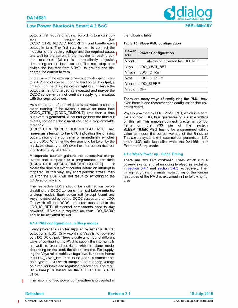
Datasheet Revision 2.1 15-July-2016
CFR0011-120-00-FM Rev 5 37 of 460 © 2016 Dialog Semiconductor
DA14681
Low Power Bluetooth Smart 4.2 SoC PRELIMINARY
outputs that require charging, according to a configur-able sequence (i.e.DCDC_CTRL_0[DCDC_PRIORITY]) and handle eachoutput in turn. The first step is then to connect theinductor to the battery voltage and the required outputand wait for the current in the inductor to reach a cer-tain maximum (which is automatically adjusteddepending on the load current). The next step is toswitch the inductor from VBAT1 to ground and dis-charge the current to zero.
In the case of the external power supply dropping downto 2.4 V, and of course upon the load on each output, atime-out on the charging cycle might occur. Hence theoutput rail is not charged as expected and maybe theDCDC converter cannot continue supplying this outputwith the required power.
As soon as one of the switches is activated, a counterstarts running. If the switch is active for more thanDCDC_CTRL_1[DCDC_TIMEOUT] time then a timeout event is generated. A counter gathers the time outevents, compares the current value to a programmablethreshold(DCDC_CTRL_3[DCDC_TIMEOUT_IRQ_TRIG]) andissues an interrupt to the CPU indicating the phasingout situation of the converter or immediately switchesto the LDOs. Whether the decision is to be taken by thehardware circuitry or SW over the interrupt service rou-tine is user programmable.
A separate counter gathers the successive chargeevents and compared to a programmable threshold(DCDC_CTRL_3[DCDC_TIMEOUT_IRQ_RES] itclears the time out event counter before an interrupt istriggered. In this way, any short periodic stress inter-vals for the DCDC will not result to switching to theLDOs automatically.
The respective LDOs should be switched on beforedisabling the DCDC converter (i.e. just before enteringa sleep mode). Each power rail (except Vcont andVsys) is covered by both a DCDC output and an LDO.To switch off the DCDC, the user must enable theLDO_IO_RETx (if external components need to staypowered). If Vradio is required on, then LDO_RADIOshould be activated as well.
4.1.4 PMU configurations in Sleep modes
Every power line can be supplied by either a DC-DCoutput or an LDO. Only Vcont and Vsys is not poweredby a DC-DC output. There is quite a number of differentways of configuring the PMU to supply the internal railsas well as external devices, while in sleep mode,depending on the load, the sleep time etc. For supply-ing the Vsys rail a stable voltage level is needed hencethe LDO_VBAT_RET has to be used, a sample-and-hold type of LDO which samples the bandgap voltageon a regular basis and regulates accordingly. The regu-lar wake-up is based on the SLEEP_TIMER_REGvalue.
The recommended power configuration is presented in
the following table:
There are many ways of configuring the PMU, how-ever, there is one recommended configuration that cov-ers all cases.
Vsys is powered by LDO_VBAT_RET, which is a sam-ple and hold LDO, thus guaranteeing a stable voltageon this rail. This enables connecting external compo-nents on the V33 pin of the system.SLEEP_TIMER_REG has to be programmed with avalue to trigger the period wakeup of the Bandgap.This covers systems with external components on 1.8Vand/or 3.3V rails kept alive while the DA14681 is inExtended Sleep mode.
4.1.5 Wake/Power up - Sleep Timing
There are two HW controlled FSMs which run atpower/wake up and when going to sleep as explainedin section 3.4.1 and section 3.4.2 respectively. Theirtiming regarding the enabling/disabling of the variousresources of the PMU is explained in the following fig-ures:
Table 10: Sleep PMU configuration
Power Rail
Power Configuration
Vcont always on powered by LDO_RET
Vsys LDO_VBAT_RET
Vflash LDO_IO_RET
Vext LDO_IO_RET2
Vcore LDO_SLEEP
Vradio OFF

Datasheet Revision 2.1 15-July-2016
CFR0011-120-00-FM Rev 5 38 of 460 © 2016 Dialog Semiconductor
DA14681
Low Power Bluetooth Smart 4.2 SoC PRELIMINARY
In the case of powering up the system, the HW FSM asdepicted in Figure 3, enables the various LDOs whilebeing clocked by the RC32K. Each LDO requires a cer-tain amount of time to settle depending on the load ofthe power rail. The LDOs are ready within 12 clockcycles (or 380 us) and then the clock is switched to theRC16 which has not yet been trimmed, hence the fre-quency is near 10 MHz.
In the case of waking up from any of the sleep modes,the HW FSM operates at either the RCX or theXTAL32K clock hence the actual frequency may varyfrom 10.5 kHz to 32,768 kHz. The FSM filters the wakeup event at the first state (an interrupt coming from aGPIO or an internal timer) and then it performs thesame steps as in the power up case. The only differ-ence here is that the amount of time required for theLDOs to settle might be less then before since thesleep time might have been short enough to allow atotal discharge of the capacitances, internally as wellas externally. However, do the frequency variation thewake up time might reach 1.2 ms if the RCX is used.
In both cases, as soon as the RC16 clock is enabled,the FSM hands control to the CPU. The CPU will startexecuting code from address 0x0. If it is a power up,the BootROM code resides at address 0x0. If it is awake up, the RAM is remapped at address 0x0. Theactual application code is responsible for starting theDC-DC controller by settingDCDC_CTRL_0_REG[DCDC_MODE]=Active. Further-more, the respective rails might or might not be ena-
bled by respectively programming theDCDC_<rail>_ENABLE_xV bits.
Preparing the system for any of the sleep modes,requires that the application switches back the clock tothe RC16 and switches off the XTAL16M (see Figure18). After executing the WFI command (which puts thechip into sleep), the clock is switched to the lp_clk(RCX or XTAL32K) the retention LDOs are enabled(LDO_VBAT_RET, LDO_IO_RET and LDO_IO_RET2)and the core (VDD) voltage LDO is disabled so that theLDO_sleep takes over. The actual amount of clockcycles since the WFI is issued up to the point wherethe lp_clk starts and the FSM changes state is 7.Depending on wether a value has been programmed inthe SLEEP_TIMER_REG, the system is automaticallyshorty waken up every so many ticks (lp_clk) to quicklysample the bandgap voltage and get back to sleep.The DC-DC and the LDO_VBAT_RET require a sam-ple-and-hold operation, hence if these two elementsare not part of the sleep strategy, SLEEP_TIMER_REGshould be kept to 0. The overall FSM latency is 4 lp_clkclock cycles
Figure 17: Wake/Power-Up timing and PMU operations
Start V33 Start VDD1V8P Start VDD1V8 Start VDD_CORESwitch
to RC16
CLK
RUNNING SW ...
LDO_VBAT
LDO_CORE
LDO_IO2
LDO_IO
DCDC_1V8
DCDC_1V8P
DCDC_1V2
DCDC_1V4
SLEEP
W ake Up Event
Filter W UP
LDO_IO2_RET
LDO_IO_RET
LDO_VBAT_RET
Wake Up Process
HW controlled
SW controlled
Power Up
W ake Up
HW FSM
XTAL32K(30.5us) / RCX (95.2us)
RC32 (31.2us) RC16 untrimmed (~100ns)
RC16 trimmed (~60ns)
RC16_Enable

Datasheet Revision 2.1 15-July-2016
CFR0011-120-00-FM Rev 5 39 of 460 © 2016 Dialog Semiconductor
DA14681
Low Power Bluetooth Smart 4.2 SoC PRELIMINARY
.
If the SLEEP_TIMER_REG is programmed to wake upthe system for rails charging (DCDC operation) andbandgap sampling, then the timing of the HW FSMlooks as illustrated in Figure 19. The state machine isclocked by the lp_clk and starts with enabling theBandgap. On the next state, it enables the RC16 clock(WPS_CLK) and following that, a sampling of theBrown Out Detection circuit on the various power railoccurs (WPS_BOD). The sampling is performed withthe BOD_clk at 1 MHz (see Figure 27).
Next state is dedicated to the DCDC converter(WPS_SIMO). This is when the charging of the differ-ent power rails will happen if the DCDC is set at sleepmode by programming theDCDC_CTRL_0_REG[DCDC_MODE] flag. During thelast 3 states the sampling and hold of the bandgap volt-age reference occurs, required by theLDO_VBAT_RET, the LDO_IO_RET andLDO_IO_RET2.
Charging of the DCDC rails as well as sample-and-holdfunctionality of the LDOs are both displayed in Figure19 to allow illustrating the waveform for all cases. Inreality, depending on the power configuration, only thepre-defined resources will be part of the intermediatewake up FSM.
Figure 18: Goto Sleep timing and PMU operations
Start LDO_VBAT_RET Disable LDO_VBAT
CLK
SLEEPClock ticks = SLEEP_TIMER
LDO_VBAT
LDO_CORE
LDO_IO
LDO_IO2
DCDC_1V8
DCDC_1V8P
DCDC_1V2
DCDC_1V4
LDO_IO2_RET
LDO_IO_RET
LDO_VBAT_RET
HW FSM
XTAL32K(30.5us) / RCX (95.2us) RC16 trimmed (~60ns)
RUNNING SW...
RC16_Enable
Goto SleepDCDC_MODE=Sleep
HW controlled
SW controlled

Datasheet Revision 2.1 15-July-2016
CFR0011-120-00-FM Rev 5 40 of 460 © 2016 Dialog Semiconductor
DA14681
Low Power Bluetooth Smart 4.2 SoC PRELIMINARY
4.1.6 Charger
The charging circuit operates as a constant current/constant voltage source. The control circuit keeps thecharge voltage or the charge current at the predefinedvalues (whichever of the two is reached first). The val-ues can be changed via registerCHARGER_CTRL1_REG.
The charge control circuit is initially supplied from pinVBUS. The complete charging circuit is powered down,when the VBUS voltage is low for more than 10 ms orby setting bit CHARGER_CTRL1_REG[CHARGE_ON]= 0. In a Li-ion application the charger is also disabled,when the voltage on pin NTC is in the “too hot” or “toocold” region.
Note that, the use of the charger requires P1_4 as apower pin and P1_6 for controlling the NTC if required(as shown in Figure 22).
Pre-Charging and Charging
The Charger is supporting pre-charging and normalcharging as explained in the diagram bellow. Thecharger starts at constant current mode (CC) to get thebattery voltage to the predefined voltage level. It thenswitches to constant voltage mode and continues untilthe current drops below the expected threshold indicat-ing that the Battery has reached the charging limits.
The Charger circuitry supports a large range of currentlevels for pre-charge and charging. If the range iswithin 5 mA and 400 mA, then the respective level hasto be programmed in theCHARGER_CTRL1_REG[CHARGE_CUR] field. If therange of pre-charge currents is between 0.2 mA and 15mA then programming theCHARGER_CTRL2_REG[CHARGER_TEST]=0x6 inaddition to the CHARGER_CTRL1_REG is required.This will divide the current level by ~27 hence producesub-miliamps levels.
The pre-charge and charge state machine as imple-mented in software is presented in the following flowchart:
Figure 19: SLEEP_TIMER based wake up timing
Figure 20: Pre-Charge and Charge Voltage/Current Diagram
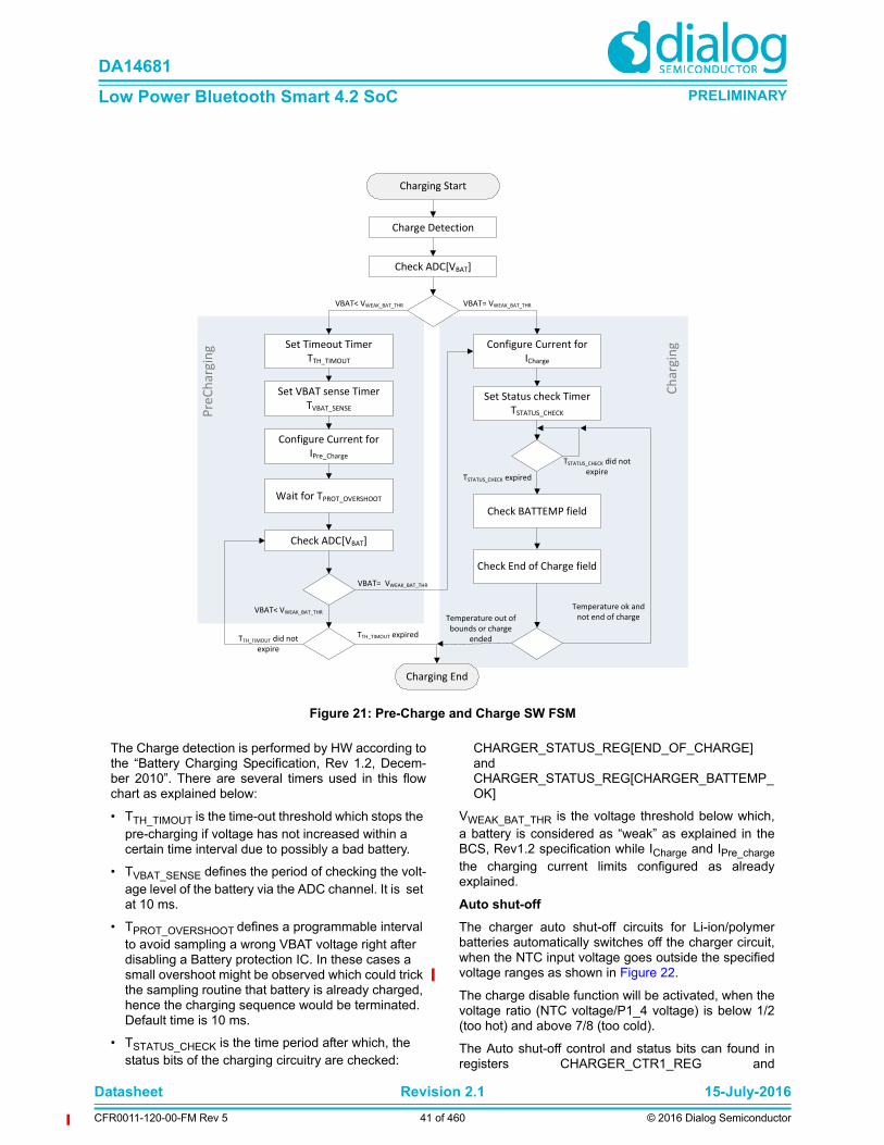
Datasheet Revision 2.1 15-July-2016
CFR0011-120-00-FM Rev 5 41 of 460 © 2016 Dialog Semiconductor
DA14681
Low Power Bluetooth Smart 4.2 SoC PRELIMINARY
The Charge detection is performed by HW according tothe “Battery Charging Specification, Rev 1.2, Decem-ber 2010”. There are several timers used in this flowchart as explained below:
• TTH_TIMOUT is the time-out threshold which stops the pre-charging if voltage has not increased within a certain time interval due to possibly a bad battery.
• TVBAT_SENSE defines the period of checking the volt-age level of the battery via the ADC channel. It is set at 10 ms.
• TPROT_OVERSHOOT defines a programmable interval to avoid sampling a wrong VBAT voltage right after disabling a Battery protection IC. In these cases a small overshoot might be observed which could trick the sampling routine that battery is already charged, hence the charging sequence would be terminated. Default time is 10 ms.
• TSTATUS_CHECK is the time period after which, the status bits of the charging circuitry are checked:
CHARGER_STATUS_REG[END_OF_CHARGE] and CHARGER_STATUS_REG[CHARGER_BATTEMP_OK]
VWEAK_BAT_THR is the voltage threshold below which,a battery is considered as “weak” as explained in theBCS, Rev1.2 specification while ICharge and IPre_chargethe charging current limits configured as alreadyexplained.
Auto shut-off
The charger auto shut-off circuits for Li-ion/polymerbatteries automatically switches off the charger circuit,when the NTC input voltage goes outside the specifiedvoltage ranges as shown in Figure 22.
The charge disable function will be activated, when thevoltage ratio (NTC voltage/P1_4 voltage) is below 1/2(too hot) and above 7/8 (too cold).
The Auto shut-off control and status bits can found inregisters CHARGER_CTR1_REG and
Figure 21: Pre-Charge and Charge SW FSM
Charging Start
Charge Detection
Check ADC[VBAT]
Set Timeout Timer TTH_TIMOUT
VBAT< VWEAK_BAT_THR
Configure Current for ICharge
VBAT= VWEAK_BAT_THR
Set VBAT sense TimerTVBAT_SENSE
Configure Current for IPre_Charge
Check ADC[VBAT]
VBAT< VWEAK_BAT_THR
TTH_TIMOUT expiredTTH_TIMOUT did not expire
Charging End
VBAT= VWEAK_BAT_THR
Check BATTEMP field
Check End of Charge field
Set Status check TimerTSTATUS_CHECK
Temperature out of bounds or charge
ended
TSTATUS_CHECK expired
TSTATUS_CHECK did not expire
Temperature ok and not end of charge
PreCharging
Charging
Wait for TPROT_OVERSHOOT

Datasheet Revision 2.1 15-July-2016
CFR0011-120-00-FM Rev 5 42 of 460 © 2016 Dialog Semiconductor
DA14681
Low Power Bluetooth Smart 4.2 SoC PRELIMINARY
CHARGER_STATUS_REG.
R1 can be dimensioned as follows:
R1 = RNTC@Tcritical
E.g. if the NTC is 4.7 kat Tcritical = ~40 °C, R1 mustalso be 4.7 k, charging will stop at the “too hot” limit.The “too cold” temperature is not critical and will inpractice be around 0 °C.
If the NTC auto shut-off feature is not required, bitCHARGER_CTR1_REG[NTC_DISABLE] must be setto ‘1’.
End Of Charge detection
This is an indicator when the charge current isdecreased to 10% of the programmed value and canbe read atCHARGER_STATUS_REG[END_OF_CHARGE]. The
charge cycle is not affected directly. This indicator canbe used by higher-level control to manipulate thecharge process.
Cold battery protection can be switched-off indepen-dently from the NTC_DISABLE control.
Non-rechargeable batteries
A 3.74 V charge level is provided to test for non-rechargeable NiMH batteries. For two NiMH batteriesthe maximum charging voltage is expected to be 3.4 V.When 3.74 V is selected and an ADC measurementindicates a quick rise above the 3.4 V level, most likelynon-rechargeable batteries are present and thecharger must be disabled.
4.1.7 Fuel gauge
The Fuel Gauge, State of Charge (SOC) circuit is usedto accurately determine the actual amount of charge(Coulombs) in rechargeable batteries as well as thedischarge state of non-rechargeable batteries. Thisinformation can be used as battery status indication tothe user.
Features
• Coulomb Counter fuel gauge with high accuracy Sigma delta ADC 0.05% at 1A Max
• Integrates charge and discharge currents
• Measures average currents
• Offset cancelling by chopper amplifier
• Power saving mode with auto increment
Figure 22: Charger auto shut-off circuit
NTC(10k)
R1(10k)
Too Cold
Temperature ok
Too Hot
1
7/8
1/2
GND
NTC/P1_6
CHARGE Disable
NTC_DISABLE
7/8*VDD
1/2*VDD
+
+
‐
‐
P1_4
NTC_LOW_DISABLE

Datasheet Revision 2.1 15-July-2016
CFR0011-120-00-FM Rev 5 43 of 460 © 2016 Dialog Semiconductor
DA14681
Low Power Bluetooth Smart 4.2 SoC PRELIMINARY
Architecture
The Fuel Gauge measures integrates the currentthrough the battery by measuring the voltage over a0.1 (typical) external resistor or PCB wire usingSOCp and SOCn pins. Recommended settings will bebased on this resistor value.
During operation (charge or discharge) the SOC con-tinuously integrates the voltage on SOCn/SOCp usinga Sigma Delta ADC and integrating counter which is
the time base for the 40 bits Fuel Gauge up/downcounter. The chopper amplifier cancels any offsetbefore passing it to the SD ADC. The integrated valueis read via the SOC_CHARGE_CNTRx_REG (x=1,2,3)and the average current via the 16 bitsSOC_CHARGE_AVG_REG (9 bit + sign + fractional).
All SOC_* registers can be read out via APB16 inter-face.
Operation (rechargeable battery)
Figure 24 shows the Fuel Gauge Hardware/Softwareoperation. The SOC_CHARGE_CNTRx_REG repre-sents the actual amount of charge Q = I*t added orsubtracted from the battery after the counter is resetwith SOC_CTRL1_REG[SOC_RESET_CHARGE].
With the battery charger enabled, a fully charged bat-tery will set bitCHARGER_STATUS_REG[END_OF_CHARGE]. Atthis point the SOC counter can be reset, starting tocount down as soon as the battery is removed from thecharger. A local variable “full_charge” is determinedbased on the battery capacity, aging and temperatureparameters. The actual battery voltage is determinedfrom a VBAT voltage measurement using the generalpurpose ADC. At the lowest operational battery level,the SOC_CHARGE_CNTRx_REG represents the bat-tery capacity which will be negative at this point. TheCurrent charge = full_charge - SOC counter value.
Reversely, if the counter is reset at the lowest batteryvoltage, the increasing counter represents the currentactual battery charge.
At insertion of a new battery the MIN/MAX values ofthe counter are unknown, so the above described cali-bration procedure must be repeated.
Power saving mode
For power saving the SOC analog part can be disabledand the SOC_ADD2CH_REG will be used to decre-ment the SOC_CHARGE_CNTRx_REG at the defaultsample frequency of 1 MHz. The value of theSOC_ADD2CH_REG can be determined from theSOC_CHARGE_AVG_REG when not in power saving.
Figure 23: State of charge (SOC) circuit block diagram
Chopperstage
SOCp
SOCn
Star-point connection
SD ADC(fs=1MHz)
SD Counter
SOC_CHARGE_CNTRx_REG
SOC_CHARGE_AVG_REG
(Fuel Gauge)
(Average current)
VBAT
APB16
SOC_CTRLx_REG
DIVNX_CLK
0.1Ohm
SOC_ADD2CH_REG
SOC_RESET_CHARGE

Datasheet Revision 2.1 15-July-2016
CFR0011-120-00-FM Rev 5 44 of 460 © 2016 Dialog Semiconductor
DA14681
Low Power Bluetooth Smart 4.2 SoC PRELIMINARY
4.1.8 USB charger detection
The USB controller has built-in hardware to determinethe charger type to which it is connected. Dependingon the charger type, battery state and USB connectionstate a defined current can be drawn from the charger.
Features
• Complies to “Battery Charging Specification”Revision V1.2 December 7, 2010 (BC1.2)
• Charger type detection: Dedicated Charging Port (DCP), Charging Downstream Port (CDP), Standard Downstream Port, PS2 port and Proprietary charger
• Dead battery provision
• Compatible with various smartphone chargers
Figure 24: Fuel Gauge operation
current_charge
SOC_CHARGE_CNTRx_REG
SOC_ADD2CH_REG
full_charge
Used in power saving mode. Represents charge when
SOC Analog is off
Battery capacity
Aging & temperature
compensation
add
CHARGER_STATUS_REG[END_OF_CHARGE] ==1
SOC_CTRL1_REG[SOC_RESET_CHARGE] =1
SOC Analog ++/--
++/--
SOC_CHARGE_AVG_REGMeasure once at low current
when not in power saving modeHW
SW
Figure 25: USB charger detection block diagram (BC1.2)
<0.25 V -> 0>0.4 V -> 1
RDM_DWN
IDP_SRC
IDP_SRC_ONVDP_SRC_ON
USB_CHG_DET
USBP
USBN
VBUS
VSS
Receptacle
(10 A)
(15k)
<0.25 V -> 0>0.4 V -> 1
USB_DCP_DET
IDM_SINK_ON
<0.8 V -> 0>1.5 V -> 1
USB_DM_VAL
(100 A)
IDP_SINK_ON
VDM_SRC_ON
(0.6 V)
<0.8 V -> 0>1.5 V -> 1
USB_DP_VAL
+
VDP_SRC_ON
VDM_SRC_ON
VBUS
D+
D-
GND GND
VBUSCharger
CHARGE_STS

Datasheet Revision 2.1 15-July-2016
CFR0011-120-00-FM Rev 5 45 of 460 © 2016 Dialog Semiconductor
DA14681
Low Power Bluetooth Smart 4.2 SoC PRELIMINARY
The USB interface supports the battery charging withthe following hardware blocks as shown in Figure 25.
• A voltage source of 0.6 V can be switched to USBP or USBN with USB_CHARGER_CTRL_REG bits VDP_SRC_ON resp. VDM_SRC_ON.
• A current sink of 100 A can be switched to USBP or USBN with USB_CHARGER_CTRL_REG bits IDP_SINK_ON resp. IDM_SINK_ON. (Note that internal logic prevents to both switches can be ena-ble at the same time)
• A current source IDP_SRC and RDM_DWN can be ena-bled with USB_CHARGER_CTRL_REG[IDP_SRC_ON]
• A logic level Schmitt trigger for USBN, USBP read in USB_CHARGER_STAT_REG bitsUSB_DM_VAL, resp. USB_DP_VAL logic level(0: <0.8 V 1: >2 V)
• A comparator output CHG_DET read in USB_CHARGER_STAT_REG[USB_CHG_DET] to detect a level of 0.4 V < USBN < 1.5 V to indicate that a DCP or CDP is connected.
• A comparator output DCP_DET read inUSB_CHARGER_STAT_REG[USB_DCP_DET] to detect a level of 0.4 V < USBP < 1.5 V to indicate that a DCP is connected.
Initially all bits of USB_CHARGER_CTRL_REG mustbe set to reset value ‘0’.
The presence of VBUS can be checked by reading bitBAT_STATUS_REG[VBUS_AVAILABLE].
Optionally, in case the receptacle's VBUS is connectedto the CHARGE pin via a resistor, bitBAT_STATUS_REG[CHARGE_STS] is set whenVcharge > Vih_charge (1.5 V). This value meets theVOTG_SESS_VLD value. With the keyboard interfaceconfigured to detect a level change of the CHARGEpin, bit KEY_STATUS_REG[0] is set and a KEYB_INTis generated. Optionally, an accurate value of VBUScan be determined with a resistor divider on VBUS toVSS, connected to one of the general purpose ADCinputs.
Detection negotiation
When a downstream port drops VBUS, the bus will dis-charge and BAT_STATUS_REG[VBUS_AVAILABLE]goes to 0. In case VBAT supplies the CHARGE pin aKEYB_INT interrupt can be generated to restart thedetection sequence.
Contact detection
If USB_CHARGER_CTRL_REG[IDP_SRC_ON] is set,bit USB_CHARGER_STAT_REG[USB_DP_VAL] indi-cates that the data pins make contact (see Table 11).
It is the responsibility of the SW to wait until the USBNand USBP contact bouncing has finished before theregister is read.
Primary charger detection
Primary charger detection is used to detect whetherthe downstream port has charging capabilities or not.The detection is initiated by setting bitsUSB_CHARGER_CTRL_REG[VDP_SRC_ON] andUSB_CHARGER_CTRL_REG[IDM_SINK_ON]. Thisenables the voltage source VDP_SRC on USBP and thecurrent source IDM_SINK on USBN. The measured lev-els on USBP and USBN shown in Table 12 determinethe value of bitUSB_CHARGER_STAT_REG[USB_CHG_DET].
Note 1: After 20 ms a valid comparator signal is found, after 40 ms
the comparator signal can be read in USB_CHG_DET.
Note that when the charger detection is done beforethe charging downstream port is enabled its VDM_SRC(so before 20 ms) a standard downstream port isdetected, which is safe but incorrect. After theVDM_SRC has been enabled in the charging down-stream port, a charger port is detected.
Table 11: USBP, USBN contact detection
Port USBP USBN USB_DP_VAL
Nothingconnected
>1.5 V 0 1
Standard down-stream
<0.8 V 0 0
Dedicated charger
<0.8 V <0.8 V 0
Charging down-stream
<0 .8 V <0.8 V 0
Table 12: Charger type detection
Port USBP USBN USB_CHG_DET
Dedicated charger
0.6 V >0.4 V<1.5 V
1
Charging down-stream
0.6 V First <0.25 V Then 0.6 V
0 (Note 1)then 1 after1 ms to 20 ms
Standard down-stream
0.6 V <0.25 V 0
PS2 2 V 2 V 0

Datasheet Revision 2.1 15-July-2016
CFR0011-120-00-FM Rev 5 46 of 460 © 2016 Dialog Semiconductor
DA14681
Low Power Bluetooth Smart 4.2 SoC PRELIMINARY
Secondary charger detection
Secondary charger detection can be used to distin-guish a dedicated charger or a charging downstreamport. The detection is initiated by setting bitsUSB_CHARGER_CTRL_REG[VDM_SRC_ON] andUSB_CHARGER_CTRL_REG[IDP_SINK_ON]. Thisenables VDM_SRC and IDP_SINK. The differencebetween a DCP and a CDP is shown Table 13..
Finally VDP_SRC shall be enabled as defined in theGood Battery Algorithm.
Interrupts
The charger detection hardware can operate in pollingmode or can generate a USB interrupt to the ARM Cor-
texTM M0. A change in one of the bits [3:0] of registerUSB_CHARGER_STAT_REG, sets bitsUSB_MAEV_REG[USB_CH_EV] if the correspondingbits [7:4] are set to ‘1’. If USB_CHARGER_STAT_REGis read, bit USB_CH_EV interrupt is cleared. The inter-rupt “set” conditions have priority over the “clear” condi-tion of the read access.
Once VBUS is inserted, CHARGE generates aKEYB_INT. A debounce timer for Contact Detectionand wait time to detect a standard downstream portmust be done by software polling or by using systemtimer interrupts SWTIM_INT.
USB V1.1 compatibility
In USB V1.1 the integrated USBP and USBN resistorswere used for a dedicated charger detection. Althoughnot very convenient, these resistors can still be used toforce High/Low levels on the USB lines.
Smartphone charger detection
The battery charger detection circuit is able to detectsmartphone chargers with characteristics shown inTable 14.
Table 13: Secondary charger detection
Port USBP USBN USB_DCP_DET
Dedicated charger
>0.4 V<1.5 V
0.6 V 1
Charging down-stream
<0.25 V 0.6 V 0
Table 14: Smartphone charger characteristics
USBP USBN Load current
2.0 V 2.0 V up to 500 mA
2.0 V 2.8 V up to 1 A
2.8 V 2.0 V up to 2 A
2.8 V 2.8 V Not defined
Table 15: Smartphone charger detection
USBP/USBN
USB_DP_VAL /USB_DM_VAL
USB_DP_VAL2 /USB_DM_VAL2 Voltage
2 V 1 0 >1.5 V<2.3 V
2.8 V 1 1 >2.5 V

Datasheet Revision 2.1 15-July-2016
CFR0011-120-00-FM Rev 5 47 of 460 © 2016 Dialog Semiconductor
DA14681
Low Power Bluetooth Smart 4.2 SoC PRELIMINARY
5 ResetThe DA14681 comprises an RST pad which is activeHIGH. It contains an RC filter for spike suppression. Italso contains a 25 k pull-down resistor. The typicallatency of the RST pad is in the range of 2 s.
Furthermore, a separate programmable Brown-Outblock will issue a Power On Reset (POR) upon voltagereaching the minimum threshold on each of the threemain power rails of the system.
Features
• RC spike filter on RST to suppress external spikes (400 k2.8 pF)
• Three different reset lines (SW, HW and POR)
• Power On Reset (POR) issued if voltage threshold reached on VDD, VDD1v8 or V33 rails
• Programmable POR voltage threshold for the VDD rail in sleep (0.7V or 0.8V)
• Configurable POR enables for the VDD1v8 and the VDD3v3 rails
5.1 POR, HW AND SW RESET
The Power On Reset (POR) signal is generated inter-nally and will release the system’s flip-flops as soon asthe VDD voltage crosses the minimum threshold valuewhich at 0.6mV and the Brown-Out Detection FSMsenses the various internal voltage levels to be higherthan the programmed thresholds as explained in sec-tion 5.2. The POR resets everything in the chip.
There are two other main reset signals in the DA14681,namely:
• the HW reset which is basically triggered by the RST pad, the Watchdog expiration, the POR and the debugger (by writting SWD_RESTET_REG)
• the SW reset which is triggered by application soft-ware, writing the SYS_CTRL_REG[SW_RESET] bit, the HW reset, and a special ARM command.
The HW reset can also be automatically activated uponwaking up of the system from an Extended Sleep orDeep Sleep mode by programming bitPMU_CTRL_REG[RESET_ON_WAKEUP]. The HWreset will basically run the cold startup sequence andthe BootROM code will be executed.
The SW reset is the logical OR of a signal from theARM CPU (triggered by writing SCB -> AIRCR =0x05FA0004) and the SYS_CTRL_REG[SW_RESET]bit. This is mainly used to reboot the system after thebase address has been remapped.
Figure 26: Reset and Brown-Out block diagram
ARM
SYS_CTRL_REG[SW_RESET]SWD_RESET_REG
[SWD_HW_RESET_REQ]
Debugger
APB16
25k WATCHDOG
WDOG_reset
NMI
HW_RESETRST
AIRCR[SYSRESETREQ]
SWDIOSWDCLK
AHB32
SWDAP
HW_RESET
(Only Debuggercan set this bit)
POR_RESET
DEBUGGER_ENABLE
PAD_RESET
SW_RESET
Brown Out Detection FSM
BOD_CTRL_REG BOD_CLK
Digital DomainVDD level sense

Datasheet Revision 2.1 15-July-2016
CFR0011-120-00-FM Rev 5 48 of 460 © 2016 Dialog Semiconductor
DA14681
Low Power Bluetooth Smart 4.2 SoC PRELIMINARY
All registers are reset by POR, a few are not reset bythe HW reset signal, and even more are not reset bythe SW reset. These registers are listed in the following
table:
5.2 BROWN OUT DETECTION
The DA14681 contains a brown out detection circuitrywhich is based on sensing selected voltages in the chipevery clock cycle. If one of the voltages is found to bebelow the pre-configured threshold, then a POR isissued.
The BOD FSM is running on the BOD_clk which is 1MHz coming from a fixed division of the RC16 clock by16. The pulses generated for moving from one state toanother are 25% duty cycled, hence 250 kHz.
The threshold values for the comparison are config-ured in the BOD_CTRL_REG. Issuing a POR uponsensing a lower voltage than the pre-defined thresholdis controlled byBOD_CTRL2_REG[BOD_RESET_EN]. Furthermore,each sensed voltage can be masked out with use ofthe BOD_CTRL2_REG enable bits. The FSM steps arethe following:
1. BOD_IDLE: idle state. It will proceed to the nextstate when the system wakes up.
2. BOD_VDD: senses the VDD voltage. it will issuea HW reset if the respective bits are set.
3. BOD_V18: senses the VDD1V8 voltage. it willissue a HW reset if the respective bits are set.
4. BOD_V18P: senses the VDD1V8P voltage. itwill issue a HW reset if the respective bits areset.
5. BOD_V33: senses the V33 voltage. it will issuea HW reset if the respective bits are set.
6. BOD_VBAT: senses the VBAT1 voltage. it willnot issue a HW reset. Instead, it will trigger theDCDC_IRQ line as soon as the VBAT1 voltagereaches 2.45V. The reason is to notify SW thatfrom this point and below, DCDC is not providingbetter efficiency than the LDOs, hence SWshould switch the PMU operation to theLDO_VBAT.
7. BOD_READY: The RC16 will be turned off dur-ing this state and the state machine is set backto BOD_IDLE.
During the extended sleep mode, the BOD FSM is onlytriggered if the SLEEP_TIMER_REG is programmedwith a specific value different than zero. The timing isexplained in Figure 19 of section 4.
Table 16: Reset signals and registers
Reset by POR only Reset by HW resetReset by writing to the SW_RESET bit only
all DCDC_* registers all QSPIC_* registers The rest of the register file
BANDGAP_REG all PLL_* registers
AON_SPARE_REG all CACHE_* registers except for CACHE_MRM_* registers
SYS_STAT_REG All other OTPC_* registers
ANA_STATUS_REG BLE_CNTL2_REG
BOD_STATUS_REG DEBUG_REG. DEBUGS_FREEZE_EN
OTPC_MODE_REG.MODEOTPC_NWORDS_REGOTPC_TIM1_REGOTPC_TIM2_REG
CLK_AMBA_REG[12:0]CLK_FREQ_TRIM_REGCLK_RADIO_REGCLK_CTRL_REGPMU_CTRL_REGSYS_CTRL_REGCLK_32K_REGCLK_16M_REGCLK_RCX32K_REGTRIM_CTRL_REGBOD_CTRL_REGBOD_CTRL2_REGLDO_CTRL1_REGLDO_CTRL2_REGSLEEP_TIMER_REGPOWER_CTRL_REG

Datasheet Revision 2.1 15-July-2016
CFR0011-120-00-FM Rev 5 49 of 460 © 2016 Dialog Semiconductor
DA14681
Low Power Bluetooth Smart 4.2 SoC PRELIMINARY
6 Clock generation 6.1 CLOCK TREE
The generation of the system’s clocks is described in detail in the following figure:
Figure 27: Clock tree diagram
XTALOSC16M
RC16M OSC
2
31
0
PLL96M
CLK_CTRL_REG[SYS_CLK_SEL]
RC32K OSC
RCXOSC
XTAL32K OSC
0
1
2
CLK_CTRL_REG[CLK32K_SOURCE]
3
RF_ADC_div
ahb_clk
sys_clk
DivN
Analog PHY
Digital PHY/ Coex
BLE Core
USB Controller
Divide byBLE_DIV
CLK_RADIO_REG[BLE_ENABLE]
Timer0
Timer1
Breath Timer
WDOG Timer
QSPI Controller
PCM/I2S
PDM
SRC
SOC
ADC
I2C/I2C2
SPI/SPI2
QUAD Decoder
KEYB SCAN
IR Generator
TRNG
AES/HASH
ECC
ARM M0
OTP Controller
APB Interfaces
Wake UP
CLK_TMR_REG[TMR2_CLK_SEL]
Timer2
0
1
Divide byTMR2_DIV
CLK_TMR_REG[TMR2_ENABLE]
CLK_TMR_REG[TMR1_CLK_SEL]
0
1
Divide byTMR1_DIV
CLK_TMR_REG[TMR1_ENABLE]
CAPTIM_CTRL_REG[CAPTIM_SYS_CLK_EN]
0
1
TIMER0_CTRL_REG[TIM0_CLK_SEL]
0
1
Divide byTMR0_DIV
CLK_TMR_REG[TMR0_ENABLE]
CLK_TMR_REG[TMR0_ENABLE]
Divide by32 (fixed)
Divide byQSPI_DIV
Divide byPCM_DIV
PCM_DIV_REG[CLK_PCM_EN]
PCM_DIV_REG[PCM_SEC_SEL]
Divide byPDM_DIV
Divide bySRC_DIV
Divide by16 (fixed)
CLK_PER_REG[ADC_SEL_SEL]
0
1
0
1
UART/UART2CLK_PER_REG[UART_ENABLE]
CLK_PER_REG[I2C_CLK_SEL]
0
1
CLK_PER_REG[I2C_ENABLE]
CLK_PER_REG[SPI_CLK_SEL]
CLK_PER_REG[SPI_ENABLE]
0
1
Divide byKBSCN_CLKDIV
CLK_PER_REG[KBSCAN_ENABLE]
CLK_PER_REG[KBSCAN_CLK_SEL]
0
1
Divide bySPI_CLK
Divide byHCLK_DIV
Divide byPCLK_DIV
CLK_AMBA_REG[TRNG_CLK_ENABLE]
CLK_AMBA_REG[AES_CLK_ENABLE]
CLK_AMBA_REG[ECC_CLK_ENABLE]
CLK_PER_REG[QUAD_ENABLE]
CLK_PER_REG[IR_CLK_ENABLE]
CLK_AMBA_REG[OTP_ENABLE]
Controlled by HW.Automatically selects lp_clk when Deep/Sleep Mode activated
Lp_clk
ahb_clk
divN_clk
Automatically adopts the division if PLL or XTAL16M is used.
CLK_RADIO_REG[RFCU_ENABLE]
CLK_AMBA_REG[QSPI_ENABLE]
Divide by 214
0
1CLK_CTRL_REG[RUNNING_AT_32K]
Divide byRFCU_DIV
Divide by2 (fixed)
CLK_CTRL_REG[USB_CLK_SRC]
0
1
0
1Div by2
CLK_CTRL_REG[PLL_DIV2]
DCDC
BODDivide by16 (fixed)
CLK_TMR_REG[TMR0_CLK_SEL]
0
1

Datasheet Revision 2.1 15-July-2016
CFR0011-120-00-FM Rev 5 50 of 460 © 2016 Dialog Semiconductor
DA14681
Low Power Bluetooth Smart 4.2 SoC PRELIMINARY
The diagram depicts the possible clock sources as wellas all different divisions and multiplexing paths towardsthe generation of each block’s clock. Furthermore, therequired registers that have to be programmed are alsodesignated on the same diagram.
There are some main clock lines which are of interest:
• lp_clk (black bold line): this is the low power clock used for the sleep modes and can only be either the RCX, the RC32K or the XTAL32K.
• sys_clk (green line): this is the system clock, used for the AMBA clock (hclk) which runs the CPU the memories and the bus. This clock sources can be any oscillator, the PLL or even an externally supplied digital clock.
• divn_clk (red line): this is a clock which automatically adjusts the division factor on the sys_clk to always generate 16 MHz. This enables the dynamic activa-tion of the PLL to provide more processing power at the CPU, without affecting the operation of blocks designed for 16 MHz.
6.2 CRYSTAL OSCILLATORS
The Digital Controlled Xtal Oscillator (DXCO) is aPierce configured type of oscillator designed for lowpower consumption and high stability. There are twosuch crystal oscillators in the system, one at 16 MHz(XTAL16M) and a second at 32.768 kHz (XTAL32K).The 32.768 kHz oscillator has no trimming capabilitiesand is used as the clock of the Extended/Deep Sleepmodes. The 16 MHz oscillator can be trimmed.
The principle schematic of the two oscillators is shownin Figure 28: below. No external components arerequired other than the crystal itself. If the crystal has acase connection, it is advised to connect the case toground.
6.2.1 Frequency control (16 MHz crystal)
Register CLK_FREQ_TRIM_REG controls the trim-ming of the 16 MHz crystal oscillator. The frequency is
trimmed by two on-chip variable capacitor banks. Bothcapacitor banks are controlled by the same register.
The capacitance of both variable capacitor banks var-ies from minimum to maximum value in 2048 equalsteps. With CLK_FREQ_TRIM_REG = 0x000 the max-imum capacitance and thus the minimum frequency isselected. With CLK_FREQ_TRIM_REG = 0x7FF theminimum capacitance and thus the maximum fre-quency is selected.
The eight least significant bits ofCLK_FREQ_TRIM_REG directly control eight binaryweighted capacitors, as shown in Figure 29. The threemost significant bits are decoded according to Table17. Each of the seven outputs of the decoder controls acapacitor (value is 256 times the value of the smallestcapacitor).
6.2.2 Automated trimming and settling notification
There is provision in the DA14681 for automating theactual trimming of the 16 MHz crystal oscillator. This isa special hardware block that realizes the XTAL trim-ming in a single step. Notification about the XTAL oscil-lator being settled after applying the trim value is also
Figure 28: Crystal oscillator circuits
XTA
L16
Mp
clock16MHz
XTA
L16
Mm16 MHz
XTA
L32
Kp
clock32kHz
XTA
L32
Km32.768 kHz
0-22.4 pF
Figure 29: Frequency trimming
Table 17: CLK_FREQ_TRIM_REG Decoding 3 --> 7
Input[2:0] Output[6:0]
2 1 0 6 5 4 3 2 1 0
0 0 0 0 0 0 0 0 0 1
0 0 1 0 0 0 0 0 0 1
0 1 0 0 0 0 0 0 1 1
0 1 1 0 0 0 0 1 1 1
1 0 0 0 0 0 1 1 1 1
1 0 1 0 0 1 1 1 1 1
1 1 0 0 1 1 1 1 1 1
1 1 1 1 1 1 1 1 1 1
Decoding3 --> 7
01...678910
CLK_FREQ_TRIM_REG
...
...
13 fF27 fF1.6 pF3.2 pF 3.2 pF ...

Datasheet Revision 2.1 15-July-2016
CFR0011-120-00-FM Rev 5 51 of 460 © 2016 Dialog Semiconductor
DA14681
Low Power Bluetooth Smart 4.2 SoC PRELIMINARY
provided in form of an interrupt, namely thextal16rdy_irq line.
The automated mechanism for applying the trim value
and signalling that the oscillator is settled is describedin the following figure:
The XTALRDY_IRQ is always triggered as soon as aninternal counter reaches the value 1 counting downfrom starting value programmed atXTALRDY_CTRL_REG. This counter runs on theRC32 clock if the system is powering up, or the sleepclock if the system is waking up. Enabling of theXTAL16M oscillator is done by HW. There are twointervals until the interrupt notifies the CPU that theXTAL16 can be used:
• The Start-Up, where the XTAL16M oscillator is slowly converging towards the initial frequency of the crystal. This section ends with the application of the trim value to achieve a <50ppm, 16 MHz clock.
• The Settling, where the oscillator settles to the pre-ferred frequency after the application of the trim value
There are two ways of deciding when the start-up sec-tion ends. This decision is controlled byTRIM_CTRL_REG[XTAL_TRIM_SELECT] bitfield:
• Use an analog filter which asserts an internal signal (XTAL16_OK)
• Use a digital counter which counts TRIM_CTRL_REG[XTAL_COUNT_N] number of XTAL16M clocks
In any case, the trim value is applied by HW. At the ris-ing edge of the XTAL16_OK signal, the interrupt coun-
ter current value (XTAL_RDY_CNT) is stored in ashadow register XTALRDY_STAT_REG. Note that, thisregister keeps the previous value and will not be resetunless a HW reset occurs.
The settling section usually takes not more than 5 to 10clock cycles. Using the above, fine tuning and reducingthe XTAL16 settling latency is feasible.
The XTAL16_TRIM_READY bit indicates that the trim-ming process is done. This bit is reset after the XTAL16oscillator is disabled (turning off the system powerdomain) if XTAL_TRIM_SELECT= 00 or 01.
6.3 RC OSCILLATORS
There are 3 RC oscillators in the DA14681: one provid-ing 16 MHz (RC16M), one providing 32 kHz (RC32K)and one providing a frequency in the range of 10.5 kHz(RCX).
The 16 MHz RC oscillator is powered by the DigitalLDO i.e. the VDD = 1.2 V which is available for the corelogic during Active or Sleep Mode. The output clock issignificantly slower than 16 MHz if untrimmed and isused to clock the CPU and the digital part of the chipduring power up or wake up, while the XTAL16M oscil-lator is settling.
The simple RC oscillator (RC32K) operates onVDD = 1.2 V and provides 32 kHz. The main usage ofthe RC32K oscillator is for internal clocking during
Figure 30: Automated mechanism for XTAL16M trim and settling
XTAL_RDY_CNT (8 bits)
On XTAL16_OK rising edge, XTAL_RDY_CNT value is stored here!
Power up: RC32Wake up: LP_CLK
XTAL_RDY_CNT current value
2 1 0
XTAL16MHz
XTAL16M_EN
NXTAL16_CLK_CNT
(10 bits)Counting ... XTAL_COUNT_N‐1
XTAL16RDY_IRQ
0
XTAL16_OK (Analog)
XTALRDY_STAT_REG (8 bits)
XTAL_RDY_CNT old value
HW applies the trim value (TRIM_CTRL_REG) when:‐ either XTAL16_CLK_CNT reaches defined threshold (XTAL_COUNT_N))‐ or XTAL16_OK signal is highThe selection of the mechanism is configurable by XTAL_TRIM_SELECT
XTAL16RDY_IRQ is always asserted when XTAL_RDY_CNT reaches 1
Start Up Time Settling Time
Loads from XTALRDY_CTRL_REG and counting down...

Datasheet Revision 2.1 15-July-2016
CFR0011-120-00-FM Rev 5 52 of 460 © 2016 Dialog Semiconductor
DA14681
Low Power Bluetooth Smart 4.2 SoC PRELIMINARY
power up or startup. It clocks the HW state machinewhich brings up the power management system of thechip.
The enhanced RC oscillator (RCX) provides a stable10.5 kHz. The RCX oscillator can be used to replacethe 32.768 kHz crystal, since it has a precision of< 500 ppm, while its output frequency is quite stableover temperature.
6.3.1 Frequency calibration
The output frequency of the 32 kHz crystal oscillatorand the three RC-oscillators can be measured relativeto the DivN clock using the on-chip reference counter.
The measurement procedure is as follows:
• REF_CNT_VAL = N (the higher N, the more accu-rate and longer the calibration will be)
• CLK_REF_SEL_REG[REF_CLK_SEL] = 0 (RC32K) or CLK_REF_SEL_REG[REF_CLK_SEL] = 1 (RC16M) or CLK_REF_SEL_REG[REF_CLK_SEL] = 2 (XTAL32) or CLK_REF_SEL_REG[REF_CLK_SEL] = 3 (RCX)
• CLK_REF_SEL_REG[REF_CAL_START] = 1 Start the calibration
• Wait until CLK_REF_SEL_REG[REF_CAL_START] = 0
• Read CLK_REF_VAL_H_REG and CLK_REF_VAL_H_REG = M (32-bits values)
• Frequency = (N/M) * 16 MHz
In the case of using the RCX as a sleep clock, the fre-quency calibration should be implemented on eachactive time of a connection interval to guarantee cor-rect operation.
6.4 PLL
This low power PLL multiplies the XTAL16M clock toproduce a 96 MHz clock with 1% precision within a fewus reaching 200 ppm precision in 30 us.
Changing the system’s clock in to the PLL output canbe done dynamically without affecting the operation ofthe chip. Its main purpose is to:
• Provide a divided by 2, 48 MHz required for the operation of the USB Controller
• Provide more processing power to the CPU, ena-bling 80 dMIPS, for computational hungry applica-tions
This PLL dissipates 1.2 mA when operating at 96 MHzwhile the leakage current can reach 1 uA when the PLLis disabled.

Datasheet Revision 2.1 15-July-2016
CFR0011-120-00-FM Rev 5 53 of 460 © 2016 Dialog Semiconductor
DA14681
Low Power Bluetooth Smart 4.2 SoC PRELIMINARY
7 ARM Cortex M0The Cortex-M0 processor is a 32-bit Reduced Instruc-tion Set Computing (RISC) processor with a von Neu-mann architecture (single bus interface). It uses aninstruction set called Thumb, which was first supportedin the ARM7TDMI processor; however, several newerinstructions from the ARMv6 architecture and a fewinstructions from the Thumb-2 technology are alsoincluded. Thumb-2 technology extended the previousThumb instruction set to allow all operations to be car-ried out in one CPU state. The instruction set inThumb-2 includes both 16-bit and 32-bit instructions;most instructions generated by the C compiler use the16-bit instructions, and the 32-bit instructions are usedwhen the 16-bit version cannot carry out the requiredoperations. This results in high code density and
avoids the overhead of switching between two instruc-tion sets.
In total, the Cortex-M0 processor supports only 56base instructions, although some instructions can havemore than one form. Although the instruction set issmall, the Cortex-M0 processor is highly capablebecause the Thumb instruction set is highly optimized.
Academically, the Cortex-M0 processor is classified asload-store architecture, as it has separate instructionsfor reading and writing to memory, and instructions forarithmetic or logical operations that use registers.
A simplified block diagram of the Cortex-M0 is shownin Figure 31.
Features
• Thumb instruction set. Highly efficient, high code density and able to execute all Thumb instructions from the ARM7TDMI processor.
• High performance. Up to 0.9 DMIPS/MHz (Dhrys-tone 2.1) with fast multiplier.
• Built-in Nested Vectored Interrupt Controller (NVIC). This makes interrupt configuration and coding of exception handlers easy. When an interrupt request is taken, the corresponding interrupt handler is exe-cuted automatically without the need to determine the exception vector in software.
• Interrupts can have four different programmable pri-ority levels. The NVIC automatically handles nested interrupts.
• The design is configured to respond to exceptions (e.g. interrupts) as soon as possible (minimum 16 clock cycles).
• Non maskable interrupt (NMI) input for safety critical systems.
• Easy to use and C friendly. There are only two modes (Thread mode and Handler mode). The whole application, including exception handlers, can be written in C without any assembler.
• Built-in System Tick timer for OS support. A 24-bit timer with a dedicated exception type is included in the architecture, which the OS can use as a tick timer or as a general timer in other applications with-out an OS.
• SuperVisor Call (SVC) instruction with a dedicated SVC exception and PendSV (Pendable SuperVisor
Figure 31: ARM Cortex M0 Block Diagram
WakeUp Interrupt Controller(WIC)
Nested Vector Interrupt
Controller(NVIC)
Processor Core
Debug Subsystem
Internal Bus System
Serial-Wire Debug Interface
AHB Lite bus interface unit
Power Management Interface
Connection to Debugger
Memory and Peripherals
Interrupt Request and NMI

Datasheet Revision 2.1 15-July-2016
CFR0011-120-00-FM Rev 5 54 of 460 © 2016 Dialog Semiconductor
DA14681
Low Power Bluetooth Smart 4.2 SoC PRELIMINARY
service) to support various operations in an embed-ded OS.
• Architecturally defined sleep modes and instructions to enter sleep. The sleep features allow power con-sumption to be reduced dramatically. Defining sleep modes as an architectural feature makes porting of software easier because sleep is entered by a spe-cific instruction rather than implementation defined control registers.
• Fault handling exception to catch various sources of errors in the system.
• Support for 32 interrupts.
• Little endian memory support.
• Wake up Interrupt Controller (WIC) to allow the pro-cessor to be powered down during sleep, while still allowing interrupt sources to wake up the system.
• Halt mode debug. Allows the processor activity to stop completely so that register values can be accessed and modified. No overhead in code size and stack memory size.
• CoreSight technology. Allows memories and periph-erals to be accessed from the debugger without halt-ing the processor.
• Supports Serial Wire Debug (SWD) connections. The serial wire debug protocol can handle the same debug features as the JTAG, but it only requires two wires and is already supported by a number of debug solutions from various tools vendors.
• Four (4) hardware breakpoints and two (2) watch points.
• Breakpoint instruction support for an unlimited num-ber of software breakpoints.
• Programmer’s model similar to the ARM7TDMI pro-cessor. Most existing Thumb code for the ARM7TDMI processor can be reused. This also makes it easy for ARM7TDMI users, as there is no need to learn a new instruction set.
7.1 SYSTEM TIMER (SYSTICK)
The Cortex-M0 System Timer (SysTick) can be config-ured for using 2 different clocks. The SysTick Control &Status (STCSR) register specifies which clock shouldbe used by the counter.
STCSR[CLKSOURCE]=0; use the (fixed) external ref-erence clock STCLKEN of 1 MHz.
STCSR[CLKSOURCE]=1; use the (HCLK_DIVdependent) processor clock SCLK (e.g. 2, 4, 8 or 16MHz).
The default SysTick Timer configuration will be usingthe (fixed) external reference clock STCLKEN(STCSR[CLKSOURCE]=0). When necessary, higherclock frequencies can be used with STCSR[CLK-SOURCE]=1 but the software should take theHCLK_DIV dependent core clock SCLK into accountw.r.t. the timing.
7.2 WAKEUP INTERRUPT CONTROLLER
The Wakeup Interrupt Controller (WIC) is a peripheralthat can detect an interrupt and wake the processorfrom deep sleep mode. The WIC is enabled only whenthe DEEPSLEEP bit in the SCR is set to 1 (see SystemControl Register on page 4-16 of the Cortex-M0 UserGuide Reference Material).
The WIC is not programmable, and does not have anyregisters or user interface. It operates entirely fromhardware signals. When the WIC is enabled and theprocessor enters deep sleep mode, the power man-agement unit in the system can power down most ofthe Cortex-M0 processor. This has the side effect ofstopping the SysTick timer. When the WIC receives aninterrupt, it takes a number of clock cycles to wakeupthe processor and restore its state, before it can pro-cess the interrupt. This means interrupt latency isincreased in Deep Sleep mode.
7.3 REFERENCE
For more information on the ARM Cortex M0, see a.o.the ARM documents listed in Table 18.
Table 18: ARM documents list
Document title ARM Document number
1 Cortex™-M0 User Guide Reference Material ARM DUI 0467B (available on the ARM website)
2 Cortex™-M0 r0p0 Technical Reference Manual ARM DDI 0432C (available on the ARM website)
3 ARMv6-M Architecture Reference Manual ARM DDI 0419C (can be downloaded by registered ARM customers)

Datasheet Revision 2.1 15-July-2016
CFR0011-120-00-FM Rev 5 55 of 460 © 2016 Dialog Semiconductor
DA14681
Low Power Bluetooth Smart 4.2 SoC PRELIMINARY
7.4 INTERRUPTS
This section lists all 32 interrupt lines, except the NMIinterrupt, and describes their source and functionality.The overview of the interrupts is illustrated in the fol-lowing table:
Table 19: Interrupt list
IRQ number (inherent priority)
IRQ name Description
0 ble_wakeup_lp_irq Wakeup from Extended Sleep by BLE
1 ble_gen_irq BLE Interrupt. Sources:- finergtim_irq: Fine Target Timer interrupt generated when Fine Target timer expired. Timer resolution is 625μs base time reference- grosstgtim_irq: Gross Target Timer interrupt generated when Gross Tar-get timer expired. Timer resolution is 16 times 625μs base time reference- cscnt_irq: 625μs base time reference interrupt, available in active modes- slp_irq: End of Sleep mode interrupt- error_irq: Error interrupt, generated when undesired behavior or bad programming occurs in the BLE Core- rx_irq: Receipt interrupt at the end of each received packets- event_irq: End of Advertising / Scanning / Connection events interrupt- crypt_irq: Encryption / Decryption interrupt, generated either when AES and/or CCM processing is finished- sw_irq: SW triggered interrupt, generated on SW request
2 RESERVED
3 RESERVED
4 rfcal_irq RF Calibration Interrupt. Generated by the DPHY.
5 RESERVED
6 crypto_irq Crypto interrupt. Sources:- aes_hash_irq: AES or HASH function interrupt.- ecc_irq: Elliptic Curve interrupt.
7 mrm_irq Cache Miss Rate Monitor interrupt.
8 uart_irq uart interrupt.
9 uart2_irq uart2 interrupt.
10 i2c_irq I2C interrupt.
11 i2c2_irq I2C2 interrupt.
12 spi_irq SPI interrupt.
13 spi2_irq SPI2 interrupt.
14 adc_irq ADC interrupt.
15 keybrd_irq Keyboard scanner interrupt.
16 irgen_irq IR generator interrupt.
17 wkup_gpio_irq Wakeup or GPIO interrupt. Will be triggered in Deep Sleep or Hibernation modes (clock-less).
18 swtim0_irq Timer0 interrupt.
19 swtim1_irq Timer1 interrupt.
20 quadec_irq Quadrature decoder interrupt.
21 usb_irq USB controller interrupt.
22 pcm_irq PCM interrupt.
23 src_in_irq Sample rate converter input interrupt.

Datasheet Revision 2.1 15-July-2016
CFR0011-120-00-FM Rev 5 56 of 460 © 2016 Dialog Semiconductor
DA14681
Low Power Bluetooth Smart 4.2 SoC PRELIMINARY
Interrupt priorities are programmable by the ARM Cor-tex M0. The lower the priority number, the higher thepriority level. The priority level is stored in a byte-wideregister, which is set to 0x0 at reset. Interrupts with thesame priority level follow a fixed priority order using theinterrupt number listed in Table 19 (lower interruptnumber has higher priority level).
To access the Cortex-M0 NVIC registers, CMSIS func-tions can be used. The input parameter IRQn of theCMSIS NVIC access functions is the IRQ number. Thiscan be the IRQ number or (more convenient) the corre-sponding IRQ name listed in Table 19. The corre-sponding interrupt handler name in the vector table forIRQ#15 is e.g. UART_Handler. For more informationon the ARM Cortex M0 interrupts and the correspond-ing CMSIS functions, see a.o. section 4.2 Nested Vec-tored Interrupt Controller on pag. 4-3 in the Cortex™-M0 User Guide Reference Material.
The Watchdog interrupt is connected to the NMI inputof the processor.
24 src_out_irq Sample rate converter output interrupt.
25 vbus_irq VBUS presence interrupt. This interrupt requires a clock to be generated. It will not be issued in clock-less power modes.
26 dma_irq DMA interrupt.
27 rf_diag_irq Baseband or Radio diagnostics Interrupt.
28 trng_irq True random number generator interrupt.
29 dcdc_irq DCDC timeout interrupt.
30 xtal16rdy_irq XTAL16 oscillator ready interrupt. Clock is 16MHz (<50ppm) and 60/40 % duty cycle
31 RESERVED
Table 19: Interrupt list
IRQ number (inherent priority)
IRQ name Description
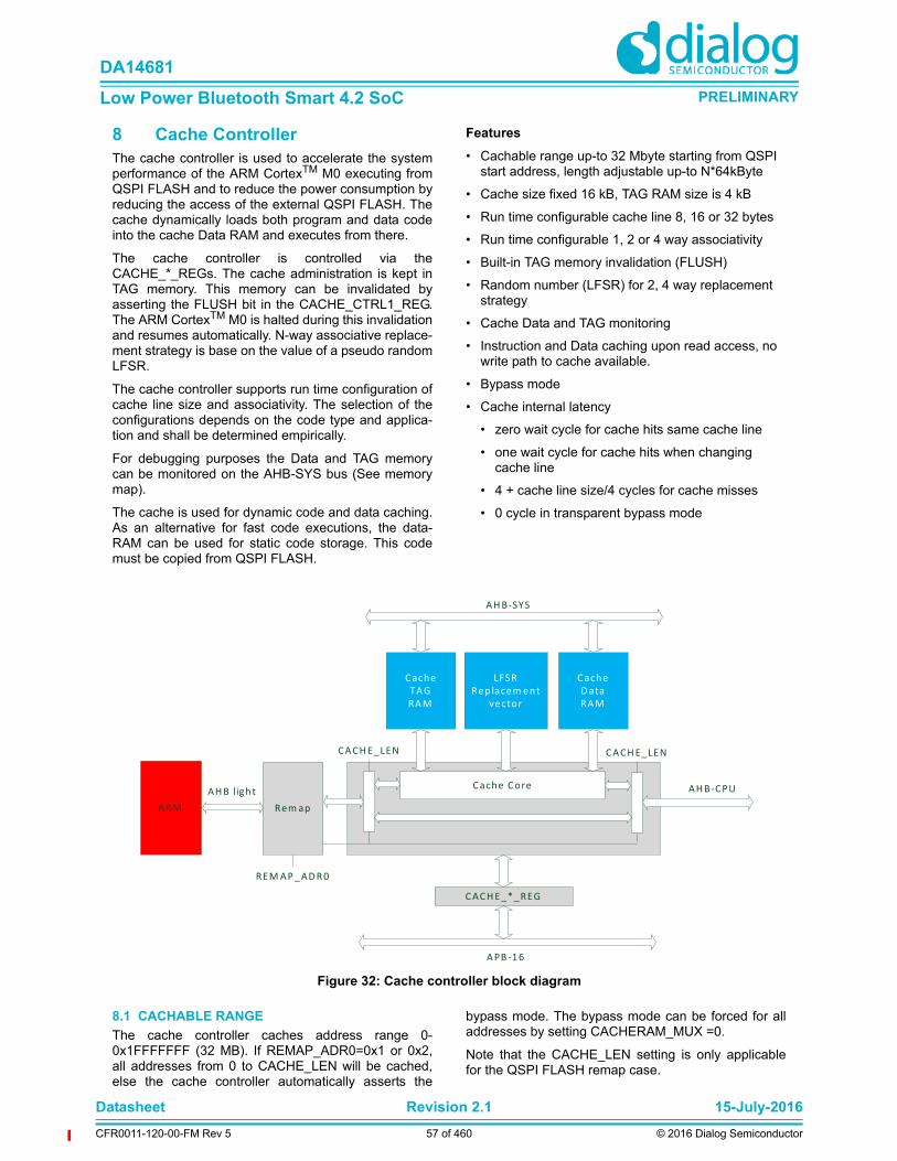
Datasheet Revision 2.1 15-July-2016
CFR0011-120-00-FM Rev 5 57 of 460 © 2016 Dialog Semiconductor
DA14681
Low Power Bluetooth Smart 4.2 SoC PRELIMINARY
8 Cache ControllerThe cache controller is used to accelerate the systemperformance of the ARM CortexTM M0 executing fromQSPI FLASH and to reduce the power consumption byreducing the access of the external QSPI FLASH. Thecache dynamically loads both program and data codeinto the cache Data RAM and executes from there.
The cache controller is controlled via theCACHE_*_REGs. The cache administration is kept inTAG memory. This memory can be invalidated byasserting the FLUSH bit in the CACHE_CTRL1_REG.The ARM CortexTM M0 is halted during this invalidationand resumes automatically. N-way associative replace-ment strategy is base on the value of a pseudo randomLFSR.
The cache controller supports run time configuration ofcache line size and associativity. The selection of theconfigurations depends on the code type and applica-tion and shall be determined empirically.
For debugging purposes the Data and TAG memorycan be monitored on the AHB-SYS bus (See memorymap).
The cache is used for dynamic code and data caching.As an alternative for fast code executions, the data-RAM can be used for static code storage. This codemust be copied from QSPI FLASH.
Features
• Cachable range up-to 32 Mbyte starting from QSPI start address, length adjustable up-to N*64kByte
• Cache size fixed 16 kB, TAG RAM size is 4 kB
• Run time configurable cache line 8, 16 or 32 bytes
• Run time configurable 1, 2 or 4 way associativity
• Built-in TAG memory invalidation (FLUSH)
• Random number (LFSR) for 2, 4 way replacement strategy
• Cache Data and TAG monitoring
• Instruction and Data caching upon read access, no write path to cache available.
• Bypass mode
• Cache internal latency
• zero wait cycle for cache hits same cache line
• one wait cycle for cache hits when changing cache line
• 4 + cache line size/4 cycles for cache misses
• 0 cycle in transparent bypass mode
8.1 CACHABLE RANGE
The cache controller caches address range 0-0x1FFFFFFF (32 MB). If REMAP_ADR0=0x1 or 0x2,all addresses from 0 to CACHE_LEN will be cached,else the cache controller automatically asserts the
bypass mode. The bypass mode can be forced for alladdresses by setting CACHERAM_MUX =0.
Note that the CACHE_LEN setting is only applicablefor the QSPI FLASH remap case.
Figure 32: Cache controller block diagram
Cache DataRAM
Cache TAGRAM
AHB ‐CPUAHB light
AHB ‐SYS
LFSRRep lacement
vector
CACHE_*_REG
Cache Core
APB ‐16
RemapARM
CACHE_LEN CACHE_LEN
REMAP_ADR0

Datasheet Revision 2.1 15-July-2016
CFR0011-120-00-FM Rev 5 58 of 460 © 2016 Dialog Semiconductor
DA14681
Low Power Bluetooth Smart 4.2 SoC PRELIMINARY
8.2 RUNTIME RECONFIGURATION
Associativity and cache line size of cache can bereconfigured at all time by writing theCACHE_ASSOCCFG_REG orCACHE_LNSIZECFG_REG registers. Reconfigurationis done without wait state and without flushing thecache. All the data available in the cache memory arekept except when the associativity is reduced (4-way ->2-way and 2-way -> 1-way). In that case typically halfof the data are unaccessible.
8.2.1 Cache Line reconfiguration
The dynamic configuration of the cache line size usesa physical line size of 8 bytes. When the cache linesize is defined as 16 bytes or 32 bytes, 2 or 4 physicallines are involved.
Reconfiguration of the cache line occurs only whenlines are replaced. Even if the cache line configurationis set to 32 bytes, cache lines of 16 bytes may remainin the cache memory as explained at the example inTable 20.
8.2.2 TAG memory word
The administration memory word decoding is pre-sented in the following table:
8.2.3 Associativity reconfiguration
To enable associativity reconfiguration, the cachememory is organized into four banks.
Depending on the associativity, the four banks canoperate as 4-way, or be concatenated resulting ineither a 2-way or 1-way cache.
8.3 2 AND 4 WAY REPLACEMENT STRATEGY
The cache controller fills each line of the cache firststarting from way0 to way3. When a line is completelyfull, a new way_x victim is chosen in a pseudo randomway.
When a replacement is required, the cache controllerreads the value generated by a pseudo-random num-ber generated to select which way to replace.
The pseudo-random number generator is realizedusing a Linear Feedback Shift Register (LFSR).
8.4 CACHE RESETS
The cache controller has two reset signals connected:
• The HW_RESET. When this reset is activated, allcache logic and registers are reset to their defaultvalues, while all data in the TAG memories arecleared and all CACHE_*_REG are set to their resetvalues. It takes around 450 AHB cycles to clear thecache TAG memory.
Table 20: Cache line size reconfiguration example
Step1: Cache line size = 16 bytesa. CPU Reads @0x00: MissCache Reads 16 bytes in Block 0 @0x00b. CPU Reads @5010: Miss Cache Reads 16 bytes in Block 5 @0x10
Step 2:Cache line size = 32 bytesa. CPU Reads @0x00: Hitb. CPU Reads @5010: Hitc. CPU Reads @5020: MissCache reads 32 bytes in Block 5 @0x20
Although the configuration is 32 bytes, the lines of 16 bytes remain in the cache. Only new lines are 32 bytes.
Step 3:Cache line size = 32 bytesa. CPU Reads @0x6000: Miss Cache reads 32 bytes in Block 6 @0x00
16-byte cache lines already in the cache are replaced by the 32-byte cache line.
Table 21: TAG memory layout
Bit 23 Bits 22:2 Bits 1:0
0 AHB address
00: invalid cache line01: 8 valid bytes10: 16 valid bytes11: 32 valid bytes

Datasheet Revision 2.1 15-July-2016
CFR0011-120-00-FM Rev 5 59 of 460 © 2016 Dialog Semiconductor
DA14681
Low Power Bluetooth Smart 4.2 SoC PRELIMINARY
If a fetch request occurs during this reset period, therequest will be taken into account at the end of thereset and wait-states will be inserted.
• The SW_RESET. Upon a SW_RESET the cachestate machine and TAG memories are reset, but theCACHE_*_REG are not affected and will remain asprogrammed.
8.5 CACHE MISS RATE MONITOR
The DA14681 incorporates a cache miss monitoringcircuitry which is providing real time information on thenumber of cache misses within a certain amount oftime. Upon reaching a programmable threshold, aninterrupt is issued towards the CPU to take action. TheCPU can dynamically change the cache line size, theassociativity or start the PLL to decrease cache linefetch time and consequently power. It can even apply acombination of the aforementioned techniques toadjust system's parameters accordingly. This blockonly operates while the system is in active mode. Mainfeatures are:
• Up to 10 ms active time interval counter
• Registered amount of cache misses
• Registered amount of cache hits
• Programmable threshold of cache misses upon which, an interrupt is generated
CACHE_MRM_HITS_REG contains the amount ofcache hits and CACHE_MRM_MISSES_REG theamount of misses counted within the time interval pro-grammed at CACHE_MRM_TINT_REG in CPU clockcycles.
8.6 CACHE MISS LATENCY AND POWER
This section describes the amount of time (in clockcycles) required from a cache miss up to the point therequired code/data are fetched back to the CPU andexecution continues.
The cache miss latency (TCML) can be split in the fol-lowing intervals:
TCM2R: Time from the cache miss up to request fromthe QSPI Controller.
TR2QA: Time from request up to actual access start.
TRDFL: Time for reading data from the FLASH.
TCLAT: Time required to get data to the CPU (cachelatency).
The final amount of clock cycles is calculated by thefollowing equation:
TCML=TCM2R+TR2QA+TRDFL+TCLAT
where TRDFL depends on the amount of data requestedand is provided by the following formula:
TRDFL = TCMD+TADDR+TDUM+(NCACHELINE*2)+TPIPE
For example, give a cache line configuration of 16bytes, the amount of clock cycles required to read the
data from the FLASH is:
TRDFL = 2+8+4+(16*2)+1=47 clock cycles.
An overview of the cache miss latency calculation isshown in the following table:
The same calculation applies for the OTP cachedcase:
The TOTP_INIT parameter represents the amount ofcycles required for initiating the burst read of the mem-ory.
Especially in the case of the QSPI FLASH, the amountof cache misses, the latency and the FLASH devicemight affect the power of the application since theFLASH has to be activated for long time intervals.However, it is measured that given a low cache missrate, the average power is not dramatically increased.The following figure illustrates the current overhead asa result of the cache miss rate.
Table 22: QSPI FLASH cache miss latency
Time Interval
Clock Cycles Example
TCM2R 3 3
TR2QA 2 2
TRDFL TCMD+TADDR+TDUM+(NCACHELINE*2)+TPIPE
47
TCLAT 4 4
TCML for 16 bytes cache line (QPI mode)
56
Table 23: OTP cache miss latency
Time Interval
Clock Cycles Example
TCM2R 3 3
TOTP_INIT 2 2
TRDOTP NCACHELINE/4 4
TCLAT 4 4
TCML for 16 bytes cache line 13

Datasheet Revision 2.1 15-July-2016
CFR0011-120-00-FM Rev 5 60 of 460 © 2016 Dialog Semiconductor
DA14681
Low Power Bluetooth Smart 4.2 SoC PRELIMINARY
The average increase on an application using aFLASH device powered by the VDD1V8 pin (1.8V),with 5mA read current, is becoming visible (i.e. <1mA)if the miss rate exceeds 40%. For applications that areperiodically repeating activities, the expected miss rateshould be <5% hence the power overhead is minimum.
Figure 33: Current dissipation overhead due to cache miss rate (at 3V)

Datasheet Revision 2.1 15-July-2016
CFR0011-120-00-FM Rev 5 61 of 460 © 2016 Dialog Semiconductor
DA14681
Low Power Bluetooth Smart 4.2 SoC PRELIMINARY
9 AMBA BusThe DA14681 is equipped with a multi-layer AMBA buswhich enables parallel data paths between differentmasters and slaves. The bus matrix comprises 2 mainbusses:
• AHB-CPU bus where the Cache, or the CPU can be masters
• AHB-DMA bus where the DMA the OTP Controller and the AES/HASH DMA can be masters
Features
• Enables data transfers from peripherals to memory while executing code from OTP or external QSPI FLASH
• Provides programmable master priority on AHB-CPU bus
• Provides programmable ICM priority for the con-nected Slaves
• Enables AHB access of the CPU at the cache RAM if no cache functionality is required
There are six slaves which are sitting behind intercon-nection multiplexers (ICMs) namely:
• Memory controller which controls the DataRAM and the ROM cells
• QSPI FLASH memory controller and memory
• 16-bit APB peripheral registers
• AHB register files for the rest of the resources as well as the TRNG RAM
• 32-bit APB peripheral registers
• Cache controller which enables AHB access of the CPU at the cache RAM to be used as an extension of the DataRAM in the case of mirrored mode.
Figure 34: AMBA Bus architecture
Ctrl. Data RAM cellsCache
AHB Reg. FilesBLE regCRYPTO regOTPC regPATCH regECC reg
QSPI FLASH(in package)
Mem.Ctrl.IC
M_
S2
Legend:
AHB/APB Master interface.
AHB/APB Slave interface
AHB/APB Bus
AHB Interconnection Matrix (ICM)
AH
B -
CP
U
ARMM0
QSPIC reg
Re-map
Addr0
Re
g
TRNG RAM
Dat
a
Tag
ROM
AES/Hash DMA
DMA
APB-16 Bridge
AP
B-1
6
AON Reg. FilesCRG regWakeUp reg
ICM
_S3
BLE
Periph. Reg. FilesUART regSPI regetc.
Radio Reg. FilesRF regCoex reg
Sys Reg. FilesWDG regDMA regetc.
OTP Mem
HWpatch
ICM
_S
4
APB-32 BridgeAudio Reg. FilesPCM regetc
OTPC
ICM
_S1
OTPC reg
Remap_RAMS
AP
B-3
2
TRNG Reg. File
ECC
ICM
_S
0
ROM Ctrl.
AH
B -
DM
A

Datasheet Revision 2.1 15-July-2016
CFR0011-120-00-FM Rev 5 62 of 460 © 2016 Dialog Semiconductor
DA14681
Low Power Bluetooth Smart 4.2 SoC PRELIMINARY
In the latter case, the ICM_S0 provides a direct accessof the CPU at the cache RAM cell. The Cache RAMcell is always mapped at address 0x20010000. TheTAG RAM is not used during this mode of operation.
The priority on the AHB-DMA busses regarding themaster arbitration is programmable. The following tabledepicts the default priority scheme (1=Highest Priority):
Table 24: AHB-DMA master default priorities
Priority Master
1 OTP Controller DMA
2 AES/HASH DMA
3 Generic DMA

Datasheet Revision 2.1 15-July-2016
CFR0011-120-00-FM Rev 5 63 of 460 © 2016 Dialog Semiconductor
DA14681
Low Power Bluetooth Smart 4.2 SoC PRELIMINARY
10 Memory ControllerThe Memory controller is responsible for the interfaceof the memory cells with the masters of the systemrequesting for access. It comprises an arbiter whichallows for a configurable priority level between the 3main masters of the RAM. The memory controller alsoallows for the actual physical sequence of the RAMcells in a continuous memory space enabling activationof just the required amount of DataRAM thus saving onpower.
Features
• Five different RAM cells with retention capability (one 8 kB, one 24 kB and three 32 kB)
• Full flexibility of re-arranging the first 3 RAM cells in a continuous RAM space starting at 0x7FC0000
• Arbitration between the AHB masters (CPU or DMAs) the BLE core and the ECC
• Retainable configuration of the RAM cells sequence.
The Shuffle_RAM word in the OTP header encodes thesequence of the RAM cells. This is described in the fol-lowing table:
Selecting the appropriate shuffle value, the minimumrequired memory space can be left retained duringsleep modes hence reducing the sleep power dissipa-tion.
The Memory Controller contains an Arbiter which con-
nects to the following busses:
• ICM which multiplexes the CPU or the DMA access. This interface is capable of operating at maximum 96MHz
• BLE Memory I/F: this is a memory interface from the BLE 4.1 Core directly accessing the RAM used as exchange memory (TX/RX descriptors etc.). This interface is always operating at 16MHz.
• ECC Memory I/F: this is a memory interface from the Elliptic Curve Crypto block directly accessing the RAM used as crypto shared memory. This interface is capable of operating at maximum 96MHz.
The Arbiter implements the priority scheme as depictedin the following figure:
Figure 35: Memory Controller Block Diagram and environment
Memory Controller
AH
B -
DM
A
AH
B-
CP
U
DataRAM 18KB
DataRAM 224KB
DataRAM 332KBA
rbite
r
SYS_CTRL_REG[REMAP_RAMS]
BLE 4.1 BLE - AHB
BLE Mem I/F
Sequence Config
DataRAM 432KB
DataRAM 532KB
0x7FD0000
0x7FD8000
ECC ECC Mem I/F
ICM
_S
0
Table 25: DataRAM cells sequence
Value Cell Addess Size (kB)
0x0 DataRAM1 0x7FC0000 8
DataRAM2 0x7FC2000 24
DataRAM3 0x7FC8000 32
0x1 DataRAM2 0x7FC0000 24
DataRAM1 0x7FC6000 8
DataRAM3 0x7FC8000 32
0x2 DataRAM3 0x7FC0000 32
DataRAM1 0x7FC8000 8
DataRAM2 0x7FCA000 24
0x3 DataRAM3 0x7FC0000 32
DataRAM2 0x7FC8000 24
DataRAM1 0x7FCE000 8

Datasheet Revision 2.1 15-July-2016
CFR0011-120-00-FM Rev 5 64 of 460 © 2016 Dialog Semiconductor
DA14681
Low Power Bluetooth Smart 4.2 SoC PRELIMINARY
The overall RAM size can reach up to 144 kB using allavailable RAM cells of the system (except for the TAGRAM cell). Bypassing the cache controller adds theCache RAM on the overall RAM budget at the end ofthe available memory space (0x7FC8000).
The Sequence Configuration block defines thesequence of the memory cells in a continuous memoryspace according to the REMAP_RAMS vector. All ofthe cells can be retained at will. Shuffling of the mem-ory cells will give the best configuration in terms ofexchange (retainable) memory, code segment anddata segment.
The Memory Controller operates at the same clock asthe CPU.
Figure 36: Memory controller’s arbitration scheme

Datasheet Revision 2.1 15-July-2016
CFR0011-120-00-FM Rev 5 65 of 460 © 2016 Dialog Semiconductor
DA14681
Low Power Bluetooth Smart 4.2 SoC PRELIMINARY
11 OTP ControllerThe OTP controller realizes all functions of the OTPmacro cell in an automated and transparent way. Thecontroller facilitates all data transfers (reading and pro-gramming), while implementing the required OTP testmodes in hardware. It integrates Error Correcting Code(ECC) hardware for correcting single bit and detectingdouble bit errors and Built-in Self Repair (BISR) pro-tecting the memory cell space. An embedded DMAengine enables mirroring of the OTP contents into theDataRAM via the AHB-DMA bus.
Features
• Implements all timing constraints for any access to the physical memory cells.
• 64-bits read in a single clock cycle from the OTP cell
• Transparent random address access to the OTP memory cells via the AHB slave memory interface.
• Embedded DMA engine for fast mirroring of the OTP contents into the System RAM.
• Embedded DMA supports reading in bursts of 8 32-bit words
• Built-In Self Repair (BISR) mechanism for program-ming and reading
• Up to 48 MHz operation (96 MHz is not supported)
• Hardwired handshaking with the PMU to realize the mirroring procedure
• Automatic single Error Code Correction (ECC) and double error detection
11.1 OPERATING MODES
There are two different functional modes of operationfor reading and programming respectively: manual(MREAD, MPROG) and automatic (AREAD, APROG).The OTP operating mode is programmable atOTPC_MODE_REG[OTPC_MODE_MODE].
The MREAD mode enables the use of the memoryslave interface. By activating this mode the contents ofthe macro cell are transparently mapped onto the spe-cific AHB slave address space. The controller runs theSECDED algorithm on the fly to correct single bit errorsand notify for dual bit errors by means of the status reg-ister. This mode can be used for execution of softwarein place (XIP).
The AREAD mode provides the ability for reading datafrom the macro cell in bursts, without the use of theslave interface. This mode is used for copying largedata blocks from the macro cell, as in the case of theOTP mirroring into the DataRAM. As in the MREADmode, SECDED is also applied on every burst. How-ever, transfer will occur even if an error has been iden-
tified in the status register.
The MPROG mode provides the functionality for pro-gramming a 64 bit word. The controller expands the 64bit word by calculating and appending an 8-bit check-sum, implementing SECDED (Single Error CorrectionDouble Error Detection). In this way a complete 72 bitsword is constructed, which is stored at a selected OTPposition.
Programming is performed in a single step. In the casethat one or more bits have failed to be programmedcorrectly, software should trigger re-programming.
The 64 bit data word as well as the address are definedthrough configuration registers. The controller appliesthe corresponding control sequence for the program-ming and the result of the verification step is indicatedin a status register.
The APROG mode gives the ability for programminglarge data blocks into the macro cell. The programmingis an automated procedure, during which it is only nec-essary to feed the controller with the required data.
Figure 37: OTP Controller block diagram
Copy Req/Ack
OTP Memory(64+8)bits x 2048
DMA
MasterAHB SlaveMemory
AHB SlaveRegisters
AHB-CPU
AHB-DMA
FIFO
ControllerIF Ctrl
ECC
Slave

Datasheet Revision 2.1 15-July-2016
CFR0011-120-00-FM Rev 5 66 of 460 © 2016 Dialog Semiconductor
DA14681
Low Power Bluetooth Smart 4.2 SoC PRELIMINARY
Data blocks can be fetched in two ways:
• Via the AHB master interface, i.e. the DMA.
• Via the AHB slave registers.
In the latter case, data are pumped into the OTP con-troller through a register, which acts as a port providingaccess to a FIFO. The controller expands each 64 bitword by calculating and adding automatically an 8-bitchecksum, in order to provide SECDED functionality.
11.2 AHB MASTER INTERFACE
The AHB master interface is controlled by a DMAengine with an internal FIFO of 8 32-bit words. TheDMA engine supports AHB reads and writes. The AHBaddress where memory access should begin, is pro-grammed into the DMA engine atOTPC_AHBADR_REG[OTPC_AHBADR]. The num-ber of 32-bit words (minus 1) of a transfer must bespecified in OTPC_NWORDS_REG[OTP_NWORDS].
The DMA engine internally supports the following bursttypes:
• Eight words incremental burst (INCR8)
• Four words incremental burst (INCR4)
• Unspecified incremental burst (INCR) with length dif-ferent than 1, 4 or 8
• Single word access (SINGLE)
11.3 AHB SLAVE INTERFACES
The slave block combines two AHB slave interfaces.One for the registers and another for the contents ofthe OTP memory. The first AHB slave is read/writewhile the second is read only. The controller should beconfigured into MREAD mode prior to any access onthe slave interfaces. If this is not the case, an ERRORresponse on the bus will occur. The same ERROR canalso be triggered upon a SECDED detection.
11.4 ERROR CORRECTING CODE (ECC)
The error correcting code is based on the Hammingcode, for a single bit error correction. The functionalityof the Hamming code has been enhanced with theaddition of a parity bit. The presence of the parity bitenables the detection of a double bit error.
The redundancy that is provided by the use of the twoalgorithms (Hamming and parity generation) is storedtogether with the actual data at each OTP position.consisting of a 72 bits word. The exact layout of theOTP word is presented in the following figure:
11.5 BUILD-IN SELF REPAIR (BISR)
The repair mechanism is available only during pro-gramming (APROG mode only) or reading (BothAREAD and MREAD). Only the main memory array isprotected (there is no repair mechanism for the sparerows). It is also not available during blank check.
In the case of programming the OTP, the controller ini-tially tries to write to the normal memory array. Thereare two cases depending on the result of the program-ming:
1. The programming in the main memory arraysucceeds (with one or zero errors). The pro-gramming ends normally.
2. The programming of the main memory arrayfails. If there are already 8 repair records occu-pied, programming fails and the device is dis-carded. Otherwise, a new repair record is added.The controller writes the new repair record in thespare area. In the case of a failure (two or moreerrors) the device is discarded. Otherwise theprogramming ends successfully.
Reading from the OTP cell requires the correspondingregisters of the OTP controller to be loaded with therepair information. When a read action is requested,the OTP controller performs a search in the repairrecords.
If the address, of the read requested, is found in one ofthe repair records, the data are not retrieved from thenormal memory array of the OTP, but from the repairrecords. The ECC is, in this case, bypassed.
If there is no match to a repair record, data areretrieved from the normal memory array. ECC is thenactivated.
Figure 38: OTP word layout
Bit 71 Bit 70-64 Bit 63-0
ParityCheck
BitsPayload Data

Datasheet Revision 2.1 15-July-2016
CFR0011-120-00-FM Rev 5 67 of 460 © 2016 Dialog Semiconductor
DA14681
Low Power Bluetooth Smart 4.2 SoC PRELIMINARY
12 Quad SPI ControllerThe Quad SPI Controller (QSPIC) provides a low pincount interface to FLASH memory devices. The QSPICsupports the standard Serial Peripheral Interface (SPI)and a high performance Dual/Quad SPI Interface.
The QSPIC gives the ability to read data from a quadFLASH memory, transparently through the SPI bus.This Execute In Place (XIP) feature combined with theCPU cache, provides comparable performance to exe-cuting code from standard parallel FLASH. In this casethe QSPIC generates all the control signals for the SPIbus that are needed to read data from the serialFLASH memory. Additionally, software can easily con-trol the serial FLASH memory via a memory mappedregister file which is contained in the QSPIC. Allinstructions supported by the FLASH memory, can beprogrammed using the above register file.
A special feature of the QSPIC enables for automatedre-initialization of the FLASH device right after powerup, without the CPU being involved, thus reducing ini-tialization time and consequently power dissipation. Ansmall initialization memory of 16 32-bit retainablewords, contains an encoded sequence of commandswhich are shifted in to the FLASH memory right afterwaking up from power down modes.
Features
• SPI Modes: Single: Data transfer via two unidirectional pins.Dual: Data transfer via two bidirectional pins.Quad: Data transfer via four bidirectional pins.
• Auto Mode: up-to 32 Mbyte transparent Code access for XIP (Execute In Place) and Data access with 3-byte and 4-byte addressing modes.
• Manual Mode: Direct register access using the QSPIC register file.
• Up-to 96 MHz QSPI clock. Clock modes 0 and 3. Master mode only.
• Vendor independent Instruction Sequencer.
• In Auto Mode the FLASH control signals are fully programmable.
• Support for single access and high performance burst mode in combination with the cache controller (in Auto Mode).
• Use of a special read instruction in the case of a specific (programmable) wrapping burst access.
• Erase suspend/resume to Support for Code and Data storage
• Hardware initialization state machine based on uCode commands.
12.1 ARCHITECTURE
The AHB slave block implements two AHB Slave inter-faces which enable access to the register file and theuCode memory. The Controller implements all protocolrelated to the functionality of the FLASH memory. Itcontains a finite state machine (FSM) that generates allnecessary signalling to the QSPI bus and realizes allfeatures of the Auto mode operation. Moreover, it man-ages all data transfers between the two interfaces (theAHB and the QSPI).
The Bus Interface block controls the QSPI signals atthe lowest level while the Synchronizer implements
"stretching" or "shortening" of the signals that cross thetwo clock domains.
The uCode memory is 16 words x 32 bits and containsthe microcode for the initialization of the FLASH mem-ory even before the CPU has been waken up. The sig-nalling between the FIFO and the PMU is done throughthe request/acknowledge signals.
12.1.1 Interface
The Quad SPI Controller uses the following signals:
• QSPI_SCK: output serial clock
Figure 39: Quad SPI Controller architecture
QSPI Controller
AHB SlaveInterface
Register File
AHB
uCode RAM32 bit x 16 words
Initialization Req/Ack
Handshake
Syncronizer
Controller
Bus Interface
QSPI I/F

Datasheet Revision 2.1 15-July-2016
CFR0011-120-00-FM Rev 5 68 of 460 © 2016 Dialog Semiconductor
DA14681
Low Power Bluetooth Smart 4.2 SoC PRELIMINARY
• QSPI_CS: Active Low output Chip select.
• QSPI_IO0: - DO (output) in Single SPI mode - IO0 (bidirectional) in Dual/Quad SPI mode.
• QSPI_IO1: - DI (input) in Standard SPI mode- IO1 (bidirectional) in Dual/Quad SPI mode.
• QSPI_IO2:- General purpose (output) (e.g. WPn Write Protect) in Standard SPI mode- IO2 (bidirectional) in Quad SPI mode.
• QSPI_IO3: - General purpose (output) (e.g. HOLDn) in Single SPI mode- IO3 (bidirectional) at Quad SPI mode.
• The output drive of the pads is programmable via register bits QSPI_GP_REG[QSPI_PADS_DRV] and the slew via QSPI_GP_REG[QSPI_PADS_SLEW]
• The outputs pads have push-pull configuration and are supplied from VDDIO up-to 3.45V.
The Quad SPI Controller (QSPIC) drives all data pinsconstantly except for the case when a read is per-formed. The time for changing the direction of the padsis at least 1.5 x QSPI_CLK (QSPI_CLK being the clockthat the FLASH operates on). In this way, data lines arealways terminated thus reducing unnecessary powerconsumption.
The default state of the QSPI_IOx pins is 1. This stateis applied at the pins as soon as the QSPIC clock isenabled even if no access to the external FLASH hasyet been triggered. The value of the pins might bechanged by programming the respective registers(QSPIC_IOx_DAT, QSPIC_IOx_OEN). This value willbe valid only after the QSPI_CS is pulled low, i.e. anaccess to the external FLASH occurs.
12.1.2 Initialization FSM
Since the QSPIC is used in an ultra low power SoC, itis very possible that the FLASH memory will be eithertotally powered off, or set into deep power down modewhen the system goes to any of the sleep modes.However, upon power-up or wake-up, the FLASHdevice requires a number of commands to get at astate where the CPU can actually execute code from.This initialization should be done prior to the CPUwakeup. The QSPIC contains a hardware statemachine which decodes a number of commands in a16 32-bit word retainable FIFO and initializes theFLASH automatically even before the CPU is wakenup.
The command FIFO will be initialized upon cold boot ofthe system by the CPU with the commands residing inthe OTP header. The start address of the RAM to beprogrammed with the uCode is 0x0C000040. The com-mand encoding is presented in the following table:
The first byte (LSByte) in the word of the FIFO containsthe flag of the command being valid or not, the busmode of operation and the number of bytes containedin the payload to be sent.
The second and third byte define the amount of clockcycles that the QSPIC has to wait after applying thecommand. The clock to be used is the RC16(~16 MHz), which results to a maximum of 4 ms waitingtime. If more time is required by the FLASH, then multi-ple identical commands might be issued.
Example:
Considering 0xAB to be the opcode for releasing theFLASH from deep power down mode, the FIFO wouldbe initialized with the following sequence:
Table 26: Initialization Command Encoding
Bit Name Description
Byte 0
7:3 CMD_NBYTES The number of payload bytes to be sent
2:1 CMD_TX_MD QSPI bus mode when trans-mitting the command:0x0: single SPI0x1: Dual SPI0x2: Quad SPI0x3: Reserved
0 CMD_VALID 1: the command record is valid0: the command record is not valid
Byte 1
7:0 CMD_WT_CNT_LS
Number of clock cycles to wait after applying the com-mand (least significant byte)
Byte 2
7:0 CMD_WT_CNT_MS
Number of clock cycles to wait after applying the com-mand (most significant byte)
Byte 3 to (CMD_NBYTES+2)
The actual data bytes to be sent within a CS envelope
Table 27: FLASH Initialization uCode example
Byte Value Description
0 0x11 Valid command record,single SPI mode,2 bytes of payload
1 0x01 1 clock cycle wait after command is sent2 0x00
3 0xAB Actual FLASH command opcode

Datasheet Revision 2.1 15-July-2016
CFR0011-120-00-FM Rev 5 69 of 460 © 2016 Dialog Semiconductor
DA14681
Low Power Bluetooth Smart 4.2 SoC PRELIMINARY
12.1.3 SPI modes
The Quad SPI Controller (QSPIC) supports the follow-ing SPI standards:
• Single: Data transfer via two unidirectional pins.
Note 2: The QSPIC supports communication to any single/dual or
Quad SPI FLASH memory. Contrary to the Standard SPI
interface, the supported Single SPI interface does not sup-
port the bus modes 1 and 2, does not support full-duplex
communications and does not support any SPI slave mode.
• Dual: Data transfer via two bidirectional pins.
• Quad: Data transfer via four bidirectional pins.
12.1.4 Access modes
The access to a serial FLASH connected to the QSPIcan be done in two modes:
• Auto mode
• Manual mode
These modes are mutually exclusive. The serialFLASH can be controlled only in one of the two modes.The registers which control the mode of operation canbe used at any mode.
In auto mode, 3-bytes and 4-bytes addressing modesare supported. With QSPIC_CTRLMODE_REG[QSPIC_USE_32BA]=0, up to 16 MBytes QSPI (3-bytes addressing) can be accessed. IfQSPIC_USE_32BA=1, the 4-bytes addressing is ena-bled for accessing up to 32 Mbyte QSPI FLASH.
Auto mode
In auto mode a read access from the serial FLASHmemory is fully transparent to the CPU. A read accessat the interface is translated by the QSPIC into therespective SPI bus control commands needed for theFLASH memory access.
When the Auto Mode is disabled, any access (readingor writing) will be ignored. When the Auto Mode is ena-bled, only read access is supported. A write accesscauses hard fault. A read access can be single access,incremental burst or wrapping burst. Wrapping burst issupported even when the FLASH device doesn’t sup-port any special instruction for wrapping burst. A spe-cial read instruction can be used in the case of aspecific (programmable) wrapping burst access. Whena FLASH supports a special instruction for wrappingburst access, this feature reduces access time (lesswait states). For maximizing the utilization of the busand minimizing the number of wait states, it is recom-mended to use burst accesses. However, non-sequen-tial random accesses are supported with the cost ofmore wait states.
Manual Mode
In manual mode the FLASH memory is controlled via aregister file. All instructions that are supported by aFLASH memory can be programmed using the registerfile. Moreover, the mode of interface (SPI, Dual SPI,Quad SPI) and the mode of operation (Auto or Manual
Mode) can be configured via this register file. The reg-ister file supports the following data sizes for readingand writing accesses: 8-bits, 16-bits and 32 bits.
12.1.5 Endianess
The QSPIC operates in little-endian mode. For 32-bitor 16 bit access (for read and write operations) to aserial FLASH memory, the least-significant byte comesfirst. For 32-bit access the byte ordering is: data [7:0],data [15:8], data [23:16], data [31:24] while for 16-bitaccess the byte ordering is: data [7:0], data [15:8].
12.1.6 Erase Suspend/Resume
The QSPI FLASH can be used for Data Storage, com-bining the EEPROM functionality + Program storage inone single device.
For this purpose the QSPI ERASE/SUSPEND ERASERESUME commands are automatically executed asshown in Figure 40
To store data in QSPI FLASH, execution from QSPImust temporary be stopped by running directly fromRAM or from a cached program part. The sector desig-nated for storage must be erased first in case it con-tained data already.
The process is implemented in a HW FSM and con-sists of the following steps:
1. The controller is in Auto mode and read requestsare served. The Erase procedure is initiated bysetting QSPIC_ERASE_EN=1. The address ofthe sector that will be erased, is defined atQSPIC_ERS_ADDR. When an Erase procedureis requested, the controller jumps to state 2.
2. Read requests are still served. As soon as theRead requests stop (also possible due to latebus master change, e.g DMA) and there is noany new Read request for a number of AHBclock cycles equal to QSPIC_ERSRES_HLD,then QSPIC_WEN_INST andQSPIC_ERS_INST instructions are sent to theFLASH. The QSPIC_RESSUS_DLY counter isstarted and the controller jumps to state 3.
3. Erasing is in progress in FLASH and the QSPIcontroller waits until one of the following eventsoccur:
• A status check request. This request can be forced by writing QSPIC_CHCKERASE_REG. The QSPI controller will then read the status of the FLASH memory and check if erasing has finished. Reading of the status is delayed by QSPIC_RESSTS_DLY cycles or by QSPIC_RESSUS_DLY cycles. The first is based on the clock of the SPI bus, while the lat-ter on an internal 222 KHz clock. The selection between the two delays is configured by QSPIC_STSDLY_SEL bit. If erasing has fin-ished, the QSPI controller returns to the normal operation (state 1) and sets QSPIC_ERASE_EN= 0, otherwise it remains at

Datasheet Revision 2.1 15-July-2016
CFR0011-120-00-FM Rev 5 70 of 460 © 2016 Dialog Semiconductor
DA14681
Low Power Bluetooth Smart 4.2 SoC PRELIMINARY
state 3.
• A FLASH read data request on the AHB bus. The QSPI controller reads the status of the FLASH memory and checks if erasing is done. The reading of the status will be delayed again as in the previous case by QSPIC_RESSTS_DLY or QSPIC_RESSUS_DLY. If erasing has ended, the controller returns to normal operation (state 1) and sets QSPIC_ERASE_EN= 0. The read request will be served as soon as the controller reaches state 1. If erasing has not ended, the controller proceeds to state 4.
4. The QSPIC_SUS_INST is sent as soon as theQSPIC_RESSUS_DLY/QSPIC_RESSTS_DLYcounter is 0. The controller jumps to state 5.
5. The controller polls the FLASH status register,
until the FLASH device becomes ready (erasingis suspended). The controller will then proceedto state 6.
6. The erasing process in the FLASH is now sus-pended and the controller may read the FLASH.The requested data are retrieved from theFLASH device. If the reading on the AHB stops(e.g Cache hit) and there is no new Readrequests for a number of AHB clock cycles equalto QSPIC_ERSRES_HLD, the controller goes tostate 7.
7. The QSPIC_RES_INST instruction is appliedand the controller jumps back to state 3. Also,the QSPIC_RESSUS_DLY counter is started.As result, the erase procedure is resumed.
Refer to AN-D-185 for further Application information
Note that, QSPI_RESSTS_DLY counts QSPI_CLKcycles, so before changing the QSPI_CLK, make surethat QSPI_RESSTS_DLY is set large enough to meetthe timing parameter requirements of the FLASHdevice used.
12.1.7 QSPI FLASH Programming
Programming the sectors is done in manual mode withpolling status bit in the QSPI FLASH. During program-
ming, the ARM CortexTM M0 must run from cachewithout cache misses or from RAM. Furthermoreinterrupts should be disabled while programmingthe FLASH.
Byte programming is relatively short, so a polling loopcould be acceptable to meet system latency require-
ments. Refer to vendor’s datasheet.
12.2 PROGRAMMING
12.2.1 Auto Mode
Chip selection
In auto mode the QSPI executes from address 0. SeeARM chapter remap function
Burst control phases
In the case of Auto Mode of operation the QSPIC gen-erates a sequence of control signals in SPI BUS. Thissequence of control signals is analysed to the followingphases: instruction phase, address phase, extra bytephase, dummy clocks phase and read data phase.These phases can be programmed via registers
• QSPIC_BURSTCMDA_REG
Figure 40: Erase Suspend/Resume in Auto mode
1
2
3
7
6
QSPIC_ERASE_EN=1
Readrequest
/Read & ERRSRES_HLD cycles
Read & BUSY_VAL=1
send QSPI_SUS_INST
readrequest
ERS_STATE = No erase
ERS_STATE = Pending
Erase Request
ERS_STATE = Erasing
ERS_STATE = Erase Resume Request
ERS_STATE = Erase Suspend
4
RequestWait for QSPIC_RESSUS_DLY=0
send QSPIC_WEN_INST and QSPIC_ERS_INST
ERS_STATE = Erase Suspended
/Read & ERRSRES_HLD cycles
send QSPI_RES_INST
(Read| check erase) & BUSY_VAL=0
Set QSPIC_ERASE_EN=0
Start QSPIC_RESSUS_DLY counter
BUSY_VAL=1 5
BUSY_VAL=0
start QSPIC_RESSUS_DLY counter

Datasheet Revision 2.1 15-July-2016
CFR0011-120-00-FM Rev 5 71 of 460 © 2016 Dialog Semiconductor
DA14681
Low Power Bluetooth Smart 4.2 SoC PRELIMINARY
• QSPIC_BURSTCMDB_REG.
Bits QSPIC_INST are used to set the selected instruc-tion for the cases of incremental burst or single readaccess. If bit QSPIC_WRAP_MD is equal to 1, bitQSPIC_INST_WB can be used to set the used instruc-tion for the case of a wrapping burst read access oflength and size described by the bitsQSPIC_WRAP_LEN and QSPIC_WRAP_SIZErespectively. In all other cases the QSPIC_INST is theselected instruction.
If the instruction must be transmitted only in the firstaccess after the selection of Auto Mode, then theQSPIC_INST_MD must be equal to 1.
To enable the extra byte phase setQSPIC_EXT_BYTE_EN=1 register. The transmittedbyte during the extra byte phase is specified by theQSPIC_EXT_BYTE register. To disable (hi-Z) the out-put pads during the transmission of bits [3:0] of extrabyte, set QSPIC_EXT_HF_DS =1.
The number of dummy bytes during the dummyclocks phase is specified by registerQSPIC_DMY_NUM and enabled byQSPIC_DMY_FORCE.
The SPI BUS mode during each phase can be set withregister bits:
• QSPIC_INST_TX_MD for the instruction phase
• QSPIC_ADR_TX_MD for the address phase
• QSPIC_EXT_TX_MD for the extra byte phase
• QSPIC_DMY_TX_MD for the dummy byte phase
• QSPIC_DAT_RX_MD for the read data phase.
If the Quad SPI mode is selected in any of the abovephases, write 0 to the QSPIC_IO3_OEN andQSPIC_IO2_OEN.
If the FLASH Memory needs to be accessed with anyinstruction but the read instruction, then the ManualMode must be used.
The final step to enable the use of Auto Mode of opera-tion is to set the QSPIC_AUTO_MD equal to 1.
12.2.2 Manual Mode
For the Manual Mode QSPIC_AUTO_MD must beequal to zero.
Manual operation of the bus signals is done viaQSPIC_CTRLBUS_REG:
• The start/end of an access can be controlled using bits QSPIC_EN_CS and QSPIC_DIS_CS respec-tively.
• The SPI bus mode of operation can be configured with bits QSPIC_SET_SINGLE, QSPIC_SET_DUAL and QSPIC_SET_QUAD.
Writing to QSPIC_WRITEDATA register is generating adata transfer from the QSPIC to the SPI bus.
A read access at QSPIC_READDATA register is gener-
ating a data transfer from the SPI bus.
Writing to QSPIC_DUMMYDATA register is generatinga number of dummy clock pulses to the SPI bus.
When access to the SPI bus via QSPIC_WRITEDATA,QSPIC_READDATA and QSPIC_DUMMYDATA is veryslow, most probably the delay in accessing the internalAHB is large. In this case, set the QSPIC_HRDY_MDregister equal to 1 to increase priority when accessingthe required registers. All masters of the SoC canaccess the AHB bus interface without waiting of theSPI Bus access completion. Polling of theQSPIC_BUSY register must be done to check the endof the activity at the SPI bus, before issuing any moreaccesses. If a read transaction is finished,QSPIC_RECVDATA contains the received data.
The state and the value of the QSPI_IO[3:2] is speci-fied with the following registers bits:
• QSPIC_IO3_OEN, QSPIC_IO3_DAT(Used for the WPn, Write Protect function).
• QSPIC_IO2_OEN, QSPIC_IO2_DAT respectively (Used for the HOLDn function).
12.2.3 Clock selection
The SPI clock mode as set with bit QSPIC_CLK_MD
The supported modes for the generated SPI clock is:
• 0 = Mode 0. The QSPI_SCK is low, when the bus is idle (QSPI_CS is high).
• 1= Mode 3. The QSPI_SCK is high, when the bus is idle (QSPI_CS is high).
The QSPI_CLK frequency has a programmable dividerCLK_AMBA_REG[QSPI_DIV] which divides eitherXTAL16 or PLL by 1,2,4,8. This results in frequency ranges:
• In XTAL16 mode: between 2 MHz and 16 MHz
• In PLL mode: between 12 MHz and 96 MHz.
The QSPI_CLK can be faster or slower than HCLK.
12.2.4 Received data
The standard method to sample received data is byusing the positive edge of the QSPI_SCK. However,when the output delay of the FLASH memory is high, atiming problem on the read path is very likely. For thisreason the QSPIC can be programmed to sample thereceived data with the negative edge of theQSPI_SCK. This is configured with theQSPIC_RXD_NEG register.
Furthermore the receive data can be pipelined by set-ting QSPI_RPIPE_EN=1 and the sampling clock canbe delayed using QSPI_PCLK_MD. This enables sam-pling the received data later than the actual clock edgeallows.
12.3 TIMING
This section contains timing diagrams for input and out-put signals

Datasheet Revision 2.1 15-July-2016
CFR0011-120-00-FM Rev 5 72 of 460 © 2016 Dialog Semiconductor
DA14681
Low Power Bluetooth Smart 4.2 SoC PRELIMINARY
Note 3: Total Delay QSPI FLASH output + PCB delay + Tsux_qspi_dif < 1/Fqspi_sck.
E.g Winbond output + PCB delay = 6ns, -> Tsux_qspi_dif < 1/96MHz - 7 = 3.41 -> QSPI_PCLK_MD= 6, QSPI_RPIPE_EN=1 is recom-
mended value for all QSPI_SCK frequencies and shall be set before the maximum frequency is applied
Figure 41: QSPI Input Timing
Figure 42: QSPI output Timing
Table 28: QSPI bus timing (VDDIO = 1.8V, Cload=15 pF)
PARAMETER DESCRIPTION CONDITIONS MIN TYP MAX UNITS
Fqspi_sck QSPI _SCK frequency 96 MHz
Td_qspi_do Delay QSPI_SCK to QSPI_IOx -1.4 3 ns
Tdr_qspi_cs Delay QSPI_SCK to QSPI_CS Tqspi_sck=1/Fqspi_sck Tqspi_sck- 2.5
Tqspi_sck+2.0
ns
Tdf_qspi_cs Delay QSPI_CS to QSPI_SCK Tqspi_sck=1/Fqspi_sck Tqspi_sck- 2.5
Tqspi_sck+3.5
ns
Tsu_qspi_dif Setup time QSPI_IO to QSPI_SCK falling edge with variable readpipe sample clock delay QSPI_RPIPE_EN=1
QSPIC_PCLK_MD=6 2.6 ns
Thd_qspi_dif Hold time QSPI_SCK falling edge to QSPI_IO with variable readpipe sample clock delay QSPI_RPIPE_EN=1
QSPIC_PCLK_MD=6 -0.3 ns
QSPI Output
Thd_qspi_dif
Tsu_qspi_dif
1/Fqspi_clk1/Fqspi_clk
QSPI_SCK
QSPI_IOx (input)
Td_qspi_do
Tdf_qspi_cs
Tdr_qspi_cs
MODE 3
MODE 0
MODE 3
MODE 0
QSPI_CS
QSPI_SCK
QSPI_IOx (output)

Datasheet Revision 2.1 15-July-2016
CFR0011-120-00-FM Rev 5 73 of 460 © 2016 Dialog Semiconductor
DA14681
Low Power Bluetooth Smart 4.2 SoC PRELIMINARY
13 DMA ControllerThe DMA controller has eight Direct Memory Access(DMA) channels for fast data transfers from/to SPI,UART, I2C, USB, PDM and ECC to/from any on-chipRAM.
The DMA controller off-loads the ARM interrupt rate ifan interrupts is given after a number of transfers.
More peripherals DMA requests are multiplexed on the8 available channels, to increase utilization of the DMAservice throughout the system.
Features
• 8 channels with optional peripheral trigger
• Full 32 bit source and destination pointers.
• Flexible interrupt generation.
• Programmable length
• Flexible peripheral request per channel
• Option to initialize memory
Figure 43: DMA controller block diagram
MU
X DMA Channel 0
DMA Channel 1
DMA Channel 2
DMA Channel 3
DMA Channel 4
DMA Channel 5
DMA Channel 6
DMA Channel 7
MU
XM
UX
MU
XD
EM
UX
DE
MU
XD
EM
UX
DE
MU
X
SPI RX/TX req
I2C RX/TX req
. . .
SPI RX/TX req
I2C RX/TX req
. . .
SPI RX/TX req
I2C RX/TX req
. . .
SPI RX/TX req
I2C RX/TX req
. . .
SPI RX/TX ack
I2C RX/TX ack
. . .
SPI RX/TX ack
I2C RX/TX ack
. . .
SPI RX/TX ack
I2C RX/TX ack
. . .
SPI RX/TX ack
I2C RX/TX ack
. . .
Control
DMA01_REQ_MUXDMA23_REQ_MUXDMA45_REQ_MUXDMA67_REQ_MUX
APB16
AHB-DMAIR
Q M
UXBlock IRQ lines
IRQ linesDMA IRQ lines

Datasheet Revision 2.1 15-July-2016
CFR0011-120-00-FM Rev 5 74 of 460 © 2016 Dialog Semiconductor
DA14681
Low Power Bluetooth Smart 4.2 SoC PRELIMINARY
13.1 DMA PERIPHERALS
There is a list of peripherals that can request for a DMAservice. The list is presented in the following table:
ECC can also be served by the DMA but will not berequesting for data as other peripherals.
Please note that for the TX DMA transfers to UART/UART2 and I2C/I2C2, it is required that pclk = hclk (i.e.CLK_AMBA_REG[PCLK_DIV]=0x0) and that the TXFIFO threshold level is not set to the highest valueavailable where applicable.
13.2 INPUT/OUTPUT MULTIPLEXER
The multiplexing of peripheral requests is controlled byDMA_REQ_MUX_REG. Thus, ifDMA_REQ_MUX_REG[DMAxy_SEL] is set to a cer-tain (non-reserved) value, the TX/RX request from thecorresponding peripheral will be routed to DMA chan-nels y (TX request) and x (RX request) respectively.
Similarly, an acknowledging de-multiplexing mecha-nism is applied.
However, when two or more bit-fields (peripheral selec-tors) of DMA_REQ_MUX_REG have the same value,the lesser significant selector will be given priority (seealso the register's description).
13.3 DMA CHANNEL OPERATION
A DMA channel is switched on with bit DMA_ON. Thisbit is automatically reset if the dma transfer is finished.The DMA channels can either be triggered by softwareor by a peripheral DMA request. If DREQ_MODE is 0,then a DMA channel is immediately triggered. IfDREQ_MODE is 1 the DMA channel can be triggeredby a hardware interrupt.
If DMA starts, data is transferred from addressDMAx_A_START_REG to addressDMAx_B_START_REG for a length ofDMAx_LEN_REG, which can be 8, 16 or 32 bits wide.The address increment is implemented using a 16-bitindex counter (DMAx_IDX_REG), initialized to 0 whenthe transfer starts. This register is increased by 1 at theend of each DMA cycle and is then compared toDMAx_LEN_REG, to determine the transfer's comple-tion. It is then automatically reset to 0 again.
Based on this register, the DMA engine forms thesource/destination address at each DMA cycle, by add-ing it to DMA_A/B_START_ADDR, after shifting it by 1(when DMAx_CTRL_REG[BW]=0x1) or by 2 (whenDMAx_CTRL_REG[BW]=0x2).
It also noted that, AINC/BINC must be set to '0' forsource/destination register access.
If at the end of a DMA cycle, the DMA start condition isstill true, the DMA continues. The DMA stops ifDREQ_MODE is low or if DMAx_LEN_REG is equal tothe internal index register. This condition also clears
Table 29: DMA served peripherals
Name Direction
SPI RX
SPI TX
SPI2 RX
SPI2 TX
UART RX
UART TX
UART2 RX
UART2 TX
I2C RX
I2C TX
I2C2 RX
I2C2 TX
USB_FS RX
USB_FS TX
ADC Read
PCM RX
PCM TX
SRC RX
SRC TX
Figure 44: DMA channel diagram
DMAx_B_START_REG
=DMAx_INT_REG
=
DMA_IRQ_CHx
STOP/
RELOAD
DMAx_A_START_REG
IDXx_REG
+
AINCx
+1
AD[31-0]
31 0
31 0
12 0
12 0
Bus requestAcknowledge
DMAx_LEN_REG
11 0
DMAx_CTRL_REG
DMA_Request DMA_INTDACK
+ IRQ_ENABLE
BINCx

Datasheet Revision 2.1 15-July-2016
CFR0011-120-00-FM Rev 5 75 of 460 © 2016 Dialog Semiconductor
DA14681
Low Power Bluetooth Smart 4.2 SoC PRELIMINARY
the DMA_ON bit.
If bit CIRCULAR is set to 1, the DMA controller auto-matically resets the internal index registers and contin-ues from its starting address without intervention of the
ARM CortexTM M0. If the DMA controller is started withDREQ_MODE =0, the DMA will always stop, regard-less of the state of CIRCULAR.
Each DMA channel can generate an interrupt ifDMAx_INT_REG if equal to DMAx_IDX_REG. Afterthe transfer and before DMAx_IDX_REG is incre-mented, the interrupt is generated. Example: if DMA_x_INT_REG=0 andDMA_x_LEN_REG=0, there will be one transfer andan interrupt.
13.4 DMA ARBITRATION
The priority level of a DMA channel can be set with bitsDMA_PRIO[2-0]. These bits determine which DMAchannel will be activated in case more than one DMAchannel requests DMA. If two or more channels havethe same priority, an inherent priority applies, (see reg-ister description).
With DREQ_MODE = 0, a DMA can be interrupted by achannel with a higher priority if the DMA_IDLE bit isset. DMA_IDLE is a don’t care if DREQ_MODE = 1.
When DMA_INIT is set, however, the DMA channelcurrently performing the transfer locks the bus andcannot be interrupted by any other channel, until thetransfer is completed, regardless if DMA_IDLE is set.The purpose of DMA_INIT is to initialize a specificmemory block with a certain value, fetched also frommemory, without any interruption from other activeDMA channels that may request the bus at the sametime. Consequently, it should be used only for memoryinitialization, while when the DMA transfers data to/from peripherals, it should be set to '0'. Note also that,when DMA_INIT is enabled, BINC should be set to '1',while AINC is don't care, as the DMA performs a singleread in this mode.
It should be noted that memory initialization could alsobe performed without having the DMA_INIT enabledand by simply setting AINC to '0' and BINC to '1', pro-vided that the source address memory value will notchange during the transfer. However, it is not guaran-teed that the DMA transfer will not be interrupted byother channels of higher priority, when these requestaccess to the bus at the same time.
13.5 FREEZING DMA CHANNELS
Each channel of the DMA controller can be temporarilydisabled by writing a 1 to freeze all channels atSET_FREEZE_REG. To enable the channels again, a 1 to bits at theRESET_FREEZE_REG must be written.
There is no hardware protection from erroneous pro-gramming of the DMA registers.
It is noted that the on-going Memory-to-Memory trans-
fers (DREQ_MODE='0') cannot be interrupted. Thus, inthat case, the corresponding DMA channels will be fro-zen after any on-going Memory-to-Memory transfer iscompleted.

Datasheet Revision 2.1 15-July-2016
CFR0011-120-00-FM Rev 5 76 of 460 © 2016 Dialog Semiconductor
DA14681
Low Power Bluetooth Smart 4.2 SoC PRELIMINARY
14 AES/Hash EngineThe Crypto engine aims to accelerate the algorithmcalculations that are needed in order to implement theRFC4835. It implements AES in ECB, CBC and CTRmodes. It also comprises HASH functions (SHA-1,SHA224/256/384/512, MD5). It supports AES128, AES256 as well as HMAC-SHA-256 authentication proto-col.
The AES/HASH engine uses a DMA engine for trans-ferring encrypted/decrypted data to a shared memoryin the AHB bus. The control registers of the IP are con-nected to the AHB bus.
The AES/HASH engine gives more flexibility to the wayinput data can be provided to the module. A calculationcan be applied on fragmented input data and not ondata residing at a specific memory space, by means ofsuccessive register programming in the internal DMAengine.
Features
• AES (Advanced Encryption Standard) with 128, 192 or 256 bits key cryptographic algorithm.
• HASH functions: MD5, SHA-1, SHA224/256/384/512 bits
• Modes of operation
• ECB (Electronic Code Book)
• CBC (Cipher Block Chaining)
• CTR (Counter)
• AHB Master DMA machine for data manipulation.
• AHB Slave register file for configuration.
14.1 DESCRIPTION
The AES/HASH engine IP aims to accelerate the algo-rithms calculation for the RFC4835. The requirements,in terms of the various algorithms, of the RFC4835 arelisted bellow:
• Encryption algorithms:
• Authentication algorithms:
In order to achieve minimum die area, the RFC4835 isnot implemented fully by the hardware IP, thus we needextra software in order to achieve full implementation ofthe RFC4835. The algorithms that the AES/HASHengine implements in hardware are:
• AES (128,192, 256 key size)
The above algorithms can be used in the followingmodes of operation:
• ECB (Electronic Code Book)
• CBC (Cipher Block Chaining)
• CTR (Counter)
By choosing the above algorithms for hardware imple-
Figure 45: AES/HASH Architecture
AES/HASH Engine
AHB Interface
CommandControl & Status
Registers
TxFIFOAHB Master
DMA
AHB Slave
RxFIFO
Operation Modes
AES
Key Expansion
SHA‐1/2
MD5
Table 30: RFC4835 Encryption requirements
Requirement Encryption Algorithm
MUST RFC3602 - AES-CBC 128-bits key
SHOULD RFC3686 - AES-CTR
Table 31: RFC4835 Authentication requirements
Requirement Authentication Algorithm
MUST RFC2404 - HMAC-SHA1-96
SHOULD RFC3566 [5] AES-XCBC-MAC-96
MAY RFC2403 [1] HMAC-MD5-96
Table 31: RFC4835 Authentication requirements
Requirement Authentication Algorithm

Datasheet Revision 2.1 15-July-2016
CFR0011-120-00-FM Rev 5 77 of 460 © 2016 Dialog Semiconductor
DA14681
Low Power Bluetooth Smart 4.2 SoC PRELIMINARY
mentation within the AES/HASH engine, the coveredrequirements are:
• RFC3686 AES-CTR
• RFC3602 AES-CBC
In terms of the authentication algorithms, the AES/HASH engine IP, by using the AES-CBC mode plussoftware support, would be able to accelerate theimplementation of the RFC3566 AES-XCBC-MAC-96algorithm.
Furthermore, the capability of implementing the AES-CCM (interest already exists for the near future asRFC4835 describes) is feasible via the implementationof the AES-CTR algorithm, for cryptography, plus theAES-CBC for authentication.
Also, 8 different hash functions have been imple-mented to reduce processing power required for proto-cols that need hash on a packet basis (i.e. SRTP).MD5, SHA-1, SHA-224/256/384/512 are supported.
Furthermore, the control unit provides the ability to pro-cess input data which are available in memory blockslocated in different memory positions. This is achievedby programming the DMA engine with the differentmemory locations of the input data. The data fragmentsare defined successively one by one, until the finalinput fragment. Every time the processing of a inputdata fragment completes, the engine stops and waitsfor the programming of the next fragment. The newfragment is programmed at the registers of the engineto continue the calculation. A flag on a configurationregister indicates if the current input data block is thelast or not.
14.2 ARCHITECTURE
14.2.1 AES/HASH engine
The architectural view of the AES/HASH engine is thefollowing:
The AES/HASH includes a DMA engine (AHB MasterInterface) for transferring data between the IP and asheared memory. The control registers of the AES/HASH are connected to AHB interface (AHB Slaveinterface).
The “Modes” controls the AES by implementing therespective mode that the selected encryption algo-rithms will operate each time. Also “Modes” communi-cates with DMA via two FIFO’s (RxFIFO and TxFIFO)which isolate the operation of the AES/HASH IP fromthe current status of the AHB-AMBA bus and also ena-ble parallel transmission of data in bursts. By usingburst transmission, the bus is utilized better becausethe bus access requests are reduced.
The “Ctrl FSM” block checks the FIFO’s and DMA sta-tus continuously and decides for the amount of datatraffic, plus which of the FIFO’s will be used. Alsodecides the “switching off” of the AES/HASH aftertransferring all results to the memory.
The “HASH” block contains all the logic required for therealization of the hash algorithms calculations as wellas circuitry for the padding of data. It also contains gluelogic for the transfer of the results to the “Modes” block.
14.2.2 AES
This part of the architecture implements the AES algo-rithm describing in the AES-FIPS PUB 197. The capa-bilities that offer are the encryption and decryption of128 bits data blocks by using 128, 192 or 256 bitsencryption key.
The internal structure of the AES correlates with thelogic function of the AES algorithm.
• KeyExpansion: The “KeyExpansion” is the process of generating the number of keys based on the initial key. More specific generates 11, 13 and 15 keys from an initial key of 128, 192 and 256 bits respec-tively. Each round of the algorithm uses each one of the above keys. For the encryption of each 128 bits input we need to use all generated, from this pro-cess, keys.
• AddRoundKey: Adds (modulo 2) the intermediate status that the input data already transformed (128 bits) with one of the generated (from “KeyExpan-sion”) keys. The output of this module contains the result that produced from the application of all the transformations that take place for the current round of the algorithm.
• SBytesSRows: When encryption is taking place the module applies the SubBytes transformation first and then the ShiftRows transformation on the input data.
• ISRowsISBytes: When decryption is taking place this module applies the Inverse ShiftRows transfor-mation and then the Inverse SubBytes on the input data.
• MixCols: Being used for encryption and implements the MixColumns transformation.
• IMixCols: Being used for decryption and implements the Inverse MixColumns transformation.
Figure 46: AES Architecture
AddRoundKey
MainFSM
SByt
esSR
ows
Mix
Col
s
IMix
Col
s
ISR
owsI
SByt
es
KeyExpansion

Datasheet Revision 2.1 15-July-2016
CFR0011-120-00-FM Rev 5 78 of 460 © 2016 Dialog Semiconductor
DA14681
Low Power Bluetooth Smart 4.2 SoC PRELIMINARY
• MainFSM: The basic FSM that controls all previous modules. In general controls the complete AES encryption/decryption.
All parts of AES is implemented using hardware includ-ing the Key Expansion part.
14.2.3 Modes
The block “Modes” uses the AES in order to implementthe following modes of operations:
• ECB (Electronic Code Book)
• CBC (Cipher Block Chaining
• CTR (Counter)
Padding requirements of the algorithms, to convert alldata to multiples of 16 bytes (for AES), must beaddressed by software.
By applying successive programming of AES-CBCencryptions using software, the realization of theHMAC-XCBC-AES-96 algorithm is possible.
The implementation of the AES-CCM is feasible justlike the implementation of AES-CTR algorithms forencryption, and AES-CBC for authentication.
14.2.4 HASH
The structure of the HASH block is presented in the fol-lowing figure:
INPP applies padding at the input data as required bythe hash algorithms. Two types of padding are imple-mented, due to the different algorithms supported. Thepurpose is to ensure that the message is a multiple of512 bits or 1024 bits depending on the algorithm. Pad-ding is done in a similar way in both cases. After thelast data byte, one extra byte of value 0x80 is added.Next, a number of bytes (0x00) is added so that theoverall size of the data block (including the extra bytes)mod 512/1024 is 448/896 depending on the algorithm.Following that, a 64/128-bits big-endian number isattached which represents the size of the data block, inbits (without the padding). While in this process, TX/RXFIFOs are switched into 8-bytes mode.
OUTPP packetizes the algorithm result (128 to 512bits) into blocks of 64 bytes so that they can be shiftedto the TX FIFO.
HASH FUNC contains the logic implementing the fol-
lowing hash algorithms:
1. MD5: RFC1321
2. SHA-1: FIPS PUB 180-4
3. SHA-224/256: FIPS PUB180-4. In this case onlyinitialization changes.
4. SHA-384/512: FIPS PUB 180-4
As depicted in the following figure, HASH FUNC com-prises common and specific resources for all algo-rithms.
All registers are contained in the common resources.Also, 2 32-bit adders utilized by all hash algorithms arepart of the common resources.
Figure 47: HASH block diagram
INPP OUTPP HASH FUNC

Datasheet Revision 2.1 15-July-2016
CFR0011-120-00-FM Rev 5 79 of 460 © 2016 Dialog Semiconductor
DA14681
Low Power Bluetooth Smart 4.2 SoC PRELIMINARY
14.3 PROGRAMMING
The basic register for the programming of AES/HASHengine is the CRYPTO_CTRL_REG. Select the crypto-graphic algorithm by setting the CRYPTO_ALG regis-ter. The mode of operation can be programmed bychoosing the suitable value for the CRYPTO_ALG_MDregister. When only the final block of the resulting datamust be stored at the memory, the user should set theCRYPTO_OUT_MD=1. The encryption/decryptionfunction is selected by programming theCRYPTO_ENCDEC register. If the selected algorithmis the AES, the CRYPTO_AES_KEY_SZ registershould be used to set the key size of the algorithm. Togenerate an interrupt request at the end of the opera-tion, CRYPTO_IRQ_EN=1 should be set.
Proportionally with the selected cryptographic algo-rithm and the selected mode of operation, read theCRYPTO MREGs table and program the suitable regis-ters with the parameters of the selected algorithms.
Flag CRYPTO_AES_KEXP controls key expansion.With CRYPTO_AES_KEXP=1, key expansion will beperformed by the dedicated hardware engine. Other-wise key expansion should be performed by softwareand generated keys should be stored intoCRYPTO_KEYS memory.
In case of CRYPTO_AES_KEXP = 1, CRYPTO_KEYS_START should be programmed withthe cipher key.
The source address is set by writing theCRYPTO_FETCH_ADDR_REG register. The AES/HASH engine reads the input data from this memorylocation.
The destination address is set by writing theCRYPTO_DEST_ADDR_REG register. The AES/HASH engine writes the output data to this memorylocation.
The calculation is started by settingCRYPTO_START_REG=1.
The end of calculation is indicated by theCRYPTO_INACTIVE flag whenCRYPTO_MORE_IN=0. If not, the processing of thecurrent data input is denoted byCRYPTO_WAIT_FOR_IN. WhenCRYPTO_INACTIVE=1, the calculation is finished andthe resulting data are in the memory. WhenCRYPTO_WAIT_FOR_IN=1 more data are to be pro-cessed. In both cases, if CRYPTO_IRQ_EN=1, aninterrupt request is generated.
Figure 48: HASH FUNC architecture
M0 M1 M2 M3
M4 M5 M6 M7
M8 M9 M10 M11
M12 M13 M14 M15
A B H0 H1
C D H2 H3
E F H4 H5
G H H6 H7
M14 M 15 64-bit registers
ADD0 ADD164-bit adders
COMMONRESOURCES
FSM
MD5Functions
SHA-1Functions
SHA-256Functions
SHA-512 Functions
Constants
ALGORITHMSPECIFIC
RESOURCES

Datasheet Revision 2.1 15-July-2016
CFR0011-120-00-FM Rev 5 80 of 460 © 2016 Dialog Semiconductor
DA14681
Low Power Bluetooth Smart 4.2 SoC PRELIMINARY
To clear an interrupt request from the AES/HASHengine, CRYPTO_CLRIRQ=1 should be programmed.
For the hash functions activation, theCRYPTO_HASH_SEL field in theCRYPTO_CTRL_REG has to be set. When this bit isset, the CRYPTO_ALG field refers to the hash algo-rithms rather than the encryptions algorithms.CRYPTO_ALG_MD selects between HASH algorithmsbased on 32 or 64-bit arithmetic. Table 32 shows theprogramming selection of the hash algorithms. Withmeans of the CRYPTO_HASH_OUT_LEN, the numberof bytes to be eventually used is defined. This numberis programmable ranging from 1 to 64.
Note that there are some restrictions for the number ofbytes to be processed (CRYPTO_LEN value) that arerelated to the algorithm currently in use(CRYPTO_HASH_SEL and CRYPTO_ALG), the modeof operation (CRYPTO_ALG_MD) and whether thereare more data to be consumed (CRYPTO_MORE_IN)as depicted in the following table:
The amount of clock cycles required to perform aHASH or an encryption/decryption/key expansion task,is presented in the following table:
Table 32: Hash function selection
CRYPTO_ALG_MD
CRYPTO_ALG
Hash algorithm
00 00 MD5
00 01 SHA-1
00 10 SHA-256/224
00 11 SHA-256
01 00 SHA-384
01 01 SHA-512
01 10 SHA-512/224
01 11 SHA-512/256
Table 32: Hash function selection
CRYPTO_ALG_MD
CRYPTO_ALG
Hash algorithm
Table 33: Restrictions on CRYPTO_LEN
ALGORITHMCRYPTO_
HASH_SELCRYPTO_ALG_MD
CRYPTO_ALGCRYPTO_LEN
CRYPTO_MORE_IN = 0
CRYPTO_LEN CRYPTO_MORE_IN
= 1
AES ECB
0
00 00 multiple of 16 multiple of 16
AES ECB 01 00 multiple of 16 multiple of 16
AES CTR 10 00 no restriction multiple of 16
AES CBC 11 00 no restriction multiple of 16
MD5
1
00 00 no restriction multiple of 8
SHA-1 00 01 no restriction multiple of 8
SHA-256/224 00 10 no restriction multiple of 8
SHA-256 00 11 no restriction multiple of 8
SHA-384 01 00 no restriction multiple of 8
SHA-512 01 01 no restriction multiple of 8
SHA-512/224 01 10 no restriction multiple of 8
SHA-512/256 01 11 no restriction multiple of 8
Table 34: Latency of various crypto algorithms
Algorithm Activity Clock Cycles / Block Block Size (bits)Clock Cycles for 256 kB (M)
MD5 Hash 231 512 0.95
SHA-1 Hash 281 512 1.15
SHA-256/224 Hash 423 512 1.73
SHA-256 Hash 423 512 1.73

Datasheet Revision 2.1 15-July-2016
CFR0011-120-00-FM Rev 5 81 of 460 © 2016 Dialog Semiconductor
DA14681
Low Power Bluetooth Smart 4.2 SoC PRELIMINARY
SHA-384 Hash 565 1024 1.16
SHA-512 Hash 565 1024 1.16
SHA-512/224 Hash 565 1024 1.16
SHA-512/256 Hash 565 1024 1.16
AES-128 Key Expansion 54
AES-128 Encryption 86 128 1.41
AES-192 Key Expansion 59
AES-192 Encryption 101 128 1.65
AES-256 Key Expansion 70
AES-256 Encryption 117 128 1.92
Table 34: Latency of various crypto algorithms
Algorithm Activity Clock Cycles / Block Block Size (bits)Clock Cycles for 256 kB (M)

Datasheet Revision 2.1 15-July-2016
CFR0011-120-00-FM Rev 5 82 of 460 © 2016 Dialog Semiconductor
DA14681
Low Power Bluetooth Smart 4.2 SoC PRELIMINARY
15 ECC EngineThe ECC Engine is a very flexible block based on a4x4 array of Dual-Field Processing Elements (DFPEs)that can be used to execute all operations & algorithmsrequired for Elliptic Curve Cryptography systems suchas Diffie-Hellman (ECD-H) Key Exchange and EllipticCurve Digital Signature Algorithm (ECDSA). The ECCengine is flexible enough to support any other cryptoalgorithm since it comprises a μ-Code based controllerwhich reads code from a dedicated RAM, makingupgrades possible.
A powerful dedicated ALU consisting of 4 16x16 multi-pliers (DFPEs) combined with an effective pipeliningscheme, allows for maximum throughput while preserv-ing a small memory footprint. A Tightly Coupled Mem-ory (TCM) assists in the intermediate results storagewithout creating traffic on the system’s bus and mem-ory.
The ECC engine comes with an APB interface for con-figuration and a DMA engine for data transactions toand from the DataRAM of the DA14681 without theinterference of the CPU.
Features
• RAM-based sequencer gives a maximum of flexibil-ity and facilitates functional upgrades
• Supports arbitrary data/key sizes for ECC (up to 256 bits)
• Supports high-level PK Algorithms (ECDSA, ECDH, EdDSA)
• Low memory requirements:
• 2 kBytes from system’s DataRAM
• 2 kBytes for the TCM
• 3 kBytes for the μ-Code RAM (retainable)
• High throughput: 90 256-bit ECC-point multiplica-tions per second at 96 MHz
15.1 ARCHITECTURE
The ECC controller comprises an AHB interface whichis used for downloading the respective curve into the 3kB μ-Code RAM which can be retained during anySleep mode (PMU_CTRL_REG[RETAIN_ECCRAM]).The source of this μ-Code might be the ECC Section ofthe OTP header (see Table 5) or any other RAM orFLASH location. The μ-Code RAM base address is at0x40030000. There is also, an APB32 interface whichis used for accessing the block’s registers at base
address 0x50006000. Finally, it includes an memoryinterface which directly connects to the memory con-troller of the DA14681 and uses a memory space withpre-defined base address as the buffer for data in anddata out such as e.g. curve parameters and signaturegeneration results. The pre-defined address is config-ured by ECC_BASE_ADDR_REG which allocatesmemory in pages of 1 kB.
The DSP controller is responsible for the primitive cal-culation with help of the ALU and its dedicated 2 kB of
Figure 49: ECC Engine Block Diagram
ECC Engine
APB Interface
APB32
CommandControl & Status
Registers
µ‐Code Sequencer
DSP Controller
ALU (4 DFPE blocks)
µ‐Code RAM
Tightly Coupled RAM
AHB Slave
AHB Interface
Memory I/F
µ‐DMA
Memory Controller & Arbiter
DataRAM
ECC Crypto Space
CPUAHB Master
AHB Slave
BLEMemory I/F
Bridge
ECC_base_addr_reg

Datasheet Revision 2.1 15-July-2016
CFR0011-120-00-FM Rev 5 83 of 460 © 2016 Dialog Semiconductor
DA14681
Low Power Bluetooth Smart 4.2 SoC PRELIMINARY
tightly coupled memory used to store intermediate vari-ables.
15.1.1 Supported curves
Due to the flexible architecture any curve should beable to implement in μ-Code. The currently availableare:
• NIST recommended Curves:
• Prime Field P-192, P-224, P-256
• Binary Field K-163, K-233
• Binary Field B-163, B-233
• Brainpool and SEC2 Curves
• Curve25519
• Average μ-Code size for these curves is 3 kB.
• Average clock cycle amount for executing each curve is 100 k cycles
15.1.2 Supported high level algorithms
A number of cryptography algorithms involving otherhardware resources than just the ECC are available asdescribed in the following table, including their latencyin system clock cycles:
15.2 PROGRAMMING
In order to interact with the ECC several steps are nec-
essary. At first the ECC Crypto Module needs to getstarted and initialized:
• Enable clock to the ECC Crypto Module at CLK_AMBA_REG[ECC_CLK_ENABLE]
• Specify address space inside DataRAM to be used by the ECC block by programming the ECC_BASE_ADDR_REG
• Load micro code into ECC u-Code RAM starting at address 0x40030000. The microcode itself can be located in the OTP header inside the Elliptic curve content section (ECS), or in the FLASH
• In case the interrupt is to be used, the corresponding IRQ vector needs to be provided and the IRQ needs to get enabled both in the Interrupt controller and the ECC block by programming
Before executing any arithmetic operation, all requiredparameters, operands and data must be written in theshared memory whose address is defined atECC_BASE_ADDR_REG.
Depending on the operations to execute, some param-eters or operands (like the prime modulus N or P) mustbe located in pre-defined/fixed addresses while someother input/output operands and results can be passedto/from programmable addresses by using specificpointers (ECC_OPPTRA, ECCOPPTRB andECC_OPPTRC) in the configuration registerECC_CONFIG_REG.
The programming flow is illustrated in Figure 50
Please note that the size of the individual operandsmust not exceed 256bit. However operand widths of64bit as well as 128bit are also supported. In the arith-metic unit all operands are executed on blocks whoselength is a multiple of 64bit. If needed input data thatare written in memory must be extended with zeroes toget the right length (defined size of operands). Data isstored in the crypto memory following the little endianformat.
15.2.1 Example: ECDSA signature generation
As explained in the previous section, some of theparameters or operands need to be available at prede-fined fixed addresses before starting the execution ofthe ECDSA signature generation. They all reside in theECC crypto space in the DataRAM. The following tabledescribes the actual sequence of the steps requiredand their respective commands.
Table 35: ECC algorithms latency
Algorithm RoutineECC cycles (M)
JPAKE-p256 step1_generate 4.5
step1_verify 4.5
step2_generate 2.3
step2_verify 2.3
seskey_generate 2.3
EdDSA - Ed25519
pk_generate 0.7
sign_generate 0.7
sign_verify 1.4
ECDH - Curve25519
pk_generate 0.5
seskey_generate 0.5
ECDH - P256
pk_generate 1.1
seskey_generate 1.1
ECDSA - P256
pk_generate 1.1
sign_generate 1.15
sign_verify 2.3
ECKCDSA - P256
pl_generate 1.1
sign_generate 1.2
sign_verify 2.2

Datasheet Revision 2.1 15-July-2016
CFR0011-120-00-FM Rev 5 84 of 460 © 2016 Dialog Semiconductor
DA14681
Low Power Bluetooth Smart 4.2 SoC PRELIMINARY
where:
• G(xG, yG) is the generator point of the elliptic curve chosen,
• n is the order of point G
• h is the 160 bits hash digest of the message m
• d is the private key (d < n)
The layout of the ECDSA signature generation in termsof the actual parameters and operands to be used bythe u-Code is shown in the following table:
Figure 50: ECC programming flow
Table 36: ECDSA Signature Generation Process
Step Operation Command
1 select k<n Use TRNG block
2 Compute h = SHA-1(m)Store h
Use HASH block
3 Compute P1 = k.G P1 (x1, y1) = k.G(xG, yG) = Point_Mul(k, G)
4 Compute r = x1 mod nIf r=0 then go to Step 1
r = MODRED(x1,n)Check_r
5 Compute w = k-1 mod n w = MODINV(k,n)
6 Compute s = k-1 (h + d.r) mod nIf s=0 then go to Step 1
d.r = MODMUL(d, r, n)h+d.r = MODADD(h, d.r, n)s = MODMUL(kinv, h+d.r, n)
7 (r, s) is the signature for the message m
Check Status Register (ECC_STATUS_REG[ECC_BUSY])
Table 37: ECC ECDSA Signature Generation memory layout
Addr Operand Note
0x0 p or q or Pre-defined
0x1 n Pre-defined
0x2 xG/G(x) Pre-defined
0x3 yG/G(y) Pre-defined
0x4 a Pre-defined
0x5 b Pre-defined
0x6 d (private key) Pre-defined
0x7 k Pre-defined
0x8 xQ/Q(x) Public Key
0x9 yQ/Q(y) Public Key
0xA r Result
0xB s Result
0xC h = SHA-1(m) Pre-defined
0xD w
0xE P1 (x)=(k.G)(x)
0xF P1 (y)=(k.G)(y)
Table 37: ECC ECDSA Signature Generation memory layout
Addr Operand Note

Datasheet Revision 2.1 15-July-2016
CFR0011-120-00-FM Rev 5 85 of 460 © 2016 Dialog Semiconductor
DA14681
Low Power Bluetooth Smart 4.2 SoC PRELIMINARY
Parameters or operands noted as “Pre-defined” shouldbe available at this specific pre-defined fixed addressbefore generating the ECDSA Signature. The actualsignature (r, s) is available at locations 0xA and 0xB.
The above memory layout represents the actual mem-ory description of the shared ECC memory (part of theDataRAM).

Datasheet Revision 2.1 15-July-2016
CFR0011-120-00-FM Rev 5 86 of 460 © 2016 Dialog Semiconductor
DA14681
Low Power Bluetooth Smart 4.2 SoC PRELIMINARY
16 True Random Number Generator (TRNG)
The TRNG is a non-deterministic Random Numbergenerator used to provide the seed for encryption pro-cesses.
Its output can be used as entropy input for a FIPS 140-2 approved deterministic random number generationprocess which is handled by SW and HW acceleratorsof the DA14681.
The TRNG contains oscillator rings in digital logicwhich combined create metastability on a Flip-Flopeventually being the source of the entropy bits.
Features
• Optional NIST SP800-90A Hash_DRBG post pro-cessing using SHA-256 function using the on-chip HW accelerators
• Random numbers access through 32x32 bits FIFO on AHB bus
• Dedicated TRNG_IRQ Interrupt line
• Start-up time 512 pclk cycles per 32 random bits
• Clock enable signals for optimal power saving
16.1 ARCHITECTURE
Figure 51 shows the TRNG block diagram.
The TRNG comprises a number oscillator rings con-sisting of several inverters each. The output of theoscillator rings are accumulated in a shift register forwhitening before being stored in a 32x32 bits deepFIFO. The oscillator rings are enabled when theTRNG_CTRL_REG[TRNG_ENABLE] is set and aslong as the FIFO is not full.
The 32-bit random numbers are accessible via an AHBinterface while the registers are accessible via theAPB32 interface.
16.2 PROGRAMMING
There is a simple sequence of steps that need to befollowed to program the TRNG engine:
1. Set CLK_AMBA_REG[TRNG_CLK_EN]=1 toenable the AHB bus access
2. Set TRNG_CTRL_REG[TRNG_MODE]=0 toselects the ring oscillators rather then a pseudorandom generator
3. Set TRNG_CTRL_REG[TRNG_ENABLE]=1 tostart the random number generation. This signalis ignored when the FIFO is already full
4. Poll TRNG_FIFOLVL_REG which provides theamount of data in the FIFO, or wait for theTRNG_IRQ
5. Read the random number from the TRNG FIFOat address 0x40040000 (TRNG_M)
6. To save power, set TRNG_CLK_EN=0 and setTRNG_ENABLE=0. The FIFO can only beaccessed if TRNG_CLK_EN=1
Note that, all signals are handled following the little-endian format. That means that the Least SignificantByte (LSB) is stored at the lowest address.
16.2.1 Latency
After TRNG_CTRL_REG[TRNG_ENABLE] is set to 1,it takes 512 pclk clock cycles/FIFO entry. So for 32FIFO entries 512x32 = 16K pclk clock cycles or 1 ms ifthe 16 MHz clock is used.
Figure 51: TRNG block diagram
TRNG
Ring Oscillators. . .
. . .
. . .Shift
Register
FIFO (32b x 32)
Control & Status Registers
APB Interface
AHB InterfaceAHB
APB32
TRNG_IRQ
ahb_clkCLK_AMBA_REG[TRNG_CLK_ENABLE]
TRNG_CLK
TRNG_CLK
TRNG_CTRL_REG[TRNG_ENABLE]

Datasheet Revision 2.1 15-July-2016
CFR0011-120-00-FM Rev 5 87 of 460 © 2016 Dialog Semiconductor
DA14681
Low Power Bluetooth Smart 4.2 SoC PRELIMINARY
17 Temperature SensorThe DA14681 has a built-in temperature sensor whichis part of the charging circuit and protects the dieagainst too high temperature. It can however be usedas a temperature sensor even if the charging circuit isnot activated.
Features
• Supply voltage 1.9 V - 3.6 V
• Temperature range -40 oC to 100 oC
• Uncalibrated (3 sigma) accuracy of +/- 17 oC
• Accuracy after 1 point calibration +/- 8.8 oC. (Assum-ing perfect reference temperature)
• Accuracy after 2 points calibration +/-4 oC. (Assum-ing perfect reference temperature)
17.1 PROGRAMMING
The temperature sensor can be read out through theGPADC, even when the charger is off, by setting:
• CHARGER_CTRL2_REG[CHARGER_TEST]=1
• GP_ADC_CTRL_REG[GP_ADC_SEL]=14
The formulas which provide the relation between ADCx
values (in LSBs) and the actual temperature Tx (in oC)are explained below.
For uncalibrated measurements:
• Tx = (ADCx - 712)/2.44
For one point calibration measurements:
• Measure T1p_cal with a thermometer, and read ADC1p_cal
• Tx = T1p_cal + (ADCx - ADC1p_cal) / 2.44
For two points calibration measurements:
• Measure T2p_cal_1 with a thermometer, and read ADC2p_cal_1
• Measure T2p_cal_2 with a thermometer, and read ADC2p_cal_2. It is recommended that T2p_cal_2 -
T2p_cal_1 > 40 oC to achieve best accuracy.
• Calculate Tc = (ADC2p_cal_2 - ADC2p_cal_1) / (T2p_cal_2 - T2p_cal_1)
• Tx = T2p_cal_1 + (ADCx - ADC2p_cal_1) / Tc
Please note that, while measuring and/or calibration,the system’s power dissipation should be kept thesame, or else the measurement is affected by the inter-nal thermal gradient.

Datasheet Revision 2.1 15-July-2016
CFR0011-120-00-FM Rev 5 88 of 460 © 2016 Dialog Semiconductor
DA14681
Low Power Bluetooth Smart 4.2 SoC PRELIMINARY
18 Wakeup TimerThe Wakeup Timer can be programmed to wake up theDA14681 from power down mode after a pre-pro-grammed number of GPIO events.
Each of the GPIO inputs can be selected to generatean event by programming the correspondingWKUP_SELECT_Px_REG register. When allWKUP_SELECT_Px_REG registers are configured togenerate a wakeup interrupt, a toggle on any GPIO willwake up the system.
The input signal edge can be selected by programmingthe WKUP_POL_Px_REG register.
The block diagram illustrating the Wake Up function isshown in Figure 52.
Features
• Monitors any GPIO state change
• Implements debouncing time from 0 upto 63 ms
• Accumulates external events and compares the number to a programmed value
• Generates an interrupt to the CPU
A LOW to HIGH level transition on the selected inputport, while WKUP_POL_Px_REG[y] = 0, sets internalsignal “key_hit” to ‘1’. This signal triggers the eventcounter state machine as shown in Figure 53. The debounce timer is loaded with valueWKUP_CTRL_REG[WKUP_DEB_VALUE]. The timercounts down every 1 ms. If the timer reaches 0 and the“key_hit” signal is still ‘1’, the event counter will beincremented.
The event counter is edge sensitive. After detecting anactive edge a reverse edge must be detected firstbefore it goes back to the IDLE state and from therestarts waiting for a new active edge.
If the event counter is equal to the value set in theWKUP_COMPARE_REG register, the counter will bereset and an interrupt will be generated, if it was ena-bled by WKUP_CTRL_REG[ENABLE_IRQ].
The interrupt can be cleared by writing any value toregister WKUP_RESET_IRQ_REG. The event counter can be reset by writing any value toregister WKUP_RESET_CNTR_REG.The value of the event counter can be read at any timeby reading register WKUP_COUNTER_REG.
Figure 52: Wakeup Timer block diagram
WkUP_GPIO_IRQkey_hit
+
DEBOUNCE TIMER EVENTCOUNTER
WKUP_COMPARE_REG
&
P0_0wkup_pol_p0_reg[0]
wkup_select_p0_reg[0]
>+&
P4_7wkup_pol_p4_reg[7]
wkup_select_p4_reg[7]
.
.
.
wkup_ctrl_reg[6]
Figure 53: Event counter state machine for the Wakeup interrupt generator
IDLE
KEY_PRESSED
key_hit = 1timer = DEBOUNCE
key_hit = 0 andtimer = 0
timer not 0
RST
KEY_RELEASE
key_hit = 1key_hit = 1 and
timer = 0event_count = event_count +1
key_hit = 0

Datasheet Revision 2.1 15-July-2016
CFR0011-120-00-FM Rev 5 89 of 460 © 2016 Dialog Semiconductor
DA14681
Low Power Bluetooth Smart 4.2 SoC PRELIMINARY
19 General purpose ADCThe DA14681 is equipped with a high-speed ultra lowpower 10-bit general purpose Analog-to-Digital Con-verter (GPADC). It can operate in unipolar (singleended) mode as well as in bipolar (differential) mode.The ADC has its own voltage regulator (LDO) of 1.2 V,which represents the full scale reference voltage.
Features
• 10-bit dynamic ADC with 65 ns conversion time
• Maximum sampling rate 3.3 Msample/s
• Ultra low power (5 A typical supply current at 100 ksample/s)
• Single-ended as well as differential input with two input scales
• Eight single-ended or two differential external input channels
• Oversampling up to 128 steps providing effectively up to 11.2 bits precision (ENOB)
• Battery monitoring function
• Chopper function
• Offset and zero scale adjust
• Common-mode input level adjust
• DMA support
19.1 ARCHITECTURE
The ADC architecture shown in Figure 54 has the fol-lowing sub blocks:
• Analog to Digital converter (ADC)
• ADC analog part internally clocked with 200 MHz (default) or the ADC_CLK selectable with GP_ADC_CTRL_REG[GP_ADC_CLK_SEL]
• ADC logic part clocked with the ADC_CLK (16 MHz or 96 MHz) with CLK_PER_REG[ADC_CLK_SEL]
• 1.2V LDO for the ADC supply with a high PSRR ena-bled with GP_ADC_CTRL_REG[GP_ADC_EN]
• APB Bus interface clocked with the APB clock. Con-trol and status registers are available through regis-ters GP_ADC_*
• Maskable Interrupt (ADC_IRQ) and DMA request
(ADC_DMA_REQ)
• ADC Input channels selector. Up-to eight specific GPIO ports, battery voltage (VBAT1/2) and the analog ground level (AVS) can be measured as well as several internal voltages of the system through the TESTBUS.
The ADC has the following modes of operation asshown in Figure 55:
• Manual mode
• Continuous mode
In both modes the ADC performance might beincreased by enabling:
• Oversampling mode
• Chopper mode
Figure 54: Block diagram of the General Purpose ADC
ADC
1.2V LDO
GP_ADC_ATTN3X
GP_ADC_ATTN3X
GP_ADC_ATTN3X
GP_ADC_ATTN3X
Vref=1.2V
V14
P0_6P1_0
P0_7P2_4
GP_ADC_SEL
GP_ADC_SE
1
0
P1_2
P1_3
P1_4
P0_7
200kOhm
100kOhm
100kOhm
200kOhm
General Purpose ADC
GP_ADC_EN
GP_ADC_START
GP_A
DC_SIGN
GP_A
DC_OFFx
GP_ADC_SE
P1_3P1_4
P1_5
P1_2
VBATScaler
(4.75V to 1.2V)TESTBUS
V33V12
AVS
GP_ADC_CHOP
GP_ADC_MUTE
GP_ADC_EN
ADC_IRQGP_ADC_INT
GP_ADC_RESULT_REG
GP_ADC_SMPLS_REG
GP_ADC_OVRS
GP_ADC_MINT
16bit
ADC_DMA_REQ

Datasheet Revision 2.1 15-July-2016
CFR0011-120-00-FM Rev 5 90 of 460 © 2016 Dialog Semiconductor
DA14681
Low Power Bluetooth Smart 4.2 SoC PRELIMINARY
Figure 55: GPADC operation flow diagram
START
ADC_EN=1
cntr ==0
STOP
ADC Conversion
Delay = GP_ADC_INTERVAL*1.024 ms
ADC_LDO_1V2start‐up
ADCSample time
ADCStore delay
ContinuousMode
GP_ADC_INTERVAL==0
Yes
No
No
OversamplingModeNo
No
No
cntr = GP_ADC_EN_DEL
cntr‐‐
cntr ==0
Yes
No
cntr = 32*GP_ADC_SMPL_TIME
cntr‐‐
cntr ==0Yes No
cntr = GP_ADC_STORE_DEL
ADC_READY
Nocntr ==0
No cntr‐‐
conv_nr==0
tmp_result += ADC value
conv_nr‐‐
GP_ADC_CONT==0
ADC_IRQ_EN=1DMA Request =1
GP_ADC_START=0
ADCConversion
Wait for initualStar
Yes
Yes
conv_nr = 2**GP_ADC_CONV_NRS
GP_ADC_RESULT= average(tmp_result)
Yes
GP_ADC_START==1

Datasheet Revision 2.1 15-July-2016
CFR0011-120-00-FM Rev 5 91 of 460 © 2016 Dialog Semiconductor
DA14681
Low Power Bluetooth Smart 4.2 SoC PRELIMINARY
19.2 INPUT CHANNELS AND INPUT SCALE
The DA14681 has a multiplexer between the ADC andeight specific GPIO ports which can be sampled. Fur-thermore, the ADC can also be used to monitor thebattery voltage (VBAT1/2) and the analog ground level(AVS) as well as several internal voltages of the systemthrough the TESTBUS.
Single-ended or differential operation for the externalchannels is selected via bitGP_ADC_CTRL_REG[GP_ADC_SE]. In differentialmode the voltage difference between two GPIO inputports will be converted via bitGP_ADC_CTRL2_REG[GP_ADC_ATTN3X] the inputscale can be enlarged by a factor of three, as summa-rized in Table 38.
19.3 STARTING THE ADC
The GPADC is a dynamic ADC and consumes no staticpower, except for the LDO which consumes less than 5A.
Enabling/disabling of the ADC is triggered by configur-ing bit GP_ADC_CTRL_REG[GP_ADC_EN]. Whenset, first the LDO is enabled, then after the delay valueset in GP_ADC_CTRL3_REG[GP_ADC_EN_DEL](recommended value is 20us to account for LDO set-tling time) the ADC will be enabled and an AD-conver-sion can be started.
See Table 39 for recommended values.
The ADC LDO consumes about 5A, so GP_ADC_ENmust be must be set to 0 if the ADC is not used.
19.4 ADC CONVERSION MODES
19.4.1 Manual Mode
Each conversion has two phases: the sampling phaseand the conversion phase. When bitGP_ADC_CTRL_REG[GP_ADC_EN] is set to ‘1’, theADC samples the selected input voltage. Writing a '1' atbit GP_ADC_CTRL_REG[GP_ADC_START] ends thesampling phase and triggers the conversion phase.When the conversion is ready, the ADC resets bitGP_ADC_START to ‘0’ and returns to the samplingphase asserting the interrupt line GP_ADC_INT. SWshould always check that GP_ADC_START=0 beforestarting a new conversion.
The conversion itself is fast and takes approximatelyone clock cycle of 16 MHz, though the data handlingwill require several additional clock cycles, depending
on the software code style. The fastest code can han-dle the data in four clock cycles of 16 MHz, resulting toa highest sampling rate of 16 MHz/5 = 3.3 Msample/s.
At full speed the ADC consumes approximately 50 A.If the data rate is less than 100 ksample/s, the currentconsumption will be in the range of 5 A.
19.4.2 Continuous Mode
Setting GP_ADC_CTRL_REG[GP_ADC_CONT] to '1'it is possible to use the ADC in a continuous modemeaning that a new conversion will be started after theprevious conversion has finished without using theGP_ADC_START bit. Still the GP_ADC_START bit isneeded to trigger the first conversion but following that,new converted data will be generated automatically. Tocorrectly terminate this mode it is required to disablethe GP_ADC_CONT bit first and afterwards wait untilthe GP_ADC_START bit is cleared so the ADC is in adefined state. By usingGP_ADC_CTRL3_REG[GP_ADC_INTERVAL] it ispossible to determine the time interval between con-versions. If kept zero, the conversion will be restartedimmediately. With values different than zero, it is possi-ble to program how many milliseconds it should takebefore restarting a new conversion. IfGP_ADC_INTERVAL is not zero, it can take up to onemillisecond before the first conversion is executedbecause it is synchronized to a one millisecond peri-odic signal.
19.5 NON-IDEAL EFFECTS
Besides Differential Non-Linearity (DNL) and IntegralNon-Linearity (INL), each ADC has a gain error (linear)and an offset error (linear). The gain error of theGPADC slightly reduces the effective input scale (up to50 mV). The offset error causes the effective inputscale to become non-centred. The offset error of theGPADC is less than 20 mV and can be reduced bychopping or by offset calibration.
The ADC result will also include some noise. If the
Table 38: GPADC input channels and voltage scale
GP_ADC_ATTN3X GP_ADC_SE Input channels Input scale Input limits
0 1 P0_6, P1_0, P0_7, P2_4, P1_2, P1_3, P1_4, P1_5
0 V to +1.2 V -0.1 V to +1.3 V
0 0 [P1_2, P1_4], [P1_3, P0_7] -1.2 V to +1.2 V -1.3 V to +1.3 V
1 1 P0_6, P1_0, P0_7, P2_4, P1_2, P1_3, P1_4, P1_5
0 V to +3.6 V -0.1 V to +3.45 V
1 0 [P1_2, P1_4], [P1_3, P0_7] -3.6 V to +3.6 V -3.45 V to +3.45 V
Table 39: ADC_LDO_1V2 start-up time
ADC_CLK (MHz) GP_ADC_EN_DEL Delay (s)
16 0x0B 22.0
96 0x40 21.3

Datasheet Revision 2.1 15-July-2016
CFR0011-120-00-FM Rev 5 92 of 460 © 2016 Dialog Semiconductor
DA14681
Low Power Bluetooth Smart 4.2 SoC PRELIMINARY
input signal itself is noise free (inductive effectsincluded), the average noise level will be ±1 LSB. Tak-ing more samples and calculating the average valuewill reduce the noise and increase the resolution.
With a 'perfect' input signal (e.g. if a filter capacitor isplaced close to the input pin) most of the noise comesfrom the low-power voltage regulator (LDO) of theADC. Since the DA14681 is targeted for ultra-compactapplications, there is no pin available to add a capaci-tor at this voltage regulator output.
The dynamic current of the ADC causes extra noise atthe regulator output. This noise can be reduced by set-ting bits GP_ADC_CTRL2_REG[GP_ADC_I20U] andGP_ADC_CTRL2_REG[GP_ADC_IDYN] to ‘1’. BitGP_ADC_I20U enables a constant 20 A load currentat the regulator output so that the current will not dropto zero. Bit GP_ADC_IDYN enables a 10 A load cur-rent during sampling phase so that the load currentduring sampling and conversion phase becomesapproximately the same.
19.6 SAMPLING TIME (SMPL_TIME)
The default ADC sampling time is sufficient in normaloperation to achieve 10bit accuracy. If ATTN3X is ena-bled or the VBAT channel is selected, additional (inter-nal) resistance is routed in series with the samplingcapacitor, therefore it requires more time to settle to thesame accuracy. In general, enabling ATTN3X results ina time-constant t=60 nsec, and sampling VBAT has atime-constant t=500 nsec. The total sampling timerequired for a given accuracy can be calculated using:
T_sample = -ln(1.2/2N)*t, where N is the desired accu-racy in bits and t the time-constant mentioned before.The corresponding value for the SMPL_TIME can thaneasily be determined e.g. sampling VBAT with 10baccuracy and ADC_CLK=20MHz requiresSMPL_TIME=3, or ATTN3X enabled requiresSMPL_TIME=1 for 10b accuracy whenADC_CLK=20MHz. Obviously, when oversampling isused, the expected accuracy increases. Most of thetimes, setting SMPL_TIME to “1” or “2” will be suffi-cient. If VBAT is selected, SMPL_TIME=6 is the pre-ferred value when oversampling (this gives 12bsampling accuracy).
19.7 OVERSAMPLING
In this mode multiple successive conversions will beexecuted and the results are added together toincrease the effective number of bits (ENOB). Thenumber of conversions that are executed is program-mable atGP_ADC_CTRL2_REG[GP_ADC_CONV_NRS]. Thesix least significant bits inside theGP_ADC_RESULT_REG can be discarded if no over-sampling is used. But if, for example, four samples areprogrammed, two extra bits are generated and only the
four least significant bits can be discarded. T
The preferred settings for acquiring the results of Table40 are the following:
Table 40: Oversampling mode effective number of bits
Oversampling (GP_ADC_CONV_NRS)
Effective number of bits (ENOB) in GP_ADC_RESULT_REG
1 9.05
2 9.45
4 9.83
8 10.21
16 10.52
32 10.85
64 11.10
128 11.27
Table 41: Preferred settings for ENOB measurements
Description Register Setting
Run digital at PLL speed PLL_SYS_CTRL1_REG[PLL_EN]=1
Use internal 200MHz clock as SAR clock.
GP_ADC_CTRL_REG[GP_ADC_CLK_SEL]=0
Use auto zero and refer-ence sampling in the LDO to suppress noise
GP_ADC_CTRL_REG[GP_ADC_LDO_ZERO]=1
Disable chopping (default)
GP_ADC_CTRL_REG[GP_ADC_CHOP]=0
Sign is not inverted (default)
GP_ADC_CTRL_REG[GP_ADC_SIGN]=0
Measure single ended GP_ADC_CTRL_REG[GP_ADC_SE]=1
Single-Ended: P1[2] GP_ADC_CTRL_REG[GP_ADC_SEL]=0
Enable dynamic LDO current load
GP_ADC_CTRL2_REG[GP_ADC_IDYN]=1
Enable static LDO 20A current load
GP_ADC_CTRL2_REG[GP_ADC_I20U]=1
32 ADC clock cycles sampling time
GP_ADC_CTRL2_REG[GP_ADC_SMPL_TIME]=1
Negative Offset centred (zero offset)
GP_ADC_OFFN_REG=0x200
Positive Offset centred (zero offset)
GP_ADC_OFFP_REG= 0x200

Datasheet Revision 2.1 15-July-2016
CFR0011-120-00-FM Rev 5 93 of 460 © 2016 Dialog Semiconductor
DA14681
Low Power Bluetooth Smart 4.2 SoC PRELIMINARY
19.8 CHOPPING
Chopping is a technique to cancel offset by taking twosamples with opposite signal polarity. This method alsosmooths out other non-ideal effects and is recom-mended for DC and slowly changing signals.
Chopping is enabled by setting bitGP_ADC_CTRL_REG[GP_ADC_CHOP] to ‘1’.
The mid-scale value of the ADC is the 'natural' zeropoint of the ADC (ADC result = 511.5 = 1FF or 200 Hex= 01.1111.1111 or 10.0000.0000 Bin). Ideally this corre-sponds to Vi = 1.2 V/2 = 0.6 V in single-ended modeand Vi = 0.0 V in differential mode.
If bit GP_ADC_CTRL2_REG[GP_ADC_ATTN3X] is setto ‘1’, the zero point is 3 times higher (1.8 V single-ended and 0.0 V differential).
With bit GP_ADC_CTRL_REG[GP_ADC_MUTE], theADC input is switched to the centre scale input level,so the ADC result ideally is 511.5 . If instead a value of515 is observed, the output offset is +3.5 (adc_off_p =3.5).
With bit GP_ADC_CTRL_REG[GP_ADC_SIGN] the
sign of the ADC input and output is changed. Two signchanges have no effect on the signal path, though thesign of the ADC offset will change.
If adc_off_p = 3.5 the ADC_result with oppositeGP_ADC_SIGN will be 508. The sum of these equals515 + 508 = 1023. This is the mid-scale value of an 11-bit ADC, so one extra bit due to the over-sampling by afactor of two.
The LSB of this 11-bit word should be ignored if a 10-bit word is preferred. In that case the result is 511.5, sothe actual output value will be 511 or 512.
19.9 OFFSET CALIBRATION
A relative high offset caused by a very small dynamiccomparator (up to 20 mV, so approximately 20 LSB).
This offset can be cancelled with the chopping function,but it still causes unwanted saturation effects at zeroscale or full scale. With the GP_ADC_OFFP andGP_ADC_OFFN registers the offset can be compen-sated in the ADC network itself.
To calibrate the ADC follow the steps in Table 42.
It is recommended to implement the above calibrationroutine during the initialization phase of the DA14681.To verify the calibration results, check whether theGP_ADC_RESULT value is close to 0x200 while bitGP_ADC_MUTE = 1.
19.10 ZERO-SCALE ADJUSTMENT
The GP_ADC_OFFP and GP_ADC_OFFN registerscan also be used to set the zero-scale or full-scaleinput level at a certain target value. For instance, theycan be used to calibrate GP_ADC_RESULT to 0x000at an input voltage of exactly 0.0 V, or to calibrate thezero scale of a sensor.
19.11 COMMON MODE ADJUSTMENT
The common mode level of the differential signal mustbe 0.6 V (or 1.8 V with GP_ADC_ATTN3X = 1). If thecommon mode input level of 0.6 V cannot be achieved,the common mode level of the GP_ADC can beadjusted (the GP_ADC can tolerate a common mode
margin up to 50 mV) according to Table 43.
Any other common mode level between 0.0 V and1.2 V can be calculated from the table above. Offsetcalibration can be combined with common modeadjustment by replacing the "0x200" value in the offsetcalibration routine by the value required to get theappropriate common mode level.
Note: The input voltage limits for the ADC in differentialmode are: -1.3 V to +1.3 V (for GP_ADC_ATTN3X = 0,
Table 42: GPADC calibration procedure for single-ended and differential modes
Step Single-ended mode (GP_ADC_SE = 1) Differential mode (GP_ADC_SE = 0)
1 Set GP_ADC_OFFP = GP_ADC_OFFN=0x200; GP_ADC_MUTE = 0x1; GP_ADC_SIGN = 0x0
Set GP_ADC_OFFP=GP_ADC_OFFN = 0x200; GP_ADC_MUTE = 0x1; GP_ADC_SIGN = 0x0
2 Start conversion Start conversion
3 adc_off_p = GP_ADC_RESULT - 0x200 adc_off_p = GP_ADC_RESULT - 0x200
4 Set GP_ADC_SIGN = 0x1 Set GP_ADC_SIGN = 0x1
5 Start conversion Start conversion
6 adc_off_n = GP_ADC_RESULT - 0x200 adc_off_n = GP_ADC_RESULT - 0x200
7 GP_ADC_OFFP = 0x200 - 2*adc_off_pGP_ADC_OFFN = 0x200 - 2*adc_off_n
GP_ADC_OFFP = 0x200 - adc_off_pGP_ADC_OFFN = 0x200 - adc_off_n
Note: The average of GP_ADC_OFFP and GP_ADC_OFFN should be 0x200 (with a margin of 20 LSB)
Table 43: Common Mode adjustment
CM Voltage (Vccm)
GP_ADC_OFFP = GP_ADC_OFFN
0.3 V 0x300
0.6 V 0x200
0.9 V 0x100

Datasheet Revision 2.1 15-July-2016
CFR0011-120-00-FM Rev 5 94 of 460 © 2016 Dialog Semiconductor
DA14681
Low Power Bluetooth Smart 4.2 SoC PRELIMINARY
see Table 38). The differential input range of the ADCis: -1.2 V < V[P0_0,P0_1] < +1.2 V. Therefore, if Vcmm< 0.5 V or Vcmm > 0.7 V, the input can no longer coverthe whole ADC range.
19.12 INPUT IMPEDANCE, INDUCTANCE AND INPUT SETTLING
The GPADC has no input buffer stage. During sam-pling phase a capacitor of 0.2 pF is switched to theinput line. The pre-charge of this capacitor is at mid-scale level so the input impedance is infinite.
At 100 ksample/s, zero or full-scale single-ended inputsignal, this sampling capacitor will load the input with: ILOAD = V * C * fS = ±0.6 V * 0.2 pF * 100 kHz = ±12 nA(differential: ±1.2 V * 0.2 pF * 100 kHz = ±24 nA at bothpins).
During sampling phase a certain settling time isrequired. A 10-bit accuracy requires at least 7 timeconstants of the output impedance of the input signalsource and the 0.2 pF sampling capacitor. The conver-sion time is approximately one clock cycle of 16 MHz(62.5 ns).
7 * ROUT * 0.2 pF - 62.5 ns < 1/fS => ROUT < (1 + 62.5 ns * fS) / (7 * 0.2 pF * fS)
Examples:
ROUT < 7.2 M at fS = 100 kHz ROUT < 760 k at fS = 1 MHz
The inductance from the signal source to the ADCinput pin must be very small. Otherwise, filter capaci-tors are required from the input pins to ground (differ-ential mode: from pin to pin).
To observe the noise level of the ADC and the voltageregulator, bit GP_ADC_CTRL_REG[GP_ADC_MUTE]must be set to ‘1’. The noise should be less than ±1LSB on average, with occasionally a ±2 LSB peakvalue. If a higher noise level is observed on the inputchannel(s), applying filter capacitor(s) will reduce thenoise.
The 3x input attenuator is realized with a resistordivider network. When bitGP_ADC_CTRL_REG2[GP_ADC_ATTN3X] is set to‘1’, the input impedance of the selected ADC inputchannel becomes 300 k (typical) instead of infinite. Inaddition, the resistor divider network will require moresettling time in the sampling phase. The general guide-line with bit GP_ADC_ATTN3X = 1 is: select the inputchannel, then wait 1 s (16 clock cycles) before start-ing the conversion. Only the required sampling time isaffected by the attenuator, the conversion time remainsapproximately one clock cycle of 16 MHz (62.5 ns).
Note: Selecting the battery measurement channelautomatically sets bit GP_ADC_ATTN3X to ‘1’, so the 1s waiting time also applies when the battery voltage ismeasured. If this waiting time is omitted, the ADCobserves a lower Vbat level than the actual level.

Datasheet Revision 2.1 15-July-2016
CFR0011-120-00-FM Rev 5 95 of 460 © 2016 Dialog Semiconductor
DA14681
Low Power Bluetooth Smart 4.2 SoC PRELIMINARY
20 Sample rate Converter (SRC)The SRC is a HW accelerator used to convert the sam-ple rate of audio samples between various interfaces.Its primary purpose is to directly connect PCM andPDM channels while converting the rate accordingly. Itcan provide up or down sampled streams to other inter-faces like USB by means of the AMBA bus.
Features
• Supported conversions:
• SRC_IN (24 bits) to SRC_OUT (24 bits)
• PDM_IN (1bit) to SRC_OUT (24 bits)
• SRC_IN (24 bits) to PDM_OUT (1 bit)
• SRC_IN, SRC_OUT Sample rates 62.5 kHz to 16 MHz
• SNR > 100 dB
• Single Buffer I/O with DMA support
• Automatic mode to adjust sample rate to the applied frame sync (e.g. PCM_FSC)
• Manual mode to generate interrupts at the pro-grammed sample rate. Adjustment is done by SW based on buffer pointers drift (e.g for USB)
• SRC runs at 16 MHz
20.1 ARCHITECTURE
20.1.1 I/O channels
The SRC block converts two 24 bits channels either asa stereo pair or as two mono channels. The PCM lineardata pairs are received on SRC_IN and the output is2x24 bits left aligned on SRC_OUT. The two 1 bit PDMdata inputs are received on PDM_IN and are convertedto 2x24 bits, left aligned to SRC_OUT or PDM_OUT.
20.1.2 I/O multiplexers
The SRCx_IN input multiplexer (see Figure 56) is con-trolled by APU_MUX_REG. The input of these multi-plexers either come from the audio interfaces of fromregisters SRC_IN1_REG and SRC_IN2_REG. Thedata to these register is left aligned, bits 31-8 aremapped on bits 23-0 of the SRC.
Figure 56: Sample rate Converter block diagram
PCMUp sampler
PCMDown sampler
PDM upsampler
PDM Downsampler
SRC_IN_AMODE
2 = SRC_IN1_REG[31‐8], SRC_IN2_REG[31‐8]
APU_MUX_REG[SRC_IN_MUX]
0 = Off1 = PCM_SYNC auto_sync_in
0 = Off1 = PCM_IN1[31‐8], PCM_IN2[31‐8]
5 = PDM_IN
5 = PDM_CLK
2x24
2x24
SRC_FS_REG[23‐0] Sync Gen
Interpolator
1
0
SRCx_FS_OUT_REG[23‐0]
SRC_OUT_AMODE
Sync Gen
PCM_SYNC1
0
SRC_OUT1_REG[31‐8], SRC_OUT2_REG[31‐8]
2x24 2x24
SRC_OUT_SYNCSRC_IN_SYNC
man_sync_in
man_sync_out
APU_MUX_REG[SRC_IN_MUX]
Fs_clock
Fs_clock
PDM_OUT
PDM_CLK
SRC_IN1[31‐8]SRC_IN2[31‐8]
SRC_OUT1[31‐8]SRC_OUT2[31‐8]
PCM
SRC

Datasheet Revision 2.1 15-July-2016
CFR0011-120-00-FM Rev 5 96 of 460 © 2016 Dialog Semiconductor
DA14681
Low Power Bluetooth Smart 4.2 SoC PRELIMINARY
The 24 bits SRCs outputs can be read inSRC_OUT1_REG and SRC_OUT2_REG and is alsorouted to the PCM. This input selection of these multi-plexers is also controlled by APU_MUX_REG.
20.1.3 Input and Output Sample rate conversion
The SRC has a sample rate converter on the input andone at the output. Depending on the use case the con-verters operate in either manual or automatic conver-sion mode. This mode can be set in theSRC_CTRL_REG bits SRC_IN_AMODE and bitSRC_OUT_AMODE.
20.1.4 SRC conversion modes of operation
The SRC can operate in two mode of operation:
• Manual mode
• Automatic mode
In manual mode the sample rate to convert to is deter-mined by the values in the SRC_IN_FS_REG,SRC_OUT_FS_REG.
Manual mode is used for sample rate conversion to/from the e.g. USB. The CPU compares the buffer point-ers of the USB transmit buffers with the e.g PDMreceive buffer pointers. If the pointers drift, the PDMsample rate is adjusted in the SRC_OUT_FS_REG.Hence, in the SRC_OUT_SYNC interrupt service rou-tine, the PDM samples are read.
In automatic mode, the sample rate is adjustedaccording to the rate at which the samples are readfrom, or written to the SRC. For instance, if PCM slavedata is transmitted to USB, PCM_IN is selected in theSRC_IN_MUX. The SRC_IN is set to automatic modeto convert sample receive at PCM_FSC rate. TheSRC_OUT is also set to automatic mode. In theSRC_OUT_SYNC interrupt service routine, the PCMsamples are read and the rate is determined by themain counter MAIN_CNT (8-192kHz)
Typical use cases of the SRC are given in Table 44.
20.1.5 DMA operation
If more than one sample must be transfer to/from theCPU or the sample rate is so high that it interrupt theCPU too often, the DMA controller must be engaged toperform the transactions.
20.1.6 Interrupts
After a Sample Rate conversion the input upsamplerand output down sampler generate edge triggeredinterrupts on SRC_IN_SYNC and SRC_OUT_SYNC tothe CPU which do not have to be cleared. Note thatonly one sample shall be read from or written to a sin-gle register at a time (i.e. there are no FIFOs included).
20.1.7 SRC use cases
Table 44 shows typical use cases of the Sample RateConverter.
Table 44: Typical SRC use cases
Use caseSRCx_IN_AMODEDATA pathSRCx_IN_SYNC
SRCx_IN_SYNC(out)
SRCx_OUT_AMODEDATA pathSRCx_OUT_SYNC
SRCx_OUT_SYNC(out)
PCM_IN to USB AutomaticPCMx_IN_DATAPCMx_SYNC
- ManualSRCx_OUT_REG
up-to 192kHz
PDM_IN to USB AutomaticPDMx_IN_DATAPCMx_SYNC
- ManualSRCx_OUT_REG
up-to 192kHz
SPDIF_IN to USB AutomaticSPDIF_IN_DATASPDIF_IN_SYNC
- ManualSRCx_OUT_REG
48kHz (TYP)(ISR adjusts FS)
USB to PCM_OUT ManualSRCx_IN_REG
up-to 192kHz AutomaticSRCx_OUT_REGPCMx_FSC (output)
up-to 192kHz
PCM to PCM resampler (output must be a multiple of 8 kHz)
PCM1_IN to PCM2_OUT
AutomaticPCM1_INPCM1_FSC (input)
AutomaticPCM2_OUTPCM2_FSC (output)
-
PCM2_IN to PCM1_OUT
AutomaticPCM2_INPCM2_FSC (input)
AutomaticPCM1_INPCM1_FSC (output)
-

Datasheet Revision 2.1 15-July-2016
CFR0011-120-00-FM Rev 5 97 of 460 © 2016 Dialog Semiconductor
DA14681
Low Power Bluetooth Smart 4.2 SoC PRELIMINARY
21 PDM interfaceThe Pulse Density Modulation (PDM) interface pro-vides a serial connection for up-to 2 input devices (e.gMEMS microphones) or output devices. The interfaceshave a common clock PDM_CLK and one inputPDM_DI which is capable of carrying two channels.Figure 57 shows a typical connection of two micro-phone sharing one data line.
The PDM input data is a 1-bit data and is encoded sothat the left channel is clocked in on the falling edge ofPDM_CLK and the right channel is clocked on the ris-ing edge of PDM_CLK as shown in Figure 58.
The 1 bits data stream is downsampled to 24 bits PCMsamples in the HW Sample Rate converter (SRC) forfurther processing in the DSP.
The interface supports MEMS microphone sleep modeby disabling the PDM_CLK.
The PDM interface signals are available through thePPA multiplexer. The interface levels are determinedby the IO group on which the PDM signals are mappedwhich can be hard wired to 1.8 V and 3.3 V.
Features
• PDM_CLK output frequency 62.5 kHz - 16 MHz
• Downsampling to 24 bits in SRC
• PDM_CLK on/off to support Sleep mode
• PDM_IN: 1 Channel in stereo format
• PDM_OUT: 2 Channels in mono format, 1 Channels in stereo format
• Programmable Left/Right channel selection
Figure 57: PDM with dual mic interface
Figure 58: PDM formats
V d d
G N D
L / R
C L K
D A T A
V d d
G N D
L /R
C L K
D A T A
P D M
P D M _C L K
P D M _D I[0 ]
Figure 59: SRC PDM input transfer function

Datasheet Revision 2.1 15-July-2016
CFR0011-120-00-FM Rev 5 98 of 460 © 2016 Dialog Semiconductor
DA14681
Low Power Bluetooth Smart 4.2 SoC PRELIMINARY
22 PCM ControllerThe PCM controller is implementing an up-to 192kHzsynchronous interface to external audio devices, ISDNcircuits and serial data interfaces.
It is accessed through the APB32 interface. PCM canindividually operate in master or slave mode. In slavemode, the phase between the external and internalframe sync can be measured and used to compensatefor drift.
The data IO registers have DMA support in order toreduce the interrupt overhead to the CPU. Up-to 8channels of 8 bits with a programmable delay are sup-ported in received and transmit direction.
The controller supports PCM, I2S, TDM and IOM2 for-mats.
Features
• PCM_CLK Master/slave
• PCM_FSC
• Master/slave 4 kHz to 96 kHz
• Strobe Length 1, 8, 16, 24, 32, 40, 48 and 64 bits
• PCM_FSC before or on the first bit. (In Master mode)
• 2x32 channels
• Programmable slot delay up-to 31*8bits
• Formats
• PCM mode
• I2S mode (Left/Right channel selection) with N*8 for Left and N*8 for Right
• IOM2 mode (double clock per bit)
• Programmable clock and frame sync inversion
• Direct connection to Sample Rate Converter (SRC)
• Interrupt line to the CPU
• DMA support
22.1 ARCHITECTURE
22.1.1 Interface Signals.
• PCM_FSC, strobe signal input, output. Supports 8/16/32/48/96/128/192kHz. Can generate an interrupt to the CPU.
• PCM_CLK, PCM clock input, output.
• PCM_DO, PCM Data output, push pull or open drain with external pull-up resistor.
• PCM_DI, PCM Data input.
PCM interface can be powered down by thePCM_CTRL_REG[PCM_EN] = 0.
22.1.2 Channel ACCESS
The PCM interface has two 32-bit channels for TX andRX. Channels are accessed through 32 bits registers:PCM1/2_OUT1_REG, PCM1/2_OUT2_REG,PCM1/2_IN1_REG and PCM1/2_IN2_REG.
The registers are only word-wise (32 bits) accessibleby the CPU or the DMA via the APB-32 bridge. The 32bits registers are arranged as 8 channels of 8 bits,named channel 1 to channel8.
By a flexible clock inversion, channel delay and strobelength adjustment various format like PCM, I2S, TDMand IOM2 can be made
Figure 60: PCM Controller
2x32 bits
2x32 bits32 bit register
32 bit register32 bit register
32 bit register
64 bit register
PCM_CLK (master)
PCM__OUT_SYNC (master)
To AIC PCM_DO
PCM_DI
PCM_CLK
PCM_FSC
DSP_PHASE_INFO_REG
PCM_IN_SYNC (master)

Datasheet Revision 2.1 15-July-2016
CFR0011-120-00-FM Rev 5 99 of 460 © 2016 Dialog Semiconductor
DA14681
Low Power Bluetooth Smart 4.2 SoC PRELIMINARY
22.1.3 Channel delay
The 8 PCM channels can be delayed with a maximumdelay of 31x8bits using the bit fieldPCMx_CTRL_REG[PCM_CH_DEL]. Note that a highdelay count in combination with a slow clock, can leadto the PCMx_FSC sync occurring before all channelsare shifted in or out. The received bits of the currentchannel may not be properly aligned in that case.
22.1.4 Clock generation
Figure 61 shows the PCM clock generation block andFigure 62 the PCM_CLK_DIV value for givenPCM_FSC and PCM_CLK in master mode.PCM_CLK_DIV is only 10 bits. For a higher divisionvalue, use either DIV1 or DIVN must be selected.
The PCM_CLK_DIV calculation shows the followinguse cases, with 16 bits, 32 bits, 48 bits, 64 bits.
The PCM_FSC will be synchronised to the main coun-
ter if PCM_MAIN_SYNC is ‘1’.
Figure 61: PCM clock generation
DIV1_CLKPCM_CLK_DIV PCM_CLK
PCM_FSC_DIV PCM_FSC
PCM_CLK_SEL
DIVN_CLK
Figure 62: Integer PCM_CLK_DIV values for given PLL_MAIN frequencies and sample rates
sample
ra te bi ts
des i red
bitclock
khz
des i red
divider
a ctua l
divider
a ctua l
words i ze
des ired
di vider
actual
di vider
actual
words i ze
8 1*8 64 250 250 8 1500 1500 8
8 1*16 128 125 125 16 750 750 16
8 1*24 192 83.33333 80 25 500 500 24
8 1*32 256 62.5 50 40 375 375 32
8 2*8 128 125 125 8 750 750 8
8 2*16 256 62.5 50 20 375 375 16
8 2*24 384 41.66667 40 25 250 250 24
8 2*32 512 31.25 25 40 187.5 150 40
16 1*8 128 125 125 8 750 750 8
16 1*16 256 62.5 50 20 375 375 16
16 1*24 384 41.66667 40 25 250 250 24
16 1*32 512 31.25 25 40 187.5 150 40
16 2*8 256 62.5 50 10 375 375 8
16 2*16 512 31.25 25 20 187.5 150 20
16 2*24 768 20.83333 20 25 125 125 24
16 2*32 1024 15.625 10 50 93.75 75 40
32 1*8 256 62.5 50 10 375 375 8
32 1*16 512 31.25 25 20 187.5 150 20
32 1*24 768 20.83333 20 25 125 125 24
32 1*32 1024 15.625 10 50 93.75 75 40
32 2*8 512 31.25 25 10 187.5 150 10
32 2*16 1024 15.625 10 25 93.75 75 20
32 2*24 1536 10.41667 10 25 62.5 50 30
32 2*32 2048 7.8125 5 50 46.875 25 60
48 1*8 384 41.66667 N/A N/A 250 250 8
48 1*16 768 20.83333 N/A N/A 125 125 16
48 1*24 1152 13.88889 N/A N/A 83.33333 80 25
48 1*32 1536 10.41667 N/A N/A 62.5 50 40
48 2*8 768 20.83333 N/A N/A 125 125 8
48 2*16 1536 10.41667 N/A N/A 62.5 50 20
48 2*24 2304 6.944444 N/A N/A 41.66667 40 25
48 2*32 3072 5.208333 N/A N/A 31.25 25 40
XTAL PLL
16000 96000

Datasheet Revision 2.1 15-July-2016
CFR0011-120-00-FM Rev 5 100 of 460 © 2016 Dialog Semiconductor
DA14681
Low Power Bluetooth Smart 4.2 SoC PRELIMINARY
22.1.5 DATA FORMATS
22.1.5.1 PCM master mode
Master mode is selected if PCM_CTRL_REG[MAS-TER] = 1.
In master mode PCM_FSC is output and falls alwaysover Channel 0. The duration of PCM_FSC is program-mable with PCMx_CTRL_REG[PCM_FSCLEN]= 1 or8,16, 24, 32 clock pulses high. The start position is pro-grammable with PCM_CTRL_REG[PCM_FSCDEL]and can be placed before or on the first bit of channel0. The repetition frequency of PCM_FSC is program-mable in PCMx_CTRL_REG[PCM_FSC_DIV] to from8-192kHz.
If master mode selected, PCM_CLK is output and pro-vides one or two clocks per data bit programmable inPCM_CTRL_REG[PCM_CLK_BIT].
The polarity of the signal can be inverted with bitPCM_CTRL_REG[PCM_CLKINV].
The PCM_CLK frequency selection is described in sec-tion 22.1.4.
22.1.5.2 PCM Slave mode
In slave mode (bit MASTER = 0) PCM_FSC is inputand determines the starting point of channel 0. Therepetition rate of PCM_FSC must be equal toPCM_SYNC and must be high for at least onePCM_CLK cycle. Within one frame, PCM_FSC mustbe low for at least PCM_CLK cycle. Bit PCM_FSCDEL sets the start position of PCM_FSCbefore or on the first bit (MSB).
In slave mode PCM_CLK is input. The minimumreceived frequency is 256 kHz, the maximum is12.288 MHz.
In slave mode the main counter can be stopped andresumed on a PCM1_FSC or PCM2_FSC rising edge.T
22.1.5.3 I2S formats The digital audio interface supports I2S mode, Left Jus-
Figure 63: PCM interface formats
Ch ann el 8Ch ann el 8
Ch ann el 7
cha nnel 6
Ch ann el 7
cha nnel 6
Ch anne l 5
Ch anne l 4
Ch anne l 5
Ch anne l 4
Ch anne l 3
Ch anne l 2
Ch anne l 3
Ch anne l 2
Cha nne l 1Cha nne l 1
Ch ann el 8Ch ann el 8
Ch anne l 7
cha nnel 6
Ch anne l 7
cha nnel 6
Ch anne l 5
Ch anne l 4
Ch anne l 5
Ch anne l 4
Ch anne l 3
Cha nne l 2
Ch anne l 3
Cha nne l 2
Cha nne l 1Cha nne l 1
PCM _ FSCL EN = 0, PC M_ FSC DEL=0
PCM _F SCLEN = 0, PC M _F SC DEL= 1
PC M _FSC LEN = 1, PC M_ FSCD EL=1
PCM _ FSCD EL=0
PCM _ FSCD EL=1
D3 1
PCM 49 5-01
PC M _FSC LEN = 8, PC M_ FSCD EL=1
PCM _ CLK_INV= 1
PCM _ CLK_INV= 0
PCM _ M AST ER= 0 (sl ave)
PC M_ M ASTER= 1 (m aste r)
D3 1
PCM _CH 0_DEL =1
PCM _F SCLEN= 1, PCM _ FSCD EL=0
PC M _FSC LEN= 8, PCM _F SCDEL =0
D 0
D0
D3 1 D0
D 31 D0
PCM _C LK
PCM _C LK
PCM _DI /PCM _DO
PCM _DI /PCM _DO
PCM _ FSC (in put )
PCM _ FSC (in put )
PCM _F SC
PCM _F SC
PCM _F SC
PCM _F SC
PCM _F SC
PCM _F SC

Datasheet Revision 2.1 15-July-2016
CFR0011-120-00-FM Rev 5 101 of 460 © 2016 Dialog Semiconductor
DA14681
Low Power Bluetooth Smart 4.2 SoC PRELIMINARY
tified mode, Right Justified mode and TDM mode.
I2S mode
To support I2S mode, the MSB of the right channel isvalid on the second rising edge of the bit clock after therising edge of the PCM_FSC, and the MSB of the leftchannel is valid on the second rising edge of the bitclock after the falling edge of the PCM_FSC.
Settings for I2S mode:
• PCM_FSC_EDGE: 1 (all after PCM_FSC)
• PCM_FSCLEN: 4 (4x8 High, 4x8 Low)
• PCM_FSC_DEL: 0 (one bit delayed)
• PCM_CLK_INV: 1 (output on falling edge)
• PCM_CH0_DEL: 0 (no channel delay)
TDM mode
A time is specified from the normal ‘start of frame’ con-dition using register bits PCM_CH0_DEL. In the left-justified TDM example illustrated in Figure 65, the leftchannel data is valid PCM_CH0_DEL clock cycles afterthe rising edge of the PCM_FSC, and the right channeldata is valid the same PCM_CH0_DEL number ofclock cycles after the falling edge of the PCM_FSC.
By delaying the channels, also left and right alignmentcan be achieved.
Settings for TDM mode:
• PCM_FSC_EDGE: 1 (rising and falling PCM_FSC)
• PCM_FSCLEN: Master 1 to 4 Slave waiting for edge.
• PCM_FSC_DEL: 1 (no bit delay)
• PCM_CLK_INV: 1 (output on falling edge)
• PCM_CH0_DEL: Slave 0-31 (channel delay)Master 1-3
22.1.6 IOM mode
In the IOM format, the PCM_CLK frequency is twicethe data bit cell duration. In slave mode synchroniza-tion is on the first rising edge of PCM_FSC while datais clock in on the second falling edge.
Settings for IOM mode:
• PCM_FSC_EDGE: 0 (rising edge PCM_FSC)
• PCM_FSCLEN: 0 (one cycle)
• PCM_FSC_DEL: 0 (no bit delay)
• PCM_CLK_INV: 0 (output on rising edge)
• PCM_CH0_DEL: 0 (no delay)
• PCM_CLK_BIT: 1
22.1.7 External synchronisation
With the PCM interface in slave mode, the PCM inter-face supports direct routing through the sample rateconvertor (SRC). Any drift in PCM_FSC or other framesync frequencies like 44.1 kHz can be directly resam-
Figure 64: I2S Mode
PCM_CLK
PCM_FSC
PCM_DO
PCM_DI
N-1 N-2 1 0 N-1 N-2 1 0
N-1 N-2 1 0 N-1 N-2 1 0
Right channel dataLeft channel data
Figure 65: I2S TDM mode (left justified mode)
PCM_CLK
PCM_FSC
PCM_DO
PCM_DI
N-1 N-2 1 0 N-1 N-2 1 0
Right channel dataLeft channel data
N-1 N-2 1 0 N-1 N-2 1 0
offsetoffset

Datasheet Revision 2.1 15-July-2016
CFR0011-120-00-FM Rev 5 102 of 460 © 2016 Dialog Semiconductor
DA14681
Low Power Bluetooth Smart 4.2 SoC PRELIMINARY
pled to e.g 48kHz internal sample rate.
Figure 66: IOM format
MSB LSB
48x-IOM
0 if Push pullHi-Z if open drain
PCM_CLK
PCM_FSC
PCM_DO
PCM_DI

Datasheet Revision 2.1 15-July-2016
CFR0011-120-00-FM Rev 5 103 of 460 © 2016 Dialog Semiconductor
DA14681
Low Power Bluetooth Smart 4.2 SoC PRELIMINARY
23 UARTThe DA14681 contains two instances of this block, i.e.UART and UART2.
The UART is compliant to the industry-standard 16550and is used for serial communication with a peripheral,modem (data carrier equipment, DCE) or data set.Data is written from a master (CPU) over the APB busto the UART and it is converted to serial form andtransmitted to the destination device. Serial data is alsoreceived by the UART and stored for the master (CPU)to read back.
There is DMA support on both UARTs. UART2 onlysupports hardware flow control signals (RTS, CTS) andincludes a 16-byte FIFO while UART is not.
Features
• 16 bytes Transmit and receive FIFOs. (UART2 only)
• Hardware flow control support (CTS/RTS) (UART2 only)
• Shadow registers to reduce software overhead and also include a software programmable reset
• Transmitter Holding Register Empty (THRE) inter-rupt mode
• IrDA 1.0 SIR mode supporting low power mode.
• Functionality based on the 16550 industry standard:
• Programmable character properties, such as num-ber of data bits per character (5-8), optional
• parity bit (with odd or even select) and number of stop bits (1, 1.5 or 2)
• Line break generation and detection
• Prioritized interrupt identification
• Programmable serial data baud rate as calculated by the following: baud rate = (serial clock frequency)/(divisor).
Figure 67: UART Blockdiagram
UARTUART2
Serial Receiver Serial Transmitter
Baud Clock
Generator
Timeout Detector
Sync Block
Modem Sync Block
Register Block
APB Interface
FIFO Block
pclk
cts_n
APB Bus
dsr_ndcd_n
ri_n
uart_clk
uart_rx uart_tx
rts_ndtr_n
uart_int

Datasheet Revision 2.1 15-July-2016
CFR0011-120-00-FM Rev 5 104 of 460 © 2016 Dialog Semiconductor
DA14681
Low Power Bluetooth Smart 4.2 SoC PRELIMINARY
23.1 UART (RS232) SERIAL PROTOCOL
Because the serial communication between the UARTand the selected device is asynchronous, additionalbits (start and stop) are added to the serial data to indi-cate the beginning and end. Utilizing these bits allows
two devices to be synchronized. This structure of serialdata accompanied by start and stop bits is referred toas a character, as shown in Figure 68:.
An additional parity bit may be added to the serial char-acter. This bit appears after the last data bit and beforethe stop bit(s) in the character structure to provide theUART with the ability to perform simple error checkingon the received data.
The UART Line Control Register (UART_LCR_REG) isused to control the serial character characteristics. Theindividual bits of the data word are sent after the startbit, starting with the least-significant bit (LSB). Theseare followed by the optional parity bit, followed by thestop bit(s), which can be 1, 1.5 or 2.
All the bits in the transmission (with exception to thehalf stop bit when 1.5 stop bits are used) are transmit-
ted for exactly the same time duration. This is referredto as a Bit Period or Bit Time. One BitTime equals 16baud clocks. To ensure stability on the line the receiversamples the serial input data at approximately the midpoint of the Bit Time once the start bit has beendetected. As the exact number of baud clocks thateach bit was transmitted for is known, calculating themid point for sampling is not difficult, that is every 16baud clocks after the mid point sample of the start bit.Figure 69: shows the sampling points of the first coupleof bits in a serial character.
As part of the 16550 standard an optional baud clockreference output signal (baudout_n) is supplied to pro-vide timing information to receiving devices that requireit. The baud rate of the UART is controlled by the serialclock (sclk or pclk in a single clock implementation) and
the Divisor Latch Register (DLH and DLL). The availa-ble baud rates are presented in the following table:
Figure 68: Serial Data Format
Figure 69: Receiver Serial Data Sample Points
Table 45: Baud rate generation
Baud Rate Divider DLH/DLL Reg UART_DLF Reg Error %
9600 104.166 104 3 0.01
19200 52.083 52 1 0.04
38400 26.041 26 1 0.07
57600 17.361 17 6 0.07
115200 8.680 8 11 0.07
230400 4.340 4 5 0.64
812500 1.230 1 4 1.53
1000000 1 1 0 0

Datasheet Revision 2.1 15-July-2016
CFR0011-120-00-FM Rev 5 105 of 460 © 2016 Dialog Semiconductor
DA14681
Low Power Bluetooth Smart 4.2 SoC PRELIMINARY
23.2 IRDA 1.0 SIR PROTOCOL
The Infrared Data Association (IrDA) 1.0 Serial Infrared(SIR) mode supports bi-directional data communica-tions with remote devices using infrared radiation asthe transmission medium. IrDA 1.0 SIR mode specifiesa maximum baud rate of 115.2 kBaud.
Note 4: Attention. Information provided on IrDA SIR mode in this
section assumes that the reader is fully familiar with the IrDA
Serial Infrared Physical Layer Specifications. This specifica-
tion can be obtained from the following website:
http://www.irda.org
The data format is similar to the standard serial (soutand sin) data format. Each data character is sent seri-ally, beginning with a start bit, followed by 8 data bits,and ending with at least one stop bit. Thus, the numberof data bits that can be sent is fixed. No parity informa-tion can be supplied and only one stop bit is used whilein this mode.
Trying to adjust the number of data bits sent or enableparity with the Line Control Register (LCR) has no
effect. When the UART is configured to support IrDA1.0 SIR it can be enabled with Mode Control Register(MCR) bit 6. When the UART is not configured to sup-port IrDA SIR mode, none of the logic is implementedand the mode cannot be activated, reducing total gatecounts. When SIR mode is enabled and active, serialdata is transmitted and received on the sir_out_n andsir_in ports, respectively.
Transmitting a single infrared pulse signals a logiczero, while a logic one is represented by not sending apulse. The width of each pulse is 3/16ths of a normalserial bit time. Thus, each new character begins withan infrared pulse for the start bit. However, receiveddata is inverted from transmitted data due to the infra-red pulses energizing the photo transistor base of theIrDA receiver, pulling its output low. This inverted tran-sistor output is then fed to the UART sir_in port, whichthen has correct UART polarity. Figure 70: shows thetiming diagram for the IrDA SIR data format in compar-ison to the standard serial format.
As detailed in the IrDA 1.0 SIR, the UART can be con-figured to support a low-power reception mode. Whenthe UART is configured in this mode, the reception ofSIR pulses of 1.41 microseconds (minimum pulseduration) is possible, as well as nominal 3/16 of a nor-mal serial bit time. Using this low-power receptionmode requires programming the Low Power DivisorLatch (LPDLL/LPDLH) registers. It should be notedthat for all sclk frequencies greater than or equal to7.37MHz (and obey the requirements of the Low PowerDivisor Latch registers), pulses of 1.41uS are detecta-ble. However there are several values of sclk that donot allow the detection of such a narrow pulse andthese are as follows:
When IrDA SIR mode is enabled, the UART operationis similar to when the mode is disabled, with oneexception; data transfers can only occur in half-duplexfashion when IrDA SIR mode is enabled. This isbecause the IrDA SIR physical layer specifies a mini-mum of 10ms delay between transmission and recep-tion. This 10ms delay must be generated by software.
23.3 CLOCK SUPPORT
The UART has two system clocks (pclk and sclk). Hav-ing the second asynchronous serial clock (sclk) imple-mented accommodates accurate serial baud ratesettings, as well as APB bus interface requirements.
With the two clock design a synchronization module isimplemented for synchronization of all control and data
Figure 70: IrDA SIR Data Format
Table 46: Low power Divisor Latch register values
SCLKLow power Divisor Latch register value
Min Pulse width for detection
1.84 MHz 1 3.77 s
3.69 MHz 2 2.086 s
5.33 MHz 3 1.584 s
Table 46: Low power Divisor Latch register values
SCLKLow power Divisor Latch register value
Min Pulse width for detection

Datasheet Revision 2.1 15-July-2016
CFR0011-120-00-FM Rev 5 106 of 460 © 2016 Dialog Semiconductor
DA14681
Low Power Bluetooth Smart 4.2 SoC PRELIMINARY
across the two system clock boundaries.
A serial clock faster than four-times the PCLK does notleave enough time for a complete incoming characterto be received and pushed into the receiver FIFO.However, in most cases, the PCLK signal is faster thanthe serial clock and this should never be an issue.
The serial clock modules must have time to see newregister values and reset their respective statemachines. This total time is guaranteed to be no morethan eight clock cycles of the slower of the two systemclocks. Therefore, no data should be transmitted orreceived before this maximum time expires, after initialconfiguration.
23.4 INTERRUPTS
The assertion of the UART interrupt (UART_INT)occurs whenever one of the several prioritized interrupttypes are enabled and active. The following interrupttypes can be enabled with the IER register:
• Receiver Error
• Receiver Data Available
• Character Timeout (in FIFO mode only)
• Transmitter Holding Register Empty at/below thresh-old (in Programmable THRE interrupt mode)
When an interrupt occurs the master accesses theUART_IIR_REG to determine the source of the inter-rupt before dealing with it accordingly. These interrupttypes are described in more detail in Table 47
23.5 PROGRAMMABLE THRE INTERRUPT
The UART can be configured to have a ProgrammableTHRE Interrupt mode available to increase system per-formance.
When Programmable THRE Interrupt mode is selectedit can be enabled via the Interrupt Enable Register(IER[7]). When FIFOs and the THRE Mode are imple-mented and enabled, THRE Interrupts are active at,and below, a programmed transmitter FIFO emptythreshold level, as opposed to empty, as shown in theflowchart in Figure 71.
Table 47: UART Interrupt priorities
Interrupt Id Interrupt Set and Reset Functions
Bits [3-0]PriorityLevel
Interrupt Type Interrupt Source Interrupt Reset Control
0001 - None
0110 Highest Receiver Line status Overrun/parity/ framing errors or break interrupt
Reading the line status reg-ister
0100 1 Receiver Data Available Receiver data available (non-FIFO mode or FIFOs disabled) orRCVR FIFO trigger level reached (FIFO mode and FIFOs enabled)
Reading the receiver buffer register (non-FIFO mode or FIFOs disabled) or the FIFO drops below the trigger level (FIFO mode and FIFOs ena-bled)
1100 2 Character timeout indi-cation
No characters in or out of the RCVR FIFO during the last 4 character times and there is at least 1 character in it during this time.
Reading the receiver buffer register
0010 3 Transmitter holding reg-ister empty
Transmitter holding register empty (Prog. THRE Mode disa-bled) or XMIT FIFO at or below threshold (Prog. THRE Mode enabled).
Reading the IIR register (if source of interrupt); or, writ-ing into THR (FIFOs or THRE Mode not selected or disabled) or XMIT FIFO above threshold (FIFOs and THRE Mode selected and enabled).
0000 4 Reserved
0111 Lowest Reserved - -

Datasheet Revision 2.1 15-July-2016
CFR0011-120-00-FM Rev 5 107 of 460 © 2016 Dialog Semiconductor
DA14681
Low Power Bluetooth Smart 4.2 SoC PRELIMINARY
This threshold level is programmed into FCR[5:4]. Theavailable empty thresholds are: empty, 2, ¼ and ½.See UART_FCR_REG for threshold setting details.Selection of the best threshold value depends on thesystem's ability to begin a new transmission sequencein a timely manner. However, one of these thresholdsshould prove optimum in increasing system perfor-mance by preventing the transmitter FIFO from runningempty.
In addition to the interrupt change, Line Status Register(LSR[5]) also switches function from indicating trans-mitter FIFO empty, to FIFO full. This allows software tofill the FIFO each transmit sequence by polling LSR[5]before writing another character. The flow thenbecomes, “fill transmitter FIFO whenever an interrupt
occurs and there is data to transmit”, instead of waitinguntil the FIFO is completely empty. Waiting until theFIFO is empty causes a performance hit whenever thesystem is too busy to respond immediately.
Even if everything else is selected and enabled, if theFIFOs are disabled via FCR[0], the ProgrammableTHRE Interrupt mode is also disabled. When notselected or disabled, THRE interrupts and LSR[5] func-tion normally (both reflecting an empty THR or FIFO).The flowchart of THRE interrupt generation when not inprogrammable THRE interrupt mode is shown in Fig-ure 72.
Figure 71: Flowchart of Interrupt Generation for Programmable THRE Interrupt Mode
Figure 72: Flowchart of Interrupt generation when not in Programmable THRE Interrupt Mode

Datasheet Revision 2.1 15-July-2016
CFR0011-120-00-FM Rev 5 108 of 460 © 2016 Dialog Semiconductor
DA14681
Low Power Bluetooth Smart 4.2 SoC PRELIMINARY
23.6 SHADOW REGISTERS
The shadow registers shadow some of the existingregister bits that are regularly modified by software.These can be used to reduce the software overheadthat is introduced by having to perform read-modifywrites.
• UART_SRBR_REG support a host burst mode where the host increments it address but still accesses the same Receive buffer register
• UART_STHR support a host burst mode where the host increments it address but still accesses the same transmit holding register.
• UART_SFE_REG accesses the FCR[0] register without accessing the other UART_FCR_REG bits.
• UART_SRT_REG accesses the FCR[7-6] register without accessing the other UART_FCR_REG bits.
• UART_STER_REG accesses the FCR[5-4] register without accessing the other UART_FCR_REG bits.
23.7 DIRECT TEST MODE
The on-chip UARTS can be used for the Direct TestMode required for the final product PHY layer testing. Itcan be done either over the HCI layer, which engagesa full CTS/RTS UART or using a 2-wire UART directlyas described in the Bluetooth Low Energy Specification(Volume 6, Part F).

Datasheet Revision 2.1 15-July-2016
CFR0011-120-00-FM Rev 5 109 of 460 © 2016 Dialog Semiconductor
DA14681
Low Power Bluetooth Smart 4.2 SoC PRELIMINARY
24 SPI+ InterfaceThis interface supports a subset of the Serial Periph-eral Interface SPITM. The serial interface can transmitand receive 8, 16 or 32 bits in master/slave mode andtransmit 9 bits in master mode. The SPI + interface hasenhanced functionality with bidirectional 16x16-bitword FIFOs. Two SPI+ controllers are instantiated inthe system i.e. SPI and SPI2.
SPI™ is a trademark of Motorola, Inc.
Features
• Slave and Master mode
• 8-bit, 9-bit, 16-bit or 32-bit operation
• Clock speeds upto 16 MHz for the SPI controller. Programmable output frequencies of SPI interface clock divided by 2, 4, 8 and 14
• SPI mode 0, 1, 2, 3 support. (clock edge and phase)
• Programmable SPI_DO idle level
• Maskable Interrupt generation
• Bus load reduction by unidirectional writes-only and reads-only modes.
• Built-in RX/TX FIFOs for continuous SPI bursts.
• DMA support
24.1 OPERATION WITHOUT FIFOS
This mode is the default mode.
Master mode
To enable SPITM operation, first the individual port sig-nal must be enabled. Next the SPI must be configuredin SPI_CTRL_REG, for the desired mode. Finally bitSPI_ON must be set to 1.
A SPI transfer cycle starts after writing to theSPIx_RX_TX_REG0. In case of 32 bits mode, theSPIx_RX_TX_REG1 must be written first. Writing toSPIx_RX_TX_REG0 also sets the SPI_TXH. As soonas the holding register is copied to the IO buffer, theSPI_TXH is reset and a serial transfer cycle of 8/9/16/32 clock-cycles is started which causes 8/9/16/32 bits
to be transmitted on SPIx_DO. Simultaneously, data isreceived on SPIx_DI and shifted into the IO buffer. Thetransfer cycle finishes after the 8th/9th/16th/32nd clockcycle and SPI_INT_BIT bit is set in theSPIx_CTRL_REG and SPI_INT_PEND bit in(RE)SET_INT_PENDING_REG is set. The receivedbits in the IO buffer are copied to theSPIx_RX_TX_REG0 (and SPIx_RX_TX_REG1 in caseof 32 bits mode) were they can be read by the CPU.
Interrupts to the CPU can be disabled using theSPI_MINT bit. To clear the SPI interrupt source, anyvalue to SPIx_CLEAR_INT_REG must be written. Notehowever that SPI_INT will be set as long as the RX-FIFO contains unread data.
Figure 73: SPI block diagram
SPIx_TX_REG0 SPIx_TX_REG1
SPIx_RX_REG0 SPIx_RX_REG1
IO buffer
SPI_SMn
SPI_CLK
SPI clock SPI_DO
APB bus
APB bus
SPIx_CLK SPIx_DO SPIx_DI
Px_MODE_REG[]
SPI_PHA SPI_POL
SPI_RST
SPI_FORCE_DO
SPI_ON
SPI_MINT
SPI_EN
SPI_EN_CTRL
Port x
DMA_RX_REQ DMA_TX_REQSPI_INT
tx_req
rx_req
TX-FIFO
RX-FIFO
Request &
SelectionInterrupt
clear_tx_req
clear_rx_req
SPI_9BIT_VAL

Datasheet Revision 2.1 15-July-2016
CFR0011-120-00-FM Rev 5 110 of 460 © 2016 Dialog Semiconductor
DA14681
Low Power Bluetooth Smart 4.2 SoC PRELIMINARY
Slave mode
The slave mode is selected with SPI_SMn set to 1 andthe Px_MODE_REG must also select SPIx_CLK asinput. The functionality of the IO buffer in slave andmaster mode is identical. The SPI module clocks datain on SPIx_DI and out on SPIx_DO on every activeedge of SPIx_CLK. As shown in Figure 74 to Figure77. SPI1 has an active low clock enable SPI1_ENwhich can be enabled with bit SPI_EN_CTRL=1.
In slave mode the internal SPI clock must be more thanfour times the SPIx_CLK
In slave mode the SPI_EN serves as a clock enableand bit synchronization If enabled with bitSPI_EN_CTRL. As soon as SPI_EN is deactivatedbetween the MSB and LSB bits, the I/O buffer is reset.
SPI_POL and SPI_PHA
The phase and polarity of the serial clock can bechanged with bits SPI_POL and SPI_PHA in theSPIx_CTRL_REG.
SPI_DO idle levels
The idle level of signal SPI_DO depends on the masteror slave mode and polarity and phase mode of theclock.
In master mode pin SPIx_DO gets the value of bitSPI_DO if the SPI is idle in all modes. Also if slave inSPI modes 0 and 2, SPI_DO is the initial and final idlelevel.
In SPI modes 1 and 3 however there is no clock edgeafter the sampled lsb and pin SPIx_DO gets the lsbvalue of the IO buffer. If required, the SPIx_DO can beforced to the SPI_DO bit level by resetting the SPI tothe idle state by shortly setting bit SPI_RST to 1.(Optionally SPI_FORCE_DO can be set, but this doesnot reset the IO buffer). The following diagrams show
the timing of the SPITM interface.
Writes only mode
In “writes only” mode (SPI_FIFO_MODE = “10“) onlythe TX-FIFO is used. Received data will be copied tothe SPIx_RX_TX_REGx, but if a new SPI transfer isfinished before the old data is read from the memory,this register will be overwritten.
SPI_INT acts as a tx_request signal, indicating thatthere is still place in the FIFO. It will be ‘0’ when theFIFO is full or else ‘1’ when it’s not full. This is also indi-cated in the SPIx_CTRL_REG[SPI_TXH], which is ‘1’ ifthe TX-FIFO is full. Writing to the FIFO if this bit is still1, will result in transmission of undefined data. If alldata has been transferred, SPIx_CTRL_REG1[SPI_BUSY] will become ‘0’.
For DMA operation only DMA1 must be configured.Starting transfers by manually writing to theSPIx_TX_REGx shall not be done becauseDMA_tx_req is already ‘1’ when this mode is activated.
Reads only mode
In “reads only” mode (SPI_FIFO_MODE = “01“) onlythe RX-FIFO is used. Transfers will start immediatelywhen the SPI is turned on in this mode. In transmitdirection the SPI_DO pin will transmit the IO buffercontents being the actual value of the SPIx_TX_REGx(all 0’s after reset). This means that no dummy writesare needed for reads only transfers.
In slave mode transfers only take place if the externalmaster initiates them, but in master mode this meansthat transfers will continue until the RX-FIFO is full. Ifthis happens SPIx_CTRL_REG1[SPI_BUSY] willbecome ‘0’. If exactly N words need to be read fromSPI device, first read (N - fifosize+1) words. Then waituntil the SPI_BUSY becomes ‘0’, setSPI_FIFO_MODE to “00” and finally read the remain-ing (fifosize +1) words. Here fifosize is 4/2/1 words for8/16/32 bits mode respectively.
If this is not done, more data will be read from the SPIdevice until the FIFO is completely filled, or the SPI isturned off.
For DMA operation only DMA0 must be configured.Manual transfers are not needed, as the SPI will starttransferring immediately when turning on this mode.
Bidirectional transfers with FIFO
If SPI_FIFO_MODE is “00“, both registers are used asa FIFO. SPI_TXH indicates that TX-FIFO is full,SPI_INT indicates that there is data in the RX-FIFO.
DMA operation is recommended using both DMA0 andDMA1. No manual transfers are required because therequests will trigger the DMA automatically.
24.2 9 BITS MODE
The 9 bits mode can be used to support 9 bits displaysand is be selected with SPIx_CTRL_REG[SPI_WORD]set to ‘11’. The value of the 9th bit, set in theSPIx_CTRL_REG1[SPI_9BIT_VAL] and is used todetermine if the next 8 bits form a command word ordata word. Because the 9th bit is not part of the data,the FIFO’s are still used in the 8 bits mode. The 9th bitis received but not saved because it is shifted out of the8 bits shift register upon reception.
The 9 bits command should entered by writing to theSPIx_RX_TX_REG0, while the larger amount of datawords can best be handled by the DMA controllerSPI_9BIT_VAL is set to “data mode”. To send a newcommand word at the end, the DMA (and SPI) must bestopped and the SPI_9BIT_VAL shall be set to “com-mand mode” again.

Datasheet Revision 2.1 15-July-2016
CFR0011-120-00-FM Rev 5 111 of 460 © 2016 Dialog Semiconductor
DA14681
Low Power Bluetooth Smart 4.2 SoC PRELIMINARY
Note 5: If 9 bits SPI mode, the MSB bit in transmit direction is determined by bit SPIx_CTRL_REG[SPI_9BIT_VAL]. In receive direction, the MSB is
received but not stored.
For the MSB bit refer to Note 5.
Figure 74: SPI Master/slave, mode 0: SPI_POL=0 and SPI_PHA=0
SPI_DO MSB LSB SPI_DO
SPI_DO MSB LSB SPI_DO
MSB LSB SPI_DO
MSB LSB
^ write to SPIx_RX_TX_REG0
^ write to SPIx_RX_TX_REG0
SPI_CLK
SPI_DO (Master)
SPI_DO 1 (Slave)
SPI_DO 2 (Slave)
SPI_DI
SPI_EN (Slave)
Figure 75: SPI Master/Slave, mode 1: SPI_POL=0 and SPI_PHA=1
SPI_DO MSB LSB SPI_DO
SPI_DO MSB LSB
MSB LSB
^ write to SPIx_RX_TX_REG0
SPI_CLK
SPI_DO (Master)
SPI_DO (Slave)
SPI_DI
SPI_EN (Slave)

Datasheet Revision 2.1 15-July-2016
CFR0011-120-00-FM Rev 5 112 of 460 © 2016 Dialog Semiconductor
DA14681
Low Power Bluetooth Smart 4.2 SoC PRELIMINARY
For the MSB bit refer to note 5.
For the MSB bit refer to note 5.
24.3 TIMING
The timing of the SPI interface when SPI controller is inslave mode is presented in the following figure:
Figure 76: SPI Master/Slave, mode 2: SPI_POL=1 and SPI_PHA=0
SPI_DO MSB LSB SPI_DO
SPI_DO MSB LSB SPI_DO
MSB LSB SPI_DO
MSB LSB
^ write to SPIx_RX_TX_REG0
^ write to SPIx_RX_TX_REG0
SPI_CLK
SPI_DO (Master)
SPI_DO 1 (Slave)
SPI_DO 2 (Slave)
SPI_DI
SPI_EN (Slave)
Figure 77: SPI Master/slave, mode 3: SPI_POL=1 and SPI_PHA=1
SPI_DO MSB LSB SPI_DO
SPI_DO MSB LSB
MSB LSB
^ write to SPIx_RX_TX_REG0
SPI_CLK
SPI_DO (Master)
SPI_DO (Slave)
SPI_DI
SPI_EN (Slave)

Datasheet Revision 2.1 15-July-2016
CFR0011-120-00-FM Rev 5 113 of 460 © 2016 Dialog Semiconductor
DA14681
Low Power Bluetooth Smart 4.2 SoC PRELIMINARY
Note that Tint represents the internal SPI clock periodand is equal to 1.5*spi_clk period.
Figure 78: SPI slave mode timing (CPOL=0, CPHA=0)
Table 48: SPI timing parameters
PARAMETER DESCRIPTION CONDITIONS MIN TYP MAX UNITS
tCLKPER spi_clk clock period VBAT=3V, DCDC=On
0.25*spi_clk
0.25*spi_clk
0.25*spi_clk
MHz
tCSST CS active before spi_clk rising edge
8.9+Tint 4.5+Tint 2.8+Tint ns
tCSHOLD CS stays active after falling edge of spi_clk
0 0 0 ns
tMOST Input data latching setup time 9.3 4.6 2.8 ns
tMOHOLD input data hold time 0 0 0 ns
tSODEL Output data hold time 30 14.3 8.7 ns

Datasheet Revision 2.1 15-July-2016
CFR0011-120-00-FM Rev 5 114 of 460 © 2016 Dialog Semiconductor
DA14681
Low Power Bluetooth Smart 4.2 SoC PRELIMINARY
25 I2CThe I2C is a programmable control bus that providessupport for the communications link between Inte-grated Circuits in a system. It is a simple two-wire buswith a software-defined protocol for system control,which is used in temperature sensors and voltage leveltranslators to EEPROMs, general-purpose I/O, A/Dand D/A converters.
Two I2C controllers are instantiated in the system,namely I2C and I2C2.
Features
• Two-wire I2C serial interface consists of a serial data line (SDA) and a serial clock (SCL)
• Standard and Fast mode support (up to 400 kb/s)
• Clock synchronization
• 4 deep transmit/receive 9-bit wide FIFOs
• Master transmit, Master receive operation
• 7 or 10-bit addressing
• 7 or 10-bit combined format transfers
• Bulk transmit mode
• Default slave address of 0x055
• Interrupt or polled-mode operation
• Handles Bit and Byte waiting at both bus speeds
• Programmable SDA hold time
• DMA request signals
The I2C controller block diagram is shown in Figure79:. It contains the following sub blocks:
• AMBA Bus Interface Unit. Interfacing the APB interface to access the register file
• Register File. Contains configuration registers and is the interface with software.
• Master State Machine. Generates the I2C protocol for the master transfers.
• Clock Generator. Calculates the required timing to do the following:
• Generate the SCL clock when configured as a master
• Check for bus idle
• Generate a START and a STOP
• Setup the data and hold the data
Rx Shift. Takes data into the design and extracts it inbyte format.
Tx Shift. Presents data supplied by CPU for transfer onthe I2C bus.
Rx Filter. Detects the events in the bus; for example,start, stop and arbitration lost.
Toggle. Generates pulses on both sides and toggles totransfer signals across clock domains.
Synchronizer. Transfers signals from one clock domainto another.
Interrupt Controller. Generates the raw interrupt andinterrupt flags, allowing them to be set and cleared.
RX FIFO/TX. Holds the RX FIFO and TX FIFO registerbanks and controllers, along with their status levels.
25.1 I2C BUS TERMS
The following terms relate to how the role of the I2Cdevice and how it interacts with other I2C devices onthe bus.
• Transmitter. the device that sends data to the bus. A transmitter can either be a device that initiates the data transmission to the bus (a master-transmitter)
Figure 79: I2C Block diagram
A M BA Bu s In te r fac e Un it
R e g is te r F ileS lav e S ta te M ac h in e
M aste r S ta te M ac h in e
C lo c k Ge n e r ato r R x Sh ift Tx Sh ift R x F ilte r
To gg le Syn c h r o n ize rIn te r r u p t C o n tr o lle r
R X F IFO TX F IFO
I2 C

Datasheet Revision 2.1 15-July-2016
CFR0011-120-00-FM Rev 5 115 of 460 © 2016 Dialog Semiconductor
DA14681
Low Power Bluetooth Smart 4.2 SoC PRELIMINARY
or responds to a request from the master to send data to the bus (a slave-transmitter).
• Receiver. The device that receives data from the bus. A receiver can either be a device that receives data on its own request (a master-receiver) or in response to a request from the master (a slave-receiver).
• Master. The component that initializes a transfer (START command), generates the clock (SCL) sig-nal and terminates the transfer (STOP command). A master can be either a transmitter or a receiver.
• Slave. The device addressed by the master. A slave can be either receiver or transmitter.
These concepts are illustrated in Figure 80:
• Multi-master. The ability for more than one master to co-exist on the bus at the same time without collision or data loss.
• Arbitration. The predefined procedure that author-izes only one master at a time to take control of the bus. For more information about this behaviour, refer to Multiple Master Arbitration chapter
• Synchronization. The predefined procedure that syn-chronizes the clock signals provided by two or more masters. For more information about this feature, refer to Clock Synchronization chapter
• SDA. Data signal line (Serial DAta)
• SCL. Clock signal line (Serial CLock)
25.1.1 Bus Transfer Terms
The following terms are specific to data transfers thatoccur to/from the I2C bus.
• START (RESTART). data transfer begins with a START or RESTART condition. The level of the SDA data line changes from high to low, while the SCL clock line remains high. When this occurs, the bus becomes busy.
• STOP. data transfer is terminated by a STOP condi-tion. This occurs when the level on the SDA data line passes from the low state to the high state, while the SCL clock line remains high. When the data transfer has been terminated, the bus is free or idle once again. The bus stays busy if a RESTART is gener-ated instead of a STOP condition.
Note 6: START and RESTART conditions are functionally identical.
25.2 I2C BEHAVIOUR
The I2C can be only be controlled via software to be anI2C master only, communicating with other I2C slaves;
The master is responsible for generating the clock andcontrolling the transfer of data. The slave is responsiblefor either transmitting or receiving data to/from themaster. The acknowledgement of data is sent by thedevice that is receiving data, which can be either amaster or a slave. As mentioned previously, the I2Cprotocol also allows multiple masters to reside on theI2C bus and uses an arbitration procedure to deter-mine bus ownership.
Each slave has a unique address that is determined bythe system designer. When a master wants to commu-nicate with a slave, the master transmits a START/RESTART condition that is then followed by the slave’saddress and a control bit (R/W) to determine if themaster wants to transmit data or receive data from theslave. The slave then sends an acknowledge (ACK)pulse after the address.
If the master (master-transmitter) is writing to the slave(slave-receiver), the receiver gets one byte of data.This transaction continues until the master terminatesthe transmission with a STOP condition. If the masteris reading from a slave (master-receiver), the slavetransmits (slave-transmitter) a byte of data to the mas-ter, and the master then acknowledges the transactionwith the ACK pulse. This transaction continues until themaster terminates the transmission by not acknowl-edging (NACK) the transaction after the last byte isreceived, and then the master issues a STOP conditionor addresses another slave after issuing a RESTARTcondition. This behaviour is illustrated in Figure 81:.
Figure 80: Master/Slave and Transmitter/Receiver Relationships
Figure 81: Data transfer on the I2C Bus

Datasheet Revision 2.1 15-July-2016
CFR0011-120-00-FM Rev 5 116 of 460 © 2016 Dialog Semiconductor
DA14681
Low Power Bluetooth Smart 4.2 SoC PRELIMINARY
The I2C is a synchronous serial interface. The SDAline is a bidirectional signal and changes only while theSCL line is low, except for STOP, START, andRESTART conditions. The output drivers are open-drain or open-collector to perform wire-AND functionson the bus. The maximum number of devices on thebus is limited by only the maximum capacitance speci-fication of 400 pF. Data is transmitted in byte packages.
25.2.1 START and STOP Generation
When operating as an I2C master, putting data into thetransmit FIFO causes the I2C controller to generate aSTART condition on the I2C bus. Allowing the transmitFIFO to empty causes the I2C controller to generate aSTOP condition on the I2C bus.
When operating as a slave, the I2C controller does notgenerate START and STOP conditions, as per the pro-tocol. However, if a read request is made to the I2Ccontroller, it holds the SCL line low until read data hasbeen supplied to it. This stalls the I2C bus until readdata is provided to the slave I2C controller, or the I2Ccontroller slave is disabled by writing a 0 toI2C_ENABLE.
25.2.2 Combined Formats
The I2C controller supports mixed read and write com-bined format transactions in both 7-bit and 10-bitaddressing modes.
The I2C controller does not support mixed address andmixed address format.that is, a 7-bit address transac-tion followed by a 10-bit address transaction or viceversa.combined format transactions.
To initiate combined format transfers,I2C_CON.I2C_RESTART_EN should be set to 1. Withthis value set and operating as a master, when the I2Ccontroller completes an I2C transfer, it checks thetransmit FIFO and executes the next transfer. If thedirection of this transfer differs from the previous trans-fer, the combined format is used to issue the transfer. Ifthe transmit FIFO is empty when the current I2C trans-fer completes, a STOP is issued and the next transferis issued following a START condition.
25.3 I2C PROTOCOLS
The I2C controller has the following protocols:
• START and STOP Conditions
• Addressing Slave Protocol
• Transmitting and Receiving Protocol
• START BYTE Transfer Protocol
25.3.1 START and STOP Conditions
When the bus is idle, both the SCL and SDA signalsare pulled high through external pull-up resistors on thebus. When the master wants to start a transmission onthe bus, the master issues a START condition. This isdefined to be a high-to-low transition of the SDA signalwhile SCL is 1. When the master wants to terminatethe transmission, the master issues a STOP condition.This is defined to be a low-to-high transition of the SDAline while SCL is 1. Figure 82: shows the timing of theSTART and STOP conditions. When data is beingtransmitted on the bus, the SDA line must be stablewhen SCL is 1.
Note 7: The signal transitions for the START/STOP conditions, as depicted in Figure 81:, reflect those observed at the output signals of the Master
driving the I2C bus. Care should be taken when observing the SDA/SCL signals at the input signals of the Slave(s), because unequal line
delays may result in an incorrect SDA/SCL timing relationship.
25.3.2 Addressing Slave Protocol
There are two address formats: the 7-bit address for-mat and the 10-bit address format.
7-bit Address Format
During the 7-bit address format, the first seven bits(bits 7:1) of the first byte set the slave address and theLSB bit (bit 0) is the R/W bit as shown in Figure 83:.When bit 0 (R/W) is set to 0, the master writes to theslave. When bit 0 (R/W) is set to 1, the master readsfrom the slave.
Figure 82: START and STOP Conditions

Datasheet Revision 2.1 15-July-2016
CFR0011-120-00-FM Rev 5 117 of 460 © 2016 Dialog Semiconductor
DA14681
Low Power Bluetooth Smart 4.2 SoC PRELIMINARY
10-bit Address Format
During 10-bit addressing, two bytes are transferred toset the 10-bit address. The transfer of the first bytecontains the following bit definition. The first five bits(bits 7:3) notify the slaves that this is a 10-bit transferfollowed by the next two bits (bits 2:1), which set the
slaves address bits 9:8, and the LSB bit (bit 0) is the R/W bit. The second byte transferred sets bits 7:0 of theslave address. Figure 84: shows the 10-bit address for-mat, and Table 49 defines the special purpose andreserved first byte addresses.
I2C controller does not restrict you from using thesereserved addresses. However, if you use thesereserved addresses, you may run into incompatibilitieswith other I2C components.
25.3.3 Transmitting and Receiving Protocol
The master can initiate data transmission and recep-tion to/from the bus, acting as either a master-transmit-ter or master-receiver. A slave responds to requests
from the master to either transmit data or receive datato/from the bus, acting as either a slave-transmitter orslave-receiver, respectively.
Master-Transmitter and Slave-Receiver
All data is transmitted in byte format, with no limit onthe number of bytes transferred per data transfer. Afterthe master sends the address and R/W bit or the mas-ter transmits a byte of data to the slave, the slave-receiver must respond with the acknowledge signal
Figure 83: 7-bit Address Format
Figure 84: 10-bit Address Format
Table 49: I2C Definition of Bits in First Byte
Slave address R/W Bits Description
0000 000 0 General Call Address. I2C controller places the data in the receive buffer and issues aGeneral Call interrupt.
0000 000 1 START byte. For more details, refer to “START BYTE Transfer Protocol” 0000
0000 001 X CBUS address. I2C controller ignores these accesses
0000 010 X Reserved
0000 011 X Reserved
0000 1XX X High-speed master code (for more information, refer to “Multiple Master Arbitra-tion”
1111 1XX X Reserved
1111 0XX X 10-bit slave addressing
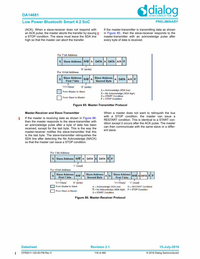
Datasheet Revision 2.1 15-July-2016
CFR0011-120-00-FM Rev 5 118 of 460 © 2016 Dialog Semiconductor
DA14681
Low Power Bluetooth Smart 4.2 SoC PRELIMINARY
(ACK). When a slave-receiver does not respond withan ACK pulse, the master aborts the transfer by issuinga STOP condition. The slave must leave the SDA linehigh so that the master can abort the transfer.
If the master-transmitter is transmitting data as shownin Figure 85:, then the slave-receiver responds to themaster-transmitter with an acknowledge pulse afterevery byte of data is received.
Master-Receiver and Slave-Transmitter
If the master is receiving data as shown in Figure 86:then the master responds to the slave-transmitter withan acknowledge pulse after a byte of data has beenreceived, except for the last byte. This is the way themaster-receiver notifies the slave-transmitter that thisis the last byte. The slave-transmitter relinquishes theSDA line after detecting the No Acknowledge (NACK)so that the master can issue a STOP condition.
When a master does not want to relinquish the buswith a STOP condition, the master can issue aRESTART condition. This is identical to a START con-dition except it occurs after the ACK pulse. The mastercan then communicate with the same slave or a differ-ent slave.
Figure 85: Master-Transmitter Protocol
Figure 86: Master-Receiver Protocol

Datasheet Revision 2.1 15-July-2016
CFR0011-120-00-FM Rev 5 119 of 460 © 2016 Dialog Semiconductor
DA14681
Low Power Bluetooth Smart 4.2 SoC PRELIMINARY
START BYTE Transfer Protocol
The START BYTE transfer protocol is set up for sys-tems that do not have an on-board dedicated I2C hard-ware module. When the I2C controller is addressed asa slave, it always samples the I2C bus at the highestspeed supported so that it never requires a STARTBYTE transfer. However, when I2C controller is a mas-ter, it supports the generation of START BYTE trans-fers at the beginning of every transfer in case a slave
device requires it. This protocol consists of seven zerosbeing transmitted followed by a 1, as illustrated in Fig-ure 87:. This allows the processor that is polling thebus to under-sample the address phase until 0 isdetected. Once the microcontroller detects a 0, itswitches from the under sampling rate to the correctrate of the master.
The START BYTE procedure is as follows:
1. Master generates a START condition.
2. Master transmits the START byte (0000 0001).
3. Master transmits the ACK clock pulse. (Presentonly to conform with the byte handling formatused on the bus)
4. No slave sets the ACK signal to 0.
5. Master generates a RESTART (R) condition.
A hardware receiver does not respond to the STARTBYTE because it is a reserved address and resets afterthe RESTART condition is generated.
25.4 MULTIPLE MASTER ARBITRATION
The I2C controller bus protocol allows multiple mastersto reside on the same bus. If there are two masters onthe same I2C-bus, there is an arbitration procedure ifboth try to take control of the bus at the same time bygenerating a START condition at the same time. Oncea master (for example, a microcontroller) has control ofthe bus, no other master can take control until the firstmaster sends a STOP condition and places the bus inan idle state.
Arbitration takes place on the SDA line, while the SCLline is 1. The master, which transmits a 1 while theother master transmits 0, loses arbitration and turns offits data output stage. The master that lost arbitrationcan continue to generate clocks until the end of thebyte transfer. If both masters are addressing the sameslave device, the arbitration could go into the dataphase. Figure 88: illustrates the timing of when twomasters are arbitrating on the bus.
For high-speed mode, the arbitration cannot go into thedata phase because each master is programmed witha unique high-speed master code. This 8-bitcode is
defined by the system designer and is set by writing tothe High Speed Master Mode Code Address Register,I2C_HS_MADDR. Because the codes are unique, onlyone master can win arbitration, which occurs by theend of the transmission of the high-speed master code.
Control of the bus is determined by address or mastercode and data sent by competing masters, so there isno central master nor any order of priority on the bus.
Arbitration is not allowed between the following condi-tions:
• A RESTART condition and a data bit
• A STOP condition and a data bit
• A RESTART condition and a STOP condition
Slaves are not involved in the arbitration process.
Figure 87: START BYTE Transfer

Datasheet Revision 2.1 15-July-2016
CFR0011-120-00-FM Rev 5 120 of 460 © 2016 Dialog Semiconductor
DA14681
Low Power Bluetooth Smart 4.2 SoC PRELIMINARY
25.5 CLOCK SYNCHRONIZATION
When two or more masters try to transfer informationon the bus at the same time, they must arbitrate andsynchronize the SCL clock. All masters generate theirown clock to transfer messages. Data is valid only dur-ing the high period of SCL clock. Clock synchronizationis performed using the wired-AND connection to theSCL signal. When the master transitions the SCL clockto 0, the master starts counting the low time of the SCLclock and transitions the SCL clock signal to 1 at thebeginning of the next clock period. However, if anothermaster is holding the SCL line to 0, then the master
goes into a HIGH wait state until the SCL clock linetransitions to 1.
All masters then count off their high time, and the mas-ter with the shortest high time transitions the SCL lineto 0. The masters then counts out their low time andthe one with the longest low time forces the other mas-ter into a HIGH wait state. Therefore, a synchronizedSCL clock is generated, which is illustrated in Figure89:. Optionally, slaves may hold the SCL line low toslow down the timing on the I2C bus.
Figure 88: Multiple Master Arbitration
Figure 89: Multiple Master Clock synchronization.

Datasheet Revision 2.1 15-July-2016
CFR0011-120-00-FM Rev 5 121 of 460 © 2016 Dialog Semiconductor
DA14681
Low Power Bluetooth Smart 4.2 SoC PRELIMINARY
25.6 OPERATION MODES
This section provides information on the following top-ics:
• Slave Mode Operation
• Master Mode Operation
• Disabling I2C controller
Note 8: It is important to note that the I2C controller should only be
set to operate as an I2C Master, or I2C Slave, but not both
simultaneously. This is achieved by ensuring that bit 6
(I2C_SLAVE_DISABLE) and 0 (I2C_MASTER_MODE) of
the I2C_CON register are never set to 0 and 1, respectively.
25.6.1 Slave Mode Operation
This section includes the following procedures:
• Initial Configuration
• Slave-Transmitter Operation for a Single Byte
• Slave-Receiver Operation for a Single Byte
• Slave-Transfer Operation For Bulk Transfers
Initial Configuration
To use the I2C controller as a slave, perform the follow-ing steps:
1. Disable the I2C controller by writing a ‘0’ to bit 0 ofthe I2C_ENABLE register.
2. Write to the I2C_SAR register (bits 9:0) to set theslave address. This is the address to which the I2Ccontroller responds.
3. Write to the I2C_CON register to specify which typeof addressing is supported (7- or 10-bit by setting bit 3).Enable the I2C controller in slave-only mode by writinga ‘0’ into bit 6 (I2C_SLAVE_DISABLE) and a ‘0’ to bit 0(MASTER_MODE).
Note 9: Slaves and masters do not have to be programmed with the
same type of addressing 7- or 10-bit address. For instance, a
slave can be programmed with 7-bit addressing and a mas-
ter with 10-bit addressing, and vice versa.
4. Enable the I2C controller by writing a ‘1’ in bit 0 ofthe I2C_ENABLE register.
Note 10: Depending on the reset values chosen, steps 2 and 3 may
not be necessary because the reset values can be config-
ured. For instance, if the device is only going to be a master,
there would be no need to set the slave address because
you can configure I2C controller to have the slave disabled
after reset and to enable the master after reset. The values
stored are static and do not need to be reprogrammed if the
I2C controller is disabled.
Slave-Transmitter Operation for a Single Byte
When another I2C master device on the bus addressesthe I2C controller and requests data, the I2C controlleracts as a slave-transmitter and the following stepsoccur:
1. The other I2C master device initiates an I2C transferwith an address that matches the slave address in theI2C_SAR register of the I2C controller.
2. The I2C controller acknowledges the sent addressand recognizes the direction of the transfer to indicatethat it is acting as a slave-transmitter.
3. The I2C controller asserts the RD_REQ interrupt (bit5 of the I2C_RAW_INTR_STAT register) and holds theSCL line low. It is in a wait state until softwareresponds. If the RD_REQ interrupt has been masked,due to I2C_INTR_MASK[5] register (M_RD_REQ bitfield) being set to 0, then it is recommended that ahardware and/or software timing routine be used toinstruct the CPU to perform periodic reads of theI2C_RAW_INTR_STAT register.
a. Reads that indicate I2C_RAW_INTR_STAT[5] (R_RD_REQ bit field) being set to 1 must be treated as the equivalent of the RD_REQ interrupt being asserted.
b. Software must then act to satisfy the I2C transfer.
c. The timing interval used should be in the order of 10 times the fastest SCL clock period the I2C con-troller can handle. For example, for 400 kb/s, the timing interval is 25us.
Note 11: The value of 10 is recommended here because this is
approximately the amount of time required for a single byte
of data transferred on the I2C bus.
4. If there is any data remaining in the TX FIFO beforereceiving the read request, then the I2C controllerasserts a TX_ABRT interrupt (bit 6 of theI2C_RAW_INTR_STAT register) to flush the old datafrom the TX FIFO.
Note 12: Because the I2C controller’s TX FIFO is forced into a
flushed/reset state whenever a TX_ABRT event occurs, it is
necessary for software to release the I2C controller from
this state by reading the I2C_CLR_TX_ABRT register before
attempting to write into the TX FIFO. See register
I2C_RAW_INTR_STAT for more details.
If the TX_ABRT interrupt has been masked, due to ofI2C_INTR_MASK[6] register (M_TX_ABRT bit field)being set to 0, then it is recommended that re-using thetiming routine (described in the previous step), or asimilar one, be used to read theI2C_RAW_INTR_STAT register.
a. Reads that indicate bit 6 (R_TX_ABRT) being set to 1 must be treated as the equivalent of the TX_ABRT interrupt being asserted.
b. There is no further action required from software.
c. The timing interval used should be similar to that described in the previous step for the I2C_RAW_INTR_STAT[5] register.
5. Software writes to the I2C_DATA_CMD register withthe data to be written (by writing a ‘0’ in bit 8).

Datasheet Revision 2.1 15-July-2016
CFR0011-120-00-FM Rev 5 122 of 460 © 2016 Dialog Semiconductor
DA14681
Low Power Bluetooth Smart 4.2 SoC PRELIMINARY
6. Software must clear the RD_REQ and TX_ABRTinterrupts (bits 5 and 6, respectively) of theI2C_RAW_INTR_STAT register before proceeding.
If the RD_REQ and/or TX_ABRT interrupts have beenmasked, then clearing of the I2C_RAW_INTR_STATregister will have already been performed when eitherthe R_RD_REQ or R_TX_ABRT bit has been read as1.
7. The I2C controller releases the SCL and transmitsthe byte.
8. The master may hold the I2C bus by issuing aRESTART condition or release the bus by issuing aSTOP condition.
Slave-Receiver Operation for a Single Byte
When another I2C master device on the bus addressesthe I2C controller and is sending data, the I2C control-ler acts as a slave-receiver and the following stepsoccur:
1. The other I2C master device initiates an I2C transferwith an address that matches the I2C controller’s slaveaddress in the I2C_SAR register.
2. The I2C controller acknowledges the sent addressand recognizes the direction of the transfer to indicatethat the I2C controller is acting as a slave-receiver.
3. I2C controller receives the transmitted byte andplaces it in the receive buffer.
Note 13: If the RX FIFO is completely filled with data when a byte is
pushed, then an overflow occurs and the I2C controller continues with subsequent I2C transfers. Because a NACK
is not generated, software must recognize the overflow when
indicated by the I2C controller (by the R_RX_OVER bit in
the I2C_INTR_STAT register) and take appropriate actions
to recover from lost data. Hence, there is a real time con-
straint on software to service the RX FIFO before the latter
overflow as there is no way to re-apply pressure to the
remote transmitting master. You must select a deep enough
RX FIFO depth to satisfy the interrupt service interval of their
system.
4. I2C controller asserts the RX_FULL interrupt(I2C_RAW_INTR_STAT[2] register).
If the RX_FULL interrupt has been masked, due to set-ting I2C_INTR_MASK[2] register to 0 or settingI2C_TX_TL to a value larger than 0, then it is recom-mended that a timing routine (described in “Slave-Transmitter Operation for a Single Byte”) be imple-mented for periodic reads of the “I2C_STATUS” onpage 138 register. Reads of the I2C_STATUS register,with bit 3 (RFNE) set at 1, must then be treated by soft-ware as the equivalent of the RX_FULL interrupt beingasserted.
5. Software may read the byte from theI2C_DATA_CMD register (bits 7:0).
6. The other master device may hold the I2C bus byissuing a RESTART condition or release the bus byissuing a STOP condition.
Slave-Transfer Operation For Bulk Transfers
In the standard I2C protocol, all transactions are singlebyte transactions and the programmer responds to aremote master read request by writing one byte into theslave’s TX FIFO. When a slave (slave-transmitter) isissued with a read request (RD_REQ) from the remotemaster (master-receiver), at a minimum there shouldbe at least one entry placed into the slave-transmitter’sTX FIFO.
I2C controller is designed to handle more data in theTX FIFO so that subsequent read requests can takethat data without raising an interrupt to get more data.Ultimately, this eliminates the possibility of significantlatencies being incurred between raising the interruptfor data each time had there been a restriction of hav-ing only one entry placed in the TX FIFO.
This mode only occurs when I2C controller is acting asa slave-transmitter. If the remote master acknowledgesthe data sent by the slave-transmitter and there is nodata in the slave’s TX FIFO, the I2C controller holdsthe I2C SCL line low while it raises the read requestinterrupt (RD_REQ) and waits for data to be writteninto the TX FIFO before it can be sent to the remotemaster.
If the RD_REQ interrupt is masked, due to bit 5(M_RD_REQ) of the I2C_INTR_STAT register beingset to 0, then it is recommended that a timing routinebe used to activate periodic reads of theI2C_RAW_INTR_STAT register. Reads ofI2C_RAW_INTR_STAT that return bit 5 (R_RD_REQ)set to 1 must be treated as the equivalent of theRD_REQ interrupt referred to in this section. This tim-ing routine is similar to that described in “Slave-Trans-mitter Operation for a Single Byte”
The RD_REQ interrupt is raised upon a read request,and like interrupts, must be cleared when exiting theinterrupt service handling routine (ISR). The ISR allowsyou to either write 1 byte or more than 1 byte into theTX FIFO. During the transmission of these bytes to themaster, if the master acknowledges the last byte. thenthe slave must raise the RD_REQ again because themaster is requesting for more data.
If the programmer knows in advance that the remotemaster is requesting a packet of n bytes, then whenanother master addresses I2C controller and requestsdata, the TX FIFO could be written with n number bytesand the remote master receives it as a continuousstream of data. For example, the I2C controller slavecontinues to send data to the remote master as long asthe remote master is acknowledging the data sent andthere is data available in the TX FIFO. There is noneed to hold the SCL line low or to issue RD_REQagain.
If the remote master is to receive n bytes from the I2Ccontroller but the programmer wrote a number of byteslarger than n to the TX FIFO, then when the slave fin-ishes sending the requested n bytes, it clears the TXFIFO and ignores any excess bytes.

Datasheet Revision 2.1 15-July-2016
CFR0011-120-00-FM Rev 5 123 of 460 © 2016 Dialog Semiconductor
DA14681
Low Power Bluetooth Smart 4.2 SoC PRELIMINARY
The the I2C controller generates a transmit abort(TX_ABRT) event to indicate the clearing of the TXFIFO in this example. At the time an ACK/NACK isexpected, if a NACK is received, then the remote mas-ter has all the data it wants. At this time, a flag is raisedwithin the slave’s state machine to clear the leftoverdata in the TX FIFO. This flag is transferred to the pro-cessor bus clock domain where the FIFO exists andthe contents of the TX FIFO is cleared at that time.
25.6.2 Master Mode Operation
This section includes the following topics:
• Initial Configuration
• Dynamic I2C_TAR or I2C_10BITADDR_MASTER Update
• Master Transmit and Master Receive
Initial Configuration
The procedures are very similar and are only differentwith regard to where the I2C_10BITADDR_MASTERbit is set (either bit 4 of I2C_CON register or bit 12 ofI2C_TAR register).
To use the I2C controller as a master perform the fol-lowing steps:
1. Disable the I2C controller by writing 0 to theI2C_ENABLE register.
2. Write to the I2C_CON register to set the maximumspeed mode supported (bits 2:1) and the desiredspeed of the I2C controller master-initiated transfers,either 7-bit or 10-bit addressing (bit 4).
Ensure that bit 6 I2C_SLAVE_DISABLE = 1 and bit 0MASTER_MODE =1
Note 14: Slaves and masters do not have to be programmed with the
same type of addressing 7- or 10-bit address. For instance, a
slave can be programmed with 7-bit addressing and a mas-
ter with 10-bit addressing, and vice versa.
3. Write to the I2C_TAR register the address of the I2Cdevice to be addressed (bits 9:0). This register alsoindicates whether a General Call or a START BYTEcommand is going to be performed by I2C.
4. Only applicable for high-speed mode transfers. Writeto the I2C_HS_MADDR register the desired mastercode for the I2C controller. The master code is pro-grammer-defined.
5. Enable the I2C controller by writing a 1 in bit 0 of theI2C_ENABLE register.
6. Now write transfer direction and data to be sent tothe I2C_DATA_CMD register. If the I2C_DATA_CMDregister is written before the I2C controller is enabled,the data and commands are lost as the buffers are keptcleared when I2C controller is disabled.
This step generates the START condition and theaddress byte on the I2C controller. Once I2C controlleris enabled and there is data in the TX FIFO, I2C con-troller starts reading the data.
Note 15: Depending on the reset values chosen, steps 2, 3, 4, and 5
may not be necessary because the reset values can be con-
figured. The values stored are static and do not need to be
reprogrammed if the I2C controller is disabled, with the
exception of the transfer direction and data.
25.6.3 Disabling I2C controller
The register I2C_ENABLE_STATUS is added to allowsoftware to unambiguously determine when the hard-ware has completely shutdown in response to theI2C_ENABLE register being set from 1 to 0. Only oneregister is required to be monitored.
Procedure:
1. Define a timer interval (ti2c_poll) equal to the 10times the signalling period for the highest I2C transferspeed used in the system and supported by I2C con-troller. For example, if the highest I2C transfer mode is400 kb/s, then this ti2c_poll is 25us.
2. Define a maximum time-out parameter,MAX_T_POLL_COUNT, such that if any repeated poll-ing operation exceeds this maximum value, an error isreported.
3. Execute a blocking thread/process/function that pre-vents any further I2C master transactions to be startedby software, but allows any pending transfers to becompleted.
Note 16: This step can be ignored if I2C controller is programmed to
operate as an I2C slave only.
4. The variable POLL_COUNT is initialized to zero.
5. Set I2C_ENABLE to 0.
6. Read the I2C_ENABLE_STATUS register and testthe I2C_EN bit (bit 0). Increment POLL_COUNT byone. If POLL_COUNT >= MAX_T_POLL_COUNT, exitwith the relevant error code.
7. If I2C_ENABLE_STATUS[0] is 1, then sleep forti2c_poll and proceed to the previous step.
Otherwise, exit with a relevant success code.

Datasheet Revision 2.1 15-July-2016
CFR0011-120-00-FM Rev 5 124 of 460 © 2016 Dialog Semiconductor
DA14681
Low Power Bluetooth Smart 4.2 SoC PRELIMINARY
26 InfraRed GeneratorThe InfraRed generator provides a flexible way oftransmitting any IR code used in remote controls. It hasan efficient message queue where users can describethe waveform of a specific IR command in just a fewbytes independently from the protocol. It sits on the 16-bit APB bus and receives a separate, up to 16MHzclock used for the carrier generation.
Features
• Carrier frequencies from 30 to 60 KHz
• Supports Pulse width and Pulse Distance encoding
• Supports Manchester encoding
• Supports Time mode (no carrier)
• Any combination of Mark and Space symbols
• Code FIFO of 32 16-bit words for encoding com-mands
• Automatic Repeat function, transparent to SW
• Interrupt generation upon transmit completion
26.1 ARCHITECTURE
The IR generator, is based upon the concept of usingtwo different ways of describing data, being able tosupport any IR protocol:
• Digital Message: This message represents a logic 1 or a logic 0 and is clearly described in form of Mark and Space duration as well as sequence.
• Paint Message: This message represents a totally custom "painted" waveform. The way of efficiently describing this, is to encode the symbol type (Mark/
Space) and the symbol duration within a code word for HW to be able to understand and proceed accordingly to the correct modulation.
The composition of a command consists of a numberof control words which contain information about digitalor paint messages in an efficient way. A breakdown ofthe well-known IR code NEC command is presented inthe following figure as an example:
Figure 90: InfraRed Generator Block Diagram
CARRIER GEN
INPUT STAGE OUTPUT STAGEMODULATOR
CarrierFrequencyGenerator30‐60KHz
PaintMessageGenerator
IR
APBInterface
Register File
DigitalMessageGenerator
APB
Code FIFO16bit x 32 depth
Repeat FIFO16bit x 8 depth
Message Decoding
From Register File
IRgen_clk
Figure 91: Paint/Digital messages on a NEC based example
Header
Paint Message
Address/Command
Digital Messages
Paint Message
Tail

Datasheet Revision 2.1 15-July-2016
CFR0011-120-00-FM Rev 5 125 of 460 © 2016 Dialog Semiconductor
DA14681
Low Power Bluetooth Smart 4.2 SoC PRELIMINARY
The encoding of the Paint/Digital messages can beimplemented according to the following tables:
So, basically, the MSbit of the word defines if the mes-sage is a digital or a paint one.
The block consists of four sub-blocks:
Input Stage
it consists of the APB interface the Register File, 2FIFOs and the Message Decoding engine. This sub-block is responsible for the configuration of the systemand the storage and decoding of the encoded words.These words will reside in the Code FIFO. The RepeatFIFO can be used to load special commands forrepeating a key press i.e. this is only protocol depend-ent. The output of the Code FIFO is decoded by theMessage Decoding engine and pushed in forms ofcommands into the next sub-block, the modulator. Thissub-block is also responsible for firing up the repeattimer in case that a key is constantly pressed. The rep-etition time as well the message to be sent variesaccording to the protocol.
Carrier Generator
This sub-block is responsible for the carrier frequencygeneration. It has its own gated clock which can be upto 16MHz and can generate frequencies in the range of30 - 60 KHz.
Modulator
This sub-block is responsible for the generation of themodulation signal which gates the carrier clock pulsetrain. The Modulator state machine select between dig-ital or pain message and controls the gate accordingly.
Output Stage
This sub-block can be programmed to invert the outputoptionally
26.2 PROGRAMMING
Initially the clock of the block has to be enabled byasserting the CLK_PER_REG[IR_CLK_ENABLE] bit.The carrier ON and OFF time in clock cycles have tobe programmed at IR_FREQ_CARRIER_Oxx_REGs.Following that, the logic one and zero are defined interms of clock cycles high (mark) and clock cycles low(zero) with help of the IR_LOGIC_ONE/ZERO_TIME_REGs
Another important feature that needs to be initialized iswhether the logic one/zero start with a mark and is fol-lowed by a zero, or the other way around. This isdefined in IR_CTRL_REG[IR_LOGIC_ONE_FORMAT]and IR_CTRL_REG[IR_LOGIC_ZERO_FORMAT]respectively. Finally, the time required for an automatedretransmit is defined at IR_REPEAT_TIME_REG.
Sending commands using a specific protocol is simplywriting the correct words into the Code FIFO and thenset IR_CTRL_REG[IR_TX_START] to trigger the trans-mission. The actual word values have to comply to theencoding schemes as presented in Table 50 and Table51.
Table 50: IR Digital Message Encoding
Bit Name Description
15 Message Type
1 = Digital message. That means that the message information itself defines logic 1 or logic 0
14:11 Message Length
Number of valid bits minus 1. Range 0 to 10
10:0 Message Payload
Digital Message consist-ing of logic 1s and logic 0s
Table 51: IR Paint Message Encoding
Bit Name Description
15 Message Type
0 = Paint message
14 Symbol Type
1 = Mark 0 = Space
13:0 Duration Mark/Space duration in carrier clock cycles

Datasheet Revision 2.1 15-July-2016
CFR0011-120-00-FM Rev 5 126 of 460 © 2016 Dialog Semiconductor
DA14681
Low Power Bluetooth Smart 4.2 SoC PRELIMINARY
27 Quadrature DecoderThe DA14681 has a integrated quadrature decoderthat can automatically decode the signals for the X, Yand Z axes of a HID input device, reporting step countand direction. This block can be used for waking up thechip as soon as there is any kind of movement from theexternal device connected to it. The block diagram ofthe quadrature decoder is presented in Figure 92.
Features
• Three 16-bit signed counters that provide the step count and direction on each of the axes (X, Y and Z)
• Programmable system clock sampling at maximum 16 MHz.
• APB interface for control and programming
• Programmable source from P0, P1 and P2 ports
• Digital filter on the channel inputs to avoid spikes
27.1 ARCHITECTURE
Channels are expected to provide a pulse train with 90degrees rotation as displayed in Figure 93 and Figure94.
Depending on whether channel A or channel B is lead-ing in phase, the quadrature decoding block calculatesthe direction on the related axis. Furthermore, thesigned counter value represents the number of stepsmoved.
27.2 PROGRAMMING
Since six channels are required (two for each axis),any GPIO can be mapped onto this block. The usercan choose which GPIOs to use for the channels byprogramming the Pxy_MODE_REG[PID] with valuesfrom 30 up to 44.
The digital filter eliminates any spike shorter than twoclock periods. The counter holds the movement eventsof the channel. When a channel is disabled the counteris reset. The counters are accessible via the APB bus.
The quadrature decoder operates on the system clock.The QDEC_CLOCKDIV register defines the number ofclock cycles of the period at which the decoding logicsamples the data on the channel inputs.
The interrupt block monitors the movement events andgenerates an interrupt every N events. The value for Nis defined in the QDEC_CTRL register.
Note: if there are events from multiple channels in thesame cycle, the interrupt event counter is onlyincreased by one.
Figure 92: Block diagram of the Quadrature Decoder
Register File
16-bit Counter (X Axis)
Digita
l F
ilter
ChX_A
ChX_B
16-bit Counter (Y Axis)
Digita
l F
ilter
ChY_A
ChY_B
16-bit Counter (Z Axis)
Digita
l F
ilter
ChZ_A
ChZ_B
Interrupt Generator
APB Interface
Quad_Dec_IRQ
Figure 93: Moving forward on axis X
Figure 94: Moving backwards on axis X
ChX_A
ChX_B
ChX_A
ChX_B
ChX_A
ChX_B
ChX_A
ChX_B

Datasheet Revision 2.1 15-July-2016
CFR0011-120-00-FM Rev 5 127 of 460 © 2016 Dialog Semiconductor
DA14681
Low Power Bluetooth Smart 4.2 SoC PRELIMINARY
28 Keyboard ScannerThe Keyboard Scanner is a programmable hardwarestate machine which takes care of scanning the key-board matrix and providing a clear view of key presses/releases to SW. Once enabled, it takes care of any keypress or release without interfering with the CPU up tothe point that a de-bounced key press is identified. Itoperates at a programmable frequency clock, allowingfor a very short scan cycle time. Debouncing of up to12 simultaneous keys is allowed with dedicated coun-ters. The resulting events are reported in a FIFO whichtriggers an interrupt to the CPU at the end of the scancycle.
The block diagram of the Keyboard Controller is pre-sented in Figure 95.
Features
• Autonomous keyboard matrix scan without CPU interference
• 250 kHz clock for low power
• Maximum 16 Rows / 32 Columns support for any GPIO
• Up to 12, 7-bit de-bounce counters, counting matrix scan cycles
• Different press and release debounce times support
• Configurable row activation time
• Short scan cycle (1.3 us for a 10x10 matrix using 16 MHz clock)
• Row/Column report for a key press/release
28.1 ARCHITECTURE
The Keyboard Scanner comprises a Key Monitoringstate machine which controls the 12 Debouncing Mod-ules, a Matrix Scan state machine which is responsiblefor a totally automated scan of the preferred key matrix,a FIFO which reports to the CPU what has beenpressed/released and an APB based register file whichis used to configure the block. A Scrambler is also uti-lized to allow for flexibility in selecting GPIOs used asrows or columns in the key matrix. Finally, the KeyMonitor gathers the column/row identities for an event(key press or release), controls the 12 debouncingmodules and writes the message into the FIFO trigger-ing an interrupt to the CPU.
The Scrambler is implementing the assignment of spe-cific GPIOs as rows (outputs) or columns (inputs) toform a matrix as shown in the example of Figure 96.
Figure 95: Keyboard Scanner block diagram
Keyboard Scanner
APB interface
Registerfile
Fifomessage
MatrixScan
Debounce Module #1
Debounce Module #2
Debounce Module #12
Key monitor
Rows
Columns
Valid
Row
Column
Message
WE
Full
Scrambler
. . .
To/from GPIOs
APB16
Figure 96: 4x4 Keyboard Matrix example
Columns (y)
Rows(x)
x0
x1
x2
x3
y0 y1 y2 y3

Datasheet Revision 2.1 15-July-2016
CFR0011-120-00-FM Rev 5 128 of 460 © 2016 Dialog Semiconductor
DA14681
Low Power Bluetooth Smart 4.2 SoC PRELIMINARY
The configuration of the GPIOs can be realized withuse of the KBSCN_GPIOx_MODE_REG. The actualsize of the matrix shouild be programmed inKBSCN_MATRIX_SIZE_REG.
The Matrix Scan block implements a finite state
machine which takes care of the full scanning of thekey matrix without the CPU intervention. The scancycle is presented in the following figure:
The FSM is setting each row to ‘0’, waits for a pre-con-figured amount of time (activation time, programmed inKBSCN_CTRL2_REG) and then it reads the columnsvector. If no zeros are sensed in the columns word, itcontinues scanning until all rows have been exercised.If there is a press while scanning, a flag (KEY_STAT)changes value. As soon as the whole matrix has beenscanned, the debouncer modules are started. Theseare incremented per scan cycle until a programmedvalue is reached (KBSCN_DEBOUNCE_REG). Up to12 concurrent debouncing operations are supported.
Following that, the FSM checks on the inactivity of thekey matrix. KBSCN_CTRL_REG[KBSCN_INACTIVE_EN]=1 will automatically stop the
scanning activity ifKBSCN_CTRL_REG[KBSCN_INACTIVE_TIME] scancycles have elapsed without any key press. If not set,then the scanning activity will keep on.
A key press/release message is prepared and stored inthe FIFO for the CPU after every scan cycle providedthat an even has been sensed. Each message is 11 bitwide and can be read atKBSCN_MESSAGE_KEY_REG. Multiple messagesare possible in the case of multiple events (presses orreleases). Its structure is presented in the table below:
Figure 97: Scan cycle state machine
Scan Cycle Start
Have all Rows been traversed?
NO
NO
YESCHECKDEBOUNCE
Set CUR_ROW= firstSet KEY_STAT = Not
Pressed
Drive CUR_ROW to low
Wait for Row Activation Time
Read Columns
Set KEY_STAT = Pressed
Are Columns all = 0?
YES
Set CUR_ROW=NEXT_ROW
NO
Is Inactive counter reached and enable
set?
YES
Scan Cycle End
Is KEY_STAT= Pressed?
YesNo
Reset Inactive counter
Increase Inactive counter

Datasheet Revision 2.1 15-July-2016
CFR0011-120-00-FM Rev 5 129 of 460 © 2016 Dialog Semiconductor
DA14681
Low Power Bluetooth Smart 4.2 SoC PRELIMINARY
An interrupt is triggered towards the CPU in threecases:
1. A message has been placed in the messageFIFO
2. There is an underflow/overflow of the messageFIFO
3. The inactive time (in scan cycles) has elapsed
This information as well as the actual amount of mes-sages residing in the FIFO can be accessed atKBSCN_STATUS_REG. Note that, the FIFO can beerased by SW usingKBSCN_CTRL_REG[KBSCN_RESET_FIFO].
The number of KEYB_CLK cycles required for a fullscan cycle is given by the formula below:
Cscan= NROWS* (CACT+2), where CACT is the amount ofclocks for the activation time as programmed inKBSCN_CTRL2_REG and NROWS the number of rows.
The clock can be 250 kHz up to 96 MHz if the PLL isenabled.
28.2 PROGRAMMING
To initialize the Keyboard Scanner, the clock has to befirst enabled by settingCLK_PER_REG[KBSCAN_ENABLE]=1 andKBSCN_CTRL_REG[KBSCN_CLKDIV] to the pre-ferred value. The latter defines the clock frequency ofthe block.
Following that, the columns have to be programmed inoutput mode via the Pxy_MODE_REG registers. Thereis a dedicated PID for this namely number 47(KB_ROW). The columns have to be explicitly definedas pulled-up inputs with use of the respectivePxy_MODE_REG registers.
Both rows and columns need to be defined in theKBSCN_GPIOz_MODE_REG so that the KeyboardScanner understands which I/O is what.
The row active time, i.e. the time needed for the keymatrix to settle after applying a high or low has to beprogrammed in KBSCN_ROW_ACTIVE_TIME. This
value represents keyboard scanner clock cycles.
The Matrix size has to be configured inKBSCN_MATRIX_SIZE_REG and the debounce timesfor press and release (can be different) should be pro-grammed at KBSCN_DEBOUNCE_REG. Reset valueis 0x1 which means no debounce at all.
A special feature enables the scanning to automaticallystop afterKBSCN_CTRL_REG[KBSCN_INACTIVE_TIME] clockcycles have elapsed without activity. Last thing to do forthe initialization is enable the interrupt of the KeyboardScanner byKBSCN_CTRL_REG[KBSCN_IRQ_FIFO_MASK] = 1andKBSCN_CTRL_REG[KBSCN_IRQ_MESSAGE_MASK] = 1 and enable the block by settingKBSCN_CTRL_REG[KBSCN_EN]=1.
The interrupt triggers the CPU to read a messageresiding in the 12-words FIFO by reading theKBSCN_MESSAGE_KEY_REG. This message con-tains the key id that was recently pressed or releasedas well as the indication of being or not, the only mes-sage in the FIFO (KBSCN_LAST_ENTRY).
Table 52: Keyboard Scanner Message Structure
Bit Description
10 Designates if this is the last message of this scan cycle. If it is high, then the value if the register is 0xFF (the rest of the bits are all high as well)
9 Key state. 0: key is pressed, 1: key is released
8:4 Defines the number of the column of the key event
3:0 Defines the number of the row of the key event

Datasheet Revision 2.1 15-July-2016
CFR0011-120-00-FM Rev 5 130 of 460 © 2016 Dialog Semiconductor
DA14681
Low Power Bluetooth Smart 4.2 SoC PRELIMINARY
29 Software TimersThe Software Timer block contains 3 timer modulesthat are software controlled, programmable and can beused for various tasks. Timer0 is a 16-bit general pur-pose timer with a PWM output capability. Timer2 is a14-bit counter that generates three identical PWM sig-nals in a quite flexible manner.
29.1 TIMER0
Timer0 is a 16-bit general purpose software program-mable timer, which has the ability of generating PulseWidth Modulated signals, namely PWM0 and PWM1. Italso generates the SWTIM_IRQ interrupt to the ARMCortex M0. It can be configured in various modesregarding output frequency, duty cycle and the modula-tion of the PWM signals.
Features
• 16-bit general purpose timer
• Ability to generate 2 Pulse Width Modulated signals (i.e. PWM0 and PWM1)
• Programmable output frequency: f = (16, 8, 4, 2 MHz or 32 kHz) / (M+1)+(N+1)with N = 0 to (2**16)-1, M = 0 to (2**16)-1
• Programmable duty cycle: = (M+1)/((M+1)+(N+1)) *100%
• Separately programmable interrupt timer:T = (16, 8, 4, 2 MHz or 32 kHz) / (ON+1)
Figure 98 shows the block diagram of Timer0. The 16bits timer consists of two counters: T0-counter and ON-counter, and three registers:TIMER0_RELOAD_M_REG,TIMER0_RELOAD_N_REG and TIMER0_ON_REG.Upon reset, the counter and register values are0x0000. Timer0 will generate a Pulse Width Modulatedsignal PWM0. The frequency and duty cycle of PWM0are determined by the contents of theTIMER0_RELOAD_N_REG and theTIMER0_RELOAD_M_REG registers.
The timer can run at five different clocks: 16 MHz, 8MHz, 4 MHz, 2 MHz or 32 kHz. The 32 kHz clock isselected by default with bit TIM0_CLK_SEL in theTIMER0_CTRL_REG register. This ‘slow’ clock has no
enabling bit. The other four options can be selected bysetting the TIM0_CLK_SEL bit and the TMR_ENABLEbit in the CLK_PER_REG (default disabled). This reg-ister also controls the frequency via the TMR_DIV bits.An extra clock divider is available that can be activatedvia bit TIM0_CLK_DIV of the timer control registerTIMER0_CTRL_REG. This clock divider is only usedfor the ON-counter and always divides by 10.
Timer0 operates in PWM mode. The signals PWM0and PWM1 can be mapped to any GPIOs.
Timer0 PWM mode
If bit TIM0_CTRL in the TIMER0_CTRL_REG is set,Timer0 will start running. SWTIM_IRQ will be gener-ated and the T0-counter will load its start value from
Figure 98: Timer0 block diagram
LSBreg Timer0
MSBreg
TIMER0_RELOAD_N_REG
LSBreg MSBreg
Compare
LSBreg MSBreg
If T0-counter = 0 then T0_toggle = ~T0_toggle
T0_ge_M0TIM0_INT
ON-counter
LSBshadow MSBshadow LSBshadow MSBshadow
loadnewloadnew0 01 1
-1
0 1
T0-counter=0 1 0
1 0loadnew
loadnew
loadnew
LSBreg MSBreg
TIMER0_0N_REG
LSBreg MSBreg
T0-counter
TIMER0_RELOAD_M_REG
T0-toggle
Interrupt generation:PWM mode:
if (T0_toggle=0 andON-counter=0) ORTIM0_CTRL =0->1
December 13, 2012
PWM0
PWM1
to GPIOIf PWM_MODE = 1 then AND signal with clock
If PWM_MODE = 1 then AND signal with clock
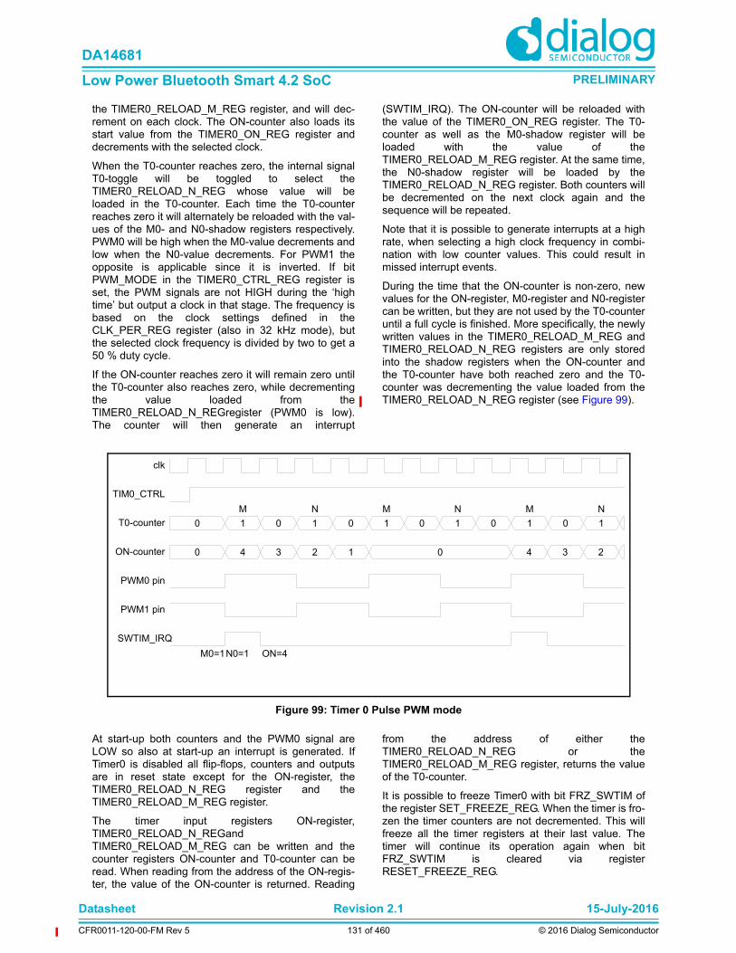
Datasheet Revision 2.1 15-July-2016
CFR0011-120-00-FM Rev 5 131 of 460 © 2016 Dialog Semiconductor
DA14681
Low Power Bluetooth Smart 4.2 SoC PRELIMINARY
the TIMER0_RELOAD_M_REG register, and will dec-rement on each clock. The ON-counter also loads itsstart value from the TIMER0_ON_REG register anddecrements with the selected clock.
When the T0-counter reaches zero, the internal signalT0-toggle will be toggled to select theTIMER0_RELOAD_N_REG whose value will beloaded in the T0-counter. Each time the T0-counterreaches zero it will alternately be reloaded with the val-ues of the M0- and N0-shadow registers respectively.PWM0 will be high when the M0-value decrements andlow when the N0-value decrements. For PWM1 theopposite is applicable since it is inverted. If bitPWM_MODE in the TIMER0_CTRL_REG register isset, the PWM signals are not HIGH during the ‘hightime’ but output a clock in that stage. The frequency isbased on the clock settings defined in theCLK_PER_REG register (also in 32 kHz mode), butthe selected clock frequency is divided by two to get a50 % duty cycle.
If the ON-counter reaches zero it will remain zero untilthe T0-counter also reaches zero, while decrementingthe value loaded from theTIMER0_RELOAD_N_REGregister (PWM0 is low).The counter will then generate an interrupt
(SWTIM_IRQ). The ON-counter will be reloaded withthe value of the TIMER0_ON_REG register. The T0-counter as well as the M0-shadow register will beloaded with the value of theTIMER0_RELOAD_M_REG register. At the same time,the N0-shadow register will be loaded by theTIMER0_RELOAD_N_REG register. Both counters willbe decremented on the next clock again and thesequence will be repeated.
Note that it is possible to generate interrupts at a highrate, when selecting a high clock frequency in combi-nation with low counter values. This could result inmissed interrupt events.
During the time that the ON-counter is non-zero, newvalues for the ON-register, M0-register and N0-registercan be written, but they are not used by the T0-counteruntil a full cycle is finished. More specifically, the newlywritten values in the TIMER0_RELOAD_M_REG andTIMER0_RELOAD_N_REG registers are only storedinto the shadow registers when the ON-counter andthe T0-counter have both reached zero and the T0-counter was decrementing the value loaded from theTIMER0_RELOAD_N_REG register (see Figure 99).
At start-up both counters and the PWM0 signal areLOW so also at start-up an interrupt is generated. IfTimer0 is disabled all flip-flops, counters and outputsare in reset state except for the ON-register, theTIMER0_RELOAD_N_REG register and theTIMER0_RELOAD_M_REG register.
The timer input registers ON-register,TIMER0_RELOAD_N_REGandTIMER0_RELOAD_M_REG can be written and thecounter registers ON-counter and T0-counter can beread. When reading from the address of the ON-regis-ter, the value of the ON-counter is returned. Reading
from the address of either theTIMER0_RELOAD_N_REG or theTIMER0_RELOAD_M_REG register, returns the valueof the T0-counter.
It is possible to freeze Timer0 with bit FRZ_SWTIM ofthe register SET_FREEZE_REG. When the timer is fro-zen the timer counters are not decremented. This willfreeze all the timer registers at their last value. Thetimer will continue its operation again when bitFRZ_SWTIM is cleared via registerRESET_FREEZE_REG.
Figure 99: Timer 0 Pulse PWM mode
0 1 0 1 0 1 0 1 0 1 0 1
0 4 3 2 1 0 4 3 2
M NNMNM
M0=1N0=1 ON=4
clk
TIM0_CTRL
T0-counter
ON-counter
PWM0 pin
PWM1 pin
SWTIM_IRQ

Datasheet Revision 2.1 15-July-2016
CFR0011-120-00-FM Rev 5 132 of 460 © 2016 Dialog Semiconductor
DA14681
Low Power Bluetooth Smart 4.2 SoC PRELIMINARY
29.2 TIMER1
Timer1 is a 16-bit up/down timer with capture input (2channels) and one shot pulse capability. This timer isalso able of generating a PWM signal with programma-ble output frequency. Timer1 is the only timer that staysalive when the DA14681 is in sleep mode. It countsusing the sleep clock and can still control one output,namely the P0_6 while the rest of the IOs are frozen toreduce power dissipation.
Features
• 16-bit general purpose timer
• Generates a Pulse Width Modulated signal (PWM5)
• 2 channels for capture input triggering
• One shot pulse with programmable pulse width
• 16-bit clock pre-scaler
• Up/down counting capability with free running mode
• Operating at sleep clock when system is in sleep mode
• Counts while in Extended Sleep mode.
• PW5 controls the P0_6 output while in Extended Sleep mode
• Programmable output frequencyF = 16 MHz/2 to 16 MHz/((2**14)-1)
• Dedicated interrupt line
Timer1 is enabled byCAPTIM_CTRL_REG[CAPTIM_EN] bit. This is theonly timer that supports up/down counting with meansof programming the CAPTIM_CTRL_REG[CAPTIM_COUNT_DOWN_EN] bit.
Timer1 supports capturing 2 externally triggered events(positive or negative edges) on GPIOs that can beselected. When the first event is captured, the currentvalue of the 16-bit free-running timer is stored into
CAPTIM_CAPTURE_GPIO1_REG while upon trigger-ing of the second event, the current timer value isstored into CAPTIM_CAPTURE_GPIO2_REG. In thisway, the timing interval between 2 successive eventscan be measured with precision.
The Timer1 support one shot pulse(CAPTIM_CTRL_REG[CAPTIM_ONESHOT_MODE_EN]). Whenever either of the two externally selectedGPIOs triggers an event, a programmable width pulse
Figure 100: PWM Timer 1 block diagram
TRIPLE_PWM_FREQ
T1_CNTR
PWM5_DUTY
16 bits
13 013 0
Reset
SetSys clk
System bus
+1
TIMER1
T1_PWM5
PWM5_FREQ
13 0
Comparatorsequal
resetHold
CaptureEvent
Capture Word 1
Capture Word 2
One Pulsehot
16-bit Prescalerslp_clk
GPIOs
GPIOs

Datasheet Revision 2.1 15-July-2016
CFR0011-120-00-FM Rev 5 133 of 460 © 2016 Dialog Semiconductor
DA14681
Low Power Bluetooth Smart 4.2 SoC PRELIMINARY
(CAPTIM_SHOTWIDTH_REG) will be output onanother GPIO programmed byPxx_MODE_REG[PID]=53. Furthermore, the time upto the start of the pulse is again configurable byCAPTIM_RELOAD_REG.
Timer1 is kept alive while the system is in ExtendedSleep mode. The PWM5 signal which can be config-ured by CAPTIM_PWM_FREQ_REG andCAPTIM_PWM_DC_REG with respect to the fre-quency and duty cycle is automatically connected tothe P0_6 pin output buffer. Hence, if enabled
(CLK_TMR_REG[P06_TMR1_PWM_MODE]=1), P0_6can be driving external devices even during extendedsleep.
Note that, the PWM functionality is decoupled from thetimer1 counting which can be read atCAPTIM_TIMER_VAL_REG at any given time whilethe chip is in active mode.
An overview of the timer modes, reset values and inter-rupt generation is presented in the following table:
29.3 TIMER2
Timer2 has three Pulse Width Modulated (PWM) out-puts. The block diagram in shown in Figure 101:.
Features
• 14-bit general purpose timer
• Generates 3 Pulse Width Modulated signals (i.e. PWM2, PWM3 and PWM4)
• Input Clock frequency 16 MHz
• Programmable output frequencyF = 16 MHz/2 to 16 MHz/((2**14)-1)
• Three outputs with Programmable duty cycle from 0% to 100%
• Used for white LED intensity (on/off) control
Table 53: Timer1 interrupt generation
Mode Reset Value Interrupt Generated
Count up with Reload 0 When reload value reached
Count down with Reload CAPTIM_RELOAD_REG When 0 reached
Count up free running 0 When reload value reached

Datasheet Revision 2.1 15-July-2016
CFR0011-120-00-FM Rev 5 134 of 460 © 2016 Dialog Semiconductor
DA14681
Low Power Bluetooth Smart 4.2 SoC PRELIMINARY
The Timer2 is clocked with the system clock (16 MHz)and can be enabled withTRIPLE_PWM_CTRL_REG[TRIPLE_PWM_ENABLE].
T2_FREQ_CNTR determines the output frequency ofthe T2_PMWn output. This counter counts down fromthe value stored in registerTRIPLE_PWM_FREQUENCY. At counter value 0,T2_FREQ_CNTR sets the T2_PWMn output to ‘1’ andthe counter is reloaded again.
T2_DUTY_CNTR is an up-counter that determines theduty cycle of the T2_PWMn output signal. After theblock is enabled, the counter starts from 0. IfT2_DUTY_CNTR is equal to the value stored in therespective PWMn_DUTY_CYCLE register, this resetsthe T2_PWMn output to 0. T2_DUTY_CNTR is resetwhen TRIPLE_PWM_FREQUENCY is 0.
Note that the value of PWMn_DUTY_CYCLE must beless or equal than TRIPLE_PWM_FREQUENCY.
Another feature of Timer2 PWM signals is the fact thatthe start and end cycle of the PWM wave can be pro-grammed separately for the three signals using thePWMx_START_CYCLE and PWMx_END_CYCLE. Inthis way, the PWM signals can be configured to imple-
ment a certain phase shift. These signals also controlthe LED pins with means ofLED_CONTROL_REG[LEDx_SRC_SEL].
The Timer2 is enabled/disabled by programming theTRIPLE_PWM_CTRL_REG[TRIPLE_PWM_EN] bit.
The timing diagram of Timer2 is shown in Figure 102.
Freeze function
During RF activity it may be desirable to temporarilysuppress the PWM switching noise. This can be doneby settingTRIPLE_PWM_CTRL_REG[HW_PAUSE_EN] = 1.The effect is that whenever there is a transmission or areception process from the Radio, T2_DUTY_CNTR isfrozen and T2_PWMx output is switched to ‘0’ to disa-ble the selected T2_PWM1, T2_PWM2, T2_PWM3. Assoon as the Radio is idle (i.e. RX_EN or TX_EN signalsare zero), T2_DUTY_CNTR resumes counting andfinalizes the remaining part of the PWM duty cycle.
TRIPLE_PWM_CTRL_REG[SW_PAUSE_EN] can beset to ‘0’ to disable the automatic, hardware drivenfreeze function of the duty counter and keep the dutycycle constant.
Figure 101: PWM Timer 2 block diagram
TRIPLE_PWM_FREQ
T2_DUTY_CNTR
3x14 bits
PWM2_DUTY
14 bits
13 013 0
Reset
Set
equal1
=0
16 MHz
System bus
+1
+1
TRIPLE_PWM_ENABLE
/Reset block
Set
Reset
TIMER2
T2_PWM1
T2_PWM2
PWM3_DUTY
13 0
Comparatorsequal2
-1
reset
14 bits
Hold
T2_FREQ_CNTR
TRIPLE_PWM_CTRL_REG
RX_EN
PWM4_DUTY
13 0
Set
Reset
equal3
T2_PWM3
TX_EN
SW_PAUSE_EN
HW_PAUSE_EN
TRIPLE_PWM_CTRL_REG

Datasheet Revision 2.1 15-July-2016
CFR0011-120-00-FM Rev 5 135 of 460 © 2016 Dialog Semiconductor
DA14681
Low Power Bluetooth Smart 4.2 SoC PRELIMINARY
Note that the RX_EN and TX_EN signals are not soft-ware driven but controlled by the BLE core hardware.
29.4 BRTH_TIMER
This timer implements an automated breathing functionfor external LEDs without software interference. Theresulting PWM signal can be mapped on any of theGPIOs of the system. It uses the system clock as input.
Features
• Maximum and minimum duty cycle configuration
• PWM duty cycle step granularity up to 256
• Input clock frequency 16 MHz
• Programmable output frequencyf = fsystem /(1 to 256) MHz
Figure 102: Timer 2 PWM timing diagram
0 0 1 2 2 2 3 .. ... 0 1 2 3
N N N-1 N-2 N-3 ... ... 1 0 N N-1 N-2 N-3
CLK (16 MHz)
TRIPLE_PWN_EN
T2_DUTY_CNTR
T2_FREQ_CNTR
T2_PWMn

Datasheet Revision 2.1 15-July-2016
CFR0011-120-00-FM Rev 5 136 of 460 © 2016 Dialog Semiconductor
DA14681
Low Power Bluetooth Smart 4.2 SoC PRELIMINARY
30 Watchdog TimerThe watchdog timer is an 8-bit timer with sign bit thatcan be used to detect an unexpected executionsequence caused by a software run-away and cangenerate a full system reset or a Non-Maskable Inter-rupt (NMI). Upon expiration, a HW reset is triggered.
Features
• 8 bits down counter with sign bit, clocked with a 10.24 ms clock for a maximum 2.6 s time-out.
• Non-Maskable Interrupt (NMI) or WDOG reset.
• Optional automatic WDOG reset if NMI handler fails to update the Watchdog register.
• Non maskable Watchdog freeze of the Cortex-M0 Debug module when the Cortex-M0 is halted in Debug state.
• Maskable Watchdog freeze by user program.
The 8 bits watchdog timer is decremented by 1 every10.24 ms. The timer value can be accessed throughthe WATCHDOG_REG register which is set to 255(FF16) at reset. This results in a maximum watchdogtime-out of ~2.6 s. During write access theWATCHDOG_REG[WDOG_WEN] bits must be 0. Thisprovides extra filtering for a software run-away writingall ones to the WATCHDOG_REG. If the watchdogcounter reaches 0, the counter value will get a negativevalue by setting bit 8. The counter sequence becomes1, 0, 1FF16 (-1), 1FE16(-2),...1F016 (-16).
If WATCHDOG_CTRL_REG[NMI_RST] = 0, the watch-dog timer will generate an NMI if the watchdog timerreaches 0 and a WDOG reset if the counter becomesless or equal to -16 (1F016). The NMI handler mustwrite any value > -16 to the WATCHDOG_REG to pre-vent the generation of a WDOG reset at counter value -16 after 16*10.24 = 163.8 ms.
If WATCHDOG_CTRL_REG[NMI_RST] = 1, the watch-dog timer generates a WDOG reset if the timerbecomes less or equal than 0.
The WDOG reset is one of the SYS (system) resetsources and resets the whole device, including settingthe WATCHDOG_REG register to 255, except for theRST pin, the Power On reset, the HW reset and theDBG (debug module) reset. Since the HW reset is not
triggered, the SYS_CTRL_REG[REMAP_ADR0] bitswill retain their value and the Cortex-M0 will start exe-cuting again from the current selected memory ataddress zero. Refer to the “Reset” chapter for an over-view of the complete reset circuit and conditions.
For debugging purposes, the Cortex-M0 Debug mod-ule can always freeze the watchdog by setting theDHCSR[DBGKEY | C_HALT | C_DEBUGEN] controlbits (reflected by the status bit S_HALT). This is auto-matically done by the debug tool, e.g. during step-by-step debugging. Note that this bit also freezes theWakeup Timer, the Software Timer and the BLE masterclock. For additional information also see theDEBUG_REG[DEBUGS_FREEZE_EN] mask register.The C_DEBUGEN bit is not accessible by the usersoftware to prevent freezing the watchdog.
In addition to the S_HALT bit, the watchdog timer canalso be frozen if NMI_RST=0 and SET_FREEZE_REG[FRZ_WDOG] is set to ‘1’. The watchdog timerresumes counting whenRESET_FREEZE_REG[FRZ_WDOG] is set to ‘1’. TheWATCHDOG_CTRL_REG[NMI_RST] bit can only beset by software and will only be reset on a SYS reset.
Figure 103: Watchdog Timer block diagram
NMI
SetReset
Set by Software
0
1
WATCHDOG_REG[8-0]
Watchdog timer10.24 ms
WDOG reset<= 0
WATCHDOG_CTRL_REG[NMI_RST]
<= -16
Reset to 0 Reset to 0xFF Set
Reset
(default)
Freeze
DHCSR[S_HALT]
Cortex-M0 (debug) by SYS reset
SET_FREEZE_REG
[FRZ_WDOG]
RESET_FREEZE_REG
[FRZ_WDOG]
by SYS reset
Set
Reset
0
1
NMI_RST
OR
Freeze Wakeup Timer, Software Timer, BLE master clock
= 00
1
Bits[15-9] =0
Write_enable

Datasheet Revision 2.1 15-July-2016
CFR0011-120-00-FM Rev 5 137 of 460 © 2016 Dialog Semiconductor
DA14681
Low Power Bluetooth Smart 4.2 SoC PRELIMINARY
31 USB InterfaceThe USB interface is an integrated USB Node control-ler compatible with the full and low speed USB specifi-cation version 1.1.
It integrates a Serial Interface Engine (SIE) and USBendpoint (EP) FIFOs. Seven endpoint pipes are sup-ported: one for the mandatory control endpoint and sixto support interrupt endpoints. Each endpoint pipe hasa dedicated FIFO, 8 bytes for the control endpoint and64 bytes for the other endpoints.
The USB transceiver module is accessed throughUSB_Dp and USB_Dm pins.
Features
• Full Speed USB node
• Interfaces to USB V1.1 transceiver with programma-ble rise and fall times and integrated D+/D- pull-up resistors.
• Serial Interface Engine (SIE) consisting of a Media Access Controller (MAC), USB Specification 1.0 and 1.1 compliant
• USB Function Controller with seven FIFO-based Endpoints:
• One bidirectional Control Endpoint 0 (8 bytes)
• Three Transmit Endpoints (64 bytes each)
• Three Receive Endpoints (64 bytes each)
• Automatic Data PID toggling/checking and NAK packet recovery (maximum 256 x32 bytes of data = 8 kB)
Figure 104: USB Node block diagram
Endpoint/Control FIFOs
SIE
System bus
USB TransceiverModule
Control Status
End
poin
t0 EP
1E
P1
EP
3E
P3
RX
TX
Media Access Controller (MAC)ClockRecovery
Physical Layer Interface (PHY) USB EventDetect
VDD_USBVSS USB_Dp USB_Dm
6/48MHz Clock
USBFS_IRQ
(OUT)
(IN)
LDO_USB
VBUS
500 kOhm
500 kOhm

Datasheet Revision 2.1 15-July-2016
CFR0011-120-00-FM Rev 5 138 of 460 © 2016 Dialog Semiconductor
DA14681
Low Power Bluetooth Smart 4.2 SoC PRELIMINARY
31.1 SERIAL INTERFACE ENGINE
The SIE is comprised of physical (PHY) and MediaAccess Controller (MAC) modules. The PHY moduleincludes the digital-clock recovery circuit, a digital glitchfilter, End Of Packet (EOP) detection circuitry, and bitstuffing and unstuffing logic. The MAC module includespacket formatting, CRC generation and checking, andendpoint address detection. It provides the necessarycontrol to give the NAK, ACK and STALL responses asdetermined by the Endpoint Pipe Controller (EPC) forthe specified endpoint pipe. The SIE is also responsi-ble for detecting and reporting USB-specific events,such as NodeReset, NodeSuspend and NodeResume.The module output signals to the transceiver are wellmatched (under 1 ns) to minimize skew on the USBsignals.
The USB specifications assign bit stuffing and unstuff-ing as the method to ensure adequate electrical transi-tions on the line to enable clock recovery at thereceiving end. The bit stuffing block ensures that when-ever a string of consecutive 1’s is encountered, a 0 isinserted after every sixth 1 in the data stream. The bitunstuffing logic reverses this process.
The clock recovery block uses the incoming NRZI datato extract a data clock (12 MHz FS, 1.5 MHz LS) from a48 (FS) / 6(LS) MHz input clock. This clock is used inthe data recovery circuit. The output of this block isbinary data (decoded from the NRZI stream) which canbe appropriately sampled using the extracted 12(6)MHz clock. The jitter performance and timing charac-teristics meet the requirements set forth in Chapter 7 ofthe USB Specification.
31.2 ENDPOINT PIPE CONTROLLER (EPC)
The EPC provides the interface for USB function end-points. An endpoint is the ultimate source or sink ofdata. An endpoint pipe facilitates the movement of databetween USB and memory, and completes the pathbetween the USB host and the function endpoint.According to the USB specification, up to 31 such end-points are supported at any given time. USB allows atotal of 16 unidirectional endpoints for receive and 16for transmit. As the control endpoint 0 is always bidirec-tional, the total number is 31. The Full/Low Speed USBnode supports a maximum of seven endpoint pipeswith the same function address. See Figure 105: for aschematic diagram of EPC operation.
A USB function is a USB device that is able to transmitand receive information on the bus. A function mayhave one or more configurations, each of whichdefines the interfaces that make up the device. Eachinterface, in turn, is composed of one or more end-points.
Each endpoint is an addressable entity on USB and isrequired to respond to IN and OUT tokens from theUSB host (typically a PC). IN tokens indicate that thehost has requested to receive information from an end-point, and OUT tokens indicate that it is about to sendinformation to an endpoint.
On detection of an IN token addressed to an endpoint,the endpoint pipe should respond with a data packet. Ifthe endpoint pipe is currently stalled, a STALL hand-shake packet is sent under software control. If the end-point pipe is enabled but no data is present, a NAK(Negative Acknowledgment) handshake packet is sentautomatically. If the endpoint pipe is isochronous andenabled but no data is present, a bit stuff error followedby an end of packet is sent on the bus.
Similarly, on detection of an OUT token addressed toan endpoint, the endpoint pipe should receive a datapacket sent by the host and load it into the appropriateFIFO. If the endpoint pipe is stalled, a STALL hand-shake packet is sent. If the endpoint pipe is enabledbut no buffer is present for data storage, a NAK hand-shake packet is sent.
A disabled endpoint does not respond to IN, OUT, orSETUP tokens.
The EPC maintains separate status and control infor-mation for each endpoint pipe.
For IN tokens, the EPC transfers data from the associ-ated FIFO to the host. For OUT tokens, the EPC trans-fers data in the opposite direction.

Datasheet Revision 2.1 15-July-2016
CFR0011-120-00-FM Rev 5 139 of 460 © 2016 Dialog Semiconductor
DA14681
Low Power Bluetooth Smart 4.2 SoC PRELIMINARY
31.3 FUNCTIONAL STATES
31.3.1 Line Condition Detection
At any given time, the USB node is in one of the follow-ing states (see "Functional states" on page 139 for thefunctional state transitions):
• NodeOperational: Normal operation
• NodeSuspend: Device operation suspended due to USB inactivity
• NodeResume: Device wake-up from suspended state
• NodeReset: Device reset
The NodeSuspend, NodeResume, or NodeReset linecondition causes a transition from one operating stateto another. These conditions are detected by special-ized hardware and reported via the Alternate Event(ALTEV) register. If interrupts are enabled, an interruptis generated upon the occurrence of any of the speci-fied conditions.
NodeOperational State: This is the normal operatingstate of the node. In this state, the node is configuredfor operation on the USB.
NodeSuspend State: A USB node is expected to enterNodeSuspend state when 3 ms have elapsed withoutany detectable bus activity. The USB node looks for
this event and signals it by setting the SD3 bit in theUSB_ALTEV register, which causes an USB_INT, ifenabled, to be generated. The firmware shouldrespond by putting the USB node in NodeSuspendstate. Refer to "USB power saving modes" on page 149 onhow to obtain to lowest power consumption in theNodeSuspend state.
The USB node can resume normal operation in twoways:
• Host initiated. By detecting a resume signalling fol-lowed by Low speed EOP on the USB bus, an ALTEV[RESUME] interrupt is generated. The firm-ware responds by setting the NodeOperational in the USB_NFRS_REG (See also section 31.11 on page 149)
• Device initiated. By detection of a local event, e.g GPIO key is pressed, a KEYB_INT is generated. The firmware releases the USB node from Node-Suspend state by initiating a NodeResume on the USB using the NFSR register. The node firmware must ensure at least 5 ms of Idle on the USB, by checking the SD5 in the USB_ALTEV before going to the NodeResume state.
NodeResume State: In NodeResume state, a constant“K” is signalled on the USB. This should last for at least1 ms and no more than 15 ms, after which the USB
Figure 105: Endpoint Operation
Control Endpoint Pipe
FIFOs
Control RegistersEP0
Receive Endpoint Pipes
EP1.
FIFO
Control Registers
Transmit Endpoint Pipes
FIFO
Control Registers
USB SIEUSB
FunctionAddressCompare
CPU
...
EP3
EP3
...
EP1

Datasheet Revision 2.1 15-July-2016
CFR0011-120-00-FM Rev 5 140 of 460 © 2016 Dialog Semiconductor
DA14681
Low Power Bluetooth Smart 4.2 SoC PRELIMINARY
host should continue sending the NodeResume signalfor at least an additional 20 ms, and then completesthe NodeResume operation by issuing the End OfPacket (EOP) sequence.
To successfully detect the EOP, the firmware mustrespond by setting NodeOperational in theUSB_NFRS_REG. Upon detection on the EOP, theUSB_ALTEV_REG[EOP] is set.
If no EOP is received from the host within 100 ms, thesoftware must re-initiate NodeResume.
NodeReset: When detecting a NodeResume orNodeReset signal while in NodeSuspend state, theUSB node can signal this to the CPU by generating aninterrupt.
USB specifications require that a device must be readyto respond to USB tokens within 10 ms after wake-upor reset.
31.4 FUNCTIONAL STATE DIAGRAM
Figure 106 shows the device states and transitions, aswell as the conditions that trigger each transition. AllFull/Low Speed USB node state transitions are initiatedby the firmware.

Datasheet Revision 2.1 15-July-2016
CFR0011-120-00-FM Rev 5 141 of 460 © 2016 Dialog Semiconductor
DA14681
Low Power Bluetooth Smart 4.2 SoC PRELIMINARY
Note 17: When the node is not in NodeOperational state, all registers are frozen with the exception of the endpoint controller state machines, and the
TX_EN, LAST and RX_EN bits which are reset.
Note 18: In NodeResume state, resume signalling is propagated upstream.
Note 19: In NodeSuspend state, the node may enter a low power state and is able to detect resume signalling.
Figure 106: Node Functional State Diagram
Reset
POWER_STATUS_REG[VBUS_OK] =1
Powered
ALTEV_REG[USB_RESET]=1 &
Default
Address Assigned
Device Configured
FAR_REG=0x80EPC0_REG=0x40
Attached
Device DeConfigured
ALTEV_REG[USB_RESET]=1
Power interruption &
Hub reset orDeconfigured
set_NodeReset
set_NodeOperational
Addressed
Configured
FAR_REG=(0x80|xx)EPC0_REG=(0x00||yy)
Suspend
ALTEV_REG[USB_SD3]=1&
ALTEV_REG[USB_RESUME]=1&
set_NodeSuspend
Resume
local_event &
Set_NodeResume usb_sd5_detect &
set_NodeOperational
Suspend/Resume states as above
MCTRL_REG[USB_NAT] =1
MCTRL_REG[USBEN=1]
MCTRL_REG[USBEN] =0
Suspend/Resume states as above
Resume complete &
set_NodeOperational
set_NodeOperationalset_NodeReset
Bold Italics = Transition initiated by firmware
set_NodeReset

Datasheet Revision 2.1 15-July-2016
CFR0011-120-00-FM Rev 5 142 of 460 © 2016 Dialog Semiconductor
DA14681
Low Power Bluetooth Smart 4.2 SoC PRELIMINARY
31.5 ADDRESS DETECTION
Packets are broadcast from the host controller to all thenodes on the USB network. Address detection is imple-mented in hardware to allow selective reception ofpackets and to permit optimal use of microcontrollerbandwidth. One function address with seven differentendpoint combinations is decoded in parallel. If amatch is found, then that particular packet is receivedinto the FIFO; otherwise it is ignored.
Figure 107 shows a block diagram of the functionaddress and endpoint decoding. The incoming USBToken, Packet Address field and four bits Endpoint fieldare extracted from the incoming bit stream. Theaddress field is compared to the Function Address reg-ister (FADR) and if a match is detected, the USB End-point field is compared to all EP bit fields in theEndpoint Control registers (EPCx). With IN tokens, thetransmit Endpoint Control registers are compared andwith OUT tokens the receive Endpoint Control registersare compared. A match then enables the respectiveendpoint FIFO and transfers the payload data to/fromthe FIFO. Note that EPC0 is bidirectional and is ena-bled for IN, OUT and SETUP tokens.
Table 54: Functional states
State Transition Condition Asserted
set_NodeReset Node Functional State register NFS[1:0] bits are written with 00b(The firmware should only initiate set_NodeReset if RESET in the ALTEV register is set.)
set_NodeSuspend Node Functional State register NFS[1:0] bits are written with 11b The firmware should only initiate set_suspend if SD3 in the ALTEV register is set.
set_NodeOperation Node Functional State register NFS[1:0] bits are written with 10b
set_NodeResume Node Functional State register NFS[1:0] bits are written with 01b The firmware should only initiate clear_suspend if SD5 in the ALTEV register is set.
usb_reset_detect USB_RESET in the ALTEV register is set to 1
local_event A local event that should wake up the USB.
usb_sd5_detect USB_SD5 in the ALTEV register is set to 1.
usb_suspend_detect USB_SD3 in the ALTEV register is set to 1.
usb_resume_detect RESUME in the ALTEV register is set to1.
resume_complete The node should stay in NodeResume state for at least 10 ms and then must enter USB Oper-ational state to detect the EOP from the host, which terminates this Remote Resume opera-tion. EOP is signalled when EOP in the ALTEV register is set to 1.

Datasheet Revision 2.1 15-July-2016
CFR0011-120-00-FM Rev 5 143 of 460 © 2016 Dialog Semiconductor
DA14681
Low Power Bluetooth Smart 4.2 SoC PRELIMINARY
31.6 TRANSMIT AND RECEIVE ENDPOINT FIFOS
The Full/Low Speed USB node uses a total of seventransmit and receive FIFOs: one bidirectional transmitand receive FIFO for the mandatory control endpoint,three transmit FIFOs and three receive FIFOs. Asshown in Table 55, the bidirectional FIFO for the controlendpoint is 8 bytes deep. The additional unidirectionalFIFOs are 64 bytes each for both transmit and receive.Each FIFO can be programmed for one exclusive USBendpoint, used together with one globally decodedUSB function address. The firmware must not enableboth transmit and receive FIFOs for endpoint zero atany given time.
Figure 107: USB Function Address/Endpoint Decoding
ADDR Field Endpoint Field
match
USB_EPC0_REG[EP]
FAR Register
Enable Receive/Transmit FIFO0
Enable Transmit FIFO1
Enable Receive FIFO1
Enable Transmit FIFO2
Enable Receive FIFO2
- USB Packet -
match
USB_EPC1_REG[EP]
USB_EPC2_REG[EP]
USB_EPC3_REG[EP]
USB_EPC4_REG[EP]
Token
OUT token
IN token
OUT token
IN token
Enable Transmit FIFO3
Enable Receive FIFO3
USB_EPC5_REG[EP]
USB_EPC6_REG[EP]
OUT token
IN token
IN, OUT, SETUP token

Datasheet Revision 2.1 15-July-2016
CFR0011-120-00-FM Rev 5 144 of 460 © 2016 Dialog Semiconductor
DA14681
Low Power Bluetooth Smart 4.2 SoC PRELIMINARY
If two endpoints in the same direction are programmedwith the same endpoint number [EP field] and both areenabled, data is received or transmitted to/from theendpoint with the lower number, until that endpoint isdisabled for bulk or interrupt transfers, or becomes fullor empty for ISO transfers. For example, if receive EP1and receive EP2 both use endpoint 3 and are bothisochronous, the first OUT packet is received into EP1and the second OUT packet into EP2, assuming nofirmware interaction in between. For ISO endpoints,this allows implementing a ping-pong buffer schemetogether with the frame number match logic.
Endpoints in different directions programmed with thesame endpoint number operate independently.
31.7 BIDIRECTIONAL CONTROL ENDPOINT FIFO0
FIFO0 should be used for the bidirectional control end-point zero. It can be configured to receive data sent tothe default address with the DEF bit in the EPC0 regis-ter.
The Endpoint 0 FIFO can hold a single receive ortransmit packet with up to 8 bytes of data.
Note: A packet written to the FIFO is transmitted if anIN token for the respective endpoint is received. If anerror condition is detected, the packet data remains inthe FIFO and transmission is retried with the next INtoken.
The FIFO contents can be flushed to allow response toan OUT token or to write new data into the FIFO for thenext IN token.
Figure 108 shows the Endpoint 0 state machine. Instate TXWAIT, if USB_RXC0_REG[SETUP_FIX]=0, nostate change will take place if a SETUP is received.With SETUP_FIX=1, the state machine goes to IDLE,flushes to EP0 and receives the token in the RXWAITstate. If a SETUP is received in states TXFILL or RXDRAIN and SETUP_FIX=1, the SETUP will beignored and no ACK is send. This allows undisturbedFIFO filling/emptying. This state is usually present for avery short time and will force the host to retransmit theSETUP once.
If an OUT token is received for the FIFO, the firmwareis informed that the FIFO has received data only ifthere was no error condition (CRC or STUFF error).Erroneous receptions are automatically discarded.
Table 55: USB Node Endpoint sizes
Endpoint No.TX FIFO RX FIFO
Size (Bytes) Name Size (Bytes) Name
0 8 FIFO0
1 64 TXFIFO1 (IN)
2 64 RXFIFO1 (OUT)
3 64 TXFIFO2 (IN)
4 64 RXFIFO2 (OUT)
5 64 TXFIFO3 (IN)
6 64 RXFIFO3 (OUT)

Datasheet Revision 2.1 15-July-2016
CFR0011-120-00-FM Rev 5 145 of 460 © 2016 Dialog Semiconductor
DA14681
Low Power Bluetooth Smart 4.2 SoC PRELIMINARY
Figure 108: Endpoint 0 Operation
IDLE
RXWAIT
RXFILL
RXDRAIN
No
Yes
Yes
No
Yes
Yes
No
!RX_EN ||(OUT_token && STALL
OUT_token ||
eot
cr16ok && !rxbiterror
(fifo_empty & !rxlast)
Yes
SETUP_token)
No
Yes
No
OUT, SETUP: ACK
TXFILL
TXWAIT
TXDRAIN
IN_token &&
!TX_EN || FLUSH ||(STALL && stall_sent
Yes
No
TXC0_REG[TX_EN]=1
SETUP_token &&
SETUP_token && SETUP_FIX=1
SETUP_FIX=0
SETUP_token: If SETUP_FIX=0 &&
If SETUP_FIX=1: No handshake
Yes
eot || !NodeOperational
No
TXC0_REG[FLUSH]=1&& !TX_EN
If USB_NFSR_REG[USB_NFS] != NodeOperational
|| rxflush
Write to EP0SETUP_token
RXC0_REG[RX_EN]=1
TXC0_REG[TX_EN]=1
!NodeOperational
RXC0_REG[RX_EN] = 0TXC0_REG[TX_EN] = 0
IN_token: NACKOUT_token: NACK
IN_token: NACK && eot)
!STALL
Previous_token = SETUP then ACKelse No handshake
SETUP_token: If SETUP_FIX=0 &&
If SETUP_FIX=1: No handshake
Previous_token = SETUP then ACKelse No handshake
&& stall_sent &&eot
IN_token, OUT_token: NACK
IN_token, OUT_token: NACK
OUT_token:NACK
TX_EN=0
RX_EN=0
Note: TX_EN must be set to 0by Firmwware
If STALL_FIX=0TX_EN=0
If STALL_FIX=0RX_EN=0
Blue text indicatefixes

Datasheet Revision 2.1 15-July-2016
CFR0011-120-00-FM Rev 5 146 of 460 © 2016 Dialog Semiconductor
DA14681
Low Power Bluetooth Smart 4.2 SoC PRELIMINARY
31.8 TRANSMIT ENDPOINT FIFO (TXFIFO1 TO TXFIFO5)
The Transmit FIFOs for Endpoints 1, 3 and 5 supportbulk and interrupt USB packet transfers larger than theactual FIFO size. Therefore the firmware must update
the FIFO contents while the USB packet is transmittedon the bus.
Figure 109 illustrates the operation of the transmitFIFOs.
TFnS: Transmit FIFO n Size
This is the total number of bytes available within theFIFO.
TXRP: Transmit Read Pointer
This pointer is incremented every time the EndpointController reads from the transmit FIFO. This pointerwraps around to zero if TFxS is reached. TXRP isnever incremented beyond the value of the writepointer TXWP.
An underrun condition occurs if TXRP equals TXWPand an attempt is made to transmit more bytes whenthe LAST bit in the TXCMDx register is not set.
TXWP: Transmit Write Pointer
This pointer is incremented every time the firmwarewrites to the transmit FIFO. This pointer wraps aroundto zero if TFnS is reached.
If an attempt is made to write more bytes to the FIFOthan actual space available (FIFO overrun), the write tothe FIFO is ignored. If so, TCOUNT is checked for anindication of the number of empty bytes remaining.
TXFL: Transmit FIFO Level
This value indicates how many bytes are currently inthe FIFO.
A FIFO warning is issued if TXFL decreases to a spe-cific value. The respective WARNn bit in the FWR reg-ister is set if TXFL is equal to or less than the numberspecified by the TFWL bit in the TXCn register.
TCOUNT: Transmit FIFO Count
This value indicates how many empty bytes can befilled within the transmit FIFO. This value is accessibleby firmware via the TXSn register.
31.9 RECEIVE ENDPOINT FIFO (RXFIFO2 TO RXFIFO6
The Receive FIFOs for the Endpoints 2, 4 and 6 sup-port bulk, interrupt USB packet transfers larger than theactual FIFO size. If the packet length exceeds the FIFOsize, the firmware must read the FIFO contents whilethe USB packet is being received on the bus.
Figure 110 illustrates the operation of the ReceiveFIFOs.
Figure 109: Tx FIFO operation
0x0
+
TXRP
TXWP
TXFL = TXWP - TXRP
TX FIFO n
+
+
TFnS - 1
TCOUNT = TXRP - TXWP (= TFnS - TXFL)
FLUSH (Resets TXRP and TXWP)

Datasheet Revision 2.1 15-July-2016
CFR0011-120-00-FM Rev 5 147 of 460 © 2016 Dialog Semiconductor
DA14681
Low Power Bluetooth Smart 4.2 SoC PRELIMINARY
RFnS: Receive FIFO n Size
This is the total number of bytes available within theFIFO.
RXRP: Receive Read Pointer
This pointer is incremented with every read of the firm-ware from the receive FIFO. This pointer wraps aroundto zero if RFnS is reached. RXRP is never incrementedbeyond the value of RXWP.
If an attempt is made to read more bytes than are actu-ally available (FIFO underrun), the last byte is readrepeatedly.
RXWP: Receive Write Pointer
This pointer is incremented every time the EndpointController writes to the receive FIFO. This pointerwraps around to zero if RFnS is reached.
An overrun condition occurs if RXRP equals RXWPand an attempt is made to write an additional byte.
RXFL: Receive FIFO Level
This value indicates how many more bytes can bereceived until an overrun condition occurs with the nextwrite to the FIFO.
A FIFO warning is issued if RXFL decreases to a spe-cific value. The respective WARNn bit in the FWR reg-ister is set if RXFL is equal to or less than the numberspecified by the RFWL bit in the RXCn register.
RCOUNT: Receive FIFO Count
This value indicates how many bytes can be read fromthe receive FIFO. This value is accessible by firmwarevia the RXSn register.
31.10 INTERRUPT HIERARCHY
Figure 111 shows the register hierarchy for generatingUSB interrupt events. Each bit in the event register canbe masked with by setting the corresponding bit in thexxxMSK_REG. A USBFS_IRQ to the CPU is generatedif one or more bits in the MAEV_REG are set and thecorresponding bits in the MAMSK_REG are set to ‘1’.Bit 7 in the MAMSK_REG is a global interrupt enabledfor the USBFS_IRQ.
Figure 110: Rx FIFO operation
0x0
+
RXRP
RXWP
RXFL = RXRP - RXWP (= RFnS - RCOUNT)
RX FIFO n
+
+
RFnS - 1
FLUSH (Resets RXRP and RXWP)
RCOUNT = RXWP - RXRP

Datasheet Revision 2.1 15-July-2016
CFR0011-120-00-FM Rev 5 148 of 460 © 2016 Dialog Semiconductor
DA14681
Low Power Bluetooth Smart 4.2 SoC PRELIMINARY
Figure 111: Interrupt Register hierarchy
MAEV
USB_IRQ
MAMSK_REG
EPC2,4,6
TXS0
FIFO0
TXC0
TXD0
RXS0
RXC0
RXD0
EPC0
8 byte
TXS1-3
TXC1-3
TXD1-3
RXS1-3
RXC1-3
RXD1-3
RXFIFOn64 byte
EPC1,3,5
TXFIFOn64 byte
TXMSK_REGRXMSK_REG NAKMSK_REGALTMSK_REGFWMSK_REG
TXEV_REGRXEV_REG NAKEV_REGALTEV_REGFWEV_REG
Interrupt
EP0_OUTNAK
EP0_INNAK
RWWARN
TXWARN
EP0_NAK
TX_DONE, TX_UDRRN
RX_ERR, RX_LAST, RX_OVRR
TX_DONE
RX_LAST

Datasheet Revision 2.1 15-July-2016
CFR0011-120-00-FM Rev 5 149 of 460 © 2016 Dialog Semiconductor
DA14681
Low Power Bluetooth Smart 4.2 SoC PRELIMINARY
31.11 USB POWER SAVING MODES
In Node Suspend state the USB transceiver is auto-matically switched to a low power mode. Optimalpower saving rest of the chip level can obtained by:
• Executing from on-chip RAM or ROM. On-chip access is more power efficient than external memory access. With external FLASH appropriate gating of the chip selects may be applied.
• Switching the PLL to bypass mode and next switch-ing it off. (CLK_CTRL_REG=0)
• Switching XTAL supply to AVD1(AVD_SUPPLY=1, default state)
• Switching off AVD_XTAL (LDO_XTAL_ON=0) (to eliminate current through external potmeters)
• Switching off DCDC converter, LED current, GenDSP, etc.
• Setting bandgap at lowest voltage and internal cur-rent (BANDGAP_REG = 0x8)
• Enable LDO_SUSPEND and switch off CHARGE control circuit.
Note that the xtal can not be switched off, which meansthat there is always a clock available for interrupt gen-eration and keyboard scanning.
In suspend mode, any activity on the USB bus will gen-erate the USB_ALTEV[RESUME] interrupt. The firmware must respond by:
• Starting the PLL and switching the system clock from xtal to PLL mode to provide 48MHz to the USB clock.
• Re-enabling all functions and setting that had been turned off to reduce the currents in suspend mode.
Note that the total time needed to bring the USB mod-ule in operational mode is determined by the PLL start-up time.
The CPU will resume normal operation afterUSB_NFSR register is set in NodeOperational state.
31.11.1 Freezing USB node
The USB module provides support for an In-System-Emulator. If SET_FREEZE_REG[FRZ_USB] is set, theUSB module will exhibit the following behaviour:
• The automatic Clear-on-Read function of status flags is disabled.
• The FIFOs are not updated.
To enable the module, the RESET_FREEZE_REG[FRZ_USB] must be set to 1 again.
31.11.2 Integrated resistors
The USB transceiver has integrated resistors as speci-fied in USB spec 2.0 ECN “pull-up/pull-down resistors”.
The resistors switching can be overruled ifUSB_UX20CDR_REG[RPU_TEST_EN]=1 as shownin Figure 112 and Figure 113.
Note that SW1 is no longer disconnected if VBUS_OKis ‘0’ (v0.55 and later).
Figure 112: USB_Dp resistor switching
Figure 113: USB_Dm resistor switching
Rpu1dp
USB_Dp
VDDUSB
SW2
SW1
1 RPU_TEST_SW2
0
RPU_TEST_EN
10
RPU_TEST_SW1101
0
RPU_TEST_EN
1
0
‘1’
LSMODE
USB_EN
0: Idle1: Receiving, transmitting
Rpu2dp
‘1’
Rpu1dm
USB_Dm
VDDUSB
SW2
SW1
1 RPU_TEST_SW2
0
RPU_TEST_EN
10
101
0
RPU_TEST_EN
0: Idle1: Receiving, transmitting
Rpu2dm
RPU_TEST_SW1DM
1
0 ‘1’
LSMODE
USB_EN‘1’

Datasheet Revision 2.1 15-July-2016
CFR0011-120-00-FM Rev 5 150 of 460 © 2016 Dialog Semiconductor
DA14681
Low Power Bluetooth Smart 4.2 SoC PRELIMINARY
32 Input/Output portsThe DA14681 has software-configurable I/O pinassignment, organized into ports Port 0, Port1, Port2Port 3 and Port 4. Only ports 0, 1 and 2 are available atthe WLCSP package. All ports are available at theQFN60 package.
Features
• Port 0: 8 pins, Port 1: 8 pins, Port 2: 5 pins, Port 3: 8 pins, Port 4: 8 pins
• Fully programmable pin assignment
• Selectable 25 k pull-up, pull-down resistors per pin
• Programmable open-drain functionality
• Pull-up voltage at VBAT Voltage
• Fixed assignment for analog pins ADC[7:0], QSPI and SDW
• Pins retain their last state when system enters the Sleep or Deep Sleep mode.
• P0_6 is kept powered while in Extended Sleep con-trolled by Timer1 PWM5 signal
32.1 PROGRAMMABLE PIN ASSIGNMENT
The Programmable Pin Assignment (PPA) provides amultiplexing function to the I/Os of on-chip peripherals.Any peripheral input or output signal can be freelymapped to any I/O port bit by settingPxy_MODE_REG[4-0].
Refer to the Px_MODE_REGs for an overview of theavailable PIDs. Analog ADC has fixed pin assignmentin order to limit interference with the digital domain.The SWD interface (JTAG) is mapped on P0_6 andP2_4.
The firmware has the possibility to assign the sameperipheral output to more than one pin. It is the respon-sibility of the user to make a unique assignment.
In case more than one input signal is assigned to aperipheral input, the left most pin in the lowest port pinnumber has priority. (e.g P00_MODE_REG has priorityover P01_MODE_REG)
The port direction is controlled by setting:
Pxy_MODE_REG[9:8]
00 = Input, no resistors selected01 = Input, pull-up selected10 = Input, pull-down selected11 = Output, no resistors selected
In output mode and analog mode the pull-up/downresistors are automatically disabled.
32.2 GENERAL PURPOSE PORT REGISTERS
The general purpose ports are selected with PID=0.The port function is accessible through registers:
• Px_DATA_REG: Port data input/output register
• Px_SET_OUTPUT_DATA_REG: Port set output reg-ister
• Px_RESET_OUTPUT_DATA_REG: Port reset out-put register
32.2.1 Port Data Register
The registers input Px_DATA_REG and outputPx_DATA_REG are mapped on the same address.
The data input register (Px_DATA_REG) is a read-only
Figure 114: Port P0, P1, P2, P3 and P4 with Programmable Pin Assignment
Px_y
Px_DATA_REG (input)
Px_DATA_REG (output)
V33 or VDD1V8P
Px_MODE_REG
Peripheral X output
Px_RESET_DATA_REG
Px_SET_DATA_REG
Peripheral Y output
Peripheral X input
PID
Px_y
VSS
PUPD

Datasheet Revision 2.1 15-July-2016
CFR0011-120-00-FM Rev 5 151 of 460 © 2016 Dialog Semiconductor
DA14681
Low Power Bluetooth Smart 4.2 SoC PRELIMINARY
register that returns the current state on each port pineven if the output direction is selected, regardless ofthe programmed PID, unless the analog function isselected (in this case it reads 0). The ARM CPU canread this register at any time even when the pin is con-figured as an output.
The data output register (Px_DATA_REG) holds thedata to be driven on the output port pins. In this config-uration, writing to the register changes the outputvalue.
32.2.2 Port Set Data Output Register
Writing an 1 in the set data output register(Px_SET_DATA_REG) sets the corresponding outputpin. Writing a 0 is ignored.
32.2.3 Port Reset Data Output Register
Writing a 1 in the reset data output register(Px_RESET_DATA_REG) resets the correspondingoutput pin. Writing a 0 is ignored.
32.3 FIXED ASSIGNMENT FUNCTIONALITY
There are certain signals that have a fixed mapping onspecific general purpose IOs. This assignment is illus-trated in the following table:
32.4 STATE RETENTION WHILE SLEEPING
Before setting the system to any of the sleep modes,the state of the pads needs to be retained so that noexternal components are affected by GPIOs changingstate when the system goes to sleep, but also to avoidany floating driving signals from power domains thatare shut off leading to increasing power dissipation.
The state of the pads is automatically latched byalways-on latches by setting the PAD_LATCH_EN bitin the SYS_CTRL_REG. This bit will latch all digitalcontrol signals going into the pad as well as the dataoutput, hence if the pad was set as an output drivinghigh, it will retain its precise state.
The signals in red in the following figures are latched:
After waking up, the software must ensure disabling of
Table 56: Fixed Assignment of Specific Signals
GPIO SWD QSPI ADC PWM
P0_0 QSPI_CLK
P0_1 QSPI_D0
P0_2 QSPI_D1
P0_3 QSPI_D2
P0_4 QSPI_D3
P0_5 QSPI_CS
P0_6 SWDIO ADC_4 PWM5 (only in Sleep mode)
P0_7 ADC_3
P1_0 ADC_5
P1_1
P1_2 ADC_0
P1_3 ADC_2
P1_4 ADC_1
P1_5 ADC_6
P1_6
P1_7
P2_3
P2_4 SW_CLK ADC_3
Figure 115: Latching of digital pad signals
Figure 116: Latching of QSPI pad signals
Digital PADs for GPIO w/wo analog
25k
PIN
VSS
25k
V33VDD1V8
GND
Px_MODE_REG[PUPD]
active ESD
protection
VSS
VDD
Analog ESDprotection
PullupEnable *
PulldownEnable *
Input Enable *
Open Drain *
Data *
Output Enable *
VDD
Digital PADs for QSPI
PIN
VSS
40k
GND
VSS
CLK_AMBA_REG[QSPI_ENABLE] = 1
active ESDprotection
VDDIO
VDD
VDD
QSPI_SLEW[1:0] *
Data *
QSPI_DRV[1:0] *

Datasheet Revision 2.1 15-July-2016
CFR0011-120-00-FM Rev 5 152 of 460 © 2016 Dialog Semiconductor
DA14681
Low Power Bluetooth Smart 4.2 SoC PRELIMINARY
the latching by de-asserting the PAD_LATCH_EN bitso that all pads are accessible and controllable again.
In the case of the QSPI pads, the pad latching will beoverwritten by the QSPI controller as soon as the clockof the controller is enabled.
32.5 SPECIAL I/O CONSIDERATIONS
There are certain considerations in using the GPIOs asexplained below:
• To use P1_1 or P2_2 in GPIO mode,USBPAD_REG[USBPAD_EN] must be set. How-ever, the allowed levels on this pins are 0V and thevoltage on V33 rail. If 1.8V is selected as the pinsupply, then a current of 150 uA is to be expected.Moreover, these pins should not be used in sleepmodes because the USBPAD_REG will be poweredoff (belongs to the peripheral power domain).
• P1_0, P1_5 and P1_7 might affect radio perfor-mance if toggling while RF activity. It is recom-mended to use them at low speed and not whileradio is active.

Datasheet Revision 2.1 15-July-2016
CFR0011-120-00-FM Rev 5 153 of 460 © 2016 Dialog Semiconductor
DA14681
Low Power Bluetooth Smart 4.2 SoC PRELIMINARY
33 BLE CoreThe BLE (Bluetooth Low Energy) core is a qualifiedBluetooth 4.1 baseband controller compatible withBluetooth Smart specification and it is in charge ofpacket encoding/decoding and frame scheduling.
Features
• Bluetooth Smart Specifications compliant according to the Specification of the Bluetooth System, v4.1, Bluetooth SIG.
• Dual Topology
• Low duty cycle advertising
• L2CAP connection oriented channels
• All device classes support (Broadcaster, Central, Observer, Peripheral)
• All packet types (Advertising / Data / Control)
• Dedicated Encryption (AES / CCM)
• Bit stream processing (CRC, Whitening)
• FDMA / TDMA / events formatting and synchroniza-tion
• Frequency Hopping calculation
• Operating clock 16 or 8 MHz.
• Low power modes supporting 32.0 kHz, 32.768 kHz or 10.5 kHz
• Supports power down of the baseband during the protocol’s idle periods.
• AHB Slave interface for register file access.
• AHB Slave interface for Exchange Memory access of CPU via BLE core.
• AHB Master interface for direct access of BLE core to Exchange Memory space
33.1 ARCHITECTURE
33.1.1 Exchange Memory
The BLE Core requires access to a memory spacenamed “Exchange Memory” to store control structuresand frame buffers. The access to Exchange Memory isperformed via the AHB Master interface. The baseaddress of the Exchange Memory is programmable bymeans of the BLE_EM_BASE register. The maximumaddressable size of the BLE core is 64 kB.
33.2 PROGRAMMING
33.2.1 Wake up IRQ
Once BLE core switches to “BLE Deep Sleep Mode”the only way to correctly exit from this state is by ini-tially generating the BLE_WAKEUP_LP_IRQ and con-secutively the BLE_SLP_IRQ. This sequence must befollowed regardless of the cause of the termination ofthe “BLE Deep Sleep Mode”, i.e. either when if the BLETimer expired or BLE Timer has been stopped due tothe assertion of BLE_WAKEUP_REQ.
Figure 117: BLE Core Block Diagram
BLE Core
Interrupt Generator
AES CCM
Whitening CRC
Control
Data
Radio
Packet Controller
Event Controller
White List Search
Memory Controller
Event Scheduler
Frequency Selection
Radio Controller
AHBSlave
AHBMaster
Test MUXes Registers
BLE Timer
Bus Interface
BLE_EM_BASE_
REG

Datasheet Revision 2.1 15-July-2016
CFR0011-120-00-FM Rev 5 154 of 460 © 2016 Dialog Semiconductor
DA14681
Low Power Bluetooth Smart 4.2 SoC PRELIMINARY
The assertion and de-assertion ofBLE_WAKEUP_LP_IRQ is fully controlled via theBLE_ENBPRESET_REG bit fields. Detailed descrip-tion is following:
TWIRQ_SET: Number of “ble_lp_clk” cycles before theexpiration of the BLE Timer, when theBLE_WAKEUP_LP_IRQ will be asserted. It is recom-mended to select a TWIRQ_SET value larger than thetime required for the XTAL16_TRIM_READY_DELAYevent, plus the IRQ Handler execution time. If the pro-grammed value of TWIRQ_SET is less than the mini-mum required value, then the actual BLE sleepduration (refer to BLE_DEEPSLSTAT_REG) will belarger than the programmed sleep duration (refer toBLE_DEEPSLWKUP_REG).
TWIRQ_RESET: Number of “ble_lp_clk” cycles beforethe expiration of the sleep period, when theBLE_WAKEUP_LP_IRQ will be de-asserted. It is rec-ommended to always set to “1”.
TWEXT: Determines the high period ofBLE_WAKEUP_LP_IRQ, in the case of an externalwake up event (refer toGP_CONTROL_REG[BLE_WAKEUP_REQ]). Mini-mum value is "TWIRQ_RESET + X", where X is thenumber of “ble_lp_clk” clock cycles thatBLE_WAKEUP_LP_IRQ will be held high. Recom-mended value is "TWIRQ_RESET + 1". Note that assoon as GP_CONTROL_REG[BLE_WAKEUP_REQ]is set to “1” the BLE_WAKEUP_LP_IRQ will beasserted.
Minimum BLE Sleep Duration: The minimum value ofBLE_DEEPSLWKUP_REG[DEEPSLTIME] time,measured in “ble_lp_clk” cycles, is the maximum of (a)“TWIRQ_SET + 1” and (b) the SW execution time fromsetting BLE_DEEPSLCNTL_REG[DEEP_SLEEP_ON]
up to preparing CPU to accept theBLE_WAKEUP_LP_IRQ (i.e. to call the ARM instruc-tion WFI). If programmed DEEPSLTIME is less thanthe aforementioned minimum value, thenBLE_WAKEUP_LP_IRQ Handler may execute soonerthan the call of ARM WFI instruction for example, caus-ing SW instability.
33.2.2 Switch from Active Mode to Deep Sleep Mode
Software can set the BLE core into the “BLE DeepSleep Mode”, by first programming the timing ofBLE_WAKEUP_LP_IRQ generation inBLE_ENBPRESET_REG, then program the desiredsleep duration at BLE_DEEPSLWKUP_REG andfinally set the register bitBLE_DEEPSLCNTL_REG[DEEP_SLEEP_ON]. TheBLE Core will switch to the “ble_lp_clk” (32.0kHz or32.768 kHz) in order to maintain its internal 625us tim-ing reference. Software must poll the state ofBLE_CNTL2_REG[RADIO_PWRDN_ALLOW] todetect the completion of this mode transition. Once themode transition is completed, SW must disable theBLE clocks (“ble_master1_clk”, “ble_master2_clk” and“ble_crypt_clk”) by setting to “0” theCLK_RADIO_REG[BLE_ENABLE] register bit. Finally,SW can optionally power down the BLE power domainby using the PMU_CTRL_REG[RADIO_SLEEP] andthe Peripheral and System power domains as well.
Figure 118 presents the waveforms while entering inBLE Deep Sleep Mode. In this case, SW, as soon as itdetects that RADIO_PWRDOWN_ALLOW is “1”, it setsthe PMU_CTRL_REG[BLE_SLEEP] to power downthe BLE domain. At the following figures, the corre-sponding BLE Core signals are marked with red whileBLE domain is in power down state.
33.2.3 Switch from Deep Sleep Mode to Active Mode
There are two possibilities for BLE Core to terminatethe BLE Deep Sleep mode:
1. Termination at the end of a predetermined time.
2. Termination on software wake-up request, due to anexternal event.
33.2.4 Switching on at anchor points.
Figure 121 shows a typical deep sleep phase that isterminated at predetermined time. After a configurabletime before the scheduled wake up time (configuredvia BLE_ENBPRESET_REG register bit fields), theBLE Timer asserts the BLE_WAKEUP_LP_IRQ inorder to wake-up the CPU (powering up the SystemPower Domain). The BLE_WAKEUP_LP_IRQ Interrupt
Figure 118: Entering into BLE Deep Sleep Mode
ble_lp_clk
ble_master1_gclken
ble_master1_clk
tick_625us_p
deepsltime[31:0] (hld)
deep_sleep_on
radio_pwrdown_allow
deepsldur[31:0]
0 N
0 1 2 3

Datasheet Revision 2.1 15-July-2016
CFR0011-120-00-FM Rev 5 155 of 460 © 2016 Dialog Semiconductor
DA14681
Low Power Bluetooth Smart 4.2 SoC PRELIMINARY
Handler will prepare the code environment and theXTAL 16MHz stabilization (refer toSYS_STAT_REG[XTAL16_SETTLED]) and will decidewhen the BLE Core will be ready to exit from the BLEDeep Sleep Mode.
Once the SW decides that BLE Core can wake up, itmust enable the BLE clocks (viaCLK_RADIO_REG[BLE_ENABLE]) and power up theBLE Power Domain (refer toPMU_CTRL_REG[BLE_SLEEP] andSYS_STAT_REG[BLE_IS_UP]).
After the expiration of the sleep period (as specified inBLE_DEEPSLWKUP_REG[DEEPSLTIME]) the BLETimer will not exit the BLE Deep Sleep mode until it will
detect that BLE Core is powered up. That means that ifthe SW requires more time to power up the BLE Core,then the final sleep duration (provided byBLE_DEEPSLSTAT_REG) will be larger than the pre-programmed value.
When BLE Timer is expired, BLE clocks are enabledand BLE Core is powered up, the BLE Core exists the“BLE Core Deep Sleep mode” and asserts theBLE_SLP_IRQ.
Figure 119: Exit BLE Deep Sleep Mode at predetermined time (zoom in)
Figure 120: Exit BLE Deep Sleep Mode later than the predetermined time (zoom in)
ble_wakeup_lp_irq
ble_slp_irq
xtal16_settled
ble_enable
rad_is_up
ble_lp_clk
ble_master1_gclken
ble_master1_clk
deepsltime[31:0] (hld)
deepsldur[31:0]
finecnt[9:0]
N 0
N
twirq_reset=1
clk_status
ble_wakeup_lp_irq
ble_slp_irq
xtal16_settled
ble_enable
rad_is_up
ble_lp_clk
ble_master1_gclken
ble_master1_clk
deepsltime[31:0] (hld)
deepsldur[31:0]
finecnt[9:0]
N 0
N+5N
twirq_reset=1
clk_status

Datasheet Revision 2.1 15-July-2016
CFR0011-120-00-FM Rev 5 156 of 460 © 2016 Dialog Semiconductor
DA14681
Low Power Bluetooth Smart 4.2 SoC PRELIMINARY
33.2.5 Switching on due to an external event.
Figure 122 shows a wake up from a deep sleep periodforced by the assertion of register bitGP_CONTROL_REG[BLE_WAKEUP_REQ].
Assume that the system is in Deep Sleep state, i.e. allPower Domains have been switched off, and both theWakeup Timer and Wakeup Controller have been pro-grammed appropriately. Then assume that an event isdetected at one of the GPIOs. In that case, the SW willdecide to wake-up the BLE core, and will set theGP_CONTROL_REG[BLE_WAKEUP_REQ] to “1” inorder to force the wake up sequence.
At Figure 122 the BLE_WAKEUP_REQ has beenasserted by SW as soon as possible, causingBLE_WAKEUP_LP_IRQ Handler to be executed assoon as possible. It is also possible to postpone theassertion of BLE_WAKEUP_REQ to occur after thedetection of XTAL16_TRIM_READY, causing bothBLE_WAKEUP_LP_IRQ and BLE_SLP_IRQ Handlersto execute sequentially. The decision depends on thesoftware structure and the application.
As soon as bit field BLE_WAKEUP_REQ is set to “1”the BLE_WAKEUP_LP_IRQ will be asserted. In thatcase, the high period of BLE_WAKEUP_LP_IRQ iscontrolled via TWEXT. The recommended value ofTWEXT is "TWIRQ_RESET + 1", meaning thatBLE_WAKEUP_LP_IRQ will remain high for one“ble_lp_clk” period.
As long as the BLE_WAKEUP_REQ is high, enteringthe sleep mode is prohibited. Please note thatBLE_WAKEUP_REQ event can be disabled by settingBLE_DEEPSLCNTL_REG[EXTWKUPDSB].
Figure 121: Exit BLE Deep Sleep Mode at predetermined time (zoom out)
ble_wakeup_lp_irq
ble_slp_irq
sys_state
xtal16_settled
ble_enable
rad_is_up
ble_master1_gclken
ble_master1_clk
deepsltime[31:0] (hld)
deepsldur[31:0]
finecnt[9:0]
tick_625us_p
mirror powerup
N 0
N
down
(N ‐ twirq_set)
Figure 122: Exit BLE Deep Sleep Mode due to external event
sys_state
xtal16_settled
rad_is_up
wakeup_irq
ble_wakeup_req
ble_wakeup_lp_irq
ble_slp_irq
deepsltime[31:0] (hld)
deepsldur[31:0]
finecnt[9:0]
tick_625us_p
down mirror powerup
N 0
K<N
twext=1

Datasheet Revision 2.1 15-July-2016
CFR0011-120-00-FM Rev 5 157 of 460 © 2016 Dialog Semiconductor
DA14681
Low Power Bluetooth Smart 4.2 SoC PRELIMINARY
33.3 DIAGNOSTIC SIGNALS
The BLE core provides several internal signals that canbe mapped out on GPIOs to provide more insight onthe real time operation. They can also be used for con-trolling external Front End Modules (FEMs) (e.g. asexplained in Figure 129. These signals are named asBLE diagnostics (ble_diagx).
There are 8 fixed ports that can be assigned BLE diag-nostic signals as presented in the following table:
There are 3 different configuration schemes whichallow for specific internal signals to be mapped on theBLE Diagnostics Port. These are configured by pro-gramming the BLE_DIAGCNTLx_REG registers withspecific values. The assignment of the internal signalson the diagnostic port depending on the configurationis presented in the following table:
The sync_window and sync_found_pulse timing is pre-sented in the following figure:
Table 57: BLE diagnostics mapping on GPIOs
BLE Diagnostics Port GPIO port
ble_diag0 P2_0
ble_diag1 P2_1
ble_diag2 P2_2
ble_diag3 P1_0
ble_diag4 P1_1
ble_diag5 P1_2
ble_diag6 P1_3
ble_diag7 P2_3
Table 57: BLE diagnostics mapping on GPIOs
BLE Diagnostics Port GPIO port
Table 58: BLE diagnostic signals per configuration
Registers valueDiagnostics Port
BLE signal Description
BLE_DIAGCNTL_REG = 0x83838383BLE_DIAGCNTL2_REG = 0x83838383BLE_DIAGCNTL3_REG = 0x76543210
ble_diag0 radcntl_txen Radio controller Tx enable signal
ble_diag1 radcntl_rxen Radio controller Rx enable signal
ble_diag2 sync_window Defines the correlation window for the access address. See timing in Figure 123
ble_diag3 sync_found_pulse Access address detection pulse. Will be generated only if correlation is successful. See timing in Figure 123
ble_diag4 event_in_process Indicates that an BLE event is currently in process. See timing in Figure 129
ble_diag5 ble_event_irq A pulse designating the end of Advertising/Scanning/Connection events
ble_diag6 ble_rx_irq A pulse designating that a packet is received depend-ing on the configuration
ble_diag7 ble_error_irq A pulse indicating that the BLE core and the CPU are trying to access the same memory space at the same time
BLE_DIAGCNTL_REG = 0x92929292BLE_DIAGCNTL2_REG = 0x92929292BLE_DIAGCNTL3_REG = 0x76543210
ble_diag0 rx_data BLE packet controller RX data bit
ble_diag1 rx_data_en BLE packet controller RX data bit qualifier
ble_diag2 rx_data_core BLE bit streaming RX data bit. Bit streaming engine consists of CRC and Whitening
ble_diag3 rx_data_core_en BLE bit streaming RX data bit qualifier
ble_diag4 tx_data BLE packet controller TX data bit
ble_diag5 tx_data_en BLE packet controller TX data bit qualifier
ble_diag6 tx_data_core BLE bit streaming TX data bit.
ble_diag7 tx_data_core_en BLE bit streaming TX data bit qualifier

Datasheet Revision 2.1 15-July-2016
CFR0011-120-00-FM Rev 5 158 of 460 © 2016 Dialog Semiconductor
DA14681
Low Power Bluetooth Smart 4.2 SoC PRELIMINARY
33.4 POWER PROFILE
This section presents the current profile of theDA14681 when operating in the respective protocolmode as described in the following sections.
33.4.1 Advertising Event
The current profile of a Bluetooth Advertising event ispresented in the following figure:
The current profile figure is divided into sections whichrepresent different operations within the DA14681SoC. They are presented and explained in the follow-ing table:
Figure 123: Diagnostics signals timing during correlation
Figure 124: BLE Advertising power profile
A B C D E F GHK

Datasheet Revision 2.1 15-July-2016
CFR0011-120-00-FM Rev 5 159 of 460 © 2016 Dialog Semiconductor
DA14681
Low Power Bluetooth Smart 4.2 SoC PRELIMINARY
The overall charge required for this operation at 3V is20 uC while executing code from FLASH and ROM(cached mode). The Advertising interval is 600 ms.Note, that overall time might vary depending on theprotocol’s parameters.
33.4.2 Connection Event
The current profile of a Bluetooth Connection event ispresented in the following figure:
The current profile figure is divided into sections whichrepresent different operations within the DA14681SoC. They are presented and explained in the follow-ing table:
The overall charge required for this operation at 3V is10.6 uC while executing code from FLASH and ROM(cached mode). The Connection interval is 30 ms.Note, that overall time might vary depending on theprotocol’s parameters.
Table 59: BLE Advertising profile breakdown
Section Description Time (s)
A Startup process 500
B XTAL16M initial time 1000
C XTAL16M settling time 1400
D Switched to XTAL16, BLE core is enabled
2600
E WFI until the Radio starts 250
F Radio activity (TX/RX) on
channels 37, 38 and 3913800
G BLE core sleep preparation 400
H OS sleep preparation 350
K Goto sleep process 400
1 Time between RX/TX on successive channels is 1.5 ms
Table 59: BLE Advertising profile breakdown
Section Description Time (s)
Figure 125: BLE Connection power profile
A B C D E F G H K
Table 60: BLE Connection profile breakdown
Section Description Time (s)
A Startup process 500
B XTAL16M initial time 1300
C XTAL16M settling time 1150
D Switched to XTAL16, BLE core is enabled
2600
E WFI until the Radio starts 450
F Radio activity (RX, TX) 500
G BLE core sleep preparation 400
H OS sleep preparation 350
K Goto sleep process 400
Table 60: BLE Connection profile breakdown
Section Description Time (s)

Datasheet Revision 2.1 15-July-2016
CFR0011-120-00-FM Rev 5 160 of 460 © 2016 Dialog Semiconductor
DA14681
Low Power Bluetooth Smart 4.2 SoC PRELIMINARY
34 CoEx interfaceThe DA14681 implements a coexistence interface forsignalling radio activity to external 2.4 GHz co-locateddevices. A three wire interface is delivering informationon the priority and the RF transmit/receive events.
The CoEx interface and its connection to the rest of thesystem is displayed in Figure 126.
Features
• 2.4 GHz Radio activity indication
• Priority indication
• Sensing of external module RF activity
• Supports up to 2 external 2.4 GHz devices
34.1 ARCHITECTURE
The coexistence external interface contains three sig-nals, namely:
1. EXT_ACT0, EXT_ACT1: this is an input to theDA14681 and when asserted, it designates thatan external 2.4GHz device is about to issue RFactivity.
2. SMART_ACT: this is an output from theDA14681 and when asserted it designates thatthe DA14681 is transmitting or receiving hencean external device should be aware of the radioactivity. The exact timing of the assertion of thissignal is depicted in Figure 127.
3. SMART_PRI: this signal is communicatingwhether the DA14681 has priority over the exter-nal devices or not. If asserted, then the externaldevices could adjust their RF activity accord-ingly.
34.2 PROGRAMMING
The CoEx block is in the same power domain as theRadio, namely PD_RAD. Hence, the power domainhas to be enabled prior to programming the registers.This can be done withPMU_CTRL_REG[PERIPH_SLEEP]=0.
Furthermore, as depicted in Figure 27, the CoEx blockis clocked by the same clock as the Digital PHY does.Hence the CLK_RADIO_REG[RFCU_EN] bit has to beasserted before programming the block’s registers.
Any GPIO can be selected to to act as EXT_ACT0 orEXT_ACT1, by just programming thePxy_MODE_REG[PID]=48/49 (COEX_EXT_ACT0 orCOEX_EXT_ACT1), hence two external devices canbe supported with the same priority. The behaviour ofthe SMART_ACT (Pxy_MODE_REG[PID]=50) andSMART_PRI (Pxy_MODE_REG[PID]=51) output sig-nals is configurable by means of COEX_CTRL_REGand COEX_PRIx_REG registers. The SMART_ACTline will always be asserted if the DA14681 is about tostart RF activity ifCOEX_CTRL_REG[SMART_ACT_IMPL]=0. On thecontrary, if COEX_CTRL_REG[SMART_ACT_IMPL]=1then it is asserted only if DA14681 has higher prioritythan the external devices as programmed inCOEX_PRIx_REG[COEX_PRI_MAC]. if not, then bothSMART_ACT and SMART_PRI will be de-asserted aslong as the EXT_ACT is high disabling the DA14681RF activity to avoid collisions with the external device.
An overview of the aforementioned scenarios is pre-sented in Figure 127.
Figure 126: Coexistence interface
RADIO
BLE Core(Link Layer)
DEM
ble_tx_data_enble_tx_data
ble_sync_found_p
ble_freq_word
ble_tx_en
ble_rx_en
ble_rx_datable_rssi0ble_rssi1
PLLDIG
COEXRFCUtx_enrx_en
ble_plldig_en
ble_dem_en
ble_active
SMART_ACT
SMART_PRI
EXT_ACT
GPIO Muxradio_busy
2.4 GHzExt Device
2.4 GHzExt Device
EXT_ACT0
SMART_ACT
SMART_PRI
EXT_ACT1

Datasheet Revision 2.1 15-July-2016
CFR0011-120-00-FM Rev 5 161 of 460 © 2016 Dialog Semiconductor
DA14681
Low Power Bluetooth Smart 4.2 SoC PRELIMINARY
Case 1:
Assuming COEX_CTRL_REG[SMART_ACT_IMPL]=0,the SMART_ACT signal will be asserted with theevent_in_process BLE MAC signal which is an enve-lope of an RX and TX event. It will be de-asserted afterthe de-assertion of the event_in_process and as soonas the latest BLE activity is completed designated byan internal signal. SMART_PRI notifies whether theBLE has higher priority or not, hence ifCOEX_PRI1_REG[COEX_PRI_MAC]=BLE then it fol-lows the SMART_ACT waveform. IfCOEX_PRI1_REG[COEX_PRI_MAC]=EXT then it willbe de-asserted whenever the external device notifiesits RF activity via EXT_ACT.
Case 2:
Assuming COEX_CTRL_REG[SMART_ACT_IMPL]=1,the SMART_ACT will be asserted only if BLE has prior-ity over the external devices and not always. In thiscase, the COEX_PRI1_REG[COEX_PRI_MAC]=BLEgrants priority to the BLE hence the SMART_ACT andSMART_PRI are asserted at the same time.
Case 3:
In this case the external device has higher priority dueto the COEX_PRI1_REG[COEX_PRI_MAC]=EXT.Thus, the SMART_ACT will not be asserted if an exter-nal device signals RF activity via EXT_ACT.SMART_PRI will be also be low as long as EXT_ACTis high.
Figure 127: Coexistence signalling cases
BLE_TX_EN(MAC output)
BLE_RX_EN(MAC output)
EVENT_IN_PROCESS(MAC output)
prefetch_time
RXWWRUP
TXWWRUPRF BLE
RF BLE
EXT_ACT
SMART_ACT(SMART_ACT_IMPL=0)
SMART_PRI(COEX_PRI1_REG=BLE)
SMART_PRI(COEX_PRI1_REG=EXT)
SMART_ACT(SMART_ACT_IMPL=1COEX_PRI1_REG=BLE)
SMART_PRI(COEX_PRI1_REG=BLE)
SMART_ACT(SMART_ACT_IMPL=1COEX_PRI1_REG=EXT)
SMART_PRI(COEX_PRI1_REG=EXT)
Case 1
Case 2
Case 3

Datasheet Revision 2.1 15-July-2016
CFR0011-120-00-FM Rev 5 162 of 460 © 2016 Dialog Semiconductor
DA14681
Low Power Bluetooth Smart 4.2 SoC PRELIMINARY
35 RadioThe Radio Transceiver implements the RF part of theDA14681. It provides a 93dB RF link budget for reliablewireless communications.
All RF blocks are supplied by on-chip low-drop out-reg-ulators (LDOs). The bias scheme is programmable perblock and optimized for minimum power consumption.
The radio block diagram is given in Figure 128. It com-prises the Receiver, Transmitter, Synthesizer, Rx/Txcombiner block, and Biassing LDOs.
Features
• Single ended RFIO interface, 50 matched
• Alignment free operation
• -94.5 dBm receiver sensitivity
• 0 dBm transmit output power
• Ultra low power consumption
• Fast frequency tuning minimises overhead
35.1 ARCHITECTURE
35.1.1 Receiver
The RX frontend consists of a selective matching net-work, a low noise amplifier (LNA) and an image rejec-tion down conversion mixer. The LNA gain is controlledby the AGC.
The intermediate frequency (IF) part of the receivercomprises a complex filter and 2 variable gain amplifi-ers. This provides the necessary signal conditioningprior to digitalization. The digital demodulator block(DEM) provides a synchronous bit stream.
35.1.2 Synthesizer
The RF Synthesizer generates the quadrature LO sig-nal for the mixer, but also generates the modulated TX
output signal. The VCO runs at twice the required fre-quency and a dedicated divide-by-2 circuit generatesthe 2.4 GHz signals in the required phase relations. Itsfrequency is controlled by a classic 3rd order type IIPLL with a passive loop filter, operated in fractional-Nmode. The reference frequency is the 16 MHz crystalclock. The multi-modulus divider has a nominal divideratio of 153 which is varied by a modulator. Themodulation of the TX frequency is performed by 2-pointmodulation. The fractional divide ratio also contains theshaped TX data stream. A second modulation pathfeeds the TX data stream directly to the VCO. The lat-ter path is automatically calibrated from time to time toalign the low and high frequency parts of the 2-pointmodulation scheme.
Figure 128: Radio Block Diagram
RFIO
RF_TXRX RX_MIX
CP
PFD MD
f/2
PLL680
vcoLF
rxloIrxloQtxloQ
fref divmod
+
+
DAC
DAC
IFIin
IFQin IFQout
IFIout
AGCcntrlRXIF
Qoffset
Ioffset
ADC
ADC
Demodulator
Qin
Iin
Modulator
RADIO680
PA
LNA TIA
TIA
DAC
LDOs /Bias
SYNTH‐CTRL
RFCUXtal
oscillator
DIG_2_Radio Interface
Test‐Mux

Datasheet Revision 2.1 15-July-2016
CFR0011-120-00-FM Rev 5 163 of 460 © 2016 Dialog Semiconductor
DA14681
Low Power Bluetooth Smart 4.2 SoC PRELIMINARY
35.1.3 Transmitter
The RF power amplifier (RFPA) is an extremely effi-cient Class-D structure, providing typically 0 dBm to theantenna. It is fed by the VCO’s divide-by-2 circuit anddelivers its TX power to the antenna pin through thecombined RX/TX matching circuit.
35.1.4 RFIO
The RX/TX combiner block is a unique feature of theDA14681. It makes sure that the received power isapplied to the LNA with minimum losses towards theRFPA. In TX mode, the LNA poses a minimal load forthe RFPA and its input pins are protected from theRFPA. In both modes, the single ended RFIO port ismatched to 50 , in order to provide the simplest possi-ble interfacing to the antenna on the printed circuitboard.
35.1.5 Biassing
All RF blocks are supplied by on-chip low-drop out-reg-ulators (LDOs). The bias scheme is programmable perblock and optimized for minimum power consumption.
35.1.6 Control
The radio control unit (RFCU), controls the block timingand configuration registers. The BLE interfaces directlywith the RFCU. The DA14681 can be put in test modeusing a standard Bluetooth tester (e.g.Rohde & Schwarz CBT with K57 option) by connectingthe antenna terminal for the RF link and the UART asdescribed in section 23.7.
35.2 DYNAMIC CONTROLLED FUNCTIONS
The RF control unit (RFCU) provides the capability ofcontrolling 5 signals which can be used for controlling aFront End Module or an external Power Amplifier. Thetiming granularity of the DCF signals is 1 us. The DCFscan be output on any GPIO using PID numbers 55 to59.
The programming of the DCF signals are with respectto the rising and falling edges of the TX_EN or RX_ENsignals from the BLE MAC, as depicted in the followingfigure:
35.3 DIAGNOSTIC SIGNALS
There are diagnostic signals that can trigger therf_diag_irq interrupt line. There are 2 signals from theBLE MAC and 2 signals from the Radio that can actu-ally be programmed to act as this interrupt linesources. They are controlled by theRF_DIAGIRQ01_REG and RF_DIAGIRQ23_REG reg-isters. The overview of the options is provided in thefollowing table:
Figure 129: DCF signals programming
BLE_TX_EN(MAC out)
BLE_RX_EN(MAC out)
BLE_IN_PROCESS(MAC diagnostics out)
EVENT_IN_PROCESS(MAC diagnostics out)
RF BLE
RF BLE
Programmable throughBLE_RADIOPWRUPDN_REG[TXPWRUP]1us granularity, up to 256usThere is a minimum value (Preferred Settings)
DCFs (27‐31) (RFCU out)
Programmable throughRF_CNTRL_TIMER_x_REG[SET_OFFSET]1us granularity, up to 256usCounts from TX/RX_EN pos edge
Programmable throughRF_CNTRL_TIMER_x_REG[RESET_OFFSET]1us granularity, up to 256usCounts from TX/RX_EN neg edge
Programmable throughBLE_RADIOPWRUPDN_REG[RXPWRUP]1us granularity, up to 256usThere is a minimum value (Preferred Settings)
This signal is asserted when TX/RX_EN is high and deasserted when RX/TX_EN is low
Programmable throughBLE_TIMGENCNTL_REG[prefetch_time]1us granularity, up to 256usTime before the TX/RX_EN posedge. This signal envelops RX/TX activity
Table 61: RF_DIAG_IRQ source selection
Word SelBit Sel
WSELx= 0 or 1 WSELx= 2 or 3
BSELx=7 ble_diag7 TX_EN
BSELx=6 ble_diag6 RX_EN
BSELx=5 ble_diag5 DCF26

Datasheet Revision 2.1 15-July-2016
CFR0011-120-00-FM Rev 5 164 of 460 © 2016 Dialog Semiconductor
DA14681
Low Power Bluetooth Smart 4.2 SoC PRELIMINARY
There are 4 different selections in these 2 registersnamely DIAGIRQ_WSEL_0 to DIAGIRQ_WSEL_3(designated as WSELx in the table) andDIAGIRQ_BSEL_0 to DIAGIRQ_BSEL_3 (designatedas BSELx in the table). They are identical allowing fordifferent signals combinations for the interrupt genera-tion.
The exact definition of the ble_diagx signals aredescribed in Table 58.
The DCF21 to DCF26 signals are programmable tim-ers as explained in the previous section and are usedto trigger events in the Radio circuitry.
BSELx=4 ble_diag4 DCF25
BSELx=3 ble_diag3 DCF24
BSELx=2 ble_diag2 DCF23
BSELx=1 ble_diag1 DCF22
BSELx=0 ble_diag0 DCF21
Table 61: RF_DIAG_IRQ source selection
Word SelBit Sel
WSELx= 0 or 1 WSELx= 2 or 3

Datasheet Revision 2.1 15-July-2016
CFR0011-120-00-FM Rev 5 165 of 460 © 2016 Dialog Semiconductor
DA14681
Low Power Bluetooth Smart 4.2 SoC PRELIMINARY
36 Memory mapThis section contains a detailed view of the DA14681 memory map.
Table 62: Memory Map
Address Description Power Domain AMBA
0x0 Remapped Device
0x7F00000 ROM SYS_PD AHB
0x7F40000 OTPC SYS_PD AHB
0x7F80000 OTP SYS_PD AHB
0x7FC0000 DataRAM SYS_PD AHB
0x7FE0000 CacheRAM SYS_PD AHB
0x8000000 QSPI FLASH SYS_PD AHB
0xC000000 QSPIC SYS_PD AHB
0xC0FFFFF Reserved
0x40000000 BLEC BLE_PD AHB
0x40020000 AES-HASH SYS_PD AHB
0x40030000 ECC_M SYS_PD AHB
0x40040000 TRNG_M SYS_PD AHB
0x40060000 Reserved
0x400A0000 CACHE_MTR SYS_PD AHB
0x400B0000 CACHE_MDR SYS_PD AHB
0x400C3000 CACHEC_MRM SYS_PD AHB
0x40098000 Reserved
0x50000000 CRG AON_PD APB16
0x50000100 WKUPC AON_PD APB16
0x50000200 TIM1 AON_PD APB16
0x50000300 Reserved
0x50001000 UART PER_PD APB16
0x50001100 UART2 PER_PD APB16
0x50001200 SPI PER_PD APB16
0x50001300 SPI2 PER_PD APB16
0x50001400 I2C PER_PD APB16
0x50001500 I2C2 PER_PD APB16
0x50001600 KEYSC PER_PD APB16
0x50001700 IR PER_PD APB16
0x50001800 USB PER_PD APB16
0x50001900 ADC PER_PD APB16
0x50001A00 QDEC PER_PD APB16
0x50001B00 ANAMISC PER_PD APB16
0x50001C00 CRG_PERIPH PER_PD APB16
0x50001C4A Reserved
0x50002000 RFCU RAD_PD APB16
0x50002D00 PLLDIG RAD_PD APB16
0x50002E00 DEMOD RAD_PD APB16
0x50002F00 COEX RAD_PD APB16

Datasheet Revision 2.1 15-July-2016
CFR0011-120-00-FM Rev 5 166 of 460 © 2016 Dialog Semiconductor
DA14681
Low Power Bluetooth Smart 4.2 SoC PRELIMINARY
Note: AHB implies a full 32-bit aligned address spaceand a 32 bit data bus. APB16 implies a 16-bit alignedaddress space and 16-bit data bus. APB32 implies a32-bit aligned address space and a 32-bit data bus.Byte accesses on either APB16 or APB32 are notallowed.
0x50003000 GPIOMUX SYS_PD APB16
0x50003100 WDOGTIM SYS_PD APB16
0x50003200 VERSION SYS_PD APB16
0x50003300 GPREG SYS_PD APB16
0x50003400 TIM0/2 SYS_PD APB16
0x50003500 DMA SYS_PD APB16
0x50003600 RFPT SYS_PD APB16
0x50004000 APU PER_PD APB32
0x50005000 TRNG SYS_PD APB32
0x50006000 ECC RAD_PD APB16
0x50006100 Reserved
0xE0000000 ARM Internal Bus SYS_PD
Table 62: Memory Map
Address Description Power Domain AMBA

Datasheet Revision 2.1 15-July-2016
CFR0011-120-00-FM Rev 5 167 of 460 © 2016 Dialog Semiconductor
DA14681
Low Power Bluetooth Smart 4.2 SoC PRELIMINARY
37 RegistersThis section contains a detailed view of the DA14681 registers. It also describes the bitfields in certain registers thatwill retain their value even if the power domain they reside in, is shut off.
Table 63: Retention Registers
Register Bit field
BLE_CNTL2_REG EMACCERRSTAT
EMACCERRACK
EMACCERRMSK
BLE_DIAG_OVRWR_7_5
BLE_CLK_STAT
MON_LP_CLK
RADIO_PWRDN_ALLOW
BLE_CLK_SEL
BB_ONLY
SW_RPL_SPI
WAKEUPLPSTAT
BLE_RSSI_SEL
BLE_EM_BASE_REG
BLE_EM_BASE_10_16
QSPIC_BURSTBRK_REG
QSPIC_BRK_WRD
QSPIC_BRK_EN
QSPIC_BRK_SZ
QSPIC_BRK_TX_MD
QSPIC_SEC_HF_DS
QSPIC_BURSTCMDA_REG
QSPIC_INST
QSPIC_INST_WB
QSPIC_EXT_BYTE
QSPIC_INST_TX_MD
QSPIC_ADR_TX_MD
QSPIC_EXT_TX_MD
QSPIC_DMY_TX_MD
QSPIC_BURSTCMDB_REG
QSPIC_DAT_RX_MD
QSPIC_EXT_BYTE_EN
QSPIC_EXT_HF_DS
QSPIC_DMY_NUM
QSPIC_INST_MD
QSPIC_WRAP_MD
QSPIC_WRAP_LEN
QSPIC_WRAP_SIZE
QSPIC_CS_HIGH_MIN
QSPIC_DMY_FORCE
QSPIC_CTRLMODE_REG
QSPIC_AUTO_MD
QSPIC_CLK_MD
QSPIC_IO2_OEN
QSPIC_IO3_OEN
QSPIC_IO2_DAT
QSPIC_IO3_DAT
QSPIC_HRDY_MD
QSPIC_RXD_NEG
QSPIC_RPIPE_EN
QSPIC_PCLK_MD
QSPIC_FORCENSEQ_EN
QSPIC_USE_32BA
QSPIC_ERASECMDA_REG
QSPIC_ERS_INST
QSPIC_WEN_INST
QSPIC_SUS_INST
QSPIC_RES_INST
QSPIC_ERASECMDB_REG
QSPIC_ERS_TX_MD
QSPIC_WEN_TX_MD
QSPIC_SUS_TX_MD
QSPIC_RES_TX_MD
QSPIC_EAD_TX_MD
QSPIC_ERS_CS_HI
QSPIC_ERSRES_HLD
QSPIC_RESSUS_DLY
QSPIC_GP_REG QSPIC_PADS_DRV
QSPIC_PADS_SLEW
QSPIC_STATUSCMD_REG
QSPIC_RSTAT_INST
QSPIC_RSTAT_TX_MD
QSPIC_RSTAT_RX_MD
QSPIC_BUSY_POS
QSPIC_BUSY_VAL
QSPIC_RESSTS_DLY
QSPIC_STSDLY_SEL
QSPIC_UCODE_START
QSPIC_UCODE_X
CACHE_ASSOCCFG_REG
CACHE_ASSOC
CACHE_CTRL1_REG
CACHE_FLUSH
CACHE_RES1
Table 63: Retention Registers
Register Bit field

Datasheet Revision 2.1 15-July-2016
CFR0011-120-00-FM Rev 5 168 of 460 © 2016 Dialog Semiconductor
DA14681
Low Power Bluetooth Smart 4.2 SoC PRELIMINARY
CACHE_CTRL2_RE
G1CACHE_LEN
CACHE_WEN
CACHE_CGEN
ENABLE_ALSO_OTP_CACHED
ENABLE_ALSO_QSPIFLASH_CACHED
CACHE_CTRL3_REG
CACHE_ASSOCIATIVITY_RESET_VALUE
CACHE_LINE_SIZE_RESET_VALUE
CACHE_RAM_SIZE_RESET_VALUE
CACHE_CONTROLLER_RESET
CACHE_LNSIZECFG_REG
CACHE_LINE
CACHE_MRM_CTRL_REG
MRM_START
MRM_IRQ_MASK
MRM_IRQ_TINT_STATUS
MRM_IRQ_THRES_STATUS
CACHE_MRM_HITS_REG
MRM_HITS
CACHE_MRM_MISSES_REG
MRM_MISSES
CACHE_MRM_THRES_REG
MRM_THRES
CACHE_MRM_TINT_REG
MRM_TINT
SWD_RESET_REG SWD_HW_RESET_REQ
OTPC_MODE_REG OTPC_MODE_MODE
OTPC_NWORDS_REG
OTPC_NWORDS
OTPC_TIM1_REG OTPC_TIM1_CC_T_CADX
OTPC_TIM1_CC_T_PW
OTPC_TIM1_CC_T_1US
OTPC_TIM1_CC_T_500NS
OTPC_TIM1_CC_T_200NS
OTPC_TIM1_CC_T_25NS
OTPC_TIM2_REG OTPC_TIM2_CC_STBY_THR
OTPC_TIM2_CC_T_BCHK
OTPC_TIM2_RDENL_PROT
DEBUG_REG DEBUGS_FREEZE_EN
Table 63: Retention Registers
Register Bit field
1 : Cache registers are only retained if
PMU_CTRL_REG[RETAIN_CACHE=1]

Datasheet Revision 2.1 15-July-2016
CFR0011-120-00-FM Rev 5 169 of 460 © 2016 Dialog Semiconductor
DA14681
Low Power Bluetooth Smart 4.2 SoC PRELIMINARY
37.1 OTPC REGISTER FILE
Table 64: Register map OTPC
Address Port Description
0x07F40000 OTPC_MODE_REG Mode register
0x07F40004 OTPC_PCTRL_REG Bit-programming control register
0x07F40008 OTPC_STAT_REG Status register
0x07F4000C OTPC_AHBADR_REG AHB master start address
0x07F40010 OTPC_CELADR_REG Macrocell start address
0x07F40014 OTPC_NWORDS_REG Number of words
0x07F40018 OTPC_FFPRT_REG Ports access to fifo logic
0x07F4001C OTPC_FFRD_REG The data which have taken with the latest read from the OTPC_FFPRT_REG
0x07F40020 OTPC_PWORDL_REG The 32 lower bits of the 64-bit word that will be pro-grammed, when the MPROG mode is used.
0x07F40024 OTPC_PWORDH_REG The 32 higher bits of the 64-bit word that will be pro-grammed, when the MPROG mode is used.
0x07F40028 OTPC_TIM1_REG Various timing parameters of the OTP cell.
0x07F4002C OTPC_TIM2_REG Various timing parameters of the OTP cell.
Table 65: OTPC_MODE_REG (0x07F40000)
Bit Mode Symbol Description Reset
31:30 - - Reserved 0x0
29:28 - - Reserved 0x0
27:10 - - Reserved 0x0
9 R/W OTPC_MODE_RLD_RR_REQ
Write with 1 in order to be requested the reloading of the repair records. The reloading of the repair records will be performed at the next enabling of the OTP cell. That means that first the controller should be configured to the STBY mode and after should be activated any other mode. The hardware will clear this register, when the reloading will be performed.The reloading has meaning only if the repair records have been updated manually (MPROG mode).
0x0
8 R/W OTPC_MODE_USE_SP_ROWS
Selects the memory area of the OTP cell that will be used.0 - Uses the normal memory area of the OTP cell1 - Uses the spare rows of the OTP cellThis selection has meaning only if the mode of the controller is not TDEC and TWR. The controller should be in STBY mode, in order to takes into account this bit. The selection will take effect at the next mode that will be enabled.
0x0
7 - - Reserved 0x0

Datasheet Revision 2.1 15-July-2016
CFR0011-120-00-FM Rev 5 170 of 460 © 2016 Dialog Semiconductor
DA14681
Low Power Bluetooth Smart 4.2 SoC PRELIMINARY
6 R/W OTPC_MODE_ERR_RESP_DIS
When is performed a read from the OTP memory in the MREAD mode, a double error is likely be detected during the retrieving of the data from the OTP. This error condition is always indicated in the status bit OTPC_STAT_REG[OTPC_STAT_RERROR]. However, the OTP controller has also the ability to indicates this error con-dition, by generating an ERROR response in the AHB bus.The generation of the ERROR response can be avoided with the help of this configuration bit.0 - The OTP controller generates an ERROR response in the AHB bus, when a double error is detected during a reading in MREAD mode. The OTPC_STAT_REG[OTPC_STAT_RERROR] is also updated. The receiving of an ERROR response by the CPU causes a Hard Fault exception in the CPU.1 - Only the OTPC_STAT_REG[OTPC_STAT_RERROR] is updated in a case of such error. The OTP controller will not generate an ERROR response in the AHB bus.
0x0
5 R/W OTPC_MODE_FIFO_FLUSH
By writing with 1, removes any content from the fifo. This bit returns automatically to value 0.
0x0
4 R/W OTPC_MODE_USE_DMA
Selects the use of the dma, when the controller is configured in one of the modes: AREAD or APROG.0 - The dma is not used. The data should be transferred from/to controller through the register OTPC_FFPRT_REG.1 - The dma is used. The data transfers from/to controller are performed automatically, with the help of the internal DMA of the OTP controller. The AHB base address should be config-ured in register OTPC_AHBADR_REG, before the selection of one of the two modes: AREAD or APROG.
0x0
3 - - Reserved 0x0
2:0 R/W OTPC_MODE_MODE
Defines the mode of operation of the OTPC controller. The encoding of the modes is as follows:000 - STBY mode001 - MREAD mode010 - MPROG mode011 - AREAD mode100 - APROG mode101 - TBLANK mode110 - TDEC mode111 - TWR mode
0x0
Table 65: OTPC_MODE_REG (0x07F40000)
Bit Mode Symbol Description Reset
Table 66: OTPC_PCTRL_REG (0x07F40004)
Bit Mode Symbol Description Reset
31:16 - - Reserved 0x0
15 R/W OTPC_PCTRL_PSTART
Write with '1' to trigger the programming of one OTP word, in the case where the MPROG mode is selected. The bit is cleared automatically. The 64-bits that will be programmed into the OTP memory are contained into the two registers OTPC_PWORDx_REG.This bit should be used when a new programming is initi-ated, but also when the programming must be retried.The OTPC_PCTRL_WADDR defines the OTP position where will be performed the programming.
0x0

Datasheet Revision 2.1 15-July-2016
CFR0011-120-00-FM Rev 5 171 of 460 © 2016 Dialog Semiconductor
DA14681
Low Power Bluetooth Smart 4.2 SoC PRELIMINARY
14 R/W OTPC_PCTRL_PRETRY
It distinguishes the first attempt of a programming of an OTP position, from a retry of programming.0 - A new value will be programmed in a blank OTP position. The hardware will try to write all the bits that are equal to '1'.1 - The programming that is applied is not the first attempt, but is a request for reprogramming. Will be processed only the bits that were failed to be programmed during the previ-ous attempt. The hardware knows the bits that were failed during the previous attempt.The registers OTPC_PWORDx_REG should contain the 64 bits of the value that should be programmed, independent of the value of the OTPC_PCTRL_PRETRY bit.Also, the OTPC_PCTRL_WADDR should contain always the required OTP address.A retry of a programming should be requested only if the pre-vious action was the first attempt of programming or a retry of programming. Should not be requested a retry if the first attempt has not been performed.
0x0
13 - - Reserved 0x0
12:0 R/W OTPC_PCTRL_WADDR
Defines the OTP position where will be programmed the 64-bits that are contained into the registers OTPC_PWORDx_REG. It points to a physical 72 bits OTP word.
0x0
Table 66: OTPC_PCTRL_REG (0x07F40004)
Bit Mode Symbol Description Reset
Table 67: OTPC_STAT_REG (0x07F40008)
Bit Mode Symbol Description Reset
31:30 - - Reserved 0x0
29:16 R OTPC_STAT_NWORDS
It contains the "live" value of the number of (32 bits) words that remain to be processed by the controller.
0x0
15:12 - - Reserved 0x0
11:8 R OTPC_STAT_FWORDS
Indicates the number of words which contained in the fifo of the controller.
0x0
7 R0/WC
OTPC_STAT_RERROR
Indicates that during a normal reading (MREAD or AREAD) was reported a double error by the SECDED logic. That means that the data are corrupted.0 - The read data are considered as correct.1- The SECDED logic detects a double error.This bit can be cleared only with a write with '1'.
0x0
6 R OTPC_STAT_ARDY Should be used to monitor the progress of the AREAD and APROG modes.0 - One of the APROG or AREAD mode is selected. The controller is busy.1 - The controller is not in an active AREAD or APROG mode.
0x1
5 R OTPC_STAT_TERROR
Indicates the result of a test sequence. Should be checked after the end of a TBLANK, TDEC and TWR mode (OTPC_STAT_TRDY = 1).0 - The test sequence ends with no error.1 - The test sequence has failed.
0x0

Datasheet Revision 2.1 15-July-2016
CFR0011-120-00-FM Rev 5 172 of 460 © 2016 Dialog Semiconductor
DA14681
Low Power Bluetooth Smart 4.2 SoC PRELIMINARY
4 R OTPC_STAT_TRDY Indicates the state of a test mode. Should be used to monitor the progress of the TBLANK, TDEC and TWR modes.0 - The controller is busy. One of the test modes is in pro-gress.1 - There is no active test mode.
0x1
3 R OTPC_STAT_PZERO
Indicates that the programming sequence has been avoided during a programming request, due to that the word that should be programmed is equal to zero.0 - At least one bit has been programmed into the OTP.1 - The programming has not been performed. All the bits of the word that should be programmed are equal to zero.When the controller is in MPROG mode, this bit can be checked after the end of the programming process (OTPC_STAT_PRDY = 1).During APROG mode, the value of this field it is normal to changing periodically. After the end of the APROG mode (OTPC_STAT_ARDY = 1), this field indicates that one or more of words that have been processed are equal to zero.
0x0
2 R OTPC_STAT_PERR_COR
Indicates that a correctable error has been occurred during the word programming process.0 - There is no correctable error in the word-programming process.1 - The process of word - programming reported a correcta-ble error.The correctable error occurs when exactly one bit in an OTP position cannot take the required value. This is not a critical failure in the programming process. The data can still be retrieved correctly by the OTP memory, due to that the error correcting algorithm can repair the corrupted bit.When the controller is in MPROG mode, this bit can be checked after the end of the programming process (OTPC_STAT_PRDY = 1).During APROG mode, the value of this field it is normal to changing periodically. After the end of the APROG mode (OTPC_STAT_ARDY = 1), this field indicates that one or more words had a correctable error.
0x0
1 R OTPC_STAT_PERR_UNC
Indicates that an uncorrectable error has been occurred dur-ing the word programming process.0 - There is no uncorrectable error in the word-programming process.1 - The process of word-programming failed due to an uncor-rectable error.An uncorrectable error is considered when two or more of the bits in an OTP position cannot take the required values. This is a critical failure in the programming process, which means that the data cannot corrected by the single error cor-recting algorithm.When the controller is in MPROG mode, this bit should be checked after the end of the programming process (OTPC_STAT_PRDY = 1).During APROG mode, the value of this field it is normal to changing periodically. After the end of the APROG mode (OTPC_STAT_ARDY = 1), this field indicates if the program-ming was failed or ended successfully.
0x0
Table 67: OTPC_STAT_REG (0x07F40008)
Bit Mode Symbol Description Reset

Datasheet Revision 2.1 15-July-2016
CFR0011-120-00-FM Rev 5 173 of 460 © 2016 Dialog Semiconductor
DA14681
Low Power Bluetooth Smart 4.2 SoC PRELIMINARY
0 R OTPC_STAT_PRDY Indicates the state of a bit-programming process.0 - The controller is busy. A bit-programming is in progress1 - The logic which performs bit-programming is idle.When the controller is in MPROG mode, this bit should be used to monitor the progress of a programming request.During APROG mode, the value of this field it is normal to changing periodically.
0x1
Table 67: OTPC_STAT_REG (0x07F40008)
Bit Mode Symbol Description Reset
Table 68: OTPC_AHBADR_REG (0x07F4000C)
Bit Mode Symbol Description Reset
31:2 R/W OTPC_AHBADR It is the AHB address used by the AHB master interface of the controller (the bits [31:2]). The bits [1:0] of the address are considered always as equal to zero.
0x1FF0000
1:0 - - Reserved 0x0
Table 69: OTPC_CELADR_REG (0x07F40010)
Bit Mode Symbol Description Reset
31:14 - - Reserved 0x0
13:0 R/W OTPC_CELADR It represents an OTP address, where the OTP word width should be considered equal to 32-bits.The physical word width of the OTP memory is 72 bits. The 8-bits of them are used for the implementation of an error correcting code and are not available for the application. The remaining 64 bits of the physical word are available for the application. The OTPC_CELADDR can distinguish the upper 32 bits from the lower 32 bits of the available for the application bits of the OTP word.When OTPC_CELADDR[0] = 1 the address refers to the upper 32 bits of the physical OTP address OTPC_CELADDR[14:1].The register is used during the modes: AREAD and APROG.
0x0
Table 70: OTPC_NWORDS_REG (0x07F40014)
Bit Mode Symbol Description Reset
31:14 - - Reserved 0x0
13:0 R/W OTPC_NWORDS The number of words (minus one) for reading /programming during the AREAD/APROG mode.The width of the word should be considered equal to 32-bits.The value of the register remains unchanged, by the internal logic of the controller.During mirroring, this register reflects the current ammount of copied data.
0x0

Datasheet Revision 2.1 15-July-2016
CFR0011-120-00-FM Rev 5 174 of 460 © 2016 Dialog Semiconductor
DA14681
Low Power Bluetooth Smart 4.2 SoC PRELIMINARY
Table 71: OTPC_FFPRT_REG (0x07F40018)
Bit Mode Symbol Description Reset
31:0 R/W OTPC_FFPRT Provides access to the fifo through an access port.Write to this register with the corresponding data, when the APROG mode is selected and the dma is disabled.Read from this register the corresponding data, when the AREAD mode is selected and the dma is disabled.The software should check the OTPCC_STAT_FWORDS register for the availability of data/space, before accessing the fifo.
0x0
Table 72: OTPC_FFRD_REG (0x07F4001C)
Bit Mode Symbol Description Reset
31:0 R OTPC_FFRD Contains the value which taken from the fifo, after a read of the OTPC_FFPRT_REG register.
0x0
Table 73: OTPC_PWORDL_REG (0x07F40020)
Bit Mode Symbol Description Reset
31:0 R/W OTPC_PWORDL Contains the lower 32 bits that can be programmed with the help of the OTPC_PCTRL_REG, while the controller is in MPROG mode.
0x0
Table 74: OTPC_PWORDH_REG (0x07F40024)
Bit Mode Symbol Description Reset
31:0 R/W OTPC_PWORDH Contains the upper 32 bits that can be programmed with the help of the OTPC_PCTRL_REG, while the controller is in MPROG mode.
0x0
Table 75: OTPC_TIM1_REG (0x07F40028)
Bit Mode Symbol Description Reset
31 R/W OTPC_TIM1_CC_T_25NS
The number of hclk_c clock periods (minus one) that give a time interval at least higher than 25ns.
0x0
30:27 R/W OTPC_TIM1_CC_T_200NS
The number of hclk_c clock periods (minus one) that give a time interval at least higher than 200ns.
0x3
26:22 R/W OTPC_TIM1_CC_T_500NS
The number of hclk_c clock periods (minus one) that give a time interval at least higher than 500ns
0x8
21:16 R/W OTPC_TIM1_CC_T_1US
The number of hclk_c clock periods (minus one) that give a time interval at least higher than 1us.
0x10
15:8 R/W OTPC_TIM1_CC_T_PW
The number of hclk_c clock periods (minus one) that give a time interval that is- at least higher than 4.8us- and lower than 5.2 usIt is preferred the programmed value to give a time interval equal to 5us.It defines the duration of the programming pulse for every bit that written in the OTP cell.
0x4F
7:0 R/W OTPC_TIM1_CC_T_CADX
The number of hclk_c clock periods (minus one) that give a time interval at least higher than 2us.It is used as a wait time each time where the OTP cell is enabled.
0x20

Datasheet Revision 2.1 15-July-2016
CFR0011-120-00-FM Rev 5 175 of 460 © 2016 Dialog Semiconductor
DA14681
Low Power Bluetooth Smart 4.2 SoC PRELIMINARY
Table 76: OTPC_TIM2_REG (0x07F4002C)
Bit Mode Symbol Description Reset
31:24 - - Reserved 0x0
23 R/W OTPC_TIM2_RDENL_PROT
This bit has meaning only when the OTPC_TIM1_CC_T_25NS = 1, otherwise has no functional-ity. 0 - The minimum number of clock cycles for which the signal read_enable of the OTP memory stays inactive is one clock cycle. This is also applicable if OTPC_TIM1_CC_T_25NS = 0.1 - The minimum number of clock cycles for which the signal read_enable of the OTP memory stays inactive is two clock cycles. The controller adds one extra wait state in the AHB access , if it is required, in order to achieves this constraint. This setting is applicable only if OTPC_TIM1_CC_T_25NS = 1.
0x0
22:16 R/W OTPC_TIM2_CC_T_BCHK
The number of hclk_c clock periods (minus one) that give a time interval between 100ns and 200ns. This time interval is used for the reading of the contents of the OTP cell during the TBLANK mode.
0x1
15:10 - - Reserved 0x0
9:0 R/W OTPC_TIM2_CC_STBY_THR
This register controls a power saving feature, which is appli-cable only in MREAD mode. The controller monitors the accesses in the OTP cell. If there is no access for more than OTPC_TIM2_CC_STBY_THR hclk_c clock cycles, the OTP cell goes to the standby while the controller itself remains in the MREAD mode. The OTP cell will be enabled again when will be applied a new read request. The enabling of the OTP cell has a cost of 2us (OTPC_TIM1_CC_T_CADX hclk_c clock cycles).When OTPC_TIM2_CC_STBY_THR = 0 the power saving feature is disabled and the OTP cell remains active while the controller is in MREAD mode.
0x0

Datasheet Revision 2.1 15-July-2016
CFR0011-120-00-FM Rev 5 176 of 460 © 2016 Dialog Semiconductor
DA14681
Low Power Bluetooth Smart 4.2 SoC PRELIMINARY
37.2 QSPIC REGISTER FILE
Table 77: Register map QSPIC
Address Port Description
0x0C000000 QSPIC_CTRLBUS_REG SPI Bus control register for the Manual mode
0x0C000004 QSPIC_CTRLMODE_REG Mode Control register
0x0C000008 QSPIC_RECVDATA_REG Received data for the Manual mode
0x0C00000C QSPIC_BURSTCMDA_REG The way of reading in Auto mode (command register A)
0x0C000010 QSPIC_BURSTCMDB_REG The way of reading in Auto mode (command register B)
0x0C000014 QSPIC_STATUS_REG The status register of the QSPI controller
0x0C000018 QSPIC_WRITEDATA_REG Write data to SPI Bus for the Manual mode
0x0C00001C QSPIC_READDATA_REG Read data from SPI Bus for the Manual mode
0x0C000020 QSPIC_DUMMYDATA_REG Send dummy clocks to SPI Bus for the Manual mode
0x0C000024 QSPIC_ERASECTRL_REG QSPI Erase control register
0x0C000028 QSPIC_ERASECMDA_REG The way of erasing in Auto mode (command register A)
0x0C00002C QSPIC_ERASECMDB_REG The way of erasing in Auto mode (command register B)
0x0C000030 QSPIC_BURSTBRK_REG Read break sequence in Auto mode
0x0C000034 QSPIC_STATUSCMD_REG The way of reading the status of external device in Auto mode
0x0C000038 QSPIC_CHCKERASE_REG Check erase progress in Auto mode
0x0C00003C QSPIC_GP_REG QSPI General Purpose control register
Table 78: QSPIC_CTRLBUS_REG (0x0C000000)
Bit Mode Symbol Description Reset
31:5 - - Reserved 0x0
4 W QSPIC_DIS_CS Write 1 to disable the chip select (active low) when the con-troller is in Manual mode.
0x0
3 W QSPIC_EN_CS Write 1 to enable the chip select (active low) when the con-troller is in Manual mode.
0x0
2 W QSPIC_SET_QUAD Write 1 to set the bus mode in Quad mode when the control-ler is in Manual mode.
0x0
1 W QSPIC_SET_DUAL Write 1 to set the bus mode in Dual mode when the control-ler is in Manual mode.
0x0
0 W QSPIC_SET_SINGLE
Write 1 to set the bus mode in Single SPI mode when the controller is in Manual mode.
0x0
Table 79: QSPIC_CTRLMODE_REG (0x0C000004)
Bit Mode Symbol Description Reset
31:14 - - Reserved 0x0
13 R/W QSPIC_USE_32BA Controls the length of the address that the external memory device uses.0 - The external memory device uses 24 bits address.1 - The external memory device uses 32 bits address.The controller uses this bit in order to decide the number of the address bytes that has to transfer to the external device during Auto mode.
0x0

Datasheet Revision 2.1 15-July-2016
CFR0011-120-00-FM Rev 5 177 of 460 © 2016 Dialog Semiconductor
DA14681
Low Power Bluetooth Smart 4.2 SoC PRELIMINARY
12 R/W QSPIC_FORCENSEQ_EN
Controls the way with which is addressed by the QSPI con-troller a burst request from the AMBA bus.0: The controller translates a burst access on the AMBA bus as a burst access on the QSPI bus. That results to the mini-mum number of command/address phases.1: The controller will split a burst access on the AMBA bus into a number of single accesses on the QSPI bus. That results to a separate command for each beat of the burst. E.g a 4-beat word incremental AMBA read access will be split into 4 different sequences on the QSPI bus: command/address/extra clock/read data. The QSPI_CS will be low only for the time that is needed for each of these single accesses.This configuration bit is usefull when the clock frequency of the QSPI bus is much higher than the clock of the AMBA bus. In this case the interval for which the CS remains low is minimized, achieving lower power dissipation with respect of the case where the QSPIC_FORCENSEQ_EN=0, at cost of performance.
0x0
11:9 R/W QSPIC_PCLK_MD Read pipe clock delay relative to the falling edge of QSPI_SCK.Refer to QSPI Timing for timing parameters and recom-mended values: 0 to 7
0x0
8 R/W QSPIC_RPIPE_EN Controls the use of the data read pipe.0 = The read pipe is disabled; the sampling clock is defined according to the QSPIC_RXD_NEG setting.1 = The read pipe is enabled. The delay of the sampling clock is defined according to the QSPI_PCLK_MD setting. (Recommended)
0x0
7 R/W QSPIC_RXD_NEG Defines the clock edge that is used for the capturing of the received data, when the read pipe is not active (QSPIC_RPIPE_EN = 0).0: Sampling of the received data with the positive edge of the QSPI_SCK1: Sampling of the received data with the negative edge of the QSPI_SCKThe internal QSPI_SCK clock that is used by the controller for the capturing of the received data has a skew in respect of the QSPI_SCK that is received by the external memory device. In order to be improved the timing requirements of the read path, the controller supports a read pipe register with programmable clock delay. See also the QSPIC_RPIPE_EN register.
0x0
Table 79: QSPIC_CTRLMODE_REG (0x0C000004)
Bit Mode Symbol Description Reset

Datasheet Revision 2.1 15-July-2016
CFR0011-120-00-FM Rev 5 178 of 460 © 2016 Dialog Semiconductor
DA14681
Low Power Bluetooth Smart 4.2 SoC PRELIMINARY
6 R/W QSPIC_HRDY_MD This configuration bit is useful when the frequency of the QSPI clock is much lower than the clock of the AMBA bus, in order to not locks the AMBA bus for a long time.0: Adds wait states via hready signal when an access is per-formed on the QSPIC_WRITEDATA, QSPIC_READDATA and QSPIC_DUMMYDATA registers. It is not needed to checked the QSPIC_BUSY of the QSPIC_STATUS_REG.1: The controller don't adds wait states via the hready signal, when is performed access on the QSPIC_WRITEDATA, QSPIC_READDATA and QSPIC_DUMMYDATA registers. The QSPIC_BUSY bit of the QSPIC_STATUS_REG must be checked in order to be detected the completion of the requested access.It is applicable only when the controller is in Manual mode. In the case of the Auto mode, the controller always adds wait states via the hready signal.
0x0
5 R/W QSPIC_IO3_DAT The value of QSPI_IO3 pad if QSPI_IO3_OEN is 1 0x0
4 R/W QSPIC_IO2_DAT The value of QSPI_IO2 pad if QSPI_IO2_OEN is 1 0x0
3 R/W QSPIC_IO3_OEN QSPI_IO3 output enable. Use this only in SPI or Dual SPI mode to control /HOLD signal. When the Auto Mode is selected (QSPIC_AUTO_MD = 1) and the QUAD SPI is used, set this bit to zero.0: The QSPI_IO3 pad is input.1: The QSPI_IO3 pad is output.
0x0
2 R/W QSPIC_IO2_OEN QSPI_IO2 output enable. Use this only in SPI or Dual SPI mode to control /WP signal. When the Auto Mode is selected (QSPIC_AUTO_MD = 1) and the QUAD SPI is used, set this bit to zero.0: The QSPI_IO2 pad is input.1: The QSPI_IO2 pad is output.
0x0
1 R/W QSPIC_CLK_MD Mode of the generated QSPI_SCK clock0: Use Mode 0 for the QSPI_CLK. The QSPI_SCK is low when QSPI_CS is high.1: Use Mode 3 for the QSPI_CLK. The QSPI_SCK is high when QSPI_CS is high.
0x0
0 R/W QSPIC_AUTO_MD Mode of operation0: The Manual Mode is selected.1: The Auto Mode is selected.During an erasing the QSPIC_AUTO_MD goes in read only mode (see QSPIC_ERASE_EN)
0x0
Table 79: QSPIC_CTRLMODE_REG (0x0C000004)
Bit Mode Symbol Description Reset
Table 80: QSPIC_RECVDATA_REG (0x0C000008)
Bit Mode Symbol Description Reset
31:0 R QSPIC_RECVDATA This register contains the received data when the QSPIC_READDATA_REG register is used in Manual mode, in order to be retrieved data from the external memory device and QSPIC_HRDY_MD=1 && QSPIC_BUSY=0.
0x0

Datasheet Revision 2.1 15-July-2016
CFR0011-120-00-FM Rev 5 179 of 460 © 2016 Dialog Semiconductor
DA14681
Low Power Bluetooth Smart 4.2 SoC PRELIMINARY
Table 81: QSPIC_BURSTCMDA_REG (0x0C00000C)
Bit Mode Symbol Description Reset
31:30 R/W QSPIC_DMY_TX_MD
It describes the mode of the SPI bus during the Dummy bytes phase.00 - Single SPI01 - Dual10 - Quad11 - Reserved
0x0
29:28 R/W QSPIC_EXT_TX_MD It describes the mode of the SPI bus during the Extra Byte phase.00 - Single SPI01 - Dual10 - Quad11 - Reserved
0x0
27:26 R/W QSPIC_ADR_TX_MD
It describes the mode of the SPI bus during the address phase.00 - Single SPI01 - Dual10 - Quad11 - Reserved
0x0
25:24 R/W QSPIC_INST_TX_MD
It describes the mode of the SPI bus during the instruction phase.00 - Single SPI01 - Dual10 - Quad11 - Reserved
0x0
23:16 R/W QSPIC_EXT_BYTE The value of an extra byte which will be transferred after address (only if QSPIC_EXT_BYTE_EN= 1). Usually this is the Mode Bits in Dual/Quad SPI I/O instructions.
0x0
15:8 R/W QSPIC_INST_WB Instruction Value for Wrapping Burst. This value is the selected instruction when QSPIC_WRAP_MD is equal to 1 and the access is a wrapping burst of length and size described by the bit fields QSPIC_WRAP_LEN and QSPIC_WRAP_SIZE respectively.
0x0
7:0 R/W QSPIC_INST Instruction Value for Incremental Burst or Single read access. This value is the selected instruction at the cases of incremental burst or single read access. Also this value is used when a wrapping burst is not supported (QSPIC_WRAP_MD)
0x0
Table 82: QSPIC_BURSTCMDB_REG (0x0C000010)
Bit Mode Symbol Description Reset
31:16 - - Reserved 0x0
15 R/W QSPIC_DMY_FORCE
By setting this bit, the number of dummy bytes is forced to be equal to 3. In this case the QSPIC_DMY_NUM field is over-ruled and has no function.0 - The number of dummy bytes is controlled by the QSPIC_DMY_NUM field1 - Three dummy bytes are used. The QSPIC_DMY_NUM is overruled.
0x0

Datasheet Revision 2.1 15-July-2016
CFR0011-120-00-FM Rev 5 180 of 460 © 2016 Dialog Semiconductor
DA14681
Low Power Bluetooth Smart 4.2 SoC PRELIMINARY
14:12 R/W QSPIC_CS_HIGH_MIN
Between the transmissions of two different instructions to the flash memory, the SPI bus stays in idle state (QSPI_CS high) for at least this number of QSPI_SCK clock cycles. See the QSPIC_ERS_CS_HI register for some exceptions.
0x0
11:10 R/W QSPIC_WRAP_SIZE It describes the selected data size of a wrapping burst (QSPIC_WRAP_MD).00 - byte access (8-bits)01 - half word access (16 bits)10 - word access (32-bits)11 - Reserved
0x0
9:8 R/W QSPIC_WRAP_LEN It describes the selected length of a wrapping burst (QSPIC_WRAP_MD).00 - 4 beat wrapping burst01 - 8 beat wrapping burst10 - 16 beat wrapping burst11 - Reserved
0x0
7 R/W QSPIC_WRAP_MD Wrap mode0 - The QSPIC_INST is the selected instruction at any access.1 - The QSPIC_INST_WB is the selected instruction at any wrapping burst access of length and size described by the registers QSPIC_WRAP_LEN and QSPIC_WRAP_SIZE respectively. In all other cases the QSPIC_INST is the selected instruction. Use this feature only when the serial FLASH memory supports a special instruction for wrapping burst access.
0x0
6 R/W QSPIC_INST_MD Instruction mode0 - Transmit instruction at any burst access.1 - Transmit instruction only in the first access after the selection of Auto Mode.
0x0
5:4 R/W QSPIC_DMY_NUM Number of Dummy Bytes00 - Zero Dummy Bytes (Don't Send Dummy Bytes)01 - Send 1 Dummy Byte10 - Send 2 Dummy Bytes11 - Send 4 Dummy BytesWhen QSPIC_DMY_FORCE is enabled, the QSPIC_DMY_NUM is overruled. In this case the number of dummy bytes is defined by the QSPIC_DMY_FORCE and is equal to 3, independent of the value of the QSPIC_DMY_NUM.
0x0
3 R/W QSPIC_EXT_HF_DS Extra Half Disable Output0 - if QSPIC_EXT_BYTE_EN=1, is transmitted the complete QSPIC_EXT_BYTE1 - if QSPIC_EXT_BYTE_EN=1, the output is disabled (hi-z) during the transmission of bits [3:0] of QSPIC_EXT_BYTE
0x0
2 R/W QSPIC_EXT_BYTE_EN
Extra Byte Enable0 - Don't Send QSPIC_EXT_BYTE1 - Send QSPIC_EXT_BYTE
0x0
Table 82: QSPIC_BURSTCMDB_REG (0x0C000010)
Bit Mode Symbol Description Reset

Datasheet Revision 2.1 15-July-2016
CFR0011-120-00-FM Rev 5 181 of 460 © 2016 Dialog Semiconductor
DA14681
Low Power Bluetooth Smart 4.2 SoC PRELIMINARY
1:0 R/W QSPIC_DAT_RX_MD It describes the mode of the SPI bus during the data phase.00 - Single SPI01 - Dual10 - Quad11 - Reserved
0x0
Table 82: QSPIC_BURSTCMDB_REG (0x0C000010)
Bit Mode Symbol Description Reset
Table 83: QSPIC_STATUS_REG (0x0C000014)
Bit Mode Symbol Description Reset
31:1 - - Reserved 0x0
0 R/W QSPIC_BUSY The status of the SPI Bus.0 - The SPI Bus is idle1 - The SPI Bus is active. Read data, write data or dummy data activity is in progress.Has meaning only in Manual mode and only when QSPIC_HRDY_MD = 1.
0x0
Table 84: QSPIC_WRITEDATA_REG (0x0C000018)
Bit Mode Symbol Description Reset
31:0 W QSPIC_WRITEDATA Writing to this register is generating a data transfer from the controller to the external memory device. The data written in this register is then transferred to the memory using the selected mode of the SPI bus (SPI, Dual SPI, Quad SPI). The data size of the access to this register can be 32-bits / 16-bits/ 8-bits and is equal to the number of the transferred bits.This register has meaning only when the controller is in Man-ual mode.
0x0
Table 85: QSPIC_READDATA_REG (0x0C00001C)
Bit Mode Symbol Description Reset
31:0 R QSPIC_READDATA A read access at this register generates a data transfer from the external memory device to the QSPIC controller. The data is transferred using the selected mode of the SPI bus (SPI, Dual SPI, Quad SPI). The data size of the access to this register can be 32-bits / 16-bits / 8-bits and is equal to the number of the transferred bits.This register has meaning only when the controller is in Man-ual mode.
0x0

Datasheet Revision 2.1 15-July-2016
CFR0011-120-00-FM Rev 5 182 of 460 © 2016 Dialog Semiconductor
DA14681
Low Power Bluetooth Smart 4.2 SoC PRELIMINARY
Table 86: QSPIC_DUMMYDATA_REG (0x0C000020)
Bit Mode Symbol Description Reset
31:0 W QSPIC_DUMMYDATA
Writing to this register generates a number of clock pulses to the SPI bus. During the last clock of this activity in the SPI bus, the QSPI_IOx data pads are in hi-z state. The data size of the access to this register can be 32-bits / 16-bits/ 8-bits. The number of generated pulses is equal to: (size of AHB bus access) / (size of SPI bus). The size of SPI bus is equal to 1, 2 or 4 for Single, Dual or Quad SPI mode respectively.This register has meaning only when the controller is in Man-ual mode.
0x0
Table 87: QSPIC_ERASECTRL_REG (0x0C000024)
Bit Mode Symbol Description Reset
31:28 - - Reserved 0x0
27:25 R QSPIC_ERS_STATE It shows the progress of sector/block erasing (read only).000 = No Erase.001 = Pending erase request010 = Erase procedure is running011 = Suspended Erase procedure100 = Finishing the Erase procedure101..111 = Reserved
0x0
24 R/W QSPIC_ERASE_EN During Manual mode (QSPIC_AUTO_MD = 0). This bit is in read only mode.During Auto mode (QSPIC_AUTO_MD = 1). To request the erasing of the block/sector (QSPIC_ERS_ADDR, 12'b0) write 1 to this bit. This bit is cleared automatically with the end of the erasing. Until the end of erasing the QSPIC_ERASE_EN remains in read only mode. During the same period of time the controller remains in Auto Mode (QSPIC_AUTO_MD goes in read only mode).
0x0
23:4 R/W QSPIC_ERS_ADDR Defines the address of the block/sector that is requested to be erased.If QSPIC_USE_32BA = 0 (24 bits addressing), bits QSPIC_ERASECTRL_REG[23-12] determine the block/ sector address bits [23-12].QSPIC_ERASECTRL_REG[11-4] are ignored by the control-ler.If QSPIC_USE_32BA = 1 (32 bits addressing) bits QSPIC_ERASECTRL_REG[23-4] determine the block / sec-tors address bits [31:12]
0x0
3:0 - - Reserved 0x0
Table 88: QSPIC_ERASECMDA_REG (0x0C000028)
Bit Mode Symbol Description Reset
31:24 R/W QSPIC_RES_INST The code value of the erase resume instruction 0x0
23:16 R/W QSPIC_SUS_INST The code value of the erase suspend instruction. 0x0
15:8 R/W QSPIC_WEN_INST The code value of the write enable instruction 0x0
7:0 R/W QSPIC_ERS_INST The code value of the erase instruction. 0x0

Datasheet Revision 2.1 15-July-2016
CFR0011-120-00-FM Rev 5 183 of 460 © 2016 Dialog Semiconductor
DA14681
Low Power Bluetooth Smart 4.2 SoC PRELIMINARY
Table 89: QSPIC_ERASECMDB_REG (0x0C00002C)
Bit Mode Symbol Description Reset
31:30 - - Reserved 0x0
29:24 R/W QSPIC_RESSUS_DLY
Defines a timer that counts the minimum allowed delay between an erase suspend command and the previous erase resume command (or the initial erase command).0 = Dont wait. The controller starts immediately to suspend the erase procedure.1..63 = The controller waits for at least this number of 222kHz clock cycles before the suspension of erasing. Time starts counting after the end of the previous erase resume command (or the initial erase command)
0x0
23:20 - - Reserved 0x0
19:16 R/W QSPIC_ERSRES_HLD
The controller must stay without flash memory reading requests for this number of AMBA hclk clock cycles, before to perform the command of erase or erase resume15 - 0
0x0
15 - - Reserved 0x0
14:10 R/W QSPIC_ERS_CS_HI After the execution of instructions: write enable, erase, erase suspend and erase resume, the QSPI_CS remains high for at least this number of qspi bus clock cycles.
0x0
9:8 R/W QSPIC_EAD_TX_MD The mode of the QSPI Bus during the address phase of the erase instruction00 - Single01 - Dual10 - Quad11 - Reserved
0x0
7:6 R/W QSPIC_RES_TX_MD The mode of the QSPI Bus during the transmission of the resume instruction00 - Single01 - Dual10 - Quad11 - Reserved
0x0
5:4 R/W QSPIC_SUS_TX_MD The mode of the QSPI Bus during the transmission of the suspend instruction.00 - Single01 - Dual10 - Quad11 - Reserved
0x0
3:2 R/W QSPIC_WEN_TX_MD
The mode of the QSPI Bus during the transmission of the write enable instruction.00 - Single01 - Dual10 - Quad11 - Reserved
0x0

Datasheet Revision 2.1 15-July-2016
CFR0011-120-00-FM Rev 5 184 of 460 © 2016 Dialog Semiconductor
DA14681
Low Power Bluetooth Smart 4.2 SoC PRELIMINARY
1:0 R/W QSPIC_ERS_TX_MD The mode of the QSPI Bus during the instruction phase of the erase instruction00 - Single01 - Dual10 - Quad11 - Reserved
0x0
Table 89: QSPIC_ERASECMDB_REG (0x0C00002C)
Bit Mode Symbol Description Reset
Table 90: QSPIC_BURSTBRK_REG (0x0C000030)
Bit Mode Symbol Description Reset
31:21 - - Reserved 0x0
20 R/W QSPIC_SEC_HF_DS Disable output during the transmission of the second half (QSPIC_BRK_WRD[3:0]). Setting this bit is only useful if QSPIC_BRK_EN =1 and QSPIC_BRK_SZ= 1.0 - The controller drives the QSPI bus during the transmis-sion of the QSPIC_BRK_WRD[3:0].1 - The controller leaves the QSPI bus in Hi-Z during the transmission of the QSPIC_BRK_WORD[3:0].
0x0
19:18 R/W QSPIC_BRK_TX_MD The mode of the QSPI Bus during the transmission of the burst break sequence.00 - Single01 - Dual10 - Quad11 - Reserved
0x0
17 R/W QSPIC_BRK_SZ The size of Burst Break Sequence0 - One byte (Send QSPIC_BRK_WRD[15:8])1 - Two bytes (Send QSPIC_BRK_WRD[15:0])
0x0
16 R/W QSPIC_BRK_EN Controls the application of a special command (read burst break sequence) that is used in order to force the device to abandon the continuous read mode.0 - The special command is not applied1 - The special command is appliedThis special command is applied by the controller to the external device under the following conditions:- the controller is in Auto mode- the QSPIC_INST_MD = 1- the previous command that has been applied in the exter-nal device was read- the controller want to apply to the external device a com-mand different than the read.
0x0
15:0 R/W QSPIC_BRK_WRD This is the value of a special command (read burst break sequence) that is applied by the controller to the external memory device, in order to force the memory device to aban-don the continuous read mode.
0x0
Table 91: QSPIC_STATUSCMD_REG (0x0C000034)
Bit Mode Symbol Description Reset
31:23 - - Reserved 0x0

Datasheet Revision 2.1 15-July-2016
CFR0011-120-00-FM Rev 5 185 of 460 © 2016 Dialog Semiconductor
DA14681
Low Power Bluetooth Smart 4.2 SoC PRELIMINARY
22 R/W QSPIC_STSDLY_SEL
Defines the timer which is used to count the delay that it has to wait before to read the FLASH Status Register, after an erase or an erase resume command.0 - The delay is controlled by the QSPIC_RESSTS_DLY which counts on the qspi clock.1 - The delay is controlled by the QSPIC_RESSUS_DLY which counts on the 222 kHz clock.
0x0
21:16 R/W QSPIC_RESSTS_DLY
Defines a timer that counts the minimum required delay between the reading of the status register and of the previ-ous erase or erase resume instruction.0 - Dont wait. The controller starts to reading the Flash mem-ory status register immediately.1..63 - The controller waits for at least this number of QSPI_CLK cycles and afterwards it starts to reading the Flash memory status register. The timer starts to count after the end of the previous erase or erase resume command.The actual timer that will be used by the controller before the reading of the Flash memory status register is defined by the QSPIC_STSDLY_SEL.
0x0
15 R/W QSPIC_BUSY_VAL Defines the value of the Busy bit which means that the flash is busy.0 - The flash is busy when the Busy bit is equal to 0.1 - The flash is busy when the Busy bit is equal to 1.
0x0
14:12 R/W QSPIC_BUSY_POS It describes who from the bits of status represents theBusy bit (7 - 0).
0x0
11:10 R/W QSPIC_RSTAT_RX_MD
The mode of the QSPI Bus during the receive status phase of the read status instruction00 - Single01 - Dual10 - Quad11 - Reserved
0x0
9:8 R/W QSPIC_RSTAT_TX_MD
The mode of the QSPI Bus during the instruction phase of the read status instruction.00 - Single01 - Dual10 - Quad11 - Reserved
0x0
7:0 R/W QSPIC_RSTAT_INST The code value of the read status instruction.It is transmitted during the instruction phase of the read sta-tus instruction.
0x0
Table 91: QSPIC_STATUSCMD_REG (0x0C000034)
Bit Mode Symbol Description Reset
Table 92: QSPIC_CHCKERASE_REG (0x0C000038)
Bit Mode Symbol Description Reset
31:0 W QSPIC_CHCKERASE
Writing any value to this register during erasing, forces the controller to read the flash memory status register. Depend-ing on the value of the Busy bit, it updates the QSPIC_ERASE_EN.
0x0

Datasheet Revision 2.1 15-July-2016
CFR0011-120-00-FM Rev 5 186 of 460 © 2016 Dialog Semiconductor
DA14681
Low Power Bluetooth Smart 4.2 SoC PRELIMINARY
Table 93: QSPIC_GP_REG (0x0C00003C)
Bit Mode Symbol Description Reset
4:3 R/W QSPIC_PADS_SLEW
QSPI pads slew rate control. Indicative values under certain conditions:0: Rise=1.7 V/ns, Fall=1.9 V/ns (weak)1: Rise=2.0 V/ns, Fall=2.3 V/ns2: Rise=2.3 V/ns, Fall=2.6 V/ns3: Rise=2.4 V/ns, Fall=2.7 V/ns (strong)Conditions: FLASH pin capacitance 6 pF, Vcc=1.8V, T=25C and Idrive=16mA.
0x0
2:1 R/W QSPIC_PADS_DRV QSPI pads drive current0: 4 mA1: 8 mA2: 12 mA3: 16 mA
0x0
0 - - Reserved 0x0

Datasheet Revision 2.1 15-July-2016
CFR0011-120-00-FM Rev 5 187 of 460 © 2016 Dialog Semiconductor
DA14681
Low Power Bluetooth Smart 4.2 SoC PRELIMINARY
37.3 BLE REGISTER FILE
Table 94: Register map BLE
Address Port Description
0x40000000 BLE_RWBLECNTL_REG BLE Control register
0x40000004 BLE_VERSION_REG Version register
0x40000008 BLE_RWBLECONF_REG Configuration register
0x4000000C BLE_INTCNTL_REG Interrupt controller register
0x40000010 BLE_INTSTAT_REG Interrupt status register
0x40000014 BLE_INTRAWSTAT_REG Interrupt raw status register
0x40000018 BLE_INTACK_REG Interrupt acknowledge register
0x4000001C BLE_BASETIMECNT_REG Base time reference counter
0x40000020 BLE_FINETIMECNT_REG Fine time reference counter
0x40000024 BLE_BDADDRL_REG BLE device address LSB register
0x40000028 BLE_BDADDRU_REG BLE device address MSB register
0x4000002C BLE_CURRENTRXDESCPTR_REG Rx Descriptor Pointer for the Receive Buffer Chained List
0x40000030 BLE_DEEPSLCNTL_REG Deep-Sleep control register
0x40000034 BLE_DEEPSLWKUP_REG Time (measured in Low Power clock cycles) in Deep Sleep Mode before waking-up the device
0x40000038 BLE_DEEPSLSTAT_REG Duration of the last deep sleep phase register
0x4000003C BLE_ENBPRESET_REG Time in low power oscillator cycles register
0x40000040 BLE_FINECNTCORR_REG Phase correction value register
0x40000044 BLE_BASETIMECNTCORR_REG Base Time Counter
0x40000050 BLE_DIAGCNTL_REG Diagnostics Register
0x40000054 BLE_DIAGSTAT_REG Debug use only
0x40000058 BLE_DEBUGADDMAX_REG Upper limit for the memory zone
0x4000005C BLE_DEBUGADDMIN_REG Lower limit for the memory zone
0x40000060 BLE_ERRORTYPESTAT_REG Error Type Status registers
0x40000064 BLE_SWPROFILING_REG Software Profiling register
0x40000070 BLE_RADIOCNTL0_REG Radio interface control register
0x40000074 BLE_RADIOCNTL1_REG Radio interface control register
0x40000078 BLE_RADIOCNTL2_REG Radio interface control register
0x4000007C BLE_RADIOCNTL3_REG Radio interface control register
0x40000080 BLE_RADIOPWRUPDN_REG RX/TX power up/down phase register
0x40000090 BLE_ADVCHMAP_REG Advertising Channel Map
0x400000A0 BLE_ADVTIM_REG Advertising Packet Interval
0x400000A4 BLE_ACTSCANSTAT_REG Active scan register
0x400000B0 BLE_WLPUBADDPTR_REG Start address of public devices list
0x400000B4 BLE_WLPRIVADDPTR_REG Start address of private devices list
0x400000B8 BLE_WLNBDEV_REG Devices in white list
0x400000C0 BLE_AESCNTL_REG Start AES register
0x400000C4 BLE_AESKEY31_0_REG AES encryption key
0x400000C8 BLE_AESKEY63_32_REG AES encryption key
0x400000CC BLE_AESKEY95_64_REG AES encryption key
0x400000D0 BLE_AESKEY127_96_REG AES encryption key
0x400000D4 BLE_AESPTR_REG Pointer to the block to encrypt/decrypt
0x400000D8 BLE_TXMICVAL_REG AES / CCM plain MIC value

Datasheet Revision 2.1 15-July-2016
CFR0011-120-00-FM Rev 5 188 of 460 © 2016 Dialog Semiconductor
DA14681
Low Power Bluetooth Smart 4.2 SoC PRELIMINARY
0x400000DC BLE_RXMICVAL_REG AES / CCM plain MIC value
0x400000E0 BLE_RFTESTCNTL_REG RF Testing Register
0x400000E4 BLE_RFTESTTXSTAT_REG RF Testing Register
0x400000E8 BLE_RFTESTRXSTAT_REG RF Testing Register
0x400000F0 BLE_TIMGENCNTL_REG Timing Generator Register
0x400000F4 BLE_GROSSTIMTGT_REG Gross Timer Target value
0x400000F8 BLE_FINETIMTGT_REG Fine Timer Target value
0x400000FC BLE_SAMPLECLK_REG Samples the Base Time Counter
0x40000100 BLE_COEXIFCNTL0_REG Coexistence interface Control 0 Register
0x40000104 BLE_COEXIFCNTL1_REG Coexistence interface Control 1 Register
0x40000108 BLE_BLEMPRIO0_REG Coexistence interface Priority 0 Register
0x4000010C BLE_BLEMPRIO1_REG Coexistence interface Priority 1 Register
0x40000110 BLE_BLEPRIOSCHARB_REG Priority Scheduling Arbiter Control Register
0x40000200 BLE_CNTL2_REG BLE Control Register 2
0x40000208 BLE_EM_BASE_REG Exchange Memory Base Register
0x4000020C BLE_DIAGCNTL2_REG Debug use only
0x40000210 BLE_DIAGCNTL3_REG Debug use only
Table 95: BLE_RWBLECNTL_REG (0x40000000)
Bit Mode Symbol Description Reset
31 R0/W MASTER_SOFT_RST
Reset the complete BLE Core except registers and timing generator, when written with a 1. Resets at 0 when action is performed. No action happens if it is written with 0.
0x0
30 R0/W MASTER_TGSOFT_RST
Reset the timing generator, when written with a 1. Resets at 0 when action is performed. No action happens if it is written with 0.
0x0
29 R/W REG_SOFT_RST Reset the complete register block, when written with a 1. Resets at 0 when action is performed. No action happens if it is written with 0.Note that INT STAT will not be cleared, so the user should also write to BLE_INTACK_REG after the SW Reset
0x0
28 R0/W SWINT_REQ Forces the generation of ble_sw_irq when written with a 1, and proper masking is set. Resets at 0 when action is per-formed. No action happens if it is written with 0.
0x0
26 R0/W RFTEST_ABORT Abort the current RF Testing defined as per CS-FORMAT when written with a 1. Resets at 0 when action is performed. No action happens if it is written with 0.Note that when RFTEST_ABORT is requested:1) In case of infinite Tx, the Packet Controller FSM stops at the end of the current byte in process, and processes accordingly the packet CRC.2) In case of Infinite Rx, the Packet Controller FSM either stops as the end of the current Packet reception (if Access address has been detected), or simply stop the processing switching off the RF.
0x0
25 R0/W ADVERT_ABORT Abort the current Advertising event when written with a 1. Resets at 0 when action is performed. No action happens if it is written with 0.
0x0
Table 94: Register map BLE
Address Port Description

Datasheet Revision 2.1 15-July-2016
CFR0011-120-00-FM Rev 5 189 of 460 © 2016 Dialog Semiconductor
DA14681
Low Power Bluetooth Smart 4.2 SoC PRELIMINARY
24 R0/W SCAN_ABORT Abort the current scan window when written with a 1. Resets at 0 when action is performed. No action happens if it is writ-ten with 0.
0x0
22 R/W MD_DSB 0: Normal operation of MD bits management1: Allow a single Tx/Rx exchange whatever the MD bits are.- value forced by SW from Tx Descriptor- value just saved in Rx Descriptor during reception
0x0
21 R/W SN_DSB 0: Normal operation of Sequence number1: Sequence Number Management disabled:- value forced by SW from Tx Descriptor- value ignored in Rx, where no SN error reported.
0x0
20 R/W NESN_DSB 0: Normal operation of Acknowledge1: Acknowledge scheme disabled:- value forced by SW from Tx Descriptor- value ignored in Rx, where no NESN error reported.
0x0
19 R/W CRYPT_DSB 0: Normal operation. Encryption / Decryption enabled.1: Encryption / Decryption disabled.Note that if CS-CRYPT_EN is set, then MIC is generated, and only data encryption is disabled, meaning data sent are plain data.
0x0
18 R/W WHIT_DSB 0: Normal operation. Whitening enabled.1: Whitening disabled.
0x0
17 R/W CRC_DSB 0: Normal operation. CRC removed from data stream.1: CRC stripping disabled on Rx packets, CRC replaced by 0x000 in Tx.
0x0
16 R/W HOP_REMAP_DSB 0: Normal operation. Frequency Hopping Remapping algo-rithm enabled.1: Frequency Hopping Remapping algorithm disabled
0x0
13:12 R/W CORR_MODE Defines correlation mode, meaningful only if RW_BLE_CORR_PREAMBLE_ENABLE is set00: Correlates onto Access Address01: Correlates onto half preamble and Access Address10: Correlates onto full preamble and Access Address11: n/a
0x0
9 R/W ADVERTFILT_EN Advertising Channels Error Filtering Enable control0: RW-BLE Core reports all errors to RW-BLE Software1: RW-BLE Core reports only correctly received packet, with-out error to RW-BLE Software
0x0
8 R/W RWBLE_EN 0: Disable RW-BLE Core Exchange Table pre-fetch mecha-nism.1: Enable RW-BLE Core Exchange table pre-fetch mecha-nism.
0x0
7:4 R/W RXWINSZDEF Default Rx Window size in us. Used when device:• is master connected• performs its second receipt.0 is not a valid value. Recommended value is 10 (in deci-mal).
0x0
2:0 R/W SYNCERR Indicates the maximum number of errors allowed to recog-nize the synchronization word.
0x0
Table 95: BLE_RWBLECNTL_REG (0x40000000)
Bit Mode Symbol Description Reset
Table 96: BLE_VERSION_REG (0x40000004)
Bit Mode Symbol Description Reset
31:24 R TYP BLE Core Type 0x1

Datasheet Revision 2.1 15-July-2016
CFR0011-120-00-FM Rev 5 190 of 460 © 2016 Dialog Semiconductor
DA14681
Low Power Bluetooth Smart 4.2 SoC PRELIMINARY
23:16 R REL BLE Core version Major release number. 0x0
15:8 R UPG BLE Core upgrade Upgrade number. 0x0
7:0 R BUILD BLE Core Build Build number. 0x0
Table 96: BLE_VERSION_REG (0x40000004)
Bit Mode Symbol Description Reset
Table 97: BLE_RWBLECONF_REG (0x40000008)
Bit Mode Symbol Description Reset
29:24 R ADD_WIDTH Value of the RW_BLE_ADDRESS_WIDTH parameter con-certed into binary.
0x10
22:16 R RFIF Radio Interface ID 0x2
13:8 R CLK_SEL Operating Frequency (in MHz) 0x0
6 R/W DECIPHER 0: AES deciphering not present 0x0
5 R DMMODE 0: RW-BLE Core is used as a standalone BLE device 0x0
4 R INTMODE 1: Interrupts are trigger level generated, i.e. stays active at 1 till acknowledgement
0x1
3 R COEX 1: WLAN Coexistence mechanism present 0x1
2 R USEDBG 1: Diagnostic port instantiated 0x1
1 R USECRYPT 1: AES-CCM Encryption block present 0x1
0 R BUSWIDTH Processor bus width:1: 32 bits
0x1
Table 98: BLE_INTCNTL_REG (0x4000000C)
Bit Mode Symbol Description Reset
15 R/W CSCNTDEVMSK CSCNT interrupt mask during event. This bit allows to ena-ble CSCNT interrupt generation during events (i.e. advertis-ing, scanning, initiating, and connection)0: CSCNT Interrupt not generated during events.1: CSCNT Interrupt generated during events.
0x1
9 R/W SWINTMSK SW triggered interrupt Mask0: Interrupt not generated1: Interrupt generated
0x0
8 R/W EVENTAPFAINTMSK End of event / anticipated pre-fetch abort interrupt Mask0: Interrupt not generated1: Interrupt generated
0x1
7 R/W FINETGTIMINTMSK Fine Target Timer Mask0: Interrupt not generated1: Interrupt generated
0x0
6 R/W GROSSTGTIMINT-MSK
Gross Target Timer Mask0: Interrupt not generated1: Interrupt generated
0x0
5 R/W ERRORINTMSK Error Interrupt Mask0: Interrupt not generated1: Interrupt generated
0x0
4 R/W CRYPTINTMSK Encryption engine Interrupt Mask0: Interrupt not generated1: Interrupt generated
0x1
3 R/W EVENTINTMSK End of event Interrupt Mask0: Interrupt not generated1: Interrupt generated
0x1

Datasheet Revision 2.1 15-July-2016
CFR0011-120-00-FM Rev 5 191 of 460 © 2016 Dialog Semiconductor
DA14681
Low Power Bluetooth Smart 4.2 SoC PRELIMINARY
2 R/W SLPINTMSK Sleep Mode Interrupt Mask0: Interrupt not generated1: Interrupt generated
0x1
1 R/W RXINTMSK Rx Interrupt Mask0: Interrupt not generated1: Interrupt generated
0x1
0 R/W CSCNTINTMSK 625us Base Time Interrupt Mask0: Interrupt not generated1: Interrupt generated
0x1
Table 98: BLE_INTCNTL_REG (0x4000000C)
Bit Mode Symbol Description Reset
Table 99: BLE_INTSTAT_REG (0x40000010)
Bit Mode Symbol Description Reset
9 R SWINTSTAT SW triggered interrupt status0: No SW triggered interrupt.1: A SW triggered interrupt is pending
0x0
8 R EVENTAPFAINT-STAT
End of event / Anticipated Pre-Fetch Abort interrupt status0: No End of Event interrupt.1: An End of Event interrupt is pending.
0x0
7 R FINETGTIMINTSTAT Masked Fine Target Timer Error interrupt status0: No Fine Target Timer interrupt.1: A Fine Target Timer interrupt is pending.
0x0
6 R GROSSTGTIMINT-STAT
Masked Gross Target Timer interrupt status0: No Gross Target Timer interrupt.1: A Gross Target Timer interrupt is pending.
0x0
5 R ERRORINTSTAT Masked Error interrupt status0: No Error interrupt.1: An Error interrupt is pending.
0x0
4 R CRYPTINTSTAT Masked Encryption engine interrupt status0: No Encryption / Decryption interrupt.1: An Encryption / Decryption interrupt is pending.
0x0
3 R EVENTINTSTAT Masked End of Event interrupt status0: No End of Advertising / Scanning / Connection interrupt.1: An End of Advertising / Scanning / Connection interrupt is pending.
0x0
2 R SLPINTSTAT Masked Sleep interrupt status0: No End of Sleep Mode interrupt.1: An End of Sleep Mode interrupt is pending.
0x0
1 R RXINTSTAT Masked Packet Reception interrupt status0: No Rx interrupt.1: An Rx interrupt is pending.
0x0
0 R CSCNTINTSTAT Masked 625us base time reference interrupt status0: No 625us Base Time interrupt.1: A 625us Base Time interrupt is pending.
0x0
Table 100: BLE_INTRAWSTAT_REG (0x40000014)
Bit Mode Symbol Description Reset
9 R SWINTRAWSTAT SW triggered interrupt raw status0: No SW triggered interrupt.1: A SW triggered interrupt is pending.
0x0

Datasheet Revision 2.1 15-July-2016
CFR0011-120-00-FM Rev 5 192 of 460 © 2016 Dialog Semiconductor
DA14681
Low Power Bluetooth Smart 4.2 SoC PRELIMINARY
8 R EVENTAPFAINT-RAWSTAT
End of event / Anticipated Pre-Fetch Abort interrupt raw sta-tus0: No End of Event interrupt.1: An End of Event interrupt is pending.
0x0
7 R FINETGTIMINTRAW-STAT
Fine Target Timer Error interrupt raw status0: No Fine Target Timer interrupt.1: A Fine Target Timer interrupt is pending.
0x0
6 R GROSSTGTIMIN-TRAWSTAT
Gross Target Timer interrupt raw status0: No Gross Target Timer interrupt.1: A Gross Target Timer interrupt is pending.
0x0
5 R ERRORINTRAW-STAT
Error interrupt raw status0: No Error interrupt.1: An Error interrupt is pending.
0x0
4 R CRYPTINTRAWSTAT Encryption engine interrupt raw status0: No Encryption / Decryption interrupt.1: An Encryption / Decryption interrupt is pending.
0x0
3 R EVENTINTRAWSTAT End of Event interrupt raw status0: No End of Advertising / Scanning / Connection interrupt.1: An End of Advertising / Scanning / Connection interrupt is pending.
0x0
2 R SLPINTRAWSTAT Sleep interrupt raw status0: No End of Sleep Mode interrupt.1: An End of Sleep Mode interrupt is pending.
0x0
1 R RXINTRAWSTAT Packet Reception interrupt raw status0: No Rx interrupt.1: An Rx interrupt is pending.
0x0
0 R CSCNTINTRAW-STAT
625us base time reference interrupt raw status0: No 625us Base Time interrupt.1: A 625us Base Time interrupt is pending.
0x0
Table 100: BLE_INTRAWSTAT_REG (0x40000014)
Bit Mode Symbol Description Reset
Table 101: BLE_INTACK_REG (0x40000018)
Bit Mode Symbol Description Reset
9 R0/W SWINTACK SW triggered interrupt acknowledgement bitSoftware writing 1 acknowledges the SW triggered interrupt. This bit resets SWINTSTAT and SWINTRAWSTAT flags.Resets at 0 when action is performed
0x0
8 R0/W EVENTAPFAINTACK End of event / Anticipated Pre-Fetch Abort interrupt acknowl-edgement bitSoftware writing 1 acknowledges the End of event / Antici-pated Pre-Fetch Abort interrupt. This bit resets EVENTAP-FAINTSTAT and EVENTAPFAINTRAWSTAT flags.Resets at 0 when action is performed
0x0
7 R0/W FINETGTIMINTACK Fine Target Timer interrupt acknowledgement bitSoftware writing 1 acknowledges the Fine Timer interrupt. This bit resets FINETGTIMINTSTAT and FINETGTIMIN-TRAWSTAT flags.Resets at 0 when action is performed
0x0
6 R0/W GROSSTGTI-MINTACK
Gross Target Timer interrupt acknowledgement bitSoftware writing 1 acknowledges the Gross Timer interrupt. This bit resets GROSSTGTIMINTSTAT and GROSSTGTI-MINTRAWSTAT flags.Resets at 0 when action is performed
0x0

Datasheet Revision 2.1 15-July-2016
CFR0011-120-00-FM Rev 5 193 of 460 © 2016 Dialog Semiconductor
DA14681
Low Power Bluetooth Smart 4.2 SoC PRELIMINARY
5 R0/W ERRORINTACK Error interrupt acknowledgement bitSoftware writing 1 acknowledges the Error interrupt. This bit resets ERRORINTSTAT and ERRORINTRAWSTAT flags.Resets at 0 when action is performed
0x0
4 R0/W CRYPTINTACK Encryption engine interrupt acknowledgement bit Software writing 1 acknowledges the Encryption engine interrupt. This bit resets CRYPTINTSTAT and CRYPTINTRAWSTAT flags.Resets at 0 when action is performed
0x0
3 R0/W EVENTINTACK End of Event interrupt acknowledgment bitSoftware writing 1 acknowledges the End of Advertising / Scanning / Connection interrupt. This bit resets SLPINT-STAT and SLPINTRAWSTAT flags.Resets at 0 when action is performed
0x0
2 R0/W SLPINTACK End of Deep Sleep interrupt acknowledgment bitSoftware writing 1 acknowledges the End of Sleep Mode interrupt. This bit resets SLPINTSTAT and SLPINTRAW-STAT flags.Resets at 0 when action is performed
0x0
1 R0/W RXINTACK Packet Reception interrupt acknowledgment bitSoftware writing 1 acknowledges the Rx interrupt. This bit resets RXINTSTAT and RXINTRAWSTAT flags.Resets at 0 when action is performed
0x0
0 R0/W CSCNTINTACK 625us base time reference interrupt acknowledgment bitSoftware writing 1 acknowledges the CLKN interrupt. This bit resets CLKINTSTAT and CLKINTRAWSTAT flags.Resets at 0 when action is performed
0x0
Table 101: BLE_INTACK_REG (0x40000018)
Bit Mode Symbol Description Reset
Table 102: BLE_BASETIMECNT_REG (0x4000001C)
Bit Mode Symbol Description Reset
26:0 R BASETIMECNT Value of the 625us base time reference counter. Updated each time SAMPCLK is written. Used by the SW in order to synchronize with the HW
0x0
Table 103: BLE_FINETIMECNT_REG (0x40000020)
Bit Mode Symbol Description Reset
9:0 R FINECNT Value of the current s fine time reference counter. Updated each time SAMPCLK is written. Used by the SW in order to synchronize with the HW, and obtain a more precise sleep duration
0x0
Table 104: BLE_BDADDRL_REG (0x40000024)
Bit Mode Symbol Description Reset
31:0 R/W BDADDRL Bluetooth Low Energy Device Address. LSB part. 0x0
Table 105: BLE_BDADDRU_REG (0x40000028)
Bit Mode Symbol Description Reset
16 R/W PRIV_NPUB Bluetooth Low Energy Device Address privacy indicator0: Public Bluetooth Device Address1: Private Bluetooth Device Address
0x0

Datasheet Revision 2.1 15-July-2016
CFR0011-120-00-FM Rev 5 194 of 460 © 2016 Dialog Semiconductor
DA14681
Low Power Bluetooth Smart 4.2 SoC PRELIMINARY
15:0 R/W BDADDRU Bluetooth Low Energy Device Address. MSB part. 0x0
Table 105: BLE_BDADDRU_REG (0x40000028)
Bit Mode Symbol Description Reset
Table 106: BLE_CURRENTRXDESCPTR_REG (0x4000002C)
Bit Mode Symbol Description Reset
31:16 R/W ETPTR Exchange Table Pointer that determines the starting point of the Exchange Table
0x0
14:0 R/W CURRENTRX-DESCPTR
Rx Descriptor Pointer that determines the starting point of the Receive Buffer Chained List
0x0
Table 107: BLE_DEEPSLCNTL_REG (0x40000030)
Bit Mode Symbol Description Reset
31 R/W EXTWKUPDSB External Wake-Up disable0: RW-BLE Core can be woken by external wake-up1: RW-BLE Core cannot be woken up by external wake-up
0x0
15 R DEEP_SLEEP_STAT Indicator of current Deep Sleep clock mux status:0: RW-BLE Core is not yet in Deep Sleep Mode1: RW-BLE Core is in Deep Sleep Mode (only low_power_clk is running)
0x0
4 R0/W SOFT_WAKEUP_REQ
Wake Up Request from RW-BLE Software. Applies when system is in Deep Sleep Mode. It wakes up the RW-BLE Core when written with a 1. Resets at 0 when action is per-formed. No action happens if it is written with 0.
0x0
3 R0/W DEEP_SLEEP_CORR_EN
625us base time reference integer and fractional part correc-tion. Applies when system has been woken-up from Deep Sleep Mode. It enables Fine Counter and Base Time counter when written with a 1. Resets at 0 when action is performed. No action happens if it is written with 0.
0x0
2 R0/W DEEP_SLEEP_ON 0: RW-BLE Core in normal active mode1: Request RW-BLE Core to switch in deep sleep mode.This bit is reset on DEEP_SLEEP_STAT falling edge.
0x0
1:0 R/W DEEP_SLEEP_IRQ_EN
Always set to "3" when DEEP_SLEEP_ON is set to "1".It controls the generation of BLE_WAKEUP_LP_IRQ.
0x0
Table 108: BLE_DEEPSLWKUP_REG (0x40000034)
Bit Mode Symbol Description Reset
31:0 R/W DEEPSLTIME Determines the time in low_power_clk clock cycles to spend in Deep Sleep Mode before waking-up the device. This ensures a maximum of 37 hours and 16mn sleep mode capabilities at 32kHz. This ensures a maximum of 36 hours and 16mn sleep mode capabilities at 32.768kHz
0x0
Table 109: BLE_DEEPSLSTAT_REG (0x40000038)
Bit Mode Symbol Description Reset
31:0 R DEEPSLDUR Actual duration of the last deep sleep phase measured in low_power_clk clock cycle. DEEPSLDUR is set to zero at the beginning of the deep sleep phase, and is incremented at each low_power_clk clock cycle until the end of the deep sleep phase.
0x0

Datasheet Revision 2.1 15-July-2016
CFR0011-120-00-FM Rev 5 195 of 460 © 2016 Dialog Semiconductor
DA14681
Low Power Bluetooth Smart 4.2 SoC PRELIMINARY
Table 110: BLE_ENBPRESET_REG (0x4000003C)
Bit Mode Symbol Description Reset
31:21 R/W TWEXT Minimum and recommended value is "TWIRQ_RESET + 1".In the case of wake-up due to an external wake-up request, TWEXT specifies the time delay in low power oscillator cycles to deassert BLE_WAKEUP_LP_IRQ.Refer also to GP_CONTROL_REG[BLE_WAKEUP_REQ].Range is [0...64 ms] for 32kHz; [0...62.5 ms] for 32.768kHz
0x0
20:10 R/W TWIRQ_SET Minimum value is "TWIRQ_RESET + 1".Time in low power oscillator cycles to set BLE_WAKEUP_LP_IRQ before the BLE sleep timer expira-tion.Refer also to BLE_DEEPSLWKUP_REG[DEEPSLTIME].Range is [0...64 ms] for 32kHz; [0...62.5 ms] for 32.768kHz
0x0
9:0 R/W TWIRQ_RESET Recommended value is 1.Time in low power oscillator cycles to reset BLE_WAKEUP_LP_IRQ before the BLE sleep timer expira-tion.Refer also to BLE_DEEPSLWKUP_REG[DEEPSLTIME].Range is [0...32 ms] for 32kHz; [0...31.25 ms] for 32.768kHz.
0x0
Table 111: BLE_FINECNTCORR_REG (0x40000040)
Bit Mode Symbol Description Reset
9:0 R/W FINECNTCORR Phase correction value for the 625us reference counter (i.e. Fine Counter) in us.
0x0
Table 112: BLE_BASETIMECNTCORR_REG (0x40000044)
Bit Mode Symbol Description Reset
26:0 R/W BASETIMECNT-CORR
Base Time Counter correction value. 0x0
Table 113: BLE_DIAGCNTL_REG (0x40000050)
Bit Mode Symbol Description Reset
- - - Undefined -
Table 114: BLE_DIAGSTAT_REG (0x40000054)
Bit Mode Symbol Description Reset
- - - Undefined -
Table 115: BLE_DEBUGADDMAX_REG (0x40000058)
Bit Mode Symbol Description Reset
31:16 R/W REG_ADDMAX Upper limit for the Register zone indicated by the reg_inzone flag
0x0
15:0 R/W EM_ADDMAX Upper limit for the Exchange Memory zone indicated by the em_inzone flag
0x0

Datasheet Revision 2.1 15-July-2016
CFR0011-120-00-FM Rev 5 196 of 460 © 2016 Dialog Semiconductor
DA14681
Low Power Bluetooth Smart 4.2 SoC PRELIMINARY
Table 116: BLE_DEBUGADDMIN_REG (0x4000005C)
Bit Mode Symbol Description Reset
31:16 R/W REG_ADDMIN Lower limit for the Register zone indicated by the reg_inzone flag
0x0
15:0 R/W EM_ADDMIN Lower limit for the Exchange Memory zone indicated by the em_inzone flag
0x0
Table 117: BLE_ERRORTYPESTAT_REG (0x40000060)
Bit Mode Symbol Description Reset
17 R/W CONCEVTIRQ_ERROR
Indicates whether two consecutive and concurrent ble_event_irq have been generated, and not acknowledged in time by the RW-BLE Software.0: No error1: Error occurred
0x0
16 R RXDATA_PTR_ERROR
Indicates whether Rx data buffer pointer value programmed is null: this is a major programming failure.0: No error1: Error occurred
0x0
15 R TXDATA_PTR_ERROR
Indicates whether Tx data buffer pointer value programmed is null during Advertising / Scanning / Initiating events, or during Master / Slave connections with non-null packet length: this is a major programming failure.0: No error1: Error occurred
0x0
14 R RXDESC_EMPTY_ERROR
Indicates whether Rx Descriptor pointer value programmed in register is null: this is a major programming failure.0: No error1: Error occurred
0x0
13 R TXDESC_EMPTY_ERROR
Indicates whether Tx Descriptor pointer value programmed in Control Structure is null during Advertising / Scanning / Ini-tiating events: this is a major programming failure.0: No error1: Error occurred
0x0
12 R CSFORMAT_ERROR Indicates whether CS-FORMAT has been programmed with an invalid value: this is a major software programming fail-ure.0: No error1: Error occurred
0x0
11 R LLCHMAP_ERROR Indicates Link Layer Channel Map error, happens when actual number of CS-LLCHMAP bit set to one is different from CS-NBCHGOOD at the beginning of Frequency Hop-ping process0: No error1: Error occurred
0x0
10 R ADV_UNDERRUN Indicates Advertising Interval Under run, occurs if time between two consecutive Advertising packet (in Advertising mode) is lower than the expected value.0: No error1: Error occurred
0x0
9 R IFS_UNDERRUN Indicates Inter Frame Space Under run, occurs if IFS time is not enough to update and read Control Structure/Descrip-tors, and/or White List parsing is not finished and/or Decryp-tion time is too long to be finished on time0: No error1: Error occurred
0x0

Datasheet Revision 2.1 15-July-2016
CFR0011-120-00-FM Rev 5 197 of 460 © 2016 Dialog Semiconductor
DA14681
Low Power Bluetooth Smart 4.2 SoC PRELIMINARY
8 R WHITELIST_ERROR Indicates White List Timeout error, occurs if White List pars-ing is not finished on time0: No error1: Error occurred
0x0
7 R EVT_CNTL_APFM_ERROR
Indicates Anticipated Pre-Fetch Mechanism error: happens when 2 consecutive events are programmed, and when the first event is not completely finished while second pre-fetch instant is reached.0: No error1: Error occured
0x0
6 R EVT_SCHDL_APFM_ERROR
Indicates Anticipated Pre-Fetch Mechanism error: happens when 2 consecutive events are programmed, and when the first event is not completely finished while second pre-fetch instant is reached.0: No error1: Error occured
0x0
5 R EVT_SCHDL_ENTRY_ERROR
Indicates Event Scheduler faced Invalid timing programing on two consecutive ET entries (e.g first one with 624s offset and second one with no offset)0: No error1: Error occurred
0x0
4 R/W EVT_SCHDL_EMACC_ERROR
Indicates Event Scheduler Exchange Memory access error, happens when Exchange Memory accesses are not served in time, and blocks the Exchange Table entry read0: No error1: Error occurred
0x0
3 R RADIO_EMACC_ERROR
Indicates Radio Controller Exchange Memory access error, happens when Exchange Memory accesses are not served in time and data are corrupted.0: No error1: Error occurred
0x0
2 R PKTCNTL_EMACC_ERROR
Indicates Packet Controller Exchange Memory access error, happens when Exchange Memory accesses are not served in time and Tx/Rx data are corrupted0: No error1: Error occurred
0x0
1 R RXCRYPT_ERROR Indicates real time decryption error, happens when AES-CCM decryption is too slow compared to Packet Controller requests. A 16-bytes block has to be decrypted prior the next block is received by the Packet Controller0: No error1: Error occurred
0x0
0 R TXCRYPT_ERROR Indicates Real Time encryption error, happens when AES-CCM encryption is too slow compared to Packet Controller requests. A 16-bytes block has to be encrypted and pre-pared on Packet Controller request, and needs to be ready before the Packet Controller has to send ti0: No error1: Error occurred
0x0
Table 117: BLE_ERRORTYPESTAT_REG (0x40000060)
Bit Mode Symbol Description Reset
Table 118: BLE_SWPROFILING_REG (0x40000064)
Bit Mode Symbol Description Reset
31:0 R/W SWPROFVAL Software Profiling register: used by RW-BLE Software for profiling purpose: this value is copied on Diagnostic port
0x0

Datasheet Revision 2.1 15-July-2016
CFR0011-120-00-FM Rev 5 198 of 460 © 2016 Dialog Semiconductor
DA14681
Low Power Bluetooth Smart 4.2 SoC PRELIMINARY
Table 119: BLE_RADIOCNTL0_REG (0x40000070)
Bit Mode Symbol Description Reset
31:0 - - Reserved 0x0
Table 120: BLE_RADIOCNTL1_REG (0x40000074)
Bit Mode Symbol Description Reset
20:16 R/W XRFSEL Extended radio selection field, Must be set to "2". 0x0
Table 121: BLE_RADIOCNTL2_REG (0x40000078)
Bit Mode Symbol Description Reset
31:0 - - Reserved 0x0
Table 122: BLE_RADIOCNTL3_REG (0x4000007C)
Bit Mode Symbol Description Reset
31:0 - - Reserved 0x0
Table 123: BLE_RADIOPWRUPDN_REG (0x40000080)
Bit Mode Symbol Description Reset
30:24 R/W RTRIP_DELAY Defines round trip delay value. This value correspond to the addition of data latency in Tx and data latency in Rx. Value is in us
0x0
23:16 R/W RXPWRUP This register holds the length in s of the RX power up phase for the current radio device. Default value is 210us (reset value). Operating range depends on the selected radio.
0xD2
11:8 R/W TXPWRDN This register extends the length in s of the TX power down phase for the current radio device. Default value is 3us (reset value). Operating range depends on the selected radio.
0x3
7:0 R/W TXPWRUP This register holds the length in s of the TX power up phase for the current radio device. Default value is 210us (reset value). Operating range depends on the selected radio.
0xD2
Table 124: BLE_ADVCHMAP_REG (0x40000090)
Bit Mode Symbol Description Reset
2:0 R/W ADVCHMAP Advertising Channel Map, defined as per the advertising connection settings. Contains advertising channels index 37 to 39. If ADVCHMAP[i] equals:0: Do not use data channel i+37.1: Use data channel i+37.
0x7
Table 125: BLE_ADVTIM_REG (0x400000A0)
Bit Mode Symbol Description Reset
13:0 R/W ADVINT Advertising Packet Interval defines the time interval in between two ADV_xxx packet sent. Value is in us.Value to program depends on the used Advertising Packet type and the device filtering policy.
0x0
Datasheet Revision 2.1 15-July-2016
CFR0011-120-00-FM Rev 5 199 of 460 © 2016 Dialog Semiconductor
DA14681
Low Power Bluetooth Smart 4.2 SoC PRELIMINARY
Table 126: BLE_ACTSCANSTAT_REG (0x400000A4)
Bit Mode Symbol Description Reset
24:16 R BACKOFF Active scan mode back-off counter initialization value. 0x1
8:0 R UPPERLIMIT Active scan mode upper limit counter value. 0x1
Table 127: BLE_WLPUBADDPTR_REG (0x400000B0)
Bit Mode Symbol Description Reset
15:0 R/W WLPUBADDPTR Start address pointer of the public devices white list. 0x0
Table 128: BLE_WLPRIVADDPTR_REG (0x400000B4)
Bit Mode Symbol Description Reset
15:0 R/W WLPRIVADDPTR Start address pointer of the private devices white list. 0x0
Table 129: BLE_WLNBDEV_REG (0x400000B8)
Bit Mode Symbol Description Reset
15:8 R/W NBPRIVDEV Number of private devices in the white list. 0x0
7:0 R/W NBPUBDEV Number of public devices in the white list. 0x0
Table 130: BLE_AESCNTL_REG (0x400000C0)
Bit Mode Symbol Description Reset
1 R/W AES_MODE 0: Cipher mode1: Decipher mode
0x0
0 R0/W AES_START Writing a 1 starts AES-128 ciphering/deciphering process.This bit is reset once the process is finished (i.e. ble_crypt_irq interrupt occurs, even masked)
0x0
Table 131: BLE_AESKEY31_0_REG (0x400000C4)
Bit Mode Symbol Description Reset
31:0 R/W AESKEY31_0 AES encryption 128-bit key. Bit 31 down to 0 0x0
Table 132: BLE_AESKEY63_32_REG (0x400000C8)
Bit Mode Symbol Description Reset
31:0 R/W AESKEY63_32 AES encryption 128-bit key. Bit 63 down to 32 0x0
Table 133: BLE_AESKEY95_64_REG (0x400000CC)
Bit Mode Symbol Description Reset
31:0 R/W AESKEY95_64 AES encryption 128-bit key. Bit 95 down to 64 0x0
Table 134: BLE_AESKEY127_96_REG (0x400000D0)
Bit Mode Symbol Description Reset
31:0 R/W AESKEY127_96 AES encryption 128-bit key. Bit 127 down to 96 0x0

Datasheet Revision 2.1 15-July-2016
CFR0011-120-00-FM Rev 5 200 of 460 © 2016 Dialog Semiconductor
DA14681
Low Power Bluetooth Smart 4.2 SoC PRELIMINARY
Table 135: BLE_AESPTR_REG (0x400000D4)
Bit Mode Symbol Description Reset
15:0 R/W AESPTR Pointer to the memory zone where the block to cipher/deci-pher using AES-128 is stored.
0x0
Table 136: BLE_TXMICVAL_REG (0x400000D8)
Bit Mode Symbol Description Reset
31:0 R TXMICVAL AES-CCM plain MIC value. Valid on when MIC has been cal-culated (in Tx)
0x0
Table 137: BLE_RXMICVAL_REG (0x400000DC)
Bit Mode Symbol Description Reset
31:0 R RXMICVAL AES-CCM plain MIC value. Valid on once MIC has been extracted from Rx packet.
0x0
Table 138: BLE_RFTESTCNTL_REG (0x400000E0)
Bit Mode Symbol Description Reset
31 R/W INFINITERX Applicable in RF Test Mode only0: Normal mode of operation1: Infinite Rx window
0x0
27 R/W RXPKTCNTEN Applicable in RF Test Mode only0: Rx packet count disabled1: Rx packet count enabled, and reported in CS-RXCCMPK-TCNT and RFTESTRXSTAT-RXPKTCNT on RF abort com-mand
0x0
15 R/W INFINITETX Applicable in RF Test Mode only0: Normal mode of operation.1: Infinite Tx packet / Normal start of a packet but endless payload
0x0
14 R/W TXLENGTHSRC Applicable only in Tx/Rx RF Test mode0: Normal mode of operation: TxDESC-TXADVLEN controls the Tx packet payload size1: Uses RFTESTCNTL-TXLENGTH packet length (can sup-port up to 512 bytes transmit)
0x0
13 R/W PRBSTYPE Applicable only in Tx/Rx RF Test mode0: Tx Packet Payload are PRBS9 type1: Tx Packet Payload are PRBS15 type
0x0
12 R/W TXPLDSRC Applicable only in Tx/Rx RF Test mode0: Tx Packet Payload source is the Control Structure1: Tx Packet Payload are PRBS generator
0x0
11 R/W TXPKTCNTEN Applicable in RF Test Mode only0: Tx packet count disabled1: Tx packet count enabled, and reported in CS-TXCCMPK-TCNT and RFTESTTXSTAT-TXPKTCNT on RF abort com-mand
0x0
8:0 R/W TXLENGTH Applicable only for Tx/Rx RF Test mode, and valid when RFTESTCNTL-TXLENGTHSRC = 1Tx packet length in number of byte
0x0
Datasheet Revision 2.1 15-July-2016
CFR0011-120-00-FM Rev 5 201 of 460 © 2016 Dialog Semiconductor
DA14681
Low Power Bluetooth Smart 4.2 SoC PRELIMINARY
Table 139: BLE_RFTESTTXSTAT_REG (0x400000E4)
Bit Mode Symbol Description Reset
31:0 R/W TXPKTCNT Reports number of transmitted packet during Test Modes.Value is valid if RFTESTCNTL-TXPKTCNTEN is set
0x0
Table 140: BLE_RFTESTRXSTAT_REG (0x400000E8)
Bit Mode Symbol Description Reset
31:0 R/W RXPKTCNT Reports number of correctly received packet during Test Modes (no sync error, no CRC error).Value is valid if RFTESTCNTL-RXPKTCNTEN is set
0x0
Table 141: BLE_TIMGENCNTL_REG (0x400000F0)
Bit Mode Symbol Description Reset
31 R/W APFM_EN Controls the Anticipated pre-Fetch Abort mechanism0: Disabled1: Enabled
0x1
25:16 R/W PREFETCHABORT_TIME
Defines the instant in s at which immediate abort is required after anticipated pre-fetch abort
0x1FE
8:0 R/W PREFETCH_TIME Defines Exchange Table pre-fetch instant in us 0x96
Table 142: BLE_GROSSTIMTGT_REG (0x400000F4)
Bit Mode Symbol Description Reset
22:0 R/W GROSSTARGET Gross Timer Target value on which a ble_grosstgtim_irq must be generated. This timer has a precision of 10ms: inter-rupt is generated only when GROSSTARGET[22:0] = BASE-TIMECNT[26:4] and BASETIMECNT[3:0] = 0.
0x0
Table 143: BLE_FINETIMTGT_REG (0x400000F8)
Bit Mode Symbol Description Reset
26:0 R/W FINETARGET Fine Timer Target value on which a ble_finetgtim_irq must be generated. This timer has a precision of 625us: interrupt is generated only when FINETARGET = BASETIMECNT
0x0
Table 144: BLE_SAMPLECLK_REG (0x400000FC)
Bit Mode Symbol Description Reset
0 R0/W SAMP Writing a 1 samples the Base Time Counter value in BASE-TIMECNT register. Resets at 0 when action is performed.
0x0
Table 145: BLE_COEXIFCNTL0_REG (0x40000100)
Bit Mode Symbol Description Reset
21:20 R/W WLCRXPRIOMODE Defines Bluetooth Low Energy packet ble_rx mode behavior.00: Rx indication excluding Rx Power up delay (starts when correlator is enabled)01: Rx indication including Rx Power up delay10: Rx High priority indicator11: n/a
0x0

Datasheet Revision 2.1 15-July-2016
CFR0011-120-00-FM Rev 5 202 of 460 © 2016 Dialog Semiconductor
DA14681
Low Power Bluetooth Smart 4.2 SoC PRELIMINARY
17:16 R/W WLCTXPRIOMODE Defines Bluetooth Low Energy packet ble_tx mode behavior00: Tx indication excluding Tx Power up delay01: Tx indication including Tx Power up delay10: Tx High priority indicator11: n/a
0x0
7:6 R/W WLANTXMSK Determines how wlan_tx impact BLE Tx and Rx00: wlan_tx has no impact (default mode)01: wlan_tx can stop BLE Tx, no impact on BLE Rx10: wlan_tx can stop BLE Rx, no impact on BLE Tx11: wlan_tx can stop both BLE Tx and BLE Rx
0x0
5:4 R/W WLANRXMSK Determines how wlan_rx impact BLE Tx and Rx00: wlan_rx has no impact01: wlan_rx can stop BLE Tx, no impact on BLE Rx (default mode)10: wlan_rx can stop BLE Rx, no impact on BLE Tx11: wlan_rx can stop both BLE Tx and BLE Rx
0x0
1 R/W SYNCGEN_EN Determines whether ble_sync is generated or not.0: ble_sync pulse not generated1: ble_sync pulse generated
0x0
0 R/W COEX_EN Enable / Disable control of the MWS/WLAN Coexistence control0: Coexistence interface disabled1: Coexistence interface enabled
0x0
Table 145: BLE_COEXIFCNTL0_REG (0x40000100)
Bit Mode Symbol Description Reset
Table 146: BLE_COEXIFCNTL1_REG (0x40000104)
Bit Mode Symbol Description Reset
28:24 R/W WLCPRXTHR Applies on ble_rx if WLCRXPRIOMODE equals 10Determines the threshold for Rx priority setting.If ble_pti[3:0] output value is greater than WLCPRXTHR, then Rx Bluetooth Low Energy priority is considered as high, and must be provided to the WLAN coexistence interface
0x0
20:16 R/W WLCPTXTHR Applies on ble_tx if WLCTXPRIOMODE equals 10Determines the threshold for priority setting.If ble_pti[3:0] output value is greater than WLCPTXTHR, then Tx Bluetooth Low Energy priority is considered as high, and must be provided to the WLAN coexistence interface
0x0
14:8 R/W WLCPDURATION Applies on ble_tx if WLCTXPRIOMODE equals 10Applies on ble_rx if WLCRXPRIOMODE equals 10Determines how many s the priority information must be maintainedNote that if WLCPDURATION = 0x00, then Tx/Rx priority levels are maintained till Tx/Rx EN are de-asserted.
0x0
6:0 R/W WLCPDELAY Applies on ble_tx if WLCTXPRIOMODE equals 10.Applies on ble_rx if WLCRXPRIOMODE equals 10.Determines the delay (in us) in Tx/Rx enables rises the time Bluetooth Low energy Tx/Rx priority has to be provided .
0x0
Table 147: BLE_BLEMPRIO0_REG (0x40000108)
Bit Mode Symbol Description Reset
31:28 R/W BLEM7 Set Priority value for Passive Scanning 0x3
27:24 R/W BLEM6 Set Priority value for Non-Connectable Advertising 0x4
23:20 R/W BLEM5 Set Priority value for Connectable Advertising BLE message 0x4

Datasheet Revision 2.1 15-July-2016
CFR0011-120-00-FM Rev 5 203 of 460 © 2016 Dialog Semiconductor
DA14681
Low Power Bluetooth Smart 4.2 SoC PRELIMINARY
19:16 R/W BLEM4 Set Priority value for Active Scanning BLE message 0x9
15:12 R/W BLEM3 Set Priority value for Initiating (Scanning) BLE message 0xA
11:8 R/W BLEM2 Set Priority value for Data Channel transmission BLE mes-sage
0xD
7:4 R/W BLEM1 Set Priority value for LLCP BLE message 0xE
3:0 R/W BLEM0 Set Priority value for Initiating (Connection Request Response) BLE message
0xF
Table 147: BLE_BLEMPRIO0_REG (0x40000108)
Bit Mode Symbol Description Reset
Table 148: BLE_BLEMPRIO1_REG (0x4000010C)
Bit Mode Symbol Description Reset
31:28 R/W BLEMDEFAULT Set default priority value for other BLE message than those defined above
0x3
Table 149: BLE_BLEPRIOSCHARB_REG (0x40000110)
Bit Mode Symbol Description Reset
15 R/W BLEPRIOMODE Determine BLE Priority Scheduling Arbitration Mode0: BLE Decision instant not used1: BLE Decision instant used
0x0
7:0 R/W BLEMARGIN Determine the decision instant margin for Priority Scheduling Arbitration.
0x0
Table 150: BLE_CNTL2_REG (0x40000200)
Bit Mode Symbol Description Reset
31:22 - - Reserved 0x0
21 R/W BLE_RSSI_SEL 0: Select Peak-hold RSSI value (default).1: Select current Average RSSI value.
0x0
20 R/W WAKEUPLPSTAT The status of the BLE_WAKEUP_LP_IRQ. The Interrupt Service Routine of BLE_WAKEUP_LP_IRQ should return only when the WAKEUPLPSTAT is cleared.Note that BLE_WAKEUP_LP_IRQ is automatically acknowl-edged after the power up of the Radio Subsystem, plus one Low Power Clock period.
0x0
19 R/W SW_RPL_SPI Keep to 0. 0x0
18:15 - - Reserved 0x0
14:9 R/W BLE_CLK_SEL BLE Clock Select.Specifies the BLE master clock absolute frequency in MHz.Typical values are 16 and 8.Value depends on the selected XTAL frequency and the value of CLK_RADIO_REG[BLE_DIV] bitfield. For example, if XTAL oscillates at 16MHz and CLK_RADIO_REG[BLE_DIV] = 1 (divide by 2), then BLE master clock frequency is 8MHz and BLE_CLK_SEL should be set to value 8.The selected BLE master clock frequency (affected by BLE_DIV and BLE_CLK_SEL) must be modified and set only during the initialization time, i.e. before setting BLE_RWBTLECNTL_REG[RWBLE_EN] to 1.Refer also to BLE_RWBTLECONF_REG[CLK_SEL].
0x0

Datasheet Revision 2.1 15-July-2016
CFR0011-120-00-FM Rev 5 204 of 460 © 2016 Dialog Semiconductor
DA14681
Low Power Bluetooth Smart 4.2 SoC PRELIMINARY
8 R/W RADIO_PWRDN_ALLOW
This active high signal indicates when it is allowed for the BLE core (embedded in the Radio sub-System power domain) to be powered down.After the assertion of the BLE_DEEPSLCNTL_REG[DEEP_SLEEP_ON] a hardware sequence based on the Low Power clock will cause the assertion of RADIO_PWRDN_ALLOW. The RADIO_PWRDN_ALLOW will be cleared to "0" when the BLE core exits from the sleep state, i.e. when the BLE_SLP_IRQ will be asserted.
0x0
7 R/W MON_LP_CLK The SW can only write a "0" to this bit.Whenever a positive edge of the low power clock used by the BLE Timers is detected, then the HW will automatically set this bit to "1". This functionality will not work if BLE Timer is in reset state (refer to CLK_RADIO_REG[BLE_LP_RESET]).This bit can be used for SW synchronization, to debug the low power clock, etc.
0x0
6 R/W BLE_CLK_STAT 0: BLE uses low power clock1: BLE uses master clock
0x0
5:3 - - Reserved 0x0
2 R/W EMACCERRMSK Exchange Memory Access Error Mask:When cleared to "0" the EM_ACC_ERR will not cause an BLE_ERROR_IRQ interrupt.When set to "1" an BLE_ERROR_IRQ will be generated as long as EM_ACC_ERR is "1".
0x0
1 R/W EMACCERRACK Exchange Memory Access Error Acknowledge.When the SW writes a "1" to this bit then the EMAC-CERRSTAT bit will be cleared.When the SW writes "0" it will have no affect.The read value is always "0".
0x0
0 R/W EMACCERRSTAT Exchange Memory Access Error Status:The bit is read-only and can be cleared only by writing a "1" at EMACCERRACK bitfield.This bit will be set to "1" by the hardware when the controller will access an EM page that is not mapped according to the EM_MAPPING value.When this bit is "1" then the BLE_ERROR_IRQ will be asserted as long as EMACCERRMSK is "1".
0x0
Table 150: BLE_CNTL2_REG (0x40000200)
Bit Mode Symbol Description Reset
Table 151: BLE_EM_BASE_REG (0x40000208)
Bit Mode Symbol Description Reset
31:17 - - Reserved 0x0
16:10 R/W BLE_EM_BASE_16_10
The physical address on the system memory map of the base of the Exchange Memory.
0x0
9:0 - - Reserved 0x0
Table 152: BLE_DIAGCNTL2_REG (0x4000020C)
Bit Mode Symbol Description Reset
- - - Undefined -

Datasheet Revision 2.1 15-July-2016
CFR0011-120-00-FM Rev 5 205 of 460 © 2016 Dialog Semiconductor
DA14681
Low Power Bluetooth Smart 4.2 SoC PRELIMINARY
Table 153: BLE_DIAGCNTL3_REG (0x40000210)
Bit Mode Symbol Description Reset
- - - Undefined -

Datasheet Revision 2.1 15-July-2016
CFR0011-120-00-FM Rev 5 206 of 460 © 2016 Dialog Semiconductor
DA14681
Low Power Bluetooth Smart 4.2 SoC PRELIMINARY
37.4 AES_HASH REGISTER FILE
Table 154: Register map AES_HASH
Address Port Description
0x40020000 CRYPTO_CTRL_REG Crypto Control register
0x40020004 CRYPTO_START_REG Crypto Start calculation
0x40020008 CRYPTO_FETCH_ADDR_REG Crypto DMA fetch register
0x4002000C CRYPTO_LEN_REG Crypto Length of the input block in bytes
0x40020010 CRYPTO_DEST_ADDR_REG Crypto DMA destination memory
0x40020014 CRYPTO_STATUS_REG Crypto Status register
0x40020018 CRYPTO_CLRIRQ_REG Crypto Clear interrupt request
0x4002001C CRYPTO_MREG0_REG Crypto Mode depended register 0
0x40020020 CRYPTO_MREG1_REG Crypto Mode depended register 1
0x40020024 CRYPTO_MREG2_REG Crypto Mode depended register 2
0x40020028 CRYPTO_MREG3_REG Crypto Mode depended register 3
0x40020100 CRYPTO_KEYS_START Crypto First position of the AES keys storage memory
Table 155: CRYPTO_CTRL_REG (0x40020000)
Bit Mode Symbol Description Reset
31:18 - - Reserved 0x0
17 R/W CRYPTO_AES_KEXP
It forces (active high) the execution of the key expansion pro-cess with the starting of the AES encryption/decryption pro-cess. The bit will be cleared automatically by the hardware, after the completion of the AES key expansion process.
0x0
16 R/W CRYPTO_MORE_IN 0 - Define that this is the last input block. When the current input is consumed by the crypto engine and the output data is written to the memory, the calculation ends (CRYPTO_INACTIVE goes to one).1 - The current input data block is not the last. More input data will follow. When the current input is consumed, the engine stops and waits for more data (CRYPTO_WAIT_FOR_IN goes to one).
0x0
15:10 R/W CRYPTO_HASH_OUT_LEN
The number of bytes minus one of the hash result which will be saved at the memory by the DMA. In relation with the selected hash algorithm the accepted values are:MD5: 0..15 -> 1-16 bytesSHA-1: 0..19 -> 1-20 bytesSHA-256: 0..31 -> 1 - 32 bytesSHA-256/224: 0..27 -> 1- 28 bytesSHA-384: 0..47 -> 1 - 48 bytesSHA-512: 0..63 -> 1 - 64 bytesSHA-512/224: 0..27 -> 1- 28 bytesSHA-512/256: 0..31 -> 1 - 32 bytes
0x0
9 R/W CRYPTO_HASH_SEL
Selects the type of the algorithm0 - The encryption algorithm (AES)1 - A hash algorithm.The exact algorithm is defined by the fileds CRYPTO_ALG and CRYPTO_ALG_MD.
0x0
8 R/W CRYPTO_IRQ_EN Interrupt Request Enable0 - The interrupt generation ability is disabled.1 - The interrupt generation ability is enabled. Generates an interrupt request at the end of operation.
0x0
7 R/W CRYPTO_ENCDEC Encryption/Decryption0 - Decryption1 - Encryption
0x0

Datasheet Revision 2.1 15-July-2016
CFR0011-120-00-FM Rev 5 207 of 460 © 2016 Dialog Semiconductor
DA14681
Low Power Bluetooth Smart 4.2 SoC PRELIMINARY
6:5 R/W CRYPTO_AES_KEY_SZ
The size of AES Key00 - 128 bits AES Key01 - 192 bits AES Key10 - 256 bits AES Key11 - 256 bits AES Key
0x0
4 R/W CRYPTO_OUT_MD Output Mode. This field makes sense only when the AES algorithm is selected (CRYPTO_HASH_SEL =0)0 - Write back to memory all the resulting data1 - Write back to memory only the final block of the resulting data
0x0
3:2 R/W CRYPTO_ALG_MD It defines the mode of operation of the AES algorithm when the controller is configured for an encryption/decryption pro-cessing (CRYPTO_HASH_SEL = 0).00 - ECB01 - ECB10 - CTR11 - CBCWhen the controller is configured to applies a HASH func-tion, this field selects the desired HASH algorithm with the help of the CRYPTO_ALG.00 - HASH algorithms that are based on 32 bits operations01 - HASH algorithms that are based on 64 bits operations10 - Reserved11 - ReservedSee also the CRYPTO_ALG field.
0x0
1:0 R/W CRYPTO_ALG Algorithm selection. When CRYPTO_HASH_SEL = 0 the only available choice is the AES algorithm.00 - AES01 - Reserved10 - Reserved11 - ReservedWhen CRYPTO_HASH_SEL = 1, this field selects the desired hash algorithms, with the help of the CRYPTO_ALG_MD field.If CRYPTO_ALG_MD = 0000 - MD501 - SHA-110 - SHA-256/22411 - SHA-256If CRYPTO_ALG_MD = 0100 - SHA-38401 - SHA-51210 - SHA-512/22411 - SHA-512/256
0x0
Table 155: CRYPTO_CTRL_REG (0x40020000)
Bit Mode Symbol Description Reset
Table 156: CRYPTO_START_REG (0x40020004)
Bit Mode Symbol Description Reset
31:1 - - Reserved 0x0
0 R0/W CRYPTO_START Write 1 to initiate the processing of the input data. This regis-ter is auto-cleared.
0x0

Datasheet Revision 2.1 15-July-2016
CFR0011-120-00-FM Rev 5 208 of 460 © 2016 Dialog Semiconductor
DA14681
Low Power Bluetooth Smart 4.2 SoC PRELIMINARY
Table 157: CRYPTO_FETCH_ADDR_REG (0x40020008)
Bit Mode Symbol Description Reset
31:0 R/W CRYPTO_FETCH_ADDR
The memory address from where will be retrieved the data that will be processed. The value of this register is updated as the calculation proceeds and the output data are written to the memory.
0x0
Table 158: CRYPTO_LEN_REG (0x4002000C)
Bit Mode Symbol Description Reset
31:24 - - Reserved 0x0
23:0 R/W CRYPTO_LEN It contains the number of bytes of input data. If this number is not a multiple of a block size, the data is automatically extended with zeros. The value of this register is updated as the calculation proceeds and the output data are written to the memory.
0x0
Table 159: CRYPTO_DEST_ADDR_REG (0x40020010)
Bit Mode Symbol Description Reset
31:0 R/W CRYPTO_DEST_ADDR
Destination address at where the result of the processing is stored. The value of this register is updated as the calcula-tion proceeds and the output data are written to the memory.
0x0
Table 160: CRYPTO_STATUS_REG (0x40020014)
Bit Mode Symbol Description Reset
31:3 - - Reserved 0x0
2 R CRYPTO_IRQ_ST The status of the interrupt request line of the CRYPTO block.0 - There is no active interrupt request.1 - An interrupt request is pending.
0x0
1 R CRYPTO_WAIT_FOR_IN
Indicates the situation where the engine waits for more input data. This is applicable when the CRYPTO_MORE_IN= 1, so the input data are fragmented in the memory.0 - The crypto is not waiting for more input data.1 - The crypto waits for more input data.The CRYPTO_INACTIVE flag remains to zero to indicate that the calculation is not finished. The supervisor of the CRYPTO must program to the CRYPTO_FETCH_ADDR and CRYPTO_LEN a new input data fragment. The calcula-tion will be continued as soon as the CRYPTO_START reg-ister will be written with 1. This action will clear the CRYPTO_WAIT_FOR_IN flag.
0x0
0 R CRYPTO_INACTIVE 0 - The CRYPTO is active. The processing is in progress.1 - The CRYPTO is inactive. The processing has finished.
0x1
Table 161: CRYPTO_CLRIRQ_REG (0x40020018)
Bit Mode Symbol Description Reset
31:1 - - Reserved 0x0
0 R0/W CRYPTO_CLRIRQ Write 1 to clear a pending interrupt request. 0x0

Datasheet Revision 2.1 15-July-2016
CFR0011-120-00-FM Rev 5 209 of 460 © 2016 Dialog Semiconductor
DA14681
Low Power Bluetooth Smart 4.2 SoC PRELIMINARY
Table 162: CRYPTO_MREG0_REG (0x4002001C)
Bit Mode Symbol Description Reset
31:0 R/W CRYPTO_MREG0 It contains information that are depended by the mode of operation, when is used the AES algorithm:CBC - IV[31:0]CTR - CTRBLK[31:0]. It is the initial value of the 32 bits counter.At any other mode, the contents of this register has no meaning.
0x0
Table 163: CRYPTO_MREG1_REG (0x40020020)
Bit Mode Symbol Description Reset
31:0 R/W CRYPTO_MREG1 It contains information that are depended by the mode of operation, when is used the AES algorithm:CBC - IV[63:32]CTR - CTRBLK[63:32]At any other mode, the contents of this register has no meaning.
0x0
Table 164: CRYPTO_MREG2_REG (0x40020024)
Bit Mode Symbol Description Reset
31:0 R/W CRYPTO_MREG2 It contains information that are depended by the mode of operation, when is used the AES algorithm:CBC - IV[95:64]CTR - CTRBLK[95:64]At any other mode, the contents of this register has no meaning.
0x0
Table 165: CRYPTO_MREG3_REG (0x40020028)
Bit Mode Symbol Description Reset
31:0 R/W CRYPTO_MREG3 It contains information that are depended by the mode of operation, when is used the AES algorithm:CBC - IV[127:96]CTR - CTRBLK[127:96]At any other mode, the contents of this register has no meaning.
0x0
Table 166: CRYPTO_KEYS_START (0x40020100)
Bit Mode Symbol Description Reset
31:0 W CRYPTO_KEY_X CRYPTO_KEY_(0-63)This is the AES keys storage memory. This memory is accessible via AHB slave interface, only when the CRYPTO is inactive (CRYPTO_INACTIVE = 1).
0x0

Datasheet Revision 2.1 15-July-2016
CFR0011-120-00-FM Rev 5 210 of 460 © 2016 Dialog Semiconductor
DA14681
Low Power Bluetooth Smart 4.2 SoC PRELIMINARY
37.5 CACHE REGISTER FILE
Table 167: Register map CACHE
Address Port Description
0x400C3000 CACHE_CTRL1_REG Cache control register 1
0x400C3004 CACHE_LNSIZECFG_REG Cache line size configuration register
0x400C3008 CACHE_ASSOCCFG_REG Cache associativity configuration register
0x400C3020 CACHE_CTRL2_REG Cache control register 2
0x400C3028 CACHE_MRM_HITS_REG Cache MRM (Miss Rate Monitor) HITS register
0x400C302C CACHE_MRM_MISSES_REG Cache MRM (Miss Rate Monitor) MISSES register
0x400C3030 CACHE_MRM_CTRL_REG Cache MRM (Miss Rate Monitor) CONTROL register
0x400C3034 CACHE_MRM_TINT_REG Cache MRM (Miss Rate Monitor) TIME INTERVAL register
0x400C3038 CACHE_MRM_THRES_REG Cache MRM (Miss Rate Monitor) THRESHOLD regis-ter
0x400C3050 SWD_RESET_REG SWD HW reset control register
Table 168: CACHE_CTRL1_REG (0x400C3000)
Bit Mode Symbol Description Reset
31:2 - - Reserved 0
1 R/W CACHE_RES1 Reserved. Always keep 0. 0
0 R0/W CACHE_FLUSH Writing a '1' into this bit, flushes the contents of the tag mem-ories which invalidates the content of the cache memory.The read of this bit is always '0'.Note: The flushing of the cache TAG memory takes 0x100 or 0x200 HCLK cycles for a Cache Data RAM size of 8 KB resp. 16 KB.
0
Table 169: CACHE_LNSIZECFG_REG (0x400C3004)
Bit Mode Symbol Description Reset
31:2 - - Reserved 0
1:0 R/W CACHE_LINE Cache line size:0: 8 bytes,1: 16 bytes,2: 32 bytes,3: reserved.Note: Flush the cache just after the dynamic (run-time) reconfiguration of the cache with an 8 bytes cache line size: write the value "01" into the cache control register CACHE_CTRL1_REG just after the write of the value "00" into the cache line size configuration register CACHE_LNSIZECFG_REG.
0
Table 170: CACHE_ASSOCCFG_REG (0x400C3008)
Bit Mode Symbol Description Reset
31:2 - - Reserved 0

Datasheet Revision 2.1 15-July-2016
CFR0011-120-00-FM Rev 5 211 of 460 © 2016 Dialog Semiconductor
DA14681
Low Power Bluetooth Smart 4.2 SoC PRELIMINARY
1:0 R/W CACHE_ASSOC Cache associativity:0: 1-way (direct mapped)1: 2-way2: 4-way3: reserved.Note: Flush the cache controller before dynamically decreas-ing the associativity.
2
Table 170: CACHE_ASSOCCFG_REG (0x400C3008)
Bit Mode Symbol Description Reset
Table 171: CACHE_CTRL2_REG (0x400C3020)
Bit Mode Symbol Description Reset
31:13 - - Reserved 0
12 R/W ENABLE_ALSO_QSPIFLASH_CACHED
Enable also the QSPI FLASH cacheability when remapped to OTP (cached).See also the notes at "CACHE_LEN".
0
11 R/W ENABLE_ALSO_OTP_CACHED
Enable also the OTP cacheability when remapped to QSPI FLASH (cached).See also the notes at "CACHE_LEN".
0
10 R/W CACHE_CGEN 0: Cache controller clock gating is not enabled.1: Cache controller clock gating is enabled (enabling power saving).Note: This bit must be set to '0' (default) when setting the CACHE_FLUSH bit while executing from other than QSPI FLASH cached or OTP cached, e.g. from Booter or SYS-RAM.
0
9 R/W CACHE_WEN 0: Cache Data and TAG memory read only.1: Cache Data and TAG memory read/write.The TAG and Data memory are only updated by the cache controller.There is no HW protection to prevent unauthorized access by the ARM.Note: When accessing the memory mapped Cache Data and TAG memory (for debugging purposes) only 32 bits access is allowed to the Cache Data memory and only 16 bits access is allowed to the Cache TAG memory.
0
8:0 R/W CACHE_LEN Length of QSPI FLASH cacheable memory.N*64kbyte. N= 0 to 512 (Max of 32 Mbyte).Setting CACHE_LEN=0 disables the cache.Note 1: The OTP memory is completely cacheable (when enabled).Note 2: The max. size/length of QSPI FLASH cacheable memory is 16 Mbyte when also OTP is cached.
0
Table 172: CACHE_MRM_HITS_REG (0x400C3028)
Bit Mode Symbol Description Reset
31:19 - - Reserved 0
18:0 R/W MRM_HITS Contains the amount of cache hits. 0
Table 173: CACHE_MRM_MISSES_REG (0x400C302C)
Bit Mode Symbol Description Reset
31:18 - - Reserved 0

Datasheet Revision 2.1 15-July-2016
CFR0011-120-00-FM Rev 5 212 of 460 © 2016 Dialog Semiconductor
DA14681
Low Power Bluetooth Smart 4.2 SoC PRELIMINARY
17:0 R/W MRM_MISSES Contains the amount of cache misses. 0
Table 173: CACHE_MRM_MISSES_REG (0x400C302C)
Bit Mode Symbol Description Reset
Table 174: CACHE_MRM_CTRL_REG (0x400C3030)
Bit Mode Symbol Description Reset
31:4 - - Reserved 0
3 R/W MRM_IRQ_THRES_STATUS
0: No interrupt is generated.1: Interrupt (pulse-sensitive) is generated because the num-ber of cache misses reached the programmed threshold (threshold != 0).
0
2 R/W MRM_IRQ_TINT_STATUS
0: No interrupt is generated.1: Interrupt (pulse-sensitive) is generated because the time interval counter reached the end (time interval != 0).
0
1 R/W MRM_IRQ_MASK 0: Disables interrupt generation.1: Enables interrupt generation.Note: The Cache MRM generates a pulse-sensitive interrupt towards the ARM processor,
0
0 R/W MRM_START 0: Freeze the "misses/hits" counters and reset the time inter-val counter to the programmed value in CACHE_MRM_TINT_REG.1: Enables the counters.Note: In case CACHE_MRM_CTRL_REG[MRM_START] is set to '1' and CACHE_MRM_TINT_REG (!=0) is used for the MRM interrupt generation, the time interval counter counts down (on a fixed reference clock of 16 MHz) until it's '0'. At that time CACHE_MRM_CTRL_REG[MRM_START] will be reset automatically to '0' by the MRM hardware and the MRM interrupt will be generated.
0
Table 175: CACHE_MRM_TINT_REG (0x400C3034)
Bit Mode Symbol Description Reset
31:18 - - Reserved 0
17:0 R/W MRM_TINT Defines the time interval for the monitoring in 16 MHz clock cycles. See also the description of CACHE_MRM_CTRL_REG[MRM_IRQ_TINT_STATUS].Note: When MRM_TINT=0 (unrealistic value), no interrupt will be generated.
0
Table 176: CACHE_MRM_THRES_REG (0x400C3038)
Bit Mode Symbol Description Reset
31:18 - - Reserved 0
17:0 R/W MRM_THRES Defines the threshold to trigger the interrupt generation. See also the description of CACHE_MRM_CTRL_REG[MRM_IRQ_THRES_STATUS].Note: When MRM_THRES=0 (unrealistic value), no interrupt will be generated.
0
Table 177: SWD_RESET_REG (0x400C3050)
Bit Mode Symbol Description Reset
31:1 - - Reserved 0

Datasheet Revision 2.1 15-July-2016
CFR0011-120-00-FM Rev 5 213 of 460 © 2016 Dialog Semiconductor
DA14681
Low Power Bluetooth Smart 4.2 SoC PRELIMINARY
0 R0/W SWD_HW_RESET_REQ
0: default.1: HW reset request without resetting the SWD and DAP controller. The register is automatically reset with a HW_RESET.This bit can only be accessed by the debugger software and not by the application.
0
Table 177: SWD_RESET_REG (0x400C3050)
Bit Mode Symbol Description Reset

Datasheet Revision 2.1 15-July-2016
CFR0011-120-00-FM Rev 5 214 of 460 © 2016 Dialog Semiconductor
DA14681
Low Power Bluetooth Smart 4.2 SoC PRELIMINARY
37.6 CRG REGISTER FILE
Table 178: Register map CRG
Address Port Description
0x50000000 CLK_AMBA_REG HCLK, PCLK, divider and clock gates
0x50000002 CLK_FREQ_TRIM_REG Xtal frequency trimming register.
0x50000008 CLK_RADIO_REG Radio PLL control register
0x5000000A CLK_CTRL_REG Clock control register
0x5000000C CLK_TMR_REG Clock control for the timers
0x50000010 PMU_CTRL_REG Power Management Unit control register
0x50000012 SYS_CTRL_REG System Control register
0x50000014 SYS_STAT_REG System status register
0x50000020 CLK_32K_REG 32 kHz oscillator register
0x50000022 CLK_16M_REG 16 MHz RC and xtal oscillator register
0x50000024 CLK_RCX20K_REG 20KHz RXC-oscillator control register
0x50000028 BANDGAP_REG bandgap trimming
0x5000002A ANA_STATUS_REG status bit of analog (power management) circuits
0x50000030 VBUS_IRQ_MASK_REG IRQ masking
0x50000032 VBUS_IRQ_CLEAR_REG Clear pending IRQ register
0x50000034 BOD_CTRL_REG Brown Out Detection control register
0x50000036 BOD_CTRL2_REG Brown Out Detection control register
0x50000038 BOD_STATUS_REG Brown Out Detection status register
0x5000003A LDO_CTRL1_REG LDO control register
0x5000003C LDO_CTRL2_REG LDO control register
0x5000003E SLEEP_TIMER_REG Timer for regulated sleep
0x50000050 XTALRDY_CTRL_REG Control register for XTALRDY IRQ
Table 179: CLK_AMBA_REG (0x50000000)
Bit Mode Symbol Description Reset
12 R/W QSPI_ENABLE Clock enable for QSPI controller 0x0
11:10 R/W QSPI_DIV QSPI divider00 = divide by 101 = divide by 210 = divide by 411 = divide by 8
0x0
9 R/W OTP_ENABLE Clock enable for OTP controller 0x0
8 R/W TRNG_CLK_ENABLE
Clock enable for TRNG block 0x0
7 R/W ECC_CLK_ENABLE Clock enable for ECC block 0x0
6 R/W AES_CLK_ENABLE Clock enable for AES crypto block 0x0
5:4 R/W PCLK_DIV APB interface clock, Cascaded with HCLK:00 = divide hclk by 101 = divide hclk by 210 = divide hclk by 411 = divide hclk by 8
0x2
3 - - Reserved 0x0

Datasheet Revision 2.1 15-July-2016
CFR0011-120-00-FM Rev 5 215 of 460 © 2016 Dialog Semiconductor
DA14681
Low Power Bluetooth Smart 4.2 SoC PRELIMINARY
2:0 R/W HCLK_DIV AHB interface and microprocessor clock. Source clock divided by:
000 = divide hclk by 1001 = divide hclk by 2010 = divide hclk by 4011 = divide hclk by 81xx = divide hclk by 16
0x2
Table 179: CLK_AMBA_REG (0x50000000)
Bit Mode Symbol Description Reset
Table 180: CLK_FREQ_TRIM_REG (0x50000002)
Bit Mode Symbol Description Reset
10:8 R/W COARSE_ADJ Xtal frequency course trimming register.0x0 = lowest frequency0x7 = highest frequencyIncrement or decrement the binary value with 1. Wait approximately 200usec to allow the adjust-ment to settle.
0x0
7:0 R/W FINE_ADJ Xtal frequency fine trimming register.0x00 = lowest fre-quency0xFF = highest frequency
0x0
Table 181: CLK_RADIO_REG (0x50000008)
Bit Mode Symbol Description Reset
11 - - Reserved 0x0
9:8 - - Reserved 0x0
7 R/W BLE_ENABLE Enable the BLE core clocks.When the BLE system clock is disabled, either due to the CLK_RADIO_REG[BLE_ENABLE] or due to the PMU_CTRL_REG[BLE_SLEEP], then any access to the BLE Register file will issue a hard fault to the CPU.
0x0
6 R/W BLE_LP_RESET Reset for the BLE LP timer 0x1
5:4 R/W BLE_DIV Division factor for BLE core blocks, having as reference the DIVN clock:00 = Divide by 101 = Divide by 210 = Divide by 411 = Divide by 8The programmed frequency should not be lower than 8MHz, not faster than 16MHz and not faster than the programmed CPU clock frequency. Refer also to BLE_CNTL2_REG[BLE_CLK_SEL].
0x0
3 R/W RFCU_ENABLE Enable the RF control Unit clock 0x0
1:0 R/W RFCU_DIV Division factor for RF Control Unit0x0 = divide by 10x1 = divide by 20x2 = divide by 40x3 = divide by 8
The programmed frequency must be exactly 8MHz.
0x0

Datasheet Revision 2.1 15-July-2016
CFR0011-120-00-FM Rev 5 216 of 460 © 2016 Dialog Semiconductor
DA14681
Low Power Bluetooth Smart 4.2 SoC PRELIMINARY
Table 182: CLK_CTRL_REG (0x5000000A)
Bit Mode Symbol Description Reset
15 R RUNNING_AT_PLL96M
Indicates that the PLL96MHz clock is used as clock, and may not be switched off
0x0
14 R RUNNING_AT_XTAL16M
Indicates that the XTAL16M clock is used as clock, and may not be switched off
0x0
13 R RUNNING_AT_RC16M
Indicates that the RC16M clock is used as clock 0x1
12 R RUNNING_AT_32K Indicates that either the RC32k or XTAL32k is being used as clock
0x0
9:8 R/W CLK32K_SOURCE Sets the clock source of the LowerPower clock'00': 32 Khz RC Oscillator'01': RCX Oscillator'10': XTAL32kHz, when using an external crystal i.c.w. the internal oscillator (set P20 and P21 to FUNC_XTAL32)'11': XTAL32kHz, when an external generator or MCU applies a square wave on P20 (set P20 to FUNC_GPIO)
0x0
6 R/W DIVN_XTAL32M_MODE
Enables the DIVN divide-by-2, in case of a 32 MHz crystal (See also XTAL32M_MODE), to keep the DIVN clock at 16 MHz.
0x0
5 R/W PLL_DIV2 Divides the PLL clock by 2 before being used 0x0
4 R/W USB_CLK_SRC Selects the USB source clock0 : PLL clock, divided by 21 : HCLK
0x0
3 R/W XTAL32M_MODE Enables dividers in the XTAL for both the RF and the BB PLL.
0x0
2 R/W XTAL16M_DISABLE Setting this bit instantaneously disables the 16 MHz crystal oscillator. This bit may not be set to '1' when "RUNNING_AT_XTAL16M is '1' to prevent deadlock. After resetting this bit, wait for XTAL16_TRIM_READY to become '1' before switching to XTAL16 clock source.
0x0
1:0 R/W SYS_CLK_SEL Selects the clock source.0x0 : XTAL16M (check the XTAL16_TRIM_READY bit!!)0x1 : RC16M0x2 : The Low Power clock is used0x3 : The PLL96Mhz is used
0x1
Table 183: CLK_TMR_REG (0x5000000C)
Bit Mode Symbol Description Reset
14 R/W P06_TMR1_PWM_MODE
Maps Timer1_pwm onto P0_6, when DEBUGGER_EN = '0'.This state is preserved during deep sleep, to allow PWM5 output on the pad during deep sleep.
0x0
13 R/W WAKEUPCT_ENABLE
Enables the clock 0x0
12 R/W BREATH_ENABLE Enables the clock 0x0
11 R/W TMR2_CLK_SEL Selects the clock source1 = DIV1 clock0 = DIVN clock
0x0
10 R/W TMR2_ENABLE Enable timer clock 0x0

Datasheet Revision 2.1 15-July-2016
CFR0011-120-00-FM Rev 5 217 of 460 © 2016 Dialog Semiconductor
DA14681
Low Power Bluetooth Smart 4.2 SoC PRELIMINARY
9:8 R/W TMR2_DIV Division factor for Timer0x0 = divide by 10x1 = divide by 20x2 = divide by 40x3 = divide by 8
0x0
7 R/W TMR1_CLK_SEL Selects the clock source1 = DIV1 clock0 = DIVN clock
0x0
6 R/W TMR1_ENABLE Enable timer clock 0x0
5:4 R/W TMR1_DIV Division factor for Timer0x0 = divide by 10x1 = divide by 20x2 = divide by 40x3 = divide by 8
0x0
3 R/W TMR0_CLK_SEL Selects the clock source1 = DIV1 clock0 = DIVN clock
0x0
2 R/W TMR0_ENABLE Enable timer clock 0x0
1:0 R/W TMR0_DIV Division factor for Timer0x0 = divide by 10x1 = divide by 20x2 = divide by 40x3 = divide by 8
0x0
Table 183: CLK_TMR_REG (0x5000000C)
Bit Mode Symbol Description Reset
Table 184: PMU_CTRL_REG (0x50000010)
Bit Mode Symbol Description Reset
15 R/W RETAIN_ECCRAM Selects the retainability of the ECC RAM during deep sleep.'1' is retainable, '0' is power gated
0x0
14 R/W RETAIN_CACHE Selects the retainability of the cache block during deep sleep.'1' is retainable, '0' is power gated
0x0
13 R/W ENABLE_CLKLESS Selects the clockless sleep mode. Wakeup is done asyn-chronously.When set to '1', the lp_clk is stopped during deep sleep, until a wakeup event (not debounced) is detected by the WAKUPCT block.When set to '0', the lp_clk continues running, so the MAC counters keep on running.This mode cannot be combined with regulated sleep, so keep SLEEP_TIMER=0 when using ENABLE_CLKLESS.
0x0
12:8 R/W RETAIN_RAM Select the retainability of the 5 system memory RAM macros during deep sleep.'1' is retainable, '0' is power gated(4) is SYSRAM5(3) is SYSRAM4(2) is SYSRAM3(1) is SYSRAM2(0) is SYSRAM1
0x0
7:6 R/W OTP_COPY_DIV Sets the HCLK division during OTP mirroring 0x0
5 R/W RESET_ON_WAKEUP
Perform a Hardware Reset after waking up. Booter will be started.
0x0
3 - - Reserved 0x1

Datasheet Revision 2.1 15-July-2016
CFR0011-120-00-FM Rev 5 218 of 460 © 2016 Dialog Semiconductor
DA14681
Low Power Bluetooth Smart 4.2 SoC PRELIMINARY
2 R/W BLE_SLEEP Put the BLE in powerdown.When the BLE system clock is disabled, either due to the CLK_RADIO_REG[BLE_ENABLE] or due to the PMU_CTRL_REG[BLE_SLEEP], then any access to the BLE Register file will issue a hard fault to the CPU.
0x1
1 R/W RADIO_SLEEP Put the digital part of the radio in powerdown 0x1
0 R/W PERIPH_SLEEP Put all peripherals (I2C, UART, SPI, ADC) in powerdown 0x1
Table 184: PMU_CTRL_REG (0x50000010)
Bit Mode Symbol Description Reset
Table 185: SYS_CTRL_REG (0x50000012)
Bit Mode Symbol Description Reset
15 W SW_RESET Writing a '1' to this bit will generate a SW_RESET. 0x0
14 R/W REMAP_INTVECT 0: normal operation1: If ARM is in address range 0 to 0xFF then the address is remapped to SYS-RAM 0x07FC.0000 to 0x07FC.00FF. This allows to put the interrupt vector table to be placed in RAM while executing from QSPI
0x0
13 R/W OTP_COPY Enables OTP to SysRAM copy action after waking up PD_SYS
0x0
12 R/W QSPI_INIT Enables QSPI initialization after wakeup 0x0
11 R/W DEV_PHASE Sets the development phase mode, used in combination with OTP_COPYNo copy action to SysRAM is done when the system wakes up.For emulating startup time, the OTP_COPY bit still needs to be set.
0x0
10 R/W CACHERAM_MUX Controls accessiblity of Cache RAM:0: the cache controller is bypassed, the cacheRAM is visible in the memory space next to the DataRAMs1: the cache controller is enabled, the cacheRAM is not visi-ble anymore in the memory space
0x0
9 R/W TIMEOUT_DISABLE Disables timeout in Power statemachine. By default, the statemachine continues if after 2 ms the blocks are not started up. This can be read back fromANA_STATUS_REG
0x0
7 R/W DEBUGGER_ENABLE
Enable the debugger. This bit is set by the booter according to the OTP header. If not set, the SWDIO and SW_CLK can be used as gpio ports.
0x0
6 R/W OTPC_RESET_REQ Reset request for the OTP controller. 0x0
5 R/W PAD_LATCH_EN Latches the control signals of the pads for state retention in powerdown mode.0 = Control signals are retained1 = Latch is transparant, pad can be recontrolled
0x1
4:3 R/W REMAP_RAMS Defines the sequence of the 3 first DataRAMs in the memory space. DataRAM4, DataRAM5 and potentially CacheRAM, cannot not be reshuffled.0x0: DataRAM1, DataRAM2, DataRAM30x1: DataRAM2, DataRAM1, DataRAM30x2: DataRAM3, DataRAM1, DataRAM20x3: DataRAM3, DataRAM2, DataRAM1
0x0

Datasheet Revision 2.1 15-July-2016
CFR0011-120-00-FM Rev 5 219 of 460 © 2016 Dialog Semiconductor
DA14681
Low Power Bluetooth Smart 4.2 SoC PRELIMINARY
2:0 R/W REMAP_ADR0 Controls which memory is located at address 0x0000 for execution.0x0: ROM0x1: OTP0x2: FLASH0x3: RAMS (for the exact configuration see REMAP_RAMS)0x4: FLASH un-cached (for verification only)0x5: OTP un-cached (for verification only)0x6: Cache Data RAM (CACHERAM_MUX=0, for testing purposes only)Note 1: DWord (64 bits) access is not supported by the Cache Data RAM interface in mirrored mode (only 32, 16 and 8 bits).Note 2: DMA access is not supported by the Cache Data RAM interface when REMAP_ADR0=0x6.
0x0
Table 185: SYS_CTRL_REG (0x50000012)
Bit Mode Symbol Description Reset
Table 186: SYS_STAT_REG (0x50000014)
Bit Mode Symbol Description Reset
11 - - Reserved 0x0
10 - - Reserved 0x1
9 R BLE_IS_UP Indicates that PD_DBG is functional 0x0
8 R BLE_IS_DOWN Indicates that PD_DBG is in power down 0x1
7 - - Reserved 0x0
6 R XTAL16_TRIM_READY
Indicates that XTAL trimming mechanism is ready, i.e. the trimming equals CLK_FREQ_TRIM_REG.
0x1
5 R DBG_IS_ACTIVE Indicates that a debugger is attached. 0x0
4 - - Reserved 0x0
3 R PER_IS_UP Indicates that PD_PER is functional 0x0
2 R PER_IS_DOWN Indicates that PD_PER is in power down 0x1
1 R RAD_IS_UP Indicates that PD_RAD is functional 0x0
0 R RAD_IS_DOWN Indicates that PD_RAD is in power down 0x1
Table 187: CLK_32K_REG (0x50000020)
Bit Mode Symbol Description Reset
12 R/W XTAL32K_DISABLE_AMPREG
Setting this bit disables the amplitude regulation of the XTAL32kHz oscillator.
Set this bit to '1' for an external clock to XTAL32Kp
Keep this bit '0' with a crystal between XTAL32Kp and XTAL32Km
0x0
11:8 R/W RC32K_TRIM 0000 = lowest frequency0111 = default1111 = highest frequency
0x7
7 R/W RC32K_ENABLE Enables the 32kHz RC oscillator 0x1
6:3 R/W XTAL32K_CUR Bias current for the 32kHz XTAL oscillator. 0000 is minimum, 1111 is maximum, 0011 is default. For each application there is an optimal setting for which the start-up behavior is opti-mal
0x3
Datasheet Revision 2.1 15-July-2016
CFR0011-120-00-FM Rev 5 220 of 460 © 2016 Dialog Semiconductor
DA14681
Low Power Bluetooth Smart 4.2 SoC PRELIMINARY
2:1 R/W XTAL32K_RBIAS Setting for the bias resistor. 00 is maximum, 11 is minimum. Prefered setting will be provided by Dialog
0x2
0 R/W XTAL32K_ENABLE Enables the 32kHz XTAL oscillator 0x0
Table 187: CLK_32K_REG (0x50000020)
Bit Mode Symbol Description Reset
Table 188: CLK_16M_REG (0x50000022)
Bit Mode Symbol Description Reset
14 R/W XTAL16_HPASS_FLT_EN
enables high pass filter 0x0
13 R/W XTAL16_SPIKE_FLT_BYPASS
bypasses spikefilter 0x0
12:10 R/W XTAL16_AMP_TRIM sets xtal amplitude, 0 is minimum, 101 is maximum 0x3
7:5 R/W XTAL16_CUR_SET start-up current for the 16MHz XTAL oscillator. 000 is mini-mum, 110 is maximum.
0x0
4:1 R/W RC16M_TRIM 0000 = lowest frequency1111 = highest frequency
0x0
0 R/W RC16M_ENABLE Enables the 16MHz RC oscillator 0x0
Table 189: CLK_RCX20K_REG (0x50000024)
Bit Mode Symbol Description Reset
11 R/W RCX20K_ENABLE Enable the RCX32 oscillator 0
10 R/W RCX20K_LOWF Extra low frequency 0
9:8 R/W RCX20K_BIAS Bias control 1
7:4 R/W RCX20K_NTC Temperature control 7
3:0 R/W RCX20K_TRIM 0000 = lowest frequency0111 = default1111 = highest frequency
8
Table 190: BANDGAP_REG (0x50000028)
Bit Mode Symbol Description Reset
14 R/W BYPASS_COLD_BOOT_DISABLE
0x1 -> Switch to LDO_SUPPLY_USB on vbus_available & vbus_high & wokenup (SET to 0x1 after boot)0x0 -> Switch to LDO_SUPPLY_USB on vbus_available
0x0
13:10 R/W LDO_SLEEP_TRIM 0x4 --> 1120 mV0x5 --> 1089 mV0x6 --> 1058 mV0x7 --> 1030 mV0x0 --> 1037 mV0x1 --> 1005 mV0x2 --> 978 mV0x3 --> 946 mV0x8 --> 952 mV0x9 --> 918 mV0xA --> 889 mV0xB --> 861 mV0xC --> 862 mV0xD --> 828 mV0xE --> 798 mV0xF --> 770 mVThese values are from simulation and vary over corners
0x0

Datasheet Revision 2.1 15-July-2016
CFR0011-120-00-FM Rev 5 221 of 460 © 2016 Dialog Semiconductor
DA14681
Low Power Bluetooth Smart 4.2 SoC PRELIMINARY
9:5 R/W BGR_ITRIM Current trimming for bias 0x0
4:0 R/W BGR_TRIM Trim register for bandgap 0x0
Table 190: BANDGAP_REG (0x50000028)
Bit Mode Symbol Description Reset
Table 191: ANA_STATUS_REG (0x5000002A)
Bit Mode Symbol Description Reset
15 R COMP_1V8_PA_HIGH
VDD1V8P > 1.7V 0x0
14 R COMP_1V8_FLASH_HIGH
VDD1V8 > 1.7V 0x0
13 R COMP_V33_HIGH V33 > 1.7V 0x0
12 R COMP_VBUS_LOW VBUS > 3.4V 0x0
11 R COMP_VBUS_HIGH VBUS > 4V 0x0
10 R LDO_1V8_FLASH_OK
ldo_vdd1v8 = ok 0x0
9 R LDO_1V8_PA_OK ldo_vdd1v8P = ok 0x0
8 R LDO_CORE_OK ldo_core = ok 0x0
7 R COMP_VDD_HIGH VDD > 1.13V 0x1
6 R BANDGAP_OK bandgap = ok 0x0
5 R LDO_SUPPLY_USB_OK
ldo_supply_usb = ok 0x0
4 R LDO_SUPPLY_VBAT_OK
ldo_supply_vbat =ok 0x1
3 R NEWBAT new battery has been detected 0x0
2 R VBUS_AVAILABLE vbus is available (vbus > vbat) 0x0
1 R COMP_VBAT_OK vbat > 1.7V 0x0
0 R LDO_RADIO_OK ldo_radio = ok 0x0
Table 192: VBUS_IRQ_MASK_REG (0x50000030)
Bit Mode Symbol Description Reset
1 R/W VBUS_IRQ_EN_RISE
Setting this bit to '1' enables VBUS_IRQ generation when the VBUS starts to ramp above threshold
0x0
0 R/W VBUS_IRQ_EN_FALL
Setting this bit to '1' enables VBUS_IRQ generation when the VBUS starts to fall below threshold
0x0
Table 193: VBUS_IRQ_CLEAR_REG (0x50000032)
Bit Mode Symbol Description Reset
15:0 R/W VBUS_IRQ_CLEAR Writing any value to this register will reset the VBUS_IRQ line
0x0
Table 194: BOD_CTRL_REG (0x50000034)
Bit Mode Symbol Description Reset
10:8 R/W BOD_VDD_LVL VDD BOD Level; 0=700mV; 1=700mV; 3=800mV; 7=1.05V 0x7

Datasheet Revision 2.1 15-July-2016
CFR0011-120-00-FM Rev 5 222 of 460 © 2016 Dialog Semiconductor
DA14681
Low Power Bluetooth Smart 4.2 SoC PRELIMINARY
Table 195: BOD_CTRL2_REG (0x50000036)
Bit Mode Symbol Description Reset
5 R/W BOD_VBAT_EN VBAT BOD Enable 0x0
4 R/W BOD_1V8_FLASH_EN
1V8 Flash BOD Enable 0x0
3 R/W BOD_1V8_PA_EN 1V8 PA BOD Enable 0x0
2 R/W BOD_V33_EN V33 BOD Enable 0x0
1 R/W BOD_VDD_EN VDD BOD Enable 0x0
0 R/W BOD_RESET_EN Generate a chip reset on BOD event 0x0
Table 196: BOD_STATUS_REG (0x50000038)
Bit Mode Symbol Description Reset
4 R/W BOD_VBAT_LOW Indicates VBAT > VBAT_Trigger 0x0
3 R/W BOD_V33_LOW Indicates V33 > V33_Trigger 0x0
2 R/W BOD_1V8_FLASH_LOW
Indicates V18_Flash > V18_Flash_Trigger 0x0
1 R/W BOD_1V8_PA_LOW Indicates V18_PA > V18_PA_Trigger 0x0
0 R/W BOD_VDD_LOW Indicates VDD > VDD_Trigger 0x0
Table 197: LDO_CTRL1_REG (0x5000003A)
Bit Mode Symbol Description Reset
14 R/W LDO_RADIO_ENABLE
Enables (1) or disables (0) LDO_RADIO (V14)For fast XTAL startup, this bit may be kept to '1' during deep sleep. The LDO is switched off automatically when in deep sleep, and enabled when waking up.
0x0
13:11 R/W LDO_RADIO_SETVDD
Sets the output voltage of LDO_RADIO000 = 1.30 V001 = 1.35 V010 = 1.40 V011 = 1.45 V1XX = 1.50 V
0x0
10:8 R/W LDO_CORE_SETVDD
Sets the output voltage of LDO_CORE000 = 1.20 V001 = 1.15 V010 = 1.10 V011 = 1.05 V1XX = 1.32 V
0x0
7:6 R/W LDO_SUPPLY_USB_LEVEL
Sets the output voltage of LDO_SUPPLY_USB00 = 2.40 V01 = 3.30 V10 = 3.45 V11 = 3.60 V
0x1
5:4 R/W LDO_SUPPLY_VBAT_LEVEL
Sets the output voltage of LDO_SUPPLY_VBAT00 = 2.40 V01 = 3.30 V10 = 3.45 V11 = 3.60 V
0x1

Datasheet Revision 2.1 15-July-2016
CFR0011-120-00-FM Rev 5 223 of 460 © 2016 Dialog Semiconductor
DA14681
Low Power Bluetooth Smart 4.2 SoC PRELIMINARY
3:2 R/W LDO_VBAT_RET_LEVEL
Sets the output voltage of LDO_VBAT_RET00 = 2.40 V01 = 3.30 V10 = 3.45 V11 = 3.60 V
0x1
1:0 R/W LDO_CORE_CURLIM
Sets the current limit of LDO_CORE00 = Current limiter disabled01 = 8 mA10 = 60 mA11 = 80 mA
0x3
Table 197: LDO_CTRL1_REG (0x5000003A)
Bit Mode Symbol Description Reset
Table 198: LDO_CTRL2_REG (0x5000003C)
Bit Mode Symbol Description Reset
6 R/W LDO_1V8_PA_RET_DISABLE
Disables (1) or enables (0) LDO_1V8_PA_RET 0x0
5 R/W LDO_1V8_FLASH_RET_DISABLE
Disables (1) or enables (0) LDO_1V8_FLASH_RET 0x0
4 R/W LDO_VBAT_RET_DISABLE
Disables (1) or enables (0) LDO_VBAT_RET 0x0
3 R/W LDO_1V8_PA_ON Enables (1) or disables (0) LDO_1V8_PA 0x1
2 R/W LDO_1V8_FLASH_ON
Enables (1) or disables (0) LDO_1V8_FLASH 0x1
1 R/W LDO_3V3_ON Enables (1) or disables (0) LDO_SUPPLY_VBAT and LDO_SUPPLY_USB
0x1
0 R/W LDO_1V2_ON Enables (1) or disables (0) LDO_CORE 0x1
Table 199: SLEEP_TIMER_REG (0x5000003E)
Bit Mode Symbol Description Reset
15:0 R/W SLEEP_TIMER Defines the amount of ticks of the sleep clock between ena-bling the bandgap for re-charging the retention LDOs. This value depends on the load and should be calibrated on a per application basis.If set to 0, no recharging cycle will happen at all.Keep this value to 0 (no recharging) when using the clock-less sleep.
0x0
Table 200: XTALRDY_CTRL_REG (0x50000050)
Bit Mode Symbol Description Reset
7:0 R/W XTALRDY_CNT Number of LP cycles between the crystal is enabled, and the XTALRDY_IRQ is fired.0x00: no interrupt
0x0

Datasheet Revision 2.1 15-July-2016
CFR0011-120-00-FM Rev 5 224 of 460 © 2016 Dialog Semiconductor
DA14681
Low Power Bluetooth Smart 4.2 SoC PRELIMINARY
37.7 DCDC REGISTER FILE
Table 201: Register map DCDC
Address Port Description
0x50000082 DCDC_CTRL_0_REG DCDC First Control Register
0x50000084 DCDC_CTRL_1_REG DCDC Second Control Register
0x50000086 DCDC_CTRL_2_REG DCDC Third Control Register
0x50000088 DCDC_V14_0_REG DCDC V14 First Control Register
0x5000008A DCDC_V14_1_REG DCDC V14 Second Control Register
0x5000008C DCDC_V18_0_REG DCDC V18 First Control Register
0x5000008E DCDC_V18_1_REG DCDC V18 Second Control Register
0x50000090 DCDC_VDD_0_REG DCDC VDD First Control Register
0x50000092 DCDC_VDD_1_REG DCDC VDD Second Control Register
0x50000094 DCDC_V18P_0_REG DCDC VPA First Control Register
0x50000096 DCDC_V18P_1_REG DCDC VPA Second Control Register
0x50000098 DCDC_RET_0_REG DCDC First Retention Mode Register
0x5000009A DCDC_RET_1_REG DCDC Second Retention Mode Register
0x5000009C DCDC_TRIM_REG DCDC Comparator Trim Register
0x5000009E DCDC_TEST_0_REG DCDC Test Register
0x500000A0 DCDC_TEST_1_REG DCDC Test Register
0x500000A2 DCDC_STATUS_0_REG DCDC First Status Register
0x500000A4 DCDC_STATUS_1_REG DCDC Second Status Register
0x500000A6 DCDC_STATUS_2_REG DCDC Third Status Register
0x500000A8 DCDC_STATUS_3_REG DCDC Fourth Status Register
0x500000AA DCDC_STATUS_4_REG DCDC Fifth Status Register
0x500000AC DCDC_TRIM_0_REG DCDC V14 Comparator Trim Register
0x500000AE DCDC_TRIM_1_REG DCDC V18 Comparator Trim Register
0x500000B0 DCDC_TRIM_2_REG DCDC VDD Comparator Trim Register
0x500000B2 DCDC_TRIM_3_REG DCDC VPA Comparator Trim Register
0x500000B4 DCDC_IRQ_STATUS_REG DCDC Interrupt Status Register
0x500000B6 DCDC_IRQ_CLEAR_REG DCDC Interrupt Clear Register
0x500000B8 DCDC_IRQ_MASK_REG DCDC Interrupt Clear Register
Table 202: DCDC_CTRL_0_REG (0x50000082)
Bit Mode Symbol Description Reset
14 R/W DCDC_FAST_STARTUP
Set current limit to maximum during initial startup 0x0
13 R/W DCDC_BROWNOUT_LV_MODE
Switches to low voltage settings when battery voltage drops below 2.5 V
0x1
12:11 R/W DCDC_IDLE_CLK_DIV
Idle Clock Divider00 = 201 = 410 = 811 = 16
0x1
10:3 R/W DCDC_PRIORITY Charge priority register (4x 2 bit ID)Charge sequence is [1:0] > [3:2] > [5:4] > [7:6]ID[V14] = 00ID[V18] = 01ID[VDD] = 10ID[V18P] = 11
0xE4

Datasheet Revision 2.1 15-July-2016
CFR0011-120-00-FM Rev 5 225 of 460 © 2016 Dialog Semiconductor
DA14681
Low Power Bluetooth Smart 4.2 SoC PRELIMINARY
2 R/W DCDC_FW_ENABLE Freewheel switch enable 0x1
1:0 R/W DCDC_MODE DCDC converter mode00 = Disabled01 = Active10 = Sleep mode11 = Disabled
0x0
Table 202: DCDC_CTRL_0_REG (0x50000082)
Bit Mode Symbol Description Reset
Table 203: DCDC_CTRL_1_REG (0x50000084)
Bit Mode Symbol Description Reset
15:11 R/W DCDC_STARTUP_DELAY
Delay between turning bias on and converter becoming active0 - 31 us, 1 us step size
0xA
10:5 R/W DCDC_GLOBAL_MAX_IDLE_TIME
Global maximum idle timeThe current limit of any output that is idle for this long will be downramped faster than normal0 - 7875 ns, 125 ns step size
0x20
4:0 R/W DCDC_TIMEOUT P and N switch timeout, if switch is closed longer than this a timeout is generated and the FSM is forced to the next state0 - 1937.5 ns, 62.5 ns step size
0x10
Table 204: DCDC_CTRL_2_REG (0x50000086)
Bit Mode Symbol Description Reset
15:12 R/W DCDC_TIMEOUT_IRQ_TRIG
Number of timeout events before timeout interrupt is gener-ated
0x8
11:8 R/W DCDC_TIMEOUT_IRQ_RES
Number of successive non-timed out charge events required to clear timeout event counter
0x8
7:6 R/W DCDC_TUNE Trim current sensing circuitry00 = +0 %01 = +4 %10 = +8 %11 = +12 %
0x0
5:3 R/W DCDC_LSSUP_TRIM
Trim low side supply voltageV = 2 V + 100 mV * N
0x5
2:0 R/W DCDC_HSGND_TRIM
Trim high side groundV = VBAT - (2.2 V + 200 mV * N)
0x5
Table 205: DCDC_V14_0_REG (0x50000088)
Bit Mode Symbol Description Reset
15 R/W DCDC_V14_FAST_RAMPING
V14 output fast current ramping (improves response time at the cost of more ripple)
0x1
14:10 R/W DCDC_V14_VOLTAGE
V14 output voltageV = 1.2 V + 25 mV * N
0x8
9:5 R/W DCDC_V14_CUR_LIM_MAX_HV
V14 output maximum current limit (high battery voltage mode)I = 30 mA * (1 + N)
0xD
4:0 R/W DCDC_V14_CUR_LIM_MIN
V14 output minimum current limitI = 30 mA * (1 + N)
0x4

Datasheet Revision 2.1 15-July-2016
CFR0011-120-00-FM Rev 5 226 of 460 © 2016 Dialog Semiconductor
DA14681
Low Power Bluetooth Smart 4.2 SoC PRELIMINARY
Table 206: DCDC_V14_1_REG (0x5000008A)
Bit Mode Symbol Description Reset
15 R/W DCDC_V14_ENABLE_HV
V14 output enable (high battery voltage mode)0 = Disabled1 = Enabled
0x1
14 R/W DCDC_V14_ENABLE_LV
V14 output enable (low battery voltage mode)0 = Disabled1 = Enabled
0x1
13:10 R/W DCDC_V14_CUR_LIM_MAX_LV
V14 output maximum current limit low battery voltage mode)I = 30 mA * (1 + N)
0x6
9:5 R/W DCDC_V14_IDLE_HYST
V14 output idle time hysteresis0 - 3875 ns, 125 ns step sizeIDLE_MAX = IDLE_MIN + IDLE_HYSTMaximum idle time before decreasing CUR_LIM
0x4
4:0 R/W DCDC_V14_IDLE_MIN
V14 output minimum idle time0 - 3875 ns, 125 ns step sizeMinimum idle time, CUR_LIM is increased if this limit is not reached
0x10
Table 207: DCDC_V18_0_REG (0x5000008C)
Bit Mode Symbol Description Reset
15 R/W DCDC_V18_FAST_RAMPING
V18 output fast current ramping (improves response time at the cost of more ripple)
0x1
14:10 R/W DCDC_V18_VOLTAGE
V18 output voltageV = 1.2 V + 25 mV * N
0x18
9:5 R/W DCDC_V18_CUR_LIM_MAX_HV
V18 output maximum current limit (high battery voltage mode)I = 30 mA * (1 + N)
0x1F
4:0 R/W DCDC_V18_CUR_LIM_MIN
V18 output minimum current limitI = 30 mA * (1 + N)
0x4
Table 208: DCDC_V18_1_REG (0x5000008E)
Bit Mode Symbol Description Reset
15 R/W DCDC_V18_ENABLE_HV
V18 output enable (high battery voltage mode)0 = Disabled1 = Enabled
0x1
14 R/W DCDC_V18_ENABLE_LV
V18 output enable (low battery voltage mode)0 = Disabled1 = Enabled
0x0
13:10 R/W DCDC_V18_CUR_LIM_MAX_LV
V18 output maximum current limit low battery voltage mode)I = 30 mA * (1 + N)
0xF
9:5 R/W DCDC_V18_IDLE_HYST
V18 output idle time hysteresis0 - 3875 ns, 125 ns step sizeIDLE_MAX = IDLE_MIN + IDLE_HYSTMaximum idle time before decreasing CUR_LIM
0x4
4:0 R/W DCDC_V18_IDLE_MIN
V18 output minimum idle time0 - 3875 ns, 125 ns step sizeMinimum idle time, CUR_LIM is increased if this limit is not reached
0x10

Datasheet Revision 2.1 15-July-2016
CFR0011-120-00-FM Rev 5 227 of 460 © 2016 Dialog Semiconductor
DA14681
Low Power Bluetooth Smart 4.2 SoC PRELIMINARY
Table 209: DCDC_VDD_0_REG (0x50000090)
Bit Mode Symbol Description Reset
15 R/W DCDC_VDD_FAST_RAMPING
VDD output fast current ramping (improves response time at the cost of more ripple)
0x1
14:10 R/W DCDC_VDD_VOLTAGE
VDD output voltageV = 0.8 V + 25 mV * N
0x10
9:5 R/W DCDC_VDD_CUR_LIM_MAX_HV
VDD output maximum current limit (high battery voltage mode)I = 30 mA * (1 + N)
0x18
4:0 R/W DCDC_VDD_CUR_LIM_MIN
VDD output minimum current limitI = 30 mA * (1 + N)
0x4
Table 210: DCDC_VDD_1_REG (0x50000092)
Bit Mode Symbol Description Reset
15 R/W DCDC_VDD_ENABLE_HV
VDD output enable (high battery voltage mode)0 = Disabled1 = Enabled
0x1
14 R/W DCDC_VDD_ENABLE_LV
VDD output enable (low battery voltage mode)0 = Disabled1 = Enabled
0x1
13:10 R/W DCDC_VDD_CUR_LIM_MAX_LV
VDD output maximum current limit low battery voltage mode)I = 30 mA * (1 + N)
0xB
9:5 R/W DCDC_VDD_IDLE_HYST
VDD output idle time hysteresis0 - 3875 ns, 125 ns step sizeIDLE_MAX = IDLE_MIN + IDLE_HYSTMaximum idle time before decreasing CUR_LIM
0x4
4:0 R/W DCDC_VDD_IDLE_MIN
VDD output minimum idle time0 - 3875 ns, 125 ns step sizeMinimum idle time, CUR_LIM is increased if this limit is not reached
0x10
Table 211: DCDC_V18P_0_REG (0x50000094)
Bit Mode Symbol Description Reset
15 R/W DCDC_V18P_FAST_RAMPING
V18P output fast current ramping (improves response time at the cost of more ripple)
0x1
14:10 R/W DCDC_V18P_VOLTAGE
V18P output voltageV = 1.2 V + 25 mV * N
0x18
9:5 R/W DCDC_V18P_CUR_LIM_MAX_HV
V18P output maximum current limit (high battery voltage mode)I = 30 mA * (1 + N)
0x1F
4:0 R/W DCDC_V18P_CUR_LIM_MIN
V18P output minimum current limitI = 30 mA * (1 + N)
0x4
Table 212: DCDC_V18P_1_REG (0x50000096)
Bit Mode Symbol Description Reset
15 R/W DCDC_V18P_ENABLE_HV
V18P output enable (high battery voltage mode)0 = Disabled1 = Enabled
0x1

Datasheet Revision 2.1 15-July-2016
CFR0011-120-00-FM Rev 5 228 of 460 © 2016 Dialog Semiconductor
DA14681
Low Power Bluetooth Smart 4.2 SoC PRELIMINARY
14 R/W DCDC_V18P_ENABLE_LV
V18P output enable (low battery voltage mode)0 = Disabled1 = Enabled
0x0
13:10 R/W DCDC_V18P_CUR_LIM_MAX_LV
V18P output maximum current limit low battery voltage mode)I = 30 mA * (1 + N)
0xF
9:5 R/W DCDC_V18P_IDLE_HYST
V18P output idle time hysteresis0 - 3875 ns, 125 ns step sizeIDLE_MAX = IDLE_MIN + IDLE_HYSTMaximum idle time before decreasing CUR_LIM
0x4
4:0 R/W DCDC_V18P_IDLE_MIN
V18P output minimum idle time0 - 3875 ns, 125 ns step sizeMinimum idle time, CUR_LIM is increased if this limit is not reached
0x10
Table 212: DCDC_V18P_1_REG (0x50000096)
Bit Mode Symbol Description Reset
Table 213: DCDC_RET_0_REG (0x50000098)
Bit Mode Symbol Description Reset
15:13 R/W DCDC_V18P_RET_CYCLES
Charge cycles for V18P output in sleep modeCycles = 1 + 2 * N
0x5
12:8 R/W DCDC_V18P_CUR_LIM_RET
V18P output sleep mode current limitI = 30 mA * (1 + N)
0xA
7:5 R/W DCDC_VDD_RET_CYCLES
Charge cycles for VDD output in sleep modeCycles = 1 + 2 * N
0x5
4:0 R/W DCDC_VDD_CUR_LIM_RET
VDD output sleep mode current limitI = 30 mA * (1 + N)
0x6
Table 214: DCDC_RET_1_REG (0x5000009A)
Bit Mode Symbol Description Reset
15:13 R/W DCDC_V18_RET_CYCLES
Charge cycles for V18 output in sleep modeCycles = 1 + 2 * N
0x5
12:8 R/W DCDC_V18_CUR_LIM_RET
V18 output sleep mode current limitI = 30 mA * (1 + N)
0xA
7:5 R/W DCDC_V14_RET_CYCLES
Charge cycles for V14 output in sleep modeCycles = 1 + 2 * N
0x2
4:0 R/W DCDC_V14_CUR_LIM_RET
V14 output sleep mode current limitI = 30 mA * (1 + N)
0x6
Table 215: DCDC_TRIM_REG (0x5000009C)
Bit Mode Symbol Description Reset
13 R/W DCDC_P_COMP_MAN_TRIM
Trim mode for P side comparator0 = Automatic1 = Manual
0x0
12:7 R/W DCDC_P_COMP_TRIM
Manual trim value for P side comparatorSigned magnitude representation011111 = +47 mV000000 = 100000 = +16 mV111111 = -15 mV
0x0

Datasheet Revision 2.1 15-July-2016
CFR0011-120-00-FM Rev 5 229 of 460 © 2016 Dialog Semiconductor
DA14681
Low Power Bluetooth Smart 4.2 SoC PRELIMINARY
6 R/W DCDC_N_COMP_MAN_TRIM
Trim mode for N side comparator0 = Automatic1 = Manual
0x0
5:0 R/W DCDC_N_COMP_TRIM
Manual trim value for N side comparatorSigned magnitude representation011111 = +13 mV000000 = 100000 = -22 mV111111 = -56 mV
0x0
Table 215: DCDC_TRIM_REG (0x5000009C)
Bit Mode Symbol Description Reset
Table 216: DCDC_TEST_0_REG (0x5000009E)
Bit Mode Symbol Description Reset
15 R/W DCDC_FORCE_COMP_CLK
Disables automatic comparator clock, clock lines values based on DCDC_COMP_CLK
0x0
14 R/W DCDC_FORCE_CURRENT
Force output current setting 0x0
13:11 R/W DCDC_OUTPUT_MONITOR
Output monitor switch (connect to ADC)000 = None001 = V14010 = V18011 = VDD100 = VPA101 = None110 = None111 = None
0x0
10:8 R/W DCDC_ANA_TEST Analog test bus000 = None001 = High side ground010 = Low side supply011 = 1.2 V buffer output100 = None101 = None110 = None111 = None
0x0
7 R/W DCDC_FORCE_IDLE
Force idle mode 0x0
6 R/W DCDC_FORCE_V18P
Force V18P switch on 0x0
5 R/W DCDC_FORCE_VDD Force VDD switch on 0x0
4 R/W DCDC_FORCE_V18 Force V18 switch on 0x0
3 R/W DCDC_FORCE_V14 Force V14 switch on 0x0
2 R/W DCDC_FORCE_FW Force FW switch on 0x0
1 R/W DCDC_FORCE_NSW
Force N switch on 0x0
0 R/W DCDC_FORCE_PSW
Force P switch on 0x0
Table 217: DCDC_TEST_1_REG (0x500000A0)
Bit Mode Symbol Description Reset
12:9 R/W DCDC_COMP_CLK Forced clock values for [COMP_VPA, COMP_VDD, COMP_V18, COMP_V14] (requires DCDC_FORCE_COMP_CLK = 1)
0x0

Datasheet Revision 2.1 15-July-2016
CFR0011-120-00-FM Rev 5 230 of 460 © 2016 Dialog Semiconductor
DA14681
Low Power Bluetooth Smart 4.2 SoC PRELIMINARY
8:4 R/W DCDC_TEST_CURRENT
Current limit setting when current limit is forced 0x0
3:0 R/W DCDC_TEST_REG Determines which register appears on the testbus0x0 = DCDC_NONE0x1 = DCDC_STATUS_00x2 = DCDC_STATUS_10x3 = DCDC_STATUS_20x4 = DCDC_STATUS_30x5 = DCDC_STATUS_40x6 = DCDC_TRIM_00x7 = DCDC_TRIM_10x8 = DCDC_TRIM_20x9 = DCDC_TRIM_30xA-0xF = DCDC_NONE
0x0
Table 217: DCDC_TEST_1_REG (0x500000A0)
Bit Mode Symbol Description Reset
Table 218: DCDC_STATUS_0_REG (0x500000A2)
Bit Mode Symbol Description Reset
11:9 R DCDC_CHARGE_REG_3
Charge register position 3 0x0
8:6 R DCDC_CHARGE_REG_2
Charge register position 2 0x0
5:3 R DCDC_CHARGE_REG_1
Charge register position 1 0x0
2:0 R DCDC_CHARGE_REG_0
Charge register position 0 0x0
Table 219: DCDC_STATUS_1_REG (0x500000A4)
Bit Mode Symbol Description Reset
11 R DCDC_V18P_AVAILABLE
Indicates whether V18P is availableRequires that converter is enabled, output is enabled and V_OK and V_NOK have both occured
0x0
10 R DCDC_VDD_AVAILABLE
Indicates whether VDD is availableRequires that converter is enabled, output is enabled and V_OK and V_NOK have both occured
0x0
9 R DCDC_V18_AVAILABLE
Indicates whether V18 is availableRequires that converter is enabled, output is enabled and V_OK and V_NOK have both occured
0x0
8 R DCDC_V14_AVAILABLE
Indicates whether V14 is availableRequires that converter is enabled, output is enabled and V_OK and V_NOK have both occured
0x0
7 R DCDC_V18P_OK OK output of V18P comparator 0x0
6 R DCDC_VDD_OK OK output of VDD comparator 0x0
5 R DCDC_V18_OK OK output of V18 comparator 0x0
4 R DCDC_V14_OK OK output of V14 comparator 0x0
3 R DCDC_V18P_NOK NOK output of V18P comparator 0x0
2 R DCDC_VDD_NOK NOK output of VDD comparator 0x0
1 R DCDC_V18_NOK NOK output of V18 comparator 0x0
0 R DCDC_V14_NOK NOK output of V14 comparator 0x0

Datasheet Revision 2.1 15-July-2016
CFR0011-120-00-FM Rev 5 231 of 460 © 2016 Dialog Semiconductor
DA14681
Low Power Bluetooth Smart 4.2 SoC PRELIMINARY
Table 220: DCDC_STATUS_2_REG (0x500000A6)
Bit Mode Symbol Description Reset
11 R DCDC_V18P_SW_STATE
DCDC state machine V18P output 0x0
10 R DCDC_VDD_SW_STATE
DCDC state machine VDD output 0x0
9 R DCDC_V18_SW_STATE
DCDC state machine V18 output 0x0
8 R DCDC_V14_SW_STATE
DCDC state machine V14 output 0x0
7 R DCDC_NSW_STATE DCDC state machine NSW output 0x0
6 R DCDC_PSW_STATE DCDC state machine PSW output 0x0
5 R DCDC_P_COMP_P DCDC P side dynamic comparator P output 0x0
4 R DCDC_P_COMP_N DCDC P side dynamic comparator N output 0x0
3 R DCDC_N_COMP_P DCDC N side dynamic comparator P output 0x0
2 R DCDC_N_COMP_N DCDC N side dynamic comparator N output 0x0
1 R DCDC_P_COMP DCDC P side continuous time comparator output 0x0
0 R DCDC_N_COMP DCDC N side continuous time comparator output 0x0
Table 221: DCDC_STATUS_3_REG (0x500000A8)
Bit Mode Symbol Description Reset
10 R DCDC_LV_MODE Indicates if the converter is in low battery voltage mode 0x0
9:5 R DCDC_I_LIM_V18P Actual V18P current limit 0x4
4:0 R DCDC_I_LIM_VDD Actual VDD current limit 0x4
Table 222: DCDC_STATUS_4_REG (0x500000AA)
Bit Mode Symbol Description Reset
9:5 R DCDC_I_LIM_V18 Actual V18 current limit 0x4
4:0 R DCDC_I_LIM_V14 Actual V14 current limit 0x4
Table 223: DCDC_TRIM_0_REG (0x500000AC)
Bit Mode Symbol Description Reset
11:6 R DCDC_V14_TRIM_P P comparator trim value when V14 is activeSigned magnitude representation011111 = +47 mV000000 = 100000 = +16 mV111111 = -15 mV
0x0
5:0 R DCDC_V14_TRIM_N N comparator trim value when V14 is activeSigned magnitude representation011111 = +13 mV000000 = 100000 = -22 mV111111 = -56 mV
0x0

Datasheet Revision 2.1 15-July-2016
CFR0011-120-00-FM Rev 5 232 of 460 © 2016 Dialog Semiconductor
DA14681
Low Power Bluetooth Smart 4.2 SoC PRELIMINARY
Table 224: DCDC_TRIM_1_REG (0x500000AE)
Bit Mode Symbol Description Reset
11:6 R DCDC_V18_TRIM_P P comparator trim value when V18 is activeSigned magnitude representation011111 = +47 mV000000 = 100000 = +16 mV111111 = -15 mV
0x0
5:0 R DCDC_V18_TRIM_N N comparator trim value when V18 is activeSigned magnitude representation011111 = +13 mV000000 = 100000 = -22 mV111111 = -56 mV
0x0
Table 225: DCDC_TRIM_2_REG (0x500000B0)
Bit Mode Symbol Description Reset
11:6 R DCDC_VDD_TRIM_P
P comparator trim value when VDD is activeSigned magnitude representation011111 = +47 mV000000 = 100000 = +16 mV111111 = -15 mV
0x0
5:0 R DCDC_VDD_TRIM_N
N comparator trim value when VDD is activeSigned magnitude representation011111 = +13 mV000000 = 100000 = -22 mV111111 = -56 mV
0x0
Table 226: DCDC_TRIM_3_REG (0x500000B2)
Bit Mode Symbol Description Reset
11:6 R DCDC_V18P_TRIM_P
P comparator trim value when V18P is activeSigned magnitude representation011111 = +47 mV000000 = 100000 = +16 mV111111 = -15 mV
0x0
5:0 R DCDC_V18P_TRIM_N
N comparator trim value when V18P is activeSigned magnitude representation011111 = +13 mV000000 = 100000 = -22 mV111111 = -56 mV
0x0
Table 227: DCDC_IRQ_STATUS_REG (0x500000B4)
Bit Mode Symbol Description Reset
4 R DCDC_BROWN_OUT_IRQ_STATUS
Brown out detector triggered (battery voltage below 2.5 V) 0x0
3 R DCDC_V18P_TIMEOUT_IRQ_STATUS
Timeout occured on V18P output 0x0
2 R DCDC_VDD_TIMEOUT_IRQ_STATUS
Timeout occured on VDD output 0x0
1 R DCDC_V18_TIMEOUT_IRQ_STATUS
Timeout occured on V18 output 0x0
0 R DCDC_V14_TIMEOUT_IRQ_STATUS
Timeout occured on V14 output 0x0

Datasheet Revision 2.1 15-July-2016
CFR0011-120-00-FM Rev 5 233 of 460 © 2016 Dialog Semiconductor
DA14681
Low Power Bluetooth Smart 4.2 SoC PRELIMINARY
Table 228: DCDC_IRQ_CLEAR_REG (0x500000B6)
Bit Mode Symbol Description Reset
4 R0/W DCDC_BROWN_OUT_IRQ_CLEAR
Clear brown out interrupt 0x0
3 R0/W DCDC_V18P_TIMEOUT_IRQ_CLEAR
Clear V18P timeout interrupt 0x0
2 R0/W DCDC_VDD_TIMEOUT_IRQ_CLEAR
Clear VDD timeout interrupt 0x0
1 R0/W DCDC_V18_TIMEOUT_IRQ_CLEAR
Clear V18 timeout interrupt 0x0
0 R0/W DCDC_V14_TIMEOUT_IRQ_CLEAR
Clear V14 timeout interrupt 0x0
Table 229: DCDC_IRQ_MASK_REG (0x500000B8)
Bit Mode Symbol Description Reset
4 R/W DCDC_BROWN_OUT_IRQ_MASK
Mask brown out interrupt 0x0
3 R/W DCDC_V18P_TIMEOUT_IRQ_MASK
Mask V18P timeout interrupt 0x0
2 R/W DCDC_VDD_TIMEOUT_IRQ_MASK
Mask VDD timeout interrupt 0x0
1 R/W DCDC_V18_TIMEOUT_IRQ_MASK
Mask V18 timeout interrupt 0x0
0 R/W DCDC_V14_TIMEOUT_IRQ_MASK
Mask V14 timeout interrupt 0x0

Datasheet Revision 2.1 15-July-2016
CFR0011-120-00-FM Rev 5 234 of 460 © 2016 Dialog Semiconductor
DA14681
Low Power Bluetooth Smart 4.2 SoC PRELIMINARY
37.8 WAKEUP REGISTER FILE
Table 230: Register map WakeUp
Address Port Description
0x50000100 WKUP_CTRL_REG Control register for the wakeup counter
0x50000102 WKUP_COMPARE_REG Number of events before wakeup interrupt
0x50000104 WKUP_RESET_IRQ_REG Reset wakeup interrupt
0x50000106 WKUP_COUNTER_REG Actual number of events of the wakeup counter
0x50000108 WKUP_RESET_CNTR_REG Reset the event counter
0x5000010A WKUP_SELECT_P0_REG select which inputs from P0 port can trigger wkup counter
0x5000010C WKUP_SELECT_P1_REG select which inputs from P1 port can trigger wkup counter
0x5000010E WKUP_SELECT_P2_REG select which inputs from P2 port can trigger wkup counter
0x50000110 WKUP_SELECT_P3_REG select which inputs from P3 port can trigger wkup counter
0x50000112 WKUP_SELECT_P4_REG select which inputs from P3 port can trigger wkup counter
0x50000114 WKUP_POL_P0_REG select the sesitivity polarity for each P0 input
0x50000116 WKUP_POL_P1_REG select the sesitivity polarity for each P1 input
0x50000118 WKUP_POL_P2_REG select the sesitivity polarity for each P2 input
0x5000011A WKUP_POL_P3_REG select the sesitivity polarity for each P3 input
0x5000011C WKUP_POL_P4_REG select the sesitivity polarity for each P3 input
Table 231: WKUP_CTRL_REG (0x50000100)
Bit Mode Symbol Description Reset
15:8 - - Reserved 0x0
7 R/W WKUP_ENABLE_IRQ
0: no interrupt will be enabled1: if the event counter reaches the value set by WKUP_COMPARE_REG an IRQ will be generated
0x0
6 R/W WKUP_SFT_KEYHIT 0 = no effect
1 = emulate key hit. The event counter will increment by 1 (after debouncing if enabled). First make this bit 0 before any new key hit can be sensed.
0x0
5:0 R/W WKUP_DEB_VALUE Keyboard debounce time. If set to 0, no debouncing will be done.Debounce time: N*1 ms. N =1..63Keyboard Debounce Time
0x0
Table 232: WKUP_COMPARE_REG (0x50000102)
Bit Mode Symbol Description Reset
15:8 - - Reserved 0x0
7:0 R/W COMPARE The number of events that have to be counted before the wakeup interrupt will be given
0x0
Table 233: WKUP_RESET_IRQ_REG (0x50000104)
Bit Mode Symbol Description Reset
15:0 W WKUP_IRQ_RST writing any value to this register will reset the interrupt. read-ing always returns 0.
0x0

Datasheet Revision 2.1 15-July-2016
CFR0011-120-00-FM Rev 5 235 of 460 © 2016 Dialog Semiconductor
DA14681
Low Power Bluetooth Smart 4.2 SoC PRELIMINARY
Table 234: WKUP_COUNTER_REG (0x50000106)
Bit Mode Symbol Description Reset
15:8 - - Reserved 0x0
7:0 R EVENT_VALUE This value represents the number of events that have been counted so far. It will be reset by resetting the interrupt.
0x0
Table 235: WKUP_RESET_CNTR_REG (0x50000108)
Bit Mode Symbol Description Reset
15:0 W WKUP_CNTR_RST writing any value to this register will reset the event counter 0x0
Table 236: WKUP_SELECT_P0_REG (0x5000010A)
Bit Mode Symbol Description Reset
7:0 R/W WKUP_SELECT_P0 0: input P0x is not enabled for wakeup event counter1: input P0x is enabled for wakeup event counter
0x0
Table 237: WKUP_SELECT_P1_REG (0x5000010C)
Bit Mode Symbol Description Reset
7:0 R/W WKUP_SELECT_P1 0: input P1x is not enabled for wakeup event counter1: input P1x is enabled for wakeup event counter
0x0
Table 238: WKUP_SELECT_P2_REG (0x5000010E)
Bit Mode Symbol Description Reset
4:0 R/W WKUP_SELECT_P2 0: input P2x is not enabled for wakeup event counter1: input P2x is enabled for wakeup event counter
0x0
Table 239: WKUP_SELECT_P3_REG (0x50000110)
Bit Mode Symbol Description Reset
7:0 R/W WKUP_SELECT_P3 0: input P3x is not enabled for wakeup event counter1: input P3x is enabled for wakeup event counter
0x0
Table 240: WKUP_SELECT_P4_REG (0x50000112)
Bit Mode Symbol Description Reset
7:0 R/W WKUP_SELECT_P4 0: input P4x is not enabled for wakeup event counter1: input P4x is enabled for wakeup event counter
0x0
Table 241: WKUP_POL_P0_REG (0x50000114)
Bit Mode Symbol Description Reset
7:0 R/W WKUP_POL_P0 0: enabled input P0x will increment the event counter if that input goes high1: enabled input P0x will increment the event counter if that input goes low
0x0

Datasheet Revision 2.1 15-July-2016
CFR0011-120-00-FM Rev 5 236 of 460 © 2016 Dialog Semiconductor
DA14681
Low Power Bluetooth Smart 4.2 SoC PRELIMINARY
Table 242: WKUP_POL_P1_REG (0x50000116)
Bit Mode Symbol Description Reset
7:0 R/W WKUP_POL_P1 0: enabled input P1x will increment the event counter if that input goes high1: enabled input P1x will increment the event counter if that input goes low
0x0
Table 243: WKUP_POL_P2_REG (0x50000118)
Bit Mode Symbol Description Reset
4:0 R/W WKUP_POL_P2 0: enabled input P2x will increment the event counter if that input goes high1: enabled input P2x will increment the event counter if that input goes low
0x0
Table 244: WKUP_POL_P3_REG (0x5000011A)
Bit Mode Symbol Description Reset
7:0 R/W WKUP_POL_P3 0: enabled input P3x will increment the event counter if that input goes high1: enabled input P3x will increment the event counter if that input goes low
0x0
Table 245: WKUP_POL_P4_REG (0x5000011C)
Bit Mode Symbol Description Reset
7:0 R/W WKUP_POL_P4 0: enabled input P4x will increment the event counter if that input goes high1: enabled input P4x will increment the event counter if that input goes low
0x0

Datasheet Revision 2.1 15-July-2016
CFR0011-120-00-FM Rev 5 237 of 460 © 2016 Dialog Semiconductor
DA14681
Low Power Bluetooth Smart 4.2 SoC PRELIMINARY
37.9 TIMER1 REGISTER FILE
Table 246: Register map Timer1
Address Port Description
0x50000200 CAPTIM_CTRL_REG Capture Timer control register
0x50000202 CAPTIM_TIMER_VAL_REG Capture Timer counter value
0x50000204 CAPTIM_STATUS_REG Capture Timer status register
0x50000206 CAPTIM_GPIO1_CONF_REG Capture Timer gpio1 selection
0x50000208 CAPTIM_GPIO2_CONF_REG Capture Timer gpio2 selection
0x5000020A CAPTIM_RELOAD_REG Capture Timer reload value and Delay in shot mode
0x5000020C CAPTIM_SHOTWIDTH_REG Capture Timer Shot duration in shot mode
0x5000020E CAPTIM_PRESCALER_REG Capture Timer prescaler value
0x50000210 CAPTIM_CAPTURE_GPIO1_REG Capture Timer value for event on GPIO1
0x50000212 CAPTIM_CAPTURE_GPIO2_REG Capture Timer value for event on GPIO2
0x50000214 CAPTIM_PRESCALER_VAL_REG Capture Timer interrupt status register
0x50000216 CAPTIM_PWM_FREQ_REG Capture Timer pwm frequency register. PWM5 period is defined by the reference clock frequency multiplied by this value.
0x50000218 CAPTIM_PWM_DC_REG Capture Timer pwm dc register
Table 247: CAPTIM_CTRL_REG (0x50000200)
Bit Mode Symbol Description Reset
7 R/W CAPTIM_SYS_CLK_EN
'1' When Capture Timer use the system clock else use the clock 32KHz
0x0
6 R/W CAPTIM_FREE_RUN_MODE_EN
Only when timer counts up, if it is '1' timer does not zero when reaches to reload value. it is zero only when it has the max value.
0x0
5 R/W CAPTIM_IRQ_EN '1' When Capture timer IRQ unmask, '0' masked 0x0
4 R/W CAPTIM_IN2_EVENT_FALL_EN
'1' When Input1 event type is falling edge, '0' rising edge 0x0
3 R/W CAPTIM_IN1_EVENT_FALL_EN
'1' When Input2 event type is falling edge, '0' rising edge 0x0
2 R/W CAPTIM_COUNT_DOWN_EN
'1' when timer counts down, '0' count up 0x0
1 R/W CAPTIM_ONESHOT_MODE_EN
'1' Capture Timer in OneShot mode, '0' Capture/Timer mode 0x0
0 R/W CAPTIM_EN '1' Capture Timer enabled, else disabled 0x0
Table 248: CAPTIM_TIMER_VAL_REG (0x50000202)
Bit Mode Symbol Description Reset
15:0 R CAPTIM_TIMER_VALUE
Gives the current timer value 0x0
Table 249: CAPTIM_STATUS_REG (0x50000204)
Bit Mode Symbol Description Reset
3:2 R CAPTIM_ONESHOT_PHASE
0 : Wait for event, 1 : Delay phase, 2 : Start Shot, 3 : Shot phase
0x0
1 R CAPTIM_IN2_STATE Gives the logic level of the IN1 0x0
0 R CAPTIM_IN1_STATE Gives the logic level of the IN2 0x0

Datasheet Revision 2.1 15-July-2016
CFR0011-120-00-FM Rev 5 238 of 460 © 2016 Dialog Semiconductor
DA14681
Low Power Bluetooth Smart 4.2 SoC PRELIMINARY
Table 250: CAPTIM_GPIO1_CONF_REG (0x50000206)
Bit Mode Symbol Description Reset
5:0 R/W CAPTIM_GPIO1_CONF
Select one of the 37 GPIOs as IN1, Valid value 0-37. 1 for P00 .. 37 for P47. When 0 Disable input
0x0
Table 251: CAPTIM_GPIO2_CONF_REG (0x50000208)
Bit Mode Symbol Description Reset
5:0 R/W CAPTIM_GPIO2_CONF
Select one of the 37 GPIOs as IN2, Valid value 0-37. 1 for P00 .. 37 for P47. When 0 Disable input
0x0
Table 252: CAPTIM_RELOAD_REG (0x5000020A)
Bit Mode Symbol Description Reset
15:0 R/W CAPTIM_RELOAD Reload or max value in timer mode, Delay phase duration in oneshot mode. Actual delay is the register value plus syn-chronization time (3 clock cycles)
0x0
Table 253: CAPTIM_SHOTWIDTH_REG (0x5000020C)
Bit Mode Symbol Description Reset
15:0 R/W CAPTIM_SHOTWIDTH
Shot phase duration in oneshot mode 0x0
Table 254: CAPTIM_PRESCALER_REG (0x5000020E)
Bit Mode Symbol Description Reset
15:0 R/W CAPTIM_PRESCALER
Define the timer count frequncy. Freq = Freq_clock / (value+1)
0x0
Table 255: CAPTIM_CAPTURE_GPIO1_REG (0x50000210)
Bit Mode Symbol Description Reset
15:0 R CAPTIM_CAPTURE_GPIO1
Gives the Capture time for event on GPIO1 0x0
Table 256: CAPTIM_CAPTURE_GPIO2_REG (0x50000212)
Bit Mode Symbol Description Reset
15:0 R CAPTIM_CAPTURE_GPIO2
Gives the Capture time for event on GPIO2 0x0
Table 257: CAPTIM_PRESCALER_VAL_REG (0x50000214)
Bit Mode Symbol Description Reset
15:0 R CAPTIM_PRESCALER_VAL
Gives the current prescaler value 0x0

Datasheet Revision 2.1 15-July-2016
CFR0011-120-00-FM Rev 5 239 of 460 © 2016 Dialog Semiconductor
DA14681
Low Power Bluetooth Smart 4.2 SoC PRELIMINARY
Table 258: CAPTIM_PWM_FREQ_REG (0x50000216)
Bit Mode Symbol Description Reset
15:0 R/W CAPTIM_PWM_FREQ
Define the PWM frequency. = prescaler frequency / (value+1)
0x0
Table 259: CAPTIM_PWM_DC_REG (0x50000218)
Bit Mode Symbol Description Reset
15:0 R/W CAPTIM_PWM_DC Define the PWM duty cyucle = pwm_dc / ( pwm_freq+1) 0x0

Datasheet Revision 2.1 15-July-2016
CFR0011-120-00-FM Rev 5 240 of 460 © 2016 Dialog Semiconductor
DA14681
Low Power Bluetooth Smart 4.2 SoC PRELIMINARY
37.10 UART REGISTER FILE
Table 260: Register map UART
Address Port Description
0x50001000 UART_RBR_THR_DLL_REG Receive Buffer Register
0x50001004 UART_IER_DLH_REG Interrupt Enable Register
0x50001008 UART_IIR_FCR_REG Interrupt Identification Register
0x5000100C UART_LCR_REG Line Control Register
0x50001010 UART_MCR_REG Modem Control Register
0x50001014 UART_LSR_REG Line Status Register
0x5000101C UART_SCR_REG Scratchpad Register
0x5000107C UART_USR_REG UART Status register.
0x50001088 UART_SRR_REG Software Reset Register.
0x50001090 UART_SBCR_REG Shadow Break Control Register
0x500010A8 UART_DMASA_REG DMA Software Acknowledge
0x500010C0 UART_DLF_REG Divisor Latch Fraction Register
0x500010F4 UART_CPR_REG Component Parameter Register
0x500010F8 UART_UCV_REG Component Version
0x500010FC UART_CTR_REG Component Type Register
0x50001100 UART2_RBR_THR_DLL_REG Receive Buffer Register
0x50001104 UART2_IER_DLH_REG Interrupt Enable Register
0x50001108 UART2_IIR_FCR_REG Interrupt Identification Register/FIFO Control Register
0x5000110C UART2_LCR_REG Line Control Register
0x50001110 UART2_MCR_REG Modem Control Register
0x50001114 UART2_LSR_REG Line Status Register
0x50001118 UART2_MSR_REG Modem Status Register
0x5000111C UART2_SCR_REG Scratchpad Register
0x50001130 UART2_SRBR_STHR0_REG Shadow Receive/Transmit Buffer Register
0x50001134 UART2_SRBR_STHR1_REG Shadow Receive/Transmit Buffer Register
0x50001138 UART2_SRBR_STHR2_REG Shadow Receive/Transmit Buffer Register
0x5000113C UART2_SRBR_STHR3_REG Shadow Receive/Transmit Buffer Register
0x50001140 UART2_SRBR_STHR4_REG Shadow Receive/Transmit Buffer Register
0x50001144 UART2_SRBR_STHR5_REG Shadow Receive/Transmit Buffer Register
0x50001148 UART2_SRBR_STHR6_REG Shadow Receive/Transmit Buffer Register
0x5000114C UART2_SRBR_STHR7_REG Shadow Receive/Transmit Buffer Register
0x50001150 UART2_SRBR_STHR8_REG Shadow Receive/Transmit Buffer Register
0x50001154 UART2_SRBR_STHR9_REG Shadow Receive/Transmit Buffer Register
0x50001158 UART2_SRBR_STHR10_REG Shadow Receive/Transmit Buffer Register
0x5000115C UART2_SRBR_STHR11_REG Shadow Receive/Transmit Buffer Register
0x50001160 UART2_SRBR_STHR12_REG Shadow Receive/Transmit Buffer Register
0x50001164 UART2_SRBR_STHR13_REG Shadow Receive/Transmit Buffer Register
0x50001168 UART2_SRBR_STHR14_REG Shadow Receive/Transmit Buffer Register
0x5000116C UART2_SRBR_STHR15_REG Shadow Receive/Transmit Buffer Register
0x50001170 UART2_FAR_REG FIFO Access Register
0x5000117C UART2_USR_REG UART Status register.
0x50001180 UART2_TFL_REG Transmit FIFO Level
0x50001184 UART2_RFL_REG Receive FIFO Level.

Datasheet Revision 2.1 15-July-2016
CFR0011-120-00-FM Rev 5 241 of 460 © 2016 Dialog Semiconductor
DA14681
Low Power Bluetooth Smart 4.2 SoC PRELIMINARY
0x50001188 UART2_SRR_REG Software Reset Register.
0x5000118C UART2_SRTS_REG Shadow Request to Send
0x50001190 UART2_SBCR_REG Shadow Break Control Register
0x50001194 UART2_SDMAM_REG Shadow DMA Mode
0x50001198 UART2_SFE_REG Shadow FIFO Enable
0x5000119C UART2_SRT_REG Shadow RCVR Trigger
0x500011A0 UART2_STET_REG Shadow TX Empty Trigger
0x500011A4 UART2_HTX_REG Halt TX
0x500011A8 UART2_DMASA_REG DMA Software Acknowledge
0x500011C0 UART2_DLF_REG Divisor Latch Fraction Register
0x500011F4 UART2_CPR_REG Component Parameter Register
0x500011F8 UART2_UCV_REG Component Version
0x500011FC UART2_CTR_REG Component Type Register
Table 261: UART_RBR_THR_DLL_REG (0x50001000)
Bit Mode Symbol Description Reset
15:8 - - Reserved 0x0
Table 260: Register map UART
Address Port Description

Datasheet Revision 2.1 15-July-2016
CFR0011-120-00-FM Rev 5 242 of 460 © 2016 Dialog Semiconductor
DA14681
Low Power Bluetooth Smart 4.2 SoC PRELIMINARY
7:0 R/W RBR_THR_DLL Receive Buffer Register: (RBR).This register contains the data byte received on the serial input port (sin) in UART mode or the serial infrared input (sir_in) in infrared mode. The data in this register is valid only if the Data Ready (DR) bit in the Line status Register (LSR) is set. The data in the RBR must be read before the next data arrives, otherwise it will be overwritten, resulting in an overrun error.Transmit Holding Register: (THR)This register contains data to be transmitted on the serial output port (sout) in UART mode or the serial infrared output (sir_out_n) in infrared mode. Data should only be written to the THR when the THR Empty (THRE) bit (LSR[5]) is set. Writing a single character to the THR clears the THRE. Any additional writes to the THR before the THRE is set again causes the THR data to be overwritten.Divisor Latch (Low): (DLL)This register makes up the lower 8-bits of a 16-bit, read/write, Divisor Latch register that contains the baud rate divi-sor for the UART. This register may only be accessed when the DLAB bit (LCR[7]) is set. The output baud rate is equal to the serial clock (sclk) frequency divided by sixteen times the value of the baud rate divisor, as follows:baud rate = (serial clock freq) / (16 * divisor)Note that with the Divisor Latch Registers (DLL and DLH) set to zero, the baud clock is disabled and no serial communica-tions will occur. Also, once the DLL is set, at least 8 clock cycles of the slowest DW_apb_uart clock should be allowed to pass before transmitting or receiving data.Divisor Latch (Low): (DLH) (Note: This register is placed in UART_IER_DLH_REG with offset 0x4)Upper 8-bits of a 16-bit, read/write, Divisor Latch register that contains the baud rate divisor for the UART. This regis-ter may be accessed only when the DLAB bit (LCR[7]) is set. The output baud rate is equal to the serial clock frequency divided by sixteen times the value of the baud rate divisor, as follows:baud rate = (serial clock freq) / (16 * divisor).Note that with the Divisor Latch Registers (DLL and DLH) set to zero, the baud clock is disabled and no serial communica-tions occur. Also, once the DLH is set, at least 8 clock cycles of the slowest DW_apb_uart clock should be allowed to pass before transmitting or receiving data.
0x0
Table 261: UART_RBR_THR_DLL_REG (0x50001000)
Bit Mode Symbol Description Reset
Table 262: UART_IER_DLH_REG (0x50001004)
Bit Mode Symbol Description Reset
15:8 - - Reserved 0x0
7 R/W PTIME_DLH7 Interrupt Enable Register: PTIME, Programmable THRE Interrupt Mode Enable. This is used to enable/disable the generation of THRE Interrupt. 0 = disabled 1 = enabled Divi-sor Latch (High): Bit[7] of the 8 bit DLH register.
0x0
6:4 - - Reserved 0x0
3 - - Reserved 0x0

Datasheet Revision 2.1 15-July-2016
CFR0011-120-00-FM Rev 5 243 of 460 © 2016 Dialog Semiconductor
DA14681
Low Power Bluetooth Smart 4.2 SoC PRELIMINARY
2 R/W ELSI_DHL2 Interrupt Enable Register: ELSI, Enable Receiver Line Sta-tus Interrupt. This is used to enable/disable the generation of Receiver Line Status Interrupt. This is the highest priority interrupt. 0 = disabled 1 = enabled Divisor Latch (High): Bit[2] of the 8 bit DLH register.
0x0
1 R/W ETBEI_DLH1 Interrupt Enable Register: ETBEI, Enable Transmit Holding Register Empty Interrupt. This is used to enable/disable the generation of Transmitter Holding Register Empty Interrupt. This is the third highest priority interrupt. 0 = disabled 1 = enabled Divisor Latch (High): Bit[1] of the 8 bit DLH register.
0x0
0 R/W ERBFI_DLH0 Interrupt Enable Register: ERBFI, Enable Received Data Available Interrupt. This is used to enable/disable the gener-ation of Received Data Available Interrupt. These are the second highest priority interrupts. 0 = disabled 1 = enabled Divisor Latch (High): Bit[0] of the 8 bit DLH register.
0x0
Table 262: UART_IER_DLH_REG (0x50001004)
Bit Mode Symbol Description Reset
Table 263: UART_IIR_FCR_REG (0x50001008)
Bit Mode Symbol Description Reset
15:0 R IIR_FCR Interrupt Identification Register: Bits[7:6], returns 00. Bits[3:0], Interrupt ID (or IID): This indicates the highest pri-ority pending interrupt which can be one of the following types: 0001 = no interrupt pending. 0010 = THR empty. 0100 = received data available. 0110 = receiver line status. 0111 = busy detect. 1100 = character timeout.
0x0
Table 264: UART_LCR_REG (0x5000100C)
Bit Mode Symbol Description Reset
15:8 - - Reserved 0x0
7 R/W UART_DLAB Divisor Latch Access Bit.This bit is used to enable reading and writing of the Divisor Latch register (DLL and DLH) to set the baud rate of the UART.This bit must be cleared after initial baud rate setup in order to access other registers.
0x0
6 R/W UART_BC Break Control Bit.This is used to cause a break condition to be transmitted to the receiving device. If set to one the serial output is forced to the spacing (logic 0) state. When not in Loopback Mode, as determined by MCR[4], the sout line is forced low until the Break bit is cleared. If active (MCR[6] set to one) the sir_out_n line is continuously pulsed. When in Loopback Mode, the break condition is internally looped back to the receiver and the sir_out_n line is forced low.
0x0
5 - - Reserved 0x0
4 R/W UART_EPS Even Parity Select. Writeable only when UART is not busy (USR[0] is zero).This is used to select between even and odd parity, when parity is enabled (PEN set to one). If set to one, an even number of logic 1s is transmitted or checked. If set to zero, an odd number of logic 1s is transmitted or checked.
0x0

Datasheet Revision 2.1 15-July-2016
CFR0011-120-00-FM Rev 5 244 of 460 © 2016 Dialog Semiconductor
DA14681
Low Power Bluetooth Smart 4.2 SoC PRELIMINARY
3 R/W UART_PEN Parity Enable. Writeable only when UART is not busy (USR[0] is zero).This bit is used to enable and disable parity generation and detection in transmitted and received serial character respectively.0 = parity disabled1 = parity enabled
0x0
2 R/W UART_STOP Number of stop bits.This is used to select the number of stop bits per character that the peripheral transmits and receives. If set to zero, one stop bit is transmitted in the serial data.If set to one and the data bits are set to 5 (LCR[1:0] set to zero) one and a half stop bits is transmitted. Otherwise, two stop bits are transmitted. Note that regardless of the number of stop bits selected, the receiver checks only the first stop bit.0 = 1 stop bit1 = 1.5 stop bits when DLS (LCR[1:0]) is zero, else 2 stop bit
0x0
1:0 R/W UART_DLS Data Length Select.This is used to select the number of data bits per character that the peripheral transmits and receives. The number of bit that may be selected areas follows:00 = 5 bits01 = 6 bits10 = 7 bits11 = 8 bits
0x0
Table 264: UART_LCR_REG (0x5000100C)
Bit Mode Symbol Description Reset
Table 265: UART_MCR_REG (0x50001010)
Bit Mode Symbol Description Reset
15:7 - - Reserved 0x0
6 R/W UART_SIRE SIR Mode Enable.This is used to enable/disable the IrDA SIR Mode features as described in "IrDA 1.0 SIR Protocol".0 = IrDA SIR Mode disabled1 = IrDA SIR Mode enabled
0x0
5 - - Reserved 0x0
4 R/W UART_LB LoopBack Bit.This is used to put the UART into a diagnostic mode for test purposes.If operating in UART mode (SIR_MODE not active, MCR[6] set to zero), data on the sout line is held high, while serial data output is looped back to the sin line, internally. In this mode all the interrupts are fully functional. Also, in loopback mode, the modem control inputs (dsr_n, cts_n, ri_n, dcd_n) are disconnected and the modem control outputs (dtr_n, rts_n, out1_n, out2_n) are looped back to the inputs, inter-nally.If operating in infrared mode (SIR_MODE active, MCR[6] set to one), data on the sir_out_n line is held low, while serial data output is inverted and looped back to the sir_in line.
0x0

Datasheet Revision 2.1 15-July-2016
CFR0011-120-00-FM Rev 5 245 of 460 © 2016 Dialog Semiconductor
DA14681
Low Power Bluetooth Smart 4.2 SoC PRELIMINARY
3 R/W UART_OUT2 OUT2.This is used to directly control the user-designated Output2 (out2_n) output. The value written to this location is inverted and driven out on out2_n, that is:0 = out2_n de-asserted (logic 1)1 = out2_n asserted (logic 0)Note that in Loopback mode (MCR[4] set to one), the out2_n output is held inactive high while the value of this location is internally looped back to an input.
0x0
2 R/W UART_OUT1 OUT1.This is used to directly control the user-designated Output1 (out1_n) output. The value written to this location is inverted and driven out on out1_n, that is:0 = out1_n de-asserted (logic 1)1 = out1_n asserted (logic 0)Note that in Loopback mode (MCR[4] set to one), the out1_n output is held inactive high while the value of this location is internally looped back to an input.
0x0
1:0 - - Reserved 0x0
Table 265: UART_MCR_REG (0x50001010)
Bit Mode Symbol Description Reset
Table 266: UART_LSR_REG (0x50001014)
Bit Mode Symbol Description Reset
15:7 - - Reserved 0x0
6 R UART_TEMT Transmitter Empty bit.This bit is set whenever the Transmitter Holding Register and the Transmitter Shift Register are both empty.
0x1
5 R UART_THRE Transmit Holding Register Empty bit.If THRE mode is disabled (IER[7] set to zero), this bit indi-cates that the THR.This bit is set whenever data is transferred from the THR to the transmitter shift register and no new data has been writ-ten to the THR. This also causes a THRE Interrupt to occur, if the THRE Interrupt is enabled.
0x1
4 R UART_BI Break Interrupt bit.This is used to indicate the detection of a break sequence on the serial input data.If in UART mode (SIR_MODE == Disabled), it is set when-ever the serial input, sin, is held in a logic '0' state for longer than the sum of start time + data bits + parity + stop bits.If in infrared mode (SIR_MODE == Enabled), it is set when-ever the serial input, sir_in, is continuously pulsed to logic '0' for longer than the sum of start time + data bits + parity + stop bits. A break condition on serial input causes one and only one character, consisting of all zeros, to be received by the UART.Reading the LSR clears the BI bit. The BI indication occurs immediately and persists until the LSR is read.
0x0

Datasheet Revision 2.1 15-July-2016
CFR0011-120-00-FM Rev 5 246 of 460 © 2016 Dialog Semiconductor
DA14681
Low Power Bluetooth Smart 4.2 SoC PRELIMINARY
3 R UART_FE Framing Error bit.This is used to indicate the occurrence of a framing error in the receiver. A framing error occurs when the receiver does not detect a valid STOP bit in the received data.When a framing error occurs, the UART tries to resynchro-nize. It does this by assuming that the error was due to the start bit of the next character and then continues receiving the other bit i.e. data, and/or parity and stop. It should be noted that the Framing Error (FE) bit (LSR[3]) is set if a break interrupt has occurred, as indicated by Break Interrupt (BI) bit (LSR[4]).0 = no framing error1 = framing errorReading the LSR clears the FE bit.
0x0
2 R UART_PE Parity Error bit.This is used to indicate the occurrence of a parity error in the receiver if the Parity Enable (PEN) bit (LCR[3]) is set.It should be noted that the Parity Error (PE) bit (LSR[2]) is set if a break interrupt has occurred, as indicated by Break Interrupt (BI) bit (LSR[4]).0 = no parity error1 = parity errorReading the LSR clears the PE bit.
0x0
1 R UART_OE Overrun error bit.This is used to indicate the occurrence of an overrun error.This occurs if a new data character was received before the previous data was read.The OE bit is set when a new character arrives in the receiver before the previous character was read from the RBR. When this happens, the data in the RBR is overwritten.0 = no overrun error1 = overrun errorReading the LSR clears the OE bit.
0x0
0 R UART_DR Data Ready bit.This is used to indicate that the receiver contains at least one character in the RBR.0 = no data ready1 = data readyThis bit is cleared when the RBR is read.
0x0
Table 266: UART_LSR_REG (0x50001014)
Bit Mode Symbol Description Reset
Table 267: UART_SCR_REG (0x5000101C)
Bit Mode Symbol Description Reset
15:8 - - Reserved 0x0
7:0 R/W UART_SCRATCH_PAD
This register is for programmers to use as a temporary stor-age space. It has no defined purpose in the UART Ctrl.
0x0
Table 268: UART_USR_REG (0x5000107C)
Bit Mode Symbol Description Reset
15:1 - - Reserved 0x0

Datasheet Revision 2.1 15-July-2016
CFR0011-120-00-FM Rev 5 247 of 460 © 2016 Dialog Semiconductor
DA14681
Low Power Bluetooth Smart 4.2 SoC PRELIMINARY
0 R UART_BUSY UART Busy. This indicates that a serial transfer is in pro-gress, when cleared indicates that the DW_apb_uart is idle or inactive. 0 - DW_apb_uart is idle or inactive 1 - DW_apb_uart is busy (actively transferring data) Note that it is possible for the UART Busy bit to be cleared even though a new character may have been sent from another device. That is, if the DW_apb_uart has no data in the THR and RBR and there is no transmission in progress and a start bit of a new character has just reached the DW_apb_uart. This is due to the fact that a valid start is not seen until the middle of the bit period and this duration is dependent on the baud divisor that has been programmed. If a second system clock has been implemented (CLOCK_MODE == Enabled) the assertion of this bit will also be delayed by several cycles of the slower clock.
0x0
Table 268: UART_USR_REG (0x5000107C)
Bit Mode Symbol Description Reset
Table 269: UART_SRR_REG (0x50001088)
Bit Mode Symbol Description Reset
15:1 - - Reserved 0x0
0 W UART_UR UART Reset. This asynchronously resets the UART Ctrl and synchronously removes the reset assertion. For a two clock implementation both pclk and sclk domains are reset.
0x0
Table 270: UART_SBCR_REG (0x50001090)
Bit Mode Symbol Description Reset
15:1 - - Reserved 0x0
0 R/W UART_SHADOW_BREAK_CONTROL
Shadow Break Control Bit.This is a shadow register for the Break bit (LCR[6]), this can be used to remove the burden of having to performing a read modify write on the LCR. This is used to cause a break con-dition to be transmitted to the receiving device.If set to one the serial output is forced to the spacing (logic 0) state. When not in Loopback Mode, as determined by MCR[4], the sout line is forced low until the Break bit is cleared.If SIR_MODE active (MCR[6] = 1) the sir_out_n line is con-tinuously pulsed. When in Loopback Mode, the break condi-tion is internally looped back to the receiver.
0x0
Table 271: UART_DMASA_REG (0x500010A8)
Bit Mode Symbol Description Reset
0 W DMASA This register is use to perform DMA software acknowledge if a transfer needs to be terminated due to an error condition. For example, if the DMA disables the channel, then the DW_apb_uart should clear its request. This will cause the TX request, TX single, RX request and RX single signals to de-assert. Note that this bit is 'self-clearing' and it is not nec-essary to clear this bit.
0x0

Datasheet Revision 2.1 15-July-2016
CFR0011-120-00-FM Rev 5 248 of 460 © 2016 Dialog Semiconductor
DA14681
Low Power Bluetooth Smart 4.2 SoC PRELIMINARY
Table 272: UART_DLF_REG (0x500010C0)
Bit Mode Symbol Description Reset
3:0 R/W UART_DLF The fractional value is added to integer value set by DLH, DLL. Fractional value is determined by (Divisor Fraction value)/(2^DLF_SIZE).
0x0
Table 273: UART_CPR_REG (0x500010F4)
Bit Mode Symbol Description Reset
15:0 R CPR Component Parameter Register 0x3941
Table 274: UART_UCV_REG (0x500010F8)
Bit Mode Symbol Description Reset
15:0 R UCV Component Version 0x331352A
Table 275: UART_CTR_REG (0x500010FC)
Bit Mode Symbol Description Reset
15:0 R CTR Component Type Register 0x44570110
Table 276: UART2_RBR_THR_DLL_REG (0x50001100)
Bit Mode Symbol Description Reset
15:8 - - Reserved 0x0

Datasheet Revision 2.1 15-July-2016
CFR0011-120-00-FM Rev 5 249 of 460 © 2016 Dialog Semiconductor
DA14681
Low Power Bluetooth Smart 4.2 SoC PRELIMINARY
7:0 R/W RBR_THR_DLL Receive Buffer Register: (RBR).This register contains the data byte received on the serial input port (sin) in UART mode or the serial infrared input (sir_in) in infrared mode. The data in this register is valid only if the Data Ready (DR) bit in the Line status Register (LSR) is set. If FIFOs are disabled (FCR[0] set to zero), the data in the RBR must be read before the next data arrives, other-wise it will be overwritten, resulting in an overrun error. If FIFOs are enabled (FCR[0] set to one), this register accesses the head of the receive FIFO. If the receive FIFO is full and this register is not read before the next data charac-ter arrives, then the data already in the FIFO will be pre-served but any incoming data will be lost. An overrun error will also occur.Transmit Holding Register: (THR)This register contains data to be transmitted on the serial output port (sout) in UART mode or the serial infrared output (sir_out_n) in infrared mode. Data should only be written to the THR when the THR Empty (THRE) bit (LSR[5]) is set. If FIFO's are disabled (FCR[0] set to zero) and THRE is set, writing a single character to the THR clears the THRE. Any additional writes to the THR before the THRE is set again causes the THR data to be overwritten. If FIFO's are enabled (FCR[0] set to one) and THRE is set, x number of characters of data may be written to the THR before the FIFO is full. The number x (default=16) is determined by the value of FIFO Depth that you set during configuration. Any attempt to write data when the FIFO is full results in the write data being lost.Divisor Latch (Low): (DLL)This register makes up the lower 8-bits of a 16-bit, read/write, Divisor Latch register that contains the baud rate divi-sor for the UART. This register may only be accessed when the DLAB bit (LCR[7]) is set. The output baud rate is equal to the serial clock (sclk) frequency divided by sixteen times the value of the baud rate divisor, as follows:baud rate = (serial clock freq) / (16 * divisor)Note that with the Divisor Latch Registers (DLL and DLH) set to zero, the baud clock is disabled and no serial communica-tions will occur. Also, once the DLL is set, at least 8 clock cycles of the slowest DW_apb_uart clock should be allowed to pass before transmitting or receiving data.Divisor Latch (Low): (DLH) (Note: This register is placed in UART_IER_DLH_REG with offset 0x4)Upper 8-bits of a 16-bit, read/write, Divisor Latch register that contains the baud rate divisor for the UART. This regis-ter may be accessed only when the DLAB bit (LCR[7]) is set. The output baud rate is equal to the serial clock frequency divided by sixteen times the value of the baud rate divisor, as follows:baud rate = (serial clock freq) / (16 * divisor).Note that with the Divisor Latch Registers (DLL and DLH) set to zero, the baud clock is disabled and no serial communica-tions occur. Also, once the DLH is set, at least 8 clock cycles of the slowest DW_apb_uart clock should be allowed to pass before transmitting or receiving data.
0x0
Table 276: UART2_RBR_THR_DLL_REG (0x50001100)
Bit Mode Symbol Description Reset

Datasheet Revision 2.1 15-July-2016
CFR0011-120-00-FM Rev 5 250 of 460 © 2016 Dialog Semiconductor
DA14681
Low Power Bluetooth Smart 4.2 SoC PRELIMINARY
Table 277: UART2_IER_DLH_REG (0x50001104)
Bit Mode Symbol Description Reset
15:8 - - Reserved 0x0
7 R/W PTIME_DLH7 Interrupt Enable Register: PTIME, Programmable THRE Interrupt Mode Enable. This is used to enable/disable the generation of THRE Interrupt. 0 = disabled 1 = enabled Divi-sor Latch (High): Bit[7] of the 8 bit DLH register.
0x0
6:4 - - Reserved 0x0
3 - - Reserved 0x0
2 R/W ELSI_DHL2 Interrupt Enable Register: ELSI, Enable Receiver Line Sta-tus Interrupt. This is used to enable/disable the generation of Receiver Line Status Interrupt. This is the highest priority interrupt. 0 = disabled 1 = enabled Divisor Latch (High): Bit[2] of the 8 bit DLH register.
0x0
1 R/W ETBEI_DLH1 Interrupt Enable Register: ETBEI, Enable Transmit Holding Register Empty Interrupt. This is used to enable/disable the generation of Transmitter Holding Register Empty Interrupt. This is the third highest priority interrupt. 0 = disabled 1 = enabled Divisor Latch (High): Bit[1] of the 8 bit DLH register.
0x0
0 R/W ERBFI_DLH0 Interrupt Enable Register: ERBFI, Enable Received Data Available Interrupt. This is used to enable/disable the gener-ation of Received Data Available Interrupt and the Character Timeout Interrupt (if in FIFO mode and FIFO's enabled). These are the second highest priority interrupts. 0 = disabled 1 = enabled Divisor Latch (High): Bit[0] of the 8 bit DLH reg-ister.
0x0

Datasheet Revision 2.1 15-July-2016
CFR0011-120-00-FM Rev 5 251 of 460 © 2016 Dialog Semiconductor
DA14681
Low Power Bluetooth Smart 4.2 SoC PRELIMINARY
Table 278: UART2_IIR_FCR_REG (0x50001108)
Bit Mode Symbol Description Reset
15:0 R/W IIR_FCR Interrupt Identification Register, reading this register; FIFO Control Register, writing to this register.Interrupt Identification Register: Bits[7:6], FIFO's Enabled (or FIFOSE): This is used to indicate whether the FIFO's are enabled or disabled. 00 = disabled. 11 = enabled. Bits[3:0], Interrupt ID (or IID): This indicates the highest priority pend-ing interrupt which can be one of the following types:0001 = no interrupt pending. 0010 = THR empty. 0100 = received data available. 0110 = receiver line status. 0111 = busy detect. 1100 = character timeout.FIFO Control Register Bits[7:6], RCVR Trigger (or RT):. This is used to select the trigger level in the receiver FIFO at which the Received Data Available Interrupt will be gener-ated. In auto flow control mode it is used to determine when the rts_n signal will be de-asserted. It also determines when the dma_rx_req_n signal will be asserted when in certain modes of operation. The following trigger levels are sup-ported: 00 = 1 character in the FIFO 01 = FIFO 1/4 full 10 = FIFO 1/2 full 11 = FIFO 2 less than full Bits[5:4], TX Empty Trigger (or TET): This is used to select the empty threshold level at which the THRE Interrupts will be generated when the mode is active. It also determines when the dma_tx_req_n signal will be asserted when in certain modes of operation. The following trigger levels are supported: 00 = FIFO empty 01 = 2 characters in the FIFO 10 = FIFO 1/4 full 11 = FIFO 1/2 full Bit[3], DMA Mode (or DMAM): This deter-mines the DMA signalling mode used for the dma_tx_req_n and dma_rx_req_n output signals. 0 = mode 0 1 = mode 1 Bit[2], XMIT FIFO Reset (or XFIFOR): This resets the control portion of the transmit FIFO and treats the FIFO as empty. Note that this bit is 'self-clearing' and it is not necessary to clear this bit. Bit[1], RCVR FIFO Reset (or RFIFOR): This resets the control portion of the receive FIFO and treats the FIFO as empty. Note that this bit is 'self-clearing' and it is not necessary to clear this bit. Bit[0], FIFO Enable (or FIFOE): This enables/disables the transmit (XMIT) and receive (RCVR) FIFO's. Whenever the value of this bit is changed both the XMIT and RCVR controller portion of FIFO's will be reset.
0x0
Table 279: UART2_LCR_REG (0x5000110C)
Bit Mode Symbol Description Reset
15:8 - - Reserved 0x0
7 R/W UART_DLAB Divisor Latch Access Bit.This bit is used to enable reading and writing of the Divisor Latch register (DLL and DLH) to set the baud rate of the UART.This bit must be cleared after initial baud rate setup in order to access other registers.
0x0

Datasheet Revision 2.1 15-July-2016
CFR0011-120-00-FM Rev 5 252 of 460 © 2016 Dialog Semiconductor
DA14681
Low Power Bluetooth Smart 4.2 SoC PRELIMINARY
6 R/W UART_BC Break Control Bit.This is used to cause a break condition to be transmitted to the receiving device. If set to one the serial output is forced to the spacing (logic 0) state. When not in Loopback Mode, as determined by MCR[4], the sout line is forced low until the Break bit is cleared. If active (MCR[6] set to one) the sir_out_n line is continuously pulsed. When in Loopback Mode, the break condition is internally looped back to the receiver and the sir_out_n line is forced low.
0x0
5 - - Reserved 0x0
4 R/W UART_EPS Even Parity Select. Writeable only when UART is not busy (USR[0] is zero).This is used to select between even and odd parity, when parity is enabled (PEN set to one). If set to one, an even number of logic 1s is transmitted or checked. If set to zero, an odd number of logic 1s is transmitted or checked.
0x0
3 R/W UART_PEN Parity Enable. Writeable only when UART is not busy (USR[0] is zero)This bit is used to enable and disable parity generation and detection in transmitted and received serial character respectively.0 = parity disabled1 = parity enabled
0x0
2 R/W UART_STOP Number of stop bits.This is used to select the number of stop bits per character that the peripheral transmits and receives. If set to zero, one stop bit is transmitted in the serial data.If set to one and the data bits are set to 5 (LCR[1:0] set to zero) one and a half stop bits is transmitted. Otherwise, two stop bits are transmitted. Note that regardless of the number of stop bits selected, the receiver checks only the first stop bit.0 = 1 stop bit1 = 1.5 stop bits when DLS (LCR[1:0]) is zero, else 2 stop bit
0x0
1:0 R/W UART_DLS Data Length Select.This is used to select the number of data bits per character that the peripheral transmits and receives. The number of bit that may be selected areas follows:00 = 5 bits01 = 6 bits10 = 7 bits11 = 8 bits
0x0
Table 279: UART2_LCR_REG (0x5000110C)
Bit Mode Symbol Description Reset
Table 280: UART2_MCR_REG (0x50001110)
Bit Mode Symbol Description Reset
15:7 - - Reserved 0x0
6 R/W UART_SIRE SIR Mode Enable.This is used to enable/disable the IrDA SIR Mode features as described in "IrDA 1.0 SIR Protocol".0 = IrDA SIR Mode disabled1 = IrDA SIR Mode enabled
0x0

Datasheet Revision 2.1 15-July-2016
CFR0011-120-00-FM Rev 5 253 of 460 © 2016 Dialog Semiconductor
DA14681
Low Power Bluetooth Smart 4.2 SoC PRELIMINARY
5 R/W UART_AFCE Auto Flow Control Enable.Writeable only when AFCE_MODE == Enabled, always readable. When FIFOs are enabled and the Auto Flow Con-trol Enable (AFCE) bit is set, Auto Flow Control features are enabled as described in "Auto Flow Control".0 = Auto Flow Control Mode disabled1 = Auto Flow Control Mode enabled
0x0
4 R/W UART_LB LoopBack Bit.This is used to put the UART into a diagnostic mode for test purposes.If operating in UART mode (SIR_MODE not active, MCR[6] set to zero), data on the sout line is held high, while serial data output is looped back to the sin line, internally. In this mode all the interrupts are fully functional. Also, in loopback mode, the modem control inputs (dsr_n, cts_n, ri_n, dcd_n) are disconnected and the modem control outputs (dtr_n, rts_n, out1_n, out2_n) are looped back to the inputs, inter-nally.If operating in infrared mode (SIR_MODE active, MCR[6] set to one), data on the sir_out_n line is held low, while serial data output is inverted and looped back to the sir_in line.
0x0
3 R/W UART_OUT2 OUT2.This is used to directly control the user-designated Output2 (out2_n) output. The value written to this location is inverted and driven out on out2_n, that is:0 = out2_n de-asserted (logic 1)1 = out2_n asserted (logic 0)Note that in Loopback mode (MCR[4] set to one), the out2_n output is held inactive high while the value of this location is internally looped back to an input.
0x0
2 R/W UART_OUT1 OUT1.This is used to directly control the user-designated Output1 (out1_n) output. The value written to this location is inverted and driven out on out1_n, that is:0 = out1_n de-asserted (logic 1)1 = out1_n asserted (logic 0)Note that in Loopback mode (MCR[4] set to one), the out1_n output is held inactive high while the value of this location is internally looped back to an input.
0x0
1 R/W UART_RTS Request to Send.This is used to directly control the Request to Send (rts_n) output. The Request To Send (rts_n) output is used to inform the modem or data set that the UART is ready to exchange data.When Auto RTS Flow Control is not enabled (MCR[5] set to zero), the rts_n signal is set low by programming MCR[1] (RTS) to a high.In Auto Flow Control, AFCE_MODE == Ena-bled and active (MCR[5] set to one) and FIFOs enable (FCR[0] set to one), the rts_n output is controlled in the same way, but is also gated with the receiver FIFO threshold trigger (rts_n is inactive high when above the threshold). The rts_n signal is de-asserted when MCR[1] is set low.Note that in Loopback mode (MCR[4] set to one), the rts_n output is held inactive high while the value of this location is internally looped back to an input.
0x0
0 - - Reserved 0x0
Table 280: UART2_MCR_REG (0x50001110)
Bit Mode Symbol Description Reset

Datasheet Revision 2.1 15-July-2016
CFR0011-120-00-FM Rev 5 254 of 460 © 2016 Dialog Semiconductor
DA14681
Low Power Bluetooth Smart 4.2 SoC PRELIMINARY
Table 281: UART2_LSR_REG (0x50001114)
Bit Mode Symbol Description Reset
15:8 - - Reserved 0x0
7 R UART_RFE Receiver FIFO Error bit.This bit is only relevant when FIFOs are enabled (FCR[0] set to one). This is used to indicate if there is at least one parity error, framing error, or break indication in the FIFO.0 = no error in RX FIFO1 = error in RX FIFOThis bit is cleared when the LSR is read and the character with the error is at the top of the receiver FIFO and there are no subsequent errors in the FIFO.
0x0
6 R UART_TEMT Transmitter Empty bit.If FIFOs enabled (FCR[0] set to one), this bit is set whenever the Transmitter Shift Register and the FIFO are both empty. If FIFOs are disabled, this bit is set whenever the Transmitter Holding Register and the Transmitter Shift Register are both empty.
0x1
5 R UART_THRE Transmit Holding Register Empty bit.If THRE mode is disabled (IER[7] set to zero) and regardless of FIFO's being implemented/enabled or not, this bit indi-cates that the THR or TX FIFO is empty.This bit is set whenever data is transferred from the THR or TX FIFO to the transmitter shift register and no new data has been written to the THR or TX FIFO. This also causes a THRE Interrupt to occur, if the THRE Interrupt is enabled. If both modes are active (IER[7] set to one and FCR[0] set to one respectively), the functionality is switched to indicate the transmitter FIFO is full, and no longer controls THRE inter-rupts, which are then controlled by the FCR[5:4] threshold setting.
0x1
4 R UART_BI Break Interrupt bit.This is used to indicate the detection of a break sequence on the serial input data.If in UART mode (SIR_MODE == Disabled), it is set when-ever the serial input, sin, is held in a logic '0' state for longer than the sum of start time + data bits + parity + stop bits.If in infrared mode (SIR_MODE == Enabled), it is set when-ever the serial input, sir_in, is continuously pulsed to logic '0' for longer than the sum of start time + data bits + parity + stop bits. A break condition on serial input causes one and only one character, consisting of all zeros, to be received by the UART.In the FIFO mode, the character associated with the break condition is carried through the FIFO and is revealed when the character is at the top of the FIFO.Reading the LSR clears the BI bit. In the non-FIFO mode, the BI indication occurs immediately and persists until the LSR is read.
0x0

Datasheet Revision 2.1 15-July-2016
CFR0011-120-00-FM Rev 5 255 of 460 © 2016 Dialog Semiconductor
DA14681
Low Power Bluetooth Smart 4.2 SoC PRELIMINARY
3 R UART_FE Framing Error bit.This is used to indicate the occurrence of a framing error in the receiver. A framing error occurs when the receiver does not detect a valid STOP bit in the received data.In the FIFO mode, since the framing error is associated with a character received, it is revealed when the character with the framing error is at the top of the FIFO.When a framing error occurs, the UART tries to resynchro-nize. It does this by assuming that the error was due to the start bit of the next character and then continues receiving the other bit i.e. data, and/or parity and stop. It should be noted that the Framing Error (FE) bit (LSR[3]) is set if a break interrupt has occurred, as indicated by Break Interrupt (BI) bit (LSR[4]).0 = no framing error1 = framing errorReading the LSR clears the FE bit.
0x0
2 R UART_PE Parity Error bit.This is used to indicate the occurrence of a parity error in the receiver if the Parity Enable (PEN) bit (LCR[3]) is set.In the FIFO mode, since the parity error is associated with a character received, it is revealed when the character with the parity error arrives at the top of the FIFO.It should be noted that the Parity Error (PE) bit (LSR[2]) is set if a break interrupt has occurred, as indicated by Break Interrupt (BI) bit (LSR[4]).0 = no parity error1 = parity errorReading the LSR clears the PE bit.
0x0
1 R UART_OE Overrun error bit.This is used to indicate the occurrence of an overrun error.This occurs if a new data character was received before the previous data was read.In the non-FIFO mode, the OE bit is set when a new charac-ter arrives in the receiver before the previous character was read from the RBR. When this happens, the data in the RBR is overwritten. In the FIFO mode, an overrun error occurs when the FIFO is full and a new character arrives at the receiver. The data in the FIFO is retained and the data in the receive shift register is lost.0 = no overrun error1 = overrun errorReading the LSR clears the OE bit.
0x0
0 R UART_DR Data Ready bit.This is used to indicate that the receiver contains at least one character in the RBR or the receiver FIFO.0 = no data ready1 = data readyThis bit is cleared when the RBR is read in non-FIFO mode, or when the receiver FIFO is empty, in FIFO mode.
0x0
Table 281: UART2_LSR_REG (0x50001114)
Bit Mode Symbol Description Reset
Table 282: UART2_MSR_REG (0x50001118)
Bit Mode Symbol Description Reset
15:5 - - Reserved 0x0

Datasheet Revision 2.1 15-July-2016
CFR0011-120-00-FM Rev 5 256 of 460 © 2016 Dialog Semiconductor
DA14681
Low Power Bluetooth Smart 4.2 SoC PRELIMINARY
4 R UART_CTS Clear to Send.This is used to indicate the current state of the modem con-trol line cts_n. This bit is the complement of cts_n. When the Clear to Send input (cts_n) is asserted it is an indication that the modem or data set is ready to exchange data with the UART Ctrl.0 = cts_n input is de-asserted (logic 1)1 = cts_n input is asserted (logic 0)In Loopback Mode (MCR[4] = 1), CTS is the same as MCR[1] (RTS).
0x0
3:1 - - Reserved 0x0
0 R UART_DCTS Delta Clear to Send.This is used to indicate that the modem control line cts_n has changed since the last time the MSR was read.0 = no change on cts_n since last read of MSR1 = change on cts_n since last read of MSRReading the MSR clears the DCTS bit. In Loopback Mode (MCR[4] = 1), DCTS reflects changes on MCR[1] (RTS).Note, if the DCTS bit is not set and the cts_n signal is asserted (low) and a reset occurs (software or otherwise), then the DCTS bit is set when the reset is removed if the cts_n signal remains asserted.
0x0
Table 282: UART2_MSR_REG (0x50001118)
Bit Mode Symbol Description Reset
Table 283: UART2_SCR_REG (0x5000111C)
Bit Mode Symbol Description Reset
15:8 - - Reserved 0x0
7:0 R/W UART_SCRATCH_PAD
This register is for programmers to use as a temporary stor-age space. It has no defined purpose in the UART Ctrl.
0x0
Table 284: UART2_SRBR_STHR0_REG (0x50001130)
Bit Mode Symbol Description Reset
15:8 - - Reserved 0x0

Datasheet Revision 2.1 15-July-2016
CFR0011-120-00-FM Rev 5 257 of 460 © 2016 Dialog Semiconductor
DA14681
Low Power Bluetooth Smart 4.2 SoC PRELIMINARY
7:0 R/W SRBR_STHRX Shadow Receive Buffer Register x: This is a shadow register for the RBR and has been allocated sixteen 32-bit locations so as to accommodate burst accesses from the master. This register contains the data byte received on the serial input port (sin) in UART mode or the serial infrared input (sir_in) in infrared mode. The data in this register is valid only if the Data Ready (DR) bit in the Line status Register (LSR) is set. If FIFOs are disabled (FCR[0] set to zero), the data in the RBR must be read before the next data arrives, otherwise it will be overwritten, resulting in an overrun error. If FIFOs are enabled (FCR[0] set to one), this register accesses the head of the receive FIFO. If the receive FIFO is full and this regis-ter is not read before the next data character arrives, then the data already in the FIFO will be preserved but any incoming data will be lost. An overrun error will also occur. Shadow Transmit Holding Register 0: This is a shadow reg-ister for the THR and has been allocated sixteen 32-bit loca-tions so as to accommodate burst accesses from the master. This register contains data to be transmitted on the serial output port (sout) in UART mode or the serial infrared output (sir_out_n) in infrared mode. Data should only be written to the THR when the THR Empty (THRE) bit (LSR[5]) is set. If FIFO's are disabled (FCR[0] set to zero) and THRE is set, writing a single character to the THR clears the THRE. Any additional writes to the THR before the THRE is set again causes the THR data to be overwritten. If FIFO's are enabled (FCR[0] set to one) and THRE is set, x number of characters of data may be written to the THR before the FIFO is full. The number x (default=16) is determined by the value of FIFO Depth that you set during configuration. Any attempt to write data when the FIFO is full results in the write data being lost.
0x0
Table 284: UART2_SRBR_STHR0_REG (0x50001130)
Bit Mode Symbol Description Reset
Table 285: UART2_SRBR_STHR1_REG (0x50001134)
Bit Mode Symbol Description Reset
15:8 - - Reserved 0x0

Datasheet Revision 2.1 15-July-2016
CFR0011-120-00-FM Rev 5 258 of 460 © 2016 Dialog Semiconductor
DA14681
Low Power Bluetooth Smart 4.2 SoC PRELIMINARY
7:0 R/W SRBR_STHRX Shadow Receive Buffer Register x: This is a shadow register for the RBR and has been allocated sixteen 32-bit locations so as to accommodate burst accesses from the master. This register contains the data byte received on the serial input port (sin) in UART mode or the serial infrared input (sir_in) in infrared mode. The data in this register is valid only if the Data Ready (DR) bit in the Line status Register (LSR) is set. If FIFOs are disabled (FCR[0] set to zero), the data in the RBR must be read before the next data arrives, otherwise it will be overwritten, resulting in an overrun error. If FIFOs are enabled (FCR[0] set to one), this register accesses the head of the receive FIFO. If the receive FIFO is full and this regis-ter is not read before the next data character arrives, then the data already in the FIFO will be preserved but any incoming data will be lost. An overrun error will also occur. Shadow Transmit Holding Register 0: This is a shadow reg-ister for the THR and has been allocated sixteen 32-bit loca-tions so as to accommodate burst accesses from the master. This register contains data to be transmitted on the serial output port (sout) in UART mode or the serial infrared output (sir_out_n) in infrared mode. Data should only be written to the THR when the THR Empty (THRE) bit (LSR[5]) is set. If FIFO's are disabled (FCR[0] set to zero) and THRE is set, writing a single character to the THR clears the THRE. Any additional writes to the THR before the THRE is set again causes the THR data to be overwritten. If FIFO's are enabled (FCR[0] set to one) and THRE is set, x number of characters of data may be written to the THR before the FIFO is full. The number x (default=16) is determined by the value of FIFO Depth that you set during configuration. Any attempt to write data when the FIFO is full results in the write data being lost.
0x0
Table 285: UART2_SRBR_STHR1_REG (0x50001134)
Bit Mode Symbol Description Reset
Table 286: UART2_SRBR_STHR2_REG (0x50001138)
Bit Mode Symbol Description Reset
15:8 - - Reserved 0x0

Datasheet Revision 2.1 15-July-2016
CFR0011-120-00-FM Rev 5 259 of 460 © 2016 Dialog Semiconductor
DA14681
Low Power Bluetooth Smart 4.2 SoC PRELIMINARY
7:0 R/W SRBR_STHRX Shadow Receive Buffer Register x: This is a shadow register for the RBR and has been allocated sixteen 32-bit locations so as to accommodate burst accesses from the master. This register contains the data byte received on the serial input port (sin) in UART mode or the serial infrared input (sir_in) in infrared mode. The data in this register is valid only if the Data Ready (DR) bit in the Line status Register (LSR) is set. If FIFOs are disabled (FCR[0] set to zero), the data in the RBR must be read before the next data arrives, otherwise it will be overwritten, resulting in an overrun error. If FIFOs are enabled (FCR[0] set to one), this register accesses the head of the receive FIFO. If the receive FIFO is full and this regis-ter is not read before the next data character arrives, then the data already in the FIFO will be preserved but any incoming data will be lost. An overrun error will also occur. Shadow Transmit Holding Register 0: This is a shadow reg-ister for the THR and has been allocated sixteen 32-bit loca-tions so as to accommodate burst accesses from the master. This register contains data to be transmitted on the serial output port (sout) in UART mode or the serial infrared output (sir_out_n) in infrared mode. Data should only be written to the THR when the THR Empty (THRE) bit (LSR[5]) is set. If FIFO's are disabled (FCR[0] set to zero) and THRE is set, writing a single character to the THR clears the THRE. Any additional writes to the THR before the THRE is set again causes the THR data to be overwritten. If FIFO's are enabled (FCR[0] set to one) and THRE is set, x number of characters of data may be written to the THR before the FIFO is full. The number x (default=16) is determined by the value of FIFO Depth that you set during configuration. Any attempt to write data when the FIFO is full results in the write data being lost.
0x0
Table 286: UART2_SRBR_STHR2_REG (0x50001138)
Bit Mode Symbol Description Reset
Table 287: UART2_SRBR_STHR3_REG (0x5000113C)
Bit Mode Symbol Description Reset
15:8 - - Reserved 0x0

Datasheet Revision 2.1 15-July-2016
CFR0011-120-00-FM Rev 5 260 of 460 © 2016 Dialog Semiconductor
DA14681
Low Power Bluetooth Smart 4.2 SoC PRELIMINARY
7:0 R/W SRBR_STHRX Shadow Receive Buffer Register x: This is a shadow register for the RBR and has been allocated sixteen 32-bit locations so as to accommodate burst accesses from the master. This register contains the data byte received on the serial input port (sin) in UART mode or the serial infrared input (sir_in) in infrared mode. The data in this register is valid only if the Data Ready (DR) bit in the Line status Register (LSR) is set. If FIFOs are disabled (FCR[0] set to zero), the data in the RBR must be read before the next data arrives, otherwise it will be overwritten, resulting in an overrun error. If FIFOs are enabled (FCR[0] set to one), this register accesses the head of the receive FIFO. If the receive FIFO is full and this regis-ter is not read before the next data character arrives, then the data already in the FIFO will be preserved but any incoming data will be lost. An overrun error will also occur. Shadow Transmit Holding Register 0: This is a shadow reg-ister for the THR and has been allocated sixteen 32-bit loca-tions so as to accommodate burst accesses from the master. This register contains data to be transmitted on the serial output port (sout) in UART mode or the serial infrared output (sir_out_n) in infrared mode. Data should only be written to the THR when the THR Empty (THRE) bit (LSR[5]) is set. If FIFO's are disabled (FCR[0] set to zero) and THRE is set, writing a single character to the THR clears the THRE. Any additional writes to the THR before the THRE is set again causes the THR data to be overwritten. If FIFO's are enabled (FCR[0] set to one) and THRE is set, x number of characters of data may be written to the THR before the FIFO is full. The number x (default=16) is determined by the value of FIFO Depth that you set during configuration. Any attempt to write data when the FIFO is full results in the write data being lost.
0x0
Table 287: UART2_SRBR_STHR3_REG (0x5000113C)
Bit Mode Symbol Description Reset
Table 288: UART2_SRBR_STHR4_REG (0x50001140)
Bit Mode Symbol Description Reset
15:8 - - Reserved 0x0

Datasheet Revision 2.1 15-July-2016
CFR0011-120-00-FM Rev 5 261 of 460 © 2016 Dialog Semiconductor
DA14681
Low Power Bluetooth Smart 4.2 SoC PRELIMINARY
7:0 R/W SRBR_STHRX Shadow Receive Buffer Register x: This is a shadow register for the RBR and has been allocated sixteen 32-bit locations so as to accommodate burst accesses from the master. This register contains the data byte received on the serial input port (sin) in UART mode or the serial infrared input (sir_in) in infrared mode. The data in this register is valid only if the Data Ready (DR) bit in the Line status Register (LSR) is set. If FIFOs are disabled (FCR[0] set to zero), the data in the RBR must be read before the next data arrives, otherwise it will be overwritten, resulting in an overrun error. If FIFOs are enabled (FCR[0] set to one), this register accesses the head of the receive FIFO. If the receive FIFO is full and this regis-ter is not read before the next data character arrives, then the data already in the FIFO will be preserved but any incoming data will be lost. An overrun error will also occur. Shadow Transmit Holding Register 0: This is a shadow reg-ister for the THR and has been allocated sixteen 32-bit loca-tions so as to accommodate burst accesses from the master. This register contains data to be transmitted on the serial output port (sout) in UART mode or the serial infrared output (sir_out_n) in infrared mode. Data should only be written to the THR when the THR Empty (THRE) bit (LSR[5]) is set. If FIFO's are disabled (FCR[0] set to zero) and THRE is set, writing a single character to the THR clears the THRE. Any additional writes to the THR before the THRE is set again causes the THR data to be overwritten. If FIFO's are enabled (FCR[0] set to one) and THRE is set, x number of characters of data may be written to the THR before the FIFO is full. The number x (default=16) is determined by the value of FIFO Depth that you set during configuration. Any attempt to write data when the FIFO is full results in the write data being lost.
0x0
Table 288: UART2_SRBR_STHR4_REG (0x50001140)
Bit Mode Symbol Description Reset
Table 289: UART2_SRBR_STHR5_REG (0x50001144)
Bit Mode Symbol Description Reset
15:8 - - Reserved 0x0

Datasheet Revision 2.1 15-July-2016
CFR0011-120-00-FM Rev 5 262 of 460 © 2016 Dialog Semiconductor
DA14681
Low Power Bluetooth Smart 4.2 SoC PRELIMINARY
7:0 R/W SRBR_STHRX Shadow Receive Buffer Register x: This is a shadow register for the RBR and has been allocated sixteen 32-bit locations so as to accommodate burst accesses from the master. This register contains the data byte received on the serial input port (sin) in UART mode or the serial infrared input (sir_in) in infrared mode. The data in this register is valid only if the Data Ready (DR) bit in the Line status Register (LSR) is set. If FIFOs are disabled (FCR[0] set to zero), the data in the RBR must be read before the next data arrives, otherwise it will be overwritten, resulting in an overrun error. If FIFOs are enabled (FCR[0] set to one), this register accesses the head of the receive FIFO. If the receive FIFO is full and this regis-ter is not read before the next data character arrives, then the data already in the FIFO will be preserved but any incoming data will be lost. An overrun error will also occur. Shadow Transmit Holding Register 0: This is a shadow reg-ister for the THR and has been allocated sixteen 32-bit loca-tions so as to accommodate burst accesses from the master. This register contains data to be transmitted on the serial output port (sout) in UART mode or the serial infrared output (sir_out_n) in infrared mode. Data should only be written to the THR when the THR Empty (THRE) bit (LSR[5]) is set. If FIFO's are disabled (FCR[0] set to zero) and THRE is set, writing a single character to the THR clears the THRE. Any additional writes to the THR before the THRE is set again causes the THR data to be overwritten. If FIFO's are enabled (FCR[0] set to one) and THRE is set, x number of characters of data may be written to the THR before the FIFO is full. The number x (default=16) is determined by the value of FIFO Depth that you set during configuration. Any attempt to write data when the FIFO is full results in the write data being lost.
0x0
Table 289: UART2_SRBR_STHR5_REG (0x50001144)
Bit Mode Symbol Description Reset
Table 290: UART2_SRBR_STHR6_REG (0x50001148)
Bit Mode Symbol Description Reset
15:8 - - Reserved 0x0

Datasheet Revision 2.1 15-July-2016
CFR0011-120-00-FM Rev 5 263 of 460 © 2016 Dialog Semiconductor
DA14681
Low Power Bluetooth Smart 4.2 SoC PRELIMINARY
7:0 R/W SRBR_STHRX Shadow Receive Buffer Register x: This is a shadow register for the RBR and has been allocated sixteen 32-bit locations so as to accommodate burst accesses from the master. This register contains the data byte received on the serial input port (sin) in UART mode or the serial infrared input (sir_in) in infrared mode. The data in this register is valid only if the Data Ready (DR) bit in the Line status Register (LSR) is set. If FIFOs are disabled (FCR[0] set to zero), the data in the RBR must be read before the next data arrives, otherwise it will be overwritten, resulting in an overrun error. If FIFOs are enabled (FCR[0] set to one), this register accesses the head of the receive FIFO. If the receive FIFO is full and this regis-ter is not read before the next data character arrives, then the data already in the FIFO will be preserved but any incoming data will be lost. An overrun error will also occur. Shadow Transmit Holding Register 0: This is a shadow reg-ister for the THR and has been allocated sixteen 32-bit loca-tions so as to accommodate burst accesses from the master. This register contains data to be transmitted on the serial output port (sout) in UART mode or the serial infrared output (sir_out_n) in infrared mode. Data should only be written to the THR when the THR Empty (THRE) bit (LSR[5]) is set. If FIFO's are disabled (FCR[0] set to zero) and THRE is set, writing a single character to the THR clears the THRE. Any additional writes to the THR before the THRE is set again causes the THR data to be overwritten. If FIFO's are enabled (FCR[0] set to one) and THRE is set, x number of characters of data may be written to the THR before the FIFO is full. The number x (default=16) is determined by the value of FIFO Depth that you set during configuration. Any attempt to write data when the FIFO is full results in the write data being lost.
0x0
Table 290: UART2_SRBR_STHR6_REG (0x50001148)
Bit Mode Symbol Description Reset
Table 291: UART2_SRBR_STHR7_REG (0x5000114C)
Bit Mode Symbol Description Reset
15:8 - - Reserved 0x0

Datasheet Revision 2.1 15-July-2016
CFR0011-120-00-FM Rev 5 264 of 460 © 2016 Dialog Semiconductor
DA14681
Low Power Bluetooth Smart 4.2 SoC PRELIMINARY
7:0 R/W SRBR_STHRX Shadow Receive Buffer Register x: This is a shadow register for the RBR and has been allocated sixteen 32-bit locations so as to accommodate burst accesses from the master. This register contains the data byte received on the serial input port (sin) in UART mode or the serial infrared input (sir_in) in infrared mode. The data in this register is valid only if the Data Ready (DR) bit in the Line status Register (LSR) is set. If FIFOs are disabled (FCR[0] set to zero), the data in the RBR must be read before the next data arrives, otherwise it will be overwritten, resulting in an overrun error. If FIFOs are enabled (FCR[0] set to one), this register accesses the head of the receive FIFO. If the receive FIFO is full and this regis-ter is not read before the next data character arrives, then the data already in the FIFO will be preserved but any incoming data will be lost. An overrun error will also occur. Shadow Transmit Holding Register 0: This is a shadow reg-ister for the THR and has been allocated sixteen 32-bit loca-tions so as to accommodate burst accesses from the master. This register contains data to be transmitted on the serial output port (sout) in UART mode or the serial infrared output (sir_out_n) in infrared mode. Data should only be written to the THR when the THR Empty (THRE) bit (LSR[5]) is set. If FIFO's are disabled (FCR[0] set to zero) and THRE is set, writing a single character to the THR clears the THRE. Any additional writes to the THR before the THRE is set again causes the THR data to be overwritten. If FIFO's are enabled (FCR[0] set to one) and THRE is set, x number of characters of data may be written to the THR before the FIFO is full. The number x (default=16) is determined by the value of FIFO Depth that you set during configuration. Any attempt to write data when the FIFO is full results in the write data being lost.
0x0
Table 291: UART2_SRBR_STHR7_REG (0x5000114C)
Bit Mode Symbol Description Reset
Table 292: UART2_SRBR_STHR8_REG (0x50001150)
Bit Mode Symbol Description Reset
15:8 - - Reserved 0x0

Datasheet Revision 2.1 15-July-2016
CFR0011-120-00-FM Rev 5 265 of 460 © 2016 Dialog Semiconductor
DA14681
Low Power Bluetooth Smart 4.2 SoC PRELIMINARY
7:0 R/W SRBR_STHRX Shadow Receive Buffer Register x: This is a shadow register for the RBR and has been allocated sixteen 32-bit locations so as to accommodate burst accesses from the master. This register contains the data byte received on the serial input port (sin) in UART mode or the serial infrared input (sir_in) in infrared mode. The data in this register is valid only if the Data Ready (DR) bit in the Line status Register (LSR) is set. If FIFOs are disabled (FCR[0] set to zero), the data in the RBR must be read before the next data arrives, otherwise it will be overwritten, resulting in an overrun error. If FIFOs are enabled (FCR[0] set to one), this register accesses the head of the receive FIFO. If the receive FIFO is full and this regis-ter is not read before the next data character arrives, then the data already in the FIFO will be preserved but any incoming data will be lost. An overrun error will also occur. Shadow Transmit Holding Register 0: This is a shadow reg-ister for the THR and has been allocated sixteen 32-bit loca-tions so as to accommodate burst accesses from the master. This register contains data to be transmitted on the serial output port (sout) in UART mode or the serial infrared output (sir_out_n) in infrared mode. Data should only be written to the THR when the THR Empty (THRE) bit (LSR[5]) is set. If FIFO's are disabled (FCR[0] set to zero) and THRE is set, writing a single character to the THR clears the THRE. Any additional writes to the THR before the THRE is set again causes the THR data to be overwritten. If FIFO's are enabled (FCR[0] set to one) and THRE is set, x number of characters of data may be written to the THR before the FIFO is full. The number x (default=16) is determined by the value of FIFO Depth that you set during configuration. Any attempt to write data when the FIFO is full results in the write data being lost.
0x0
Table 292: UART2_SRBR_STHR8_REG (0x50001150)
Bit Mode Symbol Description Reset
Table 293: UART2_SRBR_STHR9_REG (0x50001154)
Bit Mode Symbol Description Reset
15:8 - - Reserved 0x0

Datasheet Revision 2.1 15-July-2016
CFR0011-120-00-FM Rev 5 266 of 460 © 2016 Dialog Semiconductor
DA14681
Low Power Bluetooth Smart 4.2 SoC PRELIMINARY
7:0 R/W SRBR_STHRX Shadow Receive Buffer Register x: This is a shadow register for the RBR and has been allocated sixteen 32-bit locations so as to accommodate burst accesses from the master. This register contains the data byte received on the serial input port (sin) in UART mode or the serial infrared input (sir_in) in infrared mode. The data in this register is valid only if the Data Ready (DR) bit in the Line status Register (LSR) is set. If FIFOs are disabled (FCR[0] set to zero), the data in the RBR must be read before the next data arrives, otherwise it will be overwritten, resulting in an overrun error. If FIFOs are enabled (FCR[0] set to one), this register accesses the head of the receive FIFO. If the receive FIFO is full and this regis-ter is not read before the next data character arrives, then the data already in the FIFO will be preserved but any incoming data will be lost. An overrun error will also occur. Shadow Transmit Holding Register 0: This is a shadow reg-ister for the THR and has been allocated sixteen 32-bit loca-tions so as to accommodate burst accesses from the master. This register contains data to be transmitted on the serial output port (sout) in UART mode or the serial infrared output (sir_out_n) in infrared mode. Data should only be written to the THR when the THR Empty (THRE) bit (LSR[5]) is set. If FIFO's are disabled (FCR[0] set to zero) and THRE is set, writing a single character to the THR clears the THRE. Any additional writes to the THR before the THRE is set again causes the THR data to be overwritten. If FIFO's are enabled (FCR[0] set to one) and THRE is set, x number of characters of data may be written to the THR before the FIFO is full. The number x (default=16) is determined by the value of FIFO Depth that you set during configuration. Any attempt to write data when the FIFO is full results in the write data being lost.
0x0
Table 293: UART2_SRBR_STHR9_REG (0x50001154)
Bit Mode Symbol Description Reset
Table 294: UART2_SRBR_STHR10_REG (0x50001158)
Bit Mode Symbol Description Reset
15:8 - - Reserved 0x0

Datasheet Revision 2.1 15-July-2016
CFR0011-120-00-FM Rev 5 267 of 460 © 2016 Dialog Semiconductor
DA14681
Low Power Bluetooth Smart 4.2 SoC PRELIMINARY
7:0 R/W SRBR_STHRX Shadow Receive Buffer Register x: This is a shadow register for the RBR and has been allocated sixteen 32-bit locations so as to accommodate burst accesses from the master. This register contains the data byte received on the serial input port (sin) in UART mode or the serial infrared input (sir_in) in infrared mode. The data in this register is valid only if the Data Ready (DR) bit in the Line status Register (LSR) is set. If FIFOs are disabled (FCR[0] set to zero), the data in the RBR must be read before the next data arrives, otherwise it will be overwritten, resulting in an overrun error. If FIFOs are enabled (FCR[0] set to one), this register accesses the head of the receive FIFO. If the receive FIFO is full and this regis-ter is not read before the next data character arrives, then the data already in the FIFO will be preserved but any incoming data will be lost. An overrun error will also occur. Shadow Transmit Holding Register 0: This is a shadow reg-ister for the THR and has been allocated sixteen 32-bit loca-tions so as to accommodate burst accesses from the master. This register contains data to be transmitted on the serial output port (sout) in UART mode or the serial infrared output (sir_out_n) in infrared mode. Data should only be written to the THR when the THR Empty (THRE) bit (LSR[5]) is set. If FIFO's are disabled (FCR[0] set to zero) and THRE is set, writing a single character to the THR clears the THRE. Any additional writes to the THR before the THRE is set again causes the THR data to be overwritten. If FIFO's are enabled (FCR[0] set to one) and THRE is set, x number of characters of data may be written to the THR before the FIFO is full. The number x (default=16) is determined by the value of FIFO Depth that you set during configuration. Any attempt to write data when the FIFO is full results in the write data being lost.
0x0
Table 294: UART2_SRBR_STHR10_REG (0x50001158)
Bit Mode Symbol Description Reset
Table 295: UART2_SRBR_STHR11_REG (0x5000115C)
Bit Mode Symbol Description Reset
15:8 - - Reserved 0x0

Datasheet Revision 2.1 15-July-2016
CFR0011-120-00-FM Rev 5 268 of 460 © 2016 Dialog Semiconductor
DA14681
Low Power Bluetooth Smart 4.2 SoC PRELIMINARY
7:0 R/W SRBR_STHRX Shadow Receive Buffer Register x: This is a shadow register for the RBR and has been allocated sixteen 32-bit locations so as to accommodate burst accesses from the master. This register contains the data byte received on the serial input port (sin) in UART mode or the serial infrared input (sir_in) in infrared mode. The data in this register is valid only if the Data Ready (DR) bit in the Line status Register (LSR) is set. If FIFOs are disabled (FCR[0] set to zero), the data in the RBR must be read before the next data arrives, otherwise it will be overwritten, resulting in an overrun error. If FIFOs are enabled (FCR[0] set to one), this register accesses the head of the receive FIFO. If the receive FIFO is full and this regis-ter is not read before the next data character arrives, then the data already in the FIFO will be preserved but any incoming data will be lost. An overrun error will also occur. Shadow Transmit Holding Register 0: This is a shadow reg-ister for the THR and has been allocated sixteen 32-bit loca-tions so as to accommodate burst accesses from the master. This register contains data to be transmitted on the serial output port (sout) in UART mode or the serial infrared output (sir_out_n) in infrared mode. Data should only be written to the THR when the THR Empty (THRE) bit (LSR[5]) is set. If FIFO's are disabled (FCR[0] set to zero) and THRE is set, writing a single character to the THR clears the THRE. Any additional writes to the THR before the THRE is set again causes the THR data to be overwritten. If FIFO's are enabled (FCR[0] set to one) and THRE is set, x number of characters of data may be written to the THR before the FIFO is full. The number x (default=16) is determined by the value of FIFO Depth that you set during configuration. Any attempt to write data when the FIFO is full results in the write data being lost.
0x0
Table 295: UART2_SRBR_STHR11_REG (0x5000115C)
Bit Mode Symbol Description Reset
Table 296: UART2_SRBR_STHR12_REG (0x50001160)
Bit Mode Symbol Description Reset
15:8 - - Reserved 0x0

Datasheet Revision 2.1 15-July-2016
CFR0011-120-00-FM Rev 5 269 of 460 © 2016 Dialog Semiconductor
DA14681
Low Power Bluetooth Smart 4.2 SoC PRELIMINARY
7:0 R/W SRBR_STHRX Shadow Receive Buffer Register x: This is a shadow register for the RBR and has been allocated sixteen 32-bit locations so as to accommodate burst accesses from the master. This register contains the data byte received on the serial input port (sin) in UART mode or the serial infrared input (sir_in) in infrared mode. The data in this register is valid only if the Data Ready (DR) bit in the Line status Register (LSR) is set. If FIFOs are disabled (FCR[0] set to zero), the data in the RBR must be read before the next data arrives, otherwise it will be overwritten, resulting in an overrun error. If FIFOs are enabled (FCR[0] set to one), this register accesses the head of the receive FIFO. If the receive FIFO is full and this regis-ter is not read before the next data character arrives, then the data already in the FIFO will be preserved but any incoming data will be lost. An overrun error will also occur. Shadow Transmit Holding Register 0: This is a shadow reg-ister for the THR and has been allocated sixteen 32-bit loca-tions so as to accommodate burst accesses from the master. This register contains data to be transmitted on the serial output port (sout) in UART mode or the serial infrared output (sir_out_n) in infrared mode. Data should only be written to the THR when the THR Empty (THRE) bit (LSR[5]) is set. If FIFO's are disabled (FCR[0] set to zero) and THRE is set, writing a single character to the THR clears the THRE. Any additional writes to the THR before the THRE is set again causes the THR data to be overwritten. If FIFO's are enabled (FCR[0] set to one) and THRE is set, x number of characters of data may be written to the THR before the FIFO is full. The number x (default=16) is determined by the value of FIFO Depth that you set during configuration. Any attempt to write data when the FIFO is full results in the write data being lost.
0x0
Table 296: UART2_SRBR_STHR12_REG (0x50001160)
Bit Mode Symbol Description Reset
Table 297: UART2_SRBR_STHR13_REG (0x50001164)
Bit Mode Symbol Description Reset
15:8 - - Reserved 0x0

Datasheet Revision 2.1 15-July-2016
CFR0011-120-00-FM Rev 5 270 of 460 © 2016 Dialog Semiconductor
DA14681
Low Power Bluetooth Smart 4.2 SoC PRELIMINARY
7:0 R/W SRBR_STHRX Shadow Receive Buffer Register x: This is a shadow register for the RBR and has been allocated sixteen 32-bit locations so as to accommodate burst accesses from the master. This register contains the data byte received on the serial input port (sin) in UART mode or the serial infrared input (sir_in) in infrared mode. The data in this register is valid only if the Data Ready (DR) bit in the Line status Register (LSR) is set. If FIFOs are disabled (FCR[0] set to zero), the data in the RBR must be read before the next data arrives, otherwise it will be overwritten, resulting in an overrun error. If FIFOs are enabled (FCR[0] set to one), this register accesses the head of the receive FIFO. If the receive FIFO is full and this regis-ter is not read before the next data character arrives, then the data already in the FIFO will be preserved but any incoming data will be lost. An overrun error will also occur. Shadow Transmit Holding Register 0: This is a shadow reg-ister for the THR and has been allocated sixteen 32-bit loca-tions so as to accommodate burst accesses from the master. This register contains data to be transmitted on the serial output port (sout) in UART mode or the serial infrared output (sir_out_n) in infrared mode. Data should only be written to the THR when the THR Empty (THRE) bit (LSR[5]) is set. If FIFO's are disabled (FCR[0] set to zero) and THRE is set, writing a single character to the THR clears the THRE. Any additional writes to the THR before the THRE is set again causes the THR data to be overwritten. If FIFO's are enabled (FCR[0] set to one) and THRE is set, x number of characters of data may be written to the THR before the FIFO is full. The number x (default=16) is determined by the value of FIFO Depth that you set during configuration. Any attempt to write data when the FIFO is full results in the write data being lost.
0x0
Table 297: UART2_SRBR_STHR13_REG (0x50001164)
Bit Mode Symbol Description Reset
Table 298: UART2_SRBR_STHR14_REG (0x50001168)
Bit Mode Symbol Description Reset
15:8 - - Reserved 0x0

Datasheet Revision 2.1 15-July-2016
CFR0011-120-00-FM Rev 5 271 of 460 © 2016 Dialog Semiconductor
DA14681
Low Power Bluetooth Smart 4.2 SoC PRELIMINARY
7:0 R/W SRBR_STHRX Shadow Receive Buffer Register x: This is a shadow register for the RBR and has been allocated sixteen 32-bit locations so as to accommodate burst accesses from the master. This register contains the data byte received on the serial input port (sin) in UART mode or the serial infrared input (sir_in) in infrared mode. The data in this register is valid only if the Data Ready (DR) bit in the Line status Register (LSR) is set. If FIFOs are disabled (FCR[0] set to zero), the data in the RBR must be read before the next data arrives, otherwise it will be overwritten, resulting in an overrun error. If FIFOs are enabled (FCR[0] set to one), this register accesses the head of the receive FIFO. If the receive FIFO is full and this regis-ter is not read before the next data character arrives, then the data already in the FIFO will be preserved but any incoming data will be lost. An overrun error will also occur. Shadow Transmit Holding Register 0: This is a shadow reg-ister for the THR and has been allocated sixteen 32-bit loca-tions so as to accommodate burst accesses from the master. This register contains data to be transmitted on the serial output port (sout) in UART mode or the serial infrared output (sir_out_n) in infrared mode. Data should only be written to the THR when the THR Empty (THRE) bit (LSR[5]) is set. If FIFO's are disabled (FCR[0] set to zero) and THRE is set, writing a single character to the THR clears the THRE. Any additional writes to the THR before the THRE is set again causes the THR data to be overwritten. If FIFO's are enabled (FCR[0] set to one) and THRE is set, x number of characters of data may be written to the THR before the FIFO is full. The number x (default=16) is determined by the value of FIFO Depth that you set during configuration. Any attempt to write data when the FIFO is full results in the write data being lost.
0x0
Table 298: UART2_SRBR_STHR14_REG (0x50001168)
Bit Mode Symbol Description Reset
Table 299: UART2_SRBR_STHR15_REG (0x5000116C)
Bit Mode Symbol Description Reset
15:8 - - Reserved 0x0

Datasheet Revision 2.1 15-July-2016
CFR0011-120-00-FM Rev 5 272 of 460 © 2016 Dialog Semiconductor
DA14681
Low Power Bluetooth Smart 4.2 SoC PRELIMINARY
7:0 R/W SRBR_STHRX Shadow Receive Buffer Register x: This is a shadow register for the RBR and has been allocated sixteen 32-bit locations so as to accommodate burst accesses from the master. This register contains the data byte received on the serial input port (sin) in UART mode or the serial infrared input (sir_in) in infrared mode. The data in this register is valid only if the Data Ready (DR) bit in the Line status Register (LSR) is set. If FIFOs are disabled (FCR[0] set to zero), the data in the RBR must be read before the next data arrives, otherwise it will be overwritten, resulting in an overrun error. If FIFOs are enabled (FCR[0] set to one), this register accesses the head of the receive FIFO. If the receive FIFO is full and this regis-ter is not read before the next data character arrives, then the data already in the FIFO will be preserved but any incoming data will be lost. An overrun error will also occur. Shadow Transmit Holding Register 0: This is a shadow reg-ister for the THR and has been allocated sixteen 32-bit loca-tions so as to accommodate burst accesses from the master. This register contains data to be transmitted on the serial output port (sout) in UART mode or the serial infrared output (sir_out_n) in infrared mode. Data should only be written to the THR when the THR Empty (THRE) bit (LSR[5]) is set. If FIFO's are disabled (FCR[0] set to zero) and THRE is set, writing a single character to the THR clears the THRE. Any additional writes to the THR before the THRE is set again causes the THR data to be overwritten. If FIFO's are enabled (FCR[0] set to one) and THRE is set, x number of characters of data may be written to the THR before the FIFO is full. The number x (default=16) is determined by the value of FIFO Depth that you set during configuration. Any attempt to write data when the FIFO is full results in the write data being lost.
0x0
Table 299: UART2_SRBR_STHR15_REG (0x5000116C)
Bit Mode Symbol Description Reset
Table 300: UART2_FAR_REG (0x50001170)
Bit Mode Symbol Description Reset
0 R UART_FAR Description: Writes will have no effect when FIFO_ACCESS == No, always readable. This register is use to enable a FIFO access mode for testing, so that the receive FIFO can be written by the master and the transmit FIFO can be read by the master when FIFO's are implemented and enabled. When FIFO's are not implemented or not enabled it allows the RBR to be written by the master and the THR to be read by the master. 0 = FIFO access mode disabled 1 = FIFO access mode enabled Note, that when the FIFO access mode is enabled/disabled, the control portion of the receive FIFO and transmit FIFO is reset and the FIFO's are treated as empty.
0x0
Table 301: UART2_USR_REG (0x5000117C)
Bit Mode Symbol Description Reset
15:5 - - Reserved 0x0

Datasheet Revision 2.1 15-July-2016
CFR0011-120-00-FM Rev 5 273 of 460 © 2016 Dialog Semiconductor
DA14681
Low Power Bluetooth Smart 4.2 SoC PRELIMINARY
4 R UART_RFF Receive FIFO Full.This is used to indicate that the receive FIFO is completely full.0 = Receive FIFO not full1 = Receive FIFO FullThis bit is cleared when the RX FIFO is no longer full.
0x0
3 R UART_RFNE Receive FIFO Not Empty.This is used to indicate that the receive FIFO contains one or more entries.0 = Receive FIFO is empty1 = Receive FIFO is not emptyThis bit is cleared when the RX FIFO is empty.
0x0
2 R UART_TFE Transmit FIFO Empty.This is used to indicate that the transmit FIFO is completely empty.0 = Transmit FIFO is not empty1 = Transmit FIFO is emptyThis bit is cleared when the TX FIFO is no longer empty.
0x1
1 R UART_TFNF Transmit FIFO Not Full.This is used to indicate that the transmit FIFO in not full.0 = Transmit FIFO is full1 = Transmit FIFO is not fullThis bit is cleared when the TX FIFO is full.
0x1
0 R UART_BUSY UART Busy. This indicates that a serial transfer is in pro-gress, when cleared indicates that the DW_apb_uart is idle or inactive. 0 - DW_apb_uart is idle or inactive 1 - DW_apb_uart is busy (actively transferring data) Note that it is possible for the UART Busy bit to be cleared even though a new character may have been sent from another device. That is, if the DW_apb_uart has no data in the THR and RBR and there is no transmission in progress and a start bit of a new character has just reached the DW_apb_uart. This is due to the fact that a valid start is not seen until the middle of the bit period and this duration is dependent on the baud divisor that has been programmed. If a second system clock has been implemented (CLOCK_MODE == Enabled) the assertion of this bit will also be delayed by several cycles of the slower clock.
0x0
Table 301: UART2_USR_REG (0x5000117C)
Bit Mode Symbol Description Reset
Table 302: UART2_TFL_REG (0x50001180)
Bit Mode Symbol Description Reset
15:0 R UART_TRANSMIT_FIFO_LEVEL
Transmit FIFO Level.This is indicates the number of data entries in the transmit FIFO.
0x0
Table 303: UART2_RFL_REG (0x50001184)
Bit Mode Symbol Description Reset
15:0 R UART_RECEIVE_FIFO_LEVEL
Receive FIFO Level.This is indicates the number of data entries in the receive FIFO.
0x0

Datasheet Revision 2.1 15-July-2016
CFR0011-120-00-FM Rev 5 274 of 460 © 2016 Dialog Semiconductor
DA14681
Low Power Bluetooth Smart 4.2 SoC PRELIMINARY
Table 304: UART2_SRR_REG (0x50001188)
Bit Mode Symbol Description Reset
15:3 - - Reserved 0x0
2 W UART_XFR XMIT FIFO Reset.This is a shadow register for the XMIT FIFO Reset bit (FCR[2]). This can be used to remove the burden on soft-ware having to store previously written FCR values (which are pretty static) just to reset the transmit FIFO. This resets the control portion of the transmit FIFO and treats the FIFO as empty. Note that this bit is 'self-clearing'. It is not neces-sary to clear this bit.
0x0
1 W UART_RFR RCVR FIFO Reset.This is a shadow register for the RCVR FIFO Reset bit (FCR[1]). This can be used to remove the burden on soft-ware having to store previously written FCR values (which are pretty static) just to reset the receive FIFO This resets the control portion of the receive FIFO and treats the FIFO as empty.Note that this bit is 'self-clearing'. It is not necessary to clear this bit.
0x0
0 W UART_UR UART Reset. This asynchronously resets the UART Ctrl and synchronously removes the reset assertion. For a two clock implementation both pclk and sclk domains are reset.
0x0
Table 305: UART2_SRTS_REG (0x5000118C)
Bit Mode Symbol Description Reset
15:1 - - Reserved 0x0
0 R/W UART_SHADOW_REQUEST_TO_SEND
Shadow Request to Send.This is a shadow register for the RTS bit (MCR[1]), this can be used to remove the burden of having toperforming a read-modify-write on the MCR. This is used to directly control the Request to Send (rts_n) output. The Request To Send (rts_n) output is used to inform the modem or data set that the UART Ctrl is ready to exchange data.When Auto RTS Flow Control is not enabled (MCR[5] = 0), the rts_n signal is set low by programming MCR[1] (RTS) to a high.In Auto Flow Control, AFCE_MODE == Enabled and active (MCR[5] = 1) and FIFOs enable (FCR[0] = 1), the rts_n out-put is controlled in the same way, but is also gated with the receiver FIFO threshold trigger (rts_n is inactive high when above the threshold).Note that in Loopback mode (MCR[4] = 1), the rts_n output is held inactive-high while the value of this location is internally looped back to an input.
0x0
Table 306: UART2_SBCR_REG (0x50001190)
Bit Mode Symbol Description Reset
15:1 - - Reserved 0x0

Datasheet Revision 2.1 15-July-2016
CFR0011-120-00-FM Rev 5 275 of 460 © 2016 Dialog Semiconductor
DA14681
Low Power Bluetooth Smart 4.2 SoC PRELIMINARY
0 R/W UART_SHADOW_BREAK_CONTROL
Shadow Break Control Bit.This is a shadow register for the Break bit (LCR[6]), this can be used to remove the burden of having to performing a read modify write on the LCR. This is used to cause a break con-dition to be transmitted to the receiving device.If set to one the serial output is forced to the spacing (logic 0) state. When not in Loopback Mode, as determined by MCR[4], the sout line is forced low until the Break bit is cleared.If SIR_MODE active (MCR[6] = 1) the sir_out_n line is con-tinuously pulsed. When in Loopback Mode, the break condi-tion is internally looped back to the receiver.
0x0
Table 306: UART2_SBCR_REG (0x50001190)
Bit Mode Symbol Description Reset
Table 307: UART2_SDMAM_REG (0x50001194)
Bit Mode Symbol Description Reset
15:1 - - Reserved 0x0
0 R/W UART_SHADOW_DMA_MODE
Shadow DMA Mode.This is a shadow register for the DMA mode bit (FCR[3]). This can be used to remove the burden of having to store the previously written value to the FCR in memory and having to mask this value so that only the DMA Mode bit gets updated. This determines the DMA signalling mode used for the dma_tx_req_n and dma_rx_req_n output signals.0 = mode 01 = mode 1
0x0
Table 308: UART2_SFE_REG (0x50001198)
Bit Mode Symbol Description Reset
15:1 - - Reserved 0x0
0 R/W UART_SHADOW_FIFO_ENABLE
Shadow FIFO Enable.This is a shadow register for the FIFO enable bit (FCR[0]). This can be used to remove the burden of having to store the previously written value to the FCR in memory and having to mask this value so that only the FIFO enable bit gets updated.This enables/disables the transmit (XMIT) and receive (RCVR) FIFOs. If this bit is set to zero (disabled) after being enabled then both the XMIT and RCVR controller portion of FIFOs are reset.
0x0
Table 309: UART2_SRT_REG (0x5000119C)
Bit Mode Symbol Description Reset
15:2 - - Reserved 0x0

Datasheet Revision 2.1 15-July-2016
CFR0011-120-00-FM Rev 5 276 of 460 © 2016 Dialog Semiconductor
DA14681
Low Power Bluetooth Smart 4.2 SoC PRELIMINARY
1:0 R/W UART_SHADOW_RCVR_TRIGGER
Shadow RCVR Trigger.This is a shadow register for the RCVR trigger bits (FCR[7:6]). This can be used to remove the burden of having to store the previously written value to the FCR in memory and having to mask this value so that only the RCVR trigger bit gets updated.This is used to select the trigger level in the receiver FIFO at which the Received Data Available Interrupt is generated. It also determines when the dma_rx_req_n signal is asserted when DMA Mode (FCR[3]) = 1. The following trigger levels are supported:00 = 1 character in the FIFO01 = FIFO ¼ full10 = FIFO ½ full11 = FIFO 2 less than full
0x0
Table 309: UART2_SRT_REG (0x5000119C)
Bit Mode Symbol Description Reset
Table 310: UART2_STET_REG (0x500011A0)
Bit Mode Symbol Description Reset
15:2 - - Reserved 0x0
1:0 R/W UART_SHADOW_TX_EMPTY_TRIGGER
Shadow TX Empty Trigger.This is a shadow register for the TX empty trigger bits (FCR[5:4]). This can be used to remove the burden of having to store the previously written value to the FCR in memory and having to mask this value so that only the TX empty trig-ger bit gets updated.This is used to select the empty threshold level at which the THRE Interrupts are generated when the mode is active. The following trigger levels are supported:00 = FIFO empty01 = 2 characters in the FIFO10 = FIFO ¼ full11 = FIFO ½ full
0x0
Table 311: UART2_HTX_REG (0x500011A4)
Bit Mode Symbol Description Reset
15:1 - - Reserved 0x0
0 R/W UART_HALT_TX This register is use to halt transmissions for testing, so that the transmit FIFO can be filled by the master when FIFOs are implemented and enabled.0 = Halt TX disabled1 = Halt TX enabledNote, if FIFOs are implemented and not enabled, the setting of the halt TX register has no effect on operation.
0x0

Datasheet Revision 2.1 15-July-2016
CFR0011-120-00-FM Rev 5 277 of 460 © 2016 Dialog Semiconductor
DA14681
Low Power Bluetooth Smart 4.2 SoC PRELIMINARY
Table 312: UART2_DMASA_REG (0x500011A8)
Bit Mode Symbol Description Reset
0 W DMASA This register is use to perform DMA software acknowledge if a transfer needs to be terminated due to an error condition. For example, if the DMA disables the channel, then the DW_apb_uart should clear its request. This will cause the TX request, TX single, RX request and RX single signals to de-assert. Note that this bit is 'self-clearing' and it is not nec-essary to clear this bit.
0x0
Table 313: UART2_DLF_REG (0x500011C0)
Bit Mode Symbol Description Reset
3:0 R/W UART_DLF The fractional value is added to integer value set by DLH, DLL. Fractional value is determined by (Divisor Fraction value)/(2^DLF_SIZE).
0x0
Table 314: UART2_CPR_REG (0x500011F4)
Bit Mode Symbol Description Reset
15:0 R CPR Component Parameter Register 0x3D71
Table 315: UART2_UCV_REG (0x500011F8)
Bit Mode Symbol Description Reset
15:0 R UCV Component Version 0x3331352A
Table 316: UART2_CTR_REG (0x500011FC)
Bit Mode Symbol Description Reset
15:0 R CTR Component Type Register 0x44570110

Datasheet Revision 2.1 15-July-2016
CFR0011-120-00-FM Rev 5 278 of 460 © 2016 Dialog Semiconductor
DA14681
Low Power Bluetooth Smart 4.2 SoC PRELIMINARY
37.11 SPI REGISTER FILE
Table 317: Register map SPI
Address Port Description
0x50001200 SPI_CTRL_REG SPI control register 0
0x50001202 SPI_RX_TX_REG0 SPI RX/TX register0
0x50001204 SPI_RX_TX_REG1 SPI RX/TX register1
0x50001206 SPI_CLEAR_INT_REG SPI clear interrupt register
0x50001208 SPI_CTRL_REG1 SPI control register 1
0x50001300 SPI2_CTRL_REG SPI control register 0
0x50001302 SPI2_RX_TX_REG0 SPI RX/TX register0
0x50001304 SPI2_RX_TX_REG1 SPI RX/TX register1
0x50001306 SPI2_CLEAR_INT_REG SPI clear interrupt register
0x50001308 SPI2_CTRL_REG1 SPI control register 1
Table 318: SPI_CTRL_REG (0x50001200)
Bit Mode Symbol Description Reset
15 R/W SPI_EN_CTRL 0 = SPI_EN pin disabled in slave mode. Pin SPI_EN is don't care.1 = SPI_EN pin enabled in slave mode.
0x0
14 R/W SPI_MINT 0 = Disable SPI_INT_BIT to ICU1 = Enable SPI_INT_BIT to ICU.Note that the SPI_INT interrupt is shared with AD_INT inter-rupt
0x0
13 R SPI_INT_BIT 0 = RX Register or FIFO is empty.1 = SPI interrupt. Data has been transmitted and received-Must be reset by SW by writing to SPI_CLEAR_INT_REG.
0x0
12 R SPI_DI Returns the actual value of pin SPI_DIN (delayed with two internal SPI clock cycles)
0x0
11 R SPI_TXH 0 = TX-FIFO is not full, data can be written.1 = TX-FIFO is full, data can not be written.
0x0
10 R/W SPI_FORCE_DO 0 = normal operation1 = Force SPIDO output level to value of SPI_DO.
0x0
9 R/W SPI_RST 0 = normal operation1 = Reset SPI. Same function as SPI_ON except that inter-nal clock remain active.
0x0
8:7 R/W SPI_WORD 00 = 8 bits mode, only SPI_RX_TX_REG0 used01 = 16 bit mode, only SPI_RX_TX_REG0 used10 = 32 bits mode, SPI_RX_TX_REG0 & SPI_RX_TX_REG1 used11 = 9 bits mode. Only valid in master mode.
0x0
6 R/W SPI_SMN Master/slave mode0 = Master,1 = Slave(SPI1 only)
0x0
5 R/W SPI_DO Pin SPI_DO output level when SPI is idle or when SPI_FORCE_DO=1
0x0
4:3 R/W SPI_CLK Select SPI_CLK clock output frequency in master mode:00 = SPI_CLK / 801 = SPI_CLK / 410 = SPI_CLK / 211 = SPI_CLK / 14
0x0
2 R/W SPI_POL Select SPI_CLK polarity.0 = SPI_CLK is initially low.1 = SPI_CLK is initially high.
0x0

Datasheet Revision 2.1 15-July-2016
CFR0011-120-00-FM Rev 5 279 of 460 © 2016 Dialog Semiconductor
DA14681
Low Power Bluetooth Smart 4.2 SoC PRELIMINARY
1 R/W SPI_PHA Select SPI_CLK phase. See functional timing diagrams in SPI chapter
0x0
0 R/W SPI_ON 0 = SPI Module switched off (power saving). Everything is reset except SPI_CTRL_REG0 and SPI_CTRL_REG1. When this bit is cleared the SPI will remain active in master mode until the shift register and holding register are both empty.1 = SPI Module switched on. Should only be set after all con-trol bits have their desired values. So two writes are needed!
0x0
Table 318: SPI_CTRL_REG (0x50001200)
Bit Mode Symbol Description Reset
Table 319: SPI_RX_TX_REG0 (0x50001202)
Bit Mode Symbol Description Reset
15:0 R0/W SPI_DATA0 Write: SPI_TX_REG0 output register 0 (TX-FIFO)Read: SPI_RX_REG0 input register 0 (RX-FIFO)In 8 or 9 bits mode bits 15 to 8 are not used, they contain old data.
0x0
Table 320: SPI_RX_TX_REG1 (0x50001204)
Bit Mode Symbol Description Reset
15:0 R0/W SPI_DATA1 Write: SPI_TX_REG1 output register 1 (MSB's of TX-FIFO)Read: SPI_RX_REG1 input register 1 (MSB's of RX-FIFO)In 8 or 9 or 16 bits mode bits this register is not used.
0x0
Table 321: SPI_CLEAR_INT_REG (0x50001206)
Bit Mode Symbol Description Reset
15:0 R0/W SPI_CLEAR_INT Writing any value to this register will clear the SPI_CTRL_REG[SPI_INT_BIT]Reading returns 0.
0x0
Table 322: SPI_CTRL_REG1 (0x50001208)
Bit Mode Symbol Description Reset
15:5 - - Reserved 0x0
4 R/W SPI_9BIT_VAL Determines the value of the first bit in 9 bits SPI mode. 0x0
3 R SPI_BUSY 0 = The SPI is not busy with a transfer. This means that either no TX-data is available or that the transfers have been suspended due to a full RX-FIFO. The SPIx_CTRL_REG0[SPI_INT_BIT] can be used to distinguish between these situations.1 = The SPI is busy with a transfer.
0x0
2 R/W SPI_PRIORITY 0 = The SPI has low priority, the DMA request signals are reset after the corresponding acknowledge.1 = The SPI has high priority, DMA request signals remainactive until the FIFOS are filled/emptied, so the DMA holds the AHB bus.
0x0

Datasheet Revision 2.1 15-July-2016
CFR0011-120-00-FM Rev 5 280 of 460 © 2016 Dialog Semiconductor
DA14681
Low Power Bluetooth Smart 4.2 SoC PRELIMINARY
1:0 R/W SPI_FIFO_MODE 0: TX-FIFO and RX-FIFO used (Bidirectional mode).1: RX-FIFO used (Read Only Mode) TX-FIFO single depth, no flow control2: TX-FIFO used (Write Only Mode), RX-FIFO single depth, no flow control3: No FIFOs used (backwards compatible mode)
0x3
Table 322: SPI_CTRL_REG1 (0x50001208)
Bit Mode Symbol Description Reset
Table 323: SPI2_CTRL_REG (0x50001300)
Bit Mode Symbol Description Reset
15 R/W SPI_EN_CTRL 0 = SPI_EN pin disabled in slave mode. Pin SPI_EN is don't care.1 = SPI_EN pin enabled in slave mode.
0x0
14 R/W SPI_MINT 0 = Disable SPI_INT_BIT to ICU1 = Enable SPI_INT_BIT to ICU.Note that the SPI_INT interrupt is shared with AD_INT inter-rupt
0x0
13 R SPI_INT_BIT 0 = RX Register or FIFO is empty.1 = SPI interrupt. Data has been transmitted and received-Must be reset by SW by writing to SPI_CLEAR_INT_REG.
0x0
12 R SPI_DI Returns the actual value of pin SPI_DIN (delayed with two internal SPI clock cycles)
0x0
11 R SPI_TXH 0 = TX-FIFO is not full, data can be written.1 = TX-FIFO is full, data can not be written.
0x0
10 R/W SPI_FORCE_DO 0 = normal operation1 = Force SPIDO output level to value of SPI_DO.
0x0
9 R/W SPI_RST 0 = normal operation1 = Reset SPI. Same function as SPI_ON except that inter-nal clock remain active.
0x0
8:7 R/W SPI_WORD 00 = 8 bits mode, only SPI_RX_TX_REG0 used01 = 16 bit mode, only SPI_RX_TX_REG0 used10 = 32 bits mode, SPI_RX_TX_REG0 & SPI_RX_TX_REG1 used11 = 9 bits mode. Only valid in master mode.
0x0
6 R/W SPI_SMN Master/slave mode0 = Master,1 = Slave(SPI1 only)
0x0
5 R/W SPI_DO Pin SPI_DO output level when SPI is idle or when SPI_FORCE_DO=1
0x0
4:3 R/W SPI_CLK Select SPI_CLK clock output frequency in master mode:00 = SPI_CLK / 801 = SPI_CLK / 410 = SPI_CLK / 211 = SPI_CLK / 14
0x0
2 R/W SPI_POL Select SPI_CLK polarity.0 = SPI_CLK is initially low.1 = SPI_CLK is initially high.
0x0
1 R/W SPI_PHA Select SPI_CLK phase. See functional timing diagrams in SPI chapter
0x0

Datasheet Revision 2.1 15-July-2016
CFR0011-120-00-FM Rev 5 281 of 460 © 2016 Dialog Semiconductor
DA14681
Low Power Bluetooth Smart 4.2 SoC PRELIMINARY
0 R/W SPI_ON 0 = SPI Module switched off (power saving). Everything is reset except SPI_CTRL_REG0 and SPI_CTRL_REG1. When this bit is cleared the SPI will remain active in master mode until the shift register and holding register are both empty.1 = SPI Module switched on. Should only be set after all con-trol bits have their desired values. So two writes are needed!
0x0
Table 323: SPI2_CTRL_REG (0x50001300)
Bit Mode Symbol Description Reset
Table 324: SPI2_RX_TX_REG0 (0x50001302)
Bit Mode Symbol Description Reset
15:0 R0/W SPI_DATA0 Write: SPI_TX_REG0 output register 0 (TX-FIFO)Read: SPI_RX_REG0 input register 0 (RX-FIFO)In 8 or 9 bits mode bits 15 to 8 are not used, they contain old data.
0x0
Table 325: SPI2_RX_TX_REG1 (0x50001304)
Bit Mode Symbol Description Reset
15:0 R0/W SPI_DATA1 Write: SPI_TX_REG1 output register 1 (MSB's of TX-FIFO)Read: SPI_RX_REG1 input register 1 (MSB's of RX-FIFO)In 8 or 9 or 16 bits mode bits this register is not used.
0x0
Table 326: SPI2_CLEAR_INT_REG (0x50001306)
Bit Mode Symbol Description Reset
15:0 R0/W SPI_CLEAR_INT Writing any value to this register will clear the SPI_CTRL_REG[SPI_INT_BIT]Reading returns 0.
0x0
Table 327: SPI2_CTRL_REG1 (0x50001308)
Bit Mode Symbol Description Reset
15:5 - - Reserved 0x0
4 R/W SPI_9BIT_VAL Determines the value of the first bit in 9 bits SPI mode. 0x0
3 R SPI_BUSY 0 = The SPI is not busy with a transfer. This means that either no TX-data is available or that the transfers have been suspended due to a full RX-FIFO. The SPIx_CTRL_REG0[SPI_INT_BIT] can be used to distinguish between these situations.1 = The SPI is busy with a transfer.
0x0
2 R/W SPI_PRIORITY 0 = The SPI has low priority, the DMA request signals are reset after the corresponding acknowledge.1 = The SPI has high priority, DMA request signals remainactive until the FIFOS are filled/emptied, so the DMA holds the AHB bus.
0x0
1:0 R/W SPI_FIFO_MODE 0: TX-FIFO and RX-FIFO used (Bidirectional mode).1: RX-FIFO used (Read Only Mode) TX-FIFO single depth, no flow control2: TX-FIFO used (Write Only Mode), RX-FIFO single depth, no flow control3: No FIFOs used (backwards compatible mode)
0x3

Datasheet Revision 2.1 15-July-2016
CFR0011-120-00-FM Rev 5 282 of 460 © 2016 Dialog Semiconductor
DA14681
Low Power Bluetooth Smart 4.2 SoC PRELIMINARY

Datasheet Revision 2.1 15-July-2016
CFR0011-120-00-FM Rev 5 283 of 460 © 2016 Dialog Semiconductor
DA14681
Low Power Bluetooth Smart 4.2 SoC PRELIMINARY
37.12 I2C REGISTER FILE
Table 328: Register map I2C
Address Port Description
0x50001400 I2C_CON_REG I2C Control Register
0x50001404 I2C_TAR_REG I2C Target Address Register
0x50001408 I2C_SAR_REG I2C Slave Address Register
0x5000140C I2C_HS_MADDR_REG I2C High Speed Master Mode Code Address Register
0x50001410 I2C_DATA_CMD_REG I2C Rx/Tx Data Buffer and Command Register
0x50001414 I2C_SS_SCL_HCNT_REG Standard Speed I2C Clock SCL High Count Register
0x50001418 I2C_SS_SCL_LCNT_REG Standard Speed I2C Clock SCL Low Count Register
0x5000141C I2C_FS_SCL_HCNT_REG Fast Speed I2C Clock SCL High Count Register
0x50001420 I2C_FS_SCL_LCNT_REG Fast Speed I2C Clock SCL Low Count Register
0x5000142C I2C_INTR_STAT_REG I2C Interrupt Status Register
0x50001430 I2C_INTR_MASK_REG I2C Interrupt Mask Register
0x50001434 I2C_RAW_INTR_STAT_REG I2C Raw Interrupt Status Register
0x50001438 I2C_RX_TL_REG I2C Receive FIFO Threshold Register
0x5000143C I2C_TX_TL_REG I2C Transmit FIFO Threshold Register
0x50001440 I2C_CLR_INTR_REG Clear Combined and Individual Interrupt Register
0x50001444 I2C_CLR_RX_UNDER_REG Clear RX_UNDER Interrupt Register
0x50001448 I2C_CLR_RX_OVER_REG Clear RX_OVER Interrupt Register
0x5000144C I2C_CLR_TX_OVER_REG Clear TX_OVER Interrupt Register
0x50001450 I2C_CLR_RD_REQ_REG Clear RD_REQ Interrupt Register
0x50001454 I2C_CLR_TX_ABRT_REG Clear TX_ABRT Interrupt Register
0x50001458 I2C_CLR_RX_DONE_REG Clear RX_DONE Interrupt Register
0x5000145C I2C_CLR_ACTIVITY_REG Clear ACTIVITY Interrupt Register
0x50001460 I2C_CLR_STOP_DET_REG Clear STOP_DET Interrupt Register
0x50001464 I2C_CLR_START_DET_REG Clear START_DET Interrupt Register
0x50001468 I2C_CLR_GEN_CALL_REG Clear GEN_CALL Interrupt Register
0x5000146C I2C_ENABLE_REG I2C Enable Register
0x50001470 I2C_STATUS_REG I2C Status Register
0x50001474 I2C_TXFLR_REG I2C Transmit FIFO Level Register
0x50001478 I2C_RXFLR_REG I2C Receive FIFO Level Register
0x5000147C I2C_SDA_HOLD_REG I2C SDA Hold Time Length Register
0x50001480 I2C_TX_ABRT_SOURCE_REG I2C Transmit Abort Source Register
0x50001488 I2C_DMA_CR_REG DMA Control Register
0x5000148C I2C_DMA_TDLR_REG DMA Transmit Data Level Register
0x50001490 I2C_DMA_RDLR_REG I2C Receive Data Level Register
0x50001494 I2C_SDA_SETUP_REG I2C SDA Setup Register
0x50001498 I2C_ACK_GENERAL_CALL_REG I2C ACK General Call Register
0x5000149C I2C_ENABLE_STATUS_REG I2C Enable Status Register
0x500014A0 I2C_IC_FS_SPKLEN_REG I2C SS and FS spike suppression limit Size
0x500014F4 I2C_COMP_PARAM1_REG Component Parameter Register
0x500014F6 I2C_COMP_PARAM2_REG Component Parameter Register 2
0x500014F8 I2C_COMP_VERSION_REG I2C Component Version Register
0x500014FA I2C_COMP2_VERSION I2C Component2 Version Register
0x500014FC I2C_COMP_TYPE_REG I2C Component Type Register

Datasheet Revision 2.1 15-July-2016
CFR0011-120-00-FM Rev 5 284 of 460 © 2016 Dialog Semiconductor
DA14681
Low Power Bluetooth Smart 4.2 SoC PRELIMINARY
0x500014FE I2C_COMP_TYPE2_REG I2C Component2 Type Register
0x50001500 I2C2_CON_REG I2C Control Register
0x50001504 I2C2_TAR_REG I2C Target Address Register
0x50001508 I2C2_SAR_REG I2C Slave Address Register
0x5000150C I2C2_HS_MADDR_REG I2C High Speed Master Mode Code Address Register
0x50001510 I2C2_DATA_CMD_REG I2C Rx/Tx Data Buffer and Command Register
0x50001514 I2C2_SS_SCL_HCNT_REG Standard Speed I2C Clock SCL High Count Register
0x50001518 I2C2_SS_SCL_LCNT_REG Standard Speed I2C Clock SCL Low Count Register
0x5000151C I2C2_FS_SCL_HCNT_REG Fast Speed I2C Clock SCL High Count Register
0x50001520 I2C2_FS_SCL_LCNT_REG Fast Speed I2C Clock SCL Low Count Register
0x5000152C I2C2_INTR_STAT_REG I2C Interrupt Status Register
0x50001530 I2C2_INTR_MASK_REG I2C Interrupt Mask Register
0x50001534 I2C2_RAW_INTR_STAT_REG I2C Raw Interrupt Status Register
0x50001538 I2C2_RX_TL_REG I2C Receive FIFO Threshold Register
0x5000153C I2C2_TX_TL_REG I2C Transmit FIFO Threshold Register
0x50001540 I2C2_CLR_INTR_REG Clear Combined and Individual Interrupt Register
0x50001544 I2C2_CLR_RX_UNDER_REG Clear RX_UNDER Interrupt Register
0x50001548 I2C2_CLR_RX_OVER_REG Clear RX_OVER Interrupt Register
0x5000154C I2C2_CLR_TX_OVER_REG Clear TX_OVER Interrupt Register
0x50001550 I2C2_CLR_RD_REQ_REG Clear RD_REQ Interrupt Register
0x50001554 I2C2_CLR_TX_ABRT_REG Clear TX_ABRT Interrupt Register
0x50001558 I2C2_CLR_RX_DONE_REG Clear RX_DONE Interrupt Register
0x5000155C I2C2_CLR_ACTIVITY_REG Clear ACTIVITY Interrupt Register
0x50001560 I2C2_CLR_STOP_DET_REG Clear STOP_DET Interrupt Register
0x50001564 I2C2_CLR_START_DET_REG Clear START_DET Interrupt Register
0x50001568 I2C2_CLR_GEN_CALL_REG Clear GEN_CALL Interrupt Register
0x5000156C I2C2_ENABLE_REG I2C Enable Register
0x50001570 I2C2_STATUS_REG I2C Status Register
0x50001574 I2C2_TXFLR_REG I2C Transmit FIFO Level Register
0x50001578 I2C2_RXFLR_REG I2C Receive FIFO Level Register
0x5000157C I2C2_SDA_HOLD_REG I2C SDA Hold Time Length Register
0x50001580 I2C2_TX_ABRT_SOURCE_REG I2C Transmit Abort Source Register
0x50001588 I2C2_DMA_CR_REG DMA Control Register
0x5000158C I2C2_DMA_TDLR_REG DMA Transmit Data Level Register
0x50001590 I2C2_DMA_RDLR_REG I2C Receive Data Level Register
0x50001594 I2C2_SDA_SETUP_REG I2C SDA Setup Register
0x50001598 I2C2_ACK_GENERAL_CALL_REG I2C ACK General Call Register
0x5000159C I2C2_ENABLE_STATUS_REG I2C Enable Status Register
0x500015A0 I2C2_IC_FS_SPKLEN_REG I2C SS and FS spike suppression limit Size
0x500015F4 I2C2_COMP_PARAM1_REG Component Parameter Register
0x500015F6 I2C2_COMP_PARAM2_REG Component Parameter Register 2
0x500015F8 I2C2_COMP_VERSION_REG I2C Component Version Register
Table 328: Register map I2C
Address Port Description

Datasheet Revision 2.1 15-July-2016
CFR0011-120-00-FM Rev 5 285 of 460 © 2016 Dialog Semiconductor
DA14681
Low Power Bluetooth Smart 4.2 SoC PRELIMINARY
0x500015FA I2C2_COMP2_VERSION I2C Component2 Version Register
0x500015FC I2C2_COMP_TYPE_REG I2C Component Type Register
0x500015FE I2C2_COMP_TYPE2_REG I2C Component2 Type Register
Table 329: I2C_CON_REG (0x50001400)
Bit Mode Symbol Description Reset
15:7 - - Reserved 0x0
6 R/W I2C_SLAVE_DISABLE
Slave enabled or disabled after reset is applied, which means software does not have to configure the slave.0=slave is enabled1=slave is disabledSoftware should ensure that if this bit is written with '0', then bit 0 should also be written with a '0'.
0x1
5 R/W I2C_RESTART_EN Determines whether RESTART conditions may be sent when acting as a master0= disable1=enable
0x1
4 R/W I2C_10BITADDR_MASTER
Controls whether the controller starts its transfers in 7- or 10-bit addressing mode when acting as a master.0= 7-bit addressing1= 10-bit addressing
0x1
3 R/W I2C_10BITADDR_SLAVE
When acting as a slave, this bit controls whether the control-ler responds to 7- or 10-bit addresses.0= 7-bit addressing1= 10-bit addressing
0x1
2:1 R/W I2C_SPEED These bits control at which speed the controller operates.1= standard mode (100 kbit/s)2= fast mode (400 kbit/s)
0x2
0 R/W I2C_MASTER_MODE
This bit controls whether the controller master is enabled.0= master disabled1= master enabledSoftware should ensure that if this bit is written with '1' then bit 6 should also be written with a '1'.
0x1
Table 328: Register map I2C
Address Port Description
Table 330: I2C_TAR_REG (0x50001404)
Bit Mode Symbol Description Reset
15:12 - - Reserved 0x0
11 R/W SPECIAL This bit indicates whether software performs a General Call orSTART BYTE command.0: ignore bit 10 GC_OR_START and use IC_TAR normally1: perform special I2C command as specified in GC_OR_STARTbit
0x0

Datasheet Revision 2.1 15-July-2016
CFR0011-120-00-FM Rev 5 286 of 460 © 2016 Dialog Semiconductor
DA14681
Low Power Bluetooth Smart 4.2 SoC PRELIMINARY
10 R/W GC_OR_START If bit 11 (SPECIAL) is set to 1, then this bit indicates whether a General Call or START byte command is to be performed by the controller.0: General Call Address - after issuing a General Call, only writes may be performed. Attempting to issue a read com-mand results in setting bit 6 (TX_ABRT) of the IC_RAW_INTR_STAT register. The controller remains in General Call mode until the SPECIAL bit value (bit 11) is cleared.1: START BYTE
0x0
9:0 R/W IC_TAR This is the target address for any master transaction. When transmitting a General Call, these bits are ignored. To gener-ate a START BYTE, the CPU needs to write only once into these bits.Note: If the IC_TAR and IC_SAR are the same, loopback exists but the FIFOs are shared between master and slave, so full loopback is not feasible. Only one direction loopback mode is supported (simplex), not duplex. A master cannot transmit to itself; it can transmit to only a slaveWrites to this register succeed only when IC_ENABLE[0] is set to 0
0x55
Table 330: I2C_TAR_REG (0x50001404)
Bit Mode Symbol Description Reset
Table 331: I2C_SAR_REG (0x50001408)
Bit Mode Symbol Description Reset
15:10 - - Reserved 0x0
9:0 R/W IC_SAR The IC_SAR holds the slave address when the I2C is operat-ing as a slave. For 7-bit addressing, only IC_SAR[6:0] is used. This register can be written only when the I2C inter-face is disabled, which corresponds to the IC_ENABLE reg-ister being set to 0. Writes at other times have no effect.
0x55
Table 332: I2C_HS_MADDR_REG (0x5000140C)
Bit Mode Symbol Description Reset
2:0 R/W IIC_HS_MAR This bit field holds the value of the I2C HS mode master code.
0x1
Table 333: I2C_DATA_CMD_REG (0x50001410)
Bit Mode Symbol Description Reset
15:9 - - Reserved 0x0

Datasheet Revision 2.1 15-July-2016
CFR0011-120-00-FM Rev 5 287 of 460 © 2016 Dialog Semiconductor
DA14681
Low Power Bluetooth Smart 4.2 SoC PRELIMINARY
8 R/W CMD This bit controls whether a read or a write is performed. This bit does not control the direction when the I2C Ctrl acts as a slave. It controls only the direction when it acts as a master.1 = Read0 = WriteWhen a command is entered in the TX FIFO, this bit distin-guishes the write and read commands. In slave-receiver mode, this bit is a "don't care" because writes to this register are not required. In slave-transmitter mode, a "0" indicates that CPU data is to be transmitted and as DAT or IC_DATA_CMD[7:0]. When programming this bit, you should remember the following: attempting to perform a read opera-tion after a General Call command has been sent results in a TX_ABRT interrupt (bit 6 of the I2C_RAW_INTR_STAT_REG), unless bit 11 (SPECIAL) in the I2C_TAR register has been cleared.If a "1" is written to this bit after receiving a RD_REQ inter-rupt, then a TX_ABRT interrupt occurs.NOTE: It is possible that while attempting a master I2C read transfer on the controller, a RD_REQ interrupt may have occurred simultaneously due to a remote I2C master addressing the controller. In this type of scenario, it ignores the I2C_DATA_CMD write, generates a TX_ABRT interrupt, and waits to service the RD_REQ interrupt
0x0
7:0 R/W DAT This register contains the data to be transmitted or received on the I2C bus. If you are writing to this register and want to perform a read, bits 7:0 (DAT) are ignored by the controller. However, when you read this register, these bits return the value of data received on the controller's interface.
0x0
Table 333: I2C_DATA_CMD_REG (0x50001410)
Bit Mode Symbol Description Reset
Table 334: I2C_SS_SCL_HCNT_REG (0x50001414)
Bit Mode Symbol Description Reset
15:0 R/W IC_SS_SCL_HCNT This register must be set before any I2C bus transaction can take place to ensure proper I/O timing. This register sets the SCL clock high-period count for standard speed. This regis-ter can be written only when the I2C interface is disabled which corresponds to the IC_ENABLE register being set to 0. Writes at othertimes have no effect.The minimum valid value is 6; hardware prevents values less than this being written, and if attempted results in 6 being set.NOTE: This register must not be programmed to a value higher than 65525, because the controller uses a 16-bit counter to flag an I2C bus idle condition when this counter reaches a value of IC_SS_SCL_HCNT + 10.
0x48

Datasheet Revision 2.1 15-July-2016
CFR0011-120-00-FM Rev 5 288 of 460 © 2016 Dialog Semiconductor
DA14681
Low Power Bluetooth Smart 4.2 SoC PRELIMINARY
Table 335: I2C_SS_SCL_LCNT_REG (0x50001418)
Bit Mode Symbol Description Reset
15:0 R/W IC_SS_SCL_LCNT This register must be set before any I2C bus transaction can take place to ensure proper I/O timing. This register sets the SCL clock low period count for standard speed.This register can be written only when the I2C interface is disabled which corresponds to the I2C_ENABLE register being set to 0. Writes at other times have no effect.The minimum valid value is 8; hardware prevents values less than this being written, and if attempted, results in 8 being set.
0x4F
Table 336: I2C_FS_SCL_HCNT_REG (0x5000141C)
Bit Mode Symbol Description Reset
15:0 R/W IC_FS_SCL_HCNT This register must be set before any I2C bus transaction can take place to ensure proper I/O timing. This register sets the SCL clock high-period count for fast speed. It is used in high-speed mode to send the Master Code and START BYTE or General CALL. This register can be written only when the I2C interface is disabled, which corresponds to the I2C_ENABLE register being set to 0. Writes at other times have no effect.The minimum valid value is 6; hardware prevents values less than this being written, and if attempted results in 6 being set.
0x8
Table 337: I2C_FS_SCL_LCNT_REG (0x50001420)
Bit Mode Symbol Description Reset
15:0 R/W IC_FS_SCL_LCNT This register must be set before any I2C bus transaction can take place to ensure proper I/O timing. This register sets the SCL clock low-period count for fast speed. It is used in high-speed mode to send the Master Code and START BYTE or General CALL. This register can be written only when the I2C interface is disabled, which corresponds to the I2C_ENABLE register being set to 0. Writes at other times have no effect.The minimum valid value is 8; hardware prevents values less than this being written, and if attempted results in 8 being set. For designs with APB_DATA_WIDTH = 8 the order of programming is important to ensure the correct operation of the controller. The lower byte must be programmed first. Then the upper byte is programmed.
0x17
Table 338: I2C_INTR_STAT_REG (0x5000142C)
Bit Mode Symbol Description Reset
15:12 - - Reserved 0x0
11 R R_GEN_CALL Set only when a General Call address is received and it is acknowledged. It stays set until it is cleared either by disa-bling controller or when the CPU reads bit 0 of the I2C_CLR_GEN_CALL register. The controller stores the received data in the Rx buffer.
0x0
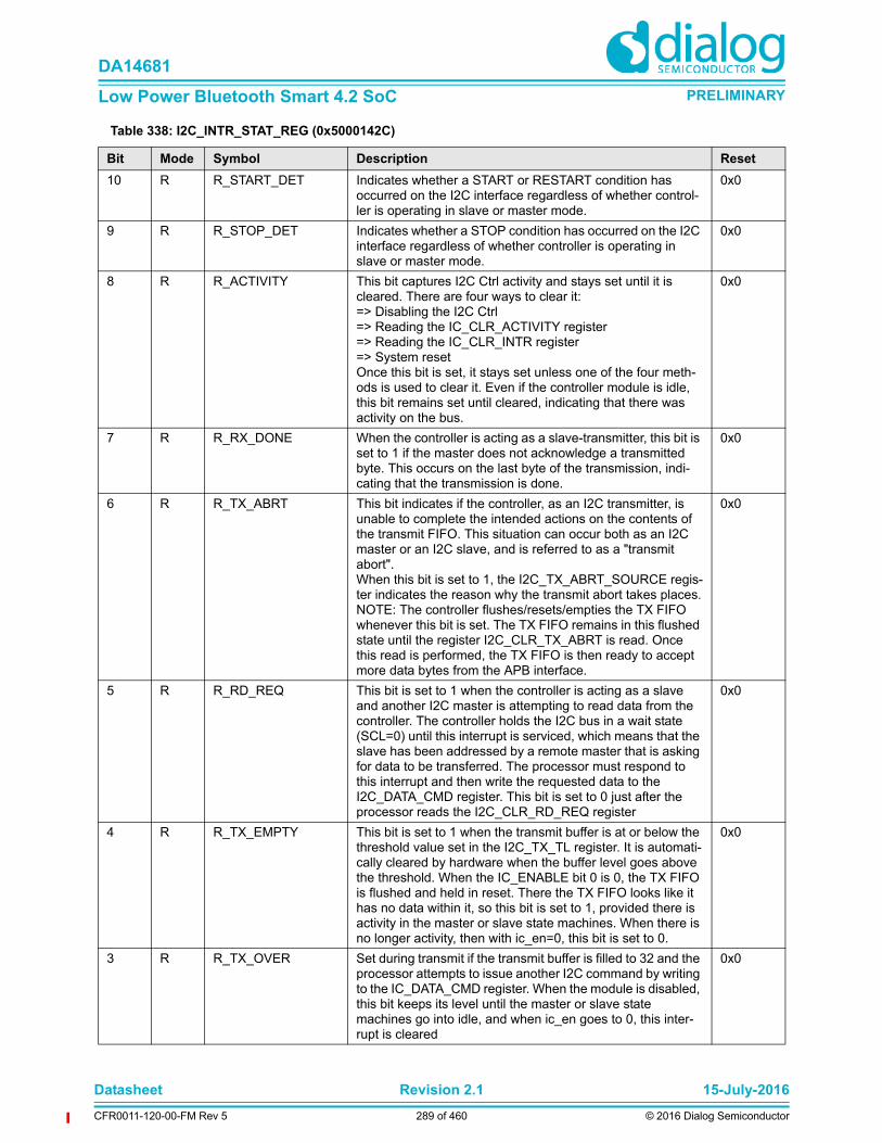
Datasheet Revision 2.1 15-July-2016
CFR0011-120-00-FM Rev 5 289 of 460 © 2016 Dialog Semiconductor
DA14681
Low Power Bluetooth Smart 4.2 SoC PRELIMINARY
10 R R_START_DET Indicates whether a START or RESTART condition has occurred on the I2C interface regardless of whether control-ler is operating in slave or master mode.
0x0
9 R R_STOP_DET Indicates whether a STOP condition has occurred on the I2C interface regardless of whether controller is operating in slave or master mode.
0x0
8 R R_ACTIVITY This bit captures I2C Ctrl activity and stays set until it is cleared. There are four ways to clear it:=> Disabling the I2C Ctrl=> Reading the IC_CLR_ACTIVITY register=> Reading the IC_CLR_INTR register=> System resetOnce this bit is set, it stays set unless one of the four meth-ods is used to clear it. Even if the controller module is idle, this bit remains set until cleared, indicating that there was activity on the bus.
0x0
7 R R_RX_DONE When the controller is acting as a slave-transmitter, this bit is set to 1 if the master does not acknowledge a transmitted byte. This occurs on the last byte of the transmission, indi-cating that the transmission is done.
0x0
6 R R_TX_ABRT This bit indicates if the controller, as an I2C transmitter, is unable to complete the intended actions on the contents of the transmit FIFO. This situation can occur both as an I2C master or an I2C slave, and is referred to as a "transmit abort".When this bit is set to 1, the I2C_TX_ABRT_SOURCE regis-ter indicates the reason why the transmit abort takes places.NOTE: The controller flushes/resets/empties the TX FIFO whenever this bit is set. The TX FIFO remains in this flushed state until the register I2C_CLR_TX_ABRT is read. Once this read is performed, the TX FIFO is then ready to accept more data bytes from the APB interface.
0x0
5 R R_RD_REQ This bit is set to 1 when the controller is acting as a slave and another I2C master is attempting to read data from the controller. The controller holds the I2C bus in a wait state (SCL=0) until this interrupt is serviced, which means that the slave has been addressed by a remote master that is asking for data to be transferred. The processor must respond to this interrupt and then write the requested data to the I2C_DATA_CMD register. This bit is set to 0 just after the processor reads the I2C_CLR_RD_REQ register
0x0
4 R R_TX_EMPTY This bit is set to 1 when the transmit buffer is at or below the threshold value set in the I2C_TX_TL register. It is automati-cally cleared by hardware when the buffer level goes above the threshold. When the IC_ENABLE bit 0 is 0, the TX FIFO is flushed and held in reset. There the TX FIFO looks like it has no data within it, so this bit is set to 1, provided there is activity in the master or slave state machines. When there is no longer activity, then with ic_en=0, this bit is set to 0.
0x0
3 R R_TX_OVER Set during transmit if the transmit buffer is filled to 32 and the processor attempts to issue another I2C command by writing to the IC_DATA_CMD register. When the module is disabled, this bit keeps its level until the master or slave state machines go into idle, and when ic_en goes to 0, this inter-rupt is cleared
0x0
Table 338: I2C_INTR_STAT_REG (0x5000142C)
Bit Mode Symbol Description Reset

Datasheet Revision 2.1 15-July-2016
CFR0011-120-00-FM Rev 5 290 of 460 © 2016 Dialog Semiconductor
DA14681
Low Power Bluetooth Smart 4.2 SoC PRELIMINARY
2 R R_RX_FULL Set when the receive buffer reaches or goes above the RX_TL threshold in the I2C_RX_TL register. It is automati-cally cleared by hardware when buffer level goes below the threshold. If the module is disabled (I2C_ENABLE[0]=0), the RX FIFO is flushed and held in reset; therefore the RX FIFO is not full. So this bit is cleared once the I2C_ENABLE bit 0 is programmed with a 0, regardless of the activity that contin-ues.
0x0
1 R R_RX_OVER Set if the receive buffer is completely filled to 32 and an addi-tional byte is received from an external I2C device. The con-troller acknowledges this, but any data bytes received after the FIFO is full are lost. If the module is disabled (I2C_ENABLE[0]=0), this bit keeps its level until the master or slave state machines go into idle, and when ic_en goes to 0, this interrupt is cleared.
0x0
0 R R_RX_UNDER Set if the processor attempts to read the receive buffer when it is empty by reading from the IC_DATA_CMD register. If the module is disabled (I2C_ENABLE[0]=0), this bit keeps its level until the master or slave state machines go into idle, and when ic_en goes to 0, this interrupt is cleared.
0x0
Table 338: I2C_INTR_STAT_REG (0x5000142C)
Bit Mode Symbol Description Reset
Table 339: I2C_INTR_MASK_REG (0x50001430)
Bit Mode Symbol Description Reset
15:12 - - Reserved 0x0
11 R/W M_GEN_CALL These bits mask their corresponding interrupt status bits in the I2C_INTR_STAT register.
0x1
10 R/W M_START_DET These bits mask their corresponding interrupt status bits in the I2C_INTR_STAT register.
0x0
9 R/W M_STOP_DET These bits mask their corresponding interrupt status bits in the I2C_INTR_STAT register.
0x0
8 R/W M_ACTIVITY These bits mask their corresponding interrupt status bits in the I2C_INTR_STAT register.
0x0
7 R/W M_RX_DONE These bits mask their corresponding interrupt status bits in the I2C_INTR_STAT register.
0x1
6 R/W M_TX_ABRT These bits mask their corresponding interrupt status bits in the I2C_INTR_STAT register.
0x1
5 R/W M_RD_REQ These bits mask their corresponding interrupt status bits in the I2C_INTR_STAT register.
0x1
4 R/W M_TX_EMPTY These bits mask their corresponding interrupt status bits in the I2C_INTR_STAT register.
0x1
3 R/W M_TX_OVER These bits mask their corresponding interrupt status bits in the I2C_INTR_STAT register.
0x1
2 R/W M_RX_FULL These bits mask their corresponding interrupt status bits in the I2C_INTR_STAT register.
0x1
1 R/W M_RX_OVER These bits mask their corresponding interrupt status bits in the I2C_INTR_STAT register.
0x1
0 R/W M_RX_UNDER These bits mask their corresponding interrupt status bits in the I2C_INTR_STAT register.
0x1

Datasheet Revision 2.1 15-July-2016
CFR0011-120-00-FM Rev 5 291 of 460 © 2016 Dialog Semiconductor
DA14681
Low Power Bluetooth Smart 4.2 SoC PRELIMINARY
Table 340: I2C_RAW_INTR_STAT_REG (0x50001434)
Bit Mode Symbol Description Reset
15:12 - - Reserved 0x0
11 R GEN_CALL Set only when a General Call address is received and it is acknowledged. It stays set until it is cleared either by disa-bling controller or when the CPU reads bit 0 of the I2C_CLR_GEN_CALL register. I2C Ctrl stores the received data in the Rx buffer.
0x0
10 R START_DET Indicates whether a START or RESTART condition has occurred on the I2C interface regardless of whether control-ler is operating in slave or master mode.
0x0
9 R STOP_DET Indicates whether a STOP condition has occurred on the I2C interface regardless of whether controller is operating in slave or master mode.
0x0
8 R ACTIVITY This bit captures I2C Ctrl activity and stays set until it is cleared. There are four ways to clear it:=> Disabling the I2C Ctrl=> Reading the IC_CLR_ACTIVITY register=> Reading the IC_CLR_INTR register=> System resetOnce this bit is set, it stays set unless one of the four meth-ods is used to clear it. Even if the controller module is idle, this bit remains set until cleared, indicating that there was activity on the bus.
0x0
7 R RX_DONE When the controller is acting as a slave-transmitter, this bit is set to 1 if the master does not acknowledge a transmitted byte. This occurs on the last byte of the transmission, indi-cating that the transmission is done.
0x0
6 R TX_ABRT This bit indicates if the controller, as an I2C transmitter, is unable to complete the intended actions on the contents of the transmit FIFO. This situation can occur both as an I2C master or an I2C slave, and is referred to as a "transmit abort".When this bit is set to 1, the I2C_TX_ABRT_SOURCE regis-ter indicates the reason why the transmit abort takes places.NOTE: The controller flushes/resets/empties the TX FIFO whenever this bit is set. The TX FIFO remains in this flushed state until the register I2C_CLR_TX_ABRT is read. Once this read is performed, the TX FIFO is then ready to accept more data bytes from the APB interface.
0x0
5 R RD_REQ This bit is set to 1 when I2C Ctrl is acting as a slave and another I2C master is attempting to read data from the con-troller. The controller holds the I2C bus in a wait state (SCL=0) until this interrupt is serviced, which means that the slave has been addressed by a remote master that is asking for data to be transferred. The processor must respond to this interrupt and then write the requested data to the I2C_DATA_CMD register. This bit is set to 0 just after the processor reads the I2C_CLR_RD_REQ register
0x0
4 R TX_EMPTY This bit is set to 1 when the transmit buffer is at or below the threshold value set in the I2C_TX_TL register. It is automati-cally cleared by hardware when the buffer level goes above the threshold. When the IC_ENABLE bit 0 is 0, the TX FIFO is flushed and held in reset. There the TX FIFO looks like it has no data within it, so this bit is set to 1, provided there is activity in the master or slave state machines. When there is no longer activity, then with ic_en=0, this bit is set to 0.
0x0

Datasheet Revision 2.1 15-July-2016
CFR0011-120-00-FM Rev 5 292 of 460 © 2016 Dialog Semiconductor
DA14681
Low Power Bluetooth Smart 4.2 SoC PRELIMINARY
3 R TX_OVER Set during transmit if the transmit buffer is filled to 32 and the processor attempts to issue another I2C command by writing to the IC_DATA_CMD register. When the module is disabled, this bit keeps its level until the master or slave state machines go into idle, and when ic_en goes to 0, this inter-rupt is cleared
0x0
2 R RX_FULL Set when the receive buffer reaches or goes above the RX_TL threshold in the I2C_RX_TL register. It is automati-cally cleared by hardware when buffer level goes below the threshold. If the module is disabled (I2C_ENABLE[0]=0), the RX FIFO is flushed and held in reset; therefore the RX FIFO is not full. So this bit is cleared once the I2C_ENABLE bit 0 is programmed with a 0, regardless of the activity that contin-ues.
0x0
1 R RX_OVER Set if the receive buffer is completely filled to 32 and an addi-tional byte is received from an external I2C device. The con-troller acknowledges this, but any data bytes received after the FIFO is full are lost. If the module is disabled (I2C_ENABLE[0]=0), this bit keeps its level until the master or slave state machines go into idle, and when ic_en goes to 0, this interrupt is cleared.
0x0
0 R RX_UNDER Set if the processor attempts to read the receive buffer when it is empty by reading from the IC_DATA_CMD register. If the module is disabled (I2C_ENABLE[0]=0), this bit keeps its level until the master or slave state machines go into idle, and when ic_en goes to 0, this interrupt is cleared.
0x0
Table 340: I2C_RAW_INTR_STAT_REG (0x50001434)
Bit Mode Symbol Description Reset
Table 341: I2C_RX_TL_REG (0x50001438)
Bit Mode Symbol Description Reset
15:5 - - Reserved 0x0
4:0 R/W RX_TL Receive FIFO Threshold Level Controls the level of entries (or above) that triggers the RX_FULL interrupt (bit 2 in I2C_RAW_INTR_STAT register). The valid range is 0-31, with the additional restriction that hardware does not allow this value to be set to a value larger than the depth of the buffer. If an attempt is made to do that, the actual value set will be the maximum depth of the buffer. A value of 0 sets the threshold for 1 entry, and a value of 31 sets the threshold for 32 entries.
0x0
Table 342: I2C_TX_TL_REG (0x5000143C)
Bit Mode Symbol Description Reset
15:5 - - Reserved 0x0
4:0 R/W RX_TL Transmit FIFO Threshold Level Controls the level of entries (or below) that trigger the TX_EMPTY interrupt (bit 4 in I2C_RAW_INTR_STAT register). The valid range is 0-31, with the additional restriction that it may not be set to value larger than the depth of the buffer. If an attempt is made to do that, the actual value set will be the maximum depth of the buffer. A value of 0 sets the threshold for 0 entries, and a value of 31 sets the threshold for 32 entries..
0x0

Datasheet Revision 2.1 15-July-2016
CFR0011-120-00-FM Rev 5 293 of 460 © 2016 Dialog Semiconductor
DA14681
Low Power Bluetooth Smart 4.2 SoC PRELIMINARY
Table 343: I2C_CLR_INTR_REG (0x50001440)
Bit Mode Symbol Description Reset
15:1 - - Reserved 0x0
0 R CLR_INTR Read this register to clear the combined interrupt, all individ-ual interrupts, and the I2C_TX_ABRT_SOURCE register. This bit does not clear hardware clearable interrupts but soft-ware clearable interrupts. Refer to Bit 9 of the I2C_TX_ABRT_SOURCE register for an exception to clear-ing I2C_TX_ABRT_SOURCE
0x0
Table 344: I2C_CLR_RX_UNDER_REG (0x50001444)
Bit Mode Symbol Description Reset
15:1 - - Reserved 0x0
0 R CLR_RX_UNDER Read this register to clear the RX_UNDER interrupt (bit 0) of theI2C_RAW_INTR_STAT register.
0x0
Table 345: I2C_CLR_RX_OVER_REG (0x50001448)
Bit Mode Symbol Description Reset
15:1 - - Reserved 0x0
0 R CLR_RX_OVER Read this register to clear the RX_OVER interrupt (bit 1) of theI2C_RAW_INTR_STAT register.
0x0
Table 346: I2C_CLR_TX_OVER_REG (0x5000144C)
Bit Mode Symbol Description Reset
15:1 - - Reserved 0x0
0 R CLR_TX_OVER Read this register to clear the TX_OVER interrupt (bit 3) of the I2C_RAW_INTR_STAT register.
0x0
Table 347: I2C_CLR_RD_REQ_REG (0x50001450)
Bit Mode Symbol Description Reset
15:1 - - Reserved 0x0
0 R CLR_RD_REQ Read this register to clear the RD_REQ interrupt (bit 5) of the I2C_RAW_INTR_STAT register.
0x0
Table 348: I2C_CLR_TX_ABRT_REG (0x50001454)
Bit Mode Symbol Description Reset
15:1 - - Reserved 0x0
0 R CLR_TX_ABRT Read this register to clear the TX_ABRT interrupt (bit 6) of theIC_RAW_INTR_STAT register, and the I2C_TX_ABRT_SOURCE register. This also releases the TX FIFO from the flushed/reset state, allowing more writes to the TX FIFO. Refer to Bit 9 of the I2C_TX_ABRT_SOURCE register for an exception to clearing IC_TX_ABRT_SOURCE.
0x0

Datasheet Revision 2.1 15-July-2016
CFR0011-120-00-FM Rev 5 294 of 460 © 2016 Dialog Semiconductor
DA14681
Low Power Bluetooth Smart 4.2 SoC PRELIMINARY
Table 349: I2C_CLR_RX_DONE_REG (0x50001458)
Bit Mode Symbol Description Reset
15:1 - - Reserved 0x0
0 R CLR_RX_DONE Read this register to clear the RX_DONE interrupt (bit 7) of theI2C_RAW_INTR_STAT register.
0x0
Table 350: I2C_CLR_ACTIVITY_REG (0x5000145C)
Bit Mode Symbol Description Reset
15:1 - - Reserved 0x0
0 R CLR_ACTIVITY Reading this register clears the ACTIVITY interrupt if the I2C is not active anymore. If the I2C module is still active on the bus, the ACTIVITY interrupt bit continues to be set. It is auto-matically cleared by hardware if the module is disabled and if there is no further activity on the bus. The value read from this register to get status of the ACTIVITY interrupt (bit 8) of the IC_RAW_INTR_STAT register
0x0
Table 351: I2C_CLR_STOP_DET_REG (0x50001460)
Bit Mode Symbol Description Reset
15:1 - - Reserved 0x0
0 R CLR_ACTIVITY Reading this register clears the ACTIVITY interrupt if the I2C is not active anymore. If the I2C module is still active on the bus, the ACTIVITY interrupt bit continues to be set. It is auto-matically cleared by hardware if the module is disabled and if there is no further activity on the bus. The value read from this register to get status of the ACTIVITY interrupt (bit 8) of the IC_RAW_INTR_STAT register.
0x0
Table 352: I2C_CLR_START_DET_REG (0x50001464)
Bit Mode Symbol Description Reset
15:1 - - Reserved 0x0
0 R CLR_START_DET Read this register to clear the START_DET interrupt (bit 10) of the IC_RAW_INTR_STAT register.
0x0
Table 353: I2C_CLR_GEN_CALL_REG (0x50001468)
Bit Mode Symbol Description Reset
15:1 - - Reserved 0x0
0 R CLR_GEN_CALL Read this register to clear the GEN_CALL interrupt (bit 11) ofI2C_RAW_INTR_STAT register.
0x0
Table 354: I2C_ENABLE_REG (0x5000146C)
Bit Mode Symbol Description Reset
15:1 - - Reserved 0x0

Datasheet Revision 2.1 15-July-2016
CFR0011-120-00-FM Rev 5 295 of 460 © 2016 Dialog Semiconductor
DA14681
Low Power Bluetooth Smart 4.2 SoC PRELIMINARY
0 R/W CTRL_ENABLE Controls whether the controller is enabled.0: Disables the controller (TX and RX FIFOs are held in an erased state)1: Enables the controllerSoftware can disable the controller while it is active. How-ever, it is important that care be taken to ensure that the con-troller is disabled properly. When the controller is disabled, the following occurs:* The TX FIFO and RX FIFO get flushed.* Status bits in the IC_INTR_STAT register are still active until the controller goes into IDLE state.If the module is transmitting, it stops as well as deletes the contents of the transmit buffer after the current transfer is complete. If the module is receiving, the controller stops the current transfer at the end of the current byte and does not acknowledge the transfer.There is a two ic_clk delay when enabling or disabling the controller
0x0
Table 354: I2C_ENABLE_REG (0x5000146C)
Bit Mode Symbol Description Reset
Table 355: I2C_STATUS_REG (0x50001470)
Bit Mode Symbol Description Reset
15:7 - - Reserved 0x0
6 R SLV_ACTIVITY Slave FSM Activity Status. When the Slave Finite State Machine (FSM) is not in the IDLE state, this bit is set.0: Slave FSM is in IDLE state so the Slave part of the con-troller is not Active1: Slave FSM is not in IDLE state so the Slave part of the controller is Active
0x0
5 R MST_ACTIVITY Master FSM Activity Status. When the Master Finite State Machine (FSM) is not in the IDLE state, this bit is set.0: Master FSM is in IDLE state so the Master part of the con-troller is not Active1: Master FSM is not in IDLE state so the Master part of the controller is Active
0x0
4 R RFF Receive FIFO Completely Full. When the receive FIFO is completely full, this bit is set. When the receive FIFO con-tains one or more empty location, this bit is cleared.0: Receive FIFO is not full1: Receive FIFO is full
0x0
3 R RFNE Receive FIFO Not Empty. This bit is set when the receive FIFO contains one or more entries; it is cleared when the receive FIFO is empty.0: Receive FIFO is empty1: Receive FIFO is not empty
0x0
2 R TFE Transmit FIFO Completely Empty. When the transmit FIFO is completely empty, this bit is set. When it contains one or more valid entries, this bit is cleared. This bit field does not request an interrupt.0: Transmit FIFO is not empty1: Transmit FIFO is empty
0x1
1 R TFNF Transmit FIFO Not Full. Set when the transmit FIFO contains one or more empty locations, and is cleared when the FIFO is full.0: Transmit FIFO is full1: Transmit FIFO is not full
0x1

Datasheet Revision 2.1 15-July-2016
CFR0011-120-00-FM Rev 5 296 of 460 © 2016 Dialog Semiconductor
DA14681
Low Power Bluetooth Smart 4.2 SoC PRELIMINARY
0 R I2C_ACTIVITY I2C Activity Status. 0x0
Table 355: I2C_STATUS_REG (0x50001470)
Bit Mode Symbol Description Reset
Table 356: I2C_TXFLR_REG (0x50001474)
Bit Mode Symbol Description Reset
15:6 - - Reserved 0x0
5:0 R TXFLR Transmit FIFO Level. Contains the number of valid data entries in the transmit FIFO. Size is constrained by the TXFLR value
0x0
Table 357: I2C_RXFLR_REG (0x50001478)
Bit Mode Symbol Description Reset
15:6 - - Reserved 0x0
5:0 R RXFLR Receive FIFO Level. Contains the number of valid data entries in the receive FIFO. Size is constrained by the RXFLR value
0x0
Table 358: I2C_SDA_HOLD_REG (0x5000147C)
Bit Mode Symbol Description Reset
15:0 R/W IC_SDA_HOLD SDA Hold time 0x1
Table 359: I2C_TX_ABRT_SOURCE_REG (0x50001480)
Bit Mode Symbol Description Reset
15 R ABRT_SLVRD_INTX 1: When the processor side responds to a slave mode request for data to be transmitted to a remote master and user writes a 1 in CMD (bit 8) of 2IC_DATA_CMD register
0x0
14 R ABRT_SLV_ARBLOST
1: Slave lost the bus while transmitting data to a remote master.I2C_TX_ABRT_SOURCE[12] is set at the same time. Note: Even though the slave never "owns" the bus, something could go wrong on the bus. This is a fail safe check. For instance, during a data transmission at the low-to-high tran-sition of SCL, if what is on the data bus is not what is sup-posed to be transmitted, then the controller no longer own the bus.
0x0
13 R ABRT_SLVFLUSH_TXFIFO
1: Slave has received a read command and some data exists in the TX FIFO so the slave issues a TX_ABRT inter-rupt to flush old data in TX FIFO.
0x0
12 R ARB_LOST 1: Master has lost arbitration, or if I2C_TX_ABRT_SOURCE[14] is also set, then the slave transmitter has lost arbitration. Note: I2C can be both master and slave at the same time.
0x0
11 R ABRT_MASTER_DIS 1: User tries to initiate a Master operation with the Master mode disabled.
0x0
10 R ABRT_10B_RD_NORSTRT
1: The restart is disabled (IC_RESTART_EN bit (I2C_CON[5]) = 0) and the master sends a read command in 10-bit addressing mode.
0x0

Datasheet Revision 2.1 15-July-2016
CFR0011-120-00-FM Rev 5 297 of 460 © 2016 Dialog Semiconductor
DA14681
Low Power Bluetooth Smart 4.2 SoC PRELIMINARY
9 R ABRT_SBYTE_NORSTRT
To clear Bit 9, the source of the ABRT_SBYTE_NORSTRT must be fixed first; restart must be enabled (I2C_CON[5]=1), the SPECIAL bit must be cleared (I2C_TAR[11]), or the GC_OR_START bit must be cleared (I2C_TAR[10]). Once the source of the ABRT_SBYTE_NORSTRT is fixed, then this bit can be cleared in the same manner as other bits in this register. If the source of the ABRT_SBYTE_NORSTRT is not fixed before attempting to clear this bit, bit 9 clears for one cycle and then gets re-asserted. 1: The restart is disa-bled (IC_RESTART_EN bit (I2C_CON[5]) = 0) and the user is trying to send a START Byte.
0x0
8 R ABRT_HS_NORSTRT
1: The restart is disabled (IC_RESTART_EN bit (I2C_CON[5]) = 0) and the user is trying to use the master to transfer data in High Speed mode
0x0
7 R ABRT_SBYTE_ACKDET
1: Master has sent a START Byte and the START Byte was acknowledged (wrong behavior).
0x0
6 R ABRT_HS_ACKDET 1: Master is in High Speed mode and the High Speed Master code was acknowledged (wrong behavior).
0x0
5 R ABRT_GCALL_READ
1: the controller in master mode sent a General Call but the user programmed the byte following the General Call to be a read from the bus (IC_DATA_CMD[9] is set to 1).
0x0
4 R ABRT_GCALL_NOACK
1: the controller in master mode sent a General Call and no slave on the bus acknowledged the General Call.
0x0
3 R ABRT_TXDATA_NOACK
1: This is a master-mode only bit. Master has received an acknowledgement for the address, but when it sent data byte(s) following the address, it did not receive an acknowl-edge from the remote slave(s).
0x0
2 R ABRT_10ADDR2_NOACK
1: Master is in 10-bit address mode and the second address byte of the 10-bit address was not acknowledged by any slave.
0x0
1 R ABRT_10ADDR1_NOACK
1: Master is in 10-bit address mode and the first 10-bit address byte was not acknowledged by any slave.
0x0
0 R ABRT_7B_ADDR_NOACK
1: Master is in 7-bit addressing mode and the address sent was not acknowledged by any slave.
0x0
Table 359: I2C_TX_ABRT_SOURCE_REG (0x50001480)
Bit Mode Symbol Description Reset
Table 360: I2C_DMA_CR_REG (0x50001488)
Bit Mode Symbol Description Reset
1 R/W TDMAE Transmit DMA Enable. //This bit enables/disables the trans-mit FIFO DMA channel. 0 = Transmit DMA disabled 1 = Transmit DMA enabled
0x0
0 R/W RDMAE Receive DMA Enable. This bit enables/disables the receive FIFO DMA channel. 0 = Receive DMA disabled 1 = Receive DMA enabled
0x0
Table 361: I2C_DMA_TDLR_REG (0x5000148C)
Bit Mode Symbol Description Reset
4:0 R/W DMATDL Transmit Data Level. This bit field controls the level at which a DMA request is made by the transmit logic. It is equal to the watermark level; that is, the dma_tx_req signal is gener-ated when the number of valid data entries in the transmit FIFO is equal to or below this field value, and TDMAE = 1.
0x0

Datasheet Revision 2.1 15-July-2016
CFR0011-120-00-FM Rev 5 298 of 460 © 2016 Dialog Semiconductor
DA14681
Low Power Bluetooth Smart 4.2 SoC PRELIMINARY
Table 362: I2C_DMA_RDLR_REG (0x50001490)
Bit Mode Symbol Description Reset
4:0 R/W DMARDL Receive Data Level. This bit field controls the level at which a DMA request is made by the receive logic. The watermark level = DMARDL+1; that is, dma_rx_req is generated when the number of valid data entries in the receive FIFO is equal to or more than this field value + 1, and RDMAE =1. For instance, when DMARDL is 0, then dma_rx_req is asserted when 1 or more data entries are present in the receive FIFO.
0x0
Table 363: I2C_SDA_SETUP_REG (0x50001494)
Bit Mode Symbol Description Reset
15:8 - - Reserved 0x0
7:0 R/W SDA_SETUP SDA Setup.This register controls the amount of time delay (number of I2C clock periods) between the rising edge of SCL and SDA changing by holding SCL low when I2C block services a read request while operating as a slave-transmitter. The rele-vant I2C requirement is tSU:DAT (note 4) as detailed in the I2C Bus Specification. This register must be programmed with a value equal to or greater than 2.It is recommended that if the required delay is 1000ns, then for an I2C frequency of 10 MHz, IC_SDA_SETUP should be programmed to a value of 11.Writes to this register succeed only when IC_ENABLE[0] = 0.
0x64
Table 364: I2C_ACK_GENERAL_CALL_REG (0x50001498)
Bit Mode Symbol Description Reset
15:1 - - Reserved 0x0
0 R/W ACK_GEN_CALL ACK General Call. When set to 1, I2C Ctrl responds with a ACK (by asserting ic_data_oe) when it receives a General Call. When set to 0, the controller does not generate General Call interrupts.
0x0
Table 365: I2C_ENABLE_STATUS_REG (0x5000149C)
Bit Mode Symbol Description Reset
15:3 - - Reserved 0x0

Datasheet Revision 2.1 15-July-2016
CFR0011-120-00-FM Rev 5 299 of 460 © 2016 Dialog Semiconductor
DA14681
Low Power Bluetooth Smart 4.2 SoC PRELIMINARY
2 R SLV_RX_DATA_LOST
Slave Received Data Lost. This bit indicates if a Slave-Receiveroperation has been aborted with at least one data byte received from an I2C transfer due to the setting of IC_ENABLE from 1 to 0. When read as 1, the controller is deemed to have been actively engaged in an aborted I2C transfer (with matching address) and the data phase of the I2C transfer has been entered, even though a data byte has been responded with a NACK. NOTE: If the remote I2C mas-ter terminates the transfer with a STOP condition before the controller has a chance to NACK a transfer, and IC_ENABLE has been set to 0, then this bit is also set to 1.When read as 0, the controller is deemed to have been disa-bled without being actively involved in the data phase of a Slave-Receiver transfer.NOTE: The CPU can safely read this bit when IC_EN (bit 0) is read as 0.
0x0
1 R SLV_DISABLED_WHILE_BUSY
Slave Disabled While Busy (Transmit, Receive). This bit indi-cates if a potential or active Slave operation has been aborted due to the setting of the IC_ENABLE register from 1 to 0. This bit is set when the CPU writes a 0 to the IC_ENABLE register while:(a) I2C Ctrl is receiving the address byte of the Slave-Trans-mitter operation from a remote master; OR,(b) address and data bytes of the Slave-Receiver operation from a remote master. When read as 1, the controller is deemed to have forced a NACK during any part of an I2C transfer, irrespective of whether the I2C address matches the slave address set in I2C Ctrl (IC_SAR register) OR if the transfer is completed before IC_ENABLE is set to 0 but has not taken effect.NOTE: If the remote I2C master terminates the transfer with a STOP condition before the the controller has a chance to NACK a transfer, and IC_ENABLE has been set to 0, then this bit will also be set to 1.When read as 0, the controller is deemed to have been disa-bled when there is master activity, or when the I2C bus is idle.NOTE: The CPU can safely read this bit when IC_EN (bit 0) is read as 0.
0x0
0 R IC_EN ic_en Status. This bit always reflects the value driven on the output port ic_en. When read as 1, the controller is deemed to be in an enabled state.When read as 0, the controller is deemed completely inac-tive.NOTE: The CPU can safely read this bit anytime. When this bit is read as 0, the CPU can safely read SLV_RX_DATA_LOST (bit 2) and SLV_DISABLED_WHILE_BUSY (bit 1).
0x0
Table 365: I2C_ENABLE_STATUS_REG (0x5000149C)
Bit Mode Symbol Description Reset
Table 366: I2C_IC_FS_SPKLEN_REG (0x500014A0)
Bit Mode Symbol Description Reset
15:8 - - Reserved 0x0

Datasheet Revision 2.1 15-July-2016
CFR0011-120-00-FM Rev 5 300 of 460 © 2016 Dialog Semiconductor
DA14681
Low Power Bluetooth Smart 4.2 SoC PRELIMINARY
7:0 R/W IC_FS_SPKLEN This register must be set before any I2C bus transaction can take place to ensure stable operation. This register sets the duration, measured in ic_clk cycles, of the longest spike in the SCL or SDA lines that will be filtered out by the spike suppression logic. This register can be written only when the I2C interface is disabled which corresponds to the IC_ENABLE register being set to 0. Writes at other times have no effect. The minimum valid value is 2; hardware pre-vents values less than this being written, and if attempted results in 2 being set.
0x1
Table 366: I2C_IC_FS_SPKLEN_REG (0x500014A0)
Bit Mode Symbol Description Reset
Table 367: I2C_COMP_PARAM1_REG (0x500014F4)
Bit Mode Symbol Description Reset
- - - Undefined -
Table 368: I2C_COMP_PARAM2_REG (0x500014F6)
Bit Mode Symbol Description Reset
- - - Undefined -
Table 369: I2C_COMP_VERSION_REG (0x500014F8)
Bit Mode Symbol Description Reset
- - - Undefined -
Table 370: I2C_COMP2_VERSION (0x500014FA)
Bit Mode Symbol Description Reset
- - - Undefined -
Table 371: I2C_COMP_TYPE_REG (0x500014FC)
Bit Mode Symbol Description Reset
- - - Undefined -
Table 372: I2C_COMP_TYPE2_REG (0x500014FE)
Bit Mode Symbol Description Reset
- - - Undefined -
Table 373: I2C2_CON_REG (0x50001500)
Bit Mode Symbol Description Reset
15:7 - - Reserved 0x0
6 R/W I2C_SLAVE_DISABLE
Slave enabled or disabled after reset is applied, which means software does not have to configure the slave.0=slave is enabled1=slave is disabledSoftware should ensure that if this bit is written with '0', then bit 0 should also be written with a '0'.
0x1

Datasheet Revision 2.1 15-July-2016
CFR0011-120-00-FM Rev 5 301 of 460 © 2016 Dialog Semiconductor
DA14681
Low Power Bluetooth Smart 4.2 SoC PRELIMINARY
5 R/W I2C_RESTART_EN Determines whether RESTART conditions may be sent when acting as a master0= disable1=enable
0x1
4 R/W I2C_10BITADDR_MASTER
Controls whether the controller starts its transfers in 7- or 10-bit addressing mode when acting as a master.0= 7-bit addressing1= 10-bit addressing
0x1
3 R/W I2C_10BITADDR_SLAVE
When acting as a slave, this bit controls whether the control-ler responds to 7- or 10-bit addresses.0= 7-bit addressing1= 10-bit addressing
0x1
2:1 R/W I2C_SPEED These bits control at which speed the controller operates.1= standard mode (100 kbit/s)2= fast mode (400 kbit/s)
0x2
0 R/W I2C_MASTER_MODE
This bit controls whether the controller master is enabled.0= master disabled1= master enabledSoftware should ensure that if this bit is written with '1' then bit 6 should also be written with a '1'.
0x1
Table 373: I2C2_CON_REG (0x50001500)
Bit Mode Symbol Description Reset
Table 374: I2C2_TAR_REG (0x50001504)
Bit Mode Symbol Description Reset
15:12 - - Reserved 0x0
11 R/W SPECIAL This bit indicates whether software performs a General Call orSTART BYTE command.0: ignore bit 10 GC_OR_START and use IC_TAR normally1: perform special I2C command as specified in GC_OR_STARTbit
0x0
10 R/W GC_OR_START If bit 11 (SPECIAL) is set to 1, then this bit indicates whether a General Call or START byte command is to be performed by the controller.0: General Call Address - after issuing a General Call, only writes may be performed. Attempting to issue a read com-mand results in setting bit 6 (TX_ABRT) of the IC_RAW_INTR_STAT register. The controller remains in General Call mode until the SPECIAL bit value (bit 11) is cleared.1: START BYTE
0x0
9:0 R/W IC_TAR This is the target address for any master transaction. When transmitting a General Call, these bits are ignored. To gener-ate a START BYTE, the CPU needs to write only once into these bits.Note: If the IC_TAR and IC_SAR are the same, loopback exists but the FIFOs are shared between master and slave, so full loopback is not feasible. Only one direction loopback mode is supported (simplex), not duplex. A master cannot transmit to itself; it can transmit to only a slaveWrites to this register succeed only when IC_ENABLE[0] is set to 0
0x55

Datasheet Revision 2.1 15-July-2016
CFR0011-120-00-FM Rev 5 302 of 460 © 2016 Dialog Semiconductor
DA14681
Low Power Bluetooth Smart 4.2 SoC PRELIMINARY
Table 375: I2C2_SAR_REG (0x50001508)
Bit Mode Symbol Description Reset
15:10 - - Reserved 0x0
9:0 R/W IC_SAR The IC_SAR holds the slave address when the I2C is operat-ing as a slave. For 7-bit addressing, only IC_SAR[6:0] is used. This register can be written only when the I2C inter-face is disabled, which corresponds to the IC_ENABLE reg-ister being set to 0. Writes at other times have no effect.
0x55
Table 376: I2C2_HS_MADDR_REG (0x5000150C)
Bit Mode Symbol Description Reset
2:0 R/W IIC_HS_MAR This bit field holds the value of the I2C HS mode master code.
0x1
Table 377: I2C2_DATA_CMD_REG (0x50001510)
Bit Mode Symbol Description Reset
15:9 - - Reserved 0x0
8 R/W CMD This bit controls whether a read or a write is performed. This bit does not control the direction when the I2C Ctrl acts as a slave. It controls only the direction when it acts as a master.1 = Read0 = WriteWhen a command is entered in the TX FIFO, this bit distin-guishes the write and read commands. In slave-receiver mode, this bit is a "don't care" because writes to this register are not required. In slave-transmitter mode, a "0" indicates that CPU data is to be transmitted and as DAT or IC_DATA_CMD[7:0]. When programming this bit, you should remember the following: attempting to perform a read opera-tion after a General Call command has been sent results in a TX_ABRT interrupt (bit 6 of the I2C_RAW_INTR_STAT_REG), unless bit 11 (SPECIAL) in the I2C_TAR register has been cleared.If a "1" is written to this bit after receiving a RD_REQ inter-rupt, then a TX_ABRT interrupt occurs.NOTE: It is possible that while attempting a master I2C read transfer on the controller, a RD_REQ interrupt may have occurred simultaneously due to a remote I2C master addressing the controller. In this type of scenario, it ignores the I2C_DATA_CMD write, generates a TX_ABRT interrupt, and waits to service the RD_REQ interrupt
0x0
7:0 R/W DAT This register contains the data to be transmitted or received on the I2C bus. If you are writing to this register and want to perform a read, bits 7:0 (DAT) are ignored by the controller. However, when you read this register, these bits return the value of data received on the controller's interface.
0x0

Datasheet Revision 2.1 15-July-2016
CFR0011-120-00-FM Rev 5 303 of 460 © 2016 Dialog Semiconductor
DA14681
Low Power Bluetooth Smart 4.2 SoC PRELIMINARY
Table 378: I2C2_SS_SCL_HCNT_REG (0x50001514)
Bit Mode Symbol Description Reset
15:0 R/W IC_SS_SCL_HCNT This register must be set before any I2C bus transaction can take place to ensure proper I/O timing. This register sets the SCL clock high-period count for standard speed. This regis-ter can be written only when the I2C interface is disabled which corresponds to the IC_ENABLE register being set to 0. Writes at othertimes have no effect.The minimum valid value is 6; hardware prevents values less than this being written, and if attempted results in 6 being set.NOTE: This register must not be programmed to a value higher than 65525, because the controller uses a 16-bit counter to flag an I2C bus idle condition when this counter reaches a value of IC_SS_SCL_HCNT + 10.
0x48
Table 379: I2C2_SS_SCL_LCNT_REG (0x50001518)
Bit Mode Symbol Description Reset
15:0 R/W IC_SS_SCL_LCNT This register must be set before any I2C bus transaction can take place to ensure proper I/O timing. This register sets the SCL clock low period count for standard speed.This register can be written only when the I2C interface is disabled which corresponds to the I2C_ENABLE register being set to 0. Writes at other times have no effect.The minimum valid value is 8; hardware prevents values less than this being written, and if attempted, results in 8 being set.
0x4F
Table 380: I2C2_FS_SCL_HCNT_REG (0x5000151C)
Bit Mode Symbol Description Reset
15:0 R/W IC_FS_SCL_HCNT This register must be set before any I2C bus transaction can take place to ensure proper I/O timing. This register sets the SCL clock high-period count for fast speed. It is used in high-speed mode to send the Master Code and START BYTE or General CALL. This register can be written only when the I2C interface is disabled, which corresponds to the I2C_ENABLE register being set to 0. Writes at other times have no effect.The minimum valid value is 6; hardware prevents values less than this being written, and if attempted results in 6 being set.
0x8

Datasheet Revision 2.1 15-July-2016
CFR0011-120-00-FM Rev 5 304 of 460 © 2016 Dialog Semiconductor
DA14681
Low Power Bluetooth Smart 4.2 SoC PRELIMINARY
Table 381: I2C2_FS_SCL_LCNT_REG (0x50001520)
Bit Mode Symbol Description Reset
15:0 R/W IC_FS_SCL_LCNT This register must be set before any I2C bus transaction can take place to ensure proper I/O timing. This register sets the SCL clock low-period count for fast speed. It is used in high-speed mode to send the Master Code and START BYTE or General CALL. This register can be written only when the I2C interface is disabled, which corresponds to the I2C_ENABLE register being set to 0. Writes at other times have no effect.The minimum valid value is 8; hardware prevents values less than this being written, and if attempted results in 8 being set. For designs with APB_DATA_WIDTH = 8 the order of programming is important to ensure the correct operation of the controller. The lower byte must be programmed first. Then the upper byte is programmed.
0x17
Table 382: I2C2_INTR_STAT_REG (0x5000152C)
Bit Mode Symbol Description Reset
15:12 - - Reserved 0x0
11 R R_GEN_CALL Set only when a General Call address is received and it is acknowledged. It stays set until it is cleared either by disa-bling controller or when the CPU reads bit 0 of the I2C_CLR_GEN_CALL register. The controller stores the received data in the Rx buffer.
0x0
10 R R_START_DET Indicates whether a START or RESTART condition has occurred on the I2C interface regardless of whether control-ler is operating in slave or master mode.
0x0
9 R R_STOP_DET Indicates whether a STOP condition has occurred on the I2C interface regardless of whether controller is operating in slave or master mode.
0x0
8 R R_ACTIVITY This bit captures I2C Ctrl activity and stays set until it is cleared. There are four ways to clear it:=> Disabling the I2C Ctrl=> Reading the IC_CLR_ACTIVITY register=> Reading the IC_CLR_INTR register=> System resetOnce this bit is set, it stays set unless one of the four meth-ods is used to clear it. Even if the controller module is idle, this bit remains set until cleared, indicating that there was activity on the bus.
0x0
7 R R_RX_DONE When the controller is acting as a slave-transmitter, this bit is set to 1 if the master does not acknowledge a transmitted byte. This occurs on the last byte of the transmission, indi-cating that the transmission is done.
0x0

Datasheet Revision 2.1 15-July-2016
CFR0011-120-00-FM Rev 5 305 of 460 © 2016 Dialog Semiconductor
DA14681
Low Power Bluetooth Smart 4.2 SoC PRELIMINARY
6 R R_TX_ABRT This bit indicates if the controller, as an I2C transmitter, is unable to complete the intended actions on the contents of the transmit FIFO. This situation can occur both as an I2C master or an I2C slave, and is referred to as a "transmit abort".When this bit is set to 1, the I2C_TX_ABRT_SOURCE regis-ter indicates the reason why the transmit abort takes places.NOTE: The controller flushes/resets/empties the TX FIFO whenever this bit is set. The TX FIFO remains in this flushed state until the register I2C_CLR_TX_ABRT is read. Once this read is performed, the TX FIFO is then ready to accept more data bytes from the APB interface.
0x0
5 R R_RD_REQ This bit is set to 1 when the controller is acting as a slave and another I2C master is attempting to read data from the controller. The controller holds the I2C bus in a wait state (SCL=0) until this interrupt is serviced, which means that the slave has been addressed by a remote master that is asking for data to be transferred. The processor must respond to this interrupt and then write the requested data to the I2C_DATA_CMD register. This bit is set to 0 just after the processor reads the I2C_CLR_RD_REQ register
0x0
4 R R_TX_EMPTY This bit is set to 1 when the transmit buffer is at or below the threshold value set in the I2C_TX_TL register. It is automati-cally cleared by hardware when the buffer level goes above the threshold. When the IC_ENABLE bit 0 is 0, the TX FIFO is flushed and held in reset. There the TX FIFO looks like it has no data within it, so this bit is set to 1, provided there is activity in the master or slave state machines. When there is no longer activity, then with ic_en=0, this bit is set to 0.
0x0
3 R R_TX_OVER Set during transmit if the transmit buffer is filled to 32 and the processor attempts to issue another I2C command by writing to the IC_DATA_CMD register. When the module is disabled, this bit keeps its level until the master or slave state machines go into idle, and when ic_en goes to 0, this inter-rupt is cleared
0x0
2 R R_RX_FULL Set when the receive buffer reaches or goes above the RX_TL threshold in the I2C_RX_TL register. It is automati-cally cleared by hardware when buffer level goes below the threshold. If the module is disabled (I2C_ENABLE[0]=0), the RX FIFO is flushed and held in reset; therefore the RX FIFO is not full. So this bit is cleared once the I2C_ENABLE bit 0 is programmed with a 0, regardless of the activity that contin-ues.
0x0
1 R R_RX_OVER Set if the receive buffer is completely filled to 32 and an addi-tional byte is received from an external I2C device. The con-troller acknowledges this, but any data bytes received after the FIFO is full are lost. If the module is disabled (I2C_ENABLE[0]=0), this bit keeps its level until the master or slave state machines go into idle, and when ic_en goes to 0, this interrupt is cleared.
0x0
0 R R_RX_UNDER Set if the processor attempts to read the receive buffer when it is empty by reading from the IC_DATA_CMD register. If the module is disabled (I2C_ENABLE[0]=0), this bit keeps its level until the master or slave state machines go into idle, and when ic_en goes to 0, this interrupt is cleared.
0x0
Table 382: I2C2_INTR_STAT_REG (0x5000152C)
Bit Mode Symbol Description Reset

Datasheet Revision 2.1 15-July-2016
CFR0011-120-00-FM Rev 5 306 of 460 © 2016 Dialog Semiconductor
DA14681
Low Power Bluetooth Smart 4.2 SoC PRELIMINARY
Table 383: I2C2_INTR_MASK_REG (0x50001530)
Bit Mode Symbol Description Reset
15:12 - - Reserved 0x0
11 R/W M_GEN_CALL These bits mask their corresponding interrupt status bits in the I2C_INTR_STAT register.
0x1
10 R/W M_START_DET These bits mask their corresponding interrupt status bits in the I2C_INTR_STAT register.
0x0
9 R/W M_STOP_DET These bits mask their corresponding interrupt status bits in the I2C_INTR_STAT register.
0x0
8 R/W M_ACTIVITY These bits mask their corresponding interrupt status bits in the I2C_INTR_STAT register.
0x0
7 R/W M_RX_DONE These bits mask their corresponding interrupt status bits in the I2C_INTR_STAT register.
0x1
6 R/W M_TX_ABRT These bits mask their corresponding interrupt status bits in the I2C_INTR_STAT register.
0x1
5 R/W M_RD_REQ These bits mask their corresponding interrupt status bits in the I2C_INTR_STAT register.
0x1
4 R/W M_TX_EMPTY These bits mask their corresponding interrupt status bits in the I2C_INTR_STAT register.
0x1
3 R/W M_TX_OVER These bits mask their corresponding interrupt status bits in the I2C_INTR_STAT register.
0x1
2 R/W M_RX_FULL These bits mask their corresponding interrupt status bits in the I2C_INTR_STAT register.
0x1
1 R/W M_RX_OVER These bits mask their corresponding interrupt status bits in the I2C_INTR_STAT register.
0x1
0 R/W M_RX_UNDER These bits mask their corresponding interrupt status bits in the I2C_INTR_STAT register.
0x1
Table 384: I2C2_RAW_INTR_STAT_REG (0x50001534)
Bit Mode Symbol Description Reset
15:12 - - Reserved 0x0
11 R GEN_CALL Set only when a General Call address is received and it is acknowledged. It stays set until it is cleared either by disa-bling controller or when the CPU reads bit 0 of the I2C_CLR_GEN_CALL register. I2C Ctrl stores the received data in the Rx buffer.
0x0
10 R START_DET Indicates whether a START or RESTART condition has occurred on the I2C interface regardless of whether control-ler is operating in slave or master mode.
0x0
9 R STOP_DET Indicates whether a STOP condition has occurred on the I2C interface regardless of whether controller is operating in slave or master mode.
0x0
8 R ACTIVITY This bit captures I2C Ctrl activity and stays set until it is cleared. There are four ways to clear it:=> Disabling the I2C Ctrl=> Reading the IC_CLR_ACTIVITY register=> Reading the IC_CLR_INTR register=> System resetOnce this bit is set, it stays set unless one of the four meth-ods is used to clear it. Even if the controller module is idle, this bit remains set until cleared, indicating that there was activity on the bus.
0x0

Datasheet Revision 2.1 15-July-2016
CFR0011-120-00-FM Rev 5 307 of 460 © 2016 Dialog Semiconductor
DA14681
Low Power Bluetooth Smart 4.2 SoC PRELIMINARY
7 R RX_DONE When the controller is acting as a slave-transmitter, this bit is set to 1 if the master does not acknowledge a transmitted byte. This occurs on the last byte of the transmission, indi-cating that the transmission is done.
0x0
6 R TX_ABRT This bit indicates if the controller, as an I2C transmitter, is unable to complete the intended actions on the contents of the transmit FIFO. This situation can occur both as an I2C master or an I2C slave, and is referred to as a "transmit abort".When this bit is set to 1, the I2C_TX_ABRT_SOURCE regis-ter indicates the reason why the transmit abort takes places.NOTE: The controller flushes/resets/empties the TX FIFO whenever this bit is set. The TX FIFO remains in this flushed state until the register I2C_CLR_TX_ABRT is read. Once this read is performed, the TX FIFO is then ready to accept more data bytes from the APB interface.
0x0
5 R RD_REQ This bit is set to 1 when I2C Ctrl is acting as a slave and another I2C master is attempting to read data from the con-troller. The controller holds the I2C bus in a wait state (SCL=0) until this interrupt is serviced, which means that the slave has been addressed by a remote master that is asking for data to be transferred. The processor must respond to this interrupt and then write the requested data to the I2C_DATA_CMD register. This bit is set to 0 just after the processor reads the I2C_CLR_RD_REQ register
0x0
4 R TX_EMPTY This bit is set to 1 when the transmit buffer is at or below the threshold value set in the I2C_TX_TL register. It is automati-cally cleared by hardware when the buffer level goes above the threshold. When the IC_ENABLE bit 0 is 0, the TX FIFO is flushed and held in reset. There the TX FIFO looks like it has no data within it, so this bit is set to 1, provided there is activity in the master or slave state machines. When there is no longer activity, then with ic_en=0, this bit is set to 0.
0x0
3 R TX_OVER Set during transmit if the transmit buffer is filled to 32 and the processor attempts to issue another I2C command by writing to the IC_DATA_CMD register. When the module is disabled, this bit keeps its level until the master or slave state machines go into idle, and when ic_en goes to 0, this inter-rupt is cleared
0x0
2 R RX_FULL Set when the receive buffer reaches or goes above the RX_TL threshold in the I2C_RX_TL register. It is automati-cally cleared by hardware when buffer level goes below the threshold. If the module is disabled (I2C_ENABLE[0]=0), the RX FIFO is flushed and held in reset; therefore the RX FIFO is not full. So this bit is cleared once the I2C_ENABLE bit 0 is programmed with a 0, regardless of the activity that contin-ues.
0x0
1 R RX_OVER Set if the receive buffer is completely filled to 32 and an addi-tional byte is received from an external I2C device. The con-troller acknowledges this, but any data bytes received after the FIFO is full are lost. If the module is disabled (I2C_ENABLE[0]=0), this bit keeps its level until the master or slave state machines go into idle, and when ic_en goes to 0, this interrupt is cleared.
0x0
Table 384: I2C2_RAW_INTR_STAT_REG (0x50001534)
Bit Mode Symbol Description Reset

Datasheet Revision 2.1 15-July-2016
CFR0011-120-00-FM Rev 5 308 of 460 © 2016 Dialog Semiconductor
DA14681
Low Power Bluetooth Smart 4.2 SoC PRELIMINARY
0 R RX_UNDER Set if the processor attempts to read the receive buffer when it is empty by reading from the IC_DATA_CMD register. If the module is disabled (I2C_ENABLE[0]=0), this bit keeps its level until the master or slave state machines go into idle, and when ic_en goes to 0, this interrupt is cleared.
0x0
Table 384: I2C2_RAW_INTR_STAT_REG (0x50001534)
Bit Mode Symbol Description Reset
Table 385: I2C2_RX_TL_REG (0x50001538)
Bit Mode Symbol Description Reset
15:5 - - Reserved 0x0
4:0 R/W RX_TL Receive FIFO Threshold Level Controls the level of entries (or above) that triggers the RX_FULL interrupt (bit 2 in I2C_RAW_INTR_STAT register). The valid range is 0-31, with the additional restriction that hardware does not allow this value to be set to a value larger than the depth of the buffer. If an attempt is made to do that, the actual value set will be the maximum depth of the buffer. A value of 0 sets the threshold for 1 entry, and a value of 31 sets the threshold for 32 entries.
0x0
Table 386: I2C2_TX_TL_REG (0x5000153C)
Bit Mode Symbol Description Reset
15:5 - - Reserved 0x0
4:0 R/W RX_TL Transmit FIFO Threshold Level Controls the level of entries (or below) that trigger the TX_EMPTY interrupt (bit 4 in I2C_RAW_INTR_STAT register). The valid range is 0-31, with the additional restriction that it may not be set to value larger than the depth of the buffer. If an attempt is made to do that, the actual value set will be the maximum depth of the buffer. A value of 0 sets the threshold for 0 entries, and a value of 31 sets the threshold for 32 entries..
0x0
Table 387: I2C2_CLR_INTR_REG (0x50001540)
Bit Mode Symbol Description Reset
15:1 - - Reserved 0x0
0 R CLR_INTR Read this register to clear the combined interrupt, all individ-ual interrupts, and the I2C_TX_ABRT_SOURCE register. This bit does not clear hardware clearable interrupts but soft-ware clearable interrupts. Refer to Bit 9 of the I2C_TX_ABRT_SOURCE register for an exception to clear-ing I2C_TX_ABRT_SOURCE
0x0
Table 388: I2C2_CLR_RX_UNDER_REG (0x50001544)
Bit Mode Symbol Description Reset
15:1 - - Reserved 0x0
0 R CLR_RX_UNDER Read this register to clear the RX_UNDER interrupt (bit 0) of theI2C_RAW_INTR_STAT register.
0x0

Datasheet Revision 2.1 15-July-2016
CFR0011-120-00-FM Rev 5 309 of 460 © 2016 Dialog Semiconductor
DA14681
Low Power Bluetooth Smart 4.2 SoC PRELIMINARY
Table 389: I2C2_CLR_RX_OVER_REG (0x50001548)
Bit Mode Symbol Description Reset
15:1 - - Reserved 0x0
0 R CLR_RX_OVER Read this register to clear the RX_OVER interrupt (bit 1) of theI2C_RAW_INTR_STAT register.
0x0
Table 390: I2C2_CLR_TX_OVER_REG (0x5000154C)
Bit Mode Symbol Description Reset
15:1 - - Reserved 0x0
0 R CLR_TX_OVER Read this register to clear the TX_OVER interrupt (bit 3) of the I2C_RAW_INTR_STAT register.
0x0
Table 391: I2C2_CLR_RD_REQ_REG (0x50001550)
Bit Mode Symbol Description Reset
15:1 - - Reserved 0x0
0 R CLR_RD_REQ Read this register to clear the RD_REQ interrupt (bit 5) of the I2C_RAW_INTR_STAT register.
0x0
Table 392: I2C2_CLR_TX_ABRT_REG (0x50001554)
Bit Mode Symbol Description Reset
15:1 - - Reserved 0x0
0 R CLR_TX_ABRT Read this register to clear the TX_ABRT interrupt (bit 6) of theIC_RAW_INTR_STAT register, and the I2C_TX_ABRT_SOURCE register. This also releases the TX FIFO from the flushed/reset state, allowing more writes to the TX FIFO. Refer to Bit 9 of the I2C_TX_ABRT_SOURCE register for an exception to clearing IC_TX_ABRT_SOURCE.
0x0
Table 393: I2C2_CLR_RX_DONE_REG (0x50001558)
Bit Mode Symbol Description Reset
15:1 - - Reserved 0x0
0 R CLR_RX_DONE Read this register to clear the RX_DONE interrupt (bit 7) of theI2C_RAW_INTR_STAT register.
0x0
Table 394: I2C2_CLR_ACTIVITY_REG (0x5000155C)
Bit Mode Symbol Description Reset
15:1 - - Reserved 0x0
0 R CLR_ACTIVITY Reading this register clears the ACTIVITY interrupt if the I2C is not active anymore. If the I2C module is still active on the bus, the ACTIVITY interrupt bit continues to be set. It is auto-matically cleared by hardware if the module is disabled and if there is no further activity on the bus. The value read from this register to get status of the ACTIVITY interrupt (bit 8) of the IC_RAW_INTR_STAT register
0x0

Datasheet Revision 2.1 15-July-2016
CFR0011-120-00-FM Rev 5 310 of 460 © 2016 Dialog Semiconductor
DA14681
Low Power Bluetooth Smart 4.2 SoC PRELIMINARY
Table 395: I2C2_CLR_STOP_DET_REG (0x50001560)
Bit Mode Symbol Description Reset
15:1 - - Reserved 0x0
0 R CLR_ACTIVITY Reading this register clears the ACTIVITY interrupt if the I2C is not active anymore. If the I2C module is still active on the bus, the ACTIVITY interrupt bit continues to be set. It is auto-matically cleared by hardware if the module is disabled and if there is no further activity on the bus. The value read from this register to get status of the ACTIVITY interrupt (bit 8) of the IC_RAW_INTR_STAT register.
0x0
Table 396: I2C2_CLR_START_DET_REG (0x50001564)
Bit Mode Symbol Description Reset
15:1 - - Reserved 0x0
0 R CLR_START_DET Read this register to clear the START_DET interrupt (bit 10) of the IC_RAW_INTR_STAT register.
0x0
Table 397: I2C2_CLR_GEN_CALL_REG (0x50001568)
Bit Mode Symbol Description Reset
15:1 - - Reserved 0x0
0 R CLR_GEN_CALL Read this register to clear the GEN_CALL interrupt (bit 11) ofI2C_RAW_INTR_STAT register.
0x0
Table 398: I2C2_ENABLE_REG (0x5000156C)
Bit Mode Symbol Description Reset
15:1 - - Reserved 0x0
0 R/W CTRL_ENABLE Controls whether the controller is enabled.0: Disables the controller (TX and RX FIFOs are held in an erased state)1: Enables the controllerSoftware can disable the controller while it is active. How-ever, it is important that care be taken to ensure that the con-troller is disabled properly. When the controller is disabled, the following occurs:* The TX FIFO and RX FIFO get flushed.* Status bits in the IC_INTR_STAT register are still active until the controller goes into IDLE state.If the module is transmitting, it stops as well as deletes the contents of the transmit buffer after the current transfer is complete. If the module is receiving, the controller stops the current transfer at the end of the current byte and does not acknowledge the transfer.There is a two ic_clk delay when enabling or disabling the controller
0x0
Table 399: I2C2_STATUS_REG (0x50001570)
Bit Mode Symbol Description Reset
15:7 - - Reserved 0x0

Datasheet Revision 2.1 15-July-2016
CFR0011-120-00-FM Rev 5 311 of 460 © 2016 Dialog Semiconductor
DA14681
Low Power Bluetooth Smart 4.2 SoC PRELIMINARY
6 R SLV_ACTIVITY Slave FSM Activity Status. When the Slave Finite State Machine (FSM) is not in the IDLE state, this bit is set.0: Slave FSM is in IDLE state so the Slave part of the con-troller is not Active1: Slave FSM is not in IDLE state so the Slave part of the controller is Active
0x0
5 R MST_ACTIVITY Master FSM Activity Status. When the Master Finite State Machine (FSM) is not in the IDLE state, this bit is set.0: Master FSM is in IDLE state so the Master part of the con-troller is not Active1: Master FSM is not in IDLE state so the Master part of the controller is Active
0x0
4 R RFF Receive FIFO Completely Full. When the receive FIFO is completely full, this bit is set. When the receive FIFO con-tains one or more empty location, this bit is cleared.0: Receive FIFO is not full1: Receive FIFO is full
0x0
3 R RFNE Receive FIFO Not Empty. This bit is set when the receive FIFO contains one or more entries; it is cleared when the receive FIFO is empty.0: Receive FIFO is empty1: Receive FIFO is not empty
0x0
2 R TFE Transmit FIFO Completely Empty. When the transmit FIFO is completely empty, this bit is set. When it contains one or more valid entries, this bit is cleared. This bit field does not request an interrupt.0: Transmit FIFO is not empty1: Transmit FIFO is empty
0x1
1 R TFNF Transmit FIFO Not Full. Set when the transmit FIFO contains one or more empty locations, and is cleared when the FIFO is full.0: Transmit FIFO is full1: Transmit FIFO is not full
0x1
0 R I2C_ACTIVITY I2C Activity Status. 0x0
Table 399: I2C2_STATUS_REG (0x50001570)
Bit Mode Symbol Description Reset
Table 400: I2C2_TXFLR_REG (0x50001574)
Bit Mode Symbol Description Reset
15:6 - - Reserved 0x0
5:0 R TXFLR Transmit FIFO Level. Contains the number of valid data entries in the transmit FIFO. Size is constrained by the TXFLR value
0x0
Table 401: I2C2_RXFLR_REG (0x50001578)
Bit Mode Symbol Description Reset
15:6 - - Reserved 0x0
5:0 R RXFLR Receive FIFO Level. Contains the number of valid data entries in the receive FIFO. Size is constrained by the RXFLR value
0x0

Datasheet Revision 2.1 15-July-2016
CFR0011-120-00-FM Rev 5 312 of 460 © 2016 Dialog Semiconductor
DA14681
Low Power Bluetooth Smart 4.2 SoC PRELIMINARY
Table 402: I2C2_SDA_HOLD_REG (0x5000157C)
Bit Mode Symbol Description Reset
15:0 R/W IC_SDA_HOLD SDA Hold time 0x1
Table 403: I2C2_TX_ABRT_SOURCE_REG (0x50001580)
Bit Mode Symbol Description Reset
15 R ABRT_SLVRD_INTX 1: When the processor side responds to a slave mode request for data to be transmitted to a remote master and user writes a 1 in CMD (bit 8) of 2IC_DATA_CMD register
0x0
14 R ABRT_SLV_ARBLOST
1: Slave lost the bus while transmitting data to a remote master.I2C_TX_ABRT_SOURCE[12] is set at the same time. Note: Even though the slave never "owns" the bus, something could go wrong on the bus. This is a fail safe check. For instance, during a data transmission at the low-to-high tran-sition of SCL, if what is on the data bus is not what is sup-posed to be transmitted, then the controller no longer own the bus.
0x0
13 R ABRT_SLVFLUSH_TXFIFO
1: Slave has received a read command and some data exists in the TX FIFO so the slave issues a TX_ABRT inter-rupt to flush old data in TX FIFO.
0x0
12 R ARB_LOST 1: Master has lost arbitration, or if I2C_TX_ABRT_SOURCE[14] is also set, then the slave transmitter has lost arbitration. Note: I2C can be both master and slave at the same time.
0x0
11 R ABRT_MASTER_DIS 1: User tries to initiate a Master operation with the Master mode disabled.
0x0
10 R ABRT_10B_RD_NORSTRT
1: The restart is disabled (IC_RESTART_EN bit (I2C_CON[5]) = 0) and the master sends a read command in 10-bit addressing mode.
0x0
9 R ABRT_SBYTE_NORSTRT
To clear Bit 9, the source of the ABRT_SBYTE_NORSTRT must be fixed first; restart must be enabled (I2C_CON[5]=1), the SPECIAL bit must be cleared (I2C_TAR[11]), or the GC_OR_START bit must be cleared (I2C_TAR[10]). Once the source of the ABRT_SBYTE_NORSTRT is fixed, then this bit can be cleared in the same manner as other bits in this register. If the source of the ABRT_SBYTE_NORSTRT is not fixed before attempting to clear this bit, bit 9 clears for one cycle and then gets re-asserted. 1: The restart is disa-bled (IC_RESTART_EN bit (I2C_CON[5]) = 0) and the user is trying to send a START Byte.
0x0
8 R ABRT_HS_NORSTRT
1: The restart is disabled (IC_RESTART_EN bit (I2C_CON[5]) = 0) and the user is trying to use the master to transfer data in High Speed mode
0x0
7 R ABRT_SBYTE_ACKDET
1: Master has sent a START Byte and the START Byte was acknowledged (wrong behavior).
0x0
6 R ABRT_HS_ACKDET 1: Master is in High Speed mode and the High Speed Master code was acknowledged (wrong behavior).
0x0
5 R ABRT_GCALL_READ
1: the controller in master mode sent a General Call but the user programmed the byte following the General Call to be a read from the bus (IC_DATA_CMD[9] is set to 1).
0x0
4 R ABRT_GCALL_NOACK
1: the controller in master mode sent a General Call and no slave on the bus acknowledged the General Call.
0x0

Datasheet Revision 2.1 15-July-2016
CFR0011-120-00-FM Rev 5 313 of 460 © 2016 Dialog Semiconductor
DA14681
Low Power Bluetooth Smart 4.2 SoC PRELIMINARY
3 R ABRT_TXDATA_NOACK
1: This is a master-mode only bit. Master has received an acknowledgement for the address, but when it sent data byte(s) following the address, it did not receive an acknowl-edge from the remote slave(s).
0x0
2 R ABRT_10ADDR2_NOACK
1: Master is in 10-bit address mode and the second address byte of the 10-bit address was not acknowledged by any slave.
0x0
1 R ABRT_10ADDR1_NOACK
1: Master is in 10-bit address mode and the first 10-bit address byte was not acknowledged by any slave.
0x0
0 R ABRT_7B_ADDR_NOACK
1: Master is in 7-bit addressing mode and the address sent was not acknowledged by any slave.
0x0
Table 403: I2C2_TX_ABRT_SOURCE_REG (0x50001580)
Bit Mode Symbol Description Reset
Table 404: I2C2_DMA_CR_REG (0x50001588)
Bit Mode Symbol Description Reset
1 R/W TDMAE Transmit DMA Enable. //This bit enables/disables the trans-mit FIFO DMA channel. 0 = Transmit DMA disabled 1 = Transmit DMA enabled
0x0
0 R/W RDMAE Receive DMA Enable. This bit enables/disables the receive FIFO DMA channel. 0 = Receive DMA disabled 1 = Receive DMA enabled
0x0
Table 405: I2C2_DMA_TDLR_REG (0x5000158C)
Bit Mode Symbol Description Reset
4:0 R/W DMATDL Transmit Data Level. This bit field controls the level at which a DMA request is made by the transmit logic. It is equal to the watermark level; that is, the dma_tx_req signal is gener-ated when the number of valid data entries in the transmit FIFO is equal to or below this field value, and TDMAE = 1.
0x0
Table 406: I2C2_DMA_RDLR_REG (0x50001590)
Bit Mode Symbol Description Reset
4:0 R/W DMARDL Receive Data Level. This bit field controls the level at which a DMA request is made by the receive logic. The watermark level = DMARDL+1; that is, dma_rx_req is generated when the number of valid data entries in the receive FIFO is equal to or more than this field value + 1, and RDMAE =1. For instance, when DMARDL is 0, then dma_rx_req is asserted when 1 or more data entries are present in the receive FIFO.
0x0
Table 407: I2C2_SDA_SETUP_REG (0x50001594)
Bit Mode Symbol Description Reset
15:8 - - Reserved 0x0

Datasheet Revision 2.1 15-July-2016
CFR0011-120-00-FM Rev 5 314 of 460 © 2016 Dialog Semiconductor
DA14681
Low Power Bluetooth Smart 4.2 SoC PRELIMINARY
7:0 R/W SDA_SETUP SDA Setup.This register controls the amount of time delay (number of I2C clock periods) between the rising edge of SCL and SDA changing by holding SCL low when I2C block services a read request while operating as a slave-transmitter. The rele-vant I2C requirement is tSU:DAT (note 4) as detailed in the I2C Bus Specification. This register must be programmed with a value equal to or greater than 2.It is recommended that if the required delay is 1000ns, then for an I2C frequency of 10 MHz, IC_SDA_SETUP should be programmed to a value of 11.Writes to this register succeed only when IC_ENABLE[0] = 0.
0x64
Table 407: I2C2_SDA_SETUP_REG (0x50001594)
Bit Mode Symbol Description Reset
Table 408: I2C2_ACK_GENERAL_CALL_REG (0x50001598)
Bit Mode Symbol Description Reset
15:1 - - Reserved 0x0
0 R/W ACK_GEN_CALL ACK General Call. When set to 1, I2C Ctrl responds with a ACK (by asserting ic_data_oe) when it receives a General Call. When set to 0, the controller does not generate General Call interrupts.
0x0
Table 409: I2C2_ENABLE_STATUS_REG (0x5000159C)
Bit Mode Symbol Description Reset
15:3 - - Reserved 0x0
2 R SLV_RX_DATA_LOST
Slave Received Data Lost. This bit indicates if a Slave-Receiveroperation has been aborted with at least one data byte received from an I2C transfer due to the setting of IC_ENABLE from 1 to 0. When read as 1, the controller is deemed to have been actively engaged in an aborted I2C transfer (with matching address) and the data phase of the I2C transfer has been entered, even though a data byte has been responded with a NACK. NOTE: If the remote I2C mas-ter terminates the transfer with a STOP condition before the controller has a chance to NACK a transfer, and IC_ENABLE has been set to 0, then this bit is also set to 1.When read as 0, the controller is deemed to have been disa-bled without being actively involved in the data phase of a Slave-Receiver transfer.NOTE: The CPU can safely read this bit when IC_EN (bit 0) is read as 0.
0x0

Datasheet Revision 2.1 15-July-2016
CFR0011-120-00-FM Rev 5 315 of 460 © 2016 Dialog Semiconductor
DA14681
Low Power Bluetooth Smart 4.2 SoC PRELIMINARY
1 R SLV_DISABLED_WHILE_BUSY
Slave Disabled While Busy (Transmit, Receive). This bit indi-cates if a potential or active Slave operation has been aborted due to the setting of the IC_ENABLE register from 1 to 0. This bit is set when the CPU writes a 0 to the IC_ENABLE register while:(a) I2C Ctrl is receiving the address byte of the Slave-Trans-mitter operation from a remote master; OR,(b) address and data bytes of the Slave-Receiver operation from a remote master. When read as 1, the controller is deemed to have forced a NACK during any part of an I2C transfer, irrespective of whether the I2C address matches the slave address set in I2C Ctrl (IC_SAR register) OR if the transfer is completed before IC_ENABLE is set to 0 but has not taken effect.NOTE: If the remote I2C master terminates the transfer with a STOP condition before the the controller has a chance to NACK a transfer, and IC_ENABLE has been set to 0, then this bit will also be set to 1.When read as 0, the controller is deemed to have been disa-bled when there is master activity, or when the I2C bus is idle.NOTE: The CPU can safely read this bit when IC_EN (bit 0) is read as 0.
0x0
0 R IC_EN ic_en Status. This bit always reflects the value driven on the output port ic_en. When read as 1, the controller is deemed to be in an enabled state.When read as 0, the controller is deemed completely inac-tive.NOTE: The CPU can safely read this bit anytime. When this bit is read as 0, the CPU can safely read SLV_RX_DATA_LOST (bit 2) and SLV_DISABLED_WHILE_BUSY (bit 1).
0x0
Table 409: I2C2_ENABLE_STATUS_REG (0x5000159C)
Bit Mode Symbol Description Reset
Table 410: I2C2_IC_FS_SPKLEN_REG (0x500015A0)
Bit Mode Symbol Description Reset
15:8 - - Reserved 0x0
7:0 R/W IC_FS_SPKLEN This register must be set before any I2C bus transaction can take place to ensure stable operation. This register sets the duration, measured in ic_clk cycles, of the longest spike in the SCL or SDA lines that will be filtered out by the spike suppression logic. This register can be written only when the I2C interface is disabled which corresponds to the IC_ENABLE register being set to 0. Writes at other times have no effect. The minimum valid value is 2; hardware pre-vents values less than this being written, and if attempted results in 2 being set.
0x1
Table 411: I2C2_COMP_PARAM1_REG (0x500015F4)
Bit Mode Symbol Description Reset
- - - Undefined -

Datasheet Revision 2.1 15-July-2016
CFR0011-120-00-FM Rev 5 316 of 460 © 2016 Dialog Semiconductor
DA14681
Low Power Bluetooth Smart 4.2 SoC PRELIMINARY
Table 412: I2C2_COMP_PARAM2_REG (0x500015F6)
Bit Mode Symbol Description Reset
- - - Undefined -
Table 413: I2C2_COMP_VERSION_REG (0x500015F8)
Bit Mode Symbol Description Reset
- - - Undefined -
Table 414: I2C2_COMP2_VERSION (0x500015FA)
Bit Mode Symbol Description Reset
- - - Undefined -
Table 415: I2C2_COMP_TYPE_REG (0x500015FC)
Bit Mode Symbol Description Reset
- - - Undefined -
Table 416: I2C2_COMP_TYPE2_REG (0x500015FE)
Bit Mode Symbol Description Reset
- - - Undefined -

Datasheet Revision 2.1 15-July-2016
CFR0011-120-00-FM Rev 5 317 of 460 © 2016 Dialog Semiconductor
DA14681
Low Power Bluetooth Smart 4.2 SoC PRELIMINARY
37.13 KEYBOARD SCAN REGISTER FILE
Table 417: Register map KEYBOARD SCAN
Address Port Description
0x50001600 KBSCN_CTRL_REG Keyboard scanner control register
0x50001602 KBSCN_CTRL2_REG Keyboard scanner control 2 register
0x50001604 KBSCN_MATRIX_SIZE_REG Defines the number of rows and columns of the matrix
0x50001606 KBSCN_DEBOUNCE_REG Defines the debounce time for key press and release
0x50001608 KBSCN_STATUS_REG keyboard scanner Interrupt status register
0x5000160A KBSCN_MESSAGE_KEY_REG Returns a key message from the message queue
0x5000160C KBSCN_P00_MODE_REG Defines the keyboard mode for P00
0x5000160E KBSCN_P01_MODE_REG Defines the keyboard mode for P01
0x50001610 KBSCN_P02_MODE_REG Defines the keyboard mode for P02
0x50001612 KBSCN_P03_MODE_REG Defines the keyboard mode for P03
0x50001614 KBSCN_P04_MODE_REG Defines the keyboard mode for P04
0x50001616 KBSCN_P05_MODE_REG Defines the keyboard mode for P05
0x50001618 KBSCN_P06_MODE_REG Defines the keyboard mode for P06
0x5000161A KBSCN_P07_MODE_REG Defines the keyboard mode for P07
0x5000161C KBSCN_P10_MODE_REG Defines the keyboard mode for P10
0x5000161E KBSCN_P11_MODE_REG Defines the keyboard mode for P11
0x50001620 KBSCN_P12_MODE_REG Defines the keyboard mode for P12
0x50001622 KBSCN_P13_MODE_REG Defines the keyboard mode for P13
0x50001624 KBSCN_P14_MODE_REG Defines the keyboard mode for P14
0x50001626 KBSCN_P15_MODE_REG Defines the keyboard mode for P15
0x50001628 KBSCN_P16_MODE_REG Defines the keyboard mode for P16
0x5000162A KBSCN_P17_MODE_REG Defines the keyboard mode for P17
0x5000162C KBSCN_P20_MODE_REG Defines the keyboard mode for P20
0x5000162E KBSCN_P21_MODE_REG Defines the keyboard mode for P21
0x50001630 KBSCN_P22_MODE_REG Defines the keyboard mode for P22
0x50001632 KBSCN_P23_MODE_REG Defines the keyboard mode for P23
0x50001634 KBSCN_P24_MODE_REG Defines the keyboard mode for P24
0x5000163C KBSCN_P30_MODE_REG Defines the keyboard mode for P30
0x5000163E KBSCN_P31_MODE_REG Defines the keyboard mode for P31
0x50001640 KBSCN_P32_MODE_REG Defines the keyboard mode for P32
0x50001642 KBSCN_P33_MODE_REG Defines the keyboard mode for P33
0x50001644 KBSCN_P34_MODE_REG Defines the keyboard mode for P34
0x50001646 KBSCN_P35_MODE_REG Defines the keyboard mode for P35
0x50001648 KBSCN_P36_MODE_REG Defines the keyboard mode for P36
0x5000164A KBSCN_P37_MODE_REG Defines the keyboard mode for P37
0x5000164C KBSCN_P40_MODE_REG Defines the keyboard mode for P40
0x5000164E KBSCN_P41_MODE_REG Defines the keyboard mode for P41
0x50001650 KBSCN_P42_MODE_REG Defines the keyboard mode for P42
0x50001652 KBSCN_P43_MODE_REG Defines the keyboard mode for P43
0x50001654 KBSCN_P44_MODE_REG Defines the keyboard mode for P44
0x50001656 KBSCN_P45_MODE_REG Defines the keyboard mode for P45
0x50001658 KBSCN_P46_MODE_REG Defines the keyboard mode for P46
0x5000165A KBSCN_P47_MODE_REG Defines the keyboard mode for P47

Datasheet Revision 2.1 15-July-2016
CFR0011-120-00-FM Rev 5 318 of 460 © 2016 Dialog Semiconductor
DA14681
Low Power Bluetooth Smart 4.2 SoC PRELIMINARY
Table 418: KBSCN_CTRL_REG (0x50001600)
Bit Mode Symbol Description Reset
14 R0/W KBSCN_RESET_FIFO
'1' reset fifo, read always '0' 0x0
13:12 R/W KBSCN_CLKDIV Defines keyboard clk. "00" div/1, "01" div/4, "10" div/16, "11" div/64
0x0
11 R/W KBSCN_INACTIVE_EN
'1' After inactive time the keyboard scanner stops the key maxtrix scan
0x0
10:4 R/W KBSCN_INACTIVE_TIME
Defines the inactive time in scan cycles. Value 0 is not allowed
0x0
3 R/W KBSCN_IRQ_FIFO_MASK
'1' Enable IRQ for fifo over and under flow 0x0
2 R/W KBSCN_IRQ_INACTIVE_MASK
'1' : Enable IRQ for inactive 0x0
1 R/W KBSCN_IRQ_MESSAGE_MASK
'1' : Enable IRQ for message 0x0
0 R/W KBSCN_EN '1' : Enable keyboard scanner, Auto clear when inactive ena-ble and inactive case
0x0
Table 419: KBSCN_CTRL2_REG (0x50001602)
Bit Mode Symbol Description Reset
15:0 R/W KBSCN_ROW_ACTIVE_TIME
Define the row active time in keyboard clock cycles 0x0
Table 420: KBSCN_MATRIX_SIZE_REG (0x50001604)
Bit Mode Symbol Description Reset
8:4 R/W KBSCN_MATRIX_COLUMN
Defines the number of the columns of the keyboard matrix minus 1. Zero means number of columns 1
0x0
3:0 R/W KBSCN_MATRIX_ROW
Defines the number of the rows of the keyboard matrix minus 1. Zero means number of rows 1
0x0
Table 421: KBSCN_DEBOUNCE_REG (0x50001606)
Bit Mode Symbol Description Reset
11:6 R/W KBSCN_DEBOUNCE_PRESS_TIME
Defines the press debounce time in cycles of full matrix scan. One means no debounce, zero is reserved
0x2
5:0 R/W KBSCN_DEBOUNCE_RELEASE_TIME
Defines the press debounce time in cycles of full matrix scan. One means no debounce, zero is reserved
0x2
Table 422: KBSCN_STATUS_REG (0x50001608)
Bit Mode Symbol Description Reset
8 R KBSCN_FIFO_UNDERFL
'1' Fifo Underflow occurred 0x0
7 R KBSCN_FIFO_OVERFL
'1' Fifo Overflow occurred 0x0
6:2 R KBSCN_NUM_MESSAGE
Defines how many messages there are in the fifo. 0x0
1 R KBSCN_INACTIVE_IRQ_STATUS
There is no keyboard activity for a predefined time 0x0

Datasheet Revision 2.1 15-July-2016
CFR0011-120-00-FM Rev 5 319 of 460 © 2016 Dialog Semiconductor
DA14681
Low Power Bluetooth Smart 4.2 SoC PRELIMINARY
0 R KBSCN_MES_IRQ_STATUS
There is at least one last message in the fifo. 0x0
Table 422: KBSCN_STATUS_REG (0x50001608)
Bit Mode Symbol Description Reset
Table 423: KBSCN_MESSAGE_KEY_REG (0x5000160A)
Bit Mode Symbol Description Reset
10 R KBSCN_LAST_ENTRY
'1' : this message is the last of the group message, else '0'. When '1' bits 9:0 are all '1'
0x0
9 R KBSCN_KEY_STATE '0' : New key state is release'1' : New key state is press
0x0
8:4 R KBSCN_KEYID_COLUMN
Defines the column id of key 0x0
3:0 R KBSCN_KEYID_ROW
Defines the row id of key 0x0
Table 424: KBSCN_P00_MODE_REG (0x5000160C)
Bit Mode Symbol Description Reset
6 R/W KBSCN_GPIO_EN '1' GPIO is enable for row or column 0x0
5 R/W KBSCN_ROW '1' GPIO is row, '0' GPIO is column 0x0
4:0 R/W KBSCN_MODE Defines the row/column index that has to be connected 0x0
Table 425: KBSCN_P01_MODE_REG (0x5000160E)
Bit Mode Symbol Description Reset
6 R/W KBSCN_GPIO_EN '1' GPIO is enable for row or column 0x0
5 R/W KBSCN_ROW '1' GPIO is row, '0' GPIO is column 0x0
4:0 R/W KBSCN_MODE Defines the row/column index that has to be connected 0x0
Table 426: KBSCN_P02_MODE_REG (0x50001610)
Bit Mode Symbol Description Reset
6 R/W KBSCN_GPIO_EN '1' GPIO is enable for row or column 0x0
5 R/W KBSCN_ROW '1' GPIO is row, '0' GPIO is column 0x0
4:0 R/W KBSCN_MODE Defines the row/column index that has to be connected 0x0
Table 427: KBSCN_P03_MODE_REG (0x50001612)
Bit Mode Symbol Description Reset
6 R/W KBSCN_GPIO_EN '1' GPIO is enable for row or column 0x0
5 R/W KBSCN_ROW '1' GPIO is row, '0' GPIO is column 0x0
4:0 R/W KBSCN_MODE Defines the row/column index that has to be connected 0x0
Table 428: KBSCN_P04_MODE_REG (0x50001614)
Bit Mode Symbol Description Reset
6 R/W KBSCN_GPIO_EN '1' GPIO is enable for row or column 0x0
5 R/W KBSCN_ROW '1' GPIO is row, '0' GPIO is column 0x0

Datasheet Revision 2.1 15-July-2016
CFR0011-120-00-FM Rev 5 320 of 460 © 2016 Dialog Semiconductor
DA14681
Low Power Bluetooth Smart 4.2 SoC PRELIMINARY
4:0 R/W KBSCN_MODE Defines the row/column index that has to be connected 0x0
Table 428: KBSCN_P04_MODE_REG (0x50001614)
Bit Mode Symbol Description Reset
Table 429: KBSCN_P05_MODE_REG (0x50001616)
Bit Mode Symbol Description Reset
6 R/W KBSCN_GPIO_EN '1' GPIO is enable for row or column 0x0
5 R/W KBSCN_ROW '1' GPIO is row, '0' GPIO is column 0x0
4:0 R/W KBSCN_MODE Defines the row/column index that has to be connected 0x0
Table 430: KBSCN_P06_MODE_REG (0x50001618)
Bit Mode Symbol Description Reset
6 R/W KBSCN_GPIO_EN '1' GPIO is enable for row or column 0x0
5 R/W KBSCN_ROW '1' GPIO is row, '0' GPIO is column 0x0
4:0 R/W KBSCN_MODE Defines the row/column index that has to be connected 0x0
Table 431: KBSCN_P07_MODE_REG (0x5000161A)
Bit Mode Symbol Description Reset
6 R/W KBSCN_GPIO_EN '1' GPIO is enable for row or column 0x0
5 R/W KBSCN_ROW '1' GPIO is row, '0' GPIO is column 0x0
4:0 R/W KBSCN_MODE Defines the row/column index that has to be connected 0x0
Table 432: KBSCN_P10_MODE_REG (0x5000161C)
Bit Mode Symbol Description Reset
6 R/W KBSCN_GPIO_EN '1' GPIO is enable for row or column 0x0
5 R/W KBSCN_ROW '1' GPIO is row, '0' GPIO is column 0x0
4:0 R/W KBSCN_MODE Defines the row/column index that has to be connected 0x0
Table 433: KBSCN_P11_MODE_REG (0x5000161E)
Bit Mode Symbol Description Reset
6 R/W KBSCN_GPIO_EN '1' GPIO is enable for row or column 0x0
5 R/W KBSCN_ROW '1' GPIO is row, '0' GPIO is column 0x0
4:0 R/W KBSCN_MODE Defines the row/column index that has to be connected 0x0
Table 434: KBSCN_P12_MODE_REG (0x50001620)
Bit Mode Symbol Description Reset
6 R/W KBSCN_GPIO_EN '1' GPIO is enable for row or column 0x0
5 R/W KBSCN_ROW '1' GPIO is row, '0' GPIO is column 0x0
4:0 R/W KBSCN_MODE Defines the row/column index that has to be connected 0x0

Datasheet Revision 2.1 15-July-2016
CFR0011-120-00-FM Rev 5 321 of 460 © 2016 Dialog Semiconductor
DA14681
Low Power Bluetooth Smart 4.2 SoC PRELIMINARY
Table 435: KBSCN_P13_MODE_REG (0x50001622)
Bit Mode Symbol Description Reset
6 R/W KBSCN_GPIO_EN '1' GPIO is enable for row or column 0x0
5 R/W KBSCN_ROW '1' GPIO is row, '0' GPIO is column 0x0
4:0 R/W KBSCN_MODE Defines the row/column index that has to be connected 0x0
Table 436: KBSCN_P14_MODE_REG (0x50001624)
Bit Mode Symbol Description Reset
6 R/W KBSCN_GPIO_EN '1' GPIO is enable for row or column 0x0
5 R/W KBSCN_ROW '1' GPIO is row, '0' GPIO is column 0x0
4:0 R/W KBSCN_MODE Defines the row/column index that has to be connected 0x0
Table 437: KBSCN_P15_MODE_REG (0x50001626)
Bit Mode Symbol Description Reset
6 R/W KBSCN_GPIO_EN '1' GPIO is enable for row or column 0x0
5 R/W KBSCN_ROW '1' GPIO is row, '0' GPIO is column 0x0
4:0 R/W KBSCN_MODE Defines the row/column index that has to be connected 0x0
Table 438: KBSCN_P16_MODE_REG (0x50001628)
Bit Mode Symbol Description Reset
6 R/W KBSCN_GPIO_EN '1' GPIO is enable for row or column 0x0
5 R/W KBSCN_ROW '1' GPIO is row, '0' GPIO is column 0x0
4:0 R/W KBSCN_MODE Defines the row/column index that has to be connected 0x0
Table 439: KBSCN_P17_MODE_REG (0x5000162A)
Bit Mode Symbol Description Reset
6 R/W KBSCN_GPIO_EN '1' GPIO is enable for row or column 0x0
5 R/W KBSCN_ROW '1' GPIO is row, '0' GPIO is column 0x0
4:0 R/W KBSCN_MODE Defines the row/column index that has to be connected 0x0
Table 440: KBSCN_P20_MODE_REG (0x5000162C)
Bit Mode Symbol Description Reset
6 R/W KBSCN_GPIO_EN '1' GPIO is enable for row or column 0x0
5 R/W KBSCN_ROW '1' GPIO is row, '0' GPIO is column 0x0
4:0 R/W KBSCN_MODE Defines the row/column index that has to be connected 0x0
Table 441: KBSCN_P21_MODE_REG (0x5000162E)
Bit Mode Symbol Description Reset
6 R/W KBSCN_GPIO_EN '1' GPIO is enable for row or column 0x0
5 R/W KBSCN_ROW '1' GPIO is row, '0' GPIO is column 0x0
4:0 R/W KBSCN_MODE Defines the row/column index that has to be connected 0x0

Datasheet Revision 2.1 15-July-2016
CFR0011-120-00-FM Rev 5 322 of 460 © 2016 Dialog Semiconductor
DA14681
Low Power Bluetooth Smart 4.2 SoC PRELIMINARY
Table 442: KBSCN_P22_MODE_REG (0x50001630)
Bit Mode Symbol Description Reset
6 R/W KBSCN_GPIO_EN '1' GPIO is enable for row or column 0x0
5 R/W KBSCN_ROW '1' GPIO is row, '0' GPIO is column 0x0
4:0 R/W KBSCN_MODE Defines the row/column index that has to be connected 0x0
Table 443: KBSCN_P23_MODE_REG (0x50001632)
Bit Mode Symbol Description Reset
6 R/W KBSCN_GPIO_EN '1' GPIO is enable for row or column 0x0
5 R/W KBSCN_ROW '1' GPIO is row, '0' GPIO is column 0x0
4:0 R/W KBSCN_MODE Defines the row/column index that has to be connected 0x0
Table 444: KBSCN_P24_MODE_REG (0x50001634)
Bit Mode Symbol Description Reset
6 R/W KBSCN_GPIO_EN '1' GPIO is enable for row or column 0x0
5 R/W KBSCN_ROW '1' GPIO is row, '0' GPIO is column 0x0
4:0 R/W KBSCN_MODE Defines the row/column index that has to be connected 0x0
Table 445: KBSCN_P30_MODE_REG (0x5000163C)
Bit Mode Symbol Description Reset
6 R/W KBSCN_GPIO_EN '1' GPIO is enable for row or column 0x0
5 R/W KBSCN_ROW '1' GPIO is row, '0' GPIO is column 0x0
4:0 R/W KBSCN_MODE Defines the row/column index that has to be connected 0x0
Table 446: KBSCN_P31_MODE_REG (0x5000163E)
Bit Mode Symbol Description Reset
6 R/W KBSCN_GPIO_EN '1' GPIO is enable for row or column 0x0
5 R/W KBSCN_ROW '1' GPIO is row, '0' GPIO is column 0x0
4:0 R/W KBSCN_MODE Defines the row/column index that has to be connected 0x0
Table 447: KBSCN_P32_MODE_REG (0x50001640)
Bit Mode Symbol Description Reset
6 R/W KBSCN_GPIO_EN '1' GPIO is enable for row or column 0x0
5 R/W KBSCN_ROW '1' GPIO is row, '0' GPIO is column 0x0
4:0 R/W KBSCN_MODE Defines the row/column index that has to be connected 0x0
Table 448: KBSCN_P33_MODE_REG (0x50001642)
Bit Mode Symbol Description Reset
6 R/W KBSCN_GPIO_EN '1' GPIO is enable for row or column 0x0
5 R/W KBSCN_ROW '1' GPIO is row, '0' GPIO is column 0x0
4:0 R/W KBSCN_MODE Defines the row/column index that has to be connected 0x0

Datasheet Revision 2.1 15-July-2016
CFR0011-120-00-FM Rev 5 323 of 460 © 2016 Dialog Semiconductor
DA14681
Low Power Bluetooth Smart 4.2 SoC PRELIMINARY
Table 449: KBSCN_P34_MODE_REG (0x50001644)
Bit Mode Symbol Description Reset
6 R/W KBSCN_GPIO_EN '1' GPIO is enable for row or column 0x0
5 R/W KBSCN_ROW '1' GPIO is row, '0' GPIO is column 0x0
4:0 R/W KBSCN_MODE Defines the row/column index that has to be connected 0x0
Table 450: KBSCN_P35_MODE_REG (0x50001646)
Bit Mode Symbol Description Reset
6 R/W KBSCN_GPIO_EN '1' GPIO is enable for row or column 0x0
5 R/W KBSCN_ROW '1' GPIO is row, '0' GPIO is column 0x0
4:0 R/W KBSCN_MODE Defines the row/column index that has to be connected 0x0
Table 451: KBSCN_P36_MODE_REG (0x50001648)
Bit Mode Symbol Description Reset
6 R/W KBSCN_GPIO_EN '1' GPIO is enable for row or column 0x0
5 R/W KBSCN_ROW '1' GPIO is row, '0' GPIO is column 0x0
4:0 R/W KBSCN_MODE Defines the row/column index that has to be connected 0x0
Table 452: KBSCN_P37_MODE_REG (0x5000164A)
Bit Mode Symbol Description Reset
6 R/W KBSCN_GPIO_EN '1' GPIO is enable for row or column 0x0
5 R/W KBSCN_ROW '1' GPIO is row, '0' GPIO is column 0x0
4:0 R/W KBSCN_MODE Defines the row/column index that has to be connected 0x0
Table 453: KBSCN_P40_MODE_REG (0x5000164C)
Bit Mode Symbol Description Reset
6 R/W KBSCN_GPIO_EN '1' GPIO is enable for row or column 0x0
5 R/W KBSCN_ROW '1' GPIO is row, '0' GPIO is column 0x0
4:0 R/W KBSCN_MODE Defines the row/column index that has to be connected 0x0
Table 454: KBSCN_P41_MODE_REG (0x5000164E)
Bit Mode Symbol Description Reset
6 R/W KBSCN_GPIO_EN '1' GPIO is enable for row or column 0x0
5 R/W KBSCN_ROW '1' GPIO is row, '0' GPIO is column 0x0
4:0 R/W KBSCN_MODE Defines the row/column index that has to be connected 0x0
Table 455: KBSCN_P42_MODE_REG (0x50001650)
Bit Mode Symbol Description Reset
6 R/W KBSCN_GPIO_EN '1' GPIO is enable for row or column 0x0
5 R/W KBSCN_ROW '1' GPIO is row, '0' GPIO is column 0x0
4:0 R/W KBSCN_MODE Defines the row/column index that has to be connected 0x0

Datasheet Revision 2.1 15-July-2016
CFR0011-120-00-FM Rev 5 324 of 460 © 2016 Dialog Semiconductor
DA14681
Low Power Bluetooth Smart 4.2 SoC PRELIMINARY
Table 456: KBSCN_P43_MODE_REG (0x50001652)
Bit Mode Symbol Description Reset
6 R/W KBSCN_GPIO_EN '1' GPIO is enable for row or column 0x0
5 R/W KBSCN_ROW '1' GPIO is row, '0' GPIO is column 0x0
4:0 R/W KBSCN_MODE Defines the row/column index that has to be connected 0x0
Table 457: KBSCN_P44_MODE_REG (0x50001654)
Bit Mode Symbol Description Reset
6 R/W KBSCN_GPIO_EN '1' GPIO is enable for row or column 0x0
5 R/W KBSCN_ROW '1' GPIO is row, '0' GPIO is column 0x0
4:0 R/W KBSCN_MODE Defines the row/column index that has to be connected 0x0
Table 458: KBSCN_P45_MODE_REG (0x50001656)
Bit Mode Symbol Description Reset
6 R/W KBSCN_GPIO_EN '1' GPIO is enable for row or column 0x0
5 R/W KBSCN_ROW '1' GPIO is row, '0' GPIO is column 0x0
4:0 R/W KBSCN_MODE Defines the row/column index that has to be connected 0x0
Table 459: KBSCN_P46_MODE_REG (0x50001658)
Bit Mode Symbol Description Reset
6 R/W KBSCN_GPIO_EN '1' GPIO is enable for row or column 0x0
5 R/W KBSCN_ROW '1' GPIO is row, '0' GPIO is column 0x0
4:0 R/W KBSCN_MODE Defines the row/column index that has to be connected 0x0
Table 460: KBSCN_P47_MODE_REG (0x5000165A)
Bit Mode Symbol Description Reset
6 R/W KBSCN_GPIO_EN '1' GPIO is enable for row or column 0x0
5 R/W KBSCN_ROW '1' GPIO is row, '0' GPIO is column 0x0
4:0 R/W KBSCN_MODE Defines the row/column index that has to be connected 0x0

Datasheet Revision 2.1 15-July-2016
CFR0011-120-00-FM Rev 5 325 of 460 © 2016 Dialog Semiconductor
DA14681
Low Power Bluetooth Smart 4.2 SoC PRELIMINARY
37.14 IR REGISTER FILE
Table 461: Register map IR
Address Port Description
0x50001700 IR_FREQ_CARRIER_ON_REG Defines the carrier signal high duration
0x50001702 IR_FREQ_CARRIER_OFF_REG Defnes the carrier signal low duration
0x50001704 IR_LOGIC_ONE_TIME_REG Defines the logic one waveform
0x50001706 IR_LOGIC_ZERO_TIME_REG Defines the logic zero wavefrom
0x50001708 IR_CTRL_REG IR control register
0x5000170A IR_STATUS_REG IR status register
0x5000170C IR_REPEAT_TIME_REG Defines the repeat time
0x5000170E IR_MAIN_FIFO_REG Main fifo write register
0x50001710 IR_REPEAT_FIFO_REG Repeat fifo write register
0x50001712 IR_IRQ_STATUS_REG IR interrupt status register
Table 462: IR_FREQ_CARRIER_ON_REG (0x50001700)
Bit Mode Symbol Description Reset
9:0 R/W IR_FREQ_CARRIER_ON
Defines the carrier signal high duration in IR_clk cycles. 0x0 is not allowed as a value.
0x1
Table 463: IR_FREQ_CARRIER_OFF_REG (0x50001702)
Bit Mode Symbol Description Reset
9:0 R/W IR_FREQ_CARRIER_OFF
Defines the carrier signal low duration in IR_clk cycles 0x1
Table 464: IR_LOGIC_ONE_TIME_REG (0x50001704)
Bit Mode Symbol Description Reset
15:8 R/W IR_LOGIC_ONE_MARK
Defines the mark duration in carrier clock cycles. Must be >0 0x1
7:0 R/W IR_LOGIC_ONE_SPACE
Defines the space duration in carrier clock cycles. Must be >0
0x1
Table 465: IR_LOGIC_ZERO_TIME_REG (0x50001706)
Bit Mode Symbol Description Reset
15:8 R/W IR_LOGIC_ZERO_MARK
Defines the mark duration in carrier clock cycles. Must be >0 0x1
7:0 R/W IR_LOGIC_ZERO_SPACE
Defines the space duration in carrier clock cycles. Must be >0
0x1
Table 466: IR_CTRL_REG (0x50001708)
Bit Mode Symbol Description Reset
8 R/W IR_IRQ_EN 1 = Enables the interrupt generation upon TX completion0 = masks out the interrupt generation upon TX completion
0x0
7 R/W IR_LOGIC_ONE_FORMAT
1 = Logic one starts with a Space followed by a Mark0 = Logic one starts with a Mark followed by a Space
0x0

Datasheet Revision 2.1 15-July-2016
CFR0011-120-00-FM Rev 5 326 of 460 © 2016 Dialog Semiconductor
DA14681
Low Power Bluetooth Smart 4.2 SoC PRELIMINARY
6 R/W IR_LOGIC_ZERO_FORMAT
1 = Logic zero starts with a Space followed by a Mark0 = Logic zero starts with a Mark followed by a Space
0x0
5 R/W IR_INVERT_OUTPUT
1 = IR output is inverted0 = IR output is not inverted
0x0
4 R/W IR_REPEAT_TYPE 1 = repeat command is defined at Repeat FIFO0 = repeat command is defined at Code FIFO
0x0
3 R/W IR_TX_START 1 = IR transmits a command0 = IR is stoppedWhile this bit is 1 and SW programs it to 0, the code FIFO will be flushed automatically.
0x0
2 R/W IR_ENABLE 1 = IR block is enabled0 = IR block is disabled and at reset state. This also resets the pointers at the FIFOs
0x0
1 R0/W IR_REP_FIFO_RESET
1 = Flush Repeat FIFO (auto clear) 0x0
0 R0/W IR_CODE_FIFO_RESET
1 = Flush Code FIFO (auto clear) 0x0
Table 466: IR_CTRL_REG (0x50001708)
Bit Mode Symbol Description Reset
Table 467: IR_STATUS_REG (0x5000170A)
Bit Mode Symbol Description Reset
10 R IR_BUSY 1 = IR generator is busy sending a message0 = IR generator is idle
0x0
9:6 R IR_REP_FIFO_WRDS
Contains the amount of words in Repeat FIFO (updated only on write)
0x0
5:0 R IR_CODE_FIFO_WRDS
Contains the amount of words in Code FIFO (updated only on write)
0x0
Table 468: IR_REPEAT_TIME_REG (0x5000170C)
Bit Mode Symbol Description Reset
15:0 R/W IR_REPEAT_TIME Defines the repeat time in carrier clock cycles. The repeat timer will start counting from the start of the command and will trigger the output of the same command residing in the Code FIFO or the special command residing in the Repeat FIFO as soon as it expires.
0x0
Table 469: IR_MAIN_FIFO_REG (0x5000170E)
Bit Mode Symbol Description Reset
15:0 R0/W IR_CODE_FIFO_DATA
Code FIFO data write port 0x0

Datasheet Revision 2.1 15-July-2016
CFR0011-120-00-FM Rev 5 327 of 460 © 2016 Dialog Semiconductor
DA14681
Low Power Bluetooth Smart 4.2 SoC PRELIMINARY
Table 470: IR_REPEAT_FIFO_REG (0x50001710)
Bit Mode Symbol Description Reset
15:0 R0/W IR_REPEAT_FIFO_DATA
Repeat FIFO data write port 0x0
Table 471: IR_IRQ_STATUS_REG (0x50001712)
Bit Mode Symbol Description Reset
0 R IR_IRQ_ACK When read Interrupt line is cleared 0x0

Datasheet Revision 2.1 15-July-2016
CFR0011-120-00-FM Rev 5 328 of 460 © 2016 Dialog Semiconductor
DA14681
Low Power Bluetooth Smart 4.2 SoC PRELIMINARY
37.15 USB REGISTER FILE
Table 472: Register map USB
Address Port Description
0x50001800 USB_MCTRL_REG Main Control Register)
0x50001802 USB_XCVDIAG_REG Transceiver diagnostic Register (for test purpose only)
0x50001804 USB_TCR_REG Transceiver configuration Register
0x50001806 USB_UTR_REG USB test Register (for test purpose only)
0x50001808 USB_FAR_REG Function Address Register
0x5000180A USB_NFSR_REG Node Functional State Register
0x5000180C USB_MAEV_REG Main Event Register
0x5000180E USB_MAMSK_REG Main Mask Register
0x50001810 USB_ALTEV_REG Alternate Event Register
0x50001812 USB_ALTMSK_REG Alternate Mask Register
0x50001814 USB_TXEV_REG Transmit Event Register
0x50001816 USB_TXMSK_REG Transmit Mask Register
0x50001818 USB_RXEV_REG Receive Event Register
0x5000181A USB_RXMSK_REG Receive Mask Register
0x5000181C USB_NAKEV_REG NAK Event Register
0x5000181E USB_NAKMSK_REG NAK Mask Register
0x50001820 USB_FWEV_REG FIFO Warning Event Register
0x50001822 USB_FWMSK_REG FIFO Warning Mask Register
0x50001824 USB_FNH_REG Frame Number High Byte Register
0x50001826 USB_FNL_REG Frame Number Low Byte Register
0x5000183E USB_UX20CDR_REG Transceiver 2.0 Configuration and Diagnostics Regis-ter(for test purpose only)
0x50001840 USB_EPC0_REG Endpoint Control 0 Register
0x50001842 USB_TXD0_REG Transmit Data 0 Register
0x50001844 USB_TXS0_REG Transmit Status 0 Register
0x50001846 USB_TXC0_REG Transmit command 0 Register
0x50001848 USB_EP0_NAK_REG EP0 INNAK and OUTNAK Register
0x5000184A USB_RXD0_REG Receive Data 0 Register
0x5000184C USB_RXS0_REG Receive Status 0 Register
0x5000184E USB_RXC0_REG Receive Command 0 Register
0x50001850 USB_EPC1_REG Endpoint Control Register 1
0x50001852 USB_TXD1_REG Transmit Data Register 1
0x50001854 USB_TXS1_REG Transmit Status Register 1
0x50001856 USB_TXC1_REG Transmit Command Register 1
0x50001858 USB_EPC2_REG Endpoint Control Register 2
0x5000185A USB_RXD1_REG Receive Data Register,1
0x5000185C USB_RXS1_REG Receive Status Register 1
0x5000185E USB_RXC1_REG Receive Command Register 1
0x50001860 USB_EPC3_REG Endpoint Control Register 3
0x50001862 USB_TXD2_REG Transmit Data Register 2
0x50001864 USB_TXS2_REG Transmit Status Register 2
0x50001866 USB_TXC2_REG Transmit Command Register 2
0x50001868 USB_EPC4_REG Endpoint Control Register 4
0x5000186A USB_RXD2_REG Receive Data Register 2

Datasheet Revision 2.1 15-July-2016
CFR0011-120-00-FM Rev 5 329 of 460 © 2016 Dialog Semiconductor
DA14681
Low Power Bluetooth Smart 4.2 SoC PRELIMINARY
0x5000186C USB_RXS2_REG Receive Status Register 2
0x5000186E USB_RXC2_REG Receive Command Register 2
0x50001870 USB_EPC5_REG Endpoint Control Register 5
0x50001872 USB_TXD3_REG Transmit Data Register 3
0x50001874 USB_TXS3_REG Transmit Status Register 3
0x50001876 USB_TXC3_REG Transmit Command Register 3
0x50001878 USB_EPC6_REG Endpoint Control Register 6
0x5000187A USB_RXD3_REG Receive Data Register 3
0x5000187C USB_RXS3_REG Receive Status Register 3
0x5000187E USB_RXC3_REG Receive Command Register 3
0x500018D0 USB_DMA_CTRL_REG USB DMA control register
0x500018D4 USB_CHARGER_CTRL_REG USB Charger Control Register
0x500018D6 USB_CHARGER_STAT_REG USB Charger Status Register
Table 473: USB_MCTRL_REG (0x50001800)
Bit Mode Symbol Description Reset
15:5 - - Reserved 0x0
4 R/W LSMODE Low Speed ModeThis bit enables USB 1.5 Mbit/s low speed and swaps D+ and D- pull-up resistors. Changing speed may only be done if USBEN is set to 0.Also D+ and D- rise and fall times are adjusted according to the USB specification.
0x0
3 R/W USB_NAT Node AttachedThis bit indicates that this node is ready to be detected as attached to USB. When cleared to 0 the transceiver forces SE0 on the USB port to prevent the hub (to which this node is connected to) from detecting an attach event. After reset or when the USB node is disabled, this bit is cleared to 0 to give the device time before it must respond to commands. After this bit has been set to 1, the device no longer drives the USB and should be ready to receive Reset signalling from the hub.Note: This bit can only be set is USBEN is '1'
0x0
2 - - Reserved 0x0
1 R/W USB_DBG Debug Mode.When this bit is set, the following registers are writable: Main Event (MAEV), Alternate Event (ALTEV), NAK Event (NAKEV), Transmit Status and Receive Status. Setting the DBG bit forces the node into a locked state. The node states can be read out of the transceiver diagnostic register (XCV-DIAG) at location 0xFF6802 by setting the DIAG bit in the Test Control register (UTR).Note: The operation of CoR bits is not effected by entering Debug mode) Note: This bit can only be set is USBEN is '1'
0x0
Table 472: Register map USB
Address Port Description

Datasheet Revision 2.1 15-July-2016
CFR0011-120-00-FM Rev 5 330 of 460 © 2016 Dialog Semiconductor
DA14681
Low Power Bluetooth Smart 4.2 SoC PRELIMINARY
0 R/W USBEN USB EnableSetting this bit to 1 enables the Full/Low Speed USB node. If the USBEN bit is cleared to 0, the USB is disa-bled and the 48 MHz clock within the USB node is stopped. In addition, all USB registers are set to their reset state, except for the mentioned registers in Note45.Note that the transceiver forces SE0 on the bus to prevent the hub to detected the USB node, when it is disabled (not attached).The USBEN bit is cleared to 0 after reset
0x0
Table 473: USB_MCTRL_REG (0x50001800)
Bit Mode Symbol Description Reset
Table 474: USB_XCVDIAG_REG (0x50001802)
Bit Mode Symbol Description Reset
15:8 - - Reserved 0x0
7 R USB_VPIN With Bit0 = 1 this bit shows the level of the USB_Dp receive data from transceiver; i.e. D+ <= VSE.
0x0
6 R USB_VMIN With Bit0 = 1 this bit shows the level USB_Dm receive data from transceiver; i.e. D- <= VSE.
0x0
5 R USB_RCV With Bit0 = 1 this bit shows the differential level of the receive comparator.
0x0
4 - - Reserved 0x0
3 R/W USB_XCV_TXEN With Bit0 = 1, this bit enables test Bits 2,1. Must be kept to '0' for normal operation
0x0
2 R/W USB_XCV_TXN With Bit3,0 = 1, this bit sets USB_Dm to a high level, inde-pendent of LSMODE selection
0x0
1 R/W USB_XCV_TXP With Bit3,0 = 1, this bit sets USB_Dp to a high level, inde-pendent of LSMODE selection
0x0
0 R/W USB_XCV_TEST Enable USB_XCVDIAG_REG0: Normal operation, test bits disabled1: Enable test bits 7,6,5,3,2,1(Note 48)
0x0
Table 475: USB_TCR_REG (0x50001804)
Bit Mode Symbol Description Reset
15:8 - - Reserved 0x0
7:5 R/W USB_VADJ Reference Voltage/ Threshold voltage AdjustControls the single-ended receiver threshold.Shall not be modified unless instructed by Dialog Semicon-ductorOnly enabled if USB_UTR_REG[7] = 1
0x4
4:0 R/W USB_CADJ Transmitter Current AdjustControls the driver edge rate control current.Shall not be modified unless instructed by Dialog Semicon-ductorOnly enabled if USB_UTR_REG[7] = 1
0x10

Datasheet Revision 2.1 15-July-2016
CFR0011-120-00-FM Rev 5 331 of 460 © 2016 Dialog Semiconductor
DA14681
Low Power Bluetooth Smart 4.2 SoC PRELIMINARY
Table 476: USB_UTR_REG (0x50001806)
Bit Mode Symbol Description Reset
15:8 - - Reserved 0x0
7 R/W USB_DIAG Diagnostic enable'0': Normal operational.'1': Access to the USB_XCVDIAG_REG and USB_TCR_REG enabled. For diagnostic purposes only
0x0
6 R/W USB_NCRC No CRC16When this bit is set to 1, all packets transmitted by the Full/Low Speed USB node are sent without a trailing CRC16. Receive operations are unaffected. This mode is used to check that CRC errors can be detected by other nodes. For diagnostic purposes only
0x0
5 R/W USB_SF Short FrameEnables the Frame timer to lock and track, short, non-com-pliant USB frame sizes. The Short Frame bit should not be set during normal operation. For test purposes only
0x0
4:0 R/W USB_UTR_RES Reserved. Must be kept to '0' 0x0
Table 477: USB_FAR_REG (0x50001808)
Bit Mode Symbol Description Reset
15:8 - - Reserved 0x0
7 R/W USB_AD_EN Address EnableWhen set to 1, USB address field bits 6-0 are used in address comparison (see Address detection on page 218for a description). When cleared to 0, the device does not respond to any token on the USB bus.Note: If the DEF bit in the Endpoint Control 0 register is set, Endpoint 0 responds to the default address.
0x0
6:0 R/W USB_AD AddressThis field holds the 7-bit function address used to transmit and receive all tokens addressed to this device.
0x0
Table 478: USB_NFSR_REG (0x5000180A)
Bit Mode Symbol Description Reset
15:2 - - Reserved 0x0

Datasheet Revision 2.1 15-July-2016
CFR0011-120-00-FM Rev 5 332 of 460 © 2016 Dialog Semiconductor
DA14681
Low Power Bluetooth Smart 4.2 SoC PRELIMINARY
1:0 R/W USB_NFS The Node Functional State Register reports and controls the current functional state of the USB node.00: NodeReset.This is the USB Reset state. This is entered upon a module reset or by software upon detection of a USB Reset. Upon entry, all endpoint pipes are disabled. DEF in the Endpoint Control 0 (EPC0) register and AD_EN in the Function Address (FAR) register should be cleared by software on entry to this state. On exit, DEF should be reset so the device responds to the default address.01: NodeResumeIn this state, resume K signalling is generated. This state should be entered by firmware to initiate a remote wake-up sequence by the device. The node must remain in this state for at least 1 ms and no more than 15 ms.10: NodeOperationalThis is the normal operational state. In this state the node is configured for operation on the USB bus.11: NodeSuspendSuspend state should be entered by firmware on detection of a Suspend event while in Operational state. While in Sus-pend state, the transceivers operate in their low-power sus-pend mode. All endpoint controllers and the bits TX_EN, LAST and RX_EN are reset, while all other internal states are frozen. On detection of bus activity, the RESUME bit in the ALTEV register is set. In response, software can cause entry to NodeOperational state.
0x0
Table 478: USB_NFSR_REG (0x5000180A)
Bit Mode Symbol Description Reset
Table 479: USB_MAEV_REG (0x5000180C)
Bit Mode Symbol Description Reset
15:12 - - Reserved 0x0
11 R/W USB_CH_EV USB Charger eventThis bit is set if one of the bits in USB_CHARGER_STAT_REG[2-0] change. This bit is cleared to 0 when if USB_CHARGER_STAT_REG is read.
0x0
10 R/W USB_EP0_NAK Endpoint 0 NAK EventThis bit is an OR of EP0_NAK_REG[EP0_OUTNAK] and EP0_NAK_REG[EP0_INNAK] bits. USB_EP0_NAK is cleared to 0 when EP0_NAK_REG is read.
0x0
9 R/W USB_EP0_RX Endpoint 0 Receive EventThis bit is a copy of the RXS0[RX_LAST] and is cleared to 0 when this RXS0 register is read.Note: Since Endpoint 0 implements a store and forward prin-ciple, an overrun condition for FIFO0 cannot occur
0x0
8 R/W USB_EP0_TX Endpoint 0 Transmit EventThis bit is a copy of the TXS0[TX_DONE] bit and is cleared to 0 when the TXS0 register is read.Note: Since Endpoint 0 implements a store and forward prin-ciple, an underrun condition for FIFO0 cannot occur.
0x0
7 R/W USB_INTR Master Interrupt EnableThis bit is hardwired to 0 in the Main Event (MAEV) register; bit 7 in the Main Mask (MAMSK) register is the Master Inter-rupt Enable.
0x0

Datasheet Revision 2.1 15-July-2016
CFR0011-120-00-FM Rev 5 333 of 460 © 2016 Dialog Semiconductor
DA14681
Low Power Bluetooth Smart 4.2 SoC PRELIMINARY
6 R/W USB_RX_EV Receive EventThis bit is set to 1 if any of the unmasked bits in the Receive Event (RXEV) register is set to 1. It indicates that a SETUP or OUT transaction has been completed. This bit is cleared to 0 when all of the RX_LAST bits in each Receive Status (RXSn) register and all RXOVRRN bits in the RXEV register are cleared to 0.
0x0
5 R/W USB_ULD Unlocked/Locked DetectedThis bit is set to 1, when the frame timer has either entered unlocked condition from a locked condition, or has re-entered a locked condition from an unlocked condition as determined by the UL bit in the Frame Number (FNH or FNL) register. This bit is cleared to 0 when the register is read.
0x0
4 R/W USB_NAK Negative Acknowledge EventThis bit indicates that one of the unmasked NAK Event (NAKEV) register bits has been set to 1. This bit is cleared to 0 when the NAKEV register is read.
0x0
3 R/W USB_FRAME Frame EventThis bit is set to 1, if the frame counter is updated with a new value. This can be due to the receipt of a valid SOF packet on the USB or to an artificial update if the frame counter was unlocked or a frame was missed. This bit is cleared to 0 when the register is read.
0x0
2 R/W USB_TX_EV Transmit EventThis bit is set to 1, if any of the unmasked bits in the Transmit Event (TXEV) register (TXFIFOn or TXUNDRNn) is set to 1. Therefore, it indicates that an IN transaction has been com-pleted. This bit is cleared to 0 when all the TX_DONE bits and the TXUNDRN bits in each Transmit Status (TXSn) reg-ister are cleared to 0.
0x0
1 R/W USB_ALT Alternate EventThis bit indicates that one of the unmasked ALTEV register bits has been set to 1. This bit is cleared to 0 by reading the ALTEV register.
0x0
0 R/W USB_WARN Warning EventThis bit indicates that one of the unmasked bits in the FIFO Warning Event (FWEV) register has been set to 1. This bit is cleared to 0 by reading the FWEV register.
0x0
Table 479: USB_MAEV_REG (0x5000180C)
Bit Mode Symbol Description Reset
Table 480: USB_MAMSK_REG (0x5000180E)
Bit Mode Symbol Description Reset
15:12 - - Reserved 0x0
11 R/W USB_M_CH_EV The Main Mask Register masks out events reported in the MAEV registers. A bit set to 1, enables the interrupts for the respective event in the MAEV register. If the corresponding bit is cleared to 0, interrupt generation for this event is disa-bled. Same Bit Definition as MAEV Register
0x0
10 R/W USB_M_EP0_NAK Same Bit Definition as MAEV Register 0x0
9 R/W USB_M_EP0_RX Same Bit Definition as MAEV Register 0x0
8 R/W USB_M_EP0_TX Same Bit Definition as MAEV Register 0x0
7 R/W USB_M_INTR Same Bit Definition as MAEV Register 0x0
6 R/W USB_M_RX_EV Same Bit Definition as MAEV Register 0x0
5 R/W USB_M_ULD Same Bit Definition as MAEV Register 0x0

Datasheet Revision 2.1 15-July-2016
CFR0011-120-00-FM Rev 5 334 of 460 © 2016 Dialog Semiconductor
DA14681
Low Power Bluetooth Smart 4.2 SoC PRELIMINARY
4 R/W USB_M_NAK Same Bit Definition as MAEV Register 0x0
3 R/W USB_M_FRAME Same Bit Definition as MAEV Register 0x0
2 R/W USB_M_TX_EV Same Bit Definition as MAEV Register 0x0
1 R/W USB_M_ALT Same Bit Definition as MAEV Register 0x0
0 R/W USB_M_WARN Same Bit Definition as MAEV Register 0x0
Table 480: USB_MAMSK_REG (0x5000180E)
Bit Mode Symbol Description Reset
Table 481: USB_ALTEV_REG (0x50001810)
Bit Mode Symbol Description Reset
15:8 - - Reserved 0x0
7 R/W USB_RESUME ResumeResume signalling is detected on the USB when the device is in Suspend state (NFS in the NFSR register is set to SUS-PEND), and a non IDLE signal is present on the USB, indi-cating that this device should begin it's wake-up sequence and enter Operational state. This bit is cleared when the reg-ister is read.
0x0
6 R/W USB_RESET ResetThis bit is set to 1, when 2.5μs of SEO have been detected on the upstream port. In response, the functional state should be reset (NFS in the NFSR register is set to RESET), where it must remain for at least 100μs. The functional state can then return to Operational state. This bit is cleared when the register is read
0x0
5 R/W USB_SD5 Suspend Detect 5 msThis bit is set to 1 after 5 ms of IDLE have been detected on the upstream port, indicating that this device is permitted to perform a remote wake-up operation. The resume may be initiated under firmware control by writing the resume value to the NFSR register. This bit is cleared when the register is read.
0x0
4 R/W USB_SD3 Suspend Detect 3 msThis bit is set to 1 after 3 ms of IDLE have been detected on the upstream port, indicating that the device should be sus-pended. The suspend occurs under firmware control by writ-ing the suspend value to the Node Functional State (NFSR) register. This bit is cleared when the register is read.
0x0
3 R/W USB_EOP End of PacketA valid EOP sequence was been detected on the USB. It is used when this device has initiated a Remote wake-up sequence to indicate that the Resume sequence has been acknowledged and completed by the host. This bit is cleared when the register is read.
0x0
2 - - Reserved 0x0
1:0 - - Reserved 0x0
Table 482: USB_ALTMSK_REG (0x50001812)
Bit Mode Symbol Description Reset
15:8 - - Reserved 0x0

Datasheet Revision 2.1 15-July-2016
CFR0011-120-00-FM Rev 5 335 of 460 © 2016 Dialog Semiconductor
DA14681
Low Power Bluetooth Smart 4.2 SoC PRELIMINARY
7 R/W USB_M_RESUME A bit set to 1 in this register enables automatic setting of the ALT bit in the MAEV register when the respective event in the ALTEV register occurs. Otherwise, setting MAEV.ALT bit is disabled.Same Bit Definition as ALTEV Register
0x0
6 R/W USB_M_RESET Same Bit Definition as ALTEV Register 0x0
5 R/W USB_M_SD5 Same Bit Definition as ALTEV Register 0x0
4 R/W USB_M_SD3 Same Bit Definition as ALTEV Register 0x0
3 R/W USB_M_EOP Same Bit Definition as ALTEV Register 0x0
2 - - Reserved 0x0
1:0 - - Reserved 0x0
Table 482: USB_ALTMSK_REG (0x50001812)
Bit Mode Symbol Description Reset
Table 483: USB_TXEV_REG (0x50001814)
Bit Mode Symbol Description Reset
15:7 - - Reserved 0x0
6:4 R USB_TXUDRRN31 Transmit Underrun n: 3:1The bit n is a copy of the respective TX_URUN bit from the corresponding Transmit Status register (TXSn). Whenever any of the Transmit FIFOs underflows, the respective TXUDRRN bit is set to 1. These bits are cleared to 0 when the corresponding Transmit Status register is read
0x0
3 - - Reserved 0x0
2:0 R USB_TXFIFO31 Transmit FIFO n: 3:1The bit n is a copy of the TX_DONE bit from the correspond-ing Transmit Status register (TXSn). A bit is set to 1 when the IN transaction for the corresponding transmit endpoint n has been completed. These bits are cleared to 0 when the corre-sponding TXSn register is read.
0x0
Table 484: USB_TXMSK_REG (0x50001816)
Bit Mode Symbol Description Reset
15:7 - - Reserved 0x0
6:4 R/W USB_M_TXUDRRN31
The Transmit Mask Register is used to select the bits of the TXEV registers, which causes the TX_EV bit in the MAEV register to be set to 1. When a bit is set to 1 and the corre-sponding bit in the TXEV register is set to 1, the TX_EV bit in the MAEV register is set to1. When cleared to 0, the corre-sponding bit in the TXEV register does not cause TX_EV to be set to 1. Same Bit Definition as TXEV Register
0x0
3 - - Reserved 0x0
2:0 R/W USB_M_TXFIFO31 Same Bit Definition as TXEV Register 0x0
Table 485: USB_RXEV_REG (0x50001818)
Bit Mode Symbol Description Reset
15:7 - - Reserved 0x0

Datasheet Revision 2.1 15-July-2016
CFR0011-120-00-FM Rev 5 336 of 460 © 2016 Dialog Semiconductor
DA14681
Low Power Bluetooth Smart 4.2 SoC PRELIMINARY
6:4 R USB_RXOVRRN31 Receive Overrun n: 3:1The bit n is set to 1 in the event of an overrun condition in the corresponding receive FIFO n. They are cleared to 0 when the register is read. The firmware must check the respective RX_ERR bits that packets received for the other receive endpoints (EP2, EP4 and EP6, ) are not corrupted by errors, as these endpoints support data streaming (packets which are longer than the actual FIFO depth).
0x0
3 - - Reserved 0x0
2:0 R USB_RXFIFO31 Receive FIFO n: 3:1The bit n is set to 1 whenever either RX_ERR or RX_LAST in the respective Receive Status register (RXSn) is set to 1. Reading the corresponding RXSn register automatically clears these bits.The CoR function is disabled, when the Freeze signal is asserted.The USB node discards all packets for Endpoint 0 received with errors. This is necessary in case of retransmission due to media errors, ensuring that a good copy of a SETUP packet is captured. Otherwise, the FIFO may potentially be tied up, holding corrupted data and una-ble to receive a retransmission of the same packet.If data streaming is used for the receive endpoints (EP2, EP4 and EP6, EP8) the firmware must check the respective RX_ERR bits to ensure the packets received are not cor-rupted by errors.
0x0
Table 485: USB_RXEV_REG (0x50001818)
Bit Mode Symbol Description Reset
Table 486: USB_RXMSK_REG (0x5000181A)
Bit Mode Symbol Description Reset
15:7 - - Reserved 0x0
6:4 R/W USB_M_RXOVRRN31
The Receive Mask Register is used to select the bits of the RXEV registers, which causes the RX_EV bit in the MAEV register to be set to 1. When set to 1 and the corresponding bit in the RXEV register is set to 1, RX_EV bit in the MAEV register is set to1. When cleared to 0, the corresponding bit in the RXEV register does not cause RX_EV to be set to1. Same Bit Definition as RXEV Register
0x0
3 - - Reserved 0x0
2:0 R/W USB_M_RXFIFO31 Same Bit Definition as RXEV Register 0x0
Table 487: USB_NAKEV_REG (0x5000181C)
Bit Mode Symbol Description Reset
15:7 - - Reserved 0x0
6:4 R USB_OUT31 OUT n: 3:1The bit n is set to 1 when a NAK handshake is generated for an enabled address/endpoint combination (AD_EN in the FAR register is set to 1 and EP_EN in the EPCx register is set to 1) in response to an OUT token. This bit is not set if NAK is generated as result of an overrun condition. It is cleared when the register is read.
0x0
3 - - Reserved 0x0

Datasheet Revision 2.1 15-July-2016
CFR0011-120-00-FM Rev 5 337 of 460 © 2016 Dialog Semiconductor
DA14681
Low Power Bluetooth Smart 4.2 SoC PRELIMINARY
2:0 R USB_IN31 IN n: 3:1The bit n is set to 1 when a NAK handshake is generated for an enabled address/endpoint combination (AD_EN in the Function Address, FAR, register is set to 1 and EP_EN in the Endpoint Control, EPCx, register is set to 1) in response to an IN token. This bit is cleared when the register is read.
0x0
Table 487: USB_NAKEV_REG (0x5000181C)
Bit Mode Symbol Description Reset
Table 488: USB_NAKMSK_REG (0x5000181E)
Bit Mode Symbol Description Reset
15:7 - - Reserved 0x0
6:4 R/W USB_M_OUT31 When set and the corresponding bit in the NAKEV register is set, the NAK bit in the MAEV register is set. When cleared, the corresponding bit in the NAKEV register does not cause NAK to be set. Same Bit Definition as NAKEV Register
0x0
3 - - Reserved 0x0
2:0 R/W USB_M_IN31 Same Bit Definition as NAKEV Register 0x0
Table 489: USB_FWEV_REG (0x50001820)
Bit Mode Symbol Description Reset
15:7 - - Reserved 0x0
6:4 R USB_RXWARN31 Receive Warning n: 3:1The bit n is set to 1 when the respective receive endpoint FIFO reaches the warning limit, as specified by the RFWL bits of the respective EPCx register. This bit is cleared when the warning condition is cleared by either reading data from the FIFO or when the FIFO is flushed.
0x0
3 - - Reserved 0x0
2:0 R USB_TXWARN31 Transmit Warning n: 3:1The bit n is set to 1 when the respective transmit endpoint FIFO reaches the warning limit, as specified by the TFWL bits of the respective TXCn register, and transmission from the respective endpoint is enabled. This bit is cleared when the warning condition is cleared by either writing new data to the FIFO when the FIFO is flushed, or when transmission is done, as indicated by the TX_DONE bit in the TXSn register.
0x0
Table 490: USB_FWMSK_REG (0x50001822)
Bit Mode Symbol Description Reset
15:7 - - Reserved 0x0
6:4 R/W USB_M_RXWARN31 The FIFO Warning Mask Register selects, which FWEV bits are reported in the MAEV register. A bit set to 1 and the cor-responding bit in the FWEV register is set 1, causes the WARN bit in the MAEV register to be set to 1. When cleared to 0, the corresponding bit in the FWEV register does not cause WARN to be set to 1. Same Bit Definition as FWEV Register
0x0
3 - - Reserved 0x0

Datasheet Revision 2.1 15-July-2016
CFR0011-120-00-FM Rev 5 338 of 460 © 2016 Dialog Semiconductor
DA14681
Low Power Bluetooth Smart 4.2 SoC PRELIMINARY
2:0 R/W USB_M_TXWARN31 The FIFO Warning Mask Register selects, which FWEV bits are reported in the MAEV register. A bit set to 1 and the cor-responding bit in the FWEV register is set 1, causes the WARN bit in the MAEV register to be set to 1. When cleared to 0, the corresponding bit in the FWEV register does not cause WARN to be set to 1. Same Bit Definition as FWEV Register
0x0
Table 490: USB_FWMSK_REG (0x50001822)
Bit Mode Symbol Description Reset
Table 491: USB_FNH_REG (0x50001824)
Bit Mode Symbol Description Reset
15:8 - - Reserved 0x0
7 R USB_MF Missed SOF FlagThis flag is set to 1, when the frame number in a valid received SOF does not match the expected next value, or when an SOF is not received within 12060 bit times. This bit is set by the hardware and is cleared by reading the FNH register.
0x1
6 R USB_UL Unlock FlagThis bit indicates that at least two frames were received with-out an expected frame number, or that no valid SOF was received within 12060 bit times. If this bit is set, the frame number from the next valid SOF packet is loaded in FN. This bit is set by the hardware and is cleared by reading the FNH register.
0x1
5 R USB_RFC Reset Frame CountWriting a 1 to this bit resets the frame number to 00016, after which this bit clears itself to 0 again. This bit always reads 0.
0x0
4:3 - - Reserved 0x0
2:0 R USB_FN_10_8 Frame NumberThis 3-bit field contains the three most significant bits (MSB) of the current frame number, received in the last SOF packet. If a valid frame number is not received within 12060 bit times (Frame Length Maximum, FLMAX, with tolerance) of the previous change, the frame number is incremented artificially. If two successive frames are missed or are incor-rect, the current FN is frozen and loaded with the next frame number from a valid SOF packet.If the frame number low byte was read by firmware before reading the FNH register, the user actually reads the con-tents of a buffer register which holds the value of the three frame number bits of this register when the low byte was read. Therefore, the correct sequence to read the frame number is: FNL, FNH. Read operations to the FNH register, without first reading the Frame Number Low Byte (FNL) reg-ister directly, read the actual value of the three MSBs of the frame number.
0x0
Table 492: USB_FNL_REG (0x50001826)
Bit Mode Symbol Description Reset
15:8 - - Reserved 0x0

Datasheet Revision 2.1 15-July-2016
CFR0011-120-00-FM Rev 5 339 of 460 © 2016 Dialog Semiconductor
DA14681
Low Power Bluetooth Smart 4.2 SoC PRELIMINARY
7:0 R USB_FN The Frame Number Low Byte Register holds the low byte of the frame number. To ensure consistency, reading this low byte causes the three frame number bits in the FNH register to be locked until this register is read. The correct sequence to read the frame number is: FNL, FNH.
0x0
Table 492: USB_FNL_REG (0x50001826)
Bit Mode Symbol Description Reset
Table 493: USB_UX20CDR_REG (0x5000183E)
Bit Mode Symbol Description Reset
15:8 - - Reserved 0x0
7 R RPU_TEST7 Test bit 0x0
6 R/W RPU_TEST_SW2 0: Closes SW2 switch to reduced pull-up resistor connected to the USB_Dp and USB_Dm.1: Opens SW2 switch resistor connected to the USB_Dp and USB_Dm (independent of the VBus state).(Note 47)
0x0
5 R/W RPU_TEST_SW1 0: Enable the pull-up resistor on USB_Dp (SW1 closed)1: Disable the pull-up resistor on USB_Dp (SW1 open) (Independent of the VBus state).(Note 47)
0x0
4 R/W RPU_TEST_EN Pull-Up Resistor Test Enable0: Normal operation1: Enables the test features controlled by RPU_TEST_SW1, RPU_TEST_SW1DM and RPU_TEST_SW2(Note 47)
0x0
3 - - Reserved 0x0
2 R/W RPU_TEST_SW1DM 0: Enable the pull-up resistor on USB_Dm (SW1DM closed)1: Disable the pull-up resistor on USB_Dm (SW1DM open) (Independent of the VBus state).(Note 47)
0x0
1 R/W RPU_RCDELAY Test bit, must be kept 0 0x0
0 R/W RPU_SSPROTEN Test bit, must be kept 0 0x0
Table 494: USB_EPC0_REG (0x50001840)
Bit Mode Symbol Description Reset
15:8 - - Reserved 0x0
7 R/W USB_STALL StallSetting this bit to 1 causes the chip to generate STALL hand-shakes under the following conditions:- The transmit FIFO is enabled and an IN token is received.- The receive FIFO is enabled and an OUT token is received.Note: A SETUP token does not cause a STALL handshake to be generated when this bit is set.Upon transmitting the STALL handshake, the RX_LAST and the TX_DONE bits in the respective Receive/Transmit Status registers are set to 1.
0x0

Datasheet Revision 2.1 15-July-2016
CFR0011-120-00-FM Rev 5 340 of 460 © 2016 Dialog Semiconductor
DA14681
Low Power Bluetooth Smart 4.2 SoC PRELIMINARY
6 R/W USB_DEF Default AddressWhen set to 1, the device responds to the default address regardless of the contents of FAR6-0/EP03-0 fields. When an IN packet is transmitted for the endpoint, the DEF bit is automatically cleared to 0.This bit aids in the transition from default address to assigned address. The transition from the default address 00000000000b to an address assigned during bus enumera-tion may not occur in the middle of the SET_ADDRESS con-trol sequence. This is necessary to complete the control sequence. However, the address must change immediately after this sequence finishes in order to avoid errors when another control sequence immediately follows the SET_ADDRESS command.On USB reset, the firmware has 10 ms for set-up, and should write 8016 to the FAR register and 0016 to the EPC0 register. On receipt of a SET_ADDRESS command, the firm-ware must write 4016 to the EPC0 register and (8016 or <assigned_function_address>) to the FAR register. It must then queue a zero length IN packet to complete the status phase of the SET_ADDRESS control sequence.
0x0
5:4 - - Reserved 0x0
3:0 R USB_EP Endpoint AddressThis field holds the 4-bit Endpoint address. For Endpoint 0, these bits are hardwired to 0000b. Writing a 1 to any of the EP bits is ignored.
0x0
Table 494: USB_EPC0_REG (0x50001840)
Bit Mode Symbol Description Reset
Table 495: USB_TXD0_REG (0x50001842)
Bit Mode Symbol Description Reset
15:8 - - Reserved 0x0
7:0 W USB_TXFD Transmit FIFO Data ByteSee Bidirectional Control Endpoint FIFO0 on page 220for a description of data handling.The firmware is expected to write only the packet payload data. The PID and CRC16 are created automatically.
0x0
Table 496: USB_TXS0_REG (0x50001844)
Bit Mode Symbol Description Reset
15:7 - - Reserved 0x0
6 R USB_ACK_STAT Acknowledge StatusThis bit indicates the status, as received from the host, of the ACK for the packet previously sent. This bit is to be inter-preted when TX_DONE is set to 1. It is set to 1, when an ACK is received; otherwise, it remains cleared. This bit is also cleared to 0, when this register is read.
0x0
5 R USB_TX_DONE Transmission DoneWhen set to 1, this bit indicates that a packet has completed transmission. It is cleared to 0, when this register is read.
0x0
4:0 R USB_TCOUNT Transmission CountThis 5-bit field indicates the number of empty bytes available in the FIFO. This field is never larger than 8 for Endpoint 0.
0x8

Datasheet Revision 2.1 15-July-2016
CFR0011-120-00-FM Rev 5 341 of 460 © 2016 Dialog Semiconductor
DA14681
Low Power Bluetooth Smart 4.2 SoC PRELIMINARY
Table 497: USB_TXC0_REG (0x50001846)
Bit Mode Symbol Description Reset
15:5 - - Reserved 0x0
4 R/W USB_IGN_IN Ignore IN TokensWhen this bit is set to 1, the endpoint will ignore any IN tokens directed to its configured address.
0x0
3 R/W USB_FLUSH Flush FIFOWriting a 1 to this bit flushes all data from the control end-point FIFOs, resets the endpoint to Idle state, clears the FIFO read and write pointer, and then clears itself. If the end-point is currently using the FIFO0 to transfer data on USB, flushing is delayed until after the transfer is done. It is equiv-alent to the FLUSH bit in the RXC0 register.
0x0
2 R/W USB_TOGGLE_TX0 ToggleThis bit specifies the PID used when transmitting the packet. A value of 0 causes a DATA0 PID to be generated, while a value of 1 causes a DATA1 PID to be generated. This bit is not altered by the hardware.
0x0
1 - - Reserved 0x0
0 R/W USB_TX_EN Transmission EnableThis bit enables data transmission from the FIFO. It is cleared to 0 by hardware after transmitting a single packet, or a STALL handshake, in response to an IN token. It must be set to 1 by firmware to start packet transmission. The RX_EN bit in the Receive Command 0 (RXC0) register takes precedence over this bit; i.e. if RX_EN is set, TX_EN bit is ignored until RX_EN is reset.Zero length packets are indicated by setting this bit without writing any data to the FIFO.
0x0
Table 498: USB_EP0_NAK_REG (0x50001848)
Bit Mode Symbol Description Reset
15:2 - - Reserved 0x0
1 R USB_EP0_OUTNAK End point 0 OUT NAKThis bit n is set to 1 when a NAK handshake is generated for an enabled address/endpoint combination (AD_EN in the FAR register is set to 1) in response to an OUT token. This bit is not set if NAK is generated as result of an overrun con-dition. It is cleared when the register is read.
0x0
0 R USB_EP0_INNAK End point 0 IN NAKThis bit is set to 1 when a NAK handshake is generated for an enabled address/endpoint combination (AD_EN in the FAR register is set to 1) in response to an IN token. This bit is cleared when the register is read.
0x0
Table 499: USB_RXD0_REG (0x5000184A)
Bit Mode Symbol Description Reset
15:8 - - Reserved 0x0
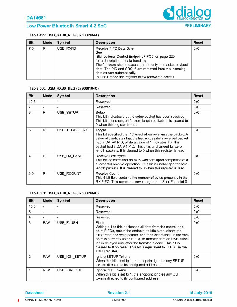
Datasheet Revision 2.1 15-July-2016
CFR0011-120-00-FM Rev 5 342 of 460 © 2016 Dialog Semiconductor
DA14681
Low Power Bluetooth Smart 4.2 SoC PRELIMINARY
7:0 R USB_RXFD Receive FIFO Data ByteSee Bidirectional Control Endpoint FIFO0 on page 220for a description of data handling.The firmware should expect to read only the packet payload data. The PID and CRC16 are removed from the incoming data stream automatically.In TEST mode this register allow read/write access.
0x0
Table 499: USB_RXD0_REG (0x5000184A)
Bit Mode Symbol Description Reset
Table 500: USB_RXS0_REG (0x5000184C)
Bit Mode Symbol Description Reset
15:8 - - Reserved 0x0
7 - - Reserved 0x0
6 R USB_SETUP SetupThis bit indicates that the setup packet has been received. This bit is unchanged for zero length packets. It is cleared to 0 when this register is read.
0x0
5 R USB_TOGGLE_RX0 ToggleThis bit specified the PID used when receiving the packet. A value of 0 indicates that the last successfully received packet had a DATA0 PID, while a value of 1 indicates that this packet had a DATA1 PID. This bit is unchanged for zero length packets. It is cleared to 0 when this register is read.
0x0
4 R USB_RX_LAST Receive Last BytesThis bit indicates that an ACK was sent upon completion of a successful receive operation. This bit is unchanged for zero length packets. It is cleared to 0 when this register is read.
0x0
3:0 R USB_RCOUNT Receive CountThis 4-bit field contains the number of bytes presently in the RX FIFO. This number is never larger than 8 for Endpoint 0.
0x0
Table 501: USB_RXC0_REG (0x5000184E)
Bit Mode Symbol Description Reset
15:6 - - Reserved 0x0
5 - - Reserved 0x0
4 - - Reserved 0x0
3 R/W USB_FLUSH FlushWriting a 1 to this bit flushes all data from the control end-point FIFOs, resets the endpoint to Idle state, clears the FIFO read and write pointer, and then clears itself. If the end-point is currently using FIFO0 to transfer data on USB, flush-ing is delayed until after the transfer is done. This bit is cleared to 0 on reset. This bit is equivalent to FLUSH in the TXC0 register.
0x0
2 R/W USB_IGN_SETUP Ignore SETUP TokensWhen this bit is set to 1, the endpoint ignores any SETUP tokens directed to its configured address.
0x0
1 R/W USB_IGN_OUT Ignore OUT TokensWhen this bit is set to 1, the endpoint ignores any OUT tokens directed to its configured address.
0x0

Datasheet Revision 2.1 15-July-2016
CFR0011-120-00-FM Rev 5 343 of 460 © 2016 Dialog Semiconductor
DA14681
Low Power Bluetooth Smart 4.2 SoC PRELIMINARY
0 R/W USB_RX_EN Receive EnableOUT packet reception is disabled after every data packet is received, or when a STALL handshake is returned in response to an OUT token. A 1 must be written to this bit to re-enable data reception. Reception of SETUP packets is always enabled. In the case of back-to-back SETUP packets (for a given endpoint) where a valid SETUP packet is received with no other intervening non-SETUP tokens, the Endpoint Controller discards the new SETUP packet and returns an ACK handshake. If any other reasons prevent the Endpoint Controller from accepting the SETUP packet, it must not generate a handshake. This allows recovery from a condition where the ACK of the first SETUP token was lost by the host.
0x0
Table 501: USB_RXC0_REG (0x5000184E)
Bit Mode Symbol Description Reset
Table 502: USB_EPC1_REG (0x50001850)
Bit Mode Symbol Description Reset
15:8 - - Reserved 0x0
7 R/W USB_STALL StallSetting this bit to 1 causes the chip to generate STALL hand-shakes under the following conditions:The transmit FIFO is enabled and an IN token is received.The receive FIFO is enabled and an OUT token is received.Setting this bit to 1 does not generate a STALL handshake in response to a SETUP token
0x0
6 - - Reserved 0x0
5 R/W USB_ISO IsochronousWhen this bit is set to 1, the endpoint is isochronous. This implies that no NAK is sent if the endpoint is not ready but enabled; i.e. If an IN token is received and no data is availa-ble in the FIFO to transmit, or if an OUT token is received and the FIFO is full since there is no USB handshake for isochronous transfers.
0x0
4 R/W USB_EP_EN Endpoint EnableWhen this bit is set to 1, the EP[3:0] field is used in address comparison, together with the AD[6:0] field in the FAR regis-ter. See Section36.8for a description. When cleared to 0, the endpoint does not respond to any token on the USB bus.
0x0
3:0 R/W USB_EP Endpoint AddressThis 4-bit field holds the endpoint address.
0x0
Table 503: USB_TXD1_REG (0x50001852)
Bit Mode Symbol Description Reset
15:8 - - Reserved 0x0

Datasheet Revision 2.1 15-July-2016
CFR0011-120-00-FM Rev 5 344 of 460 © 2016 Dialog Semiconductor
DA14681
Low Power Bluetooth Smart 4.2 SoC PRELIMINARY
7:0 W USB_TXFD Transmit FIFO Data ByteSee Transmit Endpoint FIFOs on page 222for a description of endpoint FIFO data handling. The firm-ware is expected to write only the packet payload data. PID and CRC16 are inserted automatically in the transmit data stream.In TEST mode this register allow read/write access via the core bus.
0x0
Table 503: USB_TXD1_REG (0x50001852)
Bit Mode Symbol Description Reset
Table 504: USB_TXS1_REG (0x50001854)
Bit Mode Symbol Description Reset
15:8 - - Reserved 0x0
7 R USB_TX_URUN Transmit FIFO UnderrunThis bit is set to 1, if the transmit FIFO becomes empty dur-ing a transmission, and no new data is written to the FIFO. If so, the Media Access Controller (MAC) forces a bit stuff error followed by an EOP. This bit is cleared to 0, when this regis-ter is read.
0x0
6 R USB_ACK_STAT Acknowledge StatusThis bit is interpreted when TX_DONE is set. It's function dif-fers depending on whether ISO (ISO in the EPCx register is set) or non-ISO operation (ISO is reset) is used.For non-ISO operation, this bit indicates the acknowledge status (from the host) about the ACK for the previously sent packet. This bit itself is set to 1, when an ACK is received; otherwise, it is cleared to 0.For ISO operation, this bit is set if a frame number LSB match (see IGN_ISOMSK bit in the USB_TXCx_REG) occurs, and data was sent in response to an IN token. Other-wise, this bit is cleared to 0, the FIFO is flushed and TX_DONE is set.This bit is also cleared to 0, when this register is read.
0x0
5 R USB_TX_DONE Transmission DoneWhen set to 1, this bit indicates that the endpoint responded to a USB packet. Three conditions can cause this bit to be set:A data packet completed transmission in response to an IN token with non-ISO operation.The endpoint sent a STALL handshake in response to an IN tokenA scheduled ISO frame was transmitted or discarded.This bit is cleared to 0 when this register is read.
0x0
4:0 R USB_TCOUNT Transmission CountThis 5-bit field holds the number of empty bytes available in the FIFO. If this number is greater than 31, a value of 31 is actually reported.
0x1F
Table 505: USB_TXC1_REG (0x50001856)
Bit Mode Symbol Description Reset
15:8 - - Reserved 0x0

Datasheet Revision 2.1 15-July-2016
CFR0011-120-00-FM Rev 5 345 of 460 © 2016 Dialog Semiconductor
DA14681
Low Power Bluetooth Smart 4.2 SoC PRELIMINARY
7 R/W USB_IGN_ISOMSK Ignore ISO MaskThis bit has an effect only if the endpoint is set to be isochro-nous. If set to 1, this bit disables locking of specific frame numbers with the alternate function of the TOGGLE bit. Thus data is transmitted upon reception of the next IN token. If cleared to 0, data is only transmitted when FNL0 matches TOGGLE. This bit is cleared to 0 after reset.
0x0
6:5 R/W USB_TFWL Transmit FIFO Warning LimitThese bits specify how many more bytes can be transmitted from the respective FIFO before an underrun condition occurs. If the number of bytes remaining in the FIFO is equal to or less than the selected warning limit, the TXWARN bit in the FWEV register is set. To avoid interrupts caused by set-ting this bit while the FIFO is being filled before a transmis-sion begins, TXWARN is only set when transmission from the endpoint is enabled (TX_ENn in the TXCn register is set).TFWL[1:0] :00: TFWL disabled01: Less than 5 bytes remaining in FIFO10: Less than 9 bytes remaining in FIFO11: Less than 17 bytes remaining in FIFO
0x0
4 R/W USB_RFF Refill FIFOSetting the LAST bit to 1 automatically saves the Transmit Read Pointer (TXRP) to a buffer. When the RFF bit is set to 1, the buffered TXRP is reloaded into the TXRP. This allows the user to repeat the last transaction if no ACK was received from the host. If the MAC is currently using the FIFO to transmit, TXRP is reloaded only after the transmis-sion is complete. After reload, this bit is cleared to 0 by hard-ware.
0x0
3 R/W USB_FLUSH Flush FIFOWriting a 1 to this bit flushes all data from the corresponding transmit FIFO, resets the endpoint to Idle state, and clears both the FIFO read and write pointers. If the MAC is currently using the FIFO to transmit, data is flushed after the transmis-sion is complete. After data flushing, this bit is cleared to 0 by hardware.
0x0
2 R/W USB_TOGGLE_TX ToggleThe function of this bit differs depending on whether ISO (ISO bit in the EPCn register is set to 1) or non-ISO opera-tion (ISO bit is cleared to 0) is used.For non-ISO operation, it specifies the PID used when trans-mitting the packet. A value of 0 causes a DATA0 PID to be generated, while a value of 1 causes a DATA1 PID to be generated.For ISO operation, this bit and the LSB of the frame counter (FNL0) act as a mask for the TX_EN bit to allow pre-queuing of packets to specific frame numbers; I.e. transmission is enabled only if bit 0 in the FNL register is set to TOGGLE. If an IN token is not received while this condition is true, the contents of the FIFO are flushed with the next SOF. If the endpoint is set to ISO, data is always transferred with a DATA0 PID.
0x0
Table 505: USB_TXC1_REG (0x50001856)
Bit Mode Symbol Description Reset

Datasheet Revision 2.1 15-July-2016
CFR0011-120-00-FM Rev 5 346 of 460 © 2016 Dialog Semiconductor
DA14681
Low Power Bluetooth Smart 4.2 SoC PRELIMINARY
1 R/W USB_LAST Last ByteSetting this bit to 1 indicates that the entire packet has been written into the FIFO. This is used especially for streaming data to the FIFO while the actual transmission occurs. If the LAST bit is not set to 1 and the transmit FIFO becomes empty during a transmission, a stuff error followed by an EOP is forced on the bus. Zero length packets are indicated by setting this bit without writing any data to the FIFO.The transmit state machine transmits the payload data, CRC16 and the EOP signal before clearing this bit.
0x0
0 R/W USB_TX_EN Transmission EnableThis bit enables data transmission from the FIFO. It is cleared to 0 by hardware after transmitting a single packet or after a STALL handshake in response to an IN token. It must be set to 1 by firmware to start packet transmission.
0x0
Table 505: USB_TXC1_REG (0x50001856)
Bit Mode Symbol Description Reset
Table 506: USB_EPC2_REG (0x50001858)
Bit Mode Symbol Description Reset
15:8 - - Reserved 0x0
7 R/W USB_STALL StallSetting this bit to 1 causes the chip to generate STALL hand-shakes under the following conditions:The transmit FIFO is enabled and an IN token is received.The receive FIFO is enabled and an OUT token is received.Setting this bit to 1 does not generate a STALL handshake in response to a SETUP token
0x0
6 - - Reserved 0x0
5 R/W USB_ISO IsochronousWhen this bit is set to 1, the endpoint is isochronous. This implies that no NAK is sent if the endpoint is not ready but enabled; i.e. If an IN token is received and no data is availa-ble in the FIFO to transmit, or if an OUT token is received and the FIFO is full since there is no USB handshake for isochronous transfers.
0x0
4 R/W USB_EP_EN Endpoint EnableWhen this bit is set to 1, the EP[3:0] field is used in address comparison, together with the AD[6:0] field in the FAR regis-ter. See Section36.8for a description. When cleared to 0, the endpoint does not respond to any token on the USB bus.
0x0
3:0 R/W USB_EP Endpoint AddressThis 4-bit field holds the endpoint address.
0x0
Table 507: USB_RXD1_REG (0x5000185A)
Bit Mode Symbol Description Reset
15:8 - - Reserved 0x0

Datasheet Revision 2.1 15-July-2016
CFR0011-120-00-FM Rev 5 347 of 460 © 2016 Dialog Semiconductor
DA14681
Low Power Bluetooth Smart 4.2 SoC PRELIMINARY
7:0 R USB_RXFD Receive FIFO Data ByteSee Receive Endpoint FIFO on page 223for a description of Endpoint FIFO data handling.The firm-ware should expect to read only the packet payload data. The PID and CRC16 are terminated by the receive state machine.In TEST mode this register allow read/write access via the core bus.
0x0
Table 507: USB_RXD1_REG (0x5000185A)
Bit Mode Symbol Description Reset
Table 508: USB_RXS1_REG (0x5000185C)
Bit Mode Symbol Description Reset
15:8 - - Reserved 0x0
7 R USB_RX_ERR Receive ErrorWhen set to 1, this bit indicates a media error, such as bit-stuffing or CRC. If this bit is set to 1, the firmware must flush the respective FIFO.
0x0
6 R USB_SETUP SetupThis bit indicates that the setup packet has been received. It is cleared when this register is read.
0x0
5 R USB_TOGGLE_RX ToggleThe function of this bit differs depending on whether ISO (ISO in the EPCn register is set) or non-ISO operation (ISO is reset) is used.For non-ISO operation, a value of 0 indicates that the last successfully received packet had a DATA0 PID, while a value of 1 indicates that this packet had a DATA1 PID.For ISO operation, this bit reflects the LSB of the frame num-ber (FNL0) after a packet was successfully received for this endpoint.This bit is reset to 0 by reading the RXSn register.
0x0
4 R USB_RX_LAST Receive LastThis bit indicates that an ACK was sent upon completion of a successful receive operation. This bit is cleared to 0 when this register is read.
0x0
3:0 R USB_RCOUNT Receive CounterThis 4-bit field contains the number of bytes presently in the endpoint receive FIFO. If this number is greater than 15, a value of 15 is actually reported.
0x0
Table 509: USB_RXC1_REG (0x5000185E)
Bit Mode Symbol Description Reset
15:7 - - Reserved 0x0
6:5 R/W USB_RFWL Receive FIFO Warning LimitThese bits specify how many more bytes can be received to the respective FIFO before an overrun condition occurs. If the number of empty bytes remaining in the FIFO is equal to or less than the selected warning limit, the RXWARN bit in the FWEV register is set to 1.RFWL[1:0] :00: RFWL disabled01: Less than 5 bytes remaining in FIFO10: Less than 9 bytes remaining in FIFO11: Less than 17 bytes remaining in FIFO
0x0

Datasheet Revision 2.1 15-July-2016
CFR0011-120-00-FM Rev 5 348 of 460 © 2016 Dialog Semiconductor
DA14681
Low Power Bluetooth Smart 4.2 SoC PRELIMINARY
4 - - Reserved 0x0
3 R/W USB_FLUSH Flush FIFOWriting a 1 to this bit flushes all data from the corresponding receive FIFO, resets the endpoint to Idle state, and resets both the FIFO read and write pointers. If the MAC is currently using the FIFO to receive data, flushing is delayed until after receiving is completed.
0x0
2 R/W USB_IGN_SETUP Ignore SETUP TokensWhen this bit is set to 1, the endpoint ignores any SETUP tokens directed to its configured address.
0x0
1 - - Reserved 0x0
0 R/W USB_RX_EN Receive EnableOUT packet cannot be received after every data packet is received, or when a STALL handshake is returned in response to an OUT token. This bit must be written with a 1 to re-enable data reception. SETUP packets can always be received. In the case of back-to-back SETUP packets (for a given endpoint) where a valid SETUP packet has been received with no other intervening non-SETUP tokens, the receive state machine discards the new SETUP packet and returns an ACK handshake. If, for any other reason, the receive state machine cannot accept the SETUP packet, no HANDSHAKE should be generated.
0x0
Table 509: USB_RXC1_REG (0x5000185E)
Bit Mode Symbol Description Reset
Table 510: USB_EPC3_REG (0x50001860)
Bit Mode Symbol Description Reset
15:8 - - Reserved 0x0
7 R/W USB_STALL StallSetting this bit to 1 causes the chip to generate STALL hand-shakes under the following conditions:The transmit FIFO is enabled and an IN token is received.The receive FIFO is enabled and an OUT token is received.Setting this bit to 1 does not generate a STALL handshake in response to a SETUP token
0x0
6 - - Reserved 0x0
5 R/W USB_ISO IsochronousWhen this bit is set to 1, the endpoint is isochronous. This implies that no NAK is sent if the endpoint is not ready but enabled; i.e. If an IN token is received and no data is availa-ble in the FIFO to transmit, or if an OUT token is received and the FIFO is full since there is no USB handshake for isochronous transfers.
0x0
4 R/W USB_EP_EN Endpoint EnableWhen this bit is set to 1, the EP[3:0] field is used in address comparison, together with the AD[6:0] field in the FAR regis-ter. See Section36.8for a description. When cleared to 0, the endpoint does not respond to any token on the USB bus.
0x0
3:0 R/W USB_EP Endpoint AddressThis 4-bit field holds the endpoint address.
0x0

Datasheet Revision 2.1 15-July-2016
CFR0011-120-00-FM Rev 5 349 of 460 © 2016 Dialog Semiconductor
DA14681
Low Power Bluetooth Smart 4.2 SoC PRELIMINARY
Table 511: USB_TXD2_REG (0x50001862)
Bit Mode Symbol Description Reset
15:8 - - Reserved 0x0
7:0 W USB_TXFD Transmit FIFO Data ByteSee Transmit Endpoint FIFOs on page 222for a description of endpoint FIFO data handling. The firm-ware is expected to write only the packet payload data. PID and CRC16 are inserted automatically in the transmit data stream.In TEST mode this register allow read/write access via the core bus.
0x0
Table 512: USB_TXS2_REG (0x50001864)
Bit Mode Symbol Description Reset
15:8 - - Reserved 0x0
7 R USB_TX_URUN Transmit FIFO UnderrunThis bit is set to 1, if the transmit FIFO becomes empty dur-ing a transmission, and no new data is written to the FIFO. If so, the Media Access Controller (MAC) forces a bit stuff error followed by an EOP. This bit is cleared to 0, when this regis-ter is read.
0x0
6 R USB_ACK_STAT Acknowledge StatusThis bit is interpreted when TX_DONE is set. It's function dif-fers depending on whether ISO (ISO in the EPCx register is set) or non-ISO operation (ISO is reset) is used.For non-ISO operation, this bit indicates the acknowledge status (from the host) about the ACK for the previously sent packet. This bit itself is set to 1, when an ACK is received; otherwise, it is cleared to 0.For ISO operation, this bit is set if a frame number LSB match (see IGN_ISOMSK bit in the USB_TXCx_REG) occurs, and data was sent in response to an IN token. Other-wise, this bit is cleared to 0, the FIFO is flushed and TX_DONE is set.This bit is also cleared to 0, when this register is read.
0x0
5 R USB_TX_DONE Transmission DoneWhen set to 1, this bit indicates that the endpoint responded to a USB packet. Three conditions can cause this bit to be set:A data packet completed transmission in response to an IN token with non-ISO operation.The endpoint sent a STALL handshake in response to an IN tokenA scheduled ISO frame was transmitted or discarded.This bit is cleared to 0 when this register is read.
0x0
4:0 R USB_TCOUNT Transmission CountThis 5-bit field holds the number of empty bytes available in the FIFO. If this number is greater than 31, a value of 31 is actually reported.
0x1F
Table 513: USB_TXC2_REG (0x50001866)
Bit Mode Symbol Description Reset
15:8 - - Reserved 0x0

Datasheet Revision 2.1 15-July-2016
CFR0011-120-00-FM Rev 5 350 of 460 © 2016 Dialog Semiconductor
DA14681
Low Power Bluetooth Smart 4.2 SoC PRELIMINARY
7 R/W USB_IGN_ISOMSK Ignore ISO MaskThis bit has an effect only if the endpoint is set to be isochro-nous. If set to 1, this bit disables locking of specific frame numbers with the alternate function of the TOGGLE bit. Thus data is transmitted upon reception of the next IN token. If cleared to 0, data is only transmitted when FNL0 matches TOGGLE. This bit is cleared to 0 after reset.
0x0
6:5 R/W USB_TFWL Transmit FIFO Warning LimitThese bits specify how many more bytes can be transmitted from the respective FIFO before an underrun condition occurs. If the number of bytes remaining in the FIFO is equal to or less than the selected warning limit, the TXWARN bit in the FWEV register is set. To avoid interrupts caused by set-ting this bit while the FIFO is being filled before a transmis-sion begins, TXWARN is only set when transmission from the endpoint is enabled (TX_ENn in the TXCn register is set).TFWL[1:0] :00: TFWL disabled01: Less than 5 bytes remaining in FIFO10: Less than 9 bytes remaining in FIFO11: Less than 17 bytes remaining in FIFO
0x0
4 R/W USB_RFF Refill FIFOSetting the LAST bit to 1 automatically saves the Transmit Read Pointer (TXRP) to a buffer. When the RFF bit is set to 1, the buffered TXRP is reloaded into the TXRP. This allows the user to repeat the last transaction if no ACK was received from the host. If the MAC is currently using the FIFO to transmit, TXRP is reloaded only after the transmis-sion is complete. After reload, this bit is cleared to 0 by hard-ware.
0x0
3 R/W USB_FLUSH Flush FIFOWriting a 1 to this bit flushes all data from the corresponding transmit FIFO, resets the endpoint to Idle state, and clears both the FIFO read and write pointers. If the MAC is currently using the FIFO to transmit, data is flushed after the transmis-sion is complete. After data flushing, this bit is cleared to 0 by hardware.
0x0
2 R/W USB_TOGGLE_TX ToggleThe function of this bit differs depending on whether ISO (ISO bit in the EPCn register is set to 1) or non-ISO opera-tion (ISO bit is cleared to 0) is used.For non-ISO operation, it specifies the PID used when trans-mitting the packet. A value of 0 causes a DATA0 PID to be generated, while a value of 1 causes a DATA1 PID to be generated.For ISO operation, this bit and the LSB of the frame counter (FNL0) act as a mask for the TX_EN bit to allow pre-queuing of packets to specific frame numbers; I.e. transmission is enabled only if bit 0 in the FNL register is set to TOGGLE. If an IN token is not received while this condition is true, the contents of the FIFO are flushed with the next SOF. If the endpoint is set to ISO, data is always transferred with a DATA0 PID.
0x0
Table 513: USB_TXC2_REG (0x50001866)
Bit Mode Symbol Description Reset

Datasheet Revision 2.1 15-July-2016
CFR0011-120-00-FM Rev 5 351 of 460 © 2016 Dialog Semiconductor
DA14681
Low Power Bluetooth Smart 4.2 SoC PRELIMINARY
1 R/W USB_LAST Last ByteSetting this bit to 1 indicates that the entire packet has been written into the FIFO. This is used especially for streaming data to the FIFO while the actual transmission occurs. If the LAST bit is not set to 1 and the transmit FIFO becomes empty during a transmission, a stuff error followed by an EOP is forced on the bus. Zero length packets are indicated by setting this bit without writing any data to the FIFO.The transmit state machine transmits the payload data, CRC16 and the EOP signal before clearing this bit.
0x0
0 R/W USB_TX_EN Transmission EnableThis bit enables data transmission from the FIFO. It is cleared to 0 by hardware after transmitting a single packet or after a STALL handshake in response to an IN token. It must be set to 1 by firmware to start packet transmission.
0x0
Table 513: USB_TXC2_REG (0x50001866)
Bit Mode Symbol Description Reset
Table 514: USB_EPC4_REG (0x50001868)
Bit Mode Symbol Description Reset
15:8 - - Reserved 0x0
7 R/W USB_STALL StallSetting this bit to 1 causes the chip to generate STALL hand-shakes under the following conditions:The transmit FIFO is enabled and an IN token is received.The receive FIFO is enabled and an OUT token is received.Setting this bit to 1 does not generate a STALL handshake in response to a SETUP token
0x0
6 - - Reserved 0x0
5 R/W USB_ISO IsochronousWhen this bit is set to 1, the endpoint is isochronous. This implies that no NAK is sent if the endpoint is not ready but enabled; i.e. If an IN token is received and no data is availa-ble in the FIFO to transmit, or if an OUT token is received and the FIFO is full since there is no USB handshake for isochronous transfers.
0x0
4 R/W USB_EP_EN Endpoint EnableWhen this bit is set to 1, the EP[3:0] field is used in address comparison, together with the AD[6:0] field in the FAR regis-ter. See Section36.8for a description. When cleared to 0, the endpoint does not respond to any token on the USB bus.
0x0
3:0 R/W USB_EP Endpoint AddressThis 4-bit field holds the endpoint address.
0x0
Table 515: USB_RXD2_REG (0x5000186A)
Bit Mode Symbol Description Reset
15:8 - - Reserved 0x0

Datasheet Revision 2.1 15-July-2016
CFR0011-120-00-FM Rev 5 352 of 460 © 2016 Dialog Semiconductor
DA14681
Low Power Bluetooth Smart 4.2 SoC PRELIMINARY
7:0 R USB_RXFD Receive FIFO Data ByteSee Receive Endpoint FIFO on page 223for a description of Endpoint FIFO data handling.The firm-ware should expect to read only the packet payload data. The PID and CRC16 are terminated by the receive state machine.In TEST mode this register allow read/write access via the core bus.
0x0
Table 515: USB_RXD2_REG (0x5000186A)
Bit Mode Symbol Description Reset
Table 516: USB_RXS2_REG (0x5000186C)
Bit Mode Symbol Description Reset
15:8 - - Reserved 0x0
7 R USB_RX_ERR Receive ErrorWhen set to 1, this bit indicates a media error, such as bit-stuffing or CRC. If this bit is set to 1, the firmware must flush the respective FIFO.
0x0
6 R USB_SETUP SetupThis bit indicates that the setup packet has been received. It is cleared when this register is read.
0x0
5 R USB_TOGGLE_RX ToggleThe function of this bit differs depending on whether ISO (ISO in the EPCn register is set) or non-ISO operation (ISO is reset) is used.For non-ISO operation, a value of 0 indicates that the last successfully received packet had a DATA0 PID, while a value of 1 indicates that this packet had a DATA1 PID.For ISO operation, this bit reflects the LSB of the frame num-ber (FNL0) after a packet was successfully received for this endpoint.This bit is reset to 0 by reading the RXSn register.
0x0
4 R USB_RX_LAST Receive LastThis bit indicates that an ACK was sent upon completion of a successful receive operation. This bit is cleared to 0 when this register is read.
0x0
3:0 R USB_RCOUNT Receive CounterThis 4-bit field contains the number of bytes presently in the endpoint receive FIFO. If this number is greater than 15, a value of 15 is actually reported.
0x0
Table 517: USB_RXC2_REG (0x5000186E)
Bit Mode Symbol Description Reset
15:7 - - Reserved 0x0
6:5 R/W USB_RFWL Receive FIFO Warning LimitThese bits specify how many more bytes can be received to the respective FIFO before an overrun condition occurs. If the number of empty bytes remaining in the FIFO is equal to or less than the selected warning limit, the RXWARN bit in the FWEV register is set to 1.RFWL[1:0] :00: RFWL disabled01: Less than 5 bytes remaining in FIFO10: Less than 9 bytes remaining in FIFO11: Less than 17 bytes remaining in FIFO
0x0

Datasheet Revision 2.1 15-July-2016
CFR0011-120-00-FM Rev 5 353 of 460 © 2016 Dialog Semiconductor
DA14681
Low Power Bluetooth Smart 4.2 SoC PRELIMINARY
4 - - Reserved 0x0
3 R/W USB_FLUSH Flush FIFOWriting a 1 to this bit flushes all data from the corresponding receive FIFO, resets the endpoint to Idle state, and resets both the FIFO read and write pointers. If the MAC is currently using the FIFO to receive data, flushing is delayed until after receiving is completed.
0x0
2 R/W USB_IGN_SETUP Ignore SETUP TokensWhen this bit is set to 1, the endpoint ignores any SETUP tokens directed to its configured address.
0x0
1 - - Reserved 0x0
0 R/W USB_RX_EN Receive EnableOUT packet cannot be received after every data packet is received, or when a STALL handshake is returned in response to an OUT token. This bit must be written with a 1 to re-enable data reception. SETUP packets can always be received. In the case of back-to-back SETUP packets (for a given endpoint) where a valid SETUP packet has been received with no other intervening non-SETUP tokens, the receive state machine discards the new SETUP packet and returns an ACK handshake. If, for any other reason, the receive state machine cannot accept the SETUP packet, no HANDSHAKE should be generated.
0x0
Table 517: USB_RXC2_REG (0x5000186E)
Bit Mode Symbol Description Reset
Table 518: USB_EPC5_REG (0x50001870)
Bit Mode Symbol Description Reset
15:8 - - Reserved 0x0
7 R/W USB_STALL StallSetting this bit to 1 causes the chip to generate STALL hand-shakes under the following conditions:The transmit FIFO is enabled and an IN token is received.The receive FIFO is enabled and an OUT token is received.Setting this bit to 1 does not generate a STALL handshake in response to a SETUP token
0x0
6 - - Reserved 0x0
5 R/W USB_ISO IsochronousWhen this bit is set to 1, the endpoint is isochronous. This implies that no NAK is sent if the endpoint is not ready but enabled; i.e. If an IN token is received and no data is availa-ble in the FIFO to transmit, or if an OUT token is received and the FIFO is full since there is no USB handshake for isochronous transfers.
0x0
4 R/W USB_EP_EN Endpoint EnableWhen this bit is set to 1, the EP[3:0] field is used in address comparison, together with the AD[6:0] field in the FAR regis-ter. See Section36.8for a description. When cleared to 0, the endpoint does not respond to any token on the USB bus.
0x0
3:0 R/W USB_EP Endpoint AddressThis 4-bit field holds the endpoint address.
0x0
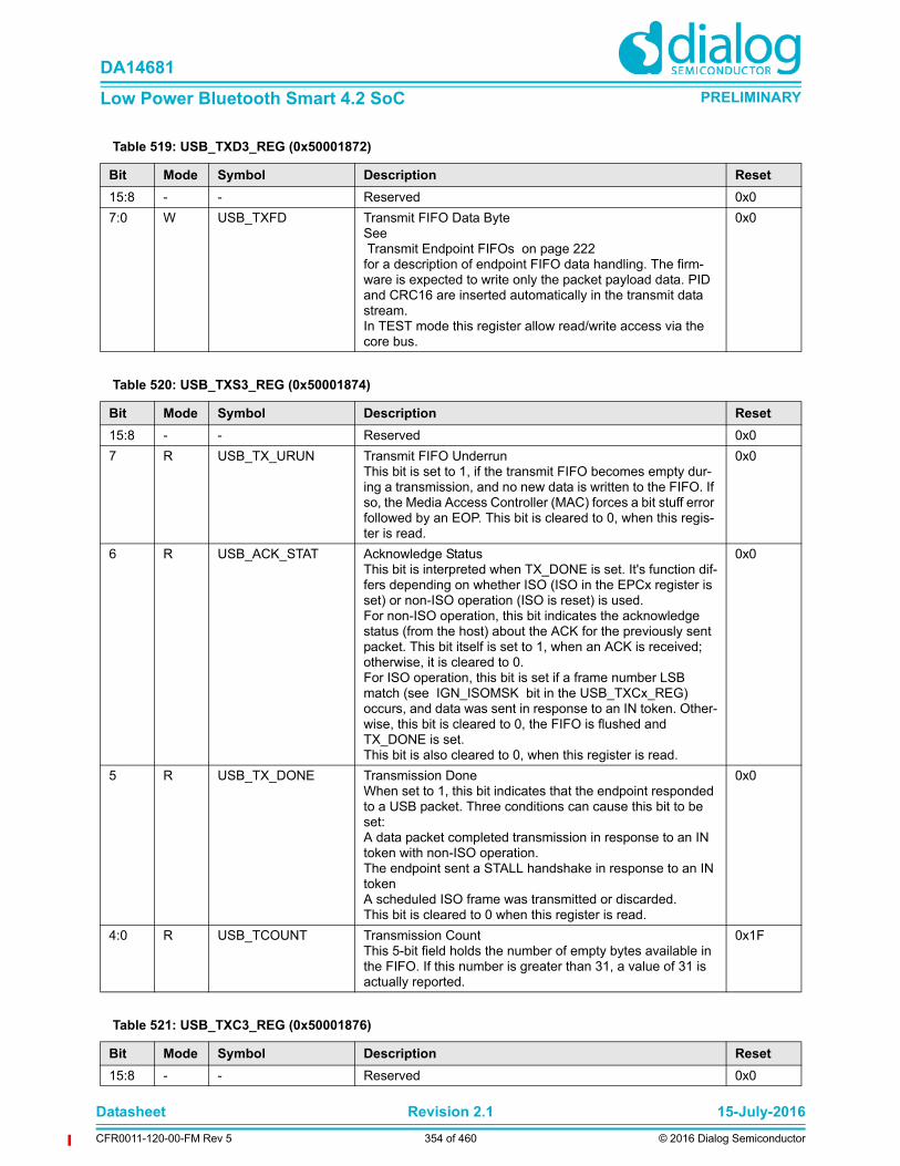
Datasheet Revision 2.1 15-July-2016
CFR0011-120-00-FM Rev 5 354 of 460 © 2016 Dialog Semiconductor
DA14681
Low Power Bluetooth Smart 4.2 SoC PRELIMINARY
Table 519: USB_TXD3_REG (0x50001872)
Bit Mode Symbol Description Reset
15:8 - - Reserved 0x0
7:0 W USB_TXFD Transmit FIFO Data ByteSee Transmit Endpoint FIFOs on page 222for a description of endpoint FIFO data handling. The firm-ware is expected to write only the packet payload data. PID and CRC16 are inserted automatically in the transmit data stream.In TEST mode this register allow read/write access via the core bus.
0x0
Table 520: USB_TXS3_REG (0x50001874)
Bit Mode Symbol Description Reset
15:8 - - Reserved 0x0
7 R USB_TX_URUN Transmit FIFO UnderrunThis bit is set to 1, if the transmit FIFO becomes empty dur-ing a transmission, and no new data is written to the FIFO. If so, the Media Access Controller (MAC) forces a bit stuff error followed by an EOP. This bit is cleared to 0, when this regis-ter is read.
0x0
6 R USB_ACK_STAT Acknowledge StatusThis bit is interpreted when TX_DONE is set. It's function dif-fers depending on whether ISO (ISO in the EPCx register is set) or non-ISO operation (ISO is reset) is used.For non-ISO operation, this bit indicates the acknowledge status (from the host) about the ACK for the previously sent packet. This bit itself is set to 1, when an ACK is received; otherwise, it is cleared to 0.For ISO operation, this bit is set if a frame number LSB match (see IGN_ISOMSK bit in the USB_TXCx_REG) occurs, and data was sent in response to an IN token. Other-wise, this bit is cleared to 0, the FIFO is flushed and TX_DONE is set.This bit is also cleared to 0, when this register is read.
0x0
5 R USB_TX_DONE Transmission DoneWhen set to 1, this bit indicates that the endpoint responded to a USB packet. Three conditions can cause this bit to be set:A data packet completed transmission in response to an IN token with non-ISO operation.The endpoint sent a STALL handshake in response to an IN tokenA scheduled ISO frame was transmitted or discarded.This bit is cleared to 0 when this register is read.
0x0
4:0 R USB_TCOUNT Transmission CountThis 5-bit field holds the number of empty bytes available in the FIFO. If this number is greater than 31, a value of 31 is actually reported.
0x1F
Table 521: USB_TXC3_REG (0x50001876)
Bit Mode Symbol Description Reset
15:8 - - Reserved 0x0

Datasheet Revision 2.1 15-July-2016
CFR0011-120-00-FM Rev 5 355 of 460 © 2016 Dialog Semiconductor
DA14681
Low Power Bluetooth Smart 4.2 SoC PRELIMINARY
7 R/W USB_IGN_ISOMSK Ignore ISO MaskThis bit has an effect only if the endpoint is set to be isochro-nous. If set to 1, this bit disables locking of specific frame numbers with the alternate function of the TOGGLE bit. Thus data is transmitted upon reception of the next IN token. If cleared to 0, data is only transmitted when FNL0 matches TOGGLE. This bit is cleared to 0 after reset.
0x0
6:5 R/W USB_TFWL Transmit FIFO Warning LimitThese bits specify how many more bytes can be transmitted from the respective FIFO before an underrun condition occurs. If the number of bytes remaining in the FIFO is equal to or less than the selected warning limit, the TXWARN bit in the FWEV register is set. To avoid interrupts caused by set-ting this bit while the FIFO is being filled before a transmis-sion begins, TXWARN is only set when transmission from the endpoint is enabled (TX_ENn in the TXCn register is set).TFWL[1:0] :00: TFWL disabled01: Less than 5 bytes remaining in FIFO10: Less than 9 bytes remaining in FIFO11: Less than 17 bytes remaining in FIFO
0x0
4 R/W USB_RFF Refill FIFOSetting the LAST bit to 1 automatically saves the Transmit Read Pointer (TXRP) to a buffer. When the RFF bit is set to 1, the buffered TXRP is reloaded into the TXRP. This allows the user to repeat the last transaction if no ACK was received from the host. If the MAC is currently using the FIFO to transmit, TXRP is reloaded only after the transmis-sion is complete. After reload, this bit is cleared to 0 by hard-ware.
0x0
3 R/W USB_FLUSH Flush FIFOWriting a 1 to this bit flushes all data from the corresponding transmit FIFO, resets the endpoint to Idle state, and clears both the FIFO read and write pointers. If the MAC is currently using the FIFO to transmit, data is flushed after the transmis-sion is complete. After data flushing, this bit is cleared to 0 by hardware.
0x0
2 R/W USB_TOGGLE_TX ToggleThe function of this bit differs depending on whether ISO (ISO bit in the EPCn register is set to 1) or non-ISO opera-tion (ISO bit is cleared to 0) is used.For non-ISO operation, it specifies the PID used when trans-mitting the packet. A value of 0 causes a DATA0 PID to be generated, while a value of 1 causes a DATA1 PID to be generated.For ISO operation, this bit and the LSB of the frame counter (FNL0) act as a mask for the TX_EN bit to allow pre-queuing of packets to specific frame numbers; I.e. transmission is enabled only if bit 0 in the FNL register is set to TOGGLE. If an IN token is not received while this condition is true, the contents of the FIFO are flushed with the next SOF. If the endpoint is set to ISO, data is always transferred with a DATA0 PID.
0x0
Table 521: USB_TXC3_REG (0x50001876)
Bit Mode Symbol Description Reset

Datasheet Revision 2.1 15-July-2016
CFR0011-120-00-FM Rev 5 356 of 460 © 2016 Dialog Semiconductor
DA14681
Low Power Bluetooth Smart 4.2 SoC PRELIMINARY
1 R/W USB_LAST Last ByteSetting this bit to 1 indicates that the entire packet has been written into the FIFO. This is used especially for streaming data to the FIFO while the actual transmission occurs. If the LAST bit is not set to 1 and the transmit FIFO becomes empty during a transmission, a stuff error followed by an EOP is forced on the bus. Zero length packets are indicated by setting this bit without writing any data to the FIFO.The transmit state machine transmits the payload data, CRC16 and the EOP signal before clearing this bit.
0x0
0 R/W USB_TX_EN Transmission EnableThis bit enables data transmission from the FIFO. It is cleared to 0 by hardware after transmitting a single packet or after a STALL handshake in response to an IN token. It must be set to 1 by firmware to start packet transmission.
0x0
Table 521: USB_TXC3_REG (0x50001876)
Bit Mode Symbol Description Reset
Table 522: USB_EPC6_REG (0x50001878)
Bit Mode Symbol Description Reset
15:8 - - Reserved 0x0
7 R/W USB_STALL StallSetting this bit to 1 causes the chip to generate STALL hand-shakes under the following conditions:The transmit FIFO is enabled and an IN token is received.The receive FIFO is enabled and an OUT token is received.Setting this bit to 1 does not generate a STALL handshake in response to a SETUP token
0x0
6 - - Reserved 0x0
5 R/W USB_ISO IsochronousWhen this bit is set to 1, the endpoint is isochronous. This implies that no NAK is sent if the endpoint is not ready but enabled; i.e. If an IN token is received and no data is availa-ble in the FIFO to transmit, or if an OUT token is received and the FIFO is full since there is no USB handshake for isochronous transfers.
0x0
4 R/W USB_EP_EN Endpoint EnableWhen this bit is set to 1, the EP[3:0] field is used in address comparison, together with the AD[6:0] field in the FAR regis-ter. See Section36.8for a description. When cleared to 0, the endpoint does not respond to any token on the USB bus.
0x0
3:0 R/W USB_EP Endpoint AddressThis 4-bit field holds the endpoint address.
0x0
Table 523: USB_RXD3_REG (0x5000187A)
Bit Mode Symbol Description Reset
15:8 - - Reserved 0x0

Datasheet Revision 2.1 15-July-2016
CFR0011-120-00-FM Rev 5 357 of 460 © 2016 Dialog Semiconductor
DA14681
Low Power Bluetooth Smart 4.2 SoC PRELIMINARY
7:0 R USB_RXFD Receive FIFO Data ByteSee Receive Endpoint FIFO on page 223for a description of Endpoint FIFO data handling.The firm-ware should expect to read only the packet payload data. The PID and CRC16 are terminated by the receive state machine.In TEST mode this register allow read/write access via the core bus.
0x0
Table 523: USB_RXD3_REG (0x5000187A)
Bit Mode Symbol Description Reset
Table 524: USB_RXS3_REG (0x5000187C)
Bit Mode Symbol Description Reset
15:8 - - Reserved 0x0
7 R USB_RX_ERR Receive ErrorWhen set to 1, this bit indicates a media error, such as bit-stuffing or CRC. If this bit is set to 1, the firmware must flush the respective FIFO.
0x0
6 R USB_SETUP SetupThis bit indicates that the setup packet has been received. It is cleared when this register is read.
0x0
5 R USB_TOGGLE_RX ToggleThe function of this bit differs depending on whether ISO (ISO in the EPCn register is set) or non-ISO operation (ISO is reset) is used.For non-ISO operation, a value of 0 indicates that the last successfully received packet had a DATA0 PID, while a value of 1 indicates that this packet had a DATA1 PID.For ISO operation, this bit reflects the LSB of the frame num-ber (FNL0) after a packet was successfully received for this endpoint.This bit is reset to 0 by reading the RXSn register.
0x0
4 R USB_RX_LAST Receive LastThis bit indicates that an ACK was sent upon completion of a successful receive operation. This bit is cleared to 0 when this register is read.
0x0
3:0 R USB_RCOUNT Receive CounterThis 4-bit field contains the number of bytes presently in the endpoint receive FIFO. If this number is greater than 15, a value of 15 is actually reported.
0x0
Table 525: USB_RXC3_REG (0x5000187E)
Bit Mode Symbol Description Reset
15:7 - - Reserved 0x0
6:5 R/W USB_RFWL Receive FIFO Warning LimitThese bits specify how many more bytes can be received to the respective FIFO before an overrun condition occurs. If the number of empty bytes remaining in the FIFO is equal to or less than the selected warning limit, the RXWARN bit in the FWEV register is set to 1.RFWL[1:0] :00: RFWL disabled01: Less than 5 bytes remaining in FIFO10: Less than 9 bytes remaining in FIFO11: Less than 17 bytes remaining in FIFO
0x0

Datasheet Revision 2.1 15-July-2016
CFR0011-120-00-FM Rev 5 358 of 460 © 2016 Dialog Semiconductor
DA14681
Low Power Bluetooth Smart 4.2 SoC PRELIMINARY
4 - - Reserved 0x0
3 R/W USB_FLUSH Flush FIFOWriting a 1 to this bit flushes all data from the corresponding receive FIFO, resets the endpoint to Idle state, and resets both the FIFO read and write pointers. If the MAC is currently using the FIFO to receive data, flushing is delayed until after receiving is completed.
0x0
2 R/W USB_IGN_SETUP Ignore SETUP TokensWhen this bit is set to 1, the endpoint ignores any SETUP tokens directed to its configured address.
0x0
1 - - Reserved 0x0
0 R/W USB_RX_EN Receive EnableOUT packet cannot be received after every data packet is received, or when a STALL handshake is returned in response to an OUT token. This bit must be written with a 1 to re-enable data reception. SETUP packets can always be received. In the case of back-to-back SETUP packets (for a given endpoint) where a valid SETUP packet has been received with no other intervening non-SETUP tokens, the receive state machine discards the new SETUP packet and returns an ACK handshake. If, for any other reason, the receive state machine cannot accept the SETUP packet, no HANDSHAKE should be generated.
0x0
Table 525: USB_RXC3_REG (0x5000187E)
Bit Mode Symbol Description Reset
Table 526: USB_DMA_CTRL_REG (0x500018D0)
Bit Mode Symbol Description Reset
6 R/W USB_DMA_EN 0 = USB DMA control off. (Normal operation)1 = USB_DMA on. DMA channels 0 and 1 are connected byUSB Endpoint according bits USB_DMA_TX and USB_DMA_RX
0x0
5:3 R/W USB_DMA_TX 000 = DMA channels 1 is connected Tx USB Endpoint 1001 = DMA channels 1 is connected Tx USB Endpoint 3010 = DMA channels 1 is connected Tx USB Endpoint 5100, 1xx = Reserved
0x0
2:0 R/W USB_DMA_RX 000 = DMA channels 0 is connected Rx USB Endpoint 2001 = DMA channels 0 is connected Rx USB Endpoint 4010 = DMA channels 0 is connected Rx USB Endpoint 6100, 1xx = Reserved
0x0
Table 527: USB_CHARGER_CTRL_REG (0x500018D4)
Bit Mode Symbol Description Reset
15:6 - - Reserved 0x0
5 R/W IDM_SINK_ON 0 = Disable1 = Enable the Idm_sink to USBm
0x0
4 R/W IDP_SINK_ON 0 = Disable1 = Enable the Idp_sink to USBp
0x0
3 R/W VDM_SRC_ON 0 = Disable1 = Enable Vdm_src to USBm and USB_DCP_DET status bit.
0x0
2 R/W VDP_SRC_ON 0 = Disable1 = Enable the Vdp_src to USB_CHG_DET status bit.
0x0

Datasheet Revision 2.1 15-July-2016
CFR0011-120-00-FM Rev 5 359 of 460 © 2016 Dialog Semiconductor
DA14681
Low Power Bluetooth Smart 4.2 SoC PRELIMINARY
1 R/W IDP_SRC_ON 0 = Disable1 = Enable the Idp_src and Rdm_dwn.
0x0
0 R/W USB_CHARGE_ON 0 = Disable USB charger detect circuit.1 = Enable USB charger detect circuit.
0x0
Table 527: USB_CHARGER_CTRL_REG (0x500018D4)
Bit Mode Symbol Description Reset
Table 528: USB_CHARGER_STAT_REG (0x500018D6)
Bit Mode Symbol Description Reset
15:6 - - Reserved 0x0
5 R USB_DM_VAL2 0 = USBm <2.3V1 = USBm >2.5V
0x0
4 R USB_DP_VAL2 0: USBp < 2.3V1: USBp > 2.5V
0x0
3 R USB_DM_VAL 0 = USBm < 0.8V1 = USBm > 1.5V (PS2 or Proprietary Charger)
0x0
2 R USB_DP_VAL 0 = USBp < 0.8V1 = USBp > 1.5V
0x0
1 R USB_CHG_DET 0 = Standard downstream or nothing connected.1 = Charging Downstream Port (CDP) or Dedicated Charg-ing.
0x0
0 R USB_DCP_DET 0 = Charging downstream port is detected.1 = Dedicated charger is detected.Control bit VDM_SRC_ON must be set to validate this status bit.Note: This register shows the actual status.
0x0

Datasheet Revision 2.1 15-July-2016
CFR0011-120-00-FM Rev 5 360 of 460 © 2016 Dialog Semiconductor
DA14681
Low Power Bluetooth Smart 4.2 SoC PRELIMINARY
37.16 GPADC REGISTER FILE
Table 529: Register map GPADC
Address Port Description
0x50001900 GP_ADC_CTRL_REG General Purpose ADC Control Register
0x50001902 GP_ADC_CTRL2_REG General Purpose ADC Second Control Register
0x50001904 GP_ADC_CTRL3_REG General Purpose ADC Third Control Register
0x50001906 GP_ADC_OFFP_REG General Purpose ADC Positive Offset Register
0x50001908 GP_ADC_OFFN_REG General Purpose ADC Negative Offset Register
0x5000190A GP_ADC_CLEAR_INT_REG General Purpose ADC Clear Interrupt Register
0x5000190C GP_ADC_RESULT_REG General Purpose ADC Result Register
Table 530: GP_ADC_CTRL_REG (0x50001900)
Bit Mode Symbol Description Reset
15 R/W GP_ADC_LDO_ZERO
1: Samples and disconnects VREF, should be refreshed fre-quently. Note that the LDO consumpes power when bit is set.
0x0
14 R/W GP_ADC_CHOP 0: Chopper mode off1: Chopper mode enabled. Takes two samples with opposite GP_ADC_SIGN to cancel the internal offset voltage of the ADC; Highly recommended for DC-measurements.
0x0
13 R/W GP_ADC_SIGN 0: Default1: Conversion with opposite sign at input and output to can-cel out the internal offset of the ADC and low-frequency
0x0
12:8 R/W GP_ADC_SEL ADC input selection.If GP_ADC_SE = 1 (single ended mode):0: P1[2]1: P1[4]2: P1[3]3: P0[7]4: AVS5: Internal VDD_REF (used for offset calibration)6: VDCDC (see DCDC_TEST_0_REG.DCDC_OUTPUT_MONITOR for more information; GP_ADC_ATTN3X scaler automatically selected)7: V33 (GP_ADC_ATTN3X scaler automatically selected)8: V33 (GP_ADC_ATTN3X scaler automatically selected)9: VBAT (5V to 1.2V scaler selected)16: P0[6]17: P1[0]18: P1[5]19: P2[4]All other combinations are reserved.If GP_ADC_SE = 0 (differential mode):0: P1[2] vs P1[4]All other combinations are P1[3] vs P0[7].
0x0
7 R/W GP_ADC_MUTE 0: Normal operation1: Mute ADC input. Takes sample at mid-scale (to derter-mine the internal offset and/or noise of the ADC with regards to VDD_REF which is also sampled by the ADC).
0x0
6 R/W GP_ADC_SE 0: Differential mode1: Single ended mode
0x0
5 R/W GP_ADC_MINT 0: Disable (mask) GP_ADC_INT.1: Enable GP_ADC_INT to ICU.
0x0

Datasheet Revision 2.1 15-July-2016
CFR0011-120-00-FM Rev 5 361 of 460 © 2016 Dialog Semiconductor
DA14681
Low Power Bluetooth Smart 4.2 SoC PRELIMINARY
4 R GP_ADC_INT 1: AD conversion ready and has generated an interrupt. Must be cleared by writing any value to GP_ADC_CLEAR_INT_REG.
0x0
3 R/W GP_ADC_CLK_SEL 0: Internal high-speed ADC clock used (recommended).1: Digital clock used (ADC_CLK).
0x0
2 R/W GP_ADC_CONT 0: Manual ADC mode, a single result will be generated after setting the GP_ADC_START bit.1: Continuous ADC mode, new ADC results will be con-stantly stored in GP_ADC_RESULT_REG. Still GP_ADC_START has to be set to start the execution. The time between conversions is configurable with GP_ADC_INTERVAL.
0x0
1 R/W GP_ADC_START 0: ADC conversion ready.1: If a 1 is written, the ADC starts a conversion. After the con-version this bit will be set to 0 and the GP_ADC_INT bit will be set. It is not allowed to write this bit while it is not (yet) zero.
0x0
0 R/W GP_ADC_EN 0: LDO is off and ADC is disabled..1: LDO is turned on and afterwards the ADC is enabled.
0x0
Table 530: GP_ADC_CTRL_REG (0x50001900)
Bit Mode Symbol Description Reset
Table 531: GP_ADC_CTRL2_REG (0x50001902)
Bit Mode Symbol Description Reset
15:12 R/W GP_ADC_STORE_DEL
0: Data is stored after handshake synchronisation1: Data is stored two ADC_CLK cycles after internal start trigger15: Data is stored sixteen ADC_CLK cycles after internal start trigger
0x0
11:8 R/W GP_ADC_SMPL_TIME
0: The sample time (switch is closed) is one ADC_CLK cycle1: The sample time is 1*32 ADC_CLK cycles2: The sample time is 2*32 ADC_CLK cycles15: The sample time is 15*32 ADC_CLK cycles
0x0
7:5 R/W GP_ADC_CONV_NRS
0: 1 sample is taken or 2 in case ADC_CHOP is active.1: 2 samples are taken.2: 4 samples are taken.7: 128 samples are taken.
0x0
4 - - Reserved 0x0
3 R/W GP_ADC_DMA_EN 0: DMA functionality disabled1: DMA functionality enabled
0x0
2 R/W GP_ADC_I20U 1: Adds 20uA constant load current at the ADC LDO to mini-mize ripple on the reference voltage of the ADC.
0x0
1 R/W GP_ADC_IDYN 1: Enables dynamic load current at the ADC LDO to mini-mize ripple on the reference voltage of the ADC.
0x0
0 R/W GP_ADC_ATTN3X 0: Input voltages up to 1.2V allowed.1: Input voltages up to 3.6V allowed by enabling 3x attenua-tor. (if ADC_SEL=7 or 8, this bit is automatically set to 1) Enabling the attenuator requires a longer sampling time.
0x0

Datasheet Revision 2.1 15-July-2016
CFR0011-120-00-FM Rev 5 362 of 460 © 2016 Dialog Semiconductor
DA14681
Low Power Bluetooth Smart 4.2 SoC PRELIMINARY
Table 532: GP_ADC_CTRL3_REG (0x50001904)
Bit Mode Symbol Description Reset
15:8 R/W GP_ADC_INTERVAL Defines the interval between two ADC conversions in case GP_ADC_CONT is set.0: No extra delay between two conversions.1: 1.024ms interval between two conversions.2: 2.048ms interval between two conversions.255: 261.12ms interval between two conversions.
0x0
7:0 R/W GP_ADC_EN_DEL Defines the delay for enabling the ADC after enabling the LDO.0: Not allowed1: 32x ADC_CLK period.n: n*32x ADC_CLK period.
0x40
Table 533: GP_ADC_OFFP_REG (0x50001906)
Bit Mode Symbol Description Reset
15:10 - - Reserved 0x0
9:0 R/W GP_ADC_OFFP Offset adjust of 'positive' array of ADC-network (effective if "GP_ADC_SE=0", or "GP_ADC_SE=1 AND GP_ADC_SIGN=0")
0x200
Table 534: GP_ADC_OFFN_REG (0x50001908)
Bit Mode Symbol Description Reset
15:10 - - Reserved 0x0
9:0 R/W GP_ADC_OFFN Offset adjust of 'negative' array of ADC-network (effective if "GP_ADC_SE=0", or "GP_ADC_SE=1 AND GP_ADC_SIGN=1")
0x200
Table 535: GP_ADC_CLEAR_INT_REG (0x5000190A)
Bit Mode Symbol Description Reset
15:0 R0/W GP_ADC_CLR_INT Writing any value to this register will clear the ADC_INT interrupt. Reading returns 0.
0x0
Table 536: GP_ADC_RESULT_REG (0x5000190C)
Bit Mode Symbol Description Reset
15:0 R GP_ADC_VAL Returns the 10 up to 16 bits linear value of the last AD con-version. The upper 10 bits are always valid, the lower 6 bits are only valid in case oversampling has been applied. Two samples results in one extra bit and 64 samples results in six extra bits.
0x0

Datasheet Revision 2.1 15-July-2016
CFR0011-120-00-FM Rev 5 363 of 460 © 2016 Dialog Semiconductor
DA14681
Low Power Bluetooth Smart 4.2 SoC PRELIMINARY
37.17 QUADRATURE DECODER REGISTER FILE
Table 537: Register map Quadrature Decoder
Address Port Description
0x50001A00 QDEC_CTRL_REG Quad decoder control register
0x50001A02 QDEC_XCNT_REG Counter value of the X Axis
0x50001A04 QDEC_YCNT_REG Counter value of the Y Axis
0x50001A06 QDEC_ZCNT_REG Counter value of the Z Axis
0x50001A08 QDEC_CLOCKDIV_REG Quad decoder clock divider register
Table 538: QDEC_CTRL_REG (0x50001A00)
Bit Mode Symbol Description Reset
15:13 - - Reserved 0x0
12 R/W CHZ_PORT_EN '1' : Enable channel 0x0
11 R/W CHY_PORT_EN '1' : Enable channel 0x0
10 R/W CHX_PORT_EN '1' : Enable channel 0x0
9:3 R/W QD_IRQ_THRES The number of events on either counter (X or Y or Z) that need to be reached before an interrupt is generated. If 0 is written, then threshold is considered to be 1.
0x2
2 R QD_IRQ_STATUS Interrupt Status. If 1 an interrupt has occured. 0x0
1 R/W QD_IRQ_CLR Writing 1 to this bit clears the interrupt. This bit is auto-cleared
0x0
0 R/W QD_IRQ_MASK 0: interrupt is masked1: interrupt is enabled
0x0
Table 539: QDEC_XCNT_REG (0x50001A02)
Bit Mode Symbol Description Reset
15:0 R X_COUNTER Contains a signed value of the events. Zero when channel is disabled
0x0
Table 540: QDEC_YCNT_REG (0x50001A04)
Bit Mode Symbol Description Reset
15:0 R Y_COUNTER Contains a signed value of the events. Zero when channel is disabled
0x0
Table 541: QDEC_ZCNT_REG (0x50001A06)
Bit Mode Symbol Description Reset
15:0 R Z_COUNTER Contains a signed value of the events. Zero when channel is disabled
0
Table 542: QDEC_CLOCKDIV_REG (0x50001A08)
Bit Mode Symbol Description Reset
9:0 R/W CLOCK_DIVIDER Contains the number of the input clock cycles minus one, that are required to generate one logic clock cycle.
0x0

Datasheet Revision 2.1 15-July-2016
CFR0011-120-00-FM Rev 5 364 of 460 © 2016 Dialog Semiconductor
DA14681
Low Power Bluetooth Smart 4.2 SoC PRELIMINARY
37.18 ANAMISC REGISTER FILE
Table 543: Register map ANAMISC
Address Port Description
0x50001B08 CHARGER_CTRL1_REG Charger control register 1
0x50001B0A CHARGER_CTRL2_REG Charger control register 2
0x50001B0C CHARGER_STATUS_REG Charger status and trimming register
0x50001B40 SOC_CTRL1_REG Fuel Gauge Control register 1
0x50001B42 SOC_CTRL2_REG Fuel Gauge Control register 2
0x50001B44 SOC_CTRL3_REG Fuel Gauge Control register 3
0x50001B46 SOC_ADD2CH_REG Fuel Gauge manually add extra charge to SOC_CHARGE_CNTRx_REG
0x50001B48 SOC_CHARGE_CNTR1_REG Fuel Gauge Charge counter bits 15-0
0x50001B4A SOC_CHARGE_CNTR2_REG Fuel Gauge Charge counter bits 31-16
0x50001B4C SOC_CHARGE_CNTR3_REG Fuel Gauge Charge counter bits 39-32
0x50001B50 SOC_CHARGE_AVG_REG Fuel Gauge Average charge counter
0x50001B52 SOC_STATUS_REG Fuel Gauge Status register
0x50001B54 SOC_EXT_IN_REG Fuel Gauge input test register
0x50001B56 SOC_EXT_OUT_REG Fuel Gauge output test register
0x50001B60 CLK_REF_SEL_REG Select clock for oscillator calibration
0x50001B62 CLK_REF_CNT_REG Count value for oscillator calibration
0x50001B64 CLK_REF_VAL_L_REG DIVN reference cycles, lower 16 bits
0x50001B66 CLK_REF_VAL_H_REG DIVN reference cycles, upper 16 bits
Table 544: CHARGER_CTRL1_REG (0x50001B08)
Bit Mode Symbol Description Reset
15 - - Reserved 0x0
14 R/W DIE_TEMP_DISABLE
0: Die temperature protection enabled: charger will be disa-bled when die temp exceeds value set in DIE_TEMP_SET1: Die temperature protection disabled: testmode, use only in agreement with Dialog
0x0
13:12 R/W DIE_TEMP_SET Die temperature protection level.Charging will be automatically disabled if set level is exceeded and resumed when temperature has dropped few degrees below set level.
00: 0oC (do not use, for test only)
01: 50oC (do not use, for test only)
10: 80oC (default)
11: 100oC
0x2

Datasheet Revision 2.1 15-July-2016
CFR0011-120-00-FM Rev 5 365 of 460 © 2016 Dialog Semiconductor
DA14681
Low Power Bluetooth Smart 4.2 SoC PRELIMINARY
11:8 R/W CHARGE_CUR Constant Current levels (typical values)0000: 5 mA0001: 10 mA0010: 30 mA0011: 45 mA0100: 60 mA0101: 90 mA0110: 120 mA0111: 150 mA1000: 180 mA1001: 210 mA1010: 270 mA1011: 300 mA1100: 350 mA1101: 400 mA
0x0
7 R/W NTC_LOW_DISABLE 0: Normal operation: voltage level higher than 7/8 VDD_USB will disable the charger1: NTC low temp limit disabled: use if trickle charging below the minimum temperature is required
0x0
6 R/W NTC_DISABLE 0: Charger NTC protection enabled1: Charger NTC protection disable
0x0
5 R/W CHARGE_ON 0: Charger in powerdown1: Charger enabled
0x0
4:0 R/W CHARGE_LEVEL Constant Voltage Levels00000: 3.00V (reset)00001: 3.40V (e.g. 2xNiMH)00010: 3.50V00011: 3.60V (e.g. Li-phosphate)00100: 3.74V00101: 3.86V00110: 4.00V00111: 4.05V01000: 4.10V01001: 4.15V01010: 4.20V (e.g. Li-Co, Li-Mn, NMC)01011: 4.25V01100: 4.30V01101: 4.35V01110: 4.40V01111: 4.50V10000: 4.60V10001: 4.90V e.g. 3xNiMH10010: 5.00V
0x0
Table 544: CHARGER_CTRL1_REG (0x50001B08)
Bit Mode Symbol Description Reset

Datasheet Revision 2.1 15-July-2016
CFR0011-120-00-FM Rev 5 366 of 460 © 2016 Dialog Semiconductor
DA14681
Low Power Bluetooth Smart 4.2 SoC PRELIMINARY
Table 545: CHARGER_CTRL2_REG (0x50001B0A)
Bit Mode Symbol Description Reset
15:13 R/W CHARGER_TEST Signals are mapped on SPDIF pin.Also set ANA_TEST_REG[ANA_TESTBUS_TO_ADCPIN] = 1000: normal mode (no test selected)001: Vptat (temperature sensor) [1.4V max]010: Vbat_sense after divider [1.2V]011: Current loop output [0 to vsupply]100: Voltage loop output [0 to vsupply]101: Imeas or Iref/10110: Icharge reduced by 26.6111: reserved
0x0
12:8 R/W CURRENT_OFFSET_TRIM
do not change, for test purpose only 0xF
7:4 R/W CHARGER_VFLOAT_ADJ
Independent adjustment for the charge level. Adjust range is +/- 1.8%. The 4 bits adjustment is in two's complement.
0x0
3:0 R/W CURRENT_GAIN_TRIM
do not change, for test purpose only 0x7
Table 546: CHARGER_STATUS_REG (0x50001B0C)
Bit Mode Symbol Description Reset
15:8 - - Reserved 0x0
6 R CHARGER_TMODE_PROT
0: Dietemp below DIE_TEMP_SET level. Normal operation1: Dietemp above DIE_TEMP_SET level. Charging is disa-bled
0x0
5 R CHARGER_BATTEMP_HIGH
0: Battery pack temperature 'ok' or 'too low' (voltage level on NTC pin above 1/2 VDD_USB)1: Battery pack temperature 'too high' (voltage level on NTC pin below 1/2 VDD_USB)
0x0
4 R CHARGER_BATTEMP_OK
0: Battery pack temperature 'too low' or 'too high' (voltage level on NTC pin below 1/2 or above 7/8 VDD_USB)1: Battery pack temperature 'ok' (voltage level on NTC pin between 1/2 and 7/8 VDD_USB)
0x0
3 R CHARGER_BATTEMP_LOW
0: Battery pack temperature 'ok' or 'too high' (voltage level on NTC pin below 7/8 VDD_USB)1: Battery pack temperature 'too low' (voltage level on NTC pin above than 7/8 VDD_USB)
0x0
2 R END_OF_CHARGE 0: Actual charge current is between 10...100% of set CHARGE_CUR (or CHARGE_ON=0)1: Actual charge current <10% of set CHARGE_CUR
0x0
1 R CHARGER_CV_MODE
0: voltage loop not in regulation (or charger is off)1: constant voltage mode active, voltage loop in regulation.
0x0
0 R CHARGER_CC_MODE
0: current loop not in regulation (or charger is off)1: constant current mode active, current loop in regulation.
0x0
Table 547: SOC_CTRL1_REG (0x50001B40)
Bit Mode Symbol Description Reset
15:14 R/W SOC_CINT Integrator capacitor scaler0: Cint = 1 pF1: Cint = 2 pF2: Cint = 4 pF3: Cint = 8 pF (=default)
0x3

Datasheet Revision 2.1 15-July-2016
CFR0011-120-00-FM Rev 5 367 of 460 © 2016 Dialog Semiconductor
DA14681
Low Power Bluetooth Smart 4.2 SoC PRELIMINARY
13:12 R/W SOC_BIAS Current DAC scaler0: Ibias = 2 uA1: Ibias = 1 uA (=default)2: Ibias = 0.5 uA3: Ibias = 0.25 uA
0x1
11:9 R/W SOC_CLK SOC Sample frequency0: automatic mode (tbd)1: fs = 18 kHz2: fs = 36 kHz3: fs = 72 kHz4: fs = 144 kHz (=default)5: fs = 288 kHz6: fs = 576 kHz7: fs = 1152 kHz
0x4
8 R/W SOC_LPF 0: low-pass filter at integrator inputs disabled1: Enables a low-pass filter at the integrator inputs
0x0
7:6 R/W SOC_IDAC Scales the current DAC (Ibias: default=1uA)0: Idac=0.25*Ibias1: Idac=0.5*Ibias2: Idac=Ibias (=default)3: Idac=2*Ibias
0x2
5 R/W SOC_SIGN Defines the sign of the charge converter input and output to perform a chopper function to eliminate offset voltage (see also SOC_CHOP and 'sign' on output pin)0: non-inverted inputs and outputs1: inverted inputs and outputs
0x0
4 R/W SOC_GPIO Reserved (not yet implemented): switches the SOC-inputs to the GPIO pins
0x0
3 R/W SOC_MUTE 0: Normal operation1: Connect the input voltage to 0V
0x0
2 R/W SOC_RESET_AVG 1: Reset the SOC_CHARGE_AVG_REG to the last value of SOC_CHARGE_CNTRx_REG
0x0
1 R/W SOC_RESET_CHARGE
1: Reset CHARGE_CNTR_REG 0x0
0 R/W SOC_ENABLE 0: SOC analog circuits off. CHARGE_CNTRx_REG can still be written for a manual update.See SOC_ADD2CH_REG1: SOC analog circuits enabled
0x0
Table 547: SOC_CTRL1_REG (0x50001B40)
Bit Mode Symbol Description Reset
Table 548: SOC_CTRL2_REG (0x50001B42)
Bit Mode Symbol Description Reset
15 R/W SOC_DYNAVG if HIGH then 'weight' of Moving Average is forced to 1 if the converter detects significant input change(if dcharge > 4*delta_c, or high_limit, or low_limit)
0x0
14:12 R/W SOC_MAW Moving Average Weight factorcharge_avg(n) =(weight*charge_avg(n-1) + charge(n) ) / (weight+1) where:weight = 2^(soc_maw)
0x7
11 R/W SOC_CMIREG_ENABLE
SOC_CMIREG enable 0x0

Datasheet Revision 2.1 15-July-2016
CFR0011-120-00-FM Rev 5 368 of 460 © 2016 Dialog Semiconductor
DA14681
Low Power Bluetooth Smart 4.2 SoC PRELIMINARY
10:8 R/W SOC_CHOP Chopping control0: 'external' chopping control with 'soc_sign'-input1: chop each 2^1*scycle fs-periods2: chop each 2^2*scycle fs-periods..7: chop each 2^7*scycle fs-periods.
0x7
7:6 R/W SOC_ICM adds a common-mode current to Idac to increase the com-mon-mode input-level of the integrator.The common-mode input level is equal to (Idac+Icm)*Rvi;0: Icm=0;1: Icm=1*Ibias (=default);2: Icm=2*Ibias;3: Icm=4*Ibias
0x1
5 R/W SOC_DCYCLE Cycle the current divider segments of Idac0: no cycling1: cycle each scycle fs-periods
0x1
4:2 R/W SOC_SCYCLE Cycle current segments (8 segments) of Idac0: no cycling1: cycle each fs-period2: cycle each 2 fs-periods..7: cycle each 7 fs-periods
0x2
1:0 R/W SOC_RVI Voltage-to-current resistor scaler0: Rvi = 25 k1: Rvi = 50 k2: Rvi = 100 k (= default)3: Rvi = 200 k
0x2
Table 548: SOC_CTRL2_REG (0x50001B42)
Bit Mode Symbol Description Reset
Table 549: SOC_CTRL3_REG (0x50001B44)
Bit Mode Symbol Description Reset
15:6 - - Reserved 0x0
5:4 R/W SOC_VCMI Common Input Voltage target of regulator (see SOC_CMIREG_ENABLE)0: 50 mV1: 100 mV2: 150 mV3: 200 mV
0x1
3 R/W SOC_DYNHYS Reserved. (To be implemented)Hysteresis of the comparator which detects if the integrator voltage is rising or falling
0x0
2 R/W SOC_DYNTARG Reserved. (To be implemented)0: Vint_target = 0V1: Vint_target tracks the 2 MSB's of the charge register)
0x0
1:0 R/W SOC_VSAT Trigger level of the high-limit and low-limit comparators.0: low_limit = -50mV; high_limit = +50mV1: low_limit = -100mV; high_limit = +100mV (=default)2: low_limit = -200mV; high_limit = +200mV3: low_limit = -400mV; high_limit = +400mV
0x1

Datasheet Revision 2.1 15-July-2016
CFR0011-120-00-FM Rev 5 369 of 460 © 2016 Dialog Semiconductor
DA14681
Low Power Bluetooth Smart 4.2 SoC PRELIMINARY
Table 550: SOC_ADD2CH_REG (0x50001B46)
Bit Mode Symbol Description Reset
15:0 R/W SOC_ADD2CH Extra charge to be added to the SOC_CHARGE_CNTRx_REG per sample period (9-bit + sign + 6 fractional bits
0x0
Table 551: SOC_CHARGE_CNTR1_REG (0x50001B48)
Bit Mode Symbol Description Reset
15:0 R CHARGE_CNT1 Sum of the charge-values per sampling period; (bits15:0)The absolute full-scale charge value is 6-bits, At full scale charge current it takes 2^26 sampling periods until overflow of the charge_cnt register after a reset_charge event.At fs=144kHz (=default) this will happen after 33 hoursAt fs=1.152MHz After 10 hours
0x0
Table 552: SOC_CHARGE_CNTR2_REG (0x50001B4A)
Bit Mode Symbol Description Reset
15:0 R CHARGE_CNT2 Sum of the charge-values per sampling period; (bits23:16) 0x0
Table 553: SOC_CHARGE_CNTR3_REG (0x50001B4C)
Bit Mode Symbol Description Reset
15:8 - - Reserved 0x0
7:0 R CHARGE_CNT3 Sum of the charge-values per sampling period; (bits39:24) 0x0
Table 554: SOC_CHARGE_AVG_REG (0x50001B50)
Bit Mode Symbol Description Reset
15:0 R CHARGE_AVG Average of 'charge' current (9-bit + sign and 6 fractional bits 0x0
Table 555: SOC_STATUS_REG (0x50001B52)
Bit Mode Symbol Description Reset
15:2 - - Reserved 0x0
1 R SOC_INT_LOCKED 0: Normal Operation1: Integrator is pushed over high or low limit.Returns to '0' if the converter runs for more than 2 sequential sampling periods in a 'safe' region (dcharge < 2*delta_c)
0x0
0 R SOC_INT_OVERLOAD
0: Normal Operation1: Integrator exceeds high or low limit with full-scale IDAC (charge) for more than 3 sequential sampling periods
0x0
Table 556: SOC_EXT_IN_REG (0x50001B54)
Bit Mode Symbol Description Reset
15 R/W SOC_EXT_IDAC_EN 1: Enable 'external' control of Idac 0x0
14 R/W SOC_EXT_SCYCLE_EN
1: Enable 'external' control of scycle 0x0
13:11 R/W SOC_NR_SCYCLE Number of the scycle 0x0

Datasheet Revision 2.1 15-July-2016
CFR0011-120-00-FM Rev 5 370 of 460 © 2016 Dialog Semiconductor
DA14681
Low Power Bluetooth Smart 4.2 SoC PRELIMINARY
10 R/W SOC_RDAC_DIS 0: Disables the resistor divider DAC. The Idac has 6-bits (plus sign)1: Enables the resistor divider DAC. The Idac has 9-bits (plus sign)
0x0
9 R/W SOC_IDAC_SIGN 0: SOC_IDAC_VAL is positive1: SOC_IDAC_VAL is negative
0x0
8:0 R/W SOC_IDAC_VAL Controls the current for the DAC.0: 0/512*SOC_IDACN: N/512*SOC_IDAC
0x0
Table 556: SOC_EXT_IN_REG (0x50001B54)
Bit Mode Symbol Description Reset
Table 557: SOC_EXT_OUT_REG (0x50001B56)
Bit Mode Symbol Description Reset
15:9 - - Reserved 0x0
8 R SOC_CTRL_EVENT Controller event 0x0
7:4 R SOC_STATE Controller state 0x0
3 R SOC_RISING_COMP
Rising comparator output 0x0
2 R SOC_POS_COMP Positive comparator output 0x0
1 R SOC_LOWLIM_COMP
Low_limit comparator output 0x0
0 R SOC_HIGH_LIM High_limit comparator output 0x0
Table 558: CLK_REF_SEL_REG (0x50001B60)
Bit Mode Symbol Description Reset
15:3 - - Reserved 0x0
2 R/W REF_CAL_START Writing a '1' starts a calibration. This bit is cleared when cali-bration is finished, and CLK_REF_VAL is ready.
0x0
1:0 R/W REF_CLK_SEL Select clock input for calibration:0x0 : 32KHz RC oscillator clock0x1 : 16MHz RC oscillator clock0x2 : 32KHz XTAL clock0x3 : 10.5KHz RCX oscillator clock
0x0
Table 559: CLK_REF_CNT_REG (0x50001B62)
Bit Mode Symbol Description Reset
15:0 R/W REF_CNT_VAL Indicates the calibration time, with a decrement counter to 1. 0x0
Table 560: CLK_REF_VAL_L_REG (0x50001B64)
Bit Mode Symbol Description Reset
15:0 R XTAL_CNT_VAL Returns the lower 16 bits of DIVN clock cycles counted dur-ing the calibration time, defined with REF_CNT_VAL
0x0

Datasheet Revision 2.1 15-July-2016
CFR0011-120-00-FM Rev 5 371 of 460 © 2016 Dialog Semiconductor
DA14681
Low Power Bluetooth Smart 4.2 SoC PRELIMINARY
Table 561: CLK_REF_VAL_H_REG (0x50001B66)
Bit Mode Symbol Description Reset
15:0 R XTAL_CNT_VAL Returns the upper 16 bits of DIVN clock cycles counted dur-ing the calibration time, defined with REF_CNT_VAL
0x0

Datasheet Revision 2.1 15-July-2016
CFR0011-120-00-FM Rev 5 372 of 460 © 2016 Dialog Semiconductor
DA14681
Low Power Bluetooth Smart 4.2 SoC PRELIMINARY
37.19 CRG REGISTER FILE
Table 562: Register map CRG
Address Port Description
0x50001C04 CLK_PER_REG Peripheral divider register
0x50001C40 PCM_DIV_REG PCM divider and enables
0x50001C42 PCM_FDIV_REG PCM fractional division register
0x50001C44 PDM_DIV_REG PDM divider and enables
0x50001C46 SRC_DIV_REG SRC divider and enables
0x50001C4A USBPAD_REG USB pads control register
Table 563: CLK_PER_REG (0x50001C04)
Bit Mode Symbol Description Reset
11 R/W ADC_CLK_SEL Selects the clock source1 = DIV1 clock0 = DIVN clock
0x0
10 R/W KBSCAN_CLK_SEL Selects the clock source1 = DIV1 clock0 = DIVN clock
0x0
9 R/W I2C_CLK_SEL Selects the clock source1 = DIV1 clock0 = DIVN clock
0x0
8 R/W SPI_CLK_SEL Selects the clock source1 = DIV1 clock0 = DIVN clock
0x0
7:6 - - Reserved 0x0
5 R/W KBSCAN_ENABLE Enables the clock 0x0
4 R/W IR_CLK_ENABLE Enables the clock 0x0
3 R/W QUAD_ENABLE Enables the clock 0x0
2 R/W I2C_ENABLE Enables the clock 0x0
1 R/W SPI_ENABLE Enables the clock 0x0
0 R/W UART_ENABLE Enables the clock 0x0
Table 564: PCM_DIV_REG (0x50001C40)
Bit Mode Symbol Description Reset
13 R/W PCM_SRC_SEL Selects the clock source1 = DIV1 clock0 = DIVN clock
0x0
12 R/W CLK_PCM_EN Enable for the internally generated PCM clockThe PCM_DIV must be set before or together with CLK_PCM_EN.
0x0
11:0 R/W PCM_DIV PCM clock divider 0x0

Datasheet Revision 2.1 15-July-2016
CFR0011-120-00-FM Rev 5 373 of 460 © 2016 Dialog Semiconductor
DA14681
Low Power Bluetooth Smart 4.2 SoC PRELIMINARY
Table 565: PCM_FDIV_REG (0x50001C42)
Bit Mode Symbol Description Reset
15:0 R/W PCM_FDIV These bits define the fractional division part of the PCM clock. The left most '1' defines the denominator, the number of '1' bits define the numerator. E.g.0x0110 means 2/9, with a distribution of 1.0001.00000xfeee means 13/16, with a distribution of 1111.1110.1110.1110
0x0
Table 566: PDM_DIV_REG (0x50001C44)
Bit Mode Symbol Description Reset
9 R/W PDM_MASTER_MODE
Master mode selection0: slave mode1: master mode
0x0
8 R/W CLK_PDM_EN Enable for the internally generated PDM clockThe PDM_DIV must be set before or together with CLK_PDM_EN.
0x0
7:0 R/W PDM_DIV PDM clock divider 0x0
Table 567: SRC_DIV_REG (0x50001C46)
Bit Mode Symbol Description Reset
8 R/W CLK_SRC_EN Enable for the internally generated SRC clockThe SRC_DIV must be set before or together with CLK_SRC_EN.
0x0
7:0 R/W SRC_DIV SRC clock divider 0x0
Table 568: USBPAD_REG (0x50001C4A)
Bit Mode Symbol Description Reset
2 R/W USBPHY_FORCE_SW2_ON
0: Pull up resistor SW2 is controlled by the USB controller. It is off when the USB is not enabled.1: Force the pull up resistor on USBP to be 2.3Kohm
0x0
1 R/W USBPHY_FORCE_SW1_OFF
0: Pull up resistor SW1 is controlled by the USB controller. It is off when the USB is not enabled.1: Force the pull up resistor on USBP to be switched off.
0x0
0 R/W USBPAD_EN 0: The power for the USB PHY and USB pads is switched on when the USB is enabled.1: The power for the USB PHY and USB pads is forced on.
0x0

Datasheet Revision 2.1 15-July-2016
CFR0011-120-00-FM Rev 5 374 of 460 © 2016 Dialog Semiconductor
DA14681
Low Power Bluetooth Smart 4.2 SoC PRELIMINARY
37.20 COEX REGISTER FILE
Table 569: Register map COEX
Address Port Description
0x50002F00 COEX_CTRL_REG COEX Control Register
0x50002F02 COEX_STAT_REG COEX Status Register
0x50002F04 COEX_INT_MASK_REG COEX Interrupt Mask Register
0x50002F06 COEX_INT_STAT_REG COEX Interrupt Status Register
0x50002F08 COEX_BLE_PTI_REG COEX BLE PTI Control Register
0x50002F0C COEX_DIAG_REG COEX Diagnostic Monitor Register
0x50002F12 COEX_PRI1_REG COEX Priority Register
0x50002F14 COEX_PRI2_REG COEX Priority Register
0x50002F16 COEX_PRI3_REG COEX Priority Register
0x50002F18 COEX_PRI4_REG COEX Priority Register
0x50002F1A COEX_PRI5_REG COEX Priority Register
0x50002F1C COEX_PRI6_REG COEX Priority Register
0x50002F1E COEX_PRI7_REG COEX Priority Register
0x50002F20 COEX_PRI8_REG COEX Priority Register
0x50002F22 COEX_PRI9_REG COEX Priority Register
0x50002F24 COEX_PRI10_REG COEX Priority Register
0x50002F26 COEX_PRI11_REG COEX Priority Register
0x50002F28 COEX_PRI12_REG COEX Priority Register
0x50002F2A COEX_PRI13_REG COEX Priority Register
0x50002F2C COEX_PRI14_REG COEX Priority Register
0x50002F2E COEX_PRI15_REG COEX Priority Register
0x50002F30 COEX_PRI16_REG COEX Priority Register
0x50002F32 COEX_PRI17_REG COEX Priority Register
Table 570: COEX_CTRL_REG (0x50002F00)
Bit Mode Symbol Description Reset
15 R/W IGNORE_BLE If set to "1" then all BLE requests are ignored by masking the internal "ble_active" signal. Refer also to IGNORE_BLE_STAT.
0x0
14 - - Reserved 0x0
13 R/W IGNORE_EXT If set to "1" then all EXT requests are ignored by masking the internal "ext_act" signal ("ext_act" is the logical OR of "ext_act0" and "ext_act1"). Refer also to IGNORE_EXT_STAT.
0x0
12:11 R/W SEL_BLE_RADIO_BUSY
Select the logic driving the BLE core input "ble.radio_busy":0: (decision==BLE) AND rfcu.radio_busy.1: Hold to "0".2: (decision==EXT) OR rfcu.radio_busy.3: (decision==EXT).Selection "0" is the default, while selection "2" is the recom-mended value if the BLE SW supports it.
0x0
10 R/W SEL_BLE_WLAN_TX_RX
If set to "1" then the COEX block will drive the WLAN_TX and WLAN_RX inputs of the BLE core. Otherwise both BLE inputs will be forced to "0".
0x0
9 - - Reserved 0x0
8 - - Reserved 0x0
7 - - Reserved 0x0

Datasheet Revision 2.1 15-July-2016
CFR0011-120-00-FM Rev 5 375 of 460 © 2016 Dialog Semiconductor
DA14681
Low Power Bluetooth Smart 4.2 SoC PRELIMINARY
6:5 R/W SEL_COEX_DIAG The COEX block can provide internal diagnostic signals by overwriting the BLE diagnostic bus, which is forwarded to GPIO multiplexing. There is no need to program the BLE registers, but only this field and the GPIO PID fields. The encoding of this bitfield is:0: Don't overwrite any BLE diagnostic signal.1: Overwrite the BLE Diagnostic bits 2 down to 0:P2[2]: "closing" sub-stateP2[1:0]:"decision" state2: Overwrite the BLE Diagnostic bits 5 down to 3:P1[2]: "closing" sub-stateP1[1:0]:"decision" state3: Reserved..
0x0
4 R/W SMART_ACT_IMPL Controls the behavior of the SMART_ACT (and SMART_PRI as a consequence).If SMART_ACT_IMPL="0" then if any BLE MAC request is active then SMART_ACT will be asserted. SMART_ACT will actually be the "ble_active" signal. SMART_ACT will be asserted regardless the decision of the Arbiter to allow or disallow the access to the on-chip radio from the active MAC(s).if SMART_ACT_IMPL="1" then if the Arbiter's decision is to allow EXTernal MAC, then keep SMART_ACT to "0", other-wise follow the implementation of SMART_ACT_IMPL="0".
0x0
3 - - Reserved 0x0
2:1 - - Reserved 0x0
0 R/W PRGING_ARBITER If set to "1" then the current BLE transaction will complete normally and after that no further decision will be taken by the arbiter. The SW must keep this bit to "1" as long as it per-forms write operations on the COEX_PRI*_REG registers. As soon as the update on the priority registers will be com-pleted, the SW should clear this bit.Note: This bit is updated with the COEX_CLK, so depending on the relationship between the PCLK and COEX_CLK peri-ods a write operation to this bit may be effective in more than one PCLK clock cycles, e.g. when the COEX_CLK rate is slower than the PCLK.
0x0
Table 570: COEX_CTRL_REG (0x50002F00)
Bit Mode Symbol Description Reset
Table 571: COEX_STAT_REG (0x50002F02)
Bit Mode Symbol Description Reset
15 R IGNORE_BLE_STAT If set to "1" then all BLE requests are ignored by masking immediately the request signal from the BLE.In more detail, the internal signal "ble_active" is the logical AND of this bitfield and the "ble.event_in_process".
0x0
14 - - Reserved 0x0
13 R IGNORE_EXT_STAT If set to "1" then all EXT requests are ignored by masking immediately the request signal from the external MAC.In more detail, the internal signal "ext_active" is the logical AND of this bitfield and the "ext_act".
0x0
12 R COEX_RADIO_BUSY
Current state of RADIO_BUSY signal generated from RFCU, which is the logical OR among all Radio DCFs.Note that the arbiter will process this value with one COEX clock cycle delay.
0x0
11 R EXT_ACT1 Current state of the pin. 0x0

Datasheet Revision 2.1 15-July-2016
CFR0011-120-00-FM Rev 5 376 of 460 © 2016 Dialog Semiconductor
DA14681
Low Power Bluetooth Smart 4.2 SoC PRELIMINARY
10 R EXT_ACT0 Current state of the pin. 0x0
9 R SMART_PRI Current state of the pin. 0x0
8 R SMART_ACT Current state of the pin. 0x0
7 R COEX_DECISION_CLOSING
Provides the value of the "CLOSING" substate. 0x0
6:5 R COEX_DECISION Decision values:0: Decision is NONE.1: Decision is BLE.2: Reserved3: Decision is EXT.Note: If "0" (i.e. decision is NONE) then no MAC will have access to the on-chip radio. As a consequence, the SMART_PRI signal will stay low, since no on-chip (SMART) MAC will have priority.Note: The decision NONE will be held as long as there is no "*_active" internal signal from BLE or EXT. Also, if in pro-gramming state and the last transaction has been finished, then the decision will also be NONE.Note: While in programming mode, the COEX_PRIx_REGs are considered as invalid, which means that no new decision can be taken.
0x0
4:0 R COEX_DECISION_PTR
Provides the number "x" of the COEX_PRIx_REG that win the last arbitration cycle. If "0" then it is a null pointer, point-ing to no COEX_PRIx_REG.
0x0
Table 571: COEX_STAT_REG (0x50002F02)
Bit Mode Symbol Description Reset
Table 572: COEX_INT_MASK_REG (0x50002F04)
Bit Mode Symbol Description Reset
15 R/W COEX_IRQ_ON_DECISION_SW
If "1" then a "1" on COEX_INT_STAT_REG[COEX_IRQ_ON_DECISION_SW] will cause COEX_IRQ_STAT to be set also to "1".
0x0
14 R/W COEX_IRQ_ON_START_MID
If "1" then a "1" on COEX_INT_STAT_REG[COEX_IRQ_ON_START_MID] will cause COEX_IRQ_STAT to be set also to "1".
0x0
13 R/W COEX_IRQ_ON_CLOSING_BRK
If "1" then a "1" on COEX_INT_STAT_REG[COEX_IRQ_ON_CLOSING_BRK] will cause COEX_IRQ_STAT to be set also to "1".
0x0
12 R/W COEX_IRQ_ON_RADIO_BUSY_F
If "1" then a "1" on COEX_INT_STAT_REG[COEX_IRQ_ON_RADIO_BUSY_F] will cause COEX_IRQ_STAT to be set also to "1".
0x0
11 R/W COEX_IRQ_ON_RADIO_BUSY_R
If "1" then a "1" on COEX_INT_STAT_REG[COEX_IRQ_ON_RADIO_BUSY_R] will cause COEX_IRQ_STAT to be set also to "1".
0x0
10 R/W COEX_IRQ_ON_BLE_ACTIVE_F
If "1" then a "1" on COEX_INT_STAT_REG[COEX_IRQ_ON_BLE_ACTIVE_F] will cause COEX_IRQ_STAT to be set also to "1".
0x0
9 R/W COEX_IRQ_ON_BLE_ACTIVE_R
If "1" then a "1" on COEX_INT_STAT_REG[COEX_IRQ_ON_BLE_ACTIVE_R] will cause COEX_IRQ_STAT to be set also to "1".
0x0
8 - - Reserved 0x0
7 - - Reserved 0x0

Datasheet Revision 2.1 15-July-2016
CFR0011-120-00-FM Rev 5 377 of 460 © 2016 Dialog Semiconductor
DA14681
Low Power Bluetooth Smart 4.2 SoC PRELIMINARY
6 R/W COEX_IRQ_ON_EXT_ACT_F
If "1" then a "1" on COEX_INT_STAT_REG[COEX_IRQ_ON_EXT_ACT_F] will cause COEX_IRQ_STAT to be set also to "1".
0x0
5 R/W COEX_IRQ_ON_EXT_ACT_R
If "1" then a "1" on COEX_INT_STAT_REG[COEX_IRQ_ON_EXT_ACT_R] will cause COEX_IRQ_STAT to be set also to "1".
0x0
4 R/W COEX_IRQ_ON_SMART_PRI_F
If "1" then a "1" on COEX_INT_STAT_REG[COEX_IRQ_ON_SMART_PRI_F] will cause COEX_IRQ_STAT to be set also to "1".
0x0
3 R/W COEX_IRQ_ON_SMART_PRI_R
If "1" then a "1" on COEX_INT_STAT_REG[COEX_IRQ_ON_SMART_PRI_R] will cause COEX_IRQ_STAT to be set also to "1".
0x0
2 R/W COEX_IRQ_ON_SMART_ACT_F
If "1" then a "1" on COEX_INT_STAT_REG[COEX_IRQ_ON_SMART_ACT_F] will cause COEX_IRQ_STAT to be set also to "1".
0x0
1 R/W COEX_IRQ_ON_SMART_ACT_R
If "1" then a "1" on COEX_INT_STAT_REG[COEX_IRQ_ON_SMART_ACT_R] will cause COEX_IRQ_STAT to be set also to "1".
0x0
0 R/W COEX_IRQ_MASK If set to "1" then sent an COEX_IRQ event to CPU as long as COEX_INT_STAT_REG[COEX_IRQ_STAT] is "1".If cleared then don't sent any IRQ event to CPU.
0x0
Table 572: COEX_INT_MASK_REG (0x50002F04)
Bit Mode Symbol Description Reset
Table 573: COEX_INT_STAT_REG (0x50002F06)
Bit Mode Symbol Description Reset
15 RC COEX_IRQ_ON_DECISION_SW
IRQ event when the decision switches to a new MAC. It ignores the intermediate transitions to DECISION==NONE.Note that after a Radio domain reset, the first transition of the decision to any MAC will also trigger this event.
0x0
14 RC COEX_IRQ_ON_START_MID
IRQ event when the decision switches to a MAC, while the TX_EN or RX_EN of this MAC are high. This event signals a potential break of a transmission or reception.
0x0
13 RC COEX_IRQ_ON_CLOSING_BRK
IRQ if while entering into "closing" sub-state, the TX_EN or RX_EN are active. This event signals a potential break of a transmission or reception.
0x0
12 RC COEX_IRQ_ON_RADIO_BUSY_F
IRQ event on falling edge of RADIO_BUSY. 0x0
11 RC COEX_IRQ_ON_RADIO_BUSY_R
IRQ event on rising edge of RADIO_BUSY. 0x0
10 RC COEX_IRQ_ON_BLE_ACTIVE_F
IRQ event on falling edge of BLE_ACTIVE internal signal. 0x0
9 RC COEX_IRQ_ON_BLE_ACTIVE_R
IRQ event on rising edge of BLE_ACTIVE internal signal. 0x0
8 - - Reserved 0x0
7 - - Reserved 0x0
6 RC COEX_IRQ_ON_EXT_ACT_F
RQ event on falling edge of EXT_ACT. 0x0
5 RC COEX_IRQ_ON_EXT_ACT_R
IRQ event on rising edge of EXT_ACT. 0x0
4 RC COEX_IRQ_ON_SMART_PRI_F
IRQ event on falling edge of SMART_PRI. 0x0

Datasheet Revision 2.1 15-July-2016
CFR0011-120-00-FM Rev 5 378 of 460 © 2016 Dialog Semiconductor
DA14681
Low Power Bluetooth Smart 4.2 SoC PRELIMINARY
3 RC COEX_IRQ_ON_SMART_PRI_R
IRQ event on rising edge of SMART_PRI. 0x0
2 RC COEX_IRQ_ON_SMART_ACT_F
IRQ event on falling edge of SMART_ACT. 0x0
1 RC COEX_IRQ_ON_SMART_ACT_R
IRQ event on rising edge of SMART_ACT. 0x0
0 RC COEX_IRQ_STAT For each COEX_IRQ_ON_* bitfield of COEX_INT_STAT_REG the corresponding mask is applied and afterwards all the intermediate results are combined with a logical OR in order to produce the COEX_IRQ_STAT bit-field. If furthermore the COEX_INT_MASK_REG[COEX_IRQ_MASK] is set to "1", then a COEX_IRQ signal will be forwarded to the CPU.Note: Each COEX_IRQ_ON_* bitfield of COEX_INT_STAT_REG will be set to "1" on the detection of the corresponding event and will be cleared to "0" on the read of COEX_INT_STAT_REG. The automated clear may delay a couple of PCLK cycles, depending on the relation-ship between PCLK and COEX_CLK.
0x0
Table 573: COEX_INT_STAT_REG (0x50002F06)
Bit Mode Symbol Description Reset
Table 574: COEX_BLE_PTI_REG (0x50002F08)
Bit Mode Symbol Description Reset
15:3 - - Reserved 0x0
2:0 R/W COEX_BLE_PTI This value specifies the PTI value that characterizes the next BLE transaction that will be initiated on the following "ble_active" positive edge. The value should remain con-stant during the high period of the "ble_active" signal.
0x0
Table 575: COEX_DIAG_REG (0x50002F0C)
Bit Mode Symbol Description Reset
15:0 RC COEX_DIAG_MON provides the current value of the diagnostic bus forwarded to the GPIO multiplexing (named PPA). Refer to the Pxy_MODE_REG[PID] value BLE_DIAG.
0x0
Table 576: COEX_PRI1_REG (0x50002F12)
Bit Mode Symbol Description Reset
15:5 - - Reserved 0x0
4:3 R/W COEX_PRI_MAC Specifies the MAC that has been assigned with the specific priority level. The MAC encoding follows the COEX_DECISION bitfield encoding.
0x3
2:0 R/W COEX_PRI_PTI The priority level specified by this register will be applied to the packets coming from the MAC specified by the COEX_PRI_MAC bitfield and characterized with the PTI value specified by the COEX_PRI_PTI bitfield.
0x0
Table 577: COEX_PRI2_REG (0x50002F14)
Bit Mode Symbol Description Reset
15:5 - - Reserved 0x0

Datasheet Revision 2.1 15-July-2016
CFR0011-120-00-FM Rev 5 379 of 460 © 2016 Dialog Semiconductor
DA14681
Low Power Bluetooth Smart 4.2 SoC PRELIMINARY
4:3 R/W COEX_PRI_MAC Refer to COEX_PRI1_REG. 0x1
2:0 R/W COEX_PRI_PTI Refer to COEX_PRI1_REG. 0x0
Table 577: COEX_PRI2_REG (0x50002F14)
Bit Mode Symbol Description Reset
Table 578: COEX_PRI3_REG (0x50002F16)
Bit Mode Symbol Description Reset
15:5 - - Reserved 0x0
4:3 R/W COEX_PRI_MAC Refer to COEX_PRI1_REG. 0x2
2:0 R/W COEX_PRI_PTI Refer to COEX_PRI1_REG. 0x0
Table 579: COEX_PRI4_REG (0x50002F18)
Bit Mode Symbol Description Reset
15:5 - - Reserved 0x0
4:3 R/W COEX_PRI_MAC Refer to COEX_PRI1_REG. 0x0
2:0 R/W COEX_PRI_PTI Refer to COEX_PRI1_REG. 0x0
Table 580: COEX_PRI5_REG (0x50002F1A)
Bit Mode Symbol Description Reset
15:5 - - Reserved 0x0
4:3 R/W COEX_PRI_MAC Refer to COEX_PRI1_REG. 0x0
2:0 R/W COEX_PRI_PTI Refer to COEX_PRI1_REG. 0x0
Table 581: COEX_PRI6_REG (0x50002F1C)
Bit Mode Symbol Description Reset
15:5 - - Reserved 0x0
4:3 R/W COEX_PRI_MAC Refer to COEX_PRI1_REG. 0x0
2:0 R/W COEX_PRI_PTI Refer to COEX_PRI1_REG. 0x0
Table 582: COEX_PRI7_REG (0x50002F1E)
Bit Mode Symbol Description Reset
15:5 - - Reserved 0x0
4:3 R/W COEX_PRI_MAC Refer to COEX_PRI1_REG. 0x0
2:0 R/W COEX_PRI_PTI Refer to COEX_PRI1_REG. 0x0
Table 583: COEX_PRI8_REG (0x50002F20)
Bit Mode Symbol Description Reset
15:5 - - Reserved 0x0
4:3 R/W COEX_PRI_MAC Refer to COEX_PRI1_REG. 0x0
2:0 R/W COEX_PRI_PTI Refer to COEX_PRI1_REG. 0x0

Datasheet Revision 2.1 15-July-2016
CFR0011-120-00-FM Rev 5 380 of 460 © 2016 Dialog Semiconductor
DA14681
Low Power Bluetooth Smart 4.2 SoC PRELIMINARY
Table 584: COEX_PRI9_REG (0x50002F22)
Bit Mode Symbol Description Reset
15:5 - - Reserved 0x0
4:3 R/W COEX_PRI_MAC Refer to COEX_PRI1_REG. 0x0
2:0 R/W COEX_PRI_PTI Refer to COEX_PRI1_REG. 0x0
Table 585: COEX_PRI10_REG (0x50002F24)
Bit Mode Symbol Description Reset
15:5 - - Reserved 0x0
4:3 R/W COEX_PRI_MAC Refer to COEX_PRI1_REG. 0x0
2:0 R/W COEX_PRI_PTI Refer to COEX_PRI1_REG. 0x0
Table 586: COEX_PRI11_REG (0x50002F26)
Bit Mode Symbol Description Reset
15:5 - - Reserved 0x0
4:3 R/W COEX_PRI_MAC Refer to COEX_PRI1_REG. 0x0
2:0 R/W COEX_PRI_PTI Refer to COEX_PRI1_REG. 0x0
Table 587: COEX_PRI12_REG (0x50002F28)
Bit Mode Symbol Description Reset
15:5 - - Reserved 0x0
4:3 R/W COEX_PRI_MAC Refer to COEX_PRI1_REG. 0x0
2:0 R/W COEX_PRI_PTI Refer to COEX_PRI1_REG. 0x0
Table 588: COEX_PRI13_REG (0x50002F2A)
Bit Mode Symbol Description Reset
15:5 - - Reserved 0x0
4:3 R/W COEX_PRI_MAC Refer to COEX_PRI1_REG. 0x0
2:0 R/W COEX_PRI_PTI Refer to COEX_PRI1_REG. 0x0
Table 589: COEX_PRI14_REG (0x50002F2C)
Bit Mode Symbol Description Reset
15:5 - - Reserved 0x0
4:3 R/W COEX_PRI_MAC Refer to COEX_PRI1_REG. 0x0
2:0 R/W COEX_PRI_PTI Refer to COEX_PRI1_REG. 0x0
Table 590: COEX_PRI15_REG (0x50002F2E)
Bit Mode Symbol Description Reset
15:5 - - Reserved 0x0
4:3 R/W COEX_PRI_MAC Refer to COEX_PRI1_REG. 0x0
2:0 R/W COEX_PRI_PTI Refer to COEX_PRI1_REG. 0x0

Datasheet Revision 2.1 15-July-2016
CFR0011-120-00-FM Rev 5 381 of 460 © 2016 Dialog Semiconductor
DA14681
Low Power Bluetooth Smart 4.2 SoC PRELIMINARY
Table 591: COEX_PRI16_REG (0x50002F30)
Bit Mode Symbol Description Reset
15:5 - - Reserved 0x0
4:3 R/W COEX_PRI_MAC Refer to COEX_PRI1_REG. 0x0
2:0 R/W COEX_PRI_PTI Refer to COEX_PRI1_REG. 0x0
Table 592: COEX_PRI17_REG (0x50002F32)
Bit Mode Symbol Description Reset
15:5 - - Reserved 0x0
4:3 R/W COEX_PRI_MAC Refer to COEX_PRI1_REG. 0x0
2:0 R/W COEX_PRI_PTI Refer to COEX_PRI1_REG. 0x0

Datasheet Revision 2.1 15-July-2016
CFR0011-120-00-FM Rev 5 382 of 460 © 2016 Dialog Semiconductor
DA14681
Low Power Bluetooth Smart 4.2 SoC PRELIMINARY
37.21 GPIO REGISTER FILE
Table 593: Register map GPIO
Address Port Description
0x50003000 P0_DATA_REG P0 Data input / output Register
0x50003002 P1_DATA_REG P1 Data input / output Register
0x50003004 P2_DATA_REG P2 Data input / output Register
0x50003006 P3_DATA_REG P3 Data input / output Register
0x50003008 P4_DATA_REG P4 Data input / output Register
0x5000300A P0_SET_DATA_REG P0 Set port pins Register
0x5000300C P1_SET_DATA_REG P1 Set port pins Register
0x5000300E P2_SET_DATA_REG P2 Set port pins Register
0x50003010 P3_SET_DATA_REG P3 Set port pins Register
0x50003012 P4_SET_DATA_REG P4 Set port pins Register
0x50003014 P0_RESET_DATA_REG P0 Reset port pins Register
0x50003016 P1_RESET_DATA_REG P1 Reset port pins Register
0x50003018 P2_RESET_DATA_REG P2 Reset port pins Register
0x5000301A P3_RESET_DATA_REG P3 Reset port pins Register
0x5000301C P4_RESET_DATA_REG P4 Reset port pins Register
0x5000301E P00_MODE_REG P00 Mode Register
0x50003020 P01_MODE_REG P01 Mode Register
0x50003022 P02_MODE_REG P02 Mode Register
0x50003024 P03_MODE_REG P03 Mode Register
0x50003026 P04_MODE_REG P04 Mode Register
0x50003028 P05_MODE_REG P05 Mode Register
0x5000302A P06_MODE_REG P06 Mode Register
0x5000302C P07_MODE_REG P07 Mode Register
0x5000302E P10_MODE_REG P10 Mode Register
0x50003030 P11_MODE_REG P11 Mode Register
0x50003032 P12_MODE_REG P12 Mode Register
0x50003034 P13_MODE_REG P13 Mode Register
0x50003036 P14_MODE_REG P14 Mode Register
0x50003038 P15_MODE_REG P15 Mode Register
0x5000303A P16_MODE_REG P24 Mode Register
0x5000303C P17_MODE_REG P25 Mode Register
0x5000303E P20_MODE_REG P20 Mode Register
0x50003040 P21_MODE_REG P21 Mode Register
0x50003042 P22_MODE_REG P22 Mode Register
0x50003044 P23_MODE_REG P23 Mode Register
0x50003046 P24_MODE_REG P24 Mode Register
0x5000304E P30_MODE_REG P30 Mode Register
0x50003050 P31_MODE_REG P31 Mode Register
0x50003052 P32_MODE_REG P32 Mode Register
0x50003054 P33_MODE_REG P33 Mode Register
0x50003056 P34_MODE_REG P34 Mode Register
0x50003058 P35_MODE_REG P35 Mode Register
0x5000305A P36_MODE_REG P36 Mode Register

Datasheet Revision 2.1 15-July-2016
CFR0011-120-00-FM Rev 5 383 of 460 © 2016 Dialog Semiconductor
DA14681
Low Power Bluetooth Smart 4.2 SoC PRELIMINARY
0x5000305C P37_MODE_REG P37 Mode Register
0x5000305E P40_MODE_REG P40 Mode Register
0x50003060 P41_MODE_REG P41 Mode Register
0x50003062 P42_MODE_REG P42 Mode Register
0x50003064 P43_MODE_REG P43 Mode Register
0x50003066 P44_MODE_REG P44 Mode Register
0x50003068 P45_MODE_REG P45 Mode Register
0x5000306A P46_MODE_REG P46 Mode Register
0x5000306C P47_MODE_REG P47 Mode Register
0x500030C0 P0_PADPWR_CTRL_REG P0 Output Power Control Register
0x500030C2 P1_PADPWR_CTRL_REG P1 Output Power Control Register
0x500030C4 P2_PADPWR_CTRL_REG P2 Output Power Control Register
0x500030C6 P3_PADPWR_CTRL_REG P3 Output Power Control Register
0x500030C8 P4_PADPWR_CTRL_REG P4 Output Power Control Register
0x500030D0 GPIO_CLK_SEL Select which clock to map on port in PPA
Table 594: P0_DATA_REG (0x50003000)
Bit Mode Symbol Description Reset
15:8 - - Reserved 0x0
7:0 R/W P0_DATA Set P0 output register when written; Returns the value of P0 port when read
0x0
Table 593: Register map GPIO
Address Port Description
Table 595: P1_DATA_REG (0x50003002)
Bit Mode Symbol Description Reset
15:8 - - Reserved 0x0
7:0 R/W P1_DATA Set P1 output register when written; Returns the value of P1 port when read
0x0
Table 596: P2_DATA_REG (0x50003004)
Bit Mode Symbol Description Reset
15:5 - - Reserved 0x0
4:0 R/W P2_DATA Set P2 output register when written; Returns the value of P2 port when read
0x0
Table 597: P3_DATA_REG (0x50003006)
Bit Mode Symbol Description Reset
15:8 - - Reserved 0x0
7:0 R/W P3_DATA Set P3 output register when written; Returns the value of P3 port when read
0x0
Table 598: P4_DATA_REG (0x50003008)
Bit Mode Symbol Description Reset
15:8 - - Reserved 0x0

Datasheet Revision 2.1 15-July-2016
CFR0011-120-00-FM Rev 5 384 of 460 © 2016 Dialog Semiconductor
DA14681
Low Power Bluetooth Smart 4.2 SoC PRELIMINARY
7:0 R/W P4_DATA Set P4 output register when written; Returns the value of P4 port when read
0x0
Table 598: P4_DATA_REG (0x50003008)
Bit Mode Symbol Description Reset
Table 599: P0_SET_DATA_REG (0x5000300A)
Bit Mode Symbol Description Reset
15:8 - - Reserved 0x0
7:0 R/W P0_SET Writing a 1 to P0[y] sets P0[y] to 1. Writing 0 is discarded;Reading returns 0
0x0
Table 600: P1_SET_DATA_REG (0x5000300C)
Bit Mode Symbol Description Reset
15:8 - - Reserved 0x0
7:0 R/W P1_SET Writing a 1 to P1[y] sets P1[y] to 1. Writing 0 is discarded;Reading returns 0
0x0
Table 601: P2_SET_DATA_REG (0x5000300E)
Bit Mode Symbol Description Reset
15:5 - - Reserved 0x0
4:0 R/W P2_SET Writing a 1 to P2[y] sets P2[y] to 1. Writing 0 is discarded;Reading returns 0
0x0
Table 602: P3_SET_DATA_REG (0x50003010)
Bit Mode Symbol Description Reset
15:8 - - Reserved 0x0
7:0 R0/W P3_SET Writing a 1 to P3[y] sets P3[y] to 1. Writing 0 is discarded; Reading returns 0
0x0
Table 603: P4_SET_DATA_REG (0x50003012)
Bit Mode Symbol Description Reset
15:8 - - Reserved 0x0
7:0 R0/W P4_SET Writing a 1 to P4[y] sets P4[y] to 1. Writing 0 is discarded; Reading returns 0
0x0
Table 604: P0_RESET_DATA_REG (0x50003014)
Bit Mode Symbol Description Reset
15:8 - - Reserved 0x0
7:0 R/W P0_RESET Writing a 1 to P0[y] sets P0[y] to 0. Writing 0 is discarded;Reading returns 0
0x0
Table 605: P1_RESET_DATA_REG (0x50003016)
Bit Mode Symbol Description Reset
15:8 - - Reserved 0x0

Datasheet Revision 2.1 15-July-2016
CFR0011-120-00-FM Rev 5 385 of 460 © 2016 Dialog Semiconductor
DA14681
Low Power Bluetooth Smart 4.2 SoC PRELIMINARY
7:0 R/W P1_RESET Writing a 1 to P1[y] sets P1[y] to 0. Writing 0 is discarded;Reading returns 0
0x0
Table 605: P1_RESET_DATA_REG (0x50003016)
Bit Mode Symbol Description Reset
Table 606: P2_RESET_DATA_REG (0x50003018)
Bit Mode Symbol Description Reset
15:5 - - Reserved 0x0
4:0 R/W P2_RESET Writing a 1 to P2[y] sets P2[y] to 0. Writing 0 is discarded;Reading returns 0
0x0
Table 607: P3_RESET_DATA_REG (0x5000301A)
Bit Mode Symbol Description Reset
15:8 - - Reserved 0x0
7:0 R0/W P3_RESET Writing a 1 to P3[y] sets P3[y] to 0. Writing 0 is discarded;Reading returns 0
0x0
Table 608: P4_RESET_DATA_REG (0x5000301C)
Bit Mode Symbol Description Reset
15:8 - - Reserved 0x0
7:0 R0/W P4_RESET Writing a 1 to P4[y] sets P4[y] to 0. Writing 0 is discarded;Reading returns 0
0x0
Table 609: P00_MODE_REG (0x5000301E)
Bit Mode Symbol Description Reset
15:11 - - Reserved 0x0
10 R/W PPOD 0: Push pull1: Open drain
0x0
9:8 R/W PUPD 00 = Input, no resistors selected01 = Input, pull-up selected10 = Input, pull-down selected11 = Output, no resistors selectedIn ADC mode, these bits are don't care
0x2
7:6 - - Reserved 0x0

Datasheet Revision 2.1 15-July-2016
CFR0011-120-00-FM Rev 5 386 of 460 © 2016 Dialog Semiconductor
DA14681
Low Power Bluetooth Smart 4.2 SoC PRELIMINARY
5:0 R/W PID Function of port:0: GPIO, PUPD (see above)1: UART_RX2: UART_TX3: UART_IRDA_RX4: UART_IRDA_TX5: UART2_RX6: UART2_TX7: UART2_IRDA_RX8: UART2_IRDA_TX9: UART2_CTSN10: UART2_RTSN11: SPI_DI12: SPI_DO13: SPI_CLK14: SPI_EN15: SPI2_DI16: SPI2_DO17: SPI2_CLK18: SPI2_EN19: I2C_SCL20: I2C_SDA21: I2C2_SCL22: I2C2_SDA23: PWM024: PWM125: PWM226: PWM327: PWM428: BLE_DIAG (ble_diag_0: P2_0, ble_diag_1: P2_1, ble_diag_2: P2_2, ble_diag_3: P1_0, ble_diag_4: P1_1, ble_diag_5: P1_2, ble_diag_6: P1_3, ble_diag_7: P2_3)29: Reserved30: PCM_DI31: PCM_DO32: PCM_FSC33: PCM_CLK34: PDM_DI35: PDM_DO36: PDM_CLK37: USB_SOF38: ADC (only for P0[7:6], P1[5:2,0] and P2[4])38: USB (only for P2[2] and P1[1])38: XTAL32 (only for P2[1:0])39: QD_CHA_X40: QD_CHB_X41: QD_CHA_Y42: QD_CHB_Y43: QD_CHA_Z44: QD_CHB_Z45: IR_OUT46: BREATH47: KB_ROW48: COEX_EXT_ACT049: COEX_EXT_ACT150: COEX_SMART_ACT(continued on next page)
0x0
Table 609: P00_MODE_REG (0x5000301E)
Bit Mode Symbol Description Reset

Datasheet Revision 2.1 15-July-2016
CFR0011-120-00-FM Rev 5 387 of 460 © 2016 Dialog Semiconductor
DA14681
Low Power Bluetooth Smart 4.2 SoC PRELIMINARY
Note 20: Note: when a certain input function (like SPI_DI) is selected on more than 1 port pin, the port with the lowest index has the highest priority
and P0 has higher priority than P1.
5:0 R/W PID(continued)
51: COEX_SMART_PRI52: CLOCK53: ONESHOT54: PWM555: PORT0_DCF56: PORT1_DCF57: PORT2_DCF58: PORT3_DCF59: PORT4_DCF60: RF_ANT_TRIM[0]61: RF_ANT_TRIM[1]62: RF_ANT_TRIM[2](Note 20)
0x0
Table 609: P00_MODE_REG (0x5000301E)
Bit Mode Symbol Description Reset
Table 610: P01_MODE_REG (0x50003020)
Bit Mode Symbol Description Reset
15:11 - - Reserved 0x0
10 R/W PPOD 0: Push pull1: Open drain
0x0
9:8 R/W PUPD 00 = Input, no resistors selected01 = Input, pull-up selected10 = Input, pull-down selected11 = Output, no resistors selectedIn ADC mode, these bits are don't care
0x2
7:6 - - Reserved 0x0
5:0 R/W PID See P00_MODE_REG[PID] 0x0
Table 611: P02_MODE_REG (0x50003022)
Bit Mode Symbol Description Reset
15:11 - - Reserved 0x0
10 R/W PPOD 0: Push pull1: Open drain
0x0
9:8 R/W PUPD 00 = Input, no resistors selected01 = Input, pull-up selected10 = Input, pull-down selected11 = Output, no resistors selectedIn ADC mode, these bits are don't care
0x2
7:6 - - Reserved 0x0
5:0 R/W PID See P00_MODE_REG[PID] 0x0
Table 612: P03_MODE_REG (0x50003024)
Bit Mode Symbol Description Reset
15:11 - - Reserved 0x0
10 R/W PPOD 0: Push pull1: Open drain
0x0

Datasheet Revision 2.1 15-July-2016
CFR0011-120-00-FM Rev 5 388 of 460 © 2016 Dialog Semiconductor
DA14681
Low Power Bluetooth Smart 4.2 SoC PRELIMINARY
9:8 R/W PUPD 00 = Input, no resistors selected01 = Input, pull-up selected10 = Input, pull-down selected11 = Output, no resistors selectedIn ADC mode, these bits are don't care
0x2
7:6 - - Reserved 0x0
5:0 R/W PID See P00_MODE_REG[PID] 0x0
Table 612: P03_MODE_REG (0x50003024)
Bit Mode Symbol Description Reset
Table 613: P04_MODE_REG (0x50003026)
Bit Mode Symbol Description Reset
15:11 - - Reserved 0x0
10 R/W PPOD 0: Push pull1: Open drain
0x0
9:8 R/W PUPD 00 = Input, no resistors selected01 = Input, pull-up selected10 = Input, pull-down selected11 = Output, no resistors selectedIn ADC mode, these bits are don't care
0x2
7:6 - - Reserved 0x0
5:0 R/W PID See P00_MODE_REG[PID] 0x0
Table 614: P05_MODE_REG (0x50003028)
Bit Mode Symbol Description Reset
15:11 - - Reserved 0x0
10 R/W PPOD 0: Push pull1: Open drain
0x0
9:8 R/W PUPD 00 = Input, no resistors selected01 = Input, pull-up selected10 = Input, pull-down selected11 = Output, no resistors selectedIn ADC mode, these bits are don't care
0x1
7:6 - - Reserved 0x0
5:0 R/W PID See P00_MODE_REG[PID] 0x0
Table 615: P06_MODE_REG (0x5000302A)
Bit Mode Symbol Description Reset
15:11 - - Reserved 0x0
10 R/W PPOD 0: Push pull1: Open drain
0x0
9:8 R/W PUPD 00 = Input, no resistors selected01 = Input, pull-up selected10 = Input, pull-down selected11 = Output, no resistors selectedIn ADC mode, these bits are don't care
0x2
7:6 - - Reserved 0x0
5:0 R/W PID See P00_MODE_REG[PID] 0x0

Datasheet Revision 2.1 15-July-2016
CFR0011-120-00-FM Rev 5 389 of 460 © 2016 Dialog Semiconductor
DA14681
Low Power Bluetooth Smart 4.2 SoC PRELIMINARY
Table 616: P07_MODE_REG (0x5000302C)
Bit Mode Symbol Description Reset
15:11 - - Reserved 0x0
10 R/W PPOD 0: Push pull1: Open drain
0x0
9:8 R/W PUPD 00 = Input, no resistors selected01 = Input, pull-up selected10 = Input, pull-down selected11 = Output, no resistors selectedIn ADC mode, these bits are don't care
0x2
7:6 - - Reserved 0x0
5:0 R/W PID See P00_MODE_REG[PID] 0x0
Table 617: P10_MODE_REG (0x5000302E)
Bit Mode Symbol Description Reset
15:11 - - Reserved 0x0
10 R/W PPOD 0: Push pull1: Open drain
0x0
9:8 R/W PUPD 00 = Input, no resistors selected01 = Input, pull-up selected10 = Input, pull-down selected11 = Output, no resistors selectedIn ADC mode, these bits are don't care
0x2
7:6 - - Reserved 0x0
5:0 R/W PID See P00_MODE_REG[PID] 0x0
Table 618: P11_MODE_REG (0x50003030)
Bit Mode Symbol Description Reset
15:11 - - Reserved 0x0
10 R/W PPOD 0: Push pull1: Open drain
0x0
9:8 R/W PUPD 00 = Input, no resistors selected01 = Input, pull-up selected10 = Input, pull-down selected11 = Output, no resistors selectedIn ADC mode, these bits are don't care
0x2
7:6 - - Reserved 0x0
5:0 R/W PID See P00_MODE_REG[PID] 0x0
Table 619: P12_MODE_REG (0x50003032)
Bit Mode Symbol Description Reset
15:11 - - Reserved 0x0
10 R/W PPOD 0: Push pull1: Open drain
0x0
9:8 R/W PUPD 00 = Input, no resistors selected01 = Input, pull-up selected10 = Input, pull-down selected11 = Output, no resistors selectedIn ADC mode, these bits are don't care
0x2

Datasheet Revision 2.1 15-July-2016
CFR0011-120-00-FM Rev 5 390 of 460 © 2016 Dialog Semiconductor
DA14681
Low Power Bluetooth Smart 4.2 SoC PRELIMINARY
7:6 - - Reserved 0x0
5:0 R/W PID See P00_MODE_REG[PID] 0x0
Table 619: P12_MODE_REG (0x50003032)
Bit Mode Symbol Description Reset
Table 620: P13_MODE_REG (0x50003034)
Bit Mode Symbol Description Reset
15:11 - - Reserved 0x0
10 R/W PPOD 0: Push pull1: Open drain
0x0
9:8 R/W PUPD 00 = Input, no resistors selected01 = Input, pull-up selected10 = Input, pull-down selected11 = Output, no resistors selectedIn ADC mode, these bits are don't care
0x2
7:6 - - Reserved 0x0
5:0 R/W PID See P00_MODE_REG[PID] 0x0
Table 621: P14_MODE_REG (0x50003036)
Bit Mode Symbol Description Reset
15:11 - - Reserved 0x0
10 R/W PPOD 0: Push pull1: Open drain
0x0
9:8 R/W PUPD 00 = Input, no resistors selected01 = Input, pull-up selected10 = Input, pull-down selected11 = Output, no resistors selectedIn ADC mode, these bits are don't care
0x2
7:6 - - Reserved 0x0
5:0 R/W PID See P00_MODE_REG[PID] 0x0
Table 622: P15_MODE_REG (0x50003038)
Bit Mode Symbol Description Reset
15:11 - - Reserved 0x0
10 R/W PPOD 0: Push pull1: Open drain
0x0
9:8 R/W PUPD 00 = Input, no resistors selected01 = Input, pull-up selected10 = Input, pull-down selected11 = Output, no resistors selectedIn ADC mode, these bits are don't care
0x1
7:6 - - Reserved 0x0
5:0 R/W PID See P00_MODE_REG[PID] 0x0
Table 623: P16_MODE_REG (0x5000303A)
Bit Mode Symbol Description Reset
15:11 - - Reserved 0x0

Datasheet Revision 2.1 15-July-2016
CFR0011-120-00-FM Rev 5 391 of 460 © 2016 Dialog Semiconductor
DA14681
Low Power Bluetooth Smart 4.2 SoC PRELIMINARY
10 R/W PPOD 0: Push pull1: Open drain
0x0
9:8 R/W PUPD 00 = Input, no resistors selected01 = Input, pull-up selected10 = Input, pull-down selected11 = Output, no resistors selectedIn ADC mode, these bits are don't care
0x1
7:6 - - Reserved 0x0
5:0 R/W PID See P00_MODE_REG[PID] 0x0
Table 623: P16_MODE_REG (0x5000303A)
Bit Mode Symbol Description Reset
Table 624: P17_MODE_REG (0x5000303C)
Bit Mode Symbol Description Reset
15:11 - - Reserved 0x0
10 R/W PPOD 0: Push pull1: Open drain
0x0
9:8 R/W PUPD 00 = Input, no resistors selected01 = Input, pull-up selected10 = Input, pull-down selected11 = Output, no resistors selectedIn ADC mode, these bits are don't care
0x2
7:6 - - Reserved 0x0
5:0 R/W PID See P00_MODE_REG[PID] 0x0
Table 625: P20_MODE_REG (0x5000303E)
Bit Mode Symbol Description Reset
15:11 - - Reserved 0x0
10 R/W PPOD 0: Push pull1: Open drain
0x0
9:8 R/W PUPD 00 = Input, no resistors selected01 = Input, pull-up selected10 = Input, pull-down selected11 = Output, no resistors selectedIn ADC mode, these bits are don't care
0x2
7:6 - - Reserved 0x0
5:0 R/W PID See P00_MODE_REG[PID] 0x0
Table 626: P21_MODE_REG (0x50003040)
Bit Mode Symbol Description Reset
15:11 - - Reserved 0x0
10 R/W PPOD 0: Push pull1: Open drain
0x0
9:8 R/W PUPD 00 = Input, no resistors selected01 = Input, pull-up selected10 = Input, pull-down selected11 = Output, no resistors selectedIn ADC mode, these bits are don't care
0x2
7:6 - - Reserved 0x0
5:0 R/W PID See P00_MODE_REG[PID] 0x0

Datasheet Revision 2.1 15-July-2016
CFR0011-120-00-FM Rev 5 392 of 460 © 2016 Dialog Semiconductor
DA14681
Low Power Bluetooth Smart 4.2 SoC PRELIMINARY
Table 627: P22_MODE_REG (0x50003042)
Bit Mode Symbol Description Reset
15:11 - - Reserved 0x0
10 R/W PPOD 0: Push pull1: Open drain
0x0
9:8 R/W PUPD 00 = Input, no resistors selected01 = Input, pull-up selected10 = Input, pull-down selected11 = Output, no resistors selectedIn ADC mode, these bits are don't care
0x2
7:6 - - Reserved 0x0
5:0 R/W PID See P00_MODE_REG[PID] 0x0
Table 628: P23_MODE_REG (0x50003044)
Bit Mode Symbol Description Reset
15:11 - - Reserved 0x0
10 R/W PPOD 0: Push pull1: Open drain
0x0
9:8 R/W PUPD 00 = Input, no resistors selected01 = Input, pull-up selected10 = Input, pull-down selected11 = Output, no resistors selectedIn ADC mode, these bits are don't care
0x2
7:6 - - Reserved 0x0
5:0 R/W PID See P00_MODE_REG[PID] 0x0
Table 629: P24_MODE_REG (0x50003046)
Bit Mode Symbol Description Reset
15:11 - - Reserved 0x0
10 R/W PPOD 0: Push pull1: Open drain
0x0
9:8 R/W PUPD 00 = Input, no resistors selected01 = Input, pull-up selected10 = Input, pull-down selected11 = Output, no resistors selectedIn ADC mode, these bits are don't care
0x2
7:6 - - Reserved 0x0
5:0 R/W PID See P00_MODE_REG[PID] 0x0
Table 630: P30_MODE_REG (0x5000304E)
Bit Mode Symbol Description Reset
15:11 - - Reserved 0x0
10 R/W PPOD 0: Push pull1: Open drain
0x0
9:8 R/W PUPD 00 = Input, no resistors selected01 = Input, pull-up selected10 = Input, pull-down selected11 = Output, no resistors selectedIn ADC mode, these bits are don't care
0x2

Datasheet Revision 2.1 15-July-2016
CFR0011-120-00-FM Rev 5 393 of 460 © 2016 Dialog Semiconductor
DA14681
Low Power Bluetooth Smart 4.2 SoC PRELIMINARY
7:6 - - Reserved 0x0
5:0 R/W PID See P00_MODE_REG[PID] 0x0
Table 630: P30_MODE_REG (0x5000304E)
Bit Mode Symbol Description Reset
Table 631: P31_MODE_REG (0x50003050)
Bit Mode Symbol Description Reset
15:11 - - Reserved 0x0
10 R/W PPOD 0: Push pull1: Open drain
0x0
9:8 R/W PUPD 00 = Input, no resistors selected01 = Input, pull-up selected10 = Input, pull-down selected11 = Output, no resistors selectedIn ADC mode, these bits are don't care
0x2
7:6 - - Reserved 0x0
5:0 R/W PID See P00_MODE_REG[PID] 0x0
Table 632: P32_MODE_REG (0x50003052)
Bit Mode Symbol Description Reset
15:11 - - Reserved 0x0
10 R/W PPOD 0: Push pull1: Open drain
0x0
9:8 R/W PUPD 00 = Input, no resistors selected01 = Input, pull-up selected10 = Input, pull-down selected11 = Output, no resistors selectedIn ADC mode, these bits are don't care
0x2
7:6 - - Reserved 0x0
5:0 R/W PID See P00_MODE_REG[PID] 0x0
Table 633: P33_MODE_REG (0x50003054)
Bit Mode Symbol Description Reset
15:11 - - Reserved 0x0
10 R/W PPOD 0: Push pull1: Open drain
0x0
9:8 R/W PUPD 00 = Input, no resistors selected01 = Input, pull-up selected10 = Input, pull-down selected11 = Output, no resistors selectedIn ADC mode, these bits are don't care
0x2
7:6 - - Reserved 0x0
5:0 R/W PID See P00_MODE_REG[PID] 0x0
Table 634: P34_MODE_REG (0x50003056)
Bit Mode Symbol Description Reset
15:11 - - Reserved 0x0

Datasheet Revision 2.1 15-July-2016
CFR0011-120-00-FM Rev 5 394 of 460 © 2016 Dialog Semiconductor
DA14681
Low Power Bluetooth Smart 4.2 SoC PRELIMINARY
10 R/W PPOD 0: Push pull1: Open drain
0x0
9:8 R/W PUPD 00 = Input, no resistors selected01 = Input, pull-up selected10 = Input, pull-down selected11 = Output, no resistors selectedIn ADC mode, these bits are don't care
0x2
7:6 - - Reserved 0x0
5:0 R/W PID See P00_MODE_REG[PID] 0x0
Table 634: P34_MODE_REG (0x50003056)
Bit Mode Symbol Description Reset
Table 635: P35_MODE_REG (0x50003058)
Bit Mode Symbol Description Reset
15:11 - - Reserved 0x0
10 R/W PPOD 0: Push pull1: Open drain
0x0
9:8 R/W PUPD 00 = Input, no resistors selected01 = Input, pull-up selected10 = Input, pull-down selected11 = Output, no resistors selectedIn ADC mode, these bits are don't care
0x2
7:6 - - Reserved 0x0
5:0 R/W PID See P00_MODE_REG[PID] 0x0
Table 636: P36_MODE_REG (0x5000305A)
Bit Mode Symbol Description Reset
15:11 - - Reserved 0x0
10 R/W PPOD 0: Push pull1: Open drain
0x0
9:8 R/W PUPD 00 = Input, no resistors selected01 = Input, pull-up selected10 = Input, pull-down selected11 = Output, no resistors selectedIn ADC mode, these bits are don't care
0x2
7:6 - - Reserved 0x0
5:0 R/W PID See P00_MODE_REG[PID] 0x0
Table 637: P37_MODE_REG (0x5000305C)
Bit Mode Symbol Description Reset
15:11 - - Reserved 0x0
10 R/W PPOD 0: Push pull1: Open drain
0x0
9:8 R/W PUPD 00 = Input, no resistors selected01 = Input, pull-up selected10 = Input, pull-down selected11 = Output, no resistors selectedIn ADC mode, these bits are don't care
0x2
7:6 - - Reserved 0x0
5:0 R/W PID See P00_MODE_REG[PID] 0x0

Datasheet Revision 2.1 15-July-2016
CFR0011-120-00-FM Rev 5 395 of 460 © 2016 Dialog Semiconductor
DA14681
Low Power Bluetooth Smart 4.2 SoC PRELIMINARY
Table 638: P40_MODE_REG (0x5000305E)
Bit Mode Symbol Description Reset
15:11 - - Reserved 0x0
10 R/W PPOD 0: Push pull1: Open drain
0x0
9:8 R/W PUPD 00 = Input, no resistors selected01 = Input, pull-up selected10 = Input, pull-down selected11 = Output, no resistors selectedIn ADC mode, these bits are don't care
0x2
7:6 - - Reserved 0x0
5:0 R/W PID See P00_MODE_REG[PID] 0x0
Table 639: P41_MODE_REG (0x50003060)
Bit Mode Symbol Description Reset
15:11 - - Reserved 0x0
10 R/W PPOD 0: Push pull1: Open drain
0x0
9:8 R/W PUPD 00 = Input, no resistors selected01 = Input, pull-up selected10 = Input, pull-down selected11 = Output, no resistors selectedIn ADC mode, these bits are don't care
0x2
7:6 - - Reserved 0x0
5:0 R/W PID See P00_MODE_REG[PID] 0x0
Table 640: P42_MODE_REG (0x50003062)
Bit Mode Symbol Description Reset
15:11 - - Reserved 0x0
10 R/W PPOD 0: Push pull1: Open drain
0x0
9:8 R/W PUPD 00 = Input, no resistors selected01 = Input, pull-up selected10 = Input, pull-down selected11 = Output, no resistors selectedIn ADC mode, these bits are don't care
0x2
7:6 - - Reserved 0x0
5:0 R/W PID See P00_MODE_REG[PID] 0x0
Table 641: P43_MODE_REG (0x50003064)
Bit Mode Symbol Description Reset
15:11 - - Reserved 0x0
10 R/W PPOD 0: Push pull1: Open drain
0x0
9:8 R/W PUPD 00 = Input, no resistors selected01 = Input, pull-up selected10 = Input, pull-down selected11 = Output, no resistors selectedIn ADC mode, these bits are don't care
0x2

Datasheet Revision 2.1 15-July-2016
CFR0011-120-00-FM Rev 5 396 of 460 © 2016 Dialog Semiconductor
DA14681
Low Power Bluetooth Smart 4.2 SoC PRELIMINARY
7:6 - - Reserved 0x0
5:0 R/W PID See P00_MODE_REG[PID] 0x0
Table 641: P43_MODE_REG (0x50003064)
Bit Mode Symbol Description Reset
Table 642: P44_MODE_REG (0x50003066)
Bit Mode Symbol Description Reset
15:11 - - Reserved 0x0
10 R/W PPOD 0: Push pull1: Open drain
0x0
9:8 R/W PUPD 00 = Input, no resistors selected01 = Input, pull-up selected10 = Input, pull-down selected11 = Output, no resistors selectedIn ADC mode, these bits are don't care
0x2
7:6 - - Reserved 0x0
5:0 R/W PID See P00_MODE_REG[PID] 0x0
Table 643: P45_MODE_REG (0x50003068)
Bit Mode Symbol Description Reset
15:11 - - Reserved 0x0
10 R/W PPOD 0: Push pull1: Open drain
0x0
9:8 R/W PUPD 00 = Input, no resistors selected01 = Input, pull-up selected10 = Input, pull-down selected11 = Output, no resistors selectedIn ADC mode, these bits are don't care
0x2
7:6 - - Reserved 0x0
5:0 R/W PID See P00_MODE_REG[PID] 0x0
Table 644: P46_MODE_REG (0x5000306A)
Bit Mode Symbol Description Reset
15:11 - - Reserved 0x0
10 R/W PPOD 0: Push pull1: Open drain
0x0
9:8 R/W PUPD 00 = Input, no resistors selected01 = Input, pull-up selected10 = Input, pull-down selected11 = Output, no resistors selectedIn ADC mode, these bits are don't care
0x2
7:6 - - Reserved 0x0
5:0 R/W PID See P00_MODE_REG[PID] 0x0
Table 645: P47_MODE_REG (0x5000306C)
Bit Mode Symbol Description Reset
15:11 - - Reserved 0x0

Datasheet Revision 2.1 15-July-2016
CFR0011-120-00-FM Rev 5 397 of 460 © 2016 Dialog Semiconductor
DA14681
Low Power Bluetooth Smart 4.2 SoC PRELIMINARY
10 R/W PPOD 0: Push pull1: Open drain
0x0
9:8 R/W PUPD 00 = Input, no resistors selected01 = Input, pull-up selected10 = Input, pull-down selected11 = Output, no resistors selectedIn ADC mode, these bits are don't care
0x2
7:6 - - Reserved 0x0
5:0 R/W PID See P00_MODE_REG[PID] 0x0
Table 645: P47_MODE_REG (0x5000306C)
Bit Mode Symbol Description Reset
Table 646: P0_PADPWR_CTRL_REG (0x500030C0)
Bit Mode Symbol Description Reset
15:8 - - Reserved 0x0
7:6 R/W P0_OUT_CTRL 1 = P0_x port output is powered by VDD1V8P rail0 = P0_x port output is powered by V33 railbit 6 controls the power supply of P0[6],bit 7 controls the power supply of P0[7]
0x0
5:0 - - Reserved 0x0
Table 647: P1_PADPWR_CTRL_REG (0x500030C2)
Bit Mode Symbol Description Reset
15:8 - - Reserved 0x0
7:0 R/W P1_OUT_CTRL 1 = P1_x port output is powered by VDD1V8P rail0 = P1_x port output is powered by V33 railbit x controls the power supply of P1[x]
0x0
Table 648: P2_PADPWR_CTRL_REG (0x500030C4)
Bit Mode Symbol Description Reset
15:5 - - Reserved 0x0
4:0 R/W P2_OUT_CTRL 1 = P2_x port output is powered by VDD1V8P rail0 = P2_x port output is powered by V33 railbit x controls the power supply of P2[x]
0x0
Table 649: P3_PADPWR_CTRL_REG (0x500030C6)
Bit Mode Symbol Description Reset
15:8 - - Reserved 0x0
7:0 R/W P3_OUT_CTRL 1 = P3_x port output is powered by VDD1V8P rail0 = P3_x port output is powered by V33 railbit x controls the power supply of P3[x]
0x0
Table 650: P4_PADPWR_CTRL_REG (0x500030C8)
Bit Mode Symbol Description Reset
15:8 - - Reserved 0x0
7:0 R/W P4_OUT_CTRL 1 = P4_x port output is powered by VDD1V8P rail0 = P4_x port output is powered by V33 railbit x controls the power supply of P4[x]
0x0

Datasheet Revision 2.1 15-July-2016
CFR0011-120-00-FM Rev 5 398 of 460 © 2016 Dialog Semiconductor
DA14681
Low Power Bluetooth Smart 4.2 SoC PRELIMINARY
Table 651: GPIO_CLK_SEL (0x500030D0)
Bit Mode Symbol Description Reset
15:3 - - Reserved 0x0
2:0 R/W FUNC_CLOCK_SEL Select which clock to map when PID = FUNC_CLOCK.0x0: XTAL32K0x1: RC32K0x2: RCX32K0x3: XTAL16M0x4: RC16M0x5: DIVN0x6: Reserved0x7: Reserved
0x0

Datasheet Revision 2.1 15-July-2016
CFR0011-120-00-FM Rev 5 399 of 460 © 2016 Dialog Semiconductor
DA14681
Low Power Bluetooth Smart 4.2 SoC PRELIMINARY
37.22 WDOG REGISTER FILE
Table 652: Register map WDOG
Address Port Description
0x50003100 WATCHDOG_REG Watchdog timer register.
0x50003102 WATCHDOG_CTRL_REG Watchdog control register.
Table 653: WATCHDOG_REG (0x50003100)
Bit Mode Symbol Description Reset
15:9 R0/W WDOG_WEN 0000.000 = Write enable for Watchdog timerelse Write disable. This filter prevents unintentional preset-ting the watchdog with a SW run-away.
0x0
8 R/W WDOG_VAL_NEG 0 = Watchdog timer value is positive.1 = Watchdog timer value is negative.
0x0
7:0 R/W WDOG_VAL Write: Watchdog timer reload value. Note that all bits 15-9 must be 0 to reload this register.Read: Actual Watchdog timer value. Decremented by 1 every 10.24 msec. Bit 8 indicates a negative counter value. 2, 1, 0, 1FF16, 1FE16 etc. An NMI or WDOG (SYS) reset is generated under the following conditions:If WATCHDOG_CTRL_REG[NMI_RST] = 0 then
If WDOG_VAL = 0 -> NMI (Non Maskable Interrupt)if WDOG_VAL = 1F016 -> WDOG reset -> reload FF16
If WATCHDOG_CTRL_REG[NMI_RST] = 1 thenif WDOG_VAL <= 0 -> WDOG reset -> reload FF16
0xFF
Table 654: WATCHDOG_CTRL_REG (0x50003102)
Bit Mode Symbol Description Reset
15:2 - - Reserved 0x0
1 - - Reserved 0x0
0 R/W NMI_RST 0 = Watchdog timer generates NMI at value 0, and WDOG (SYS) reset at <=-16. Timer can be frozen /resumed usingSET_FREEZE_REG[FRZ_WDOG]/RESET_FREEZE_REG[FRZ_WDOG].
1 = Watchdog timer generates a WDOG (SYS) reset at value 0 and can not be frozen by Software.Note that this bit can only be set to 1 by SW and only be reset with a WDOG (SYS) reset or SW reset.
The watchdog is always frozen when the Cortex-M0 is halted in DEBUG State.
0x0

Datasheet Revision 2.1 15-July-2016
CFR0011-120-00-FM Rev 5 400 of 460 © 2016 Dialog Semiconductor
DA14681
Low Power Bluetooth Smart 4.2 SoC PRELIMINARY
37.23 VERSION REGISTER FILE
Table 655: Register map Version
Address Port Description
0x50003200 CHIP_ID1_REG Chip identification register 1.
0x50003201 CHIP_ID2_REG Chip identification register 2.
0x50003202 CHIP_ID3_REG Chip identification register 3.
0x50003203 CHIP_SWC_REG Software compatibility register.
0x50003204 CHIP_REVISION_REG Chip revision register.
Table 656: CHIP_ID1_REG (0x50003200)
Bit Mode Symbol Description Reset
7:0 R CHIP_ID1 First character of device type "680" in ASCII. 0x36
Table 657: CHIP_ID2_REG (0x50003201)
Bit Mode Symbol Description Reset
7:0 R CHIP_ID2 Second character of device type "680" in ASCII. 0x38
Table 658: CHIP_ID3_REG (0x50003202)
Bit Mode Symbol Description Reset
7:0 R CHIP_ID3 Third character of device type "680" in ASCII. 0x30
Table 659: CHIP_SWC_REG (0x50003203)
Bit Mode Symbol Description Reset
7:4 - - Reserved 0x0
3:0 R CHIP_SWC SoftWare Compatibility code.Integer (default = 0) which is incremented if a silicon change has impact on the CPU Firmware.Can be used by software developers to write silicon revision dependent code.
0x0
Table 660: CHIP_REVISION_REG (0x50003204)
Bit Mode Symbol Description Reset
7:0 R REVISION_ID Chip version, corresponds with type number in ASCII.0x41 = 'A', 0x42 = 'B'
0x41

Datasheet Revision 2.1 15-July-2016
CFR0011-120-00-FM Rev 5 401 of 460 © 2016 Dialog Semiconductor
DA14681
Low Power Bluetooth Smart 4.2 SoC PRELIMINARY
37.24 GPREG REGISTER FILE
Table 661: Register map GPREG
Address Port Description
0x50003300 SET_FREEZE_REG Controls freezing of various timers/counters (incl. DMA and USB).
0x50003302 RESET_FREEZE_REG Controls unfreezing of various timers/counters (incl. DMA and USB).
0x50003304 DEBUG_REG Various debug information register.
0x50003306 GP_STATUS_REG General purpose system status register.
0x50003308 GP_CONTROL_REG General purpose system control register.
0x5000330A ECC_BASE_ADDR_REG Base address of the ECC Crypto memory register.
0x5000330C LED_CONTROL_REG Controls muxing and enabling of the LEDs.
0x50003310 PLL_SYS_CTRL1_REG System PLL control register 1.
0x50003312 PLL_SYS_CTRL2_REG System PLL control register 2.
0x50003314 PLL_SYS_CTRL3_REG System PLL control register 3.
0x50003316 PLL_SYS_STATUS_REG System PLL status register.
0x50003318 PLL_SYS_TEST_REG System PLL test register.
Table 662: SET_FREEZE_REG (0x50003300)
Bit Mode Symbol Description Reset
15:8 - - Reserved 0x0
7 R/W FRZ_SWTIM2 If '1', the SW Timer (TIMER2) is frozen, '0' is discarded. 0x0
6 R/W FRZ_SWTIM1 If '1', the SW Timer (TIMER1) is frozen, '0' is discarded. 0x0
5 R/W FRZ_DMA If '1', the DMA is frozen, '0' is discarded. 0x0
4 R/W FRZ_USB If '1', the USB is frozen, '0' is discarded. 0x0
3 R/W FRZ_WDOG If '1', the watchdog timer is frozen, '0' is discarded. WATCHDOG_CTRL_REG[NMI_RST] must be '0' to allow the freeze function.
0x0
2 R/W FRZ_BLETIM If '1', the BLE master clock is frozen, '0' is discarded. 0x0
1 R/W FRZ_SWTIM0 If '1', the SW Timer (TIMER0) is frozen, '0' is discarded. 0x0
0 R/W FRZ_WKUPTIM If '1', the Wake Up Timer is frozen, '0' is discarded. 0x0
Table 663: RESET_FREEZE_REG (0x50003302)
Bit Mode Symbol Description Reset
15:8 - - Reserved 0x0
7 R/W FRZ_SWTIM2 If '1', the SW Timer (TIMER2) continues, '0' is discarded. 0x0
6 R/W FRZ_SWTIM1 If '1', the SW Timer (TIMER1) continues, '0' is discarded. 0x0
5 R/W FRZ_DMA If '1', the DMA continues, '0' is discarded. 0x0
4 R/W FRZ_USB If '1', the USB continues, '0' is discarded. 0x0
3 R/W FRZ_WDOG If '1', the watchdog timer continues, '0' is discarded. 0x0
2 R/W FRZ_BLETIM If '1', the BLE master clock continues, '0' is discarded. 0x0
1 R/W FRZ_SWTIM0 If '1', the SW Timer (TIMER0) continues, '0' is discarded. 0x0
0 R/W FRZ_WKUPTIM If '1', the Wake Up Timer continues, '0' is discarded. 0x0

Datasheet Revision 2.1 15-July-2016
CFR0011-120-00-FM Rev 5 402 of 460 © 2016 Dialog Semiconductor
DA14681
Low Power Bluetooth Smart 4.2 SoC PRELIMINARY
Table 664: DEBUG_REG (0x50003304)
Bit Mode Symbol Description Reset
15:1 - - Reserved 0x0
0 R/W DEBUGS_FREEZE_EN
Default '1', freezing of the on-chip timers is enabled when the Cortex-M0 is halted in DEBUG State.If '0', freezing of the on-chip timers is depending on FREEZE_REG when the Cortex-M0 is halted in DEBUG State except the watchdog timer. The watchdog timer is always frozen when the Cortex-M0 is halted in DEBUG State.Note: This bit is retained.
0x1
Table 665: GP_STATUS_REG (0x50003306)
Bit Mode Symbol Description Reset
15:1 - - Reserved 0x0
0 R/W CAL_PHASE If '1', it designates that the chip is in Calibration Phase i.e. the OTP has been initially programmed but no Calibration has occured.
0x0
Table 666: GP_CONTROL_REG (0x50003308)
Bit Mode Symbol Description Reset
15:8 R BLE_DEEPSLDUR_MONITOR
The 8 LSBs of the current value of the BLE Timer DEEP-SLDUR. The value has been sampled by using the CPU clock.
0x0
7:3 - - Reserved 0x0
2 R BLE_WAKEUP_LP_IRQ
The current value of the BLE_WAKEUP_LP_IRQ interrupt request.
0x0
1 R/W BLE_H2H_BRIDGE_BYPASS
If '1', the AHB-to-AHB bridge is bypassed, needed to access the BLE Register file, only when the system clock source is the XTAL and both hclk and ble_hclk are running at 16MHz, i.e. at the XTAL clock rate.
0x0
0 R/W BLE_WAKEUP_REQ If '1', the BLE wakes up. Must be kept high at least for 1 low power clock period. If the BLE is in deep sleep state, then by setting this bit it will cause the wakeup LP IRQ to be asserted with a delay of 3 to 4 low power cycles.
0x0
Table 667: ECC_BASE_ADDR_REG (0x5000330A)
Bit Mode Symbol Description Reset
15:8 - - Reserved 0x0
7 - - Reserved 0x0
6:0 R/W ECC_BASE_ADDR Contains the base address of the ECC Crypto memory.Memory allocation is in pages of 1KB and up to 127KB.Since the ECC has an address range of 2KB and the total addressable memory range is 128KB, the maximum value of 0x7F (127KB offset) will result in 1KB at the top of the mem-ory range and the other 1KB at the bottom of the memory range.
0x0

Datasheet Revision 2.1 15-July-2016
CFR0011-120-00-FM Rev 5 403 of 460 © 2016 Dialog Semiconductor
DA14681
Low Power Bluetooth Smart 4.2 SoC PRELIMINARY
Table 668: LED_CONTROL_REG (0x5000330C)
Bit Mode Symbol Description Reset
15:6 - - Reserved 0x0
5 R/W LED3_EN 0: LED3 disabled,1: LED3 enabled.
0x0
4 R/W LED2_EN 0: LED2 disabled,1: LED2 enabled.
0x0
3 R/W LED1_EN 0: LED1 disabled,1: LED1 enabled.
0x0
2 R/W LED3_SRC_SEL 0: LED3 = PWM4,1: LED3 = Breathing Timer.
0x0
1 R/W LED2_SRC_SEL 0: LED2 = PWM3,1: LED2 = Breathing Timer.
0x0
0 R/W LED1_SRC_SEL 0: LED1 = PWM2,1: LED1 = Breathing Timer.Note: The PWM2/3/4 can also be routed to GPIOs using PID 25/26/27 respectively.
0x0
Table 669: PLL_SYS_CTRL1_REG (0x50003310)
Bit Mode Symbol Description Reset
15 - - Reserved 0x0
14:8 R/W PLL_R_DIV PLL Output dvider R (x means divide by x, 0 means divide by 1)
0x1
7:3 - - Reserved 0x0
2 R/W LDO_PLL_VREF_HOLD
0: indicates that the reference input is tracked,1: indicates that the reference input is sampled.
0x0
1 R/W LDO_PLL_ENABLE 0: LDO PLL off,1: LDO PLL on.
0x0
0 R/W PLL_EN 0: Power down1: PLL on
0x0
Table 670: PLL_SYS_CTRL2_REG (0x50003312)
Bit Mode Symbol Description Reset
15 - - Reserved 0x0
14 R/W PLL_SEL_MIN_CUR_INT
0: VCO current read from min_current <5:0>,1: VCO current is internally determined with a calibration algoritm.
0x0
13:12 R/W PLL_DEL_SEL PLL manual delay value for Phase Frequency Detector.0: 0.4931: 0.8142: 1.13 ns <- default3: 1.44 ns
0x2
11:8 - - Reserved 0x0
7 - - Reserved 0x0
6:0 R/W PLL_N_DIV PLL Loop divider N (x means divide by x, 0 means divide by 1)
0x6

Datasheet Revision 2.1 15-July-2016
CFR0011-120-00-FM Rev 5 404 of 460 © 2016 Dialog Semiconductor
DA14681
Low Power Bluetooth Smart 4.2 SoC PRELIMINARY
Table 671: PLL_SYS_CTRL3_REG (0x50003314)
Bit Mode Symbol Description Reset
15 R/W PLL_RECALIB Recalibrate 0x0
14:10 R/W PLL_START_DEL Programmable delay time for the loop filter voltage preset value. After PLL_EN is set, the loopfilter precharge resistors are disabled after this delay time. One LSB is 48 ns
0xF
9:5 - - Reserved 0x0
4:0 R/W PLL_ICP_SEL PLL charge pump current selectOne LSB is 5uA.
0x9
Table 672: PLL_SYS_STATUS_REG (0x50003316)
Bit Mode Symbol Description Reset
15:12 - - Reserved 0x0
11 R PLL_CALIBR_END Indicates that calibration has finished. 0x0
10:5 R PLL_PLL_BEST_MIN_CUR
Calibrated VCO frequency band. 0x0
4:2 - - Reserved 0x0
1 R LDO_PLL_OK 1: Indicates that LDO PLL is in regulation. 0x0
0 R PLL_LOCK_FINE 1: PLL locked 0x0
Table 673: PLL_SYS_TEST_REG (0x50003318)
Bit Mode Symbol Description Reset
15:13 R/W PLL_LOCK_DET_RES_CNT
Lock measurement time in <tbd> clock cycle of xx usec. After this period PLL_LOCK_FINE is calculated based on the difference of the M and N counted pulses in that period. If PLL_LOCK_FINE is still 0, the lock state machine restarts until PLL_LOCK_FINE gets 10: <tbd> usec7: <tbd> usec
0x0
12 - - Reserved 0x0
11 R/W PLL_SEL_R_DIV_TEST
Select test mode for output divider RMaps PLL_R_DIV input on pins <tbd> and divider output on pin <tbd>
0x0
10 R/W PLL_SEL_N_DIV_TEST
Select test mode for loop divider N.Maps PLL_N_DIV input on pins <tbd> and divider output on pin <tbd>
0x0
9 R/W PLL_CHANGE 0: normal value1: reverse charge pump up/down signals
0x0
8 R/W PLL_OPEN_LOOP 1: set to open loop to termine max frequency 0x0
7 R/W PLL_TEST_VCTR 1: map loopfilter voltage on external pin <tbd> 0x0
6:1 R/W PLL_MIN_CURRENT VCO current trimming. 0x38
0 R/W PLL_DIS_LOOPFILT 1: disable PLL internal loop filter 0x0

Datasheet Revision 2.1 15-July-2016
CFR0011-120-00-FM Rev 5 405 of 460 © 2016 Dialog Semiconductor
DA14681
Low Power Bluetooth Smart 4.2 SoC PRELIMINARY
37.25 TIMER0/2 AND BREATH REGISTER FILE
Table 674: Register map Timer0/2 and Breath
Address Port Description
0x50003400 TIMER0_CTRL_REG Timer0 control register
0x50003402 TIMER0_ON_REG Timer0 on control register
0x50003404 TIMER0_RELOAD_M_REG 16 bits reload value for Timer0
0x50003406 TIMER0_RELOAD_N_REG 16 bits reload value for Timer0
0x50003408 PWM2_START_CYCLE Defines start Cycle for PWM2
0x5000340A PWM3_START_CYCLE Defines start Cycle for PWM3
0x5000340C PWM4_START_CYCLE Defines start Cycle for PWM4
0x5000340E PWM2_END_CYCLE Defines end Cycle for PWM2
0x50003410 PWM3_END_CYCLE Defines end Cycle for PWM3
0x50003412 PWM4_END_CYCLE Defines end Cycle for PWM4
0x50003414 TRIPLE_PWM_FREQUENCY Defines the PMW2,3,4 frequency
0x50003416 TRIPLE_PWM_CTRL_REG PWM 2 3 4 Control register
0x50003418 BREATH_CFG_REG Breath configuration register
0x5000341A BREATH_DUTY_MAX_REG Breath max duty cycle register
0x5000341C BREATH_DUTY_MIN_REG Breath min duty cycle register
0x5000341E BREATH_CTRL_REG Breath control register
Table 675: TIMER0_CTRL_REG (0x50003400)
Bit Mode Symbol Description Reset
15:4 - - Reserved 0x0
3 R/W PWM_MODE 0 = PWM signals are '1' during high time.1 = PWM signals send out the (fast) clock divided by 2 dur-ing high time.
0x0
2 R/W TIM0_CLK_DIV 1 = Timer0 uses selected clock frequency as is.0 = Timer0 uses selected clock frequency divided by 10.Note that this applies only to the ON-counter.
0x0
1 R/W TIM0_CLK_SEL 1 = Timer0 uses fast clock frequency.0 = Timer0 uses 32 kHz (slow) clock frequency.
0x0
0 R/W TIM0_CTRL 0 = Timer0 is off and in reset state.1 = Timer0 is running.
0x0
Table 676: TIMER0_ON_REG (0x50003402)
Bit Mode Symbol Description Reset
15:0 R0/W TIM0_ON Timer0 On reload value:If read the actual counter value ON_CNTer is returned
0x0
Table 677: TIMER0_RELOAD_M_REG (0x50003404)
Bit Mode Symbol Description Reset
15:0 R0/W TIM0_M Timer0 'high' reload valueIf read the actual counter value T0_CNTer is returned
0x0

Datasheet Revision 2.1 15-July-2016
CFR0011-120-00-FM Rev 5 406 of 460 © 2016 Dialog Semiconductor
DA14681
Low Power Bluetooth Smart 4.2 SoC PRELIMINARY
Table 678: TIMER0_RELOAD_N_REG (0x50003406)
Bit Mode Symbol Description Reset
15:0 R0/W TIM0_N Timer0 'low' reload value:If read the actual counter value T0_CNTer is returned
0x0
Table 679: PWM2_START_CYCLE (0x50003408)
Bit Mode Symbol Description Reset
13:0 R/W START_CYCLE Define the cycle in which the PWM becomes high. if start_cycle larger than freq or end and start are equal, pwm out is always 0
0x0
Table 680: PWM3_START_CYCLE (0x5000340A)
Bit Mode Symbol Description Reset
13:0 R/W START_CYCLE Define the cycle in which the PWM becomes high. if start_cycle larger than freq or end and start are equal, pwm out is always 0
0x0
Table 681: PWM4_START_CYCLE (0x5000340C)
Bit Mode Symbol Description Reset
13:0 R/W START_CYCLE Define the cycle in which the PWM becomes high. if start_cycle larger than freq or end and start are equal, pwm out is always 0
0x0
Table 682: PWM2_END_CYCLE (0x5000340E)
Bit Mode Symbol Description Reset
13:0 R/W END_CYCLE Define the cycle in which the PWM becomes low. If end cycle larger then freq pwm and start cycle not larger then freq pwm, output is always 1
0x0
Table 683: PWM3_END_CYCLE (0x50003410)
Bit Mode Symbol Description Reset
13:0 R/W END_CYCLE Define the cycle in which the PWM becomes low. If end cycle larger then freq pwm and start cycle not larger then freq pwm, output is always 1
0x0
Table 684: PWM4_END_CYCLE (0x50003412)
Bit Mode Symbol Description Reset
13:0 R/W END_CYCLE Define the cycle in which the PWM becomes low. If end cycle larger then freq pwm and start cycle not larger then freq pwm, output is always 1
0x0
Table 685: TRIPLE_PWM_FREQUENCY (0x50003414)
Bit Mode Symbol Description Reset
13:0 R/W FREQ Freq for PWM 2 3 4, period = timer_clk * ( FREQ+1) 0x0

Datasheet Revision 2.1 15-July-2016
CFR0011-120-00-FM Rev 5 407 of 460 © 2016 Dialog Semiconductor
DA14681
Low Power Bluetooth Smart 4.2 SoC PRELIMINARY
Table 686: TRIPLE_PWM_CTRL_REG (0x50003416)
Bit Mode Symbol Description Reset
2 R/W HW_PAUSE_EN '1' = HW can pause PWM 2,3,4 0x1
1 R/W SW_PAUSE_EN '1' = PWM 2 3 4 is paused 0x0
0 R/W TRIPLE_PWM_ENABLE
'1' = PWM 2 3 4 is enabled 0x0
Table 687: BREATH_CFG_REG (0x50003418)
Bit Mode Symbol Description Reset
15:8 R/W BRTH_STEP Defines the number of PWM periods minus 1, duty cycle will be changed
0x1
7:0 R/W BRTH_DIV Defines the division factor of the system clock to get to the PWM frequency.( = Sys Clock / (value+1)
0xFF
Table 688: BREATH_DUTY_MAX_REG (0x5000341A)
Bit Mode Symbol Description Reset
7:0 R/W BRTH_DUTY_MAX Defines the maximum duty cycle of the PWM breath func-tion. Duty cycle = value / (brth_div+1)
0xA
Table 689: BREATH_DUTY_MIN_REG (0x5000341C)
Bit Mode Symbol Description Reset
7:0 R/W BRTH_DUTY_MIN Defines the minimum duty cycle of the PWM breath function. Duty cycle = value / (brth_div+1)
0x1
Table 690: BREATH_CTRL_REG (0x5000341E)
Bit Mode Symbol Description Reset
1 R/W BRTH_PWM_POL Define the output polarity. 0x0
0 R/W BRTH_EN '1' enable the Breath operation 0x0

Datasheet Revision 2.1 15-July-2016
CFR0011-120-00-FM Rev 5 408 of 460 © 2016 Dialog Semiconductor
DA14681
Low Power Bluetooth Smart 4.2 SoC PRELIMINARY
37.26 DMA REGISTER FILE
Table 691: Register map DMA
Address Port Description
0x50003500 DMA0_A_STARTL_REG Start address Low A of DMA channel 0
0x50003502 DMA0_A_STARTH_REG Start address High A of DMA channel 0
0x50003504 DMA0_B_STARTL_REG Start address Low B of DMA channel 0
0x50003506 DMA0_B_STARTH_REG Start address High B of DMA channel 0
0x50003508 DMA0_INT_REG DMA receive interrupt register channel 0
0x5000350A DMA0_LEN_REG DMA receive length register channel 0
0x5000350C DMA0_CTRL_REG Control register for the DMA channel 0
0x5000350E DMA0_IDX_REG Index value of DMA channel 0
0x50003510 DMA1_A_STARTL_REG Start address Low A of DMA channel 1
0x50003512 DMA1_A_STARTH_REG Start address High A of DMA channel 1
0x50003514 DMA1_B_STARTL_REG Start address Low B of DMA channel 1
0x50003516 DMA1_B_STARTH_REG Start address High B of DMA channel 1
0x50003518 DMA1_INT_REG DMA receive interrupt register channel 1
0x5000351A DMA1_LEN_REG DMA receive length register channel 1
0x5000351C DMA1_CTRL_REG Control register for the DMA channel 1
0x5000351E DMA1_IDX_REG Index value of DMA channel 1
0x50003520 DMA2_A_STARTL_REG Start address Low A of DMA channel 2
0x50003522 DMA2_A_STARTH_REG Start address High A of DMA channel 2
0x50003524 DMA2_B_STARTL_REG Start address Low B of DMA channel 2
0x50003526 DMA2_B_STARTH_REG Start address High B of DMA channel 2
0x50003528 DMA2_INT_REG DMA receive interrupt register channel 2
0x5000352A DMA2_LEN_REG DMA receive length register channel 2
0x5000352C DMA2_CTRL_REG Control register for the DMA channel 2
0x5000352E DMA2_IDX_REG Index value of DMA channel 2
0x50003530 DMA3_A_STARTL_REG Start address Low A of DMA channel 3
0x50003532 DMA3_A_STARTH_REG Start address High A of DMA channel 3
0x50003534 DMA3_B_STARTL_REG Start address Low B of DMA channel 3
0x50003536 DMA3_B_STARTH_REG Start address High B of DMA channel 3
0x50003538 DMA3_INT_REG DMA receive interrupt register channel 3
0x5000353A DMA3_LEN_REG DMA receive length register channel 3
0x5000353C DMA3_CTRL_REG Control register for the DMA channel 3
0x5000353E DMA3_IDX_REG Index value of DMA channel 3
0x50003540 DMA4_A_STARTL_REG Start address Low A of DMA channel 4
0x50003542 DMA4_A_STARTH_REG Start address High A of DMA channel 4
0x50003544 DMA4_B_STARTL_REG Start address Low B of DMA channel 4
0x50003546 DMA4_B_STARTH_REG Start address High B of DMA channel 4
0x50003548 DMA4_INT_REG DMA receive interrupt register channel 4
0x5000354A DMA4_LEN_REG DMA receive length register channel 4
0x5000354C DMA4_CTRL_REG Control register for the DMA channel 4
0x5000354E DMA4_IDX_REG Index value of DMA channel 4
0x50003550 DMA5_A_STARTL_REG Start address Low A of DMA channel 5
0x50003552 DMA5_A_STARTH_REG Start address High A of DMA channel 5
0x50003554 DMA5_B_STARTL_REG Start address Low B of DMA channel 5

Datasheet Revision 2.1 15-July-2016
CFR0011-120-00-FM Rev 5 409 of 460 © 2016 Dialog Semiconductor
DA14681
Low Power Bluetooth Smart 4.2 SoC PRELIMINARY
0x50003556 DMA5_B_STARTH_REG Start address High B of DMA channel 5
0x50003558 DMA5_INT_REG DMA receive interrupt register channel 5
0x5000355A DMA5_LEN_REG DMA receive length register channel 5
0x5000355C DMA5_CTRL_REG Control register for the DMA channel 5
0x5000355E DMA5_IDX_REG Index value of DMA channel 5
0x50003560 DMA6_A_STARTL_REG Start address Low A of DMA channel 6
0x50003562 DMA6_A_STARTH_REG Start address High A of DMA channel 6
0x50003564 DMA6_B_STARTL_REG Start address Low B of DMA channel 6
0x50003566 DMA6_B_STARTH_REG Start address High B of DMA channel 6
0x50003568 DMA6_INT_REG DMA receive interrupt register channel 6
0x5000356A DMA6_LEN_REG DMA receive length register channel 6
0x5000356C DMA6_CTRL_REG Control register for the DMA channel 6
0x5000356E DMA6_IDX_REG Index value of DMA channel 6
0x50003570 DMA7_A_STARTL_REG Start address Low A of DMA channel 7
0x50003572 DMA7_A_STARTH_REG Start address High A of DMA channel 7
0x50003574 DMA7_B_STARTL_REG Start address Low B of DMA channel 7
0x50003576 DMA7_B_STARTH_REG Start address High B of DMA channel 7
0x50003578 DMA7_INT_REG DMA receive interrupt register channel 7
0x5000357A DMA7_LEN_REG DMA receive length register channel 7
0x5000357C DMA7_CTRL_REG Control register for the DMA channel 7
0x5000357E DMA7_IDX_REG Index value of DMA channel 7
0x50003580 DMA_REQ_MUX_REG DMA channel assignments
0x50003582 DMA_INT_STATUS_REG DMA interrupt status register
0x50003584 DMA_CLEAR_INT_REG DMA clear interrupt register
Table 692: DMA0_A_STARTL_REG (0x50003500)
Bit Mode Symbol Description Reset
15:0 R/W DMA0_A_STARTL Source start address, lower 16 bits 0x0
Table 691: Register map DMA
Address Port Description
Table 693: DMA0_A_STARTH_REG (0x50003502)
Bit Mode Symbol Description Reset
15:0 R/W DMA0_A_STARTH Source start address, upper 16 bits 0x0
Table 694: DMA0_B_STARTL_REG (0x50003504)
Bit Mode Symbol Description Reset
15:0 R/W DMA0_B_STARTL Destination start address, lower 16 bits 0x0
Table 695: DMA0_B_STARTH_REG (0x50003506)
Bit Mode Symbol Description Reset
15:0 R/W DMA0_B_STARTH Destination start address, upper 16 bits 0x0

Datasheet Revision 2.1 15-July-2016
CFR0011-120-00-FM Rev 5 410 of 460 © 2016 Dialog Semiconductor
DA14681
Low Power Bluetooth Smart 4.2 SoC PRELIMINARY
Table 696: DMA0_INT_REG (0x50003508)
Bit Mode Symbol Description Reset
15:0 R/W DMA0_INT Number of transfers until an interrupt is generated. The inter-rupt is generated after a transfer, if DMAx_INT_REG is equal to DMAx_IDX_REG and before DMAx_IDX_REG is incre-mented. The bit-field IRQ_ENABLE of DMAx_CTRL_REG must be set to '1' to let the controller generate the interrupt.
0x0
Table 697: DMA0_LEN_REG (0x5000350A)
Bit Mode Symbol Description Reset
15:0 R/W DMA0_LEN DMA channel's transfer length. DMAx_LEN of value 0, 1, 2, ... results into an actual transfer length of 1, 2, 3, ...
0x0
Table 698: DMA0_CTRL_REG (0x5000350C)
Bit Mode Symbol Description Reset
15:13 - - Reserved 0x0
12 R/W DMA_INIT 0 = DMA performs copy A1 to B1, A2 to B2, etc ...1 = DMA performs copy of A1 to B1, B2, etc ...This feature is useful for memory initialization to any value. Thus, BINC must be set to '1', while AINC is don't care, as only one fetch from A is done. This process cannot be inter-rupted by other DMA channels. It is also noted that DMA_INIT should not be used when DREQ_MODE='1'.
0x0
11 R/W DMA_IDLE 0 = Blocking mode, the DMA performs a fast back-to-back copy, disabling bus access for any bus master with lower pri-ority.1 = Interrupting mode, the DMA inserts a wait cycle after each store allowing the CPU to steal cycles or cache to per-form a burst read. If DREQ_MODE='1', DMA_IDLE is don't care.
0x0
10:8 R/W DMA_PRIO The priority level determines which DMA channel will be granted access for transferring data, in case more than one channels are active and request the bus at the same time. The greater the value, the higher the priority. In specific:000 = lowest priority111 = highest priorityIf different channels with equal priority level values request the bus at the same time, an inherent priority mechanism is applied. According to this mechanism, if, for example, both the DMA0 and DMA1 channels have the same priority level, then DMA0 will first be granted access to the bus.
0x0
7 R/W CIRCULAR 0 = Normal mode. The DMA channel stops after having com-pleted the transfer of length determined by DMAx_LEN_REG. DMA_ON automatically deasserts when the transfer is completed.1 = Circular mode (applicable only if DREQ_MODE = '1'). In this mode, DMA_ON never deasserts, as the DMA channel automatically resets DMAx_IDX_REG and starts a new transfer.
0x0
6 R/W AINC Enable increment of source address.0 = do not increment (source address stays the same during the transfer)1 = increment according to the value of BW bit-field (by 1, when BW="00" ; by 2, when BW="01" ; by 4, when BW="10")
0x0

Datasheet Revision 2.1 15-July-2016
CFR0011-120-00-FM Rev 5 411 of 460 © 2016 Dialog Semiconductor
DA14681
Low Power Bluetooth Smart 4.2 SoC PRELIMINARY
5 R/W BINC Enable increment of destination address.0 = do not increment (destination address stays the same during the transfer)1 = increment according to the value of BW bit-field (by 1, when BW="00" ; by 2, when BW="01" ; by 4, when BW="10")
0x0
4 R/W DREQ_MODE 0 = DMA channel starts immediately1 = DMA channel must be triggered by peripheral DMA request (see also the description of DMA_REQ_MUX_REG)
0x0
3 R/W IRQ_ENABLE 0 = disables interrupts on this channel1 = enables interrupts on this channel
0x0
2:1 R/W BW Bus transfer width:00 = 1 Byte (suggested for peripherals like UART and 8-bit SPI)01 = 2 Bytes (suggested for peripherals like I2C and 16-bit SPI)10 = 4 Bytes (suggested for Memory-to-Memory transfers)11 = Reserved
0x0
0 R/W DMA_ON 0 = DMA channel is off, clocks are disabled1 = DMA channel is enabled. This bit will be automatically cleared after the completion of a transfer, if circular mode is not enabled. In circular mode, this bit stays set.
0x0
Table 698: DMA0_CTRL_REG (0x5000350C)
Bit Mode Symbol Description Reset
Table 699: DMA0_IDX_REG (0x5000350E)
Bit Mode Symbol Description Reset
15:0 R DMA0_IDX This (read-only) register determines the data items currently fetched by the DMA channel, during an on-going transfer. When the transfer is completed, the register is automatically reset to 0.The DMA channel uses this register to form the source/desti-nation address of the next DMA cycle, considering also AINC/BINC and BW.
0x0
Table 700: DMA1_A_STARTL_REG (0x50003510)
Bit Mode Symbol Description Reset
15:0 R/W DMA1_A_STARTL Source start address, lower 16 bits 0x0
Table 701: DMA1_A_STARTH_REG (0x50003512)
Bit Mode Symbol Description Reset
15:0 R/W DMA1_A_STARTH Source start address, upper 16 bits 0x0
Table 702: DMA1_B_STARTL_REG (0x50003514)
Bit Mode Symbol Description Reset
15:0 R/W DMA1_B_STARTL Destination start address, lower 16 bits 0x0
Table 703: DMA1_B_STARTH_REG (0x50003516)
Bit Mode Symbol Description Reset
15:0 R/W DMA1_B_STARTH Destination start address, upper 16 bits 0x0

Datasheet Revision 2.1 15-July-2016
CFR0011-120-00-FM Rev 5 412 of 460 © 2016 Dialog Semiconductor
DA14681
Low Power Bluetooth Smart 4.2 SoC PRELIMINARY
Table 704: DMA1_INT_REG (0x50003518)
Bit Mode Symbol Description Reset
15:0 R/W DMA1_INT Number of transfers until an interrupt is generated. The inter-rupt is generated after a transfer, if DMAx_INT_REG is equal to DMAx_IDX_REG and before DMAx_IDX_REG is incre-mented. The bit-field IRQ_ENABLE of DMAx_CTRL_REG must be set to '1' to let the controller generate the interrupt.
0x0
Table 705: DMA1_LEN_REG (0x5000351A)
Bit Mode Symbol Description Reset
15:0 R/W DMA1_LEN DMA channel's transfer length. DMAx_LEN of value 0, 1, 2, ... results into an actual transfer length of 1, 2, 3, ...
0x0
Table 706: DMA1_CTRL_REG (0x5000351C)
Bit Mode Symbol Description Reset
15:13 - - Reserved 0x0
12 R/W DMA_INIT 0 = DMA performs copy A1 to B1, A2 to B2, etc ...1 = DMA performs copy of A1 to B1, B2, etc ...This feature is useful for memory initialization to any value. Thus, BINC must be set to '1', while AINC is don't care, as only one fetch from A is done. This process cannot be inter-rupted by other DMA channels. It is also noted that DMA_INIT should not be used when DREQ_MODE='1'.
0x0
11 R/W DMA_IDLE 0 = Blocking mode, the DMA performs a fast back-to-back copy, disabling bus access for any bus master with lower pri-ority.1 = Interrupting mode, the DMA inserts a wait cycle after each store allowing the CPU to steal cycles or cache to per-form a burst read. If DREQ_MODE='1', DMA_IDLE is don't care.
0x0
10:8 R/W DMA_PRIO The priority level determines which DMA channel will be granted access for transferring data, in case more than one channels are active and request the bus at the same time. The greater the value, the higher the priority. In specific:000 = lowest priority111 = highest priorityIf different channels with equal priority level values request the bus at the same time, an inherent priority mechanism is applied. According to this mechanism, if, for example, both the DMA0 and DMA1 channels have the same priority level, then DMA0 will first be granted access to the bus.
0x0
7 R/W CIRCULAR 0 = Normal mode. The DMA channel stops after having com-pleted the transfer of length determined by DMAx_LEN_REG. DMA_ON automatically deasserts when the transfer is completed.1 = Circular mode (applicable only if DREQ_MODE = '1'). In this mode, DMA_ON never deasserts, as the DMA channel automatically resets DMAx_IDX_REG and starts a new transfer.
0x0
6 R/W AINC Enable increment of source address.0 = do not increment (source address stays the same during the transfer)1 = increment according to the value of BW bit-field (by 1, when BW="00" ; by 2, when BW="01" ; by 4, when BW="10")
0x0
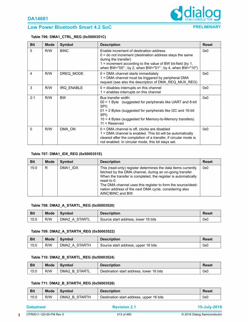
Datasheet Revision 2.1 15-July-2016
CFR0011-120-00-FM Rev 5 413 of 460 © 2016 Dialog Semiconductor
DA14681
Low Power Bluetooth Smart 4.2 SoC PRELIMINARY
5 R/W BINC Enable increment of destination address.0 = do not increment (destination address stays the same during the transfer)1 = increment according to the value of BW bit-field (by 1, when BW="00" ; by 2, when BW="01" ; by 4, when BW="10")
0x0
4 R/W DREQ_MODE 0 = DMA channel starts immediately1 = DMA channel must be triggered by peripheral DMA request (see also the description of DMA_REQ_MUX_REG)
0x0
3 R/W IRQ_ENABLE 0 = disables interrupts on this channel1 = enables interrupts on this channel
0x0
2:1 R/W BW Bus transfer width:00 = 1 Byte (suggested for peripherals like UART and 8-bit SPI)01 = 2 Bytes (suggested for peripherals like I2C and 16-bit SPI)10 = 4 Bytes (suggested for Memory-to-Memory transfers)11 = Reserved
0x0
0 R/W DMA_ON 0 = DMA channel is off, clocks are disabled1 = DMA channel is enabled. This bit will be automatically cleared after the completion of a transfer, if circular mode is not enabled. In circular mode, this bit stays set.
0x0
Table 706: DMA1_CTRL_REG (0x5000351C)
Bit Mode Symbol Description Reset
Table 707: DMA1_IDX_REG (0x5000351E)
Bit Mode Symbol Description Reset
15:0 R DMA1_IDX This (read-only) register determines the data items currently fetched by the DMA channel, during an on-going transfer. When the transfer is completed, the register is automatically reset to 0.The DMA channel uses this register to form the source/desti-nation address of the next DMA cycle, considering also AINC/BINC and BW.
0x0
Table 708: DMA2_A_STARTL_REG (0x50003520)
Bit Mode Symbol Description Reset
15:0 R/W DMA2_A_STARTL Source start address, lower 16 bits 0x0
Table 709: DMA2_A_STARTH_REG (0x50003522)
Bit Mode Symbol Description Reset
15:0 R/W DMA2_A_STARTH Source start address, upper 16 bits 0x0
Table 710: DMA2_B_STARTL_REG (0x50003524)
Bit Mode Symbol Description Reset
15:0 R/W DMA2_B_STARTL Destination start address, lower 16 bits 0x0
Table 711: DMA2_B_STARTH_REG (0x50003526)
Bit Mode Symbol Description Reset
15:0 R/W DMA2_B_STARTH Destination start address, upper 16 bits 0x0

Datasheet Revision 2.1 15-July-2016
CFR0011-120-00-FM Rev 5 414 of 460 © 2016 Dialog Semiconductor
DA14681
Low Power Bluetooth Smart 4.2 SoC PRELIMINARY
Table 712: DMA2_INT_REG (0x50003528)
Bit Mode Symbol Description Reset
15:0 R/W DMA2_INT Number of transfers until an interrupt is generated. The inter-rupt is generated after a transfer, if DMAx_INT_REG is equal to DMAx_IDX_REG and before DMAx_IDX_REG is incre-mented. The bit-field IRQ_ENABLE of DMAx_CTRL_REG must be set to '1' to let the controller generate the interrupt.
0x0
Table 713: DMA2_LEN_REG (0x5000352A)
Bit Mode Symbol Description Reset
15:0 R/W DMA2_LEN DMA channel's transfer length. DMAx_LEN of value 0, 1, 2, ... results into an actual transfer length of 1, 2, 3, ...
0x0
Table 714: DMA2_CTRL_REG (0x5000352C)
Bit Mode Symbol Description Reset
15:13 - - Reserved 0x0
12 R/W DMA_INIT 0 = DMA performs copy A1 to B1, A2 to B2, etc ...1 = DMA performs copy of A1 to B1, B2, etc ...This feature is useful for memory initialization to any value. Thus, BINC must be set to '1', while AINC is don't care, as only one fetch from A is done. This process cannot be inter-rupted by other DMA channels. It is also noted that DMA_INIT should not be used when DREQ_MODE='1'.
0x0
11 R/W DMA_IDLE 0 = Blocking mode, the DMA performs a fast back-to-back copy, disabling bus access for any bus master with lower pri-ority.1 = Interrupting mode, the DMA inserts a wait cycle after each store allowing the CPU to steal cycles or cache to per-form a burst read. If DREQ_MODE='1', DMA_IDLE is don't care.
0x0
10:8 R/W DMA_PRIO The priority level determines which DMA channel will be granted access for transferring data, in case more than one channels are active and request the bus at the same time. The greater the value, the higher the priority. In specific:000 = lowest priority111 = highest priorityIf different channels with equal priority level values request the bus at the same time, an inherent priority mechanism is applied. According to this mechanism, if, for example, both the DMA0 and DMA1 channels have the same priority level, then DMA0 will first be granted access to the bus.
0x0
7 R/W CIRCULAR 0 = Normal mode. The DMA channel stops after having com-pleted the transfer of length determined by DMAx_LEN_REG. DMA_ON automatically deasserts when the transfer is completed.1 = Circular mode (applicable only if DREQ_MODE = '1'). In this mode, DMA_ON never deasserts, as the DMA channel automatically resets DMAx_IDX_REG and starts a new transfer.
0x0
6 R/W AINC Enable increment of source address.0 = do not increment (source address stays the same during the transfer)1 = increment according to the value of BW bit-field (by 1, when BW="00" ; by 2, when BW="01" ; by 4, when BW="10")
0x0

Datasheet Revision 2.1 15-July-2016
CFR0011-120-00-FM Rev 5 415 of 460 © 2016 Dialog Semiconductor
DA14681
Low Power Bluetooth Smart 4.2 SoC PRELIMINARY
5 R/W BINC Enable increment of destination address.0 = do not increment (destination address stays the same during the transfer)1 = increment according to the value of BW bit-field (by 1, when BW="00" ; by 2, when BW="01" ; by 4, when BW="10")
0x0
4 R/W DREQ_MODE 0 = DMA channel starts immediately1 = DMA channel must be triggered by peripheral DMA request (see also the description of DMA_REQ_MUX_REG)
0x0
3 R/W IRQ_ENABLE 0 = disables interrupts on this channel1 = enables interrupts on this channel
0x0
2:1 R/W BW Bus transfer width:00 = 1 Byte (suggested for peripherals like UART and 8-bit SPI)01 = 2 Bytes (suggested for peripherals like I2C and 16-bit SPI)10 = 4 Bytes (suggested for Memory-to-Memory transfers)11 = Reserved
0x0
0 R/W DMA_ON 0 = DMA channel is off, clocks are disabled1 = DMA channel is enabled. This bit will be automatically cleared after the completion of a transfer, if circular mode is not enabled. In circular mode, this bit stays set.
0x0
Table 714: DMA2_CTRL_REG (0x5000352C)
Bit Mode Symbol Description Reset
Table 715: DMA2_IDX_REG (0x5000352E)
Bit Mode Symbol Description Reset
15:0 R DMA2_IDX This (read-only) register determines the data items currently fetched by the DMA channel, during an on-going transfer. When the transfer is completed, the register is automatically reset to 0.The DMA channel uses this register to form the source/desti-nation address of the next DMA cycle, considering also AINC/BINC and BW.
0x0
Table 716: DMA3_A_STARTL_REG (0x50003530)
Bit Mode Symbol Description Reset
15:0 R/W DMA3_A_STARTL Source start address, lower 16 bits 0x0
Table 717: DMA3_A_STARTH_REG (0x50003532)
Bit Mode Symbol Description Reset
15:0 R/W DMA3_A_STARTH Source start address, upper 16 bits 0x0
Table 718: DMA3_B_STARTL_REG (0x50003534)
Bit Mode Symbol Description Reset
15:0 R/W DMA3_B_STARTL Destination start address, lower 16 bits 0x0
Table 719: DMA3_B_STARTH_REG (0x50003536)
Bit Mode Symbol Description Reset
15:0 R/W DMA3_B_STARTH Destination start address, upper 16 bits 0x0
Datasheet Revision 2.1 15-July-2016
CFR0011-120-00-FM Rev 5 416 of 460 © 2016 Dialog Semiconductor
DA14681
Low Power Bluetooth Smart 4.2 SoC PRELIMINARY
Table 720: DMA3_INT_REG (0x50003538)
Bit Mode Symbol Description Reset
15:0 R/W DMA3_INT Number of transfers until an interrupt is generated. The inter-rupt is generated after a transfer, if DMAx_INT_REG is equal to DMAx_IDX_REG and before DMAx_IDX_REG is incre-mented. The bit-field IRQ_ENABLE of DMAx_CTRL_REG must be set to '1' to let the controller generate the interrupt.
0x0
Table 721: DMA3_LEN_REG (0x5000353A)
Bit Mode Symbol Description Reset
15:0 R/W DMA3_LEN DMA channel's transfer length. DMAx_LEN of value 0, 1, 2, ... results into an actual transfer length of 1, 2, 3, ...
0x0
Table 722: DMA3_CTRL_REG (0x5000353C)
Bit Mode Symbol Description Reset
15:13 - - Reserved 0x0
12 R/W DMA_INIT 0 = DMA performs copy A1 to B1, A2 to B2, etc ...1 = DMA performs copy of A1 to B1, B2, etc ...This feature is useful for memory initialization to any value. Thus, BINC must be set to '1', while AINC is don't care, as only one fetch from A is done. This process cannot be inter-rupted by other DMA channels. It is also noted that DMA_INIT should not be used when DREQ_MODE='1'.
0x0
11 R/W DMA_IDLE 0 = Blocking mode, the DMA performs a fast back-to-back copy, disabling bus access for any bus master with lower pri-ority.1 = Interrupting mode, the DMA inserts a wait cycle after each store allowing the CPU to steal cycles or cache to per-form a burst read. If DREQ_MODE='1', DMA_IDLE is don't care.
0x0
10:8 R/W DMA_PRIO The priority level determines which DMA channel will be granted access for transferring data, in case more than one channels are active and request the bus at the same time. The greater the value, the higher the priority. In specific:000 = lowest priority111 = highest priorityIf different channels with equal priority level values request the bus at the same time, an inherent priority mechanism is applied. According to this mechanism, if, for example, both the DMA0 and DMA1 channels have the same priority level, then DMA0 will first be granted access to the bus.
0x0
7 R/W CIRCULAR 0 = Normal mode. The DMA channel stops after having com-pleted the transfer of length determined by DMAx_LEN_REG. DMA_ON automatically deasserts when the transfer is completed.1 = Circular mode (applicable only if DREQ_MODE = '1'). In this mode, DMA_ON never deasserts, as the DMA channel automatically resets DMAx_IDX_REG and starts a new transfer.
0x0
6 R/W AINC Enable increment of source address.0 = do not increment (source address stays the same during the transfer)1 = increment according to the value of BW bit-field (by 1, when BW="00" ; by 2, when BW="01" ; by 4, when BW="10")
0x0

Datasheet Revision 2.1 15-July-2016
CFR0011-120-00-FM Rev 5 417 of 460 © 2016 Dialog Semiconductor
DA14681
Low Power Bluetooth Smart 4.2 SoC PRELIMINARY
5 R/W BINC Enable increment of destination address.0 = do not increment (destination address stays the same during the transfer)1 = increment according to the value of BW bit-field (by 1, when BW="00" ; by 2, when BW="01" ; by 4, when BW="10")
0x0
4 R/W DREQ_MODE 0 = DMA channel starts immediately1 = DMA channel must be triggered by peripheral DMA request (see also the description of DMA_REQ_MUX_REG)
0x0
3 R/W IRQ_ENABLE 0 = disables interrupts on this channel1 = enables interrupts on this channel
0x0
2:1 R/W BW Bus transfer width:00 = 1 Byte (suggested for peripherals like UART and 8-bit SPI)01 = 2 Bytes (suggested for peripherals like I2C and 16-bit SPI)10 = 4 Bytes (suggested for Memory-to-Memory transfers)11 = Reserved
0x0
0 R/W DMA_ON 0 = DMA channel is off, clocks are disabled1 = DMA channel is enabled. This bit will be automatically cleared after the completion of a transfer, if circular mode is not enabled. In circular mode, this bit stays set.
0x0
Table 722: DMA3_CTRL_REG (0x5000353C)
Bit Mode Symbol Description Reset
Table 723: DMA3_IDX_REG (0x5000353E)
Bit Mode Symbol Description Reset
15:0 R DMA3_IDX This (read-only) register determines the data items currently fetched by the DMA channel, during an on-going transfer. When the transfer is completed, the register is automatically reset to 0.The DMA channel uses this register to form the source/desti-nation address of the next DMA cycle, considering also AINC/BINC and BW.
0x0
Table 724: DMA4_A_STARTL_REG (0x50003540)
Bit Mode Symbol Description Reset
15:0 R/W DMA4_A_STARTL Source start address, lower 16 bits 0x0
Table 725: DMA4_A_STARTH_REG (0x50003542)
Bit Mode Symbol Description Reset
15:0 R/W DMA4_A_STARTH Source start address, upper 16 bits 0x0
Table 726: DMA4_B_STARTL_REG (0x50003544)
Bit Mode Symbol Description Reset
15:0 R/W DMA4_B_STARTL Destination start address, lower 16 bits 0x0
Table 727: DMA4_B_STARTH_REG (0x50003546)
Bit Mode Symbol Description Reset
15:0 R/W DMA4_B_STARTH Destination start address, upper 16 bits 0x0

Datasheet Revision 2.1 15-July-2016
CFR0011-120-00-FM Rev 5 418 of 460 © 2016 Dialog Semiconductor
DA14681
Low Power Bluetooth Smart 4.2 SoC PRELIMINARY
Table 728: DMA4_INT_REG (0x50003548)
Bit Mode Symbol Description Reset
15:0 R/W DMA4_INT Number of transfers until an interrupt is generated. The inter-rupt is generated after a transfer, if DMAx_INT_REG is equal to DMAx_IDX_REG and before DMAx_IDX_REG is incre-mented. The bit-field IRQ_ENABLE of DMAx_CTRL_REG must be set to '1' to let the controller generate the interrupt.
0x0
Table 729: DMA4_LEN_REG (0x5000354A)
Bit Mode Symbol Description Reset
15:0 R/W DMA4_LEN DMA channel's transfer length. DMAx_LEN of value 0, 1, 2, ... results into an actual transfer length of 1, 2, 3, ...
0x0
Table 730: DMA4_CTRL_REG (0x5000354C)
Bit Mode Symbol Description Reset
15:13 - - Reserved 0x0
12 R/W DMA_INIT 0 = DMA performs copy A1 to B1, A2 to B2, etc ...1 = DMA performs copy of A1 to B1, B2, etc ...This feature is useful for memory initialization to any value. Thus, BINC must be set to '1', while AINC is don't care, as only one fetch from A is done. This process cannot be inter-rupted by other DMA channels. It is also noted that DMA_INIT should not be used when DREQ_MODE='1'.
0x0
11 R/W DMA_IDLE 0 = Blocking mode, the DMA performs a fast back-to-back copy, disabling bus access for any bus master with lower pri-ority.1 = Interrupting mode, the DMA inserts a wait cycle after each store allowing the CPU to steal cycles or cache to per-form a burst read. If DREQ_MODE='1', DMA_IDLE is don't care.
0x0
10:8 R/W DMA_PRIO The priority level determines which DMA channel will be granted access for transferring data, in case more than one channels are active and request the bus at the same time. The greater the value, the higher the priority. In specific:000 = lowest priority111 = highest priorityIf different channels with equal priority level values request the bus at the same time, an inherent priority mechanism is applied. According to this mechanism, if, for example, both the DMA0 and DMA1 channels have the same priority level, then DMA0 will first be granted access to the bus.
0x0
7 R/W CIRCULAR 0 = Normal mode. The DMA channel stops after having com-pleted the transfer of length determined by DMAx_LEN_REG. DMA_ON automatically deasserts when the transfer is completed.1 = Circular mode (applicable only if DREQ_MODE = '1'). In this mode, DMA_ON never deasserts, as the DMA channel automatically resets DMAx_IDX_REG and starts a new transfer.
0x0
6 R/W AINC Enable increment of source address.0 = do not increment (source address stays the same during the transfer)1 = increment according to the value of BW bit-field (by 1, when BW="00" ; by 2, when BW="01" ; by 4, when BW="10")
0x0

Datasheet Revision 2.1 15-July-2016
CFR0011-120-00-FM Rev 5 419 of 460 © 2016 Dialog Semiconductor
DA14681
Low Power Bluetooth Smart 4.2 SoC PRELIMINARY
5 R/W BINC Enable increment of destination address.0 = do not increment (destination address stays the same during the transfer)1 = increment according to the value of BW bit-field (by 1, when BW="00" ; by 2, when BW="01" ; by 4, when BW="10")
0x0
4 R/W DREQ_MODE 0 = DMA channel starts immediately1 = DMA channel must be triggered by peripheral DMA request (see also the description of DMA_REQ_MUX_REG)
0x0
3 R/W IRQ_ENABLE 0 = disables interrupts on this channel1 = enables interrupts on this channel
0x0
2:1 R/W BW Bus transfer width:00 = 1 Byte (suggested for peripherals like UART and 8-bit SPI)01 = 2 Bytes (suggested for peripherals like I2C and 16-bit SPI)10 = 4 Bytes (suggested for Memory-to-Memory transfers)11 = Reserved
0x0
0 R/W DMA_ON 0 = DMA channel is off, clocks are disabled1 = DMA channel is enabled. This bit will be automatically cleared after the completion of a transfer, if circular mode is not enabled. In circular mode, this bit stays set.
0x0
Table 730: DMA4_CTRL_REG (0x5000354C)
Bit Mode Symbol Description Reset
Table 731: DMA4_IDX_REG (0x5000354E)
Bit Mode Symbol Description Reset
15:0 R DMA4_IDX This (read-only) register determines the data items currently fetched by the DMA channel, during an on-going transfer. When the transfer is completed, the register is automatically reset to 0.The DMA channel uses this register to form the source/desti-nation address of the next DMA cycle, considering also AINC/BINC and BW.
0x0
Table 732: DMA5_A_STARTL_REG (0x50003550)
Bit Mode Symbol Description Reset
15:0 R/W DMA5_A_STARTL Source start address, lower 16 bits 0x0
Table 733: DMA5_A_STARTH_REG (0x50003552)
Bit Mode Symbol Description Reset
15:0 R/W DMA5_A_STARTH Source start address, upper 16 bits 0x0
Table 734: DMA5_B_STARTL_REG (0x50003554)
Bit Mode Symbol Description Reset
15:0 R/W DMA5_B_STARTL Destination start address, lower 16 bits 0x0
Table 735: DMA5_B_STARTH_REG (0x50003556)
Bit Mode Symbol Description Reset
15:0 R/W DMA5_B_STARTH Destination start address, upper 16 bits 0x0

Datasheet Revision 2.1 15-July-2016
CFR0011-120-00-FM Rev 5 420 of 460 © 2016 Dialog Semiconductor
DA14681
Low Power Bluetooth Smart 4.2 SoC PRELIMINARY
Table 736: DMA5_INT_REG (0x50003558)
Bit Mode Symbol Description Reset
15:0 R/W DMA5_INT Number of transfers until an interrupt is generated. The inter-rupt is generated after a transfer, if DMAx_INT_REG is equal to DMAx_IDX_REG and before DMAx_IDX_REG is incre-mented. The bit-field IRQ_ENABLE of DMAx_CTRL_REG must be set to '1' to let the controller generate the interrupt.
0x0
Table 737: DMA5_LEN_REG (0x5000355A)
Bit Mode Symbol Description Reset
15:0 R/W DMA5_LEN DMA channel's transfer length. DMAx_LEN of value 0, 1, 2, ... results into an actual transfer length of 1, 2, 3, ...
0x0
Table 738: DMA5_CTRL_REG (0x5000355C)
Bit Mode Symbol Description Reset
15:13 - - Reserved 0x0
12 R/W DMA_INIT 0 = DMA performs copy A1 to B1, A2 to B2, etc ...1 = DMA performs copy of A1 to B1, B2, etc ...This feature is useful for memory initialization to any value. Thus, BINC must be set to '1', while AINC is don't care, as only one fetch from A is done. This process cannot be inter-rupted by other DMA channels. It is also noted that DMA_INIT should not be used when DREQ_MODE='1'.
0x0
11 R/W DMA_IDLE 0 = Blocking mode, the DMA performs a fast back-to-back copy, disabling bus access for any bus master with lower pri-ority.1 = Interrupting mode, the DMA inserts a wait cycle after each store allowing the CPU to steal cycles or cache to per-form a burst read. If DREQ_MODE='1', DMA_IDLE is don't care.
0x0
10:8 R/W DMA_PRIO The priority level determines which DMA channel will be granted access for transferring data, in case more than one channels are active and request the bus at the same time. The greater the value, the higher the priority. In specific:000 = lowest priority111 = highest priorityIf different channels with equal priority level values request the bus at the same time, an inherent priority mechanism is applied. According to this mechanism, if, for example, both the DMA0 and DMA1 channels have the same priority level, then DMA0 will first be granted access to the bus.
0x0
7 R/W CIRCULAR 0 = Normal mode. The DMA channel stops after having com-pleted the transfer of length determined by DMAx_LEN_REG. DMA_ON automatically deasserts when the transfer is completed.1 = Circular mode (applicable only if DREQ_MODE = '1'). In this mode, DMA_ON never deasserts, as the DMA channel automatically resets DMAx_IDX_REG and starts a new transfer.
0x0
6 R/W AINC Enable increment of source address.0 = do not increment (source address stays the same during the transfer)1 = increment according to the value of BW bit-field (by 1, when BW="00" ; by 2, when BW="01" ; by 4, when BW="10")
0x0

Datasheet Revision 2.1 15-July-2016
CFR0011-120-00-FM Rev 5 421 of 460 © 2016 Dialog Semiconductor
DA14681
Low Power Bluetooth Smart 4.2 SoC PRELIMINARY
5 R/W BINC Enable increment of destination address.0 = do not increment (destination address stays the same during the transfer)1 = increment according to the value of BW bit-field (by 1, when BW="00" ; by 2, when BW="01" ; by 4, when BW="10")
0x0
4 R/W DREQ_MODE 0 = DMA channel starts immediately1 = DMA channel must be triggered by peripheral DMA request (see also the description of DMA_REQ_MUX_REG)
0x0
3 R/W IRQ_ENABLE 0 = disables interrupts on this channel1 = enables interrupts on this channel
0x0
2:1 R/W BW Bus transfer width:00 = 1 Byte (suggested for peripherals like UART and 8-bit SPI)01 = 2 Bytes (suggested for peripherals like I2C and 16-bit SPI)10 = 4 Bytes (suggested for Memory-to-Memory transfers)11 = Reserved
0x0
0 R/W DMA_ON 0 = DMA channel is off, clocks are disabled1 = DMA channel is enabled. This bit will be automatically cleared after the completion of a transfer, if circular mode is not enabled. In circular mode, this bit stays set.
0x0
Table 738: DMA5_CTRL_REG (0x5000355C)
Bit Mode Symbol Description Reset
Table 739: DMA5_IDX_REG (0x5000355E)
Bit Mode Symbol Description Reset
15:0 R DMA5_IDX This (read-only) register determines the data items currently fetched by the DMA channel, during an on-going transfer. When the transfer is completed, the register is automatically reset to 0.The DMA channel uses this register to form the source/desti-nation address of the next DMA cycle, considering also AINC/BINC and BW.
0x0
Table 740: DMA6_A_STARTL_REG (0x50003560)
Bit Mode Symbol Description Reset
15:0 R/W DMA6_A_STARTL Source start address, lower 16 bits 0x0
Table 741: DMA6_A_STARTH_REG (0x50003562)
Bit Mode Symbol Description Reset
15:0 R/W DMA6_A_STARTH Source start address, upper 16 bits 0x0
Table 742: DMA6_B_STARTL_REG (0x50003564)
Bit Mode Symbol Description Reset
15:0 R/W DMA6_B_STARTL Destination start address, lower 16 bits 0x0
Table 743: DMA6_B_STARTH_REG (0x50003566)
Bit Mode Symbol Description Reset
15:0 R/W DMA6_B_STARTH Destination start address, upper 16 bits 0x0

Datasheet Revision 2.1 15-July-2016
CFR0011-120-00-FM Rev 5 422 of 460 © 2016 Dialog Semiconductor
DA14681
Low Power Bluetooth Smart 4.2 SoC PRELIMINARY
Table 744: DMA6_INT_REG (0x50003568)
Bit Mode Symbol Description Reset
15:0 R/W DMA6_INT Number of transfers until an interrupt is generated. The inter-rupt is generated after a transfer, if DMAx_INT_REG is equal to DMAx_IDX_REG and before DMAx_IDX_REG is incre-mented. The bit-field IRQ_ENABLE of DMAx_CTRL_REG must be set to '1' to let the controller generate the interrupt.
0x0
Table 745: DMA6_LEN_REG (0x5000356A)
Bit Mode Symbol Description Reset
15:0 R/W DMA6_LEN DMA channel's transfer length. DMAx_LEN of value 0, 1, 2, ... results into an actual transfer length of 1, 2, 3, ...
0x0
Table 746: DMA6_CTRL_REG (0x5000356C)
Bit Mode Symbol Description Reset
15:13 - - Reserved 0x0
12 R/W DMA_INIT 0 = DMA performs copy A1 to B1, A2 to B2, etc ...1 = DMA performs copy of A1 to B1, B2, etc ...This feature is useful for memory initialization to any value. Thus, BINC must be set to '1', while AINC is don't care, as only one fetch from A is done. This process cannot be inter-rupted by other DMA channels. It is also noted that DMA_INIT should not be used when DREQ_MODE='1'.
0x0
11 R/W DMA_IDLE 0 = Blocking mode, the DMA performs a fast back-to-back copy, disabling bus access for any bus master with lower pri-ority.1 = Interrupting mode, the DMA inserts a wait cycle after each store allowing the CPU to steal cycles or cache to per-form a burst read. If DREQ_MODE='1', DMA_IDLE is don't care.
0x0
10:8 R/W DMA_PRIO The priority level determines which DMA channel will be granted access for transferring data, in case more than one channels are active and request the bus at the same time. The greater the value, the higher the priority. In specific:000 = lowest priority111 = highest priorityIf different channels with equal priority level values request the bus at the same time, an inherent priority mechanism is applied. According to this mechanism, if, for example, both the DMA0 and DMA1 channels have the same priority level, then DMA0 will first be granted access to the bus.
0x0
7 R/W CIRCULAR 0 = Normal mode. The DMA channel stops after having com-pleted the transfer of length determined by DMAx_LEN_REG. DMA_ON automatically deasserts when the transfer is completed.1 = Circular mode (applicable only if DREQ_MODE = '1'). In this mode, DMA_ON never deasserts, as the DMA channel automatically resets DMAx_IDX_REG and starts a new transfer.
0x0
6 R/W AINC Enable increment of source address.0 = do not increment (source address stays the same during the transfer)1 = increment according to the value of BW bit-field (by 1, when BW="00" ; by 2, when BW="01" ; by 4, when BW="10")
0x0

Datasheet Revision 2.1 15-July-2016
CFR0011-120-00-FM Rev 5 423 of 460 © 2016 Dialog Semiconductor
DA14681
Low Power Bluetooth Smart 4.2 SoC PRELIMINARY
5 R/W BINC Enable increment of destination address.0 = do not increment (destination address stays the same during the transfer)1 = increment according to the value of BW bit-field (by 1, when BW="00" ; by 2, when BW="01" ; by 4, when BW="10")
0x0
4 R/W DREQ_MODE 0 = DMA channel starts immediately1 = DMA channel must be triggered by peripheral DMA request (see also the description of DMA_REQ_MUX_REG)
0x0
3 R/W IRQ_ENABLE 0 = disables interrupts on this channel1 = enables interrupts on this channel
0x0
2:1 R/W BW Bus transfer width:00 = 1 Byte (suggested for peripherals like UART and 8-bit SPI)01 = 2 Bytes (suggested for peripherals like I2C and 16-bit SPI)10 = 4 Bytes (suggested for Memory-to-Memory transfers)11 = Reserved
0x0
0 R/W DMA_ON 0 = DMA channel is off, clocks are disabled1 = DMA channel is enabled. This bit will be automatically cleared after the completion of a transfer, if circular mode is not enabled. In circular mode, this bit stays set.
0x0
Table 746: DMA6_CTRL_REG (0x5000356C)
Bit Mode Symbol Description Reset
Table 747: DMA6_IDX_REG (0x5000356E)
Bit Mode Symbol Description Reset
15:0 R DMA6_IDX This (read-only) register determines the data items currently fetched by the DMA channel, during an on-going transfer. When the transfer is completed, the register is automatically reset to 0.The DMA channel uses this register to form the source/desti-nation address of the next DMA cycle, considering also AINC/BINC and BW.
0x0
Table 748: DMA7_A_STARTL_REG (0x50003570)
Bit Mode Symbol Description Reset
15:0 R/W DMA7_A_STARTL Source start address, lower 16 bits 0x0
Table 749: DMA7_A_STARTH_REG (0x50003572)
Bit Mode Symbol Description Reset
15:0 R/W DMA7_A_STARTH Source start address, upper 16 bits 0x0
Table 750: DMA7_B_STARTL_REG (0x50003574)
Bit Mode Symbol Description Reset
15:0 R/W DMA7_B_STARTL Destination start address, lower 16 bits 0x0
Table 751: DMA7_B_STARTH_REG (0x50003576)
Bit Mode Symbol Description Reset
15:0 R/W DMA7_B_STARTH Destination start address, upper 16 bits 0x0

Datasheet Revision 2.1 15-July-2016
CFR0011-120-00-FM Rev 5 424 of 460 © 2016 Dialog Semiconductor
DA14681
Low Power Bluetooth Smart 4.2 SoC PRELIMINARY
Table 752: DMA7_INT_REG (0x50003578)
Bit Mode Symbol Description Reset
15:0 R/W DMA7_INT Number of transfers until an interrupt is generated. The inter-rupt is generated after a transfer, if DMAx_INT_REG is equal to DMAx_IDX_REG and before DMAx_IDX_REG is incre-mented. The bit-field IRQ_ENABLE of DMAx_CTRL_REG must be set to '1' to let the controller generate the interrupt.
0x0
Table 753: DMA7_LEN_REG (0x5000357A)
Bit Mode Symbol Description Reset
15:0 R/W DMA7_LEN DMA channel's transfer length. DMAx_LEN of value 0, 1, 2, ... results into an actual transfer length of 1, 2, 3, ...
0x0
Table 754: DMA7_CTRL_REG (0x5000357C)
Bit Mode Symbol Description Reset
15:13 - - Reserved 0x0
12 R/W DMA_INIT 0 = DMA performs copy A1 to B1, A2 to B2, etc ...1 = DMA performs copy of A1 to B1, B2, etc ...This feature is useful for memory initialization to any value. Thus, BINC must be set to '1', while AINC is don't care, as only one fetch from A is done. This process cannot be inter-rupted by other DMA channels. It is also noted that DMA_INIT should not be used when DREQ_MODE='1'.
0x0
11 R/W DMA_IDLE 0 = Blocking mode, the DMA performs a fast back-to-back copy, disabling bus access for any bus master with lower pri-ority.1 = Interrupting mode, the DMA inserts a wait cycle after each store allowing the CPU to steal cycles or cache to per-form a burst read. If DREQ_MODE='1', DMA_IDLE is don't care.
0x0
10:8 R/W DMA_PRIO The priority level determines which DMA channel will be granted access for transferring data, in case more than one channels are active and request the bus at the same time. The greater the value, the higher the priority. In specific:000 = lowest priority111 = highest priorityIf different channels with equal priority level values request the bus at the same time, an inherent priority mechanism is applied. According to this mechanism, if, for example, both the DMA0 and DMA1 channels have the same priority level, then DMA0 will first be granted access to the bus.
0x0
7 R/W CIRCULAR 0 = Normal mode. The DMA channel stops after having com-pleted the transfer of length determined by DMAx_LEN_REG. DMA_ON automatically deasserts when the transfer is completed.1 = Circular mode (applicable only if DREQ_MODE = '1'). In this mode, DMA_ON never deasserts, as the DMA channel automatically resets DMAx_IDX_REG and starts a new transfer.
0x0
6 R/W AINC Enable increment of source address.0 = do not increment (source address stays the same during the transfer)1 = increment according to the value of BW bit-field (by 1, when BW="00" ; by 2, when BW="01" ; by 4, when BW="10")
0x0

Datasheet Revision 2.1 15-July-2016
CFR0011-120-00-FM Rev 5 425 of 460 © 2016 Dialog Semiconductor
DA14681
Low Power Bluetooth Smart 4.2 SoC PRELIMINARY
5 R/W BINC Enable increment of destination address.0 = do not increment (destination address stays the same during the transfer)1 = increment according to the value of BW bit-field (by 1, when BW="00" ; by 2, when BW="01" ; by 4, when BW="10")
0x0
4 R/W DREQ_MODE 0 = DMA channel starts immediately1 = DMA channel must be triggered by peripheral DMA request (see also the description of DMA_REQ_MUX_REG)
0x0
3 R/W IRQ_ENABLE 0 = disables interrupts on this channel1 = enables interrupts on this channel
0x0
2:1 R/W BW Bus transfer width:00 = 1 Byte (suggested for peripherals like UART and 8-bit SPI)01 = 2 Bytes (suggested for peripherals like I2C and 16-bit SPI)10 = 4 Bytes (suggested for Memory-to-Memory transfers)11 = Reserved
0x0
0 R/W DMA_ON 0 = DMA channel is off, clocks are disabled1 = DMA channel is enabled. This bit will be automatically cleared after the completion of a transfer, if circular mode is not enabled. In circular mode, this bit stays set.
0x0
Table 754: DMA7_CTRL_REG (0x5000357C)
Bit Mode Symbol Description Reset
Table 755: DMA7_IDX_REG (0x5000357E)
Bit Mode Symbol Description Reset
15:0 R DMA7_IDX This (read-only) register determines the data items currently fetched by the DMA channel, during an on-going transfer. When the transfer is completed, the register is automatically reset to 0.The DMA channel uses this register to form the source/desti-nation address of the next DMA cycle, considering also AINC/BINC and BW.
0x0
Table 756: DMA_REQ_MUX_REG (0x50003580)
Bit Mode Symbol Description Reset
15:12 R/W DMA67_SEL Select which combination of peripherals are mapped on the DMA channels. The peripherals are mapped as pairs on two channels.Here, the first DMA request is mapped on channel 6 and the second on channel 7.See DMA01_SEL for the peripherals' mapping.
0x0
11:8 R/W DMA45_SEL Select which combination of peripherals are mapped on the DMA channels. The peripherals are mapped as pairs on two channels.Here, the first DMA request is mapped on channel 4 and the second on channel 5.See DMA01_SEL for the peripherals' mapping.
0x0
7:4 R/W DMA23_SEL Select which combination of peripherals are mapped on the DMA channels. The peripherals are mapped as pairs on two channels.Here, the first DMA request is mapped on channel 2 and the second on channel 3.See DMA01_SEL for the peripherals' mapping.
0x0

Datasheet Revision 2.1 15-July-2016
CFR0011-120-00-FM Rev 5 426 of 460 © 2016 Dialog Semiconductor
DA14681
Low Power Bluetooth Smart 4.2 SoC PRELIMINARY
3:0 R/W DMA01_SEL Select which combination of peripherals are mapped on the DMA channels. The peripherals are mapped as pairs on two channels.Here, the first DMA request is mapped on channel 0 and the second on channel 1.0x0: SPI_rx / SPI_tx0x1: SPI2_rx / SPI2_tx0x2: UART_rx / UART_tx0x3: UART2_rx / UART2_tx0x4: I2C_rx / I2C_tx0x5: I2C2_rx / I2C2_tx0x6: USB_rx / USB_tx0x7: Reserved0x8: PCM_rx / PCM_tx0x9: SRC_rx / SRC_tx (for all the supported conversions)0xA: Reserved0xB: Reserved0xC: ADC / -0xD: Reserved0xE: Reserved0xF: ReservedNote: If any of the four available peripheral selector fields (DMA01_SEL, DMA23_SEL, DMA45_SEL, DMA67_SEL) have the same value, the lesser significant selector has higher priority and will control the dma acknowledge. Hence, if DMA01_SEL = DMA23_SEL, the channels 0 and 1 will generate the DMA acknowledge signals for the selected peripheral. Consequently, it is suggested to assign the intended peripheral value to a unique selector field.
0x0
Table 756: DMA_REQ_MUX_REG (0x50003580)
Bit Mode Symbol Description Reset
Table 757: DMA_INT_STATUS_REG (0x50003582)
Bit Mode Symbol Description Reset
15:8 - - Reserved 0x0
7 R DMA_IRQ_CH7 0 = IRQ on channel 7 is not set1 = IRQ on channel 7 is set
0x0
6 R DMA_IRQ_CH6 0 = IRQ on channel 6 is not set1 = IRQ on channel 6 is set
0x0
5 R DMA_IRQ_CH5 0 = IRQ on channel 5 is not set1 = IRQ on channel 5 is set
0x0
4 R DMA_IRQ_CH4 0 = IRQ on channel 4 is not set1 = IRQ on channel 4 is set
0x0
3 R DMA_IRQ_CH3 0 = IRQ on channel 3 is not set1 = IRQ on channel 3 is set
0x0
2 R DMA_IRQ_CH2 0 = IRQ on channel 2 is not set1 = IRQ on channel 2 is set
0x0
1 R DMA_IRQ_CH1 0 = IRQ on channel 1 is not set1 = IRQ on channel 1 is set
0x0
0 R DMA_IRQ_CH0 0 = IRQ on channel 0 is not set1 = IRQ on channel 0 is set
0x0

Datasheet Revision 2.1 15-July-2016
CFR0011-120-00-FM Rev 5 427 of 460 © 2016 Dialog Semiconductor
DA14681
Low Power Bluetooth Smart 4.2 SoC PRELIMINARY
Table 758: DMA_CLEAR_INT_REG (0x50003584)
Bit Mode Symbol Description Reset
15:8 - - Reserved 0x0
7 R0/W DMA_RST_IRQ_CH7 Writing a 1 will reset the IRQ of channel 7 ; writing a 0 will have no effect.
0x0
6 R0/W DMA_RST_IRQ_CH6 Writing a 1 will reset the IRQ of channel 6 ; writing a 0 will have no effect.
0x0
5 R0/W DMA_RST_IRQ_CH5 Writing a 1 will reset the IRQ of channel 5 ; writing a 0 will have no effect.
0x0
4 R0/W DMA_RST_IRQ_CH4 Writing a 1 will reset the IRQ of channel 4 ; writing a 0 will have no effect.
0x0
3 R0/W DMA_RST_IRQ_CH3 Writing a 1 will reset the IRQ of channel 3 ; writing a 0 will have no effect.
0x0
2 R0/W DMA_RST_IRQ_CH2 Writing a 1 will reset the IRQ of channel 2 ; writing a 0 will have no effect.
0x0
1 R0/W DMA_RST_IRQ_CH1 Writing a 1 will reset the IRQ of channel 1 ; writing a 0 will have no effect.
0x0
0 R0/W DMA_RST_IRQ_CH0 Writing a 1 will reset the IRQ of channel 0 ; writing a 0 will have no effect.
0x0

Datasheet Revision 2.1 15-July-2016
CFR0011-120-00-FM Rev 5 428 of 460 © 2016 Dialog Semiconductor
DA14681
Low Power Bluetooth Smart 4.2 SoC PRELIMINARY
37.27 APU REGISTER FILE
Table 759: Register map APU
Address Port Description
0x50004000 SRC1_CTRL_REG SRC1 control register
0x50004004 SRC1_IN_FS_REG SRC1 Sample input rate
0x50004008 SRC1_OUT_FS_REG SRC1 Sample output rate
0x5000400C SRC1_IN1_REG SRC1 data in 1
0x50004010 SRC1_IN2_REG SRC1 data in 2
0x50004014 SRC1_OUT1_REG SRC1 data out 1
0x50004018 SRC1_OUT2_REG SRC1 data out 2
0x5000401C APU_MUX_REG APU mux register
0x50004020 COEF10_SET1_REG SRC coefficient 1,0 set 1
0x50004024 COEF32_SET1_REG SRC coefficient 3,2 set 1
0x50004028 COEF54_SET1_REG SRC coefficient 5,4 set 1
0x5000402C COEF76_SET1_REG SRC coefficient 7,6 set 1
0x50004030 COEF98_SET1_REG SRC coefficient 9,8 set 1
0x50004034 COEF0A_SET1_REG SRC coefficient 10 set 1
0x50004100 PCM1_CTRL_REG PCM1 Control register
0x50004104 PCM1_IN1_REG PCM1 data in 1
0x50004108 PCM1_IN2_REG PCM1 data in 2
0x5000410C PCM1_OUT1_REG PCM1 data out 1
0x50004110 PCM1_OUT2_REG PCM1 data out 2
Table 760: SRC1_CTRL_REG (0x50004000)
Bit Mode Symbol Description Reset
31:30 - - Reserved 0
29:28 R/W SRC_PDM_MODE PDM Output mode selection on PDM_DO100: No output01: Right channel (falling edge of PDM_CLK)10: Left channel (rising edge of PDM_CLK)11: Left and Right channel
0
27:26 - - Reserved 0
25 W SRC_OUT_FLOWCLR
Writing a 1 clears the SRC1_OUT Overflow/underflow bits 23-22. No more over/underflow indications while bit is 1. Keep 1 until the over/under flow bit is cleared
0
24 W SRC_IN_FLOWCLR Writing a 1 clears the SRC1_IN Overflow/underflow bits 21-20. No more over/underflow indications while bit is 1. Keep 1 until the over/under flow bit is cleared
0
23 R SRC_OUT_UNFLOW 1 = SRC1_OUT Underflow occurred 0
22 R SRC_OUT_OVFLOW 1 = SRC1_OUT Overflow occurred 0
21 R SRC_IN_UNFLOW 1 = SRC1_IN Underflow occurred 0
20 R SRC_IN_OVFLOW 1 = SRC1_IN Overflow occurred 0
19 - - Reserved 0
18 R SRC_OUT_OK SRC1_OUT Status0: acquisition in progress1: acquisition ready (In manual mode this bit is always 1)
0

Datasheet Revision 2.1 15-July-2016
CFR0011-120-00-FM Rev 5 429 of 460 © 2016 Dialog Semiconductor
DA14681
Low Power Bluetooth Smart 4.2 SoC PRELIMINARY
17:16 R/W SRC_OUT_US SRC1_OUT UpSampling IIR filters setting00: for sample rates up-to 48kHz01: for sample rates of 96kHz10: reserved11: for sample rates of 192kHz
0
15 - - Reserved 0
14 R/W SRC_OUT_CAL_BYPASS
SRC1_OUT1 upsampiling filter bypass0:Do not bypass1:Bypass filter
0
13 R/W SRC_OUT_AMODE SRC1_OUT1 Automatic Conversion mode0:Manual mode1:Automatic mode
0
12:10 - - Reserved 0
9:8 - - Reserved 0
7 R/W SRC_DITHER_DISABLE
Dithering feature0: Enable1: Disable
0
6 R SRC_IN_OK SRC1_IN status0: Acquisition in progress1: Acquisition ready
0
5:4 R/W SRC_IN_DS SRC1_IN UpSampling IIR filters setting00: for sample rates up-to 48kHz01: for sample rates of 96kHz10: reserved11: for sample rates of 192kHz
0
3 - - Reserved 0
2 R/W SRC_IN_CAL_BYPASS
SRC1_IN upsampeling filter bypass0: Do not bypass1: Bypass filter
0
1 R/W SRC_IN_AMODE SRC1_IN Automatic conversion mode0: Manual mode1: Automatic mode
0
0 R/W SRC_EN SRC1_IN and SRC1_OUT enable0: disabled1: enabled
0
Table 760: SRC1_CTRL_REG (0x50004000)
Bit Mode Symbol Description Reset
Table 761: SRC1_IN_FS_REG (0x50004004)
Bit Mode Symbol Description Reset
31:24 - - Reserved 0

Datasheet Revision 2.1 15-July-2016
CFR0011-120-00-FM Rev 5 430 of 460 © 2016 Dialog Semiconductor
DA14681
Low Power Bluetooth Smart 4.2 SoC PRELIMINARY
23:0 R/W SRC_IN_FS SRC_IN Sample rateSRC_IN_FS = 8192*Sample_rate/100Sample_rate upper limit is 192 kHz. For 96 kHz and 192 kHz SRC_CTRLx_REG[SRC_IN_DS] must be set as shown below:Sample_rate SRC_IN_FS SRC_IN_DS Audio BW8000 Hz 0xA0000 0 4000 Hz11025 Hz 0x0DC800 0 5512 Hz16000 Hz 0x140000 0 8000 Hz22050 Hz 0x1B9000 0 11025 Hz32000 Hz 0x280000 0 16000 Hz44100 Hz 0x372000 0 22050 Hz48000 Hz 0x3C0000 0 24000 Hz96000 Hz 0x3C0000 1 24000 Hz192000 Hz 0x3C0000 3 24000 HzIn manual SRC mode, SRC_IN_FS can be set and adjusted to the desired sample rate at any time.In automatic mode the SRC returns the final sample rate as soon as SRC_IN_OK. Note that SRC_DS is not calculated in automatic mode and must be set manually automatic mode with Sample_rate of 96 kHz and 192 kHz.
0
Table 761: SRC1_IN_FS_REG (0x50004004)
Bit Mode Symbol Description Reset
Table 762: SRC1_OUT_FS_REG (0x50004008)
Bit Mode Symbol Description Reset
31:24 - - Reserved 0
23:0 R/W SRC_OUT_FS SRC_OUT Sample rateSRC_OUT_FS = 8192*Sample_rate/100Sample_rate upper limit is 192 kHz. For 96 kHz and 192 kHz SRC_CTRLx_REG[SRC_DS] must be set as shown below:Sample_rate SRC_OUT_FS SRC_OUT_DS Audio BW8000 Hz 0xA0000 0 4000 Hz11025 Hz 0x0DC800 0 5512 Hz16000 Hz 0x140000 0 8000 Hz22050 Hz 0x1B9000 0 11025 Hz32000 Hz 0x280000 0 16000 Hz44100 Hz 0x372000 0 22050 Hz48000 Hz 0x3C0000 0 24000 Hz96000 Hz 0x3C0000 1 24000 Hz192000 Hz 0x3C0000 3 24000 HzIn manual SRC mode, SRC_OUT_FS can be set and adjusted to the desired sample rate at any time.In automatic mode the SRC returns the final sample rate as soon as SRC_OUT_OK. Note that SRC_DS is not calculated in automatic mode and must be set manually automatic mode with Sample_rate of 96 kHz and 192 kHz.
0
Table 763: SRC1_IN1_REG (0x5000400C)
Bit Mode Symbol Description Reset
31:8 R/W SRC_IN SRC1_IN1 0

Datasheet Revision 2.1 15-July-2016
CFR0011-120-00-FM Rev 5 431 of 460 © 2016 Dialog Semiconductor
DA14681
Low Power Bluetooth Smart 4.2 SoC PRELIMINARY
Table 764: SRC1_IN2_REG (0x50004010)
Bit Mode Symbol Description Reset
31:8 R/W SRC_IN SRC1_IN2 0
Table 765: SRC1_OUT1_REG (0x50004014)
Bit Mode Symbol Description Reset
31:8 R SRC_OUT SRC1_OUT1 0
Table 766: SRC1_OUT2_REG (0x50004018)
Bit Mode Symbol Description Reset
31:8 R SRC_OUT SRC1_OUT2 0
Table 767: APU_MUX_REG (0x5000401C)
Bit Mode Symbol Description Reset
6 R/W PDM1_MUX_IN PDM1 input mux0 = SRC1_MUX_IN1 = PDM input
0x0
5:3 R/W PCM1_MUX_IN PCM1 input mux0 = off1 = SRC1 output2 = PCM output registers
0x0
2:0 R/W SRC1_MUX_IN SRC1 input mux0 = off1 = PCM output2 = SRC1 input registers
0x0
Table 768: COEF10_SET1_REG (0x50004020)
Bit Mode Symbol Description Reset
31:16 R/W SRC_COEF1 coefficient 1 0x79A9
15:0 R/W SRC_COEF0 coefficient 0 0x9278
Table 769: COEF32_SET1_REG (0x50004024)
Bit Mode Symbol Description Reset
31:16 R/W SRC_COEF3 coefficient 3 0x6D56
15:0 R/W SRC_COEF2 coefficient 2 0x8B41
Table 770: COEF54_SET1_REG (0x50004028)
Bit Mode Symbol Description Reset
31:16 R/W SRC_COEF5 coefficient 5 0x9BC5
15:0 R/W SRC_COEF4 coefficient 4 0xBE15

Datasheet Revision 2.1 15-July-2016
CFR0011-120-00-FM Rev 5 432 of 460 © 2016 Dialog Semiconductor
DA14681
Low Power Bluetooth Smart 4.2 SoC PRELIMINARY
Table 771: COEF76_SET1_REG (0x5000402C)
Bit Mode Symbol Description Reset
31:16 R/W SRC_COEF7 coefficient 7 0x8C28
15:0 R/W SRC_COEF6 coefficient 6 0x7E1A
Table 772: COEF98_SET1_REG (0x50004030)
Bit Mode Symbol Description Reset
31:16 R/W SRC_COEF9 coefficient 9 0x92D7
15:0 R/W SRC_COEF8 coefficient 8 0x75E6
Table 773: COEF0A_SET1_REG (0x50004034)
Bit Mode Symbol Description Reset
15:0 R/W SRC_COEF10 coefficient 10 0x41F2
Table 774: PCM1_CTRL_REG (0x50004100)
Bit Mode Symbol Description Reset
31:20 R/W PCM_FSC_DIV PCM Framesync divider, Values 7-0xFFF. To divide by N, write N-1. (Minimum value N-1=7 for 8 bits PCM_FSC)Note if PCM_CLK_BIT=1, N must always be even
0x0
19:17 - - Reserved 0x0
16 R/W PCM_FSC_EDGE 0: shift channels 1, 2, 3, 4, 5, 6, 7, 8 after PCM_FSC edge1: shift channels 1, 2, 3, 4 after PCM_FSC edge shift chan-nels 5, 6, 7, 8 after opposite PCM_FSC edge
0x0
15:11 R/W PCM_CH_DEL Channel delay in multiples of 8 bits 0x0
10 R/W PCM_CLK_BIT 0:One clock cycle per data bit1:Two cloc cycles per data bit
0x0
9 R/W PCM_FSCINV 0: PCM FSC1: PCM FSC inverted
0x0
8 R/W PCM_CLKINV 0:PCM CLK1:PCM CLK inverted
0x0
7 R/W PCM_PPOD 0:PCM DO push pull1:PCM DO open drain
0x0
6 R/W PCM_FSCDEL 0:PCM FSC starts one cycle before MSB bit1:PCM FSC starts at the same time as MSB bit
0x0
5:2 R/W PCM_FSCLEN 0:PCM FSC length equal to 1 data bitN:PCM FSC length equal to N*8
0x0
1 R/W PCM_MASTER 0:PCM interface in slave mode1:PCM interface in master mode
0x0
0 R/W PCM_EN 0:PCM interface disabled1:PCM interface enabled
0x0
Table 775: PCM1_IN1_REG (0x50004104)
Bit Mode Symbol Description Reset
31:0 R PCM_IN PCM1_IN1 bits 31-0 0xFFFFFFFF

Datasheet Revision 2.1 15-July-2016
CFR0011-120-00-FM Rev 5 433 of 460 © 2016 Dialog Semiconductor
DA14681
Low Power Bluetooth Smart 4.2 SoC PRELIMINARY
Table 776: PCM1_IN2_REG (0x50004108)
Bit Mode Symbol Description Reset
31:0 R PCM_IN PCM1_IN2 bits 31-0 0xFFFFFFFF
Table 777: PCM1_OUT1_REG (0x5000410C)
Bit Mode Symbol Description Reset
31:0 R/W PCM_OUT PCM1_OUT1 bits 31-0 0xFFFFFFFF
Table 778: PCM1_OUT2_REG (0x50004110)
Bit Mode Symbol Description Reset
31:0 R/W PCM_OUT PCM1_OUT2 bits 31-0 0xFFFFFFFF

Datasheet Revision 2.1 15-July-2016
CFR0011-120-00-FM Rev 5 434 of 460 © 2016 Dialog Semiconductor
DA14681
Low Power Bluetooth Smart 4.2 SoC PRELIMINARY
37.28 TRNG REGISTER FILE
Table 779: Register map TRNG
Address Port Description
0x50005000 TRNG_CTRL_REG TRNG control register
0x50005004 TRNG_FIFOLVL_REG TRNG FIFO level register
0x50005008 TRNG_VER_REG TRNG Version register
Table 780: TRNG_CTRL_REG (0x50005000)
Bit Mode Symbol Description Reset
31:2 - - Reserved 0x0
1 R/W TRNG_MODE 0: select the TRNG with asynchronous free running oscilla-tors (default)1: select the pseudo-random generator with synchronous oscillators (for simulation purpose only)
0x0
0 R/W TRNG_ENABLE 0: Disable the TRNG1: Enable the TRNG this signal is ignored when the FIFO is full
0x0
Table 781: TRNG_FIFOLVL_REG (0x50005004)
Bit Mode Symbol Description Reset
31:6 - - Reserved 0x0
5 R TRNG_FIFOFULL 1:FIFO full indication. This bit is cleared if the FIFO is read. 0x0
4:0 R TRNG_FIFOLVL Number of 32 bit words of random data in the FIFO (max 31) until the FIFO is full. When it is 0 and TRNG_FIFOFULL is 1, it means the FIFO is full.
0x0
Table 782: TRNG_VER_REG (0x50005008)
Bit Mode Symbol Description Reset
31:24 R TRNG_MAJ Major version number 0x0
23:16 R TRNG_MIN Minor version number 0x0
15:0 R TRNG_SVN SVN revision number 0x103

Datasheet Revision 2.1 15-July-2016
CFR0011-120-00-FM Rev 5 435 of 460 © 2016 Dialog Semiconductor
DA14681
Low Power Bluetooth Smart 4.2 SoC PRELIMINARY
37.29 ELLIPTIC CURVE CONTROLLER REGISTER FILE
Table 783: Register map Elliptic Curve Controller
Address Port Description
0x50006000 ECC_CONFIG_REG Configuration register
0x50006004 ECC_COMMAND_REG Command register
0x50006008 ECC_CONTROL_REG Control register
0x5000600C ECC_STATUS_REG Status register
0x50006010 ECC_VERSION_REG Version register
Table 784: ECC_CONFIG_REG (0x50006000)
Bit Mode Symbol Description Reset
20:16 R/W ECC_OPPTRC When executing primitive arithmetic operations, this pointer defines the location where the result will be stored in Mem-ory.
0x0
15:13 - - Reserved 0x0
12:8 R/W ECC_OPPTRB When executing primitive arithmetic operations, this Pointer defines where operand B is located in memory.
0x0
7:5 - - Reserved 0x0
4:0 R/W ECC_OPPTRA When executing primitive arithmetic operations, this Pointer defines where operand A is located in memory.
0x0
Table 785: ECC_COMMAND_REG (0x50006004)
Bit Mode Symbol Description Reset
31 R/W ECC_CALCR2 This bit indicates if the IP has to calculate R mod N for the next operation. This bit must be set to 1 when a new prime number has been programmed. This bit is automatically cleared when R mod N has been calculated.'0': no effect'1': forces the IP to re-calculate R mod N
0x0
30 R/W ECC_SIGNB Sign of parameter B in equation y2=x3+Ax+B'0': B is positive'1': B is negative
0x0
29 R/W ECC_SIGNA Sign of parameter A in equation y2=x3+Ax+B'0': A is positive'1': A is negative
0x0
28:16 - - Reserved 0x0
15:8 R/W ECC_SIZEOFOPERANDS
This field defines the size (= number of 64-bit double words) of the operands for the current operation. Possible values are limited by the generic parameter g_Log2MaxDataSize that defines the max space allocated or reserved to each operand.Arbitrary Data/Key size from 128 up to 2566 are supported:0x02 (02d) -> 128-bit Data/Key size0x03 (02d) -> 256-bit Data/Key sizeECC-ECDSA - Prime Field F(p)0x03 -> 192-bit (Curve P-192)0x04 -> 256-bit (Curves P-224 & P-256)ECC-ECDSA - Binary Field F(2m)0x03 -> 192-bit (Curve K-163)0x04 -> 256-bit (Curve K-233)- 4 Xers: 0x01, 0x02, 0x4, 0x6 -> 64, 128 & multiples of 128 bits
0x0

Datasheet Revision 2.1 15-July-2016
CFR0011-120-00-FM Rev 5 436 of 460 © 2016 Dialog Semiconductor
DA14681
Low Power Bluetooth Smart 4.2 SoC PRELIMINARY
7 R/W ECC_FIELD '0': Field is F(p)'1': Field is F(2m)
0x0
6:0 R/W ECC_TYPEOPERATION
Primitive Arithmetic Operations F(p) & F(2m)[6:4] = 0x0[3:0] =0x0 -> Reserved0x1 -> Modular Addition0x2 -> Modular Subtraction0x3 -> Modular Multiplication (Odd N)0x4 -> Modular Reduction (Odd N)0x5 -> Modular Division (Odd N)0x6 -> Modular Inversion (Odd N)0x7 -> Reserved0x8 -> Multiplication0x9 -> Modular Inversion (Even N)0xA -> Modular Reduction (Even N)others -> ReservedC = A + B mod NC = A - B mod NC = A * B mod NC = B mod NC = A/B mod NC = 1/B mod NC = A * BC = 1/B mod NC = B mod NHigh-level RSA, CRT & DSA Operations - F(p) only([7] forced to 0)[6:4] = 0x1[3:0] =0x0 -> MulModN0x1 -> MulAddN0x2 -> ECMQV (part1)others -> ReservedPrimitive ECC & Check Point Operations F(p) & F(2m)[6:4] = 0x2[3:0] =0x0 -> Point Doubling (Projective Coord.)0x1 -> ptAdd30x2 -> GenSessionKey0x3 -> Check_AB (ECDSA)0x4 -> Check_n (ECDSA)0x5 -> Check single value less than N0x6 -> Check_Point_On_Curve0x7-> Reserved0x8 -> Curve25519 point multiplication0x9 -> Ed25519 Check point on curve0xA -> Ed25519 ScalarMult0xB -> Ed25519 CheckValidothers -> Reserved(continued on next page)
0x0
Table 785: ECC_COMMAND_REG (0x50006004)
Bit Mode Symbol Description Reset

Datasheet Revision 2.1 15-July-2016
CFR0011-120-00-FM Rev 5 437 of 460 © 2016 Dialog Semiconductor
DA14681
Low Power Bluetooth Smart 4.2 SoC PRELIMINARY
6:0 R/W ECC_TYPEOPERATION
(continued)
High-level ECC ECDSA Operations F(p) & F(2m)[6:4] = 0x3[3:0] =0x0 -> ECMQV (part 2)0x1 -> Verify ZKP0x2 -> ECDSA Domain Parameters Validationothers -> Reserved[6:4]=0x4, 0x5, 0x6, 0x7 -> Reserved
0x0
Table 785: ECC_COMMAND_REG (0x50006004)
Bit Mode Symbol Description Reset
Table 786: ECC_CONTROL_REG (0x50006008)
Bit Mode Symbol Description Reset
0 R/W ECC_START The Start signal is activated when all data and key inputs have been loaded in the external crypto memory and are available for processing. This signal is active high and is sampled on the rising edge of Clk.When this signal goes high, the PK Command present in the PK_CommandReg[] is initiated and executed. The PK_Start signal is ignored when the core is already processing data and is automatically cleared when the operation is finished
0x0
Table 787: ECC_STATUS_REG (0x5000600C)
Bit Mode Symbol Description Reset
16 R ECC_BUSY This Status Signal indicates that the core is processing data. This signal is active high and goes low when the selected algorithm is finished.
0x0
15:13 - - Reserved 0x0
12 R ECC_PRIMALITYTESTRESULT
After the Miller-Rabin Primality test, this flag is:- set to 0 when the random number under test is probably prime- cleared to 1 when the random number under test is com-posite
0x0
11 R ECC_NOTINVERTIBLE
This flag is set to 1 when executing a modular inversion (PK_CommandReg[3:0] = 0x6 or 0x9) if the operand is not invertible.
0x0
10 R ECC_PARAM_AB_NOTVALID
Status signal set to 1 when parameters A and B are not valid, i.e 4A+ 27B = 0. This flag is updated after execution of the command Check_AB.
0x0
9 R ECC_SIGNATURE_NOTVALID
This flag indicates if the signature can be accepted or must be rejected.This flag is set to 1 when the signature is not valid and is updated after execution of the command ECDSA_Generation, ECDSA_Verification, DSA_Generation, DSA_Verification.
0x0
8 - - Reserved 0x0
7 R ECC_PARAM_N_NOTVALID
Status signal set to 1 when Parameter n is not valid.This flag is updated after execution of the command Check_n.
0x0
6 R ECC_COUPLE_NOTVALID
Status signal set to 1 when couple x, y is not valid (i.e. not smaller than the prime).This flag is updated after execution of the command Check_Couple_Less_Prime.
0x0

Datasheet Revision 2.1 15-July-2016
CFR0011-120-00-FM Rev 5 438 of 460 © 2016 Dialog Semiconductor
DA14681
Low Power Bluetooth Smart 4.2 SoC PRELIMINARY
5 R ECC_POINT_PX_ATINFINITY
Status signal set to 1 when Point Px is at the infinity.This flag is updated after execution of an ECC operation.
0x0
4 R ECC_POINT_PX_NOTONCURVE
Status signal set to 1 when Point Px is not on the defined EC. This flag is updated after execution of the command Check_Point_OnCurve.
0x0
3:0 R ECC_FAIL_ADDRESS
Address of the last Point detected as Not On Curve, Not Valid or at the infinity.
0x0
Table 787: ECC_STATUS_REG (0x5000600C)
Bit Mode Symbol Description Reset
Table 788: ECC_VERSION_REG (0x50006010)
Bit Mode Symbol Description Reset
15:8 R ECC_HVN Version of IP to be read via CPU interface. 0x4
7:0 R ECC_SVN Version of Crypto code to be read via CPU interface.Note that this should be read before ECC is used since it corrupts its contents.
0x0

Datasheet Revision 2.1 15-July-2016
CFR0011-120-00-FM Rev 5 439 of 460 © 2016 Dialog Semiconductor
DA14681
Low Power Bluetooth Smart 4.2 SoC PRELIMINARY
38 SpecificationsAll MIN/MAX specification limits are guaranteed by design, production testing and/or statistical characterisation. Typ-ical values are based on characterisation results at default measurement conditions and are informative only.
Default measurement conditions (unless otherwise specified): VBAT1 = VBAT2 = 3.0 V, TA = 25 C. All radio measure-ments are performed with standard RF measurement equipment providing a source/load impedance of 50 .

Datasheet Revision 2.1 15-July-2016
CFR0011-120-00-FM Rev 5 440 of 460 © 2016 Dialog Semiconductor
DA14681
Low Power Bluetooth Smart 4.2 SoC PRELIMINARY
Table 789: Absolute maximum ratings
Parameter Description Conditions Min Typ Max Unit
VPIN_LIM_DEF limiting voltage on a pin default, unless other-wise specified
-0.1 3.6 V
VBAT_LIM limiting battery supply voltage
pin VBAT 0 5 V
VBUS_LIM limiting bus supply volt-age
pin VBUS 0 6.5 V
tR_SUP power supply rise time 30 ms
VPIN_LIM_3V3 limiting voltage on a pin 3.3 V I/O pins 0 3.45 V
VPIN_LIM_1V8 limiting voltage on a pin 1.8 V I/O pins 0 1.98 V
VESD_HBM_QFN
60
electrostatic discharge voltage (Human Body Model)
QFN60 package 2000 V
VESD_CDM_QFN
60
electrostatic discharge voltage (Charged Device Model)
QFN60 package 500 V
TSTG storage temperature -50 150 °C
Table 790: Recommended operating conditions
Parameter Description Conditions Min Typ Max Unit
VBAT battery supply voltage pin VBAT1 and VBAT2 1.7 4.75 V
VBAT_OTP V33 rail supply voltage Voltage range for OTP programming. Required temperature for pro-gramming is between -
20oC and 85oC
2.25 3.6 V
VBUS bus supply voltage pin VBUS 4.2 5.75 V
VPIN_3V3 voltage on a pin 3.3 V I/O pins 0 3.3 V
VPIN_1V8 voltage on a pin 1.8 V I/O pins 0 1.8 V
TA ambient temperature -40 85 °C
Table 791: DC characteristics
Parameter Description Conditions Min Typ Max Unit
IBAT_IDLE battery supply current CPU is idle (Wait for Interrupt - WFI); sys_clk = 16 MHz; pclk = 2 MHz; DC-DC on; FLASH off; peripherals on; VBAT = 3 V.
0.4 0.6 1 mA
IBAT_RUN_16MHz battery supply current CPU is executing code from 32 kB RAM; sys_clk = 16 MHz; pclk=2 MHz; DC-DC on; FLASH off; peripherals on; VBAT = 3 V.
1.2 1.4 1.9 mA

Datasheet Revision 2.1 15-July-2016
CFR0011-120-00-FM Rev 5 441 of 460 © 2016 Dialog Semiconductor
DA14681
Low Power Bluetooth Smart 4.2 SoC PRELIMINARY
IBAT_RUN_48MHz battery supply current CPU is executing code from 32 kB RAM; sys_clk = 48 MHz; pclk = 2 MHz; DC-DC on; FLASH off. PLL on; peripherals on; VBAT = 3 V.
3.5 3.9 4.4 mA
IBAT_RUN_96MHz battery supply current CPU is executing code from 32 kB RAM; sys_clk = 96 MHz; pclk = 2 MHz; DC-DC on; FLASH off; PLL on; peripherals on; VBAT = 3 V.
5.7 6.2 6.9 mA
IBAT_HIBERN battery supply current Hibernation mode; no RAM retained; RCX clock on; VBAT_RET on; DC-DC off; VDD_RET = 0.9 V; FLASH off; VBAT = 3 V.
1.4 A
IBAT_DP_SLP_8K battery supply current Deep Sleep mode; 8 kB RAM retained; RCX clock on; VBAT_RET on; DC-DC off; VDD_RET = 0.9 V; FLASH off; VBAT = 3 V.
1.8 A
IBAT_DP_SLP_24
K
battery supply current Deep Sleep mode; 24 kB RAM retained; aRCX clock on; VBAT_RET on; DC-DC off; VDD_RET = 0.9 V; FLASH off; VBAT = 3 V.
2.4 A
IBAT_EX_SLP_16
K_32K_FP
battery supply current Extended Sleep mode; 16 kB (code) and 32 kB (data) RAM retained; XTAL32K on; DC-DC off; VDD_RET = 0.9 V; FLASH in Power Down mode; VBAT = 3 V.
1.7 2.6 14.7 A
IBAT_EX_SLP_16
K_128K_FP
battery supply current Extended Sleep mode; 16 kB cache and 128 kB (data) RAM retained; XTAL32K on; DC-DC off; VDD_RET = 0.9 V; FLASH in Power Down mode; VBAT = 3 V.
2.3 4.5 38.4 A
IBAT_BLE_RX_16
M_FS
battery supply current BLE receive mode; fCLK = 16 MHz; DC-DC on; FLASH in Standby mode; VBAT= 3 V.
5.7 5.8 7 mA
IBAT_BLE_TX_16
M_FS
battery supply current BLE transmit mode; fCLK = 16 MHz; DC-DC on; FLASH in Standby mode; VBAT = 3 V.
5.7 5.9 6.5 mA
Table 791: DC characteristics
Parameter Description Conditions Min Typ Max Unit

Datasheet Revision 2.1 15-July-2016
CFR0011-120-00-FM Rev 5 442 of 460 © 2016 Dialog Semiconductor
DA14681
Low Power Bluetooth Smart 4.2 SoC PRELIMINARY
IBAT_BLE_RX_96
M_FS
battery supply current BLE receive mode; fCLK = 96 MHz; DC-DC on; FLASH in Standby mode; VBAT = 3 V.
8.2 8.5 9.5 mA
IBAT_BLE_TX_96
M_FS
battery supply current BLE transmit mode; fCLK = 96 MHz; DC-DC on; FLASH in Standby mode; VBAT = 3 V.
8.4 8.1 9 mA
Table 792: Timing characteristics
Parameter Description Conditions Min Typ Max Unit
tSTA_SUP supply startup time time from power-on reset or wake-up to BootROM/application execution start
2000 s
tSTA_BOOT booter startup time BootROM code execu-tion time
20 ms
tCLF_OTP cache line fetch time from OTP; line size = 8 B 6 clock
tCLF_FLA cache line fetch time from FLASH; line size = 8 B
40 clock
Table 793: Thermal characteristics
Parameter Description Conditions Min Typ Max Unit
RTH_J-A_sPCB Device thermal resist-ance junction to ambient
aQFN60 package; Non-standard PCB; Zero number of thermal vias (worst case);
56.9 °C/W
RTH_J-A_jPCB Device thermal resist-ance junction to ambient
aQFN60 package; JEDEC standard PCB; Zero number of thermal vias (worst case);
40 °C/W
Table 794: 16 MHz Crystal Oscillator: Recommended operating conditions
Parameter Description Conditions Min Typ Max Unit
fXTAL(16M) crystal oscillator fre-quency
16 MHz
ESR(16M) equivalent series resist-ance
100
CL(16M) load capacitance No external capacitors are required.
4 10 12 pF
C0(16M) shunt capacitance No external capacitors are required.
5 pF
fXTAL(16M) crystal frequency toler-ance
After optional trimming; including aging and tem-perature drift(Note 21)
-20 20 ppm
Table 791: DC characteristics
Parameter Description Conditions Min Typ Max Unit

Datasheet Revision 2.1 15-July-2016
CFR0011-120-00-FM Rev 5 443 of 460 © 2016 Dialog Semiconductor
DA14681
Low Power Bluetooth Smart 4.2 SoC PRELIMINARY
Note 21: Using the internal varicaps a wide range of crystals can be trimmed to the required tolerance.
Note 22: Maximum allowed frequency tolerance for compensation by the internal varicap trimming mechanism.
Note 23: Select a crystal which can handle a drive level of at least this specification.
Note 24: Select a crystal that can handle a drive level of at least this specification.
fX-
TAL(16M)UNTcrystal frequency toler-ance
Untrimmed; including aging and temperature drift(Note 22)
-40 40 ppm
PDRV(MAX)(16M)
maximum drive power (Note 23) 100 W
VCLK(EXT)(16M) external clock voltage In case of external clock source on XTAL16Mp (XTAL16Mm floating or connected to mid-level 0.6 V)
1 1.2 V
N(EXTER-NAL)16M
phase noise fC = 50 kHz; in case of external clock source
-130 dBc/Hz
Table 794: 16 MHz Crystal Oscillator: Recommended operating conditions
Parameter Description Conditions Min Typ Max Unit
Table 795: 16 MHz Crystal Oscillator: Timing characteristics
Parameter Description Conditions Min Typ Max Unit
tSTA(XTAL)(16M) crystal oscillator startup time
ESR=25 Ohm; C0=3 pF; 0.5 2 3 ms
Table 796: 32 kHz Crystal Oscillator: Recommended operating conditions
Parameter Description Conditions Min Typ Max Unit
fCLK_EXT_32K external clock frequency at pin XTAL32KP/P2_0 in GPIO mode
31 33 kHz
VCLK_EXT_32K external clock voltage at pin XTAL32KP/P2_0 in GPIO mode
1 1.2 V
fXTAL_32K crystal oscillator fre-quency
32.768 kHz
ESR32K equivalent series resist-ance
100 k
CL_32K load capacitance No external capacitors are required for a 6 pF or 7 pF crystal.
6 7 9 pF
C0_32K shunt capacitance 1 2 pF
fXTAL_32K crystal frequency toler-ance (including aging)
Timing accuracy is domi-nated by crystal accu-racy. A much smaller value is preferred.
-250 250 ppm
PDRV_MAX_32K maximum drive power (Note 24) 0.1 W
Table 797: 32 kHz Crystal Oscillator: Timing characteristics
Parameter Description Conditions Min Typ Max Unit
tSTA_XTAL_32K crystal oscillator startup time
Typical application, time until 1000 clocks are detected.
400 ms

Datasheet Revision 2.1 15-July-2016
CFR0011-120-00-FM Rev 5 444 of 460 © 2016 Dialog Semiconductor
DA14681
Low Power Bluetooth Smart 4.2 SoC PRELIMINARY
Table 798: 16 MHz RC Oscillator: AC characteristics
Parameter Description Conditions Min Typ Max Unit
fCLK clock frequency 6 19 MHz
fTOL frequency tolerance after calibration -93750 93750 ppm
Table 799: 16 MHz RC Oscillator: Timing characteristics
Parameter Description Conditions Min Typ Max Unit
tSTA startup time 5 s
Table 800: Stable low frequency RCX Oscillator: Timing characteristics
Parameter Description Conditions Min Typ Max Unit
fRC/T_RCX RCX oscillator fre-quency variation versus temperature
preferred settings applied
-70 70 ppm/deg
fRC_RCX RCX oscillator frequency preferred settings applied
10.1 11.4 14.4 kHz
Table 801: Low Power PLL: AC characteristics
Parameter Description Conditions Min Typ Max Unit
fO_LPPLL output frequency 96 MHz
Table 802: Low Power PLL: Timing characteristics
Parameter Description Conditions Min Typ Max Unit
tLOCK_LPPLL_1 frequency settling time 1 % accuracy after VCO calibration
20 s
tLOCK_LPPLL_2 frequency settling time 200 ppm accuracy 33 100 s
Table 803: LDO_VBAT: Recommended operating conditions
Parameter Description Conditions Min Typ Max Unit
IL_LDO_VBAT load current 110 mA
CL_LDO_VBAT load capacitance 1 100 F
ESRCL_LDO_VB
AT
equivalent series resist-ance
0 100 m
Table 804: LDO_VBAT: DC characteristics
Parameter Description Conditions Min Typ Max Unit
VLDO_VBAT_STA
RT
LDO output voltage during startup 3.3 V
VLDO_VBAT_0 LDO output voltage LDO_3V3_LEVEL = 0x0 2.28 2.4 2.52 V
VLDO_VBAT_1 LDO output voltage LDO_3V3_LEVEL = 0x1 3.13 3.3 3.46 V
VLDO_VBAT_2 LDO output voltage LDO_3V3_LEVEL = 0x2 3.27 3.45 3.62 V
VLDO_VBAT_3 LDO output voltage LDO_3V3_LEVEL = 0x3 3.42 3.6 3.78 V

Datasheet Revision 2.1 15-July-2016
CFR0011-120-00-FM Rev 5 445 of 460 © 2016 Dialog Semiconductor
DA14681
Low Power Bluetooth Smart 4.2 SoC PRELIMINARY
VO/VI_LDO_VBAT
line regulation Vi (Vo + 200 mV) 0.06 0.1 %/V
VO/IL_LDO_VBAT
load regulation 11 mA < Iload < 110 mA 0.022 %/mA
VDROP_VBAT dropout voltage IL = 1 mA 100 mV
VDROP_VBAT_M
AX
maximum dropout volt-age
IL = 110 mA 200 mV
Table 805: LDO_IO: Recommended operating conditions
Parameter Description Conditions Min Typ Max Unit
IL_LDO_IO load current 75 mA
CL_LDO_IO load capacitance 1 10 F
ESRCL_LDO_IO equivalent series resist-ance
0 100 m
Table 806: LDO_IO: DC characteristics
Parameter Description Conditions Min Typ Max Unit
VLDO_IO LDO output voltage 1.745 1.8 1.86 V
VO/IL_LDO_IO load regulation 7.5 mA IL 75 mA 0.03 %/mA
VO/VI_LDO_IO
line regulation Vi > (Vo + 0.2V) 0.5 %/V
VDROP_IO dropout voltage IL = 1 mA 100 mV
VDROP_IO_MAX maximum dropout volt-age
IL = 75 mA 200 mV
Table 807: LDO_VBAT_RET: Recommended operating conditions
Parameter Description Conditions Min Typ Max Unit
IL_LDO_VBAT_RE
T
load current 3 mA
Table 808: LDO_VBAT_RET: DC characteristics
Parameter Description Conditions Min Typ Max Unit
VLDO_VBAT_RET
_0
LDO output voltage LDO_3V3_LEVEL = 0x0 2.28 2.4 2.52 V
VLDO_VBAT_RET
_1
LDO output voltage LDO_3V3_LEVEL = 0x1 3.13 3.3 3.46 V
VLDO_VBAT_RET
_2
LDO output voltage LDO_3V3_LEVEL = 0x2 3.27 3.45 3.62 V
VLDO_VBAT_RET
_3
LDO output voltage LDO_3V3_LEVEL = 0x3 3.42 3.6 3.78 V
VO/IL_LDO_VBAT_R
ET
load regulation 0.3 mA < Iload < 3 mA 0.5 %/mA
Table 804: LDO_VBAT: DC characteristics
Parameter Description Conditions Min Typ Max Unit

Datasheet Revision 2.1 15-July-2016
CFR0011-120-00-FM Rev 5 446 of 460 © 2016 Dialog Semiconductor
DA14681
Low Power Bluetooth Smart 4.2 SoC PRELIMINARY
Table 809: LDO_IO_RET: Recommended operating conditions
Parameter Description Conditions Min Typ Max Unit
IL_LDO_IO_RET load current 3 mA
Table 810: LDO_IO_RET: DC characteristics
Parameter Description Conditions Min Typ Max Unit
VLDO_VBAT_IO_
RET_0
LDO output voltage LDO_3V3_LEVEL = 0x0 1.71 1.8 1.89 V
VO/IL_LDO_IO load regulation 0.3 mA < Iload < 3 mA 1 %/mA
Table 811: LDO_IO_RET2: Recommended operating conditions
Parameter Description Conditions Min Typ Max Unit
IL_LDO_IO_RET load current 3 mA
Table 812: LDO_IO_RET2: DC characteristics
Parameter Description Conditions Min Typ Max Unit
VLDO_VBAT_IO_
RET_0
LDO output voltage 1.71 1.8 1.89 V
VO/IL_LDO_IO load regulation 0.3 mA < Iload < 3 mA 1 %/mA
Table 813: LDO_USB: Recommended operating conditions
Parameter Description Conditions Min Typ Max Unit
IL_LDO_USB load current 100 mA
CL_LDO_USB load capacitance 1 100 F
ESRCL_LDO_US
B
equivalent series resist-ance
0 100 m
Table 814: LDO_USB: DC characteristics
Parameter Description Conditions Min Typ Max Unit
ILK_LDO_USB clamping load current output short-circuited 110 160 210 mA
VLDO_USB_0 LDO output voltage LDO_USB_LEVEL = 0x0 2.28 2.4 2.52 V
VLDO_USB_1 LDO output voltage LDO_USB_LEVEL = 0x1 3.13 3.3 3.46 V
VLDO_USB_2 LDO output voltage LDO_USB_LEVEL = 0x2 3.27 3.45 3.62 V
VLDO_USB_3 LDO output voltage LDO_USB_LEVEL = 0x3 3.42 3.6 3.78 V
VO/IL_LDO_USB
load regulation 10 mA IL 100 mA 0.022 %/mA
VO/VI_LDO_USB
line regulation 0.1 %/V
Table 815: SIMO DC-DC converter: Recommended operating conditions
Parameter Description Conditions Min Typ Max Unit
IL_1V8 load current 75 mA

Datasheet Revision 2.1 15-July-2016
CFR0011-120-00-FM Rev 5 447 of 460 © 2016 Dialog Semiconductor
DA14681
Low Power Bluetooth Smart 4.2 SoC PRELIMINARY
IL_1V8P load current 75 mA
Table 816: SIMO DC-DC converter: DC characteristics
Parameter Description Conditions Min Typ Max Unit
VO_1V8 output voltage pin VDD1V8 1.8 V
VRPL_1V8 ripple voltage peak-to-peak value. Using 10 uF, 16 V, X5R capacitors
60 110 mV
VACC_V18 voltage accuracy maximum error on aver-age level
6 %
VO_1V8P output voltage pin VDD1V8P 1.71 1.8 1.9 V
VRPL_1V8P ripple voltage peak-to-peak value. Using 10 uF, 16 V, X5R capacitors
60 110 mV
VACC_1V8P voltage accuracy maximum error on aver-age level
6 %
Table 817: Brownout Detection: DC characteristics
Parameter Description Conditions Min Typ Max Unit
VRST_1V2_1 reset voltage pin V12; BOD_VDD_LVL = 0x1
0.65 0.7 0.75 V
VRST_1V2_3 reset voltage pin V12; BOD_VDD_LVL = 0x3
0.75 0.8 0.85 V
VRST_1V2_7 reset voltage pin V12; BOD_VDD_LVL = 0x7
1.005 1.05 1.095 V
VRST_1V8 reset voltage pins VDD1V8, VDD1V8P 1.585 1.65 1.715 V
VRST_3V3 reset voltage pin V33 2.6 2.7 2.8 V
VTH_LDO threshold voltage below which DC-DC converter is stopped and LDO is active
pin VBAT1 2.35 2.45 2.55 V
Table 818: Charger: DC characteristics
Parameter Description Conditions Min Typ Max Unit
ICHARGE_0 charge current CHARGER_CTRL1_REG[CHARGE_CUR] = 0x0(Note 25)
5 mA
ICHARGE_1 charge current CHARGER_CTRL1_REG[CHARGE_CUR] = 0x1(Note 25)
10 mA
ICHARGE_2 charge current CHARGER_CTRL1_REG[CHARGE_CUR] = 0x2(Note 25)
27 30 33 mA
ICHARGE_3 charge current CHARGER_CTRL1_REG[CHARGE_CUR] = 0x3(Note 25)
40.5 45 49.5 mA
Table 815: SIMO DC-DC converter: Recommended operating conditions
Parameter Description Conditions Min Typ Max Unit
Datasheet Revision 2.1 15-July-2016
CFR0011-120-00-FM Rev 5 448 of 460 © 2016 Dialog Semiconductor
DA14681
Low Power Bluetooth Smart 4.2 SoC PRELIMINARY
ICHARGE_4 charge current CHARGER_CTRL1_REG[CHARGE_CUR] = 0x4(Note 25)
54 60 66 mA
ICHARGE_5 charge current CHARGER_CTRL1_REG[CHARGE_CUR] = 0x5(Note 25)
81 90 99 mA
ICHARGE_6 charge current CHARGER_CTRL1_REG[CHARGE_CUR] = 0x6(Note 25)
108 120 132 mA
ICHARGE_7 charge current CHARGER_CTRL1_REG[CHARGE_CUR] = 0x7(Note 25)
135 150 165 mA
ICHARGE_8 charge current CHARGER_CTRL1_REG[CHARGE_CUR] = 0x8(Note 25)
162 180 198 mA
ICHARGE_9 charge current CHARGER_CTRL1_REG[CHARGE_CUR] = 0x9(Note 25)
189 210 231 mA
ICHARGE_10 charge current CHARGER_CTRL1_REG[CHARGE_CUR] = 0xA(Note 25)
243 270 297 mA
ICHARGE_11 charge current CHARGER_CTRL1_REG[CHARGE_CUR] = 0xB(Note 25)
270 300 330 mA
ICHARGE_12 charge current CHARGER_CTRL1_REG[CHARGE_CUR] = 0xC(Note 25)
315 350 385 mA
ICHARGE_13 charge current CHARGER_CTRL1_REG[CHARGE_CUR] = 0xD(Note 25)
360 400 440 mA
NTCRTH_COLD NTC to VDD_USB volt-age ratio threshold
83 87.5 92 %
NTCRTH_HOT NTC to VDD_USB volt-age ratio threshold
45 50 55 %
VCHARGE_0 charge voltage 00000b CHARGER_CTRL1_REG[CHARGE_LEVEL] = 0x00
2.91 3 3.09 V
VCHARGE_1 charge voltage 00001b CHARGER_CTRL1_REG[CHARGE_LEVEL] = 0x01
3.298 3.4 3.502 V
VCHARGE_2 charge voltage 00010b CHARGER_CTRL1_REG[CHARGE_LEVEL] = 0x02
3.395 3.5 3.605 V
VCHARGE_3 charge voltage 00011b CHARGER_CTRL1_REG[CHARGE_LEVEL] = 0x03
3.492 3.6 3.708 V
VCHARGE_4 charge voltage 00100b CHARGER_CTRL1_REG[CHARGE_LEVEL] = 0x04
3.628 3.74 3.852 V
Table 818: Charger: DC characteristics
Parameter Description Conditions Min Typ Max Unit

Datasheet Revision 2.1 15-July-2016
CFR0011-120-00-FM Rev 5 449 of 460 © 2016 Dialog Semiconductor
DA14681
Low Power Bluetooth Smart 4.2 SoC PRELIMINARY
Note 25: Characterized for temperatures 0 to 45 oC
VCHARGE_5 charge voltage 00101b CHARGER_CTRL1_REG[CHARGE_LEVEL] = 0x05
3.744 3.86 3.976 V
VCHARGE_6 charge voltage 00110b CHARGER_CTRL1_REG[CHARGE_LEVEL] = 0x06
3.88 4 4.12 V
VCHARGE_7 charge voltage 00111b CHARGER_CTRL1_REG[CHARGE_LEVEL] = 0x07
3.929 4.05 4.172 V
VCHARGE_8 charge voltage 01000b CHARGER_CTRL1_REG[CHARGE_LEVEL] = 0x08
3.977 4.1 4.223 V
VCHARGE_9 charge voltage 01001b CHARGER_CTRL1_REG[CHARGE_LEVEL] = 0x09
4.026 4.15 4.275 V
VCHARGE_10 charge voltage 01010b CHARGER_CTRL1_REG[CHARGE_LEVEL] = 0x0A
4.074 4.2 4.326 V
VCHARGE_11 charge voltage 01011b CHARGER_CTRL1_REG[CHARGE_LEVEL] = 0x0B
4.123 4.25 4.378 V
VCHARGE_12 charge voltage 01100b CHARGER_CTRL1_REG[CHARGE_LEVEL] = 0x0C
4.171 4.3 4.429 V
VCHARGE_13 charge voltage 01101b CHARGER_CTRL1_REG[CHARGE_LEVEL] = 0x0D
4.22 4.35 4.481 V
VCHARGE_14 charge voltage 01110b CHARGER_CTRL1_REG[CHARGE_LEVEL] = 0x0E
4.268 4.4 4.532 V
VCHARGE_15 charge voltage 01111b CHARGER_CTRL1_REG[CHARGE_LEVEL] = 0x0F
4.365 4.5 4.635 V
VCHARGE_16 charge voltage 10000b CHARGER_CTRL1_REG[CHARGE_LEVEL] = 0x10
4.462 4.6 4.738 V
VCHARGE_17 charge voltage 10001b CHARGER_CTRL1_REG[CHARGE_LEVEL] = 0x11
4.753 4.9 5.047 V
VCHARGE_18 charge voltage 10010b CHARGER_CTRL1_REG[CHARGE_LEVEL] = 0x12
4.85 5 5.15 V
Table 818: Charger: DC characteristics
Parameter Description Conditions Min Typ Max Unit
Table 819: Temperature Sensor: DC characteristics
Parameter Description Conditions Min Typ Max Unit
TSENSE sense temperature -20 113 °C
TSENSE_ACC sense temperature accu-racy
Single point calibration at
25oC
8.8 °C

Datasheet Revision 2.1 15-July-2016
CFR0011-120-00-FM Rev 5 450 of 460 © 2016 Dialog Semiconductor
DA14681
Low Power Bluetooth Smart 4.2 SoC PRELIMINARY
Table 820: Fuel Gauge (SOC): DC characteristics
Parameter Description Conditions Min Typ Max Unit
VI_FS full-scale input voltage 75 mV
SOCINL state of charge integral non-linearity
RSENSE = 0.1 ; 1 mA ISENSE 1000 mA
0.05 %
Table 821: General Purpose ADC: Recommended operating conditions
Parameter Description Conditions Min Typ Max Unit
ENOB(AVG16) Effective Number of Bits Averaging 16 times; GP_ADC_CTRL_REG=0x4C01; GP_ADC_CTRL2_REG=0x0008; GP_ADC_OFFP_REG=0x0200; GP_ADC_OFFN_REG=0x0200; GP_ADC_DELAY2_REG=0xC000;
10.5 bits
ENOB(AVG32) Effective Number of Bits Averaging 32 times; GP_ADC_CTRL_REG=0x4C01; GP_ADC_CTRL2_REG=0x0008; GP_ADC_OFFP_REG=0x0200; GP_ADC_OFFN_REG=0x0200; GP_ADC_DELAY2_REG=0xC000;
10.8 bits
ENOB(AVG64) Effective Number of Bits Averaging 64 times; GP_ADC_CTRL_REG=0x4C01; GP_ADC_CTRL2_REG=0x0008; GP_ADC_OFFP_REG=0x0200; GP_ADC_OFFN_REG=0x0200; GP_ADC_DELAY2_REG=0xC000;
11.1 bits
Table 822: General Purpose ADC: DC characteristics
Parameter Description Conditions Min Typ Max Unit
VI(ZS) zero-scale input voltage single-ended, calibrated at zero input
-2.5 2.5 mV
VI(FS) full-scale input voltage single-ended, calibrated at zero input
1150 1180 1250 mV
VI(FSN) negative full-scale input voltage
differential, calibrated at zero input
-1180 mV
VI(FSP) positive full-scale input voltage
differential, calibrated at zero input
1180 mV

Datasheet Revision 2.1 15-July-2016
CFR0011-120-00-FM Rev 5 451 of 460 © 2016 Dialog Semiconductor
DA14681
Low Power Bluetooth Smart 4.2 SoC PRELIMINARY
INL integral non-linearity GP_ADC_CTRL_REG=0x4C01; GP_ADC_CTRL2_REG=0x0008; GP_ADC_OFFP_REG=0x0200; GP_ADC_OFFN_REG=0x0200; GP_ADC_DELAY2_REG=0xC000;
-2 2 LSB
DNL differential non-linearity -2 2 LSB
EOFS offset error differential, uncali-brated. GP_ADC_IDYN=1 and GP_ADC_I20U=1
-4 4 LSB
EG gain error GP_ADC_IDYN=1 and GP_ADC_I20U=1
0 32 LSB
Table 823: General Purpose ADC: Timing characteristics
Parameter Description Conditions Min Typ Max Unit
tCONV(ADC) conversion time Excluding initial settling time of the LDO and the 3x-attenuation (if used):
LDO settling time is 20 s (max), 3x-attenuation settling time = 1 s (max)Using internal ADC-clock (~200 MHz)
0.25 0.4 s
Table 824: LED Driver: DC characteristics
Parameter Description Conditions Min Typ Max Unit
IMATCH_LED current matching relative to average LED output current
0.2 2 %
IO_MAX_LED0 maximum output current 200 mV saturation volt-age
14 19 24 mA
IO_MAX_LED1 maximum output current 200 mV saturation volt-age
14 19 24 mA
IO_MAX_LED2 maximum output current 200 mV saturation volt-age
14 19 24 mA
IACC_LED0 current accuracy Accuracy is met for PWM steps 3 and above
-15 15 %
IACC_LED1 current accuracy Accuracy is met for PWM steps 3 and above
-15 15 %
IACC_LED2 current accuracy Accuracy is met for PWM steps 3 and above
-15 15 %
IOFF_LED0 off-state current driver disabled 0.2 A
IOFF_LED1 off-state current driver disabled 0.2 A
IOFF_LED2 off-state current driver disabled 0.2 A
Table 822: General Purpose ADC: DC characteristics
Parameter Description Conditions Min Typ Max Unit

Datasheet Revision 2.1 15-July-2016
CFR0011-120-00-FM Rev 5 452 of 460 © 2016 Dialog Semiconductor
DA14681
Low Power Bluetooth Smart 4.2 SoC PRELIMINARY
Table 825: LED Driver: AC characteristics
Parameter Description Conditions Min Typ Max Unit
fPWM_LED PWM frequency 256 512 Hz
Table 826: USB charger detect: DC characteristics
Parameter Description Conditions Min Typ Max Unit
VIH_CHG_DET HIGH level input voltage USB_CHARGER_CTRL_REG[VDP_SRC_ON]=1
0.4 V
VIL_CHG_DET LOW level input voltage USB_CHARGER_CTRL_REG[VDP_SRC_ON]=1
0.25 V
VIH_DCP_DET HIGH level input voltage USB_CHARGER_CTRL_REG[VDM_SRC_ON]=1
0.8 V
VIL_DCP_DET LOW level input voltage USB_CHARGER_CTRL_REG[VDM_SRC_ON]=1
0.25 V
VIH_DM_VAL HIGH level input voltage 1.5 V
VIL_DM_VAL LOW level input voltage 0.8 V
VIH_DP_VAL HIGH level input voltage 1.5 V
VIL_DP_VAL LOW level input voltage 0.8 V
VIH_DM_VAL2 HIGH level input voltage 2.5 V
VIL_DM_VAL2 LOW level input voltage 2.3 V
VIH_DP_VAL2 HIGH level input voltage 2.5 V
VIL_DP_VAL2 LOW level input voltage 2.3 V
VO_DM_SRC output voltage 0.5 0.7 V
VO_DP_SRC output voltage 0.5 0.7 V
IDM_SINK D- sink current 25 175 A
IDP_SINK D+ sink current 25 175 A
IDP_SRC D+ source current 5 13 A
RDM_DWN D- resistance to ground USB_CHARGER_CTRL_REG[IDP_SRC_ON] = 1
14.25 24.8 k
Table 827: Digital I/O Pad: DC characteristics
Parameter Description Conditions Min Typ Max Unit
VIH HIGH level input voltage 0.84 V
VIL LOW level input voltage 0.36 V
VOH_1V8 HIGH level output volt-age
IO = -4.8 mA, VDD1V8 = 1.80 V
1.44 V
VOL_1V8 LOW level output voltage IO = 4.8 mA, VDD1V8 = 1.80 V
0.36 V
VOH_3V3 HIGH level output volt-age
IO = -4.8 mA, V33 = 2.35 V
1.88 V

Datasheet Revision 2.1 15-July-2016
CFR0011-120-00-FM Rev 5 453 of 460 © 2016 Dialog Semiconductor
DA14681
Low Power Bluetooth Smart 4.2 SoC PRELIMINARY
VOL_3V3 LOW level output voltage IO = 4.8 mA, V33 = 2.35 V
0.47 V
IIH HIGH level input current VI = V33 = 3.3 V 0.00016 0.0005 0.035 A
IIL LOW level input current VI = VSS = 0 V 0.00011 0.0004 0.035 A
IIH_PD_3V3 HIGH level input current VI = V33 = 3.3 V 65 200 A
IIL_PU_1V8 LOW level input current VI = VSS = 0 V, VDD1V8 = 1.8 V
-110 -35 A
IIL_PU_3V3 LOW level input current VI = VSS = 0 V, V33 = 3.3 V
-200 -65 A
SRR rising slew rate CL = 15 pF; IL = 4.8 mA; 0.4 3.2 V/ns
SRF falling slew rate CL = 15 pF; IL = 4.8 mA; 0.4 3.3 V/ns
CIN input capacitance 0.75 pF
Table 828: Quad SPI Digital I/O Pad: DC characteristics
Parameter Description Conditions Min Typ Max Unit
VIH HIGH level input voltage VDDIO = 3.45 V 2.42 V
VIL LOW level input voltage VDDIO = 3.45 V 1.04 V
VIH_IO_1V8 HIGH level input voltage VDDIO = 1.6 V 1.12 V
VIL_IO_1V8 LOW level input voltage VDDIO = 1.6 V 0.48 V
VOH_4mA HIGH level output volt-age
IO = 4 mA, VDDIO = 2.8 V
2.24 V
VOH_8mA HIGH level output volt-age
IO = 8 mA, VDDIO = 2.8 V
2.24 V
VOH_12mA HIGH level output volt-age
IO = 12 mA, VDDIO = 2.8 V
2.24 V
VOH_16mA HIGH level output volt-age
IO = 16 mA, VDDIO = 2.8 V
2.24 V
VOH_1V6_4mA HIGH level output volt-age
IO = 3 mA, VDDIO = 1.65 V
1.32 V
VOH_1V6_8mA HIGH level output volt-age
IO = 6 mA, VDDIO = 1.65 V
1.32 V
VOH_1V6_12mA HIGH level output volt-age
IO = 9 mA, VDDIO = 1.65 V
1.32 V
VOH_1V6_16mA HIGH level output volt-age
IO = 12 mA, VDDIO = 1.65 V
1.32 V
VOH_3V3_100uA HIGH level output volt-age
IO = 100 A, VDDIO = 3.45 V
3.35 V
VOL_4mA LOW level output voltage IO = 4 mA, VDDIO = 2.8 V
0.56 V
VOL_8mA LOW level output voltage IO = 8 mA, VDDIO = 2.8 V
0.56 V
VOL_12mA LOW level output voltage IO = 12 mA, VDDIO = 2.8 V
0.56 V
VOL_16mA LOW level output voltage IO = 16 mA, VDDIO = 2.8 V
0.56 V
Table 827: Digital I/O Pad: DC characteristics
Parameter Description Conditions Min Typ Max Unit

Datasheet Revision 2.1 15-July-2016
CFR0011-120-00-FM Rev 5 454 of 460 © 2016 Dialog Semiconductor
DA14681
Low Power Bluetooth Smart 4.2 SoC PRELIMINARY
Note 26: The DC-DC converter efficiency is assumed to be 100 % to enable benchmarking of the radio currents at battery supply domain.
VOL_1V6_4mA LOW level output voltage IO = 3 mA, VDDIO = 1.65 V
0.33 V
VOL_1V6_8mA LOW level output voltage IO = 6 mA, VDDIO = 1.65 V
0.33 V
VOL_1V6_12mA LOW level output voltage IO = 9 mA, VDDIO = 1.65 V
0.33 V
VOL_1V6_16mA LOW level output voltage IO = 12 mA, VDDIO = 1.65 V
0.33 V
VOL_3V3_100uA LOW level output voltage IO = 100 A, VDDIO = 3.45 V
0.1 V
IIH HIGH level input current VI = VDDIO, VDDIO = 3.45 V
-10 10 A
IIH_PD HIGH level input current with pull-down
VI = 1.8 V 25 45 75 A
IIL LOW level input current VI = VSS, VDDIO = 3.45 V
-10 10 A
IIL_PU LOW level input current with pull-up
VI = VSS, VDDIO = 1.8 V -75 -45 -25 A
Table 829: Reset Pad: DC characteristics
Parameter Description Conditions Min Typ Max Unit
VIH_RST HIGH level input voltage pin RST 0.84 V
VIL_RST LOW level input voltage pin RST 0.36 V
IIH_RST HIGH level input current pin RST, VI = 1.2 V 25 75 A
Table 830: Radio - BLE mode: Recommended operating conditions
Parameter Description Conditions Min Typ Max Unit
fOPER operating frequency 2400 2483.5 MHz
NCH number of channels 40 1
fCH channel frequency K = 0 to 39 2402+K*2 MHz
Table 831: Radio - BLE mode: DC characteristics
Parameter Description Conditions Min Typ Max Unit
IBAT_RF_RX battery supply current radio receiver and syn-thesizer active; ideal DC-DC converter; TA = 25 C(Note 26)
3.1 mA
IBAT_RF_TX battery supply current radio transmitter and synthesizer active; ideal DC-DC converter; TA = 25 C(Note 26)
3.4 mA
Table 828: Quad SPI Digital I/O Pad: DC characteristics
Parameter Description Conditions Min Typ Max Unit

Datasheet Revision 2.1 15-July-2016
CFR0011-120-00-FM Rev 5 455 of 460 © 2016 Dialog Semiconductor
DA14681
Low Power Bluetooth Smart 4.2 SoC PRELIMINARY
Table 832: Radio - BLE mode: AC characteristics
Parameter Description Conditions Min Typ Max Unit
PSENS_CLEAN sensitivity level Dirty Transmitter disa-bled; DC-DC converter disabled; PER = 30.8 %;(Note 27)
-94.5 dBm
PSENS sensitivity level Normal Operating Condi-tions; DC-DC converter disabled; PER = 30.8 %;(Note 27)
-94 dBm
PINT_IMD intermodulation distor-tion interferer power level
worst-case interferer level @ f1, f2 with 2*f1 - f2 = f0, |f1 - f2| = n MHz and n = 3, 4, 5; PWANTED = -64 dBm @ f0; PER = 30.8 %;(Note 28)
-35 -31 dBm
CIR0 carrier to interferer ratio n = 0; interferer @ f1 = f0 + n*1 MHz;(Note 29)
7 13 dB
CIR1 carrier to interferer ratio n = 1; interferer @ f1 = f0 + n*1 MHz;(Note 29)
-3 2 dB
CIRP2 carrier to interferer ratio n = +2 (image fre-quency); interferer @ f1 = f0 + n*1 MHz;(Note 29)
-20 -12 dB
CIRM2 carrier to interferer ratio n = -2; interferer @ f1 = f0 + n*1 MHz;(Note 29)
-30 -26 dB
CIRP3 carrier to interferer ratio n = +3 (image frequency + 1 MHz); interferer @ f1 = f0 + n*1 MHz;(Note 29)
-30 -19 dB
CIRM3 carrier to interferer ratio n = -3; interferer @ f1 = f0 + n*1 MHz;(Note 29)
-35 -33 dB
CIR4 carrier to interferer ratio |n| 4 (any other BLE channel); interferer @ f1 = f0 + n*1 MHz;(Note 29)
-37 -33 dB
PBL_I blocker power level 30 MHz fBL 2000 MHz; PWANTED = -67 dBm;(Note 30)
-5 dBm
PBL_II blocker power level(Note 31)
2003 MHz fBL 2399 MHz; PWANTED = -67 dBm;(Note 30)
-5 dBm
PBL_III blocker power level 2484 MHz fBL 2997 MHz; PWANTED = -67 dBm;(Note 30)
-5 dBm

Datasheet Revision 2.1 15-July-2016
CFR0011-120-00-FM Rev 5 456 of 460 © 2016 Dialog Semiconductor
DA14681
Low Power Bluetooth Smart 4.2 SoC PRELIMINARY
Note 27: Measured according to Bluetooth® Low Energy Test Specification RF-PHY.TS/4.0.1, section 6.4.1.
Note 28: Measured according to Bluetooth® Core Technical Specification document, version 4.0, volume 6, section 4.4. Published value is for n =
IXIT = 4. IXIT = 5 gives the same results, IXIT = 3 gives results that are 5 dB lower.
Note 29: Measured according to Bluetooth® Core Technical Specification document, version 4.0, volume 6, section 4.2.
Note 30: Measured according to Bluetooth® Core Technical Specification document, version 4.0, volume 6, section 4.3. Due to limitations of the
measurement equipment, levels of -5 dBm should be interpreted as > -5 dBm.
Note 31: Frequencies close to the ISM band can show slightly worse performance
Note 32: Measured according to Bluetooth® Low Energy Test Specification RF-PHY.TS/4.0.1, section 6.2.3.
Note 33: To activate the "Near Field Mode", program address 0x50002230, bits 9:5 with the value 0x0. To stop NFC restore previous bitfield value.
PBL_IV blocker power level 3000 MHz fBL 12.75 GHz; PWANTED = -67 dBm;(Note 30)
-5 dBm
PRSSI_MIN RSSI power level absolute power level for RXRSSI[7:0] = 0;
-116 -114 -112 dBm
PRSSI_MAX RSSI power level upper limit of monoto-nous range;
-24 -22 -20 dBm
LACC_RSSI level accuracy tolerance at 5 % to 95 % confidence interval of PRF: when RXRSSI[7:0] = X, 50 < X < 175; burst mode, 1500 packets;
0 2 dB
LRES_RSSI level resolution gradient of monotonous range for RXRSSI[7:0] = X, 50 < X < 175; burst mode, 1500 packets;
0.47 0.48 0.49 dB/LSB
ACP2M adjacent channel power level
fOFS 2 MHz;(Note 32)
-53 dBm
ACP3M adjacent channel power level
fOFS 3 MHz;(Note 32)
-57 dBm
PO output power level maximum gain; -1 0 1 dBm
PO_H2 output power level (sec-ond harmonic)
maximum gain; -41 dBm
PO_H3 output power level (third harmonic)
maximum gain; -41 dBm
PO_H4 output power level (fourth harmonic)
maximum gain; -41 dBm
PO_H5 output power level (fifth harmonic)
maximum gain; -41 dBm
PO_NFM output power level (Near Field Mode)
maximum gain;(Note 33)
-25 -20 -15 dBm
Table 832: Radio - BLE mode: AC characteristics
Parameter Description Conditions Min Typ Max Unit

Datasheet Revision 2.1 15-July-2016
CFR0011-120-00-FM Rev 5 457 of 460 © 2016 Dialog Semiconductor
DA14681
Low Power Bluetooth Smart 4.2 SoC PRELIMINARY
39 Package information
39.1 MOISTURE SENSITIVITY LEVEL (MSL)
The MSL is an indicator for the maximum allowabletime period (floor life time) in which a moisture sensi-tive plastic device, once removed from the dry bag, canbe exposed to an environment with a maximum tem-perature of 30 °C and a maximum relative humidity of60 % RH. before the solder reflow process.
WLCSP packages are qualified for MSL 1. AQFN packages are qualified for MSL 3.
39.2 WLCSP HANDLING
Manual handling of WLCSP packages should bereduced to the absolute minimum. In cases where it isstill necessary, a vacuum pick-up tool should be used.In extreme cases plastic tweezers could be used, butmetal tweezers are not acceptable, since contact mayeasily damage the silicon chip.
Removal will cause damage to the solder balls andtherefore a removed sample cannot be reused.
WLCSP is sensitive to visible and infrared light. Pre-cautions should be taken to shield the chip properly inthe final product.
39.3 SOLDERING INFORMATION
Refer to the JEDEC standard J-STD-020 for relevantsoldering information.This document can be downloaded from http://www.jedec.org.
MSL Level Floor Life Time
MSL 4 72 hours
MSL 3 168 hours
MSL 2A 4 weeks
MSL 2 1 year
MSL 1 Unlimited at 30 °C / 85 % RH

Datasheet Revision 2.1 15-July-2016
CFR0011-120-00-FM Rev 5 458 of 460 © 2016 Dialog Semiconductor
DA14681
Low Power Bluetooth Smart 4.2 SoC PRELIMINARY
39.4 PACKAGE OUTLINES
Figure 130: AQFN60 Package Outline Drawing

Datasheet Revision 2.1 15-July-2016
CFR0011-120-00-FM Rev 5 459 of 460 © 2016 Dialog Semiconductor
DA14681
Low Power Bluetooth Smart 4.2 SoC PRELIMINARY
Figure 131: WLCSP53 package outline drawing

Status definitions
Disclaimer
Information in this document is believed to be accurate and reliable. However, Dialog Semiconductor does not giveany representations or warranties, expressed or implied, as to the accuracy or completeness of such information.Dialog Semiconductor furthermore takes no responsibility whatsoever for the content in this document if provided byany information source outside of Dialog Semiconductor.
Dialog Semiconductor reserves the right to change without notice the information published in this document, includ-ing without limitation the specification and design of the related semiconductor products, software and applications.
Applications, software, and semiconductor products described in this document are for illustrative purposes only.Dialog Semiconductor makes no representation or warranty that such applications, software and semiconductorproducts will be suitable for the specified use without further testing or modification. Unless otherwise agreed in writ-ing, such testing or modification is the sole responsibility of the customer and Dialog Semiconductor excludes all lia-bility in this respect.
Customer notes that nothing in this document may be construed as a license for customer to use the Dialog Semi-conductor products, software and applications referred to in this document. Such license must be separately soughtby customer with Dialog Semiconductor.
All use of Dialog Semiconductor products, software and applications referred to in this document are subject toDialog Semiconductor's Standard Terms and Conditions of Sale, unless otherwise stated.
© Dialog Semiconductor. All rights reserved.
RoHS compliance
Dialog Semiconductor complies to European Directive 2001/95/EC and from 2 January 2013 onwards to EuropeanDirective 2011/65/EU concerning Restriction of Hazardous Substances (RoHS/RoHS2). Dialog Semiconductor’sstatement on RoHS can be found on the customer portal https://support.diasemi.com/. RoHS certificates from oursuppliers are available on request.
Version Datasheet status Product status Definition
1.<n> Target Development This datasheet contains the design specifications for prod-uct development. Specifications may change in any manner without notice.
2.<n> Preliminary Qualification This datasheet contains the specifications and preliminary characterisation data for products in pre-production. Specifi-cations may be changed at any time without notice in order to improve the design.
3.<n> Final Production This datasheet contains the final specifications for products in volume production. The specifications may be changed at any time in order to improve the design, manufacturing and supply. Relevant changes will be communicated via Customer Product Notifications.
4.<n> Obsolete Archived This datasheet contains the specifications for discontinued products. The information is provided for reference only.
United Kingdom (Headquarters)
Dialog Semiconductor (UK) LTD
Phone: +44 1793 757700
Germany
Dialog Semiconductor GmbH
Phone: +49 7021 805-0
The Netherlands
Dialog Semiconductor B.V.
Phone: +31 73 640 8822
Email:
Contacting Dialog Semiconductor
North America
Dialog Semiconductor Inc.
Phone: +1 408 845 8500
Japan
Dialog Semiconductor K. K.
Phone: +81 3 5425 4567
Taiwan
Dialog Semiconductor Taiwan
Phone: +886 281 786 222
Web site:
www.dialog-semiconductor.com
Singapore
Dialog Semiconductor Singapore
Phone: +65 64 8499 29
Hong Kong
Dialog Semiconductor Hong Kong
Phone: +852 3769 5200
Korea
Dialog Semiconductor Korea
Phone: +82 2 3469 8200
Datasheet Revision 2.1 15-July-2016
CFR0011-120-00-FM Rev 5 460 of 460 © 2016 Dialog Semiconductor
DA14681
Low Power Bluetooth Smart 4.2 SoC PRELIMINARY
China (Shenzhen)
Dialog Semiconductor China
Phone: +86 755 2981 3669
China (Shanghai)
Dialog Semiconductor China
Phone: +86 21 5424 9058
460


![For DX Enthusiasts · 2.7kHz 6kHz 15kHz ATT PLL PLL VCO Div.1 Div.2 19.2 MHz 100 MHz 3218.112 MHz 22.348 MHz 1st local oscillator frequency ± 0.1 ppm TCXO Frequency Offset [kHz]](https://static.fdocuments.in/doc/165x107/5ecbb46d496524297a607cdb/for-dx-enthusiasts-27khz-6khz-15khz-att-pll-pll-vco-div1-div2-192-mhz-100-mhz.jpg)

