DA TA SHEET AA T3608 - Skyworks · PDF file · 2015-05-12step-down regulators are...
44
AAT3608 DATA SHEET Compact Seven-Channel Regulator with Li+/Polymer Linear Battery Charger and I2C Interface 1 Skyworks Solutions, Inc. • Phone [781] 376-3000 • Fax [781] 376-3100 • [email protected] • www.skyworksinc.com 202214A • Skyworks Proprietary Information • Products and Product Information are Subject to Change Without Notice. • July 26, 2012 General Description The AAT3608 is a member of Skyworks' Total Power Management IC (TPMIC™) product family. It contains a single-cell lithium ion/polymer battery charger, two 800mA switching regulators, and five low dropout (LDO) regulators in a small Pb-free 40-pin 5mmx5mm TQFN package, making it ideal for portable space-constrained systems. The single-input linear charger powers up from an adapter or a USB port. The adapter charge current is programmable with an external resistor or pin selectable between 100mA and 500mA when connected to a USB port. The device integrates a load switch for dynamic power path and features deep sleep mode operation. The step-down regulators are monolithic synchronous con- verters integrating the compensation network and soft start circuitry. The 1.5MHz operating frequency enables the use of tiny 2.2μH inductors and small 4.7μF output capacitors. External resistors set the output voltage for Buck 1 and Buck 2; the output voltage of Buck 2 is dynamically adjustable with I 2 C. The LDO regulators fea- ture 3% output voltage accuracy over the full operating temperature range. The fast control loop of the LDO regulators also provide excellent transient response with a typical output voltage deviation of 1.5%. The AAT3608 provides protection features to safeguard from over- temperature operation, over-current operation, and a digital thermal loop to protect the battery during battery charging. The device is rated over an ambient tempera- ture range of -40°C to 85°C. Features • 2.7V to 5.5V Operating Input Voltage Range • Adapter or USB Single Input Linear Charger • Battery Charger Digital Thermal Regulation • Battery Temperature Monitoring • Battery Charger Includes Programmable Timer • Input Load Switch • Dual 800mA Monolithic Switching Converters ▪ 1.5MHz Switching Frequencies ▪ 95% Efficiency ▪ Independent Input Power and Ground ▪ Buck1 Output Programmable With External Resistors ▪ Buck 2 Feedback Voltage is Dynamically Adjustable between 0.5V and 0.7V with I 2 C Interface • Five Channel LDO Regulators ▪ 300mA, Output Adjustable via Two Logic Inputs ▪ 80mA, Output Adjustable via I 2 C Interface ▪ 50mA, 2.5V Output Voltage ▪ 50mA, 3.3V Output Voltage ▪ 80mA with 1.2V Fixed Output ▪ 3% Accuracy and 1.5% Typical Transient Accuracy • Very Low Shutdown Current • Power-On Push Button • Status Outputs ▪ Interrupt, Reset and Status Pins, Low Battery Flag • Separate Enable Pin for LDO2, LDO4, LDO5, and Buck2 (when mask is removed) • Over-Current and Over-Thermal Protection • 5mmx5mm, 40-Pin TQFN Package Applications • GPS • Handheld Devices • Mobile Media Players • MP3 • Portable Navigation
Transcript of DA TA SHEET AA T3608 - Skyworks · PDF file · 2015-05-12step-down regulators are...

AAT3608DATA SHEET
Compact Seven-Channel Regulatorwith Li+/Polymer Linear Battery Charger and I2C Interface
1Skyworks Solutions, Inc. • Phone [781] 376-3000 • Fax [781] 376-3100 • [email protected] • www.skyworksinc.com
202214A • Skyworks Proprietary Information • Products and Product Information are Subject to Change Without Notice. • July 26, 2012
General DescriptionThe AAT3608 is a member of Skyworks' Total Power Management IC (TPMIC™) product family. It contains a single-cell lithium ion/polymer battery charger, two 800mA switching regulators, and five low dropout (LDO) regulators in a small Pb-free 40-pin 5mmx5mm TQFN package, making it ideal for portable space-constrained systems. The single-input linear charger powers up from an adapter or a USB port. The adapter charge current is programmable with an external resistor or pin selectable between 100mA and 500mA when connected to a USB port. The device integrates a load switch for dynamic power path and features deep sleep mode operation. The step-down regulators are monolithic synchronous con-verters integrating the compensation network and soft start circuitry. The 1.5MHz operating frequency enables the use of tiny 2.2μH inductors and small 4.7μF output capacitors. External resistors set the output voltage for Buck 1 and Buck 2; the output voltage of Buck 2 is dynamically adjustable with I2C. The LDO regulators fea-ture 3% output voltage accuracy over the full operating temperature range. The fast control loop of the LDO regulators also provide excellent transient response with a typical output voltage deviation of 1.5%. The AAT3608 provides protection features to safeguard from over-temperature operation, over-current operation, and a digital thermal loop to protect the battery during battery charging. The device is rated over an ambient tempera-ture range of -40°C to 85°C.
Features• 2.7V to 5.5V Operating Input Voltage Range• Adapter or USB Single Input Linear Charger• Battery Charger Digital Thermal Regulation• Battery Temperature Monitoring• Battery Charger Includes Programmable Timer• Input Load Switch• Dual 800mA Monolithic Switching Converters
1.5MHz Switching Frequencies 95% Efficiency Independent Input Power and Ground Buck1 Output Programmable With External
Resistors Buck 2 Feedback Voltage is Dynamically Adjustable
between 0.5V and 0.7V with I2C Interface• Five Channel LDO Regulators
300mA, Output Adjustable via Two Logic Inputs 80mA, Output Adjustable via I2C Interface 50mA, 2.5V Output Voltage 50mA, 3.3V Output Voltage 80mA with 1.2V Fixed Output 3% Accuracy and 1.5% Typical Transient Accuracy
• Very Low Shutdown Current• Power-On Push Button• Status Outputs
Interrupt, Reset and Status Pins, Low Battery Flag• Separate Enable Pin for LDO2, LDO4, LDO5, and
Buck2 (when mask is removed)• Over-Current and Over-Thermal Protection• 5mmx5mm, 40-Pin TQFN Package
Applications• GPS• Handheld Devices• Mobile Media Players• MP3• Portable Navigation
AAT3608DATA SHEET
Compact Seven-Channel Regulatorwith Li+/Polymer Linear Battery Charger and I2C Interface
2Skyworks Solutions, Inc. • Phone [781] 376-3000 • Fax [781] 376-3100 • [email protected] • www.skyworksinc.com
202214A • Skyworks Proprietary Information • Products and Product Information are Subject to Change Without Notice. • July 26, 2012
Typical Application Circuit
SYSOUT
C13
PGND2
LDO1LDO2LDO3LDO4LDO5
Buck 2
C3C1 C2
CSYSOUT
C10
C8
C12
L2
R6
VIN VBAT
L1
C14 C15 C16 C17
PGND1
STAT
ISETA
TS
CT
LDO2
INLDO
LDO3
LDO1
INLDO
LDO4LDO5
PBSTAS
RESET
INT
LBOLBI
GN
DS2S1
PWR_EN
FB2LX2
INBUCK
LX1
FB1
BAT
SDASCL
PWR_HOLDPWR_ONEXT_ON
SYSOUTSYSOUTPWR_ID
PW
R_I
NP
WR
_IN
USBSEL
AAT3608
PGND
R2
R3 R4
R5
Buck 1 P
GN
D1
PG
ND
2B
AT

AAT3608DATA SHEET
Compact Seven-Channel Regulatorwith Li+/Polymer Linear Battery Charger and I2C Interface
3Skyworks Solutions, Inc. • Phone [781] 376-3000 • Fax [781] 376-3100 • [email protected] • www.skyworksinc.com
202214A • Skyworks Proprietary Information • Products and Product Information are Subject to Change Without Notice. • July 26, 2012
Pin Descriptions
Pin # Symbol Function1 STAT Open drain (pull-down) output for battery charging status.
2 ISETA Input pin for charge current programming for the adapter. Connect a 1.24kΩ resistor to get 800mA of charging current. Can be used to monitor charging current.
3 TS Battery temperature sense pin with 75μA output current. Connect the battery’s NTC 10kΩ resistor from this pin to ground. A Beta range of 3300 to 4000 will place the typical charging temperature between -4°C and 48°C.
4 CT Charger safety timer pin. A 0.1μF ceramic capacitor should be connected between this pin and GND. Connect directly to GND to disable the timer function.
5 LDO2 Output for LDO2 regulator. 6 INLDO Input power for LDO regulators. 7 LDO3 Output for LDO3 regulator. 8 LDO1 Output for LDO1 regulator. 9 INLDO Input power for LDO regulators.10 LDO4 Output for LDO4 regulator. 11 LDO5 Output for LDO5 regulator.
12 PBSTAS Open drain (pull-down) output for PWR_ON status. When PWR_ON is high, PBSTAS will be low (after the debounce time). When PWR_ON is low, PBSTAS will be high (or equal to the voltage to which that external pull-up resistor is connected).
13 RESET Open drain (pull-down) active-low output for reset. After Buck2 is OK, there is a delay of 200ms before RESET goes High. RESET pin is low in shutdown.
14 INT Open drain (pull-down) active-low output for interrupt. When any of the I2C read bits (except the DS_RDY and PWR_DS bits) change state this pin will pull low. It will be released again after a read from the I2C is complete.
15 LBO Open drain (pull-down) active-low output for low-battery comparator. When the battery is low, LBO will pull down.16 LBI Feedback input for low-battery comparator. The LBI threshold is 1.0V.17 GND Ground.18 S2 S1 and S2 bits set the output voltage for LDO1.19 S1 S1 and S2 bits set the output voltage for LDO1.
20 PWR_EN Enable for LDO2, LDO4, and LDO5 for default condition. Buck2 can also be controlled by PWR_EN only if the SOC masks PWR_EN through I2C, refer to the "I2C Serial Interface and Programmability" section of this datasheet for additional information.
21 FB2 Feedback input for Buck2 regulator. 22 PGND2 Power ground for Buck2 regulator.23 LX2 Switching node for Buck2 regulator.24 INBUCK Input power for Buck regulators.25 LX1 Switching node for Buck1 regulator.26 PGND1 Power ground for Buck1 regulator.27 FB1 Feedback input for Buck1 regulator.
28, 29 BAT Input for lithium-ion battery.30 SDA I2C serial data pin.31 SCL I2C serial clock pin.
32 PWR_HOLD Enable for the system. PWR_HOLD must be held high by the processor to keep system turned on. To shut down the device, the microcontroller should pull PWR_HOLD to ground.
33 PWR_ON Enable for the system. Connect a push-button from this pin to BAT to activate system. It is debounced for 320ms.
34 EXT_ON Alternate system enable; may be used by the RTC alarm or other system input. This pin's function is similar to PWR_ON; it has a similar 320ms debounce but does not affect the PBSTAS pin.
35, 36 SYSOUT System output. Connect to the INLDO and INBUCK input supply pins. 37 PWR_ID Logic input to identify the source of PWR_IN.
38, 39 PWR_IN Power Input. System input from adapter or USB.
40 USBSEL Logic input to select 500mA current limit and fast charge current (USBSEL=H) or 100mA current limit and fast charge (USBSEL=L). An internal pull-down resistor is connected to this pin. If is left floating,USBSEL is pulled to ground.
EP EP For best thermal performance the exposed thermal pad must be thermally connected to a large exposed copper pad underneath the package. Additionally, the exposed thermal pad (EP), GND, and PGND must be electrically connected to ground copper.

AAT3608DATA SHEET
Compact Seven-Channel Regulatorwith Li+/Polymer Linear Battery Charger and I2C Interface
4Skyworks Solutions, Inc. • Phone [781] 376-3000 • Fax [781] 376-3100 • [email protected] • www.skyworksinc.com
202214A • Skyworks Proprietary Information • Products and Product Information are Subject to Change Without Notice. • July 26, 2012
Pin Configuration TQFN55-40 (Top View)
1
2
3
4
5
6
10
40 39 38 37 36 35 31
11 12 13 14 15 16
30
29
28
27
26
25
21
STATISETA
TSCT
LDO2INLDO
LDO4
LDO
5P
BS
TAS
RE
SE
TIN
TLB
OLB
I
PW
R_E
NFB1BAT
EP PGND1LX1
FB2
BATSDA
SY
SO
UT
SC
L
SY
SO
UT
PW
R_ID
PW
R_IN
PW
R_IN
US
BS
EL
34 33 32
PW
R_H
OLD
PW
R_O
NE
XT_O
N
17 18 19 20GN
DS
2S
124
23
22
INBUCKLX2PGND2
7
8
9
LDO3LDO1
INLDO
Absolute Maximum Ratings1
Symbol Pin Name Value UnitsPWR_IN, PWR_ID, BAT, SYSOUT, SDA, SCL, RESET, STAT, USBSEL, ISETA, TS, CT, LBI, LBO, INT, PWR_EN, PWR_HOLD, PWR_ON, PBSTAS, EXT_ON, S1, S2 Voltage to GND -0.3 to 6.5 V
INBUCK, INLDO Voltage to GND -0.3 to VSYSOUT + 0.3 V
LX1, LX2, FB1, FB2 Voltage to PGND1, PGND2 -0.3 to VINBUCK + 0.3 V
LDO1, LDO2, LDO3, LDO4, LDO5 Voltage to GND -0.3 to VINLDO + 0.3 V
PGND1, PGND2 to GND -0.3 to +0.3 VTJ Operating Junction Temperature Range -40 to 150
°CTA Ambient Temperature Range -40 to 85TS Storage Temperature Range -65 to 150
TLEAD Maximum Junction Soldering Temperature (at leads, 10 sec.) 300
Thermal Information2, 3, 4
Symbol Description Value UnitsθJA Thermal Resistance 25 °C/WPD Maximum Power Dissipation 4 W
1. Stresses above those listed in Absolute Maximum Ratings may cause permanent damage to the device. Functional operation at conditions other than the operating conditions
specified is not implied. Only one Absolute Maximum Rating should be applied at any one time.2. Thermal Resistance will be measured with the AAT3608 device on the 4-layer FR4 evaluation board in a thermal oven. The amount of power dissipation which will cause the
thermal shutdown to activate will depend on the ambient temperature and the PC board layout ability to dissipate the heat. 3. Measured on the AAT3608 demo board.4. Derate the maximum power dissipation by 40mW/°C above 25°C ambient temperature.

AAT3608DATA SHEET
Compact Seven-Channel Regulatorwith Li+/Polymer Linear Battery Charger and I2C Interface
5Skyworks Solutions, Inc. • Phone [781] 376-3000 • Fax [781] 376-3100 • [email protected] • www.skyworksinc.com
202214A • Skyworks Proprietary Information • Products and Product Information are Subject to Change Without Notice. • July 26, 2012
1. Specification over the -40°C to +85°C operating temperature range is assured by design, characterization and correlation with statistical process controls.
Electrical Characteristics1
VPWR_IN = 5V, VPWR_ID = 5V, VBAT = 3.6V, -40°C ≤ TA ≤ +85°C, unless noted otherwise. Typical values are TA = 25°C.
Symbol Description Conditions Min Typ Max UnitsPower Supply
VIN VINBUCK, VINLDO Input Operating Voltage 2.7 5.5 VPWR_IN UVLO Threshold Rising (100mV hysteresis) 4.5 V
IOPS Sleep Mode Battery Operating Current VPWR_IN = 0V, Only LDO1, LDO3, and Buck1 are on 200 µA
IOPDS Deep-Sleep Mode Battery Operating Current VPWR_IN = 0V, Only Buck1 is on 100 µAISHDN Battery Shutdown Current VPWR_IN = 0V and system is shut down 10 µA
Charger Voltage RegulationVBAT_REG Output Charge Voltage Regulation 0°C ≤ TA ≤ +70°C 4.158 4.2 4.242 V
VMIN Preconditioning Voltage Threshold 2.6 2.8 3.0 VVRCH Battery Recharge Voltage Threshold 4.00 V
Charger Current Regulation
ICH_CC Constant-Current Mode ADP Charge Current RISETA = 1.24kΩ (for 0.8A) (Can be set to up to 1.2A) 800 mA
USB Charge Current USBSEL = H, PWR_ID = L 500 mAUSB Charge Current USBSEL = L, PWR_ID = L 100 mA
KISET Charge Current Set Factor: ICH_CC/IISET Constant Current Mode 800 mA/mA
ICH_PRE Preconditioning Charge Current RISETA = 1.24kΩ 12 % ICH_CC
ICH_TERM Charge Termination Threshold Current 5 % ICH_CC
Charging DeviceRDS(ON),CHG On-Resistance of Charging Transistor SYSOUT to BAT Switch 0.6 0.9 ΩLogic Control / ProtectionVPWR_HOLD, VPWR_ON, VUSBSEL
Input High Threshold 1.4 V
Input Low Threshold 0.3 V
VINT, VSTAT Output Low Voltage Pin Sinks 4mA 0.4 VVOVP Over-Voltage Protection Threshold 4.3 VIOCP Over Current Protection Threshold 105 % ICH_CC
TC Constant Current Mode Time OutCCT = 100nF
3 HoursTK Trickle Charge Time Out TC/8 HoursTV Constant Voltage Mode Time Out 3 HoursITS Current Source from TS Pin 69 75 79 µA
TS1 TS Hot Temperature FaultFalling Threshold 318 331 346 mVHysteresis 25 mV
TS2 TS Cold Temperature FaultRising Threshold 2.30 2.39 2.48 VHysteresis 25 mV
TLOOP_IN Thermal Loop Entering Threshold 115 °CTLOOP_OUT Thermal Loop Exiting Threshold 85 °C
TREG Thermal Loop Regulation 100 °CLoad Switches / SYSOUT LDO
RDS(ON),
BAT-SYSOUTOn-Resistance of BAT-SYSOUT Load Switch 100 150 mΩ
RDS(ON),
PWR_IN-SYSOUT
On-Resistance of PWR_IN-SYSOUT Load Switch 0.2 0.3 Ω
PWR_IN-SYSOUT Current Limit 2 A
PWR_IN-SYSOUT Current LimitUSBSEL = High, PWR_ID = L 400 450 500 mAUSBSEL = Low, PWR_ID = L 100 mA
BAT-SYSOUT Current Limit 2 A

AAT3608DATA SHEET
Compact Seven-Channel Regulatorwith Li+/Polymer Linear Battery Charger and I2C Interface
6Skyworks Solutions, Inc. • Phone [781] 376-3000 • Fax [781] 376-3100 • [email protected] • www.skyworksinc.com
202214A • Skyworks Proprietary Information • Products and Product Information are Subject to Change Without Notice. • July 26, 2012
Electrical Characteristics (continued)1
VPWR_IN = 5V, VPWR_ID = 5V, VBAT = 3.6V, -40°C ≤ TA ≤ +85°C, unless noted otherwise. Typical values are TA = 25°C.
Symbol Description Conditions Min Typ Max UnitsStep-Down Buck Regulator (Buck1)
VINBUCK Input Voltage Range 2.7 5.5 VVOUT Output Voltage Programmable Range Using External Feedback Resistors, No Load 0.6 VINBUCK VVREG Output Voltage Accuracy IOUT = 10mA 0.582 0.600 0.618 VILIM P-Channel Current Limit 2600 mA
RDS(ON)H High-Side Switch On-Resistance 450 mΩRDS(ON)L Low-Side Switch On-Resistance 400 mΩΔVOUT /
(VOUT ΔVIN)Line Regulation 0.2 %/V
FOSC Oscillator Frequency 1.5 MHzStep-Down Buck Regulator (Buck2)
VINBUCK Input Voltage Range 2.7 5.5 V
VFBFeedback Voltage Programmable Range Using I2C, with Default FB = 0.6V 0.5 0.7 V
VREG Output Voltage Accuracy IOUT = 10mA -3 +3 %ILIM P-Channel Current Limit 2600 mA
RDS(ON)H High-Side Switch On-Resistance 450 mΩRDS(ON)L Low-Side Switch On-Resistance 400 mΩΔVOUT /
(VOUT ΔVIN)Line Regulation 0.2 %/V
FOSC Oscillator Frequency 1.5 MHzLow-Dropout Regulator (LDO1)
VINLDO Input Voltage Range 2.7 5.5 V
VLDO LDO Output VoltageILDO = 1mA to 300mA, S1 = 0, S2 = 0 2.91 3.00 3.09 VILDO = 1mA to 300mA, S1 = 0, S2 = 1 3.20 3.30 3.40 VILDO = 1mA to 300mA, S1 = 1, S2 = 0 2.71 2.80 2.89 V
IQ LDO Quiescent Current VINLDO = 5V, added quiescent current when LDO is enabled 50 90 µA
Line Regulation ILDO = 10mA 0.09 %/VDropout Voltage ILDO = 300mA 100 170 mV
ILDO LDO Maximum Load Current 500 mAILDO(LIM) LDO Current Limit 800 mA
Low-Dropout Regulator (LDO2)VINLDO Input Voltage Range 2.7 5.5 VVLDO LDO Output Voltage ILDO = 1mA to 80mA 1.164 1.2 1.236 V
IQ LDO Quiescent Current VINLDO = 5V, added quiescent current when LDO is enabled 35 80 µA
Line Regulation ILDO = 10mA 0.09 %/VILDO LDO Maximum Load Current 200 mA
ILDO(LIM) LDO Current Limit 800 mALow-Dropout Regulator (LDO3)
VINLDO Input Voltage Range 2.7 5.5 VOutput Voltage Range Using I2C. Default=1.2V 0.8 1.4 V
VLDO LDO Output Voltage ILDO = 1mA to 80mA -3 +3 %
IQ LDO Quiescent Current VINLDO = 5V, added quiescent current when LDO is enabled 35 80 µA
Line Regulation ILDO = 10mA 0.09 %/VILDO LDO Maximum Load Current 200 mA
ILDO(LIM) LDO Current Limit 800 mA
1. Specification over the -40°C to +85°C operating temperature range is assured by design, characterization and correlation with statistical process controls.

AAT3608DATA SHEET
Compact Seven-Channel Regulatorwith Li+/Polymer Linear Battery Charger and I2C Interface
7Skyworks Solutions, Inc. • Phone [781] 376-3000 • Fax [781] 376-3100 • [email protected] • www.skyworksinc.com
202214A • Skyworks Proprietary Information • Products and Product Information are Subject to Change Without Notice. • July 26, 2012
1. Specification over the -40°C to +85°C operating temperature range is assured by design, characterization and correlation with statistical process controls.
Electrical Characteristics (continued)1
VPWR_IN = 5V, VPWR_ID = 5V, VBAT = 3.6V, -40°C ≤ TA ≤ +85°C, unless noted otherwise. Typical values are TA = 25°C.
Symbol Description Conditions Min Typ Max UnitsLow-Dropout Regulator (LDO4)
VINLDO Input Voltage Range 2.7 5.5 VVLDO LDO Output Voltage ILDO = 1mA to 50mA 2.425 2.5 2.575 V
IQ LDO Quiescent Current VINLDO = 5V, added quiescent current when LDO is enabled 50 80 µA
Line Regulation ILDO = 10mA 0.09 %/VILDO LDO Maximum Load Current 200 mA
ILDO(LIM) LDO Current Limit 800 mALow-Dropout Regulator (LDO5)
VINLDO Input Voltage Range 2.7 5.5 VVLDO LDO Output Voltage ILDO = 1mA to 50mA 3.2 3.3 3.4 V
IQ LDO Quiescent Current VINLDO = 5V, added quiescent current when LDO is enabled 50 80 µA
Line Regulation ILDO = 10mA 0.09 %/VILDO LDO Maximum Load Current 200 mA
ILDO(LIM) LDO Current Limit 800 mAReset and Low-Battery Comparator
Buck2 Power OK ThresholdRising threshold 91 %Hysteresis 3 %
Reset Time From Power OK of BUCK2 output to RESET pin rising edge 200 ms
Low-Battery Threshold VoltageFalling Edge 0.96 1.0 1.04 VHysteresis 50 mV
ThermalTSD Over-Temperature Shutdown Threshold Rising 140 °CTHYS Over-Temperature Shutdown Hysteresis 15 °C
SCL, SDA (I2C Interface)FSCL Clock Frequency 0 400 kHzTLOW Clock Low Period 1.3 µsTHIGH Clock High Period 0.6 µs
THD_STA Hold Time for START Condition 0.6 µsTSU_STA Set-up Time for Repeated START Condition 0.6 µsTSU_DAT Data Setup Time 100 nsTHD_DAT Data Hold Low Time 0.9 µsTSU_STO Setup Time for STOP Condition 0.6 µs
TBUFBus Free Time Between STOP and START Condition 1.3 µs
VIL Input Threshold Low 2.7V ≤ VIN ≤ 5.5V 0.3 VVIH Input Threshold High 2.7V ≤ VIN ≤ 5.5V 1.4 VII Input Leakage Current -1.0 1.0 µA
VOL Output Logic Low (SDA) IPULLUP = 3mA 0.3 V

AAT3608DATA SHEET
Compact Seven-Channel Regulatorwith Li+/Polymer Linear Battery Charger and I2C Interface
8Skyworks Solutions, Inc. • Phone [781] 376-3000 • Fax [781] 376-3100 • [email protected] • www.skyworksinc.com
202214A • Skyworks Proprietary Information • Products and Product Information are Subject to Change Without Notice. • July 26, 2012
Typical Characteristics−Charger
Power-In to SYSOUT Switch Current Limit
I (PW
RIN
-SYS
OU
T) (A
)
V(PWRIN-SYSOUT) (V)
0.3 0.60 0.9 1.2 1.5 1.8 2.1 2.4 2.7 3.0 3.3 3.6 3.9 4.20.0
0.5
1.0
1.5
2.0
2.5
0.5A2.0A
Power-In to SYSOUT Switch Current Limit(100mA)
I (PW
RIN
-SYS
OU
T) (m
A)
V(PWRIN-SYSOUT) (V)
0.3 0.60 0.9 1.2 1.5 1.8 2.1 2.4 2.7 3.0 3.3 3.6 3.9 4.20
20
40
60
80
100
120
140
160
180
IBAT vs. Temperature(100mA)
Temperature (°C)
I BA
T (m
A)
-20 20-60 60 1000 40-40 8098.4
98.6
98.8
99.0
99.2
99.4
99.6
99.8
100.0
100.2
IBAT vs. Temperature(500mA)
Temperature (°C)
I BA
T (m
A)
-20 20-60 60 1000 40-40 80493
494
495
496
497
498
499
500
501
Ideal Diode Load Switch between VBAT and VSYSOUT
I (BA
T-SY
SOU
T) (m
A)
V(BAT-SYSOUT) (V)
0.50 1.0 1.5 2.0 2.5 3.0 3.5 4.00.0
0.5
1.0
1.5
2.0
2.5
3.0
Constant Charging Current vs. RSET
RSET (kΩ)
Con
stan
t Cha
rgin
g C
urre
nt (m
A)
1 100.1 100 10001
10
100
1000
10000
Constant CurrentTrickle Charge

AAT3608DATA SHEET
Compact Seven-Channel Regulatorwith Li+/Polymer Linear Battery Charger and I2C Interface
9Skyworks Solutions, Inc. • Phone [781] 376-3000 • Fax [781] 376-3100 • [email protected] • www.skyworksinc.com
202214A • Skyworks Proprietary Information • Products and Product Information are Subject to Change Without Notice. • July 26, 2012
Typical Characteristics−Charger
Adapter Mode Supply Current vs. RSET Resistor
RSET (kΩ)
I Q (m
A)
1 100.1 100 10000.0
0.5
1.0
1.5
2.0
2.5
3.0
3.5
4.0
4.5
5.0Constant Current Preconditioning

AAT3608DATA SHEET
Compact Seven-Channel Regulatorwith Li+/Polymer Linear Battery Charger and I2C Interface
10Skyworks Solutions, Inc. • Phone [781] 376-3000 • Fax [781] 376-3100 • [email protected] • www.skyworksinc.com
202214A • Skyworks Proprietary Information • Products and Product Information are Subject to Change Without Notice. • July 26, 2012
Typical Characteristics−Buck1
Efficiency vs. Load(VB1 = 2.5V; L1 = 2.2µH)
Output Current (mA)
Effic
ienc
y (%
)
1 100.1 100 10000
10
20
30
40
50
60
70
80
90
100
VBAT = 3.3V VBAT = 3.6V VBAT = 3.9VVBAT = 4.2V
Load Regulation(VB1 = 2.5V; L1 = 2.2µH)
Output Current (mA)
Out
put V
olta
ge E
rror
(%)
1 100.1 100 1000-2.5
-2.0
-1.5
-1.0
-0.5
0.0
0.5
1.0
1.5
2.0
2.5
VBAT = 3.3V VBAT = 3.6V VBAT = 3.9VVBAT = 4.2V
No Load Total Input Current vs. VBAT Voltage(VEN = VBAT; Closed Loop)
Inpu
t Cur
rent
(mA
)
VBAT Voltage (V)
3.6 3.7 3.8 3.9 4.0 4.1 4.20.30
0.35
0.40
0.45
0.5085°C25°C-40°C
Output Ripple(VBAT = 3.6V; VB1 = 2.5V; IOUTB1 = 1mA)
Time (100µs/div)
Out
put V
olta
ge (m
iddl
e) (V
)
LX Voltage (top) (V)Inductor C
urrent (bottom) (A
)
2.45
2.50
2.55
0.0
0.2
0
3.6
Output Ripple(VBAT = 3.6V; VB1 = 2.5V; IOUTB1 = 800mA)
Time (500ns/div)
Out
put V
olta
ge (m
iddl
e) (V
)
LX Voltage (top) (V)Inductor C
urrent (bottom) (A
)
2.48
2.50
2.52
0.6
0.8
1.0
3.6
0
System Line Transient Response(VIN = 3.5V to 5V; VBAT = 3.6V; VOUTB1 = 2.5V; IOUTB1 = 800mA; falling)
Time (200µs/div)
Syso
ut V
olta
ge (t
op) (
V)V B
AT V
olta
ge (m
iddl
e) (V
)
Output Voltage(bottom
) (V)
2
3
4
5
6
2.1
2.3
2.5
2.7

AAT3608DATA SHEET
Compact Seven-Channel Regulatorwith Li+/Polymer Linear Battery Charger and I2C Interface
11Skyworks Solutions, Inc. • Phone [781] 376-3000 • Fax [781] 376-3100 • [email protected] • www.skyworksinc.com
202214A • Skyworks Proprietary Information • Products and Product Information are Subject to Change Without Notice. • July 26, 2012
Typical Characteristics−Buck1 (continued)
System Line Transient Response(VIN = 3.5V to 5V; VBAT = 3.6V; VOUTB1 = 2.5V; IOUTB1 = 800mA; rising)
Time (200µs/div)
Syso
ut V
olta
ge (t
op) (
V)V B
AT V
olta
ge (m
iddl
e) (V
)
Output Voltage(bottom
) (V)
2
3
4
5
6
2.1
2.3
2.5
2.7
System Load Transient Response(IOUTB1 = 80mA to 800mA; VBAT = 3.6V; COUTB1 = 4.7µF; CFF1 = 0pF)
Time (100µs/div)
Out
put V
olta
ge(b
otto
m) (
V)
Output C
urrent(top) (A
)
2.1
2.3
2.5
2.7
0.0
0.5
1.0
1.5
80mA
800mA
Line Regulation(VOUT1 = 2.5V; L1 = 2.2µH)
VBAT Voltage (V)
Out
put V
olta
ge E
rror
(%)
3.7 3.9 4.13.3 3.5 4.3 4.5-0.3
-0.2
-0.1
0.0
0.1
0.2
0.3
IOUT = 50mAIOUT = 100mAIOUT = 400mAIOUT = 800mA
Output Voltage Error vs. Temperature(VBAT = 3.6V; VOUT1 = 2.5V)
Temperature (°C)
Out
put V
olta
ge E
rror
(%)
-25 0-50 25 50 75 100-1.5
-1.0
-0.5
0.0
0.5
1.0
1.5IOUT1 = 10mAIOUT1 = 100mAIOUT1 = 400mAIOUT1 = 800mA
Switching Frequency vs. Temperature(VIN = 3.6V; VOUT1 = 2.5V; IOUT1 = 800mA)
Temperature (°C)
Switc
hing
Fre
quen
cy (M
Hz)
-20 0-40 20 40 60 80 1001.48
1.49
1.50
1.51
1.52
Switching Frequency vs. VBAT Voltage(VOUT1 = 2.5V; IOUT1 = 800mA)
Freq
uenc
y Va
riatio
n (%
)
VBAT Voltage (V)
2.7 3.1 3.5 3.9 4.3 4.7 5.1 5.5-0.20
-0.15
-0.10
-0.05
0.00
0.05
0.10
0.15
0.20

AAT3608DATA SHEET
Compact Seven-Channel Regulatorwith Li+/Polymer Linear Battery Charger and I2C Interface
12Skyworks Solutions, Inc. • Phone [781] 376-3000 • Fax [781] 376-3100 • [email protected] • www.skyworksinc.com
202214A • Skyworks Proprietary Information • Products and Product Information are Subject to Change Without Notice. • July 26, 2012
Typical Characteristics−Buck1 (continued)
Soft Start (VBAT = 3.6V; VOUT1 = 2.5V; IOUT1 = 800mA; CFF = 100pF)
Time (100µs/div)
Enab
leVo
ltage
(top
) (V)
Out
put V
olta
ge (m
iddl
e) (V
) Output C
urrent (bottom) (A
)
0
1
2
3
4
0.0
0.5
1.0

AAT3608DATA SHEET
Compact Seven-Channel Regulatorwith Li+/Polymer Linear Battery Charger and I2C Interface
13Skyworks Solutions, Inc. • Phone [781] 376-3000 • Fax [781] 376-3100 • [email protected] • www.skyworksinc.com
202214A • Skyworks Proprietary Information • Products and Product Information are Subject to Change Without Notice. • July 26, 2012
Typical Characteristics−Buck2
Efficiency vs. Load(VB2 = 1.2V; L2 = 2.2µH)
Output Current (mA)
Effic
ienc
y (%
)
1 100.1 100 10000
10
20
30
40
50
60
70
80
90
100
VBAT = 3.3V VBAT = 3.6V VBAT = 3.9VVBAT = 4.2V
DC Regulation vs. Load(VB2 = 1.2V; L2 = 2.2µH)
Output Current (mA)
Out
put E
rror
(%)
1 100.1 100 1000-2.5
-2.0
-1.5
-1.0
-0.5
0.0
0.5
1.0
1.5
2.0
2.5VBAT = 3.3V VBAT = 3.6V VBAT = 3.9VVBAT = 4.2V
Output Ripple(VBAT = 3.6V; VOUTB2 = 1.2V; IOUTB2 = 1mA)
Time (50µs/div)
Out
put V
olta
ge (m
iddl
e) (V
)
LX Voltage (top) (V)Inductor C
urrent (bottom) (A
)
1.18
1.20
1.22
0.0
0.2
0.4
3.6
0
Output Ripple(VBAT = 3.6V; VOUTB2 = 1.2V; IOUTB2 = 800mA)
Time (500ns/div)
Out
put V
olta
ge (m
iddl
e) (V
)
LX Voltage (top) (V)Inductor C
urrent (bottom) (A
)
1.18
1.20
1.22
0.6
0.8
1.0
3.6
0
System Line Transient Response(VIN = 3.5V to 5V; VBAT = 3.6V; VOUTB2 = 1.2V; IOUTB2 = 800mA; falling)
Time (200µs/div)
Syso
ut V
olta
ge (t
op) (
V)V B
AT V
olta
ge (m
iddl
e) (V
)
Output Voltage(bottom
) (V)
2
3
4
5
6
1.0
1.1
1.2
1.3
System Line Transient Response(VIN = 3.5V to 5V; VBAT = 3.6V; VOUTB2 = 1.2V; IOUTB2 = 800mA; rising)
Time (200µs/div)
Syso
ut V
olta
ge (t
op) (
V)V B
AT V
olta
ge (m
iddl
e) (V
)
Output Voltage(bottom
) (V)
2
3
4
5
6
1.0
1.1
1.2
1.3

AAT3608DATA SHEET
Compact Seven-Channel Regulatorwith Li+/Polymer Linear Battery Charger and I2C Interface
14Skyworks Solutions, Inc. • Phone [781] 376-3000 • Fax [781] 376-3100 • [email protected] • www.skyworksinc.com
202214A • Skyworks Proprietary Information • Products and Product Information are Subject to Change Without Notice. • July 26, 2012
Typical Characteristics−Buck2 (continued)
System Load Transient Response(IOUTB2 = 80mA to 800mA; VBAT = 3.6V; COUTB2 = 4.7µF; CFF1 = 0pF)
Time (100µs/div)
Out
put V
olta
ge(b
otto
m) (
V)
Output C
urrent(top) (A
)
1.0
1.1
1.2
1.3
0.0
0.5
1.0
1.5
80mA
800mA
Line Regulation(VOUT2 = 2.5V; L2 = 2.2µH)
VBAT Voltage (V)
Out
put V
olta
ge E
rror
(%)
3.6 3.8 4.03.2 3.4 4.2 4.4-0.3
-0.2
-0.1
0.0
0.1
0.2
0.3IOUT2 = 10mAIOUT2 = 50mAIOUT2 = 100mAIOUT2 = 400mAIOUT2 = 800mA
Output Voltage Error vs. Temperature(VBAT = 3.6V; VOUT2 = 1.2V)
Temperature (°C)
Out
put V
olta
ge E
rror
(%)
-25 0-50 25 50 75 100-1.5
-1.0
-0.5
0.0
0.5
1.0
1.5
IOUT2 = 10mAIOUT2 = 100mAIOUT2 = 400mAIOUT2 = 800mA
Soft Start (VBAT = 3.6V; VOUT1 = 1.2V; IOUT2 = 800mA; CFF = 100pF)
Time (100µs/div)
Enab
leVo
ltage
(top
) (V)
Out
put V
olta
ge (m
iddl
e) (V
) Output C
urrent (bottom) (A
)
0
1
2
3
4
0.0
0.5
1.0

AAT3608DATA SHEET
Compact Seven-Channel Regulatorwith Li+/Polymer Linear Battery Charger and I2C Interface
15Skyworks Solutions, Inc. • Phone [781] 376-3000 • Fax [781] 376-3100 • [email protected] • www.skyworksinc.com
202214A • Skyworks Proprietary Information • Products and Product Information are Subject to Change Without Notice. • July 26, 2012
Typical Characteristics−LDO1
System Line Transient Response(VIN = 3.5V to 5V; VBAT = 3.6V; VLDO1 = 3V; ILDO1 = 300mA; rising)
Time (200µs/div)
Syso
ut V
olta
ge (t
op) (
V)V B
AT V
olta
ge (m
iddl
e) (V
) LDO
1 Output Voltage
(bottom) (V)
3
4
5
6
2.8
2.9
3.0
3.1
3.2
System Line Transient Response(VIN = 3.5V to 5V; VBAT = 3.6V; VLDO1 = 3V; ILDO1 = 300mA; falling)
Time (200µs/div)
Syso
ut V
olta
ge (t
op) (
V)V B
AT V
olta
ge (m
iddl
e) (V
) LDO
1 Output Voltage
(bottom) (V)
3
4
5
6
2.8
2.9
3.0
3.1
Output Voltage Error vs. Temperature(VBAT = 3.6V; VLDO1 = 3.0V)
Temperature (°C)
LDO
1 O
utpu
t Vol
tage
Err
or (%
)
-25 0-50 25 50 75 100-1.5
-1.0
-0.5
0.0
0.5
1.0
1.5
IOUT = 0.1mAIOUT = 10mAIOUT = 100mAIOUT = 150mAIOUT = 300mA
Line Regulation(VLDO1 = 3.0V)
VBAT Voltage (V)
Out
put V
olta
ge E
rror
(%)
3.8 4.0 4.23.4 3.6 4.4-0.3
-0.2
-0.1
0.0
0.1
0.2
0.3IOUT = 0.1mAIOUT = 1mAIOUT = 10mAIOUT = 100mAIOUT = 150mAIOUT = 300mA
Load Transient Response(ILDO1 = 30mA to 300mA; VBAT = 3.6V; VLDO1 = 3V; CLDO1 = 4.7µF)
Time (200µs/div)
LDO
1 O
utpu
t Vol
tage
(bot
tom
) (V)
LDO
1 Output C
urrent(top) (A
)
2.90
2.95
3.00
3.05
0.0
0.1
0.2
0.3
0.4
Load Regulation(VBAT = 3.6V; VLDO1 = 3.0V)
Output Current (mA)
LDO
1 O
utpu
t Vol
tage
Err
or (%
)
1 100.1 100 1000-1.5
-1.0
-0.5
0.0
0.5
1.0
1.5

AAT3608DATA SHEET
Compact Seven-Channel Regulatorwith Li+/Polymer Linear Battery Charger and I2C Interface
16Skyworks Solutions, Inc. • Phone [781] 376-3000 • Fax [781] 376-3100 • [email protected] • www.skyworksinc.com
202214A • Skyworks Proprietary Information • Products and Product Information are Subject to Change Without Notice. • July 26, 2012
Typical Characteristics−LDO1 (continued)
Soft Start (VBAT = 3.6V; VLDO1 = 3.0V; ILDO1 = 150mA)
Time (100µs/div)
Enab
le V
olta
ge (t
op) (
V)LD
O1
Out
put V
olta
ge (m
iddl
e) (V
)
LDO
1 Output C
urrent(bottom
) (mA
)
0
1
2
3
4
0
100
200

AAT3608DATA SHEET
Compact Seven-Channel Regulatorwith Li+/Polymer Linear Battery Charger and I2C Interface
17Skyworks Solutions, Inc. • Phone [781] 376-3000 • Fax [781] 376-3100 • [email protected] • www.skyworksinc.com
202214A • Skyworks Proprietary Information • Products and Product Information are Subject to Change Without Notice. • July 26, 2012
Typical Characteristics−LDO2
System Line Transient Response(VIN = 3.5V to 5V; VBAT = 3.6V; VLDO2 = 1.2V; ILDO2 = 80mA; rising)
Time (200µs/div)
Syso
ut V
olta
ge (t
op) (
V)V B
AT V
olta
ge (m
iddl
e) (V
) LDO
2 Output Voltage
(bottom) (V)
0
1
2
3
4
5
6
1.0
1.1
1.2
1.3
System Line Transient Response(VIN = 3.5V to 5V; VBAT = 3.6V; VLDO2 = 1.2V; ILDO2 = 80mA; falling)
Time (200µs/div)
Syso
ut V
olta
ge (t
op) (
V)V B
AT V
olta
ge (m
iddl
e) (V
) LDO
2 Output Voltage
(bottom) (V)
3
4
5
6
1.0
1.1
1.2
1.3
Load Transient Response(ILDO2 = 8mA to 80mA; VBAT = 3.6V; VLDO2 = 1.2V; CLDO2 = 4.7µF)
Time (200µs/div)
LDO
2 O
utpu
t Vol
tage
(bot
tom
) (V)
LDO
2 Output C
urrent(top) (m
A)
1.16
1.18
1.20
1.22
0
50
100
150
Output Voltage Error vs. Temperature(VBAT = 3.6V; VLDO2 = 1.2V)
Temperature (°C)
LDO
2 O
utpu
t Vol
tage
Err
or (%
)
-25 0-50 25 50 75 100-1.5
-1.0
-0.5
0.0
0.5
1.0
1.5
IOUT = 0.1mAIOUT = 1mAIOUT = 10mAIOUT = 100mA
Line Regulation(VLDO2 = 1.2V)
VBAT Voltage (V)
LDO
2 O
utpu
t Acc
urac
y (%
)
3.8 4.0 4.23.2 3.4 3.6 4.4-0.3
-0.2
-0.1
0.0
0.1
0.2
0.3
IOUT = 0.1mAIOUT = 1mAIOUT = 10mAIOUT = 100mA
Load Regulation(VBAT = 3.6V; VLDO2 = 1.2V)
Output Current (mA)
LDO
2 O
utpu
t Vol
tage
Err
or (%
)
1 100.1 100-1.5
-1.0
-0.5
0.0
0.5
1.0
1.5
AAT3608DATA SHEET
Compact Seven-Channel Regulatorwith Li+/Polymer Linear Battery Charger and I2C Interface
18Skyworks Solutions, Inc. • Phone [781] 376-3000 • Fax [781] 376-3100 • [email protected] • www.skyworksinc.com
202214A • Skyworks Proprietary Information • Products and Product Information are Subject to Change Without Notice. • July 26, 2012
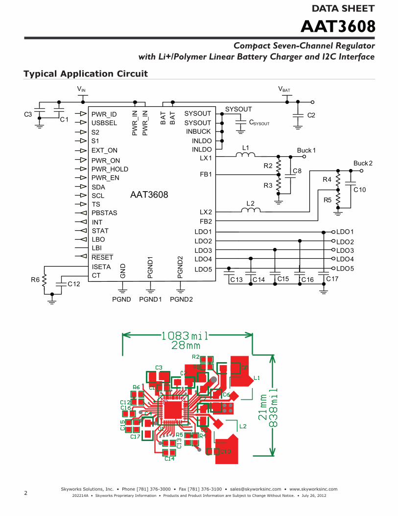
Typical Characteristics−LDO2 (continued)
Soft Start (VBAT = 3.6V; VLDO2 = 1.2V; ILDO2 = 80mA)
Time (100µs/div)
Enab
le V
olta
ge (t
op) (
V)LD
O2
Out
put V
olta
ge (m
iddl
e) (V
)
LDO
2 Output C
urrent(bottom
) (mA
)
0
1
2
3
4
0
50
100

AAT3608DATA SHEET
Compact Seven-Channel Regulatorwith Li+/Polymer Linear Battery Charger and I2C Interface
19Skyworks Solutions, Inc. • Phone [781] 376-3000 • Fax [781] 376-3100 • [email protected] • www.skyworksinc.com
202214A • Skyworks Proprietary Information • Products and Product Information are Subject to Change Without Notice. • July 26, 2012
Typical Characteristics−LDO3
System Line Transient Response(VIN = 3.5V to 5V; VBAT = 3.6V; VLDO3 = 1.2V; ILDO3 = 80mA; rising)
Time (200µs/div)
Syso
ut V
olta
ge (t
op) (
V)V B
AT V
olta
ge (m
iddl
e) (V
) LDO
3 Output Voltage
(bottom) (V)
3
4
5
6
1.0
1.1
1.2
1.3
1.4
System Line Transient Response(VIN = 3.5V to 5V; VBAT = 3.6V; VLDO3 = 1.2V; ILDO3 = 80mA; falling)
Time (200µs/div)
Syso
ut V
olta
ge (t
op) (
V)V B
AT V
olta
ge (m
iddl
e) (V
) LDO
3 Output Voltage
(bottom) (V)
3
4
5
6
1.0
1.1
1.2
1.3
Load Transient Response(ILDO3 = 8mA to 80mA; VBAT = 3.6V; CLDO3 = 4.7µF)
Time (200µs/div)
LDO
3 O
utpu
t Vol
tage
(bot
tom
) (V)
LDO
3 Output C
urrent(top) (m
A)
1.16
1.18
1.20
1.22
0
50
100
150
Line Regulation(VLDO3 = 1.2V)
VBAT Voltage (V)
LDO
3 O
utpu
t Acc
urac
y (%
)
3.8 4.0 4.23.2 3.4 3.6 4.4-0.3
-0.2
-0.1
0.0
0.1
0.2
0.3
IOUT = 0.1mAIOUT = 1mAIOUT = 10mAIOUT = 100mA
Output Voltage Error vs. Temperature(VBAT = 3.6V; VLDO3 = 1.2V)
Temperature (°C)
LDO
3 O
utpu
t Vol
tage
Err
or (%
)
-25 0-50 25 50 75 100-1.5
-1.0
-0.5
0.0
0.5
1.0
1.5
IOUT = 0.1mAIOUT = 1mAIOUT = 10mAIOUT = 100mA
Load Regulation(VBAT = 3.6V; VLDO3 = 1.2V)
Output Current (mA)
LDO
3 O
utpu
t Vol
tage
Err
or (%
)
1 100.1 100-1.5
-1.0
-0.5
0.0
0.5
1.0
1.5

AAT3608DATA SHEET
Compact Seven-Channel Regulatorwith Li+/Polymer Linear Battery Charger and I2C Interface
20Skyworks Solutions, Inc. • Phone [781] 376-3000 • Fax [781] 376-3100 • [email protected] • www.skyworksinc.com
202214A • Skyworks Proprietary Information • Products and Product Information are Subject to Change Without Notice. • July 26, 2012
Typical Characteristics−LDO3 (continued)
Soft Start (VBAT = 3.6V; VLDO3 = 1.2V; ILDO3 = 80mA)
Time (100µs/div)
Enab
le V
olta
ge (t
op) (
V)LD
O3
Out
put V
olta
ge (m
iddl
e) (V
)
LDO
3 Output C
urrent(bottom
) (mA
)
0
1
2
3
4
0
50
100

AAT3608DATA SHEET
Compact Seven-Channel Regulatorwith Li+/Polymer Linear Battery Charger and I2C Interface
21Skyworks Solutions, Inc. • Phone [781] 376-3000 • Fax [781] 376-3100 • [email protected] • www.skyworksinc.com
202214A • Skyworks Proprietary Information • Products and Product Information are Subject to Change Without Notice. • July 26, 2012
Typical Characteristics−LDO4
System Line Transient Response(VIN = 3.5V to 5V; VBAT = 3.6V; VLDO4 = 2.5V; ILDO4 = 50mA; rising)
Time (200µs/div)
Syso
ut V
olta
ge (t
op) (
V)V B
AT V
olta
ge (m
iddl
e) (V
) LDO
4 Output Voltage
(bottom) (V)
3
4
5
6
2.3
2.4
2.5
2.6
2.7
System Line Transient Response(VIN = 3.5V to 5V; VBAT = 3.6V; VLDO4 = 2.5V; ILDO4 = 50mA; falling)
Time (200µs/div)
Syso
ut V
olta
ge (t
op) (
V)V B
AT V
olta
ge (m
iddl
e) (V
) LDO
4 Output Voltage
(bottom) (V)
3
4
5
6
2.3
2.4
2.5
2.6
2.7
Load Transient Response(ILDO4 = 5mA to 50mA; VBAT = 3.6V; VLDO4 = 2.5V; CLDO4 = 4.7µF)
Time (200µs/div)
LDO
4 O
utpu
t Vol
tage
(bot
tom
) (V)
LDO
4 Output C
urrent(top) (A
)
2.46
2.48
2.50
2.52
0
50
100
150
Line Regulation(VLDO4 = 2.5V)
VBAT Voltage (V)
Out
put V
olta
ge E
rror
(%)
3.8 4.0 4.23.2 3.4 3.6 4.4-0.3
-0.2
-0.1
0.0
0.1
0.2
0.3
IOUT = 0.1mAIOUT = 1mAIOUT = 10mAIOUT = 100mA
Output Voltage Error vs. Temperature(VBAT = 3.6V; VLDO4 = 2.5V)
Temperature (°C)
LDO
4 O
utpu
t Vol
tage
Err
or (%
)
-25 0-50 25 50 75 100-1.5
-1.0
-0.5
0.0
0.5
1.0
1.5
IOUT = 0.1mAIOUT = 1mAIOUT = 10mAIOUT = 100mA
Load Regulation(VBAT = 3.6V; VLDO4 = 2.5V)
Output Current (mA)
LDO
4 O
utpu
t Vol
tage
Err
or (%
)
1 100.1 100-1.5
-1.0
-0.5
0.0
0.5
1.0
1.5

AAT3608DATA SHEET
Compact Seven-Channel Regulatorwith Li+/Polymer Linear Battery Charger and I2C Interface
22Skyworks Solutions, Inc. • Phone [781] 376-3000 • Fax [781] 376-3100 • [email protected] • www.skyworksinc.com
202214A • Skyworks Proprietary Information • Products and Product Information are Subject to Change Without Notice. • July 26, 2012
Typical Characteristics−LDO4 (continued)
Soft Start (VBAT = 3.6V; VLDO4 = 2.5V; ILDO4 = 50mA)
Time (100µs/div)
Enab
le V
olta
ge (t
op) (
V)LD
O4
Out
put V
olta
ge (m
iddl
e) (V
)
LDO
4 Output C
urrent(bottom
) (mA
)
0
1
2
3
4
0
50
100

AAT3608DATA SHEET
Compact Seven-Channel Regulatorwith Li+/Polymer Linear Battery Charger and I2C Interface
23Skyworks Solutions, Inc. • Phone [781] 376-3000 • Fax [781] 376-3100 • [email protected] • www.skyworksinc.com
202214A • Skyworks Proprietary Information • Products and Product Information are Subject to Change Without Notice. • July 26, 2012
Typical Characteristics−LDO5
System Line Transient Response(VIN = 3.5V to 5V; VBAT = 3.6V; VLDO5 = 3.3V; ILDO5 = 50mA; rising)
Time (200µs/div)
Syso
ut V
olta
ge (t
op) (
V)V B
AT V
olta
ge (m
iddl
e) (V
) LDO
5 Output Voltage
(bottom) (V)
3
4
5
6
3.1
3.2
3.3
3.4
3.5
System Line Transient Response(VIN = 3.5V to 5V; VBAT = 3.6V; VLDO5 = 3.3V; ILDO5 = 50mA; falling)
Time (200µs/div)
Syso
ut V
olta
ge (t
op) (
V)V B
AT V
olta
ge (m
iddl
e) (V
) LDO
5 Output Voltage
(bottom) (V)
3
4
5
6
3.1
3.2
3.3
3.4
3.5
Load Transient Response(ILDO5 = 5mA to 50mA; VBAT = 3.9V; CLDO5 = 4.7µF)
Time (200µs/div)
LDO
5 O
utpu
t Vol
tage
(bot
tom
) (V)
LDO
5 Output C
urrent(top) (A
)
3.26
3.28
3.30
3.32
3.34
0
50
100
150
Line Regulation(VLDO5 = 3.3V)
VBAT Voltage (V)
LDO
5 O
utpu
t Acc
urac
y (%
)
3.8 4.0 4.23.6 4.4-0.3
-0.2
-0.1
0.0
0.1
0.2
0.3
IOUT = 0.1mAIOUT = 1mAIOUT = 10mAIOUT = 100mA
Output Voltage Error vs. Temperature(VBAT = 3.6V; VLDO4 = 3.3V)
Temperature (°C)
LDO
5 O
utpu
t Vol
tage
Err
or (%
)
-25 0-50 25 50 75 100-1.5
-1.0
-0.5
0.0
0.5
1.0
1.5
IOUT = 0.1mAIOUT = 1mAIOUT = 10mAIOUT = 100mA
Load Regulation(VBAT = 3.6V; VLDO5 = 3.3V)
Output Current (mA)
LDO
5 O
utpu
t Vol
tage
Err
or (%
)
1 100.1 100-1.5
-1.0
-0.5
0.0
0.5
1.0
1.5

AAT3608DATA SHEET
Compact Seven-Channel Regulatorwith Li+/Polymer Linear Battery Charger and I2C Interface
24Skyworks Solutions, Inc. • Phone [781] 376-3000 • Fax [781] 376-3100 • [email protected] • www.skyworksinc.com
202214A • Skyworks Proprietary Information • Products and Product Information are Subject to Change Without Notice. • July 26, 2012
Typical Characteristics−LDO5 (continued)
Soft Start (VBAT = 3.6V; VLDO5 = 3.3V; ILDO5 = 50mA)
Time (100µs/div)
Enab
le V
olta
ge (t
op) (
V)LD
O5
Out
put V
olta
ge (m
iddl
e) (V
)
LDO
5 Output C
urrent(bottom
) (A)
0
1
2
3
4
0.00
0.05
0.10

AAT3608DATA SHEET
Compact Seven-Channel Regulatorwith Li+/Polymer Linear Battery Charger and I2C Interface
25Skyworks Solutions, Inc. • Phone [781] 376-3000 • Fax [781] 376-3100 • [email protected] • www.skyworksinc.com
202214A • Skyworks Proprietary Information • Products and Product Information are Subject to Change Without Notice. • July 26, 2012
Functional DescriptionThe AAT3608 is a complete power management solution. It seamlessly integrates a battery charger with two step-down converters and five low-dropout regulators to pro-vide power from either an external power source or a single-cell Lithium Ion/Polymer battery. Internal load switches allow the converters to operate from the best available power source.
If only the battery is available, then the voltage convert-ers are powered directly from the battery through a 100 mΩ load switch (BAT to SYSOUT). During this condition, the charger is put into sleep mode and draws less than 1µA quiescent current. If the system is connected to a wall adapter, then the voltage converters are powered directly from the adapter through a 200mΩ load-switch (PWR_IN to SYSOUT) and the battery is disconnected from the voltage converter inputs. This allows the sys-
tem to operate regardless of the state of the battery. It can even operate with no battery.
System Output (SYSOUT)Intelligent control of the integrated load switches is managed by the switch control circuitry. If the voltage across PWR_IN and GND pin is above the UVLO typical threshold voltage of 4.5, then the switch control will automatically short the load switch connecting PWR_IN to SYSOUT. Additionally, the charging switch will be enabled and switch connecting BAT and SYSOUT will be turned off. The location of the two switches and the bat-tery charging switch allows the step-down converter and LDO to always have the best available source of power. Furthermore, AAT3806 control logic allows the voltage converters to operate with no battery, or with a battery voltage below the trickle charge threshold.
Functional Block Diagram
Li-IonLinear
ChargerControl
Buck1
Reset
ThermalShutdown
EnableControl and
I2C Logic
LDO1 3.3V/3.0V/2.8 V (S1 & S2 bits)300mA max
LDO280mA max
LDO380mA max
LDO450mA max
INLDO
LX1
FB1
PGND1
1 Cell Li-Ion
SCLSDA
PWR_HOLD
EXT_ON
PWR_ON
Buck1 OK
LX2
FB2
PGND2
RESET
2µ
GND
L1
L2
INBUCK
Buck2
INBUCK
LDO2
LDO3
LDO4
LDO1
LDO550mA max
LDO5
INT
CT
ISETA
+
-+
BATLBO
LBI
LoadSwitch
SYSOUT BAT
STAT
To INBUCK, INLDO
PWR_EN
TS
2µ
1.0V
BAT
PBSTAS
BUCK1
320ms Debounce
320ms Debounce
S1 S2
USBSEL
BUCK1800mA max
BUCK2
FB2 is I2C adj.from 0.5V to 0.7V
800mA max
SYSOUT
PWR_ID
PWR_IN
1
2
3
40
37
38,39
4
12
14
32
34
33
30
31
15
16
17 19 18
11
10
7
5
8
6,9
20
21
22
23
13
27
26
25
2428,2935,36
ChargeSwitch
LBO
0.6V to 5.5V
Output is I2C adj.from 1.0 V to 1.4V
1.2V (default )
3.3V/2.85V/2.5V/1.8V (I2C)2.5V (default )
3.3V/3.0V/1.5V/1.2V (I2C)3.3V (default )
0.6V (default )
1.2 V (fixed)

AAT3608DATA SHEET
Compact Seven-Channel Regulatorwith Li+/Polymer Linear Battery Charger and I2C Interface
26Skyworks Solutions, Inc. • Phone [781] 376-3000 • Fax [781] 376-3100 • [email protected] • www.skyworksinc.com
202214A • Skyworks Proprietary Information • Products and Product Information are Subject to Change Without Notice. • July 26, 2012
Battery ChargingBattery charging commences only after the AAT3608 bat-tery charger checks several conditions in order to main-tain a safe charging environment. When an adapter input is connected to PWR_IN and is greater than 4.5V, the ENCHG bit is set (default) and the PWR_HOLD signal is high, the charger is enabled. The charger can be disabled by clearing the ENCHG bit through the I2C interface.
Figure 1 illustrates the entire battery charging profile or operation, which consists of three phases:
1. Preconditioning (Trickle) Charge2. Constant Current Charge3. Constant Voltage Charge
During battery charging, the battery charger initially checks the condition of the battery and determines which charging mode to apply. If the battery voltage is below VMIN, then the battery charger initiates trickle charge mode and charges the battery at 12% of the programmed constant-current magnitude. For example, if the pro-grammed current (ISETA) is 500mA, then the trickle charge current will be 60mA. Trickle charge is a safety precau-tion for a deeply discharged cell. It is intended to reduce stress on the battery, but also reduces the power dissipa-tion in the internal series pass MOSFET when the input-output voltage differential is at its highest.
Trickle charge continues until the battery voltage reach-es 2.8V. At this point the battery charger begins con-stant-current charging. The current level for this mode is programmed using a resistor from the ISETA pin to ground, or can be selected through the USBSEL pin with
settings of 100mA or 500mA; refer to the logic settings in Table 2. Constant-current charging continues until the voltage reaches the charge voltage regulation point.
VBAT_REG is factory programmed to 4.2V (nominal). Charging in constant-voltage mode will continue until the charge current has reduced to the charge termination current threshold. After the charge cycle is complete, the battery charger turns off the series pass device and automatically goes into a power saving sleep mode. During this time, the series pass device will block current in both directions to prevent the battery from discharg-ing through the battery charger.
The battery charger will remain in sleep mode even if the charger source is disconnected. It will come out of sleep mode when either the battery terminal voltage drops below the VRCH threshold, or the charging source is removed and reconnected. In all cases, the battery char-ger will monitor all parameters and resume charging in the most appropriate mode.
Battery Temperature Fault MonitoringThe TS pin is available to monitor the battery tempera-ture. Connect a 10k NTC resistor from the TS pin to ground. The TS pin outputs a 75µA constant current into the resistor and monitors the voltage to ensure that the battery temperature does not fall outside the operating limits depending on the temperature coefficient of the resistor used. When the voltage goes above 2.39V or goes below 0.331V, the charging will be suspended. A Beta range of 3300 to 4000 will place the typical charg-ing temperature between -4°C and 48°C.
Constant Current (CC)Charge Phase
PreconditioningTrickle Charge
PhaseCharge Complete Voltage
Constant Current ModeVoltage Threshold (VMIN)
Regulated Current
Trickle Charge andTermination Threshold
ICH_PRE
Battery Recharge Voltage Threshold
Battery DischargeConstant VoltageCharge Phase
Constant VoltageCharge Phase
(CC)
ICH_CC
Figure 1: Current vs. Voltage Profile During Charging Phases.

AAT3608DATA SHEET
Compact Seven-Channel Regulatorwith Li+/Polymer Linear Battery Charger and I2C Interface
27Skyworks Solutions, Inc. • Phone [781] 376-3000 • Fax [781] 376-3100 • [email protected] • www.skyworksinc.com
202214A • Skyworks Proprietary Information • Products and Product Information are Subject to Change Without Notice. • July 26, 2012
Battery Charging Flowchart
Power on Reset
Power Input Voltage
VIN > VUVLO
FaultConditions MonitoringOV, OT,
TS < VTS1 TS > VTS2
Preconditioning Trickle Charge
VBAT < VMIN
Constant CurrentVBAT < VBAT_EOC
Constant Voltage
IBAT > ITERM
No
No
Yes
No
Charge Completed
Charge Timer Control
No
Recharge Test VBAT < VRCH
Yes
No
Shut Down Yes
Enable
YesNo
Device Thermal Loop MonitorTJ > 115 C
Thermal LoopCurrent
Reduction in ADPCharging Mode
Thermal LoopCurrent
Reduction in C.C. Mode
No
Enable
Yes
Expired
No
Yes
Yes
Yes

AAT3608DATA SHEET
Compact Seven-Channel Regulatorwith Li+/Polymer Linear Battery Charger and I2C Interface
28Skyworks Solutions, Inc. • Phone [781] 376-3000 • Fax [781] 376-3100 • [email protected] • www.skyworksinc.com
202214A • Skyworks Proprietary Information • Products and Product Information are Subject to Change Without Notice. • July 26, 2012
Buck RegulatorsThe AAT3608 step-down converters are peak current mode PWM converters operating at 1.5MHz frequency. The input voltage range is 2.7V to 5.5V. The converters provide internal compensation. Power devices are sized for 800mA output current while maintaining over 85% efficiency at full load. Peak efficiency is above 90%. Light load efficiency is maintained at greater than 80% down to 85% of full load current. Soft start limits the current surge seen at the input and eliminates output voltage overshoot.
The input pin, INBUCK (Pin 24) must be connected to the SYSOUT output pin. The Buck1 output voltage is adjustable from 0.6V to 5.5V and is programmed through an external resistor divider. Buck2 output default value is set by external resistor feedback and then the feedback voltage can be dynamically adjusted via I2C in 12.5mV increments from 0.5V to 0.7V.
For overload conditions, the peak input current is limit-ed. Also, thermal protection completely disables switch-ing if internal dissipation becomes excessive, thus pro-tecting the device from damage. The junction over-temperature threshold is 140°C with 15°C of hysteresis. Under-voltage lockout (UVLO) guarantees sufficient VIN
bias and proper operation of all internal circuits prior to activation.
The current through the P-channel MOSFET (high side) is sensed for current loop control, as well as short circuit and overload protection. A fixed slope compensation signal is added to the sensed current to maintain stabil-ity for duty cycles greater than 50%. The peak current mode loop appears as a voltage-programmed current source in parallel with the output capacitor. The output of the voltage error amplifier programs the current mode loop for the necessary peak switch current to force a constant output voltage for all load and line conditions. Internal loop compensation terminates the transconduc-tance voltage error amplifier output. The reference volt-age is internally set to program the converter output voltage greater than or equal to 0.6V.
For conditions where the input voltage drops to the out-put voltage level, the converter duty cycle increases to 100%. As the converter approaches the 100% duty cycle, the minimum off-time initially forces the high side on-time to exceed the 1.5MHz clock cycle and reduces the effective switching frequency. Once the input drops
below the level where the converter can regulate the output, the high side P-channel MOSFET is enabled con-tinuously for 100% duty cycle. At 100% duty cycle the output voltage tracks the input voltage minus the I*R drop of the high side P-channel MOSFET.
For overload conditions, the peak input current is limit-ed. The bucks use a cycle-by-cycle current limit to pro-tect itself and the load from an external fault condition.Thermal protection completely disables switching when internal dissipation becomes excessive. The junction over-temperature threshold is 140°C with 15°C of hys-teresis. Once an over-temperature or over-current fault conditions is removed, the output voltage automatically recovers.
Low-Dropout RegulatorsThe advanced circuit design of the linear regulators has been specifically optimized for very fast start-up and shutdown timing. These proprietary LDOs are tailored for superior transient response characteristics. These traits are particularly important for applications which require fast power supply timing.
The high-speed turn-on capability is enabled through the implementation of a fast start control circuit, which accelerates the power up behavior of fundamental con-trol and feedback circuits within the LDO regulator. For fast turn-off time response is achieved by an active out-put pull down circuit, which is enabled when the LDO regulator is placed in the shutdown mode. This active fast shutdown circuit has no adverse effect on normal device operation.
There are two LDO input pins, INLDO (pins 6 and 9), which must be connected to the SYSOUT output pin.The LDO1 output voltage is selectable using pins S1 and S2 as shown in Table 1. LDO2 is fixed at 1.2V, LDO4 is fixed at 2.5V and LDO5 is fixed at 3.3V. LDO3 output default value is 1.2V and then can be dynamically adjusted via I2C in 25mV increments from 1.0V to 1.4V.
S1 S2 LDO10 0 3.0V0 1 3.3V1 0 2.8V1 1 Reserved
Table 1: LDO1 Output Voltages.

AAT3608DATA SHEET
Compact Seven-Channel Regulatorwith Li+/Polymer Linear Battery Charger and I2C Interface
29Skyworks Solutions, Inc. • Phone [781] 376-3000 • Fax [781] 376-3100 • [email protected] • www.skyworksinc.com
202214A • Skyworks Proprietary Information • Products and Product Information are Subject to Change Without Notice. • July 26, 2012
Controlling the System OutputsThe AAT3608 has a specific startup and shutdown condi-tions depending on its mode of operation.
Shutdown Mode“Shutdown Mode” is defined as the mode where the entire PMU (Power Management Unit) is shut down. This is a state that normally happens after all power has been disconnected from PWR_IN and BAT. Typically, after power has been applied and the part has been turned on, it will normally never need to be turned off. For GPS applications, the amount of time required for the SOC to start up from shutdown is prohibitively long, so the only time that it will go into Shutdown Mode (from any other mode) is when PWR_IN is disconnected and the BAT is below the Low-Battery comparator threshold.
Normal Mode“Normal Mode” is defined as the mode where all regula-tors are active. Once the part is in Normal Mode, it will typically go into Sleep or Deep-Sleep Mode when trying to save current.
SOC Sleep Mode“Sleep Mode” is an SOC-defined mode which simply means that all regulators are shut down except SYSOUT, Buck1, LDO1, and LDO3. To get into this mode from Normal, the SOC will pull the PWR_EN pin low to turn off LDO2, LDO4, and LDO5. Buck2 can also be controlled by PWR_EN only if the SOC masks PWR_EN through I2C.From a PMU point of view, it is no different from Normal Mode except for the regulators that have been switched off by pulling PWR_EN low.
Deep Sleep Mode“Deep Sleep Mode” is both an SOC and PMU-defined mode where all regulators have been turned off except for SYSOUT and Buck1. Data is backed up by the SOC and Buck1 stays alive to maintain the memory. LDO4 and LDO5 would be turned off separately by I2C, but the DS_RDY and PWR_DS I2C bits are used to get into and out of Deep Sleep Mode. See the flowchart diagrams for more detail.
PWR_ID PinThe PWR_ID pin is an input logic pin which determines the current limits and fast charge currents that will be used by PMU. PWR_ID settings are listed in Table 2.
Timing SequencesThe AAT3608 has a specific startup sequence when the device is activated. See the timing diagrams in Figures 2 through 7.
RESETThe RESET pin is an open drain active low output signal for system reset. Connect a pull-up resistor from the RESET pin to SYSOUT pin with a recommended resis-tance value of 100kΩ. After Buck2 and LDO2 reach their target nominal output voltage, a delay of 200ms exists before RESET goes high; refer to the timing diagram in Figure 2.
PWR_ID Pin USBSEL PinPWR_IN – SYSOUT
Switch Current Limit Battery Fast Charge CurrentL L 100mA (typical) 100mA (typical)L H 500mA (typical) 500mA (typical)H X Up to 1.2A (typical) Set by the resistor at the ISETA pin.
Table 2: PWR_ID Settings.

AAT3608DATA SHEET
Compact Seven-Channel Regulatorwith Li+/Polymer Linear Battery Charger and I2C Interface
30Skyworks Solutions, Inc. • Phone [781] 376-3000 • Fax [781] 376-3100 • [email protected] • www.skyworksinc.com
202214A • Skyworks Proprietary Information • Products and Product Information are Subject to Change Without Notice. • July 26, 2012
LDO4LDO5
LDO1BUCK1
RESET pin
PWR_EN pin
LDO2
BUCK2
SYSOUT SYSOUT
1ms 200ms
PWR_ EN disabled
Normal Mode Sleep ModePower on sequence
Power off sequence
LDO3
Normal Mode
PWR_ EN asserted
Wake up sequence
Triggered by PWR_EN
Figure 2: Normal Sleep Mode Sequence.
SOCAAT3608 PMU
GPIO
2u
320msDebounce
PBSTASPWR_ON
The PMU regulators only react to the PWR_EN pin.
X_PWR_EN
BUCK2 LDO2
LDO4 &LDO5
PWR_EN
The user pushes and releases the button to go into Sleep Mode.The user pushes and releases the pushbutton again to go back to Normal Mode.
PWR_HOLD
PWR_HOLD
Figure 3: Normal Sleep Mode Block Diagram.
AAT3608DATA SHEET
Compact Seven-Channel Regulatorwith Li+/Polymer Linear Battery Charger and I2C Interface
31Skyworks Solutions, Inc. • Phone [781] 376-3000 • Fax [781] 376-3100 • [email protected] • www.skyworksinc.com
202214A • Skyworks Proprietary Information • Products and Product Information are Subject to Change Without Notice. • July 26, 2012
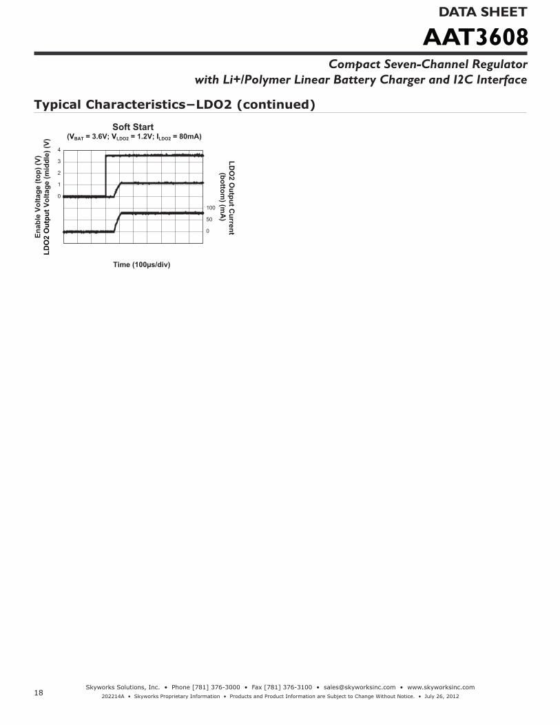
LDO5 (VDDA3V3_USB), LDO4 (VDDA2V5_USB, VDDIO_TSC,
VDDA_TSC, VREF_ADC)
T2
BUCK1
X_RESET_B
SYSOUT
T1
Normal Mode Deep-sleep ModePower on sequence
Power off sequence
Notes 1: T1 at least 650µS for internal LVR setup time; T2 is about 2ms to wait until PLL is stable; other time interval is dependent on power stability.Notes 2: After wake-up sequence from Deep-sleep Mode, the power on sequence to Normal Mode is similar to when powering on initially.
LDO3BUCK2
Normal Mode
Wake upsequence
LDO1LDO2
T2
LDO4LDO5
Figure 4: Normal Deep-Sleep Mode Sequence.
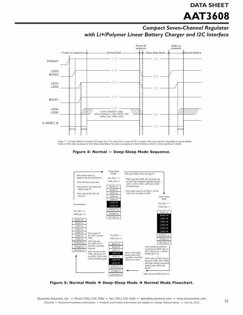
When Deep-Sleep is triggered (by the pushbutton)
-SOC will back up all data
-SOC will turn off LDO4 and LDO5 using I2C
-SOC will set DS_RDY bit using I2C
SOC sets PWR_DS bit through I2C.
PMU sees that PWR_DS has been set so then PMU disables regulators Buck2, LDO1, LDO2, LDO3, LDO4,and LDO5 simultaneously.
Each Buck output is at High-Z, but all LDOs will be pulled to GND.
Normal Mode
DS_RDY = 0PWR_DS = 0
Buck1 onBuck2 onLDO1 onLDO2 onLDO3 onLDO4 onLDO5 on
Charger on
LB comp on
Deep-Sleep Mode
DS_RDY = 1PWR_DS = 1
Buck2 offLDO1 offLDO2 offLDO3 offLDO4 offLDO5 off
Charger on
LB comp onSYSOUT on
SYSOUT on
Buck1 on
Deep-Sleep Ready
DS_RDY = 1PWR_DS = 0
Buck1 onBuck2 onLDO1 onLDO2 onLDO3 on
Charger on
LB comp on
SYSOUT on
LDO4 offLDO5 off
DS_RDY = 1PWR_DS = 0
Buck1 onBuck2 onLDO1 onLDO2 offLDO3 onLDO4 offLDO5 off
Charger on
LB comp on
SYSOUT on
User presses pushbutton connected to PWR_ON (or EXT_ON) pin for > 320ms (PWR_ON = H).
PMU looks at PWR_DS bit. Because PWR_DS=1,PMU will begin Startup sequence starting with LDO3 and Buck2.
PMU will force PWR_DS to 0.
SOC will pull up the PWR_EN pin to turn on LDO2, LDO4, and LDO5 simultaneously.
When LDO3 AND Buck2 reach 90% regulation, the PMU will turn on LDO1.
SOC reads I2CDS_RDY bit from PMU. SOC first sets DS_RDY bit to 0 and then retrieves memory.
Figure 5: Normal Mode Deep-Sleep Mode Normal Mode Flowchart.

AAT3608DATA SHEET
Compact Seven-Channel Regulatorwith Li+/Polymer Linear Battery Charger and I2C Interface
32Skyworks Solutions, Inc. • Phone [781] 376-3000 • Fax [781] 376-3100 • [email protected] • www.skyworksinc.com
202214A • Skyworks Proprietary Information • Products and Product Information are Subject to Change Without Notice. • July 26, 2012
Buck1 onBuck2 onLDO1 onLDO2 onLDO3 onLDO4 onLDO5 on
Charger on
LB comp on
SYSOUT on
Sleep Mode
Buck1 on
LDO1 on
LDO3 on
Charger on
LB comp on
SYSOUT on
LDO4 offLDO5 off
Buck2 off
LDO2 off
If a trigger event occurs, SOC pullsdown PWR_EN which turns off Buck2,
LDO2, LDO4, and LDO5 simultaneously.
Normal Mode
Buck1 onBuck2 onLDO1 onLDO2 onLDO3 onLDO4 onLDO5 on
Charger on
LB comp on
SYSOUT on
Buck1 on
LDO1 on
LDO3 on
Charger on
LB comp on
SYSOUT on
LDO4 offLDO5 off
Buck2 off
LDO2 off
If a trigger event occurs, PWR_ENis asserted to turn on Buck2, LDO2,
LDO4, and LDO5 simultaneously.
Figure 6: Normal Mode Sleep Mode Flowchart.
User presses pushbutton
connected toPWR_ON pin for >320ms.
(PWR_ON = H)
When LDO3 AND Buck2 reach 90%
regulation, PMU will turn onLDO1 and
Buck1
SOC will pull upPWR_EN pin toturn on LDO2,
LDO4, and LDO5 simultaneously.
RESET is pulled high
Normal Mode
DS_RDY = 0PWR_DS = 0
Buck1 onBuck2 onLDO1 onLDO2 onLDO3 onLDO4 onLDO5 on
Charger on
LB comp on
DS_RDY = 0PWR_DS = 0PWR_HOLD
is maintained high
Buck1 onBuck2 onLDO1 onLDO2 offLDO3 onLDO4 offLDO5 off
Charger on
LB comp on
Shutdown StartupDS_RDY = 0PWR_DS = 0
Buck1 offBuck2 offLDO1 offLDO2 offLDO3 offLDO4 offLDO5 off
Charger off
LB comp off
SYSOUT on
SYSOUT on
SYSOUT off
PMU begins Startup sequence starting with LDO3
and Buck2
If ADP and USB areremoved and the BATpin is < Low-Battery
threshold, the PMU will automatically go back into Shutdown mode.
All Regulators will beturned off simultaneously.
All bucks will be inHi-Z mode.
All LDOs will pulldown their outputs.
Figure 7: System Shutdown Normal Mode (Initial Start-Up) Flowchart.
AAT3608DATA SHEET
Compact Seven-Channel Regulatorwith Li+/Polymer Linear Battery Charger and I2C Interface
33Skyworks Solutions, Inc. • Phone [781] 376-3000 • Fax [781] 376-3100 • [email protected] • www.skyworksinc.com
202214A • Skyworks Proprietary Information • Products and Product Information are Subject to Change Without Notice. • July 26, 2012
I2C Serial Interface and Programmability
Serial InterfaceMany of the features of the AAT3608 can be controlled via the I2C serial interface. The I2C serial interface is a widely used interface where it requires a master to initi-ate all the communications with the slave devices. The I2C protocol consists of 2 active wires, SDA (serial data line) and SCL (serial clock line). Both wires are open drain and require an external pull up resistor to VCC
(SYSOUT may be used as VCC). The SDA pin serves I/O function, and the SCL pin controls and references the I2C bus. I2C protocol is a bidirectional bus which allows both read and write actions to take place. The timing diagram in Figure 8 depicts the transmission protocol.
START and STOP ConditionsSTART and STOP conditions are always generated by the master. Prior to initiating a START condition, both the SDA and SCL pin are idle mode (idle mode is when there is no activity on the bus and SDA and SCL are pulled to VCC via external resistor). As depicted in Figure 9, a START condi-tion is defined to be when the master pulls the SDA line low and after a short period pulls the SCL line low. A START condition acts as a signal to all ICs that something is about to be transmitted on the BUS. A STOP condition, also shown in Figure 9, is when the master releases the bus and SCL changes from low to high followed by SDA low to high transition. The master does not issue an ACKNOWLEDGE and releases the SCL and SDA pins.
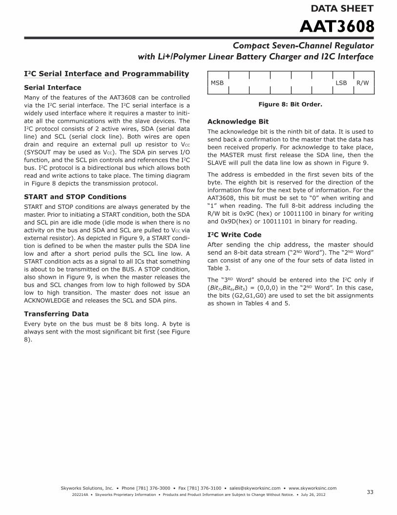
Transferring DataEvery byte on the bus must be 8 bits long. A byte is always sent with the most significant bit first (see Figure 8).
MSB LSB R/W
Figure 8: Bit Order.
Acknowledge BitThe acknowledge bit is the ninth bit of data. It is used to send back a confirmation to the master that the data has been received properly. For acknowledge to take place, the MASTER must first release the SDA line, then the SLAVE will pull the data line low as shown in Figure 9.
The address is embedded in the first seven bits of the byte. The eighth bit is reserved for the direction of the information flow for the next byte of information. For the AAT3608, this bit must be set to “0” when writing and “1” when reading. The full 8-bit address including the R/W bit is 0x9C (hex) or 10011100 in binary for writing and 0x9D(hex) or 10011101 in binary for reading.
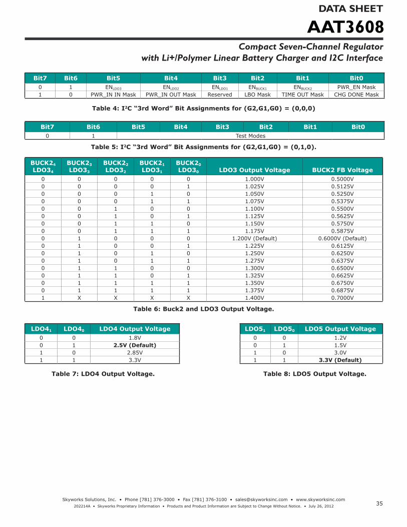
I2C Write CodeAfter sending the chip address, the master should send an 8-bit data stream (“2ND Word”). The “2ND Word” can consist of any one of the four sets of data listed in Table 3.
The “3RD Word” should be entered into the I2C only if (Bit7,Bit6,Bit5) = (0,0,0) in the “2ND Word”. In this case, the bits (G2,G1,G0) are used to set the bit assignments as shown in Tables 4 and 5.

AAT3608DATA SHEET
Compact Seven-Channel Regulatorwith Li+/Polymer Linear Battery Charger and I2C Interface
34Skyworks Solutions, Inc. • Phone [781] 376-3000 • Fax [781] 376-3100 • [email protected] • www.skyworksinc.com
202214A • Skyworks Proprietary Information • Products and Product Information are Subject to Change Without Notice. • July 26, 2012
A6 A5 A4 A3 A2 A1 0 0 0 0 x x G2 G1 G0
0 0 1 D14
0 1 0
0 1 1
D13 D12 D11 D10
D24 D23 D22 D21 D20
D34 D33 D32 D31 D30
0 1 E15 E14 E13 E12 E11 E10
1 0 E25 E24 E23 E22 E21 E20
1 1 E35 E34 E33 E32 E31 E30
0 1 F15 F14 F13 F12 F11 F10
G2:0=3'b000
G2:0=3'b010
I2C Address 2nd Word 3rd WordSTART STOP
STOP
STOP
STOP
SCL
SDA A6 A5 A0 W A
0
Write command from the master.
Acknowledge from the slave.
R/W
START
0
STOP
Dx4 Dx0
STOP
A
Acknowledge from the slave.
START command from the master.
STOP command from the master.
SCL
SDA
D1<4:0>
D2<4:0>
D3<4:0>
E1<5:0>
E2<5:0>
E3<5:0>
F1<5:0>
I2C Controller
01 or 10 or 11
72819
A<6:0>
Data Data Data Data
ACK ACK ACK
Figure 9: I2C Protocol.
Bit7 Bit6 Bit5 Bit4 Bit3 Bit2 Bit1 Bit00 0 0 0 0 G2 G1 G00 0 1 ENLDO5 ENLDO4 DS_RDY PWR_DS Reserved0 1 0 LDO51 LDO50 LDO41 LDO40 ENCHG
0 1 1 BUCK24 and LDO34 BUCK23 and LDO33 BUCK22 and LDO32 BUCK21 and LDO31 BUCK20 and LDO30
Table 3: I2C “2nd Word” Bit Assignments.
AAT3608DATA SHEET
Compact Seven-Channel Regulatorwith Li+/Polymer Linear Battery Charger and I2C Interface
35Skyworks Solutions, Inc. • Phone [781] 376-3000 • Fax [781] 376-3100 • [email protected] • www.skyworksinc.com
202214A • Skyworks Proprietary Information • Products and Product Information are Subject to Change Without Notice. • July 26, 2012
Bit7 Bit6 Bit5 Bit4 Bit3 Bit2 Bit1 Bit00 1 ENLDO3 ENLDO2 ENLDO1 ENBUCK1 ENBUCK2 PWR_EN Mask1 0 PWR_IN IN Mask PWR_IN OUT Mask Reserved LBO Mask TIME OUT Mask CHG DONE Mask
Table 4: I2C “3rd Word” Bit Assignments for (G2,G1,G0) = (0,0,0)
Bit7 Bit6 Bit5 Bit4 Bit3 Bit2 Bit1 Bit00 1 Test Modes
Table 5: I2C “3rd Word” Bit Assignments for (G2,G1,G0) = (0,1,0).
BUCK24
LDO34
BUCK23
LDO33
BUCK22
LDO32
BUCK21
LDO31
BUCK20
LDO30 LDO3 Output Voltage BUCK2 FB Voltage0 0 0 0 0 1.000V 0.5000V0 0 0 0 1 1.025V 0.5125V0 0 0 1 0 1.050V 0.5250V0 0 0 1 1 1.075V 0.5375V0 0 1 0 0 1.100V 0.5500V0 0 1 0 1 1.125V 0.5625V0 0 1 1 0 1.150V 0.5750V0 0 1 1 1 1.175V 0.5875V0 1 0 0 0 1.200V (Default) 0.6000V (Default)0 1 0 0 1 1.225V 0.6125V0 1 0 1 0 1.250V 0.6250V0 1 0 1 1 1.275V 0.6375V0 1 1 0 0 1.300V 0.6500V0 1 1 0 1 1.325V 0.6625V0 1 1 1 1 1.350V 0.6750V0 1 1 1 1 1.375V 0.6875V1 X X X X 1.400V 0.7000V
Table 6: Buck2 and LDO3 Output Voltage.
LDO41 LDO40 LDO4 Output Voltage LDO51 LDO50 LDO5 Output Voltage0 0 1.8V 0 0 1.2V0 1 2.5V (Default) 0 1 1.5V1 0 2.85V 1 0 3.0V1 1 3.3V 1 1 3.3V (Default)
Table 7: LDO4 Output Voltage. Table 8: LDO5 Output Voltage.

AAT3608DATA SHEET
Compact Seven-Channel Regulatorwith Li+/Polymer Linear Battery Charger and I2C Interface
36Skyworks Solutions, Inc. • Phone [781] 376-3000 • Fax [781] 376-3100 • [email protected] • www.skyworksinc.com
202214A • Skyworks Proprietary Information • Products and Product Information are Subject to Change Without Notice. • July 26, 2012
Interrupt (Read from I2C)A single byte is used when reading I2C data from the AAT3608. The R/W address should be set to 1 so that complete address of the chip would be 0x9D or 10011101 in binary.
The INT (interrupt) pin is an open drain output which pulls low when there is an assertion in any one of the status bits (except the DS_RDY and PWR_DS bits). When a Read from the I2C is initiated AND completed by the SOC, the INT pin is released and the voltage will go high through the external pull-up resistor.
ENCHG Description DS_RDY Description0 Turn off Battery Charger 0 (Default)1 Turn on Battery Charger (Default) 1 Deep Sleep Recognition Flag
ENBUCK1 Description PWR_DS Description0 Turn off Buck1 0 (Default)1 Turn on Buck1 (Default) 1 Force PMU to go into Deep Sleep Mode
ENBUCK2 Description PWR_EN Mask Description0 Turn OFF Buck2 0 No Masking1 Turn ON Buck2 (Default) 1 Mask the PWR_EN pin ability to control BUCK2 (Default)
ENLDO1 Description PWR_IN IN Mask Description0 Turn OFF LDO1 0 No Masking
1 Turn ON LDO1 (Default) 1 Prevent an interrupt from being generated if the PWR_IN IN bit has been asserted (Default)
ENLDO2 Description PWR_IN OUT Mask Description0 Turn OFF LDO2 0 No Masking
1 Turn ON LDO2 only if PWR_EN pin is High (Default) 1 Prevent an interrupt from being generated if the
PWR_IN OUT bit has been asserted (Default)ENLDO3 Description LBO Mask Description
0 Turn OFF LDO3 0 No Masking
1 Turn ON LDO3 (Default) 1 Prevent an interrupt from being generated if the LBO comparator has been asserted (Default)
ENLDO4 Description TIMEOUT Mask Description0 Turn OFF LDO4 0 No Masking
1 Turn ON LDO4 (Default) 1 Prevents an interrupt from being generated if the TIMEOUT bit has been asserted (Default)
ENLDO5 Description CHG_DONE Mask Description0 Turn OFF LDO5 0 No Masking
1 Turn ON LDO5 (Default) 1 Prevent an interrupt from being generated if the charger has reached End-of-Charge (Default)
Table 9: Enable Settings.
Bit7 Bit6 Bit5 Bit4 Bit3 Bit2 Bit1 Bit0PWR_IN IN PWR_IN OUT Reserved LBO TIME OUT CHG_DONE DS_RDY PWR_DS
Table 10: I2C Read Table.

AAT3608DATA SHEET
Compact Seven-Channel Regulatorwith Li+/Polymer Linear Battery Charger and I2C Interface
37Skyworks Solutions, Inc. • Phone [781] 376-3000 • Fax [781] 376-3100 • [email protected] • www.skyworksinc.com
202214A • Skyworks Proprietary Information • Products and Product Information are Subject to Change Without Notice. • July 26, 2012
PWR_IN IN Bit DescriptionInterrupt Signal
Produced?0 Default Only if PWR_IN IN Mask
bit is not set1 If VPWR_IN > UVLO threshold, this bit will be set
PWR_IN OUT Bit DescriptionInterrupt Signal
Produced?0 Default Only if PWR_IN OUT
Mask bit is not set1 If VPWR_IN < UVLO threshold, this bit will be set
TIMEOUT Bit DescriptionInterrupt Signal
Produced?0 Default Only if TIMEOUT Mask
bit is not set1 If the charger watchdog timer has reached Timeout, this bit will be set.
LBO Bit DescriptionInterrupt Signal
Produced?0 Default Only if LBO Mask bit is
not set1 If Low-Battery comparator is tripped then this bit will be set.
CHG DONE Bit DescriptionInterrupt Signal
Produced?0 Default Only if CHG_DONE
Mask bit is not set1 If the Charger has reached End-Of-Charge (EOC), this bit will be set
DS_RDY Bit DescriptionInterrupt Signal
Produced?0 Default
No INT signal1 Same as the DS_RDY bit described in the "I2C Write" section of this datasheet
PWR_DS Bit DescriptionInterrupt Signal
Produced?0 Default
No INT signal1 Same as the PWR_DS bit described in the "I2C Write" section of this datasheet
Table 11: Status Bit Descriptions.

AAT3608DATA SHEET
Compact Seven-Channel Regulatorwith Li+/Polymer Linear Battery Charger and I2C Interface
38Skyworks Solutions, Inc. • Phone [781] 376-3000 • Fax [781] 376-3100 • [email protected] • www.skyworksinc.com
202214A • Skyworks Proprietary Information • Products and Product Information are Subject to Change Without Notice. • July 26, 2012
Application InformationThe two bucks are high performance 800mA 1.5MHz monolithic step-down converters. They have been designed with the goal of minimizing external compo-nent size and optimizing efficiency over the complete load range. Apart from the small bypass input capacitor, only a small L-C filter is required at the output.
Both bucks can be programmed with external feedback resistors to any voltage, ranging from 0.6V to the input voltage in default feedback voltage condition.
At dropout, the step down converters duty cycle increas-es to 100% and the output voltage tracks the input volt-age minus the RDSON drop of the P-channel high-side MOSFET.
Output Voltage Resistor SelectionResistors R2 through R5 in Figure 10 program the output to regulate at a voltage higher than 0.6V in default mode. The feedback voltage of Buck2 can have a wider range and can be adjusted down to 0.5V through I2C. To limit the bias current required for the external feedback resistor string while maintaining good noise immunity, a suggested value for R3 and R5 is 59kΩ to provide a bias current of 10uA with a feedback voltage of 0.6V. Although a larger value will further reduce quiescent current, it will also increase the impedance of the feed-back node, making it more sensitive to external noise and interference. Table 12 summarizes the resistor val-ues for various output voltages with R3 and R5 set to either 59kΩ for good noise immunity or 100kΩ for reduced no load input current.
VOUT (V)
R3 and R5 = 59kΩR2 and R4 (kΩ)
R3 and R5 = 100kΩR2 and R4 (kΩ)
0.8 19.6 33.20.9 29.4 49.91 39.2 66.5
1.1 49.9 82.51.2 59 1001.3 68.1 1181.4 78.7 1331.5 88.7 1501.8 118 2001.85 124 210
2 137 2322.5 187 3163.3 267 453
Table 12: Feedback Resistors (Feedback Voltage = 0.6V).
Input Capacitor (Bucks)All input capacitors should be located as physically close to the power pin (INBUCK) and power ground pins (PGND1 and 2). Ceramic capacitors are recommended for their higher current operation and small profile. Also, ceramic capacitors are inherently capable to withstand input current surges from low impedance sources such as batteries in portable devices over tantalum capacitors. Typically, 10V or 16V rated capacitors are required.
The following are the typical recommended capacitance values:
Two 10μF capacitors for INBUCKOne 10μF capacitor for INLDOOne 10μF capacitor for SYSOUTOne 10μF capacitor for PWR_INOne 10μF capacitor for BAT
Output Capacitor (Bucks)For proper load voltage regulation and operational stabil-ity, a capacitor is required on the output of each buck. The output capacitor connection to the ground pin should be made as directly as practically possible for maximum device performance. Since the bucks have been designed to function with very low ESR capacitors, a 4.7μF ceramic capacitor is recommended for best per-formance.
Inductor SelectionThe two bucks use peak current mode control with slope compensation to maintain stability for duty cycles great-er than 50%. The output inductor value must be select-ed so the inductor current down slope meets the internal slope compensation requirements. The internal slope compensation is 1A/μs. The inductor should be set equal to the output voltage numeric value in micro henries (μH). This guarantees that there is sufficient internal slope compensation.
Inductor manufacturer’s specifications list both the inductor DC current rating, which is a thermal limitation, and the peak current rating, which is determined by the saturation characteristics. The inductor should not show any appreciable saturation under normal load condi-tions. Some inductors may meet the peak and average current ratings yet result in excessive losses due to a high DCR. Always consider the losses associated with the DCR and its effect on the total converter efficiency when selecting an inductor.

AAT3608DATA SHEET
Compact Seven-Channel Regulatorwith Li+/Polymer Linear Battery Charger and I2C Interface
39Skyworks Solutions, Inc. • Phone [781] 376-3000 • Fax [781] 376-3100 • [email protected] • www.skyworksinc.com
202214A • Skyworks Proprietary Information • Products and Product Information are Subject to Change Without Notice. • July 26, 2012
Input Capacitor (LDOs)Typically, a 10μF or larger capacitor, C4 (see Figure 10), is recommended as close as possible to the device INLDO pin. The input capacitor value of 10μF will offer superior input line transient response and will assist in maximizing the highest possible power supply ripple rejection.
There is no specific capacitor ESR requirement; there-fore ceramic, tantalum, or aluminum electrolytic capaci-tors may be selected for capacitor C4. However, ceramic capacitors are recommended due to their inherent capa-bility over tantalum capacitors to withstand input cur-rent surges from low impedance sources such as batter-ies in portable devices.
Output Capacitor (LDOs)For proper load voltage regulation and operational sta-bility, a 4.7µF ceramic capacitor is required between the output of the LDOs and GND. If desired, the output capacitor may be increased without limit. The output capacitor connection to the LDO regulator ground pin should be made as direct as practically possible for maximum device performance.
Although the device is intended to operate with low ESR capacitors, it is stable over a very wide range of capaci-tor ESR, thus it will also work with higher ESR tantalum or aluminum electrolytic capacitors. However, for best performance, ceramic capacitors are recommended.
Layout GuidanceFigure 10 is the schematic for the evaluation board. The evaluation board has extra components for easy evalua-tion; the bill of materials for the system is shown in Table 12. When laying out the PC board, the following layout guidelines should be followed to ensure proper operation of the AAT3608:
1. The exposed pad (EP) must be reliably soldered to exposed copper pad on the board and electrically connected to GND/PGND pins.
2. The power traces, including GND traces, the LX traces and the VIN trace should be kept short, direct and wide to allow large current flow. Use several via pads when routing between layers.
3. The input capacitors should be connected as close as possible from SYSOUT and INBUCK to PGND1 and PGND2 to get good power filtering.
4. Keep the switching node LX away from the sensitive buck feedback nodes, FB1 and FB2.
5. The feedback trace for the bucks should be separate from any power trace and connected as closely as possible to the load point. Sensing along a high cur-rent load trace will degrade DC load regulation.
6. The output capacitors and inductors should be con-nected as close as possible and there should not be any signal lines under the inductor.
7. The resistance of the trace from the load return to PGND1 and PGND2 should be kept to a minimum. This will help to minimize any error in DC regulation due to differences in the potential of the internal signal ground and the power ground.

AAT3608DATA SHEET
Compact Seven-Channel Regulatorwith Li+/Polymer Linear Battery Charger and I2C Interface
40Skyworks Solutions, Inc. • Phone [781] 376-3000 • Fax [781] 376-3100 • [email protected] • www.skyworksinc.com
202214A • Skyworks Proprietary Information • Products and Product Information are Subject to Change Without Notice. • July 26, 2012
J2J1
J4SYSOUT
SYSOUT
J8J9
J10
J11J12
LDO1LDO1
LDO2
LDO3
LDO4
LDO5
LDO2
LDO3
LDO4LDO5
C134.7µF
C144.7µF
C120.1µF
C1 0.1µF
C3 10µF
C2 10µF
C9100pF
C154.7µF
C164.7µF
C174.7µF
C104.7µF
C84.7µF
RESETRESET
J6
J27 Buck 2
J3Buck 1
BUCK2
BUCK1
P35,36
xRESET
RESET
L2 2.2µH
L1 2.2µH
PWR_IDUSBSEL
STAT
STAT
PBSTAS
PBSTAS
VBAT
VBAT
VBATVBAT
BATBAT
VIN
VINVIN
PWR_ONSW1
PWR_ON
J5
SCL
SYSOUT
SYSOUTSYSOUTSYSOUT
SYSOUT
VBAT
R1710K
R1210K
R21100K
R4100K
R3100K
R2316K
R5100K
R201M
R152M
R161M
R14100K
R61.24K
R191.5K
R1310K
R1810K
LBI
LBI
LBO
LBO
S2S1
1M 1M 1M 1M 1M
R7 R8
INTINT
PWR_EN
12
TB1
TB-2
TB2
TB-2
12
123456
121110987
S1
SW DIP-6
SYSOUT
D1
LED2
R9 R10 R11
12
3
J17
J18
J19
J13
J21J20
J16
J15
J14
12
12
TB4
TB-2
TB3
TB-2
FB = 0.6V
12
3
J7
3-PIN_JUMPER
SYSOUT
VBAT
VBAT
TSTS
STAT1
ISETA2
TS3
TC4
17 26 22
LDO2 5
6
LDO3 7
LDO1 8
INLDOINLDO
9
LDO4 10
LDO5 11
PBSTAS12
13
INT14
LBO15
LBI16
S218
S119
PWR_EN20
21
23
INBUCK 24
LX1 25
FB1
LX2
FB2
27SDA30
SCL31
PWR_HOLD32PWR_ON33EXT_ON34
35SYSOUTSYSOUT
3
39 38 29 28
6PWR_IDPWR_INPWR_IN37
USBSEL
STAT
TS
PBSTAS
INT
LBO
LBI
S2S1
PWR_EN
SDASCL
PWR_HOLDPWR_ONEXT_ONEXT_ON
PWR_IDUSBSEL 40
U1 AAT3608
12
3
3-PIN_JUMPER
BUCK1
PWR_HOLD
P24P24
C4 10µF
C5 10µF
C610µF
C710µF
P6,9
Star Ground is the Exposed Pad: Connect all Ground Planes at the Exposed Pad
C19100pF
C18100pF
1 23 45 67 89 10
P1
Header 5X2
SDAVIO
PGND
PGND
PGND
PGND
PGNDPGND
PGND
GND
GND GND GND
PGND
PGND
PGNDPGND
GND PGND1
PGND1
PGND2
PGND2
PGND
PGND
PGNDPGND1PGND2PGND
GND
GND
PGND2
PGND1
PGNDPGND PGND
PGND
J23
J22
J25 J24 J28 J29 LX2
J26LX1
Figure 10: AAT3608 Evaluation Board Schematic.

AAT3608DATA SHEET
Compact Seven-Channel Regulatorwith Li+/Polymer Linear Battery Charger and I2C Interface
41Skyworks Solutions, Inc. • Phone [781] 376-3000 • Fax [781] 376-3100 • [email protected] • www.skyworksinc.com
202214A • Skyworks Proprietary Information • Products and Product Information are Subject to Change Without Notice. • July 26, 2012
Figure 11: AAT3608 Evaluation Board Silk Screen Layer.
Figure 12: AAT3608 Evaluation Board Top Layer. Figure 13: AAT3608 Evaluation Board
Mid Layer 1 (GND Plane).

AAT3608DATA SHEET
Compact Seven-Channel Regulatorwith Li+/Polymer Linear Battery Charger and I2C Interface
42Skyworks Solutions, Inc. • Phone [781] 376-3000 • Fax [781] 376-3100 • [email protected] • www.skyworksinc.com
202214A • Skyworks Proprietary Information • Products and Product Information are Subject to Change Without Notice. • July 26, 2012
Figure 14: AAT3608 Evaluation Board Figure 15: AAT3608 Evaluation Board
Mid Layer 2 (SYSOUT). Bottom Layer.
Description Value Quantity FootprintU1 Battery Charger PMU 1 TQFN55-40L
J1, J2, J3, J4, J5, J6, J8, J9, J10, J11, J12, 13, J14,J15, J16,
J18, J20, J21, J22, J23, J24, J25, J26, J27, J28, J29
Test Point 26 TP
TB1, TB2, TB3, TB4 Terminal Block Connector 2 Positions - DigiKey 277-1273-ND 4 TBLOK2
SW1 Switch Tact, SPST, 5mm - C&K Components PTS645TL50 LFS 1 SW-2
P1 Header, 5-Pin, Dual row 1 HDR2X5J7, J17, J19 1X3 Header 3 HDR1X3
S1 DIP Switch, 6 Position, SPST 1 DIP-12/SWL1, L2 Inductor 2.2µH 2 CDRH4D16
D1 Typical red, green, yellow, amber GaAs LED 1 1206LED - duplicateC2, C3, C4, C5,C6,C7 Ceramic Capacitor 10µF 6 0805
C8 Ceramic Capacitor 4.7µF 1 0805C1, C12 Ceramic Capacitor 0.1µF 2 0603
C10, C13, C14, C15, C16, C17 Ceramic Capacitor 4.7µF 6 0603C9, C18, C19 Ceramic Capacitor 100pF 3 0603
R12, R13, R17, R18 Resistor 10K 4 0603R15 Resistor 2M 1 0603R19 Resistor 1.5K 1 0603R2 Resistor 316K 1 0603
R3, R4, R5, R14, R21 Resistor 100K 5 0603R6 Resistor 1.24K 1 0603
R7, R8, R9, R10, R11, R16, R20 Resistor 1M 7 0603
Table 12: AAT3608 Evaluation Board Bill of Materials (BOM).

AAT3608DATA SHEET
Compact Seven-Channel Regulatorwith Li+/Polymer Linear Battery Charger and I2C Interface
43Skyworks Solutions, Inc. • Phone [781] 376-3000 • Fax [781] 376-3100 • [email protected] • www.skyworksinc.com
202214A • Skyworks Proprietary Information • Products and Product Information are Subject to Change Without Notice. • July 26, 2012
1. XYY = assembly and date code.2. Sample stock is generally held on part numbers listed in BOLD.3. Available exclusively outside of the United States and its territories.4. The leadless package family, which includes QFN, TQFN, DFN, TDFN and STDFN, has exposed copper (unplated) at the end of the lead terminals due to the manufacturing
process. A solder fillet at the exposed copper edge cannot be guaranteed and is not required to ensure a proper bottom solder connection.
Ordering Information
Package Marking1 Part Number (Tape and Reel)2, 3
TQFN55-40 C8XYY AAT3608IIC-1-T1
Skyworks Green™ products are compliant with all applicable legislation and are halogen-free.For additional information, refer to Skyworks Definition of Green™, document number SQ04-0074.
Package Information
TQFN55-404
Top View
Side View
Bottom View
5.000 ± 0.050
5.00
0 ±
0.05
0
Pin 1 Dotby Marking
Pin 1 IdentificationChamfer 0.300 x 45°
3.600 ± 0.050
3.60
0 ±
0.05
0
0.450 ± 0.050
0.380 ± 0.050
0.20
0 ±
0.05
00.
400
BS
C
0.750 ± 0.050
0.000 + 0.100- 0.000
0.203 REF
All dimensions in millimeters.

AAT3608DATA SHEET
Compact Seven-Channel Regulatorwith Li+/Polymer Linear Battery Charger and I2C Interface
44Skyworks Solutions, Inc. • Phone [781] 376-3000 • Fax [781] 376-3100 • [email protected] • www.skyworksinc.com
202214A • Skyworks Proprietary Information • Products and Product Information are Subject to Change Without Notice. • July 26, 2012
Copyright © 2012 Skyworks Solutions, Inc. All Rights Reserved.
Information in this document is provided in connection with Skyworks Solutions, Inc. (“Skyworks”) products or services. These materials, including the information contained herein, are provided by Skyworks as a service to its customers and may be used for informational purposes only by the customer. Skyworks assumes no responsibility for errors or omissions in these materials or the information contained herein. Sky-works may change its documentation, products, services, specifications or product descriptions at any time, without notice. Skyworks makes no commitment to update the materials or information and shall have no responsibility whatsoever for conflicts, incompatibilities, or other difficulties arising from any future changes.
No license, whether express, implied, by estoppel or otherwise, is granted to any intellectual property rights by this document. Skyworks assumes no liability for any materials, products or information provided here-under, including the sale, distribution, reproduction or use of Skyworks products, information or materials, except as may be provided in Skyworks Terms and Conditions of Sale.
THE MATERIALS, PRODUCTS AND INFORMATION ARE PROVIDED “AS IS” WITHOUT WARRANTY OF ANY KIND, WHETHER EXPRESS, IMPLIED, STATUTORY, OR OTHERWISE, INCLUDING FITNESS FOR A PARTICULAR PURPOSE OR USE, MERCHANTABILITY, PERFORMANCE, QUALITY OR NON-INFRINGEMENT OF ANY INTELLECTUAL PROPERTY RIGHT; ALL SUCH WARRANTIES ARE HEREBY EXPRESSLY DISCLAIMED. SKYWORKS DOES NOT WARRANT THE ACCURACY OR COMPLETENESS OF THE INFORMATION, TEXT, GRAPHICS OR OTHER ITEMS CONTAINED WITHIN THESE MATERIALS. SKYWORKS SHALL NOT BE LIABLE FOR ANY DAMAGES, IN-CLUDING BUT NOT LIMITED TO ANY SPECIAL, INDIRECT, INCIDENTAL, STATUTORY, OR CONSEQUENTIAL DAMAGES, INCLUDING WITHOUT LIMITATION, LOST REVENUES OR LOST PROFITS THAT MAY RESULT FROM THE USE OF THE MATERIALS OR INFORMATION, WHETHER OR NOT THE RECIPIENT OF MATERIALS HAS BEEN ADVISED OF THE POSSIBILITY OF SUCH DAMAGE.
Skyworks products are not intended for use in medical, lifesaving or life-sustaining applications, or other equipment in which the failure of the Skyworks products could lead to personal injury, death, physical or en-vironmental damage. Skyworks customers using or selling Skyworks products for use in such applications do so at their own risk and agree to fully indemnify Skyworks for any damages resulting from such improper use or sale.
Customers are responsible for their products and applications using Skyworks products, which may deviate from published specifications as a result of design defects, errors, or operation of products outside of pub-lished parameters or design specifications. Customers should include design and operating safeguards to minimize these and other risks. Skyworks assumes no liability for applications assistance, customer product design, or damage to any equipment resulting from the use of Skyworks products outside of stated published specifications or parameters.
Skyworks, the Skyworks symbol, and “Breakthrough Simplicity” are trademarks or registered trademarks of Skyworks Solutions, Inc., in the United States and other countries. Third-party brands and names are for identification purposes only, and are the property of their respective owners. Additional information, including relevant terms and conditions, posted at www.skyworksinc.com, are incorporated by reference.