
D3.6 V 3 1 - UPC Universitat Politècnica de...
98
TRAMS project, FP7INFSOIST248789 page 1/98 1. Executive Summary This document, deliverable D3.6, presents the results of the work performed in Work Package 3 (WP3) on the analysis of the effect of environmental (V, voltage fluctuations, T, temperature and SEU, single even upsets) as well as process parameter (P) and degradation mechanisms on the performance variability of the memories at cell and system levels. This deliverable at circuit and system level completes Milestone MS2 (M12) together with deliverable D1.1 at device level. The title of MS2 is “Variability and Reliability analysis for bulk CMOS”. The work is entirely inside Task 3.1; the analysis of the impact of PVT variations is a required precedent to the task of mitigation techniques (T3.1) and countermeasure techniques (T3.2) corresponding to the second year work (milestones 4, 7 and 8), see Figure 1. Both, static and dynamic memory cells and circuits, have been contemplated in this work, considering as key cells the 6T for SRAM [1] and the 3T1D [2] (and partially 1T1C [3]) for DRAM. To evaluate the impact of the PVT variations, Hspice tool has been used. The MOS models taken into account have been the Si bulk CMOS for 45, 32, 22 and 16 nm nodes (Predictive Technology Models [4], PTM) with specific variability scenario described in section 3.2, and the 18 and 13 nm technologies result of WP1 (models specific of the TRAMS project). Due to the fact that Tasks 1.1 and 1.2 already work with the Carbon Nanotube Field Effect Transistor Technology Variability analysis as main objective (with the use of the CNTFET Hspice model from Stanford [5]) a section to compare the impact of PVT in Silicon technology and CNTFET has been included in this document (the comparison is concentrated only on the 6T cell) in Section 8. Figure 1. Organization of Work Package 3 (WP3)
Transcript of D3.6 V 3 1 - UPC Universitat Politècnica de...

TRAMS project, FP7-‐INFSO-‐IST-‐248789
page 1/98
1. Executive Summary This document, deliverable D3.6, presents the results of the work performed in Work Package 3 (WP3) on the analysis of the effect of environmental (V, voltage fluctuations, T, temperature and SEU, single even upsets) as well as process parameter (P) and degradation mechanisms on the performance variability of the memories at cell and system levels. This deliverable at circuit and system level completes Milestone MS2 (M12) together with deliverable D1.1 at device level. The title of MS2 is “Variability and Reliability analysis for bulk CMOS”. The work is entirely inside Task 3.1; the analysis of the impact of PVT variations is a required precedent to the task of mitigation techniques (T3.1) and countermeasure techniques (T3.2) corresponding to the second year work (milestones 4, 7 and 8), see Figure 1.
Both, static and dynamic memory cells and circuits, have been contemplated in this work, considering as key cells the 6T for SRAM [1] and the 3T1D [2] (and partially 1T1C [3]) for DRAM. To evaluate the impact of the PVT variations, Hspice tool has been used. The MOS models taken into account have been the Si bulk CMOS for 45, 32, 22 and 16 nm nodes (Predictive Technology Models [4], PTM) with specific variability scenario described in section 3.2, and the 18 and 13 nm technologies result of WP1 (models specific of the TRAMS project). Due to the fact that Tasks 1.1 and 1.2 already work with the Carbon Nanotube Field Effect Transistor Technology Variability analysis as main objective (with the use of the CNTFET Hspice model from Stanford [5]) a section to compare the impact of PVT in Silicon technology and CNTFET has been included in this document (the comparison is concentrated only on the 6T cell) in Section 8.
Figure 1. Organization of Work Package 3 (WP3)
TRAMS project, FP7-‐INFSO-‐IST-‐248789
page 2/98
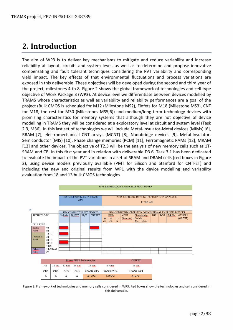
2. Introduction The aim of WP3 is to deliver key mechanisms to mitigate and reduce variability and increase reliability at layout, circuits and system level, as well as to determine and propose innovative compensating and fault tolerant techniques considering the PVT variability and corresponding yield impact. The key effects of that environmental fluctuations and process variations are exposed in this deliverable. These objectives will be developed during the second and third year of the project, milestones 4 to 8. Figure 2 shows the global framework of technologies and cell type objective of Work Package 3 (WP3). At device level we differentiate between devices modelled by TRAMS whose characteristics as well as variability and reliability performances are a goal of the project (Bulk CMOS is scheduled for M12 (Milestone MS2), Finfets for M18 (Milestone MS3), CNT for M18, the rest for M30 (Milestones MS5,6)) and medium/long term technology devices with promising characteristics for memory systems that although they are not objective of device modelling in TRAMS they will be considered at a exploratory level at circuit and system level (Task 2.3, M36). In this last set of technologies we will include Metal-‐Insulator-‐Metal devices (MIMs) [6], RRAM [7], electromechanical CNT arrays (MCNT) [8], Nanobridge devices [9], Metal-‐Insulator-‐Semiconductor (MIS) [10], Phase change memories (PCM) [11], Ferromagnetic RAMs [12], MRAM [13] and other devices. The objective of T2.3 will be the analysis of new memory cells such as 1T-‐SRAM and CB. In this first year and in relation with deliverable D3.6, Task 3.1 has been dedicated to evaluate the impact of the PVT variations in a set of SRAM and DRAM cells (red boxes in Figure 2), using device models previously available (PMT for Silicon and Stanford for CNTFET) and including the new and original results from WP1 with the device modelling and variability evaluation from 18 and 13 bulk CMOS technologies.
Figure 2. Framework of technologies and memory cells considered in WP3. Red boxes show the technologies and cell considered in
this deliverable.

TRAMS project, FP7-‐INFSO-‐IST-‐248789
page 3/98
2.1. Scope of this document The document analyses the impact of Voltage and Temperature fluctuations as well as Process variations for different technology nodes. The document covers both SRAM and DRAM type of memories, comparing results among them. Simulations have been done both at basic cell circuit and system (32KB first level cache and 4MB last-‐level cache) levels and they are also compared with CNTFET technologies (the model of the devices is from Stanford and the variability models are preliminary results from WP1 TRAMS project). Additionally specific analysis of the impact of single event upsets (SEU) and device degradation (BTI) are also included in Sections 7 and 5.4 respectively.
Figure 3. Scope of technologies and memory cells in this deliverable (D3.6)
3. Objectives and variability scenario
3.1. Objectives and introduction The aim of this document is the analysis of the environmental (power supply voltage and temperature) fluctuations, the process variability for different technology nodes including sub-‐22nm as well as BTI degradation and SEU impact on memory circuits. We will evaluate basic 6T, 1T1C and 3T1D bit cells, and 32KB and 4MB cache memory circuits for 6T and 3T1D and we consider the following Si-‐bulk CMOS technologies 45, 32, 22, 18, 16, 13 and CNT (equivalent to 16nm node). Device models for 45, 32, 22 and 16 nm are the ones known as Predictive Technology Models (University of Arizona [4]), the models for 18 and 13 nm are results of WP1, and the CNT analysis uses a modification of the models of Stanford (see section 8) with preliminary results about variability from TRAMS WP1..
Section 4 is dedicated to SRAM memories characterized by the 6T memory cell. Section 4.1 analyses the impact of VT and node variations on speed parameters and energy consumption, and in section 4.2 the robustness of the cell in front of process parameter variations is presented.
Section 5 analyses DRAM memories, characterized by 1T1C in section 5.1 and 3T1D in the rest. Section 5.2 analyses the impact of VT and node variations on speed parameters. In section 5.3 the robustness of the 3T1D cell in front of process variation is investigated and in section 5.4 the analysis of the impact of BTI degradation of 3T1D on memory performances and yield is presented. The impact of the process variation on the cache memory performances (both 6T and 3T1D) are analysed in Section 6. In section 7 the impact of SEU on the memories reliability is investigated, and in Section 8 the performances of CNT in comparison with the rest of Si-‐bulk technologies are presented (for the 6T cell).

TRAMS project, FP7-‐INFSO-‐IST-‐248789
page 4/98
3.2. Variability scenarios The margin of temperature variation considered in this document is, in general, the range 25 oC to 110 oC. The margin of VDD variations due to RI and RdI/dt has been considered as a +/-‐10% of the nominal power supply used in each technology. For process variation we have considered the following different models:
Process variation model used for PTM technologies
For the four Si-‐bulk CMOS technologies, 45, 32, 22 and 16 nm, covered by PTM we have considered the process variations of the threshold voltage of the devices (Vth ) and the device geometry (L and W).
For the Vth we have assumed a Gaussian distribution and independent components for random variation (due to random dopants distribution, RDD and line edge roughness, LER) and correlated Gaussian for systematic variations. Geometry variations have been modelled as systematic Gaussian distributions. In all the analysis at system level (cache) both systematic and random variations have been considered and in the case of analysis at cell level, only Vth random variations are contemplated. For each technology we have considered different variation scenarios, standard for 45nm, moderated and high for 32nm and moderated, high and very high for 22 and 16nm. Table 1 shows the standard deviations or second moment of the respective distributions. The levels of variability assumed in the high and very high variability scenarios are consequent with that observed and deduced for 18 and 13 nm technologies, result of Work Package 1.
Technology Scenario total systematic
100 x 1 σ/nominal
random(*)(**)
100 x 1 σ/nominal
Geometry
100 x 1 σ/nominal
Vth Vth L,W
45 nm standard 2% 4% 2%
32nm moderated 3% 6% 2%
high 4% 15% 2%
22nm moderated 4% 8% 2.5%
high 4% 15% 2.5%
very high 5% 30% 2.5%
16nm moderated 5% 10% 3%
high 5% 20% 3%
very high 6% 40% 3%
(*) (random dopants distribution, RDD, and line edge roughness, LER), non correlate (**) for minimum size, for general case correct with /sqrt(WL)
Table 1. Process variation model for the analysis with PTM technologies

TRAMS project, FP7-‐INFSO-‐IST-‐248789
page 5/98
Process variation model used for WP1 technologies
Devices models for 18 and 13 nm technologies provided by WP1 present a very high variability on Vth, caused by RDD and LER mechanisms. The standard deviations have been obtained from WP1 analysis and are given in Table 2.
Process variation model used for CNT technology
The process variation model for CNTFET technology is part of the work done in WP1 (Task 1.1), an introduction to the variation model used is presented in Section 8.
device σ Vth 100xσ/nominal
18nm NMOS 66.7mV 33%
18nm PMOS 116mV 58%
13nm NMOS 78.8mV 39%
13nm PMOS 116mV 58%
(*) (random dopants distribution, RDD, and line edge roughness, LER), non correlate (**) for minimum size, for general case correct with /sqrt(WL)
Table 2. Vth process variation model for analysis with 18 and 13 nm CMOS devices (VDD=0.9 volts).

TRAMS project, FP7-‐INFSO-‐IST-‐248789
page 6/98
3.3. The 32KB cache memory under analysis A 32KB L1 cache macro as shown below has been designed and implemented in HSPICE. The cache block takes advantage of array sub-‐blocking to reduce the impact of variations [14]. Each of the 32 sub-‐blocks is organized into 128 columns by 64 rows (Figure 4). Every sub-‐block is decoded using a pre decoder and an address decoder decodes the row within the decoded sub-‐block. The global and local controllers generate synchronization timing signals for the following: Address Generation, Pre Charging and Read/Write Enable.
PRECHARGE
COLUMN MULTIPLEXER AND BITLINE DRIVER
PRECHARGE
6T
TREE COLUMN MULTIPLEXER FOR READ
SENSE AMP SENSE AMP
ROWDECODER
COLUMN ADDRESS
WRITE ENABLE
COLUMN ADDRESS
READ ENABLE
DECODER ENABLE
WL1
WL2
WL64
128 COLUMNS
64 RO
WS
WRITE DATA
PRECHARGE ENABLE
6T
6T6T
6T 6T
ROW ADDRESS
ROWDECODER 1KB 1KB
1
2
64
ROWDECODER 1KB 1KB
1
2
64
ROWDECODER 1KB 1KB
1
2
64
ARRAYSUB-BLOCK
1
2
16
GLOBAL CONTROLLER
CS WE CLK
BANK SELECTOR
BANK SELECTOR
BANK SELECTOR
L1 L16L2 L15
1 KB ARRAY SUB-BLOCK
32 KB CACHEORGANISATION
Static CMOS
Dynamic CMOSPass
Transistor
Figure 4. 32KB First-‐level cache and internal organization
The array and row decoder are designed with dynamic CMOS, the column multiplexer is a pass-‐transistor based tree design and a differential sense amplifier capable of amplifying very low voltage swings is designed.

TRAMS project, FP7-‐INFSO-‐IST-‐248789
page 7/98
4. Si-‐MOS Static RAM (SRAM) cells and systems. This section analyses the cache structure shown in section 3 when implemented in Si-‐MOS (or bulk) technology. We conduct the study on the most-‐used static RAM cell: the 6T cell.
Figure 5. Schematic of a 6T Static RAM cell
The 6T cell stores the value in a loop of 2 inverters. This value is read (or written) through the differential bitlines. The pass transistors connected to each bitline will connect the value stored in the cell to these bitlines when the signal word (or wordline) is activated otherwise they isolate the value stored in the cell from the bitline. This behaviour makes it possible to reuse the wordline and bitline signals across an array of 6T cells as shown in section 3.
The next subsection analyses a 6T SRAM based L1 cache. Section 4.1 describes the modelling of the cache structure plus the analysis of delay and energy consumption of such memory structure under process, variation and temperature variations. Then, Section 4.2 provides a robustness characterization through static and dynamic noise margins analysis for the 6T at cell level.
4.1. Modeling and analysis of delay and energy behavior of 6T SRAMs under spatio-‐temporal variations (PVT)
This subsection considers a 6T SRAM in the 32KB cache previously introduced. We first model its behaviour to speed-‐up the process of exploring different alternatives and configurations. Then, we analyse the behaviour of the cache under process, voltage and temperature variations. Finally, we analyse the effect of fine-‐grain Vth tuning in the cache structure to alleviate the widespread in terms of delay and, specially, energy caused by process, voltage and temperature variations.
4.1.1. Delay and Energy Modeling Simulation of memory structures implemented in future technologies is one of the main contributions of this project. Conventional tools, such as Hspice, provide high levels of accuracy at a big cost in terms of simulation time. This trade-‐off can be alleviated by developing fast yet accurate models of the behaviour of the defined memory structures. In this section, we will briefly describe the rationale behind the modelling and we will provide the error analysis. Overall, the use
TRAMS project, FP7-‐INFSO-‐IST-‐248789
page 8/98
of these models speed-‐up the exploration of the design-‐space by 1x10⁵ while providing a median error of 5%.
Delay Modelling
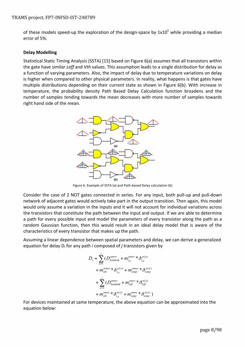
Statistical Static Timing Analysis (SSTA) [15] based on Figure 6(a) assumes that all transistors within the gate have similar Leff and Vth values. This assumption leads to a single distribution for delay as a function of varying parameters. Also, the impact of delay due to temperature variations on delay is higher when compared to other physical parameters. In reality, what happens is that gates have multiple distributions depending on their current state as shown in Figure 6(b). With increase in temperature, the probability density Path Based Delay Calculation function broadens and the number of samples tending towards the mean decreases with more number of samples towards right hand side of the mean.
(a)
(b) Figure 6. Example of SSTA (a) and Path-‐based Delay calculation (b)
Consider the case of 2 NOT gates connected in series. For any input, both pull-‐up and pull-‐down network of adjacent gates would actively take part in the output transition. Then again, this model would only assume a variation in the inputs and it will not account for individual variations across the transistors that constitute the path between the input and output. If we are able to determine a path for every possible input and model the parameters of every transistor along the path as a random Gaussian function, then this would result in an ideal delay model that is aware of the characteristics of every transistor that makes up the path.
Assuming a linear dependence between spatial parameters and delay, we can derive a generalized equation for delay Di for any path i composed of j transistors given by
)**
*(
**
*(
)()(
)(
1nominal
)()(
)(
1nominal
antemp
nmostemp
anv
nmosvth
anleff
j
a
nmosleff
nmos
aptemp
pmostemp
apv
pmosvth
apl
j
a
pmosl
pmosi
mm
mD
mm
mDD
th
th
effeff
δδ
δ
δδ
δ
++
++
++
+=
∑
∑
=
=
For devices maintained at same temperature, the above equation can be approximated into the equation below:

TRAMS project, FP7-‐INFSO-‐IST-‐248789
page 9/98
*)(*
)**
(*
*(
nominalnominal
)()(1
nominal)(
)(
1nominal
temptemp
nmospmos
anv
nmosvth
anleff
nmosleff
j
a
nmosapv
pmosvth
apl
j
a
pmosl
pmosi
mDDj
mm
Dm
mDD
th
th
effeff
δ
δδ
δ
δ
+
++
++
++
+=
∑
∑
=
=
Solving the above equation for the solution of the form Y=Xb+ϵ and estimating b=YX-‐1
*)(* nominalnominal
)()()()(
)2()2()2()2(
)1()1()1()1(
temptempnmospmos
nmosvth
nmosleff
pmosvth
pmosleff
jnv
jnl
jpv
jpl
nv
nl
pv
pl
nv
nl
pv
pl
i
mDDj
mmmm
D
thefftheff
thefftheff
thefftheff
δ
δδδδ
δδδδ
δδδδ
+++
Χ=
Energy Modelling
The total energy for any operation (read, write & precharge) can be derived as:
Circuit level simulators like HSPICE do not provide a direct method to estimate switching energy. We compute the integral of the current through the supply over the entire time period and over the time period there is zero-‐activity (idle period) and we subtract the latter from the former to compute the switching energy. This method also provides means of computing the short-‐circuit and static energy components accurately. The total energy of the cache is derived as:
blockinactive
cellcellsinactive
controlcellactiveblinecellactivewline
cellactiveDecoderDrivermuxcolumnprecharge
Energy EnmfEpnm
EEmEpnEpEEEE
Cache −
−
−−
−
+⎥⎥⎥
⎦
⎤
⎢⎢⎢
⎣
⎡
−−+
+−+−+
++++
= *),(
))(1(
)1()(
*)(
)/(
)/()/(
)/(
where m is the number of rows, n the number of columns and p the number of active cells and f(m,n) is a function of m and n.
The empirical results extracted from the simulated are then fitted to a polynomial best-‐fit. This is a cumbersome process as the total dimensions of the regression are very large. The dimensions are then reduced through a process called main-‐effect analysis as shown in the equation below.

TRAMS project, FP7-‐INFSO-‐IST-‐248789
page 10/98
[ ]
)],,(),,([)],,(),,([
),,(),,(
0
00
00
nomnomddnomnomdd
nomnomddnomdd
nomnomddnomddEnergy
TVxfTVxfTVxfTVxf
TVxfTVxf
−−
−
−−
−+
−+
−≅
δ
Error analysis
The error is computed between energy and delay estimates obtained using the proposed models and Hspice. In the case of delay, the maximum percentage error oscillates between 6 and 10% while the median error is less tha 2% in most cases. It has to be mentioned that the percentage error is independent of the temperature. At higher temperatures the number of access time failures increases thereby reducing the total number of successful samples for post-‐simulation processing.
Figure 7. Distribution of error rates on access time computation
As energy has a very strong dependence on supply voltage, the simulation was performed for 500 samples across a range of 5 supply voltages and 9 temperatures. In most cases the error is well within 5% indicating the goodness of the fit. Only in the 0.7V range the percentage error is unusual which can be attributed to the non-‐linearity. This can be eliminated by using cubic splines of higher order polynomials.
Figure 8. Distribution of error rates for energy computation
0 2 4 6 8 10 12
30 40 50 60 70 80 90 100 110
% Error fo
r Access T
ime
Temperature
Median
0 1 2 3 4 5 6 7 8
0 5000 10000 15000 20000 25000
Percentage Error for
Energy
Sample Number
1.0V 0.9V 0.8V 0.7V 0.6V
TRAMS project, FP7-‐INFSO-‐IST-‐248789
page 11/98
4.1.2. Impact of process, voltage and temperature variations on delay and energy
Impact of Temperature on Access Time Delay
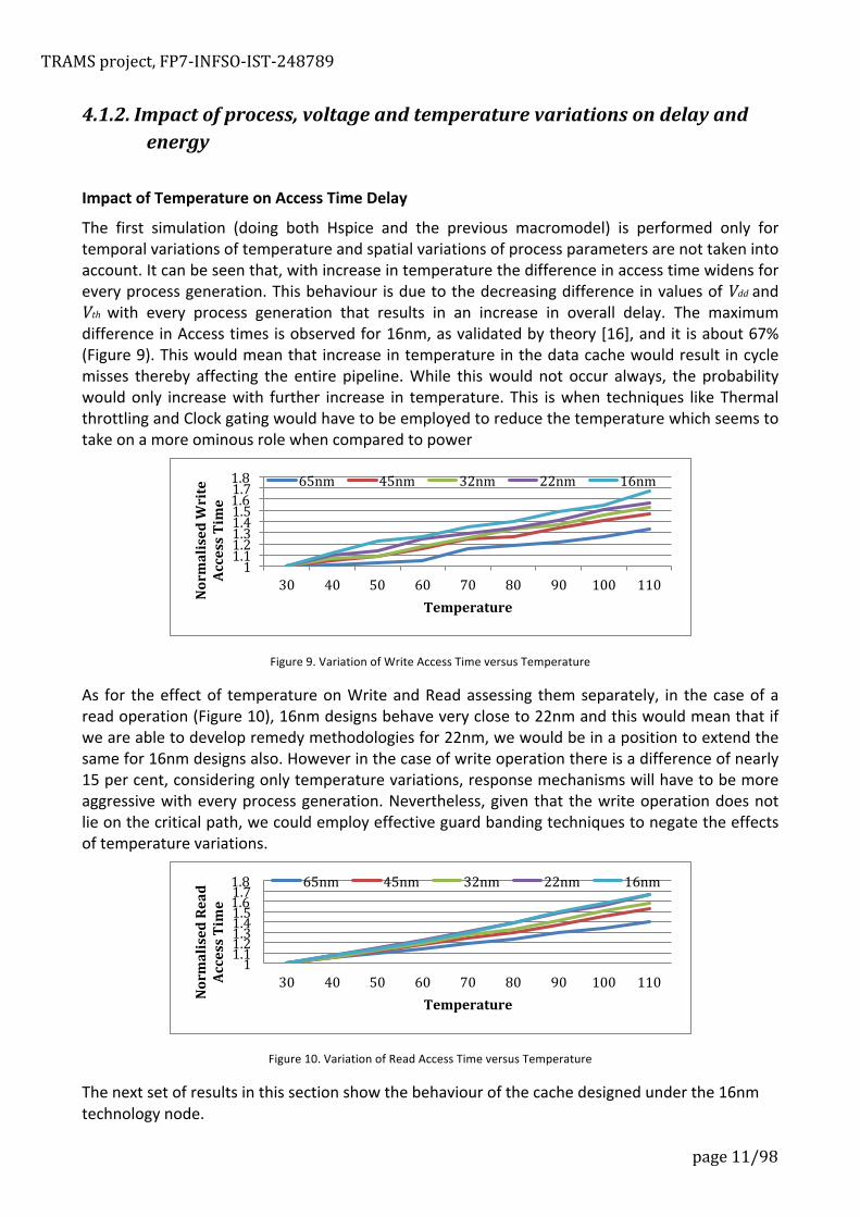
The first simulation (doing both Hspice and the previous macromodel) is performed only for temporal variations of temperature and spatial variations of process parameters are not taken into account. It can be seen that, with increase in temperature the difference in access time widens for every process generation. This behaviour is due to the decreasing difference in values of Vdd and Vth with every process generation that results in an increase in overall delay. The maximum difference in Access times is observed for 16nm, as validated by theory [16], and it is about 67% (Figure 9). This would mean that increase in temperature in the data cache would result in cycle misses thereby affecting the entire pipeline. While this would not occur always, the probability would only increase with further increase in temperature. This is when techniques like Thermal throttling and Clock gating would have to be employed to reduce the temperature which seems to take on a more ominous role when compared to power
Figure 9. Variation of Write Access Time versus Temperature
As for the effect of temperature on Write and Read assessing them separately, in the case of a read operation (Figure 10), 16nm designs behave very close to 22nm and this would mean that if we are able to develop remedy methodologies for 22nm, we would be in a position to extend the same for 16nm designs also. However in the case of write operation there is a difference of nearly 15 per cent, considering only temperature variations, response mechanisms will have to be more aggressive with every process generation. Nevertheless, given that the write operation does not lie on the critical path, we could employ effective guard banding techniques to negate the effects of temperature variations.
Figure 10. Variation of Read Access Time versus Temperature
The next set of results in this section show the behaviour of the cache designed under the 16nm technology node.
1 1.1 1.2 1.3 1.4 1.5 1.6 1.7 1.8
30 40 50 60 70 80 90 100 110
Normalised Write
Access Time
Temperature
65nm 45nm 32nm 22nm 16nm
1 1.1 1.2 1.3 1.4 1.5 1.6 1.7 1.8
30 40 50 60 70 80 90 100 110
Normalised Read
Access Time
Temperature
65nm 45nm 32nm 22nm 16nm

TRAMS project, FP7-‐INFSO-‐IST-‐248789
page 12/98
Impact of Process Variations and Temperature on Access Time Delay
Figure 11. Access Time Deviation under Spatio Temporal Variation
The black dots indicate the variation of access time for a gold-‐memory-‐system under temperature variations and the results for access time variation under spatio-‐temporal variations is indicated with coloured lines. From the above Figure 11, it can be clearly seen that less than 1% die perform better than no-‐variation dies under temperature constraints. While this could also point the deficiencies in the distribution adopted, delving deeper into the issue, we realize that the access time does not depend on SRAM cell variation alone but also the peripheral circuitry. It just means that, even if the SRAM array is designed to be variation-‐aware, it might not be the same with the peripheral circuitry. Every single block’s distribution needs to be understood at a more fine grain level to delve further deep into the distribution. Another observed phenomenon is the difference in access times for the same dies across different temperature. At lower temperatures the worst case difference is only 15% as opposed to the nearly 50% deviation at maximum temperatures. This would only mean that techniques such as speed binning which are currently used will not cater to the requirements posed by these technologies. No technique proposed at the moment would be able to compensate for a difference of the order of 50%.
0.9
1.1
1.3
1.5
1.7
1.9
2.1
1 51 101 151 201 251
Normalised
Access T
ime
Die ID
30°C 40°C 50°C 60°C 70°C 80°C 90°C 100°C 110°C
Zero Spatial Variation

TRAMS project, FP7-‐INFSO-‐IST-‐248789
page 13/98
Figure 12. Impact of Periphery Variability on Access Time deviation
At lower temperatures, each of the components is fast to respond and this can be validated by the fact that the control circuitry contributes to nearly 50% of the delay. This does not mean that the control circuitry is easily affected by the temperature. It means on a relative basis, the control circuitry which is made up of a very small number of devices decides the overall delay. As the temperature decreases, the contribution to access times due to control circuitry decreases while the other circuits are easily affected by temperature variations. When we normalized all the bars to 1, not shown here, the contribution of control circuit was only 36% at 110 oC when compared to the 50% contribution at 30 oC. It is clear that the Pre Decoder is the most affected by temperature in both cases -‐ write and read. In the case of the read cycle, as the temperature increases the effect of temperature on the Sense Amplifier becomes important. From the above 2 inferences, we can draw the conclusion that structures that are made up of smaller number of transistors driving large loads are likely to be more susceptible to Temperature variations when compared to structures made up of more number of Transistors.
Energy Analysis
Figure 13 and Figure 14 present energy estimates for different technologies and different supply voltages, normalized to the value at 0.6V of 22nm tech node. It is evident from the plot that the potential benefits of scaling supply voltage is a quantum reduction in the energy consumption and with reducing feature sizes the reduction is greater.
0
0.4
0.8
1.2
1.6
2
30 40 50 60 70 80 90 100 110
Normalised Read Access
Time
Temperature
Control Predecoder Row Decoder Column Mux + Sense AmpliQier
0
0.5
1
1.5
2
30 40 50 60 70 80 90 100 110
Normalised Write
Access
Temperature
Control Predecoder Row Decoder Wordline + Write Driver

TRAMS project, FP7-‐INFSO-‐IST-‐248789
page 14/98
Figure 13. Normalized energy consumption for several voltage levels and technologies
0
5
10
15
20
20
40
60
80
100
120
1V0.9V
0.8V0.7V
0.6V
Nor
mal
ised
Ene
rgy
Con
sum
ptio
n
Tempe
ratur
e
Supply Voltage
Figure 14. Normalized energy consumption for different supply voltages and temperatures for the 22nm technology node.
It should be noted in this case that a significant portion of energy consumption is due to leakage and not accounting for temperature variations results in under estimation of leakage energy. While dynamic power to great extent is dependent on the supply voltage, not accounting for variation in sub-‐threshold leakage due to temperature variations leads to gross underestimation of total energy. While, procedures like burn-‐in and post-‐fabrication tuning have the same functionality, they require prototype chips which are seldom available at early design stages. This analysis will help alleviate this issue by providing accurate energy estimates for chips in future technologies.
4.1.3. Effect of fine-‐grain Vth tunning While the previous section has analyzed the performance (in terms of delay and energy) of the cache design under process, voltage and temperature variations; in this section we analyze the use of Vth fine tunning as a first approach to reduce the spread in delay and energy consumed.
Using the energy and delay models proposed, we performed statistically 2 different circuit optimizations to evaluate their energy-‐delay tradeoffs. In the first case, different threshold voltage were assigned to delay and energy critical regions. While the peripheral circuitry was assigned a lower threshold, the threshold of memory array was not changed to make sure the leakage is minimal. While the delay improvement was minimal at lower temperatures, at higher temperature the speed was improved by 18%.
0
5
10
15
20
22nm
32nm
45nm
1V0.9V
0.8V0.7V
0.6VNor
mal
ised
Ene
rgy
Con
sum
ptio
n
Tech
nolog
y
Supply Voltage

TRAMS project, FP7-‐INFSO-‐IST-‐248789
page 15/98
In the other case, the standby supply voltage of unaccessed blocks was reduced by nearly 40% while assigning multiple threshold to the periphery and memory access. Under worst case process variations while the chip is maintained at 80 degrees, the energy per access was reduced by nearly 50%.
Temperature
Nor
mal
ised
Acc
ess
Tim
e
0.0
0.2
0.4
0.6
0.8
1.0
1.2
1.4
1.6
1.8
30 40 50 60 70 80 90 100 110
HSPICE (No spatial variation)
HSPICE (5% Vth reduction)Model (10% Vth reduction)
Model (5% Vth reduction)
HSPICE (10% Vth reduction)
Control CircuitryArr. Sub-Block DecoderRow DecoderBit Line Driver
Standby Supply Voltage
1V 0.9V 0.8V 0.7V 0.6V
% E
nerg
y C
onsu
mpt
ion
0
20
40
60
80
100
120No Dual VthVth, (Vth+5%) ConfigurationVth, (Vth+10%) Configuration
Figure 15. Normalized access time and energy consumption for fine grain tunning of Vth for different blocks of the cache
This analysis suggests that finetunning the Vth may drastically reduce energy consumption for unused blocks (i.e. leakage) and it may help mitigate the widespread of access time delays caused by temperature variations. This opens a promising set of techniques that will be analyzed and reported in the next deliverables.
4.1.4. Conclusions
An accurate macro-‐model to evaluate delay and energy in a complete 32kB memory has been implemented and applied to the case of a 6T bit-‐cell SRAM. The impact of temperature is very high, in general for all technologies and specifically for deeper technologies. For a device sized design the read and write access time for the memory increases a 60% per a change of temperature from 25 to 110 oC. Supply voltage are also impacting, around a 15% of delay for a 10% of VDD fluctuation. Process variability, both systematic and random have been taken into account, shown a very high impact to delay. Energy consumption has also been evaluated for all the set of fluctuating variables and it has been shown that a fine-‐tuning of Vth may drastically reduce energy consumption.
4.2. Robustness analysis of 6T SRAM cell 4.2.1. The 6T SRAM bit-‐cell A typical 6T SRAM cell uses two identical crossed coupled inverters and two access transistors as shown in Figure 16. The access transistors allow access to the cell during read and write operations and assure cell isolation during the data retention mode.
The parametric failures in SRAMs are due to systematic and random process parameter variations. The systematic variation in a parameter modifies the value of that parameter for all transistors in a die in the same direction. The random variations shift the process parameters of different transistors in a die in different directions. While circuit techniques have been developed to

TRAMS project, FP7-‐INFSO-‐IST-‐248789
page 16/98
compensate for the global systematic die-‐to-‐die variations [17], the local random variations cannot be as easily compensated and they have a significant effect on the SRAM yield because of the asymmetry introduced between the matched transistors of an SRAM cell [18], [19], [20]. Among the different sources of random intra-‐die variations, the most significant one are the threshold voltage (VTH) due to Random Dopant Fluctuation (RDF) and Line Edge Roughness (LER).
Physical failure mechanisms caused by process variations (parametric failures) in a SRAM bit-‐cell are [21]: hold failure, read failure, access failure and write failure. In Figure 16a, the transistors that affect each of these failures are marked and in Figure 16b, the failure mechanisms together with the correct operation are illustrated.
A Hold Failure (HF) can occur in data retention mode, when the supply voltage of the cell is decreased to reduce the leakage power consumption. If lowering the VDD causes the data stored in the cell to be destroyed, the cell is said to have hold failure. Asymmetry in the cross coupled inverters increases the failure probability, the hold failure probability depends on variation in any of the NL, PL, NR and PR transistors.
The Read Failure (RF) occurs if the data stored by the cell is destroyed during the read mode, i.e. the zero level degradation at the R node, becomes larger than the trip voltage of the inverter (NL&PL). Hence the read failure probability is affected by the variability in the pull down (NR) and access transistor (NaR) at the ‘0’ storing node as they directly affect the zero level degradation, and the pull down (NL) and pull up (PL) transistors at the ‘1’ storing node as they affect the trip voltage of the resulting inverter.
An Access Failure (AF) occurs during the read operation if the differential bit line voltage (∆BL = VBL – VBLB) does not reach the desired value (typically 10%VDD) during the access time (Taccess) of the cell. In read mode, the bit line BLB is partially discharged through the access transistor NaR and the pull down transistor NR (VBLB = VDD – ∆V), while the bit line BL maintains the pre-‐charged value (VBL = VDD). The differential bit line voltage and hence the access failure probability is affected by the variability in the two transistors.
An unsuccessful writing of the cell is referred to as a Write Failure (WF). This occurs when the voltage at the ‘1’ storing node (L) does not decrease enough to flip the state of inverter (NR&PR). The write failure probability is determined by the variability in the pull up (PL) and access transistor (NaL) at the ‘1’ storing node as they affect the voltage level at node L and the pull down (NR) and pull up (PR) transistors at the ‘0’ storing node as they affect the trip voltage of the resulting inverter.
Figure 16 a. The standard 6T SRAM bit – cell, b -‐ 6T SRAM operation modes, illustrating the failures in each mode:
read/access/write/hold
BL BLB
NaRNaL PL PR
NRNLL
R
WL
Read
Access
Write
Hold
‘1’‘0’
VL, VR
Time0
1
READ FAILURE
VL, VR
Time0
1
WRITE FAILURE
VL, VR
Time0
1
HOLD FAILURE
BL, BLB
Time0
1
ACCESS FAILURE
TaccessTaccess
Taccess
VDDlow
∆BL = 10%VDD
Failure
Correct Operation

TRAMS project, FP7-‐INFSO-‐IST-‐248789
page 17/98
The failure probability of an SRAM cell (Pcell) is given by the probability that at least one of the above mentioned failures occur. Since only the failures due to random variations are considered in this analysis, it can be assumed that the failure of any cell in the memory array is independent of the failure of any other cell in the array. Hence, the SRAM array failure probability Parray is given by:
( )Ncellarray P11P −−= Equation 1
where Pcell is the failure probability of a single cell and N is the number of cells in the array. The parametric yield of the SRAM array is:
( )Ncellarrayparam P1P1Y −=−= Equation 2
4.2.2. Statistical analysis of the SRAM cell Increased process variability in nano-‐scaled technologies is becoming a critical challenge for CMOS design. Process variability can be classified as inter-‐die and intra-‐die, and it is due to the fabrication process and to the non-‐uniform conditions during dopant deposition or diffusion resulting in high variability in transistor parameters.
Because of its speed and compatibility with standard logic process, SRAM is the embedded memory of choice for many VLSI systems [22]. According to ITRS 2009 [23], the area of the 6T SRAM cell will decrease from 0.11µm2 to 0.012 µm2 between 2010 and 2015 (SRAM density can reach over 5 billion transistors / cm2, by 2015) [23]. In order to meet the small area requirement, SRAM bit-‐cells are designed with minimum (or near minimum) sized transistors, which increases their sensitivity to process variations. The major concerns regarding embedded SRAM memory as technology scales are increased static power, lower cell stability, and reduced operating margins, robustness and reliability [22]. The increase in variability aggravates all these problems, and hence statistical analysis methods considering process parameter variation become mandatory for memory robustness estimation.
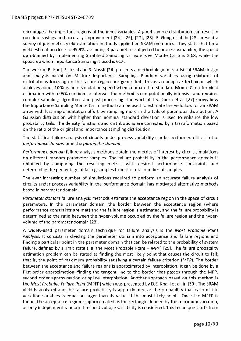
Following, an overview of widely used techniques for statistical failure analysis of circuits under process variability will be presented, with special emphasis on those suitable for SRAMs.
The most common statistical failure analysis methodology for circuits under process variability is based on Monte Carlo (MC) simulation. Monte Carlo methods are a class of computational algorithms that rely on repeated random sampling to determine failure statistics. The accuracy of the statistical failure analysis depends on the sample size, so for extremely small failure probability events (as in the case of an idle SRAM cell at nominal supply voltage) the number of random experiments to accurately estimate this probability is extremely large (the sample size must be quadrupled to achieve twice the accuracy) [24].
Extensive research has been devoted to the reduction of sample size for speed improvement while maintaining the accuracy of standard Monte Carlo simulations. One of the resulting methods is the Stratified Sampling technique [25], which consists in stratifying the sample space by choosing a partition of the input parameter space. The integrals in each stratum are than estimated and combined to obtain the overall integral. Another common method of SRAM analysis is Importance Sampling [26], [27]. It is based on the fact that certain values of the input random variables have more impact on results than others. In Importance Sampling the statistical distribution function is transformed to increase the probability of occurrence of significant values. The use of biased distributions will result in a biased estimator. The simulation outputs are weighted to correct the biased distribution and ensure that the new importance sampling estimator is unbiased. The issue in implementing importance sampling simulation is the choice of the biased distribution which
TRAMS project, FP7-‐INFSO-‐IST-‐248789
page 18/98
encourages the important regions of the input variables. A good sample distribution can result in run-‐time savings and accuracy improvement [24], [26], [27], [28]. F. Gong et al. in [28] present a survey of parametric yield estimation methods applied on SRAM memories. They state that for a yield estimation close to 99.9%, assuming 3 parameters subjected to process variability, the speed up obtained by implementing Stratified Sampling vs. extensive Monte Carlo is 3.6X, while the speed up when Importance Sampling is used is 61X.
The work of R. Kanj, R. Joshi and S. Nassif [26] presents a methodology for statistical SRAM design and analysis based on Mixture Importance Sampling. Random variables using mixtures of distributions focusing on the failure region are generated. This is an adaptive technique which achieves about 100X gain in simulation speed when compared to standard Monte Carlo for yield estimation with a 95% confidence interval. The method is computationally intensive and requires complex sampling algorithms and post processing. The work of T.S. Doorn et al. [27] shows how the Importance Sampling Monte Carlo method can be used to estimate the yield loss for an SRAM array with less implementation effort by sampling more in the tails of parameter distribution. A Gaussian distribution with higher than nominal standard deviation is used to enhance the low probability tails. The density functions and distributions are corrected by a transformation based on the ratio of the original and importance sampling distribution.
The statistical failure analysis of circuits under process variability can be performed either in the performance domain or in the parameter domain.
Performance domain failure analysis methods obtain the metrics of interest by circuit simulations on different random parameter samples. The failure probability in the performance domain is obtained by comparing the resulting metrics with desired performance constraints and determining the percentage of failing samples from the total number of samples.
The ever increasing number of simulations required to perform an accurate failure analysis of circuits under process variability in the performance domain has motivated alternative methods based in parameter domain.
Parameter domain failure analysis methods estimate the acceptance region in the space of circuit parameters. In the parameter domain, the border between the acceptance region (where performance constraints are met) and the failure region is estimated, and the failure probability is determined as the ratio between the hyper-‐volume occupied by the failure region and the hyper-‐volume of the parameter domain [28].
A widely-‐used parameter domain technique for failure analysis is the Most Probable Point Analysis. It consists in dividing the parameter domain into acceptance and failure regions and finding a particular point in the parameter domain that can be related to the probability of system failure, defined by a limit state (i.e. the Most Probable Point – MPP) [29]. The failure probability estimation problem can be stated as finding the most likely point that causes the circuit to fail; that is, the point of maximum probability satisfying a certain failure criterion (MPP). The border between the acceptance and failure regions is approximated by interpolation. It can be done by a first order approximation, finding the tangent line to the border that passes through the MPP, second order approximation or spline interpolation. Another approach based on this method is the Most Probable Failure Point (MPFP) which was presented by D.E. Khalil et al. in [30]. The SRAM yield is analysed and the failure probability is approximated as the probability that each of the variation variables is equal or larger than its value at the most likely point. Once the MPFP is found, the acceptance region is approximated as the rectangle defined by the maximum variation, as only independent random threshold voltage variability is considered. This technique starts from

TRAMS project, FP7-‐INFSO-‐IST-‐248789
page 19/98
the hypothesis that SRAM cell failure is due only to independent random process variations and the failure metric is monotonic with each parameter variation. The method requires finding the combination of input variations maximizing the failure probability.
A recent proposal for statistical failure analysis in the parameter domain is the Yield Estimation Nonlinear Surface Sampling technique (YENSS). It was first presented by S. Srivastava and J. Roychowdhury in [31] and then improved by C. Gu and J. Roychowdhury in [32]. The method locates the failure region boundary in the parameter domain and determines the failure probability as the ratio between the area (or volume) outside the bounded region and that of the parameter domain. The boundary points are determined by a local search algorithm. This technique assumes the partition of the parameters space into 2N regions (N being the number of variable parameters, i.e. the dimension of the parameter domain), and uniform distribution of process parameters. It can be used for non-‐uniform distributions as well, by converting them into uniform distributions by the corresponding Cumulative Distribution Function (CDF). The method can also be extended to correlated parameters if principal component analysis is applied first.
In [33], F. Gong et al. present a technique to improve yield estimation efficiency, the QuickYield method, which proposes a yield surface boundary determination by surface-‐point finding and global search. The performance constraints are included in the differential algebra equation that describes the circuit, resulting in an augmented system equation.
We propose a different approach to SRAM cell statistical failure analysis in the parameter domain. The following section gives a detailed description of the method.
4.2.3. The Satisfiability Boundary – Statistical Integration (SB-‐SI) Method With the proposed method of failure probability estimation, the boundary separating the acceptable performance and failure regions – Satisfiability Boundary (SB) – is found in the parameter domain, and then Statistical Integration (SI) is performed over the failure region to estimate the failure probability. It is a general methodology which can be applied to any circuit with a known distribution of process parameters and environmental variables.
The essence of the method consists in the decoupling between performance and statistics in the parameter domain. The failure probability is estimated in two steps: first, the Satisfiability Boundary separating the Acceptance Region from the Failure Region is found and second, a Statistical Integration over the two regions is performed for probability estimation. That is why the method is hereafter referred to as SB-‐SI (Satisfiability Boundary – Statistical Integration). The next subsections summarize important issues and describe the above two steps.
A. Problem statement
Process variability has a strong influence on circuit performance and failure probability. All circuits on a die are subject to both systematic and random process variations. Systematic variations are mainly introduced during the photolithography process and affect the dimensions and threshold voltage of all transistors on a die in the same direction following a certain distribution. Random variability further affects the threshold voltage mainly because of the random nature of dopant deposition (RDF). When analysing a device under process variability, systematic variation is considered first and then random variation is superimposed. Hence, the distribution of the process parameter of the device under analysis results from the combination of systematic and random variation.

TRAMS project, FP7-‐INFSO-‐IST-‐248789
page 20/98
Assuming a certain device with a parameter affected by process variability, its failure probability is given as the probability of not properly performing its specified function, while the correct operation of the device is reflected by performance satisfiability.
In order to illustrate the concepts of Acceptance and Failure regions in the parameter space, let us consider parameter spaces of one single parameter (N=1) and two parameters (N=2) before presenting the general case with N parameters. Assuming only one device parameter is affected by process variability, there is a range of values for which the device meets the required performance (acceptance region in the parameter domain) whereas for the remaining values the system fails (failure region in the parameter domain). Once the two regions are identified, the failure probability is determined considering the statistical distribution of the process parameter (upper part of Figure 17).
The same applies to the two-‐dimensional case, in which two of the circuit parameters are subject to process variation affecting its performance (lower part of Figure 17). It also applies to the general N dimensional case.
Figure 17. One & two device parameters affected by process variability (Acceptance and Failure Regions)
Assuming a circuit with N parameters (p = [param1 param2 … paramN]) subject to process variability and whose performance metric must have larger values than a given limit (Perf(p)>Pmin), the acceptance and failure regions are defined as follows:
{ } { }minmin P)(PerfFRandP)(PerfAR <=>= pppp Equation 3
where p is the N dimensional vector of process parameters: p = [param1 param2 … paramN]. The Satisfiability Boundary is the hyper-‐surface that separates the Acceptance Region (AR) from the Failure Region (FR). The Satisfiability Boundary (SB) is defined as:
{ }minP)(PerfSB == pp Equation 4
In the parameter domain, AR and FR are N dimensional hyper-‐volumes and SB is composed of N-‐1 dimensional hyper-‐surfaces. The Satisfiability Boundary is searched for in the parameter domain while for the Statistical Integration the actual parameter distribution is taken into account. Parameter distribution depends on the technology node, fabrication process and design. Therefore it is important to separate the search for the Satisfiability Boundary from the Statistical Integration.
Acceptance Region
Failure Region
min maxnominal
Acceptance RegionFailure Region
Statistical Distribution
Statistical Distribution
param1
param1
para
m2
param1param2nominal
nom
inal
min
min
max
max

TRAMS project, FP7-‐INFSO-‐IST-‐248789
page 21/98
B. Satisfiability Boundary The Satisfiability Boundary search can be very expensive and time consuming if performed by simulation, so we propose a method to estimate the SB by finding a set of boundary points (Significant Points – SP) and then interpolating to approximate the boundary surface with controllable error.
Two-‐Dimensional Analysis
To simplify the explanation of the method, a circuit with two (N = 2) parameters (p=[param1 param2]) subject to variability is considered. For illustration purposes, a 6T SRAM bit cell in data retention mode is analysed assuming that only two transistor parameters are affected by process variability.
In the parameter domain, the Satisfiability Boundary will be approximated by a polygon whose vertices (hereafter referred to as Significant Points (SP)) are obtained by simulation. An increase in the number of vertices obviously leads to a more precise boundary approximation. The first polygon that can be obtained to approximate the Satisfiability Boundary in the 2D parameter domain is a quadrilateral. In this case the Significant Points are determined by the intersection between the SB and the parameter domain axes. If the obtained quadrilateral is not a good estimate an extra set of SPs is obtained from the intersection between the SB and the lines bisecting the angles previously formed – First Angular Bisection (FAB) – (Figure 18). By further bisecting the resulting angles, more Significant Points can be determined for a more accurate approximation of the SB – Second Angular Bisection (SAB), Third Angular Bisection (TAB) and so on. Assuming the parameter domain space defined by the parameter variation, the nominal parameter point (pnom=[p1nom,p2nom]) defines the origin of the system axes, i.e. the [0,0] point. The maximum and minimum values on the two axes are given by (+∆1, -‐∆1) and (+∆2, -‐∆2) respectively.
In First Angular Bisection, a set of points is generated in the parameter domain by all possible combinations of ∆param1 = [-‐∆1 0 ∆1] and ∆param2 = [-‐∆2 0 ∆2], resulting a total of 32 (=9) points (3 is the number of values in ∆param, 2 is the number of parameters), including the [0,0] point. The search directions for the SPs are given by the vectors connecting the origin of the system axes with the resulting 9 points. In this case, the number of directions is 32-‐1 (=8) (left side of Figure 4.2.3). The same algorithm applies for the Second Angular Bisection. The points are obtained by all possible combinations of ∆param1 = [-‐∆1 -‐∆1/2 0 ∆1/2 ∆1] and ∆param2 = [-‐∆2 -‐∆2/2 0 ∆2/2 ∆2], resulting a total number of 52 (=25) points. To avoid redundancy, the inner points are eliminated and the number of directions is given by 52-‐32 (=16) (right side of Figure 18). The algorithm can be extended to higher-‐levels of angular bisection.
Once the directions are established, the intersection points are found using a search algorithm. For this particular case, the bisection method was chosen for its robustness and simplicity. The equation Perf(p)-‐Pmin=0 is solved for the variable p (p is given by a point in the parameter domain p = [p1 p2]). Two initial points p1 and p2 are required such that Perf(p1)-‐Pmin and Perf(p2)-‐Pmin have opposite signs (in other words, one of the points must be in the Acceptance Region and the other in the Failure Region). The method divides the vector [p1 p2] into two equal parts by computing pm=(x1+x2)/2 and verifies if pm satisfies Perf(pm)-‐Pmin=0. Otherwise, according to the sign of Perf(pm)-‐Pmin, p1 or p2 takes the value of pm and the algorithm continues until the desired precision is reached. The maximum absolute geometric error (εg) after n steps is
1ng 2 +
−=
p2p1ε Equation 5
TRAMS project, FP7-‐INFSO-‐IST-‐248789
page 22/98
where |p1-‐p2| indicates the module of the vector p1-‐p2. The maximum number of iterations required for certain accuracy (εg) is given by
1logng
2 −⎥⎥⎥
⎤
⎢⎢⎢
⎡ −=
ε
p2p1 Equation 6
In Equations 5 and 6, p1 and p2 are the vectors with which the algorithm starts (initial points)
Figure 18. Directions for Significant Point search in First and Second Angular Bisection
The bisection method is applied separately for each direction to find all the Significant Points of the Satisfiability Boundary.
For a given error, the maximum number of simulations for each point is given by Equation 6. In all cases, the point p1 is chosen to be the origin of the system axes (p1=[p11 p21]=[0,0]) and the vectors p2 (p2=[p12 p22]) are given by the extremes. The first column of Tables 1 and 2 (Figure 19) contains the initial points p1, p2 for the bisection method; the second, the resulting Significant Points (which are also illustrated in the left figures) and the third, the modules |p1-‐p2|, which determine the number of simulations needed to obtain the corresponding SPs with a certain accuracy. The points marked by circles (SP1÷SP4) and triangles (SP5÷SP8) are obtained at the intersection between SB and the system axes and by first angular bisection, respectively.
The number of Significant Points, and consequently the number of simulations, increases with increasing the number of parameters, i.e. the dimension of the parameter space (N). In the 2D case under study, the Satisfiability Boundary can be approximated by the polygon obtained when applying an interpolation algorithm on the set of Significant Points (Figure 19b). The first step to obtain the polygon is to find the adjacent points, which is intuitive for the two-‐dimensional case but gets challenging for higher dimensions. The algorithm used in this work, which is extensible to the general N dimensional case, is described below for two dimensions.
In the quadrilateral approximation, the interpolation is straightforward, as the SPs are given by the intersection of the SB with the axes. For the first-‐ and higher-‐order angular bisection approximations, the problem becomes more complex and an algorithm must be implemented. To begin with, the extreme points in the parameter domain are mapped (the +∆ values are mapped to 1 and the -‐∆ values are mapped to -‐1), as shown in Table 2 of Figure 19b. Starting the search from the [1, 1] point, half of the adjacent points are found by decrementing by 1 for each variable and the other half is found starting from the [-‐1,-‐1] point and incrementing by 1 in each direction (diagram of Figure 19b). Two points form a straight line. Thus, by connecting the adjacent points two by two the polygonal estimate of the Satisfiability Boundary is obtained.
The general equation of a straight line is given by
[- ∆ -∆/2 0 ∆/2 ∆]
[-∆
-∆/
2
0 ∆/
2 ∆]
[-∆ 2
0 ∆ 2
][-∆1 0 ∆1]
∆param1 = [-∆1 0 ∆1]∆param2 = [-∆2 0 ∆2]
∆param1 = [-∆1 -∆1/2 0 ∆1/2 ∆1]∆param2 = [-∆2 -∆2/2 0 ∆2/2 ∆2]
∆param1
∆param2
∆param1
∆param2
First Angular Bisection Second Angular Bisection

TRAMS project, FP7-‐INFSO-‐IST-‐248789
page 23/98
1pbpa 21 =⋅+⋅ Equation 7
The a and b coefficients for each of the straight lines forming the polygon are determined by solving the system
⎥⎦
⎤⎢⎣
⎡=⎥
⎦
⎤⎢⎣
⎡•⎥⎦
⎤⎢⎣
⎡11
ba
pppp
2212
2111 Equation 8
where (p11,p21) and (p12, p22) are the coordinates of two of the adjacent points. After obtaining the entire set of straight lines, the boundary polygon defined by the set of all a and b coefficients is obtained.
An increase in the number of Significant Points leads to improved accuracy of the boundary approximation but also to a larger number of simulations, that is, a longer estimation time. As can be seen, there is a tradeoff between accuracy and speed.
Figure 19a. Choice of the Significant Points on the Satisfiability Boundary: Quadrilateral and Octagon Approximations b. Finding the
adjacent Significant Points on the Satisfiability Boundary: Quadrilateral and Octagon Approximations
Once the polygonal approximation of the SB is obtained, the acceptance and failure regions are found. The condition that a random point in the parameter domain is in the acceptance region or the failure region is given by
01pbpa)b,a(allforifFR)y,x(01pbpa)b,a(allforifAR)y,x(
21
21
>−⋅+⋅∈
<−⋅+⋅∈ Equation 9
Based on the above parameter domain partition, the failure probability is determined by Statistical Integration (SI). A brief analysis of the Satisfiability Boundary approximation in the general N dimensional case is presented next.
N Dimensional Analysis
The steps described in the two dimensional case are also followed for the N dimensional (N parameters subject to variability, p = [param1 param2 … paramN]) approximation of the Satisfiability Boundary. The Significant Points on the SB are determined by the same bisection method. The first approximation is performed by intersecting the axes with the SB, which results in a 2N vertex hyper-‐polygon. Then, the angular bisection starts. Following the algorithm explained for the two-‐dimensional case in the previous subsection, and illustrated in Figure 18, the number of Significant Points depending on the level of angular bisection for the N dimensional approximation of the SB can be determined (Table 3). The number of elements in each ∆param is (2M+1), M being the order of angular bisection. The resulting number of points assuming N
[0,0], [-∆1,0] →SP1 |p1-p2| = ∆1
[0,0], [0,+∆2] →SP2 |p1-p2| = ∆2
[0,0], [+∆1,0] →SP3 |p1-p2| = ∆1
[0,0], [0,-∆2] →SP2 |p1-p2| = ∆2
Table 1 – Quadrilateral Approximation
[0,0], [-∆1,0] →SP1 |p1-p2| = ∆1
[0,0], [-∆1, -∆2] →SP5 |p1-p2| = sqrt(∆12+∆2
2)[0,0], [0,+∆2] →SP2 |p1-p2| = ∆2
[0,0], [+∆1, +∆2] →SP6 |p1-p2| = sqrt(∆12+∆2
2)[0,0], [+∆1,0] →SP3 |p1-p2| = ∆1
[0,0], [+∆1, -∆2] →SP7 |p1-p2| = sqrt(∆12+∆2
2)[0,0], [0,-∆2] →SP4 |p1-p2| = ∆2
[0,0], [-∆1, -∆2] →SP8 |p1-p2| = sqrt(∆12+∆2
2)
Table 2 – Octagon Approximation
∆ p1
SP1
SP2
SP3
SP4
SP1
SP4
SP3
SP2
SP8 SP7
SP6SP5
∆p2
∆ p1
∆p2
SB
0,1 1,0
-1,0 0,-1
-1+1[0,0]
-1,1 1,-1
1,1
0,1 1,0
-1,-1
-1,0 0,-1
-1+1
[0,0]
SP1 →[-∆1,0] →[-1,0]
SP5 →[-∆1, -∆2] →[-1,-1]
SP2 →[0,+∆2] →[0, 1]
SP6 →[+∆1, +∆2] →[1, 1]
SP3 →[+∆1,0] →[1,0]
SP7 →[+∆1, -∆2] →[1, -1]
SP4 →[0,-∆2] →[0, -1]
SP8 →[-∆1, -∆2] →[-1, -1]
SP1 →[-∆1,0] →[-1,0]
SP2 →[0,+∆2] →[0, 1]
SP3 →[+∆1,0] →[1,0]
SP4 →[0,-∆2] →[0, -1]
Table 2 – Octagon Approximation
Table 1 – Quadrilateral Approximation

TRAMS project, FP7-‐INFSO-‐IST-‐248789
page 24/98
parameters subjected to variability is (2M+1)N. To avoid redundancy the inner points are eliminated (-‐(2M-‐1)N) and the total number of search direction for the SPs is obtained. The algorithm of finding the adjacent Significant Points on the Satisfiability Boundary for the first angular bisection in a 3D analysis is the same as for the 2D analysis. The search starts from the [1,1,1] point, half of the adjacent points are found by decrementing by 1 for each variable and the other half are found starting from the [-‐1,-‐1,-‐1] point and incrementing by 1 for each variable (diagram in Figure 20). The hyper-‐polygon estimation of the Satisfiability Boundary for different levels of angular bisection in a 3D analysis is illustrated in Figure 21.
Once the Significant Points are found, the SB can be approximated by a hyper-‐surface. The adjacent points must be connected similarly to obtain the hyper-‐surface estimating the SB. Equations 7 and 8 become:
1papapa NN2211 =⋅++⋅+⋅ Equation 10
⎥⎥⎥
⎦
⎤
⎢⎢⎢
⎣
⎡
=
⎥⎥⎥
⎦
⎤
⎢⎢⎢
⎣
⎡
•
⎥⎥⎥
⎦
⎤
⎢⎢⎢
⎣
⎡
1
1
a
a
pp
pp
N
1
NNN1
1N11
Equation 11
The rules in Equation 7, for the N dimensional case become:
01pa)aa(allforifFR)xx(
01pa)aa(allforifAR)xx(
N
1iiiN1N1
N
1iiiN1N1
>−⋅∈
<−⋅∈
∑
∑
+
+
Equation 12
As previously mentioned, the proposed method of failure probability estimation consists in finding the Satisfiability Boundary and then Statistically Integrating the probability density function over the failure region to estimate the failure probability. The statistical integration is described in the following subsection.
Approximation Number of Significant Points
2N vertices hyper-‐polygon
2N
M-‐th Angular Bisection (2M+1)N – (2M–1)N
2D 3D 4D 6D 8D 10D
First Angular Bisection 8 26 80 728 6560 59048
Second Angular Bisection
16 80 544 14897 384065 9706577
Third Angular Bisection 32 242 4160 102024 5374176 272709264
Table 3. Number of SP in N Dimensional Analysis for Different Levels of Angular Bisection

TRAMS project, FP7-‐INFSO-‐IST-‐248789
page 25/98
Figure 20 a. Finding the adjacent Significant Points on the Satisfiability Boundary: First Angular Bisection (26 SPs) in 3D
analysis
Figure 21 b. The polygonal estimation of the Satisfiability Boundary for different levels of angular bisection (3D)
C. Statistical Integration
The parameter joint probability distribution is used to estimate the probability of satisfying the specifications. Assuming a multivariate distribution of N random variables, the joint (cumulative) distribution function is a positive, real-‐valued function, given by:
)xp,,xp,xp(P)x,x,x(F NN2211N21 ≤≤≤= Equation 13
111
011 101 110
-‐111 001 010 1-‐11 100 11-‐1
-‐101 -‐110 0-‐11 01-‐1 1-‐10 10-‐1[0,0,0]
-‐1-‐11 -‐100 0-‐10 -‐11-‐1 00-‐1 1-‐1-‐1
-‐1-‐10 -‐10-‐1 0-‐1-‐1
-‐1-‐1-‐1
-1+1
6 vertices hyper-polygonApproximation
First Angular Bisection
Second Angular Bisection Third Angular Bisection
∆param1 ∆param1
∆param1∆param1
∆param2 ∆param2
∆param2
∆param2
∆par
am3
∆par
am3
∆par
am3
∆par
am3
TRAMS project, FP7-‐INFSO-‐IST-‐248789
page 26/98
where p1,…,pN are the random variables under analysis. The probability density function is given by f(p1…pN). The probability that the parameter variables lie in predefined ranges (xi<pi<yi, i=1…N) between certain limits is given by
∫∫=≤≤≤≤N
N
1
1
y
xN1N1
y
xNNN111 dpdp)pp(f)ypx,ypx(P Equation 14
The parameter domain is an N-‐dimensional hyper-‐rectangle. Given the complex shapes of the two regions (AR and FR) a computational strategy in needed to determine the value of P in Equation 12. As integration over a regular, well defined space is straight forward and it is relatively easy to consider correlation [34], the parameter domain must be divided into hyper-‐rectangles. Three regions are thus obtained, i.e. Hyper-‐rectangle Acceptance Region (HAR), Hyper-‐rectangle Failure Region (HFR) and Hyper-‐rectangle Satisfiability Boundary (HSB) as shown in Figure 21 for the two-‐dimensional case. The partition is performed using a bisection-‐like method. The left side of Figure 21 illustrates the first step of space division: each edge of the initial rectangle is divided in half and, by connecting the resulting points, four rectangles are obtained.
In order to determine to which of the three regions these rectangles belong, the positions of the vertices are checked using Equation 7 (or Equation 12 for the N-‐dimensional case):
• if all vertices are inside the acceptance region, the rectangle (R) is in HAR;
• if all vertices are inside the failure region, the rectangle (R) is in HFR;
• if there are vertices both in the acceptance and failure regions, the rectangle (R) is in HSB.
Rectangles in HAR and HFR are left untouched whereas rectangles in HSB are further divided (Figure 21).
Once the space division achieves the required accuracy, the statistical integration is performed by integrating hyper-‐rectangles in the parameter domain using the statistical probability density function. By integrating the probability density function on each hyper-‐rectangle, the following probabilities are computed:
∑
∑
∑
=
=
=
∈=
∈=
∈=
nb
1iiSB
na
1iiaccept
nf
1iifail
)HSBR(PP
)HARR(PP
)HFRR(PP
Equation 15
where nf is the number of hyper-‐rectangles in the Failure Region, na is the number of hyper-‐rectangles in the Acceptance Region and nb is the number of hyper-‐rectangles on the Satisfiability Boundary.

TRAMS project, FP7-‐INFSO-‐IST-‐248789
page 27/98
Figure 22. 2D parameter domain partition into rectangles
The probability PSB determines the accuracy of the statistical integration. The space division continues until the desired accuracy is achieved (i.e. 0.1% accuracy is obtained when PSB = 0.1%Paccept). Different applications have different requirements in terms of accuracy and speed of the failure probability estimation. For example, when comparing designs the failure probability must be estimated as fast as possible without very strong restrictions on accuracy, as only relative values are important. On the other hand, for yield loss estimation, the failure probability must be determined both quickly and very accurately. There are two ways to improve the accuracy of the SB-‐SI method: by finding more points on the Satisfiability Boundary and by making the HSB region as small as the accuracy requires. The following section describes the application of the SB-‐SI method for SRAM failure probability estimation in data retention mode. Accuracy and speed results are compared with Monte Carlo simulation.
4.2.4. Statistical Robustness Analysis of the 6T SRAM Cell The parametric yield estimation of a SRAM array is based on determining the failure probability in hold/read/write/access modes using dynamic failure criteria assuming random threshold voltage variation (p = ∆VTH). In read mode, the access transistors are turned on by increasing the word line voltage to VDD. The bit lines (BL and BLB) are pre-‐charged to VDD. During the read operation the bit line (BLB) corresponding to the ‘0’ sorting node discharges through the access transistor (NaR) and the pull down transistor (NR) – Figure 16. In the read mode, two failures can occur: read failure and access failure. The Read Failure (RF) occurs if the data stored by the cell is destroyed during the read mode (Figure 19). An Access Failure (AF) occurs if the differential bit line voltage (∆BL = VBL – VBLB) does not reach the desired value (typically 10%VDD) during Taccess (Figure 16b).
In write mode, the access transistors are turned on by increasing the word line voltage to VDD. The bit line voltage of BL is set to 0V, while the voltage of BLB is set to VDD. During the write operation, the node storing ‘1’ (L) discharges through the bit line (BL). Eventually the data stored by the cell flips – Figure 16a. An unsuccessful writing of the cell is referred to as a Write Failure (WF).
In data retention mode, the access transistors are turned off, and the supply voltage is decreased down to a certain value (VDDlow) in order to reduce static power consumption – Figure 16b. If lowering the VDD causes the data stored in the cell to be destroyed, the cell is said to have Hold Failure (HF).
The performance metric in read, write and hold failure analysis is given by the voltages at the nodes L and R (VL and VR): Perf = VL – VR. The performance metric in access failure analysis is
∆p1
∆p2∆p1∆p2
HFR
HAR
HSB

TRAMS project, FP7-‐INFSO-‐IST-‐248789
page 28/98
given by the bit line voltages (VBL and VBLB): Perf = VBL – VBLB. Assuming that the cell stores a ‘0’ at the R node the failure criteria is given by:
• Hold Failure: Perf(∆VTH) < 0
• Read Failure: Perf(∆VTH) < 0
• Write Failure: Perf(∆VTH) > 0
• Access Failure: Perf(∆VTH) < 10%VDD
Once the failure criteria are established, the Satisfiability Boundary is determined for each of the four failure mechanisms.
4.2.5. Results The simulation environment is HSPICE and the SRAM cell is designed using Predictive Technology Model (PTM) transistors [4] and TRAMS WP1 transistors. As the SRAM cell design is symmetrical, the application of certain design rules reduces systematic process variability significantly. That is why only random process variability is considered in the present analysis. The combination of random dopant distribution and line edge roughness has an impact on threshold voltage variability. A 6σ upper bound in the variability range of the threshold voltage is a realistic assumption for CMOS technologies (max|(∆VTH)|=6σ). The transistors dimensions, their threshold voltage and the random threshold voltage variability are summarized in Table 4, for the technology nodes considered for this analysis.
Table 4. Variability Table for different technology node and different variability degrees – the threshold voltage standard deviation
in volts for each transistor in each variability scenario is marked in blue; the situations when 6σ variability margin exceeds the nominal value of the threshold voltage are marked in red. Values correspond for minimum size devices (W/L=1), so results are and
overestimation of properly sized cell.
A. Static analysis A common way to reduce the static power consumption of an SRAM array is to decrease its supply voltage when in memory retention mode (idle). The value to which the supply voltage can be reduced is limited by the minimum voltage at which a cell retains stored data – Data Retention Voltage (DRV). However, process variability affects the DRV value, limiting the possibility to decrease static power consumption. Another problem that can arise is the temperature effect on cell stability in low leakage power mode.
σ [%] Vdd W[nm] Vth[V] σ [%] σ [V] 6σ [V] W[nm] Vth[V] σ [%] σ [V] 6σ [V] W[nm] Vth[V] σ [%] σ [V] 6σ [V]45nm 4 1.1 94 0.587 4 0.023 0.141 196 0.623 2.770 0.017 0.104 113 0.623 3.648 0.023 0.136
6 6 0.035 0.209 4.151 0.026 0.157 5.491 0.035 0.20815 15 0.087 0.523 10.377 0.065 0.392 13.727 0.086 0.5198 8 0.051 0.306 5.538 0.038 0.229 7.316 0.050 0.30215 15 0.096 0.573 10.383 0.071 0.429 13.718 0.094 0.56630 30 0.191 1.147 20.767 0.143 0.857 27.436 0.189 1.13310 10 0.069 0.412 6.866 0.047 0.281 9.083 0.062 0.37220 20 0.137 0.823 13.732 0.094 0.562 18.166 0.124 0.74340 40 0.274 1.646 27.464 0.187 1.124 36.332 0.248 1.487
33 33 0.067 0.400 22.772 0.046 0.276 30.125 0.061 0.36558 58 0.117 0.703 40.024 0.081 0.485 52.947 0.107 0.64239 39 0.079 0.473 27.114 0.055 0.329 35.500 0.072 0.43058 58 0.117 0.703 40.323 0.081 0.489 52.795 0.107 0.640
35 0.20229 0.202 60 0.202
0.202 84 0.202 48 0.202
13nm 0.7
0.682
18nm 0.7 40
33 0.686 70 0.682 40
96 0.688 55 0.688
16nm 0.9
0.630
22nm 0.95 46 0.637
67 0.581 140 0.630 80
Pull -‐ up MOS Pull -‐ down MOS access MOS
32nm 1

TRAMS project, FP7-‐INFSO-‐IST-‐248789
page 29/98
Different proximities of the idle memory block to the active logic units lead to significant spatial temperature variations. This section analyses SRAM robustness at different supply voltages and temperatures.
The conventional way to analyse the robustness of an SRAM bit cell is to quantify its immunity to noise. The noise margin is commonly defined as the maximum noise signal tolerated by a device used in a system while still operating correctly. If the noise is represented by two opposite sign DC voltage sources at the internal nodes of the SRAM cell, the Static Noise Margin (SNM) is implied [35].
Graphically, the SNM is determined by drawing and mirroring the Voltage Transfer Characteristics (VTCs) of the two cross-‐coupled inverters in the 6T SRAM cell, thus obtaining the so-‐called Butterfly Curve. The maximum square which can be inscribed in the loops of the butterfly gives the value of the SNM (Figure 23a) [35]. Under process variability, an asymmetric transistor configuration causes the butterfly curve to become asymmetrical, and in this case the SNM is given by the smaller of the two maximum squares (Figure 23b). The supply voltage also has a strong influence on the SNM as the butterfly curve shrinks with decreasing the supply voltage, rendering the cell more sensitive to noise (Figure 23c). The effect of the operating temperature is also illustrated in Figure 23d, where a narrowing of the butterfly curve can be observed when the temperature increases. Figure 23 shows the importance of analysing the robustness of the SRAM bit cell in data retention mode considering the joint effects of process variability, supply voltage scaling and temperature variation.
Figure 23. Butterfly Curves: (a) under nominal process parameters, (b) under transistor strength asymmetry, (c) at different supply voltages, (d) at
different temperatures
The simulations are performed on a 6T SRAM bit cell like the one illustrated in Figure 16. In data retention mode the access transistors are off as the bit lines (BL and BLB) and the word line (WL) are connected to ground. In order to achieve low static leakage power, the supply voltage must be decreased. However, this leads to a reduction in robustness, and hence an increase in failure probability. The SB-‐SI method is applied to determine the robustness and failure probability of an SRAM cell for different values of the supply voltage. The performance metric under study is the Static Noise Margin Perf = SNM. The number of Significant Points in the first angular bisection approximation for the four-‐dimensional case is 80. These points are determined with a maximum absolute error of 1% for different supply voltages and temperatures. Starting from these points, the hyper-‐plane approximations of the SBs are determined by linear interpolation. Applying Equation 10 to the four-‐dimensional case the hyper-‐rectangular division is performed with a minimum absolute error of 1% (given by the maximum size of the hyper-‐rectangles on the SB). Figure 24 illustrates the dependence of SRAM cell failure probability for different values of the supply voltage in data retention mode only for 45nm, 32nm, 22nm and 16nm Predictive Technology Model transistors.
VR
VL
VR
VL
SNMSNM
(a) (b)
VR
VL
VR
VL
(c) (d)
VDD nom.VDD low
T highT low

TRAMS project, FP7-‐INFSO-‐IST-‐248789
page 30/98
Figure 24. SRAM Failure Probability for different supply voltages in different technology nodes – first nonzero values marked in red
The probabilities Pno_acc (Perf = SNMmin = 10%VDD) and Pfail (Perf = SNMmin = 0) are determined and illustrated in Figure 4.2.9 as a function of supply voltage decrease and temperature variation for a 16nmPTM SRAM cell.
Figure 25. Failure Probability for different supply voltages and temperatures 16nm PTM SRAM bit cell (red 125°C, black 27°C, blue -‐40°C)
Following, the SB-‐SI method is used for failure probability estimation in read/access/write/hold modes, for the six technologies in Table 4.
B. Dynamic Analysis
Given a 6T SRAM cell, the performance metric can be estimated depending on the threshold voltage variation of the six transistors: Perf(∆VTH). For illustration purposes, the 6T SRAM bit cell is analysed assuming only two transistor parameters are affected by process variability (NR&PL in Figure 16). Simulations are performed in the parameter domain for Satisfiability Boundary
1 0.9 0.8 0.7 0.6 0.5 0.4 0.3 0.2 0.1 0.08 0.07 0.06 0.05
45nm -‐ sigma 4% 0.00E+00 0.00E+00 0.00E+00 0.00E+00 0.00E+00 0.00E+00 1.10E-‐06 1.00E-‐03 5.78E-‐02 7.16E-‐01 8.95E-‐01 9.57E-‐01 9.94E-‐01 1.00E+00
32nm -‐ sigma 6% 0.00E+00 0.00E+00 0.00E+00 0.00E+00 0.00E+00 1.00E-‐07 3.20E-‐05 6.70E-‐03 1.55E-‐01 8.35E-‐01 9.53E-‐01 9.86E-‐01 9.99E-‐01 1.00E+00
22nm -‐ sigma 15% 0.00E+00 0.00E+00 0.00E+00 0.00E+00 1.00E-‐09 1.70E-‐06 1.30E-‐03 3.57E-‐02 3.81E-‐01 9.70E-‐01 9.97E-‐01 1.00E+00 1.00E+00 1.00E+00
16nm -‐ sigma 20% 0.00E+00 0.00E+00 0.00E+00 3.21E-‐07 6.67E-‐06 2.10E-‐05 3.41E-‐02 2.74E-‐01 8.24E-‐01 9.99E-‐01 1.00E+00 1.00E+00 1.00E+00 1.00E+00
0.00E+00
2.00E-‐01
4.00E-‐01
6.00E-‐01
8.00E-‐01
1.00E+00
1.20E+00
0 0.2 0.4 0.6 0.8 10
0.2
0.4
0.6
0.8
1
P no-
acc,
P fail
VDD [V]
SNMmin = 10%VDD
SNMmin = 0

TRAMS project, FP7-‐INFSO-‐IST-‐248789
page 31/98
estimation. The cell access time is Taccess = 1ns and the supply voltage in memory retention mode (data retention voltage) is VDDlow = 500mV. The cell access time determines the operation speed of the SRAM. The VDDlow is the value of the cell`s supply voltage in data retention mode and determines the degree of static power reduction.
Transient simulations are performed for each of the operation modes and the Significant Points are obtained by the bisection method. The Satisfiability Boundary is approximated using the first angular bisection (FAB). The points are obtained with a maximum geometrical error of 0.1%. The obtained Satisfiability Boundaries in read, write, access and hold modes are illustrated in Figure 26. An SRAM cell fails if at least one of the above mentioned failures occur. Hence from the individual Satisfiability Boundaries the overall Satisfiability Boundary can be obtained. For each of the search directions the Significant Point closest to the origin of the parameter domain is part of the overall Satisfiability Boundary (Figure 26). The same applies for the six-‐dimensional case when all transistors in the SRAM cell are submitted to threshold voltage variation.
a. – Special case: only NR & PL transistors (Figure 4.2.1) subjected to process variability
b. – Special case: only NR & NL transistors (Figure 4.2.1) subjected to process variability
Figure 26. Satisfiability Boundaries in Write/Access/Hold/Read modes and the Overall Satisfiability Boundary – illustrated for 45nm PTM SRAM cell (2D case)
Read SBHold SBAccess SBWrite SB
Overall SB
ΔVTHPL
ΔVTHPL
ΔVTHNR ΔVTHNR ΔVTHNRΔVTHNR
ReadSBHold SBAccess SBWrite SB
ΔVTHNL
ΔVTHNR
ΔVTHNL
ΔVTHNR ΔVTHNR ΔVTHNRΔVTHNR
TRAMS project, FP7-‐INFSO-‐IST-‐248789
page 32/98
The failure probability of an SRAM cell is dependent on speed (Taccess) and leakage power (VDDlow) requirements. Figure 27 illustrates the Satisfiability Boundaries in read/access/write/hold operation modes when the access time (Taccess) increases from 500ps to 1ns and the data retention voltage (VDDlow) increases from 300mV to 500mV. The arrows show the direction towards failure probability increase.
Figure 27 Satisfiability Boundaries in Write/Access/Hold/Read modes for different values of Taccess and VDDlow – Special case: only NR & PL transistors (Figure 4.2.1) subjected to process variability
Figure 28 illustrates the overall satisfiability boundary in a 2D case (only the NR & PL transistors subjected to process variability) for four technology nodes (45nm, 32nm, 22nm, 16nm PTM). It can be observed that the Acceptance Region decreases with technology scaling. This, together with the higher variability associated to smaller technologies (Table 4) results in a higher cell failure probability.
Figure 28. Overall SRAM cell Satisfiability Boundary for 16nm/22nm/32nm/45nm (PTM) technology nodes – Special case: only NR &
PL transistors (Figure 4.2.1) subjected to process variability
∆VTHPL
∆VTHNR
Taccess = 1000ps
VDDlow = 0.3V
VDDlow = 0.5V
Taccess = 500ps
HOLD
ACCESS
WRITE
16nm PTM
22nm PTM
32nm PTM
45nm PTM
ΔVTHPL
ΔVTHNR

TRAMS project, FP7-‐INFSO-‐IST-‐248789
page 33/98
Using the SB-‐SI algorithm the failure probabilities of six SRAM cells (45nm PTM, 32nm PTM, 22nm PTM, 16nm PTM, 18nm TRAMS WP1, 13nm TRAMS WP1) are determined, assuming the same access time Taccess = 1ns, and the same data retention voltage VDDlow = 0.5V. The results are summarized in Table 5. For the PTM models, the low power transistors are chosen. The transistor sizes and the threshold voltage variability are the ones in Table 4.
Hold (PFH)
VDDlow = 0.5V Write (PFW) Tacceess = 1ns
Read (PR) Tacceess = 1ns
Access (PFA) Tacceess = 1ns
Cell (PCELL) Array (PARRAY)
512k Yield (%) 512k
PTM
45nm 4% 0 1.03e-‐9 0 2.41e-‐9 2.87e-‐9 1.5e-‐3 99.85
32nm 6% 9.73e-‐8 2.91e-‐8 3.34e-‐8 7e-‐8 1.02e-‐7 5.21e-‐2 94.79 15% 1.01e-‐7 4.76e-‐7 4.2e-‐8 9.32e-‐7 7.92e-‐7 0.34 66.02
22nm 8% 1.06e-‐7 1.32e-‐7 9.47e-‐8 1.31e-‐7 2.16e-‐7 0.107 89.29 15% 1.56e-‐6 3.03e-‐6 9.82e-‐7 2.66e-‐6 5.09e-‐6 0.937 6.93 30% 2.15e-‐4 1.49e-‐4 7.15e-‐4 2.17e-‐4 8.23e-‐4 1 0
16nm 10% 5.14e-‐7 6e-‐7 2.91e-‐7 3.33e-‐7 1.11e-‐6 0.441 55.88 20% 1.93e-‐5 2.06e-‐5 1.57e-‐5 1.8e-‐5 3.91e-‐5 1 1.25e-‐7 40% 1.15e-‐3 3.33e-‐3 9.23e-‐4 1.39e-‐3 4.76e-‐3 1 0
TRAMS WP1
18nm 33% 9.81e-‐6 2.43e-‐5 1.06e-‐5 1.53e-‐5 4.81e-‐5 1 1.11e-‐9 58% 6.3e-‐3 1e-‐2 4.34e-‐3 6.25e-‐3 1.42e-‐2 1 0
13nm 39% 2.62e-‐5 4.19e-‐5 2.83e-‐5 3.33e-‐5 8.32e-‐5 1 1.13e-‐17 58% 4.66e-‐2 7.1e-‐2 2.04e-‐2 5e-‐2 1.21e-‐1 1 0
Table 5. Failure Probability in hold/write/read/access modes of the 6T SRAM cell for different technology nodes, the overall SRAM cell failure probability, the array failure probability (4.2.1) and the corresponding parametric yield (4.2.2) – the zero parametric
yield scenarios are marked in red
The data in Table 5 shows an important decrease in parametric yield when the variability in threshold voltage increases. For instance, a 512k SRAM array designed in a 22nm PTM technology node has 89.29% parametric yield for moderate variability (σ = 8%), while for very high variability (σ = 30%) the parametric yield decreases to 0. Figure 29 illustrates the parametric yield for the SRAM array assuming the four selected PTM models and moderate threshold voltage variability.
Figure 29. – Parametric Yield for different technologies and threshold voltage variability at different scanearios.
The number of simulations needed to obtain the Satisfiability Boundary approximation and hence the failure probability for each operation mode for each of the 6 technologies is lower than 6000 while using standard Monte Carlo for failure probability estimation, more than 1e7 simulations are needed to obtain the same probability. Another important advantage of the SB-‐SI method is that
0
20
40
60
80
100
120
4% 6% 15% 8% 15% 30% 10% 20% 40% 33% 58% 39% 58%
45nm 32nm 22nm 16nm 18nm 13nm
Parametric
Yield[%
]
99.8594.79
55.8866.02
89.29
6.930 1.25E-‐7 0 1.11E-‐9 0 01.13E-‐17
TRAMS project, FP7-‐INFSO-‐IST-‐248789
page 34/98
only one Satisfiability Boundary needs to be estimated regardless of the threshold voltage level of variability, while is standard MC is used, the simulations have to be repeated for each variability scenario.
4.2.6. Conclusions We present the statistical SB-‐SI method to estimate circuit failure probability by finding the boundary (SB) separating the acceptable performance region (AR) from the failure region (FR) in the parameter domain, and then by statistically integrating (SI) the probability density function over the failure region. The method is applied for failure probability and robustness estimation of a 6T SRAM cell in data retention mode, under process, voltage and temperature variation and also for parametric yield estimation.
The accuracy of the proposed SB-‐SI method can be easily improved by increasing the number of Significant Points on the Satisfiability Boundary to be determined and the precision with which these points are found (though this method offers only slight a increase in accuracy), and by further dividing the HSB region. The proposed method is considerably faster than the standard Monte Carlo, especially when very small failure probabilities have to be determined, as is the case with the SRAM bit cell.
As an application of the SB-‐SI method, the failure probability and robustness of a 16nm PTM 6T SRAM cell in data retention mode are obtained for different supply voltages and temperatures (Figure 24). The minimum supply voltage ensuring data retention and robustness can be accurately determined. For the particular case of the 16nm PTM 6T SRAM cell used in this analysis, under process and temperature variability the minimum supply voltage for which data is retained is 0.68V (75.5% of nominal VDD). However, to ensure a noise margin higher than 10%VDD, the maximum allowed decrease in the supply voltage is 8.9% from nominal VDD to 0.82V.
Also, the parametric yield of several SRAM arrays was determined. For a 45nm PTM SRAM array, the parametric yield is 99.85% when the access time is 1ns ad the data retention voltage is 0.5V. For a 32nm PTM SRAM array, under the same conditions, a 5.06% decrease in parametric yield is observed for the moderate threshold variability scenario (σ = 6%) and a 33.88% decrease for the high variability scenario (σ = 15%). The parametric yield decreases even more as the technology scales down to 22nm. A decrease of 10.6% is observed for the moderate variability scenario (σ = 6%) while for the high variability scenario (σ = 15%) the decrease is of 93.06%. With technology scaling the SRAM parametric yield decreases rapidly.

TRAMS project, FP7-‐INFSO-‐IST-‐248789
page 35/98
5. Si-‐MOS Dynamic RAMs (DRAM) cells and systems This section is devoted to the analysis and evaluation of the impact of variations on DRAM circuits. Two DRAM cells have been selected for such analysis: the 1T1C and the 3T1D cells. Section 5.1 analyses the effect on access times and energy consumption of a complete set of 32 cells of 1T1C memory. Section 5.2 introduces the basics of the 3T1D memories, a promising candidate to replace 6T-‐SRAM cells in L1 data caches. Section 5.3 analyses the robustness of the 3T1D cell, following a parallel analysis that the one performed in section 4.2. Section 5.4 introduces reliability issues in the 3T1D cell, analysing the effect of aging in the access and retention time to the cell as well as the impact on the memory yield.
5.1. Modelling and analysis of energy and delay of 1T1C DRAM including technology nodes, process, voltage and temperature variations.
Dynamic RAM is increasing its use because of high component density, low error rate and low power consumption. Examples of current use of eDRAM are in the IBM’s BlueGene/L supercomputer, XBOX 360, PlayStation, Wii and iPhone.
The main advantage of the eDRAM over the rest of memory cells is the highest capacity in the same area. In the case of eDRAM, it provides from four times up to eight times higher capacity in the same area because of its smaller one transistor, one capacitor structure compared to the six-‐transistor SRAM cell.
The drawback of logic eDRAM is the need of additional masks, but recent designs obtain a right compromise between added process cost and memory density, and logic based DRAM allows the use of the standard cell libraries and cores, which is essential for SoC. Also, logic eDRAM permits system designers to use high bandwidth, due to the gap-‐reduction in the speed between SRAM and logic DRAM.
PVT variations, as well as wear-‐out continue to strongly influence delay, and their impact on power is increasing dramatically as leakage dominates. That is, variability is a key limiting factor to this type of memories too. In this section the effect of the PVT variation in logic eDRAM in the foreseeable future technologies is studied.
5.1.1. Circuit description For the analysis of the eDRAM it has been selected a circuit published by J. Barth et al. in [3] which fulfils the specifications listed above. Although this proposal was made on SOI, the study has been designed on bulk technology.
One difficulty has been the adequate sizing of each one of the transistors for all the technologies used guaranteeing an acceptable performance in every node. The size was obtained for nominal conditions, and allowed large margins to ensure proper operation under hostile conditions.
As transistor model it has been used the available high performance Predictive Model Technology from Arizona State University [4], with models for 45 nm, 32 nm, 22 nm and 16 nm technology. The variability levels considered are the indicated in the introduction: moderate, high and very high variability.

TRAMS project, FP7-‐INFSO-‐IST-‐248789
page 36/98
To size the transistors, the delays for 65nm published by J. Barth [3] have been taken as reference. Using 65nm PTM models, the delays have been matched, and as additional rule, minimal size has been forced into the cell transistors, which allows for minimum cell size. For 45nm and below technologies, linear scaling rules have been used for sizing transistors and parasitic. To maximize retention time in each technology, capacitor cell size has been optimized individually.
To minimize the effect of the smaller sense signal available in DRAM, the circuit incorporates three sense amplifier levels, which also allows reducing bitline length to an equivalent of 32 cells. The low level sense amplifier (µSA) is composed by only 3 transistors, which allows minimal overhead.
Figure 30 Hierarchical structure of the eDRAM studied.
The schematic uses three levels of sense amplifier, µSA, SSA and a third sense level (TSA), not shown in Figure 30. The TSA sense amplifier is a classical sense amplifier, and very similar to the used in the 6T SRAM circuits. For similar arrays and loads, all other delay components (address-‐in, decode, wordline drive, signal routing, and I/O bus) are fundamentally not very different. For this reason, we only incorporate in this study the circuit related to one TSA, which drives eight SSA, and each SSA drives eight µSA, and for each SSA are available eight cells, given a total of 512 cells simulated. Also, we have included the parasitic effects in the main signals, and an RC model for the capacitor cell extracted from [36]. All parasitic effects have been scaled for each of the technologies.
An additional improvement in this circuit is the non-‐destructive read cycle due to the action of the µSA transistors in the last period of the read cycle for both logical values.
5.1.2. Effects of temperature This section shows the impact of the temperature obtaining the results from electrical simulations using HSPICE as tool. A margin from 25 oC to 110 oC has been considered. In every point temperature-‐technology (45nm, 32nm, 22nm and 16nm), Gaussian Monte Carlo analysis has been used, and 500 simulations were obtained to guarantee a good confidence.
5.1.3. Read-‐Write access time and retention time The circuit studied uses several synchronous signals, which implies a continuous re-‐dimension of the time slots.

TRAMS project, FP7-‐INFSO-‐IST-‐248789
page 37/98
Figure 31. Impact of Temperature on Read, Write Cycles and Retention time for 1T1C
Figure 31 shows the results obtained for both basic access times (read and write), and the retention time for the four technologies versus temperature, without changing any other parameter. The expected results were that as technology shrinks, both cycles reduce their access time, but surprisingly, the 16 nm has the worst behaviour in all cases. The reason can be explained due to the trade-‐off between the access time and the retention time, both given by the cell capacitor, the size of the transistor cell and the transistors size of the µSA.
The size of the capacitor cell has been chosen taking into account minimum size for transistors of the cell and µSA, and maximizing the retention time up to the value that the increase of retention is no or almost negligible. As technology dimension reduces, retention time decreases, due to the increase of the leakage power, as we can see in the next section.
It can be observed a great dependence of the three measures with the temperature, especially with the retention time, which can change from 0.267ms at 25ºC, to 39.1 µs at 100ºC in 45nm.
5.1.4. Power consumption Figure 32 shows the average and static power for 512 cells of eDRAM (16 sets of 32 bits each one), with all the sense amplifiers included. The rest of the circuit is similar to that used in SRAM and has not been included.
The measure of average power consumption was obtained by performing two consecutive full read and write cycles, for both logical values, and measuring the power delivered by all the sources.

TRAMS project, FP7-‐INFSO-‐IST-‐248789
page 38/98
According to the expected results, the global average power decreases as technology shrinks, but leakage power increases.
Figure 32. Impact of Temperature on the power consumption for a 1T1C circuit
Low dependence of the average power and high dependence of the static power with the temperature can be observed, especially in 22nm and 16nm.
5.1.5. Effects of Process Variability In this section the effects of variability in access times and energy are analysed. As mentioned above, three scenarios have been taken into account, moderate variability, high and very high.
5.1.5.1 Read-‐Write access time and retention time In Figure 33, the effects of process variability for read and write delays, and retention time are shown. All the graphs show the relative variance. That is, the result of the variance, divided by the nominal value, depending on the temperature (σ/nominal).
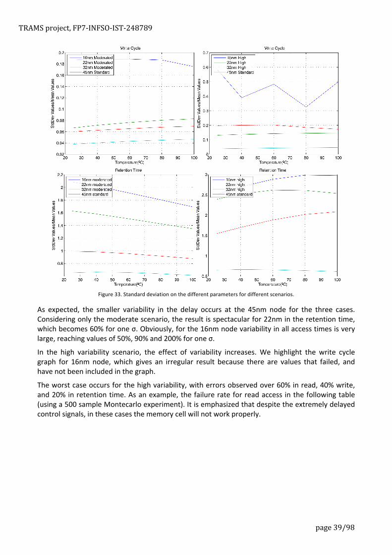
TRAMS project, FP7-‐INFSO-‐IST-‐248789
page 39/98
Figure 33. Standard deviation on the different parameters for different scenarios.
As expected, the smaller variability in the delay occurs at the 45nm node for the three cases. Considering only the moderate scenario, the result is spectacular for 22nm in the retention time, which becomes 60% for one σ. Obviously, for the 16nm node variability in all access times is very large, reaching values of 50%, 90% and 200% for one σ.
In the high variability scenario, the effect of variability increases. We highlight the write cycle graph for 16nm node, which gives an irregular result because there are values that failed, and have not been included in the graph.
The worst case occurs for the high variability, with errors observed over 60% in read, 40% write, and 20% in retention time. As an example, the failure rate for read access in the following table (using a 500 sample Montecarlo experiment). It is emphasized that despite the extremely delayed control signals, in these cases the memory cell will not work properly.

TRAMS project, FP7-‐INFSO-‐IST-‐248789
page 40/98
Temp. (ºC) 45nm 32nm 22nm 16nm
standard moderated high moderated high very high moderated high very
high
25 0 % 0 % 0.2 % 0 % 0.4
% 24.4 % 1.4 % 13.6
% 56.4 %
40 0 % 0 % 0.2 % 0 % 0.4
% 25.2 % 1.4 % 14.4
% 57.6 %
60 0 % 0 % 0.2 % 0 % 0.4
% 26.8 % 1.6 % 14.8
% 59.2 %
80 0 % 0 % 0.2 % 0 % 1 % 26.4
% 1.4 % 15.4 % 60.2 %
100 0 % 0 % 0.2 % 0 % 0.8
% 27 % 1.6 % 15.8 % 61.4 %
Table 6. Failure rate for read access
5.1.6. Effects of Voltage variation The measurement of voltage variation has been made without including the process variation. It has been considered a +/-‐10% effect due to RI and LdI/dt drops. The following figures show the results for the four nodes, also depending on the temperature. The nominal voltage for the 45nm node, 32nm, 22nm and 16 nm are: 1 volts, 0.9 volts, 0.9 volts and 0.7 volts, respectively.
20
4060
80100
120
0.91
1.11.2
1.32
2.5
3
3.5
4
4.5
5
x 10-10
Temper
Read Cycle 45 nm
VDD20
4060
80100
120
0.80.85
0.90.95
1
3
3.5
4
4.5
5
5.5
6
x 10-10
Temper
Read Cycle 32 nm
VDD
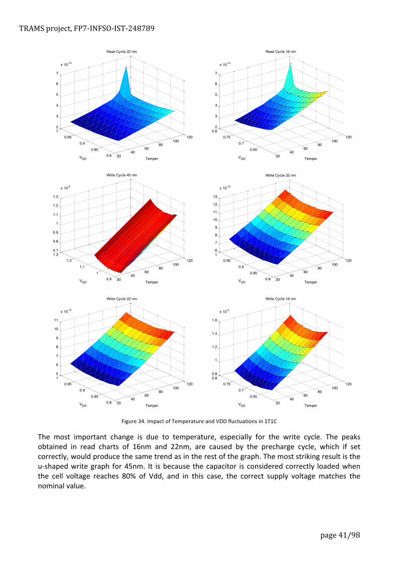
TRAMS project, FP7-‐INFSO-‐IST-‐248789
page 41/98
Figure 34. Impact of Temperature and VDD fluctuations in 1T1C
The most important change is due to temperature, especially for the write cycle. The peaks obtained in read charts of 16nm and 22nm, are caused by the precharge cycle, which if set correctly, would produce the same trend as in the rest of the graph. The most striking result is the u-‐shaped write graph for 45nm. It is because the capacitor is considered correctly loaded when the cell voltage reaches 80% of Vdd, and in this case, the correct supply voltage matches the nominal value.
2040
6080
100120
0.80.85
0.90.95
12
3
4
5
6
7
x 10-10
Temper
Read Cycle 22 nm
VDD20
4060
80100
120
0.650.7
0.750.8
2
3
4
5
6
7
x 10-10
Temper
Read Cycle 16 nm
VDD
2040
6080
100120
0.91
1.11.2
1.30.7
0.8
0.9
1
1.1
1.2
1.3
x 10-9
Temper
Write Cycle 45 nm
VDD20
4060
80100
120
0.80.85
0.90.95
16
7
8
9
10
11
12
13
x 10-10
Temper
Write Cycle 32 nm
VDD
2040
6080
100120
0.80.85
0.90.95
15
6
7
8
9
10
11
x 10-10
Temper
Write Cycle 22 nm
VDD20
4060
80100
120
0.650.7
0.750.80.8
1
1.2
1.4
1.6
x 10-9
Temper
Write Cycle 16 nm
VDD

TRAMS project, FP7-‐INFSO-‐IST-‐248789
page 42/98
5.1.7. Conclusions The effects of PVT on foreseeable future technologies on 1T1C cell have been investigated. As MOS device models PTM have been used. Finally the global effects are presented.
The next graphs summarize the results. In all of them the additional delays (in percentage) for the write and read cycles induced by the PVT effects have been shown. It has also been included as reference, the nominal value. Both scenarios, moderated and high, are drawn in different charts, but the scenario “very high” has not been drawn due to the high failure rate. In Figure 37 the worst case has been drawn for temperature, process and voltage variability, but as process and voltage variability have low dependence on temperature in read/write cycles (see Figure 33), it can be used as upper limit.
In the worst case, for a 16nm technology and a moderate scenario, the delay in the write cycle increases by 155%. The case of read cycle is worse, for the same technology, surprisingly increased by 500%, and only in the moderated scenario.
Figure 35. PVT effects on Write cycle for moderate scenario
Figure 36. PVT effects on Write cycle for moderate scenario
0 50 100 150 200 250
45nm
32nm
22nm
16nm
PVT effects on Write for moderated scenario
Nominal
Temperature
Process
Vdd
0 50 100 150 200 250 300 350 400
45nm
32nm
22nm
16nm
PVT effects on Write for high scenario
Nominal
Temperature
Process
Vdd

TRAMS project, FP7-‐INFSO-‐IST-‐248789
page 43/98
Figure 37. PVT effects on Read cycle for moderate scenario
Figure 38. PVT effects on Read cycle for high variability scenario
The effects on the retention time have not been included, but the retention time variation could get to changes of 197%, 297%, 488% and 626% for 45nm, 32nm, 22nm and 16nm, respectively.
If we consider the "very high" scenario, the failure rate grows up to 26% for 22nm, and 59% for 16nm in the read cycle. Clearly, this failure rate is not acceptable.
0 200 400 600 800
45nm
32nm
22nm
16nm
PVT effects on Read for moderated scenario
Nominal
Temperature
Process
Vdd
0 100 200 300 400 500 600 700 800
45nm
32nm
22nm
16nm
PVT effects on Read for high scenario
Nominal
Temperature
Process
Vdd

TRAMS project, FP7-‐INFSO-‐IST-‐248789
page 44/98
5.2. Introduction to the 3T1D DRAM cell The 3T1D cell was proposed by Luk and Dennard (IBM) in 2005 [2] [37], as a promising DRAM memory, compatible with conventional CMOS technologies. In fact an original evolution of the earlier version of the 3T cell was presented by Intel in 1970 [38].
Figure 39. Schematic of the 3T1D DRAM cell.
In the case of the 3T1D the specific storage capacitor of 3T is substituted with a MOS capacitance incorporated as gated-‐diode. Figure 39 shows the scheme of this basic cell. The basis of the storage system is the charge placed in node S, written from BLwrite line when T1 is activated. Consequently it has a dynamic nature, but allows a non-‐destructive read process (an advantage in comparison with 1T1C) and high performance read and write operations, comparable with 6T. Because the whole cell has only 4 NMOS transistors (T1 and T3 work as accessing devices), in comparison with 6T with 6 transistors, the area of a 3T1D is around 40% lower than the corresponding for the 6T with equivalent performances, so 3T1D is more compact. In order to write the cell at the BLwrite line level it is only required to activate T1 through the word line write WL-‐write. Hence, the S node stores a 0 voltage or a VDD-‐VTH voltage depending on the logic value. The voltage value is stored on the D1 and T2 gate capacitances.
In order to read the cell, the read bitline BLread has to be previously precharged at VDD level. Then T3 is activated from WLread line. From a 1 (high) level stored in S, transistor T2 turns on and discharges the bitline. If a 0 (low) level is stored in S, transistor T2 does not reach enough conduction level. The objective of the gated diode D1 is to improve access time. When a 1 (high) level is stored in S, D1 connected to WLread line causes a boosting effect on the voltage level in node S. This voltage is close to VDD voltage causing a fast discharge of the parasitic capacitance in BLread.
5.3. Modelling and analysis of access and retention time of a 3T1D 32kB cache memory including technology nodes and temperature variations.
This section analyses the impact of temperature, voltage and technology node for 45, 32, 22 and 16 PTM CMOS technologies and 18 and 13 nm from WP1 on a 32KB L1 cache complete memory

TRAMS project, FP7-‐INFSO-‐IST-‐248789
page 45/98
system, in parallel to what was done in Section 4.1 with the 6T cell. The cache structure is the one presented in 4.1 where all the signals controlling the basic cell are compatible, with the only difference that in read operation the sense amplification procedure is of single-‐ended type for the 3T1D, in comparison with the differential technique in the 6T. No process variations are considered in this section.
Hspice simulations at different temperatures (30, 50, 70, 90 and 110 oC), with nominal parameter MOS devices for 45, 32,22 and 16 (PTM, @0.9volt) and 18 and 13 (WP1, @0.7volts), have been performed for 3T1D 32KB L1 cache memory. Table 7 shows the numeric results for Read_Access, Write_Access and Retention time. Both access times increases with temperature with an average increase of a 60% from 30 to 100 oC, the slope of this increase augments with the technology shrinking and access times decreases with it.
Retention time decreases abruptly with temperature due to the increase of leakage currents, about 10X for the same temperature margin. The technology shrinking also affects severely the retention time, caused by the corresponding increase of leakage currents. For the 18 nm and 13 nm technologies, retention time decreases about 100 times respect to 16nm, the reason is that those two technologies have a higher sub threshold current level (the threshold voltage for PTM technologies is around 450 mV while in the case of 18 and 13 nm is close to 200 mV. Figure 40, Figure 41 and Figure 42 display these results.
Read_Access_Time (ns) Write_Access_Time (ns) Retention time (ms) Tecno/
Temperature 30 50 70 90 110 30 50 70 90 110 30 50 70 90 110
45nm PTM 2.1 2.6 3.0 3.2 3.5 2.0 2.6 2.9 3.0 3.3 64 35 21 19 10
32nm PTM 1.8 2.3 2.7 3.1 3.5 1.7 2.2 2.4 3.0 3.3 28 20 14 10 6
22nm PTM 1.6 1.9 2.3 2.7 2.9 1.6 1.7 2.1 2.5 2.6 21 14 9 5.5 3
16nm PTM 1.4 1.7 2.0 2.3 2.6 1.4 1.5 1.9 2.1 2.2 11 8.4 5.1 2.3 1.9
18nm WP1 0.9 1.2 1.8 2.0 2.3 1.0 1.2 1.8 2.1 2.4 0.1 0.09 0.08 0.05 0.01
13nm WP1 0.8 1.1 1.6 1.9 2.1 0.9 1.1 1.4 2.0 2.1 0.09 0.07 0.06 0.03 0.007
Table 7. Results of 3T1D 32KB cache for different technology processes and temperatures. No process variation is considered. Observe that 18 and 13 nm (WP1) technologies are HP (high performance) devices while PTM are LP (low power).

TRAMS project, FP7-‐INFSO-‐IST-‐248789
page 46/98
Figure 40. Impact of temperature in 3T1D 32KB cache for PTM technologies on access and retention time
Figure 41. Impact of PTM technologies in Access and Retention time

TRAMS project, FP7-‐INFSO-‐IST-‐248789
page 47/98
Figure 42. Comparison of read_access time and retention time for 16nm PTM and 18nm WP1 technologies
5.3.1. Conclusions
The read and write cycle times for the 3T1D is very close to the times for the 6T SRAM, with a 40% of silicon area reduction, and lower consumption. The impact of temperature on those times is also similar to the obtained for the 6T (around a 60% of increase from 15 to 110 oC). Charge retention time is a key factor in dynamic RAMs. For the small size of the 3T1D the retention time is much lower that the calculated in the 1T1C case (100 times lower), and as it happened in the case of the 1T1C the retention time is very sensitive to temperature with drastic reductions in the temperature margin considered.

TRAMS project, FP7-‐INFSO-‐IST-‐248789
page 48/98
5.4. Robustness analysis of the 3T1D cell In this section we proceed with the analysis of the robustness of 3T1D following a method parallel to the one presented in section 4.2. The objective is to determine the Satisfiability Boundary for a variation map of threshold voltages of the four transistors that constitute the basic 3T1D cell (T1, D1, T2 and T3, see Figure 39). In this section only a 2D map has been considered, so for each of the three basic operations the two more significant transistors are considered. The rest of parameters are considered nominal.
Read operation
In this operation only transistor T2 and D1 has been considered with variable threshold voltage.
Write operation
Transistor T1 and D1 are considered in the write analysis.
Hold or Retention operation
In this operation only transistor T2 and D1 has been considered with variable threshold voltage.
The analysis has been done in each case with incremental values of the threshold voltage (0.05 volts per step) for both devices independently, following 4 lines (vertical and horizontal, only one voltage varies and the two 45o and 135o lines). Each point has been simulated determining if the point verifies or not the acceptable condition generating a first approach to the acceptance region. Table 8 shows the results obtained with the 3T1D.
Assuming Gaussian independent distribution for the two variables the two-‐dimensional independent distributions are integrated inside the acceptance region (Matlab).
Model Tech. Vth
Varia-‐ bility
Retention (PRE) T <0.2 nominal
Write (PFW) Twrite>2nominal
Read (PR) Tread>2nominal Cell (failure
PCELL)
Yield(%) 32k
PTM
45nm 4% 0 0 0 0 100
32nm 6% 0 0 0 0 100 15% 8.0e-‐8 3.0e-‐8 4.0e-‐8 5.0e-‐8 99.84
22nm 8% 4.0e-‐7 1.0e-‐8 8.0e-‐8 1.0e-‐8 99.96 15% 1.0e-‐7 3.0e-‐7 1.0e-‐7 2.0e-‐7 99.36 30% 1.25e-‐5 2.0e-‐6 3.2e-‐6 8.0e-‐6 77.41
16nm 10% 2e-‐8 6e-‐7 1.6e-‐7 2.21e-‐7 99.36 20% 1e-‐6 2.0e-‐6 1.21e-‐7 9.0e-‐7 97.16 40% 3e-‐4 2.9e-‐4 6.4e-‐5 1.0e-‐4 4.07
WP1
18 nm 58% 3.0e-‐4 1e-‐4 4.0e-‐5 1.42e-‐4 1.13 13 nm 58% 1.0e-‐3 1e-‐3 3.0e-‐4 9.0e-‐4 0
Table 8. Failure probability for different technologies and variability scenario for the 3T1D cell. This analysis has been done for minimum size devices (W/L=1), so the results are an overestimation of sized cell.
Very high variability scenario represents yield near 0% for WP1 technologies, 4% for 16nm and 77.41% for 22nm. For moderate variability 3T1D exhibits an acceptable yield. In general the failure probability of 3T1D is lower than the one with 6T, and consequently presents a higher yield.

TRAMS project, FP7-‐INFSO-‐IST-‐248789
page 49/98
5.4.1. Conclusions Following a parallelism with the SB technique explained in 4.2 for the 6T the robustness of the 3T1D has been analysed. Only two devices variation analysis has been performed for each of the three time cycles (write, read and retention times). The results are similar to the ones presented for the 6T. Although in the case of the 3T1D a higher robustness has been shown compared to 6T, showing low but acceptable yields for high variability scenario in 22 and 16 (where in the case of 6T we found negligible yield). The yield obtained for very high variability for 22, 16, 18 and 13 nm, is practically zero.
5.5. Reliability aspects for 3T1D DRAM cells 5.5.1. Introduction System reliability is arising as a major concern in next-‐generation designs and implementations of memory systems. The situation is aggravated in the case of small transistors to minimize area, such as the ones used in 6T SRAM and 3T1D DRAM cells. Higher variation of characteristic parameters like threshold voltage leads to less predictable devices. Random behaviour requires larger guard bands to satisfy the requirements of reliability. This trend compromises the gain in performance expected for new technology generations.
Reviewing the literature we can find many papers on the reliability issues of 6T SRAM cells. In a work from S. Mukhopadhyay [39] the failure probabilities associated to access-‐time, read/write failure and hold failure in 6T SRAMs are analysed and modelled against process-‐parameter variations. In the work from M. Meterelliyoz [16] thermal studies of 6T and 8T SRAMs cache memories are performed and the stability, noise immunity and performance parameters are extracted and analysed. There are also studies on the effects of NBTI in 6T SRAMS like the paper from K. Kang [40]. However, despite the abundance of works for 6T, there are few articles on 3T1D. In this subsection we review an unexplored reliability problem of 3T1D cell. We analyse the effects of the aging of 3T1D cell due to Positive Bias Temperature Instability (PBTI). PBTI aging mechanism has not received much attention so far due to its relative small impact with respect to other ways of aging. However, since the introduction of high-‐k dielectrics, PBTI is growing in importance and it is expected to dominate NMOS aging in future technology nodes [41] [42] [43]. We end the subsection with a comparison between 6T and 3T1D cell.
Since the first proposal of 3T1D cell, from W. Luk et al. [37], this new memory cell is being carefully investigated in order to explore its capabilities and precisely compare them with 6T. In the paper from K. Lovin et al. [44] a performance model is developed to study 3T1D memories with accurate results and fast simulations. 3T1D cell does not have a symmetrical structure like 6T cell. For this reason, the problems related to instability and bit flipping, usual in 6T cells, do not affect 3T1D. All possible variations in device behaviour on a 3T1D cell can be lumped into variations of data retention times. In this sense, 3T1D is more robust against variability than 6T cell. In the literature we can find specific comparison between these two main candidates for data caches memories. In the paper from X. Liang et al. [45] different schemes for the L1 data cache are analysed under different levels of variation. They obtain that 6T memories suffer 40% reduction in frequency when variability is severe while 3T1D cell loses only 4% of performance with the same level of variability.
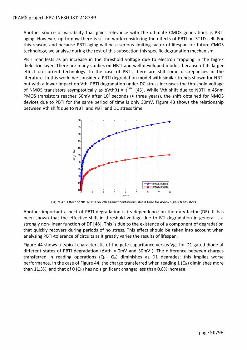
TRAMS project, FP7-‐INFSO-‐IST-‐248789
page 50/98
Another source of variability that gains relevance with the ultimate CMOS generations is PBTI aging. However, up to now there is sill no work considering the effects of PBTI on 3T1D cell. For this reason, and because PBTI aging will be a serious limiting factor of lifespan for future CMOS technology, we analyse during the rest of this subsection this specific degradation mechanism.
PBTI manifests as an increase in the threshold voltage due to electron trapping in the high-‐k dielectric layer. There are many studies on NBTI and well-‐developed models because of its larger effect on current technology. In the case of PBTI, there are still some discrepancies in the literature. In this work, we consider a PBTI degradation model with similar trends shown for NBTI but with a lower impact on Vth. PBTI degradation under DC stress increases the threshold voltage of NMOS transistors asymptotically as ∆Vth(t) ∝ t1/6 [43]. While Vth shift due to NBTI in 45nm PMOS transistors reaches 50mV after 108 seconds (≈ three years), the shift obtained for NMOS devices due to PBTI for the same period of time is only 30mV. Figure 43 shows the relationship between Vth shift due to NBTI and PBTI and DC stress time.
Figure 43. Effect of NBTI/PBTI on Vth against continuous stress time for 45nm high-‐k transistors
Another important aspect of PBTI degradation is its dependence on the duty-‐factor (DF). It has been shown that the effective shift in threshold voltage due to BTI degradation in general is a strongly non-‐linear function of DF [46]. This is due to the existence of a component of degradation that quickly recovers during periods of no stress. This effect should be taken into account when analysing PBTI-‐tolerance of circuits as it greatly varies the results of lifespan.
Figure 44 shows a typical characteristic of the gate capacitance versus Vgs for D1 gated diode at different states of PBTI degradation (∆Vth = 0mV and 30mV ). The difference between charges transferred in reading operations (Q1− Q0) diminishes as D1 degrades; this implies worse performance. In the case of Figure 44, the charge transferred when reading 1 (Q1) diminishes more than 11.3%, and that of 0 (Q0) has no significant change: less than 0.8% increase.
0 1 2 3 4 5 6 7 810
15
20
25
30
35
40
45
50
55
60
years
|V th
| (m
V)
pMOS (NBTI)nMOS (PBTI)

TRAMS project, FP7-‐INFSO-‐IST-‐248789
page 51/98
Figure 44 Gated-‐diode capacitance Cgs versus Vgs with and without 30mV of Vth shift due to PBTI degradation
5.5.2. Objectives Our goal is to analyse the main trends of 3T1D degradation due to PBTI and see the potential impact of this aging mechanism in the reliability of the memory cell. In order to perform this study, we first define a fault model based on critical parameters. Then, analysing the performance of the 3T1D cell by means of these critical parameters, we are able to evaluate the robustness of the 3T1D cell against PBTI degradation. Among all possible modes of operation of a memory cell we identify as the most critical both hold and read. Timing condition for write operation is not as critical as for read. Read operation requires charging or discharging an entire BLread line and it has an equivalent capacitor bigger than the equivalent parallel D1 and T1 capacitances of a single 3T1D cell. In hold mode, we have to consider the leakage that will discharge continuously the accumulated charge in the node S. Let us note here, before starting with the critical parameter definitions, that critical situations for both hold and read operations occur only when the data stored in the cell corresponds to high level (1). Otherwise, no leakage will discharge node S and no timing problem will affect our reading, as BLread does not discharge.
-‐ Hold Operation:
When a bit is stored in a 3T1D cell, both T1 and T3 access transistors are switched off. In these conditions there is a subthreshold leakage flowing from node S through T1 and a smaller current of gate leakage flowing through T2 and D1. As a consequence, node S discharges over time as long as no other write or refresh operation is performed. After a certain time, when the voltage in node S decreases under a certain level VSmin, data in node S is lost because it cannot be read within the slot time available according to the operating clock frequency.
A proper way to quantify how critical is the hold operation is to measure the time needed to discharge the node S from the nominal value Vdd−Vth, achieved after a writing or refresh operation, to VSmin, the moment when data is lost.
-‐ Read Operation:
When reading, T3 transistor is activated and BLread is connected through T2 to the ground. Diode D1 receives a pulse as WLread is activated and the boosting effect activates T2, which starts to
0.4 0.2 0 0.2 0.4 0.6 0.8 1 1.2 1.40.05
0.1
0.15
0.2
0.25
0.3
Q1Q0
Vgs (V)
Cap
acita
nce
(fF)
not degradeddegraded ( Vth = 30mV)

TRAMS project, FP7-‐INFSO-‐IST-‐248789
page 52/98
discharge BLread line. The time needed to get access to the data depends directly on how fast BLread discharges.
We define the read access time as the time needed to discharge 20% of BLread line given an initial nominal charge Vdd. We consider this level of voltage drop enough to activate the sense amplifier.
5.5.3. Retention and Read Access time Analysis Here we present the analysis results of 3T1D-‐DRAM cell’s critical parameters VSmin, retention time and read access time against PBTI degradation effects. Results are derived from HSPICE electrical simulations using 45nm PTM device models (only 45nm has been included in this deliverable from brevity reason). We perform the measurements at three different temperatures (25 oC, 60 oC and 100 oC) and three different source voltages (the nominal value Vdd and the corners of ±10%) in order to get an idea of the effect of environmental variations. The modelling of PBTI in HSPICE, as a Vth shift, is performed by adding a DC voltage source (∆Vth) in series with the gate terminal of the transistor. Nominal values to model the cell at 45nm are extracted from the work by K. Lovin et al. [44].
5.5.3.1 VSmin Characterization Before starting with the retention time analysis we need to characterize the VSmin value for different environmental conditions. VSmin highly depends on the working temperature as it affects directly the amount of leakage current. Figure 45 depicts the read access times of a 3T1D cell against different initial charges in node S. Read access times are computed according to the previous definition and for a cell working at different temperatures. The VSmin parameter can be found at each temperature as the voltage in node S with exactly the same read access time as the available slot time fixed by the clock frequency. In this paper we will consider an operating frequency of 3.5GHz, then, adding the corresponding guard bands, we have as a requirement the maximum admissible read access time taccess ≤ 250ps.
Figure 45 Read access times against voltage in node S of 3T1D cell working at different temperatures (VSmin condition in slashed
line)
0.4 0.42 0.44 0.46 0.48 0.5 0.52 0.540
50
100
150
200
250
300
350
400
Acce
ss ti
me
(ps)
V(S)
access time for 3.5GHzaccess time at T=25oCaccess time at T=60oCaccess time at T=100oC
Vdd Vth

TRAMS project, FP7-‐INFSO-‐IST-‐248789
page 53/98
We observe in Figure 45, apart from the negative impact of reducing the voltage in node S, that variations in working temperature cause a small and quite stable effect on the read access time through all charges considered in node S. Actually, any variation of temperature within the range of 60 oC to 100 oC implies a variation in the read access time of about 0.4ps/oC, given a 3T1D cell with the nominal charge Vdd−Vth.
5.5.3.2 Retention time Using the previous definition of retention time and the VSmin parameter characterization, we perform simulations of 3T1D cell at different temperatures and different states of PBTI degradation (∆Vth). We assume the same degradation for both D1 and T2 transistors because they share the same gate to source voltage Vgs with only small differences during short periods of time (reading operations). T1 degradation occurs only scarcely and during a short period of time (writing operations of low value (0)). Moreover, it has no effect on read access time and a positive effect in retention time as it reduces the leakage current. Figure 46 shows the resulting retention times when considering different states of PBTI degradation (∆Vth). It is clear that a temperature increase implies significant reduction in the retention time. For example: increasing temperature from 60 oC to 100 oC implies about halving the retention time in any case.
Figure 46 Impact of PBTI on retention times at different working temperatures. Error bars correspond to ±σ voltage variations
(3σ=10%Vdd)
Another relationship detected in Figure 46 is that at temperatures above 60 oC the effect of PBTI degradation becomes irrelevant. Only for values of temperature under 60 oC PBTI has a significant positive effect on the retention time. For example: at 25ºC, an increase in the threshold voltage ∆Vth of 30mV implies about 7.6% increase in the retention time. From these results we can conclude that refreshing techniques in 3T1D-‐DRAM memories do not need to take into account the effects of PBTI because they are negligible at high temperatures and positive at lower temperatures.
5.5.3.3 Read Access Time The time required to access the data in a cell depends a lot on the amount of charge remaining in the node S (see Figure 47). Depending on the time between refreshing operations we will have different probabilistic distributions of voltage in node S. We represent in the following simulation,
0 5 10 15 20 25 30 35 40 45 500
2
4
6
8
10
12
Ret
entio
n tim
e (!
s)
Vth (mV)
T=25o CT=60o CT=100o C

TRAMS project, FP7-‐INFSO-‐IST-‐248789
page 54/98
in Figure 47, the read access times of a 3T1D cell at different temperatures against different states of PBTI degradation.
Figure 47 Impact of PBTI on read access time at different working temperatures. Error bars correspond to ±σ voltage variations
(3σ=10%Vdd)
We can see in this case a significant negative impact of PBTI on 3T1D performance. Read access time significantly increases with small Vth shifts. From the above results we obtain that a Vth increase of 30mV implies a 26% increase in read access time of a 3T1D cell working at 60ºC. As a final observation in this subsection, we see that PBTI should be taken into account when studying the timing conditions of memory cells with small NMOS transistors, especially after the introduction of high-‐k dielectrics.
5.5.4. Yield Consideration Here we present a study on the manufacturing yield of 2kB cache memory blocks compounded of 3T1D memory cells. We assume a reconfigurable structure with 32 cells per column, 512 columns and 24 redundant columns. Taking into account all possible sources of variability (process, voltage, temperature and aging) we perform 10,000 Monte Carlo simulations. Figure 48 shows the yield of this memory against the level of PBTI degradation at three different temperatures.
Figure 48 Yield of 2kB 3T1D memory blocks
0 5 10 15 20 25 30 35 40 45 5060
80
100
120
140
160
180
200
220
240
Acce
ss ti
me
(ps)
Vth (mV)
access time at T=25oCaccess time at T=60oCaccess time at T=100oC
0 5 10 15 20 25 30 35 40 45 500
0.1
0.2
0.3
0.4
0.5
0.6
0.7
0.8
0.9
1
Vth (mV)
Yiel
d
Yield of 2kB 3T1D memory blocks
90% yieldT=25o CT=60o CT=100o C

TRAMS project, FP7-‐INFSO-‐IST-‐248789
page 55/98
The basis for regarding a cell as defective is to check if the read access time holds the requirement presented previously: taccess ≤ 250ps. From the figure we see how important is the temperature combined with PBTI degradation. If we need a 90% yield in our manufacturing process, we cannot admit more than 22mV, 33mV and 43mV of Vth shift when working at 100 oC, 60 oC and 25 oC respectively.
Regarding the relationship between Vth shift and stress time presented in Figure 43, the above result allows us to make a rough prediction of the lifespan of our simulated 2kB memory blocks. When doing so, it has to be considered the particular application of our circuit because the relationship between Vth shift and stress time presented highly depends on the duty-‐factor. When there are periods with no stress, the effects of relaxation significantly vary the relation between Vth shift and time. In the particular case of 3T1D cells used in L1 cache memory, the storage of high (1) logic values, the ones that produce PBTI degradation in T2 and D1, statistically occur only half of the time.
5.5.5. Comparisons and partial conclusions Contrasting the above results for yield of 2KB 3T1D memory blocks and a previous work on 6Ts from S. Drapatz et al. [47], we observe that the impact of PBTI in both memory structures is relevant and within the same order of magnitude.
Figure 49 Yield including global and local variations after long hold of one data with NBTI and PBTI degradation for a single Bit cell
(Extracted from [47]).
Figure 49 depicts the yield for the hold operation of a 6T cell against different supply voltages and different levels of NBTI-‐PBTI degradation. The increase in the threshold voltage with BTI drives the 6T cell structure to a less stable point and it becomes less reliable. 6T SRAM yield decreases quickly when the effect of PBTI increases. In the referred study, the authors conclude that the combination of PBTI with NBTI is much worse for 6T SRAM reliability than considering only NBTI. During hold state the two effects are adding, so that the cell weakens drastically in terms of read stability.
We conclude from the previous yield considerations of both 3T1D and 6T cells that PBTI degradation mechanism should not be ignored in memory system designs. In order to be able to produce long-‐life memory structures it is very important to consider the effects of PBTI and NBTI. The combination of these aging mechanisms with other sources of variability gradually weakens the robustness and the reliability of memory systems at specific conditions of usage for both 6T SRAM and 3T1D DRAM memory cells.

TRAMS project, FP7-‐INFSO-‐IST-‐248789
page 56/98
6. Impact of process variation on memory systems, evaluation of cache memories with 6T and 3T1D cells.
In this section the impact of the process variations on the 32KB L1 cache system performances is analysed. The structure of the memory is the one described in Section 4, and used also in Section 5. The variability scenario is the model described in Table 1 (section 3) for technologies of 32, 22 and 16 nm, modelled with PTM, and the model in Table 2 for 18 and 13 nm which models are results of WP1.
6.1. The analysis The analysis has been performed with Hspice, applying systematic geometric variations and threshold voltage systematic and random (as stated in the variability model). Analysis has been performed at three temperatures, 25, 60 and 100 oC. Power supply voltage is the nominal in all the simulations (0.9 volts for 32,22,16nm and 0.7 volts for 18,13nm).
Technology Temperature
Scenario
25 C
(%)
60 C
(%)
100 C
(%)
6T 3T1D 6T 3T1D 6T 3T1D
45 nm Standard 3 3 3.2 3.1 3.5 3.5
32 nm Moderate 3.5 3.4 3.8 3.75 4 3.95
High 10 9 15 12 21 20
22 nm Moderate 4.5 4 5 4.2 6 5
High 11 10 16 15 23 21
Very high 18
(0.5)
16
(0.0)
26
(1.0)
23
(0.2)
35
(2.0)
32
(0.4)
16 nm Moderate 5.2 4.1 6.2 5.4 7 6.5
High 15
(0.4)
14
(0.0)
17.5
(0.5)
16
(0.0)
26
(1.5)
23.5
(0.3)
Very High 21
(1.0)
20
(0.4)
31
(2.0)
26
(0.5)
40
(2.8)
34
(0.7)
18 nm WP1 25
(1.0)
X 34
(2.5)
X 45
(3.3)
X
13 nm WP1 25
(1.5)
X 35
(2.8)
X 47
(3.7)
X
Table 9. Write-‐Read cycle variations for 32KB with 6T and 3T1D and different technologies and scenarios. Number into brackets means percentage of write-‐read failures.

TRAMS project, FP7-‐INFSO-‐IST-‐248789
page 57/98
Table 9 shows the percentage of the sigma write-‐read cycle time for 1000 Montecarlo samples (half of them writing a 1 and half a 0). For high and very high scenarios a bold number is indicated between parentheses, which indicates the percentage of the cases where the write-‐read failed (bit flip in the case of a 6T or a failure in 3T1D). For 6T the failures are approximately equi-‐probable while in the case of 3T1D only flips from 0 to 1 appear, due to the characteristic of the cell. Figure 50 and Figure 51 show graphically the write-‐read access time standard deviation for high and very high variability scenarios. Variability increases substantially with temperature and the variation is higher for 6T but with the same order.
Figure 50. Standard deviation for access time in cache memory for different technologies and high variability scenario.

TRAMS project, FP7-‐INFSO-‐IST-‐248789
page 58/98
Figure 51. Standard deviation for access time in cache memory for different technologies and very high variability scenario.
Figure 52. Percentage of write-‐read failures caused by process variation.
Finally Figure 52 shows the percentage of failures observed in the experiment. All these failures correspond to an incorrect writing-‐read cycle (a 1 is written but a 0 is read and vice versa). For moderate variability there is no error, but there are several for high and very high variability levels. Observe that for the worst case (6T 13nm 100 oC) the percentage of failure cycles is 3.8%, which is an unacceptable value for reliable memories. 3T1D memories appear more tolerant to variations (in the case of failures): this is due to the characteristics of the cell. The 6T cell is more sensitive because of the balance requirement in the transistor of the cell; this fact does not apply for the dynamic cell. Additionally in the case of the 3T1D only single transition failures are observable due to the single end pre-‐charged bit read line.
The experiment shows that process variability not only affects the speed performances of memories, but also affects the reliability of the memory in a very substantial level.
6.2. Conclusions At cache level we have analysed the variability on the write-‐read cycle for both 6T and 3T1D. As the robustness analysis at bit-‐cell level already shown the impact of variability on the performances of the cache circuit are drastic. The 3T1D shows a lower impact, in comparison with 6T, but for both of them we find also catastrophic faults in the write-‐read cycle. As we concluded in previous section, with this percentage of catastrophic faults the yield expected at cache level is practically zero for the very high variability scenario in 22 and 16 nm as well as in the case of 18 and 13nm technologies investigated in TRAMS WP1.

TRAMS project, FP7-‐INFSO-‐IST-‐248789
page 59/98
7. Robustness of memory cells in front of SEU: SRAM Reducing leakage power and improving the reliability of data stored in the memory cells are both becoming challenging as technology scales down. While the smaller threshold voltages causes increased leakage, smaller supply voltages and node capacitances can be a problem for soft errors. In modern processors SRAMs occupy more than 50% of the chip area. Hence it is more likely that the single-‐event upset (SEU) occur in the SRAMs. It is crucial to guarantee the reliability of the SRAM cells as the technology scales down.
The objective of this work is to carry out a detailed analysis of the scaling trends of the soft error problem for the traditional 6T SRAM memory cell for different level of voltages and for different process nodes.
7.1. Introduction Due to current technology scaling trends, digital designs are becoming more susceptible to radiation induced particle hits resulting from radioactive decay and cosmic rays, than all other factors [48]. A low energy particle that before had no effect on a circuit can now flip the output of a gate. Such a bit-‐flip of a gate is called a single-‐event transient (SET) or a glitch. A single-‐event upset (SEU) or a soft error occurs if the SET is propagated to an output and latched into a memory element. These failures are called soft errors because they do not permanently damage the circuit but do destroy data.
The rate at which soft errors occur is referred to as soft error rate (SER). The level of soft error vulnerability is important since it directly influences the error detection and the correction mechanisms employed in the circuitry.
Soft errors are caused by two types of radiation alpha particles emitted by radioactive impurities in IC and package materials and high-‐energy neutrons resulting from the interaction of cosmic radiation with the earth’s atmosphere [49]. Moreover, the soft error rate is inherently related to the device parameters (e.g., L and Vth).
The report is organized in the following sections. We first provide a brief introduction to the soft error problem and the study of the state of the art. It is followed by the discussion of the simulation platform and the particle strike modelling and the injection of the soft-‐errors. Finally the results and concluding remarks are given.

TRAMS project, FP7-‐INFSO-‐IST-‐248789
page 60/98
7.2. Soft error: Background and state of the art
Figure 53 Traditional 6T SRAM cell.
As shown in Figure 53, the 6T SRAM memory cell has two sensitive nodes, the drain of the OFF-‐NMOS transistor and the drain of the OFF-‐PMOS transistor, ! and ! respectively as shown in the figure. The drain and substrate of the OFF transistor create a reverse-‐biased junction. The reverse-‐biased junctions of the cell are most sensitive nodes to the particle strikes.
Let us assume that a particle hits our silicon. Immediately followed by the particle strike, charges generation and collection occur. The generated charges are collected at the opposite voltage terminals of the reverse-‐biased. The movements of charges cause a current pulse at the struck node. The memory cell flips when the collected charge, Q, is more than the charge stored at the struck node.
A method for estimating SER in CMOS SRAM circuits was recently developed by [50]. This model estimates SER due to atmospheric neutrons (neutrons with energies >1MeV) for a range of submicron feature sizes. It is based on a verified empirical model for the 600nm technology, which is then scaled to other technology generations. The basic form of this model is:
!"# ! !!"#$ .!!"## . !"#!!"#$
!!"!! Equation 16
As it is evident from the equation, SER sensitivity of SRAMs depends on: (i) the critical charge Qcrit, which is the minimum amount of charge that needs to be injected into the critical node in order to flip the state of the memory, (ii) the diffusion area (Adiff) of the sensitive drain, which implies that the probability of a soft-‐error is linearly related to the probability that an alpha-‐particle hits the sensitive drain area, (iii) the charge collection efficiency (Ccoll), which is a measure for the amount of deposited charge that a circuit node collects after an alpha-‐particle impact and is a constant for the given technology and the device, and (iv) Nflux , which is the neutron flux with the energy >1MeV.
From equation 16, it is obvious that changes in the value of Qcrit relative to Ccoll will have a very large impact on the resulting SER. The SER also decreases proportional to the square of the device size. Hazucha & Svensson [50] used this model to evaluate the effect of device scaling on the SER of memory circuits. They concluded that SER-‐per-‐chip of SRAM circuits should increase at most linearly with decreasing feature sizes.
Because Qcrit is directly related to the soft-‐error rate, understanding the effects of the factors affecting Qcrit is important to estimate the SER of a circuit. The higher the Qcrit the more robust the circuit is.

TRAMS project, FP7-‐INFSO-‐IST-‐248789
page 61/98
Figure 54 Various contributions to the error rate for a small area SRAM cell, designed with 350nm CMOS cell vs. Critical Charge
Figure 54 shows how various contributions to the terrestrial error rate are affected by critical charge [51] . The work was done with SRAM cells fabricated with a 0.35 μm CMOS process. For critical charge < 35 fC it is possible to upset the cell with alpha particles. Another interpretation is that by increasing the Qcrit, it is possible to make the memory cell robust to withstand the alpha-‐particle induced SEUs. However, cell still remains vulnerable to the neutron strikes.
A number of ways have been proposed to measure Qcrit accurately using 3D device simulator. Qcrit can be calculated efficiently using a circuit simulator. However, seeing the trade-‐offs between the computation time and the accuracy it was desirable to model the particle strike into an equivalent current pulse. Qcrit depends on both the collected charge and the shape of the current pulse. The current pulse is represented by an equivalent current source between the drain and the substrate of the transistor. A number of current models have been proposed in the literature over the years and they are used by the circuit community for the precise characterization of Qcrit by performing circuit level simulations.
A simplified model was proposed later [52] using 3D device simulations in 0.35μm technology.
!!"#$ = !! .!"" + !!" .!! Equation 17
This shows that Qcrit depends on the nodal capacitance (CN), supply voltage (VDD), the drain current (IDP) and the flipping time (TF) of the cell. This work mainly focuses on observing the variations in Qcrit by varying the supply voltage, changing the properties of the current pulse (e.g, pulse width) and by altering the nodal capacitance (i.e., by down-‐scaling the technology nodes).
The current model which is adapted to simulate the equivalent current source is as follow,
! t = !!!!!!
exp −t τ! − exp −t τ! Equation 18
It is a double exponential in nature where: Q is the charge deposited as the result of a particle strike, !! is collection time (fall time) constant of the junction, and !! is the ion-‐track establishment time (rise time) constant. Both are constants and depend on several process-‐related factors. Their values affect the magnitude and the severity of the SEUs for a given charge. Such current model with very fast timing characteristics will provide a conservative estimation of the Qcrit.

TRAMS project, FP7-‐INFSO-‐IST-‐248789
page 62/98
7.3. Simulation Platform Hspice circuit level simulator is used to carry out all the circuit level experiments. The objective is to analyse the Qcrit of a 6T SRAM cell by implementing a 16-‐way last-‐level cache (LLC) with the capacity of 4MB (similar to modern processors like Intel® core architecture®) including all the necessary peripherals, using 65nm, 45nm and 32nm predictive technology models [53] with the supply voltage varying from 1.1V to 0.6V.
Figure 55 Architectural organization of the 4MB LLC cache including all the peripheral circuit.
For the accurate and comparable simulations of the LLC with all the necessary peripherals, CACTI [54] was used to determine the minimum dimensions of the basic block to be implemented and simulated in HSPICE. As one can see in Figure 55, CACTI [54] divides the 16-‐way, 4MB LLC into the basic blocks called sub-‐arrays with the capacity of 32Kb each to optimize the energy-‐delay performance by dividing the bit-‐lines and word-‐lines into smaller segments. Such one sub-‐array with all the necessary peripherals is implemented and simulated to obtained necessary results.
We assume that the bit-‐line capacitance for 65nm technology node is 58fF [55] [56] including the sense amplifier. The bit-‐line capacitance scales down by 25% [55] [56] with each technology generation.
7.3.1. Particle strike modelling and soft-‐error injection We use equation 3 as described in [52] for modelling the current source in HSPICE. It has been previously observed that the particle strike may result into current pulse of different widths. The Qcrit can also be defined as the total charge deposited under the area of the curve I(t) of equation 3. Analytical equation of Qcrit for a given pulse can be given by,
!!"#$ = ! !! (!! − !!)

TRAMS project, FP7-‐INFSO-‐IST-‐248789
page 63/98
Figure 56 (a) shows the upset mechanism of logic '1' and (b) shows the upset mechanism of logic '0' in 6T SRAM cell.
Figure 56 shows the mechanism implemented for inserting the particle strike in HSPICE. NL and NR are the noise sources representing the variation in the supply voltage. In Figure 56(a) we show the mechanism to upset logic ‘1’ that is the flipping of the logic ‘1’ state of the memory cell to logic ‘0’. In Figure 56(b) the mechanism to flip logic ‘0’ to logic ‘1’ is shown.
In the operation of a 6T SRAM cell, the stored information at the storage nodes Q and QB is read and written by activating the bit-‐lines (BL and BLB in Figure 56); while the state of operation of the cell is determined by the word-‐line (WL in Figure 56). When the word-‐line is active the cell is open for read/write operations. And when the word-‐line is in-‐active the cell is in “hold” mode. The memory cell is most vulnerable when it is in “hold” mode. In the experiments, all the particle strike events are carried out in the hold mode.
Figure 57 Transient simulation of upset logic '1' and upset logic '0' during the 'hold' mode of the SRAM cell.
Figure 57 shows two such particle strikes upsetting the logic ‘1’ and the logic ‘0’ respectively. First waveform shows the word-‐line and the second and the third waveform show the values stored at the node Q in the 6T SRAM cell. Sequence of the transient operation is write ‘1’, hold ‘1’ and then read ‘1’ followed by the write ‘0’, hold ‘0’ and then read ‘0’ and again write ‘1’, hold ‘1’ and then read ‘1’. It is important to observe that, for successful bit flips and the accurate estimation of the Qcrit, both the particle strike events occur during the hold mode and the sense amplifier will read the new, flipped values.
Strike events value destroyed!
W1 H1 R1 W0 H0 R0 W1 R0
W0 H0 R0 W1 Flip1-‐>0 R0 W0 H0 R0
Flip1-‐>0
W1 H1 R1W0 H0 R0 W0 Flip0-‐>1 R1
Strike events value destroyed!
W1 H1 R1 W0 Flip0-‐>1 R1 W1 H1 R1
WORDLINE
312ns 562ns

TRAMS project, FP7-‐INFSO-‐IST-‐248789
page 64/98
7.4. Results Previous studies [52] [57] [58] [59] show that both the shape of the pulse (which is double exponential as shown in the equation 3) and the pulse width are very important for a precise estimation of the Qcrit.
Pulse width is defined as the time between the start of the pulse and the instant when it drops below 0.67% of the I(t0) value referring to equation 3. The approximated width of the resulting current pulse due to the particle strike can be given as W!"#$%≈0.7 ∗ τ! . The width of the current pulse induced due to the particle strike ranges from few pico-‐seconds to hundreds of pico-‐seconds [52].
Current pulse rise and fall time and the full-‐width half-‐maximum (FWHM) significantly impact the estimation of Qcrit. It was observed that pulse characteristics from one technology model cannot be extrapolated to another due to the characteristic timing parameters of the resulting current pulse Therefore, in this work we consider two different scaling options; we assume that the width of the current pulse resulting from a particle strike will scale down the fall time ( !! in equation 3) of the current pulse by 10% and 25% for each technology generation, keeping the 65nm generation as the reference.
Table 10 and Table 11 show the obtained Qcrit assuming that the pulse width scales down 10% and 25% for every technology node respectively. The values of Qcrit are obtained for nominal supply voltage (1.1V) operations.
Technology node
(1.1V)
Timing parameters Qcrit(fC)
(upset ‘1’)
Qcrit(fC)
(upset ‘0’)
65nm !! = 0.05!"; !! = 0.2!" 69.5 297.6
45nm !! = 0.05!"; !!= 0.18!"
30.9 287.5
32nm !! = 0.05!"; !!= 0.15!"
21 180
Table 10 Obtained Qcrit for upsetting logic ‘1’ and ‘0’ for various technology nodes by scaling down the fall time by 10% with each technology generation.
Technology node
(1.1V)
Timing parameters Qcrit(fC)
(upset ‘1’)
Qcrit(fC)
(upset ‘0’)
65nm !! = 0.05!"; !! = 0.2!" 69.5 297.6
45nm !! = 0.05!"; !! = 0.15!" 23.5 222
32nm !! = 0.05!"; !!= 0.1125!"
10.5 101
Table 11 Obtained Qcrit for upsetting logic ‘1’ and ‘0’ for various technology nodes by scaling down the fall time by 25% with each technology generation.
We observe that the amount of charge required to flip the logic “1” is less than to flip the logic “0” in 6T SRAM cells for the given technology and the given current pulse characteristic. Such behavior

TRAMS project, FP7-‐INFSO-‐IST-‐248789
page 65/98
occurs because of the stronger influence of the N+ diffusion(stronger pull down transistors, MN1 and MN2) responsible for the discharging compared to P+ diffusion(pull up transistors MP1 and MP2). Hence, we conclude that a 1-‐0 flip is more likely than a 0-‐1 flip. Because of this reason it is also important to note that the sizing (W/L ratio) of the 6T SRAM cell hugely impacts the Qcrit.
Technology Operation Qcrit (fC) obtained in this work.
Critical charge in literature(fC) [58]
[59]
65nm Read ‘1’ upset 69.5 15-‐65
Read ‘0’ upset 297.6 100-‐350 Table 12 Obtained Qcrit for upsetting logic ‘1’ and ‘0’ for various technology nodes compared with the critical charge published earlier for 6T SRAM cell.
We made an effort to calibrate our results. Table 12 shows the summary of the obtained Qcrit for upsetting logic ‘1’ and logic ‘0’ compared to the data available in the literature (unfortunately, only 65nm results are available). The values obtained for 65nm nodes fit in the range, and as mentioned above the small discrepancies in the measured values of Qcrit is because of the differences in the models of the devices, current pulse, and also due to difference in the measurement techniques and the architecture (e.g., bitline capacitance, etc).
Next point in our study was to assess the impact of low voltages on Qcrit (and therefore, SER rate). To observe this effect the supply voltage is reduced ensuring the reliable operation of the entire cache module.
Figure 58 (a) Variation of Qcrit for upsetting logic ‘1’, with supply voltage scaling for different technology models. (b) Variation of Qcrit for upsetting logic ‘0’, with supply voltage scaling for different technology models. Assuming the pulse width scales down by 10% with each technology generation.
Figure 58 (a) and (b) show how the Qcrit of the given 6T SRAM changes with the supply voltage assuming a 10% scaling of the pulse-‐width. The results support the assumption that the Qcrit has a linear relation with the supply voltage.
For logic ‘1’ upset as it is clear from the result shown in Figure 58 (a) that for 65nm and 45nm technologies when the supply voltage drops from 1.1V to 0.6V the Qcrit to create upset ‘1’ drops by 63% and 72% . For 32nm the reduction in Qcrit at 0.7V is 80%. As shown in Figure 58 (b) the Qcrit for
01020304050607080
1.1 1 0.9 0.8 0.7 0.6
Critical C
harge(fC)
Supply Voltage
Qcrit Vs. Supply voltage (upset '1')
65nm45nm32nm
050100150200250300350
1.1 1 0.9 0.8 0.7 0.6
Crtical Cha
rge (fC)
Supply Voltage
Qcrit Vs. Supply voltage (upset '0')
65nm45nm32nm
b a
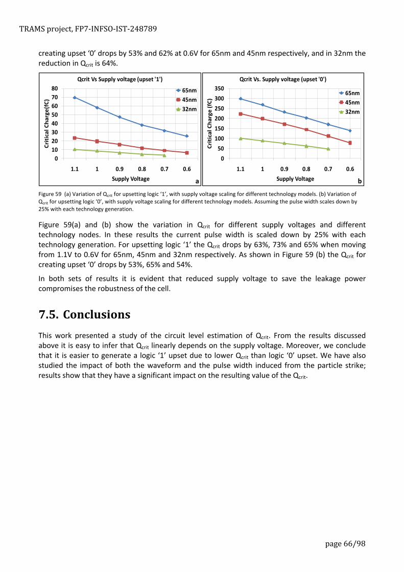
TRAMS project, FP7-‐INFSO-‐IST-‐248789
page 66/98
creating upset ‘0’ drops by 53% and 62% at 0.6V for 65nm and 45nm respectively, and in 32nm the reduction in Qcrit is 64%.
Figure 59 (a) Variation of Qcrit for upsetting logic ‘1’, with supply voltage scaling for different technology models. (b) Variation of Qcrit for upsetting logic ‘0’, with supply voltage scaling for different technology models. Assuming the pulse width scales down by 25% with each technology generation.
Figure 59(a) and (b) show the variation in Qcrit for different supply voltages and different technology nodes. In these results the current pulse width is scaled down by 25% with each technology generation. For upsetting logic ‘1’ the Qcrit drops by 63%, 73% and 65% when moving from 1.1V to 0.6V for 65nm, 45nm and 32nm respectively. As shown in Figure 59 (b) the Qcrit for creating upset ‘0’ drops by 53%, 65% and 54%.
In both sets of results it is evident that reduced supply voltage to save the leakage power compromises the robustness of the cell.
7.5. Conclusions This work presented a study of the circuit level estimation of Qcrit. From the results discussed above it is easy to infer that Qcrit linearly depends on the supply voltage. Moreover, we conclude that it is easier to generate a logic ‘1’ upset due to lower Qcrit than logic ‘0’ upset. We have also studied the impact of both the waveform and the pulse width induced from the particle strike; results show that they have a significant impact on the resulting value of the Qcrit.
01020304050607080
1.1 1 0.9 0.8 0.7 0.6
Critical C
harge(fC)
Supply Voltage
Qcrit Vs Supply voltage (upset '1')
65nm45nm32nm
050100150200250300350
1.1 1 0.9 0.8 0.7 0.6
Critical C
harge (fC)
Supply Voltage
Qcrit Vs. Supply voltage (upset '0')
65nm45nm32nm
b a
TRAMS project, FP7-‐INFSO-‐IST-‐248789
page 67/98
8. Carbon Nanotube technology: Modeling and analysis of basic SRAM cells with CNTFETs.
In silicon bulk CMOS technology the variability of the device parameters is a key drawback and it may be a limiting factor for further miniaturizing nodes. In this section, the variability in Carbon nanotube Field Effect Transistor (CNFET) is evaluated as well as its real capability to be a promising alternative to Si-‐CMOS technology.
In a first part the impact of carbon nanotube (CNT) diameter variations and the presence of metallic CNTs (main sources of variability) in the transistor are analysed (device level). Both, different diameters and metallic CNTs are due to the lack of chirality control during the CNT growth process.
In a second part, a comparison between Si-‐CMOS (32nm, 22nm and 16nm Predictive Technology Models, and 18nm and 13nm models developed by UoG in TRAMS WP1) and CNFET 6T SRAM cells is realized (circuit level). First, a performance analysis is presented. All 6T cells are compared in terms of write time, access time, area, power consumption and read stability. Then an analysis introducing random VTH variations for different scenarios and temperatures is presented.
8.1. Introduction Carbon Nanotubes (CNTs) have been attracting much attention in recent years due to its small dimension, unusual geometry and their extraordinary electronic properties [60].
A CNT is a graphene sheet rolled up to form a hollow cylinder ( Figure 60). A CNT can be semiconducting or metallic depending on the angle of the atom arrangement along the tube. This is referred as the chirality vector and is represented by the integer pair (n, m): Ch = na1 + ma2 = (n, m), where n and m (wrapping indices) are integers and a1 and a2 are the unit vectors of the graphene lattice. A simple method to determine whether a CNT is metallic or semiconducting is based on considering the indexes (n, m), i.e. the nanotube is metallic if n=m or n-‐m=3i, where i is an integer. The diameter of the CNT also depends on the chirality. It can be calculated as ! =!!!!! !! +!! + !", where acc is the nearest-‐neighbour carbon atom distance of 0.142 nm.
Transistors made of CNTs or Carbon Nanotube Field Effect Transistors (CNFETs) are promising candidates to replace silicon CMOS due to its high performance; mainly a high current driving capability, tolerance to temperature drift, leakage currents avoidance and self assembly growth [61]. A CNFET is essentially a conventional MOSFET, except that its channel is made up of one or more CNTs. In a MOSFET-‐like CNFET the CNTs present two un-‐gated heavily doped segments between the gate and the source/drain and an intrinsic gated region as is shown in Figure 61(left).
Stanford University has developed a compact SPICE model for MOSFET-‐like CNFET simulation [5] [62]. This model is implemented in three levels ( Figure 61,right). Level 1, CNFET-‐L1, models the intrinsic behaviour of CNFET. The second level, CNFET-‐L2, includes the device non-‐idealities. The first two levels deal with only one CN under the gate. The top level, CNFET-‐L3, models the interface between the CNFET device and CNFET circuits. This level deals with multiple CNs per device and includes the parasitic gate capacitance and screening due to adjacent CNTs. We have used this model for our HSPICE simulations.

TRAMS project, FP7-‐INFSO-‐IST-‐248789
page 68/98
Exceptional I-‐V characteristics have been demonstrated in ”ideal” CNFETs (meaning all CNTs are semiconducting, have the same diameter and are aligned and well-‐positioned) [63]. However, in reality, at least from the research results obtained up to now, there are some imperfections inherent to CNT synthesis and CNFET manufacturing process that may eclipse the expectations. So, as mentioned before, in this first section we analyse the main source of variability: the lack of chirality control during the CNT growth process. This limitation is responsible for the percentage of metallic CNTs and the random distribution of CNT diameters.
Figure 60. (Left) Schematic diagram of a graphene layer and how it can be rolled to form a carbon nanotube. (Right) Chiral vector in
the graphene layer.
Figure 61. (Left) MOSFET-‐like CNT transistor. Two different regions can be distinguished: intrinsic region and heavily doped S/D regions. (Right) Complete CNFET Stanford model
8.2. Sources of variation for CNFET Although CNFETs posses extraordinary properties that make them suitable for digital circuit applications, there are several limitations in CNT production methods and CNTFET manufacturing process that affect its performance and must be taken into account.
8.2.1. CNTs growth process limitations The most critical challenge in the CNTs growth process is to control the diameter and the proportion of metallic CNTs. In short, the control of chirality. With the main growth methods used

TRAMS project, FP7-‐INFSO-‐IST-‐248789
page 69/98
today, laser ablation, chemical vapour deposition (CVD), arc discharge and high-‐pressure CO decomposition (HPCO), a polydisperse mixture of CNTs with various chirality is obtained [64].
Metallic CNTs (m-‐CNTs) should not be used to make CNTFETs. They present a high conductivity that makes that its current cannot be controlled by the gate, causing source-‐drain shorts in the transistor. On the other hand, diameter variations, caused by the respective growth method affect the electrical properties of the transistors such as the drive current and the threshold voltage.
1. Percentage of m-‐CNTs: A typical synthesis process produces 1/3 of m-‐CNTs and 2/3 of semiconducting (s-‐CNTs). Although recent CNT growth techniques can achieve as high as 90% of s-‐CNTs [65] and even 96% [66] there is not technique available today to grow 100% s-‐ CNTs. Therefore, different m-‐CNTs removal techniques after growth, such as electrical burning and selective chemical etching are necessary.
2. Diameter variations: As in the previous case, there is not still a process that synthesizes nanotubes of only a unique diameter. Depending on the production method of CNTs, different mean diameters and diameter distributions can be observed [64].
8.2.2. CNFETs fabrication process limitations An ”ideal” MOSFET-‐like CNFET (Doped-‐S/D CNFET) is composed by one or more perfectly aligned carbon nanotubes whose section under the gate is intrinsic and the source/drain extension regions are n/p doped. There are also some challenges in the CNFET manufacturing process.
1. Doping variations: Controlled doping is very difficult and doping S/D variations cause drive current variations in CNFETs [67] [68].
2. Misaligned CNTs: Mispositioned and misaligned CNTs may cause shorts in CNFETs. Impressive achievements have been obtained in this field through the use of quartz substrate. More than 99% of the CNTs lie along the direction of the quartz [69]. Even for CNTs on quartz substrates, a non-‐negligible fraction of CNTs are misaligned. It is really difficult to position and align all the CNTs for all CNFETs properly.
In the next section we will focus on the CNT growth process limitations. We examine how the proportion of m-‐CNTs affects the CNFET performance (in terms of transistor parameter variability) for a given diameter distribution and a number (N) of nanotubes per transistor.
8.3. CNFET Model, CNT growth variations and simulation methodology
8.3.1. CNFET model The CNFET structure is shown in Figure 62. The main device parameters used in this work are summarized in Table 13, with the aim of defining a CNFET with a size between that of 16nm and 32nm silicon bulk transistors. As can be observed, we assume that each CNFET is composed by N CNTs (N-‐tubes CNFET). We consider a nominal value of N=8, following the selection of the number of CNTs exposed in [70] by reliability reasons. The inter-‐CNT spacing is 4 nm (parameter affecting the charge screening effect) and the length of the S/D extensions and the gate is 16 nm. The width of the metal gate is 36 nm for the nominal value of N.

TRAMS project, FP7-‐INFSO-‐IST-‐248789
page 70/98
Figure 62.CNFET device model [5] [62]
Fixed parameters
Power supply 0.9V
Oxide thickness 4nm
Gate/Source/Drain length (CNT) 16nm
Width of the metal gate 36nm
CNT pitch 4nm
Table 13.Device parameters and process assumptions.
8.3.2. CNT growth variations The chirality is a key factor in a CNFET, because is responsible of the CNT behaviour, diameter and the threshold voltage of the 1-‐tube transistor. It has to be noted that the threshold voltage of a CNFET can be calculated from the chirality as follows.
!!" =!!2! =
!!!!!!"#
where the parameter a (~2.49!) is the carbon to carbon atom distance, !! (~3.033 !") is the carbon π-‐π bond energy in the tight bonding model, e is electronic charge and DCNT is the CNT diameter.
As mentioned before, the mean diameters and the diameter distribution depend on the CNT growth method [64]. For example, using laser ablation process (in general) a Gaussian diameter distribution is observed with a diameters mean of 1.4 nm and a standard deviation (STD) of 0.3 nm, whereas with methods such as CVD and HPCO the CNT diameters are found to be spread over a wide range with a minimum diameter of 0.7 nm, and maximum diameter of 6 nm and a decaying probability for higher diameters [64]. This occurs because the diameter distribution depends on the density and the diameter of the catalytic nanoparticles as well as other factors such as growth conditions and growth temperature. We assume an asymmetrical Chi distribution of diameters with a range between 1nm and 6 nm (Table 13). The mean and the STD of this function are 2.9 nm and 0.7 nm respectively. This distribution covers 10 possible diameters of s-‐CNTs (see Figure 63). Then, we also consider a hypothetical manufacturing process with a narrower diameter distribution. In this case we use a Gaussian distribution of diameters with a range between 1nm and 2nm.
Variable parameters
Number of CNTS per device (N) Nominal:8 Range:4-‐12
CNT diameter (D) 1nm-‐6 nm Chi distribution
1nm-‐2nm Gaussian distribution
Metallic CNT proportion (TM) 0% -‐ 33%

TRAMS project, FP7-‐INFSO-‐IST-‐248789
page 71/98
We assume that all m-‐CNTs can be broken by a perfect removal process, not being m-‐CNTs actives in the N-‐tubes CNFET. In our analysis the probability of a CNT be metallic is between 0% (all CNTs are semiconducting) and 33% (typical synthesis process).
Due to both limitations, proportion of m-‐CNTs and diameter variations, it has to be noted that it is also important to determine the number of CNTs per transistor (N) in order to guarantee a good CNFET performance. In [70], a number of tubes N=8 is proposed. In our work, we consider this number but we also analyze a range of N between 4 and 12.
8.3.3. The simulation methodology Figure 63 shows the simulating procedure used to evaluate the distributions of the threshold voltage (VTH) and the equivalent transconductance factor (K) in a scenario of growing variability as the discussed above. The factors in the analysis are:
• The number of CNTs used in the CNFET implementation, N.
• The proportion of m-‐CNTs in the growing process, TM.
• The diameter distribution of semiconductor CNTs, D, a random variable.
Given a set of N, TM and D distribution, the analysis process is displayed in a simplified way in Figure 63. A sample of CNFET is obtained getting N nanotubes in an ordered extraction. Some of them are m-‐CNTs (M), randomly selected following the proportion TM, and the rest are s-‐CNTs (S). M-‐CNTs are assumed to be perfectly broken by a burn removal technique, whereas a diameter is assigned to each s-‐ CNTs extracted from the respective diameter distribution. So, the result is a sample of N-‐tubes CNFET, with M no active m-‐CNTs and S active s-‐CNTs.
For each CNFET sample the I-‐V characteristic is obtained. This is done through the summation of the N IDS current components (each CNT that forms the CNFET). The m-‐CNTs do not contribute (IDS = 0). S-‐CNTs are evaluated using the HSPICE CNFET model developed by Stanford University [5] [62] taking into account its diameter, the charge screening effects and the position of the CNT in the transistor (edge or middle).
Finally, we perform a 1000 samples Monte Carlo analysis obtaining an IDS − VDS characteristic distribution (see Figure 64). We also obtain the equivalent VTH and K from each sample and calculate the mean and the standard deviation, STD. It has to be noted that the VTH of each CNFET sample is the minimum VTH of the single-‐tube components of the transistor. The K is evaluated from the VDD saturated current level using the expression of the Sah [71] model for a equivalent Si-‐MOS transistor neglecting channel modulation and carriers saturation effects (as correspond to a CNFET).

TRAMS project, FP7-‐INFSO-‐IST-‐248789
page 72/98
Figure 63. Monte Carlo experiment and simulation methodology used.
Figure 64.Example of IDS-‐VDS distribution for 50 CNFET samples.
MONTE CARLO EXPERIMENT
CNFET sample extractionN CNTs
M metallic S semiconducting
diameterdistribution
D1
D2
D8
D5
D10
D1 D2 D3 D4 D5 D6 D7 D8 D9 D10D8
m-CNTbreakdown
(N-M)activesCNTs
CNFET with N tubes
Sample simulation
Stanford uniform CNFET model used for IDS characteristic generation for each CNT component (middle and edge cases)
10 diameters
Summation of the N components
D10edge D8edge
D2middle
I
V
X samples
IDS current distribution (X samples)
Obtention of equivalent K and VTH for each sample
Calculation of mean and STD of K and VTH variables
I
V
Results
1 2 3 ... N

TRAMS project, FP7-‐INFSO-‐IST-‐248789
page 73/98
8.4. Results of CNFET variation analysis The following figures show the mean and standard deviation for the VTH and the equivalent transconductance factor K obtained using the procedure previously presented. Both parameters characterize the device variability in CMOS technology; the first as threshold voltage and the second as a factor that includes the impact of the geometric parameters of the layout (transistor channel width and length).
Figure 65 and Figure 66 show the mean of VTH and K respectively. Mean of VTH of the CNFET increases with the probability of metallic tubes in the manufacturing process and decreases as the number of tubes per transistor grows. Figure 66 shows the effect on the mean of K, increasing with the number of tubes, as expected, but decreasing with the metallic probability. All these considerations are useful in the design phase but now we concentrate our attention on the parameters variability that is a key drawback for modern CMOS technologies.
Figure 65. Simulation results. Mean of VTH.
Figure 66. Simulation results. Mean of K.

TRAMS project, FP7-‐INFSO-‐IST-‐248789
page 74/98
Figure 67 and Figure 68 show the impact of N and TM on the STD of VTH and equivalent K. In Table 14 the percentages of variation (for 3 sigma) of VTH and K for N and TM corners are shown, including the results for the nominal value of N=8. For the threshold voltage, the maximum and the minimum percentage of variation are 67 % and 35 % that correspond to the corners (N = 4,TM = 33%) and (N = 12,TM = 0%) respectively. These values imply that even for current CNFET manufacturing capabilities, the variation in the threshold voltage is much lower than the expected for 32 and 16 Si-‐CMOS technologies. Because the ITRS [23] predicts that they may reach 70% and 100% of percentage variation. In the case of K, observe that the higher is the number of tubes (N) the lower the variability for both TM probabilities. Consequently there is a trade-‐off between device size and variability (caused by N) that designers should take into account.
Figure 67. STD of VTH.
Figure 68. STD of K.

TRAMS project, FP7-‐INFSO-‐IST-‐248789
page 75/98
For an ideal case of no m-‐CNTs in the manufacturing process (TM = 0%), we obtain a percentage of variation for VTH and K that goes from 35% to 48% and from 35% to 69% respectively, that is much lower than the expected for 32nm and 16nm conventional technologies. So, the reduction of the metallic proportion is a key factor for the development of CNFET circuits.
Parameter VTH K
Number of tubes N=4 N=8 N=12 N=4 N=8 N=12
TM=0% 48% 39% 35% 69% 46% 35%
TM=33% 67% 46% 39% 130% 98% 79%
Table 14.VTH and K variation for 1000 samples and a Chi distribution of diameters.
For this last case (TM = 0%) the only reason of variability is the diameter distribution of the CNTs. If we consider a hypothetical manufacturing process with a narrower distribution (Gaussian diameter distribution with a mean and STD of 1.5 nm and 0.16 nm respectively) the percentage of variation would be between 16% (N=12) and 23% (N=4) for VTH and between 17% and 25% for K (see Table 15). This would allow a design scenario where variability would not be a critical factor as it is nowadays in conventional CMOS.
Parameter VTH K
Number of tubes N=4 N=8 N=12 N=4 N=8 N=12
TM=0% 23% 21% 16% 25% 20% 17%
TM=33% 42% 24% 22% 116% 87% 66%
Table 15. VTH and K variation for 1000 samples and a Gaussian distribution of diameters.
So, considering a range of metallic tubes from 33% (current growth methods) to 0% (perfection) and a realistic distribution of diameters, it has been shown that the variability of both K factor and VTH is lower than CMOS for transistors with just 8 nanotubes, and much better for 12 tubes. Even for the case of only 4 tubes per transistor the observed variability is similar to the expected for CMOS. In a future scenario with a narrower distribution of diameters, variation for both parameters could reach levels from 16% to 25%, fact that would allow a design procedure without the stress caused by variability in current conventional technology.

TRAMS project, FP7-‐INFSO-‐IST-‐248789
page 76/98
8.5. Variability analysis and performance in CMOS and CNFET SRAM 6T cells
In order to evaluate the potential of CNFETs as possible alternative to Si-‐MOSFETs technology at circuit level, a comparison between Si-‐CMOS and CNFET 6T SRAM cells has been realized. First, we compare them in terms of Write time, Access time, area, power consumption and read stability (nominal comparison). Then, we investigate the effects of VTH and temperature on the characteristics of the different SRAM cells (variability comparison).
8.5.1. Model and parameters definition for 6T cell A typical 6T SRAM cell is shown in Figure 69. This cell has been implemented using different technologies: 16nm, 22nm, 32nm, and 18nm, 13nm CMOS technologies and CNFET technology. The width (W, in nm) and length (L, in nm) ratio of each transistor for CMOS technologies are also shown in Figure 69 (in red), where T is the Technology parameter and depends on the technology size. It takes the values shown in Table 16. For CNFET technology, all transistors have the same size, W=32nm (8 tubes) and L=16nm. HSPICE simulations are performed using Berkeley high-‐performance Predictive Technology Models (PTM) [4], 13nm and 18nm CMOS models developed by the UoG (TRAMS WP1), and carbon nanotube technology model [5] [62]. These models and the supply voltage for each one are shown in Table 16.
Figure 69. Schematic of a typical 6T SRAM cell.
Table 16.Models, technologies and supply voltage.
Model PTM TRAMS WP1 CNFET
Technology size 32nm 22nm 16nm 18nm 13nm 8 tubes
T 16nm 11nm 8nm 9nm 6.5nm W=32nm,L=16nm
VDD 1V 1V 1V 0.7V 0.7V 1V
TRAMS project, FP7-‐INFSO-‐IST-‐248789
page 77/98
The value of bitline capacitances depends on the technology. The bitline capacitances (CBL, CBLB) have been calculated as the sum of the junction capacitance of the access transistors (Cj) of each cell plus the wire capacitance (Cwire). We consider 256 cells.
CBL =Cj !cells+Cwire =Cjc +Cwire For CMOS technology we assume that the wire capacitance is approximately 5 times Cjc. So, the final expression for the CBL (CBLB) is
CBL =Cjc +Cwire =Cjc + 5Cjc = 6Cjc
For CNFETs the junction capacitance is negligible so we just take into account the wire capacitance that is similar to 16nm.
The value of the bitline capacitances for each technology is shown in Table 17.
Table 17. Bitline capacitance values for each technology.
8.5.2. CNFET SRAM cell versus Si-‐MOSFET SRAM cell (nominal comparison)
8.5.2.1 Write time and Access time Write time and Access time are two important metrics for assessing the performance of a SRAM cell. In this document, the Write time is defined as the time required for changing the cell contents (store node reaches 0.6VDD for write ‘1’ or 0.4 VDD for write ‘0’) after the wordline is turned on (Voltage(WL)=0.5VDD). The Access time is defined as the time required for producing a prespecified voltage difference (0.1V) between BL and BLB after the wordline is turned on. This voltage difference is sensed by sense amplifier.
The results for both times are shown in Figure 70.
As can be observed both times decrease as the technology size decreases for PTM and TRAMS WP1 CMOS technologies. CNFET technology shows the least Write time (7.77ps) and Access time (57.42ps).
PTM TRAMS WP1 CNFET Capacitance 32nm
(W=64nm) 22nm
(W=44nm) 16nm
(W=32nm) 18nm
(W=36nm) 13nm
(W=26nm) 8 tubes
Cj (aF) 38.48 25.09 17.35 15.71 10.30 negligible Cjc (fF) 9.85 6.42 4.44 4.02 2.64 negligible
Cwire (fF) 49.26 32.12 22.21 20.11 13.21 22.21 (similar to 16nm) CBL (fF) 59.11 38.54 26.65 24.13 15.85 22.21
TRAMS project, FP7-‐INFSO-‐IST-‐248789
page 78/98
Figure 70. Write time and Access time for each technology.
8.5.2.2 Area, Power Consumption and Read Stability
The area of the 6T cell for each node technology has been calculated basing on [16], obtaining the following size (
Table 18). Obviously the area decreases as the technology size decreases. The area of CNFET is similar to 16nm area.
Static power consumption is very low for CNFET. This is because the CNFET has a significantly higher ON-‐OFF current ratio compared to the MOSFET in deep-‐submicron range. Dynamic power consumption is also less in CNFET than in PTM Si-‐MOSFET models but it is higher than in TRAMS WP1 models.
Read stability is measured by the Static Noise Margin (SNM), that is defined as the maximum value of DC noise voltage that can be tolerated by the SRAM cell without changing the stored bit. So, as
higher is the SNM more robust is the cell. As is shown in
Table 18 the most stable cell is the CNFET.
!!"!#$ %&"''$ %(")*$!*"'!$ !+"&)$
)"))$
%+,$
#)"+%$
)*"%,$
%*&"#$
&,")($
,)"'!$
!"
#!"
$!"
%!"
&!"
'!!"
'#!"
'$!"
'%!"
(#)*" ##)*" '%)*" '&)*" '()*" +,-./"
01234"5*4"6789"
:;;488"5*4"6789"
PTM TRAMS WP1 CNFET 32nm 22nm 16nm 18nm 13nm 8 tubes
Cell area (µm2) 0.29 0.14 0.07 0.09 0.045 0.09 Static Power (pW) 109.60 112.40 279.60 428.10 379.20 5.82
Dynamic power (µW) 7.17 4.91 3.94 1.53 1.26 3.06
TRAMS project, FP7-‐INFSO-‐IST-‐248789
page 79/98
Table 18. 6T cell performance for each technology.
8.5.3. CNFET SRAM cell versus Si-‐MOSFET SRAM cell (variability comparison) In this section we consider random VTH variations in 6T SRAM cells. For CMOS technologies we take into account the scenarios shown in
Table 19 (moderated, high and very high). In column 3 the percentage of VT H variation (100 × σ/μ) for minimum transistor size is shown; in order to adapt it to our transistor size, we have corrected these values with !"#$"%&'("/ !". Final values of VTH variability used in this document are shown in column 4. For CNFET we consider 15.58% of VTH variation (Table 20). This value has been obtained from the mean (0.12V) and the STD (18.7mV) of VTH extracted following the method presented in section 6.3.3 for 8 tubes and 33% of m-‐CNTs probability. We have also analysed the impact of these variations for three different temperatures: 25 ◦C, 60 ◦C and 100 ◦C
Si-‐Bulk Technology
Scenario Random(min.size) 100 x 1 σ/average
Random (corrected) !"#$"%&'("/ !"
VTH VTH 32nm moderated 6% 4.24%
high 15% 10.61% 22nm moderated 8% 5.66%
high 15% 10.61% very high 30% 21.21%
16nm moderated 10% 7.07% high 20% 14.14%
very high 40% 28.28% 18nm very high 58% 41.01% 13nm very high 58% 41.01%
Table 19. Scenarios considered for each technology.
CNFET Technology
NCNFET VTH
PCNFET VTH
Random 6T cell 100 x 1 σ/average
µ (V) σ (V) µ (V) σ (V) VTH 0.12 0.0187 -‐0.12 0.0187 15.58%
Table 20.VTH variability for CNFET technology.
The mean (µ) and the STD (σ) of the Write time and Access time have been measured for each scenario and each temperature. These values have been obtained for 500 samples. Also, the variability for 3σ and the percentage of errors are shown in the next tables. Noted that the percentage of errors include flipping errors and errors due to an excessive time. The percentage of flipping errors is shown in brackets.
Read SNM (mV) 296 262.90 218 202.80 195.50 302.50

TRAMS project, FP7-‐INFSO-‐IST-‐248789
page 80/98
8.5.3.1 Write time 32nm PTM
Random 6T cell 100 x 1σ /average
25ºC
60ºC
100ºC
VTH variation µ (ps) STD (ps) µ (ps) STD (ps) µ (ps) STD (ps) 4.24% (6%) 22.36 0.82 26.66 1.24 33.13 1.72
10.61% (15%) 22.77 2.33 27.69 4.39 35.13 6.47 25ºC
errors (%) 60ºC
errors (%) 100ºC
errors (%) 4.24% (6%) 0 0 0
10.61% (15%) 0 0.20 (0) 1 (0) 25ºC
100x3σ /µ (%) 60ºC
100x3σ /µ (%) 100ºC
100x3σ /µ (%) 4.24% (6%) 11.03 13.96 15.53
10.61% (15%) 30.72 47.63 55.27
Table 21.Write time variation for 32nm PTM.
22nm PTM Random 6T cell
100 x 1σ /average 25ºC
60ºC
100ºC
VTH variation µ (ps) STD (ps) µ (ps) STD (ps) µ (ps) STD (ps) 5.66% (8%) 19.37 1.03 23.58 1.48 29.49 2.12
10.61% (15%) 19.66 1.99 24.23 2.99 30.81 5.33 21.21% (30%) 21.82 6.82 28.22 11.65 34.73 12.43
25ºC errors (%)
60ºC errors (%)
100ºC errors (%)
5.66% (8%) 0 0 0 10.61% (15%) 0.4 (0) 1.2 (0) 3.2 (0) 21.21% (30%) 11 (0.2) 17 (0.2) 23.4 (0.4)
25ºC 100x3σ /µ (%)
60ºC 100x3σ /µ (%)
100ºC 100x3σ /µ (%)
5.66% (8%) 15.89 18.81 21.57 10.61% (15%) 30.50 37.07 52.06 21.21% (30%) 93.72 123.87 107.38
Table 22.Write time variation for 22nm PTM.
16nm PTM Random 6T cell 1 100 x 1σ /average
25ºC 60ºC 100ºC
VTH variation µ (ps) STD (ps) µ (ps) STD (ps) µ (ps) STD (ps) 7.07% (10%) 16.99 1.11 20.94 1.59 26.08 2.32
14.14% (20%) 17.57 2.38 22.13 4.33 28.05 6.61

TRAMS project, FP7-‐INFSO-‐IST-‐248789
page 81/98
28.28% (40%) 21.65 11.94 25.99 11.49 33.73 15.48 25ºC
errors (%) 60ºC
errors (%) 100ºC
errors (%) 7.07% (10%) 1.2 (0) 5.6 (0) 12.2 (0)
14.14% (20%) 11.6 (0) 20.2 (0) 26.6 (0.2) 28.28% (40%) 30.4 (2) 40 (3.4) 47 (4.6)
25ºC 100x3σ /µ (%)
60ºC 100x3σ /µ (%)
100ºC 100x3σ /µ (%)
7.07% (10%) 19.65 22.72 26.69 14.14% (20%) 40.63 58.65 70.68 28.28% (40%) 165.39 132.69 137.68
Table 23.Write time variation for 16nm PTM.
18nm WP1 TRAMS Random 6T cell
1 100 x 1σ /average 25ºC 60ºC 100ºC
VTH variation µ (ps) STD (ps) µ (ps) STD (ps) µ (ps) STD (ps) 41.01% (58%) 27.86 13.89 28.25 13.14 28.59 12.32
25ºC errors (%)
60ºC errors (%)
100ºC errors (%)
41.01% (58%) 10.8 (1.6) 10.2 (1.4) 11.2 (1.8) 25ºC
100x3σ /µ (%) 60ºC
100x3σ /µ (%) 100ºC
100x3σ /µ (%) 41.01% (58%) 149.59 139.57 129.29
Table 24.Write time variation for 18nm WP1 TRAMS.
13nm WP1 TRAMS Random 6T cell
100 x1σ /average 25ºC 60ºC 100ºC
VTH variation µ (ps) STD (ps) µ (ps) STD (ps) µ (ps) STD (ps) 41.012%(58%) 27.86 16.68 27.75 16.19 28.72 16.36
25ºC errors (%)
60ºC errors (%)
100ºC errors (%)
41.012%(58%) 33.4 (5.8) 34.6 (6) 39.2 (7.2) 25ºC
100x3σ /µ (%) 60ºC
100x3σ /µ (%) 100ºC
100x3σ /µ (%) 41.012%(58%) 179.59 175.11 170.86
Table 25.Write time variation for 13nm WP1 TRAMS.
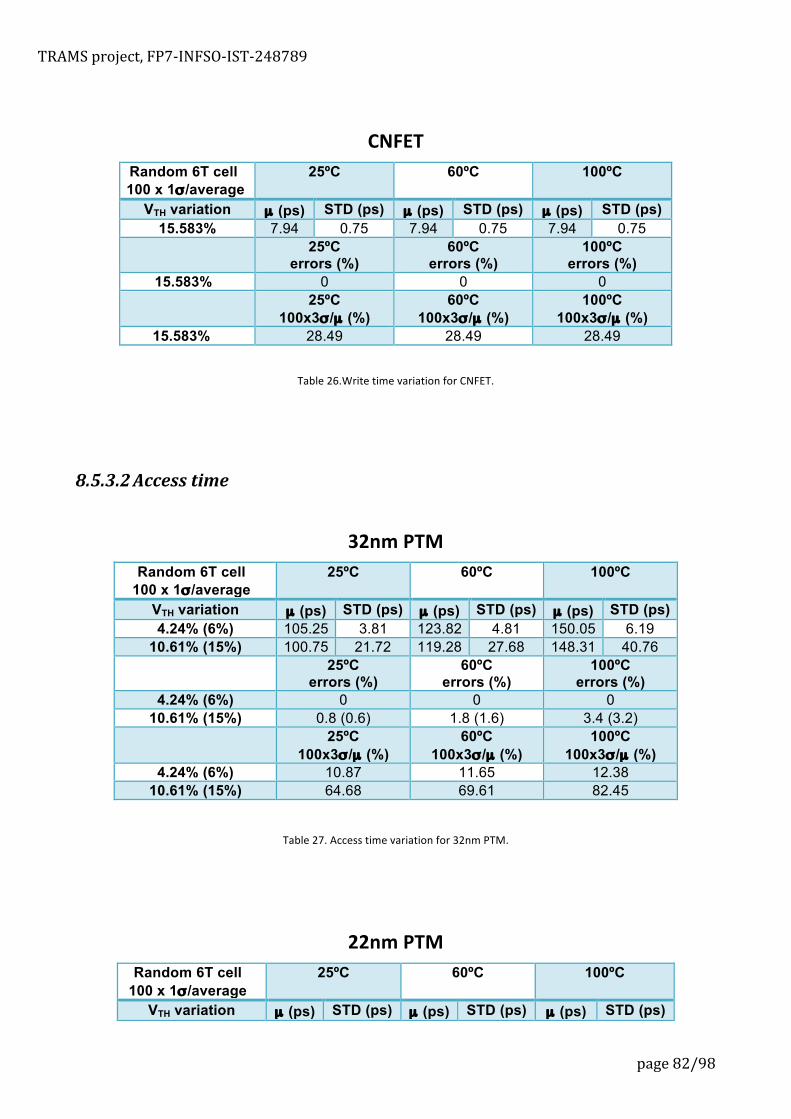
TRAMS project, FP7-‐INFSO-‐IST-‐248789
page 82/98
CNFET Random 6T cell
1 100 x 1σ /average 25ºC 60ºC 100ºC
VTH variation µ (ps) STD (ps) µ (ps) STD (ps) µ (ps) STD (ps) 15.583% 7.94 0.75 7.94 0.75 7.94 0.75
25ºC errors (%)
60ºC errors (%)
100ºC errors (%)
15.583% 0 0 0 25ºC
100x3σ /µ (%) 60ºC
100x3σ /µ (%) 100ºC
100x3σ /µ (%) 15.583% 28.49 28.49 28.49
Table 26.Write time variation for CNFET.
8.5.3.2 Access time
32nm PTM Random 6T cell
100 x 1σ /average 25ºC
60ºC
100ºC
VTH variation µ (ps) STD (ps) µ (ps) STD (ps) µ (ps) STD (ps) 4.24% (6%) 105.25 3.81 123.82 4.81 150.05 6.19
10.61% (15%) 100.75 21.72 119.28 27.68 148.31 40.76 25ºC
errors (%) 60ºC
errors (%) 100ºC
errors (%) 4.24% (6%) 0 0 0
10.61% (15%) 0.8 (0.6) 1.8 (1.6) 3.4 (3.2) 25ºC
100x3σ /µ (%) 60ºC
100x3σ /µ (%) 100ºC
100x3σ /µ (%) 4.24% (6%) 10.87 11.65 12.38
10.61% (15%) 64.68 69.61 82.45
Table 27. Access time variation for 32nm PTM.
22nm PTM Random 6T cell
100 x 1σ /average 25ºC
60ºC
100ºC
VTH variation µ (ps) STD (ps) µ (ps) STD (ps) µ (ps) STD (ps)

TRAMS project, FP7-‐INFSO-‐IST-‐248789
page 83/98
5.66% (8%) 77.65 19.53 89.18 24.89 105.97 31.96 10.61% (15%) 78.45 20.53 91.44 26.59 109.71 37.76 21.21% (30%) 79.10 39.70 92.05 52.46 108.07 51.95
25ºC errors (%)
60ºC errors (%)
100ºC errors (%)
5.66% (8%) 0.2 (0) 0.2 (0) 0.2 (0.2) 10.61% (15%) 2.8 (1.2) 4.4 (3.2) 7.6 (5.2) 21.21% (30%) 19.4 (11.4) 24.8 (15.8) 31.8 (19.6)
25ºC 100x3σ /µ (%)
60ºC 100x3σ /µ (%)
100ºC 100x3σ /µ (%)
5.66% (8%) 75.45 83.74 90.46 10.61% (15%) 78.49 87.24 103.25 21.21% (30%) 150.58 170.96 144.22
Table 28. Access time variation for 22nm PTM.
16nm PTM Random 6T cell
1 100 x 1σ /average 25ºC 60ºC 100ºC
VTH variation µ (ps) STD (ps) µ (ps) STD (ps) µ (ps) STD (ps) 7.07% (10%) 73.25 6.089 92.29 20.71 118.34 34.51
14.14% (20%) 72.28 26.17 87.95 29.63 110.44 46.84 28.28% (40%) 71.33 38.89 89.48 60.44 109.36 62.35
25ºC errors (%)
60ºC errors (%)
100ºC errors (%)
7.07% (10%) 1.8 (1.8) 5.6 (5.6) 14.2 (13.6) 14.14% (20%) 14.2 (13) 22.4 (20.6) 29 (25.6) 28.28% (40%) 34.6 (25.8) 42.4 (30.8) 46.2 (33)
25ºC 100x3σ /µ (%)
60ºC 100x3σ /µ (%)
100ºC 100x3σ /µ (%)
7.07% (10%) 24.94 67.32 87.48 14.14% (20%) 108.62 101.06 127.24 28.28% (40%) 163.56 202.64 171.04
Table 29. Access time variation for 16nm PTM.
18nm WP1 TRAMS Random 6T cell
1 100 x 1σ /average 25ºC 60ºC 100ºC
VTH variation µ (ps) STD (ps) µ (ps) STD (ps) µ (ps) STD (ps) 41.01% (58%) 153.23 55.37 166.96 63.01 177.71 60.07
25ºC errors (%)
60ºC errors (%)
100ºC errors (%)
41.01% (58%) 14 (11.4) 18.4 (16.6) 23.8 (20.8)

TRAMS project, FP7-‐INFSO-‐IST-‐248789
page 84/98
25ºC 100x3σ /µ (%)
60ºC 100x3σ /µ (%)
100ºC 100x3σ /µ (%)
41.01% (58%) 108.39 113.23 101.40
Table 30. Access time variation for 18nm WP1 TRAMS.
13nm WP1 TRAMS Random 6T cell
100 x 1σ /average 25ºC 60ºC 100ºC
VTH variation µ (ps) STD (ps) µ (ps) STD (ps) µ (ps) STD (ps) 41.01% (58%) 107.17 65.75 111.45 65.63 122.67 70.98
25ºC errors (%)
60ºC errors (%)
100ºC errors (%)
41.01% (58%) 31 (20.4) 33.6 (23.6) 37.4 (29.6) 25ºC
100x3σ /µ (%) 60ºC
100x3σ /µ (%) 100ºC
100x3σ /µ (%) 41.01% (58%) 184.04 176.65 173.58
Table 31. Access time variation for 13nm WP1 TRAMS.
CNFET Random 6T cell
1 100 x 1σ /average 25ºC 60ºC 100ºC
VTH variation µ (ps) STD (ps) µ (ps) STD (ps) µ (ps) STD (ps) 15.58% 54.95 1.89 54.95 1.89 54.95 1.89
25ºC errors (%)
60ºC errors (%)
100ºC errors (%)
15.58% 0 0 0 25ºC
100x3σ /µ (%) 60ºC
100x3σ /µ (%) 100ºC
100x3σ /µ (%) 15.58% 10.33 10.33 10.33
Table 32. Access time variation for CNFET.
8.5.4. Results and discussion In general in Si-‐CMOS technologies, for both read and write times the variability (100x3σ/µ) increases as the scenario gets worse variability and as the temperature increases. In CNFETs they practically remain constant with the temperature because temperature has a low effect in CNFET technology as can be observed in Figure 71. The oscillation frequency (for a 11 stages oscillator) decreases as temperature increases for a 16nm PTM technology whereas it remains constant for CNFET technology.
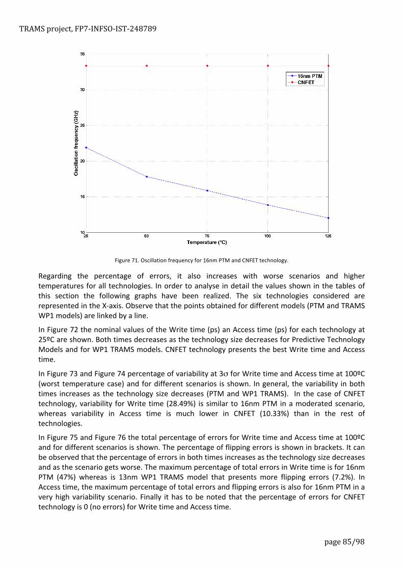
TRAMS project, FP7-‐INFSO-‐IST-‐248789
page 85/98
Figure 71. Oscillation frequency for 16nm PTM and CNFET technology.
Regarding the percentage of errors, it also increases with worse scenarios and higher temperatures for all technologies. In order to analyse in detail the values shown in the tables of this section the following graphs have been realized. The six technologies considered are represented in the X-‐axis. Observe that the points obtained for different models (PTM and TRAMS WP1 models) are linked by a line.
In Figure 72 the nominal values of the Write time (ps) an Access time (ps) for each technology at 25ºC are shown. Both times decreases as the technology size decreases for Predictive Technology Models and for WP1 TRAMS models. CNFET technology presents the best Write time and Access time.
In Figure 73 and Figure 74 percentage of variability at 3σ for Write time and Access time at 100ºC (worst temperature case) and for different scenarios is shown. In general, the variability in both times increases as the technology size decreases (PTM and WP1 TRAMS). In the case of CNFET technology, variability for Write time (28.49%) is similar to 16nm PTM in a moderated scenario, whereas variability in Access time is much lower in CNFET (10.33%) than in the rest of technologies.
In Figure 75 and Figure 76 the total percentage of errors for Write time and Access time at 100ºC and for different scenarios is shown. The percentage of flipping errors is shown in brackets. It can be observed that the percentage of errors in both times increases as the technology size decreases and as the scenario gets worse. The maximum percentage of total errors in Write time is for 16nm PTM (47%) whereas is 13nm WP1 TRAMS model that presents more flipping errors (7.2%). In Access time, the maximum percentage of total errors and flipping errors is also for 16nm PTM in a very high variability scenario. Finally it has to be noted that the percentage of errors for CNFET technology is 0 (no errors) for Write time and Access time.
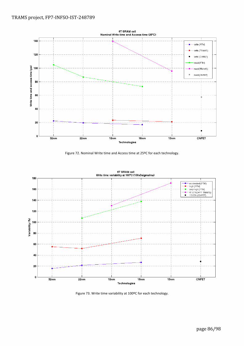
TRAMS project, FP7-‐INFSO-‐IST-‐248789
page 86/98
Figure 72. Nominal Write time and Access time at 25ºC for each technology.
Figure 73. Write time variability at 100ºC for each technology.
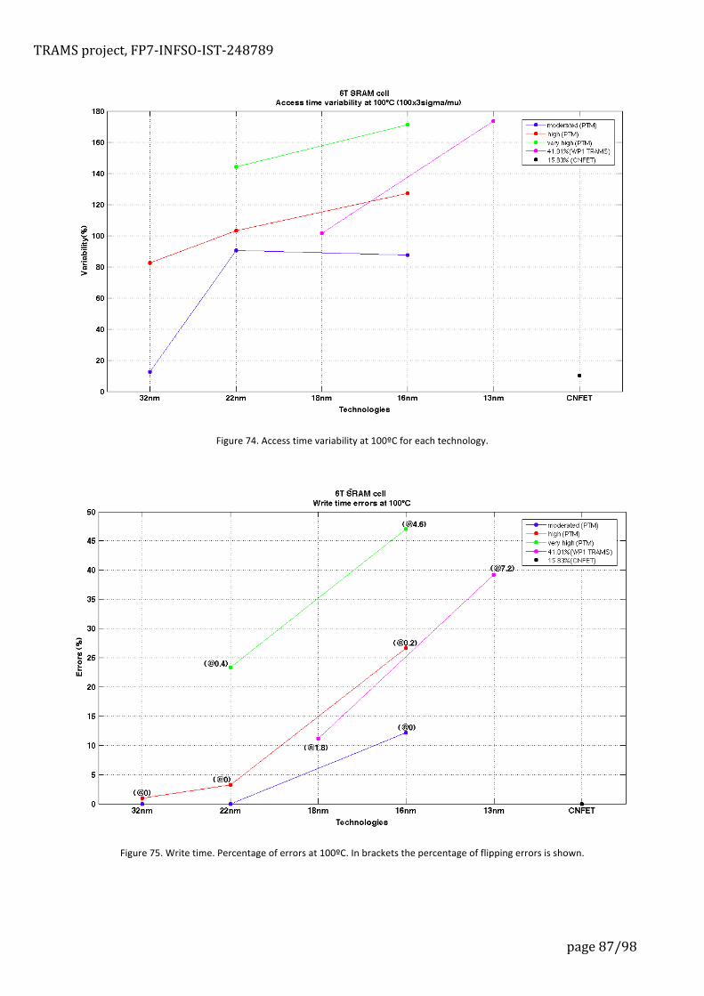
TRAMS project, FP7-‐INFSO-‐IST-‐248789
page 87/98
Figure 74. Access time variability at 100ºC for each technology.
Figure 75. Write time. Percentage of errors at 100ºC. In brackets the percentage of flipping errors is shown.

TRAMS project, FP7-‐INFSO-‐IST-‐248789
page 88/98
Figure 76. Access time. Percentage of errors at 100ºC. In brackets the percentage of flipping errors is shown.
8.6. Conclusions Carbon nanotubes FET (CNFET) technology exhibits a set of attractive characteristics in order to be considered as a potential alternative to CMOS in memory systems. Its low leakage current reduces the static consumption and it would be a key factor in dynamic memories. It sensitivity to temperature is practically null, this is an interesting factor compared with the very high sensitivity bulk technology present. Additionally is faster, not substantially faster if we compare with the high performance 18 and 13 nm technologies. However the implementation maturity of such a technology sill requires several years of development. It as a technology compatible with bulk CMOS but it will introduce complementary and expensive new processing steps. The variability analysis shows, as a promising perspective, that even for todays performance of growing carbon nanotubes the variability is comparable with the scenario of bulk technology considered in this work as moderate. With the improvements on the chirality control the potential variability would reach levels of a very controlled technology with variability lower than moderate.
TRAMS project, FP7-‐INFSO-‐IST-‐248789
page 89/98
9. General conclusions In this document the effects of environmental and process parameters fluctuations on the performance variability of memory cells and systems have been investigated. The work has concentrated mainly on bulk-‐CMOS technologies (key objective of the milestone MS2, M12) and, in order to compare them with a potential future alternative technology the work has been extended to CNFET technology.
The bulk-‐CMOS technologies can be divided into two groups, one is the set of open source technologies known as Predictive Technology Models (PTM), facilitated publically by the University of Arizona, covering 45, 32, 22 and 16 nm technology nodes. The second group of special interest are the bulk-‐CMOS 18 and 13 nm technologies developed by TRAMS in WP1 (Deliverable D1.1) on both variability and reliability aspects. For this last group we have considered in our analysis the nominal and variability models offered in WP1. In the case of the first group (PTM) we have used the nominal models provided by the University of Arizona and we have assumed three levels, or scenarios, of variability: moderate, high and very high. After the accurate results given from WP1 for 18 and 13 nm, we conclude that the most probable variability scenarios for PTM technologies are the corresponding to the high and manly very high levels. Regarding CNFET we have considered transistors composed by multiple nanotubes, between 4 and 12, with mean value 8 that is the number of nanotubes providing a good reliability level for such technology as showed the works of the University of Stanford.
The analysis at circuit level, performed from accurate electrical models using the previous device models and Hspice simulations, has been applied at two different levels: at specific bit-‐cell levels, that gives us the essential characteristics of each memorising technique, and at system level, understanding a complete 32KB cache memory system design. At bit-‐cell levels we have selected, in order to get complete and representative results, the 6Tcells for SRAM and the 1T1C and 3T1D cells for DRAM. The analysis at system (cache) level has been performed for both 6T and 3T1D type of cells. The environmental fluctuations considered are the silicon surface temperature and the local VDD voltage supply. Specific analysis about the impact of Single Event Upsets impact analysis has been developed for the 6T SRAM memories and an analysis about the aging effects caused by BTI has been also performed for 3T1D DRAM.
Among the main conclusions, we find that the main environmental factor is temperature, for all the type of circuits and technologies not using CNFETs (in fact the deeper node technology the more aggressive the effect). For sub-‐22nm technologies a typical factor is a decrease of 60% of the speed (read, write, access) of the memories, both bit-‐cell or system level, for an increase of temperature between room temperature and 110 oC. In the case of the dynamic memories the effects of the temperature on the retention time is dramatic with impressive reductions (1/100) for the same temperature increase. Also VDD fluctuations affect in the same way all type of memories, around a 15% of speed (the speed decreases when the voltage decreases) for 10% of voltage fluctuation.
The robustness of the 6T bit-‐cell for process variations (only random independent variations) has been performed using the concept of Satisfiability Boundary. The results show a dramatic drop of

TRAMS project, FP7-‐INFSO-‐IST-‐248789
page 90/98
yield for the variability levels determined in WP1 for 18 and 13 nm, as well as for the PTM technologies considering high and very high variability scenarios. Even for only 32KB the calculated yield is unacceptable and even null. The same results have been obtained for the case of 3T1D, perhaps more robust in comparison with 6T but also unacceptable or null yield. In the case of 1T1C results are even more dramatic. The reason for this is that in fact in the analysis of the 1T1C at bit (32 bit) cell level we have contemplated the modern circuit proposed by IBM for the eDRAM, where a sophisticated complementary circuit (to the basic 1T1C cell) is included in order to allow an automatic data recovery in read cycles. In general similar results have been obtained in the analysis of the 32KB memories for both 6T and 3T1D. For that case a percentage between 2 to 3% of the independent write-‐read cycles causes a data retention failure. These faults are on top of unacceptable decreases of speed (with sigmas of 34% of the nominal value).
About the analysis of reliability drop caused by BTI aging it has been shown that for both 3T1D (analysis performed in this deliverable) and 6T (obtained from publications from other researchers) degradation is a key limiting factor, causing dramatic yield drops if no countermeasure is implemented.
In the analysis of the 32nm technology in front of SEU (SRAM) it has been shown that the critical charge required to cause flips drops from 60 to 15 (fC) when we consider 65 and 32 nm technologies, and the effect is even more drastic when we reduce VDD levels in stand-‐by operations. This reduction of the critical charge is expected to follow the same dramatic trend for sub-‐22nm technologies.
Figure 77. Overall impact of variations on performances and reliability for sub-‐18nm technologies
In Section 8 a complete comparison analysis at bit-‐cell level for bulk-‐CMOS and CNFET technologies has been developed, only for the 6T cell. Results are interesting and could imply a

TRAMS project, FP7-‐INFSO-‐IST-‐248789
page 91/98
hope for the future of memories implemented in emerging technologies (CNTFETS and presumably others). With similar speed and cell area than the corresponding to bulk-‐16nm, SRAM cells implemented with CNTFETS exhibit very interesting results: practically an independence of temperature fluctuations (similar VDD sensitivity), much higher SNM, much lower static consumption (1/100 less of leakage current) with similar dynamic consumption and finally a much higher robustness (and consequently theoretical yield) in front of process variations, conditioned to the future development of the technology. Even for the poor capability to grow nanotubes we have today the scenario of variability is between moderate and high, but if we accept assumable improvements on the control of chirality we obtained variations effects better than moderate.
Figure 77 shows as a matter of general picture, the speed performance variability levels for the different fluctuating causes. Temperature and random process variability are the two key impacting mechanisms. Although temperature has more impact on speed degradation, random process variations are the main cause of yield drop with the inclusion of catastrophic failures. Device degradation and sensitivity to SEU are also significant reliability limiting factors. Systematic process variations and power supply voltage fluctuations are sources with lower impact due to foreseeable improvements in conventional design and implementation techniques.
In the second year the TRAMS project will work on the analysis of alleviating mechanisms for systematic process variations and voltage fluctuations, at layout and circuit level. Regarding temperature we will investigate on innovative adapting and compensation mechanisms, with the use of sensors and compensating knobs. Similar solutions will be applied to attenuate the effect of aging caused by BTI. For process variations we will investigate the trade-‐offs between mitigation solutions at design level and the resulting performance penalizations. For moderate and high catastrophic and transient failures we will investigate redundancy and error detection and correction codes. For high and very high catastrophic and transient failures we will investigate hierarchic highly redundant fault tolerant architectures.

TRAMS project, FP7-‐INFSO-‐IST-‐248789
page 92/98
10. Glossary
Term Explanation
AF Access Failure
BTI Biasing Temperature Instability
CMOS Complementary Metal Oxide Semiconductor
CNT Carbon NanoTube
CNFET Carbon Nanotube Field Effect Transistor
CVD Chemical Vapour Deposition
DRAM Dynamic Random Access Memory
DNM Dynamic Noise Margin
eDRAM embedded Dynamic Random Access Memory
HF Hold Failure
HFB Hyper-‐rectangle Failure Boundary
HSB Hyper-‐rectangle Satisfiability Boundary
HPCO
ITRS International Technology Report for Semiconductors
LER Line Edge Roughness
LLC Last Level Cache
L1 cache Level 1
m-‐CNT metal Carbon NanoTube
MC Monte Carlo method
MCNT Mechanical Carbon NanoTube
MIM Metal Insulator Metal
MIS Metal Insulator Semiconductor
MPFA Most Probable Failure Analysis
MPPA Most Probable Point Analysis
NBTI Negative Biasing Temperature Instability
PBTI Positive Biasing Temperature Instability
PTM Predictive Technology Model
PVT Process, Voltage, Temperature variability
RDD Random Doping Distribution
RF Read Failure

TRAMS project, FP7-‐INFSO-‐IST-‐248789
page 93/98
SB Satisfiability Boundary
SB-‐SI Satisfiability Boundary Statistical Integration method
s-‐CNT semiconductor Carbon NanoTube
SET Single Event Transient
SEU Single Event Upset
SNM Static Noise Margin
SoC System on Chip
SRAM Static Random Access Memory
SSTA Statistical Static Time Analysis
YENSS Yield Estimation Non-‐linear Surface Sampling method
1T1C DRAM 1 Transistor 1 Capacitor Dynamic Random Access Memory
3T1D DRAM 3 Transistors 1 gated Diode Dynamic Random Access Memory
6T SRAM 6 Transistors Static Random Access Memory
TRAMS project, FP7-‐INFSO-‐IST-‐248789
page 94/98
11. References [1] A. Sekijama et al., "A 1V operating 256kbit CMOS SRAM," in IEEE Symposium on VLSI Circuits, 1990, pp.
53-‐54.
[2] R.H. Dennard W.K.Luk, "A Novel Dynamic Memory Cell with Internal Voltage Gain," IEEE Journal of Solid-‐State Circuits, vol. 40, no. 4, pp. 884-‐894, April 2005.
[3] J. Barth et al., "A 500 MHz Random Cycle, 1.5 ns Latency, SOI Embedded DRAM Macro Featuring a Three-‐Transistor Micro Sense Amplifier," IEEE Journal of Solid-‐State Circuits, vol. 43, no. 1, pp. 86-‐93, January 2008.
[4] Predictive Technology Model. [Online]. http://ptm.asu.edu/
[5] J. Deng and H.-‐S. P. Wong, "A compact SPICE model for carbon nanotube field-‐effect transistors including nonidealities and its application Part I: Model of the intrinsic channel region," IEEE Trans. Electron Devices, vol. 54, 2007.
[6] A. Chen et al., "Switching characteristics of Cu2O metal-‐insulator-‐metal resistive memory," Applied Physics Letters, vol. 91(12), pp. 123517-‐3, 2007.
[7] H. Wan et al., "Electrical and testing reliability of CuxO based RRAM," in IEEE International Conference on Solid-‐State Integrated Circuit Technology, 2010, pp. 1100-‐1102.
[8] T. Rueckes et al., "Carbon nanotube-‐based nonvolatile random access memory for molecular computing," Science, vol. 289, pp. 94-‐97, July 2000.
[9] M. Hickey et al., "Spin-‐transfer torque efficiency measured using a permalloy nanobridge," Applied Physics Letters, vol. 97(20), pp. 202505-‐3, 2010.
[10] S. Williams, M.F. Mabrook, and D.M. Taylor, "Floating-‐gate memory based on an organic metal-‐insulator-‐semiconductor capacitor," Applied Physics Letters, vol. 95(9), pp. 093309-‐3, 2009.
[11] H. Wong et al., "Phase change memory," Proceedings IEEE, vol. 98(12), pp. 2201-‐2227, 2010.
[12] Y. Nagano et al., "0.18nm SBT-‐based embedded FeRAM operating at a low voltage of 1.1 V," in IEEE Symposium on VLSI Technology, 2003, pp. 171-‐172.
[13] R. Nebashi et al., "A 90nm 12ns 32Mb 2T1MTJ MRAM," in IEEE International Solid-‐State Circuit Conference, 2009, pp. 462-‐463.
[14] X. Brooks and D. Liang, "Mitigating the impact of process variations on processor register files and execution units," in IEEE International Symposium on Microarchitecture, 2006.
[15] Brian Cline, Kaviraj Chopra, David Blaauw, Andres Torres, and Savithri Sundareswaran, "Transistor-‐specific delay modeling for SSTA," in Design, automation and test in Europe (DATE '08), New York,

TRAMS project, FP7-‐INFSO-‐IST-‐248789
page 95/98
2008, pp. 592-‐597.
[16] M. Meterelliyoz, J.P. Kulkarni, and and K. Roy , "Analysis of SRAM and eDRAM Cache Memories Under Spatial Temperature Variations," Computer-‐Aided Design of Integrated Circuits and Systems, vol. 29, no. 1, pp. 2-‐13, 2010.
[17] C.-‐T. Chuang, S. Mukhopadhyay, J.-‐J. Kim, K. Kim, R. Rao, "High-‐performance SRAM in nanoscale CMOS: Design challenges and techniques," in IEEE International Workshop on MTDT, 2007, pp. 4-‐12.
[18] A. J. Bhavnagarwala, X. Tang and J. D. Meindl, "The impact of intrinsic device fluctuations on CMOS SRAM cell stability," IEEE Journal of Solid-‐State Circuits, vol. 36, no. 4, pp. 658-‐665, 2001.
[19] J.A. Croon, S. Decoutere, W. Sansen, and H.E. Maes, "Phisical modeling and prediction of the matching proprieties of MOSFETs," in ESSDERC, 2004, pp. 193-‐196.
[20] K. Agarwal, S. Nassif, "The impact of random device variation on SRAM cell stability in sub-‐90-‐nm CMOS technologies," IEEE Transctions on VLSI Systems, vol. 16, no. 1, pp. 86-‐97, 2008.
[21] S. Mukhopadhyay, Q. Chen and K. Roy, "Memories in scaled technologies: a review of process induced failures, test methodologies and fault tolerance," in Design and Diagnostics of Electronic Circuits and Systems (DDECS), 2007, pp. 1-‐6.
[22] H. Calhoun et al., "Digital Circuit Design Challenges and Opportunities in the Era of Nanoscaled CMOS," Proceedings of the IEEE, vol. 96, no. 2, pp. 343-‐365, 2008.
[23] (2009) International Technology Roadmap of Semiconductors. [Online]. http://www.itrs.net/
[24] D. E. Hocevar, M. R. Lightner, and T. N. Trick, "A study of variance reduction technique for estimating circuit yields," IEEE Transactions on Computer-‐Aided Design, vol. CAD-‐2, no. 3, July 1983.
[25] H. Niederreiter, "Random number generation and Quasi-‐Monte Carlo methods," in Society for Industrial and Applied Mathematics, 1992.
[26] R. Kanj, R. Joshi and S. Nassif, "Mixture Importance Sampling and its applications to the analysis of SRAM designs in the presence of rare failure events," in IEEE Design Automation Conference, 2006, pp. 69-‐72.
[27] T.S.Doorn, E.J.W. ter Maten, J.A. Croon, A. Di Bucchianico, O. Wittich, "Importance Sampling Monte Carlo simulations for accurate estimation of SRAM yield," in European Solid-‐State Circuits Conference, 2008, pp. 230-‐233.
[28] F. Gong, Y. Shi, H. Yu, and L. He, "Parametric yield estimation for SRAM cells: concepts, algorithms and challenges," in Design Automation Conference, Knowledge Center Article, 2010.
[29] X. Du and W. Chen, "A Most Probable Point Based Method for Uncertainty Analysis," Journal of Design and Manufacturing Automation, vol. 4, pp. 47-‐66, 2000.

TRAMS project, FP7-‐INFSO-‐IST-‐248789
page 96/98
[30] DE. Khalil et al., "Accurate Estimation of SRAM Dynamic Stability," IEEE Transactions on VLSI Systems, vol. 16, no. 12, pp. 1639-‐1647, December 2008.
[31] S. Srivastava and J. Roychowdhury, "Rapid estimation of the probability of failure due to MOS threshold variations," in Proceedings of Custom Integrated Circuits Conference, 2007.
[32] C. Gu and J. Roychowdhury, "An efficient, fully nonlinear, variability-‐aware non-‐Monte-‐Carlo yield estimation procedure with applications to SRAM cells and ring oscillators," in Proceedings of ASP-‐DAC, 2008.
[33] F. Gong, H. Yu, Y. Shi, D. Kim, Y. Ren and L. He, "QuickYield: an efficient global-‐search based parametric yield estimation with performance constraints," in Design Automation Conference, 2010, pp. 392-‐397.
[34] A. Genz, "Numerical computation of multivariate normal probabilities," Journal of Computational and Graphical Statistics, pp. 141-‐149, 1992.
[35] E. Seevinck, F. J. List and J. Lohstroh, "Static-‐noise margin analysis of MOS SRAM cells," IEEE Journal of Solid-‐State Circuits, vol. sc-‐22, no. 5, pp. 748-‐754, October 1987.
[36] G. Wang et al., "A 0.127 um2 High Performnace 65nm SOI Based embededd DRAM for on-‐processor Applications," in Electron Devices Meeting, 2006.
[37] W.K. Luk, J. Cai, R.H. Dennard, M.J. Immediato, and S.V. Kosonocky, "A 3-‐transistor DRAM cell with gated diode for enhanced speed and retention time," in IEEE Symposium on VLSI Circuits. Digest of Technical Papers, 2007, pp. 184-‐185.
[38] E. Hoff, "Silicon-‐gate Dynamic CMOS Crams 1024 Bits on a Chip," Electronics, pp. 68-‐73, 1970.
[39] S Mukhopadhyay, H Mahmoodi, and K. Roy, "Modeling of failure probability and statistical design of SRAM array for yield enhancement in nanoscaled CMOS," Computer-‐Aided Design of Integrated Circuits and Systems, IEEE Transactions on, vol. 24, no. 12, pp. 1859-‐1880, 2005.
[40] K. Kang, M.A. Alam, and K. Roy, "Characterization of NBTI induced Temporal Perfromance Degradation in Nano-‐Scale SRAM array using IDDQ*," in International Test Conference, vol. 1, 2007, p. 278.
[41] F. Crupi et al., "Positive bias temperature instability in nMOSFETs with ultra-‐thin Hf-‐silicate gate dielectrics," Microelectronic Engineering, vol. 80, pp. 130-‐133, 2005.
[42] R. Degraeve et al., "Review of reliability issues in high-‐k/metal gate stacks," in IEEE International Symposium on the Physical and Failure Analysis of Integrated Circuits, 2008, pp. 1-‐6.
[43] S.V. Kumar, C.H. Kim, and S.S. Sapatnekar, "Adaptive techniques for overcoming performance degradation due to aging in digital circuits," in IEEE Proceedings of the 2009 Asia and South Pacific Design Automation Conference, 2009, pp. 284-‐289.
[44] K. Lovin, B.C. Lee, X. Liang, D. Brooks, and G.Y. Wei, "Empirical performance models for 3T1D memories," in IEEE International Conference on Computer Design, 2010, pp. 398-‐403.

TRAMS project, FP7-‐INFSO-‐IST-‐248789
page 97/98
[45] X. Liang, R. Canal, G.Y. Wei, and D. Brooks, "Process variation tolerant 3T1D-‐based cache architectures," in Annual IEEE/ACM International Symposium on Microarchitecture, 2007, pp. 15-‐26.
[46] R. Fernandez et al., "AC NBTI studied in the 1 Hz-‐-‐2 GHz range on dedicated on-‐chip CMOS circuits," in IEEE International Electron Devices Meeting, 2007, pp. 1-‐4.
[47] S. Drapatz, G. Georgakos, and D. Schmitt-‐Landsiedel, "Impact of negative and positive bias temperature stress on 6T-‐SRAM cells," Advances in Radio Science-‐Kleinheubacher Berichte, vol. 7, 2009.
[48] N Seifert et al., "Radiation Induced Soft Error Rates of Advanced CMOS bulk Devices," in 44th Annual International Reliability Physics Symposium, San Jose, 2006, pp. 217-‐225.
[49] Paul E Dodd and Lloyd W Massengill, "Basic Mechanisms and Modeling of Single-‐Event Upset in Digital Microelectronics," IEEE TRANSACTIONS ON NUCLEAR SCIENCE, June, 2003.
[50] Peter Hazucha, Christer Svensson, and Stephen A Wende, "Cosmic-‐Ray Soft Error Rate Characterization of a Standard 0.6um CMOS Process," IEEE JOURNAL OF SOLID-‐STATE CIRCUITS, 2000.
[51] Y Toasaka et al., "Measurement and Analysis of Soft Errors in Sub-‐Half Micron CMOS Circuits," IEEE Transactions on Electronic Devices, p. 1453, 1998.
[52] Tino Heijmen, Damien Giot, and Philippe Roche, "factors that impact the critical charge of memory elements," Proceedings of the 12th IEEE international On-‐Line Testing Symposium, September 2006.
[53] Y Cao, T Sato, D Sylvester, M Orshansky, and C Hu. http://ptm.asu.edu/.
[54] Norman P Jouppi and Steven J E. Wilton, "An Enhanced Access and Cycle Time Model for On-‐Chip Caches," Palo Alto, California, 1994.
[55] Jan M Rabaey, Anantha Chandrakasan, and Borivoje Nikolic, Digital Integrated Circuits, A design perspective.: Prentice Hall, Pearson International Edition, 2003.
[56] Neil H. E. Weste and David Harris, CMOS VLSI Design, A circuits and Systems Perspective.: Pearson International Edition, 2005.
[57] Riaz Naseer, Younes Boulghassoul, Jeff Draper, Sandeepan DasGupta, and Art Witulski, "Critical Charge Characterization for Soft Error rate Modelling in 90nm SRAM," in IEEE International Symposium on Circuits and Systems, New Orleans, LA, 2007, pp. 1879 -‐ 1882.
[58] V Degalahal, N Vijaykrishnan, and M J Irwin, "Analyzing Soft Errors in Leakage Optimized SRAM Design," in 16th International Conference on VLSI Design, 2003, pp. 227-‐233.
[59] Balkaran S Gill, Chris Papachristou, and Francis G Wolf, "A new Asymmetric SRAM Cell to Reduce Soft Errors and Leakage Power in FPGA," in Design, Automation & Test in Europe Conference & Exhibition, Nice, 2007, pp. 1-‐6.

TRAMS project, FP7-‐INFSO-‐IST-‐248789
page 98/98
[60] P. Avouris, "Molecular electronics with carbon nanotubes," Accounts of Chemical Research, vol. 35, pp. 1026–1034, 2002.
[61] S.Wind et al., "Vertical scaling of carbon nanotube field-‐effect transistors using top gate electrodes," Appl. Phys. Lett., vol. 80, pp. 3817–3819, 2002.
[62] J. Deng and H.-‐S. P. Wong., "A compact SPICE model for carbon-‐nanotube field-‐ effect transistors including nonidealities and its application Part II: Full device model and circuit performance benchmarking," IEEE Transaction on Electron Devices, vol. 54, 2007.
[63] A. Javey et al., "Self-‐aligned ballistic molecular transistors and electrically parallel nanotube arrays," Nano Letters, vol. 4, no. 7, pp. 1319–1322, 2004.
[64] X. Liu et al, "Detailed analysis of the mean diameter and diameter distribution of single-‐wall carbon nanotubes from their optical response," Phys. Rev. B, vol. 66, no. 4, 2002.
[65] Li Y. et al., "Preferential Growth of Semiconducting Single-‐Walled Carbon Nanotubes by a Plasma Enhanced CVD Method ," Nano Letters, vol. 4, pp. 317-‐321, 2004.
[66] D. Feng, and L. Dai L. Qu, "Preferential Syntheses of Semiconducting Vertically Aligned Single-‐Walled Carbon Nanotubes for Direct Use in FETs," Nano Letters, vol. 8(9), pp. 2682-‐2687, 2008.
[67] N. Park. J. H. Ko, and W. park D. Kang, "Oxygen-‐induced p-‐type doping of a long individual single-‐walled carbon nanotube ," Nanotechnology, vol. 16, pp. 1048-‐1052, 2005.
[68] C. Klinke. A. Afzali, and P. Avouris J. Chen, "Self-‐aligned carbon nanotube transistors with charge transfer doping," Appl. Phys. Lett., vol. 86, no. 477, 2005.
[69] S. Kang at al., "High-‐Performance Electronics Using Dense, Perfectly Aligned Arrays of Single-‐Walled Carbon Nanotubes ," Nature Nanotecnology, vol. 2, pp. 230-‐236, 2007.
[70] J. Deng, S. Mitra, and H.-‐S. Wong N. Patil, "Circuit-‐level performance benchmarking and scalability analysis of carbon nanotube transistor circuits," Nanotechnology, vol. 8, no. 1, pp. 37-‐45, 2009.
[71] C. T. Sah, "Characteristics of the metal-‐oxide-‐semiconductor transistors," IEEE Transactions on Electron Devices, vol. 11, no. 7, pp. 324-‐345, 1964.


![Gaurang Ppt Auto Saved]](https://static.fdocuments.in/doc/165x107/577d26ca1a28ab4e1ea2340b/gaurang-ppt-auto-saved.jpg)