D-CS901 · PORTABLE CD PLAYER Sony Corporation Personal Audio Company ... (at 4.5 V input level)...
42
D-CS901 US Model Canadian Model AEP Model UK Model SERVICE MANUAL PORTABLE CD PLAYER Sony Corporation Personal Audio Company Published by Sony Engineering Corporation 9-874-052-01 2002F1600-1 © 2002.06 SPECIFICATIONS Ver 1.0 2002. 06 Model Name Using Similar Mechanism D-SJ301 CD Mechanism Type CDM-3125ER Optical Pick-up Name DAX-25E System Compact disc digital audio system Laser diode properties Material: GaAlAs Wavelength: λ = 780 nm Emission duration: Continuous Laser output: Less than 44.6 µW (This output is the value measured at a distance of 200 mm from the objective lens surface on the optical pick-up block with 7 mm aperture.) D-A conversion 1-bit quartz time-axis control Frequency response 20 - 20 000 Hz 0 dB (measured by JEITA CP- 307) Output (at 4.5 V input level) Headphones (stereo minijack) Approx. 5 mW + Approx. 5 mW at 16 Ω Power requirements For the area code of the model you purchased, check the upper left side of the bar code on the package. • Sony NH-WM2AA rechargeable batteries: 2.4 V DC • Two LR6 (size AA) batteries: 3 V DC • AC power adaptor (DC IN 4.5 V jack): U2/CA2 model:120 V, 60 Hz CED model: 220 - 230 V, 50/60 Hz CEK model: 230 - 240 V, 50 Hz Battery life* (approx. hours) (When you use the CD player on a flat and stable surface.) Playing time varies depending on how the CD player is used. Figures in brackets show the playing time of MP3 files. When using G-PROTECTION function “1” “2” NH-WM2AA 22 23 (charged for [16] [16] about 5 hours**) Two Sony alkaline 37 38 batteries LR6 (SG) [24] [24] (produced in Japan) * Measured value by the standard of JEITA (Japan Electronics and Information Technology Industries Association). ** Charging time varies depending on how the rechargeable battery is used. Operating temperature • Abbreviation 5°C - 35°C (41°F - 95°F) Dimensions (w/h/d) (including projecting parts and controls) Approx. 134.1 × 38.5 × 147.8 mm (5 1 /4 × 1 1 /2 × 5 7 /8 in.) Mass (excluding accessories) Approx. 321 g (11.4 oz.) Design and specifications are subject to change without notice. U2 : US model CA2 : Canadian model CED : AEP model CEK : UK model –4.5 Supplied accessories For the area code of the location in which you purchased the CD player, check the upper left side of the bar code on the package. AC power adaptor (1) Headphones/earphones (1) Hand strap (1)
-
Upload
vuongkhanh -
Category
Documents
-
view
217 -
download
0
Transcript of D-CS901 · PORTABLE CD PLAYER Sony Corporation Personal Audio Company ... (at 4.5 V input level)...

D-CS901US Model
Canadian ModelAEP Model
UK Model
SERVICE MANUAL
PORTABLE CD PLAYERSony CorporationPersonal Audio Company
Published by Sony Engineering Corporation
9-874-052-012002F1600-1
© 2002.06
SPECIFICATIONS
Ver 1.0 2002. 06
Model Name Using Similar Mechanism D-SJ301
CD Mechanism Type CDM-3125ER
Optical Pick-up Name DAX-25E
SystemCompact disc digital audio system
Laser diode propertiesMaterial: GaAlAsWavelength: λ = 780 nmEmission duration: ContinuousLaser output: Less than 44.6 µW(This output is the value measured at a distanceof 200 mm from the objective lens surface onthe optical pick-up block with 7 mm aperture.)
D-A conversion1-bit quartz time-axis control
Frequency response20 - 20 000 Hz
0 dB (measured by JEITA CP-
307)
Output (at 4.5 V input level)Headphones (stereo minijack)
Approx. 5 mW + Approx. 5 mW at 16 Ω
Power requirementsFor the area code of the model youpurchased, check the upper left side of thebar code on the package.• Sony NH-WM2AA rechargeable batteries:
2.4 V DC• Two LR6 (size AA) batteries: 3 V DC• AC power adaptor (DC IN 4.5 V jack):
U2/CA2 model: 120 V, 60 HzCED model: 220 - 230 V, 50/60 HzCEK model: 230 - 240 V, 50 Hz
Battery life* (approx. hours)(When you use the CD player on a flat and stablesurface.)Playing time varies depending on how the CDplayer is used.Figures in brackets show the playing time ofMP3 files.
When using G-PROTECTION function“1” “2”
NH-WM2AA 22 23(charged for [16] [16]about 5 hours**)
Two Sony alkaline 37 38batteries LR6 (SG) [24] [24](produced in Japan)
* Measured value by the standard of JEITA (JapanElectronics and Information TechnologyIndustries Association).
** Charging time varies depending on how therechargeable battery is used.
Operating temperature
• Abbreviation
5°C - 35°C (41°F - 95°F)
Dimensions (w/h/d) (includingprojecting parts and controls)Approx. 134.1 × 38.5 × 147.8 mm(5 1⁄4 × 1 1⁄2 × 5 7⁄8 in.)
Mass (excluding accessories)Approx. 321 g (11.4 oz.)
Design and specifications are subject to changewithout notice.
U2 : US modelCA2 : Canadian modelCED : AEP modelCEK : UK model
–4.5
Supplied accessoriesFor the area code of the location in which youpurchased the CD player, check the upper left sideof the bar code on the package.
AC power adaptor (1)Headphones/earphones (1)Hand strap (1)
2
D-CS901
Flexible Circuit Board Repairing• Keep the temperature of the soldering iron around 270 ˚C dur-
ing repairing.• Do not touch the soldering iron on the same conductor of the
circuit board (within 3 times).• Be careful not to apply force on the conductor when soldering
or unsoldering.
Notes on chip component replacement• Never reuse a disconnected chip component.• Notice that the minus side of a tantalum capacitor may be dam-
aged by heat.
This appliance is classified as a CLASS 1 LASER product.The CLASS 1 LASER PRODUCT MARKING is located onthe rear exterior.
CAUTIONUse of controls or adjustments or performance of proceduresother than those specified herein may result in hazardousradiation exposure.
On AC power adaptor• Use only the AC power adaptor supplied or
recommended in “Accessories (supplied/optional).” Do not use any other AC poweradaptor. It may cause a malfunction.
Polarity of the plug
TABLE OF CONTENTS
SAFETY-RELATED COMPONENT WARNING!!
COMPONENTS IDENTIFIED BY MARK 0 OR DOTTED LINE WITHMARK 0 ON THE SCHEMATIC DIAGRAMS AND IN THE PARTSLIST ARE CRITICAL TO SAFE OPERATION. REPLACE THESECOMPONENTS WITH SONY PARTS WHOSE PART NUMBERSAPPEAR AS SHOWN IN THIS MANUAL OR IN SUPPLEMENTSPUBLISHED BY SONY.
ATTENTION AU COMPOSANT AYANT RAPPORTÀ LA SÉCURITÉ!
LES COMPOSANTS IDENTIFÉS PAR UNE MARQUE 0 SUR LESDIAGRAMMES SCHÉMATIQUES ET LA LISTE DES PIÈCES SONTCRITIQUES POUR LA SÉCURITÉ DE FONCTIONNEMENT. NEREMPLACER CES COMPOSANTS QUE PAR DES PIÈSES SONYDONT LES NUMÉROS SONT DONNÉS DANS CE MANUEL OUDANS LES SUPPÉMENTS PUBLIÉS PAR SONY.
1. SERVICING NOTE ·························································· 3
2. GENERAL ·········································································· 4
3. DISASSEMBLY ································································ 53-1. Lid Upper, Cabinet (Front) ············································ 53-2. MD Assy (CDM-3125ER), MAIN Board ····················· 63-3. Motor Assy, Turn Table (Spindle) (M901) ···················· 63-4. Motor Assy (Sled) (M902),
Optical Pick-up (DAX-25E) ·········································· 73-5. MAIN (SWITCH UNIT) Board, Hold Lever ················ 7
4. TEST MODE ······································································ 8
5. ELECTRICAL ADJUSTMENTS ······························· 11
6. DIAGRAMS ······································································ 126-1. Block Diagrams ··························································· 136-2. Printed Wiring Board – MAIN Board (Side A) – ······· 156-3. Printed Wiring Board – MAIN Board (Side B) – ······· 166-4. Schematic Diagram – MAIN Board (1/4) – ··············· 176-5. Schematic Diagram – MAIN Board (2/4) – ··············· 186-6. Schematic Diagram – MAIN Board (3/4) – ··············· 196-7. Schematic Diagram – MAIN Board (4/4) – ··············· 206-8. Printed Wiring Board
– MAIN (SWITCH UNIT) Board – ···························· 216-9. Schematic Diagram
– MAIN (SWITCH UNIT) Board – ···························· 226-10. IC Pin Function Descriptions ······································ 24
7. EXPLODED VIEWS ······················································ 336-1. Upper Lid Section ······················································· 336-2. Cabinet Section ··························································· 346-3. Cabinet Lower Section ················································ 356-4. Optical Pick-up Section (CDM-3125ER)···················· 36
8. ELECTRICAL PARTS LIST ······································· 37

3
D-CS901SECTION 1
SERVICING NOTE
The laser diode in the optical pick-up block may suffer electrostaticbreakdown because of the potential difference generated by thecharged electrostatic load, etc. on clothing and the human body.During repair, pay attention to electrostatic breakdown and also usethe procedure in the printed matter which is included in the repairparts.The flexible board is easily damaged and should be handled withcare.
NOTES ON LASER DIODE EMISSION CHECKThe laser beam on this model is concentrated so as to be focused onthe disc reflective surface by the objective lens in the optical pick-up block. Therefore, when checking the laser diode emission,observe from more than 30 cm away from the objective lens.
BEFORE REPLACING THE OPTICAL PICK-UP BLOCKPlease be sure to check thoroughly the parameters as par the “OpticalPick-Up Block Checking Procedures” (Part No.: 9-960-027-11)issued separately before replacing the optical pick-up block.Note and specifications required to check are given below.
• FOK output: IC601 yg pinWhen checking FOK, remove the lead wire to disc motor.
• RF signal P-to-P value: 0.4 to 0.65 Vp-p
LASER DIODE CHECKDuring normal operation of the equipment, emission of the laserdiode is prohibited unless the upper lid is closed while turning ONthe S801. (push switch type)The following checking method for the laser diode is operable.
• Method:Emission of the laser diode is visually checked.
1. Open the upper lid.2. Push the S801 as shown in Fig. 1.3. Check the object lens for confirming normal emission of the
laser diode. If not emitting, there is a trouble in the automaticpower control circuit or the optical pick-up. During normaloperation, the laser diode is turned ON about 2.5 seconds forfocus searching.
NOTES ON HANDLING THE OPTICAL PICK-UPBLOCK OR BASE UNIT
Fig. 1 Method to push the S801
S801

4
D-CS901SECTION 2GENERAL This section is extracted
from instruction manual.
Locating the controlsFor details, see pages in parentheses.
CD player (front)
q;i (headphones)jack(pages 6, 21)
7 PLAY MODEbutton(pages 11 - 15)
4DC IN 4.5 V(external powerinput) jack(pages 6, 22)
6 FOLDER –/+ buttons(pages 9, 14)
2 3-way control key(see below)
1HOLD switch(page 19)
3VOL* (volume)control(page 7)
qa Buckle(page 6)
5Display(pages 8, 9, 12 - 14, 16, 18, 19)
8REPEAT/ENTERbutton(pages 11, 12, 14, 15)
9 SOUND button(pages 18, 19)
qsDISPLAY button(pages 16, 17)
2 3-way control key
Push towardN/> or.. Pressx/CHG.
N/>**: Play/AMS/search(pages 7 - 9, 14).: AMS/search (pages 7, 14)x/CHG: Stop/charge(pages 7, 20, 22)
* There is a tactile dot beside VOL to show the direction to turn up the volume.** There is a tactile dot beside N/>.
CD player (inside)
qfBattery compartment(page 22)
qdG-PROTECTIONswitch(page 16)
5
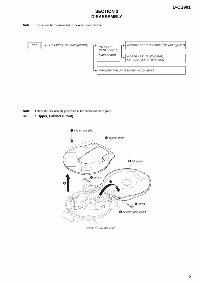
D-CS901SECTION 3
DISASSEMBLY
Note : This set can be disassembled in the order shown below.
3-1. Lid Upper, Cabinet (Front)
Note : Follow the disassembly procedure in the numerical order given.
SET
MOTOR ASSY (SLED)(M902), OPTICAL PICK-UP (DAX-25E)
MAIN BOARD
MAIN (SWITCH UNIT) BOARD, HOLD LEVER
LID UPPER, CABINET (FRONT) MD ASSY(CDM-3125ER),
MOTOR ASSY, TURN TABLE (SPINDLE)(M901)
3 five screws (B2)
1 screw
6 flexible cable (20P)
1 screw
7 lid, upper
5 cabinet (front)
42
cabinet (lower) sub assy

6
D-CS901
3-2. MD Assy (CDM-3125ER), MAIN Board
3-3. Motor Assy, Turn Table (Spindle) (M901)
4
6
RV801
cabinet (lower) sub ASSY
lever(vol)(B)
3 connector (CN502)(white) 2 connector (CN503)(black)
7 MAIN board
5 MD ASSY (CDM-3125ER)
1 flexible cable (15P)
2
motor assy, turn table(spindle) (M901)
1 three screws (B1.7x5)
chassis

7
D-CS901
3-4. Motor Assy (Sled) (M902), Optical Pick-up (DAX-25E)
3-5. MAIN (SWITCH UNIT) Board, Hold Lever
48
0
2
1 screw (B 1.7x5)
6 screw (P 1.4x3.5)
9 screw assy, feed
chassis
qa optical pick-up(DAX-25E)
7 bracket (Shaft)
gear B
3 cover, gear
5 motor assy (sled) (M902)
lid, upper
cabinet (lower) sub assy
When installing, align S904 with the cut-out of the HOLD LEVER.
When replacing the hold knob, coat here with the specified grease (SGL-601) .
4 screw (B)(1.4 × 4)
3 MAIN (SWITCH UNIT) board
5 hold lever
6 hold knob
7 O ring
1 six screws (B1.7 × 3)
2 lid, cover

8
D-CS901SECTION 4TEST MODE
The following confirmation can be performed when the Test Modeis set.
4-1. How to set the Test Mode. To set the Test Mode, the following method is available.1) Confirm the set is not powered on.2) Confirm the following settings.
CD DOOR OPEN switch (S801) ... OFFSolder Tap (TAP2 ) ... OPENHOLD switch (S804) ... OFFG-PROTECTION switch (S802) ... 1
3) Short the solder tap TAP1 (TEST) on the MAIN board.4) Turn on the main power.
4-2. How to cancel the Test Mode1) Turn off the power.2) Open the solder tap TAP1 (TEST) on the MAIN board.Note: The solder should be removed clean.• Refer to Page 10 – MAIN BOARD (side A) –
4-3. Operation when the Test Mode is set.When the Test Mode becomes active, following messages aredisplayed on the LCD.
DISPLAY
Test Modeversion display
All lit(Test Mode)
CS 032
4-4. Operations by buttons in the Test Mode. The following confirmations can be performed by operating buttons.
[Operation when a CD is not placed in the CD player]• FOLDER + / FOLDER – buttonMotion of the optical pick-up (to outside or inside)Note : Be sure to keep your eyes apart from the direct emission of
the Laser diode.Do not move the optical pick-up over outermost or innermost.
[Operation when a CD is placed in the CD player]Procedure:1) Confirm the set is not powered on.2) Keep short the solder tap TAP1 (TEST) on the MAIN board.3) After turning on the power, set a CD in the player.
Then press the >B button.Tracking/Sled servo offFocus searchSpindle servo on
DISPLAY
00 00
• x buttonAll servos (Focus/Tracking/Sled) offCLV brakeMute on
• FOLDER + / FOLDER – buttonMotion of the optical pick-up (to outside or inside)
• DISPLAY buttonError rate signal outBy each pressing the DISPLAY button error rate or spindlespeed is displayed.
DISPLAY
Err
001 00 01
• . buttonEF adjustmentCLV automatic modeTracking/Sled servo off
DISPLAY
EF00 00
• SOUND buttonAutomatic gain adjustment
DISPLAY
AUTO GA00 00
• REPEAT/ENTER buttonTracking gain up modeTracking gain normal mode (Brake off)
DISPLAY
GA UP
GA NORM
(To cancel this mode, turn off the power. Then set in the Test Modeagain.)

9
D-CS901
• PLAY MODE buttonDisplay spindle speedEvery pressing the button changes spindle speed 1 to speed 4 .Tracking/Sled servo onMute off
DISPLAY Spindle Speed
(1.5x)
(2x)
(3x)
(3.5x)
001 00 01
002 00 02
003 00 03
004 00 04
(To cancel this mode, turn off the power. Then set in the Test Modeagain.)
4-5. Error rate displayC1 error rate is displayed when the following operation areperformed during playing in the Test Mode.
1) Cancel the other Test Mode by turnig off the power.2) After turnig on the power, set a CD in the player.
Then press the >B button.
DISPLAY
00 00
3) Set the automatic gain adjustment by pressing the SOUNDbutton.
4) Press the PLAY MODE button.
DISPLAY
001 00 01 (Spindle Speed)
5) C1 error rate display mode is active by pressing the DISPLAYbutton.
The LCD displays the following message.
Value of00 00 ~ 0099 : OK01 00 ~ : NG
DISPLAY
Err
Note: Press the SOUND button before pressing the PLAY MODEbutton during playing a CD.By pressing in a wrong order, the value of Er ** ** becomesvery big.
6) When the error rate or spindle speed is displayed, the PLAYMODE button is effective and the spindle speed is changeable.
7) Press the x button to stop.8) Turn off the power.9) Open txhe solder tap TAP1 (TEST) on the MAIN board.Note: The solder should be removed clean.
4-6. Test mode for switch unit (PI LCD TEST)To set this test mode, short the solder taps TAP1(TEST) andTAP3(TEST) on the MAIN board.• Refer to Page 10 – MAIN BOARD (side A) (side B) – and Figure
10
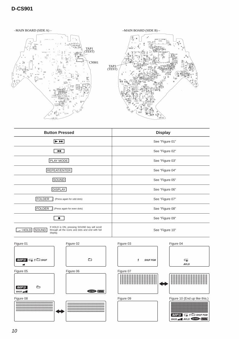
D-CS901
Button Pressed Display
PLAY MODE
See "Figure 01"
Figure 01 Figure 02 Figure 03 Figure 04
Figure 05 Figure 06 Figure 07
Figure 08 Figure 09 Figure 10 (End up like this.)
See "Figure 02"
See "Figure 03"
See "Figure 04"
See "Figure 05"
See "Figure 06"
See "Figure 07"
See "Figure 08"
See "Figure 09"
See "Figure 10"
REPEAT/ENTER
SOUND
DISPLAY
FOLDER (Press again for odd dots)
(Press again for even dots)FOLDER |
SOUNDIf HOLD is ON, pressing SOUND key will scroll through all the icons and dots and end with full display.
HOLD
TAP1(TEST)
CN901
–MAIN BOARD (SIDE A) –
IC403
IC801
IC803
IC804IC602
IC601
IC703IC701
IC402IC404
IC30
1
IC40
1
IC405
–MAIN BOARD (SIDE B) –
TAP3(TEST)
11
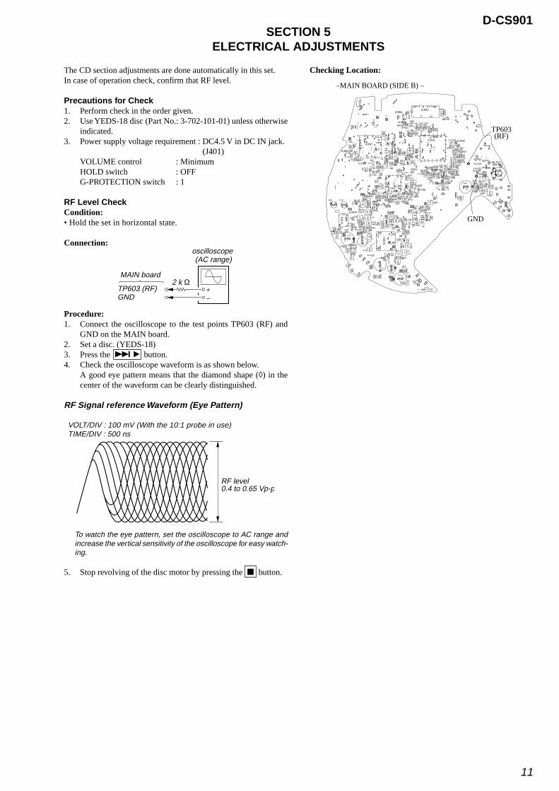
D-CS901SECTION 5
ELECTRICAL ADJUSTMENTS
The CD section adjustments are done automatically in this set.In case of operation check, confirm that RF level.
Precautions for Check1. Perform check in the order given.2. Use YEDS-18 disc (Part No.: 3-702-101-01) unless otherwise
indicated.3. Power supply voltage requirement : DC4.5 V in DC IN jack.
(J401)VOLUME control : MinimumHOLD switch : OFFG-PROTECTION switch : 1
RF Level CheckCondition:• Hold the set in horizontal state.
Connection:
Procedure:1. Connect the oscilloscope to the test points TP603 (RF) and
GND on the MAIN board.2. Set a disc. (YEDS-18)3. Press the > B button.4. Check the oscilloscope waveform is as shown below.
A good eye pattern means that the diamond shape (◊) in thecenter of the waveform can be clearly distinguished.
RF Signal reference Waveform (Eye Pattern)
VOLT/DIV : 100 mV (With the 10:1 probe in use) TIME/DIV : 500 ns
To watch the eye pattern, set the oscilloscope to AC range andincrease the vertical sensitivity of the oscilloscope for easy watch-ing.
5. Stop revolving of the disc motor by pressing the x button.
Checking Location:
oscilloscope (AC range)
+–
MAIN board
TP603 (RF)GND
2 k Ω
RF level0.4 to 0.65 Vp-p
IC801
IC803
IC804IC602
IC601
IC703IC701
IC402IC404
IC30
1
IC40
1
IC405
–MAIN BOARD (SIDE B) –
TP603(RF)
GND
12
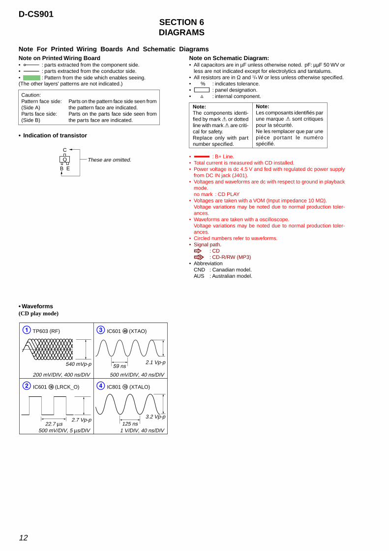
D-CS901SECTION 6DIAGRAMS
• Indication of transistor
C
B
These are omitted.
E
Q
Note on Printed Wiring Board• X : parts extracted from the component side.• Y : parts extracted from the conductor side.• : Pattern from the side which enables seeing.(The other layers' patterns are not indicated.)
Caution:Pattern face side: Parts on the pattern face side seen from(Side A) the pattern face are indicated.Parts face side: Parts on the parts face side seen from(Side B) the parts face are indicated.
Note on Schematic Diagram:• All capacitors are in µF unless otherwise noted. pF: µµF 50 WV or
less are not indicated except for electrolytics and tantalums.• All resistors are in Ω and 1/4
W or less unless otherwise specified.• % : indicates tolerance.• C : panel designation.• f : internal component.
• A : B+ Line.• Total current is measured with CD installed.• Power voltage is dc 4.5 V and fed with regulated dc power supply
from DC IN jack (J401).• Voltages and waveforms are dc with respect to ground in playback
mode.no mark : CD PLAY
• Voltages are taken with a VOM (Input impedance 10 MΩ).Voltage variations may be noted due to normal production toler-ances.
• Waveforms are taken with a oscilloscope.Voltage variations may be noted due to normal production toler-ances.
• Circled numbers refer to waveforms.• Signal path.
J : CDc : CD-R/RW (MP3)
• AbbreviationCND : Canadian model.AUS : Australian model.
Note:The components identi-fied by mark 0 or dottedline with mark 0 are criti-cal for safety.Replace only with partnumber specified.
Note:Les composants identifiés parune marque 0 sont critiquespour la sécurité.Ne les remplacer que par unepiéce portant le numérospécifié.
Note For Printed Wiring Boards And Schematic Diagrams
• Waveforms(CD play mode)
200 mV/DIV, 400 ns/DIV
500 mV/DIV, 5 µs/DIV
540 mVp-p
2 IC601 <z/n>>(LRCK_O)
22.7 µs2.7 Vp-p
1 TP603 (RF)
500 mV/DIV, 40 ns/DIV
1 V/DIV, 40 ns/DIV
4 IC801 q; (XTALO)
3 IC601 rk>(XTAO)
2.1 Vp-p
125 ns3.2 Vp-p
59 ns

1313
D-CS901
6-1. Block Diagrams– MAIN Section 1 –
• R-ch is omitted due to
same as L-ch.
• Signal path
:CD
:CD-R/RW(MP3)
86871740 465542 16
DSP_
XSOE
_O
DSP_
GRSC
OR_I
NT
DSP_
FOK_
I
DSP_
GFS_
I
DSP_
SCOR
_INT
DSP_
SENS
_I
DSP_
SCK_
O
DSP_
XLAT
_O
4041
2122
7
OPTICAL PICK-UPBLOCK
DAX-25E
AA
B
RF
E
F
B
RF
E
F
PDPD
LDLD
DETECTOR
VCC
FOCUS COIL
TRACKING COIL
FI1RI1
1718
FI2RI2
FI4
VINDET
RI4
19PWM3
20FR3
APCREF
VCC1 +2V
FO1
RO1
FO4
RO4
LGO4
INM4
RF41
PAPC
F+
F–
T+
T–
IC405COMPARATOR
SYNC
34
3526
95100
51
AMUT
E_O
82
DSP_
XQOK
_O
89
DSP_
XWRE
_O
53 96
DSP_
XRST
_O
92
32
DSP_
XRDE
_O
49
PWRS
W_O
44
BEEP
_O
MP3
_RST
_OM
P3_S
DAO(
I2C)
_OM
P3_S
CLO(
I2C)
_OM
P3ST
ANDB
Y_O
MP3
_REQ
_I
MSDTO
MSCK
IC801 (1/2)SYSTEM CONTROL
X60116.9MHz
B
C
A
38
36
26
24
69
6
2
M901SPINDLE MOTOR
FO3
RO3M
C+
C–
30
28
DRIVER
DRIVER
CONTROLLER
DRIVER
PD AMP
LD AMP
POWERSUPPLY4
APC
LEVELSHIFTER
3
IC401 (1/2)FOCUS/TRACKING COIL DRIVER, SPINDLE/SLED MOTOR DRIVER
B+ +3V4
M902SLED
MOTOR
FO2
RO2M
S+
S–
34
32
DRIVER
IC601RF AMP,
DIGITAL SIGNAL PROCESSOR,DIGITAL SERVO PROCESSOR,
D-RAM CONTROLLER
LPF
SIGNALPROCESSOR
BLOCK
MEMORYCONTROLLER,
BUS BOOSTBLOCK
SERVOBLOCK
MDS
MDP
SENS
SCORSDTO
XTAO
XRDE_I
XTAI
RFAC
XSOE
XLATCLOK
XRASXWE
XCAS
AOUT2
AOUT1
MUTE_O
XRST
_I
/RES
ET
I2CD
ATA_
II2
CCLK
_I
STAN
DBY
PO7
RFDC
BA
SFDRSRDRFFDRFRDRTFDRTRDR
D0-D3D0-D3
A0-A10A0-A10
WDCKGFS
XTAOXTAI
EF
89F
92
91
A
B
88
84
RFDC
RFAC
E
90
5423
IC602D-RAM
XRASXWEXCAS
10099
SFDRSRDR
9695
FFDRFRDR
9897
TFDRTRDR
26 2422 652320
102 MDS
103 MDP
27
SCOR
_O
104 C176
FOK_
O
XSOE
_I
GRSC
OR_O
SENS
_O
CLK_
I
XLAT
_I
69
GFS_
O
25
MUT
E_I
30
XQOK
31
XWRE
61
28
51
56
48
92
1
47
R-CH
R-CH
LIN
IC301HEADPHONE AMP
14LOUT
8
PWRSW
MUTE19
BEEP17PW SW
BEEPMT SW
20
J301
i
4, 3,6, 5
2, 3,24, 25
116-113,17-15,13-11,
117
9-12,15-19,21,8
OPGSW
OPSTB
OPGSW_OOPSTB_O
OPGSWOPSTB
1
3
4
41
DSP_
SDTO
_O21
SDT_
I
1
7
3
5
6
2
3
5
1
7
IC804BUFFER
IC803BUFFER
R-CH
9109
107
111
60
62
391
12108
14106
13110
18
7
3
IC701MP3 DECODER
PCMD_I
PCMD_O
LRCK_I
LRCK_O
BCK_I
BCK_O
45
5
47
6
1 98
19
SDO
SDI0
LRCKIA
BCKIA
CKO
XI
Q701
IC703BUFFER
1 7
3 5
6 2
VOLRV801
LASERAGCDAC_O
CLVOUTPUT_OCLVFB_I
DVDD(2V)
VOLM
NT_A
D

1414
D-CS901
– MAIN Section 2 –
+3VREG
IC802
3115
IC402DC/DC CONVERTER
23
SWITCHINGPOWER
CIRCUIT 2
SWITCHINGPOWER
CIRCUIT 3
VGPOWERCIRCUIT
CHARGECONTROL
Q417B+ SWITCH
Q401,402B+ SWITCH
Q411B+ SWITCH
Q410B+
SWITCH
Q1B+
SWITCH
INTERFACE
CLKOR OSC
AMP
BIAS
SAWTOOTHGENERATOR
STANDBYREFERENCE
Q412SWITCH
53
61
50
11
12
14
13
15
65
48
89
42
CHG ON/OFF
BANDGAPREFERENCE
(VREF)
IC801 (2/2)SYSTEM CONTROL
1
4854
XPOW
LT_O
27
CHGM
NT_A
D
WAK
EUP_
O
VCPU_2.0V
VCPU_2.0V
IC602(D-RAM)
VCC
VCC2 _2.5V
IC401 (2/2)POWER CONTROL
B+
B–
J401DC IN 4.5V
!
DTC2
VCPU
57 STNG
VLG3
VIN
CHGSW
CHGSW
DCIN
L5VG
CHARGINGBATTERYVOLTAGEDETECT
59
58
BATM260
BATM1
73
VCC274
RF378
VCC1 _2.0V
VLGO2
SYNC
VCC1
WAKEUP
CLOCK
DATA
SYNC
MSCK
MSDTO
LATCH
VREF
CHGMNT
DRY BATTERYSIZE "AA"
(IEC DESIGNATION LR6)2PCS,3V
A
BC
B+ +3VIC401
FOCUS/TRACKING COIL DRIVERSPINDLE/SLED MOTOR DRIVER,
IC301HEADPHONE AMP
D406
Q404
L406
D401
D404
L414
51
30
64777897
28
18
88
S804JOGKEY
SW7 - 12FUNCTION
KEY
90
S801(CD DOOR OPEN)
S802G-PROTECTION
1
2
S904
HOLD
OFF
ON
IC1LCD DRIVER
56-63
73767788
79-86D0 - D7 DB0-7
SEG0-60
COM0-15
A0RD
WR1LCD_RST_O
A0E(RD)R/W(RW)RES
87 VDD
JOGKEY_AD
20 JOGKEY_INT
KEY2_AD
GPRO_I
XHOLD_I
11 XTALI
10 XTALO
OPENSW_INT
D410
3.0V
IC801VDD
D411
X8018MHz
25
21
31
BATMNT_AD
DCIN_INT
DCINMNT_AD
RESETRESET
Q408
Q407
IC2
2 4D1
R24 - 28
72-12
96-100,1-11
LCD1LIQUID
CRYSTALDISPLAY
3.0V
IC404
32
IC403
Q403
13
24
RS
1515
D-CS901
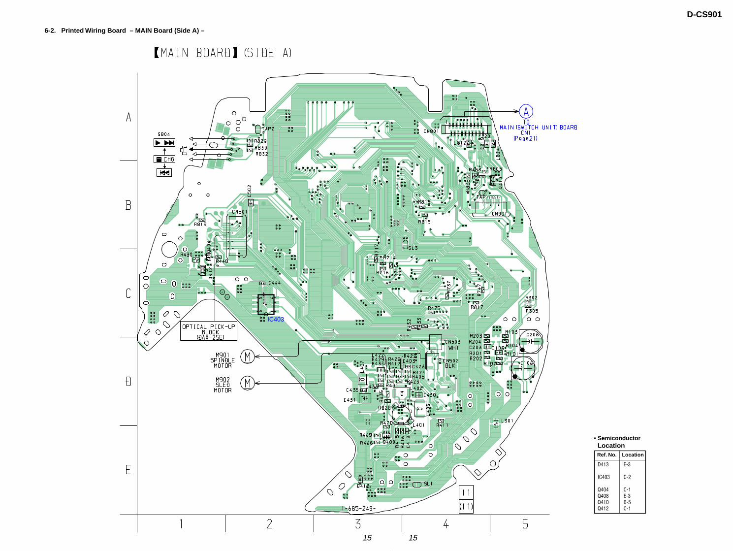
6-2. Printed Wiring Board – MAIN Board (Side A) –
IC403
(TEST)
Ref. No. Location
D413 E-3
IC403 C-2
Q404 C-1Q408 E-3Q410 B-5Q412 C-1
• SemiconductorLocation

1616
D-CS901
6-3. Printed Wiring Board – MAIN Board (Side B) –
IC801
IC802
IC803
IC804IC602
IC601
IC703IC701
IC402IC404
IC30
1
IC40
1
IC405
(TEST)TP603(RF)
GND
Ref. No. Location
D101 E-1D201 E-1D301 E-2D401 C-4D403 C-4D404 C-4D405 C-3D406 D-2D408 C-4D409 C-3D410 C-2D411 C-3D412 D-1D461 B-4D801 A-2
IC301 D-1IC401 D-2IC402 C-2IC404 C-1IC405 B-4IC601 B-3IC602 A-3IC701 C-2IC703 C-3IC801 B-2IC802 C-2IC803 B-1IC804 A-2
Q401 D-2Q402 D-1Q403 C-4Q407 D-3Q411 D-1Q417 C-3Q701 C-1
• SemiconductorLocation
1717
D-CS901
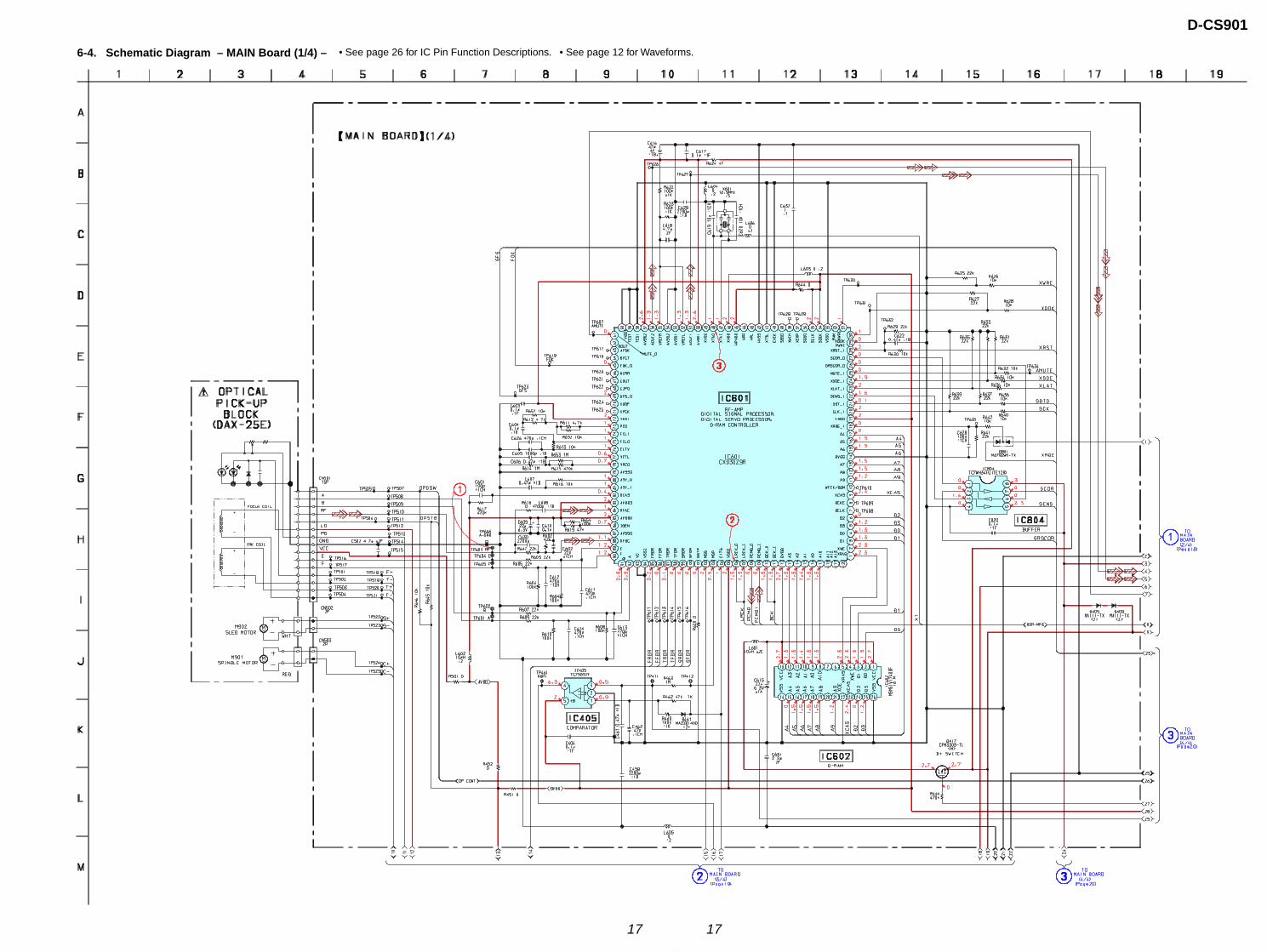
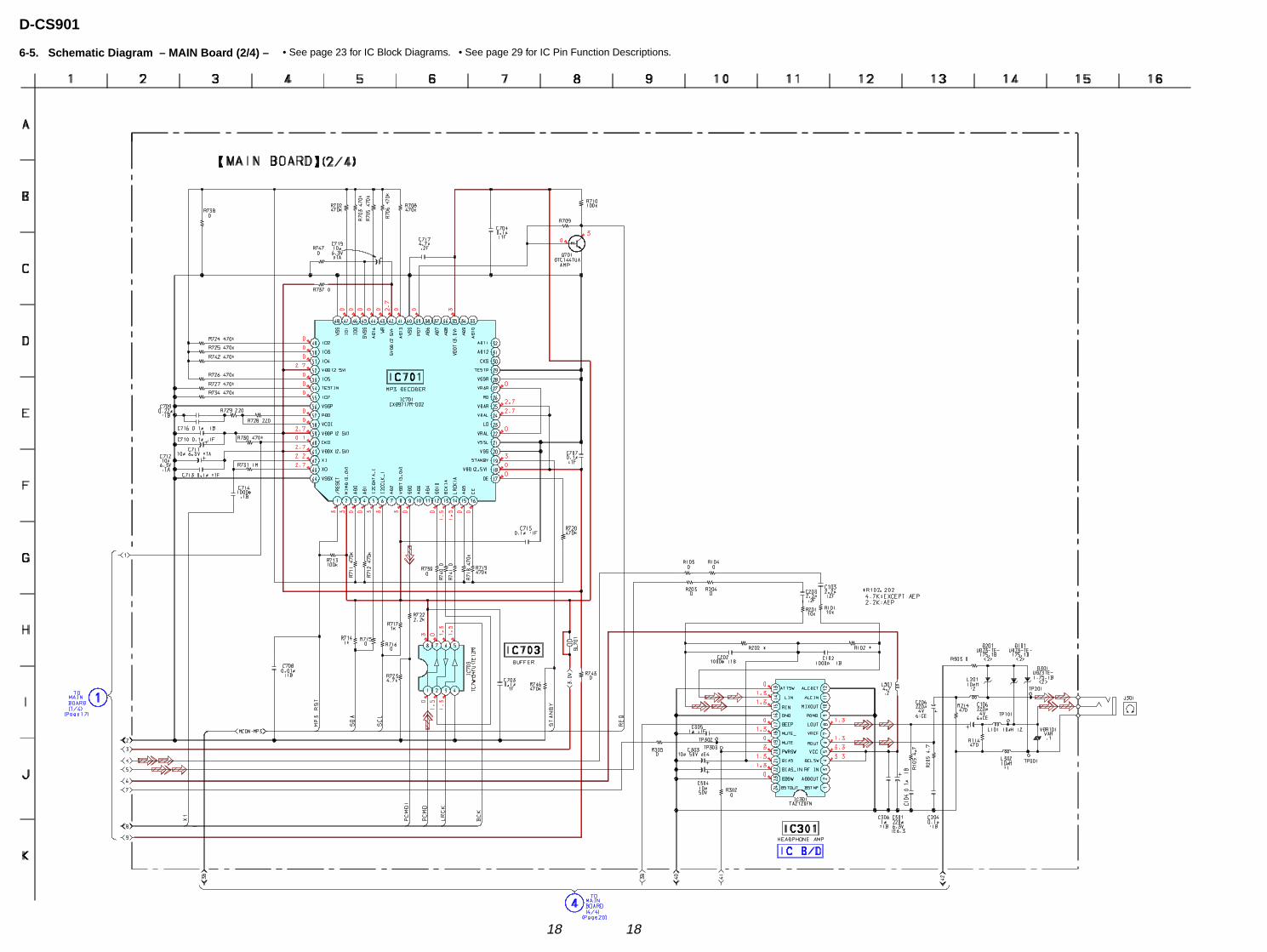
6-4. Schematic Diagram – MAIN Board (1/4) – • See page 26 for IC Pin Function Descriptions. • See page 12 for Waveforms.
1818
D-CS901
6-5. Schematic Diagram – MAIN Board (2/4) – • See page 23 for IC Block Diagrams. • See page 29 for IC Pin Function Descriptions.

1919
D-CS901
6-6. Schematic Diagram – MAIN Board (3/4) – • See page 24 for IC Pin Function Descriptions.

2020
D-CS901
6-7. Schematic Diagram – MAIN Board (4/4) – • See page 31 for IC Pin Function Descriptions. • See page 12 for Waveforms.

2121
D-CS901
6-8. Printed Wiring Board – MAIN (SWITCH UNIT) Board –
IC1
IC2
(LIQUID CRYSTAL DISPLAY)

2222
D-CS901
6-9. Schematic Diagram – MAIN (SWITCH UNIT) Board – • See page 23 for IC Block Diagrams.
It is impossible to measure the voltage of IC1.

23
D-CS901
• IC Block DiagramsIC301 TA2120FN (EL) (MAIN Board)
+ –+–+ –
23 18 17 16 15 14 13
2 3 4 5 6 7 8 9 11 121
24
BIAS BEEPPWSW
MTSW
ALCDET
ATTSW
PWCSW
ROUT LOUT
BEEPMUTE MUTE_γ
BST
PWB
PWC
BSTNF
ADDOUT
RF IN OCLSW
ROUT VREF LOUT PGND MIXOUT
ALCIN
ALCDET
ATTSWLINRINGND
PWRSWBIAS
BIASIN
BBSW
BSTOUT
VCC
ADDA
ADDB
2122
PWA
ALC ALC
20 19
10
IC1 NJU6570AC (MAIN (SWITCH UNIT) Board)

24
D-CS901
6-10. IC Pin Function Descriptions• MAIN Board IC401 TB2130AF (Coil Driver, Motor Driver, Power Control)
Pin No.
1
2
3
4
5
6
7
8
9
10
11
12
13
14
15
16
17
18
19
20
21
22
23
24
25
26
27
28
29
30
31
32
33
34
35
36
37
38
39
40
41
42
43
44
45
46
47
48
49
50
I/O
—
O
I
—
O
I
I
—
I
—
I
I
I
I
I
O
I
I
I
I
I
I
—
O
—
O
—
O
—
O
—
O
—
O
—
O
—
O
—
I
I
O
I
I
I
O
O
I
O
—
Pin Name
VREF
RF41
PAPC
VINDET
RF4
INM4
APCREF
L5
VG
GND
SYNC
WAKEUP
CLOCK
DATA
LATCH
RSTB
FI2
RI2
PWM3
FR3
FI4
RI4
VD4
RO4
MGND4
FO4
VD34
RO3
MGND3
FO3
VD23
RO2
MGND2
FO2
VD12
RO1
MGND1
FO1
VD1
FI1
RI1
CHGSW
RS1
INP1
INM1
RF1
VOUT1
DCIN
VDRAM
VCPU
Description
Reference voltage terminal
Output of the operational amplifier 1 (Power supply 4 APC)
Non-inverting input of the operational amplifier 1 (Power supply 4 APC)
VIN detect terminal
Output of the operational amplifier 2 (Power supply 4 APC)
Inverting input of the operational amplifier 2 (Power supply 4 APC)
Control voltage input (Power supply 4 APC)
Coil connection terminal for VG supply
VG supply terminal (VG=VIN+5V)
Ground
Synchronous clock input (176kHz)
WAKE UP signal input
Serial control clock input (530kHz)
Serial control data input
Serial control data latch signal input
Reset signal output
Forward signal input (the driver 2)
Reverse signal input (the driver 2)
Forward signal input (the driver 3)
Reverse signal input (the driver 3)
Forward signal input (the driver 4)
Reverse signal input (the driver 4)
Power supply (the driver 4)
Reverse signal output (the driver 4)
Ground (the driver 4)
Forward signal output (the driver 4)
Power supply (the driver 3 and 4)
Reverse signal output (the driver 3)
Ground (the driver 3)
Forward signal output (the driver 3)
Power supply (the driver 2 and 3)
Reverse signal output (the driver 2)
Ground (the driver 2)
Forward signal output (the driver 2)
Power supply (the driver 1 and 2)
Reverse signal output (the driver 1)
Ground (the driver 1)
Forward signal output (the driver 1)
Power supply (the driver 1)
Forward signal input (the driver 1)
Reverse signal input (the driver 1)
Transistor drive terminal for charging the rechargeable battery
Charge current detection terminal (Non-inverting input 2 of the error amplifier) (open)
Non-inverting input 1 of the error amplifier (Charging circuit for the rechargeable battery)
Inverting input of the error amplifier (Charging circuit for the rechargeable battery) (open)
Signal output of the error amplifier (Charging circuit for the rechargeable battery) (open)
Transistor drive terminal for VIN power supply circuit (open)
DC IN (AC adaptor) detect signal input
VDRAM output terminal (for DRAM)(= 2.0V standard) (open)
VCPU input (= 2.0V standard)

25
D-CS901
Pin No.
51
52
53
54
55
56
57
58
59
60
61
62
63
64
65
66
67
68
69
70
71
72
73
74
75
76
77
78
79
80
I/O
O
—
—
I
O
I
—
O
I
I
O
—
—
—
—
—
—
—
O
—
—
—
O
—
O
I
I
O
—
—
Pin Name
VCC1
DELAY
DTC2
INM2
RF2
INP2
STNG
CHGMNT
BATM2
BATM1
VLGO2
L2L
PGND2
L2H
VIN
L4H
PGND4
L4L
VLGO4
L3H
PGND3
L3L
VLG3
VCC2
VCC3
INP3
INM3
RF3
DTC3
DTC4
Description
VCC1 (for CD DSP) output (= 1.98V standard)
Terminal for VCC1 control time constant
Duty setting terminal (Power supply 2 VCPU)
Inverting input of the operational amplifier (Power supply 2 VCPU)
Output of the operational amplifier (Power supply 2 VCPU)
Non-inverting input of the operational amplifier (Power supply 2 VCPU)
External transistor drive terminal (Power supply 2 VCPU)
Rechargeable battery voltage detection signal output
Minus terminal of the lower rechargeable battery
Minus terminal of the upper rechargeable battery
Output of the power supply 2 VCPU (= 2.0V standard)
Coil connection terminal H (Power supply 2 VCPU)
Ground of the power supply 2 VCPU
Coil connection terminal L (Power supply 2 VCPU)
VIN input of the power supply 4 (3.3V at AC adaptor use, Non charging mode)
Coil connection terminal H (Power supply 4 VAPC)
Ground of the power supply 4 VAPC
Coil connection terminal L (Power supply 4 VAPC)
Output of the power supply 4 VAPC (= 1.8V standard)
Coil connection terminal H (Power supply 3 VDAC)
Ground of the power supply 3 VDAC
Coil connection terminal L (Power supply 3 VDAC)
Output of the power supply 3 VDAC (= 2.7V standard)
VCC2 input for VCC3 (= 2.7V standard)
Output of VCC3 VDOJ (= 2.38V standard) (open)
Inverting input of the operational amplifier 1 (Power supply 3 VDAC)
Non-inverting input of the operational amplifier 1 (Power supply 3 VDAC)
Output of the operational amplifier 1 (Power supply 3 VDAC)
Duty setting terminal (Power supply 3 VDAC)
Duty setting terminal (Power supply 4 VAPC)
26
D-CS901
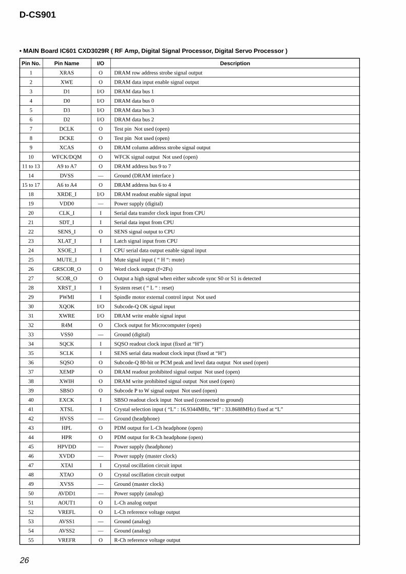
• MAIN Board IC601 CXD3029R ( RF Amp, Digital Signal Processor, Digital Servo Processor )
Pin No.
1
2
3
4
5
6
7
8
9
10
11 to 13
14
15 to 17
18
19
20
21
22
23
24
25
26
27
28
29
30
31
32
33
34
35
36
37
38
39
40
41
42
43
44
45
46
47
48
49
50
51
52
53
54
55
I/O
O
O
I/O
I/O
I/O
I/O
O
O
O
O
O
—
O
I/O
—
I
I
O
I
I
I
O
O
I
I
I/O
I/O
O
—
I
I
O
O
O
O
I
I
—
O
O
—
—
I
O
—
—
O
O
—
—
O
Pin Name
XRAS
XWE
D1
D0
D3
D2
DCLK
DCKE
XCAS
WFCK/DQM
A9 to A7
DVSS
A6 to A4
XRDE_I
VDD0
CLK_I
SDT_I
SENS_I
XLAT_I
XSOE_I
MUTE_I
GRSCOR_O
SCOR_O
XRST_I
PWMI
XQOK
XWRE
R4M
VSS0
SQCK
SCLK
SQSO
XEMP
XWIH
SBSO
EXCK
XTSL
HVSS
HPL
HPR
HPVDD
XVDD
XTAI
XTAO
XVSS
AVDD1
AOUT1
VREFL
AVSS1
AVSS2
VREFR
Description
DRAM row address strobe signal output
DRAM data input enable signal output
DRAM data bus 1
DRAM data bus 0
DRAM data bus 3
DRAM data bus 2
Test pin Not used (open)
Test pin Not used (open)
DRAM column address strobe signal output
WFCK signal output Not used (open)
DRAM address bus 9 to 7
Ground (DRAM interface )
DRAM address bus 6 to 4
DRAM readout enable signal input
Power supply (digital)
Serial data transfer clock input from CPU
Serial data input from CPU
SENS signal output to CPU
Latch signal input from CPU
CPU serial data output enable signal input
Mute signal input ( “ H “: mute)
Word clock output (f=2Fs)
Output a high signal when either subcode sync S0 or S1 is detected
System reset ( “ L “ : reset)
Spindle motor external control input Not used
Subcode-Q OK signal input
DRAM write enable signal input
Clock output for Microcomputer (open)
Ground (digital)
SQSO readout clock input (fixed at “H”)
SENS serial data readout clock input (fixed at “H”)
Subcode-Q 80-bit or PCM peak and level data output Not used (open)
DRAM readout prohibited signal output Not used (open)
DRAM write prohibited signal output Not used (open)
Subcode P to W signal output Not used (open)
SBSO readout clock input Not used (connected to ground)
Crystal selection input ( “L” : 16.9344MHz, “H” : 33.8688MHz) fixed at “L”
Ground (headphone)
PDM output for L-Ch headphone (open)
PDM output for R-Ch headphone (open)
Power supply (headphone)
Power supply (master clock)
Crystal oscillation circuit input
Crystal oscillation circuit output
Ground (master clock)
Power supply (analog)
L-Ch analog output
L-Ch reference voltage output
Ground (analog)
Ground (analog)
R-Ch reference voltage output

27
D-CS901
Pin No.
56
57
58
59
60
61
62
63
64
65
66
67
68
69
70
71
72
73
74
75
76
77
78
79
80
81
82
83
84
85
86
87
88
89
90
91
92
93
94
95
96
97
98
99
100
101
102
103
104
105
106
107
I/O
O
—
I
I
—
O
O
I/O
I/O
O
I/O
I/O
O
O
O
O
—
O
I
O
I
I
O
—
O
O
I
—
I
—
I
—
I
I
I
I
I
I
—
O
O
O
O
O
O
I
O
O
O
—
O
I
Pin Name
AOUT2
AVDD2
TES1
TEST
VSS1
MUTE_O
DOUT
ATSK
DFCT
FOK_O
MIRR
COUT
C2PO
GFS_O
XUGF
XPCK
VDD1
PCO
FILI
FILO
CLTV
VCTL
VPCO
AVSS3
ASY_0
ASY_1
BIAS
AVDD3
RFAC
AVDD0
IGEN
AVSS0
RFDC
E
F
B
A
VC
VSS2
FRDR
FFDR
TRDR
TFDR
SRDR
SFDR
SSTP
MDS
MDP
C176
VDD2
LRCK_O
LRCK_I
Description
R-Ch analog output
Power supply (analog)
Test pin (Normally connected to ground)
Test pin (Normally connected to ground)
Ground (digital)
L-Ch,R-Ch “0” detection flag (AND output)
Digital Out output terminal (open)
Anti-shock I/O Not used (open)
Defect signal I/O Not used (open)
Focus OK signal out put
Mirror signal I/O Not used (open)
Track count signal I/O Not used (open)
C2PO signal output Not used (open)
GFS signal output
XUGF signal output Not used (open)
XPCK signal output Not used (open)
Power supply (digital)
Master PLL charge pump output
Master PLL filter input
Master PLL filter output (slave = digital PLL)
Multiplier VCO1 control voltage input
Wide-band EFM PLL VCO2 control voltage input
Wide-band EFM PLL charge pump output
Ground (analog)
EFM full-swing output (“L” = VSS, “H” = VDD)
Asymmetry comparator voltage output
Asymmetry circuit constant current input
Power supply (analog)
EFM signal input
Power supply (analog)
Operational amplifier constant current input
Ground (analog)
RF signal input
E signal input
F signal input
B signal input
A signal input
Center voltage input
Ground (digital)
Focus drive output
Focus drive output
Tracking drive output
Tracking drive output
Sled drive output
Sled drive output
Disc innermost track detection signal input (connected to ground)
Spindle drive output
Spindle motor drive servo control signal output
176.4kHz output
Power supply (digital)
D/A interface LR clock output (f=Fs)
D/A interface LR clock input

28
D-CS901
Pin No.
108
109
110
111
112
113 to 116
117
118
119 to 120
I/O
O
I
O
I
—
O
O
O
O
Pin Name
PCMD_O
PCMD_I
BCK_O
BCK_I
DVDD
A3 to A0
A10
A11
A12,A13
Description
D/A interface Serial data output
D/A interface Serial data input
D/A interface Bit clock output
D/A interface Bit clock input
Power supply (DRAM interface)
DRAM address bus 3 to 0
DRAM address bus 10
DRAM address bus 11 Not used (open)
Test pin Not used (open)

29
D-CS901
• MAIN Board IC701 CXD9717R-002 (MP3 Decoder)
Pin No.
1
2
3
4
5
6
7
8
9
10
11
12
13
14
15
16
17
18
19
20
21
22
23
24
25
26
27
28
29
30
31 to 34
35
36 to 38
39
40
41
42
43
44
45
46, 47
48
49 to 51
52
53
54
55
56
57
58
59
I/O
I
I
I
I
I/O
I
O
—
O
O
O
I
I
I
I
I
I
—
I
—
—
—
O
—
—
O
—
—
I
O
O
—
O
O
—
I/O
—
I
I
—
I
—
I
—
I
I
I
—
O
I
—
Pin Name
/RESET
MIMD (3.0V)
AD0
AD1
I2CDATA_I
I2CCLK_I
AD2
VDDT (3.0V)
SDO
AD3
AD4
SDI0
BCKIA
LRCKIA
AD5
CE
OE
VDD (2.5V)
STANDBY
VSS
VSSL
VRAL
LO
VDAL
VDAR
RO
VRAR
VSSR
TESTP
CKS
AD12 to AD9
VDDT (3.0V)
AD8 to AD6
PO7
VSS
AD13
SVDD (2.5V)
WR
AD16
SVSS
IO0,IO1
VSS
IO2 to IO4
VDD (2.5V)
IO5
TESTIN
IO7
VSSP
PDO
VCOI
VDDP (2.5V)
Description
Reset input terminal “L”: reset
Microcomputer interface mode selection input “H”: I2C, “L”: TSB (fixed at “H”)
Microcomputer interface chip select signal input (fixed at “L”)
Microcomputer interface latch pulse input (fixed at “L”)
Microcomputer interface serial data input/output (SDA in I2C mode)
Microcomputer interface serial clock input (SCL in I2C mode)
Microcomputer interface acknowledge signal output (open)
Power supply (3.3V) for digital circuit
Data output
Bit clock output (open)
LR clock output (open)
Data input 0
Bit clock input A
LR clock input A
Data input 1 (fixed at “L”)
Bit clock input B (fixed at “L”)
LR clock input B (fixed at “L”)
Power supply (2.5V) for digital circuit
Standby mode control signal input “H”: STB, “L”: normal
Ground for digital circuit
Ground for DAC Lch
Reference voltage terminal for DAC Lch
DAC Lch signal output (open)
Power supply (2.5V) for DAC Lch
Power supply (2.5V) for DAC Rch
DAC Rch signal output (open)
Reference voltage terminal for DAC Rch
Ground for DAC Rch
Terminal for test “H”: test mode, “L”: normal (fixed at “L”)
SPDIF signal output (open)
Genaeral purpose output 0 to 3 (open)
Power supply (3.0V) for digital circuit
Genaeral purpose output 4 to 6 (open)
Genaeral purpose output 7 Interrupt request signal output to the system control (IC801)
Ground for digital circuit
External interrupt signal input (fixed at “L”)
Power supply (2.5V) for internal 1Mbit SRAM
Flag signal input (fixed at “L”)
Flag signal input (fixed at “L”)
Ground for internal 1Mbit SRAM
General purpose input (fixed at “L”)
Ground for digital circuit
General purpose input (fixed at “L”)
Power supply (2.5V) for digital circuit
General purpose input (fixed at “L”)
Test terminal (fixed at “L”)
Flag signal input 2 (fixed at “L”)
Ground for VCO circuit
PLL phase error detection signal output
VCO control voltage input
Power supply for VCO circuit (2.5V)
30
D-CS901
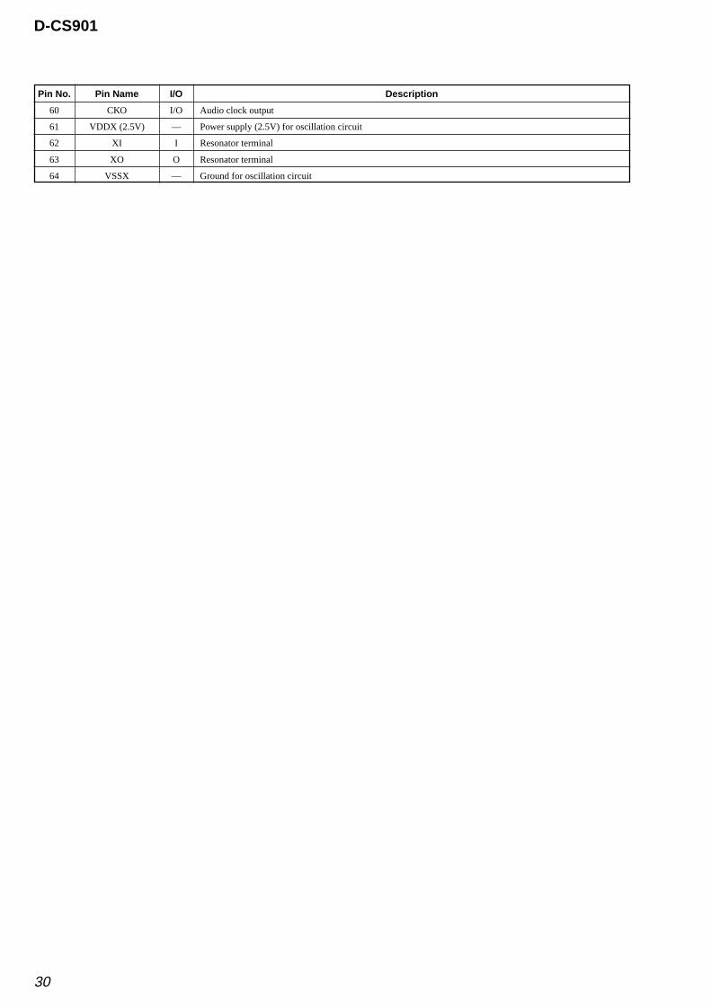
Pin No.
60
61
62
63
64
I/O
I/O
—
I
O
—
Pin Name
CKO
VDDX (2.5V)
XI
XO
VSSX
Description
Audio clock output
Power supply (2.5V) for oscillation circuit
Resonator terminal
Resonator terminal
Ground for oscillation circuit
31
D-CS901
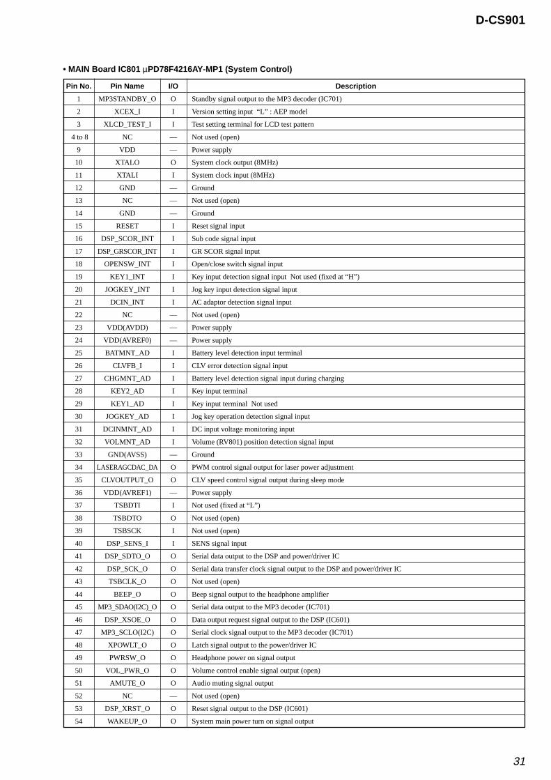
• MAIN Board IC801 µPD78F4216AY-MP1 (System Control)
Pin No.
1
2
3
4 to 8
9
10
11
12
13
14
15
16
17
18
19
20
21
22
23
24
25
26
27
28
29
30
31
32
33
34
35
36
37
38
39
40
41
42
43
44
45
46
47
48
49
50
51
52
53
54
I/O
O
I
I
—
—
O
I
—
—
—
I
I
I
I
I
I
I
—
—
—
I
I
I
I
I
I
I
I
—
O
O
—
I
O
I
I
O
O
O
O
O
O
O
O
O
O
O
—
O
O
Pin Name
MP3STANDBY_O
XCEX_I
XLCD_TEST_I
NC
VDD
XTALO
XTALI
GND
NC
GND
RESET
DSP_SCOR_INT
DSP_GRSCOR_INT
OPENSW_INT
KEY1_INT
JOGKEY_INT
DCIN_INT
NC
VDD(AVDD)
VDD(AVREF0)
BATMNT_AD
CLVFB_I
CHGMNT_AD
KEY2_AD
KEY1_AD
JOGKEY_AD
DCINMNT_AD
VOLMNT_AD
GND(AVSS)
LASERAGCDAC_DA
CLVOUTPUT_O
VDD(AVREF1)
TSBDTI
TSBDTO
TSBSCK
DSP_SENS_I
DSP_SDTO_O
DSP_SCK_O
TSBCLK_O
BEEP_O
MP3_SDAO(I2C)_O
DSP_XSOE_O
MP3_SCLO(I2C)
XPOWLT_O
PWRSW_O
VOL_PWR_O
AMUTE_O
NC
DSP_XRST_O
WAKEUP_O
Description
Standby signal output to the MP3 decoder (IC701)
Version setting input “L” : AEP model
Test setting terminal for LCD test pattern
Not used (open)
Power supply
System clock output (8MHz)
System clock input (8MHz)
Ground
Not used (open)
Ground
Reset signal input
Sub code signal input
GR SCOR signal input
Open/close switch signal input
Key input detection signal input Not used (fixed at “H”)
Jog key input detection signal input
AC adaptor detection signal input
Not used (open)
Power supply
Power supply
Battery level detection input terminal
CLV error detection signal input
Battery level detection signal input during charging
Key input terminal
Key input terminal Not used
Jog key operation detection signal input
DC input voltage monitoring input
Volume (RV801) position detection signal input
Ground
PWM control signal output for laser power adjustment
CLV speed control signal output during sleep mode
Power supply
Not used (fixed at “L”)
Not used (open)
Not used (open)
SENS signal input
Serial data output to the DSP and power/driver IC
Serial data transfer clock signal output to the DSP and power/driver IC
Not used (open)
Beep signal output to the headphone amplifier
Serial data output to the MP3 decoder (IC701)
Data output request signal output to the DSP (IC601)
Serial clock signal output to the MP3 decoder (IC701)
Latch signal output to the power/driver IC
Headphone power on signal output
Volume control enable signal output (open)
Audio muting signal output
Not used (open)
Reset signal output to the DSP (IC601)
System main power turn on signal output

32
D-CS901
Pin No.
55
56 to 63
64
65 to 71
72
73 to 75
76
77
78
79, 80
81
82
83
84, 85
86
87
88
89
90
91
92
93
94
95
96
97
98
99
100
I/O
O
I/O
O
—
—
—
—
O
O
—
—
O
O
—
I
I
I
O
I
—
O
I
—
O
O
O
I
—
O
Pin Name
DSP_XLAT_O
D0 to D7
A0
NC
GND
NC
CONF_O
LCD_RD_O
LCD_WR1_O
CONF_O
VDD
DSP_XQOK_O
LASERAGCPWM_O
CONF_O
DSP_FOK_I
DSP_GFS_I
XGPRO_I
DSP_XWRE_O
XHOLD_I
CONF_O
DSP_XRDE_O
XTESTMODE_I
GND
OPSTB_O
MP3_RST_O
LCD_RST_O
MP3_REQ_I
CONF_O
OPGSW_O
Description
Latch signal output to the DSP (IC601)
Data bus to the LCD driver (IC1)
LCD driver address control signal output
Not used (open)
Ground
Not used (open)
Not used (open)
Read control signal output to the LCD driver (IC1) (open)
WR1 signal output to the LCD driver (IC1)
Not used (open)
Power supply
ESP control write OK confirm signal output to the DSP (IC601)
AGC PWM signal output (open)
Not used (open)
Focus OK signal input from the DSP (IC601)
Guard frame signal input from the DSP (IC601)
G-protection switch signal input
ESP control write enable signal output to the DSP (IC601)
Hold switch signal input “L” : HOLD on
Not used (open)
ESP control read enable signal output to the DSP (IC601)
Test mode setting terminal “L” : CD test mode
Ground
Standby signal output to the CD mechanism deck “H” : standby mode, “L” : normal mode
MP3 reset signal output to the MP3 decoder (IC701)
Reset signal output to the LCD driver (IC1)
Request interface signal input from the MP3 decoder (IC701)
Not used (open)
Optical pick-up RF gain control signal output

33
D-CS901
• The mechanical parts with no reference num-ber in the exploded views are not supplied.
• Accessories are given in the last of the electri-cal parts list.
NOTE:• -XX and -X mean standardized parts, so they
may have some difference from the originalone.
• Items marked “*” are not stocked since theyare seldom required for routine service. Somedelay should be anticipated when orderingthese items.
The components identified by mark 0 ordotted line with mark 0 are critical for safety.Replace only with part number specified.
Les composants identifiés par une marque0 sont critiques pour la sécurité.Ne les remplacer que par une pièce portantle numéro spécifié.
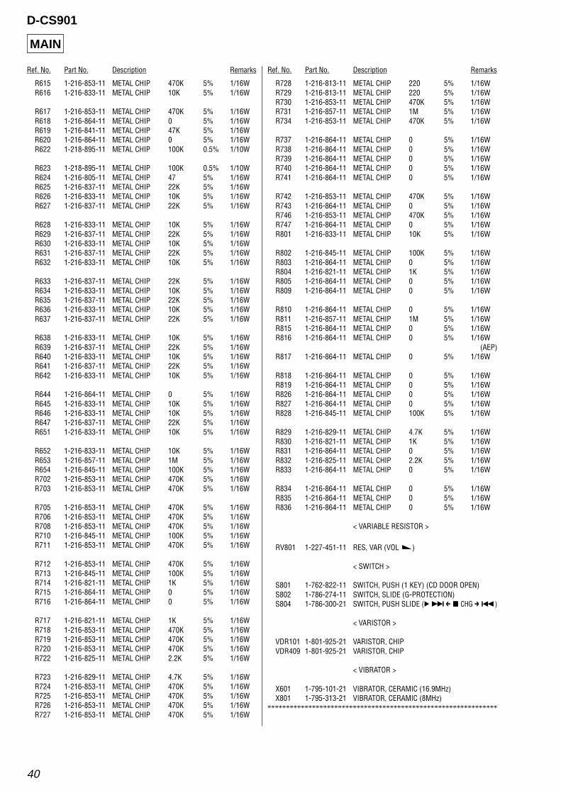
Ref. No. Part No. Description Remarks Ref. No. Part No. Description Remarks
6-1. Upper Lid Section
222
233
14
15
22
1
11
10
12
13
18
17
5
64
7
8
9
LCD1
1921
cabinet section
16
13
2
2
a
a
SECTION 7EXPLODED VIEWS
1 3-242-903-01 LID, COVER2 3-343-254-31 SCREW (B1.7X3), TAPPING3 X-3382-276-1 RUBBER (DISPLAY) SUB ASSY4 1-685-277-11 MAIN (SWITCH UNIT) BOARD5 X-3382-275-1 RUBBER (OPERATE) SUB ASSY
6 3-242-895-01 BUTTON (OPERATE)7 3-242-898-01 WINDOW, LCD8 3-318-201-51 SCREW (B) (1.4X4), TAPPING9 3-238-008-01 LEVER (HOLD)10 3-242-899-01 LID, UPPER
11 3-221-329-01 RING, O12 3-238-021-01 KNOB (HOLD)
13 3-238-478-01 SCREW14 3-242-900-01 GRIP15 3-238-013-01 ARM (A)16 3-238-025-01 PACKING (UPPER LID)17 3-243-429-01 SHEET, ADHESIVE
18 3-243-507-01 RUBBER, CONNECTOR19 3-242-902-01 HOLDER, LCD21 3-243-094-01 BUTTON, FOLDER22 3-242-901-01 PAD, ELASTOMER23 3-242-897-01 BUTTON (DISPLAY)
LCD1 1-804-786-11 LCD

34
D-CS901
Ref. No. Part No. Description Remarks Ref. No. Part No. Description Remarks
6-2. Cabinet Section
51 3-237-999-01 CABINET (FRONT)52 3-238-001-01 LID, BATTERY CASE53 3-238-014-01 ARM (B)54 4-908-792-51 SCREW (B2)55 3-343-254-31 SCREW (B1.7X3), TAPPING
56 1-824-119-11 CABLE, FLEXIBLE57 4-223-609-01 KNOB (JOGGABLE)58 X-3382-335-1 BUCKLE SUB ASSY59 4-225-316-01 ROLLER
52
51
57 5663
60
61
54
55
53
cabinet lower section
Optical Pick-Up section(CDM-3125ER)
54
6264
66
59
58
not supplied
BT402
BT400
BT401
60 3-221-309-01 LEVER (VOL) (A)61 4-223-413-01 SCREW (M1.4X3)62 3-338-687-21 SCREW (M1.4X2), TAPPING
* 63 A-3178-748-A MAIN BOARD, COMPLETE (EXCEPT AEP)* 63 A-3178-753-A MAIN BOARD, COMPLETE (AEP)
64 X-3381-670-1 BRACKET (ROLLER) ASSYBT400 3-238-476-01 TERMINAL (+), BATTERYBT401 3-238-477-01 TERMINAL BOARD (RELAY),BATTERYBT402 3-221-307-01 TERMINAL BOARD (-), BATTERY

35
D-CS901
Ref. No. Part No. Description Remarks Ref. No. Part No. Description Remarks
6-3. Cabinet Lower Section
105113
108
105
115
112
105
111
101102 103
107
109
105 106
104
105103
110
114
not supplied
101 3-238-023-01 BUTTON (JOG)102 3-238-017-01 RUBBER103 3-318-201-51 SCREW (B) (1.4X4), TAPPING104 3-238-016-01 JOG105 4-908-792-31 SCREW (B2)
106 3-238-010-01 SHEET, ADHESIVE107 3-238-019-01 PLATE (JOG)108 3-238-002-11 STRAP, BRACKET
109 3-238-020-01 PLATE (JOG)110 3-221-310-01 LEVER (VOL) (B)111 X-3382-334-1 CABINET (LOWER) SUB ASSY112 3-238-015-01 PLATE, ORNAMENTAL113 3-221-311-11 PACKING (H/P)
114 3-221-329-01 RING, O115 3-238-007-01 KNOB (VOL)

36
D-CS901
6-4. Optical Pick-up Section (CDM-3125ER)
M901
M902
151
152
152
153
154
155
156
156156
157
158
159
160
164
161
162163
Ref. No. Part No. Description Remarks Ref. No. Part No. Description Remarks
151 4-218-821-01 COVER, GEAR152 3-318-203-71 SCREW (B1.7X5), TAPPING153 A-3052-902-A FEED ASSY, SCREW154 4-218-823-01 GEAR (B)155 4-218-825-01 SPRING, SLED
156 4-222-765-01 INSULATOR157 3-235-420-01 CHASSIS158 4-218-827-01 RETAINER, SHAFT
159 3-686-458-03 SCREW (P1.4X3.5), TAPPING0160 X-3380-950-1 OPTCAL PICK-UP (DAX-25E)
161 3-235-418-01 RACK162 3-348-998-81 SCREW (M1.4)163 4-220-645-01 SHAFT, STANDARD
164 3-243-233-01 SPACER, CDMM901 A-3052-904-A MOTOR ASSY, TURN TABLE (SPINDLE)M902 A-3328-627-A MOTOR ASSY, SLED (SLED)
The components identified bymark 0 or dotted line with mark0 are critical for safety.Replace only with part numberspecified.
Les composants identifiés parune marque 0 sont critiquespour la sécurité.Ne les remplacer que par unepièce portant le numéro spécifié.

37
D-CS901
NOTE:• Due to standardization, replacements in the
parts list may be different from the parts speci-fied in the diagrams or the components usedon the set.
• -XX and -X mean standardized parts, so theymay have some difference from the originalone.
• RESISTORSAll resistors are in ohms.METAL: Metal-film resistor.METAL OXIDE: Metal oxide-film resistor.F: nonflammable
• Items marked “*” are not stocked since theyare seldom required for routine service.Some delay should be anticipated when order-ing these items.
• SEMICONDUCTORSIn each case, u: µ, for example:uA. . : µA. . uPA. . : µPA. .uPB. . : µPB. . uPC. . : µPC. .uPD. . : µPD. .
• CAPACITORSuF: µF
• COILSuH: µH
When indicating parts by reference number,please include the board name.
The components identified by mark 0 ordotted line with mark 0 are critical for safety.Replace only with part number specified.
Les composants identifiés par une marque0 sont critiques pour la sécurité.Ne les remplacer que par une pièce portantle numéro spécifié.
• AbbreviationCND : Canadian model.AUS : Australian model.
Ref. No. Part No. Description Remarks Ref. No. Part No. Description Remarks
MAINSECTION 8
ELECTRICAL PARTS LIST
* A-3178-748-A MAIN BOARD, COMPLETE (EXCEPT AEP)* A-3178-753-A MAIN BOARD, COMPLETE (AEP)
*********************
< BATTERY TERMINAL >
BT400 3-238-476-01 TERMINAL (+), BATTERYBT401 3-238-477-01 TERMINAL BOARD (RELAY),BATTERYBT402 3-221-307-01 TERMINAL BOARD (–), BATTERY
< CAPACITOR >
C102 1-162-964-11 CERAMIC CHIP 0.001uF 10% 50VC103 1-164-505-11 CERAMIC CHIP 2.2uF 16VC104 1-107-826-11 CERAMIC CHIP 0.1uF 10.00% 16VC106 1-113-690-11 ELECT CHIP 220uF 20.00% 4VC202 1-162-964-11 CERAMIC CHIP 0.001uF 10% 50V
C203 1-164-505-11 CERAMIC CHIP 2.2uF 16VC204 1-107-826-11 CERAMIC CHIP 0.1uF 10.00% 16VC206 1-113-690-11 ELECT CHIP 220uF 20.00% 4VC301 1-126-369-11 ELECT 220uF 20% 6.3VC303 1-124-261-00 ELECT 10uF 20% 50V
C304 1-124-261-00 ELECT 10uF 20% 50VC305 1-115-156-11 CERAMIC CHIP 1uF 10VC306 1-125-837-91 CERAMIC CHIP 1uF 10% 6.3VC401 1-162-970-11 CERAMIC CHIP 0.01uF 10% 25VC403 1-162-968-11 CERAMIC CHIP 0.0047uF 10% 50V
C404 1-164-156-11 CERAMIC CHIP 0.1uF 25VC406 1-135-259-11 TANTAL. CHIP 10uF 20.00% 6.3VC407 1-125-837-91 CERAMIC CHIP 1uF 10% 6.3VC409 1-124-584-00 ELECT 100uF 20% 10VC410 1-124-635-00 ELECT 220uF 20.00% 6.3V
C411 1-162-970-11 CERAMIC CHIP 0.01uF 10% 25VC412 1-124-635-00 ELECT 220uF 20.00% 6.3VC413 1-162-970-11 CERAMIC CHIP 0.01uF 10% 25VC414 1-162-966-11 CERAMIC CHIP 0.0022uF 10% 50VC415 1-164-156-11 CERAMIC CHIP 0.1uF 25V
C416 1-164-156-11 CERAMIC CHIP 0.1uF 25VC417 1-110-569-21 TANTAL. CHIP 47uF 20.00% 4VC418 1-126-369-11 ELECT 220uF 20% 6.3VC420 1-135-259-11 TANTAL. CHIP 10uF 20.00% 6.3VC421 1-110-569-21 TANTAL. CHIP 47uF 20.00% 4V
C422 1-125-837-91 CERAMIC CHIP 1uF 10% 6.3VC423 1-162-970-11 CERAMIC CHIP 0.01uF 10% 25VC424 1-165-176-11 CERAMIC CHIP 0.047uF 10.00% 16VC425 1-115-156-11 CERAMIC CHIP 1uF 10VC426 1-125-837-91 CERAMIC CHIP 1uF 10% 6.3V
C427 1-164-156-11 CERAMIC CHIP 0.1uF 25VC428 1-115-156-11 CERAMIC CHIP 1uF 10VC429 1-125-837-91 CERAMIC CHIP 1uF 10% 6.3VC430 1-117-720-11 CERAMIC CHIP 4.7uF 10VC431 1-135-259-11 TANTAL. CHIP 10uF 20.00% 6.3V
C433 1-162-968-11 CERAMIC CHIP 0.0047uF 10% 50VC434 1-135-259-11 TANTAL. CHIP 10uF 20.00% 6.3VC435 1-107-826-11 CERAMIC CHIP 0.1uF 10.00% 16VC436 1-110-569-11 TANTAL. CHIP 47uF 20.00% 6.3VC437 1-115-467-11 CERAMIC CHIP 0.22uF 10.00% 10V
C440 1-104-913-11 TANTAL. CHIP 10uF 20.00% 16VC441 1-117-720-11 CERAMIC CHIP 4.7uF 10VC444 1-115-156-11 CERAMIC CHIP 1uF 10VC445 1-115-467-11 CERAMIC CHIP 0.22uF 10.00% 10VC446 1-162-964-11 CERAMIC CHIP 0.001uF 10% 50V
C447 1-164-315-11 CERAMIC CHIP 470PF 5.00% 50VC448 1-124-635-00 ELECT 220uF 20.00% 6.3VC450 1-125-837-91 CERAMIC CHIP 1uF 10% 6.3VC451 1-125-891-11 CERAMIC CHIP 0.47uF 10.00% 10VC453 1-115-156-11 CERAMIC CHIP 1uF 10V
C456 1-110-569-11 TANTAL. CHIP 47uF 20.00% 6.3VC458 1-162-966-11 CERAMIC CHIP 0.0022uF 10% 50VC460 1-164-505-11 CERAMIC CHIP 2.2uF 16VC461 1-125-891-11 CERAMIC CHIP 0.47uF 10.00% 10VC462 1-162-923-11 CERAMIC CHIP 47PF 5% 50V
C467 1-110-569-11 TANTAL. CHIP 47uF 20.00% 6.3VC469 1-135-259-11 TANTAL. CHIP 10uF 20.00% 6.3VC502 1-117-720-11 CERAMIC CHIP 4.7uF 10VC601 1-162-927-11 CERAMIC CHIP 100PF 5% 50VC602 1-162-919-11 CERAMIC CHIP 22PF 5% 50V
C603 1-164-156-11 CERAMIC CHIP 0.1uF 25VC604 1-107-826-11 CERAMIC CHIP 0.1uF 10.00% 16VC605 1-162-964-11 CERAMIC CHIP 0.001uF 10% 50VC606 1-125-891-11 CERAMIC CHIP 0.47uF 10.00% 10VC607 1-125-891-11 CERAMIC CHIP 0.47uF 10.00% 10V
C608 1-162-968-11 CERAMIC CHIP 0.0047uF 10% 50VC609 1-119-750-11 TANTAL. CHIP 22uF 20.00% 6.3VC610 1-164-156-11 CERAMIC CHIP 0.1uF 25VC611 1-164-315-11 CERAMIC CHIP 470PF 5.00% 50VC612 1-164-315-11 CERAMIC CHIP 470PF 5.00% 50V
C613 1-164-315-11 CERAMIC CHIP 470PF 5.00% 50VC614 1-164-315-11 CERAMIC CHIP 470PF 5.00% 50VC615 1-119-750-11 TANTAL. CHIP 22uF 20.00% 6.3VC616 1-110-569-21 TANTAL. CHIP 47uF 20.00% 4VC617 1-164-156-11 CERAMIC CHIP 0.1uF 25V

Ref. No. Part No. Description Remarks Ref. No. Part No. Description Remarks
38
D-CS901
MAIN
C618 1-117-720-11 CERAMIC CHIP 4.7uF 10VC619 1-162-915-11 CERAMIC CHIP 10PF 0.5PF 50VC620 1-162-915-11 CERAMIC CHIP 10PF 0.5PF 50VC622 1-125-891-11 CERAMIC CHIP 0.47uF 10.00% 10VC626 1-164-315-11 CERAMIC CHIP 470PF 5.00% 50V
C628 1-162-927-11 CERAMIC CHIP 100PF 5% 50VC629 1-162-966-11 CERAMIC CHIP 0.0022uF 10% 50VC630 1-162-966-11 CERAMIC CHIP 0.0022uF 10% 50VC631 1-164-505-11 CERAMIC CHIP 2.2uF 16VC632 1-115-156-11 CERAMIC CHIP 1uF 10V
C703 1-164-156-11 CERAMIC CHIP 0.1uF 25VC704 1-164-156-11 CERAMIC CHIP 0.1uF 25VC707 1-164-156-11 CERAMIC CHIP 0.1uF 25VC708 1-162-970-11 CERAMIC CHIP 0.01uF 10% 25VC709 1-115-467-11 CERAMIC CHIP 0.22uF 10.00% 10V
C710 1-164-156-11 CERAMIC CHIP 0.1uF 25VC711 1-135-259-11 TANTAL. CHIP 10uF 20.00% 6.3VC712 1-135-259-11 TANTAL. CHIP 10uF 20.00% 6.3VC713 1-164-156-11 CERAMIC CHIP 0.1uF 25VC714 1-162-964-11 CERAMIC CHIP 0.001uF 10% 50V
C715 1-164-156-11 CERAMIC CHIP 0.1uF 25VC716 1-107-826-11 CERAMIC CHIP 0.1uF 10.00% 16VC717 1-117-720-11 CERAMIC CHIP 4.7uF 10VC719 1-135-259-11 TANTAL. CHIP 10uF 20.00% 6.3VC801 1-164-156-11 CERAMIC CHIP 0.1uF 25V
C802 1-164-156-11 CERAMIC CHIP 0.1uF 25VC803 1-164-156-11 CERAMIC CHIP 0.1uF 25VC804 1-164-156-11 CERAMIC CHIP 0.1uF 25VC806 1-164-156-11 CERAMIC CHIP 0.1uF 25VC807 1-125-837-91 CERAMIC CHIP 1uF 10% 6.3V
C808 1-164-156-11 CERAMIC CHIP 0.1uF 25VC809 1-135-259-11 TANTAL. CHIP 10uF 20.00% 6.3VC810 1-164-156-11 CERAMIC CHIP 0.1uF 25VC811 1-162-970-11 CERAMIC CHIP 0.01uF 10% 25VC812 1-107-826-11 CERAMIC CHIP 0.1uF 10.00% 16V
C813 1-164-156-11 CERAMIC CHIP 0.1uF 25VC814 1-125-837-91 CERAMIC CHIP 1uF 10% 6.3VC815 1-164-156-11 CERAMIC CHIP 0.1uF 25VC817 1-125-837-91 CERAMIC CHIP 1uF 10% 6.3VC818 1-164-156-11 CERAMIC CHIP 0.1uF 25V
C819 1-125-837-91 CERAMIC CHIP 1uF 10% 6.3VC820 1-164-156-11 CERAMIC CHIP 0.1uF 25V
< CONNECTOR >
* CN501 1-816-237-21 CONNECTOR 15PCN502 1-784-342-21 HOUSING, CONNECTOR 2PCN503 1-784-342-11 HOUSING, CONNECTOR 2P
* CN801 1-750-504-21 CONNECTOR, FFC/FPC (ZIF) 20P
< DIODE >
D101 8-719-069-54 DIODE UDZSTE-175.1BD201 8-719-069-54 DIODE UDZSTE-175.1BD301 8-719-069-54 DIODE UDZSTE-175.1BD401 8-719-085-43 DIODE MA2YD2300LS0D403 8-719-069-54 DIODE UDZSTE-175.1B
D404 8-719-085-43 DIODE MA2YD2300LS0D405 8-719-404-50 DIODE MA111-TXD406 8-719-071-87 DIODE MA785-(TX),SO
D408 8-719-069-54 DIODE UDZSTE-175.1BD409 8-719-404-50 DIODE MA111-TX
D410 8-719-072-70 DIODE MA2ZD14001S0D411 8-719-072-70 DIODE MA2ZD14001S0D412 8-719-069-54 DIODE UDZSTE-175.1BD413 8-719-421-27 DIODE MA728-TXD461 8-719-072-70 DIODE MA2ZD14001S0
D801 8-719-044-74 DIODE MA792WK-TX
< FERRITE BEAD >
FB801 1-216-295-91 SHORT CHIP 0
< IC >
IC301 8-759-681-65 IC TA2120FN(EL)IC401 6-702-261-01 IC TB2130AFIC402 6-700-465-01 IC XC6383A301MRIC403 6-701-712-01 IC SI-3010XS-TLIC404 8-759-655-46 IC XC62FP3002MR
IC405 8-759-594-55 IC TC75S57F(TE85R)IC601 8-752-410-68 IC CXD3029RIC602 6-700-195-01 IC MSM51V17400F-10TK-FSIC701 6-702-068-01 IC CXD9717R-002IC703 8-759-679-05 IC TC7WH34FU(TE12R)
IC801 6-801-999-01 IC 784216AY-MP1IC802 6-700-466-01 IC XC61CC2102MRIC803 8-759-679-05 IC TC7WH34FU(TE12R)IC804 8-759-679-05 IC TC7WH34FU(TE12R)
< JACK >
J301 1-778-224-31 JACK (SMALL TYPE) (WATERPROOF) (i)J401 1-778-153-21 JACK,DC(POLARITY UNIFIED TYPE) (DC IN 4.5V)
< COIL >
L101 1-469-570-21 INDUCTOR 10uHL201 1-469-570-21 INDUCTOR 10uHL301 1-216-308-00 METAL CHIP 4.7 5% 1/10WL302 1-469-570-21 INDUCTOR 10uHL401 1-419-188-21 INDUCTOR 100uH
L402 1-414-434-11 INDUCTOR 100uHL403 1-400-145-21 INDUCTOR 47uHL404 1-414-404-41 INDUCTOR 100uHL405 1-414-404-41 INDUCTOR 100uHL406 1-400-144-21 INDUCTOR 22uH
L407 1-414-398-11 INDUCTOR 10uHL408 1-414-398-11 INDUCTOR 10uHL409 1-414-398-11 INDUCTOR 10uHL410 1-414-398-11 INDUCTOR 10uHL411 1-412-056-11 INDUCTOR 4.7uH
L412 1-414-392-21 INDUCTOR 1uHL413 1-414-398-11 INDUCTOR 10uHL413 1-469-967-21 INDUCTOR 10uHL414 1-414-434-11 INDUCTOR 100uHL601 1-469-967-21 INDUCTOR 10uH
L602 1-469-570-21 INDUCTOR 10uHL603 1-216-295-91 SHORT CHIP 0L604 1-216-295-91 SHORT CHIP 0L605 1-216-295-91 SHORT CHIP 0

Ref. No. Part No. Description Remarks Ref. No. Part No. Description Remarks
39
D-CS901
MAIN
L606 1-216-295-91 SHORT CHIP 0
L812 1-400-202-21 INDUCTOR 4.7uHL824 1-400-202-21 INDUCTOR 4.7uH
< TRANSISTOR >
Q401 8-729-054-79 TRANSISTOR 2SB167900LSOQ402 8-729-231-74 TRANSISTOR 2SC4116GL-TE85LQ403 8-729-921-73 TRANSISTOR 2SD1781K-T146-QRQ404 8-729-028-26 TRANSISTOR 2SK1829(TE85L)Q407 8-729-427-83 TRANSISTOR XP6501-(TX).SO
Q408 8-729-427-83 TRANSISTOR XP6501-(TX).SOQ410 8-729-047-36 TRANSISTOR CPH3303-TLQ411 8-729-047-36 TRANSISTOR CPH3303-TLQ412 6-550-071-01 TRANSISTOR 2SB169300LSOQ417 8-729-047-36 TRANSISTOR CPH3303-TL
Q701 8-729-029-15 TRANSISTOR DTC144TUA-T106
< RESISTOR >
R101 1-216-833-11 METAL CHIP 10K 5% 1/16WR102 1-216-829-11 METAL CHIP 4.7K 5% 1/16W
(EXCEPT AEP)R102 1-216-825-11 METAL CHIP 2.2K 5% 1/16W
(AEP)R103 1-216-864-11 METAL CHIP 0 5% 1/16WR104 1-216-864-11 METAL CHIP 0 5% 1/16W
R105 1-216-793-11 RES-CHIP 4.7 5% 1/10WR114 1-216-817-11 METAL CHIP 470 5% 1/16WR201 1-216-833-11 METAL CHIP 10K 5% 1/16WR202 1-216-829-11 METAL CHIP 4.7K 5% 1/16W
(EXCEPT AEP)R202 1-216-825-11 METAL CHIP 2.2K 5% 1/16W
(AEP)
R203 1-216-864-11 METAL CHIP 0 5% 1/16WR204 1-216-864-11 METAL CHIP 0 5% 1/16WR205 1-216-793-11 RES-CHIP 4.7 5% 1/10WR214 1-216-817-11 METAL CHIP 470 5% 1/16WR302 1-216-864-11 METAL CHIP 0 5% 1/16W
R303 1-216-864-11 METAL CHIP 0 5% 1/16WR305 1-216-864-11 METAL CHIP 0 5% 1/16WR401 1-216-861-11 METAL CHIP 2.2M 5% 1/16WR402 1-218-895-11 METAL CHIP 100K 0.5% 1/10WR403 1-218-895-11 METAL CHIP 100K 0.5% 1/10W
R404 1-218-903-11 METAL CHIP 220K 0.5% 1/10WR405 1-216-833-11 METAL CHIP 10K 5% 1/16WR406 1-216-841-11 METAL CHIP 47K 5% 1/16WR407 1-216-845-11 METAL CHIP 100K 5% 1/16WR408 1-216-845-11 METAL CHIP 100K 5% 1/16W
R411 1-216-864-11 METAL CHIP 0 5% 1/16WR412 1-216-821-11 METAL CHIP 1K 5% 1/16WR414 1-216-853-11 METAL CHIP 470K 5% 1/16WR415 1-216-833-11 METAL CHIP 10K 5% 1/16WR416 1-216-857-11 METAL CHIP 1M 5% 1/16W
R417 1-216-829-11 METAL CHIP 4.7K 5% 1/16WR420 1-216-864-11 METAL CHIP 0 5% 1/16WR421 1-216-857-11 METAL CHIP 1M 5% 1/16WR422 1-216-833-11 METAL CHIP 10K 5% 1/16WR423 1-216-837-11 METAL CHIP 22K 5% 1/16W
R424 1-216-833-11 METAL CHIP 10K 5% 1/16WR425 1-216-857-11 METAL CHIP 1M 5% 1/16WR426 1-216-857-11 METAL CHIP 1M 5% 1/16WR427 1-216-853-11 METAL CHIP 470K 5% 1/16WR428 1-216-833-11 METAL CHIP 10K 5% 1/16W
R429 1-216-853-11 METAL CHIP 470K 5% 1/16WR430 1-216-041-00 METAL CHIP 470 5% 1/10WR431 1-216-864-11 METAL CHIP 0 5% 1/16WR432 1-216-864-11 METAL CHIP 0 5% 1/16WR433 1-216-864-11 METAL CHIP 0 5% 1/16W
R434 1-216-849-11 METAL CHIP 220K 5% 1/16WR435 1-218-887-11 METAL CHIP 47K 0.5% 1/10WR436 1-216-849-11 METAL CHIP 220K 5% 1/16WR437 1-216-849-11 METAL CHIP 220K 5% 1/16WR438 1-216-845-11 METAL CHIP 100K 5% 1/16W
R439 1-216-853-11 METAL CHIP 470K 5% 1/16WR440 1-216-845-11 METAL CHIP 100K 5% 1/16WR441 1-216-864-11 METAL CHIP 0 5% 1/16WR442 1-218-887-11 METAL CHIP 47K 0.5% 1/10WR443 1-216-864-11 METAL CHIP 0 5% 1/16W
R444 1-216-853-11 METAL CHIP 470K 5% 1/16WR446 1-216-864-11 METAL CHIP 0 5% 1/16WR447 1-216-298-00 METAL CHIP 2.2 5% 1/10WR448 1-216-298-00 METAL CHIP 2.2 5% 1/10WR449 1-216-793-11 RES-CHIP 4.7 5% 1/10W
R450 1-216-797-11 METAL CHIP 10 5% 1/16WR451 1-216-864-11 METAL CHIP 0 5% 1/16WR452 1-216-864-11 METAL CHIP 0 5% 1/16WR453 1-216-853-11 METAL CHIP 470K 5% 1/16WR454 1-216-864-11 METAL CHIP 0 5% 1/16W
R459 1-216-864-11 METAL CHIP 0 5% 1/16WR460 1-218-895-11 METAL CHIP 100K 0.5% 1/10WR461 1-216-864-11 METAL CHIP 0 5% 1/16WR462 1-218-887-11 METAL CHIP 47K 0.5% 1/10WR463 1-216-857-11 METAL CHIP 1M 5% 1/16W
R468 1-216-857-11 METAL CHIP 1M 5% 1/16WR469 1-216-857-11 METAL CHIP 1M 5% 1/16WR470 1-216-853-11 METAL CHIP 470K 5% 1/16WR471 1-216-833-11 METAL CHIP 10K 5% 1/16WR472 1-216-837-11 METAL CHIP 22K 5% 1/16W
R473 1-216-833-11 METAL CHIP 10K 5% 1/16WR474 1-216-837-11 METAL CHIP 22K 5% 1/16WR475 1-216-833-11 METAL CHIP 10K 5% 1/16WR476 1-216-837-11 METAL CHIP 22K 5% 1/16WR501 1-216-864-11 METAL CHIP 0 5% 1/16W
R602 1-216-841-11 METAL CHIP 47K 5% 1/16WR603 1-216-837-11 METAL CHIP 22K 5% 1/16WR604 1-216-845-11 METAL CHIP 100K 5% 1/16WR605 1-216-837-11 METAL CHIP 22K 5% 1/16WR606 1-216-845-11 METAL CHIP 100K 5% 1/16W
R607 1-216-837-11 METAL CHIP 22K 5% 1/16WR608 1-216-845-11 METAL CHIP 100K 5% 1/16WR609 1-216-837-11 METAL CHIP 22K 5% 1/16WR610 1-216-845-11 METAL CHIP 100K 5% 1/16WR611 1-216-829-11 METAL CHIP 4.7K 5% 1/16W
R612 1-216-829-11 METAL CHIP 4.7K 5% 1/16WR613 1-216-833-11 METAL CHIP 10K 5% 1/16WR614 1-216-857-11 METAL CHIP 1M 5% 1/16W
Ref. No. Part No. Description Remarks Ref. No. Part No. Description Remarks
40
D-CS901
MAIN
R615 1-216-853-11 METAL CHIP 470K 5% 1/16WR616 1-216-833-11 METAL CHIP 10K 5% 1/16W
R617 1-216-853-11 METAL CHIP 470K 5% 1/16WR618 1-216-864-11 METAL CHIP 0 5% 1/16WR619 1-216-841-11 METAL CHIP 47K 5% 1/16WR620 1-216-864-11 METAL CHIP 0 5% 1/16WR622 1-218-895-11 METAL CHIP 100K 0.5% 1/10W
R623 1-218-895-11 METAL CHIP 100K 0.5% 1/10WR624 1-216-805-11 METAL CHIP 47 5% 1/16WR625 1-216-837-11 METAL CHIP 22K 5% 1/16WR626 1-216-833-11 METAL CHIP 10K 5% 1/16WR627 1-216-837-11 METAL CHIP 22K 5% 1/16W
R628 1-216-833-11 METAL CHIP 10K 5% 1/16WR629 1-216-837-11 METAL CHIP 22K 5% 1/16WR630 1-216-833-11 METAL CHIP 10K 5% 1/16WR631 1-216-837-11 METAL CHIP 22K 5% 1/16WR632 1-216-833-11 METAL CHIP 10K 5% 1/16W
R633 1-216-837-11 METAL CHIP 22K 5% 1/16WR634 1-216-833-11 METAL CHIP 10K 5% 1/16WR635 1-216-837-11 METAL CHIP 22K 5% 1/16WR636 1-216-833-11 METAL CHIP 10K 5% 1/16WR637 1-216-837-11 METAL CHIP 22K 5% 1/16W
R638 1-216-833-11 METAL CHIP 10K 5% 1/16WR639 1-216-837-11 METAL CHIP 22K 5% 1/16WR640 1-216-833-11 METAL CHIP 10K 5% 1/16WR641 1-216-837-11 METAL CHIP 22K 5% 1/16WR642 1-216-833-11 METAL CHIP 10K 5% 1/16W
R644 1-216-864-11 METAL CHIP 0 5% 1/16WR645 1-216-833-11 METAL CHIP 10K 5% 1/16WR646 1-216-833-11 METAL CHIP 10K 5% 1/16WR647 1-216-837-11 METAL CHIP 22K 5% 1/16WR651 1-216-833-11 METAL CHIP 10K 5% 1/16W
R652 1-216-833-11 METAL CHIP 10K 5% 1/16WR653 1-216-857-11 METAL CHIP 1M 5% 1/16WR654 1-216-845-11 METAL CHIP 100K 5% 1/16WR702 1-216-853-11 METAL CHIP 470K 5% 1/16WR703 1-216-853-11 METAL CHIP 470K 5% 1/16W
R705 1-216-853-11 METAL CHIP 470K 5% 1/16WR706 1-216-853-11 METAL CHIP 470K 5% 1/16WR708 1-216-853-11 METAL CHIP 470K 5% 1/16WR710 1-216-845-11 METAL CHIP 100K 5% 1/16WR711 1-216-853-11 METAL CHIP 470K 5% 1/16W
R712 1-216-853-11 METAL CHIP 470K 5% 1/16WR713 1-216-845-11 METAL CHIP 100K 5% 1/16WR714 1-216-821-11 METAL CHIP 1K 5% 1/16WR715 1-216-864-11 METAL CHIP 0 5% 1/16WR716 1-216-864-11 METAL CHIP 0 5% 1/16W
R717 1-216-821-11 METAL CHIP 1K 5% 1/16WR718 1-216-853-11 METAL CHIP 470K 5% 1/16WR719 1-216-853-11 METAL CHIP 470K 5% 1/16WR720 1-216-853-11 METAL CHIP 470K 5% 1/16WR722 1-216-825-11 METAL CHIP 2.2K 5% 1/16W
R723 1-216-829-11 METAL CHIP 4.7K 5% 1/16WR724 1-216-853-11 METAL CHIP 470K 5% 1/16WR725 1-216-853-11 METAL CHIP 470K 5% 1/16WR726 1-216-853-11 METAL CHIP 470K 5% 1/16WR727 1-216-853-11 METAL CHIP 470K 5% 1/16W
R728 1-216-813-11 METAL CHIP 220 5% 1/16WR729 1-216-813-11 METAL CHIP 220 5% 1/16WR730 1-216-853-11 METAL CHIP 470K 5% 1/16WR731 1-216-857-11 METAL CHIP 1M 5% 1/16WR734 1-216-853-11 METAL CHIP 470K 5% 1/16W
R737 1-216-864-11 METAL CHIP 0 5% 1/16WR738 1-216-864-11 METAL CHIP 0 5% 1/16WR739 1-216-864-11 METAL CHIP 0 5% 1/16WR740 1-216-864-11 METAL CHIP 0 5% 1/16WR741 1-216-864-11 METAL CHIP 0 5% 1/16W
R742 1-216-853-11 METAL CHIP 470K 5% 1/16WR743 1-216-864-11 METAL CHIP 0 5% 1/16WR746 1-216-853-11 METAL CHIP 470K 5% 1/16WR747 1-216-864-11 METAL CHIP 0 5% 1/16WR801 1-216-833-11 METAL CHIP 10K 5% 1/16W
R802 1-216-845-11 METAL CHIP 100K 5% 1/16WR803 1-216-864-11 METAL CHIP 0 5% 1/16WR804 1-216-821-11 METAL CHIP 1K 5% 1/16WR805 1-216-864-11 METAL CHIP 0 5% 1/16WR809 1-216-864-11 METAL CHIP 0 5% 1/16W
R810 1-216-864-11 METAL CHIP 0 5% 1/16WR811 1-216-857-11 METAL CHIP 1M 5% 1/16WR815 1-216-864-11 METAL CHIP 0 5% 1/16WR816 1-216-864-11 METAL CHIP 0 5% 1/16W
(AEP)R817 1-216-864-11 METAL CHIP 0 5% 1/16W
R818 1-216-864-11 METAL CHIP 0 5% 1/16WR819 1-216-864-11 METAL CHIP 0 5% 1/16WR826 1-216-864-11 METAL CHIP 0 5% 1/16WR827 1-216-864-11 METAL CHIP 0 5% 1/16WR828 1-216-845-11 METAL CHIP 100K 5% 1/16W
R829 1-216-829-11 METAL CHIP 4.7K 5% 1/16WR830 1-216-821-11 METAL CHIP 1K 5% 1/16WR831 1-216-864-11 METAL CHIP 0 5% 1/16WR832 1-216-825-11 METAL CHIP 2.2K 5% 1/16WR833 1-216-864-11 METAL CHIP 0 5% 1/16W
R834 1-216-864-11 METAL CHIP 0 5% 1/16WR835 1-216-864-11 METAL CHIP 0 5% 1/16WR836 1-216-864-11 METAL CHIP 0 5% 1/16W
< VARIABLE RESISTOR >
RV801 1-227-451-11 RES, VAR (VOL w)
< SWITCH >
S801 1-762-822-11 SWITCH, PUSH (1 KEY) (CD DOOR OPEN)S802 1-786-274-11 SWITCH, SLIDE (G-PROTECTION)S804 1-786-300-21 SWITCH, PUSH SLIDE (B > C x CHG c .)
< VARISTOR >
VDR101 1-801-925-21 VARISTOR, CHIPVDR409 1-801-925-21 VARISTOR, CHIP
< VIBRATOR >
X601 1-795-101-21 VIBRATOR, CERAMIC (16.9MHz)X801 1-795-313-21 VIBRATOR, CERAMIC (8MHz)
**************************************************************

Ref. No. Part No. Description Remarks Ref. No. Part No. Description Remarks
41
D-CS901
* 1-685-277-11 MAIN (SWITCH UNIT) BOARD************************
< CAPACITOR >
C1 1-164-156-11 CERAMIC CHIP 0.1uF 25VC3 1-162-964-11 CERAMIC CHIP 0.001uF 10% 50VC4 1-125-837-91 CERAMIC CHIP 1uF 10% 6.3VC5 1-115-156-11 CERAMIC CHIP 1uF 10VC6 1-164-156-11 CERAMIC CHIP 0.1uF 25V
C8 1-115-156-11 CERAMIC CHIP 1uF 10V
< DIODE >
D1 8-719-070-20 DIODE RB706F-40
< IC >
IC1 6-630-015-01 IC NJU6570ACIC2 8-759-177-66 IC TC7S14FU-TE85L
< JUMPER RESISTOR >
JR1 1-216-296-11 SHORT CHIP 0JR3 1-216-296-11 SHORT CHIP 0JR4 1-216-296-11 SHORT CHIP 0JR5 1-216-864-11 METAL CHIP 0 5% 1/16W
JR6 1-216-296-11 SHORT CHIP 0
< TRANSISTOR >
Q1 8-729-054-79 TRANSISTOR 2SB167900LSO
< RESISTOR >
R1 1-216-861-11 METAL CHIP 2.2M 5% 1/16WR6 1-216-821-11 METAL CHIP 1K 5% 1/16WR7 1-216-825-11 METAL CHIP 2.2K 5% 1/16WR8 1-216-829-11 METAL CHIP 4.7K 5% 1/16WR9 1-216-833-11 METAL CHIP 10K 5% 1/16W
R10 1-216-837-11 METAL CHIP 22K 5% 1/16WR12 1-216-833-11 METAL CHIP 10K 5% 1/16WR13 1-216-845-11 METAL CHIP 100K 5% 1/16WR19 1-216-857-11 METAL CHIP 1M 5% 1/16WR22 1-216-833-11 METAL CHIP 10K 5% 1/16W
R24 1-216-841-11 METAL CHIP 47K 5% 1/16WR25 1-216-841-11 METAL CHIP 47K 5% 1/16WR26 1-216-841-11 METAL CHIP 47K 5% 1/16WR27 1-216-841-11 METAL CHIP 47K 5% 1/16WR28 1-216-841-11 METAL CHIP 47K 5% 1/16W
R31 1-216-864-11 METAL CHIP 0 5% 1/16WR32 1-216-864-11 METAL CHIP 0 5% 1/16WR33 1-216-864-11 METAL CHIP 0 5% 1/16WR34 1-216-864-11 METAL CHIP 0 5% 1/16WR35 1-216-864-11 METAL CHIP 0 5% 1/16W
R36 1-216-864-11 METAL CHIP 0 5% 1/16WR37 1-216-864-11 METAL CHIP 0 5% 1/16WR38 1-216-864-11 METAL CHIP 0 5% 1/16W
< SWITCH >
S904 1-762-078-11 SWITCH, SLIDE ( HOLD)
< SWITCH >
SW7 1-771-053-21 SWITCH, KEY BOARD (DISPLAY)SW8 1-771-053-21 SWITCH, KEY BOARD (PLAY MODE)SW9 1-771-053-21 SWITCH, KEY BOARD (SOUND)SW10 1-771-053-21 SWITCH, KEY BOARD (REPEAT/ENTER)SW11 1-771-053-21 SWITCH, KEY BOARD (FOLDER+)
SW12 1-771-053-21 SWITCH, KEY BOARD (FOLDER–)
< VARISTOR >
VDR1 1-801-925-21 VARISTOR, CHIPVDR2 1-801-925-21 VARISTOR, CHIPVDR3 1-801-925-21 VARISTOR, CHIP
**************************************************************
MISCELLANEOUS***************
56 1-824-119-11 CABLE, FLEXIBLE0160 X-3380-950-1 OPTCAL PICK-UP (DAX-25E)
LCD1 1-804-786-11 LCDM901 A-3052-904-A MOTOR ASSY, TURN TABLE (SPINDLE)M902 A-3328-627-A MOTOR ASSY, SLED (SLED)
**************************************************************
ACCESSORIES************
0 1-476-845-11 ADAPTOR, AC (AC-ES455) (AEP)0 1-476-848-11 ADAPTOR, AC (AC-ES455) (UK)0 1-476-851-11 ADAPTOR, AC (AC-ES455) (US,CND)
3-240-556-01 HAND STRAP3-243-807-11 MANUAL, INSTRUCTION (SPANISH) (AEP)
3-243-807-21 MANUAL, INSTRUCTION (ENGLISH)(CND,AEP,UK)
3-243-807-31 MANUAL, INSTRUCTION (FRENCH) (CND,AEP)3-243-807-41 MANUAL, INSTRUCTION (DUTCH) (AEP)3-243-807-51 MANUAL, INSTRUCTION (SWEDISH) (AEP)3-243-807-61 MANUAL, INSTRUCTION (PORTUGUESE) (AEP)
3-243-807-71 MANUAL, INSTRUCTION (GERMAN) (AEP)3-243-807-81 MANUAL, INSTRUCTION (ITALIAN) (AEP)3-243-807-91 MANUAL, INSTRUCTION (FINNISH) (AEP)3-243-809-11 MANUAL, INSTRUCTION (ENGLISH) (US)8-953-284-95 RECEIVER,EAR MDR-W014LP/WK SET
(US,CND,AUS)
8-954-008-94 RECEIVER MDR-E808LP/WC SET (AEP,UK)
The components identified bymark 0 or dotted line with mark0 are critical for safety.Replace only with part numberspecified.
Les composants identifiés parune marque 0 sont critiquespour la sécurité.Ne les remplacer que par unepièce portant le numéro spécifié.
MAIN (SWITCH UNIT)
D-CS901
REVISION HISTORY
Clicking the version allows you to jump to the revised page.Also, clicking the version at the upper right on the revised page allows you to jump to the next revisedpage.
Ver. Date Description of Revision
1.0 2002.06 New