CYW20732A0 Single-Chip Bluetooth Low-Energy Only SoC Sheets/Cypress PDFs/CYW20732… · CYW20732A0...
35
CYW20732A0 Single-Chip Bluetooth Low-Energy Only SoC Cypress Semiconductor Corporation • 198 Champion Court • San Jose, CA 95134-1709 • 408-943-2600 Document Number: 002-14837 Rev. *L Revised November 2, 2016 The Cypress CYW20732A0 is a Bluetooth Low-Energy (BLE)-only SoC. The CYW20732A0 radio has been designed to provide low power, low cost, and robust communications for applications operating in the globally available 2.4 GHz unlicensed Industrial, Scien- tific, and Medical (ISM) band. The single-chip BLE SoC is a monolithic component implemented in a standard digital CMOS process and requires minimal external components to make a fully compliant Bluetooth device. The CYW20732A0 is available in a 32-pin, 5 mm × 5 mm 32-QFN package. Cypress Part Numbering Scheme Cypress is converting the acquired IoT part numbers from Broadcom to the Cypress part numbering scheme. Due to this conversion, there is no change in form, fit, or function as a result of offering the device with Cypress part number marking. The table provides Cypress ordering part number that matches an existing IoT part number. Features ■ Bluetooth Low-Energy (BLE)-compliant ■ Infrared modulator ■ IR learning ■ Supports Adaptive Frequency Hopping ■ Excellent receiver sensitivity ■ 10-bit auxiliary ADC with nine analog channels ■ On-chip support for serial peripheral interface (master and slave modes) ■ Cypress CypressSerial Control (BSC) interface (compatible with NXP I 2 C slaves) ■ Programmable output power control ■ Integrated ARM Cortex-M3 based microprocessor core ■ On-chip power-on reset (POR) ■ Support for EEPROM and serial flash interfaces ■ Integrated Low DropOut (LDO) regulator ■ On-chip, software controlled power management unit ■ 32-pin 32-QFN (5 mm × 5 mm) package ■ RoHS compliant Applications The following profiles are supported in ROM: ■ Battery status ■ Blood pressure monitor ■ Find me ■ Heart rate monitor ■ Proximity ■ Thermometer ■ Weight scale ■ Time Additional profiles that can be supported from RAM include: ■ Blood glucose monitor ■ Temperature alarm ■ Location Full qualification and use of these profiles may require firmware updates from Cypress. Some profiles are under development/ approval at Bluetooth SIG and conformity with the final approved version is pending. Contact your supplier for updates and the latest list of profiles. Table 1. Mapping Table for Part Number between Broadcom and Cypress Broadcom Part Number Cypress Part Number BCM20732 CYW20732 BCM20732A0KML2G CYW20732A0KML2G
Transcript of CYW20732A0 Single-Chip Bluetooth Low-Energy Only SoC Sheets/Cypress PDFs/CYW20732… · CYW20732A0...

CYW20732A0
Single-ChipBluetooth Low-Energy Only SoC
Cypress Semiconductor Corporation • 198 Champion Court • San Jose, CA 95134-1709 • 408-943-2600Document Number: 002-14837 Rev. *L Revised November 2, 2016
The Cypress CYW20732A0 is a Bluetooth Low-Energy (BLE)-only SoC. The CYW20732A0 radio has been designed to provide low power, low cost, and robust communications for applications operating in the globally available 2.4 GHz unlicensed Industrial, Scien-tific, and Medical (ISM) band.The single-chip BLE SoC is a monolithic component implemented in a standard digital CMOS process and requires minimal external components to make a fully compliant Bluetooth device. The CYW20732A0 is available in a 32-pin, 5 mm × 5 mm 32-QFN package.
Cypress Part Numbering Scheme
Cypress is converting the acquired IoT part numbers from Broadcom to the Cypress part numbering scheme. Due to this conversion, there is no change in form, fit, or function as a result of offering the device with Cypress part number marking. The table provides Cypress ordering part number that matches an existing IoT part number.
Features
Bluetooth Low-Energy (BLE)-compliant
Infrared modulator
IR learning
Supports Adaptive Frequency Hopping
Excellent receiver sensitivity
10-bit auxiliary ADC with nine analog channels
On-chip support for serial peripheral interface (master and slave modes)
Cypress CypressSerial Control (BSC) interface (compatible with NXP I2C slaves)
Programmable output power control
Integrated ARM Cortex-M3 based microprocessor core
On-chip power-on reset (POR)
Support for EEPROM and serial flash interfaces
Integrated Low DropOut (LDO) regulator
On-chip, software controlled power management unit
32-pin 32-QFN (5 mm × 5 mm) package
RoHS compliant
Applications
The following profiles are supported in ROM:
Battery status
Blood pressure monitor
Find me
Heart rate monitor
Proximity
Thermometer
Weight scale
Time
Additional profiles that can be supported from RAM include:
Blood glucose monitor
Temperature alarm
Location
Full qualification and use of these profiles may require firmware updates from Cypress. Some profiles are under development/approval at Bluetooth SIG and conformity with the final approved version is pending. Contact your supplier for updates and the latest list of profiles.
Table 1. Mapping Table for Part Number between Broadcom and Cypress
Broadcom Part Number Cypress Part Number
BCM20732 CYW20732
BCM20732A0KML2G CYW20732A0KML2G

Document Number: 002-14837 Rev. *L Page 2 of 35
CYW20732A0
Figure 1. Functional Block Diagram
IoT Resources
Cypress provides a wealth of data at http://www.cypress.com/internet-things-iot to help you to select the right IoT device for your design, and quickly and effectively integrate the device into your design. Cypress provides customer access to a wide range of information, including technical documentation, schematic diagrams, product bill of materials, PCB layout information, and software updates. Customers can acquire technical documentation and software from the Cypress Support Community website (http://community.cypress.com/).
ProcessingUnit
(ARM -CM3)
System Bus
BluetoothBaseband
Core
2.4 GHzRadio
RF Controland Data
T/RSwitch
RF I/O
GPIOControl/Status
Registers
FrequencySynthesizer
24 MHzRef Xtal
PMU
I/O Ring Bus
I/O Ring Control
Registers
PeripheralInterface
Block
1.2V VDD_COREDomain
VDD_IODomain
WAKE
1.2VLDO 1.425V to 3.6V
1.62V to 3.6V
1.2V
VDD_CORE
320KROM 60K
RAM
BSC/SPIMaster
Interface(BSC is I2C -compa ble)
SDA/MOSI
SCL/SCK
High CurrentDriver Controls
14 GPIOs
32 kHzLPCLK
9 ADCInputs
24MHz
hclk (24 MHz to 1 MHz)
AutoCal
MISO
1.2V VDD_RFDomain PWM
WDT
128 kHzLPO
÷ 4
32 kHzLPCLK
128 kHzLPCLK
32 kHz
Power
1.62V to 3.6VVDD_IO
1.2VPOR
1.2V
TestUART
IRI/O
IRMod.and
Learning
SPIM/S
3.6VMIA POR
28 ADCInputs
CT ADC
VSS,VDDO,VDDC
PeriphUART
UART_RXD
UART_TXD TxRx
RTS_NCTS_N
Muxed on GPIO
Volt. Trans

Document Number: 002-14837 Rev. *L Page 3 of 35
CYW20732A0
Contents
1. Functional Description ................................................. 41.1 Bluetooth Baseband Core ..................................... 41.2 Infrared Modulator ................................................. 51.3 Infrared Learning ................................................... 51.4 ADC Port ............................................................... 61.5 Serial Peripheral Interface ..................................... 61.6 Microprocessor Unit .............................................. 71.7 Integrated Radio Transceiver ................................ 81.8 Peripheral Transport Unit ...................................... 91.9 Clock Frequencies ............................................... 101.10 GPIO Port .......................................................... 121.11 PWM .................................................................. 121.12 Power Management Unit ................................... 13
2. Pin Assignments ........................................................ 152.1 Pin Descriptions .................................................. 152.2 Ball Maps ............................................................. 19
3. Specifications ............................................................. 203.1 Electrical Characteristics ..................................... 203.2 RF Specifications ................................................ 233.3 Timing and AC Characteristics ............................ 243.4 ESD Test Models ................................................ 27
4. Mechanical Information ............................................. 295. Ordering Information .................................................. 31A. Appendix: Acronyms and Abbreviations ................ 32 Document History .......................................................... 33

Document Number: 002-14837 Rev. *L Page 4 of 35
CYW20732A0
1. Functional Description
1.1 Bluetooth Baseband Core
The Bluetooth Baseband Core (BBC) implements all of the time-critical functions required for high performance Bluetooth operation. The BBC manages the buffering, segmentation, and data routing for all connections. It also buffers data that passes through it, handles data flow control, schedules ACL TX/RX transactions, monitors Bluetooth slot usage, optimally segments and packages data into baseband packets, manages connection status indicators, and composes and decodes HCI packets. In addition to these functions, it independently handles HCI event types and HCI command types.
The following transmit and receive functions are also implemented in the BBC hardware to increase TX/RX data reliability and security before sending over the air:
Receive Functions: symbol timing recovery, data deframing, forward error correction (FEC), header error control (HEC), cyclic redundancy check (CRC), data decryption, and data dewhitening.
Transmit Functions: data framing, FEC generation, HEC generation, CRC generation, link key generation, data encryption, and data whitening.
1.1.1 Frequency Hopping Generator
The frequency hopping sequence generator selects the correct hopping channel number depending on the link controller state, Bluetooth clock, and device address.
1.1.2 E0 Encryption
The encryption key and the encryption engine are implemented using dedicated hardware to reduce software complexity and provide minimal processor intervention.
1.1.3 Link Control Layer
The link control layer is part of the Bluetooth link control functions that are implemented in dedicated logic in the link control unit (LCU). This layer consists of the Command Controller, which takes software commands, and other controllers that are activated or configured by the Command Controller to perform the link control tasks. Each task performs a different Bluetooth link controller state. STANDBY and CONNECTION are the two major states. In addition, there are five substates: page, page scan, inquiry, and inquiry scan.
1.1.4 Adaptive Frequency Hopping
The CYW20732 gathers link quality statistics on a channel-by-channel basis to facilitate channel assessment and channel map selection. The link quality is determined by using both RF and baseband signal processing to provide a more accurate frequency hop map.
1.1.5 Bluetooth Low Energy Profiles
The CYW20732 supports Bluetooth low-energy, including the following profiles that are supported1 in ROM:
Battery status
Blood pressure monitor
Find me
Heart rate monitor
Proximity
Thermometer
Weight scale
Time
The following additional profiles can be supported1 from RAM:
Blood glucose monitor
Temperature alarm
Location
Custom profile
1. Full qualification and use of these profiles may require firmware updates from Cypress. Some of these profiles are under development/approval at the Bluetooth SIGand conformity with the final approved version is pending. Contact your supplier for updates and the latest list of profiles.

Document Number: 002-14837 Rev. *L Page 5 of 35
CYW20732A0
1.1.6 Test Mode Support
The CYW20732 fully supports Bluetooth Test mode, as described in the Bluetooth low energy specification.
1.2 Infrared Modulator
The CYW20732 includes hardware support for infrared TX. The hardware can transmit both modulated and un-modulated waveforms. For modulated waveforms, hardware inserts the desired carrier frequency into all IR transmissions. IR TX can be sourced from firmware-supplied descriptors, a programmable bit, or the peripheral UART transmitter.
If descriptors are used, they include IR on/off state and the duration between 1 and 32,767 µsec. The CYW20732 IR TX firmware driver inserts this information in a hardware FIFO and makes sure that all descriptors are played out without a glitch due to under run (see Figure 2 on page 5).
Figure 2. Infrared TX
1.3 Infrared Learning
The CYW20732 includes hardware support for infrared learning. The hardware can detect both modulated and unmodulated signals. For modulated signals, the CYW20732 can detect carrier frequencies between 10 kHz– 500 kHz and the duration that the signal is present or absent. The CYW20732 firmware driver supports further analysis and compression of learned signal. The learned signal can then be played back through the CYW20732 IR TX subsystem (see Figure 3).
Figure 3. Infrared RX

Document Number: 002-14837 Rev. *L Page 6 of 35
CYW20732A0
1.4 ADC Port
The CYW20732 contains a 16-bit ADC (effective number of bits is 10).
Additionally:
There are nine analog input channels in the 32-pin package
The following GPIOs can be used as ADC inputs: P0 P1 P8/P33 (select only one) P11 P12 P13/P28 (select only one) P14/P38 (select only one) P15 P32
The conversion time is 10 μs.
There is a built-in reference with supply- or bandgap-based reference modes.
The maximum conversion rate is 187 kHz.
There is a rail-to-rail input swing.
The ADC consists of an analog ADC core that performs the actual analog-to-digital conversion and digital hardware that processes the output of the ADC core into valid ADC output samples. Directed by the firmware, the digital hardware also controls the input multiplexers that select the ADC input signal Vinp and the ADC reference signals Vref.
The ADC input range is selectable by firmware control:
When an input range of 0–3.6V is used, the input impedance is 3 MΩ.
When an input range of 0–2.4V is used, the input impedance is 1.84 MΩ.
When an input range of 0–1.2V is used, the input impedance is 680 kΩ.
ADC modes are defined in Table 2.
1.5 Serial Peripheral Interface
The CYW20732 has two independent SPI interfaces. One is a master-only interface and the other can be either a master or a slave. Each interface has a 16-byte transmit buffer and a 16-byte receive buffer. To support more flexibility for user applications, the CYW20732 has optional I/O ports that can be configured individually and separately for each functional pin as shown in Table 3, Table 4, and Table 5. The CYW20732 acts as a SPI master device that supports 1.8V or 3.3V SPI slaves. The CYW20732 can also act as an SPI slave device that supports a 1.8V or 3.3V SPI master.
Table 2. ADC Modes
Mode ENOB (Typical) Maximum Sampling Rate (kHz) Latencya (μs)
a.Settling time after switching channels.
0 13 5.859 171
1 12.6 11.7 85
2 12 46.875 21
3 11.5 93.75 11
4 10 187 5

Document Number: 002-14837 Rev. *L Page 7 of 35
CYW20732A0
1.6 Microprocessor Unit
The CYW20732 microprocessor unit (µPU) executes software from the link control (LC) layer up to the application layer components. The microprocessor is based on an ARM Cortex-M3, 32-bit RISC processor with embedded ICE-RT debug and JTAG interface units. The µPU has 320 KB of ROM for program storage and boot-up, 60 KB of RAM for scratch-pad data, and patch RAM code. The SoC has a total storage of 380 KB, including RAM and ROM.
The internal boot ROM provides power-on reset flexibility, which enables the same device to be used in different HID applications with an external serial EEPROM or with an external serial flash memory. At power-up, the lowest layer of the protocol stack is executed from the internal ROM memory.
External patches may be applied to the ROM-based firmware to provide flexibility for bug fixes and feature additions. The device can also support the integration of user applications.
1.6.1 EEPROM Interface
The CYW20732 provides a Cypress Serial Control (CSC) master interface. BSC is programmed by the CPU to generate four types of bus transfers: read-only, write-only, combined read/write, and combined write/read. BSC supports both low-speed and fast mode devices. BSC is compatible with an NXP I2C slave device, except that master arbitration (multiple I2C masters contending for the bus) is not supported.
The EEPROM can contain customer application configuration information including application code, configuration data, patches, pairing information, BD_ADDR, baud rate, SDP service record, and file system information used for code.
Native support for the Microchip 24LC128, Microchip 24AA128, and the STMicroelectronics M24128-BR is included.
1.6.2 Serial Flash Interface
The CYW20732 includes an SPI master controller that can be used to access serial flash memory. The SPI master contains an AHB slave interface, transmit and receive FIFOs, and the SPI core PHY logic.
Table 3. CYW20732 First SPI Set (Master Mode)
Pin Name SPI_CLK SPI_MOSI SPI_MISO SPI_CSa
a. Any GPIO can be used as SPI_CS when SPI is in master mode.
Configured Pin Name SCL SDA P24 –
– – P26 –
– – P32 –
Table 4. CYW20732 Second SPI Set (Master Mode)
Pin Name SPI_CLK SPI_MOSI SPI_MISO SPI_CSa
a. Any GPIO can be used as SPI_CS when SPI is in master mode.
Configured Pin Name P3 P0 P1 –
– P4 P25 –
P24 P27 – –
Table 5. CYW20732 Second SPI Set (Slave Mode)
Pin Name SPI_CLK SPI_MOSI SPI_MISO SPI_CS
Configured Pin Name P3 P0 P1 P2
– P27 – –
P24 P33 P25 P26
– – – P32

Document Number: 002-14837 Rev. *L Page 8 of 35
CYW20732A0
Devices natively supported include the following:
Atmel AT25BCM512B
MXIC MX25V512ZUI-20G
1.6.3 Internal Reset
Figure 4. Internal Reset Timing
1.6.4 External Reset
The CYW20732 has an integrated power-on reset circuit that completely resets all circuits to a known power-on state. An external active low reset signal, RESET_N, can be used to put the CYW20732 in the reset state. The RESET_N pin has an internal pull-up resistor and, in most applications, it does not require that anything be connected to it. RESET_N should only be released after the VDDO supply voltage level has been stabilized.
Figure 5. External Reset Timing
VDDO
VDDO POR
VDDC
VDDO POR threshold
VDDO POR delay~ 2 ms
VDDC POR
VDDC POR threshold
VDDC POR delay~ 2 ms
Baseband Reset
Crystal warm‐up delay: ~ 5 ms
Crystal Enable
Start reading EEPROM and firmware boot
RESET_N
Pulse width >20 µs
Crystal Enable
Baseband Reset
Start reading EEPROM and firmware boot
Crystal warm‐up delay: ~ 5 ms

Document Number: 002-14837 Rev. *L Page 9 of 35
CYW20732A0
1.7 Integrated Radio Transceiver
The CYW20732 has an integrated radio transceiver that is optimized for 2.4 GHz Bluetooth wireless systems. It has been designed to provide low power, low cost, and robust communications for applications operating in the globally available 2.4 GHz unlicensed ISM band. It is fully compliant with Bluetooth Radio Specification 4.0 and meets or exceeds the requirements to provide the highest communication link quality of service.
1.7.1 Transmitter Path
The CYW20732 features a fully integrated transmitter. The baseband transmit data is GFSK modulated in the 2.4 GHz ISM band.
1.7.2 Digital Modulator
The digital modulator performs the data modulation and filtering required for the GFSK signal. The fully digital modulator minimizes any frequency drift or anomalies in the modulation characteristics of the transmitted signal.
1.7.3 Power Amplifier
The CYW20732 has an integrated power amplifier (PA) that can transmit up to +4 dBm for class 2 operation.
1.7.4 Receiver Path
The receiver path uses a low IF scheme to downconvert the received signal for demodulation in the digital demodulator and bit synchronizer. The receiver path provides a high degree of linearity, an extended dynamic range, and high-order, on-chip channel filtering to ensure reliable operation in the noisy 2.4 GHz ISM band. The front-end topology, which has built-in out-of-band attenuation, enables the CYW20732 to be used in most applications without off-chip filtering.
1.7.5 Digital Demodulator and Bit Synchronizer
The digital demodulator and bit synchronizer take the low-IF received signal and perform an optimal frequency tracking and bit synchronization algorithm.
1.7.6 Receiver Signal Strength Indicator
The radio portion of the CYW20732 provides a receiver signal strength indicator (RSSI) to the baseband. This enables the controller to take part in a Bluetooth power-controlled link by providing a metric of its own receiver signal strength to determine whether the transmitter should increase or decrease its output power.
1.7.7 Local Oscillator
The local oscillator (LO) provides fast frequency hopping (1600 hops/second) across the 79 maximum available channels. The CYW20732 uses an internal loop filter.
1.7.8 Calibration
The CYW20732 radio transceiver features a self-contained automated calibration scheme. No user interaction is required during normal operation or during manufacturing to provide optimal performance. Calibration compensates for filter, matching network, and amplifier gain and phase characteristics to yield radio performance within 2% of what is optimal. Calibration takes process and temperature variations into account, and it takes place transparently during normal operation and hop setting times.
1.7.9 Internal LDO Regulator
The CYW20732 has an integrated 1.2V LDO regulator that provides power to the digital and RF circuits. The 1.2V LDO regulator operates from a 1.425V to 3.63V input supply with a 30 mA maximum load current.Note: Always place the decoupling capacitors near the pins as closely together as possible.
1.8 Peripheral Transport Unit
1.8.1 Cypress Serial Communications Interface
The CYW20732 provides a 2-pin master BSC interface, which can be used to retrieve configuration information from an external EEPROM or to communicate with peripherals such as track-ball or touch-pad modules, and motion tracking ICs used in mouse devices. The BSC interface is compatible with I2C slave devices. The BSC does not support multimaster capability or flexible wait-state insertion by either master or slave devices.
The following transfer clock rates are supported by the BSC:
100 kHz
400 kHz
800 kHz (not a standard I2C-compatible speed.)

Document Number: 002-14837 Rev. *L Page 10 of 35
CYW20732A0
1 MHz (Compatibility with high-speed I2C-compatible devices is not guaranteed.)
The following transfer types are supported by the BSC:
Read (Up to 16 bytes can be read.)
Write (Up to 16 bytes can be written.)
Read-then-Write (Up to 16 bytes can be read and up to 16 bytes can be written.)
Write-then-Read (Up to 16 bytes can be written and up to 16 bytes can be read.)
Hardware controls the transfers, requiring minimal firmware setup and supervision.
The clock pin (SCL) and data pin (SDA) are both open-drain I/O pins. Pull-up resistors external to the CYW20732 are required on both the SCL and SDA pins for proper operation.
1.8.2 UART Interface
The UART is a standard 2-wire interface (RX and TX) and has adjustable baud rates from 9600 bps to 115.2 Kbaud. The baud rate can be selected via a vendor-specific UART HCI command. The interface supports the Bluetooth 3.0 UART HCI (H4) specification. The default baud rate for H4 is 115.2 Kbaud.
Both high and low baud rates can be supported by running the UART clock at 24 MHz.
The CYW20732 UART operates correctly with the host UART as long as the combined baud rate error of the two devices is within ±5 percent
1.9 Clock Frequencies
The CYW20732 is set with a crystal frequency of 24 MHz.
1.9.1 Crystal Oscillator
The crystal oscillator requires a crystal with an accuracy of ±20 ppm as defined by the Bluetooth specification. Two external load capacitors in the range of 5 pF to 30 pF (see Figure 6) are required to work with the crystal oscillator. The selection of the load capacitors is crystal-dependent.
Figure 6. Recommended Oscillator Configuration—12 pF Load Crystal
22 pF
20 pF
Crystal
XIN
XOUT

Document Number: 002-14837 Rev. *L Page 11 of 35
CYW20732A0
Table 6 shows the recommended crystal specifications.
1.9.2 Peripheral Block
The CYW20732 peripheral blocks all run from a single 128 kHz low-power RC oscillator. The oscillator can be turned on at the request of any of the peripherals. If the peripheral is not enabled, it shall not assert its clock request line.
The keyboard scanner is a special case, in that it may drop its clock request line even when enabled, and then reassert the clock request line if a keypress is detected.
1.9.3 32 kHz Crystal Oscillator
Figure 7 shows the 32 kHz crystal (XTAL) oscillator with external components and Table 7 on page 11 lists the oscillator’s character-istics. It is a standard Pierce oscillator using a comparator with hysteresis on the output to create a single-ended digital output. The hysteresis was added to eliminate any chatter when the input is around the threshold of the comparator and is ~100 mV. This circuit can be operated with a 32 kHz or 32.768 kHz crystal oscillator or be driven with a clock input at similar frequency. The default component values are: R1 = 10 MΩ, C1 = C2 = ~10 pF. The values of C1 and C2 are used to fine-tune the oscillator.
Figure 7. 32 kHz Oscillator Block Diagram
Table 6. Reference Crystal Electrical Specifications
Parameter Conditions Minimum Typical Maximum Unit
Nominal frequency – – 24.000 – MHz
Oscillation mode – Fundamental –
Frequency tolerance @25°C – ±10 – ppm
Tolerance stability over temp @0°C to +70°C – ±10 – ppm
Equivalent series resistance – – – 60 Ω
Load capacitance – – 12 – pF
Operating temperature range – 0 – +70 °C
Storage temperature range – –40 – +125 °C
Drive level – – – 200 μW
Aging – – – ±10 ppm/year
Shunt capacitance – – – 2 pF
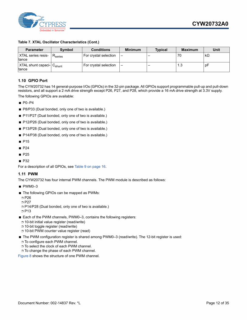
Table 7. XTAL Oscillator Characteristics
Parameter Symbol Conditions Minimum Typical Maximum Unit
Output frequency Foscout – – 32.768 – kHz
Frequency tolerance
– Crystal dependent – 100 – ppm
Start-up time Tstartup – – – 500 ms
XTAL drive level Pdrv For crystal selection 0.5 – – μW
C2
C1
R1 32.768 kHzXTAL
Document Number: 002-14837 Rev. *L Page 12 of 35
CYW20732A0
1.10 GPIO Port
The CYW20732 has 14 general-purpose I/Os (GPIOs) in the 32-pin package. All GPIOs support programmable pull-up and pull-down resistors, and all support a 2 mA drive strength except P26, P27, and P28, which provide a 16 mA drive strength at 3.3V supply.
The following GPIOs are available:
P0–P4
P8/P33 (Dual bonded, only one of two is available.)
P11/P27 (Dual bonded, only one of two is available.)
P12/P26 (Dual bonded, only one of two is available.)
P13/P28 (Dual bonded, only one of two is available.)
P14/P38 (Dual bonded, only one of two is available.)
P15
P24
P25
P32
For a description of all GPIOs, see Table 9 on page 16.
1.11 PWM
The CYW20732 has four internal PWM channels. The PWM module is described as follows:
PWM0–3
The following GPIOs can be mapped as PWMs: P26 P27 P14/P28 (Dual bonded, only one of two is available.) P13
Each of the PWM channels, PWM0–3, contains the following registers: 10-bit initial value register (read/write) 10-bit toggle register (read/write) 10-bit PWM counter value register (read)
The PWM configuration register is shared among PWM0–3 (read/write). The 12-bit register is used: To configure each PWM channel. To select the clock of each PWM channel. To change the phase of each PWM channel.
Figure 8 shows the structure of one PWM channel.
XTAL series resis-tance
Rseries For crystal selection – – 70 kΩ
XTAL shunt capaci-tance
Cshunt For crystal selection – – 1.3 pF
Table 7. XTAL Oscillator Characteristics (Cont.)
Parameter Symbol Conditions Minimum Typical Maximum Unit

Document Number: 002-14837 Rev. *L Page 13 of 35
CYW20732A0
Figure 8. PWM Channel Block Diagram
1.12 Power Management Unit
The power management unit (PMU) provides power management features that can be invoked by software through power management registers or packet-handling in the baseband core.
1.12.1 RF Power Management
The BBC generates power-down control signals for the transmit path, receive path, PLL, and power amplifier to the 2.4 GHz trans-ceiver, which then processes the power-down functions accordingly.
1.12.2 Host Controller Power Management
Power is automatically managed by the firmware based on input device activity. As a power-saving task, the firmware controls the disabling of the on-chip regulator when in deep sleep mode.
pwm_cfg_adr register pwm#_init_val_adr register pwm#_togg_val_adr register
pwm#_cntr_adr
enable
cntr value is CM3 readable
clk_sel
o_flip
10'H000
10'H3FF
10
10 10
Example: PWM cntr w/ pwm#_init_val = 0 (dashed line)PWM cntr w/ pwm#_init_val = x (solid line)
10'Hx
pwm_out
pwm_togg_val_adr
pwm_out

Document Number: 002-14837 Rev. *L Page 14 of 35
CYW20732A0
1.12.3 BBC Power Management
There are several low-power operations for the BBC:
Physical layer packet handling turns RF on and off dynamically within packet TX and RX.
Bluetooth-specified low-power connection mode. While in these low-power connection modes, the CYW20732 runs on the low power oscillator (LPO) and wakes up after a predefined time period.
The CYW20732 automatically adjusts its power dissipation based on user activity. The following power modes are supported:
Active mode
Idle mode
Sleep mode
HIDOFF (Deep Sleep) mode
The CYW20732 transitions to the next lower state after a programmable period of user inactivity. Busy mode is immediately entered when user activity resumes.
In HIDOFF (Deep Sleep) mode, the CYW20732 baseband and core are powered off by disabling power to LDOOUT. The VDDO domain remains powered up and will turn the remainder of the chip on when it detects user events. This mode minimizes chip power consumption and is intended for long periods of inactivity.

Document Number: 002-14837 Rev. *L Page 15 of 35
CYW20732A0
2. Pin Assignments
2.1 Pin Descriptions
Table 8. Pin Descriptions
Pin Number Pin Name I/O Power Domain Description
Radio I/O
6 RF I/O VDD_RF RF antenna port
RF Power Supplies
4 VDDIF I VDD_RF IFPLL power supply
5 VDDFE I VDD_RF RF front-end supply
7 VDDVCO I VDD_RF VCO, LOGEN supply
8 VDDPLL I VDD_RF RFPLL and crystal oscillator supply
Power Supplies
11 VDDC I VDDC Baseband core supply
28 VDDO I VDDO I/O pad and core supply
14 VDDM I VDDM I/O pad supply
Clock Generator and Crystal Interface
9 XTALI I VDD_RF Crystal oscillator input. See page 10 for options.
10 XTALO O VDD_RF Crystal oscillator output.
1 XTALI32K I VDDO LPO input is used. Alternative Function:
P11
P27
32 XTALO32K O VDDO LPO output. Alternative Function:
P12
P26
Core
18 RESET_N I/O PU VDDO Active-low system reset with open-drain output & internal pull-up resistor
17 TMC I VDDO Test mode controlHigh: test modeConnect to GND if not used.
UART
12 UART_RXD I VDDM UART serial input – Serial data input for the HCI UART interface. Leave unconnected if not used. Alternative function:
GPIO3
13 UART_TXD O, PU VDDM UART serial output – Serial data output for the HCI UART interface. Leave unconnected if not used.Alternative Function:
GPIO2
BSC

Document Number: 002-14837 Rev. *L Page 16 of 35
CYW20732A0
15 SDA I/O, PU VDDM Data signal for an external I2C device.Alternative function:
SPI_1: MOSI (master only)
GPIO0
CTS
16 SCL I/O, PU VDDM Clock signal for an external I2C device.Alternative function:
SPI_1: SPI_CLK (master only)
GPIO1
RTS
LDO Regulator Power Supplies
2 LDOIN I N/A Battery input supply for the LDO
3 LDOOUT O N/A LDO output
Table 9. GPIO Pin Descriptionsa
Pin Number Pin Name Default Di-rection
After POR State
Power Do-main Alternate Function Description
19 P0 Input Input floating
VDDO GPIO: P0
A/D converter input
Peripheral UART: puart_tx
SPI_2: MOSI (master and slave)
IR_RX
60Hz_main
Not available during TMC=1
20 P1 Input Input floating
VDDO GPIO: P1
A/D converter input
Peripheral UART: puart_rts
SPI_2: MISO (master and slave)
IR_TX
21 P3 Input Input floating
VDDO GPIO: P3
Peripheral UART: puart_cts
SPI_2: SPI_CLK (master and slave)
22 P2 Input Input floating
VDDO GPIO: P2
Peripheral UART: puart_rx
SPI_2: SPI_CS (slave only)
SPI_2: SPI_MOSI (master only)
Table 8. Pin Descriptions (Cont.)
Pin Number Pin Name I/O Power Domain Description

Document Number: 002-14837 Rev. *L Page 17 of 35
CYW20732A0
23 P4 Input Input floating
VDDO GPIO: P4
Peripheral UART: puart_rx
SPI_2: MOSI (master and slave)
IR_TX
24 P8 Input Input floating
VDDO GPIO: P8
A/D converter input
External T/R switch control: ~tx_pd
P33 Input Input floating
VDDO GPIO: P33
A/D converter input
SPI_2: MOSI (slave only)
Auxiliary clock output: ACLK1
Peripheral UART: puart_rx
1 P11 Input Input floating
VDDO GPIO: P11
A/D converter input
XTALI32K
P27PWM1
Input Input floating
VDDO GPIO: P27
SPI_2: MOSI (master and slave)
Current: 16 mA
32 P12 Input Input floating
VDDO GPIO: P12
A/D converter input
XTALO32K
P26PWM0
Input Input floating
VDDO GPIO: P26
SPI_2: SPI_CS (slave only)
SPI_1: MISO (master only)
Current: 16 mA
29 P13PWM3
Input Input floating
VDDO GPIO: P13
A/D converter input
P28PWM2
Input Input floating
VDDO GPIO: P28
A/D converter input
LED1
IR_TX
Current: 16 mA
Table 9. GPIO Pin Descriptionsa (Cont.)
Pin Number Pin Name Default Di-rection
After POR State
Power Do-main Alternate Function Description

Document Number: 002-14837 Rev. *L Page 18 of 35
CYW20732A0
30 P14PWM2
Input Input floating
VDDO GPIO: P14
A/D converter input
P38 Input Input floating
VDDO GPIO: P38
A/D converter input
SPI_2: MOSI (master and slave)
IR_TX
31 P15 Input Input floating
VDDO GPIO: P15
A/D converter input
IR_RX
60 Hz_main
27 P24 Input Input floating
VDDO GPIO: P24
SPI_2: SPI_CLK (master and slave)
SPI_1: MISO (master only)
Peripheral UART: puart_tx
26 P25 Input Input floating
VDDO GPIO: P25
SPI_2: MISO (master and slave)
Peripheral UART: puart_rx
25 P32 Input Input floating
VDDO GPIO: P32
A/D converter input
SPI_2: SPI_CS (slave only)
SPI_1: MISO (master only)
Auxiliary clock output: ACLK0
Peripheral UART: puart_tx
a. During power-on reset, all inputs are disabled.
Table 9. GPIO Pin Descriptionsa (Cont.)
Pin Number Pin Name Default Di-rection
After POR State
Power Do-main Alternate Function Description

Document Number: 002-14837 Rev. *L Page 19 of 35
CYW20732A0
2.2 Ball Maps
Figure 9. 32-pin QFN Ball Map
1
2
3
4
5
6
7
8 9 10 11 12 13 14 15 16
17
18
19
20
21
22
23
24
25 26 27 28 29 30 31 32
P11/P27/XIN32
LDO_IN
LDO_OUT
VDDIF
VDDFE
RF
VDDVCO
VDDPLL
XTAL
I
XTAL
O
VDDC
UAR
T_RX
D
UAR
T_TX
D
VDDM
SDA
SCL
TMC
RST_N
P0
P1
P3
P2
P4
P8/P33
P32
P25
P24
VDDO
P13/
P28
P14/
P38 P15
P12/
P26/
XO32

Document Number: 002-14837 Rev. *L Page 20 of 35
CYW20732A0
3. Specifications
3.1 Electrical Characteristics
Table 10 shows the maximum electrical rating for voltages referenced to VDD pin.
Table 11 shows the power supply characteristics for the range TJ = 0 to 125°C.
Table 10. Maximum Electrical Rating
Rating Symbol Value Unit
DC supply voltage for RF domain – 1.4 V
DC supply voltage for core domain – 1.4 V
DC supply voltage for VDDM domain (UART/I2C) – 3.8 V
DC supply voltage for VDDO domain – 3.8 V
DC supply voltage for VR3V – 3.8 V
DC supply voltage for VDDFE – 1.4 V
Voltage on input or output pin – VSS – 0.3 to VDD + 0.3 V
Operating ambient temperature range Topr –30 to +85 °C
Storage temperature range Tstg –40 to +125 °C
Table 11. Power Supply
Parameter Minimuma
a. Overall performance degrades beyond minimum and maximum supply voltages.
Typical Maximuma Unit
DC supply voltage for RF 1.14 1.2 1.26 V
DC supply voltage for Core 1.14 1.2 1.26 V
DC supply voltage for VDDM (UART/I2C) 1.62 – 3.63 V
DC supply voltage for VDDO 1.62 – 3.63 V
DC supply voltage for LDOIN 1.425 – 3.63 V
DC supply voltage for VDDFE 1.14 1.2b
b. 1.2V for Class 2 output with internal VREG.
1.26 V

Document Number: 002-14837 Rev. *L Page 21 of 35
CYW20732A0
Table 12 shows the digital level characteristics for (VSS = 0V).
Table 13 shows the specifications for the ADC characteristics.
Table 14 shows the specifications for the digital voltage levels.
Table 12. LDO Regulator Electrical Specifications
Parameter Conditions Min. Typ. Max. Unit
Input voltage range – 1.425 – 3.63 V
Default output voltage – – 1.2 – V
Output voltage Range 0.8 – 1.4 V
Step size – 40 or 80 – mV
Accuracy at any step –5 – +5 %
Load current – – – 30 mA
Line regulation Vin from 1.425 to 3.63V, Iload = 30 mA –0.2 – 0.2 %VO/V
Load regulation Iload from 1 µA to 30 mA, Vin = 3.3V, Bonding R = 0.3Ω
– 0.1 0.2 %VO/mA
Quiescent current No load @Vin = 3.3V*Current limit enabled
– 6 – µA
Power-down current Vin = 3.3V, worst@70°C – 5 200 nA
Table 13. ADC Specifications
Parameter Symbol Conditions Min. Typ. Max. Unit
Number of Input channels – – – 9 – –
Channel switching rate fch – – – 133.33 kch/s
Input signal range Vinp – 0 – 3.63 V
Reference settling time – Changing refsel 7.5 – – s
Input resistance Rinp Effective, single ended – 500 – k
Input capacitance Cinp – – – 5 pF
Conversion rate fC – 5.859 – 187 kHz
Conversion time TC – 5.35 – 170.7 s
Resolution R – – 16 – bits
Effective number of bits – In specified performance range – See Table 2 on page 6
– –
Absolute voltage measurement error
– Using on-chip ADC firmware driver – ±2 – %
Current I Iavdd1p2 + Iavdd3p3 – – 1 mA
Power P – – 1.5 – mW
Leakage current Ileakage T = 25°C – – 100 nA
Power-up time Tpowerup – – – 200 µs
Integral nonlinearity3 INL In guaranteed performance range –1 – 1 LSBa
a. LSBs are expressed at the 10-bit level.
Differential nonlinearitya DNL In guaranteed performance range –1 – 1 LSBa

Document Number: 002-14837 Rev. *L Page 22 of 35
CYW20732A0
Table 15 shows the specifications for current consumption.
Table 14. Digital Levelsa
a. This table is also applicable to VDDMEM domain.
Characteristics Symbol Min Typ Max Unit
Input low voltage VIL – – 0.4 V
Input high voltage VIH 0.75 × VDDO – – V
Input low voltage (VDDO = 1.62V) VIL – – 0.4 V
Input high voltage (VDDO = 1.62V) VIH 1.2 – – V
Output low voltageb
b. At the specified drive current for the pad.
VOL – – 0.4 V
Output high voltageb VOH VDDO – 0.4 – – V
Input capacitance (VDDMEM domain) CIN – 0.12 – pF
Table 15. Current Consumption a
a. Currents measured between power terminals (Vdd) using 90% efficient DC-DC converter at 3V.
Operational Mode Conditions Min Typ Max Unit
Receive Receiver and baseband are both operating, 100% ON. – 9.8 – mA
Transmit Transmitter and baseband are both operating, 100% ON. – 9.1 – mA
Sleep Internal LPO is in use. – 12.0 – μA
– – 0.65 –

Document Number: 002-14837 Rev. *L Page 23 of 35
CYW20732A0
3.2 RF Specifications
Table 16. Receiver RF Specifications
Parameter Mode and Conditions Min Typ Max Unit
Receiver Sectiona
a.30.8% PER.
Frequency range – 2402 – 2480 MHz
RX sensitivity (standard) 0.1%BER, 1Mbps, dirty transmitter OFF – –93 – dBm
RX sensitivity (low current) – –90 – dBm
Input IP3 – –16 – – dBm
Maximum input – –10 – – dBm
Interference Performancea,b
b.Desired signal is 3 dB above the reference sensitivity level (defined as –70 dBm).
C/I cochannel 0.1%BER – – 21 dB
C/I 1 MHz adjacent channel 0.1%BER – – 15 dB
C/I 2 MHz adjacent channel 0.1%BER – – –17 dB
C/I 3 MHz adjacent channel 0.1%BER – – –27 dB
C/I image channel 0.1%BER – – –9.0 dB
C/I 1 MHz adjacent to image channel 0.1%BER – – –15 dB
Out-of-Band Blocking Performance (CW)a,b
30 MHz to 2000 MHz 0.1%BERc
c. Measurement resolution is 10 MHz.
– –30.0 – dBm
2003 MHz to 2399 MHz 0.1%BERd
d. Measurement resolution is 3 MHz.
– –35 – dBm
2484 MHz to 2997 MHz 0.1%BERd – –35 – dBm
3000 MHz to 12.75 GHz 0.1%BERe
e. Measurement resolution is 25 MHz.
– –30.0 – dBm
Spurious Emissions
30 MHz to 1 GHz – – – –57.0 dBm
1 GHz to 12.75 GHz – – – –55.0 dBm
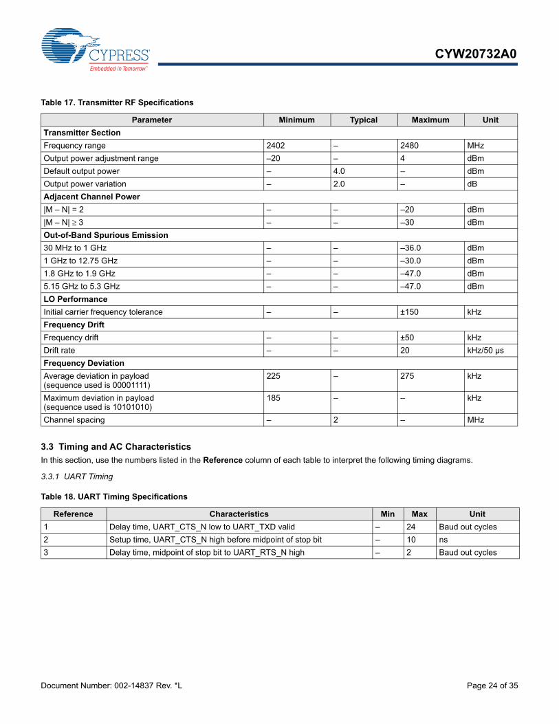
Document Number: 002-14837 Rev. *L Page 24 of 35
CYW20732A0
3.3 Timing and AC Characteristics
In this section, use the numbers listed in the Reference column of each table to interpret the following timing diagrams.
3.3.1 UART Timing
Table 17. Transmitter RF Specifications
Parameter Minimum Typical Maximum Unit
Transmitter Section
Frequency range 2402 – 2480 MHz
Output power adjustment range –20 – 4 dBm
Default output power – 4.0 – dBm
Output power variation – 2.0 – dB
Adjacent Channel Power
|M – N| = 2 – – –20 dBm
|M – N| 3 – – –30 dBm
Out-of-Band Spurious Emission
30 MHz to 1 GHz – – –36.0 dBm
1 GHz to 12.75 GHz – – –30.0 dBm
1.8 GHz to 1.9 GHz – – –47.0 dBm
5.15 GHz to 5.3 GHz – – –47.0 dBm
LO Performance
Initial carrier frequency tolerance – – ±150 kHz
Frequency Drift
Frequency drift – – ±50 kHz
Drift rate – – 20 kHz/50 µs
Frequency Deviation
Average deviation in payload(sequence used is 00001111)
225 – 275 kHz
Maximum deviation in payload(sequence used is 10101010)
185 – – kHz
Channel spacing – 2 – MHz
Table 18. UART Timing Specifications
Reference Characteristics Min Max Unit
1 Delay time, UART_CTS_N low to UART_TXD valid – 24 Baud out cycles
2 Setup time, UART_CTS_N high before midpoint of stop bit – 10 ns
3 Delay time, midpoint of stop bit to UART_RTS_N high – 2 Baud out cycles

Document Number: 002-14837 Rev. *L Page 25 of 35
CYW20732A0
Figure 10. UART Timing
3.3.2 SPI Timing
The SPI interface supports clock speeds up to 12 MHz with VDDIO ≥ 2.2V. The supported clock speed is 6 MHz when 2.2V > VDDIO ≥ 1.62V.
Figure 11 and Figure 12 on page 26 show the timing requirements when operating in SPI Mode 0 and 2, and SPI Mode 1 and 3, respectively.
Table 19. SPI Interface Timing Specifications
Reference Characteristics Min Typ Max
1 Time from CSN asserted to first clock edge 1 SCK 100 ∞
2 Master setup time – ½ SCK –
3 Master hold time ½ SCK – –
4 Slave setup time – ½ SCK –
5 Slave hold time ½ SCK – –
6 Time from last clock edge to CSN deasserted 1 SCK 10 SCK 100

Document Number: 002-14837 Rev. *L Page 26 of 35
CYW20732A0
Figure 11. SPI Timing – Mode 0 and 2
Figure 12. SPI Timing – Mode 1 and 3
3.3.3 BSC Interface Timing
Table 20. BSC Interface Timing Specifications
Reference Characteristics Min Max Unit
1 Clock frequency – 100 kHz
400
800
1000
2 START condition setup time 650 – ns
3 START condition hold time 280 – ns
4 Clock low time 650 – ns
5 Clock high time 280 – ns
6 Data input hold timea 0 – ns
3
SPI_CSN
SPI_CLK(Mode 0)
SPI_MOSI ‐ First Bit
SPI_MISO Not Driven First Bit
Second Bit
Second Bit
Last bit
Last bit
1
2
6
SPI_CLK(Mode 2)
Not Driven
‐
54
3
SPI_CSN
SPI_CLK(Mode 1)
SPI_MOSI ‐ Invalid bit
SPI_MISO Not Driven Invalid bit
First bit
First bit
Last bit
Last bit
1
2
6
‐
Not Driven
SPI_CLK(Mode 3)
54

Document Number: 002-14837 Rev. *L Page 27 of 35
CYW20732A0
Figure 13. BSC Interface Timing Diagram
7 Data input setup time 100 – ns
8 STOP condition setup time 280 – ns
9 Output valid from clock – 400 ns
10 Bus free timeb 650 – ns
a. As a transmitter, 300 ns of delay is provided to bridge the undefined region of the falling edge of SCL to avoid unintended generation of START or STOP conditions.
b. Time that the cbus must be free before a new transaction can start.
Table 20. BSC Interface Timing Specifications
Reference Characteristics Min Max Unit

Document Number: 002-14837 Rev. *L Page 28 of 35
CYW20732A0
3.4 ESD Test Models
ESD can have serious detrimental effects on all semiconductor ICs and the system that contains them. Standards are developed to enhance the quality and reliability of ICs by ensuring all devices employed have undergone proper ESD design and testing, thereby minimizing the detrimental effects of ESD. Three major test methods are widely used in the industry today to describe uniform methods for assessing ESD immunity at Component level, Human Body Model (HBM), Machine Model (MM), and Charged Device Model (CDM). The following standards were used to test this device:
3.4.1 Human-Body Model (HBM) – ANSI/ESDA/JEDEC JS-001-2012
The HBM has been developed to simulate the action of a human body discharging an accumulated static charge through a device to ground, and employs a series RC network consisting of a 100 pF capacitor and a 1500Ω (Ohm) resistor. Both positive and negative polarities are used for this test. Although, a 100 ms delay is allowable per specification, the minimum delay used for testing was set to 300 ms between each pulse.
3.4.2 Machine Model (MM) – JEDEC JESD22-A115C
The MM has been developed to simulate the rapid discharge from a charged conductive object, such as a metallic tool or fixture. The most common application would be rapid discharge from charged board assembly or the charged cables of automated testers. This model consists of a 200 pF capacitor discharged directly into a component with no series resistor (0Ω). One positive and one negative polarity pulses are applied. The minimum delay between pulses is 500 ms.
3.4.3 Charged-Device Model (CDM) - JEDEC JESD22-C101E
CDM simulates charging/discharging events that occur in production equipment and processes. The potential for a CDM ESD events occurs when there is metal-to-metal contact in manufacturing. CDM addresses the possibility that a charge may reside on the lead frame or package (e.g., from shipping) and discharge through a pin that subsequently is grounded, causing damage to sensitive devices in the path. Discharge current is limited only by the parasitic impedance and capacitance of the device. CDM testing consists of charging package to a specified voltage, then discharging the voltage through relevant package leads. One positive and one negative polarity pulse is applied. The minimum delay between pulses is 200 ms.
3.4.4 Results Summary
ESD Test Voltage Level Results:
HBM +/– 2KV PASS
CDM +/– 500V PASS
MM +/– 150V PASS

Document Number: 002-14837 Rev. *L Page 29 of 35
CYW20732A0
4. Mechanical Information
Figure 14. 32-Pin 5x5 mm QFN Package

Document Number: 002-14837 Rev. *L Page 30 of 35
CYW20732A0
Table 21 provides dimensions and additional details on the 32-pin 5x5 mm QFN package.
4.0.1 Tape Reel and Packaging Specifications
The top left corner of the CYW20732 package is situated near the sprocket holes, as shown in Figure 15.
Figure 15. Pin 1 Orientation
Table 21. 32-pin 5x5 mm QFN Package Dimensions (Footprint: 0.80)
S/N SYM Dimension Comments/Specifications
1 A 0.900 ±0.100 Overall Height
General tolerance: Distance: ±0.100
Angle:
2 A1 0.020 ±TBD Standoff
Matte finish on package body surface, except ejection and pin 1 marking.
Ra 0.3 ~ 1.2 μm
3 D 5.000 ±0.100 Package Length
Frame base metal thickness 0.203 base
4 E 5.000 ±0.100 Package Width
All molded body sharp corner radii; unless otherwise specified. R0.200 (maximum)
5 L 0.400 ±0.075 Foot Length
Drawing does not include plastic or metal protrusion of cutting burr.
6 T 0.203 Ref. Frame Thickness
Compliant to JEDEC standard: MO-220.
7 b 0.250 ±0.050 Lead Width
8 e 0.500 Base Lead Pitch
Table 22. CYW20732 5 × 5 × 1 mm QFN, 32-Pin Tape Reel Specifications
Parameter Value
Quantity per reel 2500 pieces
Reel diameter 13 inches
Hub diameter 7 inches
Tape width 12 mm
Tape pitch 8 mm
Pin 1: Top left corner of package toward sprocket holes

Document Number: 002-14837 Rev. *L Page 31 of 35
CYW20732A0
5. Ordering Information
Table 23. Ordering Information
Part Number Package Ambient Operating Temperature
CYW20732A0KML2G 32-pin QFN –30°C to +85°C

Document Number: 002-14837 Rev. *L Page 32 of 35
CYW20732A0
A. Appendix: Acronyms and Abbreviations
The following list of acronyms and abbreviations may appear in this document.
Term Description
ADC analog-to-digital converter
AFH adaptive frequency hopping
AHB advanced high-performance bus
APB advanced peripheral bus
APU audio processing unit
ARM7TDMI-S Acorn RISC Machine 7 Thumb instruction, Debugger, Multiplier, Ice, Synthesizable
CSC Cypress Serial Control
BTC Bluetooth controller
COEX coexistence
DFU device firmware update
DMA direct memory access
EBI external bus interface
HCI Host Control Interface
HV high voltage
IDC initial digital calibration
IF intermediate frequency
IRQ interrupt request
JTAG Joint Test Action Group
LCU link control unit
LDO low drop-out
LHL lean high land
LPO low power oscillator
LV LogicVision
MIA multiple interface agent
PCM pulse code modulation
PLL phase locked loop
PMU power management unit
POR power-on reset
PWM pulse width modulation
QD quadrature decoder
RAM random access memory
RF radio frequency
ROM read-only memory
RX/TX receive, transmit
SPI serial peripheral interface
SW software
UART universal asynchronous receiver/transmitter
UPI µ-processor interface
WD watchdog

Document Number: 002-14837 Rev. *L Page 33 of 35
CYW20732A0
Document History
Document Title: CYW20732A0 Single-Chip Bluetooth Low-Energy Only SoCDocument Number: 002-14837
Revision ECN Orig. of Change Submission Date Description of Change
** - - 6/27/201120732-DS100-R: Initial release
*A - - 2/24/2012
20732-DS101-R:
Updated:• Document title changed.• “Bluetooth Low Energy Features” on page 1.• Table 8: “GPIO Pin Descriptions,” on page 16.• Table 15: “Receiver RF Specifications,” on page 23.• Table 16: “Transmitter RF Specifications,” on page 24.• “SPI Timing” on page 25.
*B - - 9/17/2012
20732-DS102-R:
Updated:• ‘Preliminary Data Sheet’ to ‘Data Sheet’.• ‘HIDOFF mode’ to ‘HIDOFF (Deep Sleep) mode’.
*C - -7/10/2013
20732-DS103-R:
Updated:• “Bluetooth Low Energy Features” on page 1.• “Microprocessor Unit” on page 07.• Table 9: “Maximum Electrical Rating,” on page 20• Table 21: “Ordering Information,” on page 31.
*D - - 9/17/2013
20732-DS104-R:
Updated:• Table 14: “Current Consumption,” on page 22: RX/Tx maximumcurrent values.
*E - - 10/03/2013
20732-DS105-R:
Updated:• Table 14: “Current Consumption,” on page 22.
*F - 12/12/2013
20732-DS106-R:
Updated:• Table 16: “Transmitter RF Specifications,” on page 24
*G - - 3/26/2014
20732-DS107-R: Updated:• Figure 14: “32-Pin 5x5 mm QFN Package,” on page 30Added:• Table 20: “32-pin 5x5 mm QFN Package Dimensions (Footprint:0.80),” on page 30
*H - - 06/05/2014
20732-DS108-R: Updated:• “UART Interface” on page 10.
*I - - 11/24/2014
20732-DS109-R: Updated:• Table 5: “Reference Crystal Electrical Specifications,” on page10
*J - - 04/21/2015
20732-DS110-R:
Updated:
• Table15:“Receiver RF Specifications,” on page23
Document Number: 002-14837 Rev. *L Page 34 of 35
CYW20732A0
*K - - 02/16/2016
20732-DS111-R:
Added:
• “ESD Test Models” on page 27
*L 5448744 UTSV 11/02/2016 Migrated to Cypress template.
Document Title: CYW20732A0 Single-Chip Bluetooth Low-Energy Only SoCDocument Number: 002-14837

Document Number: 002-14837 Rev. *L Revised November 2, 2016 Page 35 of 35
CYW20732A0
© Cypress Semiconductor Corporation, 2011-2016. This document is the property of Cypress Semiconductor Corporation and its subsidiaries, including Spansion LLC (“Cypress”). This document,including any software or firmware included or referenced in this document (“Software”), is owned by Cypress under the intellectual property laws and treaties of the United States and other countriesworldwide. Cypress reserves all rights under such laws and treaties and does not, except as specifically stated in this paragraph, grant any license under its patents, copyrights, trademarks, or otherintellectual property rights. If the Software is not accompanied by a license agreement and you do not otherwise have a written agreement with Cypress governing the use of the Software, then Cypresshereby grants you a personal, non-exclusive, nontransferable license (without the right to sublicense) (1) under its copyright rights in the Software (a) for Software provided in source code form, tomodify and reproduce the Software solely for use with Cypress hardware products, only internally within your organization, and (b) to distribute the Software in binary code form externally to end users(either directly or indirectly through resellers and distributors), solely for use on Cypress hardware product units, and (2) under those claims of Cypress's patents that are infringed by the Software (asprovided by Cypress, unmodified) to make, use, distribute, and import the Software solely for use with Cypress hardware products. Any other use, reproduction, modification, translation, or compilationof the Software is prohibited.
TO THE EXTENT PERMITTED BY APPLICABLE LAW, CYPRESS MAKES NO WARRANTY OF ANY KIND, EXPRESS OR IMPLIED, WITH REGARD TO THIS DOCUMENT OR ANY SOFTWAREOR ACCOMPANYING HARDWARE, INCLUDING, BUT NOT LIMITED TO, THE IMPLIED WARRANTIES OF MERCHANTABILITY AND FITNESS FOR A PARTICULAR PURPOSE. To the extentpermitted by applicable law, Cypress reserves the right to make changes to this document without further notice. Cypress does not assume any liability arising out of the application or use of anyproduct or circuit described in this document. Any information provided in this document, including any sample design information or programming code, is provided only for reference purposes. It isthe responsibility of the user of this document to properly design, program, and test the functionality and safety of any application made of this information and any resulting product. Cypress productsare not designed, intended, or authorized for use as critical components in systems designed or intended for the operation of weapons, weapons systems, nuclear installations, life-support devices orsystems, other medical devices or systems (including resuscitation equipment and surgical implants), pollution control or hazardous substances management, or other uses where the failure of thedevice or system could cause personal injury, death, or property damage (“Unintended Uses”). A critical component is any component of a device or system whose failure to perform can be reasonablyexpected to cause the failure of the device or system, or to affect its safety or effectiveness. Cypress is not liable, in whole or in part, and you shall and hereby do release Cypress from any claim,damage, or other liability arising from or related to all Unintended Uses of Cypress products. You shall indemnify and hold Cypress harmless from and against all claims, costs, damages, and otherliabilities, including claims for personal injury or death, arising from or related to any Unintended Uses of Cypress products.
Cypress, the Cypress logo, Spansion, the Spansion logo, and combinations thereof, WICED, PSoC, CapSense, EZ-USB, F-RAM, and Traveo are trademarks or registered trademarks of Cypress inthe United States and other countries. For a more complete list of Cypress trademarks, visit cypress.com. Other names and brands may be claimed as property of their respective owners.
Sales, Solutions, and Legal Information
Worldwide Sales and Design Support
Cypress maintains a worldwide network of offices, solution centers, manufacturer’s representatives, and distributors. To find the office closest to you, visit us at Cypress Locations.
Products
ARM® Cortex® Microcontrollers cypress.com/arm
Automotive cypress.com/automotive
Clocks & Buffers cypress.com/clocks
Interface cypress.com/interface
Internet of Things cypress.com/iot
Lighting & Power Control cypress.com/powerpsoc
Memory cypress.com/memory
PSoC cypress.com/psoc
Touch Sensing cypress.com/touch
USB Controllers cypress.com/usb
Wireless/RF cypress.com/wireless
PSoC®Solutions
PSoC 1 | PSoC 3 | PSoC 4 | PSoC 5LP
Cypress Developer Community
Forums | WICED IoT Forums | Projects | Video | Blogs |Training | Components
Technical Support
cypress.com/support
35