Cyclone V SoC base board User’s Manual
38
Preliminary Cyclone V SoC base board users manual Cyclone V SoC base board User’s Manual Model Number: < Altc5bb5csxc6NES> v0.35 March 25, 2013 ALTIMA Corp.
Transcript of Cyclone V SoC base board User’s Manual

Preliminary
Cyclone V SoC base board user’s manual
Cyclone V SoC base board User’s Manual
Model Number: < Altc5bb5csxc6NES>
v0.35
March 25, 2013
ALTIMA Corp.

Preliminary
Cyclone V SoC base board user’s manual
Document Revision History
Revision Date Author Remarks 0.1 2012/12/19 T.Mizukawa Preliminary version 0.2 2013/01/25 K.Yoshimoto Add some details
0.2e 2013/01/25 T.Mizukawa Translate in English
0.3 2013/01/31 K.Yoshimoto 設計時の変更内容を反映
0.31 2013/02/05 K.Yoshimoto LCD インターフェース変更に伴う変更
0.32 2013/02/27 K.Yoshimoto Board Block差し替えJTAG Chain差し替え、JTAG Setting DIP Switch変更
0.33 2013/03/05 K.YoshimotoBoard top viewの図を変更 JTAG Setting DIPS Switchの SW4-3、SW4-4の説明を変更Components and Interfacesに I2Cの説明を追加
0.34 2013/03/22 T.Mizukawa Rename document title [Functional spec] user’s manual
0.35 2013/03/25 K.Yoshimoto Modify figure 1 QSPI Flash 128MB to 64MB Modify figure 5.

Preliminary
Cyclone V SoC base board user’s manual
IMPORTANT INFORMATION READ FIRST READ this user's manual before using this product.
KEEP the user's manual handy for future reference.
Do not attempt to use the product until you fully understand its mechanism.
This Product:
In this manual, this product points out the following product which ALTIMA Corp. manufactured.
Purpose of the Product:
This product is the Cyclone V SX SoC base board to support the development of a system that uses
the Cyclone V SX SoC of Altera Corporation. It provides support for system development in both
software and hardware.
For those who use this product:
This product can only be used by those who have carefully read the user's manual and know how to
use it. Use of this product requires the basic knowledge of electric circuits, logical circuits, and FPGAs.
All Rights Reserved:
This user's manual and product are copyrighted and all rights are reserved by ALTIMA Corp.
Improvement Policy:
ALTIMA Corp. pursues a policy of continuing improvement in design, performance, and safety of the
product. ALTIMA Corp. reserves the right to change, wholly or partially, the specifications, design,
user's manual, and other documentation at any time without notice.
Figures:
Some figures in this user's manual may show items different from your actual system.

Preliminary
Cyclone V SoC base board user’s manual
Contents
1. Overview ............................................................................................................................................ 1 1.1. Key Components ........................................................................................................................... 1 1.2. Block Diagram ............................................................................................................................... 2 1.3. Board Specification ....................................................................................................................... 2 2. Board Overview ................................................................................................................................. 3 2.1. Featured Device: Cyclone V SoC ................................................................................................. 6 2.1.1. I/O Resources ............................................................................................................................. 6 2.2. JTAG Configuration....................................................................................................................... 7 2.2.1. FPGA Configuration .................................................................................................................. 8 2.2.2. HPS Configuration ..................................................................................................................... 8 2.3. Status Elements........................................................................................................................... 10 2.4. Setup Elements ............................................................................................................................ 11 2.4.1. JTAG settings DIP switch ....................................................................................................... 11 2.4.2. HPS reset push button ............................................................................................................ 12 2.4.3. Program configuration push button ...................................................................................... 13 2.4.4. HPS settings Jumper switch .................................................................................................. 13 3. Clock Tree(Subject to change) ..................................................................................................... 14 4. General User Input/Output ............................................................................................................. 16 4.1. User-Defined Push Buttons ....................................................................................................... 16 4.2. User-Defined DIP Switch ............................................................................................................ 16 4.3. User-Defined LEDs ...................................................................................................................... 17 4.4. Character LCD ............................................................................................................................. 17 4.5. Debug Header .............................................................................................................................. 18 5. Components and Interfaces ........................................................................................................... 19 5.1. 10/100/1000 Ethernet ................................................................................................................... 19 5.2. HSMC ............................................................................................................................................ 21 5.3. USB2.0 OTG ................................................................................................................................. 26 5.4. UART ............................................................................................................................................. 27 5.5. SD .................................................................................................................................................. 27 5.6. I2C ................................................................................................................................................. 28 6. Memory ............................................................................................................................................. 29 6.1. DDR3 SDRAM ............................................................................................................................... 29 6.2. QSPI FlashROM ........................................................................................................................... 32 7. Power Supply .................................................................................................................................. 33 7.1. Power Distribution System......................................................................................................... 33

Preliminary 1 / 38
Cyclone V SoC base board user’s manual
1. Overview This document describes the hardware features of the Altera Cyclone® V SoC Base Board. Cyclone® V
SX SoC include the Hard Processor System (HPS) with integrated ARM® Cortex™-A9MPCore processor.
For more information on the Cyclone V, refer to the following documents:
■ Cyclone V device family, refer to the Cyclone V Device Handbook.
1.1. Key Components Cyclone V SoC Base Board Following key components are implemented on Cyclone V SoC base
board.
Key components are listed in Table 1. Table 1 Key Components
Supplyer Function Name Part number
CPU Altera SoC with FPGA 5CSXFC6C6U23C8NES
Configuration ROM Altera Configuration device EPCQ256SI16N
CPLD Altera On-board USB Blaster II EPM570GF100C5N
ROM Micron 512Mb QSPI NOR FlashROM N25Q512A13GSF40G
Microchip EEPROM 24LC32A
RAM Micron DDR3-SDRAM MT41J64M16JT-125
Ethernet Micrel Gigabit Ethernet PHY KSZ9021RN
USB SMSC(Microchip) OTG USB PHY USB3300-EZK
Cypress USB PHY for USB Blaster II CY7C68013A-56BAXC
Real Time Clock MAXIM I2C Real time clock DS1339C-33#
UART Silicon Labs USB to UART bridge CP2103GM
Connector TE Connectivity Mictor for HPS 2-5767004-2
Samtec HSMC ASP-122953-01

Preliminary 2 / 38
Cyclone V SoC base board user’s manual
1.2. Block Diagram Figure 1 shows a block diagram of the Cyclone V SoC base board.
Figure 1 Cylcone V SoC base board Block Diagram
1.3. Board Specification
PCB Size Height Width
100mm 167mm
PCB thickness 1.6mm
Layer number 8 Layers

Preliminary 3 / 38
Cyclone V SoC base board user’s manual
2. Board Overview This section provides an overview of the Cyclone V SX SoC base board Figure 2-1 shows an top view
of the board.
Figure 2-1 Board top view
Table 2–1 describes the components and lists their corresponding board references.
Table 2–1. Board Components
Board Reference Type Description
Featured Devices
U1 SoC Cyclone V SX SoC, 5CSXFC6C6U23C8NES,
672-pin UBGA.
U31 CPLD MAX II CPLD, EPM570GF100C5N, 100-pin FBGA
Configuration, Status, and Setup Elements
J2 JTAG 10pin header
Provides access to the JTAG chain and disables the
embedded USB-Blaster II when using an external
USB-Blaster cable.
Warm ResetPush Button
(SW6)MAXII CPLD
(U31)
Cold ResetPush Button
(SW5)
User DefinedDip SwitchFor HPS(SW14)
User DefinedPush Button
For HPS(SW7-SW10)
JTAG Master Select DIP
Switch(SW4)
JTAG 10pinHeader
(J2)
HSMC Port(J4)
Cyclone V SXSoC (U1)
MICTOR_38P Port (J1)
UART Port(J9)
Gigabit Ethernet Port (J9)
Micro SD Socket Port (J7)
DDR3 x32 memory
(U16, U17)
Character LCD Port (J8)
On Board USB Blaster II Port
(J11)
USB 2.0 OTG Port (J6)
User GPIO TH (GPIO057,58,59,
61)
JTAG Chain Setting
DIP Switch (U1)
Re-configurationPush Button
(SW3)
HPS Setting Jumper Switch
(J16-J20)
User DIP Switch For FPGA
(SW15)
User Push Button For FPGA
(SW11-SW13)
Power Switch(SW16)
DC Input Jack(J14)
User LEDs(LED3-LED6)
Power MonitorPort (J15)

Preliminary 4 / 38
Cyclone V SoC base board user’s manual
SW1 JTAG chain control DIP Switch Remove or include devices in the active JTAG chain.
SW4 JTAG master select DIP Switch Select master I/F of JTAG chain, and master I/F for HPS.
J11 USB type-B connector
USB interface for FPGA programming and debugging
thorough the embedded USB Blaster II JTAG via a type-B
cable.
J16, J17, J18, J19,
J20 HPS setting Jumper switch Selects for the HPS boot source, and the clock mode.
SW3 Re-configuration push button FPGA reconfigured by the configuration ROM (EPCQ) when
pushed SW3.
SW5 Cold reset push button Cold reset: HPS and Ethernet are reset when pushed SW5.
SW6 Warm reset push button Warm reset: Only HPS is reset when pushed SW6.
LED1 Configuration done LED Illuminates when the FPGA is configured.
LED2 Cold reset LED Illuminates when the HPS is Cold reset.
LED7 UART Transmit LED Blink when there is UART data to transmit.
LED8 UART Receive LED Blink when there is data on the UART receive buffer.
LED14 Ethernet LINK LED Illuminates when the Ethernet linked.
LED15 Ethernet ACT LED Illuminates when the Ethernet activity.
Clock Circuitry
U6 100-MHz oscillator 100.000-MHz crystal oscillator for the GXB reference clock.
X1 50-MHz oscillator 50.000-MHz crystal oscillator for general purpose logic.
X2 25-MHz oscillator 25.000-MHz crystal oscillator for the HPS primary and
secondary clock.
X3 100-MHz oscillator 100.000-MHz crystal oscillator for general purpose logic.
X4 125-MHz oscillator 125.000-MHz crystal oscillator for general purpose logic.
General User Input/Output
LED3, LED4, LED5,
LED6 User LEDs Four user LEDs. Illuminates when driven low.
SW7, SW8, SW9,
SW10 User push button for HPS
Four user push buttons. Connected to the GPIO on the
HPS.
SW11, SW12,
SW13 User push button for FPGA Three user push buttons. Connected to the IO of the FPGA.
SW14 User DIP switch for HPS Four-bit DIP switch. Connected to the GPIO of the HPS.
SW15 User DIP switch for FPGA Four-bit DIP switch. Connected to the IO of the FPGA.
GPIO1, GPIO2,
GPIO3, GPIO4 User GPIO
Four GPIO through holes. Connected to the GPIO of the
HPS.
Memory Devices
U16, U17 DDR3-SDRAM 256MB DDR3-SDRAM (Two 128MB DDR3): Connected to
HPS with a 32-bit data bus.

Preliminary 5 / 38
Cyclone V SoC base board user’s manual
U21 QSPI-Flash memory 64MB QSPI NOR Flash memory: Connected to HPS.
HPS support serial, Dual, Quad I/O SPI protocols.
U7 FPGA configuration ROM
Serial or quad-serial FPGA configuration in devices that
support active serial ASx1 or ASx4 configuration schemes.
256-Mbit.
U19 EEPROM 32-kbit I2C Serial EEPROM. Connected to HPS
Communication Ports
J1 Mictor 38pin port The ARM DSTREM or third party debugger is able to
connect to Mictor 38pin port.
J4 HSMC port Provides four transceiver channels and 84CMOS or
17LVDS channels per the HSMC specification.
J5 Gigabit Ethernet port
RJ-45 connector which provides a 10/100/1000 Ethernet
connection via a Micrel KSZ9021RL and the HPS-based
Ethernet MAC in RGMII mode.
J6 USB 2.0 OTG port
USB mini-AB connector which provides a USB2.0 Hi-Speed
and OTG protocol via a SMSC USB3300 and the
HPS-based USB2.0 LINK in ULPI.
J7 Micro SD socket Micro SD socket which provides a Micro SD via the
HPS-based SD/SDIO/MMC flash controller.
J9 UART port USB mini-B connector which provides a USB-serial via a
Silicon Labs CP2103 and the HPS-based UART.
J11 On-Board USB Blaster II port
USB mini-B connector which provides the FPGA
configuration via a Cypress CY7C68013A and an Altera
MAXII CPLD.
Display Ports
J16 Character LCD Connector that interfaces to a provided 16character x2 line
LCD module along with two standoffs.
Power Supply
J14 DC input jack Accepts a 12-V DC power supply.
SW16 Power switch Switch to power on or off the board when power is supplied
from the DC input jack.

Preliminary 6 / 38
Cyclone V SoC base board user’s manual
2.1. Featured Device: Cyclone V SoC Cyclone V SX SoC 5CSXFC6C6U23C device in a 672-pin UBGA package is implemented on the
Cyclone V SoC base board.
Table 2–2 describes the features of the Cyclone V SX SoC 5CSXFC6C6U23C device.
Table 2–2. Cyclone V SX SoC Features
ALMs EquivalentLes
M10K RAMBlocks
Total RAM(Kbits)
18-bit x 18-bit
MultipliersPLLs Transceivers ARM
Cortex-A9Pakage Type
41,509 110,000 5,140 5,761 224 FPGA 6HPS 3
6 Dual-core 672-pin UBGA
2.1.1. I/O Resources The Cyclone V SX SoC 5CSXFC6C6U23C device has 342 user I/Os and six transceiver channels.
Table 2-3 lists the Cyclone V SX SoC device I/O pin count and usage by function on this board.
Table 2-3 Cyclone V SX SoC Device I/O Pin Count
Function I/O Standard I/O Count Special Pins
DDR3 1.5-V SSTL 80 HPS, One differential x4 DQS pin
QSPI Flash 3.3-V CMOS 6 HPS
USB2.0 OTG port 3.3-V CMOS 12 HPS
UART 3.3-V CMOS 2 HPS
RTC & EEPROM 3.3-V CMOS 2 HPS (I2C)
Character LCD 3.3-V CMOS 4 HPS
Gigabit Ethernet port 3.3-V CMOS 15 HPS
Push buttons 3.3-V CMOS 2 HPS
Dip switches 3.3-V CMOS 4 HPS
GPIO 3.3-V CMOS 4 HPS
HSMC port 2.5-V CMOS + LVDS + XCVR 91 Four Transceivers, 17 LVDS, I2C
Embedded USB-Blaster II 1.5 17 -
Push buttons 2.5-V CMOS 5 User defined, Reconfig for FPGA
Dip switches 2.5-V CMOS 4 User defined
LEDs 2.5-V CMOS 4 User defined
Clock or Oscillators 2.5V CMOS + LVDS + PCML 16
Total I/O Used: 268

Preliminary 7 / 38
Cyclone V SoC base board user’s manual
2.2. JTAG Configuration The On Board USB Blaster II allows customer to configure FPGA. This configuration method is
implemented using USB-mini type-B connector (J11), a USB 2.0 PHY device (U33), and an Altera
MAXII CPLD EPM570GF100C5N (U31). Connect the USB cable supplied directly to the USB Blaster II
port of Cyclone V SX SoC base board. FPGA can be programmed via Quartus II programmer.
The On-Board USB Blaster II in the MAXII CPLD normally become master of the JTAG chain.
Please refer to Figure 3 for the JTAG chain.
Figure 3 JTAG Chain
DIP switches (SW1, SW4) for JTAG setting controls jumpers showed in Figure 3. Refer to Table 7 if
you want to confirm detail settings for JTAG setting DIP switches. Table 3 lists the JTAG 10pin pin
assignment
Table 3 JTAG 10pin Connector Pin Assignments
Board
Reference(J2)
Schematic
Signal Name
Cyclone V Soc
Pin Number I/O Standard Description
1 JTAG_TCK ― 3.3-V JTAG Clock
2 USB_DISABLEn ― 3.3-V On-Board USB Blaster II Disable
3 JTAG_BLASTER_TDI ― 3.3-V JTAG Data from device
4 3.3V ― ― 3.3V Power
GPIO
On-BoardUSB-BlasterII
GPIO
GPIO
GPIO
Cyclone V SoCFPGA
TCK
TMSTDI
TDO
JTAG Slave
JTAG Master
TCK
TMS
TDO
GPIOTDI
HPS_TCKHPS_TMS
HPS_TDI
HPS_TDOHPS SideBank 7A
HPS_TRST
TCK
Mictor 38PTMS
TDO
JTAG Master
TDITRST
TCK
JTAG 10PTMS
TDO
JTAG Master
TDITRST
Disable Enable
MUX
TCK
MUX
TMSTDO
TDI
R
R
AnalogSwitch
TCK
TMS
TDOTDI
DIP Switch
Enable
DIP Switch
MICTOR_TRST
MICTOR_TRST
JTAG_TRST
JTAG_TRST
3.3V3.3V
3.3V
2.5V
VCCIO7A_HPS
3.3V
VCCPD3A
VCCIO3A
FPGA SideBank 3A
Analog Switch TS5A23157 supply voltage = 3.3V
AnalogSwitch
AnalogSwitch
AnalogSwitch
3.3V
3.3V

Preliminary 8 / 38
Cyclone V SoC base board user’s manual
5 JTAG_TMS ― 3.3-V JTAG Mode Select
6 MICTOR_RSTn ― 3.3-V MICTOR Reset Signal Input
7
8 JTAG_TRST ― 3.3-V JTAG Reset
9 JTAG_BLASTER_TDO ― 3.3-V JTAG Data to device
10 GND ― ― Ground
2.2.1. FPGA Configuration The 10 pin header for MAXII JTAG is for MAXII CPLD configuration. Table 4 lists the MAX II JTAG
10pin pin assignments. (This connector is not implemented in mass production.)
Table 4 MAXII JTAG 10pin Connector Pin Assignments
Board
Reference(J12)
Schematic
Signal Name
Cyclone V Soc
Pin Number I/O Standard Description
1 C_USB_MAX_TCK ― 3.3-V MAXII JTAG Clock
2 GND ― ― Ground
3 C_USB_MAX_TDO ― 3.3-V MAXII JTAG Data Output
4 3.3V ― ― 3.3V Power
5 C_USB_MAX_TMS ― 3.3-V MAXII JTAG Mode Select
6-8 ― ― Not Connected
9 C_USB_MAX_TDI ― 3.3-V MAXII JTAG Data Input
10 GND ― ― Ground
2.2.2. HPS Configuration JTAG & Trace data-bus of HPS is connected to Mictor 38pin-connector when Dip switch SW1[2] was
OFF. Table 5 shows the Mictor 38pin-connector pin assignments.
Table 5 Mictor Connector Pin Assignments
Board
Reference(J4)
Schematic
Signal Name
Cyclone V Soc
Pin Number
I/O Standard Description
6 TRACE_CLK_MIC C21 3.3-V Trace Clock
9 MICTOR_RSTn A23 3.3-V HPS Reset
11 JTAG_MICTOR_TDI D22 3.3-V JTAG Data Input
15 JTAG_MICTOR_TCK H22 3.3-V JTAG Clock
16 TRACE_DATA7 C18 3.3-V Trace Data Bit 7
17 JTAG_MICTOR_TMS A29 3.3-V JTAG Mode Select
18 TRACE_DATA6 A19 3.3-V Trace Data Bit 6

Preliminary 9 / 38
Cyclone V SoC base board user’s manual
19 JTAG_MICTOR_TDO B23 3.3-V JTAG Data Output
20 TRACE_DATA5 J18 3.3-V Trace Data Bit 5
21 MICTOR_TRST C22 3.3-V JTAG Reset
22 TRACE_DATA4 A20 3.3-V Trace Data Bit 4
24 TRACE_DATA3 K18 3.3-V Trace Data Bit 3
26 TRACE_DATA2 A21 3.3-V Trace Data Bit 2
28 TRACE_DATA1 B21 3.3-V Trace Data Bit 1
38 TRACE_DATA0 A22 3.3-V Trace Data Bit 0

Preliminary 10 / 38
Cyclone V SoC base board user’s manual
2.3. Status Elements Cyclone V SoC base board includes status LEDs. This section describes the status elements.
Table 6 lists the LED board references, name, and functional descriptions.
Table 6 Board-Specific LEDs
Board
Reference
Schematic
Signal Name I/O Standard Description
LED1 CONF_DONE(Inverted) 3.3-V Green LED. Illuminates when FPGA is successfully
configured.
LED2 COLD_RESETn 3.3-V Red LED. Illuminates when cold_reset is asserted.
LED13 5.0V(Power) 5.0-V Green LED. Illuminates when 5.0V power is active.

Preliminary 11 / 38
Cyclone V SoC base board user’s manual
2.4. Setup Elements
Cyclone V SoC base board includes some of setup elements. This section describes the following
setup elements:
■ JTAG settings DIP switch
■ HPS reset push button
■ Program configuration push button
2.4.1. JTAG settings DIP switch The JTAG setting control DIP switch (SW1,4) remove or include devices in the active JTAG chain and
select JTAG Master (On-board USB Blaster II, JTAG 10pin Header or MICTOR 38pin-connector).
Table 7 lists the switch controls and its descriptions.
Table 7 JTAG Setting Control DIP Switch
Board
Reference
Schematic
Signal Name I/O Standard Description Default
SW4-1 HPS_JTAG_EN 3.3-V ON : Bypass Cyclone V SoC HPS Side
OFF : Cyclone V SoC HPS Side in-chain OFF
SW4-2 FPGA_JTAG_EN 3.3-V ON : Bypass Cyclone V SoC FPGA Side
OFF : Cyclone V SoC FPGA Side in-chain
OFF
SW4-3 - - This switch has to set ON when normal operation. ON
SW4-4 - - This switch has to set ON when normal operation. ON
SW1-1 JTAG_SEL 3.3-V
JTAG Chain Master Interface Select
ON : Select On-board USB Blaster II or JTAG
10pin Header
OFF : Select MICTOR 38pin connector
ON
SW1-2 JTAG_HPS_SEL 3.3-V
Cyclone V SoC HPS JTAG Master Select
ON : Select On-board USB Blaster II or JTAG
10pin Header
OFF : Select MICTOR 38pin connector
ON
SW1-3 - - This switch has to set ON when normal operation. ON
SW1-4 - - This switch has to set ON when normal operation. ON

Preliminary 12 / 38
Cyclone V SoC base board user’s manual
2.4.2. HPS reset push button Table 8 lists the button controls and its descriptions.
Table 8 Reset push button
Board
Reference
Schematic
Signal Name
Cyclone V Soc
Pin Number I/O Standard Description
SW5 COLD_RESETn H19 3.3-V
Cold reset is Power-ON Reset to the HPS
and Ethernet PHY.
Resets all HPS logic that can be reset.
SW6 WARM_RESETn A23 3.3-V
Warm reset is system reset of HPS block.
Only affects the system reset domain, which
allows debugging (including trace) to
operate through the warm reset.
Figure 4 illustrates the Reset tree. Figure 4 Reset Tree on Cyclone V SoC base board
Cyclone V SoC
COLD_RESETn
HPS_nPORHPS_nRST
WARM_RESETn
Push SW
Push SW
R
R
MAX6315
MAX6315
USB to UARTCP2104
RSTn
10/100/1000 Base-TEthernet PHYKSZ9021RN
RESET_N
DDR3#1
HPS_DDR,HPS_RESET#
GPIO
USB2.0 OTG PHYUSB3300
RESET(option)
Not Mount
RMictor 38P
DDR3#2
USB Blaster II JTAGConnector6 Pin
FX2_RESETnMAX6315
On-Board USB Blaster II
MAXII
EZ-USBCY7C68013A
R
3.3V_USB

Preliminary 13 / 38
Cyclone V SoC base board user’s manual
2.4.3. Program configuration push button
Table 9 lists the switch controls and its descriptions.
Table 9 Program configuration push button
Board
Reference
Schematic
Signal Name
Cyclone V Soc
Pin Number I/O Standard Description
SW3 nCONFIG F7 3.3-V
Reconfiguration Switch.
Push this button when FPGA is required
configuration again.
2.4.4. HPS settings Jumper switch Table 10 shows the HPS setting of Jumper switch
Table 10 HPS setting Jumper switch
Board
Reference
Schematic
Signal Name I/O Standard Description
J16 SPI_CSn 3.3-V BSEL0 setting
J18 QSPI_SS0 3.3-V BSEL1 setting
J20 BOOTSEL2 3.3-V BSEL2 setting
J17 UART_TX 3.3-V CSEL0 setting
J19 CLKSEL1 3.3-V CSEL1 setting
For more information on the BSEL and CSEL of HPS, refer to the following document:
■ Booting and Configuration of Cyclone V’s HPS, refer to the cv_5400A.

Preliminary 14 / 38
Cyclone V SoC base board user’s manual
3. Clock Tree(Subject to change)The Cyclone V SoC base board uses following oscillators: 25MHz, 50MHz, 100MHz, 125MHz.
Figure 5 shows the Clock Tree.
Figure 5 Cyclone V SoC base board Clocks(Subject to change)
Table 11 lists the oscillators, its I/O standard, and voltages required for the Base Board.
HSMCCLKIN0 CLKOUT0CLKIN1 CLKOUT1CLKIN2 CLKOUT2
BankB0L
Bank3A
Bank3B
BankB1L
Bank4A
Bank5A
Bank5B
Bank6B
Bank6A
Bank7A
Bank7B
Bank8A
Bank7C
Bank9A
Bank7D
CycloneV Soc FPGA
10/100/1000Base-T
Ethernet PHYKSZ9021
CY68013AUSB
Microcontroller
XTAL24MHz
MAXII CPLDEmbedded
USB-BlasterII
XCVR x4Ref ClockFixed OSC
LVPECL100MHz
Fixed OSC100MHz
From Bank 5B
From Bank 3BFrom Bank 8AFixed OSC
50MHz
Fixed OSC125MHz
DDR3#1
DDR3#2
Fixed OSC25MHz CDCLVC1103

Preliminary 15 / 38
Cyclone V SoC base board user’s manual
Table 11 On-Board Oscillators
Source Schematic
Signal Name Frequency
Cyclone V Soc
Pin Number I/O Standard Application
X1 CLK_50M_FPGA 50.000 MHz Y13 2.5V CMOS User
X3 CLK_100M_FPGA 100.000 MHz V12 2.5V CMOS User
X4 CLK_125M_FPGA_P 125.000 MHz D12 LVDS Transceiver re-config
CLK_125M_FPGA_N 125.000 MHz C12 LVDS Transceiver re-config
X5 USB_B2_CLK 16.000MHz AG28 2.5V CMOS MAXII, USB-PHY Clock
X2
CLK_OSC1 25.000 MHz F20 3.3V CMOS HPS Master Clock
CLK_OSC2 25.000 MHz D20 3.3V CMOS HPS Sub Clock
CLK_25M_ENET 25.000 MHz ― 3.3V CMOS Ethernet PHY
U6 REFCLK_QL1_P 100.000 MHz P8 LVPECL Transceiver reference
REFCLK_QL1_N 100.000 MHz N8 LVPECL Transceiver reference
Table 12 shows the clock inputs for Cyclone V SoC Base Board.
Table 12 Clock Inputs
Source Schematic
Signal Name
Cyclone V Soc
Pin Number I/O Standard Description
HSMC HSMA_CLK_IN0 V11 2.5V CMOS Single-ended input from the installed HSMC
cable or board.
HSMC HSMA_CLK_IN_P1 E11 LVDS/LVCMOS LVDS input from the installed HSMC cable or
board. Can also support 2x LVCMOS inputs. HSMA_CLK_IN_N1 D11 LVDS/LVCMOS
HSMC HSMA_CLK_IN_P2 W21 LVDS/LVCMOS LVDS input from the installed HSMC cable or
board. Can also support 2x LCMOS inputs. HSMA_CLK_IN_N2 W20 LVDS/LVCMOS

Preliminary 16 / 38
Cyclone V SoC base board user’s manual
4. General User Input/Output This section describes the user I/O interfaces to the FPGA, including the push buttons, DIP switches,
LEDs, and character LCD.
4.1. User-Defined Push Buttons Cyclone V SoC Base Board includes seven user-defined push buttons.
Board references SW11, SW12 and SW13 are push buttons for controlling FPGA logic. of Cyclone
V SoC FPGA device. Board references SW7 through SW10 are push buttons to inputs to HPS_GPI on
the Cyclone V SoC FPGA device. When you press and hold down the switch, the device pin is set to
logic 0; when you release the switch, the device pin is set to logic 1. There are no board-specific
functions for these general user push buttons.
Table 13 shows user-defined push button schematic signal names and their corresponding Cyclone V
SoC device pin numbers.
Table 13 User-Defined Push Buttons Schematic Signal Names and Functions
Board
Reference
Schematic
Signal Name
Cyclone V Soc
Pin Number I/O Standard Description
SW11 USER_PB_FPGA0 Y4 2.5-V
User-defined push buttons SW12 USER_PB_FPGA1 Y8 2.5-V
SW13 USER_PB_FPGA2 Y5 2.5-V
SW7 USER_PB_HPS0 Y26 1.5-V Connect to HPS_GPI9
SW8 USER_PB_HPS1 Y28 1.5-V Connect to HPS_GPI8
SW9 USER_PB_HPS2 T16 1.5-V Connect to HPS_GPI7
SW10 USER_PB_HPS3 T17 1.5-V Connect to HPS_GPI6
4.2. User-Defined DIP Switch Board references SW14 and SW15 are two four-pin DIP switches. These switches are user-defined.
When the switch is in the OFF position, logic 1 is selected. When the switch is in the ON position, a
logic 0 is selected. There are no board-specific functions for these switches.
Table 14 shows the user-defined DIP switch schematic signal names and their corresponding Cyclone
V SoC device pin numbers.

Preliminary 17 / 38
Cyclone V SoC base board user’s manual
Table 14 User-Defined DIP Switch Schematic Signal Names and Functions
Board
Reference
Schematic
Signal Name
Cyclone V Soc
Pin Number I/O Standard Description
SW15-1 USER_DIPSW_FPGA0 W8 2.5-V
User-defined DIP switch that connects
to the FPGA
SW15-2 USER_DIPSW_FPGA1 AB4 2.5-V
SW15-3 USER_DIPSW_FPGA2 T8 2.5-V
SW15-4 USER_DIPSW_FPGA3 AA4 2.5-V
SW14-1 USER_DIPSW_HPS0 V24 1.5-V Connected to HPS_GPI13
SW14-2 USER_DIPSW_HPS1 AC27 1.5-V Connected to HPS_GPI12
SW14-3 USER_DIPSW_HPS2 U16 1.5-V Connected to HPS_GPI11
SW14-4 USER_DIPSW_HPS3 U15 1.5-V Connected to HPS_GPI10
4.3. User-Defined LEDs Cyclone V SoC Base Board includes general user-defined LEDs. Board references LED3 through
LED6 are user-defined LEDs. For example, status and debugging signals are driven to the LEDs from
Cyclone V SoC. Driving a logic 0 on the I/O port turns the LED on while driving a logic 1 turns the LED
off. There are no board-specific functions for these LEDs.
Table 15 shows the general LED schematic signal names and their corresponding Cyclone V SoC
device pin numbers.
Table 15 User-Defined LED Schematic Names and Functions
Board
Reference
Schematic
Signal Name
Cyclone V Soc
Pin Number I/O Standard Description
LED3 USER_LED_FPGA0 U9 2.5-V
User-defined LED LED4 USER_LED_FPGA1 AD4 2.5-V
LED5 USER_LED_FPGA2 V10 2.5-V
LED6 USER_LED_FPGA3 AC4 2.5-V
4.4. Character LCD This board has 10pin receptacle to connect Display Module NHD-0216K3Z-NSW-BBW-V3 (made by
Newhaven Display company. Note*).
The SPI signal interface of this board shifts a 5.0V level for connection with Display Module.
Table 16 lists the LCD connector pin assignments and their corresponding Cyclone V SoC device pin
numbers.

Preliminary 18 / 38
Cyclone V SoC base board user’s manual
Table 16 LCD connector Pin Assignments, Schematic Signal Name and Functions
Board
Reference(J8)
Schematic
Signal Name
Cyclone V Soc
Pin Number
I/O Standard Description
1 N.C. ―- ― Not connected
2 GND ― ― Ground
3 5.0V - - 5.0V Power
4 N.C. ―- ― Not connected
5 DISP_SPI_CSn(5.0V) J17 3.3-V SPI Slave Select
6 DISP_SPI_MISO(5.0V) B18 3.3-V SPI Master In Slave Out Data
7 DISP_SPI_CLK(5.0V) A18 3.3-V SPI Clock
8 DISP_SPI_MOSI(5.0V) C17 3.3-V SPI Master Out Slave In Data
9 GND ― ― Ground
10 5.0V ― ― 5.0V Power
Note* : Please refer to www.newhavendisplay.com for LCD
4.5. Debug Header This development board includes four debug through hole for debug purposes. The HPS GPIO route
directly to the through hole for the design testing, debugging, or quick verification.
Table 17 lists the debug through hole pin assignments, signal names, and functions.
Table 17 Debug Through-Hole Pin Assignments, Schematic Signal Names, and Functions
Board
Reference
Schematic
Signal Name
Cyclone V Soc
Pin Number I/O Standard Description
GPIO1 USER_HPS_GPIO61 A17 3.3-V Connected to HPS_GPIO61
GPIO2 USER_HPS_GPIO59 B18 3.3-V Connected to HPS_GPIO59 ※
GPIO3 USER_HPS_GPIO58 C17 3.3-V Connected to HPS_GPIO58 ※
GPIO4 USER_HPS_GPIO57 A18 3.3-V Connected to HPS_GPIO57 ※
*Note: When LCD module interface is used, GPIO interface cannot be used.

Preliminary 19 / 38
Cyclone V SoC base board user’s manual
5. Components and Interfaces
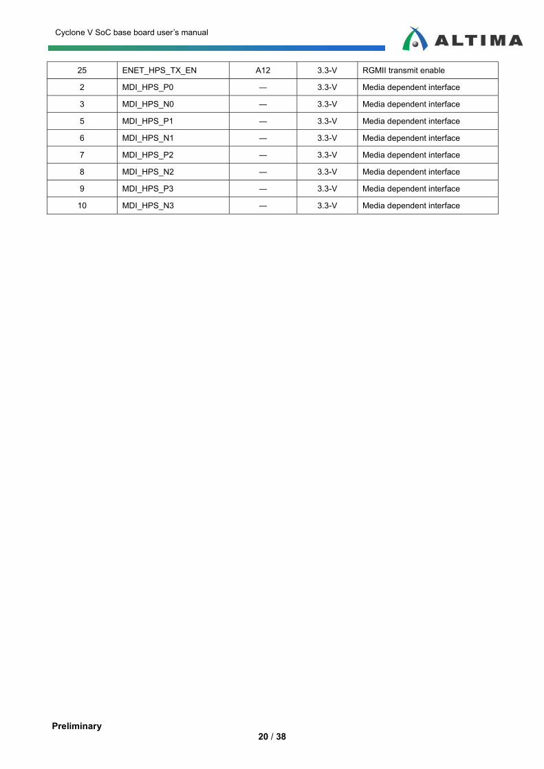
5.1. 10/100/1000 Ethernet Cyclone V SoC Base Board supports 10/100/1000 base-T Ethernet using an external Micrel
KSZ9021RL PHY and HPS Ethernet MAC function. The PHY-to-MAC interface is RGMII interface.
TheEthernet function must be provided in the FPGA for typical networking applications.
The Micrel KSZ9021RL PHY uses 3.3-V and 1.2-V power rails and requires a 25-MHz reference clock
driven from a dedicated oscillator.
Figure 6 shows the RGMII interface between the FPGA(MAC) and Micrel KSZ9021RL PHY.
Figure 6 RGMII Interface between FPGA(MAC) and Micrel KSZ9021RL PHY
Table 18 shows the Ethernet PHY interface pin assignments. Table 18 Ethernet PHY Pin assignments, Signal Names and Functions
Board
Reference(U18)
Schematic
Signal Name
Cyclone V Soc
Pin Number
I/O Standard Description
24 ENET_GTX_CLK J15 3.3-V 125-MHz RGMII transmit clock
38 ENET_HPS_INTn B14 3.3-V Management bus interrupt
17 ENET_HPS_LED1_LINK ― 3.3-V Programmable LED1 output
18 ENET_HPS_LED2_LINK ― 3.3-V Programmable LED2 output
36 ENET_HPS_MDC A13 3.3-V Management bus data clock
37 ENET_HPS_MDIO E16 3.3-V Management bus data
42 ENET_HPS_RESETn ― 3.3-V Device reset
35 ENET_HPS_RX_CLK J12 3.3-V RGMII receive clock
32 ENET_HPS_RXD0 A14 3.3-V RGMII receive data bus
31 ENET_HPS_RXD1 A11 3.3-V RGMII receive data bus
28 ENET_HPS_RXD2 C15 3.3-V RGMII receive data bus
27 ENET_HPS_RXD3 A9 3.3-V RGMII receive data bus
33 ENET_HPS_RX_DV J13 3.3-V RGMII receive data valid
19 ENET_HPS_TXD0 A16 3.3-V RGMII transmit data bus
20 ENET_HPS_TXD1 J14 3.3-V RGMII transmit data bus
21 ENET_HPS_TXD2 A15 3.3-V RGMII transmit data bus
22 ENET_HPS_TXD3 D17 3.3-V RGMII transmit data bus
Preliminary 20 / 38
Cyclone V SoC base board user’s manual
25 ENET_HPS_TX_EN A12 3.3-V RGMII transmit enable
2 MDI_HPS_P0 ― 3.3-V Media dependent interface
3 MDI_HPS_N0 ― 3.3-V Media dependent interface
5 MDI_HPS_P1 ― 3.3-V Media dependent interface
6 MDI_HPS_N1 ― 3.3-V Media dependent interface
7 MDI_HPS_P2 ― 3.3-V Media dependent interface
8 MDI_HPS_N2 ― 3.3-V Media dependent interface
9 MDI_HPS_P3 ― 3.3-V Media dependent interface
10 MDI_HPS_N3 ― 3.3-V Media dependent interface

Preliminary 21 / 38
Cyclone V SoC base board user’s manual
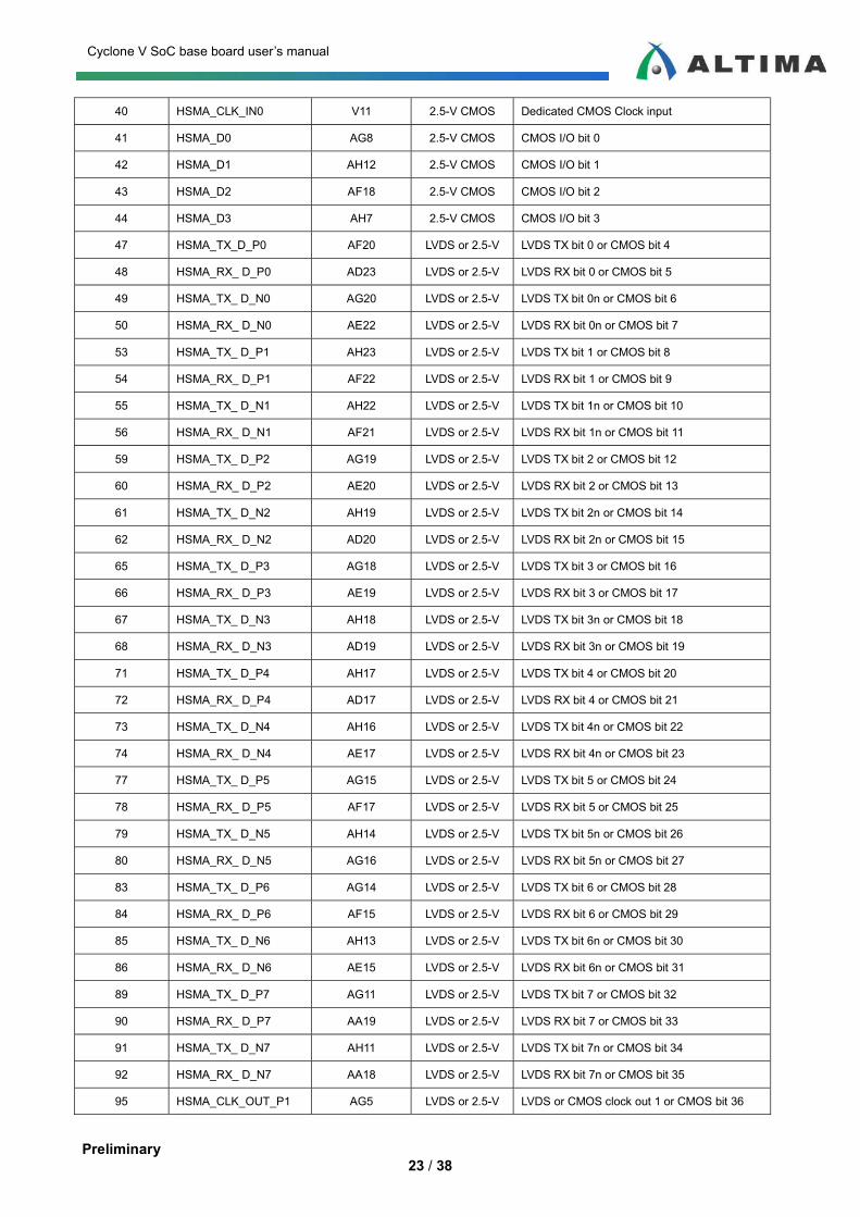
5.2. HSMC Cyclone V SoC Base Board supports a HSMC interface. This physical interface provides four channels
3.125 Gbps-capable transceivers. The HSMC interface also supports a full SPI4.2 interface (17 LVDS
channels), three input and output clocks, as well as JTAG and SMB signals. The LVDS channels can
be used for CMOS signaling or LVDS.
The HSMC is an Altera-developed open specification, which allows you to expand
functionality of Cyclone V SoC Base Board through the addition of daughter cards
For more information about the HSMC specification such as signaling standards,
signal integrity, compatible connectors, and mechanical information, refer to the High
Speed Mezzanine Card (HSMC) Specification manual.
The HSMC connector has a total of 172 pins, including 120 signal pins, 39 power pins,
and 13 ground pins. The ground pins are located between the two rows of signal and
power pins, acting both as a shield and a reference. The HSMC host connector is
the 0.5 mm-pitch QSH/QTH of high-speed, board-to-board
connectors supplied by Samtec. There are three banks in this connector. Bank 1 has every
third pin removed as done in the QSH-DP/QTH-DP series. Bank 2 and bank 3 have
all the pins populated as done in the QSH/QTH series.
Figure 7 shows the bank arrangement of signals with respect to the Samtec connector’s three banks.
Figure 7 HSMC Signal and Bank Diagram

Preliminary 22 / 38
Cyclone V SoC base board user’s manual
The HSMC interface has programmable bi-directional I/O pins that can be used as
2.5-V LVCMOS, which is 3.3-V LVTTL-compatible. These pins can also be used as
various differential I/O standards including, but not limited to, LVDS, mini-LVDS,
and RSDS with up to 17 full-duplex channels.
As noted in the High Speed Mezzanine Card (HSMC) Specification manual, LVDS and
single-ended I/O standards are only guaranteed to function when mixed according to
either the generic single-ended pin-out or generic differential pin-out.
Table 19 shows the HSMC interface pin assignments, signal names, and functions.
Table 19 HSMC Interface Pin Assignments, Schematic Signal Names, and Functions
Board
Reference(J4)
Schematic
Signal Name
Cyclone V Soc
Pin Number
I/O Standard Description
17 HSMA_TX_P3 D2 1.5-V PCML Transceiver TX bit 3
18 HSMA_RX_P3 F2 1.5-V PCML Transceiver RX bit 3
19 HSMA_TX_N3 D1 1.5-V PCML Transceiver TX bit 3n
20 HSMA_RX_N3 F1 1.5-V PCML Transceiver RX bit 3n
21 HSMA_TX_P2 H2 1.5-V PCML Transceiver TX bit 2
22 HSMA_RX_P2 K2 1.5-V PCML Transceiver RX bit 2
23 HSMA_TX_N2 H1 1.5-V PCML Transceiver TX bit 2n
24 HSMA_RX_N2 K1 1.5-V PCML Transceiver RX bit 2n
25 HSMA_TX_P1 M2 1.5-V PCML Transceiver TX bit 1
26 HSMA_RX_P1 P2 1.5-V PCML Transceiver RX bit 1
27 HSMA_TX_N1 M1 1.5-V PCML Transceiver TX bit 1n
28 HSMA_RX_N1 P1 1.5-V PCML Transceiver RX bit 1n
29 HSMA_TX_P0 T2 1.5-V PCML Transceiver TX bit 0
30 HSMA_RX_P0 V2 1.5-V PCML Transceiver RX bit 0
31 HSMA_TX_N0 T1 1.5-V PCML Transceiver TX bit 0n
32 HSMA_RX_N0 V1 1.5-V PCML Transceiver RX bit 0n
33 HSMA_SDA AA11 2.5-V CMOS Management serial data
34 HSMA_SCL Y11 2.5-V CMOS Management serial clock
35 JTAG_MUX_TCK ― 2.5-V CMOS JTAG clock signal
36 JTAG_HSMA_TMS ― 2.5-V CMOS JTAG mode select signal
37 JTAG_HSMA_TDO ― 2.5-V CMOS JTAG data output
38 JTAG_HSMA_TDI ― 2.5-V CMOS JTAG data input
39 HSMA_CLK_OUT0 AB26 2.5-V CMOS Dedicated CMOS Clock output
Preliminary 23 / 38
Cyclone V SoC base board user’s manual
40 HSMA_CLK_IN0 V11 2.5-V CMOS Dedicated CMOS Clock input
41 HSMA_D0 AG8 2.5-V CMOS CMOS I/O bit 0
42 HSMA_D1 AH12 2.5-V CMOS CMOS I/O bit 1
43 HSMA_D2 AF18 2.5-V CMOS CMOS I/O bit 2
44 HSMA_D3 AH7 2.5-V CMOS CMOS I/O bit 3
47 HSMA_TX_D_P0 AF20 LVDS or 2.5-V LVDS TX bit 0 or CMOS bit 4
48 HSMA_RX_ D_P0 AD23 LVDS or 2.5-V LVDS RX bit 0 or CMOS bit 5
49 HSMA_TX_ D_N0 AG20 LVDS or 2.5-V LVDS TX bit 0n or CMOS bit 6
50 HSMA_RX_ D_N0 AE22 LVDS or 2.5-V LVDS RX bit 0n or CMOS bit 7
53 HSMA_TX_ D_P1 AH23 LVDS or 2.5-V LVDS TX bit 1 or CMOS bit 8
54 HSMA_RX_ D_P1 AF22 LVDS or 2.5-V LVDS RX bit 1 or CMOS bit 9
55 HSMA_TX_ D_N1 AH22 LVDS or 2.5-V LVDS TX bit 1n or CMOS bit 10
56 HSMA_RX_ D_N1 AF21 LVDS or 2.5-V LVDS RX bit 1n or CMOS bit 11
59 HSMA_TX_ D_P2 AG19 LVDS or 2.5-V LVDS TX bit 2 or CMOS bit 12
60 HSMA_RX_ D_P2 AE20 LVDS or 2.5-V LVDS RX bit 2 or CMOS bit 13
61 HSMA_TX_ D_N2 AH19 LVDS or 2.5-V LVDS TX bit 2n or CMOS bit 14
62 HSMA_RX_ D_N2 AD20 LVDS or 2.5-V LVDS RX bit 2n or CMOS bit 15
65 HSMA_TX_ D_P3 AG18 LVDS or 2.5-V LVDS TX bit 3 or CMOS bit 16
66 HSMA_RX_ D_P3 AE19 LVDS or 2.5-V LVDS RX bit 3 or CMOS bit 17
67 HSMA_TX_ D_N3 AH18 LVDS or 2.5-V LVDS TX bit 3n or CMOS bit 18
68 HSMA_RX_ D_N3 AD19 LVDS or 2.5-V LVDS RX bit 3n or CMOS bit 19
71 HSMA_TX_ D_P4 AH17 LVDS or 2.5-V LVDS TX bit 4 or CMOS bit 20
72 HSMA_RX_ D_P4 AD17 LVDS or 2.5-V LVDS RX bit 4 or CMOS bit 21
73 HSMA_TX_ D_N4 AH16 LVDS or 2.5-V LVDS TX bit 4n or CMOS bit 22
74 HSMA_RX_ D_N4 AE17 LVDS or 2.5-V LVDS RX bit 4n or CMOS bit 23
77 HSMA_TX_ D_P5 AG15 LVDS or 2.5-V LVDS TX bit 5 or CMOS bit 24
78 HSMA_RX_ D_P5 AF17 LVDS or 2.5-V LVDS RX bit 5 or CMOS bit 25
79 HSMA_TX_ D_N5 AH14 LVDS or 2.5-V LVDS TX bit 5n or CMOS bit 26
80 HSMA_RX_ D_N5 AG16 LVDS or 2.5-V LVDS RX bit 5n or CMOS bit 27
83 HSMA_TX_ D_P6 AG14 LVDS or 2.5-V LVDS TX bit 6 or CMOS bit 28
84 HSMA_RX_ D_P6 AF15 LVDS or 2.5-V LVDS RX bit 6 or CMOS bit 29
85 HSMA_TX_ D_N6 AH13 LVDS or 2.5-V LVDS TX bit 6n or CMOS bit 30
86 HSMA_RX_ D_N6 AE15 LVDS or 2.5-V LVDS RX bit 6n or CMOS bit 31
89 HSMA_TX_ D_P7 AG11 LVDS or 2.5-V LVDS TX bit 7 or CMOS bit 32
90 HSMA_RX_ D_P7 AA19 LVDS or 2.5-V LVDS RX bit 7 or CMOS bit 33
91 HSMA_TX_ D_N7 AH11 LVDS or 2.5-V LVDS TX bit 7n or CMOS bit 34
92 HSMA_RX_ D_N7 AA18 LVDS or 2.5-V LVDS RX bit 7n or CMOS bit 35
95 HSMA_CLK_OUT_P1 AG5 LVDS or 2.5-V LVDS or CMOS clock out 1 or CMOS bit 36

Preliminary 24 / 38
Cyclone V SoC base board user’s manual
96 HSMA_CLK_IN_P1 W21 LVDS or 2.5-V LVDS or CMOS clock in 1 or CMOS bit 37
97 HSMA_CLK_OUT_N1 AH4 LVDS or 2.5-V LVDS or CMOS clock out 1n or CMOS bit 36
98 HSMA_CLK_IN_N1 W20 LVDS or 2.5-V LVDS or CMOS clock in 1n or CMOS bit 37
101 HSMA_TX_ D_P8 AG10 LVDS or 2.5-V LVDS TX bit 8 or CMOS bit 38
102 HSMA_RX_ D_P8 T11 LVDS or 2.5-V LVDS RX bit 8 or CMOS bit 39
103 HSMA_TX_ D_N8 AH9 LVDS or 2.5-V LVDS TX bit 8n or CMOS bit 40
104 HSMA_RX_ D_N8 U11 LVDS or 2.5-V LVDS RX bit 8n or CMOS bit 41
107 HSMA_TX_ D_P9 AG9 LVDS or 2.5-V LVDS TX bit 9 or CMOS bit 42
108 HSMA_RX_ D_P9 AE12 LVDS or 2.5-V LVDS RX bit 9 or CMOS bit 43
109 HSMA_TX_ D_N9 AH8 LVDS or 2.5-V LVDS TX bit 9n or CMOS bit 44
110 HSMA_RX_ D_N9 AD12 LVDS or 2.5-V LVDS RX bit 9n or CMOS bit 45
113 HSMA_TX_ D_P10 AH6 LVDS or 2.5-V LVDS TX bit 10 or CMOS bit 46
114 HSMA_RX_ D_P10 AG13 LVDS or 2.5-V LVDS RX bit 10 or CMOS bit 47
115 HSMA_TX_ D_N10 AH5 LVDS or 2.5-V LVDS TX bit 10n or CMOS bit 48
116 HSMA_RX_ D_N10 AF13 LVDS or 2.5-V LVDS RX bit 10n or CMOS bit 49
119 HSMA_TX_ D_P11 AH3 LVDS or 2.5-V LVDS TX bit 11 or CMOS bit 50
120 HSMA_RX_ D_P11 AD11 LVDS or 2.5-V LVDS RX bit 11 or CMOS bit 51
121 HSMA_TX_ D_N11 AH2 LVDS or 2.5-V LVDS TX bit 11n or CMOS bit 52
122 HSMA_RX_ D_N11 AE11 LVDS or 2.5-V LVDS RX bit 11n or CMOS bit 53
125 HSMA_TX_ D_P12 AE8 LVDS or 2.5-V LVDS TX bit 12 or CMOS bit 54
126 HSMA_RX_ D_P12 AF11 LVDS or 2.5-V LVDS RX bit 12 or CMOS bit 55
127 HSMA_TX_ D_N12 AF9 LVDS or 2.5-V LVDS TX bit 12n or CMOS bit 56
128 HSMA_RX_ D_N12 AF10 LVDS or 2.5-V LVDS RX bit 12n or CMOS bit 57
131 HSMA_TX_ D_P13 AE4 LVDS or 2.5-V LVDS TX bit 13 or CMOS bit 58
132 HSMA_RX_ D_P13 AD10 LVDS or 2.5-V LVDS RX bit 13 or CMOS bit 59
133 HSMA_TX_ D_N13 AF4 LVDS or 2.5-V LVDS TX bit 13n or CMOS bit 60
134 HSMA_RX_ D_N13 AE9 LVDS or 2.5-V LVDS RX bit 13n or CMOS bit 61
137 HSMA_TX_ D_P14 AF5 LVDS or 2.5-V LVDS TX bit 14 or CMOS bit 62
138 HSMA_RX_ D_P14 U14 LVDS or 2.5-V LVDS RX bit 14 or CMOS bit 63
139 HSMA_TX_ D_N14 AF6 LVDS or 2.5-V LVDS TX bit 14n or CMOS bit 64
140 HSMA_RX_ D_N14 U13 LVDS or 2.5-V LVDS RX bit 14n or CMOS bit 65
143 HSMA_TX_ D_P15 AE7 LVDS or 2.5-V LVDS TX bit 15 or CMOS bit 66
144 HSMA_RX_ D_P15 W14 LVDS or 2.5-V LVDS RX bit 15 or CMOS bit 67
145 HSMA_TX_ D_N15 AF8 LVDS or 2.5-V LVDS TX bit 15n or CMOS bit 68
146 HSMA_RX_ D_N15 V13 LVDS or 2.5-V LVDS RX bit 15n or CMOS bit 69
149 HSMA_TX_ D_P16 AF7 LVDS or 2.5-V LVDS TX bit 16 or CMOS bit 70
150 HSMA_RX_ D_P16 T13 LVDS or 2.5-V LVDS RX bit 16 or CMOS bit 71
151 HSMA_TX_ D_N16 AG6 LVDS or 2.5-V LVDS TX bit 16n or CMOS bit 72

Preliminary 25 / 38
Cyclone V SoC base board user’s manual
152 HSMA_RX_ D_N16 T12 LVDS or 2.5-V LVDS RX bit 16n or CMOS bit 73
155 HSMA_CLK_OUT_P2 E8 LVDS or 2.5-V LVDS or CMOS clock out 2 or CMOS bit 74
156 HSMA_CLK_IN_P2 E11 LVDS or 2.5-V LVDS or CMOS clock in 2 or CMOS bit 75
157 HSMA_CLK_OUT_N2 D8 LVDS or 2.5-V LVDS or CMOS clock out 2n or CMOS bit 76
158 HSMA_CLK_IN_N2 D11 LVDS or 2.5-V LVDS or CMOS clock in 2n or CMOS bit 77
160 HSMA_PSNTN AD5 2.5-V CMOS HSMC port presence detect

Preliminary 26 / 38
Cyclone V SoC base board user’s manual
5.3. USB2.0 OTG Cyclone V SoC Base Board supports USB 2.0 OTG using an external SMSC USB3300 PHY and
HPS ULPI LINK function. The PHY-to-LINK interface is ULPI interface. The LINK function must
be provided in the FPGA for typical USB applications.
Figure 8 shows the ULPI interface between the FPGA (LINK) and SMSC USB3300 PHY.
Figure 8 ULPI Interface between FPGA (LINK) and SMSC USB3300 PHY
Table 20 shows the ULPI interface between the FPGA (LINK) and SMSC USB3300 PHY.
Table 20 USB2.0 PHY Pin Assignments, Signal Names and Functions
Board
Reference(U25)
Schematic
Signal Name
Cyclone V Soc
Pin Number
I/O Standard Description
14 USB_CLK G4 3.3-V ULPI Clock
24 USB_DATA0 C10 3.3-V ULPI Data Bit 0
23 USB_DATA1 F5 3.3-V ULPI Data Bit 1
22 USB_DATA2 C9 3.3-V ULPI Data Bit 2
21 USB_DATA3 C4 3.3-V ULPI Data Bit 3
20 USB_DATA4 C8 3.3-V ULPI Data Bit 4
19 USB_DATA5 D4 3.3-V ULPI Data Bit 5
18 USB_DATA6 C7 3.3-V ULPI Data Bit 6
17 USB_DATA7 F4 3.3-V ULPI Data Bit 7
12 USB_DIR E5 3.3-V ULPI DIrection
11 USB_NXT D5 3.3-V ULPI Next Data
13 USB_STP C5 3.3-V ULPI Stop Data
9 USB_RESET E4 3.3-V Optional Active High Reset.

Preliminary 27 / 38
Cyclone V SoC base board user’s manual
5.4. UART Cyclone V SoC Base Board supports USB/UART using an external Silicon Labs CP2104 and
HPS UART function.
Table 21 lists the UART interface between the FPGA and Silicon Labs CP2104 PHY.
Table 21 USB to UART IC Pin Assignments, Signal Names and Functions
Board
Reference(U28)
Schematic
Signal Name
Cyclone V Soc
Pin Number
I/O Standard Description
21 UART_RX B19 3.3-V UART Receive
20 UART_TX C16 3.3-V UART Transmit
12 CONV_HPS_USB_N C6 3.3-V T.B.D.
5.5. SD Cyclone V SoC Base Board supports Micro SD.
Table 22 lists the Micro SD interface between the FPGA and Micro SD Socket.
Table 22 SD Pin Assignments, Signal Names and Functions
Board
Reference(J7)
Schematic
Signal Name
Cyclone V Soc
Pin Number
I/O Standard Description
5 SD_CLK B8 3.3-V SDMMC Clock out
3 SD_CMD D14 3.3-V SDMMC Command Line
7 SD_DAT0 C13 3.3-V SDMMC Data Bit 0
8 SD_DAT1 B6 3.3-V SDMMC Data Bit 1
1 SD_DAT2 B11 3.3-V SDMMC Data Bit 2
2 SD_CD_DAT3 B9 3.3-V SDMMC Data Bit 3

Preliminary 28 / 38
Cyclone V SoC base board user’s manual
5.6. I2C Cyclone V SoC Base Board supports I2C Interface.
Table 24 lists the I2C Interface pin assignments, signal names, and functions.
Table 25 lists the I2C connected devices.
Table 23 I2C Pin Assignments, Signal Names and Functions
Schematic
Signal Name
Cyclone V Soc
Pin Number
I/O Standard Description
I2C_SCL_HPS B16 3.3-V I2C Clock
I2C_SDA_HPS C19 3.3-V I2C Data
I2C_SCL_FPGA AA24 2.5-V I2C Clock
I2C_SDA_FPGA AA23 2.5-V I2C Data
Table 24 I2C connected devices
Board Reference Type Device Address Description
U19 24LC32A 0x51 EEPROM
U27 DS1339C-33 0x68 RTC
U34 LTC2978 0x5C Power Monitor IC

Preliminary 29 / 38
Cyclone V SoC base board user’s manual
6. Memory
6.1. DDR3 SDRAM Cyclone V SoC Base Board supports two 8Mx16x8 interfaces for high-speed sequential memory
access. User can use hard memory controller (HPS on the top edge of the FPGA) to run DDR3
SDRAM memory.
Each 32-bit data bus comprises of two x16 devices.
Table 25 and Table 26 lists DDR3-SDRAM pin assignments, signal names and functions. The signal
names and types are relative to the Cyclone V SoC in terms of I/O setting and direction.
Table 25 DDR3 Device #1 Pin Assignments, Schematic Signal Names and Functions
Board
Reference(U17)
Schematic
Signal Name
Cyclone V Soc
Pin Number
I/O Standard Description
N3 DDR3_HPS_A0 C28 1.5V-SSTL Class I Address bus
P7 DDR3_HPS_A1 B28 1.5V-SSTL Class I Address bus
P3 DDR3_HPS_A2 E26 1.5V-SSTL Class I Address bus
N2 DDR3_HPS_A3 D26 1.5V-SSTL Class I Address bus
P8 DDR3_HPS_A4 J21 1.5V-SSTL Class I Address bus
P2 DDR3_HPS_A5 J20 1.5V-SSTL Class I Address bus
R8 DDR3_HPS_A6 C26 1.5V-SSTL Class I Address bus
R2 DDR3_HPS_A7 B26 1.5V-SSTL Class I Address bus
T8 DDR3_HPS_A8 F26 1.5V-SSTL Class I Address bus
R3 DDR3_HPS_A9 F25 1.5V-SSTL Class I Address bus
L7 DDR3_HPS_A10 A24 1.5V-SSTL Class I Address bus
R7 DDR3_HPS_A11 B24 1.5V-SSTL Class I Address bus
N7 DDR3_HPS_A12 D24 1.5V-SSTL Class I Address bus
M2 DDR3_HPS_BA0 A27 1.5V-SSTL Class I Bank Address bus
N8 DDR3_HPS_BA1 H25 1.5V-SSTL Class I Bank Address bus
M3 DDR3_HPS_BA2 G25 1.5V-SSTL Class I Bank Address bus
L2 DDR3_HPS_CSn L21 1.5V-SSTL Class I Chip select
L3 DDR3_HPS_WEn E25 1.5V-SSTL Class I
J3 DDR3_HPS_RASn A25 1.5V-SSTL Class I Row address select
K3 DDR3_HPS_CASn A26 1.5V-SSTL Class I Column address select
K9 DDR3_HPS_CKE L28 1.5V-SSTL Class I
J7 DDR3_HPS_CLK_P N21 Differential 1.5-V
SSTL Class I
Differential clock
K7 DDR3_HPS_CLK_N N20 Differential 1.5-V Differential clock

Preliminary 30 / 38
Cyclone V SoC base board user’s manual
SSTL Class I
E7 DDR3_HPS_DM0 G28 1.5V-SSTL Class I Write mask byte lane
D3 DDR3_HPS_DM1 P28 1.5V-SSTL Class I Write mask byte lane
H8 DDR3_HPS_DQ0 J25 1.5V-SSTL Class I Data bus byte lane 0
H7 DDR3_HPS_DQ1 J24 1.5V-SSTL Class I Data bus byte lane 0
E3 DDR3_HPS_DQ2 E28 1.5V-SSTL Class I Data bus byte lane 0
H3 DDR3_HPS_DQ3 D27 1.5V-SSTL Class I Data bus byte lane 0
F7 DDR3_HPS_DQ4 J26 1.5V-SSTL Class I Data bus byte lane 0
F8 DDR3_HPS_DQ5 K26 1.5V-SSTL Class I Data bus byte lane 0
G2 DDR3_HPS_DQ6 G27 1.5V-SSTL Class I Data bus byte lane 0
F2 DDR3_HPS_DQ7 F28 1.5V-SSTL Class I Data bus byte lane 0
C8 DDR3_HPS_DQ8 K25 1.5V-SSTL Class I Data bus byte lane 1
B8 DDR3_HPS_DQ9 L25 1.5V-SSTL Class I Data bus byte lane 1
D7 DDR3_HPS_DQ10 J27 1.5V-SSTL Class I Data bus byte lane 1
A7 DDR3_HPS_DQ11 J28 1.5V-SSTL Class I Data bus byte lane 1
C2 DDR3_HPS_DQ12 M27 1.5V-SSTL Class I Data bus byte lane 1
C3 DDR3_HPS_DQ13 M26 1.5V-SSTL Class I Data bus byte lane 1
A3 DDR3_HPS_DQ14 M28 1.5V-SSTL Class I Data bus byte lane 1
A2 DDR3_HPS_DQ15 N28 1.5V-SSTL Class I Data bus byte lane 1
F3 DDR3_HPS_DQS_P0 R17 Differential 1.5-V
SSTL Class I
Data strobe P byte lane 0
G3 DDR3_HPS_DQS_N0 R16 Differential 1.5-V
SSTL Class I
Data strobe N byte lane 0
C7 DDR3_HPS_DQS_P1 R19 Differential 1.5-V
SSTL Class I
Data strobe P byte lane 1
B7 DDR3_HPS_DQS_N1 R18 Differential 1.5-V
SSTL Class I
Data strobe N byte lane 1
K1 DDR3_HPS_ODT D28 1.5V-SSTL Class I On-die termination enable
L8 DDR3_HPS_ZQ ― ― ZQ impedance calibration

Preliminary 31 / 38
Cyclone V SoC base board user’s manual
Table 26 DDR3 Device #2 Pin Assignments, Schematic Signal Names and Functions
Board
Reference(U16)
Schematic
Signal Name
Cyclone V Soc
Pin Number
I/O Standard Description
N3 DDR3_HPS_A0 C28 1.5V-SSTL Class I Address bus
P7 DDR3_HPS_A1 B28 1.5V-SSTL Class I Address bus
P3 DDR3_HPS_A2 E26 1.5V-SSTL Class I Address bus
N2 DDR3_HPS_A3 D26 1.5V-SSTL Class I Address bus
P8 DDR3_HPS_A4 J21 1.5V-SSTL Class I Address bus
P2 DDR3_HPS_A5 J20 1.5V-SSTL Class I Address bus
R8 DDR3_HPS_A6 C26 1.5V-SSTL Class I Address bus
R2 DDR3_HPS_A7 B26 1.5V-SSTL Class I Address bus
T8 DDR3_HPS_A8 F26 1.5V-SSTL Class I Address bus
R3 DDR3_HPS_A9 F25 1.5V-SSTL Class I Address bus
L7 DDR3_HPS_A10 A24 1.5V-SSTL Class I Address bus
R7 DDR3_HPS_A11 B24 1.5V-SSTL Class I Address bus
N7 DDR3_HPS_A12 D24 1.5V-SSTL Class I Address bus
M2 DDR3_HPS_BA0 A27 1.5V-SSTL Class I Bank Address bus
N8 DDR3_HPS_BA1 H25 1.5V-SSTL Class I Bank Address bus
M3 DDR3_HPS_BA2 G25 1.5V-SSTL Class I Bank Address bus
L2 DDR3_HPS_CSn L21 1.5V-SSTL Class I Chip select
L3 DDR3_HPS_WEn E25 1.5V-SSTL Class I
J3 DDR3_HPS_RASn A25 1.5V-SSTL Class I Row address select
K3 DDR3_HPS_CASn A26 1.5V-SSTL Class I Column address select
K9 DDR3_HPS_CKE L28 1.5V-SSTL Class I
J7 DDR3_HPS_CLK_P N21 Differential 1.5-V
SSTL Class I
Differential clock
K7 DDR3_HPS_CLK_N N20 Differential 1.5-V
SSTL Class I
Differential clock
E7 DDR3_HPS_DM2 W28 1.5V-SSTL Class I Write mask byte lane
D3 DDR3_HPS_DM3 AB28 1.5V-SSTL Class I Write mask byte lane
H8 DDR3_HPS_DQ16 N24 1.5V-SSTL Class I Data bus byte lane 0
H7 DDR3_HPS_DQ17 N25 1.5V-SSTL Class I Data bus byte lane 0
E3 DDR3_HPS_DQ18 T28 1.5V-SSTL Class I Data bus byte lane 0
H3 DDR3_HPS_DQ19 U28 1.5V-SSTL Class I Data bus byte lane 0
F7 DDR3_HPS_DQ20 N26 1.5V-SSTL Class I Data bus byte lane 0
F8 DDR3_HPS_DQ21 N27 1.5V-SSTL Class I Data bus byte lane 0
G2 DDR3_HPS_DQ22 R27 1.5V-SSTL Class I Data bus byte lane 0

Preliminary 32 / 38
Cyclone V SoC base board user’s manual
F2 DDR3_HPS_DQ23 V27 1.5V-SSTL Class I Data bus byte lane 0
C8 DDR3_HPS_DQ24 R26 1.5V-SSTL Class I Data bus byte lane 1
B8 DDR3_HPS_DQ25 R25 1.5V-SSTL Class I Data bus byte lane 1
D7 DDR3_HPS_DQ26 AA28 1.5V-SSTL Class I Data bus byte lane 1
A7 DDR3_HPS_DQ27 W26 1.5V-SSTL Class I Data bus byte lane 1
C2 DDR3_HPS_DQ28 R24 1.5V-SSTL Class I Data bus byte lane 1
C3 DDR3_HPS_DQ29 T24 1.5V-SSTL Class I Data bus byte lane 1
A3 DDR3_HPS_DQ30 Y27 1.5V-SSTL Class I Data bus byte lane 1
A2 DDR3_HPS_DQ31 AA27 1.5V-SSTL Class I Data bus byte lane 1
F3 DDR3_HPS_DQS_P2 T19 Differential 1.5-V
SSTL Class I
Data strobe P byte lane 0
G3 DDR3_HPS_DQS_N2 T18 Differential 1.5-V
SSTL Class I
Data strobe N byte lane 0
C7 DDR3_HPS_DQS_P3 U19 Differential 1.5-V
SSTL Class I
Data strobe P byte lane 1
B7 DDR3_HPS_DQS_N3 T20 Differential 1.5-V
SSTL Class I
Data strobe N byte lane 1
K1 DDR3_HPS_ODT D28 1.5V-SSTL Class I On-die termination enable
L8 DDR3_HPS_ZQ ― ― ZQ impedance calibration
6.2. QSPI FlashROM Cyclone V SoC Base Board supports a 512Mbit Quad-SPI flash device for non-volatile storage of user
code space.
Table 27 shows the Quad-SPI flash device pin assignments, signal names an functions. The signal
names and types are relative to the Cyclone V SoC in terms of I/O setting and direction.
Table 27 Quad-SPI Flash Pin Assignments, Schematic Signal Names and Functions
Board
Reference(U*)
Schematic
Signal Name
Cyclone V Soc
Pin Number
I/O Standard Description
16 QSPI_CLK C14 2.5-V QSPI Clock
15 QSPI_IO0 A8 2.5-V QSPI Data IO Bit 0
8 QSPI_IO1 H16 2.5-V QSPI Data IO Bit 1
9 QSPI_IO2 A7 2.5-V QSPI Data IO Bit 2
1 QSPI_IO3 J16 2.5-V QSPI Data IO Bit 3
7 QSPI_SS0 A6 2.5-V QSPI Slave Select 0

Preliminary 33 / 38
Cyclone V SoC base board user’s manual
7. Power Supply
7.1. Power Distribution System
Table 28 lists the power estimate.
Table 28 Cyclone V SoC FPGA Base Board Power Estimate
3.3V_EXT 3.3V Units:mAProduct Part Name 1.2V 3.3V 1.1V 1.5V 2.5V 3.3V 0.75V 1.8V 5.0V 12V Note
CycloneV FPGA 5CXFC6U23 2000 330 51825 300 100 20 1 HPS & Transciever Power
MAXII CPLD EPM570GF100 1 5 50Configuration ROM EPCQ256S16N 20DDR3 SDRAM MT41J64M16 660 2 IDD7, 2unitsQSPI Flash N25Q00AA13GSF40F 20 eraseEthernet PHY KSZ9021RN 563 133EEPROM 24LC32A-I/SN 3MicroSD MicroSD Card 200 External devicesUSB2.0 OTG PHY USB3300 41.6 46.8USB2.0 OTG Port USB Device 500 External devicesUSB2.0 PHY CY7C68013A 50UART to USB CP2104 18.5RTC DS1339C 5HSMC 2000 1000PLL Si52112 HSMC Host side minimam currentOSC 125MHz EG-2121CA 30OSC 100MHz 30OSC 50MHz 30LCD NHD-0216K3Z-NSW-BBW-V3 247FAN 160Total 563 2000 3825 960 524 518 3 97 747 1160Ethernet PHY Power LTC3026-1 → 563DDR3 VTT, VREF TPS51200 3 ←DCDC LTC3605EUF → 632 efficiency = 87%DCDC LTC3605EUF → 150 efficiency = 80%DCDC LTC3605EUF → 260 efficiency = 87%DCDC LTC3613EWKH_6 → 403 efficiency = 87%DCDC LTC3613EWKH_6 → 164 efficiency = 87%Primary circuit total with HSMC 2770 33WPrimary circuit total w/o HSMC 1138 14W
Preliminary 34 / 38
Cyclone V SoC base board user’s manual
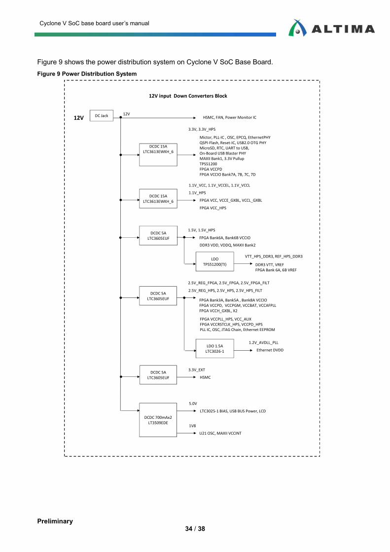
Figure 9 shows the power distribution system on Cyclone V SoC Base Board. Figure 9 Power Distribution System
3.3V, 3.3V_HPS
12V12V
DCDC 15ALTC3613EWKH_6
1.1V_VCC, 1.1V_VCCEL, 1.1V_VCCL
FPGA VCC, VCCE_GXBL, VCCL_GXBL
DCDC 5ALTC3605EUF FPGA Bank6A, Bank6B VCCIO
DCDC 5ALTC3605EUF FPGA Bank3A, Bank5A , Bank8A VCCIO
FPGA VCCPD, VCCPGM, VCCBAT, VCCAFPLLFPGA VCCH_GXBL, X2
2.5V_REG_FPGA, 2.5V_FPGA, 2.5V_FPGA_FILT
FPGA VCCPLL_HPS, VCC_AUXFPGA VCCRSTCLK_HPS, VCCPD_HPSPLL IC, OSC, JTAG Chain, Ethernet EEPROM
2.5V_REG_HPS, 2.5V_HPS, 2.5V_HPS_FILT
LDO 1.5ALTC3026-1
1.2V_AVDLL_PLL
Ethernet DVDD
DDR3 VDD, VDDQ, MAXII Bank2
1.5V, 1.5V_HPS
LDOTPS51200(TI) DDR3 VTT, VREF
FPGA Bank 6A, 6B VREF
VTT_HPS_DDR3, REF_HPS_DDR3
DCDC 5ALTC3605EUF HSMC
3.3V_EXT
FPGA VCC_HPS
1.1V_HPS
DCDC 700mAx2LT3509EDE
LTC3025-1 BIAS, USB BUS Power, LCD
5.0V
1V8
U21 OSC, MAXII VCCINT
HSMC, FAN, Power Monitor IC
Mictor, PLL-IC , OSC, EPCQ, EthernetPHYQSPI-Flash, Reset-IC, USB2.0 OTG PHYMicroSD, RTC, UART to USB,On-Board USB Blaster PHYMAXII Bank1, 3.3V PullupTPS51200FPGA VCCPDFPGA VCCIO Bank7A, 7B, 7C, 7D
12V input Down Converters Block
DCDC 15ALTC3613EWKH_6
DC Jack