CY3650 USB Development System User’ s Guide Sheets/Cypress PDFs/CY3650.pdf · PC Development...
14
CY3650 USB Development System User’s Guide Version 2.4 June 30, 1999
Transcript of CY3650 USB Development System User’ s Guide Sheets/Cypress PDFs/CY3650.pdf · PC Development...
CY3650USB Development System
User’s Guide
Version 2.4
June 30, 1999
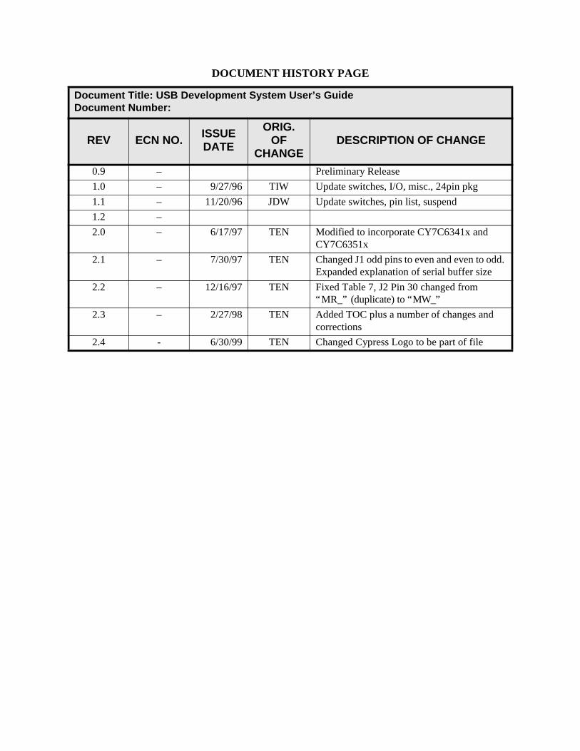
DOCUMENT HISTORY PAGE
Document Title: USB Development System User’s GuideDocument Number:
REV ECN NO. ISSUE DATE
ORIG. OF
CHANGEDESCRIPTION OF CHANGE
0.9 – Preliminary Release1.0 – 9/27/96 TIW Update switches, I/O, misc., 24pin pkg1.1 – 11/20/96 JDW Update switches, pin list, suspend1.2 –2.0 – 6/17/97 TEN Modified to incorporate CY7C6341x and
CY7C6351x2.1 – 7/30/97 TEN Changed J1 odd pins to even and even to odd.
Expanded explanation of serial buffer size 2.2 – 12/16/97 TEN Fixed Table 7, J2 Pin 30 changed from
“MR_” (duplicate) to “MW_”2.3 – 2/27/98 TEN Added TOC plus a number of changes and
corrections2.4 - 6/30/99 TEN Changed Cypress Logo to be part of file
Ver 2.4 – i –
CY3650 USB Development System User’s Guide
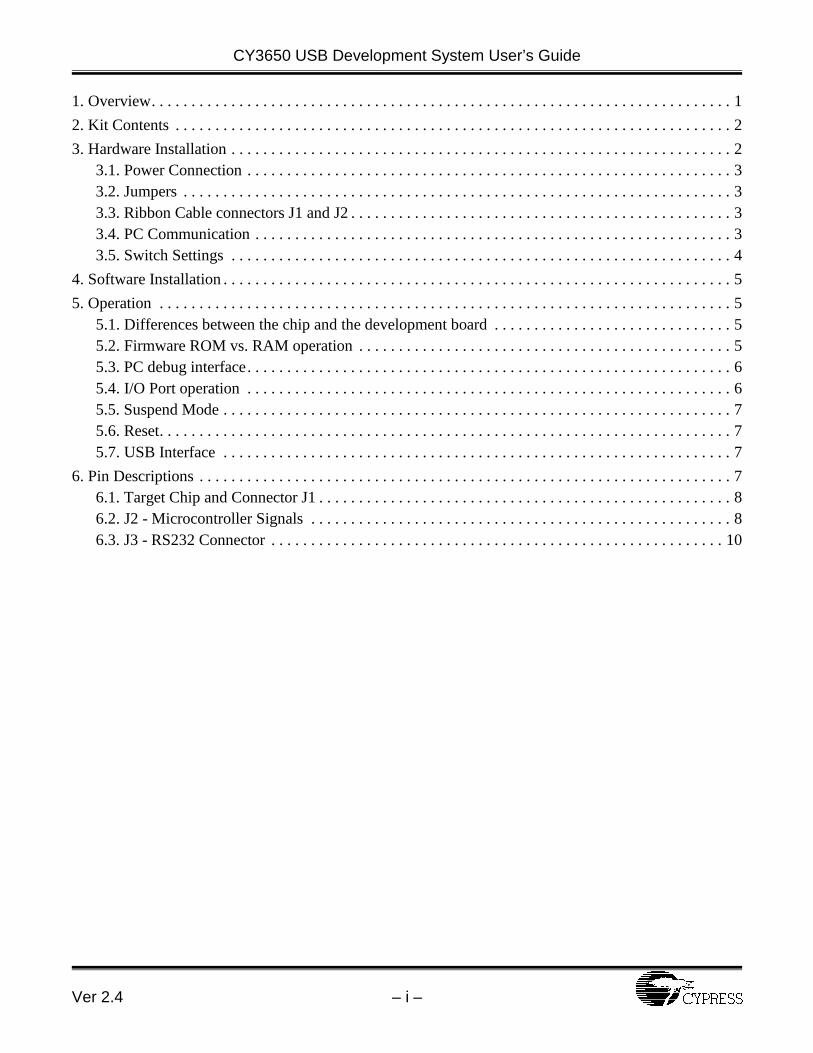
1. Overview. . . . . . . . . . . . . . . . . . . . . . . . . . . . . . . . . . . . . . . . . . . . . . . . . . . . . . . . . . . . . . . . . . . . . . . . . 12. Kit Contents . . . . . . . . . . . . . . . . . . . . . . . . . . . . . . . . . . . . . . . . . . . . . . . . . . . . . . . . . . . . . . . . . . . . . . 23. Hardware Installation . . . . . . . . . . . . . . . . . . . . . . . . . . . . . . . . . . . . . . . . . . . . . . . . . . . . . . . . . . . . . . . 2
3.1. Power Connection . . . . . . . . . . . . . . . . . . . . . . . . . . . . . . . . . . . . . . . . . . . . . . . . . . . . . . . . . . . . . 33.2. Jumpers . . . . . . . . . . . . . . . . . . . . . . . . . . . . . . . . . . . . . . . . . . . . . . . . . . . . . . . . . . . . . . . . . . . . . 33.3. Ribbon Cable connectors J1 and J2 . . . . . . . . . . . . . . . . . . . . . . . . . . . . . . . . . . . . . . . . . . . . . . . . 33.4. PC Communication . . . . . . . . . . . . . . . . . . . . . . . . . . . . . . . . . . . . . . . . . . . . . . . . . . . . . . . . . . . . 33.5. Switch Settings . . . . . . . . . . . . . . . . . . . . . . . . . . . . . . . . . . . . . . . . . . . . . . . . . . . . . . . . . . . . . . . 4
4. Software Installation . . . . . . . . . . . . . . . . . . . . . . . . . . . . . . . . . . . . . . . . . . . . . . . . . . . . . . . . . . . . . . . . 55. Operation . . . . . . . . . . . . . . . . . . . . . . . . . . . . . . . . . . . . . . . . . . . . . . . . . . . . . . . . . . . . . . . . . . . . . . . . 5
5.1. Differences between the chip and the development board . . . . . . . . . . . . . . . . . . . . . . . . . . . . . . 55.2. Firmware ROM vs. RAM operation . . . . . . . . . . . . . . . . . . . . . . . . . . . . . . . . . . . . . . . . . . . . . . . 55.3. PC debug interface. . . . . . . . . . . . . . . . . . . . . . . . . . . . . . . . . . . . . . . . . . . . . . . . . . . . . . . . . . . . . 65.4. I/O Port operation . . . . . . . . . . . . . . . . . . . . . . . . . . . . . . . . . . . . . . . . . . . . . . . . . . . . . . . . . . . . . 65.5. Suspend Mode . . . . . . . . . . . . . . . . . . . . . . . . . . . . . . . . . . . . . . . . . . . . . . . . . . . . . . . . . . . . . . . . 75.6. Reset. . . . . . . . . . . . . . . . . . . . . . . . . . . . . . . . . . . . . . . . . . . . . . . . . . . . . . . . . . . . . . . . . . . . . . . . 75.7. USB Interface . . . . . . . . . . . . . . . . . . . . . . . . . . . . . . . . . . . . . . . . . . . . . . . . . . . . . . . . . . . . . . . . 7
6. Pin Descriptions . . . . . . . . . . . . . . . . . . . . . . . . . . . . . . . . . . . . . . . . . . . . . . . . . . . . . . . . . . . . . . . . . . . 76.1. Target Chip and Connector J1 . . . . . . . . . . . . . . . . . . . . . . . . . . . . . . . . . . . . . . . . . . . . . . . . . . . . 86.2. J2 - Microcontroller Signals . . . . . . . . . . . . . . . . . . . . . . . . . . . . . . . . . . . . . . . . . . . . . . . . . . . . . 86.3. J3 - RS232 Connector . . . . . . . . . . . . . . . . . . . . . . . . . . . . . . . . . . . . . . . . . . . . . . . . . . . . . . . . . 10

– ii – Ver 2.4
CY3650 USB Development System User’s Guide

Ver 2.4 – 1 –
CY3650 USB Development System User’s Guide
1. OverviewThe Cypress USB Development System is a powerful tool to assist development of user hardware and firmwarewith emulated Cypress USB ICs. In the full development system environment (Figure 1), a PC-based interfacefacilitates debugging through break-traps, single stepping, and display/modification of registers and data RAM. Inthis mode, firmware can be implemented in on-board EPROM, or downloaded to program RAM. The RAM optionprovides a quick and easy method for testing firmware revisions.
Stand-alone mode (Figure 2) allows portable system operation. In this case, user firmware is loaded in EPROM,and only power need be applied to produce a fully operating emulated USB chip.
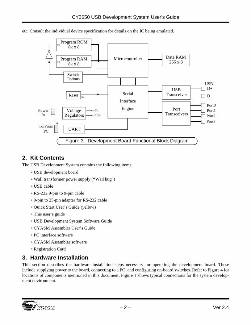
Figure 3 shows a block diagram of the development board, illustrating the major system components and the userinterfaces. The board supports a family of Cypress USB ICs, with varying amounts of on-chip EPROM, RAM, I/O,
PC
DevelopmentBoard
Logic Analyzer
Target System
Wall Bug
USB
RS-232
J1J2
Figure 1. Typical USB Development Environment
DevelopmentBoard
Target System
Wall Bug
Figure 2. Stand-alone Environment
J2 J1
– 2 – Ver 2.4
CY3650 USB Development System User’s Guide
etc. Consult the individual device specification for details on the IC being emulated.
2. Kit ContentsThe USB Development System contains the following items:
• USB development board• Wall transformer power supply (“Wall bug”)• USB cable• RS-232 9-pin to 9-pin cable• 9-pin to 25-pin adapter for RS-232 cable• Quick Start User’s Guide (yellow)• This user’s guide• USB Development System Software Guide• CYASM Assembler User’s Guide• PC interface software• CYASM Assembler software• Registration Card
3. Hardware InstallationThis section describes the hardware installation steps necessary for operating the development board. Theseinclude supplying power to the board, connecting to a PC, and configuring on-board switches. Refer to Figure 4 forlocations of components mentioned in this document; Figure 1 shows typical connections for the system develop-ment environment.
To/From PC
Serial
Interface
Engine
CS
CS
USBD+
D−
J6
J13PowerIn
+5V
Reset
SwitchOptions
Program RAM8k x 8
Program ROM8k x 8
Data RAM256 x 8
UART
USBTransceiver
Microcontroller
S2
VoltageRegulators +3.3V
PortTransceivers
Port0Port1Port2Port3
Figure 3. Development Board Functional Block Diagram

Ver 2.4 – 3 –
CY3650 USB Development System User’s Guide
3.1. Power ConnectionThe development board is designed to be powered by the enclosed wall transformer. Connect the transformer to a110V AC source, and to power jack J13 on the board. +5V and +3.3V are generated by regulators on the board.The green LED will light when power is applied.
3.2. JumpersJumper JP1, at the right side of Figure 4, applies VDD (+5V) to pin 57 of connector J1. Without JP1, no connectionto VDD occurs on J1. The board is shipped with the jumper installed.
3.3. Ribbon Cable connectors J1 and J2The diagram above correctly depicts the location of pin 1 for both J1 and J2. However the printed wiring boardshows J1 pin 1 incorrectly. Please refer to figure 4 when locating pin numbers.
3.4. PC CommunicationFor communicating with a PC, plug the enclosed RS-232 cable into the 9-pin connector J6 on the board. The otherend of the cable should be connected to the appropriate COM port on the PC, typically COM1 or COM2, depend-ing on the PC’s configuration. A 9-pin to 25-pin adapter is provided in case the PC port uses a 25-pin connector.
Cypress Semiconductor
1/12/97 Rev B
P/N MPU-80-EMU
JP1
JP2
RS3
RS
11R
S9
RS
7R
S5
RS
8R
S6
RS
4R
S10
J1
C51
U7J12
U11
R1
D3
D4
D5
D6
D7
D8
D9
D10
J8
R5
D2
D1
R4
C25C45
U12
S2
U10
J10
RP1
U3
RS1
J7
U2
U15
U14
U13
U8
U5
J2
U1
J13
C52
C53
J9
U6
J6
U9
S3
RS2
U4
J11
Figure 4. Development Board Layout
(Use
r EP
RO
M)
D11
S1
USB Conn.

– 4 – Ver 2.4
CY3650 USB Development System User’s Guide
The required communication settings for the PC are:
It is also recommended that the UART FIFO size settings be set to the minimum values. In Windows 95 the follow-ing steps will change the FIFO settings:
• On the desk-top, double click on the “My Computer” Icon and then double click on the “Control Panel” Icon. Alter-nately, use the “start” menu and choose “Settings” and then “Control Panel”.
• In the “Control Panel” window, double click on the “System” Icon.
• In the “System” window click on the “Device Manager” tab. Then scroll down through the list of devices to the serialport used for the USB Development Board, this is usually COM1 or COM2. Select the appropriate device by doubleclicking.
• This brings up a serial device window, inside you will see tabs, select the “Advanced” tab. This sub-widow contain thesettings for the serial transmit and receive FIFOs. Set the receive FIFO to 1 and set the transmit FIFO to 3 if this is avalid setting, otherwise set the FIFO size to 1.
3.5. Switch SettingsTwo 8-position DIP switches provide configuration options for the two on-board FPGAs. Table 1 and Table 2 listoptions for switches S1 and S3 respectively. Further information on these options is given in Section 5. Unusedswitches should be left in the default setting, as these may support internal test modes.
Baud Rate 19200
Data Bits 8
Parity None
Stop Bits 1
Flow Control None used
Table 1: Switch S1 ConfigurationPosition Open (1) Closed (0) Function
1 Enable Disable USB Bus Reset2 Enable Disable Watch Dog Reset3 Enable Disable Cext (wake up)4 Enable Disable IO Port Input Only Mode5 Enable Disable Suspend on Power On Reset6 Default – Required7 Default – Required8 Default – Required

Ver 2.4 – 5 –
CY3650 USB Development System User’s Guide
4. Software InstallationFor information on operation of the interactive PC debug environment, refer to the USB Development SystemSoftware Guide.
For information on the CYASM assembly language programming and the assembler, refer to the CYASM Assem-bler User’s Guide.
5. Operation
5.1. Differences between the chip and the development boardThe development board is lacking some of the features that are present on the integrated circuit. Three importantdifferences are:
1. No programmable pull-up resistors on GPIO pins2. No programmable DAC currents on GPIO pins3. The development board is not bus powered and therefore it is not initialized when the USB connector is
first attached.
5.2. Firmware ROM vs. RAM operationThe user’s program code will be executed from either a ROM (U5) or program RAM, depending on the setting ofswitch S3-1 (see Table 2). The U5 ROM is a Cypress CY7C261-45, an 8k x 8 UV-erasable EPROM. Only 4k ofthe EPROM is currently addressable. The program RAM supports the same memory size as the EPROM.
To program or erase the EPROM, refer to the data sheets for the Cypress CY7C261-45. The part can be repeatedlyreprogrammed as user firmware is updated. Follow appropriate ESD precautions when handling the part. Wheninstalling U5 in the development board, note the IC orientation guide, shown on the board and in Figure 4.
The following examples illustrate typical procedures for operating from either ROM or RAM.
Example 1: Program ROM Operation
1. Develop assembly code; program this into the U5 Cypress CY7C261-45 EPROM.2. Remove power from the development board.3. Install U5 into the development board.4. Set switch S3-1 for program ROM operation (see Table 2)5. Apply power to the board.
Table 2: Switch S3 ConfigurationPosition Open (1) Closed (0) Function
1 Program RAM Program ROM (U5) User-code Source2 Run on Reset Halt on Reset Operation at Reset3 – Default Unused4 – Default Unused5 – Default Unused6 – Default Unused7 – Default Unused8 – Default Unused
– 6 – Ver 2.4
CY3650 USB Development System User’s Guide
6. Switch S3-2 (see Table 2) and Switch S1-5 (see Table 1) will determine the board’s operation mode atpower up reset. Switch S3-2 controls the Run on Reset mode. If enabled the program will begin executingthe program from address 0 following a reset. If disabled the program will be halted at address 0, waitingfor commands from the PC to run, single step, etc. Switch S1-5 controls the Suspend on Power On Resetmode. If enabled the board goes into suspend mode (see section 5.4) following a Power On Reset. It willstay suspended until there is a non-idle state on the USB bus input or an interrupt occurs. When this modeis used the Run on Reset should also be enabled.
Example 2. Program RAM Operation
1. Develop assembly code; assemble and create object code file (see CYASM Assembler User’s Guide; theobject file has a .rom suffix).
2. Set switch S3-1 for program RAM operation.3. Apply power to the board, and halt microcontroller execution (use the “break” command on the PC debug
software, or have switch S3-2 set to halt operation at power up reset).4. Download the user object code file to program RAM (refer to the USB Development System Software
Guide).5. Press the reset switch S2.6. Switch S3-2 (see Table 2) and Switch S1-5 (see Table 1) will determine the board’s operation mode at
power up reset. Switch S3-2 controls the Run on Reset mode. If enabled the program will begin executingthe program from address 0 following a reset. If disabled the program will be halted at address 0, waitingfor commands from the PC to run, single step, etc. Switch S1-5 controls the Suspend on Power On Resetmode. If enabled the board goes into suspend mode (see section 5.4) following a Power On Reset. It willstay suspended until there is a non-idle state on the USB bus input or an interrupt occurs. When this modeis used the Run on Reset should also be enabled.
Firmware will be held in program RAM until modified via the PC interface, or until power is removed from theboard. Switch S3-1 can be toggled as desired between ROM and RAM operation. In RAM mode, individual bytesof the program RAM can be modified via the debug software, if desired.
5.3. PC debug interfaceRefer to the USB Development System Software Guide for information on operating in the PC debug mode.
5.4. I/O Port operationOn the development board, all I/O port bits (ports P0 to P3) operate identically, and are pseudo-bidirectional. As anoutput, each port bit provides a strong pull-down when a ‘0’ is written to the bit. When a ‘1’ is written to the portbit, it functions as a weak pull-up. The pull-up strength on the board is 10 kΩ (components RS4, RS5 for port 0,RS6, RS7 for port 1). At all times, any read from an I/O port gives the digital value of the voltage on each pin. Toconfigure any port bit as an input, a ‘1’ must be written to that bit, and the input signal must be able to sink the pull-up current. The I/O ports may be configured as input only by setting switch S1-4 to the open position.
I/O port operation of the Cypress USB ICs differs from the operation of the development board. In the IC, writinga ‘0’ to either a port 0/1 output typically puts that bit into Current Sink mode. The value of the output current ateach IC pin depends on settings written to internal control registers (consult the specification for more details). Onthe development board the output current is not programmable.
The pull-up disable function on the development board also differs from the ICs. In the IC the Port Pull-Up Regis-ters can disable the pull-up resistor and select the interrupt polarity for each I/O port bit. On the development boardthe interrupt polarity is selected, but to disable the pull-up resistor it must be manually removed from the board.The port pull-up resistors are resistor packs RS4 through RS11.

Ver 2.4 – 7 –
CY3650 USB Development System User’s Guide
After power up or manual reset, all I/O port bits have a ‘1’ written to them, leaving them in the input/weak-pullupmode.
Each port is accessed by performing an I/O write or read operation to the appropriate address. All bits of the portare written or read together. Port addresses are given in the device specification.
5.5. Suspend ModeThe development board supports a suspend mode. The board will enter suspend mode following a power on reset ifswitch S1-5 is set to “Enable Suspend on Power On Reset”, or if a one is written to the Suspend bit of the “Status &Control” Register. When suspended, the microcontroller and the timer both stop. Any USB bus activity, a reset, oran interrupt will take the board out of suspend mode. The Run button on the PC debug monitor will only start thedevelopment board if a 1 was written to the Suspend bit of the Status & Control register. The Run button will nottake it out of suspend if it entered suspend following a power on reset.
5.6. ResetResets can be from one of these sources:
• Power on reset
• USB Bus reset (if enabled by switch S1-1; see Table 1)
• Watchdog reset (if enabled by switch S1-2; see Table 1)
• Pressing switch S2 generates a power on reset.
When one of these resets occur, the following actions take place:
• Program counter is reset to zero.
• Internal registers are reconfigured to their reset state (see device specification).
• The board will enter suspend mode following a power on reset or a reset from switch S2, if switch S1-5 is set to Enable Suspend on Power On Reset.
• Operation will resume from address zero if switch S3-2 is set to Run on Reset. Otherwise, operation halts at address zero, and must be started from the PC debug monitor.
The contents of both the data RAM and the program RAM are undefined at power up, and are not affected bypressing the reset button.
5.7. USB InterfaceThe development board supports the low-speed (1.5 Mbps) USB mode. In this mode, the low-speed peripheral hasa 1.5 kΩ pull-up to +3.3V on the D− line. Resistor R4 provides this pull-up, and is included on the board (see Fig-ure 4). The board is shipped without a D+ pull-up at resistor R5.
Refer to the USB 1.0 specification for further details on the low-speed USB mode.
For details on USB transmit and receive operation with the development board, consult the specification for theemulated Cypress USB device.
6. Pin DescriptionsThe development board contains three signal connectors: J1, a 60-pin header carrying target system signals; J2, a60-pin header containing microcontroller interface signals (typically for logic analyzer connection); and J3, a 9-pin
– 8 – Ver 2.4
CY3650 USB Development System User’s Guide
RS232 connector for communication with a PC. These are described in detail below.
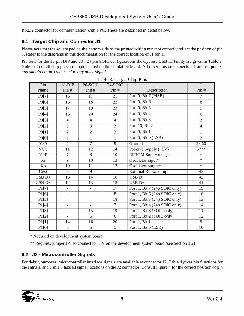
6.1. Target Chip and Connector J1Please note that the square pad on the bottom side of the printed wiring may not correctly reflect the position of pin1. Refer to the diagrams in this documentation for the correct location of J1 pin 1.
Pin-outs for the 18-pin DIP and 20 / 24-pin SOIC configurations the Cypress USB IC family are given in Table 3.Note that not all chip pins are implemented on the emulation board. All other pins on connector J1 are test points,and should not be connected to any other signal.
* Not used on development system board
** Requires jumper JP1 to connect to +5V on the development system board (see Section 3.2)
6.2. J2 - Microcontroller SignalsFor debug purposes, microcontroller interface signals are available at connector J2. Table 4 gives pin functions forthe signals, and Table 5 lists all signal locations on the J2 connector. Consult Figure 4 for the correct position of pin
Table 3: Target Chip PinsPin
Name18-DIPPin #
20-SOICPin #
24-SOICPin # Description
J1 Pin #
P0[7] 15 17 21 Port 0, Bit 7 (MSB) 7P0[6] 16 18 22 Port 0, Bit 6 8P0[5] 17 19 23 Port 0, Bit 5 5P0[4] 18 20 24 Port 0, Bit 4 6P0[3] 4 4 4 Port 0, Bit 3 3P0[2] 3 3 3 Port 10, Bit 2 4P0[1] 2 2 2 Port 0, Bit 1 1P0[0] 1 1 1 Port 0, Bit 0 (LSB) 2VSS 6 7 9 Ground 59,60VCC 11 12 14 Positive Supply (+5V) 57**VPP 7 8 10 EPROM Supervoltage* *Xi 9 10 12 Oscillator input* *Xo 10 11 13 Oscillator output* *
Cext 8 9 11 External RC wake-up 43 USB D+ 13 14 16 USB D+ 42USB D− 12 13 15 USB D− 41
P1[7] - - 17 Port 1, Bit 7 (24p SOIC only) 15P1[6] - - 8 Port 1, Bit 6 (24p SOIC only) 16P1[5] - - 18 Port 1, Bit 5 (24p SOIC only) 13P1[4] - - 7 Port 1, Bit 4 (24p SOIC only) 14P1[3] - 15 19 Port 1, Bit 3 (SOIC only) 11P1[2] - 6 6 Port 1, Bit 2 (SOIC only) 12P1[1] 14 16 20 Port 1, Bit 1 9P1[0] 5 5 5 Port 1, Bit 0 (LSB) 10

Ver 2.4 – 9 –
CY3650 USB Development System User’s Guide
1.Table 4: J2 Pin Descriptions
NAME FUNCTION
IA[12:0] 13-bit address bus for program memory
ID[7:0] 8-bit Instruction Data from program memory
IROMS_ Program ROM chip select (active low)
IRAMS_ Program RAM chip select (active low)
IRAMR_ Program RAM read enable (active low)
IRAMW_ Program RAM write enable (active low)
DB[7:0] 8-bit RAM Data bus
DA[7:0] 8-bit RAM Address bus
MR_ Memory read enable for data RAM (active low)
MW_ Memory write enable for data RAM (active low)
IOW_ I/O write enable (active low)
IOR_ I/O read enable (active low)
SOI Start of instruction - goes high at beginning of new instruction
TRQ Test Mode Request
IRQ Interrupt Request Signal
IRA Interrupt Acknowledge
BRA Bus Request Acknowledge
BRQ Bus Request - When high, data and address busses are driven externally
RESET Not used
MASTER RESET Reset signal for the board (active high)
CLOCK 12 MHz clock signal
VCC Connection to development board’s +5V
GND Ground

– 10 – Ver 2.4
CY3650 USB Development System User’s Guide
6.3. J3 - RS232 ConnectorJ3 is a 9-pin male connector for RS-232 interface to a host PC. Connections are shown in Table 6. Pins not listedare not connected
.
Table 5: J2 Connector Pin-out Pin # Description Pin # Description
1 IA0 2 IA13 IA2 4 IA35 IA4 6 IA57 IA6 8 IA79 IA8 10 IA9
11 IA10 12 IA1113 IA12 14 GND15 IRAMS_ 16 IRAMR_17 IRAMW_ 18 IOW_19 IOR_ 20 SOI21 - 22 BRQ23 IRQ 24 IRA25 BRA 26 TRQ27 RESET 28 MASTER RESET29 MR_ 30 MW_31 GND 32 ID033 ID1 34 ID235 ID3 36 ID437 ID5 38 ID639 ID7 40 IROMS_41 CLOCK 42 GND43 DB7 44 DB645 DB5 46 DB447 DB3 48 DB249 DB1 50 DB051 DA7 52 DA653 DA5 54 DA455 DA3 56 DA257 DA1 58 DA059 VCC 60 GND
Table 6: J3 RS-232 Connector Pin-outPin Function2 RXD - Output data to PC3 TXD - Input data from PC6 DSR - RUN_ signal to PC debug interface7 RTS - input from PC (not used)