CVD Synthetic Diamonds from Gemesis Corp. · PDF file80 CVD SYNTHETIC DIAMONDS FROM GEMESIS...
18
80 CVD SYNTHETIC DIAMONDS FROM GEMESIS CORP . GEMS & GEMOLOGY SUMMER 2012 A long with the conventional high-pressure, high-temperature (HPHT) growth technique, single-crystal synthetic diamond can be pro- duced using chemical vapor deposition (CVD). Tech- nological advances and a greater understanding of the crystal growth processes have led to significant im- provements in quality over the last decade. Today, CVD-grown faceted synthetic diamonds are present in the jewelry market in a variety of colors and sizes (e.g., Wang et al., 2003, 2005; Martineau et al., 2004). Furthermore, post-growth treatments to improve the color and transparency of these materials have been investigated. In November 2010 Gemesis Corp., a well-known manufacturer of gem-quality HPHT synthetic dia- monds, announced plans to market colorless and near-colorless CVD synthetics (Graff, 2010). Since March 2012, the company has sold mounted and loose CVD synthetic diamonds (e.g., figure 1). Because of the high cost and difficulty to manu- facture colorless HPHT synthetics, growth methods have traditionally focused on fancy colors. However, now it is colorless and near-colorless CVD synthet- ics, such as those developed by Gemesis, that pose the greatest commercial challenge to natural dia- monds (treated and untreated) of comparable quality. This study follows an initial report by Wang and Moses (2011) and presents gemological characteris- tics and spectroscopic features of new CVD synthet- ics from Gemesis. Key identification features that help separate these products from natural diamonds are also discussed. CVD Growth. While HPHT growth takes place under temperature and pressure conditions in which dia- mond is the stable phase of carbon, the CVD tech- nique enables growth under conditions where diamond is metastable with respect to graphite. This means that although diamond is kinetically stable, it is thermodynamically unstable. The technique is based on a gas-phase chemical reaction involving a hydrocarbon gas (such as methane) in an excess of hy- drogen gas occurring above a substrate. For single- crystal synthetic diamond growth the substrate is also a synthetic diamond, usually in the form of a {100}- oriented polished plate. Multiple substrates can be placed simultaneously in the CVD reaction chamber. CVD SYNTHETIC DIAMONDS FROM GEMESIS CORP . Wuyi Wang, Ulrika F. S. D’Haenens-Johansson, Paul Johnson, Kyaw Soe Moe, Erica Emerson, Mark E. Newton, and Thomas M. Moses FEATURE ARTICLES Gemological and spectroscopic properties of CVD synthetic diamonds from Gemesis Corp. were ex- amined. Their color (colorless, near-colorless, and faint, ranging from F to L) and clarity (typically VVS) grades were comparable to those of top natural diamonds, and their average weight was nearly 0.5 ct. Absorption spectra in the mid- and near-infrared regions were free from defect-related features, except for very weak absorption attributed to isolated nitrogen, but all samples were classified as type IIa. Vary- ing intensities of [Si-V] – and isolated nitrogen were detected with UV-Vis-NIR absorption spectroscopy. Electron paramagnetic resonance was used to quantify the neutral single substitutional nitrogen content. Photoluminescence spectra were dominated by N-V centers, [Si-V] – , H3, and many unassigned weak emissions. The combination of optical centers strongly suggests that post-growth treatments were applied to improve color and transparency. PL spectroscopy at low temperature and UV fluorescence imaging are critical in separating these synthetic products from their natural counterparts. See end of article for About the Authors and Acknowledgments. GEMS & GEMOLOGY , Vol. 48, No. 2, pp. 80–97, http://dx.doi.org/10.5741/GEMS.48.2.80. © 2012 Gemological Institute of America
Transcript of CVD Synthetic Diamonds from Gemesis Corp. · PDF file80 CVD SYNTHETIC DIAMONDS FROM GEMESIS...
80 CVD SYNTHETIC DIAMONDS FROM GEMESIS CORP. GEMS & GEMOLOGY SUMMER 2012
Along with the conventional high-pressure,high-temperature (HPHT) growth technique,single-crystal synthetic diamond can be pro-
duced using chemical vapor deposition (CVD). Tech-nological advances and a greater understanding of thecrystal growth processes have led to significant im-provements in quality over the last decade. Today,CVD-grown faceted synthetic diamonds are presentin the jewelry market in a variety of colors and sizes(e.g., Wang et al., 2003, 2005; Martineau et al., 2004).Furthermore, post-growth treatments to improve thecolor and transparency of these materials have beeninvestigated.
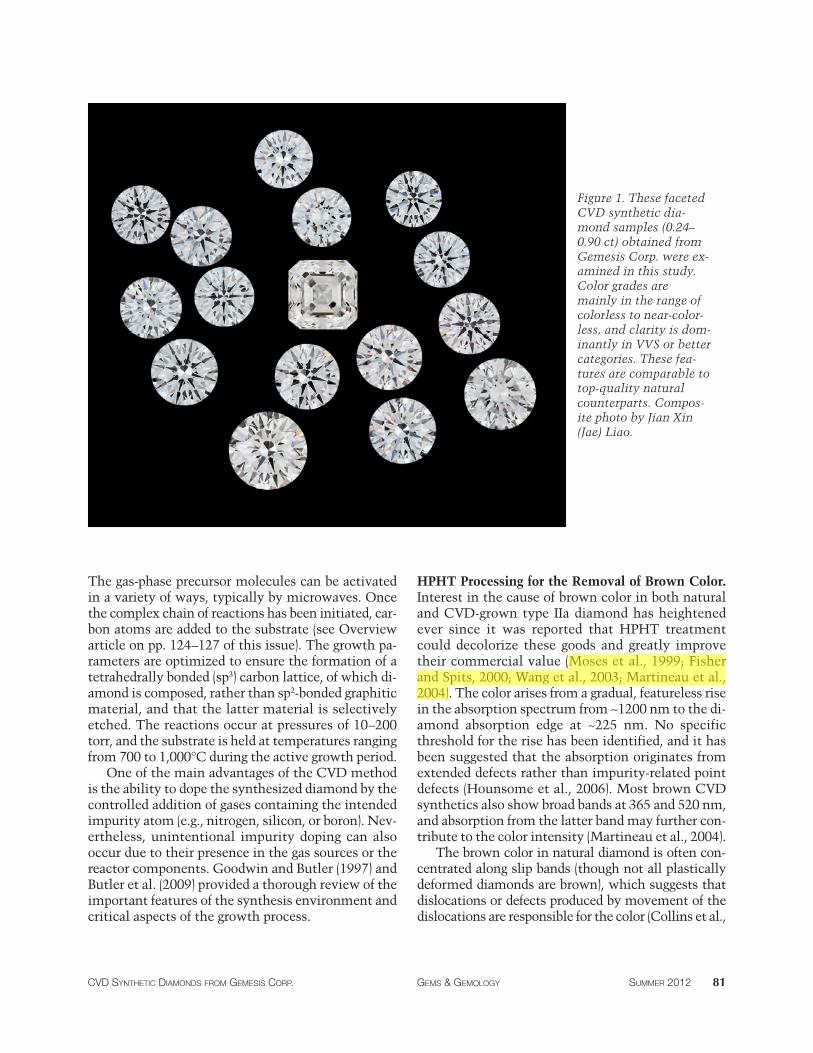
In November 2010 Gemesis Corp., a well-knownmanufacturer of gem-quality HPHT synthetic dia-monds, announced plans to market colorless andnear-colorless CVD synthetics (Graff, 2010). SinceMarch 2012, the company has sold mounted andloose CVD synthetic diamonds (e.g., figure 1).
Because of the high cost and difficulty to manu-facture colorless HPHT synthetics, growth methods
have traditionally focused on fancy colors. However,now it is colorless and near-colorless CVD synthet-ics, such as those developed by Gemesis, that posethe greatest commercial challenge to natural dia-monds (treated and untreated) of comparable quality.This study follows an initial report by Wang andMoses (2011) and presents gemological characteris-tics and spectroscopic features of new CVD synthet-ics from Gemesis. Key identification features thathelp separate these products from natural diamondsare also discussed.
CVD Growth.While HPHT growth takes place undertemperature and pressure conditions in which dia-mond is the stable phase of carbon, the CVD tech-nique enables growth under conditions wherediamond is metastable with respect to graphite. Thismeans that although diamond is kinetically stable, itis thermodynamically unstable. The technique isbased on a gas-phase chemical reaction involving ahydrocarbon gas (such as methane) in an excess of hy-drogen gas occurring above a substrate. For single-crystal synthetic diamond growth the substrate is alsoa synthetic diamond, usually in the form of a {100}-oriented polished plate. Multiple substrates can beplaced simultaneously in the CVD reaction chamber.
CVD SYNTHETIC DIAMONDS FROMGEMESIS CORP.Wuyi Wang, Ulrika F. S. D’Haenens-Johansson, Paul Johnson, Kyaw Soe Moe, Erica Emerson, Mark E. Newton, and Thomas M. Moses
FEATURE ARTICLES
Gemological and spectroscopic properties of CVD synthetic diamonds from Gemesis Corp. were ex-amined. Their color (colorless, near-colorless, and faint, ranging from F to L) and clarity (typically VVS)grades were comparable to those of top natural diamonds, and their average weight was nearly 0.5 ct.Absorption spectra in the mid- and near-infrared regions were free from defect-related features, exceptfor very weak absorption attributed to isolated nitrogen, but all samples were classified as type IIa. Vary-ing intensities of [Si-V]– and isolated nitrogen were detected with UV-Vis-NIR absorption spectroscopy.Electron paramagnetic resonance was used to quantify the neutral single substitutional nitrogen content.Photoluminescence spectra were dominated by N-V centers, [Si-V]–, H3, and many unassigned weakemissions. The combination of optical centers strongly suggests that post-growth treatments were appliedto improve color and transparency. PL spectroscopy at low temperature and UV fluorescence imagingare critical in separating these synthetic products from their natural counterparts.
See end of article for About the Authors and Acknowledgments.GEMS & GEMOLOGY, Vol. 48, No. 2, pp. 80–97,http://dx.doi.org/10.5741/GEMS.48.2.80.© 2012 Gemological Institute of America
Wang Summer 2012_Layout 1 6/18/12 7:47 AM Page 80
soverlin
Callout
Article title
soverlin
Callout
Author(s) byline
soverlin
Callout
Abstract: A summary and overview of the article.
soverlin
Callout
Introduction: Presents background/context and the objectives of the study.
soverlin
Highlight
soverlin
Callout
DOI: A permanent identifier for this article.
The gas-phase precursor molecules can be activatedin a variety of ways, typically by microwaves. Oncethe complex chain of reactions has been initiated, car-bon atoms are added to the substrate (see Overviewarticle on pp. 124–127 of this issue). The growth pa-rameters are optimized to ensure the formation of atetrahedrally bonded (sp3) carbon lattice, of which di -amond is composed, rather than sp2-bonded graphiticmaterial, and that the latter material is selectivelyetched. The reactions occur at pressures of 10–200torr, and the substrate is held at temperatures rangingfrom 700 to 1,000°C during the active growth period.
One of the main advantages of the CVD methodis the ability to dope the synthesized diamond by thecontrolled addition of gases containing the intendedimpurity atom (e.g., nitrogen, silicon, or boron). Nev-ertheless, unintentional impurity doping can alsooccur due to their presence in the gas sources or thereactor components. Goodwin and Butler (1997) andButler et al. (2009) provided a thorough review of theimportant features of the synthesis environment andcritical aspects of the growth process.
HPHT Processing for the Removal of Brown Color.Interest in the cause of brown color in both naturaland CVD-grown type IIa diamond has heightenedever since it was reported that HPHT treatmentcould decolorize these goods and greatly improvetheir commercial value (Moses et al., 1999; Fisherand Spits, 2000; Wang et al., 2003; Martineau et al.,2004). The color arises from a gradual, featureless risein the absorption spectrum from ~1200 nm to the di-amond absorption edge at ~225 nm. No specificthreshold for the rise has been identified, and it hasbeen suggested that the absorption originates fromextended defects rather than impurity-related pointdefects (Hounsome et al., 2006). Most brown CVDsynthetics also show broad bands at 365 and 520 nm,and absorption from the latter band may further con-tribute to the color intensity (Martineau et al., 2004).
The brown color in natural diamond is often con-centrated along slip bands (though not all plasticallydeformed diamonds are brown), which suggests thatdislocations or defects produced by movement of thedislocations are responsible for the color (Collins et al.,
CVD SYNTHETIC DIAMONDS FROM GEMESIS CORP. GEMS & GEMOLOGY SUMMER 2012 81
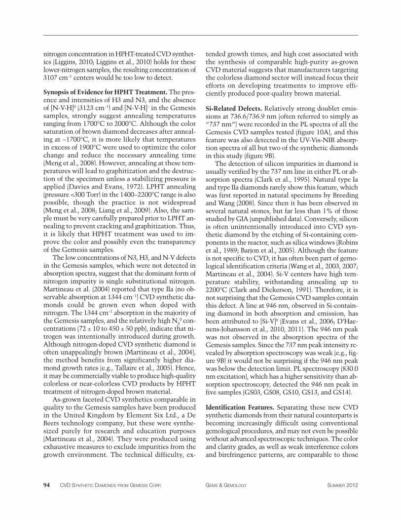
Figure 1. These facetedCVD synthetic dia-mond samples (0.24–0.90 ct) obtained fromGemesis Corp. were ex-amined in this study.Color grades aremainly in the range ofcolorless to near-color-less, and clarity is dom-inantly in VVS or bettercategories. These fea-tures are comparable totop-quality naturalcounterparts. Compos-ite photo by Jian Xin(Jae) Liao.
Wang Summer 2012_Layout 1 6/18/12 7:47 AM Page 81
soverlin
Callout
These are a few of the references listed at the end of the article.
soverlin
Highlight
soverlin
Callout
Figure captions offer a concise explanation of each illustration.
soverlin
Callout
G&G features large, full-color photos, photomicrographs, maps, charts, and other illustrations.
2000). However, analysis of the dislocation densities(~109/cm2) and their expected absorption strengths in-dicates that they alone cannot account for the ob-served color intensities (Fall et al., 2002; Willems etal., 2006; Mäki et al., 2007; Fisher et al., 2009). Otherstudies have proposed that the brown color is pro-duced by absorption from vacancy clusters or {111}-oriented vacancy discs also found in heavily distortedregions of the diamond lattice (Avalos and Dannefaer,2003; Hounsome et al., 2006; Bangert et al., 2009). Thepresence of clusters in brown natural diamond hasbeen confirmed by positron annihilation experiments,which demonstrated that the smaller clusters are op-tically active. These clusters have been shown to an-neal out and/or aggregate to form larger, opticallyinactive clusters at the HPHT annealing temperatures(up to ~2500°C) required to remove brown color fromnatural diamond (Avalos and Dannefaer, 2003; Fisheret al., 2009).
X-ray topography of brown single-crystal as-grown CVD synthetic diamond has not shown sig-nificant plastic deformation (Martineau et al., 2004).Dislocations in CVD material appear to have nucle-ated at the interface with the substrate, thus formingapproximately perpendicular to the growth surface(Martineau et al., 2004, 2009). The dislocation den-sities in as-grown CVD synthetic diamond are rela-tively low (~104–106/cm2) and thus are not consideredthe main cause of brown color. Positron annihilationstudies have shown that brown as-grown CVD syn-thetics may contain vacancy clusters of various sizes,ranging from monovacancies to nanometer-sizevoids (Mäki et al., 2007). The smaller clusters anneal
out in a temperature range (1400–1600°C) similar tothat at which the brown color is removed in CVDsynthetic diamond (Charles et al., 2004; Martineauet al., 2004; Mäki et al., 2007). Yet it has not beenconclusively demonstrated that these clusters are re-sponsible for coloration, especially as several otherpoint defects in CVD synthetic diamond are createdand destroyed at these temperatures. The differencein the temperature stability of color-causing defectsbetween natural and CVD synthetic brown diamondis not yet understood, and theoretical and experimen-tal studies are ongoing. Gem-quality CVD specimens with post-growth
treatments have occasionally been submitted to gemlaboratories for grading (Chadwick, 2008a,b). Thepurpose of the treatment is not limited to changingthe color from brown to colorless, as intense pinkCVD synthetic diamonds from Apollo (Wang et al.,2010) have also shown evidence of treatment withmultiple steps.
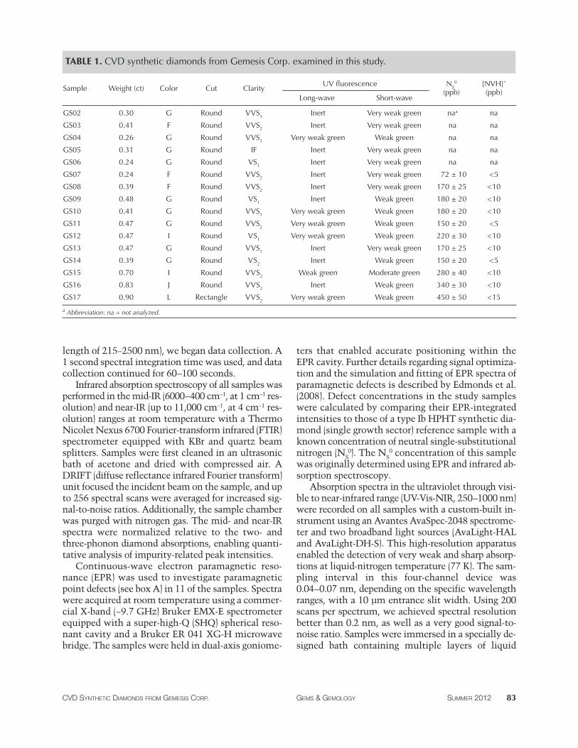
MATERIALS AND METHODSFor this investigation, we purchased 16 faceted CVDsynthetic diamonds from Gemesis (table 1; see alsofigure 1). These ranged from 0.24 to 0.90 ct, with anaverage weight of 0.46 ct. The majority (94%) werecut as round brilliants, with depths of 2.41 to 3.69mm, averaging 2.93 mm. These CVD synthetics arerepresentative of the current production being soldon the Gemesis website.
Experienced members of GIA’s diamond gradingstaff determined color and clarity grades using GIA’sgrading system. Internal features were examinedwith a standard gemological binocular microscopeand a research-grade Nikon microscope, using a va-riety of lighting techniques, including darkfield andfiber-optic illumination and polarization. Reactionsto UV radiation were tested in a darkened room witha conventional 4 watt combination long-wave (365nm) and short-wave (254 nm) UV lamp. We also ex-amined the samples for fluorescence, phosphores-cence, and crystal growth characteristics using theDiamond Trading Company (DTC) DiamondViewinstrument (Welbourn et al., 1996). Phosphorescenceimages were collected with a 0.1 second delay and 5seconds of exposure time.Phosphorescence spectra were collected on all
samples at room temperature with an Ocean OpticsHR4000 spectrometer. After illuminating the sam-ples for 30 seconds with an Avantes AvaLight-DH-Sdeuterium-halogen light source (emission wave-
82 CVD SYNTHETIC DIAMONDS FROM GEMESIS CORP. GEMS & GEMOLOGY SUMMER 2012
In Brief• Gemesis Corp. has sold mounted and loose CVD syn- thetic diamonds since March 2012.
• The latest generation products examined for this report ranged up to 0.90 ct, and most were near-colorless and had clarity grades between IF and VVS; all but one were round brilliants.
• Spectroscopic evidence indicates a likelihood that these CVD synthetics have undergone post-growth HPHT processing to enhance their color and possibly their clarity.
• This material is conclusively identified by PL spec- troscopy and DiamondView fluorescence images.
Wang Summer 2012_Layout 1 6/18/12 7:47 AM Page 82
soverlin
Text Box
In Brief: A list of key takeaways from the article.
soverlin
Callout
Materials and Methods: Detailed descriptions of the samples studied and the techniques used to characterize them.
length of 215–2500 nm), we began data collection. A1 second spectral integration time was used, and datacollection continued for 60–100 seconds.Infrared absorption spectroscopy of all samples was
performed in the mid-IR (6000–400 cm−1, at 1 cm−1 res-olution) and near-IR (up to 11,000 cm−1, at 4 cm−1 res-olution) ranges at room temperature with a ThermoNicolet Nexus 6700 Fourier-transform infrared (FTIR)spectrometer equipped with KBr and quartz beamsplitters. Samples were first cleaned in an ultrasonicbath of acetone and dried with compressed air. ADRIFT (diffuse reflectance infrared Fourier transform)unit focused the incident beam on the sample, and upto 256 spectral scans were averaged for increased sig-nal-to-noise ratios. Additionally, the sample chamberwas purged with nitrogen gas. The mid- and near-IRspectra were normalized relative to the two- andthree-phonon diamond absorptions, enabling quanti-tative analysis of impurity-related peak intensities.Continuous-wave electron paramagnetic reso-
nance (EPR) was used to investigate paramagneticpoint defects (see box A) in 11 of the samples. Spectrawere acquired at room temperature using a commer-cial X-band (~9.7 GHz) Bruker EMX-E spectrometerequipped with a super-high-Q (SHQ) spherical reso-nant cavity and a Bruker ER 041 XG-H microwavebridge. The samples were held in dual-axis goniome-
ters that enabled accurate positioning within theEPR cavity. Further details regarding signal optimiza-tion and the simulation and fitting of EPR spectra ofparamagnetic defects is described by Edmonds et al.(2008). Defect concentrations in the study sampleswere calculated by comparing their EPR-integratedintensities to those of a type Ib HPHT synthetic dia-mond (single growth sector) reference sample with aknown concentration of neutral single-substitutionalnitrogen (NS
0). The NS0 concentration of this sample
was originally determined using EPR and infrared ab-sorption spectroscopy. Absorption spectra in the ultraviolet through visi-
ble to near-infrared range (UV-Vis-NIR, 250–1000 nm)were recorded on all samples with a custom-built in-strument using an Avantes AvaSpec-2048 spectrome-ter and two broadband light sources (AvaLight-HALand AvaLight-DH-S). This high-resolution apparatusenabled the detection of very weak and sharp absorp-tions at liquid-nitrogen temperature (77 K). The sam-pling interval in this four-channel device was0.04–0.07 nm, depending on the specific wavelengthranges, with a 10 µm entrance slit width. Using 200scans per spectrum, we achieved spectral resolutionbetter than 0.2 nm, as well as a very good signal-to-noise ratio. Samples were immersed in a specially de-signed bath containing multiple layers of liquid
CVD SYNTHETIC DIAMONDS FROM GEMESIS CORP. GEMS & GEMOLOGY SUMMER 2012 83
UV fluorescence NS0 [NVH]-
Long-wave Short-wave(ppb) (ppb)
GS02 0.30 G Round VVS1 Inert Very weak green naa na
GS03 0.41 F Round VVS2 Inert Very weak green na na
GS04 0.26 G Round VVS1 Very weak green Weak green na na
GS05 0.31 G Round IF Inert Very weak green na na
GS06 0.24 G Round VS1 Inert Very weak green na na
GS07 0.24 F Round VVS2 Inert Very weak green 72 ± 10 <5
GS08 0.39 F Round VVS2 Inert Very weak green 170 ± 25 <10
GS09 0.48 G Round VS1 Inert Weak green 180 ± 20 <10
GS10 0.41 G Round VVS1 Very weak green Weak green 180 ± 20 <10
GS11 0.47 G Round VVS2 Very weak green Weak green 150 ± 20 <5
GS12 0.47 I Round VS1 Very weak green Weak green 220 ± 30 <10
GS13 0.47 G Round VVS1 Inert Very weak green 170 ± 25 <10
GS14 0.39 G Round VS2 Inert Weak green 150 ± 20 <5
GS15 0.70 I Round VVS2 Weak green Moderate green 280 ± 40 <10
GS16 0.83 J Round VVS2 Inert Weak green 340 ± 30 <10
GS17 0.90 L Rectangle VVS2 Very weak green Weak green 450 ± 50 <15
TABLE 1. CVD synthetic diamonds from Gemesis Corp. examined in this study.
a Abbreviation: na = not analyzed.
Sample Weight (ct) Color Cut Clarity
Wang Summer 2012_Layout 1 6/18/12 7:47 AM Page 83
soverlin
Text Box
Tables present large amounts of data in a limited space.
nitrogen (patent pending), ensuring consistent temper-ature and a stable environment free of nitrogen gasbubbles.
A commercial Renishaw InVia Raman confocal mi-crospectrometer, equipped with the liquid nitrogenbath setup used for UV-Vis-NIR spectroscopy, was usedfor low-temperature photoluminescence (PL) spectralanalysis of all samples. Various defect centers were ex-cited using five excitation wavelengths produced by
four laser systems. An Ar-ion laser was operated at ex-citation wavelengths of 488.0 nm (for the 490–850 nmrange) and 514.5 nm (for the 517–850 nm range). PLspectra were collected in the 640–850 nm range usingan He-Ne laser (632.8 nm), and in the 835–1000 nmrange using a diode laser (830.0 nm). In addition, an He-Cd metal-vapor laser (324.8 nm) was used for the 370–800 nm range. Up to three scans were accumulated foreach spectrum to improve the signal-to-noise ratio.
84 CVD SYNTHETIC DIAMONDS FROM GEMESIS CORP. GEMS & GEMOLOGY SUMMER 2012
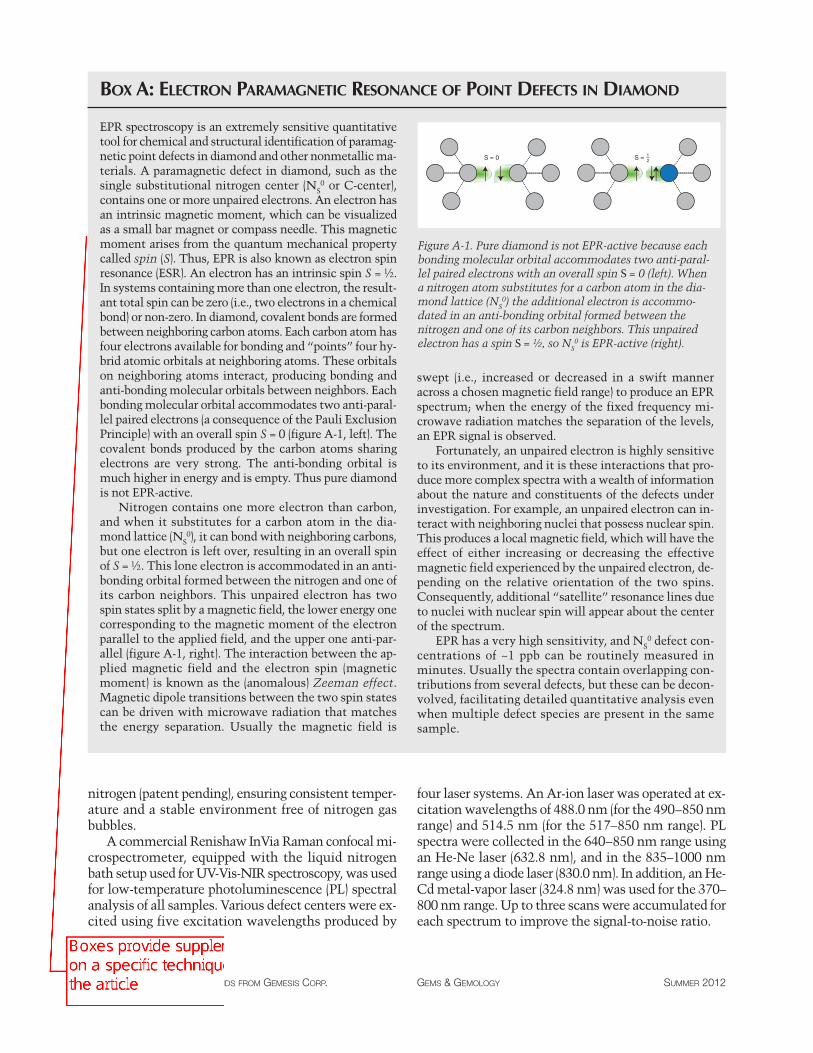
EPR spectroscopy is an extremely sensitive quantitativetool for chemical and structural identification of paramag-netic point defects in diamond and other nonmetallic ma-terials. A paramagnetic defect in diamond, such as thesingle substitutional nitrogen center (NS
0 or C-center),contains one or more unpaired electrons. An electron hasan intrinsic magnetic moment, which can be visualizedas a small bar magnet or compass needle. This magneticmoment arises from the quantum mechanical propertycalled spin (S). Thus, EPR is also known as electron spinresonance (ESR). An electron has an intrinsic spin S = ½.In systems containing more than one electron, the result-ant total spin can be zero (i.e., two electrons in a chemicalbond) or non-zero. In diamond, covalent bonds are formedbetween neighboring carbon atoms. Each carbon atom hasfour electrons available for bonding and “points” four hy-brid atomic orbitals at neighboring atoms. These orbitalson neighboring atoms interact, producing bonding andanti-bonding molecular orbitals between neighbors. Eachbonding molecular orbital accommodates two anti-paral-lel paired electrons (a consequence of the Pauli ExclusionPrinciple) with an overall spin S = 0 (figure A-1, left). Thecovalent bonds produced by the carbon atoms sharingelectrons are very strong. The anti-bonding orbital ismuch higher in energy and is empty. Thus pure diamondis not EPR-active.
Nitrogen contains one more electron than carbon,and when it substitutes for a carbon atom in the dia-mond lattice (NS
0), it can bond with neighboring carbons,but one electron is left over, resulting in an overall spinof S = ½. This lone electron is accommodated in an anti-bonding orbital formed between the nitrogen and one ofits carbon neighbors. This unpaired electron has twospin states split by a magnetic field, the lower energy onecorresponding to the magnetic moment of the electronparallel to the applied field, and the upper one anti-par-allel (figure A-1, right). The interaction between the ap-plied magnetic field and the electron spin (magneticmoment) is known as the (anomalous) Zeeman effect.Magnetic dipole transitions between the two spin statescan be driven with microwave radiation that matchesthe energy separation. Usually the magnetic field is
swept (i.e., increased or decreased in a swift manneracross a chosen magnetic field range) to produce an EPRspectrum; when the energy of the fixed frequency mi-crowave radiation matches the separation of the levels,an EPR signal is observed.
Fortunately, an unpaired electron is highly sensitiveto its environment, and it is these interactions that pro-duce more complex spectra with a wealth of informationabout the nature and constituents of the defects underinvestigation. For example, an unpaired electron can in-teract with neighboring nuclei that possess nuclear spin.This produces a local magnetic field, which will have theeffect of either increasing or decreasing the effectivemagnetic field experienced by the unpaired electron, de-pending on the relative orientation of the two spins.Consequently, additional “satellite” resonance lines dueto nuclei with nuclear spin will appear about the centerof the spectrum.
EPR has a very high sensitivity, and NS0 defect con-
centrations of ~1 ppb can be routinely measured inminutes. Usually the spectra contain overlapping con -tri butions from several defects, but these can be decon-volved, facilitating detailed quantitative analysis evenwhen multiple defect species are present in the samesample.
BOX A: ELECTRON PARAMAGNETIC RESONANCE OF POINT DEFECTS IN DIAMOND
Figure A-1. Pure diamond is not EPR-active because eachbonding molecular orbital accommodates two anti-paral-lel paired electrons with an overall spin S = 0 (left). Whena nitrogen atom substitutes for a carbon atom in the dia-mond lattice (NS
0) the additional electron is accommo-dated in an anti-bonding orbital formed between thenitrogen and one of its carbon neighbors. This unpairedelectron has a spin S = ½, so NS
0 is EPR-active (right).
S = 0 S = 12
Wang Summer 2012_Layout 1 6/18/12 7:47 AM Page 84
soverlin
Callout
Boxes provide supplementary information on a specific technique or other topic from the article
RESULTS Color and Shape. Three of the 16 samples weregraded as colorless (F color) and 12 as near-colorless(G–J; see table 1). Only one was faintly colored (L),with the color falling within the yellow hue range.The three largest diamonds had the poorest colorgrades. The largest sample (0.90 ct) was the only onepolished into a rectangular shape; the other 15 sam-ples were round brilliants.
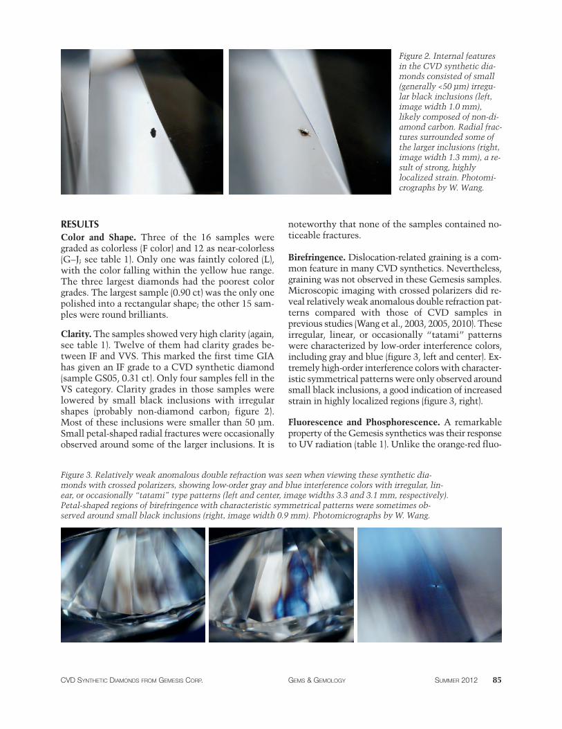
Clarity.The samples showed very high clarity (again,see table 1). Twelve of them had clarity grades be-tween IF and VVS. This marked the first time GIAhas given an IF grade to a CVD synthetic diamond(sample GS05, 0.31 ct). Only four samples fell in theVS category. Clarity grades in those samples werelowered by small black inclusions with irregularshapes (probably non-diamond carbon; figure 2).Most of these inclusions were smaller than 50 µm.Small petal-shaped radial fractures were occasionallyobserved around some of the larger inclusions. It is
noteworthy that none of the samples contained no-ticeable fractures.
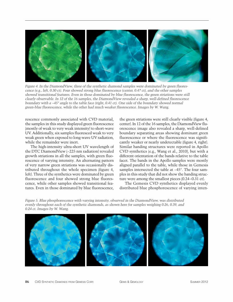
Birefringence. Dislocation-related graining is a com-mon feature in many CVD synthetics. Nevertheless,graining was not observed in these Gemesis samples.Microscopic imaging with crossed polarizers did re-veal relatively weak anomalous double refraction pat-terns compared with those of CVD samples inprevious studies (Wang et al., 2003, 2005, 2010). Theseirregular, linear, or occasionally “tatami” patternswere characterized by low-order interference colors,including gray and blue (figure 3, left and center). Ex-tremely high-order interference colors with character-istic symmetrical patterns were only observed aroundsmall black inclusions, a good indication of increasedstrain in highly localized regions (figure 3, right).
Fluorescence and Phosphorescence. A remarkableproperty of the Gemesis synthetics was their responseto UV radiation (table 1). Unlike the orange-red fluo-
CVD SYNTHETIC DIAMONDS FROM GEMESIS CORP. GEMS & GEMOLOGY SUMMER 2012 85
Figure 3. Relatively weak anomalous double refraction was seen when viewing these synthetic dia-monds with crossed polarizers, showing low-order gray and blue interference colors with irregular, lin-ear, or occasionally “tatami” type patterns (left and center, image widths 3.3 and 3.1 mm, respectively).Petal-shaped regions of birefringence with characteristic symmetrical patterns were sometimes ob-served around small black inclusions (right, image width 0.9 mm). Photomicrographs by W. Wang.
Figure 2. Internal featuresin the CVD synthetic dia-monds consisted of small(generally <50 μm) irregu-lar black inclusions (left,image width 1.0 mm),likely composed of non-di-amond carbon. Radial frac-tures surrounded some ofthe larger inclusions (right,image width 1.3 mm), a re-sult of strong, highly localized strain. Photomi-crographs by W. Wang.
Wang Summer 2012_Layout 1 6/18/12 7:47 AM Page 85
soverlin
Callout
Results: Description of the samples' optical and physical properties, microscopic observations, chemical composition analysis, and other experimental data.
soverlin
Callout
Photomicrographs reveal the important internal features of a gemstone
rescence commonly associated with CVD material,the samples in this study displayed green fluorescence(mostly of weak to very weak intensity) to short-waveUV. Additionally, six samples fluoresced weak to veryweak green when exposed to long-wave UV radiation,while the remainder were inert.
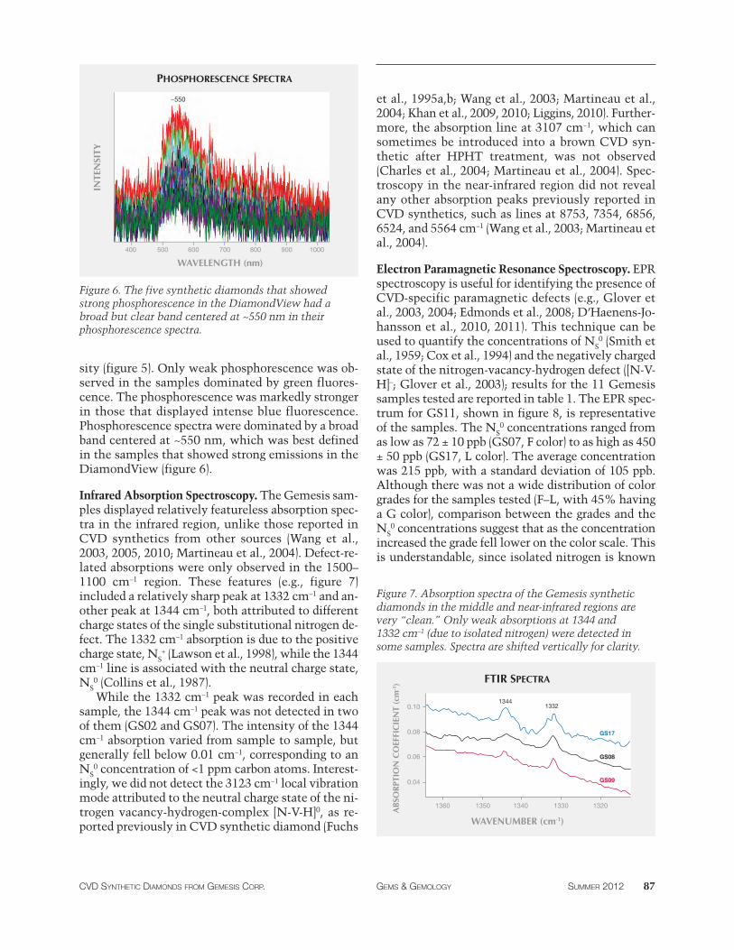
The high-intensity ultra-short UV wavelength ofthe DTC DiamondView (~225 nm radiation) revealedgrowth striations in all the samples, with green fluo-rescence of varying intensity. An alternating patternof very narrow green striations was occasionally dis-tributed throughout the whole specimen (figure 4,left). Three of the synthetics were dominated by greenfluorescence and four showed strong blue fluores-cence, while other samples showed transitional fea-tures. Even in those dominated by blue fluorescence,
the green striations were still clearly visible (figure 4,center). In 12 of the 16 samples, the DiamondView flu-orescence image also revealed a sharp, well-definedboundary separating areas showing dominant greenfluorescence or where the fluorescence was signifi-cantly weaker or nearly undetectable (figure 4, right).Similar banding structures were reported in ApolloCVD synthetics (e.g., Wang et al., 2010), but with adifferent orientation of the bands relative to the tablefacet. The bands in the Apollo samples were mostlyaligned parallel to the table, while those in Gemesissamples intersected the table at ~45°. The four sam-ples in this study that did not show the banding struc-ture were among the smallest pieces (0.24–0.31 ct).
The Gemesis CVD synthetics displayed evenlydistributed blue phosphorescence of varying inten-
86 CVD SYNTHETIC DIAMONDS FROM GEMESIS CORP. GEMS & GEMOLOGY SUMMER 2012
Figure 5. Blue phosphorescence with varying intensity, observed in the DiamondView, was distributedevenly throughout each of the synthetic diamonds, as shown here for samples weighing 0.26, 0.39, and0.24 ct. Images by W. Wang.
Figure 4. In the DiamondView, three of the synthetic diamond samples were dominated by green fluores-cence (e.g., left, 0.30 ct). Four showed strong blue fluorescence (center, 0.47 ct), and the other samplesshowed transitional features. Even in those dominated by blue fluorescence, the green striations were stillclearly observable. In 12 of the 16 samples, the DiamondView revealed a sharp, well-defined fluorescenceboundary with a ~45° angle to the table face (right, 0.41 ct). One side of the boundary showed normalgreen-blue fluorescence, while the other had much weaker fluorescence. Images by W. Wang.
Wang Summer 2012_Layout 1 6/18/12 7:47 AM Page 86
sity (figure 5). Only weak phosphorescence was ob-served in the samples dominated by green fluores-cence. The phosphorescence was markedly strongerin those that displayed intense blue fluorescence.Phosphorescence spectra were dominated by a broadband centered at ~550 nm, which was best definedin the samples that showed strong emissions in theDiamondView (figure 6).
Infrared Absorption Spectroscopy.The Gemesis sam-ples displayed relatively featureless absorption spec-tra in the infrared region, unlike those reported inCVD synthetics from other sources (Wang et al.,2003, 2005, 2010; Martineau et al., 2004). Defect-re-lated absorptions were only observed in the 1500–1100 cm–1 region. These features (e.g., figure 7)included a relatively sharp peak at 1332 cm−1 and an-other peak at 1344 cm−1, both attributed to differentcharge states of the single substitutional nitrogen de-fect. The 1332 cm−1 absorption is due to the positivecharge state, NS
+ (Lawson et al., 1998), while the 1344cm−1 line is associated with the neutral charge state,NS
0 (Collins et al., 1987). While the 1332 cm−1 peak was recorded in each
sample, the 1344 cm−1 peak was not detected in twoof them (GS02 and GS07). The intensity of the 1344cm−1 absorption varied from sample to sample, butgenerally fell below 0.01 cm−1, corresponding to anN S
0 concentration of <1 ppm carbon atoms. Interest-ingly, we did not detect the 3123 cm−1 local vibrationmode attributed to the neutral charge state of the ni-trogen vacancy-hydrogen-complex [N-V-H]0, as re-ported previously in CVD synthetic diamond (Fuchs
et al., 1995a,b; Wang et al., 2003; Martineau et al.,2004; Khan et al., 2009, 2010; Liggins, 2010). Further-more, the absorption line at 3107 cm−1, which cansometimes be introduced into a brown CVD syn-thetic after HPHT treatment, was not observed(Charles et al., 2004; Martineau et al., 2004). Spec-troscopy in the near-infrared region did not revealany other absorption peaks previously reported inCVD synthetics, such as lines at 8753, 7354, 6856,6524, and 5564 cm−1 (Wang et al., 2003; Martineau etal., 2004).
Electron Paramagnetic Resonance Spectroscopy. EPRspectroscopy is useful for identifying the presence ofCVD-specific paramagnetic defects (e.g., Glover etal., 2003, 2004; Edmonds et al., 2008; D’Haenens-Jo-hansson et al., 2010, 2011). This technique can beused to quantify the concentrations of NS
0 (Smith etal., 1959; Cox et al., 1994) and the negatively chargedstate of the nitrogen-vacancy-hydrogen defect ([N-V-H]–; Glover et al., 2003); results for the 11 Gemesissamples tested are reported in table 1. The EPR spec-trum for GS11, shown in figure 8, is representativeof the samples. The NS
0 concentrations ranged fromas low as 72 ± 10 ppb (GS07, F color) to as high as 450± 50 ppb (GS17, L color). The average concentrationwas 215 ppb, with a standard deviation of 105 ppb.Although there was not a wide distribution of colorgrades for the samples tested (F–L, with 45% havinga G color), comparison between the grades and theNS
0 concentrations suggest that as the concentrationincreased the grade fell lower on the color scale. Thisis understandable, since isolated nitrogen is known
CVD SYNTHETIC DIAMONDS FROM GEMESIS CORP. GEMS & GEMOLOGY SUMMER 2012 87
Figure 6. The five synthetic diamonds that showedstrong phosphorescence in the DiamondView had abroad but clear band centered at ~550 nm in theirphosphorescence spectra.
WAVELENGTH (nm)
INTE
NSI
TY
400 1000
PHOSPHORESCENCE SPECTRA
500 600 700 800 900
~550
Figure 7. Absorption spectra of the Gemesis syntheticdiamonds in the middle and near-infrared regions arevery “clean.” Only weak absorptions at 1344 and1332 cm–1 (due to isolated nitrogen) were detected insome samples. Spectra are shifted vertically for clarity.
WAVENUMBER (cm-1)
AB
SOR
PTIO
N C
OEF
FIC
IEN
T (c
m-1)
0.10
0.08
0.06
0.04
1360 1350 1340 1330 1320
13441332
GS17
GS08
GS09
FTIR SPECTRA
Wang Summer 2012_Layout 1 6/18/12 7:47 AM Page 87
soverlin
Callout
G&G articles deal with a variety of spectroscopic and other analytical techniques
to impart yellow color in diamond. The [N-V-H]– cen-ter was not detected by EPR, with upper concentra-tion limits ranging from 5 to 15 ppb (table 1).
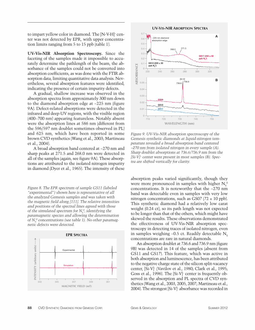
UV-Vis-NIR Absorption Spectroscopy. Since thefaceting of the samples made it impossible to accu-rately determine the pathlength of the beam, the ab-sorbance of the samples could not be converted intoabsorption coefficients, as was done with the FTIR ab-sorption data, limiting quantitative data analysis. Nev-ertheless, several absorption features were identified,indicating the presence of certain impurity defects.
A gradual, shallow increase was observed in theabsorption spectra from approximately 300 nm downto the diamond absorption edge at ~225 nm (figure9A). Defect-related absorptions were detected in theinfrared and deep-UV regions, with the visible region(400–700 nm) appearing featureless. Notably absentwere the absorption lines at 586 nm (different fromthe 596/597 nm doublet sometimes observed in PL)and 625 nm, which have been reported in somebrown CVD synthetics (Wang et al., 2003; Martineauet al., 2004).
A broad absorption band centered at ~270 nm andsharp peaks at 271.5 and 268.0 nm were detected inall of the samples (again, see figure 9A). These absorp-tions are attributed to the isolated nitrogen impurityin diamond (Dyer et al., 1965). The intensity of these
absorption peaks varied significantly, though theywere more pronounced in samples with higher NS
0
concentrations. It is noteworthy that the ~270 nmband was detectable even in samples with very lownitrogen concentrations, such as GS07 (72 ± 10 ppb).This synthetic diamond had a relatively low caratweight (0.24 ct), so its path length was not expectedto be longer than that of the others, which might haveskewed the results. These observations demonstratedthe effectiveness of UV-Vis-NIR absorption spec-troscopy in detecting traces of isolated nitrogen, evenin samples weighing ~0.5 ct. Readily detectable NSconcentrations are rare in natural diamonds.
An absorption doublet at 736.6 and 736.9 nm (figure9B) was detected in 14 of the samples (absent fromGS11 and GS17). This feature, which was active inboth absorption and luminescence, has been attributedto the negative charge state of the silicon split-vacancycenter, [Si-V]– (Vavilov et al., 1980; Clark et al., 1995;Goss et al., 1996). The [Si-V]– center is frequently ob-served in the absorption and PL spectra of CVD syn-thetics (Wang et al., 2003, 2005, 2007; Martineau et al.,2004). The strongest [Si-V]– absorbance was recorded in
88 CVD SYNTHETIC DIAMONDS FROM GEMESIS CORP. GEMS & GEMOLOGY SUMMER 2012
Figure 9. UV-Vis-NIR absorption spectroscopy of theGemesis synthetic diamonds at liquid-nitrogen tem-perature revealed a broad absorption band centered~270 nm from isolated nitrogen in every sample (A).Sharp doublet absorptions at 736.6/736.9 nm from the[Si-V]– center were present in most samples (B). Spec-tra are shifted vertically for clarity.
WAVELENGTH (nm)
AB
SOR
BAN
CE
0.7
220 240 260 280 300
UV-VIS-NIR ABORPTION SPECTRA
320
0.6
0.5
0.4
0.3
0.2
0.1
0
GS17 (450 ± 50 ppb NS
0)
GS12 (220 ± 30 ppb NS
0)
~225 nm diamond absorption edge
0.05
0.04
0.03
0.02
0.01
0
715 725 735 755745
GS09
GS10
GS11
736.6736.9
[Si-V]–
A
B
268.0 271.5
Figure 8. The EPR spectrum of sample GS11 (labeled“experimental”) shown here is representative of allthe analyzed Gemesis samples and was taken withthe magnetic field along [111]. The relative intensitiesand positions of the spectral lines agreed with thoseof the simulated spectrum for NS
0, identifying theparamagnetic species and allowing the determinationof NS
0 concentrations (see table 1). No other paramag-netic defects were detected.
MAGNETIC FIELD (mT)
INTE
NSI
TY (
arbi
trar
y un
its)
343 345 347 349 351
EPR SPECTRA
Experimental
Simulation
Wang Summer 2012_Layout 1 6/18/12 7:47 AM Page 88
samples GS03, GS08, GS09, and GS14. Even so, therewas no clear correlation between diamond color gradesand concentrations of Si-related defects.
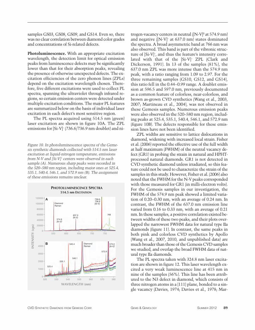
Photoluminescence. With an appropriate excitationwavelength, the detection limit for optical emissionpeaks from luminescence defects may be significantlylower than that for their absorption peaks, revealingthe presence of otherwise unexpected defects. The ex-citation efficiencies of the zero phonon lines (ZPLs)depend on the excitation wavelength chosen. There-fore, five different excitations were used to collect PLspectra, spanning the ultraviolet through infrared re-gions, so certain emission centers were detected undermultiple excitation conditions. The major PL featuresare summarized below on the basis of individual laserexcitation in each defect’s most sensitive region.
The PL spectra acquired using 514.5 nm (green)laser excitation are shown in figure 10A. The ZPLemissions for [Si-V]– (736.6/736.9 nm doublet) and ni-
trogen-vacancy centers in neutral ([N-V]0 at 574.9 nm)and negative ([N-V]– at 637.0 nm) states dominatedthe spectra. A broad asymmetric band at 766 nm wasalso observed. This band is part of the vibronic struc-ture of [Si-V]–, and thus the feature’s intensity corre-lated with that of the [Si-V]– ZPL (Clark andDicker son, 1991). In 13 of the samples (81%), the637.0 nm ZPL was more intense than the 574.9 nmpeak, with a ratio ranging from 1.09 to 2.97. For thethree remaining samples (GS10, GS12, and GS14),this ratio fell in the 0.44–0.99 range. A doublet emis-sion at 596.5 and 597.0 nm, previously documentedas a common feature of colorless, near-colorless, andbrown as-grown CVD synthetics (Wang et al., 2003,2007; Martineau et al., 2004), was not observed inthese Gemesis samples. Numerous emission peakswere also observed in the 520–580 nm region, includ-ing peaks at 525.4, 535.1, 540.4, 546.1, and 572.9 nm(figure 10B). The defects responsible for these emis-sion lines have not been identified.
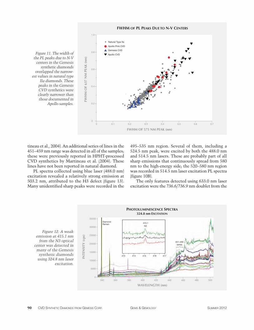
ZPL widths are sensitive to lattice dislocations indiamond, widening with increased local strain. Fisheret al. (2006) reported the effective use of the full widthat half maximum (FWHM) of the neutral vacancy de-fect (GR1) in probing the strain in natural and HPHT-processed natural diamonds. GR1 is not detected inCVD synthetic diamond unless irradiated, so this fea-ture could not be used to characterize the strain of thesamples in this study. However, Fisher et al. (2006) alsonoted that the FWHM for the N-V peaks correspondedwith those measured for GR1 (in milli-electron volts).For the Gemesis samples in our inves ti gation, theFWHM of the 574.9 nm peak showed a limited varia-tion of 0.20–0.30 nm, with an average of 0.24 nm. Incontrast, the FWHM of the 637.0 nm emission linevaried from 0.16 to 0.33 nm, with an average of 0.21nm. In these samples, a positive correlation existed be-tween widths of these two peaks, and their plots over-lapped the narrowest FWHM data for natural type IIadiamonds (figure 11). In contrast, the same peaks inboth pink and colorless CVD synthetics by Apollo(Wang et al., 2007, 2010, and unpublished data) aremuch broader than those of the Gemesis CVD sampleswe studied, and overlap the broad FWHM data of nat-ural type IIa diamonds.
The PL spectra taken with 324.8 nm laser excita-tion are shown in figure 12. This laser wavelength ex-cited a very weak luminescence line at 415 nm innine of the samples (56%). This line has been attrib-uted to the N3 defect in diamond, which consists ofthree nitrogen atoms in a {111} plane, bonded to a sin-gle vacancy (Davies, 1974; Davies et al., 1978; Mar-
CVD SYNTHETIC DIAMONDS FROM GEMESIS CORP. GEMS & GEMOLOGY SUMMER 2012 89
Figure 10. In photoluminescence spectra of the Geme-sis synthetic diamonds collected with 514.5 nm laserexcitation at liquid-nitrogen temperature, emissionsfrom N-V and [Si-V]– centers were observed in eachsample (A). Numerous sharp peaks were recorded inthe 520–580 nm region, including major ones at 525.4,535.1, 540.4, 546.1, and 572.9 nm (B). The assignmentof these emissions remains unclear.
WAVELENGTH (nm)
INTE
NSI
TY (
cps)
550 600 650 700 750
574.9
766
PHOTOLUMINESCENCE SPECTRA
120000
100000
80000
60000
40000
20000
0
[N-V]0
637.0[N-V]–
736.9[Si-V]–
736.6,
4000
3000
2000
1000
0520 530 540 550 560 570 580
575.0[N-V]0
572.9
546.1
540.4
535.1
525.4
A
B DiamondRaman
514.5 nm EXCITATION
DiamondRaman
Wang Summer 2012_Layout 1 6/18/12 7:47 AM Page 89
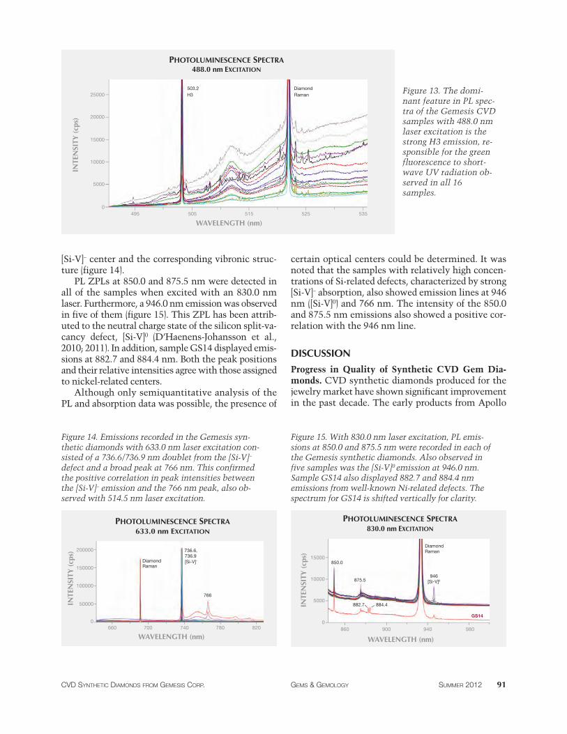
tineau et al., 2004). An additional series of lines in the451–459 nm range was detected in all of the samples;these were previously reported in HPHT-processedCVD synthetics by Martineau et al. (2004). Theselines have not been reported in natural diamond.
PL spectra collected using blue laser (488.0 nm)excitation revealed a relatively strong emission at503.2 nm, attributed to the H3 defect (figure 13).Many unidentified sharp peaks were recorded in the
495–535 nm region. Several of them, including a524.5 nm peak, were excited by both the 488.0 nmand 514.5 nm lasers. These are probably part of allsharp emissions that continuously spread from 580nm to the high-energy side; the 520–580 nm regionwas recorded in 514.5 nm laser excitation PL spectra(figure 10B).
The only features detected using 633.0 nm laserexcitation were the 736.6/736.9 nm doublet from the
90 CVD SYNTHETIC DIAMONDS FROM GEMESIS CORP. GEMS & GEMOLOGY SUMMER 2012
FWHM OF 575 NM PEAK (nm)
FWHM OF PL PEAKS DUE TO N-V CENTERS
0
Natural Type IIa
FWH
M O
F 63
7 N
M P
EAK
(nm
)
0.1 0.2 0.3 0.4 0.5 0.6 0.7
0.2
0.4
0.6
0.8
1.0
Apollo Pink CVD
Gemesis CVD
Apollo CVD
0
Figure 11. The width ofthe PL peaks due to N-Vcenters in the Gemesis
synthetic diamondsoverlapped the narrow-
est values in natural typeIIa diamonds. Thesepeaks in the GemesisCVD synthetics wereclearly narrower thanthose documented in
Apollo samples.
WAVELENGTH (nm)
INTE
NSI
TY (
cps)
35000
30000
25000
340
PHOTOLUMINESCENCE SPECTRA
400 420 460
15000
10000
0
415.1
500
DiamondRaman
20000
5000
360 380 440 480
451–459series{
N3
413 414 415 416 417
324.8 nm EXCITATION
Figure 12. A weakemission at 415.1 nmfrom the N3 optical
center was detected inmany of the Gemesissynthetic diamondsusing 324.8 nm laser
excitation.
Wang Summer 2012_Layout 1 6/18/12 7:47 AM Page 90
[Si-V]– center and the corresponding vibronic struc-ture (figure 14).PL ZPLs at 850.0 and 875.5 nm were detected in
all of the samples when excited with an 830.0 nmlaser. Furthermore, a 946.0 nm emission was observedin five of them (figure 15). This ZPL has been attrib-uted to the neutral charge state of the silicon split-va-cancy defect, [Si-V]0 (D’Haenens-Johansson et al.,2010; 2011). In addition, sample GS14 displayed emis-sions at 882.7 and 884.4 nm. Both the peak positionsand their relative intensities agree with those assignedto nickel-related centers. Although only semiquantitative analysis of the
PL and absorption data was possible, the presence of
certain optical centers could be determined. It wasnoted that the samples with relatively high concen-trations of Si-related defects, characterized by strong[Si-V]– absorption, also showed emission lines at 946nm ([Si-V]0) and 766 nm. The intensity of the 850.0and 875.5 nm emissions also showed a positive cor-relation with the 946 nm line.
DISCUSSION
Progress in Quality of Synthetic CVD Gem Dia-monds. CVD synthetic diamonds produced for thejewelry market have shown significant improvementin the past decade. The early products from Apollo
CVD SYNTHETIC DIAMONDS FROM GEMESIS CORP. GEMS & GEMOLOGY SUMMER 2012 91
WAVELENGTH (nm)
INTE
NSI
TY (
cps)
25000
20000
15000
495
PHOTOLUMINESCENCE SPECTRA
505 515 525
10000
5000
0
503.2
535
H3DiamondRaman
488.0 nm EXCITATION
Figure 13. The domi-nant feature in PL spec-tra of the Gemesis CVDsamples with 488.0 nmlaser excitation is thestrong H3 emission, re-sponsible for the greenfluorescence to short-wave UV radiation ob-served in all 16samples.
Figure 14. Emissions recorded in the Gemesis syn-thetic diamonds with 633.0 nm laser excitation con-sisted of a 736.6/736.9 nm doublet from the [Si-V]–
defect and a broad peak at 766 nm. This confirmedthe positive correlation in peak intensities betweenthe [Si-V]– emission and the 766 nm peak, also ob-served with 514.5 nm laser excitation.
WAVELENGTH (nm)
INTE
NSI
TY (
cps)
200000
150000
100000
660
PHOTOLUMINESCENCE SPECTRA
700 740 780
50000
0820
736.6,736.9
766
[Si-V]–DiamondRaman
633.0 nm EXCITATION
Figure 15. With 830.0 nm laser excitation, PL emis-sions at 850.0 and 875.5 nm were recorded in each ofthe Gemesis synthetic diamonds. Also observed infive samples was the [Si-V]0 emission at 946.0 nm.Sample GS14 also displayed 882.7 and 884.4 nmemissions from well-known Ni-related defects. Thespectrum for GS14 is shifted vertically for clarity.
WAVELENGTH (nm)
INTE
NSI
TY (
cps)
860 900 980
Diamond
GS14
PHOTOLUMINESCENCE SPECTRA
940
15000
10000
5000
0
875.5
850.0
882.7 884.4
946[Si-V]0
Raman
830.0 nm EXCITATION
Wang Summer 2012_Layout 1 6/18/12 7:47 AM Page 91
soverlin
Callout
Discussion: Offers an interpretation of the Results
(Doering and Linares, 1999; Linares and Doering,1999; Wang et al., 2003) consisted of relatively thinplates and the faceted gems were small, with distinctand sometimes intense brown coloration. Inclusionswere common, resulting in medium or low claritygrades such as SI and I. Although the color and clarityof Apollo’s products improved over time, their size(0.15–0.30 ct) was still limited by the achievabletable-to-culet depths and by cut grading considera-tions (Wang et al., 2007). The Gemesis CVD samplesin this study had high color and clarity grades, withmost being colorless or near-colorless and VVS orbetter. Sample GS05 (0.31 ct) is the first documentedfaceted CVD synthetic diamond with IF clarity.Moreover, the average carat weight of the sampleswe examined, 0.46 ct, falls within the range of themost popular diamond weights in the market. Wecan expect even better gem-quality CVD products assynthesis methods continue to improve. In fact,CVD could become the preferred method for growingcolorless gem diamonds commercially. The HPHTgrowth of colorless or near-colorless gem diamondscontinues to face the challenges of effectively pre-venting isolated nitrogen from entering the diamondlattice, and keeping metallic catalysts/solvents frombeing incorporated as inclusions. Both of these fac-tors require a reduction in the synthetic diamondgrowth rate under HPHT conditions.
Spectroscopic Features and Possible Post-GrowthTreatment. Previously documented as-grown CVDsynthetic diamonds were colorless, near-colorless, or(most often) some shade of brown (Martineau et al.,2004; Wang et al., 2007). Specific absorptions in themid-IR and near-IR regions and doublet emissions at596.5 and 597.0 nm are important for separating as-grown CVD synthetics from natural diamonds.These centers are formed during synthesis but may,under the right conditions, be destroyed by post-growth treatments. Such enhancements may be re-vealed by the introduction of defects not observed inas-grown CVD material.The Gemesis products in this study had a dis-
tinctly different combination of lattice defects fromas-grown CVD synthetics. Their absorption spectrain the mid- and near-IR regions were surprisingly fea-tureless, and the 3123 cm−1 band was notably absentfrom every sample. Only weak absorptions at 1344and 1332 cm−1 due to isolated nitrogen were observedin some samples’ FTIR spectra. Similarly, the UV-Vis-NIR absorption spectra dif-
fered from those of conventional CVD synthetics.
There was a gradual, generally featureless increase inabsorption from ~700 nm down to the diamond edgeat ~225 nm (from lower to higher energies). Absorp-tion features that are characteristic of as-grown CVDsamples, such as the 596 and 625 nm (Martineau etal., 2004), were not detected.
H3 Center. PL spectroscopy using 488.0 nm laser ex-citation revealed the presence of the H3 defect (503.2nm) in all of the Gemesis samples. (The H3 concen-tration was below the detection limit for UV-Vis-NIRabsorption.) When excited, the H3 defect emits greenlight centered at ~520 nm; this defect is responsiblefor the green fluorescence excited by the short-waveUV lamp and the DiamondView (figure 4). The low-temperature synthesis conditions of the CVDmethod are not favorable for the production of multi-nitrogen defects such as H3 ([N-V-N]0). Instead, nitro-gen impurities in as-grown CVD synthetic diamondusually exist in isolated forms such as NS, N-V, andN-V-H. The H3 center is therefore not observed inas-grown CVD synthetic diamond, though it may beintroduced by post-growth treatments (Collins, 1978,1980; Charles et al., 2004; Martineau et al., 2004;Meng et al., 2008).Creating H3 defects usually involves irradiation
and annealing at relatively high temperatures ap-proaching (or including) HPHT conditions. Pre-anneal-ing irradiation introduces vacancies, while annealingmobilizes the necessary nitrogen and vacancy compo-nents to form complex nitrogen-aggregated defects, in-cluding H3. Modest concentrations of H3 can beformed even without the irradiation step, as long asthere is a source of vacancies in the pretreated material(Charles et al., 2004; Martineau et al., 2004; Meng etal., 2008). Annealing temperatures as low as 1500°Chave been reported to introduce the H3 defect in CVDsynthetic diamond (Meng et al., 2008). H3 in naturaldiamond is associated with distinct plastic deforma-tion and dislocation features, which release vacancieswhen annealed either in nature or by laboratory treat-ment. It is noteworthy, however, that some brownCVD synthetics have low dislocation densities and donot show significant plastic deformation (Martineau etal., 2004; Mäki et al., 2007). Positron annihilation ex-periments have shown that vacancy clusters can beformed in as-grown CVD synthetic diamond, and thattheir distribution and size changes after annealingabove 1400°C (Mäki et al., 2007). At typical HPHT-annealing temperatures, N-V
and N-V-H defects will break up, NS may be mobile,and some of the vacancy clusters will dissociate
92 CVD SYNTHETIC DIAMONDS FROM GEMESIS CORP. GEMS & GEMOLOGY SUMMER 2012
Wang Summer 2012_Layout 1 6/18/12 7:47 AM Page 92
(Collins, 1980; Charles et al., 2004; Mäki et al., 2007).Thus the formation of H3 in treated CVD syntheticdiamond is possible, as the constituents are availableand mobile. Significant concentrations of H3 may re-main after the treatment so long as the temperatureis not sufficiently high to break up the H3 centers. Analysis of the relative intensities of the H3 (503.2
nm) and N-V centers ([N-V]0 at 575 nm and [N-V]– at637 nm) may provide information regarding theGemesis samples’ annealing temperature range. Astudy by Charles et al. (2004) HPHT-annealed differentsegments of a single CVD synthetic diamond at tem-peratures of 1900°C (1 hour, 6.5 GPa), 2200°C (1 hour,7.0 GPa), and 2200°C (10 hours, 7.0 GPa). In PL spectrataken with 488 nm laser excitation, the H3 defect waspresent after annealing at 1900°C, but less intensethan the N-V peaks. Conversely, PL spectra for theCVD sectors annealed at 2200°C displayed a domi-nant H3 peak. These results agree with those of theHPHT and LPHT (low-pressure, high-temperature) an-nealing investigation of CVD synthetic diamond byMeng et al. (2008). They found that the N-V peakswere stronger than the H3 peak after LPHT annealingat 1970°C, yet HPHT annealing at 2030°C reversedthis relationship. Furthermore, LPHT annealing at1500°C introduced H3 defects, but their concentrationbecame appreciable only at temperatures above1700°C. From these published results, it can be in-ferred that the significant H3 concentrations detectedin our Gemesis samples (figure 13) indicated annealingtemperatures of at least 1500°C, and probably above1700°C. The fact that the H3 peaks were less intensethan the N-V features suggests that the maximum an-nealing temperature was ~2000°C.
N3 Center. Another multi-nitrogen defect in dia-mond, the N3 center (N3-V) with characteristic emis-sion at 415 nm, has not been observed in as-grownCVD synthetic diamond. Similar to H3, however, thisdefect can be produced by HPHT-processing a CVDsample, becoming particularly strong after prolongedannealing at 2200°C (Charles et al., 2004; Martineauet al., 2004). This center was weakly detected in 56%of the Gemesis samples.
3123 cm–1 Feature. The local vibrational mode at3123 cm−1 is frequently observed in nitrogen-dopedCVD synthetics (Wang et al., 2003; Martineau et al.,2004; Khan et al., 2009, 2010). Notably, this absorp-tion was not detected in the Gemesis samples’ FTIRspectra. Isotopic substitution experiments using deu-terium indicated that the center responsible for the
3123 cm−1 line is hydrogen-related (Fuchs et al.,1995a,b; Chevallier et al., 2002). The line has beenspecifically attributed to [N-V-H]0 (Khan et al., 2009,2010). The temperature stability of the 3123 cm−1 ab-
sorption line was investigated by Cruddace (2007)and Cruddace et al. (2007), who annealed CVD-grown diamond samples at temperatures rangingfrom 900 to 1600ºC, at 100°C increments. The 3123cm−1 line did not start to anneal out until 1200°C,and even then the rate of decay was slow, with ~90%of the initial intensity/concentration remaining afterthe treatment. Within the uncertainty limits, how-ever, there was no conclusive evidence that the ab-sorption line annealed out until 1500°C. Meng et al.(2008) performed LPHT annealing experiments(1400–2200°C, 150–300 Torr) on single-crystal, as-grown CVD synthetic diamonds in a hydrogen envi-ronment using microwave plasma techniques fordurations ranging from less than a minute to a fewhours. Heating at 1600°C for 10 minutes reduced theintensity of the 3123 cm−1 peak (reported as 3124cm−1), but it was still clearly present. This indicatesthat even higher temperatures or longer annealingtimes are needed to entirely anneal out N-V-H centers.The absence of both the 3123 cm−1 line in the FTIRspectra and the [N-V-H]– defect in the EPR data (witha detection limit from 5 to 15 ppb) further supportsthat the Gemesis samples were annealed at temper-atures above 1600°C.
3107 cm–1 Feature. An IR absorption line at 3107 cm−1
is often seen in type I natural diamonds, but only oc-casionally in type IIa material (Runciman and Carter,1971; Chrenko et al., 1967; Woods and Collins, 1983;Iakoubovskii and Adriaenssens, 2002). The center re-sponsible for this line can also be introduced into typeIb HPHT-grown synthetics by HPHT annealing attemperatures above 2100°C (Kiflawi et al., 1996). Al-though not detected in as-grown CVD synthetics, thisline has been reported to anneal-in after HPHT treat-ment at >1700°C (Charles et al., 2004; Martineau etal., 2004; Liggins, 2010; Liggins et al., 2010). Whilethe structure of the defect has not been identified,12C:13C isotopic substitution experiments have shownthat the line originates from a C–H stretch vibration(Woods and Collins, 1983; Kiflawi et al., 1996).The 3107 cm−1 line was not detected in the 16
Gemesis CVD samples. The annealing temperaturemay not have been high enough to create the centerresponsible for the feature. Assuming that the reportedrelationship between the 3107 cm−1 line intensity and
CVD SYNTHETIC DIAMONDS FROM GEMESIS CORP. GEMS & GEMOLOGY SUMMER 2012 93
Wang Summer 2012_Layout 1 6/18/12 7:47 AM Page 93
nitrogen concentration in HPHT-treated CVD synthet-ics (Liggins, 2010; Liggins et al., 2010) holds for theselower-nitrogen samples, the resulting concentration of3107 cm−1 centers would be too low to detect.
Synopsis of Evidence for HPHT Treatment.The pres-ence and intensities of H3 and N3, and the absenceof [N-V-H]0 (3123 cm−1) and [N-V-H]– in the Gemesissamples, strongly suggest annealing temperaturesranging from 1700°C to 2000°C. Although the colorsaturation of brown diamond decreases after anneal-ing at ~1700°C, it is more likely that temperaturesin excess of 1900°C were used to optimize the colorchange and reduce the necessary annealing time(Meng et al., 2008). However, annealing at these tem-peratures will lead to graphitization and the destruc-tion of the specimen unless a stabilizing pressure isapplied (Davies and Evans, 1972). LPHT annealing(pressure <300 Torr) in the 1400–2200°C range is alsopossible, though the practice is not widespread(Meng et al., 2008; Liang et al., 2009). Also, the sam-ple must be very carefully prepared prior to LPHT an-nealing to prevent cracking and graphitization. Thus,it is likely that HPHT treatment was used to im-prove the color and possibly even the transparencyof the Gemesis samples. The low concentrations of N3, H3, and N-V defects
in the Gemesis samples, which were not detected inabsorption spectra, suggest that the dominant form ofnitrogen impurity is single substitutional nitrogen.Martineau et al. (2004) reported that type IIa (no ob-servable absorption at 1344 cm−1) CVD synthetic dia-monds could be grown even when doped withnitrogen. The 1344 cm−1 absorption in the majority ofthe Gemesis samples, and the relatively high NS
0 con-centrations (72 ± 10 to 450 ± 50 ppb), indicate that ni-trogen was intentionally introduced during growth.Although nitrogen-doped CVD synthetic diamond isoften unappealingly brown (Martineau et al., 2004),the method benefits from significantly higher dia-mond growth rates (e.g., Tallaire et al., 2005). Hence,it may be commercially viable to produce high-qualitycolorless or near-colorless CVD products by HPHTtreatment of nitrogen-doped brown material. As-grown faceted CVD synthetics comparable in
quality to the Gemesis samples have been producedin the United Kingdom by Element Six Ltd., a DeBeers technology company, but these were synthe-sized purely for research and education purposes(Martineau et al., 2004). They were produced usingexhaustive measures to exclude impurities from thegrowth environment. The technical difficulty, ex-
tended growth times, and high cost associated withthe synthesis of comparable high-purity as-grownCVD material suggests that manufacturers targetingthe colorless diamond sector will instead focus theirefforts on developing treatments to improve effi-ciently produced poor-quality brown material.
Si-Related Defects. Relatively strong doublet emis-sions at 736.6/736.9 nm (often referred to simply as“737 nm”) were recorded in the PL spectra of all theGemesis CVD samples tested (figure 10A), and thisfeature was also detected in the UV-Vis-NIR absorp-tion spectra of all but two of the synthetic diamondsin this study (figure 9B).The detection of silicon impurities in diamond is
usually verified by the 737 nm line in either PL or ab-sorption spectra (Clark et al., 1995). Natural type Iaand type IIa diamonds rarely show this feature, whichwas first reported in natural specimens by Breedingand Wang (2008). Since then it has been observed inseveral natural stones, but far less than 1% of thosestudied by GIA (unpublished data). Conversely, siliconis often unintentionally introduced into CVD syn-thetic diamond by the etching of Si-containing com-ponents in the reactor, such as silica windows (Robinset al., 1989; Barjon et al., 2005). Although the featureis not specific to CVD, it has often been part of gemo-logical identification criteria (Wang et al., 2003, 2007;Martineau et al., 2004). Si-V centers have high tem-perature stability, withstanding annealing up to2200°C (Clark and Dickerson, 1991). Therefore, it isnot surprising that the Gemesis CVD samples containthis defect. A line at 946 nm, observed in Si-contain-ing diamond in both absorption and emission, hasbeen attributed to [Si-V]0 (Evans et al., 2006; D’Hae-nens-Johansson et al., 2010, 2011). The 946 nm peakwas not observed in the absorption spectra of theGemesis samples. Since the 737 nm peak intensity re-vealed by absorption spectroscopy was weak (e.g., fig-ure 9B) it would not be surprising if the 946 nm peakwas below the detection limit. PL spectroscopy (830.0nm excitation), which has a higher sensitivity than ab-sorption spectroscopy, detected the 946 nm peak infive samples (GS03, GS08, GS10, GS13, and GS14).
Identification Features. Separating these new CVDsynthetic diamonds from their natural counterparts isbecoming increasingly difficult using conventionalgemological procedures, and may not even be possiblewithout advanced spectroscopic techniques. The colorand clarity grades, as well as weak interference colorsand birefringence patterns, are comparable to those
94 CVD SYNTHETIC DIAMONDS FROM GEMESIS CORP. GEMS & GEMOLOGY SUMMER 2012
Wang Summer 2012_Layout 1 6/18/12 7:47 AM Page 94
seen in natural diamonds. The H3 defect is commonin natural type IIa diamonds, and the associated greenfluorescence is frequently observed. Small black irreg-ular inclusions such as those seen in CVD syntheticdiamond are occasionally observed in natural stones.However, the petal-shaped, highly localized stress pat-terns around such inclusions are good indicators ofCVD synthesis. Previous studies relied heavily on infrared absorp-
tion spectroscopy for the identification of CVD syn-thetic diamonds, citing features such as the ab sorp tionline at 3123 cm−1. With further developments ingrowth techniques and post-growth treatment, how-ever, infrared absorption spectroscopy of the samplesin this study did not show identification features thateasily separated them from natural or HPHT-grownsynthetic type IIa diamonds. Instead, our samples dis-played mid- and near-IR spectra that were remarkablysimilar to those of natural type IIa diamond. Tracesof isolated nitrogen in a type IIa sample have generallyserved as an alert to CVD growth, but NS
0 was hardlydetectable in these specimens—and HPHT-treatednatural type IIa diamonds can also contain isolatednitrogen.The most useful identification features were re-
vealed by PL spectroscopy and DiamondView fluores-cence images. Strong emissions of [Si-V]– at 736.6 and736.9 nm were observed in all of the samples, and thisdefect was also detected in the UV-Vis-NIR spectra ofmost samples. Its presence remains a very strong (butnot conclusive) indication of CVD synthesis. Very fewnatural type IIa diamonds show these emissions(Breeding and Wang, 2008). Emission at 946 nm fromthe [Si-V]0 optical center was detected in one-third ofthe samples. Because this feature has not been reportedin natural diamond, it can be used to indicate CVDsynthesis. In the DiamondView, fine growth striationsare a unique feature of CVD synthetic diamond. While
the point defects (including [Si-V]–) can be removed ormodified by post-growth treatment, the growth stria-tions remain unchanged. For example, H-related ab-sorption in the infrared region was destroyed and theH3 center was introduced in the samples we studied,but the striations were still clearly observable. The dis-tribution of H3 centers actually followed the striations,as shown by the DiamondView images in figure 4. An-other interesting feature was the series of sharp emis-sion peaks in the 495–580 nm region revealed by 488.0and 514.5 nm laser excitations, such as those at 525.4,535.1, 540.4, 546.1, and 572.9 nm (figures 10B and 13).While their assignment is unclear, their occurrence asa group could offer a reliable indication of CVD growth. In short, CVD synthetic diamonds from Gemesis
are entirely identifiable. Proper analysis using PLspectroscopy and fluorescence imaging techniques iscritical to ensuring that these materials are clearlydistinguished from their type IIa counterparts, suchas natural, natural but HPHT treated, and HPHT-grown synthetic diamonds.
CONCLUDING REMARKSThe new CVD synthetic diamonds from Gemesisshowed clear improvements over those reported pre-viously from other sources. These gems average nearlyhalf a carat, the most popular diamond weight in themarketplace, and their color and clarity are compara-ble to top-quality natural diamonds. These syntheticmaterials can be identified with a combination of pho-toluminescence and UV fluorescence imaging tech-niques. There is no question that the size and qualityof CVD synthetic diamonds will continue improving.Post-growth treatment improves color and possiblyclarity. It appears that the striated growth pattern ofCVD synthetic diamonds cannot be altered by anytreatment, so it remains the most important if not theonly visual identification feature.
CVD SYNTHETIC DIAMONDS FROM GEMESIS CORP. GEMS & GEMOLOGY SUMMER 2012 95
ABOUT THE AUTHORSDr. Wang ([email protected]) is the director of research and devel-opment, Dr. D’Haenens-Johansson is a research scientist, Mr.Johnson is the supervisor of diamond advanced testing, Mr. Moeis a research associate, and Mr. Moses is senior vice president atGIA’s New York laboratory. Ms. Emerson was a research techni-cian at GIA and is currently working on her master’s degree. Dr.Newton is a professor in experimental physics at the University ofWarwick, UK.
ACKNOWLEDGMENTSThe authors thank Ivana Kayes, Siau Fung Yeung, and Dr. Christo-pher M. Breeding of GIA’s New York and Carlsbad laboratories fortheir many suggestions and assistance with this study. Dr. Christo-pher Welbourn at the University of Warwick is thanked for his helpwith EPR analysis. We are grateful to Stephen Lux of GemesisCorp. for providing the samples for this study.
Wang Summer 2012_Layout 1 6/18/12 7:47 AM Page 95
soverlin
Text Box
Conclusions drawn from the study
96 CVD SYNTHETIC DIAMONDS FROM GEMESIS CORP. GEMS & GEMOLOGY SUMMER 2012
Avalos V., Dannefaer S. (2003) Vacancy-type defects in brown dia-monds investigated by positron annihilation. Physica B, Vol. 340–342, pp. 76–79, http://dx.doi.org/10.1016/j.physb.2003.09.006.
Bangert U., Barnes R., Gass M.H., Bleloch A.L., Godfrey I.S. (2009)Vacancy clusters, dislocations and brown colouration in dia-mond. Journal of Physics: Condensed Matter, Vol. 21, No. 36, ar-ticle 364208, http://dx.doi.org/10.1088/0953-8984/21/36/364208.
Barjon J., Rzepka E., Jomard F., Laroche J.-M., Ballutaud D.,Kociniewski T., Chevallier J. (2005) Silicon incorporation inCVD diamond layers. Physica Status Solidi (a), Vol. 202, No. 11,pp. 2177–2181, http://dx.doi.org/10.1002/pssa.200561920.
Breeding C.M., Wang W. (2008) Occurrence of the Si-V defect in nat-ural colorless gem diamonds. Diamond and Related Materials,Vol. 17, No. 7–10, pp. 1335–1344, http://dx.doi.org/10.1016/j.di-amond.2008.01.075.
Butler J.E., Mankelevich Y.A., Cheesman A., Ma J., AshfoldM.N.R. (2009) Understanding the chemical vapor deposition ofdiamond: Recent progress. Journal of Physics: Condensed Mat-ter, Vol. 21, article 364201, http://dx.doi.org/ 10.1088/0953-8984/21/36/364201.
Chadwick K. (2008a) Lab Notes: First CVD synthetic diamond sub-mitted for Dossier grading. G&G, Vol. 44, No. 1, pp. 67–69.
Chadwick K. (2008b) Lab Notes: HPHT-treated CVD synthetic di-amond submitted for Dossier grading. G&G, Vol. 44, No. 4, pp.365–367.
Charles S.J., Butler J.E., Feygelson B.N., Newton M.E., Carroll D.L.,Steeds J.W., Darwish H., Yan C.-S., Mao H.K., Hemley R.J. (2004)Characterization of nitrogen doped chemical vapor depositedsingle crystal diamond before and after high pressure, high tem-perature annealing. Physica Status Solidi (a), Vol. 201, No. 11,pp. 2473–2485, http://dx.doi.org/10.1002/pssa.200405175.
Chevallier J., Jomard F., Teukam Z., Koizumi S., Kanda H., Sato Y.,Deneuville A., Bernard M. (2002) Hydrogen in n-type diamond.Diamond and Related Materials, Vol. 11, pp. 1566–1571,http://dx.doi.org/10.1016/S0925-9635(02)00063-8.
Chrenko R.M., McDonald R.S., Barrow K.A. (1967) Infra-red spectraof diamond coat. Nature, Vol. 213, pp. 474–476, http://dx.doi.org/10.1038/213474a0.
Clark C.D, Dickerson C.B. (1991) The 1.681 eV center in polycrys-talline diamond. Surface and Coatings Technology, Vol. 47, No.1–3, pp. 336–343, http://dx.doi.org/10.1016/0257-8972(91)90299-C.
Clark C.D., Kanda H., Kiflawi I., Sittas G. (1995) Silicon defects indiamond. Physical Review B, Vol. 51, No. 23, pp. 16681–16688,http://dx.doi.org/10.1103/PhysRevB.51.16681.
Collins A.T. (1978) Migration of nitrogen in electron-irradiated typeIb diamond. Journal of Physics C: Solid State Physics, Vol. 11,No. 10, pp. L417–L422, http://dx.doi.org/10.1088/0022-3719/11/10/002.
——— (1980) Vacancy enhanced aggregation of nitrogen in diamond.Journal of Physics C: Solid State Physics, Vol. 13, No. 14, pp.2641–2650, http://dx.doi.org/10.1088/0022-3719/13/14/006.
Collins A.T., Stanley M., Woods G.S. (1987) Nitrogen isotope effectsin synthetic diamonds. Journal of Physics D: Applied Physics,Vol. 20, No. 7, pp. 969–974, http://dx.doi.org/10.1088/0022-3727/20/7/022.
Collins A.T., Kanda H., Kitawaki H. (2000) Colour changes producedin natural brown diamonds by high-pressure, high-temperaturetreatment. Diamond and Related Materials, Vol. 9, No. 2, pp.113–122, http://dx.doi.org/10.1016/S0925-9635(00)00249-1.
Cox A., Newton M.E., Baker J.M. (1994) 13C, 14N and 15N ENDORmeasurements on the single substitutional nitrogen centre (P1)in diamond. Journal of Physics: Condensed Matter, Vol. 6, No.2, pp. 551–563, http://dx.doi.org/10.1088/0953-8984/6/2/025.
Cruddace R.C. (2007) Magnetic Resonance and Optical Studies ofPoint Defects in Single Crystal CVD Diamond. Ph.D. Thesis,University of Warwick, UK.
Cruddace R.C., Newton M.E., Smith H.E., Davies G., MartineauP.M., Twitchen D.J. (2007) Identification of the 3123 cm–1 absorp-tion line in SC-CVD diamond as the NVH– defect. Proceedingsof the 58th De Beers Diamond Conference, Coventry, UK, July11–13, Poster No. 15.
Davies G. (1974) Vibronic spectra in diamond. Journal of PhysicsC: Solid State Physics, Vol. 7, No. 20, pp. 3797–3809,http://dx.doi.org/10.1088/0022-3719/7/20/019.
Davies G., Evans T. (1972) Graphitization of diamond at zero pres-sure and at high pressure. Proceedings of the Royal Society ofLondon A, Vol. 328, No. 1574, pp. 413–427, http://dx.doi.org/10.1098/rspa.1972.0086.
Davies G., Welbourn C.M., Loubser J.H.N. (1978) Optical and elec-tron paramagnetic effects in yellow type Ia diamonds. DiamondResearch, pp. 23–30.
D’Haenens-Johansson U.F.S., Edmonds A.M., Newton M.E., GossJ.P., Briddon P.R., Baker J.M., Martineau P.M., Khan R.U.A.,Twitchen D.J., Williams S.D. (2010) EPR of a defect in CVD di-amond involving both silicon and hydrogen that shows prefer-ential alignment. Physical Review B, Vol. 82, No. 15, article155205, http://dx.doi.org/10.1103/PhysRevB.82.155205.
D’Haenens-Johansson U.F.S., Edmonds A.M., Green B.L., NewtonM.E., Davies G., Martineau P.M., Khan R.U.A., Twitchen D.J.(2011) Optical properties of the neutral silicon split-vacancy cen-ter in diamond. Physical Review B, Vol. 84, No. 24, article245208, http://dx.doi.org/10.1103/PhysRevB.84.245208.
Doering P.J., Linares R.C. (1999) Large area single crystal CVD dia-mond: Properties and applications. Proceedings of Applied Dia-mond Conference/Frontier Carbon Technology Joint Con ference1999, Tsukuba, Japan, Aug. 31–Sept. 3, pp. 32–35.
Dyer H.B., Raal F.A., Du Preez L., Loubser J.H.N. (1965) Optical ab-sorption features associated with paramagnetic nitrogen in dia-mond. Philosophical Magazine, Vol. 11, No. 112, pp. 763–774,http://dx.doi.org/10.1080/14786436508230081.
Edmonds A.M., Newton M.E., Martineau P.M., Twitchen D.J.,Williams S.D. (2008) Electron paramagnetic resonance studiesof silicon-related defects in diamond. Physical Review, Vol. 77,No. 24, article 245205, http://dx.doi.org/10.1103/PhysRevB.77.245205.
Evans D.J.F., Kelly C.J., Leno P., Martineau P.M., Taylor A.J. (2006)Silicon doped single crystal CVD diamond grown using silane.Proceedings of the 57th De Beers Diamond Conference, Cam-bridge, UK, July 10–12, pp. 38–40.
Fall C.J., Blumenau A.T., Jones R., Briddon P.R., Frauenheim T.,Gutierrez-Sosa A., Bangert U., Mora A.E., Steeds J.W., Butler J.E.(2002) Dislocations in diamond: Electron energy-loss spec-troscopy. Physical Review B, Vol. 65, No. 20, article 205206,http://dx.doi.org/10.1103/PhysRevB.65.205206.
Fisher D., Spits R.A. (2000) Spectroscopic evidence of GE POLHPHT-treated natural type IIa diamonds. G&G, Vol. 36, No. 1,pp. 42–49, http://dx.doi.org/10.5741/GEMS.36.1.42.
Fisher D., Evans D.J.F., Glover C., Kelly C.J., Sheehy M.J., Summer-ton G.C. (2006) The vacancy as a probe of the strain in type IIadiamonds. Diamond and Related Materials, Vol. 15, No. 10, pp.1636–1642, http://dx.doi.org/10.1016/j.diamond.2006.01.020.
Fisher D., Sibley S.J., Kelly C.J. (2009) Brown colour in natural dia-mond and interaction between the brown related and othercolour-inducing defects. Journal of Physics: Condensed Matter,Vol. 21, No. 36, article 364213, http://dx.doi.org/10.1088/0953-8984/21/36/364213.
Fuchs F., Wild C., Schwarz K., Koidl P. (1995a) Hydrogen-related IRabsorption in chemical vapour deposited diamond. Diamond andRelated Materials, Vol. 4, No. 5–6, pp. 652–656, http://dx.doi.org/10.1016/0925-9635(94)05247-6.
Fuchs F., Wild C., Schwarz K., Muller-Sebert W., Koidl P. (1995b)Hydrogen induced vibrational and electronic transitions inchemical vapor deposited diamond, identified by isotopic sub-
REFERENCES
Wang Summer 2012_Layout 1 6/18/12 7:47 AM Page 96
soverlin
Text Box
Articles, books, and other previous works cited in the article
CVD SYNTHETIC DIAMONDS FROM GEMESIS CORP. GEMS & GEMOLOGY SUMMER 2012 97
stitution. Applied Physics Letters, Vol. 66, No. 2, pp. 177–179,http://dx.doi.org/10.1063/1.113126.
Glover C., Newton M.E., Martineau P., Twitchen D.J., Baker J.M.(2003) Hydrogen incorporation in diamond: The nitrogen-vacancy-hydrogen complex. Physical Review Letters, Vol. 90, No. 18, arti-cle 185507, http://dx.doi.org/10.1103/PhysRevLett.90.185507.
Glover C., Newton M.E., Martineau P.M., Quinn S., Twitchen D.J.(2004) Hydrogen incorporation in diamond: The vacancy-hydro-gen complex. Physical Review Letters, Vol. 92, No. 13, article135502, tp://dx.doi.org/10.1103/PhysRevLett.92.135502.
Goodwin D.G., Butler J.E. (1997) Theory of diamond chemical vapordeposition. In M.A. Prelas, G. Popovici, and L.K. Biglow, Eds.,Handbook of Industrial Diamonds and Diamond Films, Mar-cel Dekker Inc., New York, pp. 527–581.
Goss J.P., Jones R., Breuer S.J., Briddon P.R., Oberg S. (1996) Thetwelve-line 1.682 eV luminescence center in diamond and the va-cancy-silicon complex. Physical Review Letters, Vol. 77, No. 14,pp. 3041–3044, http://dx.doi.org/10.1103/PhysRevLett.77.3041.
Graff M. (2010) Gemesis to sell lab-grown whites to consumers. Na-tional Jeweler, http://www.nationaljeweler.com/nj/diamonds/a/~20714-Gemesis-to-sell-labgrown-whites [date accessed: May 14,2012].
Hounsome L.S., Jones R., Martineau P.M., Fisher D., Shaw M.J.,Briddon P.R., Öberg S. (2006) Origin of brown coloration in dia-mond. Physical Review B, Vol. 73, No. 12, article 125203,http://dx.doi.org/10.1103/PhysRevB.73.125203.
Iakoubovskii K., Adriaenssens G.J. (2002) Optical characterizationof natural Argyle diamonds. Diamond and Related Materials,Vol. 11, No. 1, pp. 125–131, http://dx.doi.org/10.1016/S0925-9635(01)00533-7.
Khan R.U.A., Martineau P.M., Cann B.L., Newton M.E., TwitchenD.J. (2009) Charge transfer effects, thermo and photochromism insingle crystal CVD synthetic diamond. Journal of Physics: Con-densed Matter, Vol. 21, No. 36, article 364214, http://dx.doi.org/10.1088/0953-8984/21/36/364214.
Khan R.U.A., Martineau P.M., Cann B.L., Newton M.E., DhillonH.K., Twitchen D.J. (2010) Color alterations in CVD syntheticdiamond with heat and UV exposure: Implications for color grad-ing and identification. G&G, Vol. 18, No. 2, pp. 18–26,http://dx.doi.org/10.5741/GEMS.18.2.18.
Kiflawi I., Mainwood A., Kanda H., Fisher D. (1996) Nitrogen inter-stitials in diamond. Physical Review B, Vol. 54, No. 23, pp.16719–16726, http://dx.doi.org/10.1103/PhysRevB.54.16719.
Lawson S.C., Fisher D., Hunt D.C., Newton M.E. (1998) On the ex-istence of positively charged single-substitutional nitrogen in di-amond. Journal of Physics: Condensed Matter, Vol. 10, No. 27,pp. 6171–6180, http://dx.doi.org/10.1088/0953-8984/10/27/016.
Liang Q, Yan C.-S., Meng Y., Lai J., Krasnicki S., Mao H.-K., HemleyR.J. (2009) Recent advances in high-growth rate single-crystalCVD diamond. Diamond and Related Materials, Vol. 18, pp.698–703, http://dx.doi.org/10.1016/j.diamond.2008.12.002.
Liggins S. (2010) Identification of Point Defects in Treated SingleCrystal Diamond. Ph.D. thesis, University of Warwick, UK.
Liggins S., Cruddace R.J., Cann B.L., Newton M.E., Khan R.U.A.,Martineau P.M., Twitchen D.J., Goss J.P., Briddon P.R. (2010)Studies of hydrogen related defects in diamond. 61st De BeersDiamond Conference, University of Warwick, Coventry, UK,July 11–13, Poster No. 23.
Linares R.C., Doering P.J. (1999) Properties of large single crystal di-amond. Diamond and Related Materials, Vol. 8, No. 2–5, pp.909–915, http://dx.doi.org/10.1016/S0925-9635(98)00382-3.
Mäki J.-M., Tuomisto F., Kelly C., Fisher D., Martineau P. (2007) Ef-fects of thermal treatment on optically active vacancy defects inCVD diamonds. Physica B, Vol. 401–402, pp. 613–616,http://dx.doi.org/10.1016/j.physb.2007.09.034.
Martineau P.M., Lawson S.C., Taylor A.J., Quinn S.J., Evans D.J.F.,Crowder M.J. (2004) Identification of synthetic diamond grown
using chemical vapor deposition (CVD). G&G, Vol. 40, No. 1,pp. 2–25, http://dx.doi.org/10.5741/GEMS.40.1.2.
Martineau P.M., Gaukroger M., Khan R., Evans D. (2009) Effect ofsteps on dislocations in CVD diamond grown on {001} sub-strates. Physica Status Solidi C, Vol. 6, No. 8, pp. 1953–1957,http://dx.doi.org/10.1002/pssc.200881465.
Meng Y.F., Yan C.S., Lai J., Krasnicki S., Shu H., Yu T., Ling Q.,Mao H.K., Hemley R.J. (2008) Enhanced optical properties ofchemical vapor deposited single crystal diamond by low-pres-sure/high-temperature annealing. Proceedings of the NationalAcademy of Sciences, Vol. 105, No. 46, pp. 17620–17625,http://dx.doi.org/10.1073/pnas.0808230105.
Moses T.M., Shigley J.E., McClure S.F., Koivula J.I., Van Daele M.(1999) Observations on GE-processes diamonds: A photographicrecord. G&G, Vol. 35, No. 3, pp. 14–22, http://dx.doi.org/10.5741/GEMS.35.3.14.
Robins L.H., Cook L.P., Farabaugh E.N., Feldman A. (1989)Cathodoluminescence of defects in diamond films and particlesgrown by hot-filament chemical-vapor deposition. Physical Re-view B, Vol. 39, No. 18, pp. 13367–13377, http:// dx.doi.org//10.1103/PhysRevB.39.13367.
Runciman W.A., Carter T. (1971) High resolution infra-red spectraof diamond. Solid State Communications, Vol. 9, No. 5, pp.315–317, http://dx.doi.org/10.1016/0038-1098(71)90001-9.
Smith W., Sorokin P.P., Gelles I.L., Lasher G.J. (1959) Electron-spinresonance of nitrogen donors in diamond. Physical Review, Vol.115, No. 6, pp. 1546–1552, http://dx.doi.org/10.1103/PhysRev.115.1546.
Tallaire A., Achard J., Sussmann R.S., Silva F., Gicquel A. (2005)Homoepitaxial deposition of high-quality thick diamond films:Effect of growth parameters. Diamond and Related Materials,Vol. 14, No. 3–7, pp. 249–254, http://dx.doi.org/10.1016/j.diamond.2004.10.037.
Vavilov V.S., Gippius A.A., Zaitsev B.V., Deryagin B.V., Spitsyn B.V.,Aleksenko A.E. (1980) Investigation of the cathodoluminescenceof epitaxial diamond films. Soviet Physics-Semiconductors, Vol.14, pp. 1078–1079.
Wang W., Moses T.M. (2011) Lab Notes: Gem-quality CVD syn-thetic diamonds from Gemesis. G&G, Vol. 47, No. 3, pp. 227–228.
Wang W., Moses T., Linares R., Shigley J.E., Hall M., Butler J.E.(2003) Gem-quality synthetic diamonds grown by the chemicalvapor deposition method. G&G, Vol. 39, No. 4, pp. 268–283,http://dx.doi.org/10.5741/GEMS.39.4.268.
Wang W., Tallaire A., Hall M.S., Moses T.M., Achard J., SussmannR.S., Gicquel A. (2005) Experimental CVD synthetic diamondsfrom LIMHP-CNRS, France. G&G, Vol. 41, No. 3, pp. 234–244,http://dx.doi.org/10.5741/GEMS.41.3.234.
Wang W., Hall M.S., Moe K.S., Tower J., Moses T.M. (2007) Latest-generation CVD-grown synthetic diamonds from Apollo Dia-mond Inc. G&G, Vol. 43, No. 4, pp. 294–312, http://dx.doi.org/10.5741/GEMS.43.4.294.
Wang W., Doering P., Tower J., Lu R., Eaton-Magana S., Johnson P.,Emerson E., Moses T.M. (2010) Strongly colored pink CVD lab-grown diamonds. G&G, Vol. 46, No. 1, pp. 4–17, http://dx.doi.org/10.5741/GEMS.46.1.4.
Welbourn C.M., Cooper M., Spear P.M. (1996) De Beers natural ver-sus synthetic diamond verification instruments. G&G, Vol. 32,No. 3, pp. 156–169, http://dx.doi.org/10.5741/GEMS.32.3.156.
Willems B., Martineau P.M., Fisher D., Van Royen J., Van Tendeloo G.(2006) Dislocation distributions in brown diamond. Physica StatusSolidi (a), Vol. 203, pp. 3076–3080, http://dx.doi.org/10.1002/pssa.200671129.
Woods G.S., Collins A.T. (1983) Infrared absorption spectra of hydro-gen complexes in type I diamonds. Journal of Physics and Chem-istry of Solids, Vol. 44, No. 5, pp. 471–475, http://dx.doi.org/10.1016/0022-3697(83)90078-1.
Wang Summer 2012_Layout 1 6/18/12 7:47 AM Page 97