CV-M71CL Operation Manual€¦ · Digital Output Connector for Gigabit Ethernet ... NIC...
58
CM-030GE-RH 1/3” Progressive Scan Monochrome Remote Head Camera Document Version: Ver.1.1 CM-030GE-RH_Ver.1.1_Mar11 User's Manual
Transcript of CV-M71CL Operation Manual€¦ · Digital Output Connector for Gigabit Ethernet ... NIC...

CM-030GE-RH
1/3” Progressive Scan Monochrome Remote Head Camera
Document Version: Ver.1.1 CM-030GE-RH_Ver.1.1_Mar11
User's Manual

CM-030GE-RH
2
Notice
The material contained in this manual consists of information that is proprietary to JAI Ltd., Japan and may only be used by the purchasers of the product. JAI Ltd., Japan makes no warranty for the use of its product and assumes no responsibility for any errors which may appear or for damages resulting from the use of the information contained herein. JAI Ltd., Japan reserves the right to make changes without notice. Company and product names mentioned in this manual are trademarks or registered trademarks of their respective owners.
Warranty
For information about the warranty, please contact your factory representative.
Certifications
CE compliance
As defined by the Directive 2004/108/EC of the European Parliament and of the Council, EMC (Electromagnetic compatibility), JAI Ltd., Japan declares that CM-030GE-RH complies with the following provisions applying to its standards. EN 61000-6-3 (Generic emission standard part 1) EN 61000-6-2 (Generic immunity standard part 1)
FCC
This equipment has been tested and found to comply with the limits for a Class B digital device, pursuant to Part 15 of the FCC Rules. These limits are designed to provide reasonable protection against harmful interference in a residential installation. This equipment generates, uses and can radiate radio frequency energy and, if not installed and used in accordance with the instructions, may cause harmful interference to radio communications. However, there is no guarantee that interference will not occur in a particular installation. If this equipment does cause harmful interference to radio or television reception, which can be determined by turning the equipment off and on, the user is encouraged to try to correct the interference by one or more of the following measures: - Reorient or relocate the receiving antenna.
- Increase the separation between the equipment and receiver. - Connect the equipment into an outlet on a circuit different from that to which the
receiver is connected. - Consult the dealer or an experienced radio/TV technician for help.
Warning
Changes or modifications to this unit not expressly approved by the party responsible for FCC compliance could void the user’s authority to operate the equipment.

CM-030GE-RH

CM-030GE-RH
3
- Contents –
JAI GigE Vision® Camera operation manuals ............................................................ 5 Introduction ................................................................................................. 5 Before using GigE Vision camera .......................................................................... 6 Software installation ....................................................................................... 7 Camera Operation .......................................................................................... 7 1. General .............................................................................................. 7 2. Camera nomenclature ............................................................................. 7 3. Main Features ....................................................................................... 8 4. Locations and Functions ........................................................................... 9
4.1. Locations and functions .............................................................................. 9 4.2. Rear panel indicator ................................................................................. 10
5. Pin Assignment ..................................................................................... 11 5.1. 12-pin Multi-connector (DC-in/GPIO/Iris Video) .............................................. 11 5.2. Digital Output Connector for Gigabit Ethernet ................................................ 11
6. GPIO (General purpose inputs and outputs) ...................................................... 12 6.1. Overview ............................................................................................... 12
6.1.1 LUT (Look Up Table) ........................................................................... 12 6.1.2 12-bit Counter ................................................................................... 13 6.1.3 Pulse Generators (0 to 3) ...................................................................... 13
6.2. Opto-isolated Inputs/Outputs ...................................................................... 13 6.2.1 Recommended External Input circuit diagram for customer ............................ 13 6.2.2 Recommended External Output circuit diagram for customer .......................... 14 6.2.3 Optical Interface Specifications .............................................................. 14
6.3. Inputs and outputs table ............................................................................ 15 6.4. Configuring the GPIO module (register settings) ................................................ 15
6.4.1 Input/Output Signal Selector ................................................................. 15 6.4.2 12-bit counter ................................................................................... 16 6.4.3 Pulse generators (20-bit x 4) .................................................................. 16
6.5. GPIO programming examples ....................................................................... 18 6.5.1 GPIO Plus PWC shutter ......................................................................... 18 6.5.2 Internal Trigger Generator .................................................................... 19
7. GigE Vision Streaming Protocol (GVSP) ............................................................ 20 7.1. Digital Video Output (Bit Allocation) .............................................................. 20 7.2. Bit Allocation (Pixel Format / Pixel Type)........................................................ 20
7.2.1 GVSP_PIX_MONO8 (8bit) ....................................................................... 20 7.2.2 GVSP_PIX_MONO10 (10bit) .................................................................... 20 7.2.3 GVSP_PIX_MONO10_PACKED (10 bit) ........................................................ 21
8. Functions and Operations ............................................................................ 22 8.1. GigE Vision Standard Interface ..................................................................... 22 8.2. Recommended Network Configurations ........................................................... 22
8.2.1 Guideline for network settings ............................................................... 22 8.2.2 Video data rate (network bandwidth) ....................................................... 22 8.2.3 Note for 100BASE-TX connection ............................................................. 23
8.3. Basic functions ........................................................................................ 23 8.3.1 Partial scan ...................................................................................... 23 8.3.2 Vertical Binning ................................................................................. 24 8.3.3 Electronic Shutter .............................................................................. 24 8.3.4 Auto-detect LVAL-sync / async accumulation ............................................. 26
8.4. Sensor Layout and timing ........................................................................... 27 8.4.1 CCD Sensor Layout .............................................................................. 27 8.4.2 Horizontal timing ............................................................................... 28
CM-030GE-RH
4
8.4.3 Vertical timing .................................................................................. 28 8.4.4 Partial Scan ...................................................................................... 29 8.4.5 Vertical Binning ................................................................................. 30
8.5. Operation Modes ...................................................................................... 31 8.5.1 Continuous operation .......................................................................... 31 8.5.2 Edge Pre-select Trigger Mode ................................................................. 32 8.5.3 Pulse Width Control Trigger Mode ........................................................... 34 8.5.4 RCT Trigger mode .............................................................................. 36 8.5.5 Sequential Trigger Mode (EPS trigger)....................................................... 37 8.5.6 Delayed Readout Mode (EPS and PWC) ...................................................... 38 8.5.7 Optical Black transfer mode .................................................................. 39 8.5.8 Multi ROI mode (Multi Region of Interest) .................................................. 40 8.5.9 Mode and function matrix. .................................................................... 40
9. External Appearance and Dimensions .............................................................. 41 10. Specifications ........................................................................................ 42
10.1. CM-030GE-RH Camera sensitivity response .................................................... 42 10.2. Specification table .................................................................................. 43
Register Map ................................................................................................ 45 Appendix .................................................................................................... 53
1. Precautions ................................................................................................ 53 2. Typical Sensor Characteristics .......................................................................... 53 3. Caution when mounting a lens on the camera ..................................................... 53 4. Caution when mounting the camera .................................................................. 54 5. Exportation .............................................................................................. 54 6. References ................................................................................................. 54
Index ......................................................................................................... 55 Change History ............................................................................................. 56 User's Record ............................................................................................... 57

CM-030GE-RH
5
JAI GigE Vision® Camera operation manuals
To understand and operate this JAI GigE Vision® camera properly, JAI provides the following manuals.
User’s manual (this booklet) Describes functions and operation of the hardware JAI SDK & Control Tool User Guide Describes functions and operation of the Control Tool JAI SDK Getting Started Guide Describes the network interface
User’s manual is available at www.jai.com JAI SDK & Control Tool User Guide and JAI SDK Getting Started Guide are provided with the JAI SDK which is available at www.jai.com.
Introduction GigE Vision is the new standard interface using Gigabit Ethernet for machine vision applications and it was mainly set up by AIA (Automated Imaging Association) members. GigE
Vision is capable of transmitting large amounts of uncompressed image data through an inexpensive general purpose LAN cable for a long distance. GigE Vision also supports the GenICamTM standard which is mainly set up by the EMVA (European Machine Vision Association). The purpose of the GenICam standard is to provide a common program interface for various machine vision cameras. By using GenICam, cameras from different manufactures can seamlessly connect in one platform. For details about the GigE Vision standard, please visit the AIA web site, www.machinvisiononline.org and for GenICam, the EMVA web site, www.genicam.org. JAI GigE Vision cameras comply with both the GigE Vision standard and the GenICam standard.
CM-030GE-RH
6
Before using GigE Vision camera
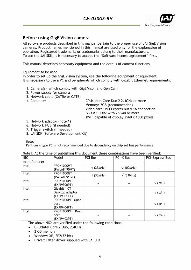
All software products described in this manual pertain to the proper use of JAI GigE Vision cameras. Product names mentioned in this manual are used only for the explanation of operation. Registered trademarks or trademarks belong to their manufacturers. To use the JAI SDK, it is necessary to accept the “Software license agreement” first. This manual describes necessary equipment and the details of camera functions. Equipment to be used In order to set up the GigE Vision system, use the following equipment or equivalent. It is necessary to use a PC and peripherals which comply with Gigabit Ethernet requirements.
1. Camera(s) which comply with GigE Vison and GenICam 2. Power supply for camera 3. Network cable (CAT5e or CAT6) 4. Computer CPU: Intel Core Duo 2 2.4GHz or more Memory: 2GB (recommended) Video card: PCI Express Bus x 16 connection VRAM : DDR2 with 256MB or more DVI : capable of display 2560 x 1600 pixels 5. Network adaptor (note 1) 6. Network HUB (if needed) 7. Trigger switch (If needed) 8. JAI SDK (Software Development Kit) Note: Pentium 4 type PC is not recommended due to dependency on chip set bus performance.
Note1: At the time of publishing this document these combinations have been verified:
NIC manufacturer
Model PCI Bus PCI-X Bus PCI-Express Bus
Intel PRO/1000MT (PWLA8490MT)
(33MHz) (100MHz)
Intel PRO/1000GT (PWLA8391GT)
(33MHz) (33MHz)
Intel PRO/1000PT (EXPI9300PT)
( x1 )
Intel Gigabit CT Desktop adaptor (EXPI9301CT)
( x1 )
Intel PRO/1000PT Quad port (EXPI9404PT)
( x4 )
Intel PRO/1000PT Dual port (EXPI9402PT)
( x4 )
The above NICs are verified under the following conditions.
CPU:Intel Core 2 Duo, 2.4GHz
2 GB memory
Windows XP, SP2(32 bit)
Driver: Filter driver supplied with JAI SDK
CM-030GE-RH
7
Software installation
The JAI SDK & Control Tool for GigE Vision can be downloaded from the JAI web site at www.jai.com. The JAI SDK is available for Windows XP and Vista, 32bit and 64 bit. As for the details of software installation, please refer to the “Getting Started Guide” supplied on the JAI SDK download page.
Camera Operation
1. General The CM-030GE-RH is a 17mm diameter Remote Head camera with 330K pixels on a monochrome progressive scan CCD. This camera achieves a high speed frame rate of 120.491 frames per second. The camera head is small, so it is suitable for such machine vision applications as surface mounting, semiconductor inspection, surface inspection etc.
The 1/3" CCD with square pixels offers a superb image quality. The high-speed shutter function and asynchronous random trigger mode allow the camera to capture high quality images of fast moving objects. The CM-030GE-RH complies with the GenICam standard and contains an internal XML-file that is used to describe the functions/features of the camera. For further information about the GigE Vision standard, please go to www.machinevisiononline.org and about GenICam, please go to www.emva.org. As an application programming interface, JAI provides an SDK (Software Development Kit). This SDK includes the GigE Vision Filter Driver, JAI Control Tool, software documentation and code examples.
2. Camera nomenclature The standard camera composition consists of:
Camera body x 1 Sensor Protection cap x 1
The camera is available in the following versions: CM-030GE-RH Where C stands for "Compact" family, M stands for "Monochrome", 30 represents the resolution "330K pixels", and GE for GigE Vision interface Options: OP735 Lens f=7.5mm, F=1.6 OP715 Lens f=15mm, F=2.0 OP724 Lens f=24mm, F=3.1 PD-12U series AC power adapter

CM-030GE-RH
8
3. Main Features
φ17mm Remote head system with 1/3 inch progressive CCD
GigE Vision and GenICam compliant
High frame rate of 120 fps in Continuous mode, full resolution
659 (h) x 494 (v) active pixels
7.4 µm square pixels
120 frames/second with external trigger and full resolution
Up to 504 frames/second with partial scan of 1/8
193 frames/second with vertical binning
Shutter speed from 32.48μs to 2 sec. using Pulse Width Control
Programmable exposure from 32.48μs to 8.299 ms by 1 LVAL (16.24µs) increments
Pre-select, Pulse Width and RCT trigger modes
LVAL-synchronous/-asynchronous operation (auto-detect)
10 or 8-bit output
Comprehensive software tools and SDK for Windows XP/Vista (32 bit “x86” and 64 bit “x64” JAI SDK Ver. 1.2.1 and after )
CM-030GE-RH
9
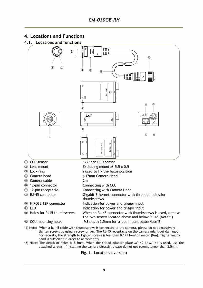
4. Locations and Functions
4.1. Locations and functions
① CCD sensor 1/2 inch CCD sensor
② Lens mount Excluding mount M15.5 x 0.5
③ Lock ring Is used to fix the focus position
④ Camera head φ17mm Camera Head
⑤ Camera cable 2m
⑥ 12-pin connector Connecting with CCU
⑦ 12-pin receptacle Connecting with Camera Head
⑧ RJ-45 connector Gigabit Ethernet connector with threaded holes for thumbscrews
⑨ HIROSE 12P connector Indication for power and trigger input
⑩ LED Indication for power and trigger input
⑪ Holes for RJ45 thumbscrews When an RJ-45 connector with thumbscrews is used, remove the two screws located above and below RJ-45 (Note*1)
⑫ CCU mounting holes M3 depth 3.5mm for tripod mount plate(Note*2)
*1) Note: When a RJ-45 cable with thumbscrews is connected to the camera, please do not excessively tighten screws by using a screw driver. The RJ-45 receptacle on the camera might get damaged. For security, the strength to tighten screws is less than 0.147 Newton meter (Nm). Tightening by hand is sufficient in order to achieve this.
*2) Note: The depth of holes is 3.5mm. When the tripod adapter plate MP-40 or MP-41 is used, use the attached screws. If installing the camera directly, please do not use screws longer than 3.5mm.
Fig. 1. Locations ( version)
G ig E
POWER /TRIG
FCCseal
Serial
No.
Caution
seal
⑦⑧
⑨
⑩
⑪
⑫
⑫
Seria
l No.Z
① ②③ ④ ⑤
⑥
CM-030GE-RH
10
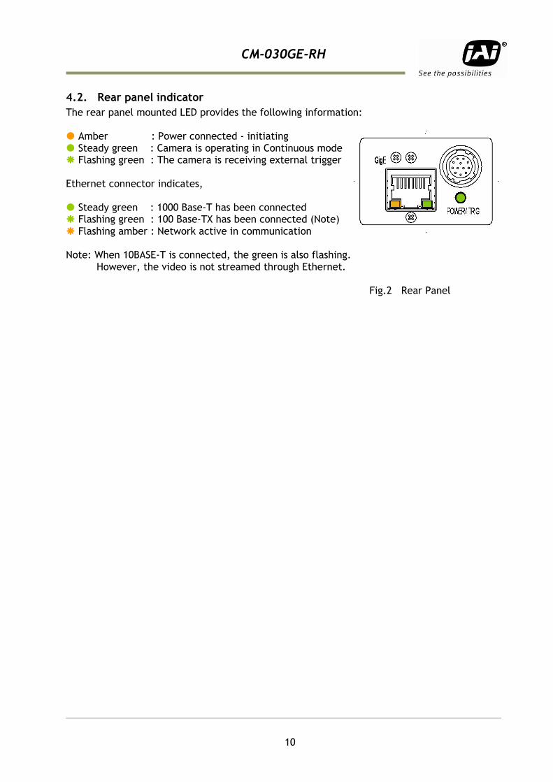
4.2. Rear panel indicator
The rear panel mounted LED provides the following information: Amber : Power connected - initiating Steady green : Camera is operating in Continuous mode Flashing green : The camera is receiving external trigger Ethernet connector indicates, Steady green : 1000 Base-T has been connected Flashing green : 100 Base-TX has been connected (Note) Flashing amber : Network active in communication Note: When 10BASE-T is connected, the green is also flashing.
However, the video is not streamed through Ethernet.
Fig.2 Rear Panel
CM-030GE-RH
11
5. Pin Assignment
5.1. 12-pin Multi-connector (DC-in/GPIO/Iris Video)
Type: HR10A-10R-12PB (Hirose) male. (Seen from rear of camera)
Fig. 3. 12-pin connector.
5.2. Digital Output Connector for Gigabit Ethernet
Type: RJ-45 HFJ11-1G02E-L21RL or equivalent The CM-030GE-RH camera also accepts industrial RJ-45 connectors with thumbscrews. This assures that the connector does not come undone in tough industrial environments. Please contact the nearest JAI distributor for details on recommended industrial RJ-45 connectors.
Fig. 4. Gigabit Ethernet connector The digital output signals follow the Gigabit Ethernet interface using RJ-45 conforming connector. The following is pin assignment for Gigabit Ethernet connector.
Pin No In/Out Name
1 In/Out MX1+ (DA+)
2 In/Out MX1- (DA-)
3 In/Out MX2+ (DB+)
4 In/Out MX3+ (DC+)
5 In/Out MX3- (DC-)
6 In/Out MX2- (DB-)
7 In/Out MX4+ (DD+)
8 In/Out MX4- (DD-)
Pin no. Signal Remarks
1 GND
2 +12 V DC input
3 Opt IN 2 (-)
GPIO IN / OUT
4 Opt IN 2 (+)
5 Opt IN 1 ( - )
6 Opt IN 1 ( + )
7 Opt Out 1 ( - )
8 Opt Out 1 ( + )
9 Opt Out 2 ( - )
10 Opt Out 2 ( + )
11 + 12 V DC input
12 GND
3
456
7
8
9
10
11 12
1
2

CM-030GE-RH
12
6. GPIO (General purpose inputs and outputs)
In chapter 6, there are some examples of settings. the values shown in these examples may need to be adjusted to fit the pixel clock specifications of this particular model.
6.1. Overview
All input and output signals pass through the GPIO (General Purpose Input and Output) module. The GPIO module consists of a Look-Up Table (LUT – Cross-Point Switch), 4 Pulse Generators and a 12-bit counter. In the LUT, the relationship between inputs, counters and outputs is governed by internal register set-up.
On the above block diagram, Trigger 0 is used for Exposure and Trigger 1 is used for Delayed Readout. The Time Stamp Reset can reset the time stamp in compliance with the GigE Vision standard. This is used for having the same time stamp in the case of using multiple cameras. The blocks shown in the above diagram have the following functionality:
6.1.1 LUT (Look Up Table)
The LUT works as a cross-point switch, which allows connecting inputs and outputs freely. The signals LVAL_IN, DVAL_IN, FVAL_IN and EEN_IN all originate from the camera timing circuit. Trigger 0 is connected to the camera's timing circuit and is used for initiating triggered exposure. Trigger 1 is used for Delayed Readout mode. The Time Stamp Reset signal is used reset the camera's time stamp function, also making it possible to reset and synchronize the time stamp of multiple cameras.
LUT
( Cross Point Switch )
Pulse Generator 1(20 bit Counter )
Pulse Generator 0(20 bit Counter )
12 bitCounter
TRIGGER 0
TRIGGER 1
PORT 1 (OPT OUT 1)
PORT 2 (OPT OUT 2)
Time Stamp Reset
LVAL IN
DVAL IN
FVAL IN
EEN IN
PORT IN(OPT IN) 1
PORT IN(OPT IN) 2
Soft Trigger 0
Soft Trigger 1
Soft Trigger 2
Soft Trigger 3
INOUT
Pulse Generator 0
Pulse Generator 1
Pulse Generator 0
Pulse Generator 1
Digital I/O(GPIO) setting
0
1
2
3
4
5
12
13
14
15
16
17
Digital I/O(GPIO) setting
Setting for Line Source
Setting for Line Selector
25 MHz
Pixel Clock
Counter Clock Source
0
1
Counter Divide by value
1/2 to 1/4096
Bypass0
1 - 4095
Pulse Generator Setting 0
Start Point Counter 0 ( 1)Length counter 0
Start Point Counter 0 (2) for repeatEnd point counter 0Counter 0 clear
Pulse Generator Setting 1
Pulse Generator 1
Pulse Generator 1
18
19
Pulse Generator 2
Pulse Generator 3
Pulse Generator Setting 2
Pulse Generator Setting 3
Pulse Generator 2(20 bit Counter )
Pulse Generator 3(20 bit Counter )

CM-030GE-RH
13
6.1.2 12-bit Counter
A 25 MHz clock or the camera pixel clock (58 MHz) can be used as a source. The counter has a “Divide by N”, where N has the range 1 through 4096, allowing a wide range of clock frequencies to be programmed. Setting Value 0 is bypass, setting value 1 is 1/2 dividing and setting value 4095 is 1/4096 dividing.
6.1.3 Pulse Generators (0 to 3)
Each pulse generator consists of a 20-bit counter. The behavior of these signals is defined by their pulse width, start point, end point and number of repetitions. The pulse generator signals can be set in either triggered or periodic mode. In triggered mode, the pulse is triggered by the rising edge/falling edge/high level or low level of the input signal. In periodic mode, the trigger continuously generates a signal that is based on the configured pulse width, starting point and end point.
6.2. Opto-isolated Inputs/Outputs
The control interface of the C3 GigE Vision camera series has opto-isolated inputs and outputs, providing galvanic separation between the camera's inputs/outputs and peripheral equipment. In addition to galvanic separation, the opto-isolated inputs and outputs can cope with a wide range of voltages; the voltage range for inputs is +3.3V to +24V DC whereas outputs will handle +5V to +24V DC. The below figure shows the functional principle (opto-coupler) of the opto-isolated inputs/outputs.
Fig.5. Opto-coupler
6.2.1 Recommended External Input circuit diagram for customer
Fig.6 External Input Circuit, OPT IN 1 and 2
CM-030GE-RH
14
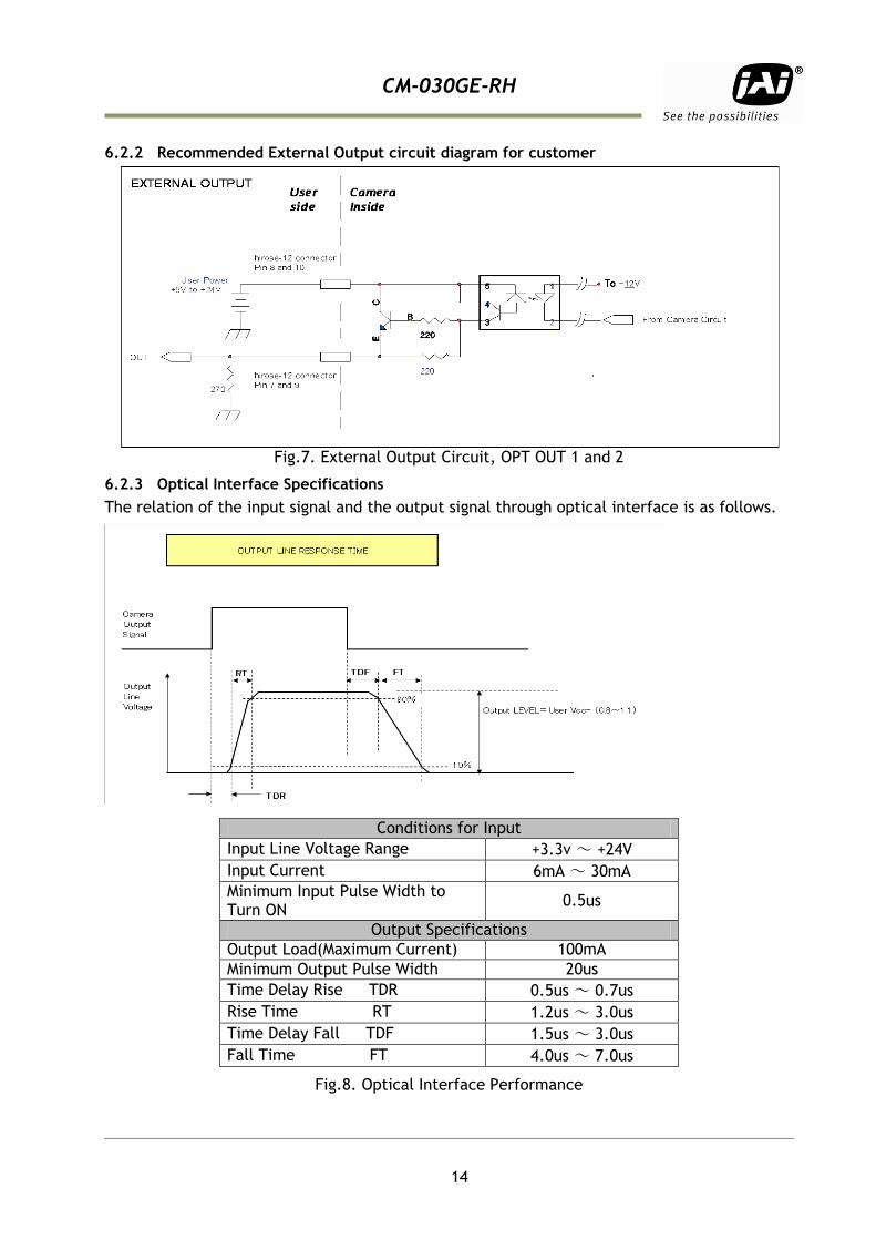
6.2.2 Recommended External Output circuit diagram for customer
Fig.7. External Output Circuit, OPT OUT 1 and 2
6.2.3 Optical Interface Specifications
The relation of the input signal and the output signal through optical interface is as follows.
Conditions for Input
Input Line Voltage Range +3.3v ~ +24V
Input Current 6mA ~ 30mA
Minimum Input Pulse Width to Turn ON
0.5us
Output Specifications
Output Load(Maximum Current) 100mA
Minimum Output Pulse Width 20us
Time Delay Rise TDR 0.5us ~ 0.7us
Rise Time RT 1.2us ~ 3.0us
Time Delay Fall TDF 1.5us ~ 3.0us
Fall Time FT 4.0us ~ 7.0us
Fig.8. Optical Interface Performance
CM-030GE-RH
15
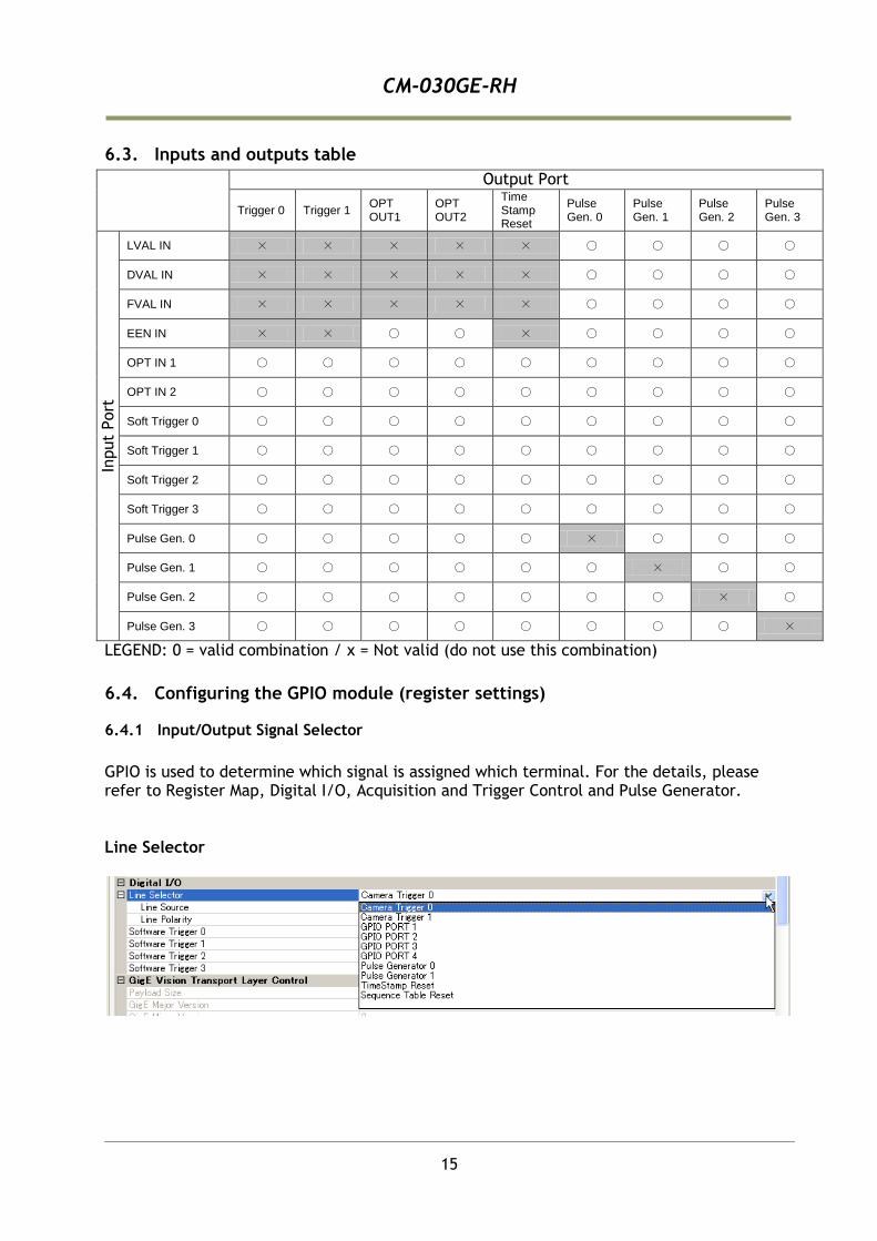
6.3. Inputs and outputs table
Output Port
Trigger 0 Trigger 1 OPT OUT1
OPT OUT2
Time Stamp Reset
Pulse Gen. 0
Pulse Gen. 1
Pulse Gen. 2
Pulse Gen. 3
Input
Port
LVAL IN × × × × × ○ ○ ○ ○
DVAL IN × × × × × ○ ○ ○ ○
FVAL IN × × × × × ○ ○ ○ ○
EEN IN × × ○ ○ × ○ ○ ○ ○
OPT IN 1 ○ ○ ○ ○ ○ ○ ○ ○ ○
OPT IN 2 ○ ○ ○ ○ ○ ○ ○ ○ ○
Soft Trigger 0 ○ ○ ○ ○ ○ ○ ○ ○ ○
Soft Trigger 1 ○ ○ ○ ○ ○ ○ ○ ○ ○
Soft Trigger 2 ○ ○ ○ ○ ○ ○ ○ ○ ○
Soft Trigger 3 ○ ○ ○ ○ ○ ○ ○ ○ ○
Pulse Gen. 0 ○ ○ ○ ○ ○ × ○ ○ ○
Pulse Gen. 1 ○ ○ ○ ○ ○ ○ × ○ ○
Pulse Gen. 2 ○ ○ ○ ○ ○ ○ ○ × ○
Pulse Gen. 3 ○ ○ ○ ○ ○ ○ ○ ○ ×
LEGEND: 0 = valid combination / x = Not valid (do not use this combination)
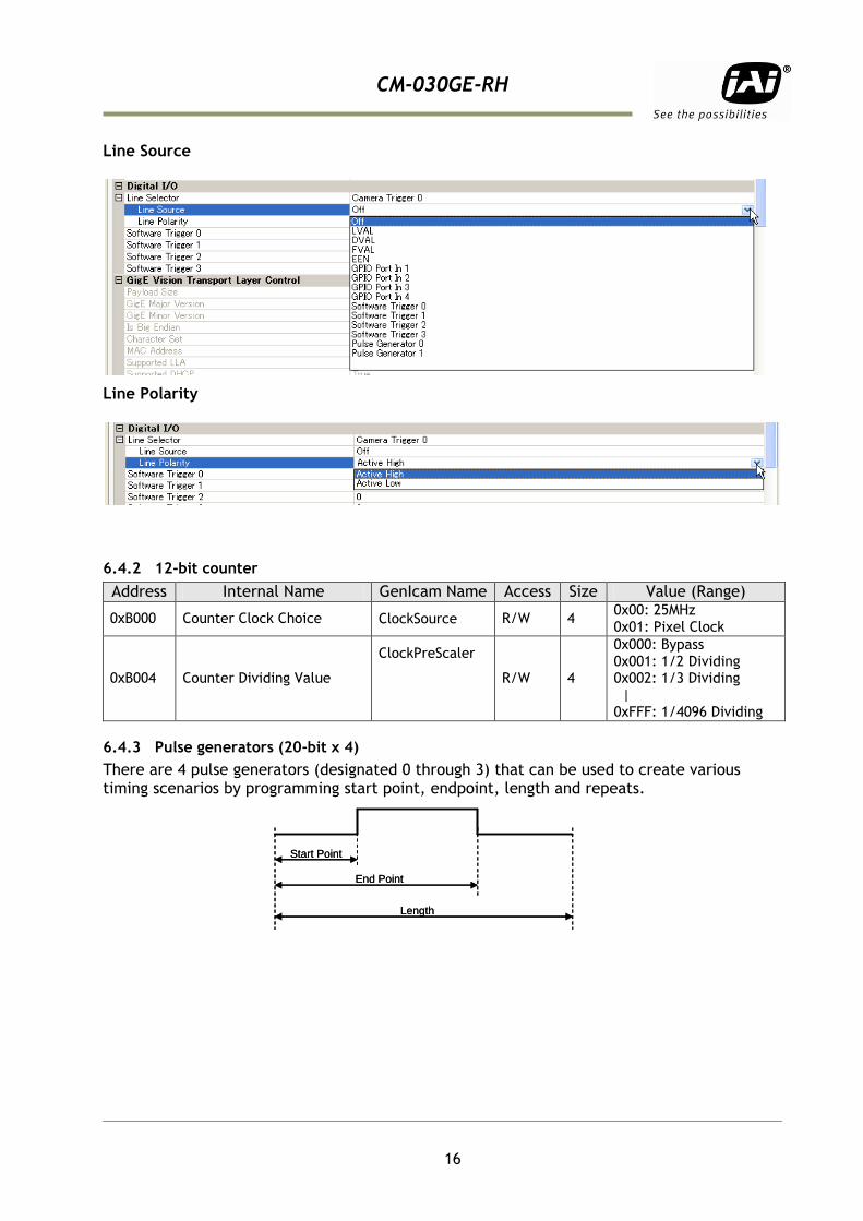
6.4. Configuring the GPIO module (register settings)
6.4.1 Input/Output Signal Selector
GPIO is used to determine which signal is assigned which terminal. For the details, please refer to Register Map, Digital I/O, Acquisition and Trigger Control and Pulse Generator. Line Selector
CM-030GE-RH
16
Start Point
End Point
Length
Start Point
End Point
Length
Line Source
Line Polarity
6.4.2 12-bit counter
Address Internal Name GenIcam Name Access Size Value (Range)
0xB000 Counter Clock Choice ClockSource R/W 4 0x00: 25MHz 0x01: Pixel Clock
0xB004 Counter Dividing Value
ClockPreScaler
R/W 4
0x000: Bypass 0x001: 1/2 Dividing 0x002: 1/3 Dividing | 0xFFF: 1/4096 Dividing
6.4.3 Pulse generators (20-bit x 4)
There are 4 pulse generators (designated 0 through 3) that can be used to create various timing scenarios by programming start point, endpoint, length and repeats.

CM-030GE-RH
17
The following example shows the FVAL input to a pulse generator. The pulse generator creates the pulse using FVAL and the pulse is output through GPIO PORT 1.
Fig 9. Pulse generator setting example
The created pulse rises up at the start point and falls down at the end point, as shown above. Accordingly, the High duration is (End point – Start point) clocks x (1/Pulse gen. frequency). In the above example, the original oscillation uses pixel clock (60 MHz) and the pixel clock is divided by 2400. A pulse frequency of the generator is 25 KHz (60000000/2400). As the start point is 0 and the end point is 99, a pulse having 100 x 1/25000 = 4ms width is created. If the High duration needs to be delayed against an incoming trigger, the start point should be set at “N”. The delay value is N x (1/ 25000). In the above example, the N is “0” which is no delay. The length, in this case, is 102 clocks. These settings can be achieved by using the JAI Control tool which is part of the JAI SDK.
Pulse Generator 0 IN
(FVAL )
0 1 2 3
1
99 100 101 102 103
2 1
Start Point = 0 End Point = 99
Length = 102
Clock IN
Clock Source=Pixel Clock ( 60MHz)
Clock Pre-scaler = 2399 ⇒ 25KHz
1/25KHz = 40µs
Pulse Generator Clear = 4: Rising Edge
Pulse Generator 0 OUT
(GPIO Port 1 )
Repeat counter: 0 to 255
=0: Continuously repeated
Pulse Generator Setting Example

CM-030GE-RH
18
6.5. GPIO programming examples
6.5.1 GPIO Plus PWC shutter
Example: 10µs unit pulse width exposure control (PWC). Pixel clock is 58MHz. 580 clocks (680-100) equals 10µs.
Address Register Value
0xA040 Trigger Mode 2 = PWC ( Pulse Width Control)
① 0xB090 Pulse Generator 0 Selector 4 =OPT IN 1
② 0xB000 Clock Choice 1 = Pixel Clock (58MHz)
0xB004 Counter Dividing Value 0 = Pass through
0xB008 Length Counter 0 1000 Clocks
0xB00C Start point Counter 0 100 Clocks
0xB010 Repeat Count 0 1
0xB014 End point Counter 0 680 Clocks
0xB018 Counter Clear 0 4 = Rising Edge Clear
③ 0xB060 CAMERA TRIGGER Selector 16 = pulse generator 0
Fig.10. Pulse Generator Timing Example 1
LUT
( Cross Point Switch )
Pulse Generator 1(20 bit Counter )
Pulse Generator 0(20 bit Counter )
12 bitCounter
TRIGGER 0
TRIGGER 1
PORT 1 (OPT OUT 1)
PORT 2 (OPT OUT 2)
Time Stamp Reset
LVAL IN
DVAL IN
FVAL IN
EEN IN
PORT IN(OPT IN) 1
PORT IN(OPT IN) 2
Soft Trigger 0
Soft Trigger 1
Soft Trigger 2
Soft Trigger 3
INOUT
Pulse Generator 0
Pulse Generator 1
Pulse Generator 0
Pulse Generator 1
Digital I/O(GPIO) setting
0
1
2
3
4
5
12
13
14
15
16
17
Digital I/O(GPIO) setting
Setting for Line Source
Setting for Line Selector
25 MHz
Pixel Clock
Counter Clock Source
0
1
Counter Divide by value
1/2 to 1/4096
Bypass0
1 - 4095
Pulse Generator Setting 0
Start Point Counter 0Length counter 0
Repeat Counter 0 End point counter 0Counter 0 clear
Pulse Generator 1
Pulse Generator 1
18
19
Pulse Generator 2
Pulse Generator 3
Pulse Generator 2(20 bit Counter )
Pulse Generator 3(20 bit Counter )
1000100
1
680
4
PULSE Generator 0
OUT100
680
1000
CM-030GE-RH
19
Pulse Generator 0
100 Line
500 Line
1000 Line
outputPulse Generator 0
100 Line
500 Line
1000 Line
output
6.5.2 Internal Trigger Generator
Create a trigger signal and trigger the camera
Fig.11. Pulse Generator 0 timing Example 2
LUT
( Cross Point Switch )
Pulse Generator 1(20 bit Counter )
Pulse Generator 0(20 bit Counter )
12 bitCounter
TRIGGER 0
TRIGGER 1
PORT 1 (OPT OUT 1)
PORT 2 (OPT OUT 2)
Time Stamp Reset
LVAL IN
DVAL IN
FVAL IN
EEN IN
PORT IN(OPT IN) 1
PORT IN(OPT IN) 2
Soft Trigger 0
Soft Trigger 1
Soft Trigger 2
Soft Trigger 3
INOUT
Pulse Generator 0
Pulse Generator 1
Pulse Generator 0
Pulse Generator 1
Digital I/O(GPIO) setting
0
1
2
3
4
5
12
13
14
15
16
17
Digital I/O(GPIO) setting
Setting for Line Source
Setting for Line Selector
25 MHz
Pixel Clock
Counter Clock Source
0
1
Counter Divide by value
1/2 to 1/4096
Bypass0
1 - 4095
Pulse Generator Setting 0
Start Point Counter 0Length counter 0
Repeat Counter 0 End point counter 0Counter 0 clear
Pulse Generator 1
Pulse Generator 1
18
19
Pulse Generator 2
Pulse Generator 3
Pulse Generator 2(20 bit Counter )
Pulse Generator 3(20 bit Counter )
1000100
0
500
0
Address Register Value
0xA040 Trigger Mode 1 = EPS
① 0xB000 Clock Choice 1 = Pixel Clock
0xB004 Counter Dividing Value 1829= 1/1830 dev(Line Rate)
0xB008 Length Counter 0 1000 Clocks
0xB00C Start point Counter 0 100 Clocks
0xB010 Repeat Count 0 0 = Free Run
0xB014 End point Counter 0 500 Clocks
0xB018 Counter Clear 0 0 = No Clear
② 0xB060 CAMERA TRIGGER Selector 11 = pulse generator 0
CM-030GE-RH
20
Analog Signal [mV]
Black Level
1023
890
32
025 700
DigitalOut[LSB]
White Clip Level
100% Level
800
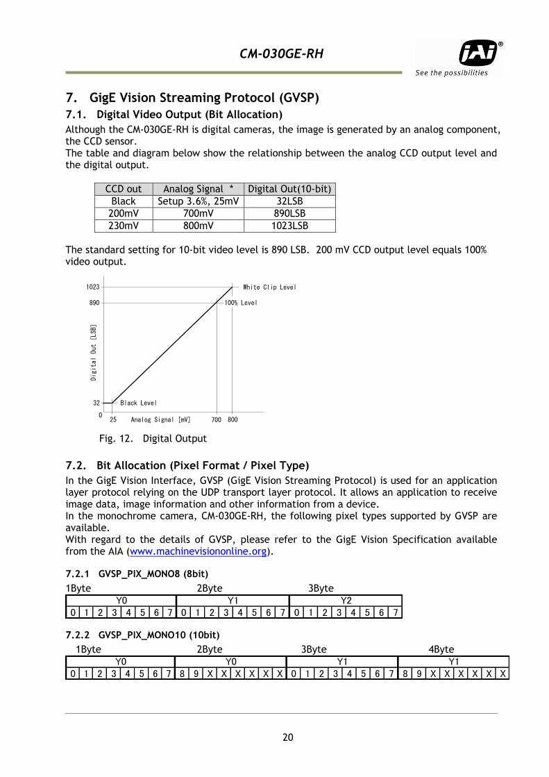
7. GigE Vision Streaming Protocol (GVSP)
7.1. Digital Video Output (Bit Allocation)
Although the CM-030GE-RH is digital cameras, the image is generated by an analog component, the CCD sensor. The table and diagram below show the relationship between the analog CCD output level and the digital output.
CCD out Analog Signal * Digital Out(10-bit)
Black Setup 3.6%, 25mV 32LSB
200mV 700mV 890LSB
230mV 800mV 1023LSB
The standard setting for 10-bit video level is 890 LSB. 200 mV CCD output level equals 100% video output. Fig. 12. Digital Output
7.2. Bit Allocation (Pixel Format / Pixel Type)
In the GigE Vision Interface, GVSP (GigE Vision Streaming Protocol) is used for an application layer protocol relying on the UDP transport layer protocol. It allows an application to receive image data, image information and other information from a device. In the monochrome camera, CM-030GE-RH, the following pixel types supported by GVSP are available. With regard to the details of GVSP, please refer to the GigE Vision Specification available from the AIA (www.machinevisiononline.org).
7.2.1 GVSP_PIX_MONO8 (8bit)
1Byte 2Byte 3Byte
0 1 2 3 4 5 6 7 0 1 2 3 4 5 6 7 0 1 2 3 4 5 6 7Y0 Y1 Y2
7.2.2 GVSP_PIX_MONO10 (10bit)
1Byte 2Byte 3Byte 4Byte
0 1 2 3 4 5 6 7 8 9 X X X X X X 0 1 2 3 4 5 6 7 8 9 X X X X X XY0 Y0 Y1 Y1

CM-030GE-RH
21
7.2.3 GVSP_PIX_MONO10_PACKED (10 bit)
Address Internal Name Access Size Value
0xA410 Pixel Format type R/W 4 0x01080001:Mono8 0x01100003:Mono10 0x010C0004:Mono10 Packed
2 3 4 5 6 7 8 9 0 1 X X 0 1 X X 2 3 4 5 6 7 8 9 2 3 4 5 6 7 8 9 0 1 X X 0 1 X X 2 3 4 5 6 7 8 9
Y3Y1Y0 Y2
CM-030GE-RH
22
8. Functions and Operations
8.1. GigE Vision Standard Interface
The CM-030GE-RH is designed in accordance with the GigE Vision standard. Digital images are transmitted over Cat5e or Cat6 Ethernet cables. All camera functions are also controlled via the GigE Vision interface. The camera can operate in continuous mode, providing an endless stream of images. For capturing individual images related to a specific event, the camera can also be triggered. For precise triggering, it is recommended to use a hardware trigger applied to the Hirose 12-pin connector. It is also possible to initiate a software trigger through the GigE Vision interface. However, when using software trigger, certain latency inherent to the GigE interface must be expected. This latency, which manifests itself as jitter, greatly depends on the general conditions and traffic on the GigE connection. The frame rate described in this manual is for the ideal case and may deteriorate depending on conditions.
When using multiple cameras (going through a switch and/or a single path) or when operating in a system with limited transmission bandwidth the Delayed Readout Mode and Inter-Packet Delay functions can be useful.
8.2. Recommended Network Configurations
Although the CM-030GE-RH conforms to Gigabit Ethernet (IEEE 802.3) not all combinations of network interface cards (NICs) and switches/routers are suitable for use with the GigE Vision compliant camera. JAI will endeavor to continuously verify these combinations, in order to give users the widest choice of GigE components for their system design. Refer to Before using GigE Vision camera.
8.2.1 Guideline for network settings
To ensure the integrity of packets transmitted from the camera it is recommended to follow these simple guidelines:
1. Whenever possible use a peer-to-peer network. 2. When connecting several cameras, going through a network switch, make sure it is
capable of handling jumbo packets and that it has sufficient memory capacity. 3. Configure inter-packet delay to avoid congestion in networks switches. 4. Disable screen saver and power save functions on computers. 5. Use high performance computers with multi-CPU, hyper-thread and 64-bit CPU, etc. 6. Only use Gigabit Ethernet equipment and components together with the camera. 7. Use at least Cat5e or preferably Cat6 Ethernet cables. 8. Whenever possible, limit the camera output to 8-bit.
8.2.2 Video data rate (network bandwidth)
The video bit rate for the CM-030GE-RH is:
In case of using Jumbo Frames, the packet data will be improved by 2 %. For CM-030GE-RH, Jumbo Frames can be set at a maximum of 4040 Bytes (Factory setting is 1428 Bytes).
Model Pixel Type Packet data volume (In case the Packet size is 1500)
CM-030GE-RH
MONO8 324 Mbit/s
MONO10_PACKED 486 Mbit/s
MONO10 648 Mbit/s

CM-030GE-RH
23
8.2.3 Note for 100BASE-TX connection
In case of connecting on 100BASE-TX, the maximum packet size should be 1500 bytes.
In case of connecting on 100BASE-TX, the specifications such as frame rate, trigger interval etc. described in this manual cannot be satisfied.
Depending on network conditions or the PC used, the following frame rate may not be achieved.
100BASE-T works in FULL DUPLEX. It does not work in HALF DUPLEX.
8.3. Basic functions
The CM-030GE-RH camera is a 17mm diameter small remote head camera with 330K pixels on a monochrome progressive CCD. The length between the camera head and the CCU is 2m and the cable is attached to the camera head. The frame rate is as high as 120.491 fps. The external trigger pulse is input via HIROSE 12-pin connector. In trigger modes, a frame rate of 120 fps can be achieved. There are 5 trigger modes in addition to continuous operation. They are: Edge Pre-Select, Pulse Width Control, RCT, Sequence Trigger and Frame Delay Trigger.
8.3.1 Partial scan
Partial scan mode is a scanning system used to read out the center portion of the image in order to make the frame rate faster. As shown in the drawing below, the first and last part of the full frame is read out using a fast dump method enabling a faster frame rate for capturing images that don’t require the full frame height. CM-030GE-RH has preset partial scans of 2/3, 1/2, 1/4 and 1/8 frame height.
Fig. 13 Partial scan
Fast Dump
Fast Dump
Normal Scan
Mode Start line End line Frame rate
2/3
1/2
1/4
1/8
83
123
185
215
410
368
306
274
172.97 fps
216.80 fps
349.83 fps
504.72 fps
Pixel Type Frame rate at Full Frame[fps]
MONO8, BAYRG8, BAYGB8 36.6 ~ 36.8
MONO10_PACKED 24.4
MONO10, BAYRG10, BAYGB10 18.2 ~ 18.4

CM-030GE-RH
24
8.3.2 Vertical Binning
Binning mode is a function where the signal charge from 2 adjacent (vertical) pixels are added together and read out as one pixel. Binning results in half vertical resolution and a higher frame rate. In addition, by adding 2 pixels together, the sensitivity is doubled. The charge accumulated in 2 adjacent lines is added together in the horizontal CCD register. This is done by providing two pulses to the vertical CCD register for each line read out. Vertical binning cannot be used together with partial scanning.
Fig. 14 Vertical Binning
8.3.3 Electronic Shutter
The CM-0303PMCL-RH has three methods for selecting the shutter speed: preset shutter (10 fixed steps), programmable exposure (from 2 to 511 lines in one-line increments) and GenICam standard Exposure Time Abs.
Preset Shutter The following shutter speeds can be selected by command SH=0 through SH=9. OFF (1/120), 1/250, 1/500, 1/1000, 1/2000, 1/4000, 1/8000, 1/10000, 1/15000, 1/30000 seconds
Note1) When the trigger mode is selected in partial scan mode, the shutter off is the same as the exposure time of continuous normal scan mode (511L). If the shorter minimum trigger interval is required, set the exposure time shorter than line number of continuous scan in partial scan mode.
Note2) Preset shutter value is converted to a programmable exposure value inside the camera. Therefore, there is some variance, especially in vertical binning mode.
Preset Shutter
Exposure lines [Line]
Actual exposure
Value[s] FULL (µs) VBinning(µs)
Off(1/120) 511 8299 5158
1/250 246 3995 4937
1/500 123 1998 2468
1/1000 62 1007 1244
1/2000 31 503 622
1/4000 15 244 301
1/8000 8 130 161
1/10000 6 97.4 120
1/15000 4 65 80.3
1/30000 2 32.5 40.1
Normal full scanning
2 line Vertical Binning
H
H
Horizontal CCD Register S/H Reset
Vide
o Out
Xsg1
Vertic
al C
CD
Registe
r
Pixel
CM-030GE-RH
25
Programmable Exposure (PE) The exposure time can be programmed in 16.24µs (LVAL period) increments. The range is from 2 LVAL to 511 LVAL.
Minimum exposure time 2L Maximum exposure time 511L
16.24 µs x 2(L) = 32.48 µs 16.24 µs x 511 (L) ≈ 8.299 ms
In binning mode:
Minimum Exposure time 2L Maximum exposure time 257L
20.069 µs x 2(L) = 40.138 µs 20.069 µs x 257 (L) ≈ 5.158 ms Exposure Time Abs This is a function specified in the GenICam standard. The shutter speed can be entered as an absolute exposure time in microseconds (μs) in register address 0xA018. The entered absolute time (Time Abs) is then converted to a programmable exposure (PE) value inside the camera. The equations below show the relationship between the PE value used by the camera for the different readout modes and the "Exposure Time Abs" value entered in register 0xA018. Due to rounding (decimals rounded down), some discrepancies may occur. The relation between PE value and Time Abs: Normal readout PE= 2 + INT(1) (Exposure time -32.5) µs / (942(2)/58000000(3)) V Binning readout PE= 2 + INT (Exposure time -40.1) µs / (1164/58000000)
Note: (1) INT means integer (rounded down). (2) Pixel clocks/line. (3) Pixel clock
GPIO in combination with Pulse Width Trigger More precise exposure time can be obtained by using the GPIO module in combination with Pulse Width Trigger mode. The clock generator and counter can be programmed in very fine increments. For an example, refer to 6.5.1 GPIO Plus PWC shutter Upper limit and lower limit of exposure time in each read out mode.
Lower limit
Upper limit
µs Line
Normal 32.5µs 8299µs 511L
2/3 Partial 32.5µs 5814µs 358L
1/2 Partial 32.5µs 4677µs 288L
1/4 Partial 32.5µs 2907µs 179L
1/8Partial 32.5µs 2046µs 126L
V Binning 40.1µs 5158µs 257L

CM-030GE-RH
26
8.3.4 Auto-detect LVAL-sync / async accumulation
This function replaces the manual setting found in older JAI cameras. Whether accumulation is synchronous or asynchronous in relation to LVAL depends on the timing of the trigger input. When a trigger is received while FVAL is high (during readout), the camera works in LVAL- synchronous mode, preventing reset feed-through in the video signal. There is a maximum jitter of one LVAL period from issuing a trigger and accumulation start. When a trigger is received during FVAL low, the camera works in LVAL-asynchronous mode (no delay) mode.
This applies to both Edge Pre-select (EPS) trigger mode and Pulse Width Control (PWC) trigger mode.
Ext. trigger
FVAL
(1) (3)
(1) In this period camera executes trigger at next LVAL (prevents feed-through noise) (2) Avoid trigger at FVAL transition (+/- 1 LVAL period), as the function may randomly switch between "next LVAL" and "immediate". (3) In this period camera executes trigger immediately (no delay)
(2)
Fig. 15 Auto-detect LVAL sync /async accumulation
CM-030GE-RH
27
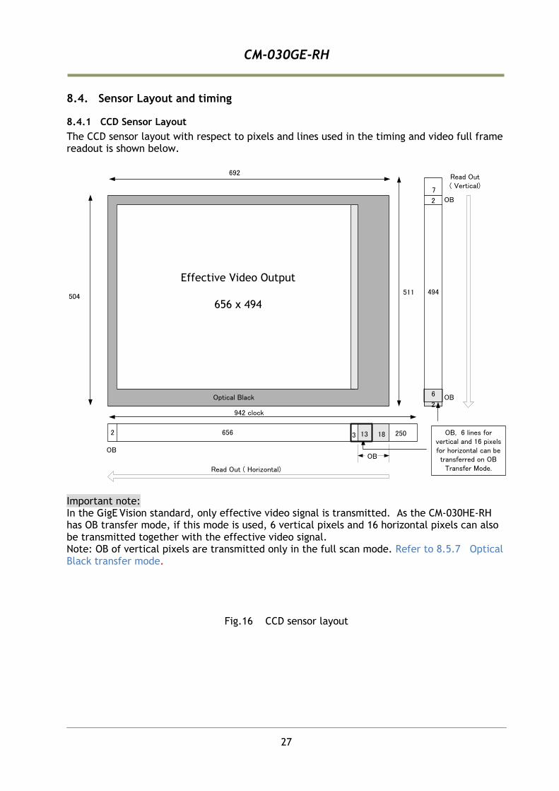
8.4. Sensor Layout and timing
8.4.1 CCD Sensor Layout
The CCD sensor layout with respect to pixels and lines used in the timing and video full frame readout is shown below.
Important note: In the GigE Vision standard, only effective video signal is transmitted. As the CM-030HE-RH has OB transfer mode, if this mode is used, 6 vertical pixels and 16 horizontal pixels can also be transmitted together with the effective video signal. Note: OB of vertical pixels are transmitted only in the full scan mode. Refer to 8.5.7 Optical Black transfer mode.
Fig.16 CCD sensor layout
8
Read Out ( Horizontal)
Read Out ( Vertical)
2 656
494
2
504
OBOB
692
Effective Video Output
656 x 494
OB
OB
6Optical Black
7
511
250
942 clock
3
2
1813 OB, 6 lines for vertical and 16 pixels for horizontal can be transferred on OB
Transfer Mode.
CM-030GE-RH
28
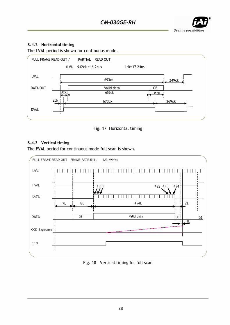
8.4.2 Horizontal timing
The LVAL period is shown for continuous mode.
Fig. 17 Horizontal timing
8.4.3 Vertical timing
The FVAL period for continuous mode full scan is shown.
Fig. 18 Vertical timing for full scan
FULL FRAME READ OUT / PARTIAL READ OUT
1LVAL 942ck =16.24us 1ck=17.24ns
LVAL693ck 249ck
DATA OUT Valid data OB3ck
2ck 673ck 269ck
DVAL
659ck 31ck
CM-030GE-RH
29
8.4.4 Partial Scan
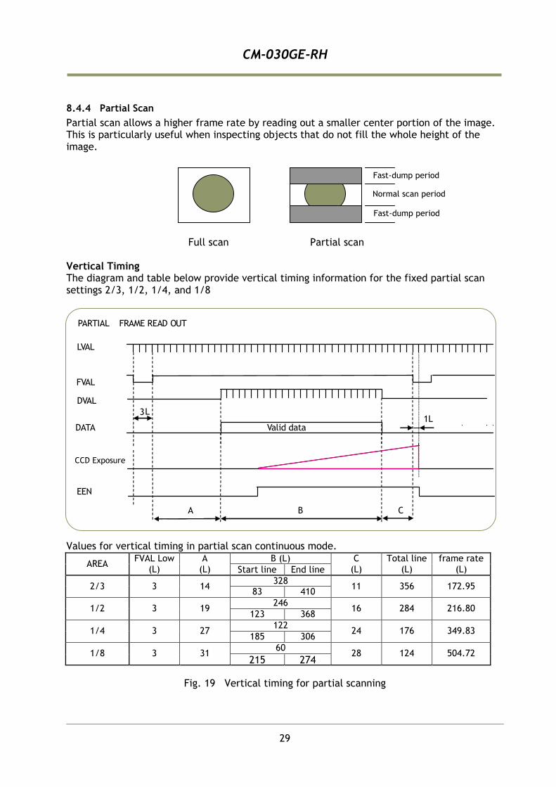
Partial scan allows a higher frame rate by reading out a smaller center portion of the image. This is particularly useful when inspecting objects that do not fill the whole height of the image. Full scan Partial scan Vertical Timing The diagram and table below provide vertical timing information for the fixed partial scan settings 2/3, 1/2, 1/4, and 1/8
Values for vertical timing in partial scan continuous mode.
AREA FVAL Low
(L) A
(L) B (L) C
(L) Total line
(L) frame rate
(L) Start line End line
2/3 3 14 328
11 356 172.95 83 410
1/2 3 19 246
16 284 216.80 123 368
1/4 3 27 122
24 176 349.83 185 306
1/8 3 31 60
28 124 504.72 215 274
Fig. 19 Vertical timing for partial scanning
Fast-dump period
Fast-dump period
Normal scan period
PARTIAL FRAME READ OUT
LVAL
FVAL
DVAL
3L
DATA Valid data
EEN
A B C
1L
CCD Exposure

CM-030GE-RH
30
Horizontal Timing The horizontal timing for partial scanning is the same as for full scanning.
Fig. 20 Horizontal timing for partial scanning
8.4.5 Vertical Binning
Vertical binning combines charge from two adjacent lines, reducing the vertical resolution to half and at the same time increasing frame rate and sensitivity. By activating this function, the frame rate is increased to 193.9 fps. Important Note Vertical Binning cannot be used together with the Partial Scan mode. Horizontal Timing
Fig.21 Horizontal Timing for Vertical Binning
FULL FRAME READ OUT / PARTIAL READ OUT
1LVAL 942ck =16.24us 1ck=17.24ns
LVAL693ck 249ck
DATA OUT Valid data OB3ck
2ck 673ck 269ck
DVAL
659ck 31ck

CM-030GE-RH
31
Vertical timing
Fig.22 Vertical Timing for Vertical Binning
8.5. Operation Modes
This camera can operate in 4 primary modes.
1. Continuous Mode Pre-selected exposure. 2. Edge Pre-select Mode Pre-selected exposure. 3. Pulse Width Control Mode Pulse width controlled exposure. 4. RCT Mode Pre-selected exposure. 5. Sequential trigger mode (EPS) Pre-selected exposure. 6. Frame delay readout (EPS, PWC) 7. OB transfer mode
8.5.1 Continuous operation
For applications not requiring asynchronous external triggering, this mode should be used. For timing details, refer to fig. 17 through fig. 22. To use this mode: Set function: Trigger mode Continuous Scanning Full, partial V Binning ON / OFF Shutter mode Pre-set, programmable, Exposure Time
Abs
CM-030GE-RH
32
8.5.2 Edge Pre-select Trigger Mode
An external trigger pulse initiates the capture, and the exposure time (accumulation time) is defined by preset, programmable or Exposure Time Abs register. The resulting video signal will start to be read out after the selected shutter time. For timing details, refer to fig. 17 through fig. 24. To use this mode: Set function: Trigger mode Edge pre-select Scanning Full, Partial V Binning ON / OFF Shutter mode Edge pre-select, programmable, Exposure Time Abs Input: Ext. trigger. 12-pin Hirose GPIO Important notes on using this mode
1. The minimum trigger interval >2 LVAL. 2. Depending on the timing of the leading edge of the trigger pulse in relationship to
FVAL, accumulation will be synchronous or asynchronous in relationship to LVAL. See 8.3.4 Auto-detect LVAL-sync / async accumulation.
3. The minimum trigger interval is as follows.
Scan mode Minimum interval[L]
Normal Full 513
2/3 Partial 359
1/2 Partial 287
1/4 Partial 179
1/8 Partial 125
Vertical binning 259
Note: In order to keep the minimum trigger interval in the partial scan mode, the
exposure time should not exceed the line number at normal scan. If the exposure time is set longer than that, the trigger interval is longer by (Exposure time – normal scan line number). The maximum exposure time is 511L.
CM-030GE-RH
33
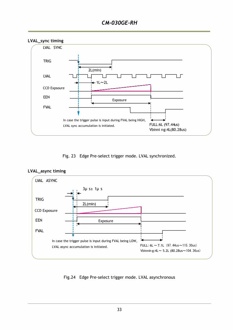
LVAL_sync timing
Fig. 23 Edge Pre-select trigger mode. LVAL synchronized.
LVAL_async timing
Fig.24 Edge Pre-select trigger mode. LVAL asynchronous
LVAL SYNC
TRIG
2L(min)
LVAL
1L~2L
EEN
FVAL
FULL:6L (97.44us)
Vbinni ng:4L(80.28us)
Exposure
CCD Expsoure
In case the trigger pulse is input during FVAL being HIGH,
LVAL sync accumulation is initiated.
LVAL ASYNC
3μ s± 1μ s
TRIG2L(min)
EEN
FVAL
FULL: 6L~ 7.1L(97.44us~115.30us)
Vbinnin g:4L~ 5.2L (80.28us~104.36us)
In case the trigger pulse is input during FVAL being LOW,
LVAL async accumulation is initiated.
Exposure
CCD Exposure
CM-030GE-RH
34
8.5.3 Pulse Width Control Trigger Mode
In this mode the accumulation time is equal the trigger pulse width. Here it is possible to have a long time exposure. The maximum recommended time is <240 frames ( 2 seconds). For timing details, refer to fig. 17 through fig. 22 and fig. 25 & 26. To use this mode: Set function: Trigger mode Pulse width control Scanning Full, Partial Vertical binning ON / OFF Input: Ext. trigger. HIROSE 12-pin GPIO Important notes on using this mode
1. The minimum trigger interval > 2 LVAL 2. Depending on the timing of the leading edge of the trigger pulse in relationship to
FVAL, accumulation will be synchronous or asynchronous in relationship to LVAL. See 8.3.4 Auto-detect LVAL-sync / async accumulation
3. The minimum trigger interval is as follows.
Scan mode Minimum interval[L]
Normal Full 513
2/3 Partial 359
1/2 Partial 287
1/4 Partial 179
1/8 Partial 125
Vertical binning 259
Note: In order to keep the minimum trigger interval in the partial scan mode, the
exposure time should not exceed the line number at normal scan. If the exposure time is set longer than that, the trigger interval is longer by (Exposure time – normal scan line number). The maximum exposure time is 511L.
CM-030GE-RH
35
LVAL_sync timing
Fig. 25 Pulse width trigger mode. LVAL synchronized.
LVAL_async timing
Fig.26 Pulse Width trigger mode. LVAL asynchronous
LVAL ASYNC
3μ s± 1μ s
2L(min)TRIG 1L
EEN
FVAL
FULL: 6L~ 7.1L(97.44us ~ 115.3us)
Vbinnig:4L~5.2L(80.28us ~ 104.36us)
In case the trigger pulse is input during FVAL being LOW,
LVAL async accumulation is initiated.
Exposure
CCD Exposure
LVAL SYNC TRIG
TRIG
LVAL
1L(max)1L
EEN
FVAL
FULL: 6L~ 7.1L(97.44us ~ 115.3us)
Vbinnig:4L~5.2L(80.28us ~ 104.36us)
In case the trigger pulse is input during FVAL being HIGH,
LVAL sync accumulation is initiated.
Exposure
CCD Exposure
Raising prohibited
2L(min)
CM-030GE-RH
36
8.5.4 RCT Trigger mode
The RCT mode operates like EPS (Edge Pre-select) mode with smearless function. An external trigger pulse will immediately stop the video read out, reset and restart the exposure, then operate as normal mode until the next trigger. After the trigger pulse is input, a fast dump read out is performed. In the CM-030GE-RH, this period is 1.0231ms which is 63L. The exposure time is determined by the pre-set shutter speed. If no further trigger pulses are applied, the camera will continue in normal mode and the video signal is not output. The fast dump readout has the same effect as “smearless readout”. Smear above bright areas is reduced for the trigger frame. RCT mode is available only in LVAL asynchronous. Important notes on using this mode
1. When the shutter setting is either PE=511 or OFF, EEN is kept as HIGH. 2. The minimum trigger interval is as follows ( if PE is 2L):
Scan mode Minimum interval[L]
Normal Full 578
2/3 Partial 423
1/2 Partial 351
1/4 Partial 243
1/8 Partial 189
Vertical binning 324
Note: In order to keep the minimum trigger interval in the partial scan mode, the
exposure time should not exceed the line number at normal scan. If the exposure time is set longer than that, the trigger interval is longer by (Exposure time – normal scan line number). The maximum exposure time is 511L.
Fig. 27 RCT mode
TRIG
1.0231 ms (63L)
EEN
FVAL
DVAL
FULL: 6L~7.1L(97.44us ~ 115.30us)
Vbinni ng:4L~5.2L(80.27us ~104.35us)
CCD Exposure
CM-030GE-RH
37
Trigger
Sequence operation
Sequence 1 Sequence 2 Sequence 3 Sequence 4
8.5.5 Sequential Trigger Mode (EPS trigger)
This mode allows the user to define a preset sequence of up to 10 images, each with its own ROI, Shutter and Gain values. As each trigger input is received, the image data with the preset sequence is output as described below.
Signals added to trigger can be selected by 0xB060 Camera Trigger Selector in the register map via GPIO. The camera will functions on the rising edge of the trigger and Negative or Positive should be determined accordingly.
The following default settings can be modified by the user to define a sequence.
ID ROI
Shutter Gain Width Height
Offset X
Offset Y
1 656 494 0 0 511 0
2 656 494 0 0 511 0
3 656 494 0 0 511 0
4 656 494 0 0 511 0
5 656 494 0 0 511 0
6 656 494 0 0 511 0
7 656 494 0 0 511 0
8 656 494 0 0 511 0
9 656 494 0 0 511 0
10 656 494 0 0 511 0
The following registers are used to configure the sequence. 0xC0F4 Sequence Repetitions (Number of Repetitions – Note: 0 = repeat indefinitely) 0xC0F8 Sequence Ending Position (Ending Position) 0xA30C Sequence Reset Command (1 only) 0xB060 Selection for camera trigger 0 0xA040 Trigger mode selection and 0x09 for Sequential EPS mode
Example of settings Setting: Repeat 5 times from ID 1 through ID 8 0xC0F4 Set to 0x05 0xC0F8 Set to 0x08 0xB060 For instance, Pin 6 of the 12-pin Hirose connector for Opto IN 1 0xA040 Sequential PS (9) 0xA3F0 Set this to (1) for start 0xA040 Set Normal Mode to (0) for stop
Note:1) As for the details of register, refer to Register Map. Note:2) It is recommended to set the exposure time in the order from the shortest to the longest one. Note:3) The minimum trigger interval is > Exposure time (expressed in L(Line)) + FVAL on Normal scan ( 511L) +
1L ) Note:4) Do not input the trigger just after the sequence is reset. It requires at least 500ms delay. Note:5) In sequential mode, the exposure should be adjusted so that the LVAL async mode can always
function.
CM-030GE-RH
38
8.5.6 Delayed Readout Mode (EPS and PWC)
This mode can be used to delay the transmission of a captured image. When several cameras are triggered simultaneously and connected to the same GigE interface, it allows the cameras to be read out in sequence, preventing congestion. The image data is not transmitted directly by the trigger 0 and it is stored in the memory located at Ethernet Interface. By the falling edge of the soft trigger 1, the image data is output.
Example of setting 0xA040 PS Delayed Readout (0x11) 0xB060 Trigger 0 select, e.g. 0x04 OPT IN 1 0xB-064 Trigger 1 select, e.g. 0x05 OPT IN 2 For the details of Registers, please refer Camera Register Map which is included in the SDK.
Exposure
CCD output
Store in the GigE memory
Output from GigE
Trigger 0
CCD Photodiode
CCD Transfer gate
GigE memery
Ethernet output
Trigger 1
CM-030GE-RH
39
8.5.7 Optical Black transfer mode
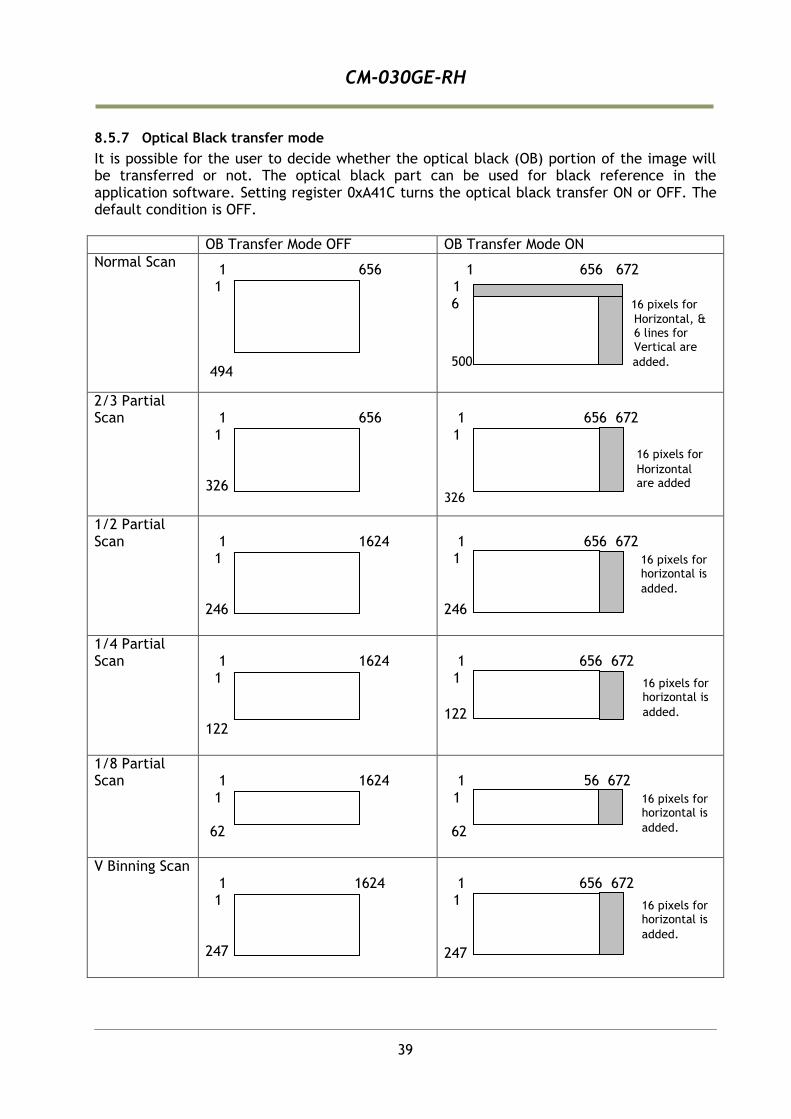
It is possible for the user to decide whether the optical black (OB) portion of the image will be transferred or not. The optical black part can be used for black reference in the application software. Setting register 0xA41C turns the optical black transfer ON or OFF. The default condition is OFF.
OB Transfer Mode OFF OB Transfer Mode ON
Normal Scan
1 656 1 494
1 656 672 1 6 16 pixels for
Horizontal, & 6 lines for Vertical are 500 added.
2/3 Partial Scan
1 656 1 326
1 656 672 1
ます 16 pixels for
Horizontal are added
326
1/2 Partial Scan
1 1624 1 246
1 656 672 1 246
1/4 Partial Scan
1 1624 1 122
1 656 672 1
ます
122
1/8 Partial Scan
1 1624 1 62
1 56 672 1 62
V Binning Scan 1 1624 1 247
1 656 672 1
ます
247
16 pixels for horizontal is
added.
16 pixels for horizontal is
added.
16 pixels for horizontal is
added.
16 pixels for horizontal is
added.
CM-030GE-RH
40
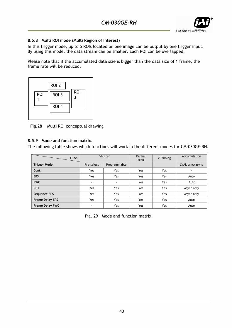
8.5.8 Multi ROI mode (Multi Region of Interest)
In this trigger mode, up to 5 ROIs located on one image can be output by one trigger input. By using this mode, the data stream can be smaller. Each ROI can be overlapped. Please note that if the accumulated data size is bigger than the data size of 1 frame, the frame rate will be reduced.
Fig.28 Multi ROI conceptual drawing
8.5.9 Mode and function matrix.
The following table shows which functions will work in the different modes for CM-030GE-RH.
Func. Shutter
Partial scan
V Binning Accumulation
Trigger Mode Pre-select Programmable LVAL sync/async
Cont. Yes Yes Yes Yes -
EPS Yes Yes Yes Yes Auto
PWC - - Yes Yes Auto
RCT Yes Yes Yes Yes Async only
Sequence EPS Yes Yes Yes Yes Async only
Frame Delay EPS Yes Yes Yes Yes Auto
Frame Delay PWC - Yes Yes Yes Auto
Fig. 29 Mode and function matrix.
ROI
1
ROI 2
ROI
3
ROI 4
ROI 5
CM-030GE-RH
41
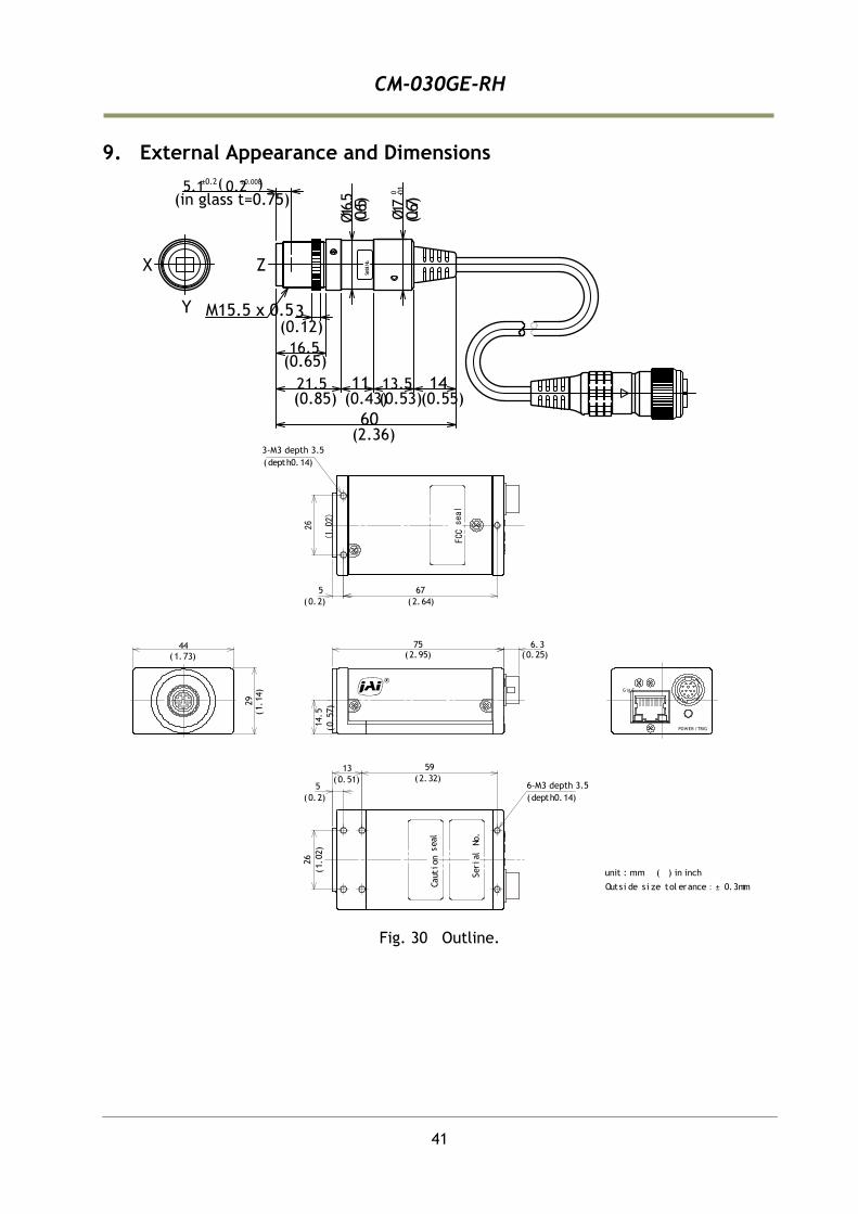
9. External Appearance and Dimensions
Fig. 30 Outline.
(depth0.14)
Outsi de si ze tol erance:± 0.3mm
G ig E
POWER /TRIG
( 2.64)
( 2.95)
( 2.32)
( 0.25)
59
6.375
67
FCCseal
Serial
No.
Caution
seal
( depth0.14)
(0.57)
( 0. 2)
( 0.2)
5( 0.51)
13
(1.02)
(1.02)
26
5
26
14.5(1.14)
( 1. 73)
29
44
6-M3 depth 3.5
3-M3 depth 3.5
unit : mm ( ) in inch
.oNlaireS)56 .0(5.61Ø
M15.5 x 0.53(0.12)
16.5(0.65)
(0.55)(0.53)(0.43)(0.85)21.5 11 13.5 14
(2.36)60
)76.0(71Ø
01.0-
(in glass t=0.75)5.1
±0.20.2
±0.008
X Z
Y
( )
CM-030GE-RH
42
10. Specifications
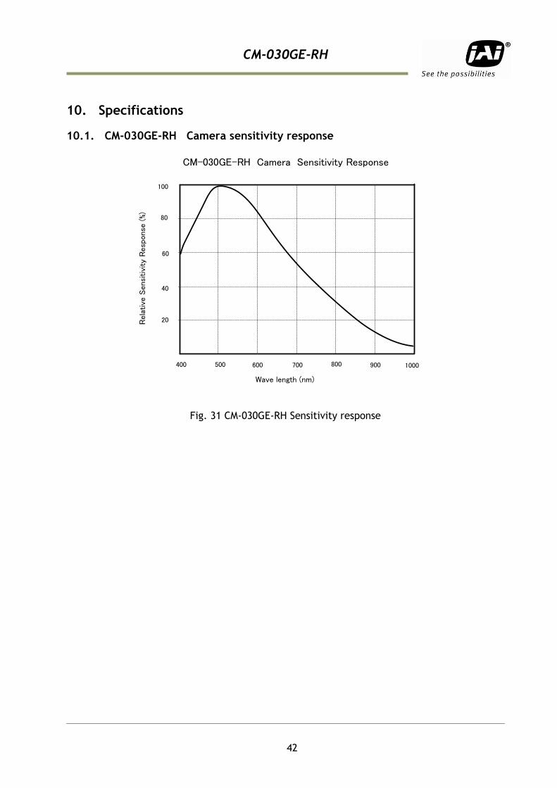
10.1. CM-030GE-RH Camera sensitivity response
Fig. 31 CM-030GE-RH Sensitivity response
100
400 500 600 700 800 900 1000
Rel
ativ
e Sen
sitivi
ty R
espo
nse
(%)
Wave length (nm)
CM-030GE-RH Camera Sensitivity Response
80
60
40
20
CM-030GE-RH
43
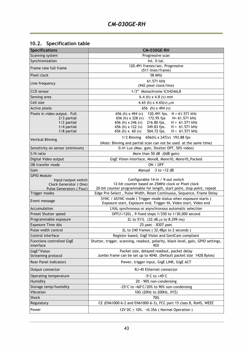
10.2. Specification table
Specifications CM-030GE-RH
Scanning system Progressive scan
Synchronization Int. X-tal.
Frame rate full frame 120.491 frames/sec. Progressive
(511 lines/frame)
Pixel clock 58 MHz
Line frequency 61.571 kHz
(942 pixel clock/line)
CCD sensor 1/3” Monochrome ICX424ALB
Sensing area 6.4 (h) x 4.8 (v) mm
Cell size 4.65 (h) x 4.65(v) m
Active pixels 656 (h) x 494 (v)
Pixels in video output. Full 2/3 partial 1/2 partial 1/4 partial 1/8 partial
656 (h) x 494 (v) 120.491 fps. H = 61.571 kHz 656 (h) x 328 (v) 172.95 fps H= 61.571 kHz
656 (h) x 246 (v) 216.80 fps. H = 61.571 kHz 656 (h) x 122 (v) 349.83 fps. H = 61.571 kHz 656 (h) x 60 (v) 504.72 fps. H = 61.571 kHz
Vertical Binning 1/2 Binning 656(h) x 247(v) 193.88 fps
(Note: Binning and partial scan can not be used at the same time)
Sensitivity on sensor (minimum) 0.41 Lux (Max. gain, Shutter OFF, 50% video)
S/N ratio More than 50 dB (0dB gain)
Digital Video output GigE Vision Interface, Mono8, Mono10, Mono10_Packed
OB transfer mode ON / OFF
Gain Manual -3 to +12 dB
GPIO Module Input/output switch
Clock Generator ( One) Pulse Generators ( Four)
Configurable 14-in / 9-out switch
12-bit counter based on 25MHz clock or Pixel clock 20-bit counter programmable for length, start point, stop point, repeat
Trigger modes Edge Pre-Select , Pulse Width, Reset Continuous, Sequence, Frame Delay
Event message SYNC / ASYNC mode ( Trigger mode status when exposure starts ) Exposure start, Exposure end, Trigger IN, Video start, Video end
Accumulation LVAL synchronous or asynchronous automatic selection
Preset Shutter speed OFF(1/120) , 9 fixed steps 1/250 to 1/30,000 second
Programmable exposure 2L to 511L (32.48 s to 8.299 ms)
Exposure Time Abs 25 µsec – 8307 µsec
Pulse width control 2L to 240 frames ( 32.48µs to 2 seconds )
Control interface Register based, GigE Vision and GenICam compliant
Functions controlled GigE interface
Shutter, trigger, scanning, readout, polarity, black level, gain, GPIO settings, ROI
GigEⓇVision Streaming protocol
Packet size, delayed readout, packet delay Jumbo frame can be set up to 4040. (Default packet size 1428 Bytes)
Rear Panel indicators Power, trigger input, GigE LINK, GigE ACT
Output connector RJ-45 Ethernet connector
Operating temperature -5C to +45C
Humidity 20 – 90% non-condensing
Storage temp/humidity -25C to +60C/20% to 90% non-condensing
Vibration 10G (20Hz to 200Hz, XYZ)
Shock 70G
Regulatory CE (EN61000-6-2 and EN61000-6-3), FCC part 15 class B, RoHS, WEEE
Power 12V DC 10%. <0.35A ( Normal Operation )

CM-030GE-RH
44
Specifications CM-030GE-RH
Lens mount φ17mm Exclusive mount
Dimensions Head φ17 x 46mm ( φ x D ) with 2m cable CCU 44 x 29 x 75 mm (H x W x D)
Weight Head with 2m cable 120g, CCU 130g
Note: Above specifications are subject to change without notice Note: Approximately 30 minutes of warm up required in order to meet specifications.
CM-030GE-RH
45
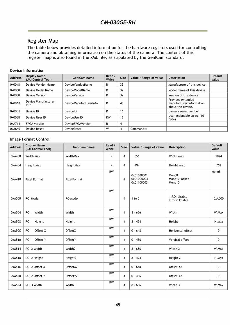
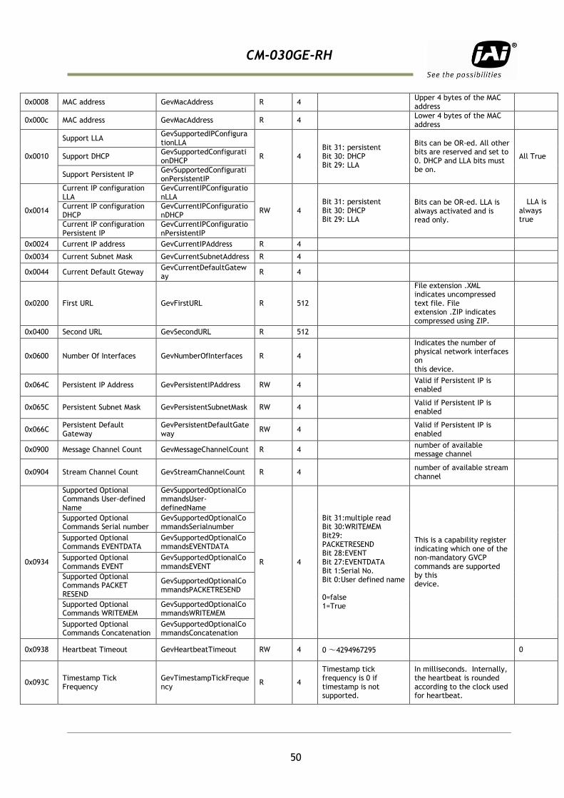
Register Map
The table below provides detailed information for the hardware registers used for controlling the camera and obtaining information on the status of the camera. The content of this register map is also found in the XML file, as stipulated by the GenICam standard.
Image Format Control
Address Display Name (JAI Control Tool)
GenICam name Read / Write
Size Value / Range of value Description Default value
0xA400 Width Max WidthMax R 4 656 Width max 1024
0xA404 Height Max HeightMax R 4 494 Height max 768
0xA410 Pixel Format PixelFormat
RW
4
0x01080001 0x010C0004 0x01100003
Mono8 Mono10Packed Mono10
Mono8
0xA500 ROI Mode ROIMode
RW
4 1 to 5 1:ROI disable 2 to 5: Enable
0xA500
0xA504 ROI 1 Width Width RW
4 8 - 656 Width W.Max
0xA508 ROI 1 Height Height RW
4 8 – 494 Height H.Max
0xA50C ROI 1 Offset X OffsetX RW
4 0 – 648 Horizontal offset 0
0xA510 ROI 1 Offset Y OffsetY RW
4 0 – 486 Vertical offset 0
0xA514 ROI 2 Width Width2 RW
4 8 - 656 Width 2 W.Max
0xA518 ROI 2 Height Height2 RW
4 8 – 494 Height 2 H.Max
0xA51C ROI 2 Offset X OffsetX2 RW
4 0 – 648 Offset X2 0
0xA520 ROI 2 Offset Y OffsetY2 RW
4 0 – 486 Offset Y2 0
0xA524 ROI 3 Width Width3 RW
4 8 - 656 Width 3 W.Max
Device Information
Address Display Name (JAI Control Tool)
GenICam name Read / Write
Size Value / Range of value Description Default value
0x0048 Device Vendor Name DeviceVendoeName R 32 Manufacture of this device
0x0068 Device Model Name DeviceModelName R 32 Model Name of this device
0x0088 Device Version DeviceVersion R 32 Version of this device
0x00A8 Device Manufacturer Info
DeviceManufacturerInfo R 48 Provides extended manufacturer information about the device.
0x00D8 Device ID DeviceID R 16 Camera serial number
0x00E8 Device User ID DeviceUserID RW 16 User assignable string (16 Byte)
0xA714 FPGA version DeviceFPGAVersion R 4
0xA640 Device Reset DeviceReset W 4 Command=1

CM-030GE-RH
46
0xA528 ROI 3 Height Height3 RW
4 8 – 494 Height 3 H.Max
0xA52C ROI 3 Offset X OffsetX3 RW
4 0 – 648 Offset X3 0
0xA530 ROI 3 Offset Y OffsetY3 RW
4 0 – 486 Offset Y3 0
0xA534 ROI 4 Width Width4 RW
4 8 - 656 Width 4 W.Max
0xA538 ROI 4 Height Height4 RW
4 8 – 494 Height 4 H.Max
0xA53C ROI 4 Offset X OffsetX4 RW
4 0 – 648 Offset X4 0
0xA540 ROI 4 Offset Y OffsetY4 RW
4 0 – 486 Offset Y4 0
0xA544 ROI 5 Width Width5 RW
4 8 - 656 Width 5 W.Max
0xA548 ROI 5 Height Height5 RW
4 8 – 494 Height 2 H.Max
0xA54C ROI 5 Offset X OffsetX5 RW
4 0 – 648 Offset X 5 0
0xA550 ROI 5 Offset Y OffsetY5 RW
4 0 – 486 Offset Y 5 0
0xA080 Fast Dump FastDumpEnable RW 4 For enabling variable partial scan
0xA084 Binning Vertical BinningVertical RW 4 1=Binning OFF 2=1/2 V Binning
1
0xA098 Sync Mode SyncMode RW 4 0=Sync 1=Async
0xA13C Test Image Selector TestImageSeleector RW 4
0=OFF 1=White Noise 4=H Rmap Scale 5=V Ramp Scale 6= Moving Ramp Scale
0
0xA41C OB Transfer Enable OBTransferEnable RW 4
Acquisition and Trigger Control
Address Display Name (JAI Control Tool)
GenICam name Read / Write
Size Value / Range of value Description Default value
0xA604 Acquisition Mode AcquisitionMode RW
4 0=Stop 1=Start Acquisition start and stop 0
0xA414 Acquisition frame rate AcquisitionFrameRate
RW
4
0=Full speed 1=1/2 speed 2=1/4 speed 3=1/8 speed
0
0xA000 Shutter mode ShutterMode RW 4
1= Programmable exposure in line 2=Programmable exposure(us) 3=Auto Exposure Constantly
Sets exposure time for image capture.
1
0xA004 Preset Shutter PresetShutter RW 4
0=OFF 1=1/250 2=1/500 3=1/1000 4=1/2000 5=1/4000 6=1/8000 7=1/10000 8=1/15000 9=1/30000
0
0xA008 Exposure Time Raw ExposureTimeRaw RW 4 0 to 511 (OFF)
Flexible setting of exposure time ranging from 32.5 µs
511

CM-030GE-RH
47
to 8.299 ms using the LVAL period (L) as increment. 1L is 16.24us.
0xA018 Exposure Time (us) ExposureTimeAbs RW 4 32 to 8307 ( OFF)
Actual exposure time in microseconds, µs. The camera will round value off to match LVAL increments.
33333
0xA040 Exposure Mode ExposureMode RW 4
00=Continuous trigger 01=Edge pre-select 02=Pulse-width control
09=Sequential EPS trigger 17=Delayed readout EPS trigger 18=Delayed readout PWC trigger
0
Analog Control
Address Display Name (JAI Control Tool)
GenICam name Read / Write
Size Value / Range of value Description Default value
0xA0C4 Gain Raw GainRaw RW 4 -89 to 341 Value 0=0dB 0
0xA0E0 Black Level in Raw Format
BlackLevelRaw
RW 4 0 ~ 1024
Group name : Digital IO
Address Display Name (JAI Control Tool)
GenICam name Read / Write
Size Value / Range of value Description Default value
0xA600 Soft trigger 0 SoftTrigger0 WO 4 0=Low 1=HIGH 0
0xA644 Soft trigger 1 SoftTrigger1 WO 4 0=Low 1=HIGH 0
0xA648 Soft trigger 2 SoftTrigger2 WO 4 0=Low 1=HIGH 0
0xA64C Soft trigger 3 SoftTrigger3 WO 4 0=Low 1=HIGH 0
0xB060 Camera trigger 0 CameraTrigger0 RW 4
0xB064 Camera trigger 1 CameraTrigger 1 RW 4
0xB070 GPIO Port 1 (Optical Out 1)
GPIO_Port1 RW 4 Line Source Bit31 ~ Bit25 Bit24:Line Inverter 0=False (Active High) 1=True(Active Low)
Line Source 127:OFF 0:LVAL 1:DVAL 2:FVAL 3:EEN 4:GPIO Port In 1(Optical In 1) 5:GPIO Port In 2(Optical In 2) 12:Software Trigger 0 13:Software Trigger 1 14:Software Trigger 2 15:Software Trigger 3 16:Pulse Generator 0 17:Pulse Generator 1 18:Pulse Generator 2 19:Pulse Generator 3
0xB078 GPIO Port 2 (Optical Out 2)
GPIO_Port2 RW 4
0xB090 Pulse Generator 0 PulseGenerator0 RW 4
0xB094 Pulse Generator 1 PulseGenerator1 RW 4
0xB098 Pulse Generator 2 PulseGenerator2 RW 4
0xB09C Pulse Generator 3 PulseGenerator3 RW 4
0xB0A0 TimeStamp Reset TimeStampReset RW 4
Pulse Generator
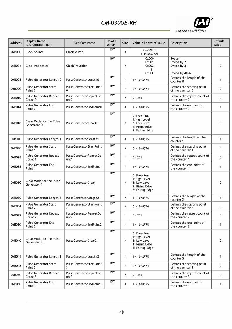
CM-030GE-RH
48
Address Display Name (JAI Control Tool)
GenICam name Read / Write
Size Value / Range of value Description Default value
0xB000 Clock Source ClockSource RW
4 0=25MHz
1=PixelClock
0xB004 Clock Pre-scaler ClockPreScaler
RW
4
0x000 0x001 0x002 |
0xFFF
Bypass Divide by 2 Divide by 3 | Divide by 4096
0
0xB008 Pulse Generator Length 0 PulseGeneratorLength0 RW
4 1~1048575 Defines the length of the counter 0
1
0xB00C Pulse Generator Start Point 0
PulseGeneratorStartPoint0
RW 4 0~1048574
Defines the starting point of the counter 0
0
0xB010 Pulse Generator Repeat Count 0
PulseGeneratorRepeatCount0
RW 4 0 - 255
Defines the repeat count of the counter 0
0
0xB014 Pulse Generator End Point 0
PulseGeneratorEndPoint0 RW
4 1~1048575 Defines the end point of the counter 0
1
0xB018 Clear Mode for the Pulse Generator 0
PulseGeneratorClear0
RW
4
0 :Free Run 1:High Level 2: Low Level 4: Rising Edge 8: Falling Edge
0
0xB01C Pulse Generator Length 1 PulseGeneratorLength1 RW
4 1~1048575 Defines the length of the counter 1
1
0xB020 Pulse Generator Start Point 1
PulseGeneratorStartPoint1
RW 4 0~1048574
Defines the starting point of the counter 1
0
0xB024 Pulse Generator Repeat Count 1
PulseGeneratorRepeatCount1
RW 4 0 - 255
Defines the repeat count of the counter 1
0
0xB028 Pulse Generator End Point 1
PulseGeneratorEndPoint1 RW
4 1~1048575 Defines the end point of the counter 1
1
0xB02C Clear Mode for the Pulse Generator 1
PulseGeneratorClear1
RW
4
0 :Free Run 1:High Level 2: Low Level 4: Rising Edge 8: Falling Edge
0
0xB030 Pulse Generator Length 2 PulseGeneratorLength2 RW
4 1~1048575 Defines the length of the counter 2
1
0xB034 Pulse Generator Start Point 2
PulseGeneratorStartPoint2
RW 4 0~1048574
Defines the starting point of the counter 2
0
0xB038 Pulse Generator Repeat Count 2
PulseGeneratorRepeatCount2
RW 4 0 - 255
Defines the repeat count of the counter 2
0
0xB03C Pulse Generator End Point 2
PulseGeneratorEndPoint2 RW
4 1~1048575 Defines the end point of the counter 2
1
0xB040 Clear Mode for the Pulse Generator 2
PulseGeneratorClear2
RW
4
0 :Free Run 1:High Level 2: Low Level 4: Rising Edge 8: Falling Edge
0
0xB044 Pulse Generator Length 3 PulseGeneratorLength3 RW
4 1~1048575 Defines the length of the counter 3
1
0xB048 Pulse Generator Start Point 3
PulseGeneratorStartPoint3
RW 4 0~1048574
Defines the starting point of the counter 3
0
0xB04C Pulse Generator Repeat Count 3
PulseGeneratorRepeatCount3
RW 4 0 - 255
Defines the repeat count of the counter 3
0
0xB050 Pulse Generator End Point 3
PulseGeneratorEndPoint3 RW
4 1~1048575 Defines the end point of the counter 3
1
CM-030GE-RH
49
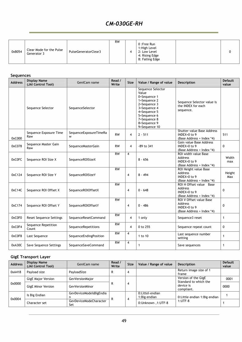
0xB054 Clear Mode for the Pulse Generator 3
PulseGeneratorClear3
RW
4
0 :Free Run 1:High Level 2: Low Level 4: Rising Edge 8: Falling Edge
0
Sequences
Address Display Name (JAI Control Tool)
GenICam name Read / Write
Size Value / Range of value Description Default value
Sequence Selector SequenceSelector
Sequence Selector Value 0=Sequence 1 1=Sequence 2 2=Sequence 3 3=Sequence 4 4=Sequence 5 5=Sequence 6 7=Sequence 8 8=Sequence 9 9=Sequence 10
Sequence Selector value is the INDEX for each
sequence。
0xC000
Sequence Exposure Time Raw
SequenceExposureTimeRaw
RW 4 2 - 511 Shutter value Base Address INDEX=0 to 9 (Base Address + Index *4)
511
0xC078 Sequence Master Gain Raw
SequenceMasterGain RW 4 -89 to 341 Gain value Base Address INDEX=0 to 9 (Base Address + Index *4)
0
0xC0FC Sequence ROI Size X SequenceROISizeX
RW 4
8 - 656
ROI width value Base Address INDEX=0 to 9 (Base Address + Index *4)
Width max
0xC124 Sequence ROI Size Y SequenceROISizeY
RW
4 8 - 494
ROI Height value Base Address INDEX=0 to 9 (Base Address + Index *4)
Height Max
0xC14C Sequence ROI Offset X SequenceROIOffsetX
RW
4 0 - 648
ROI H Offset value Base Address INDEX=0 to 9 (Base Address + Index *4)
0
0xC174 Sequence ROI Offset Y SequenceROIOffsetY
RW
4 0 - 486
ROI V Offset value Base Address INDEX=0 to 9 (Base Address + Index *4)
0
0xC0F0 Reset Sequence Settings SequenceResetCommand RW
4 1 only Sequence3 reset 1
0xC0F4 Sequence Repetition Count
SequenceRepetitions RW
4 0 to 255 Sequence repeat count 0
0xC0F8 Last Sequence SequenceEndingPosition RW 4
1 to 10 Last sequence number setting
1
0xA30C Save Sequence Settings SequenceSaveCommand RW 4
1 Save sequences 1
GigE Transport Layer
Address Display Name (JAI Control Tool)
GenICam name Read / Write
Size Value / Range of value Description Default value
0xA418 Payload size PayloadSize R 4 Return image size of 1 frame
0x0000
GigE Major Version GevVersionMajor
R 4
Version of the GigE Standard to which the device is compliant.
0001
GigE Minor Version GevVersionMinor 0000
0x0004
Is Big Endian GevDeviceModeIsBigEndian
R 4
0:Littel-endian 1:Big-endian 0:Little endian 1:Big endian
1:UTF-8
1
Character set GevDeviceModeCharacterSet
0:Unknown ,1:UTF-8 1
CM-030GE-RH
50
0x0008 MAC address GevMacAddress R 4 Upper 4 bytes of the MAC address
0x000c MAC address GevMacAddress R 4 Lower 4 bytes of the MAC address
0x0010
Support LLA GevSupportedIPConfigurationLLA
R 4 Bit 31: persistent Bit 30: DHCP Bit 29: LLA
Bits can be OR-ed. All other bits are reserved and set to 0. DHCP and LLA bits must be on.
All True Support DHCP GevSupportedConfigurationDHCP
Support Persistent IP GevSupportedConfigurationPersistentIP
0x0014
Current IP configuration LLA
GevCurrentIPConfigurationLLA
RW 4 Bit 31: persistent Bit 30: DHCP Bit 29: LLA
Bits can be OR-ed. LLA is always activated and is read only.
LLA is always true
Current IP configuration DHCP
GevCurrentIPConfigurationDHCP
Current IP configuration Persistent IP
GevCurrentIPConfigurationPersistentIP
0x0024 Current IP address GevCurrentIPAddress R 4
0x0034 Current Subnet Mask GevCurrentSubnetAddress R 4
0x0044 Current Default Gteway GevCurrentDefaultGateway
R 4
0x0200 First URL GevFirstURL R 512
File extension .XML indicates uncompressed text file. File extension .ZIP indicates compressed using ZIP.
0x0400 Second URL GevSecondURL R 512
0x0600 Number Of Interfaces GevNumberOfInterfaces R 4
Indicates the number of physical network interfaces on this device.
0x064C Persistent IP Address GevPersistentIPAddress RW 4 Valid if Persistent IP is enabled
0x065C Persistent Subnet Mask GevPersistentSubnetMask RW 4 Valid if Persistent IP is enabled
0x066C Persistent Default Gateway
GevPersistentDefaultGateway
RW 4 Valid if Persistent IP is enabled
0x0900 Message Channel Count GevMessageChannelCount R 4 number of available message channel
0x0904 Stream Channel Count GevStreamChannelCount R 4 number of available stream channel
0x0934
Supported Optional Commands User-defined Name
GevSupportedOptionalCommandsUser-definedName
R 4
Bit 31:multiple read Bit 30:WRITEMEM Bit29: PACKETRESEND Bit 28:EVENT Bit 27:EVENTDATA Bit 1:Serial No. Bit 0:User defined name 0=false 1=True
This is a capability register indicating which one of the non-mandatory GVCP commands are supported by this device.
Supported Optional Commands Serial number
GevSupportedOptionalCommandsSerialnumber
Supported Optional Commands EVENTDATA
GevSupportedOptionalCommandsEVENTDATA
Supported Optional Commands EVENT
GevSupportedOptionalCommandsEVENT
Supported Optional Commands PACKET RESEND
GevSupportedOptionalCommandsPACKETRESEND
Supported Optional Commands WRITEMEM
GevSupportedOptionalCommandsWRITEMEM
Supported Optional Commands Concatenation
GevSupportedOptionalCommandsConcatenation
0x0938 Heartbeat Timeout GevHeartbeatTimeout RW 4 0 ~4294967295 0
0x093C Timestamp Tick Frequency
GevTimestampTickFrequency
R 4
Timestamp tick frequency is 0 if timestamp is not supported.
In milliseconds. Internally, the heartbeat is rounded according to the clock used for heartbeat.

CM-030GE-RH
51
0x0940 GevTimestampTickFrequency
R 4
64-bit value indicating the number of timestamp clock ticks in 1 second. This register holds the most significant bytes.
0x0944
Timestamp control Latch GevTimestampcontrolLatch
W 4
Command 2 This register holds the least significant bytes. Used to latch the current timestamp value. No need to clear to 0.
Timestamp control Reset GevTimestampcontrolReset
Command 1
0x0948
Timestamp Tick Value
GevTimeStampValue R 4 High Latched value of the timestamp (most significant bytes)
0x094C GevTimeStampValue R 4 Low Latched value of the timestamp (least significant bytes)
0x0A00 Control Channel Privilege Feature
GevCCP R 4
0:Open Access 1:Exclusive 2:Control 3:Exclusive Control
control channel privilege register
0
0x0B00 Message Channel Port GevMCPHostPort R 4 message channel port
register 0
0x0B10 Message Channel Destination Address
GevMCDA R 4 message channel
destination address register
0x0B14 Message Channel Transmission Timeout
GevMCTT R 4 message channel transfer
timeout: ms 300
0x0B18 Message Channel Retry Count
GevMCRC R 4 message channel retry
count 2
0x0D00 Stream Channel Port GevSCPHostPort R 4 primary stream port
register
0x0D04
Packet Size GevSCPSPacketSize
RW 4
1476 ~16020
primary stream channel packet size register/ packet size includes IP, UDP&GVSP Header
1476
Do Not Fragment GevSCPSDoNotFragment 0=False 1=True
This bit is copied into the ”don’t fragment Ebit of IP header of each stream packet. It can be used by the application to prevent IP fragmentation of packets on the stream channel.
1
0x0D08 Packet Delay GevSCPD RW 4 0 ~ 125000 Set the delay in between packets
0
0x0D18 Strem Channel Destination Address
GevSCDA R 4 primary stream channel
destination address register
Event Generation
Address Display Name (JAI Control Tool)
GenICam name Read / Write
Size Value / Range of value Description Default value

CM-030GE-RH
52
0xA610
Event Selector Acquisition Trigger
GevEventtreigger
RW
4
Selector Value 0
Event message ON/OFF
0
Exposure Start GevEventStartOfExposure 1 0
Exposure End GevEventEndOfExposure 2 0
Frame Transfer Start GevEventStartOfTransfer 3 0
Frame Transfer End GevEventEndOfTransfer 4 0
Event Notification EventNotification 0=Disable 1=Enable
User Sets
Address Display Name (JAI Control Tool)
GenICam name Read / Write
Size Value / Range of value Description Default value
0xA300 UserSet Save UserSetSave W 4 1=User area1
Allows use to save all camera settings. Last used area number becomes new default.
1
0xA304 UserSet Load UserSetLoad W 4 0=Factory area 1=User area1
Allow the user to recall all camera settings.
0
0xA308 UserSet Selector UserSetSelector RW 4
Whenreceiving following commands,store the parameters 0xA300 0xA304
Check the used data, 0=Factory or1=User
0

CM-030GE-RH
53
Appendix
1. Precautions
Personnel not trained in dealing with similar electronic devices should not service this camera. The camera contains components sensitive to electrostatic discharge. The handling of these devices should follow the requirements of electrostatic sensitive components. Do not attempt to disassemble this camera. Do not expose this camera to rain or moisture. Do not face this camera towards the sun, extreme bright light or light reflecting objects. When this camera is not in use, put the supplied lens cap on the lens mount. Handle this camera with the maximum care. Operate this camera only from the type of power source indicated on the camera. Remove power from the camera during any modification work, such as changes of jumper and switch settings.
2. Typical Sensor Characteristics
The following effects may be observed on the video monitor screen. They do not indicate any fault of the camera, but are associated with typical sensor characteristics. V. Aliasing When the camera captures stripes, straight lines or similar sharp patterns, a jagged image on the monitor may appear. Blemishes All cameras are shipped without visible image sensor blemishes. Over time some pixel defects can occur. This does not have a practical effect on the operation of the camera. These will show up as white spots (blemishes). Exposure to cosmic rays can cause blemishes to appear on the image sensor. Please take care to avoid exposure to cosmic rays during transportation and storage. It is recommended using sea shipment instead of air flight in order to limit the influence of cosmic rays on the camera. Pixel defects/blemishes also may emerge due to prolonged operation at elevated ambient temperature, due to high gain setting or during long time exposure. It is therefore recommended to operate the camera within its specifications. Patterned Noise When the sensor captures a dark object at high temperature or is used for long time integration, fixed pattern noise may appear in the image.
3. Caution when mounting a lens on the camera
When mounting a lens on the camera dust particles in the air may settle on the surface of the lens or the image sensor of the camera. It is therefore important to keep the protective caps on the lens and on the camera until the lens is mounted. Point the lens mount of the camera downward to prevent dust particles from landing on the optical surfaces of the camera. This work should be done in a dust free environment. Do not touch any of the optical surfaces of the camera or the lens.
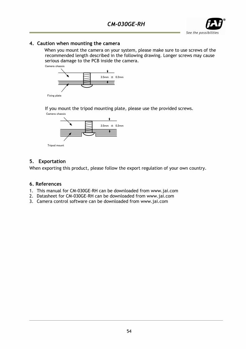
CM-030GE-RH
54
4. Caution when mounting the camera
When you mount the camera on your system, please make sure to use screws of the recommended length described in the following drawing. Longer screws may cause serious damage to the PCB inside the camera.
If you mount the tripod mounting plate, please use the provided screws.
5. Exportation
When exporting this product, please follow the export regulation of your own country.
6. References
1. This manual for CM-030GE-RH can be downloaded from www.jai.com 2. Datasheet for CM-030GE-RH can be downloaded from www.jai.com 3. Camera control software can be downloaded from www.jai.com
Camera chassis
Fixing plate
3.5mm ± 0.2mm
Camera chassis
Tripod mount
3.5mm ± 0.2mm
CM-030GE-RH
55
Index
A
asynchronous, 4, 11, 17, 19, 33
B
Bayer mosaic color, 4
Binning mode, 12
Bit Allocation, 9, 26
Black Level, 26
Blemishes, 34
C
Camera Control Tool, 4, 27, 28, 29, 30
Camera Link, 5, 6, 9, 11, 18, 20, 23, 25, 28, 33
CCD sensor, 5, 13, 24, 33, 35
Continuous operation, 4, 9, 11, 17
D
Digital Output, 6, 9
E
EPS with Smear Less trigger mode, 21
external trigger, 11, 17, 18
External trigger, 4
G
Gain, 24, 26, 33
Gamma, 33
H
Hirose, 18, 20, 25
I
indicator, 11
L
Lens mount, 33
LVAL synchronous, 11, 33
O
OCX, 27
P
Partial Scan, 15
Partial scanning, 9, 15, 16, 24
Pixels in video output, 33
PoCL, 4, 6
Power over Mini-CL, 4
Pre-select Trigger Mode, 18
Preset Shutter, 10, 25, 33
programmable exposure, 10
Programmable exposure, 4, 25, 33
Programmable Exposure, 10
Progressive scan, 4
Pulse Width, 4, 9, 17, 20, 21, 33
R
rear panel mounted LED, 11
reset feed trough, 11
S
Scanning format, 24
Spectral response, 32
Synchronization, 33
T
Trigger input, 5, 11
Trigger polarity, 24
V
Vertical Binning, 12, 16, 17

CM-030GE-RH
56
Change History Month/Year Revision Changes
Dec2009 1.0 New release
March 2011 1.1 Delete Register 0xA1FC temperature because this is not implemented.

CM-030GE-RH
57
User's Record
Camera type: CM-030GE-RH Revision: …………….. Serial No. …………….. Firmware version. ……………..
For camera revision history, please contact your local JAI distributor.
User's Mode Settings. User's Modifications. Company and product names mentioned in this manual are trademarks or registered trademarks of their respective owners. JAI A-S cannot be held responsible for any technical or typographical errors and reserves the right to make changes to products and documentation without prior notification.
Europe, Middle East & Africa Asia Pacific Americas
Phone +45 4457 8888
Fax +45 4491 3252
Phone +81 45 440 0154
Fax +81 45 440 0166
Phone (toll-free) +1 800 445 5444
Phone +1 408 383 0300
Visit our web site at www.jai.com