Curriculum Vitae Sandip Tiwari - Cornell...
21
Sandip Tiwari 1 of 21 Curriculum Vitae Sandip Tiwari [email protected], 607.254.6254 Sandip Tiwari is the Charles N. Mellowes Professor in Engineering at Cornell University. His current research interests are in questions that arise when connecting large scales such as those of massively integrated electronic systems to small scales. In pursuit of answers, his group has developed ideas in adaptive electronics, small devices and their circuits, and three-dimensional and functional integration. His widely cited experimental and theoretical contributions span electronic and optical devices and circuits. Among his contributions and inventions of note have been nanocrystal memories, back-side trapping memories, architectures and technologies of three-dimensional integration, and the early investigations of III-V and SiGe heterostructure bipolar transistors and their technologies. His theoretical efforts have provided the fundamental understanding of several device phenomena including the electron injection processes in coupled confined systems, frequency limitations of quantum-wire lasers due to gain compression, and surface recombination and injection and collection effects at high currents in heterostructure bipolar transistors. He is a frequent keynote and invited speaker at major conferences summarizing learning and articulating new themes, technical directions and their needs. His current efforts also include the societal, particularly the international, view of technology and the context of poverty, food, health and water. Prior to joining Cornell in 1999, Sandip Tiwari was a Research Staff Member and Manager for Exploratory Devices and Device Modeling at IBM Thomas J. Watson Research Center. He has held visiting and adjunct faculty appointments at the University of Michigan (1988-89), Columbia University (1993) and Harvard University (2005-06). He is a Fellow of Institution of Electronic and Electrical Engineers (1994; for contributions to heterostructure devices) and American Physical Society (1998; for contributions to understanding of device physics and for innovations in small electronic and optical devices with strong quantum confinement). He received the Young Scientist Award of 1991 from Institute of Physics at the 18’th International Symposium on GaAs and Related Compounds for contributions to the understanding and development of the metal-semiconductor field-effect transistor, the heterostructure field-effect transistor and the heterostructure bipolar transistor; the Distinguished Alumnus Award of 2003 from IIT- Kanpur for contributions in microelectronics and nanofabrication technologies; and the 2007 IEEE Brunetti Award for nanocrystal memory and quantum-effect devices. IBM recognized his scientific achievements with Outstanding Research Contribution (1991) and Outstanding Technical Contribution (1987, 1989) awards. He serves on the Defense Sciences Research Council, National Advisory Committee of the University of Michigan Department of Electrical Engineering and Computer Sciences, and on the Technical Activities Board of Samsung Electronics, Anvik Corp and ADC Inc. He is the founding Editor-in-Chief of IEEE Transactions on Nanotechnology, a past Associate Editor and Guest Editor of IEEE Trans. on Electron Devices, and past Chair of many conferences and workshops. He is also the author of a widely used graduate text-book “Compound Semiconductor Device Physics” published by Academic Press, and holds many patents. His passion for teaching is reflected in a number of new courses that he has developed for advanced electrosciences-centered curriculum at Cornell. Sandip Tiwari was educated at Indian Institute of Technology at Kanpur (B. Tech. in Electrical Engineering, 1976), Rensselaer Polytechnic Institute (M. Eng. in Electrical & Systems Engineering, 1977) and Cornell University (Ph.D. in Electrical Engineeing, 1980). His college education was supported through fellowships (National Science Talent Scholarship and Shreedhar Memorial Scholarship for undergraduate education, and General Electric Fellowship for graduate education). He has served as Lester B. Knight Director of Cornell Nanoscale Science and Technology Facility (1999- 2005), director of National Nanofabrication Users Network (2000-2003), and currently serves as director of the National Nanotechnology Infrastructure Network (2004-). NNIN is a many university partnership funded by National Science Foundation (currently $14M/year) to enable research in nanoscale science, engineering and technology and to conduct international, national and local outreach.
Transcript of Curriculum Vitae Sandip Tiwari - Cornell...
Sandip Tiwari 1 of 21
Curriculum Vitae Sandip Tiwari
[email protected], 607.254.6254 Sandip Tiwari is the Charles N. Mellowes Professor in Engineering at Cornell University. His current research interests are in questions that arise when connecting large scales such as those of massively integrated electronic systems to small scales. In pursuit of answers, his group has developed ideas in adaptive electronics, small devices and their circuits, and three-dimensional and functional integration.
His widely cited experimental and theoretical contributions span electronic and optical devices and circuits. Among his contributions and inventions of note have been nanocrystal memories, back-side trapping memories, architectures and technologies of three-dimensional integration, and the early investigations of III-V and SiGe heterostructure bipolar transistors and their technologies. His theoretical efforts have provided the fundamental understanding of several device phenomena including the electron injection processes in coupled confined systems, frequency limitations of quantum-wire lasers due to gain compression, and surface recombination and injection and collection effects at high currents in heterostructure bipolar transistors. He is a frequent keynote and invited speaker at major conferences summarizing learning and articulating new themes, technical directions and their needs. His current efforts also include the societal, particularly the international, view of technology and the context of poverty, food, health and water.
Prior to joining Cornell in 1999, Sandip Tiwari was a Research Staff Member and Manager for Exploratory Devices and Device Modeling at IBM Thomas J. Watson Research Center. He has held visiting and adjunct faculty appointments at the University of Michigan (1988-89), Columbia University (1993) and Harvard University (2005-06). He is a Fellow of Institution of Electronic and Electrical Engineers (1994; for contributions to heterostructure devices) and American Physical Society (1998; for contributions to understanding of device physics and for innovations in small electronic and optical devices with strong quantum confinement). He received the Young Scientist Award of 1991 from Institute of Physics at the 18’th International Symposium on GaAs and Related Compounds for contributions to the understanding and development of the metal-semiconductor field-effect transistor, the heterostructure field-effect transistor and the heterostructure bipolar transistor; the Distinguished Alumnus Award of 2003 from IIT-Kanpur for contributions in microelectronics and nanofabrication technologies; and the 2007 IEEE Brunetti Award for nanocrystal memory and quantum-effect devices. IBM recognized his scientific achievements with Outstanding Research Contribution (1991) and Outstanding Technical Contribution (1987, 1989) awards.
He serves on the Defense Sciences Research Council, National Advisory Committee of the University of Michigan Department of Electrical Engineering and Computer Sciences, and on the Technical Activities Board of Samsung Electronics, Anvik Corp and ADC Inc. He is the founding Editor-in-Chief of IEEE Transactions on Nanotechnology, a past Associate Editor and Guest Editor of IEEE Trans. on Electron Devices, and past Chair of many conferences and workshops. He is also the author of a widely used graduate text-book “Compound Semiconductor Device Physics” published by Academic Press, and holds many patents. His passion for teaching is reflected in a number of new courses that he has developed for advanced electrosciences-centered curriculum at Cornell.
Sandip Tiwari was educated at Indian Institute of Technology at Kanpur (B. Tech. in Electrical Engineering, 1976), Rensselaer Polytechnic Institute (M. Eng. in Electrical & Systems Engineering, 1977) and Cornell University (Ph.D. in Electrical Engineeing, 1980). His college education was supported through fellowships (National Science Talent Scholarship and Shreedhar Memorial Scholarship for undergraduate education, and General Electric Fellowship for graduate education).
He has served as Lester B. Knight Director of Cornell Nanoscale Science and Technology Facility (1999-2005), director of National Nanofabrication Users Network (2000-2003), and currently serves as director of the National Nanotechnology Infrastructure Network (2004-). NNIN is a many university partnership funded by National Science Foundation (currently $14M/year) to enable research in nanoscale science, engineering and technology and to conduct international, national and local outreach.
Sandip Tiwari 2 of 21
Curriculum Vitae
Sandip Tiwari [email protected]
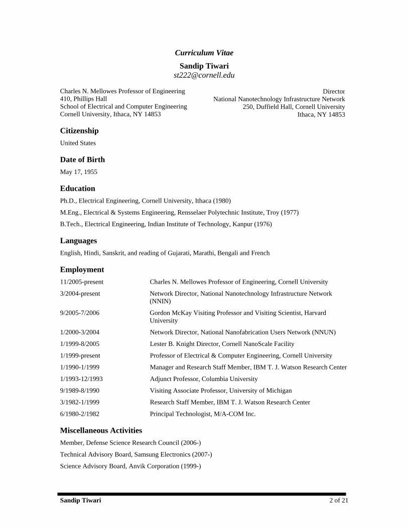
Charles N. Mellowes Professor of Engineering 410, Phillips Hall School of Electrical and Computer Engineering Cornell University, Ithaca, NY 14853
Citizenship United States
Date of Birth May 17, 1955
Education Ph.D., Electrical Engineering, Cornell University, Ithaca (1980)
M.Eng., Electrical & Systems Engineering, Rensselaer Polytechnic Institute, Troy (1977)
B.Tech., Electrical Engineering, Indian Institute of Technology, Kanpur (1976)
Languages English, Hindi, Sanskrit, and reading of Gujarati, Marathi, Bengali and French
Employment 11/2005-present Charles N. Mellowes Professor of Engineering, Cornell University
3/2004-present Network Director, National Nanotechnology Infrastructure Network (NNIN)
9/2005-7/2006 Gordon McKay Visiting Professor and Visiting Scientist, Harvard University
1/2000-3/2004 Network Director, National Nanofabrication Users Network (NNUN)
1/1999-8/2005 Lester B. Knight Director, Cornell NanoScale Facility
1/1999-present Professor of Electrical & Computer Engineering, Cornell University
1/1990-1/1999 Manager and Research Staff Member, IBM T. J. Watson Research Center
1/1993-12/1993 Adjunct Professor, Columbia University
9/1989-8/1990 Visiting Associate Professor, University of Michigan
3/1982-1/1999 Research Staff Member, IBM T. J. Watson Research Center
6/1980-2/1982 Principal Technologist, M/A-COM Inc.
Miscellaneous Activities Member, Defense Science Research Council (2006-)
Technical Advisory Board, Samsung Electronics (2007-)
Science Advisory Board, Anvik Corporation (1999-)
DirectorNational Nanotechnology Infrastructure Network
250, Duffield Hall, Cornell UniversityIthaca, NY 14853
Sandip Tiwari 3 of 21
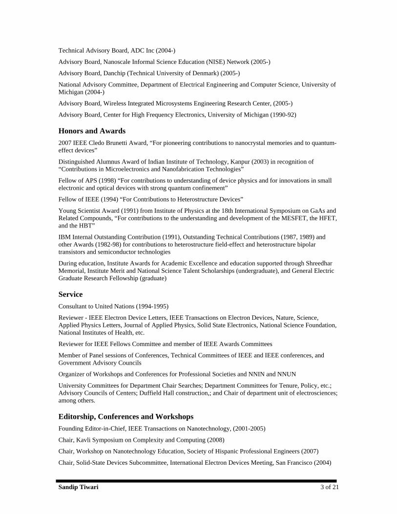
Technical Advisory Board, ADC Inc (2004-)
Advisory Board, Nanoscale Informal Science Education (NISE) Network (2005-)
Advisory Board, Danchip (Technical University of Denmark) (2005-)
National Advisory Committee, Department of Electrical Engineering and Computer Science, University of Michigan (2004-)
Advisory Board, Wireless Integrated Microsystems Engineering Research Center, (2005-)
Advisory Board, Center for High Frequency Electronics, University of Michigan (1990-92)
Honors and Awards 2007 IEEE Cledo Brunetti Award, “For pioneering contributions to nanocrystal memories and to quantum-effect devices”
Distinguished Alumnus Award of Indian Institute of Technology, Kanpur (2003) in recognition of “Contributions in Microelectronics and Nanofabrication Technologies”
Fellow of APS (1998) “For contributions to understanding of device physics and for innovations in small electronic and optical devices with strong quantum confinement”
Fellow of IEEE (1994) “For Contributions to Heterostructure Devices”
Young Scientist Award (1991) from Institute of Physics at the 18th International Symposium on GaAs and Related Compounds, “For contributions to the understanding and development of the MESFET, the HFET, and the HBT”
IBM Internal Outstanding Contribution (1991), Outstanding Technical Contributions (1987, 1989) and other Awards (1982-98) for contributions to heterostructure field-effect and heterostructure bipolar transistors and semiconductor technologies
During education, Institute Awards for Academic Excellence and education supported through Shreedhar Memorial, Institute Merit and National Science Talent Scholarships (undergraduate), and General Electric Graduate Research Fellowship (graduate)
Service Consultant to United Nations (1994-1995)
Reviewer - IEEE Electron Device Letters, IEEE Transactions on Electron Devices, Nature, Science, Applied Physics Letters, Journal of Applied Physics, Solid State Electronics, National Science Foundation, National Institutes of Health, etc.
Reviewer for IEEE Fellows Committee and member of IEEE Awards Committees
Member of Panel sessions of Conferences, Technical Committees of IEEE and IEEE conferences, and Government Advisory Councils
Organizer of Workshops and Conferences for Professional Societies and NNIN and NNUN
University Committees for Department Chair Searches; Department Committees for Tenure, Policy, etc.; Advisory Councils of Centers; Duffield Hall construction,; and Chair of department unit of electrosciences; among others.
Editorship, Conferences and Workshops Founding Editor-in-Chief, IEEE Transactions on Nanotechnology, (2001-2005)
Chair, Kavli Symposium on Complexity and Computing (2008)
Chair, Workshop on Nanotechnology Education, Society of Hispanic Professional Engineers (2007)
Chair, Solid-State Devices Subcommittee, International Electron Devices Meeting, San Francisco (2004)

Sandip Tiwari 4 of 21
Chair, NSF Workshop on Environmental Health and Safety in Nanotechnology Research (2004)
Chair, US-India Workshop on Educational Issues of Nanotechnology, Bangalore (2004)
Chair, US-Japan Symposium on Tools and Metrology for Nanotechnology, Ithaca (2003)
Co-Organizer, MRS Symposium on Materials Issues in Novel Si-Based Technology, Boston (2001)
Chair, US-India Workshop on Nanotechnology, Santa Barbara (2001)
Chair, IEEE Silicon Nanoelectronics Workshop, Waikiki (2000)
Chair, NSF/DARPA/NNUN Workshop on Chemical and Physical Nanotechnology, Washington (2000)
Associate Editor of IEEE Transactions on Electron Devices for III-V and Microwave Devices (1986-90)
Co-Guest Editor of Special Issue on Heterostructure Transistors of IEEE Transactions on Electron Devices (Oct. 1989)
Member of Technical Committees of IEEE, MRS and SPIE Conferences and Organizer of sessions
Keynote and Plenary Addresses NSTI Nanotech, Boston (2008)
Keck Nanotechnology Symposium, Howard University (2007)
Society of Hispanic Professional Engineers Nanotechnology Symposium (2007)
25th Microelectronic Engineering Conference (2007)
National Academy of Sciences Workshop on Condensed Matter and Materials Physics (2007)
20th International Conference on VLSI Design, Bangalore (2007)
IEEE Nanotechnology Materials and Devices Conference, Gyeongju (2006)
SPIE Photonics Europe, Strasbourg (2006)
IEEE Conference on Emerging Technologies – Nanoelectronics, Singapore (2006)
International Electron Devices and Materials Symposium, Tsin-Chu (2004)
SPIE Conf. on Microtechnologies for the New Millenium, Las Palamas (2003)
Next Generation Growth Engine of Future Industries, Seoul (2003)
Nano-7 and European Conference on Surface Science-21 (2002)
SEMI - South Korea, Seoul (2001)
IEEE Silicon Nanoelectronics Workshop, Kyoto (1999)
International Conference on Solid State Devices and Materials, Hiroshima (1998)
International Conference on Micro- and Nanofabrication, Leuven (1998)
IX’th European Workshop on Dielectrics in Microelectronics, Toulouse (1998)
Annual Meeting of Electrochemical Society, Boston (1998)
2nd International Symposium on Formation, Physics and Device Applications of Quantum Dot Structures, Hokkaido (1998)
European National Symposium on Nanometer Structures, Lund (1997)
3rd International Symposium on the Physics and Chemistry of SiO2 and the Si-SiO2 Interface, Electrochemical Society, May (1996)
Books
Sandip Tiwari 5 of 21
S. Tiwari, Compound Semiconductor Device Physics, Academic Press, Inc. (1992)
S. Tiwari, (Editor), Compound Semiconductor Transistors: Physics and Technology, IEEE Press (1993)
W.G. En, E. C. Jones, J.C. Sturm, M.J. Chan, S. Tiwari and M. Hirose (Editors), Materials Issues in Novel Si-Based Technology, Vol. 686, MRS Press (2001)
Book Chapters and Short Courses S. Tiwari, Compound Semiconductor HBTs: Device Physics, IEEE GaAs IC Symposium, Miami (1992)
S. Tiwari, High Speed Optoelectronic Elements, International Electron Devices and Materials Symposium Taipei (1992)
S. Tiwari, Silicon Memories Using Quantum and Single-Electron Effects, Book Chapter in Nanoelectronics, Ed. S. Oda and D. Ferry, Marcel Dekker (2006)
S. Tiwari, Potential, Characteristics and Issues of 3D SOI: 3D SOI Opportunities, IEEE Silicon on Insulators Conference (2005)
C. C. Liu and S. Tiwari, 3D Architectures and the Role of Interconnects, VLSI Multi-Level Interconnections Conference (2005)
S. Tiwari, Silicon Nanoelectronics: From Devices to Systems, IEEE Conference on Emerging Technologies – Nanoelectronics (2006)
S. Tiwari, Devices and Circuits of the Nanoscale, IEEE NMDC (2006)
Advisory Talks (2006 onwards) S. Tiwari, Hedgehogs, Foxes and Wolfpacks in Science and Engineering; You and Your Research (2008)
S. Tiwari, Terachip: Blank Slate Co-Design of Hardware, Software, Communication and Computation, to DARPA (2008)
S. Tiwari, Nanoscale Science and Engineering and our Place in the World, Keck Symposium (2007)
S. Tiwari, Nanoscale Technology: From Ideas in Laboratories to Useful Electronics and the Role of Complexity and Scales, to JASONS (2007)
S. Tiwari, Thermodynamics, Processing, Memories and Nanoscale: It is time to think, Samsung Board (2007)
S. Tiwari, Complexity and Energy: Experiments in Adaptation and Hierarchy in Electronics at Nanoscale, to Intel Corporation (2007)
S. Tiwari, Supporting Experimental Condensed Matter Science; the NNIN Experience, to National Academy of Sciences CMMP Committee (2007)
S. Tiwari, Past 25 Years and Next 25 Years in Electronics; Reality, Dreams and “MicroElectronics in a Changing World, to Microelectronic Engineering Conference (2007)
S. Tiwari, Nanoscale Science and Engineering: Undergraduate Education and Nanotechnology, to Society of Hispanic Professional Engineers (2007)
S. Tiwari, Experimental Usage and Diversity in Science and Engineering; the NNIN Experience, to National Science Foundation Facilities Meeting (2007)
S. Tiwari, Ultra-Low Power or, How to Achieve Efficiency by Reducing Energy Used?, to DARPA (2006)
S. Tiwari, Ultra-Low Power: The “Really” Intelligent Design Approach, DARPA (2006)
S. Tiwari, Nanotechnology and Nikon; An Academic’s Perspective, to Nikon Instrument Annual Meeting (2006)
Sandip Tiwari 6 of 21
S. Tiwari, Electronics at Nanoscale: Fundamental and Practical Challenges, and Emerging Directions, to University of West Indies (2006)
S. Tiwari, NNIN and Support of Research and Development, International Nanotechnology Conference 2 (2006)
S. Tiwari, Electronics at Nanoscale: Fundamental and Practical Challenges, and Emerging Directions, NSF-Korea Workshop (2006)
S. Tiwari, Grand Challenges of Nanoscale in Electronics, NanoFrontiers Workshop (2006)
S. Tiwari, Energy Constrained Limits to Operation and Assembly of Information Processing Systems: Lessons for Directions of Nanoscale Systems, NMDC Korea (2006)
S. Tiwari, Adaptive Electronics, to DARPA (2006)
Refereed Journal Publications S. Tiwari and S. Ashok, “A Simple Power Control Technique,” Electronics Letters, 14, No. 13, 393(1978)
R.J. Lender, S. Tiwari, J.M. Borrego, and S.K. Ghandhi, “Diffusion-Length Measurements in Schottky-Barrier GaAs Solar Cells,” Solid State Electronics, V22, No. 2, 213(1979)
K. Pande, D. Reep, A. Srivastava, S. Tiwari, J.M. Borrego, and S.K. Ghandhi, “Device Quality Polycrystalline Gallium Arsenide on Germanium/Molybdenum Substrates,” Journal of Electrochemical Society, V126, No. 2, 213(1979)
L.F. Eastman, S. Tiwari, and M.S. Shur, “Design Criteria for GaAs MESFETs Related to Stationary High Field Domains,” Solid State Electronics, V23, No. 4, 383(1980)
S. Tiwari, L.F. Eastman and L. Rathbun, “Physical and Materials Limitation on Burn-Out Voltage of GaAs Power MESFETs,” IEEE Transactions on Electron Devices, ED-27, No. 6, 1045(1980)
T.S. Low, G.E. Stillman, D.M. Collins, C.M. Wolfe, S. Tiwari, and L.F. Eastman, “Spectroscopic Identification of Si Donors in GaAs,” Applied Physics Letters, V40, No. 12, 1034(1982)
W. Camp and S. Tiwari, “A Quantum Jump: Gallium Arsenide Monolithic Microwave Circuits,” IBM Technical Directions, 9, No. 1, 27(1983)
S. Tiwari, “Threshold and Sheet Concentration Sensitivity of High Electron Mobility Transistors,” IEEE Transactions on Electron Devices, ED-31, No. 7, p. 879 (1984)
S. Tiwari and W.I. Wang, “p-channel MODFETs Using GaAlAs/GaAs Two-Dimensional Hole Gas,” IEEE Electron Device Letters, EDL-5, p. 333 (1984)
S. Tiwari and W. Price, “Platinum Intermetallic Resistors for GaAs-Based Circuits,” Electronics Letters, V21, No. 10, p. 429 (1985)
S. Tiwari, “Performance of Heterostructure FETs in LSI,” IEEE Transactions on Electron Devices, ED-33, No. 5, p. 554 (1986)
S.L. Wright, R.F. Marks, S. Tiwari, T.N. Jackson and H. Baratte, “In-situ Contacts to GaAs Based on InAs,” Applied Physics Letters, V49, No. 22, p. 1545 (1986)
S. Tiwari, S.L. Wright, and A.W. Kleinsasser, “Transport and Related Properties of (Ga,Al)As/GaAs Double Heterostructure Bipolar Junction Transistors,” IEEE Transactions on Electron Devices, ED-34, No. 2, p. 185 (1987)
S. Tiwari and S.L. Wright, “Symmetric Gain and Zero Offset Self-Aligned Refractory Contact Double Heterostructure Bipolar Transistors,” IEEE Electron Device Letters, EDL-8, No. 9, p. 417 (1987)
M. Murakami, W.H. Price, Y-C. Shih, K.D. Childs, B.K. Furman and S. Tiwari, “Thermally Stable Ohmic Contact to n-type GaAs: 1. MoGeW Contact Metal,” Journal of Applied Physics, V62, No. 8, p. 3288 (1987)
Sandip Tiwari 7 of 21
M.I. Nathan, S. Tiwari, S. Wright, and P. Mooney, “DX Centers in AlGaAs p-n Heterojunctions and Heterojunction Bipolar Transistors,” Journal of Applied Physics, V62, No. 8, p. 3234 (1987)
S. Tiwari, J. Hintzman, and A.C. Callegari, “Rapid Thermal Diffusion and Ohmic Contacts Using Zinc in GaAs and GaAlAs,” Applied Physics Letters, V51, No. 25, p. 2118 (1987)
M.I. Nathan, W.P. Dumke, K. Wrenner, S. Tiwari, S.L. Wright and K.A. Jenkins, “Electron Mobility in p-type GaAs,” Applied Physics Letters, V52, No. 8, p. 654 (1988)
S. Tiwari and D.J. Frank, “Barrier and Recombination Effects in the Base-Emitter Junction of Heterostructure Bipolar Transistors,” Applied Physics Letters, V52, No. 12, p. 993 (1988)
S. Tiwari, “A New Effect at High Currents in Heterostructure Bipolar Transistors,” IEEE Electron Device Letters, EDL-9, No. 3, p. 142 (1988)
G.L. Patton, S.S. Iyer, S.L. Delage, S. Tiwari and J.M.C. Stork, “Silicon-Germanium Base Heterojunction Bipolar Transistors by Molecular Beam Epitaxy,” IEEE Electron Device Letters, EDL-9, No. 4, p. 165 (1988)
R.A. Kiehl, S. Tiwari, S.L. Wright, and M.A. Olson, “p-channel Quantum-Well Heterostructure MI3SFET,” IEEE Electron Device Letters, EDL-9, No. 9, p 309 (1988)
S. Tiwari, A. Ginzberg, S. Akhtar, S.L. Wright, R.F. Marks, Y.H. Kwark and R. Kiehl, “Heterostructure Devices Using Self-Aligned p-type Diffused Ohmic Contacts,” IEEE Electron Device Letters, EDL-9, No. 8, p. 422 (1988)
S. Tiwari, S.L. Wright and J. Batey, “Unpinned GaAs MOS Capacitors and Transistors,” IEEE Electron Device Letters, EDL-9, No. 9, p. 488 (1988)
S. Tiwari, D.J. Frank and S.L. Wright, “Surface Recombination in GaAlAs/GaAs Heterostructure Bipolar Transistors,” Journal of Applied Physics, V64, No. 10, p. 5009 (1988)
J.L. Freeouf, J.A. Silberman, S.L. Wright, S. Tiwari and J.J. Batey, “Spectroscopic and Electrical Studies of GaAs Metal-Oxide Semiconductor Structures,” J. Vac. Sci. Technol., B 7, No. 4, p. 854 (1989)
S. Tiwari, and D.J. Frank, “Analysis of the Operation of GaAlAs/GaAs HBTs,” IEEE Transactions on Electron Devices, ED-36, No. 10, p. 2105 (1989)
S. Tiwari, “Frequency Dependence of the Unilateral Gain in Bipolar Transistors,” IEEE Electron Device Letters, EDL-10, No. 12, p. 574 (1989)
S. Tiwari and S.L. Wright, “Material Properties of p-type GaAs at Large Dopings,” Applied Physics Letters, V56, No. 6, p. 563 (1990)
S. Tiwari, W.I. Wang and J. East, “An Analytic Theory of the Auger Transistor: A Hot Electron Bipolar Transistor,” IEEE Transactions on Electron Devices, ED-37, No. 4, p. 1121 (1990)
T.J. de Lyon, J.A. Kash, S. Tiwari, J. Woodall, D. Yan and F.H. Pollack, “Low Surface Recombination Velocity and Contact Resistance Using p+/p Carbon Doped GaAs Structures,” Applied Physics Letters, 56, No. 24, p. 2442, 11 June (1990)
S. Tiwari, S.L. Wright and D.J. Frank, “Compound Semiconductor Heterostructure Bipolar Transistors,” IBM Journal of Research and Development. 34, No. 4, p. 550 (1990)
S. Akhtar and S. Tiwari, “Distributed Modeling of Switching Transients in GaAs MESFETs,” IEEE Transactions on Electron Devices, ED-39, No. 12, p. 2819 (1992)
S. Akhtar and S. Tiwari, “Non-Quasi-Static Transient and Small-Signal Two-Dimensional Modeling of GaAs MESFETs with Emphasis on Distributed Effects,” IEEE Transactions on Electron Devices ED-40, No. 12, p. 2154 (1993)
S. Tiwari, J. Burroughes, M.S. Milshtein, M.A. Tischler and S.L. Wright, “Lateral p-i-n Photodetectors by Self-Aligned Diffusion,” IEEE Photonic Technology Letters, 4, No. 4, p. 396 (1992)

Sandip Tiwari 8 of 21
S. Tiwari and D.J. Frank, “An Empirical Fit to Band Discontinuities and Barrier Heights in III-V Alloy Systems,” Applied Physics Letters, 60, No. 5, p. 630, 3 Feb. (1992)
S. Tiwari, M.C. Hargis, Y. Wang, M.C. Teich and W.I. Wang, “1.3 μm GaSb Metal-Semiconductor-Metal Photodetectors,” IEEE Photonic Technology Letters, 4, No. 3, p. 256 (1992)
S. Tiwari, “On the Role of Mobility and Saturated Velocity in the Dynamic Operation of p-i-n and Metal-Semiconductor-Metal Photodetectors,” Applied Physics Letters, 60, No. 9, p. 1135, 2 Mar (1992)
S. Tiwari, “Transmission-Line Delay Limitations of Laser Bandwidths,” IEE Proceedings of Optoelectronics, 141, p. 163 (1994)
S. Tiwari, R.S. Bates, C.S. Harder and A. Behfar-Rad, “Effects of Compressive and Tensile Uniaxial Stress on the Operation of Quantum-Well Lasers,” Applied Physics Letters, 60, No. 4, p. 413, 27 Jan. (1992)
S. Tiwari and D.J. Frank, “Response to “Comments on An Empirical Fit to Band Discontinuities and Barrier Heights in III-V Alloy Systems,”” Applied Physics Letters, 61, 2 Nov. (1992)
S. Tiwari, G.D. Pettit, K.R. Milkove, F. Legoues, R.J. Davis and J.M. Woodall, “High Efficiency and Low Threshold Current Strained V-Groove Quantum-Wire Lasers,” Applied Physics Letters, 64, p. 3536, 27 June (1994)
S. Tiwari and J.M. Woodall, “Experimental Comparison of Strained Quantum-Wire and Quantum-Well Laser Characteristics,” Applied Physics Letters, 64, p. 2211, 25 April (1994)
S. Tiwari, “Operation of Strained Multi-Quantum Wire Lasers,” in Low Dimensional Structures Prepared by Epitaxial Growth or Regrowth on Patterned Substrates - NATO Series (Ed. K. Eberl, P. M. Petroff and P. Demeester), p. 335, Kluwer (1995)
S. Tiwari, H. Hanafi, A. Hartstein, E. Crabbe and K. Chan, “A Silicon Nano-Crystals Based Memory,” Applied Physics Letters, 68, p.1377, 4 Mar. (1996)
S. Tiwari, “Silicon Nano-Crystal Memories: Devices in the Limit of Conventional Miniaturization,” Physics and Chemistry of SiO2 and the Si-SiO2 Interface,” Ed. H. Massoud and B. E. Deal, Electrochemical Society (1996)
S. Tiwari, “Technology Challenges: A Silicon Device and Integration Perspective,” Journal of American Vacuum Society B, (1996)
F. Rana, S. Tiwari, and D. Buchanan, “Self-consistent Modeling of Accumulation Layers and Calculation of Tunneling Currents through Very Thin Oxides,” Applied Physics Letters, 69, p. 1104, 19 Aug. (1996)
S. Tiwari, F. Rana, K. Chan and W. Chen, “Single Charge and Confinement Effects in Nano-Crystal Memories,” Applied Physics Letters, 69, p.1232, 26 Aug. (1996)
H. I. Hanafi, S. Tiwari, and I. Khan., “Fast and Long Retention-Time Nano-Crystal Memory,” IEEE Transactions on Electron Devices, ED43, p. 1553 (1996)
S. Tiwari, “Semiconductors, Compound - Electronic Properties,” Encyclopedia of Physics (G. Trigg Ed.) American Institute of Physics (1997)
J.J. Welser, S. Tiwari, S. Rishton, K.Y. Lee and Y. Lee, “Room Temperature Operation of Quantum-Dot Flash Memory,” IEEE Electron Device Letters, EDL18, p. 278 (1997)
S. Tiwari, “Single Electron Transistor and Memory,” McGraw-Hill Yearbook of Science and Technology (1997)
F. Rana, S. Tiwari and J.J. Welser, “Modeling of Electron Tunneling Processes in Quantum-Dots Coupled to Field-Effect Transistors,” Superlattices and Microstructures, 23, p. 757, Mar. (1998)
S. Tiwari, F. Rana, A. Kumar, J.J. Welser and C.T. Black, “Role of Small Dimensions and Quantum Confinement in Small Silicon Memories,” Invited paper, Proc. of Fifth International Symposium - Quantum Confinement: Nanostructures, Electrochemical Society, Nov. (1998)
Sandip Tiwari 9 of 21
S. Tiwari, P. Solomon, J.J. Welser, E.C. Jones, F.R. McFeely and E. Cartier, “CMOS and Memories: From 100 nm to 10 nm!” Invited paper, Special Issue of Microelectronic Engineering, 46 3-6 (1999)
S. Tiwari and R. Nair, ‘‘Defect Tolerance in Computer Architecture: Towards Use of Massive Integration,’’ Commentary in Physics World Oct. (1998)
S. Tiwari, J.J. Welser, A. Kumar and S. Cohen, “Straddle Gate Transistor: A MOSFET in the Limit of Useful Field-Effect,” Invited paper, Proceedings of Workshop on Future Electronics (1999)
S. Tiwari, A. Kumar and J.J. Welser, “Straddle-Gate Transistor: A MOSFET in the Limit of Useful Field-Effect,” Invited Paper, International Journal of High Speed Electronics and Systems, 10, 231-245 (2000)
S. Tiwari, J.A. Wahl, H. Silva, F. Rana and J.J. Welser, “Small Silicon Memories: Confinement, Single-Electron, and Interface State Considerations,” Invited Paper, Applied Physics A 71, 403-414, Oct. (2000)
A. Kumar and S. Tiwari, “Scaling of Flash NVRAMs to 10’s of nm by Decoupling of Storage from Read/Sense using Back-Floating Gates,” IEEE Transactions on Nanotechnology, V1, No. 4, 247(2002)
C. C. Liu, J. Zhang, A. K. Datta, and S. Tiwari, “Heating Effects of Clock Drivers on Bulk, SOI, and 3D CMOS,” IEEE Electron Device Letters, V23, No.12, 716(2002)
L. Xue, C. C. Liu, H.-S. Kim, S (K) Kim, and S. Tiwari, “Three-Dimensional Integration: Technology, Use, and Issues for Mixed-Signal Applications,” IEEE Transactions on Electron Devices, 50, No. 3, 601-609(2003)
C. C. Liu and S. Tiwari, “Performance Advantages of 3-D Digital Integrated Circuits in a Mixed SOI and Bulk CMOS Design Space,” IEEE Transactions on Circuits and Systems II
J. A. Wahl, J. VanDelden and S. Tiwari, “Tapered Fabry-Perot Filters,” IEEE Photonics Technology Letters, 16, No. 8, 1873-1875(2004)
U. Avci and S. Tiwari, “Nano-Scale Thin Single-Crystal Silicon and its Application to Electronics,” Applied Physics Letters, 84, 13, 2406-2408 (2004)
U. Avci and S. Tiwari, “Back-Gated MOSFETs with Controlled Silicon Thickness MOSFETs for Adaptive Threshold Voltage Control,” Electronics Letters, 40, No. 1, 74-75 (2004)
H. Liu and S. Tiwari, “Speed and Capacitance Penalty in Optimization of MOSFET Short Channel Effects: A Comparison of Bulk and Back-Gated SOI MOSFETs,” submitted to IEEE Electronic Device Letters
U. Avci and S. Tiwari, “A Novel Compact Circuit for 4-PAM Energy-Efficient High Speed Interconnect Data Transmission and Reception,” Microelectronics Journal, 36, No. 1, 67-75(2005)
M. K. Kim, S. D. Chae, H. S. Chae, J. H. Kim, Y. S. Jeong, H. Silva, S. Tiwari and C.W. Kim, “Ultra-Short SONOS Memories,” IEEE Transactions on Nanotechnology, Dec., 417-424(2004)
H. Silva and S. Tiwari, “A Nano-Scale Memory and Transistor Using Back-Side Trapping,” IEEE Trans. on Nanotechnology, NT-3, No. 2, 264-269(2004)
U. Avci, A. Kumar and S. Tiwari, “Theoretical and Experimental Analysis of Back-Gated SOI MOSFETs and Back-Floating NVRAMs,” J. of Semiconductor Technology and Science, 4, No. 3, 18-26(2004)
H. Silva, M.K. Kim, U. Avci, A. Kumar and S. Tiwari, “Non-Volatile Silicon Memories at the Nano-Scale,” Invited Paper, Bulletin of Materials Research Society, Nov., 845-851(2004)
A. Gokirmak and S. Tiwari, “Threshold Voltage Tuning and Suppression of Short Channel Effects, Edge Effects and Drain-to-Substrate Leakage in 10 to 30 nm Bulk Fin-Based CMOS Using a Buried Side-Gate,” Electronics Letters, 41, No. 3, 1578-158(2005)
S. K. Kim, C. C. Liu, L. Xue, and S. Tiwari, “Cross-talk Reduction in Mixed-Signal Three-Dimensional Integrated Circuits with Inter Device Layer Ground-Planes,” IEEE Trans. On Electron Devices, Special Issue on Emerging RF Technologies, 52, No.7, July, 1459- 1467(2005)
J. A. Wahl, J. Van Delden, and S. Tiwari, “Multiple-Fluorophore-Specie Detection using a Tapered Fabry-Perot Fluorescence Spectrometer,” Applied Optics, 44, No. 9,, 5190-5197(2005)
Sandip Tiwari 10 of 21
C. C. Liu, I. Ganusov, M. Burtscher, and S. Tiwari, “Bridging the Processor-Memory Performance Gap with 3D IC Technology,” IEEE Design and Test of Computers, Vol. 22, Nov., 556-564(2005)
S. Rosenblatt, H. Lin, V. Sazonova, S. Tiwari and P. L. McEuen, “Mixing at 50 GHz using a Single-Walled Carbon Nanotube Transistor,” Applied Physics Letters, 87, Oct., 153111(2005)
H. Silva and S. Tiwari, “Random Telegraph Signal in Nanoscale Back-Side Charge Trapping Memories ,” Applied Physics Letters, 88, Mar., 102105(2006)
H. Lin and S. Tiwari, “Localized Charge Trapping due to Adsorption in Nanotube Field-Effect Transistor and its Field-Mediated Transport,” Applied Physics Letters, 89, 073507 (2006)
H. Lin, H. Liu, A. Kumar, U. Avci, J. S. Van Delden and S. Tiwari, “Super-self-algned back-gate/double-gate planar transistors: Novel Fabrication Approach,” J. Vac. Sc. Technol., B 24 (6), Nov. /Dec., 3230-3233(2006)
H. Lin and S. Tiwari, “A Novel Dual Polarity Non-Volatile Memory,” IEEE Electron Device Letters, 28, May, 412(2007)
A. Kumar, S. Mohta, A. Kumar and S. Tiwari, “Mobility in Back-Gate/Double-Gate Thin Silicon Channel Transistors,” submitted to Applied Physics Letters
H. Lin, H. Liu, A. Kumar, U. Avci, J. S. Van Delden and S. Tiwari, ”Strained Si Channel Super-Self-Aligned Back-Gate/Double-Gate Planar Transistors,” IEEE Electron Device Letters, 28, June, 506(2007)
S. K. Kim, L. Xue and S. Tiwari, “Low Temperature Three-Dimensional Integration Fabrication Method,” IEEE Electron Device Letters, 28, Aug, 705(2007)
H. Lin, Y. W. Park and S. Tiwari, “Compact Three-Dimensional Single-Walled Carbon Nanotube - Silicon MOSFET Integration with a Common Gate,” submitted to NanoLetters
H. Lin, H. Liu, A. Kumar, U. Avci, J. S.Van Delden, A. Kumar and S. Tiwari, “Power Adaptive Control of Dense Configured Super-Self-Aligned Back-Gate Planar Transistors, ” International J. of High Speed Electronics and Systems, 17, No. 1, 143-146(2007)
A. Gokirmak and S. Tiwari, “Accumulated Body Ultranarrow Channel Silicon Transistor with Extreme Threshold Voltage Tunability,” Appl. Phys. Lett., 91, 243504(2007)
A. Gokirmak, H. Inaltekin and S. Tiwari, “High-resolution charge density and transport measurement on nanoscale transistors utilizing ambient noise,” Submitted to Nature Physics (2008)
M. K. Kim, S. D. Chae, C. W. Kim and S. Tiwari, “Non-Volatile High Speed and Low Power Charge Trapping Devices,” International J. of High Speed Electronics and Systems, 17, No. 1, 147-152 (2007)
M. K. Kim, S. D. Chae, C. W. Kim and S. Tiwari, “A Comparison of N+ type and P+ type Polysilicon Gate in High Speed Non-Volatile Memories,” International J. of High Speed Electronics and Systems (2007)
W. M. Chan, A. Kumar and S. Tiwari, “A Trick to Lowering Lowering Sub-Threshold Swing Below 60mV/decade in Separately Driven Double Gate MOSFETs,” submitted to Electronics Letters
M.K. Kim, C.W. Kim, J.W. Kim and S. Tiwari, “Charge Trapping Devices Using a Bilayer Oxide Structure,” Submitted to Japan J. of Applied Physics
M.K. Kim, J.W. Lee and S. Tiwari, “Multi-Value Functional NOR Type SONOS Memories,” Submitted to IEEE Trans. on Electron Devices
M.K. Kim, S.D. Chae, J-W Lee and C.W. Kim and S. Tiwari, “Polarity Effects of Polysilicon Gate on High Speed Non-Volatile Memories,” Submitted to IEEE Electron Device Letters
M.K. Kim and S. Tiwari, “The Effects of ONO thickness on Memory Characteristics in Nanoscale Charge Trapping Devices,” Submitted to IEEE El. Dev. Letters
J. Rubin and S. Tiwari, “An Electronic Nonvolatile Memory Device Based On Electrostatic Deflection of a Bistable Mechanical Beam,” Submitted to IEEE El. Dev. Letters
Sandip Tiwari 11 of 21
E.K. Yu, D. Stewart, S. Tiwari. “Ab-initio Study of Polarization in Graphene Films,” Phys. Rev. B, Vol. 77, 195406(2008)
Refereed Extended Conference Publications (Proceedings and Digests) M.S. Shur, L.F. Eastman, S. Judaprawira, J. Gammel and S. Tiwari, “Design Criteria for GaAs MESFETs Related to Stationary High Field Domains,” Technical Digest of IEEE International Electron Devices Meeting, Dec., 381(1978)
S. Tiwari, D.W. Woodard and L.F. Eastman, “Domain Formation in MESFETs - Effect of Device Structure and Material Parameters,” Proc. of VII’th Biennial Cornell Conference on Active and Microwave Devices, V7, Aug. , 237(1979)
S. Tiwari, M.G. Spencer, H.M. Levy, S. Judaprawira, D.W. Woodard and L.F. Eastman, “The Study of High Purity and Semi-Insulating GaxAl1-xAs for GaAs Heterostructure MESFET Devices Grown by LPE,” Proc. of VIII’th International Symposium on GaAs and Related Compounds, Institute of Physics Conference Series, 56, Sep., 475(1980)
D.W. Woodard, P.D. Kirchner, W.J. Schaff, S. Tiwari, R. Stall and L.F. Eastman, “Solubility and Distribution Coefficient of Cr in GaAs grown by LPE,” Proc. of VIII’th International Symposium on GaAs and Related Compounds, Institute of Physics Conference Series, 56, Sep., 83(1980)
W. Camp, and S. Tiwari, “A Quantum Jump: Gallium Arsenide Monolithic Microwave Circuits,” IBM Technical Directions - Federal Systems Division, 9, No. 1, 27(1983)
S. Tiwari, T-S Kuan and E. Tierney, “Ohmic Contacts to n-GaAs with Germanide Overlayers,” Technical Digest of IEEE International Electron Devices Meeting, Dec. 115(1983)
W.O. Camp, S. Tiwari and D. Parsons, “2-6 GHz Monolithic Microwave Amplifier,” Technical Digest of IEEE Microwave Symposium, June (1984)
S. Tiwari, J.C. Deluca and V.R. Deline, “Rapid Thermal Annealing of Zn64 and Mg24 Implants in GaAs,” Proc. of XI’th International Symposium on GaAs and Related Compounds., Institute of Physics Conference Series, 74, 83(1984)
S. Tiwari, “Circuit Performance of Heterostructure FETs,” Proc. of X’th Biennial Cornell Conf. on Active and Microwave Devices, 10, Aug. (1985)
S. Tiwari, “Circuit Performance of GaAlAs/GaAs Heterostructure Bipolar Junction Transistors,” Technical Digest of IEEE GaAs Integrated Circuit Symposium, Nov., 95(1985)
S. Tiwari, “GaAlAs/GaAs Heterostructure Bipolar Transistors: Prospects, Progress, and Problems,” Invited paper, Technical Digest of IEEE Bipolar Circuits and Technology Meeting., Sep., 21(1986)
S. Tiwari, “GaAlAs/GaAs Heterostructure Bipolar Transistors: Experiment and Theory,” Invited paper, Technical Digest of IEEE International Electron Devices Meeting., Dec., 262(1986)
S.S. Iyer, G.L. Patton, S.L. Delage, S. Tiwari, and J.M.C. Stork, “SiGe Heterojunction Bipolar Transistors,” Silicon Molecular Beam Epitaxy, 88 8, Electrochemical Society (1987)
S.S. Iyer, G.L. Patton, S.L. Delage, S. Tiwari and J.M.C. Stork, “Silicon-Germanium Base Heterojunction Bipolar Transistors by Molecular Beam Epitaxy,” Technical Digest of IEEE International Electron Devices Meeting, Dec., 874(1987)
S. Tiwari, “Heterostructure Bipolar Transistors and Circuits,” Invited paper, Tech. Dig. of IEEE Int. Symp. on Circuits and Systems, June (1988)
S. Tiwari, W.I. Wang and J. East, “The Auger Transistor,” Proc. of XII’th Biennial Cornell Conference on Active and Microwave Devices, V12, Aug. (1989)
J.M. Hinckley, V. Sankaran, J. Singh and S. Tiwari, “An Evaluation of Si and SiGe Base Bipolar Transistors for High Frequency and High Speed Applications - Basic Transport and Design,” Proc. of XII’th Biennial Cornell Conf. on Active and Microwave Devices, V12, Aug. (1989)
Sandip Tiwari 12 of 21
S. Tiwari, M. Fischetti and S.E. Laux, “Transient and Steady-State Overshoot in GaAs, InP, GaInAs, and InAs Bipolar Transistor,” Technical Digest of International Electron Devices Meeting, Dec., 435(1990)
S. Tiwari, J. Burroughes, M.S. Milshtein, M.A. Tischler and S.L. Wright, “Lateral p-i-n Photodetectors with 18 GHz Bandwidth at 1.3 μm Wavelength and Small Bias Voltages,” Technical Digest of International Electron Devices Meeting, Dec., 421(1991)
Y. Wang, K. Longenbach, M.C. Teich, W.I. Wang, S. Tiwari and M.C. Hargis, “AlGaSb/GaSb-based Metal-Semiconductor-Metal and p-i-n Photodetectors,” Proceedings of SPIE (High Speed Electronics and Optoelectronics), 1680, p. 169 (1992)
S. Tiwari, G.D. Pettit, K.R. Milkove, R.J. Davis, J.M. Woodall and F. Legoues, “203 μA Threshold Current Strained V-Groove Lasers,” Technical Digest of International Electron Devices Meeting, Dec., 858(1992)
S. Tiwari, “200 μA-Threshold Quantum Wire Lasers,” Invited paper, LEOS’93 Conference Proceedings, Nov., 627(1993)
S. Tiwari, “Frequency Limitations of Quantum Wire Lasers,” International. Symposium on Compound Semiconductors, Sep. (1994)
S. Tiwari, “Operation of Strained Multi-quantum Wire Lasers,” Invited paper, NATO Workshop on Low Dimensional Structures, Max-Planck Institute, Feb. (1995)
H. Hanafi and S. Tiwari, “A Controlled Threshold Low Power Nano-Crystal Memory,” Technical Digest of European Solid State Device Research Conference, The Hague, The Netherlands, Sept. 25-27, (1995)
S. Tiwari, F. Rana, K. Chan, H. Hanafi, W. Chen and D. Buchanan, “Volatile and Non-Volatile Memories in Silicon with NanoCrystal Storage,” Technical Digest of International Electron Devices Meeting,Dec. 521(1995)
H. Hanafi, S. Tiwari, S. Burns, W. Kocon, A. Thomas, N. Garg and K. Matsushita, “A Scalable Low Power Vertical Memory,” Technical Digest of International Electron Devices Meeting, Dec., 657(1995)
S. Tiwari, “Silicon Nano-Crystal Memories: Devices in the Limit of Conventional Miniaturization,” Invited paper, Electrochemical Society Third International Symposium on the Physics and Chemistry of SiO2 and the Si-SiO2 Interface, May (1996)
S. Tiwari, “Technology Challenges Beyond 0.1 μm ULSI,” Invited paper, Annual American Vacuum Society Symposium, Oct. (1996)
S. Tiwari, J.J. Welser and F. Rana, “Technology and Power-Speed Trade-Offs in Quantum-Dot and Nano-Crystal Memory Devices,” Technical Digest of Symposium on VLSI Technology, Kyoto, June 118(1997)
S. Tiwari, M.V. Fischetti, P.M. Mooney and J.J. Welser, “Hole Mobility Improvement in Silicon-on-Insulator and Bulk Silicon Transistors Using Local Strain,” Technical Digest of International Electron Devices Meeting, Dec. 939(1997)
S. Tiwari, F. Rana and J.J. Welser, “Consequences of Confinement Effects in the Charging and Discharging of Nano-Crystal and Quantum-Dot Memories,” Sp. Symp. on Nanoscale and Quantum Confined Structures, Technical Digest of International Semiconductor. Device Research Symposium, Invited paper, Dec. 439(1997)
S. Tiwari, “Memories Using Silicon Nano-Crystal Quantum Dots,” Invited paper, 2nd Intl. Symp. on Formation, Physics and Device Applications of Quantum Dot Structures, Hokkaido, June (1998)
S. Tiwari, “Nano-Crystal and Quantum-Dot Memories: Device Properties” Invited paper, Tech. Dig. of 1998 International Conf. on Solid State Devices and Materials, Hiroshima, Sep. (1998)
S. Tiwari, J.J. Welser, D.J. DiMaria and F. Rana, “Currents, Surface Potentials, and Defect Generation in 1.2-1.5 nm Oxide MOSFETs,” IEEE Device Research Conference, Charlottesville, June (1998)
S. Tiwari, “Role of Small Dimension and Quantum Confinement in Small Silicon Memories,” Invited paper, Proceedings of Mtg. of Electrochemical Society, Symposium on Quantum Confinement, Boston, Nov. (1998)

Sandip Tiwari 13 of 21
S. Tiwari, J.J. Welser and P.M. Solomon, “Straddle-Gate Transistor: Changing MOSFET Channel Length Between Off- and On-State Towards Achieving Tunneling-Defined Limit of Field-Effect,” Technical Digest of IEEE International Electron Devices Meeting, San Francisco, Dec. 737(1998)
S. Tiwari, “Technology Challenges Beyond 0.1 μm ULSI,” Invited paper, Technical Digest of Annual American Vacuum Society Symposium, Oct. (1996)
S. Tiwari, M.V. Fischetti, P.M. Mooney and J.J. Welser, “Hole Mobility Improvement in Silicon-on-Insulator and Bulk Silicon Transistors Using Local Strain,” Technical Digest of International Electron Devices Meeting, Dec., 939(1997)
S. Tiwari, F. Rana and J.J. Welser, “Consequences of Confinement Effects in the Charging and Discharging of Nano-Crystal and Quantum-Dot Memories,” Special Symposium on Nanoscale and Quantum Confined Structures, Tech. Dig. of Intern. Sem. Device Res. Symp., Invited paper, Dec. 439(1997)
S. Tiwari, “Memories Using Silicon Nano-Crystal Quantum Dots,” Invited paper, 2nd International Symposium on Formation, Phys. and Device Applications of Quantum Dot Structures, Hokkaido, June (1998)
S. Tiwari, S., “Nano-Crystal and Quantum-Dot Memories: Device Properties” Invited paper, Technical Digest of 1998 International Conference on Solid State Devices and Materials, Hiroshima, Sep. (1998)
S. Tiwari, “Role of Small Dimensions and Quantum Confinement in Small Silicon Memories,” Invited paper, Technical Digest of Meeting of Electrochemical Society, Symposium on Quantum Confinement, Boston, Nov. (1998)
S. Tiwari, J.J. Welser and P.M. Solomon, “Straddle-Gate Transistor: Changing MOSFET Channel Length B=between Off- and On-State Towards Achieving Tunneling-Defined Limit of Field-Effect,” IEEE International Electron Devices Meeting, San Francisco, Dec. (1998)
E.C. Jones, S. Tiwari, K.K. Chan, P. Solomon and M. Power, ‘‘Bonding of Thin Films on 200 mm Silicon Wafers Using Chemical Mechanical Polishing,’’ IEEE International Silicon on Insulator Conference, Oct. (1998)
S. Tiwari, J.J. Welser, and A. Kumar and F. Rana, “Statistical Effects in Memories using Silicon Quantum Dots: Transport and Interface State Issues,” Invited paper, Silicon Nanoelectronics Workshop, Kyoto, June (1999)
S. Tiwari, J.J. Welser, A. Kumar and S. Cohen, “Straddle Gate Transistors: A MOSFET in the Limit of Useful Field-Effect,” Invited paper, Tech. Dig. of Workshop on Future Electronics, Villard de Lanz, June (1999)
S. Tiwari, J.J. Welser, A. Kumar, and S. Cohen, “Straddle Gate Transistors: High Ion/ Ioff Transistors at Short Gate Lengths,” Technical Digest of IEEE Device Research Conference (1999)
J.J. Welser, A. Kumar, T. Furukawa, T.S. Kanarsky, S.J. Holmes, D.V. Horak, N. King, A. Knorr, P.C. Jamison, U. Gruenning, C. Radens, J.A. Mandelmann, G.B. Bronner, S. Tiwari and M. Hakey, “Deep-Trench Capacitor DRAM Cell Utilizing a Vertical Transistor Sidewall Transfer Device,” IEEE Device Research Conference (1999)
J.A. Wahl, H. Silva, A. Gokirmak, A. Kumar, J.J. Welser and S. Tiwari, “Write, Erase and Storage times in Nano-Crystal Memories and the Role of Interface States and Percolation,” Technical Digest of IEEE International Electron Devices Meeting, Washington p. 375 (1999)
S. Tiwari, “Use of Quantum and Single-Electron Effects in Silicon Memory Structures,” Invited Paper, Government Microcircuit Applications Conference (2000)
A. Kumar, J.J. Welser, S. Tiwari, F. Rana and K. Chan, “Investigations of Silicon Nano-Crystal Floating Gate Memories,” Invited Paper, Technical Digest of Materials Research Society Meeting, Nov. (2000)
S. Tiwari, “The Nano-meters Era: Implications and Speculations for Silicon Electronics,” Invited Paper, Semi-Con South Korea, Jan. (2001)

Sandip Tiwari 14 of 21
J. A. Wahl, D. L. Rogers, and S. Tiwari, “High Sensitivity, Low Voltage, Silicon Photodetectors Compatible with Silicon Integration,” IEEE Conference on Lasers and Electrooptics (CLEO), May (2001)
L. Xue and S. Tiwari, “Multi-Layers with Buried Structures (MLBS): An Approach to Three-Dimensional Integration” Technical Digest of IEEE Silicon on Insulator Conference, 12 (2001)
A. Kumar and S. Tiwari, “Scaling of Flash NVRAMs to 10’s of nm by Decoupling of Storage from Read/Sense using Back-Floating Gates,” Technical Digest of IEEE Silicon Nanoelectronics Workshop, 36(2002)
C. C. Liu and S. Tiwari, “Application of 3D CMOS Technology to SRAMs,” Proc. of IEEE Silicon on Insulator Conference, 68(2002)
H. S. Kim, L. Xue, A. Kumar and S. Tiwari, “Fabrication and Electrical Properties of Buried Tungsten Structure for Direct Three-Dimensional Integration,” Proc. of Solid State Devices and Materials Meeting, 98 (2002)
S. Tiwari, H-S Kim, S. Kim, A. Kumar, C. C. Liu, and L. Xue, “Three-Dimensional Integration in Silicon Electronics,” Invited Paper, Proc. of IEEE LFE Conference on High Performance Devices, p.24(2002)
M.K. Kim, S.D. Chae, J.H. Kim, S.W. Yoon, Y.S. Jeong, H. Silva, S. Tiwari, and C.W. Kim, “Ultra-Short SONOS Memories,” Technical Digest of IEEE Silicon Nanoelectronics Workshop (2003)
H. Silva and S. Tiwari, “A Scalable Nano-Transistor and Memory using Back-Side Trapping,” Tech. Dig. of IEEE Silicon Nanoelectronics Workshop, (2003)
S. Tiwari, U. Avci, C. C. Liu, L. Xue, A. Kumar, S. Kim and H. Silva, “Are we there yet? Looking beyond the end of scaling in the Nanometer Era,” Invited Paper, Technical Digest of SPIE Conference on Microtechnologies for the New Millenium, V. 5118, 456 (2003)
H. Silva, M. K. Kim, C. W. Kim, and S. Tiwari, “Scaled Front-Side and Back-Side Trapping SONOS Memories on SOI,” Technical Digest of IEEE Silicon on Insulator Conference, 105(2003)
H. Silva, M. K. Kim, A. Kumar, U. Avci, and S. Tiwari, “Few Electron Memories: Finding the Compromise between Performance, Variability and Manufacturability at the NanoScale,” Invited Paper, Technical Digest of International Electron Devices Meeting, 271 (2003)
A. Kumar and S. Tiwari, “A Power-Performance Adaptive Low Voltage Analog Circuit Design Using Independently Controlled Double Gate CMOS Technology,” Tech. Dig. of IEEE ISCAS, Vol. 1, 197-200 (2004)
A. Kumar and S. Tiwari, “Defect Tolerance for Nanocomputer Architecture,” Tech. Digest of 6’th ACM International Workshop on System Level Interconnect Prediction (SLIP), 89-96(2004)
U. Avci, A. Kumar and S. Tiwari, “Back-gated SOI Technology: Power-Adaptive Logic and Non-Volatile Memory using Identical Processing,” Technical Digest of European Solid State Device Research Conference, 285-288 (2004)
A. Kumar, B. A. Minch and S. Tiwari, “Low Voltage and Performance Tunable CMOS Circuit Design Using Independent Driven Double Gate MOSFETs,” Technical Digest of IEEE International SOI Conference, 119-121 (2004)
U. Avci, A. Kumar, and S. Tiwari, “Back-Floating Gate Non-Volatile Memory,” Technical Digest of IEEE International Silicon on Insulator Conference, 133-135 (2004)
S. K. Kim, L. Xue, and S. Tiwari, “Low Temperature Silicon Circuit Layering for 3-Dimensional Integration,” Technical Digest of IEEE International Silicon on Insulator Conference, 136-138 (2004)
A. Kumar and S. Tiwari, “Testing and Defect Tolerance: A Rent's Rule Based Analysis and Implications on Nanoelectronics,” Proc. of IEEE International Symposium on Defect and Fault Tolerance in VLSI Systems, Oct., 280-288(2004)
C. C. Liu and S. Tiwari, “Mapping Multimedia Applications to 3D Systems-on-Chip,” Technical Digest of ISCAS, 2939-2942 (2005)
Sandip Tiwari 15 of 21
H. Silva and S. Tiwari, “Backside Storage Non-Volatile Memories: Ultra-thin Silicon Layer on a Complex Thin Film Structure,” Ribbon Award Winner, in MRS Proceedings on Materials and Processes for Non-Volatile Memories, 830, D1.4 (2004)
S.K. Kim, L. Xue, and S. Tiwari, “Three-Dimensional Integration with Benzocyclobutene as the Wafer-Bonding Medium,” in MRS Proceedings on Materials, Integration and Packaging Issues for High-Frequency Devices II, 833, G3.5 (2004)
A. Gokirmak and S. Tiwari, “A Silicon Nitride Based Shallow Trench Isolation with Side-Gate for CMOS Integration with MEMS Components for System-On-Chip Applications,” in MRS Proceedings on Materials, Integration and Packaging Issues for High-Frequency Devices II, 833, G6.9 (2004)
S. Tiwari, H. Silva, M. K. Kim, A. Kumar and U. Avci, “Non-Volatile Silicon Memories at the Nanoscale,” Invited Paper, Proceedings of the International Electron Devices and Materials Symposia, 11-14(2004)
A. Gokirmak and S. Tiwari, “CMOS Compatible Integrated Silicon Dioxide Microfluidic Tunnels for Fluidic Sample Delivery to Nanometer Scale Chemical Sensors,” in MRS Proceedings on Micro- and Nanosystems—Materials and Devices, J9.1 (2005)
S.K. Kim, S. Inamdar, S. Tiwari and R. Manohar, “Reduction of Pipeline Mismatches in Three-Dimensionally Integrated (3D) Asynchronous FPGA Circuits,” to appear in Tech. Dig. of IEEE Symposium on Field-Programmable Custom Computing Machines (2005)
S. K. Kim, C. C. Liu, L. Xue and S. Tiwari, “Crosstalk Attenuation with Ground Plane Structures in Three-Dimensionally Integrated Mixed Signal Systems,” Tech. Dig. of IEEE International Microwave Symposium, 2155-2158 (2005)
S. K. Kim and S. Tiwari, “Low Temperature Wafer-Scale 3D ICs: Technology and Characteristics,” Invited Paper, Tech. Digest of International Conf. on IC Design and Technology, May, 183-186(2005)
A. Gokirmak and S. Tiwari, “Integrated Ultra-narrow Silicon Field Effect Transistors with Micro-Fluidic Delivery for Charge Based Sensing,” Invited Paper, Tech. Digest of SPIE – East (2005)
H. Lin and S. Tiwari, “A Novel Nonvolatile Memory Cell for Programmable Logic,” Tech. Dig. of IEEE International SOI Conference, Oct., 208-210(2005)
C.C. Liu, L. Xue, S.K. Kim, I. Ganusov, M. Burtscher and S. Tiwari, “Circuits and Systems Dimensions of 3D Integration,” Invited Paper, Tech. Digest of VLSI Multi-Level Interconnect Conference, Oct. (2005)
M.K. Kim, S.D. Chae, C.W. Kim, J-W Lee and S. Tiwari, “SiO2-SiO2 Charge Trapping Devices,” Tech. Dig. of Semiconductor Interface Specialists Conference, P24, Dec. (2005)
S. Tiwari, A. Kumar, C. C. Liu, H. Lin, S.K. Kim, and H. Silva, “Electronics at Nanoscale: Fundamental and Practical Challenges, and Emerging Directions,” Keynote, , Tech. Dig. of IEEE Conference on Emerging Technologies – Nanoelectronics, Singapore, 1, Jan. (2006)
S. Tiwari, “Energy Constrained Limits to Operation and Assembly of Information Processing Systems: Lessons for Directions of Nanoscale Systems,” Invited Paper, Tech. Dig. of IEEE Nanoscale Materials and Devices Symposium, Oct. 22-25 (2006)
H. Lin, Y.W. Park and S. Tiwari, “A Compact Single Wall Carbon Nanotube Transistor Integrated with Silicon MOSFET Using a Single Common Gate,” MRS Proceedings (2006) Highlighted by Nature Materials
J. Rubin and S. Tiwari, “An Electronic Nonvolatile Memory Device Based On Electrostatic Deflection of a Bistable Mechanical Beam,” MRS Proceedings (2006)
M.K. Kim, S.D. Chae, C.W. Kim and S. Tiwari, “The Effects of the LDD Process on Short-Channel Effects in Nanoscale Charge Trapping Devices,” MRS Proceedings (2006)
M.K. Kim, S.D. Chae, C.W. Kim, J. Kim and S. Tiwari, “Effects of ONO Thickness on Memory Characteristics in NanoScale Charge Trapping Devices,” Tech. Dig. of Int’l Symp on VLSI Technology, Systems and Applications, Hsinchu, (2007)

Sandip Tiwari 16 of 21
M. K. Kim, S. D. Chae, C. W. Kim, J. Y. Kim, J-W Lee, and S. Tiwari, “The Effects of the LDD Process on Short Channel Effects in Nano-Scale Charge Trapping Devices,” MRS Spring Meeting (2007)
M. K. Kim, S. D. Chae, C. W. Kim, J-W Lee and S. Tiwari, “A Comparison of n+ and p+ polysilicon gate in High Speed Non-Volatile Memories,” MRS Spring Meeting (2007)
Short Notes and Short Conference Abstracts S. Tiwari and V. Sonwalkar, “A Fast Low Threshold Pulse Height Discriminator,” Electronic Engineering, 49, p. 21(1977)
S. Tiwari and V. Sonwalkar, “A Compact High Voltage Regulated Power Supply,” Electronic Engineering, 49, p. 34(1977)
S. Tiwari and V. Sonwalkar, “Modified Four Phase Stepper Motor Control,” Electronic Engineering, 49, p. 23(1977)
S. Tiwari and V. Sonwalkar, “A Low Noise High Gain-Bandwidth Amplifier,” Electronic Engineering, 49, p. 28(1977)
S. Ashok and S. Tiwari, “Non-Inverting Op-Amp Circuits Using Current Mirror,” Electronic Engineering, 50, p. 19, Sep. (1978)
M.S. Shur, L.F. Eastman and S. Tiwari, “Power Limitations of GaAs MESFETs Related to High Field Domains,” Hot Electron Workshop, Ithaca, Aug. (1978)
S. Tiwari, H.M. Levy, R. Tiberio, L.F. Eastman and D.W. Woodard, “Leakage Current in GaAs MESFETs with GaAs and GaAlAs Buffer Layers,” Technical Digest of IEEE Device Research Conference, Ithaca, June (1980)
S. Tiwari, M.G. Spencer, H.M. Levy, S. Judaprawira, D.W. Woodard and L.F. Eastman, “The Study of High Purity and Semi-Insulating Ga1-xAlxAs (x < 0.43) as Buffer Layers for High Performance FETs,” Electronic Materials Conference, Ithaca, June (1980)
S. Tiwari, “Compound Semiconductor Digital and Microwave Circuits,” III’rd National Seminar on the Physics of Semiconductors and Devices, Bangalore, Jan. (1984)
S. Tiwari, “Sensitivity of Threshold Voltage and Sheet Carrier Concentration to Material and Electronic Parameters in a HEMT Device,” IEEE Device Research Conf., Burlington, June (1983)
W.I. Wang and S. Tiwari, “p-channel Ga0.5Al0.5As/GaAs MODFETs,” Technical Digest of IEEE Device Research Conference, June (1984)
S. Tiwari, S.L. Wright and A.W. Kleinsasser, “Temperature Dependent Properties of the Double HBT,” IEEE Device Research Conf., Boulder, June (1985)
S. Tiwari, “Switching Properties of the HBT,” Workshop on Compound.Semiconductor Materials and Microwave Devices, San Francisco, Feb. (1986)
S. Tiwari and D.J. Frank, “Simulation and Analysis of Recombination and Grading Effects in the GaAlAs/GaAs HBTs,” IEEE Device Research Conf., Amherst, June (1986)
S.L. Wright, E. Marshall, R.F. Marks, T.N. Jackson, S. Tiwari and H. Baratte, “In Situ Contacts to GaAs Based on InAs,” Journal of Vacuum Science and Technololgy, B, 5, No. 3, May/ June 777(1987)
S.S. Iyer, G.L. Patton, S.L. Delage, S. Tiwari and J.M.C. Stork, “SiGe Base Heterostructure Bipolar Transistors,” 1987 MRS Meeting, Honolulu, Oct. (1987)
S. Tiwari, J. Hintzman, A.C. Callegari and S.L. Wright, “Refractory p-Ohmic-Contact to GaAs and Ga1-
xAlxAs (x ~ 0.3) Based on Diffusion of Zn in a Rapid Thermal Furnace,” IEEE Device Research Conference, Santa Barbara (1987)
S. Tiwari, S. Akhtar and A. Ginzberg, “Diffused p-Ohmic-Contacts Using Zinc-Doped Tungsten Films,” IBM Research Report RC-13543, Feb. 22 (1988)
Sandip Tiwari 17 of 21
S. Tiwari, “p-Contacts by Diffusion, and p-Ohmic-Self-Aligned Devices,” Workshop on Compound Semiconductor Materials and Microwave Devices, Hilton Head, Feb. (1988)
S. Tiwari, “High Injection Effects in Heterostructure Bipolar Transistors,” Workshop on Compound Semiconductor Materials and Microwave Devices, Monterey, Feb. (1988)
J.L. Freeouf, J.A. Silberman, S.L. Wright, S. Tiwari and J. Batey, “Spectroscopic and Electrical Studies of GaAs Metal-Oxide Semiconductor Structures,” at Physics and Chemistry of Semiconductor Interfaces, Bozeman, Feb. (1989)
R.J. Davis and S. Tiwari, “Image Potentials and Dry Etch Directionality in Integrated Optoelectronics,” at IEEE/LEOS Summer Topical Conference on Microfabrication for Photonics and Optoelectronics, Newport Beach, Aug. (1991)
S. Tiwari, “Lateral Geometry Detectors and Emitters,” Invited paper, Technical Digest of Int. Electron Devices and Materials Symposium, Nov. (1992)
S. Tiwari, H. Hanafi, A. Hartstein, E. Crabbe, A. Powell, S.S. Iyer and E. Tierney, “Novel Capacitor-less High Density Low Power Vertical Memory,” IEEE Device Research Conference, Boulder, June (1994)
W. Chen, S. Tiwari, T.P. Smith, S. Wind, J. Chu and S. Rishton, “Coulomb Blockade Effect and Si or Ge Nano-crystal FETs,” APS March Meeting, Mar. 1995
S. Tiwari, F. Rana, W. Chan, K. Chan, and H. Hanafi, “A Low Power 77 K Nano-Memory with Single Electron NanoCrystal Storage,” IEEE Device Research Conference, Charlottesville, June, 50-51(1995)
S. Tiwari, “Towards Room Temperature Silicon Memory using Single Electron Effects,” Invited paper, APS March Meeting, Mar. (1996)
R.B. Laibowitz, T.M. Shaw, D.E. Kotecki, S. Tiwari, A. Gupta, A. Grill and P.R. Duncombe, “Properties and Applications of Thin Films of Lead Lanthanum Titanate (PLT) and Barium Strontium Titanate (BST),” Technical Digest of APS March Meeting, Mar. (1996)
S. Tiwari, “Technology Challenges Beyond 0.1 μm ULSI,” Invited paper, Technical Digest of Annual American Vacuum Society Symposium, Oct. (1996)
S. Tiwari, “Nano-Crystal and Quantum-Dot Memories: Operation and Implications for Circuit Design,” Invited paper, European National Symp. on Nanometer Structures, Lund, Oct. (1997)
S. Tiwari, “Single Electron Memories: Implications for Technology,” Invited paper, IX’th European Workshop on Dielectrics in Microelectronics, Mar. (1998)
S. Tiwari, P. Solomon, J.J. Welser, E.C. Jones, F.R. McFeely and E. Cartier, “CMOS and Memories: From 100 nm to 10 nm!” Invited paper, International Conference on Micro- and Nanofabrication, Leuven (1998)
S. Tiwari, A. Kumar, J.J. Welser and S. Cohen, “Straddle Gate Transistors: High Ion/Ioff Transistors at Short Gate Lengths,” Technical Digest IEEE Device Research Conference, Charlottesville, June (1999)
J.J. Welser, A. Kumar, T. Furukawa, T.S. Kanarsky, S.J. Holmes, D.V. Horak, N. King, A. Knorr, P.C. Jamison, U. Gruening, C. Radens, J.A. Mandelman, G.B . Bronner, S. Tiwari and M. Hakey,“Deep-Trench Capacitor DRAM Cell Utilizing a Vertical Transistor Sidewall Transfer Device,” IEEE Device Research Conference, Charlottesville, June (1999)
J.J. Welser, S. Tiwari, F. Rana, A. Kumar and K. Chan, “Investigations of Silicon Nano-Crystal Floating Gate Memories,” Invited paper, CREST- Japan Workshop on Future Electron Devices, Kyoto, Sep. (1999)
S. Tiwari, “Nano-Crystal and Quantum-Dot Memories: Implications of Small Dimensions, Quantum Confinement and Interface States,” Invited paper, Technical Digest of American Vacuum Society, Seattle, Oct. (1999)
S. Tiwari, “The Nano-Meters Era: Implications and Speculations for Silicon Electronics,” SEMI-S. Korea, Invited paper, Jan. (2000)
S. Tiwari, “Electronics Using Single-Electron Effects,” Invited paper, Technical Digest of American Vacuum Society, San Francisco, Nov. (2001)
Sandip Tiwari 18 of 21
S, Tiwari, “Are We There Yet? Looking Beyond the End of Scaling,” Technical Digest of International Symposium on NT-BT-IT Fusion Technology,” Oct. 21, Seoul (2002)
C. C. Liu and S. Tiwari, “SRAMS in 3D,” Technical Digest of TechCon (2002)
A. Gokirmak and S. Tiwari, “Electronic Gain Cell for Identification of Large Molecules,” Digest of APS March Meeting, N8.008 (2003)
H. Silva and S. Tiwari, “Study of Defects and Interface States in Silicon Memories,” APS Digest of March Meeting, A24.003 (2003)
H. Silva and S. Tiwari, “A Novel Silicon-Based Transistor-Memory Device,” Digest of APS March Meeting, N8.009 (2003)
S. Tiwari, “Silicon Electronics at the Nanoscale: Devices, Technology, Circuits and Architecture,” Invited Paper, Digest of Nano-7 and ECOSS-21, 155(2002)
S. Tiwari, “Nanotechnology: Future Growth Engines,” Invited Paper, Next Generation Growth Engine of Future Industries, Seoul, June (2003)
S. Tiwari, “Nanoelectronics for Massive Integration and Information Processing,” Invited Paper, Korea Conference on Nanotechnology, June (2003)
C. C. Liu and S. Tiwari, “Design of Digital Integrated Circuits for 3D CMOS,” Technical Digest of TechCon (2003)
A. Kumar and S. Tiwari, “Simulation of NVRAMs using Self-Consistent Monte Carlo and its Application to a Back Floating Gate Memory Scalable to 10’s of nm,” Technical Digest of TechCon (2003)
S. Tiwari, “NNIN: The National Nanotechnology Infrastructure Network,” Invited Paper, Digest of APS March Meeting, Mar. (2004)
C. C. Liu and S. Tiwari, “Mapping Multimedia Applications to 3D System-on-Chip,” Outstanding Research Presentation Award, Technical Digest of SRC Graduate Fellows Conference (2004)
S.K. Kim, L. Xue and S. Tiwari, “Mixed-Signal Three Dimensional Integration with Benzocyclobutene as the Wafer Bonding Medium,” Technical Digest of Materials Society Meeting, Nov. (2004)
A. Gokirmak and S. Tiwari, “A Silicon Nitride Based Shallow Trench Isolation CMOS with Side-gate for Integration with MEMS Components for System-on-Chip Applications,” Technical Digest of Materials Society Meeting, Nov. (2004)
H. Silva and S. Tiwari, “Back-Side Storage Non-Volatile Memories,” Technical Digest of Materials Society Meeting, Nov. (2004)
A. Gokirmak and S. Tiwari, “Integrated Ultra-narrow Silicon Field Effect Transistors with Micro-Fluidic Delivery for Charge Based Sensing,” Invited Paper, Tech. Digest of SPIE – East (2005)
M. K. Kim, S. D. Chae, C. W. Kim, J-W Lee and S. Tiwari, “SiO2-SiO2 Charge Trapping Devices,” Technical Digest of IEEE Semiconductor Interface Specialists Conference, P24 (2005)
A. Gokirmak and S. Tiwari, “A Side-gated MOSFET: Electrostatic Suppression of Short-channel and Edge Effects for sub-70 nm Gate Length CMOS Technology,” Materials Research Society Symposium, R6.28, Apr. (2006)
A. Gokirmak and S. Tiwari, “Ultra-narrow Width Si FET Integrated with Micro-Fluidic Delivery for Charge Based Sensing,” Materials Research Society Symposium, D4.10, Apr. (2006)
A. Gokirmak and S. Tiwari, “Sub-aF resolution C-V characterization of small-scale MOSFETs,” Materials Research Society Symposium, D3.11, Apr. (2006)
H. Lin, H. Liu, A. Kumar, U. Avci, J. VanDelden, S. Tiwari and A. Kumar, “Super-Self-Aligned Back-Gate/Double-Gate Planar Transistors: A Novel Fabrication Approach,” Tech. Dig. of Int’l Conf. on Electron, Ion and Photon Beam Technology and Nanofabrication, May (2006)
Sandip Tiwari 19 of 21
S. Tiwari, C. C. Liu and S. K. Kim, “Device, Circuit and System Dimensions of 3-D Integration,” Invited Paper, Tech. Dig. of IEEE Device Research Conference, June, 33-34(2006)
A. Kumar, S. Mohta, U. E. Avci, A. Kumar and S. Tiwari, “Mobility in Back-Gate/Double-Gate Undoped Thin Silicon Channel Transistors,” Tech. Dig. of IEEE Device Research Conference, June, 35-36(2006)
H. Lin, H. Liu, A. Kumar, U. Avci, J. VanDelden, A. Kumar and S. Tiwari, “ Super-Self-Aligned Back-Gate/Double-Gate Planar Transistors with Thick Source/Drain and Thin Silicon Channel,” Tech. Dig. of IEEE Device Research Conference, June, 37-38(2006)
A. Gokirmak and S. Tiwari, “Accumulated Body MOSFET,” Tech. Dig. of IEEE Device Research Conference, June, 77-78(2006)
H. Lin, H. Liu, A. Kumar, U. Avci, J. S.Van Delden and S. Tiwari, “Power Adaptive Control on Dense Configured Super-Self-Aligned Back-Gate Planar Transistors,” Proc. of IEEE LFE Conference on High Performance Devices (2006)
S. Tiwari, “Complexity, Hierarchy and Energy in Silicon Electronics,” Invited Paper, IEEE LFE Conference on High Performance Devices (2006)
M. K. Kim, S. D. Chae, C. W. Kim and S. Tiwari, “Non-Volatile high Speed and Low Power Charge Trapping Devices,” Proc. of IEEE LFE Conference on High Performance Devices (2006)
M. K. Kim, S. D. Chae, C. W. Kim and S. Tiwari, “A Comparison of N+ type and P+ type Polysilicon Gate in High Speed Non-Volatible Memories,” Proc. of IEEE LFE Conference on High Performance Devices (2006)
S. Tiwari, “Nanoelectronic Device Technologies: CMOS, Beyond and the Mysterious Case of Ockham's Razor,” Invited Paper, Tech. Dig. of IEEE VLSI Design Conference, Jan. 6-10(2007)
H. Lin, Y.W. Park and S. Tiwari, “A Compact Single Wall Carbon Nanotube Transistor Integrated with Silicon MOSFET Using a Single Common Gate,” Tech. Dig. of MRS Fall Meeting, Nov. (2006), a Nature Nanotechnology Highlight.
J. Rubin and S. Tiwari, “An Electronic Nonvolatile Memory Device based on Electrostatic Deflection of a Bistable Mechanical Beam,” Tech. Dig. of MRS Fall Meeting, Nov. (2006)
M.K. Kim, S.D. Chae, C.W. Kim and S. Tiwari, “The Effects of the LDD Process on Short-Channel Effects in Nanoscale Charge Trapping Devices,” Tech. Dig. of MRS Fall Meeting, Nov. (2006)
E. Yu, D. Stewart and S. Tiwari, “Ab-Initio Study on Polarization in Graphene Sheets,” American Physical Society March Meeting, Mar. (2008), Based on work that was awarded the first prize in Cornell Undergraduate Research Forum (2007)
M.K. Kim, C.W. Kim, J.W. Lee and S. Tiwari, “Multi-bit functional NOR type SONOS Memories,” IEEE Device Research Conference, June (2008)
S. Tiwari, “Nanostructure Fabrication: Challenges of Top-Down and Bottom-Up Approaches,” Invited Paper, NSTI Nanotech 2008, June (2008)
C. Batt, L. Rathbun2, A. M. Waldron, A. Mansfield, S. Tiwari and C. Lui, “Communicating Nanoscale Science and Engineering to the General Public,” Invited Paper, OO2.26, MRS Symposium on Lifelong Education in Nanoscience and Engineering , March (2008)
Patents 4,558,509 Method for fabricating a gallium arsenide semiconductor device (Issued 12/17/1985)
4,586,071 Heterostructure bipolar transistor (Issued 4/29/1986)
4,593,307 High temperature stable ohmic contact to gallium arsenide (Issued 6/3/1986)
Sandip Tiwari 20 of 21
4,849,802 Thermally stable low resistance contact (Issued 7/18/1989)
4,987,095 Method of making unpinned oxide-compound semiconductor structures (Issued 1/22/1991)
5,086,321 Unpinned oxide-compound semiconductor structures and method of forming same (Issued 2/4/1992)
5,098,859 Method for forming distributed barrier compound semiconductor contacts (Issued 3/24/1992)
5,158,896 Method for fabricating group III-V heterostructure devices having self-aligned graded contact diffusion regions (Issued 10/27/1992)
5,162,891Group III-V heterostructure devices having self-aligned graded contact diffusion regions and method for fabricating same (Issued 11/10/1992)
5,363,397 Integrated short cavity laser with Bragg mirrors (Issued 11/8/1994)
5,508,543 Low voltage memory (Issued 4/16/1996)
5,714,766 Nano-structure memory device (Issued 2/3/1998)
5,739,057 Method of making self-aligned dual gate MOSFET with an ultra-narrow channel (Issued 4/14/1998)
5,757,038 Self-aligned dual gate MOSFET with an ultranarrow channel (Issued 5/26/1998)
5,920,086 Light emitting device (Issued 7/6/1999)
5,937,295 Nanostructure memory device (Issued 8/10/1999)
5,998,292 Method for making three dimensional circuit integration (Issued 12/7/1999)
6,057,212 Method for making bonded metal back-plane substrates (Issued 5/2/2000)
6,069,819 Variable threshold voltage DRAM cell (Issued 5/30/2000)
6,101,117 Two transistor single capacitor ferroelectric memory (Issued 8/8/2000)
6,137,128 Self-isolated and self-aligned 4F-square vertical fet-trench dram cells (Issued 10/24/2000)
6,177,289 Lateral trench optical detectors (Issued 2/23/2001)
6,236,060 Light emitting structures in back-end of line silicon technology (Issued 5/22/2001)
6,248,626 Floating Back Gate Electrically Erasable Programmable Read-Only Memory (EEPROM) (Issued 6/19/2001)
6,281,551 Back-Plane for Semiconductor Device (Issued 8/28/2001)
6,316,309 Method of Forming Self-Isolated and Self-Aligned 4F-Square Vertical FET-Trench DRAM Cells (Issued 11/13/2001)
6.333,532 Patterned SOI regions in Semiconductor Chips (Issued 12/25/2001)
6,350,321 UHV Horizontal Hot Wall Cluster CVD/Growth Design (Issued 2/26/2002)
6,445,032 Floating Back Gate Electrically Erasable Programmable Read-Only Memory (EEPROM) (Issued 9/3/2002)
6,472,705 Molecular Memory and Logic (Issued 10/29/2002)
6,534,819 Dense Backplane Cell for Configurable Logic (Issued 3/18/2003)
6,600,173 Low temperature semiconductor layering and three-dimensional electronic circuits using the layering (Issued 7/29/2003)
6,750,471 Molecular Memory and Logic (Issued 6/15/2004)
6,756,257 Patterned SOI regions on Semiconductor Chips (Issued 6/29/2004)
6,953,958 Electronic Gain Cell Based Charge Sensor (Issued 10/11/2005)
Sandip Tiwari 21 of 21
7,057,234 Scalable Nano-Transistor and Memory Using Back-Side Trapping (Issued 6/6/2006)
7,365,398 Compact SRAMs and Other Multiple Transistor Structures (Issued 4/29/2008)
D-3764 A New Ultracompact Cross-Point Cross-Bar
D-4288 Electro-Mechanical Switching Transistor
D-4440 Phase Transition Memories and Transistors
August, 2008