Current Mode Techniques for Sub-pico-Ampere …imse-cnm.csic.es/~bernabe/alog2004.pdfAnalog...
17
Analog Integrated Circuits and Signal Processing, 38, 103–119, 2004 c 2004 Kluwer Academic Publishers. Manufactured in The Netherlands. Current Mode Techniques for Sub-pico-Ampere Circuit Design BERNAB ´ E LINARES-BARRANCO, TERESA SERRANO-GOTARREDONA, RAFAEL SERRANO-GOTARREDONA AND CLARA SERRANO-GOTARREDONA Instituto de Microelectr´ onica de Sevilla, Ed. CICA, Av. Reina Mercedes s/n, 41012 Sevilla, Spain E-mail: [email protected] Received July 1, 2002; Revised January 14, 2003; Accepted February 14, 2003 Abstract. In this paper we explore the low current limit that standard CMOS technologies offer for current mode based VLSI designs. We show and validate a reliable circuit design technique for current mode signal processing down to fempto-amperes. We will take advantage of specific-current extractors and logarithmic current splitters to obtain on-chip sub-pA currents. Then we will use a special on-chip saw-tooth oscillator to monitor and measure currents down to a few fempto-amps. This way, sub-pA currents are characterized without driving them off-chip, nor requiring expensive instrumentation with complicated low leakage setups. A special current mirror is also introduced for reliably replicating such low currents. As an example, a simple log-domain first-order low-pass filter is implemented that uses a 100 fF capacitor and a 3.5 fA bias current to achieve a cut-off frequency of 0.5 Hz and using an area of 12 × 24.35 µm 2 in a standard 0.35 µm CMOS process. A technique for characterizing noise at these currents is described and verified. Also, temperature dependence of leakage currents is measured as well. Key Words: leakage current, micropower, weak inversion, analog VLSI circuits, very low-time constants 1. Introduction Reliable sub-pA current signal processing is a new emerging research area with several potential appli- cations in bio-sensors, chemical sensors, image sen- sors for low light, applications requiring extremely long time constants, proper handling and compensation of leakage current effects (as in modern digital CMOS technologies), and many other applications yet to be discovered. CMOS is usually considered a technology for handling “low currents” like µ-amps. Designers experienced in weak inversion have been using nano- amps and smaller currents [1, 2], but rarely below 1 pA. Some publications on image sensors suggest that the lower limit for currents might be well below 1 pA [3, 4]. For example, in [4], the authors measured frequencies down to 8 mHz on an oscillator composed of a 0.1 pF capacitor and a discharging current source with volt- age excursions of around one threshold voltage. This suggests that the discharge current is around 1 fA. In this paper we demonstrate that it is possible to reliably handle currents down to a few fempto-amps in standard CMOS, assuming one can tolerate the higher noise and mismatch which is characteristic for weak inversion [1]. The smallest MOS transistor current is limited by its leakage current. For example, using the manufacturer data in a typical present day sub-micron CMOS pro- cess, the room temperature reverse diode leakage cur- rent of the drain or source diffusions of a minimum size transistor is typically around 10 aA (10 −17 A). How- ever, in practical circuits this current is usually not the one that limits the lowest extent of the current range of a MOS transistor. Because of ion implantation for lowering the threshold voltage of modern CMOS tech- nologies, the effective leakage current (i.e. for V GS = 0) of minimum size MOS transistors may be as large as 10 pA (for the AMS 0.35 µm CMOS technology). For example, Fig. 1(b) shows the simulated I DS vs. V GS curves (with V DS = V DD /2, V DD = 3.3 V) of minimum size NMOS and PMOS transistors (as seen in Fig. 1(a)), for a 0.35 µm CMOS process, using the corner analy- sis parameters provided by the manufacturer. As can be seen, the worst case corner yields a minimum current of around 1 pA for a minimum size PMOS and more than 10 pA for a minimum size NMOS.
Transcript of Current Mode Techniques for Sub-pico-Ampere …imse-cnm.csic.es/~bernabe/alog2004.pdfAnalog...

Analog Integrated Circuits and Signal Processing, 38, 103–119, 2004c© 2004 Kluwer Academic Publishers. Manufactured in The Netherlands.
Current Mode Techniques for Sub-pico-Ampere Circuit Design
BERNABE LINARES-BARRANCO, TERESA SERRANO-GOTARREDONA,RAFAEL SERRANO-GOTARREDONA AND CLARA SERRANO-GOTARREDONA
Instituto de Microelectronica de Sevilla, Ed. CICA, Av. Reina Mercedes s/n, 41012 Sevilla, SpainE-mail: [email protected]
Received July 1, 2002; Revised January 14, 2003; Accepted February 14, 2003
Abstract. In this paper we explore the low current limit that standard CMOS technologies offer for current modebased VLSI designs. We show and validate a reliable circuit design technique for current mode signal processingdown to fempto-amperes. We will take advantage of specific-current extractors and logarithmic current splitters toobtain on-chip sub-pA currents. Then we will use a special on-chip saw-tooth oscillator to monitor and measurecurrents down to a few fempto-amps. This way, sub-pA currents are characterized without driving them off-chip,nor requiring expensive instrumentation with complicated low leakage setups. A special current mirror is alsointroduced for reliably replicating such low currents. As an example, a simple log-domain first-order low-pass filteris implemented that uses a 100 fF capacitor and a 3.5 fA bias current to achieve a cut-off frequency of 0.5 Hz andusing an area of 12 × 24.35 µm2 in a standard 0.35 µm CMOS process. A technique for characterizing noise atthese currents is described and verified. Also, temperature dependence of leakage currents is measured as well.
Key Words: leakage current, micropower, weak inversion, analog VLSI circuits, very low-time constants
1. Introduction
Reliable sub-pA current signal processing is a newemerging research area with several potential appli-cations in bio-sensors, chemical sensors, image sen-sors for low light, applications requiring extremely longtime constants, proper handling and compensation ofleakage current effects (as in modern digital CMOStechnologies), and many other applications yet to bediscovered. CMOS is usually considered a technologyfor handling “low currents” like µ-amps. Designersexperienced in weak inversion have been using nano-amps and smaller currents [1, 2], but rarely below 1 pA.Some publications on image sensors suggest that thelower limit for currents might be well below 1 pA [3, 4].For example, in [4], the authors measured frequenciesdown to 8 mHz on an oscillator composed of a 0.1 pFcapacitor and a discharging current source with volt-age excursions of around one threshold voltage. Thissuggests that the discharge current is around 1 fA. Inthis paper we demonstrate that it is possible to reliablyhandle currents down to a few fempto-amps in standardCMOS, assuming one can tolerate the higher noise and
mismatch which is characteristic for weak inversion[1].
The smallest MOS transistor current is limited by itsleakage current. For example, using the manufacturerdata in a typical present day sub-micron CMOS pro-cess, the room temperature reverse diode leakage cur-rent of the drain or source diffusions of a minimum sizetransistor is typically around 10 aA (10−17A). How-ever, in practical circuits this current is usually not theone that limits the lowest extent of the current rangeof a MOS transistor. Because of ion implantation forlowering the threshold voltage of modern CMOS tech-nologies, the effective leakage current (i.e. for VGS = 0)of minimum size MOS transistors may be as large as10 pA (for the AMS 0.35 µm CMOS technology). Forexample, Fig. 1(b) shows the simulated IDS vs. VGS
curves (with VDS = VDD/2, VDD = 3.3 V) of minimumsize NMOS and PMOS transistors (as seen in Fig. 1(a)),for a 0.35 µm CMOS process, using the corner analy-sis parameters provided by the manufacturer. As can beseen, the worst case corner yields a minimum currentof around 1 pA for a minimum size PMOS and morethan 10 pA for a minimum size NMOS.

104 Linares-Barranco et al.
Fig. 1. Typical modern sub-micron CMOS nmos and pmos tran-sistor IDS vs. VGS characteristics. (a) Schematic, (b) corner analysissimulation and (c) experimental measurements.
For VGS = 0 V (NMOS) or VGS = VDD (PMOS) theMOS current has not reached the diode reverse current,yielding a much larger off-current. Figure 1(c) showstwo experimentally measured IDS vs. IGS curves. Curvenmosa corresponds to a W = 1 µm/L = 1 µm NMOStransistor. The minimum current of several pico-ampsis reached for VGS ≈ 100 mV. This is the leakagecurrent introduced by the ESD protection devices inthe pads. Curve nmosb corresponds to the parallel of120 nmosa transistors and dividing the measured cur-rent by 120. This way, the ESD device current is dividedby 120. As can be seen, there is transistor current wellbelow VGS = 0 V. Therefore, biasing the gate volt-ages beyond the power supply rails would allow us toexploit the complete available weak inversion rangedown to the diffusion diodes reverse leakage currents.The key to make use of the complete available currentrange is by either biasing the gate voltages beyond thepower supply rails (as done in Fig. 1(c)), or by slightlyshifting the source voltages. For example, if for thetransistors in Fig. 1 their source voltages are connectedto around 400 mV with respect to the power supplyrails (as shown in Fig. 2(a)), we recover the completecurrent range that the device physics allows us, as seenin the corner analysis simulation of Fig. 2(b). The cor-ners with the highest leakage current (69 fA) are thoseobtained for high temperature (85◦C). However, pro-vided operation can be restricted to room temperatures,up to about 30◦C, the lower limit for a minimum sizetransistor appears to be about 10 aA,1 depending on thecorner.
Source voltage shifting implies reducing the avail-able voltage range. However, this is not a severe prob-lem for sub-pA current mode circuits. Note that for suchcurrents the gate-to-source voltage is extremely small(two or three hundreds of mV). Shifting the sourcevoltage also implies the need of providing the on chipvoltage sources Vpsh and Vnsh. However, the good newsare that the shifted voltage values are not critical (aslong as a minimum value is guaranteed), and that thecurrent driving capability of these on chip sources isquite low.
2. Inversion Level Based Current References
In modern CMOS processes because of threshold volt-age adjustment by ion implantation there are signifi-cant variations in the position of the weak inversionIDS vs. VGS exponential curve (see Figs. 1(b) and 2(b)).

Current Mode Techniques for Sub-pico-Ampere Circuit Design 105
Fig. 2. Illustration of the source voltage shifting technique. (a) Cir-cuit schematic and (b) corner analysis simulated IDS vs. VGS char-acteristics.
Consequently, biasing transistors deep inside the weakinversion region results in important variations in therequired VGS voltages. Furthermore, when working be-low pico-amps, a slight shift in VGS voltage can turnthe transistor off or produce decades of variation in theoperating current. The position of the weak inversionIDS vs. VGS exponential curve changes significantly notonly from chip to chip (or wafer to wafer) but also withtemperature. Fortunately, it suffers little variations fortransistors within the same die (assuming constant tem-perature distribution). A good solution for process andtemperature independent biasing of transistors is to relyon the Specific Current concept and the use of on-chipSpecific Current Extractors [1, 6].
There are MOS models in the literature [5, 6] thatprovide continuous analytical functions for the transis-tor current from weak to strong inversion, exploitingthe inversion level concept. The transistor drain cur-rent is expressed as the difference between a forwardIF and reversed IR components
ID = IF − IR = IS(i f − ir )(1)
IS = W
LµC ′
ox nφ2
t
2
where IS is called “specific current”, φt = K T/q isthermal voltage, and i f = IF/IS , ir = IR/IS are the di-mensionless inversion levels of the forward and reversecurrents. Terminal voltages are related to the inversionlevels by
VP − VS = φt h(i f )(2)
VP − VD = φt h(ir )
where VP ≈ (VG −VT 0)/n is the pinch-off voltage andh(·) is a nonlinear function. For the EKV model [1] itis a mathematical interpolation
h(i) = 2 ln
(exp
(1
2
√i
)− 1
)(3)
while for the ACM [6] model it was derived from phys-ical principles
h(i) = √1 + i + ln(
√1 + i − 1) − 2 (4)
The specific current IS changes with process param-eters and temperature. However, the ratio gm/(IDφt )depends only on the forward inversion level i f , if thetransistor is biased in saturation [5, 6]. Consequently,if one designs a circuit so that transistors operate atpredetermined inversion levels then gm/(IDφt ) willremain independent of process variations and tem-perature. To achieve this, an on chip specific currentIS extractor circuit is required. Once IS is available,transistors can be biased with scaled versions of it,thus assuring the desired inversion levels. For weakinversion operation IS needs not to be known withvery high precision. Since there are several decadesof available current range, IS can usually be extractedwith up to a factor of 2 error without significantimpact. In our case, we used the circuit in Fig. 3 [7].This circuit requires the I3 branch to operate in stronginversion, the I1 branch in weak inversion, and the I2

106 Linares-Barranco et al.
Fig. 3. Specific current extractor circuit.
branch in moderate inversion. For the sizes in Fig. 3 itauto-biases M3 at i f 3 = 16. Since M3 is in saturation,its reverse current can be neglected resulting
I3 ≈ 16IS3 = 16W3
L3IS� (5)
where IS� = µC ′ox nφ2
t /2 is transistor size independent.In our case we used a 0.35 µm CMOS process anddesigned I3 to have a typical value of 1 µA, I2 =100 nA, and I1 = 10 nA. Corner analysis simulations
Fig. 4. (a) Circuit schematic for generic current splitting with ratio N . (b) Implemented current splitter.
reveal that the maximum to minimum current ratio forthese values is less than but close to 2.
The approximate currents in the circuit of Fig. 3 areI1 = 1 µA, I2 = 100 nA, and I3 = 10 nA. If we wantto generate currents well below pico-amps we can usethe current splitting technique [8, 9]. The circuit inFig. 4(a) illustrates this technique. Transistors have asize ratio of either W/L = N −1, W/L = N/(N −1),or W/L = 1. This way the current produced at thedifferent output branches is progressively divided by afactor of N . In standard applications this circuit is usu-ally used with N = 2, thus providing a set of binarilyweighted currents, which can be controlled digitallyby means of switches to produce any combination ofthem. In our case, we are interested in obtaining verylow currents. Consequently, in order to scale down IREF
quickly we choose N = 10 and select only one of theoutput branches at a time. The rest of the branches areconnected to a voltage source providing a path for thecurrents, as shown in Fig. 4(b). The 3-bit digital wordw selects one output branch to connect to node Iout.Since w is a natural number between 0 and 7, the out-put current would be Iout = IREF/10w. According toFig. 4(a), a splitter for N = 10 requires transistor M f
to be a unit transistor, Ma to be 9 unit transistors and Mb

Current Mode Techniques for Sub-pico-Ampere Circuit Design 107
to be 9 × 10 = 90 unit transistors. To avoid extensiveleakage currents because of such a high number of unittransistors, Mb was approximated to Wb/Lb = 1 (oneunit transistor). Therefore, consecutive output currentswill not have an exact ratio of 10, although close to 10,and still we are able to scale down IREF quickly to afew fempto-amps.
3. On-Chip Measurementof Fempto-Ampere Currents
Measuring fempto-amp currents off chip is a cum-bersome and tedious task which requires expensiveinstrumentation and very careful wiring and handlingto avoid undesired parasitic leakage. To avoid all this,we designed a simple on-chip saw-tooth oscillatordriven by a current that sets its frequency of operation.The oscillator should keep operating for currents assmall as the diffusion diodes reverse currents. Usingsuch an oscillator would allow us to have a reasonablegood estimate of the currents we are injecting intoit. The circuit is shown in Fig. 5. Input current Iin
discharges capacitor Cosc, while transistors M1 and M2
are OFF and M3 is ON. Note that M1 and M2 have theirsource voltages shifted so that when their gates areconnected to VDD and ground, respectively, they don’tdrive any current (only their reversed biased draindiffusion diode currents). As the capacitor voltagereaches VREF the voltage comparator output willgo from low to high. The positive feedback throughtransistor M2 speeds up significantly this transition [4].After a small delay produced by the three inverters andcapacitors and C1 and C2, transistor M3 is turned OFFwhile M1 goes ON recharging Cosc capacitor quickly toits starting value VTOP. This will make the comparatoroutput trip back to low, which after the inverter chaindelay turns M1 again OFF and M3 ON. At this pointinput current Iin starts to discharge again Cosc. Thecapacitor voltage vC at Cosc is monitored through ahigh speed analog buffer. This signal can be observedfrom the outside of the chip. The discharge slope atvC is directly proportional to the discharge current Iin
slope = �vC
�t= − Iin
Cosc(6)
After measuring this slope with a known reference cur-rent (provided externally), we can infer the value of anyin-chip current by comparing both slopes.
By combining the oscillator of Fig. 5 with the cur-rent splitter in Fig. 4(b) we can produce and measure
Fig. 5. Saw tooth oscillator for on chip measurement of sub-pico-amp currents.
extremely small currents. The reference current flow-ing into the current splitter was set externally to 1 nA.Extra switches are added so that the splitter output cur-rent can be driven off-chip and measured precisely (cal-ibrated). For the maximum current (w = 7), the splitteroutput was 1.05 nA. This value is used to derive Cosc inEq. (6). Consequently, once Cosc is known (i.e., the os-cillator is calibrated), any Iin in Eq. (6) can be inferredby measuring the corresponding discharging slope.
Figure 6 shows the inferred currents Iin vs. the mea-sured slopes for the eight possible values of the split-ter control word w. The smallest inferred current was3.51 fA, obtained when setting w = 0 and IREF = 0.This current value includes the sum of all leakage cur-rents available at capacitor Cosc produced by the cir-cuitry of the oscillator and the current splitter. Figure 7shows the oscillator inferred input currents when set-ting the digital control word w constant and equal to 3while sweeping IREF from 2 µA to 30 pA. Figure 8(a)shows one snapshot of waveform vC for an oscillatorinput current IREF = 100 nA and the digital controlword of the current splitter set to w = 3. The measuredslope of the oscillator in this case is 4.7 V/s. Accordingto Fig. 6 this slope corresponds to an oscillator inputcurrent of approximately 7 pA which also correspondsto the measurement shown in Fig. 7 for IREF = 100 nA.
Figure 8(b) shows a similar waveform but when thedischarge current is 8.7 fA. As can be seen, the straightdischarge line has changed to a slight exponential be-havior. This suggests that, for the smallest currents, aneffective resistor in parallel with the capacitor might bepresent. Under these circumstances the capacitor would“see” the Thevenin equivalent in Fig. 9. Assuming thecapacitor is periodically discharged from vc = Vtop tovc = Vbottom, then
vc(t) = veq + (Vtop − veq)e−t/(RC) (7)

108 Linares-Barranco et al.
Fig. 6. Saw tooth oscillator inferred input currents versus measured slopes. IREF = 1 nA and digital control word w was set from 7 to 0.
Fig. 7. Sawtooth oscillator inferred current versus IREF while setting w constant equal to 3.
Adjusting the oscillator for small voltage excursionsat vc (Vtop − Vbottom = 0.1 V), the effective dischargecurrent “seen” by capacitor C would be
Id ≈ vc − veq
R(8)
where vc is the average voltage at vc during the dis-charge process. This equivalent discharge current canbe inferred experimentally by comparing slopes andusing Eq. (6), as indicated in the previous Section. Byrepeating this for different vc values, the measured datapoint circles in Fig. 10 are obtained, which represent

Current Mode Techniques for Sub-pico-Ampere Circuit Design 109
Fig. 8. Snapshots of oscillator for (a) Iosc ≈ 7 pA and for (b) Iosc ≈ 8.7 fA. The vertical scale shows vc − VREF.
Id as a function of vc. The straight line in Fig. 10 is theresult of linear regression on the data and reveals
R = 34.6 G�(9)
veq = 1.75 V
This is the Thevenin equivalent of all leakages presentat node νc when the splitter is set for the minimum
output current (w = 0) with IREF = 1 nA, at roomtemperature.
4. Leakage Currents Temperature Effects
The saw-tooth oscillator will keep working as long asthe net currents “seen” by capacitor Cosc are negative,i.e. they discharge the capacitor. Node vc is connected

110 Linares-Barranco et al.
Fig. 9. Thevenin equivalent in parallel with capacitor.
Fig. 10. Relationship between average oscillator capacitor voltageand estimated discharge current, for minimum splitter control word(w = 0).
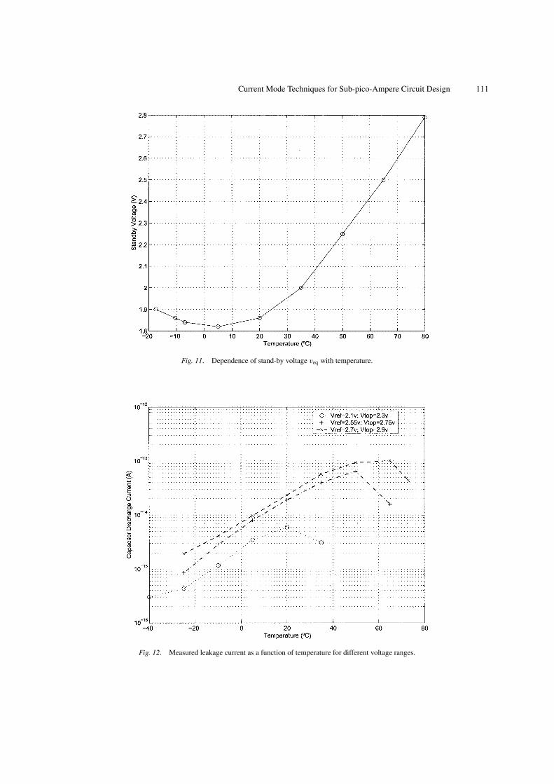
to two NMOS transistor diffusions (M3 and M2) and aPMOS transistor diffusion (M1). Consequently, therewill be positive and negative leakage currents, and thenet sum will either charge or discharge the capacitor.When all leakage currents balance out, the capacitorvoltage will remain constant at voltage veq. This volt-age can be measured experimentally by simply settingvoltage VREF in Fig. 4 sufficiently low (for example,VREF = 0V ). Figure 11 shows the dependence of thisvoltage with respect to temperature.
Obviously, in order to have a net capacitor dischargeleakage current, the saw-tooth oscillator must be op-erated with a capacitor voltage vc above veq. This iseasily achieved by controlling properly the maximumand minimum voltages of vc through VTOP and VREF,respectively. Under these circumstances, the saw-toothoscillator will operate properly, and we will be able tomeasure the discharging slopes, and consequently the
net discharging leakage current. Figure 12 shows, asa function of temperature, the net discharge currentsobtained experimentally for different voltage ranges(set through VREF and VTOP). As discussed previously,leakage currents behave more as a leakage resistance(at least, for voltages close to veq). This fact makes themeasured leakage currents in Fig. 12 to depend on thevoltage range.
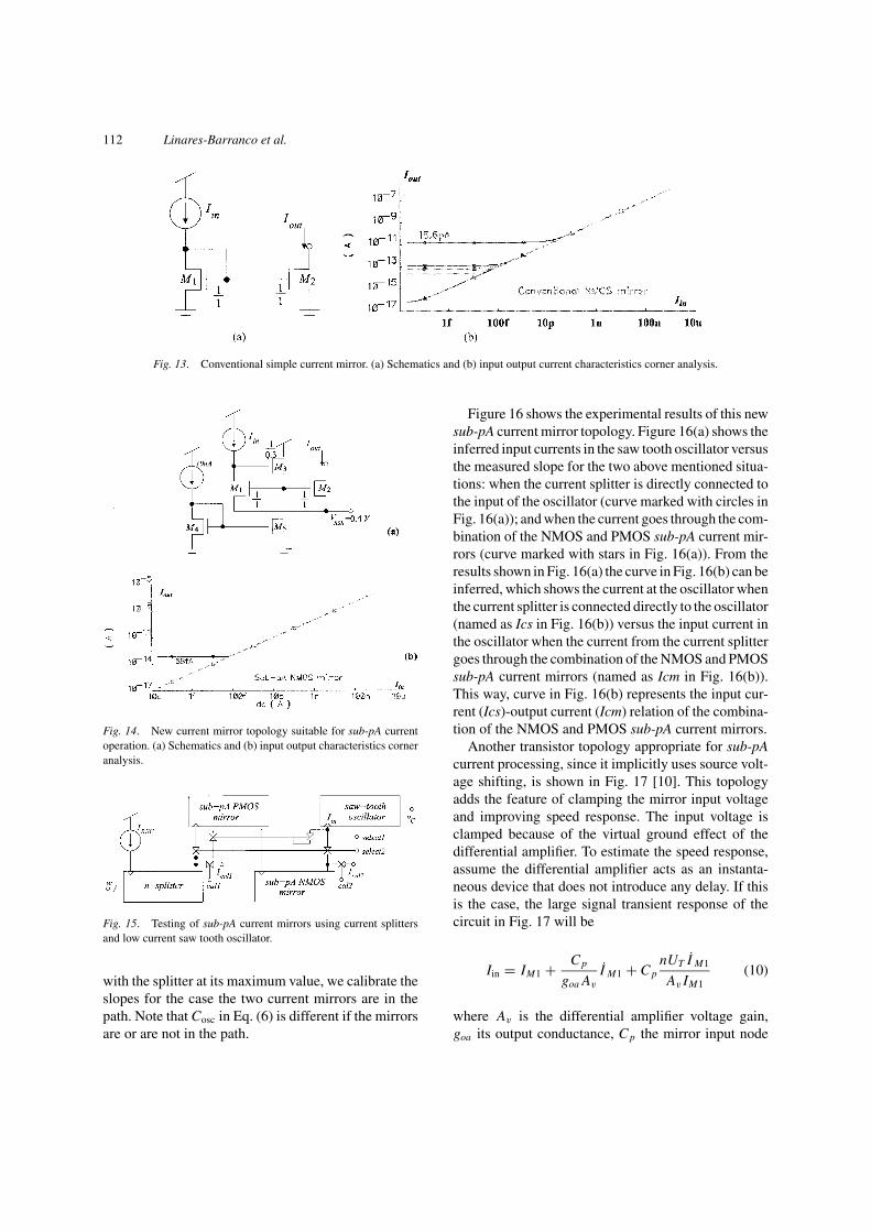
5. Sub-pA Current Mirrors
A fundamental building block for any current mode sig-nal processing circuit is the current mirror. Figure 13(a)shows the schematic of a conventional simple NMOScurrent mirror. Simulating its input output character-istics by sweeping Iin from 10−17 A to 1 µA whileperforming corner analysis reveals the results shownin Fig. 13(b) (drain voltage of output transistor M2 wasconnected to VDD/2). The worst corner minimum op-erating current for this mirror is 15.6 pA, well abovethe worst case reverse biased diffusion diode currents(about 70 fA in Fig. 2(b)). This is because transistorscannot be turned completely OFF. Shifting the sourcevoltages for this mirror does not solve the problem be-cause the gate voltage cannot go below the source volt-age for this topology. Using the topology in Fig. 14(a)allows the gate voltage to adapt below the shifted sourcevoltages. Transistors M3 − M5 implement a voltageshifter that makes the gate voltage of M1 to be onethreshold voltage below its drain. Performing corneranalysis simulations on this topology provides the re-sults shown in Fig. 14(b). The high temperature cor-ners saturate at the diffusion diodes leakage currents(69 fA), while the others remain fully operative downto 10 aA (10−17 A).
In order to test experimentally this current mirrortopology, a PMOS and an NMOS version was usedin combination with the current splitter and the sawtooth oscillator, as shown in Fig. 15. By setting signal‘select1’ high (and all others low) the current splitteroutput is connected directly to the saw tooth oscillator.Setting ‘select2’ high (and all others low) makes thiscurrent go through the two sub-pA NMOS and PMOScurrent mirrors. By setting signal ‘cal1’ high (and allothers low), while setting the splitter to its maximumvalue, we can measure externally the maximum currentprovided by the splitter. This allows us to calibrate theslopes of the oscillator when it is connected directly tothe splitter. By setting ‘cal2’ high (and all others low),
Current Mode Techniques for Sub-pico-Ampere Circuit Design 111
Fig. 11. Dependence of stand-by voltage veq with temperature.
Fig. 12. Measured leakage current as a function of temperature for different voltage ranges.
112 Linares-Barranco et al.
Fig. 13. Conventional simple current mirror. (a) Schematics and (b) input output current characteristics corner analysis.
Fig. 14. New current mirror topology suitable for sub-pA currentoperation. (a) Schematics and (b) input output characteristics corneranalysis.
Fig. 15. Testing of sub-pA current mirrors using current splittersand low current saw tooth oscillator.
with the splitter at its maximum value, we calibrate theslopes for the case the two current mirrors are in thepath. Note that Cosc in Eq. (6) is different if the mirrorsare or are not in the path.
Figure 16 shows the experimental results of this newsub-pA current mirror topology. Figure 16(a) shows theinferred input currents in the saw tooth oscillator versusthe measured slope for the two above mentioned situa-tions: when the current splitter is directly connected tothe input of the oscillator (curve marked with circles inFig. 16(a)); and when the current goes through the com-bination of the NMOS and PMOS sub-pA current mir-rors (curve marked with stars in Fig. 16(a)). From theresults shown in Fig. 16(a) the curve in Fig. 16(b) can beinferred, which shows the current at the oscillator whenthe current splitter is connected directly to the oscillator(named as Ics in Fig. 16(b)) versus the input current inthe oscillator when the current from the current splittergoes through the combination of the NMOS and PMOSsub-pA current mirrors (named as Icm in Fig. 16(b)).This way, curve in Fig. 16(b) represents the input cur-rent (Ics)-output current (Icm) relation of the combina-tion of the NMOS and PMOS sub-pA current mirrors.
Another transistor topology appropriate for sub-pAcurrent processing, since it implicitly uses source volt-age shifting, is shown in Fig. 17 [10]. This topologyadds the feature of clamping the mirror input voltageand improving speed response. The input voltage isclamped because of the virtual ground effect of thedifferential amplifier. To estimate the speed response,assume the differential amplifier acts as an instanta-neous device that does not introduce any delay. If thisis the case, the large signal transient response of thecircuit in Fig. 17 will be
Iin = IM1 + C p
goa Av
I M1 + C pnUT I M1
Av IM1(10)
where Av is the differential amplifier voltage gain,goa its output conductance, C p the mirror input node

Current Mode Techniques for Sub-pico-Ampere Circuit Design 113
Fig. 16. Experimental results of the sub-pA new current mirror topology. (a) Input current inferred in the saw tooth oscillator vs. measuredslopes when the current splitter is connected to the oscillator input and when the current goes through the NMOS and PMOS sub-pA currentmirrors. (b) Inferred input-output current behavior of the compound NMOS and PMOS sub-pA current mirrors.
Fig. 17. A source-driven active-input current mirror with implicitsource voltage shifting.
capacitance and IM1 the current through input transis-tor M1. If Iin changes in a step fashion from r Ic to Ic,the solution for Eq. (10) can be written as
IM1(t)
[Ic − IM1(t)]1+ε= r Ic
[Ic − r Ic]1+εet/τ1 (11)
where
τ1 = C pnUT
Av Ic, ε = Ic
goanUT(12)
If we define td1 as the delay time it takes for IM1(t) toreach RIc, then
td1 = τ1 ln
[R
r
(1 − r
1 − R
)1+ε](13)
Note that if Av is sufficiently large τ1 can be madevery small, even for low values of Ic. For example, ifC p = 0.1 pF, Av = 104 and Ic = 1 fA the resultingtime constant would be 356 µs, which is a very shorttime interval for a circuit operating at only 1 fA currentand handling a 0.1 pF capacitance.
6. Log-Domain Low-Pass Filter with Sub-HzCut-off Frequency
A very interesting application of sub-pA current modesignal processing is the capability of implementing ex-tremely long time constant circuits without relying onlarge capacitances. To illustrate this, a conventionalfirst-order log-domain CMOS filter was fabricated andtested. The schematic of the selected first order sec-tion is shown in Fig. 18 [11]. M5 and M6 are cascodetransistors for keeping the drain voltages of M1 andM4 equal. The low-pass filtering function is realizedby transistors M1 − M4 and capacitor CLPF. Assumingall transistors in their weak inversion saturation region,the equations describing the circuit operation are
Iin Ib1 = I3 Io
I3 = Ib2 + CLPFvC (14)
vC = nφtI o
Io

114 Linares-Barranco et al.
Fig. 18. Schematic of first order log-domain low-pass filter sectionfor sub-pA operation.
Assuming Ib1 = Ib2 = Ib Eq. (14) result in the follow-ing time domain differential equation
Iin = Io + τLPF Io(15)
τLPF = nφtCLPF
Ib
which describes a first order low-pass filter with 3 dBcut-off frequency ωLPF = 1/τLPF. For a 1 Hz cut-offfrequency with CLPF = 0.1 pF, n = 1.37, and φt =26 mV, the bias current should be Ib = 2πnφt CLPF
fLPF = 22.4 fA.The log-domain low-pass filter of Fig. 18 with
CLPF = 0.1 pF was fabricated in a 0.35 µm CMOSprocess together with an NMOS current splitter, a saw-tooth oscillator and a set of sub-pA current mirrors,as shown in Fig. 19. The area of the log-domain filteris 12 × 24.35 µm. It’s layout is depicted in Fig. 20.
Fig. 19. Fabricated circuitry for test of sub-pA log-domain low-pass filter.
Fig. 20. Layout of the log-domain first-order low-pass filter cell inFig. 18, with an area of 12 × 24.35 µm2.
Current IREF for the current splitter was supplied off-chip, as well as Ibe1, Ibe2 and the two 1 M� resis-tors. Ibe1, Ibe2, and VREF were adjusted to make theDC values va = vd and the low-pass transfer functionwas measured from vin to vo. The set-up in Fig. 19 al-lows us to control the value of Ib1 = Ib2 = Ib of thelow pass filter, while inferring that value by means ofthe saw-tooth oscillator. Figure 21 shows the measuredlow-pass filter frequency response for several values ofIb. Here IREF was set to 1 nA and the digital controlword w changed from 1 to 5. The values of the 3 dBcut-off frequency were respectively 0.5 Hz, 0.7 Hz,1.0 Hz, 3.5 Hz, 25 Hz and 50 Hz, while Ib was inferredto be 3.51 fA, 6.25 fA, 9.53 fA, 77.8 fA, and 1.24 pA(using the saw-tooth oscillator method of Section 5).When keeping w = 3 constant and changing IREF from55 nA down to 70 pA the set of values f3dB vs. Ib ofFig. 22 were measured. Both Figs. 21 and 22 were notmeasured using a spectrum/network analyzer, becausethe frequencies were too low. Instead, input and outputsinusoids were directly observed on an oscilloscopeand the output waveform amplitude was manuallymeasured as a function of input frequency.

Current Mode Techniques for Sub-pico-Ampere Circuit Design 115
Fig. 21. Measured frequency response of the log-domain low-pass filter for different Ib values.
Fig. 22. Measured 3 dB cut-off frequency of low-pass filter when setting control word w = 3 and sweeping IREF from 55 nA down to 70 pA.
7. Noise Estimation
It is possible to estimate the noise produced by the sub-pA MOS transistors by simply observing the saw-toothoscillator waveforms. Measuring its frequency jitter is
not a good way because it is produced not only by theinput current noise but also by the comparator inputequivalent noise. However, if we look at the saw-toothoscillator wave only during the time intervals capacitorCosc is being discharged, the voltage noise observed at

116 Linares-Barranco et al.
the capacitor is produced by the input current noiseand the analog buffer noise (see Fig. 5). Designing thisbuffer with sufficiently low noise, the noise observedat its output will be produced by the very low currentsdischarging capacitor Cosc. Naturally, the voltage noiseobserved at the output will be an integrated versionof the input current noise. Consequently, if the inputcurrent noise is white thermal noise, we should observea 1/ f 2 (−20 dB/dec) output voltage noise.
To measure the noise we proceeded as follows.The oscillator waveforms were recorded using a 16-bit ADC for several values of the input current. Thedischarging slopes were isolated and fitted to straightlines. These lines were subtracted from the dischargingslopes resulting in zero mean noise signals. These sig-nals were analyzed using Welch’s method for spectralestimation [12]. The results are shown in Fig. 23 for ca-pacitor discharge currents equal to 7 fA, 40 fA, 600 fA,and 7 pA. Naturally, the noise spectral density couldonly be measured to frequencies as low as the saw-toothfrequency itself. Even more, for frequencies close to theoscillation frequency, spectral content estimation canbe mistaken by distortion in the discharging slope. Ascan be seen in Fig. 23 all four noise measurements showthe expected −20 dB per decade slope. Consequently,only white noise is being produced by the input currentsfor the observed frequency ranges. The thermal (white)noise power spectral density expected to be producedby weak inversion MOS transistors is [13]
σ 2I = 2q I (16)
Fig. 23. Measured spectral noise density at discharging oscillatorcapacitor.
where q is the electron charge. Since this current noiseis integrated on capacitor Cosc during the dischargingramps, the voltage noise present at its terminal will be
σV = σI
2π f Cosc(17)
This theoretical noise is also shown in Fig. 23, for eachdischarging current, with straight lines. As can be seen,the measured noise resembles reasonably close the the-oretically predicted noise.
Flicker noise (1/ f ) in subthreshold can usually beneglected with respect to thermal noise. It would, inprinciple, become noticeable for very low frequencies,but the 1/ f dependence will not hold for arbitrarily lowfrequencies [14].
Using Eqs. (15) and (16) one can predict the signal tonoise ratio (SNR) for the Low-Pass filter of the previousSection. Thus,
SNR = I
σI√
� f=
√π I
qωLPF=
√nφt CLPF
q(18)
which shows that for this filter the signal to noiseratio is current independent and depends only thesize of capacitor CLPF. For the fabricated prototype,it was CLPF = 0.1 pF and n = 1.37, which yieldsSNR ≈ 40 dB, independent of current level (as longas the transistors are biased in weak inversion and onecan neglect flicker noise). Note that the fabricated ca-pacitor is fairly small, which means that SNR can beeasily improved by increasing CLPF.
8. Conclusions
We have shown that it is possible to design and ex-ploit reliably sub-pico-ampere current mode circuits.The key is to use “source-voltage shifting.” Currents inthe range of pA and well below can be reliably gener-ated on-chip by means of inversion level based specific-current extractors and logarithmic current splitters. Tomonitor sub-pA currents, a simple current driven saw-tooth oscillator can be included on-chip. An appropri-ate sub-pA current mirror topology has been introducedas well for proper current replication at such low val-ues. As an application, a very simple low-pass filterhas been designed, fabricated and tested. It is basedon log-domain circuit techniques. It uses 6 small sizetransistors, a 100 fF capacitor, and provides a 3 dB cut-off frequency of 0.5 Hz when biased with 3.51 fA. Fi-nally, it is shown how noise measurements can be easily
Current Mode Techniques for Sub-pico-Ampere Circuit Design 117
performed on transistors operating down to fempto-amps, and how such measurements resemble closeenough the corresponding theoretical predictions. Be-sides noise, mismatch considerations are also impor-tant for weak inversion operation. However, mismatchtends to stay current independent within weak inversionand it is expected that for sub-pico-ampere operationmismatch can be predicted with the same weak inver-sion models for higher currents [1, 9, 15].
Acknowledgments
This work was in part supported by spanish MCyTprojects TIC-1999-0446-C02-02, FIT-070000-2001-0859, TIC-2000-0406-P4-05 and EU project IST-2001-34124.
Note
1. In the simulations the current resolution was set to be 10−18 A.
References
1. E. Vittoz, “Micropower techniques,” in Design of VLSI Circuitsfor Telecommunication and Signal Processing, J. Franca and Y.Tsividis (Eds.), Prentice Hall: Englewood Cliffs, 1994.
2. A.G. Andreou, “Exploiting device physics in circuit de-sign for efficient computational functions in analog VLSI,”in Low-Voltage/Low-Power Integrated Circuits and Systems,E. Sanchez-Sinencio and A.G. Andreou (Eds.), IEEE Press:New York, 1999, pp. 85–132.
3. T. Delbruck and C.A. Mead, “Analog VLSI phototransduction,”CNS Memo No. 30, California Institute of Technology, April 2,1996.
4. E. Culurciello, R. Etienne-Cummings, and K. Boahen, “Highdynamic range, arbittered address event representation digitalimager,” in Proceedings of the 2001 IEEE International Sympo-sium of Circuits and Systems (ISCAS’01), 2001, vol. III, pp. 505–508.
5. C.C. Enz, F. Krummernacher, and E.A. Vittoz, “An analyticalMOS transistor model valid in all regions of operation and dedi-cated to low-voltage and low-current applications,” special issueof the Analog Integrated Circuits and Signal Processing Journalon Low-Voltage and Low-Power Design, vol. 8, pp. 83–114, July1995.
6. C. Galup-Montoro, M.C. Schneider, and A.I.A. Cunha, “Acurrent-based MOSFET model for integrated circuit design,”Chapter 2 in Low-Voltage/Low-Power Integrated Circuits andSystems, E. Sanchez-Sinencio and A.G. Andreou (Eds.), IEEEPress: Aug. 1998.
7. P. Heim, S. Schultz, and M.A. Jabri, “Technology-independentbiasing technique for CMOS analogue micropower implemen-tations of neural networks,” in Proceedings of the 4-th Interna-tional Worshoop on Cellular Neural Networks and their Appli-cations (CNNA-95), 1995.
8. K. Bult and J.G.M. Geelen, “An inherently linear and compactMOST-only current division technique.” IEEE Journal of SolidState Circuits, vol. SC-27, pp. 1730–1735, Dec. 1992.
9. C.C. Enz and E.A. Vittoz, “CMOS low-power analog circuitdesign,” in Proceedings of the IEEE International Symposiumof Circuits and Systems (ISCAS’96), Chapter 1.2 of Tutorials,1996, pp. 79–132.
10. T. Serrano-Gotarredona, B. Linares-Barranco, and A.G.Andreou, “Very wide range tunable CMOS/bipolar current mir-rors with voltage clamped input,” IEEE Transactions on Circuitsand Systems (Part I): Fundamental Theory and Applications,Nov. 1999, pp. 1398–1407.
11. J. Mulder, W.A. Serdijn, A.C. Van der Woerd, and A.H.M.van Roermund, Dynamic Translinear and Log-Domain Circuits:Analysis and Synthesis. Kluwer Academic Publishers: Boston,1998.
12. P.D. Welch, “The use of fast fourier transform for the estimationof power spectra: A method based on time averaging over shortmodified periodograms.” IEEE Transactions on Audio Electroa-coustics, vol. AU-15, pp. 70–73, June 1967.
13. J. Fellrath, “Shot noise behavior of subthreshold MOS tran-sistors.” Revue de Physique Apppliquee, vol. 13, pp. 719–723,Dec. 1978.
14. M.S. Keshner, “1/ f noise,” in Proceedings of the IEEE, vol. 70,no. 3, pp. 212–218, 1982.
15. B. Linares-Barranco and T. Serrano-Gotarredona, “On the de-sign and characterization of femtoampere current-mode cir-cuits.” IEEE Journal of Solid-State Circuits, vol. 38, pp. 1353–1363, 2003.
Bernabe Linares-Barranco received the B.S. de-gree in electronic physics in June 1986 and the M.S.degree in microelectronics in September 1987, bothfrom the University if Seville, Sevilla, Spain. He re-ceived a first Ph.D. degree in high-frequency OTA-Coscillator design in June 1990 from the University ifSeville, Spain, and a second Ph.D. degree in analogneural network design in December 1991 from TexasA&M University, College-Station, USA.
Since September 1991, he has been a Tenured Sci-entist at the “Instituto de Microelectronica de Sevilla”(IMSE-CNM-CSIC), Sevilla, Spain. From September1996 to August 1997, he was on sabbatical stay at theDepartment of Electrical and Computer Engineering

118 Linares-Barranco et al.
of the Johns Hopkins University, Baltimore, USA, asa Postdoctoral fellow. During Spring 2002 he was Vis-iting Associate Professor at the Electrical Engineer-ing Department of Texas A&M University, College-Station, USA.
He has been involved with circuit design for telecom-munication circuits, VLSI emulators of biological neu-rons, VLSI neural based pattern recognition systems,hearing aids, precision circuit design for instrumen-tation equipment, bio-inspired VLSI vision process-ing systems, transistor parameters mismatch character-ization, Address-Event-Representation VLSI, and RFcircuit design.
Dr. Linares-Barranco was corecipient of the 1997IEEE Transactions on VLSI Systems Best Paper Awardfor the paper “A Real-Time Clustering Microchip Neu-ral Engine,” and of the 2000 IEEE CAS DarlingtonAward for the paper “A General Translinear Principlefor subthreshold MOS Transistors.” He organized the1994 Nips Post-Conference Workshop “Neural Hard-ware Engineering.” From July 1997 until July 1999 hewas Associate Editor of the IEEE Transactions on Cir-cuits and Systems Part II, and since January 1998 he isalso Associate Editor for IEEE Transactions on NeuralNetworks. He is Chief Guest Editor of the IEEE Trans-actions on Neural Networks Special Issue on NeuralHardware Implementations. He is co-author of the book“Adaptive Resonance Theory Microchips.”
Teresa Serrano-Gotarredona received the B.S.degree in electronic physics in June 1992 fromthe University of Seville, Sevilla, Spain. She receivedthe Ph.D. degree in VLSI neural categorizers from theUniversity of Seville in December 1996, after complet-ing all her research at the Analog Design Departmentof the National Microelectronics Center (CNM),Sevilla, Spain. From September 1996 until August1997, she obtained as M.S. degree in the Departmentof Electrical and Computer Engineering of the JohnsHopkins University, Baltimore, MD, where she was
sponsored by a Fullbright Fellowship. She was on asabbatical stay at the Electrical Engineering Dept. ofTexas A&M university during Spring 2002. She wasAssistant professor at the university of Seville from1998 until 2000. Since June 2000 she holds a TenuredScientist position at the “Instituto de Microelectronicade Sevilla,” Sevilla, Spain.
Her research interests include analog circuit designof linear and nonlinear circuits, VLSI neural basedpattern recognition systems, VLSI implementations ofneural computing and sensory systems, transistor pa-rameters mismatch characterization, Address-Event-Representation VLSI, and RF circuit design.
Dr. Serrano-Gotarredona was corecipient of the 1997IEEE Transactions on VLSI Systems Best Paper Awardfor the paper “A Real-Time Clustering Microchip Neu-ral Engine” and of the IEEE CAS Darlington Awardfor the paper “A General Translinear Principle for Sub-threshold MOS Transistors.” She is co-author of thebook “Adaptive Resonance Theory Microchips.”
Rafael Serrano-Gotarredona received the B.S. de-gree in Telecommunications Engineering in 2002 fromthe University of Seville, Sevilla, Spain. He is currentlyworking towards his PhD degree at the “Instituto deMicroelectronica de Sevilla” (IMSE-CNM-CSIC).
His research interests include analog and mixed-signal VLSI circuit design applied to vision processingsystems.
Clara Serrano-Gotarredona received the B.S. de-gree in Telecommunications Engineering in 2001 from

Current Mode Techniques for Sub-pico-Ampere Circuit Design 119
the University of Seville, Sevilla, Spain. She is cur-rently working towards her PhD degree at the “Institutode Microelectronica de Sevilla” (IMSE-CNM-CSIC).
Her research interests include mixed-signal and dig-ital VLSI circuit design applied to vision processingsystems.


![[BiochemB] Signal Transduction - Dr. Viliran (Bernabe and Dela Rosa).pdf](https://static.fdocuments.in/doc/165x107/563dba4f550346aa9aa48048/biochemb-signal-transduction-dr-viliran-bernabe-and-dela-rosapdf.jpg)