CSIR - isssonline.inisssonline.in/wp-content/uploads/2016/11/sukshmaVol2No3small.pdf · project...
8
The Centres of Excellence in Nanoelectronics at lIT-Bombay and IISc-Bangalore, funded by the Ministryof Communication and Information Technology (MCIT), are takingshape. Both will be national laboratories 3 equipped with the capability to fabricate devices with fine geometries, which will be made availableto 3 researchers from aroundthe country. To make known the planned capabilities of the two facilities to the potential user community, both from theacademia and the industry, and to seek the input of the intended 4 users, a two-day workshop entitled, Indian Nanoelectronics Users' Program (INUP) Awareness Workshop, 6 was held onthe IISc campus, Bangalore, on April 9-10,2007. Researchers active in thefield of nanotechnology, .6 nanomaterials, electronic device physics and technology, as well as those intending to enter these fields were invited to participate inthe Workshop. It isan encouraging sign thatmore than 60 participants from around 7 the country attended the Workshop.Thesignificance of thefacilities being established was underlined by 7 the fact that theDirectors of IIT- Band IISc, as well as Dr. Phadke of the MCIT, werepresentat the opening session. The Workshop was inaugurated by Prof. P. Balaram, Director, TISc, who pointed out that the USc was committingsignificant resources to the programthrough thefunding of a new building to house the fabrication facility. Prof. A. Mishra, Director, TIT-B, noted that a most significant input intosuch programs was the recruitment and retention of talented researchers, and that it would be very advisableand necessary to make academic positions more remunerative. Healso added that a new building will beconstructed at IIT-B to house the program, in addition to thespace being provided in an existingstructure. Dr. PhadkeofMCIT outlined the research programsand initiatives that the Ministry intended to support, and pointedoutthat there would be no dearth of support for well-considered and technically significant proposals. Theopening session was followedby detailedpresentations on the facilities beingcreated at JIScand lIT-B. Prof. S. Mohan of JISc described the program evolving at IlSc with some 45 faculty members from various departments to be involved in the Centre, which will be housed inabrand-new building measuring 90,000 sq.ft, of which 10,000 sq.ft. will be thecleanroom fab. Prof. V. RamgopalRao described the facility being built at IIT-B, highlighting the participation of researchers from a number of disciplines. He detailed the facilities already available at lIT-B, and noted that JIT-B would be setting up a clustertool being donatedbyAppliedMaterials, Incof theUSA. Both Prof. Mohan and Prof. Rao noted that, in keeping with the proposalmade to the MCIT, many of the facilities will be common,and wherever possible, fabtools would be procured from thesame vendor. Thisprovides redundancylbackup, apart from providinga better bargaining position with vendors. The teams at lIT-B and IISc are in constant communication and consultation with each other, and will continue tobeso, underlined a MoU being signed by JIT-B and JISc in this regard. (See a related report onp. 7)." ,'::;' .' Dr. SA Shivashankar is an Professor in the Materials Research Centre in IISc. He canbe reached at shiva@mrc.iisc.ernetin. Council of Scientific and IndustJialResearch (CSIR) undertook a networked R&D Project (multi-laboratory coordinated R&D project) on MEMS duringthe 10 th Five Year Plan of thegovernment of India. The project involved nine CSIR laboratories (see box below), which pooled their expertise in multiple disciplines to achieve common objectives of developing MEMS-based microsensor structures, development of sensing materials including novelnanomaterials, development of prototype sensors for different applications, and their evaluation and characterization. TheMEMS and microsensor platfornls developed under the programme include: (a) ISFET: ion-sensitive field-effect transistor,(b) microhotplate device, (c) Micro-channel electrophoretic device, (d) micro- cantilever-based device, and (e) polymer gas sensor device.Utilizing theseplatforms and specialized materialsand techniques developed under the programme, following prototype microsensors have beendeveloped: pH sensor,glucose sensor, triglyceride sensor, potassium and calcium ion sensors (allusing ISFET platform), smoke sensor and carbonmonoxide sensor (using hybridmicrocircuit hotplate), ammonia, hydrogen sulphide and carbon monoxide sensors(using polymer-based gas microsensor), cholesterol biosensor using SPR, dopamine sensor (using micro-channel electrophoretic device includingelectro-chemical sensing electrodes), methane and LPG sensors (see Vol. 2, No.2, p. 7) using ceramic wire-wound heaters. The programme had a duration of five yearsendingonMarch 31, 2007, and a total outlay of Rs.31.71 crores.Under the programme, the MEMS laboratory at CEERI has also been equipped with 6" wafer processing facilities including oxidation and diffusion furnaces, anodic bonding facility, deepreactive ion etching facility, double spindle dicing machine, chem-mech lappingand polishing machine, acoustic imager,sUlface profiler and gas sensor characterization facilities. These facilities complement theearlier existing facilities of LPCYD, metallization and photolithography to makea complete R&D MEMS laboratory for 6" wafer size .••• Nine Networked CSIR Laboratories for the Program I. Ccntral Electronics Engineering Rcsearch Institutc (CEERI). Pilani. 2. National Physical Laboratory (NPL), Delhi. 3. Indian Institute of Chemical Technology (IICT). Hyderabad. of. National Chemical Laboratory (NCL). Pune. 5. Central Electro-chemical Research Institute (CECRI). Karaikudi. 6. Rcgional Research Laboratory (RRL). Bhopal. 7. Centrc for Cellular and Molecular Biology (CCMB). Hyderabad. 8. Ccntral Glass and Ceramics Research Institute (CGCRI). Kolkata. 9. Central Mechanical Engincering Research Institute (CMERI), Durgapur. Dr. Chandra Shekhar is the Director of CEERI, the CSIR lab which coordinated the network project on MEMS. He can be reached at [email protected].
Transcript of CSIR - isssonline.inisssonline.in/wp-content/uploads/2016/11/sukshmaVol2No3small.pdf · project...

The Centres of Excellence in Nanoelectronics at lIT-Bombay and IISc-Bangalore, funded by the Ministry ofCommunication and Information Technology (MCIT), are taking shape. Both will be national laboratories
3 equipped with the capability to fabricate devices with fine geometries, which will be made available to3 researchers from around the country. To make known the planned capabilities of the two facilities to the
potential user community, both from the academia and the industry, and to seek the input of the intended4 users, a two-day workshop entitled, Indian Nanoelectronics Users' Program (INUP) Awareness Workshop,6 was held on the IISc campus, Bangalore, on April 9-10,2007. Researchers active in the field of nanotechnology,
.6 nanomaterials, electronic device physics and technology, as well as those intending to enter these fields wereinvited to participate in the Workshop. It is an encouraging sign that more than 60 participants from around
7 the country attended the Workshop. The significance of the facilities being established was underlined by7 the fact that the Directors of IIT-Band IISc, as well as Dr. Phadke of the MCIT, were present at the opening
session. The Workshop was inaugurated by Prof. P. Balaram, Director, TISc, who pointed out that the USc wascommitting significant resources to the program through the funding of a new building to house the fabrication facility. Prof. A. Mishra, Director,TIT-B,noted that a most significant input into such programs was the recruitment and retention of talented researchers, and that it would be veryadvisable and necessary to make academic positions more remunerative. He also added that a new building will be constructed at IIT-B to housethe program, in addition to the space being provided in an existing structure. Dr. Phadke of MCIT outlined the research programs and initiatives thatthe Ministry intended to support, and pointed out that there would be no dearth of support for well-considered and technically significantproposals.The opening session was followed by detai led presentations on the facilities being created at JISc and lIT-B. Prof. S. Mohan of JISc described theprogram evolving at IlSc with some 45 faculty members from various departments to be involved in the Centre, which will be housed in a brand-newbuilding measuring 90,000 sq.ft, of which 10,000 sq.ft. will be the clean room fab. Prof. V. Ramgopal Raodescribed the facility being built at IIT-B, highlighting the participation of researchers from a number ofdisciplines. He detailed the facilities already available at lIT-B, and noted that JIT-B would be setting upa cluster tool being donated by Applied Materials, Inc of the USA. Both Prof. Mohan and Prof. Rao notedthat, in keeping with the proposal made to the MCIT, many of the facilities will be common, and whereverpossible, fab tools would be procured from the same vendor. This provides redundancylbackup, apartfrom providing a better bargaining position with vendors. The teams at lIT-B and IISc are in constantcommunication and consultation with each other, and will continue to be so, underlined a MoU beingsigned by JIT-B and JISc in this regard. (See a related report on p. 7)."
,'::;' .'
Dr. SA Shivashankar is anProfessor in the MaterialsResearch Centre in IISc. Hecan be reached [email protected].
Council of Scientific and IndustJial Research (CSIR) undertook a networked R&D Project (multi-laboratorycoordinated R&D project) on MEMS during the 10th Five Year Plan of the government of India. Theproject involved nine CSIR laboratories (see box below), which pooled their expertise in multipledisciplines to achieve common objectives of developing MEMS-based microsensor structures,development of sensing materials including novel nanomaterials, development of prototype sensorsfor different applications, and their evaluation and characterization.
The MEMS and microsensor platfornls developed under the programme include: (a) ISFET: ion-sensitivefield-effect transistor, (b) microhotplate device, (c) Micro-channel electrophoretic device, (d) micro-cantilever-based device, and (e) polymer gas sensor device. Utilizing these platforms and specialized materials and techniques developed underthe programme, following prototype microsensors have been developed: pH sensor, glucose sensor, triglyceride sensor, potassium and calciumion sensors (all using ISFET platform), smoke sensor and carbon monoxide sensor (using hybrid microcircuit hotplate), ammonia, hydrogensulphide and carbon monoxide sensors (using polymer-based gas microsensor), cholesterol biosensor using SPR, dopamine sensor (usingmicro-channel electrophoretic device including electro-chemical sensing electrodes), methane and LPG sensors (see Vol. 2, No.2, p. 7) using
ceramic wire-wound heaters.The programme had a duration of five years ending on March31, 2007, and a total outlay of Rs.31.71 crores. Under theprogramme, the MEMS laboratory at CEERI has also beenequipped with 6" wafer processing facilities including oxidationand diffusion furnaces, anodic bonding facility, deep reactiveion etching facility, double spindle dicing machine, chem-mechlapping and polishing machine, acoustic imager, sUlface profilerand gas sensor characterization facilities. These facilitiescomplement the earlier existing facilities of LPCYD, metallizationand photolithography to make a complete R&D MEMSlaboratory for 6" wafer size .•••
Nine Networked CSIR Laboratories for the ProgramI. Ccntral Electronics Engineering Rcsearch Institutc (CEERI). Pilani.2. National Physical Laboratory (NPL), Delhi.3. Indian Institute of Chemical Technology (IICT). Hyderabad.of. National Chemical Laboratory (NCL). Pune.5. Central Electro-chemical Research Institute (CECRI). Karaikudi.6. Rcgional Research Laboratory (RRL). Bhopal.7. Centrc for Cellular and Molecular Biology (CCMB). Hyderabad.8. Ccntral Glass and Ceramics Research Institute (CGCRI). Kolkata.9. Central Mechanical Engincering Research Institute (CMERI), Durgapur.
Dr. Chandra Shekhar is theDirector of CEERI, the CSIRlab which coordinated thenetwork project on MEMS. Hecan be reached [email protected].
I feel happy and proud to be taking charge as the President of the Institute of Smart StructuSystems. The out-going Executive Council, under the able leadership of Prof. S. Mohan, vi .guidance from Dr. V .K. Aatre, Founder President, and with the whole-hearted support and coopera , "",:::from the members, has done an excellent job of strengthening the society, expanding the scope ofi~~""'"activities to the educational sector (with full support from Dr. K. Balaveera Reddy, the erstwhile ViceChancellor ofVTU), and introducing new elements of communication with the community such as thisnewsletter "Sukshma" and the website, opening a dialogue with the user industry on MEMS, etc. Weneed to build on these initiatives and move forward with renewed vigor and commitment to meet theobjectives and goals of ISSS.
Thanks to major national initiatives such as NPSM (.I eeVol. I No. I, p. I) and DISMAS, and active andenthusiastic participation of the community in these initiatives, the country has made good progress inthis vital and strategically important area. The technology of smart materials, structures and systems,including micro-systems, has matured today to move from R&D in the laboratories to industry specificproducts such as micro-sensors (pressure, gas, acceleration, RF, vibration, rotational rate, etc.) and
• - • l' piezo and SMA actuators, and applications at a practical level such as Structural Health Monitoring,Vibration and noise control , Shape control, Mechanisms, etc. This opens up new and excitingpossibilities in design, particularly in aerospace and bio-medical sectors apart from innumerable
applications in automotive, chemical, food, and environment and other sectors. It is practical applications in these sectors that the next phaseof the national initiative from the Government, in final stages of consideration and approval, plans to target in the next five years. Thestrategic and social benefits of such technologies must be exploited to the fullest extent, and ISSS has a major and important role to play here.I am happy to be leading a young (yet tremendously experienced!) and enthusiastic team who are committed to the goals of the society andlove their work. Our tasks in the coming two years are clear cut;(i) Help in the efficient and effective implementation of national initiatives by active participation in their planning and implementation.(i i) Organi:ing the next international conference on Smart Materials, Structures and Systems (IC-SMSS 2008) in 2008. I am glad that
the Management of Bharat Electronics Ltd., Bangalore, which is a leading institution in the area of microsystems development, hascome forlVard to lead this activity with support from USc and NAL in their Centenary and Golden Jubilee years respectively.
(iii) Expand the base of the society by strengthening the existing chapters at Delhi, Bangalore and Hyderabad and opening morechapters where a nucleus of activity exists; membership drive to be taken up with increased emphasis.
(i v) Human Resource Development: build on the already initiated activity with VTU on faculty training and introducing new curriculumon smart and micro systems and help spread the concept to other universities and institutions.
(v) Promote interactions with Industry through Industry Federations to spread awareness and increased application of 'Smart'products and technology in their products.
(vi) Information Dissemination: Bring out publications such as Monograph on Active Vibration Control and other such publications,Conference proceedings, Continuous Website upgrading, support Newsletter, Organize national level events (workshops, seminars,etc.)
(vii) Bring in Nano technology activity into the Society '.I fold as a logical extension of micro-systems technology(viii) Support out-of-box-thinking and ideas; after all 'smart' is nothing but innovation! ~The Executive Council seeks your support and cooperation in our endeavors. Let us take ISSS to greater heights together. ~
I.SSS News S. Gopalakrishnan I
ISSS Annual General Bod) MeetIng (AGM) for the year 2007 \\:as held on April5'h, 2007 at AL. Bangalore. The meeting \\as preceded b)three techmcaltalks on some emerging areas in smart technolog) from three speaker'>, two from the National Institutes of Techno log) ( IT)at Trich) and Surethkal. and the third from the IISc. Dr. Umapathy from NIT-Trich), Dr. Hegde from NIT Surathkal. and Dr. D. Ro) :'1ahapatrafrom IISc made presentations. This was followed by the AGM, which was presided over b) the President of ISSS. Prof. S. Mohan. In hiswelcome aduress. Prof. Mohan. highlighted the achievements of the outgoing committee especiall). in the area of Human Resourceue\elopmenl. resurrection of the newsletter and in increasmg the membership. After the presentation of the secretary's and treasurer'sreports, AGM electeu the ne\\ team (.I eebelow under "ISSS Executive Council") to carryon the activities ofISSS for the next two years. Theelection was conducted by Prof. B. Datatguru. the past president of ISSS. Some new members were also inducted into the Executive Council.After taking over the mantle from Prof. Mohan. Dr. Upadhya placed on record his deep appreciation for the work done by the last committeeand cmphasi/ed the need to continue '>ome of the activitie'> initiated by the outgoing committee. He spelled out his priorities and vision forthe ne\\ committec especlall) in regard to increasing the membership. starting of many local chapters. initiating man) ne\\ monographs. and,1150 to make a fora) into nanotechnology."
__ E_d_i_t_o_r_ia_I_Ti_e_a_m__ II IS_S_S__ E_x_e_c_u_t_iv_e_C_o_u_n_c_il ~G.K. Ananthasuresh, IISc (Editor)S. Gopalakrishnan, IIScJ. Gurudutt, BigTecG.M. Kamath, NALK.J. Vinoy, IISc
Art Design: G. Bharathi
This newsletter is sent to allISSS members by postal mail.
President: A.R. Upadhya Vice-president: P.O. MangalgiriSecretaries: S. Gopalakrishnan and K. Vijayaraju Treasurer: G.M. Kamath
Members: s. Mohan, J. Gurudull, G.K. Ananthasuresh, and the presidents 01 Hyderabad and Deihl chapters
ISSS admission fee: Rs. 200Member:
Rs. 200 (annual); Rs. 2,000 (life)Student member:Rs. 75 (annual)
Corporate member:Rs. 10,000 (annual); Rs. 50,000 (life)
Payable to "ISSS, Bangalore".
and send the form with payment to~rum
Software International Limited (CSIL) is a publicly listed company that makes and sells scientific softwarepack es allover the world. With a very humble beginning in the early nineties in Bangalore as a tiny company
:',',', '111 ttibuting third party software products such as MATLAB, it now consists of more than 700 people, 15 shrink-wrapped products (including SYSTAT, SigmaPlot, and NISA), and 15 offices worldwide. Naturally, it has been recognizedas one of the fastest growing companies in Asia with award winning business process innovations. This, however, isonly part of the story. The company is fully committed to research driven innovations and products. In fact, it issurprising to see a company of such small size making commitments for long-term research. But, that is precisely whatthis company did by establishing the CranesSci MEMS Lab in March 2003, injoint collaboration with the Indian Institute of Science (lISc),Bangalore. CranesSci MEMS lab was conceived as the first such lab in the country in the area ofMEMS, funded largely by a private company.With this lab, CSIL embarked upon an ambitious but cautious plan to incubate and nurture micro and nano technologies with a product focus.The chief mandate of the CSIL team working in this area is intellectual property generation for MEMS products and technologies.
From its inception in 2003, the CSIL team's projects at CranesSci MEMS Lab are selected to build competencies required to complete a typicalproduct development process in the MEMS domain. CSIL already holds ajoint patent with lISc on a MEMS microphone design. The team isnow focused on developing system integration capabilities for MEMS products. In a related development, the lab has built a considerableknowledge base while working on MEMS based load cell for high weight applications. This work allowed the engineers to mesh multiple
knowledge and functional domain competencies to overcome numerousengineering challenges in the design and development of a MEMS load cellsystem. The figure on the left shows the complete integrated module on whichcharacterization has been carried out. In yet another related development, CSILhas created a wireless display system that can be interfaced with MEMS sensors(see p. 7 under Technology News).
The CSIL team of engineers enjoy an unprecedented freedom in terms of their pursuit of creative work and innovative ideas. Suchinitiatives from companies like CSIL have potential of nurturing a whole generation of a new breed of engineers.'"
:":,\:,::1:':'::',:
dustry Watch: Cranes Software IntI. Ltd.
I Leaders of ISSS
Dr. Sangineni Mohan, currently a Professor in the Department of Instrumentation, Indian Institute of Science (lISc),is also the Principal Investigator of a major programme, "Centre of Excellence for Nanoelectronics" at lISc, and theChairman of the Alumni Cell oflISc. He was the Chairman of the Department of Instrumentation in lISc during 1995-97, the Director of Central Scientific Instrument Organisation (CSIO), Chandigarh, during 1997-99, the Chief executiveof the Society for Innovation and Development (SID) in lISc during 2001-2006, the President of the InstrumentSociety oflndia during 1998-2006, and the President oflSSS during 2005-2007. In these and other capacities, he tookexemplary leadership role in initiating numerous new activities and fostering networking among the academia, industryand government R&D organizations.
As the Chief Executive of SID, he has been responsible for not only setting up interaction for JISc faculty withindustries in areas such as Information Technology, Biotechnology, Micro and Nano, and Automotive technologiesbut also networking with various R&D institutions and industries from within the country as well as from abroad. As the Director, CSIO he wasresponsible for networking CSIO with other R&D institutes, academic institutions, and industries, and executing challenging projects such asHead-up display for light combat Aircraft (LCA). He was also responsible for transferring technologies developed at CSIO to variousindustries. As the co-chairman of core group of automotive research (CAR), he is playing an active role in bringing academia, industry andresource persons from abroad together and preparing a status report for the future of transport industry in India. The successes of thisactivity has resulted in his interaction with the machine tool industry, which needs innovation for its survival. As the President of ISSS, hehelped expand the activity in the area of Microelectromechanical Systems (MEMS) in the country and foster international collaboration, andhelp start MEMS industry in India. As a member of Instrumentation committee formed by INSA, he has contributed to a report that gave avision for R&D in instrumentation activity in the country. His leadership has helped spread the instrumentation culture in the country.
Professor Mohan's accomplishments in research compete with his successes in leadership and networking. He has been working in the area ofthin-film technology for almost four decades. Novel methods of thin film deposition, modeling of thin film growth, process parameter- property-structure correlation, and fabrication of multi layer thin film devices are some of the highlights of his research. This work has enabled him to getinto the Round Robin of Optical Society of America on Ti02 coatings in 1985. He continued to be an active participant in the Laser DamageAnnual Symposia held at Boulder, Colorado, USA. During the period 1985-1992 he was closely interacting with Air Force Weapons Laboratory,Albuquerque. He has handled a number of challenging R&D projects on the development of thin film synthesis techniques and devices. Hismajor contribution to defence is the development of Head-Up Display System For Light Combat Aircraft (LCA) for which his group has beenawarded CSIR Technology award by the Honorable Prime Minister. He was a Visiting Professor at Forschung Centrum, Julich, Germany (1990),Pennsylvania State University (1994), RMIT, Melbourne (1998) and University of Arkansas (2005-06).
Professor Mohan has also contributed to technical education in the country. As a member ofthe vision committee ofVisweshwaraiah TechnologicalUniversity (VTU) he is helping VTU set up a centre of excellence in Bangalore in the Society model to bring the multinational companies toimpart training to faculty, students of all engineering colleges in the state and industries in Bangalore. During his tenure as the President of ISSS,a major effort to introduce an undergraduate course on Micro and Smart systems in VTU was taken by ISSS.
ISSS thanks Professor Mohan for his leadership and contributions in research and education .•••i,,::,I;'

Ni-Ti Shape Memory Alloys: Smart Metallic Materials
Shape Memory Alloys (SMAs) are materialsthat have two (or sometimes several)crystallographic phases for which reversibletransformations from one to the other occurthrough diffusionless transformations (theso-called "reversible martensitictransformations"). Two remarkable effectsare related with this phase change: the shapememory effect and the superelasticity. Theshape memory effect (SME) refers to theability of the material, initially deformed inits low-temperature phase (called"martensite"), to recover its original shapeupon heating to its high temperature phase(called austenite or "parent phase"). TheSME is a macroscopic effect of thermallyinduced crystallographic phase changes.The superelasticity occurs when themartensitic phase transformation is stressinduced at a constant temperature. Thetransformation is characterized by a plateauand a hysteresis upon unloading. Themagnitude of reversible 'pseudoelasticstrain' can be as high as 8% or even morefor single crystals. These phenomena areillustrated in Fig. I.
The physical performance of the NiTi alloymade it a landmark discovery in 1962, andthe range of commercially viableapplications that have been found for thisclass of materials is a proof of theimportance of the nickel-titanium (NiTi)shape memory alloys. But the discovery mayhave been a happy accident. Rumour has itthat William Buehler, who was working withhigh nickel-bearing alloys for gas turbinecomponents, left a small ingot of NiTi alloymade in a vacuum melt furnace on a desk indirect sunlight. When Buehler and hiscolleagues came back from lunch, theynoticed the ingot's shape had changed. Nowknown as Nitinol (derived from Ni-Ti NavalOrdinance Laboratories, a part of the USDepartment of Defence), the name hasbecome one of the commonly used titles forthe SMAs emanating from Buehler'slaboratory.
The nickel-titanium alloy has some of themost useful characteristics in terms of itsactive temperature range, cyclicperformance, recoverable strain andrelatively simple thellllaJ processing. NiTi andother alloys have two generic properties,namely, the thermally induced shaperecovery and super- or pseudo-elasticity.The latter means that an SMA in its elasticform can undergo a deformationapproximately ten times greater than that ofa spring-steel equivalent, and full elasticrecovery to the original geometry may beexpected. This may be possible throughseveral thousand cycles. The energydensity of the alloy can be used to good
(a)(b) T>A,
T<A,
t 1 Fig. 1. Schematics showing'"
'" '":!l '" (a) shape memory effect and.... V5
V5 (b) pseudo-elasticity.Unloading
effect to make high-force actuators. Amodern DC brush less electric motor has amass of 5-10 times that of a thermallyactivated NiTi alloy, to do the same work.
The success of NiTi SMAs in engineeringapplications is due to the uniquecombination of properties that they posses.Recoverable strains up to 8% and recoverystress up to 800 MPa are possible ifappropriate processing methodology isadopted. These compare to just 4% and 200MPa respectively in Cu-base alloys (TableI). The other decisive factors for the choiceof NiTi SMAs over other SMAs are superiormechanical properties, durability in terms ofstructural and functional fatigue, andcorrosion resistance. The ductility of thesealloys is remarkable among manyintermetallics, which are usually brittle.Ductility values more than 50% in martensitephase and 20% in austenite phase can easilybe obtained in NiTi SMAs. This makes theprocessing of these alloys from cast ingotsto semi-finished products to finishedproducts relatively easy compared to otherintermetallic alloys.
The first industrial application of NiTi SMAsin aeronautics was demonstrated with theCryofit connector for F-14 airplane hydrauliccircuits in late 1960s. Hydraulic couplino(Fig. 2) remains one of the earliest, yet, th:most successful engineering application andaccounts for the largest tonnage usage ofNiTi SMAs till date. The other applicationsinclude fasteners, electrical connectors ,actuators and sensors, release mechanisms,triggering devices, fuel injection, ventilationcontrol etc. Superelastic applications suchas foldable antennas for cellular phones,
Fig. 2. Shrink ring made of NiTi SMAfor hydraulic coupling
eyeglass frame are also quite popular in frecent times. ~
The concept of smart structures has thrownaltogether a new and exciting field for NiTiSMA applications. Extensivemultidisciplinary research is being pursuedworldwide in this regard. It has beendemonstrated that the shape recovery forcegenerated by NiTi SMA actuators, owingto the capability of adapting their reactionto the given environment, can be effectivelyutilized for buckling and shape control offlexible structures. Sincere efforts have beenmade during the past two decades tointegrate the functional properties of SMAsto obtain structural response more like abiological system. So far, success in thisregard has been very limited and efforts areon to make it a reality. Once this is achievedthe use of NiTi SMAs is bound to show a~unprecedented growth in the field ofengineering applications. The developmentof so-called adaptive, multifunctional, smartor intelligent structures with NiTi SMAs asthe smart element is likely to dominate thefuture structural technology.
Conventional actuating principles used atthe micro-scale do not scale downfavourably from a manufacturing as well asfrom an efficiency viewpoint. It requiresactuating principles that can be easilyintegrated and miniaturized and that cangenerate enough power input.Microactuators fabricated with NiTi takeadvantage of this material's large energydensity (-5-10 joules/cm3) and high strainrecovery (-8%). MicroelectromechanicalSystems (MEMS) devices designed withthese actuators can serve as biosensors,micro-fluidic pumps or optical switches.
Though the success story of NiTi SMAsbegan with engineering applications, thenonlinear stress-strain behaviour of thematerial was found to be very advantageousfor medical applications. Once thebiocompatibility of NiTi was proven andaccepted, NiTi SMAs opened up newopportunities for innovative devices andprocedures in medicine. The higher cost ofNiTi SMAs when compared to conventional

Shape Memory Alloys: Smart Metallic Materials
350*80**
CuZnAI FeMnSiCrNi
400* 1100130**
500-800 1600
-15 30
4 3
-200 300
Poor Good
Fair Low
200-700*70-140**
medical grade stainless steels such as the304 and 316 did not prevent successfulcommercialization of these productsbecause of the balance between the benefitto the patient, the host response, and thelifetime of the components.
There are a number of examples where NiTiSMAs have replaced the use of stainlesssteel and titanium alloy in biomedicalimplants. Also, minimally invasive surgeryhas been possible with the use of devicesmade of superelastic NiTi SMAs. Theseinclude guidewires for catheters, stentsand various filters, actuators for artificialheart and kidney pumps, orthodonticwires for dental braces, and implants.There is a growing market for NiTi SMAsin clinical instruments as well. Theseinclude biopsy forceps, tissue ablators,hingeless graspers, and retrieval basketsfor laparoscopy, to name a few. Theapplications ofNiTi SMAs in medicine areexpanding at a rapid rate and today, theyaccount for the maximum market share interms of money. A couple of applicationsare described next.
The property of thermally induced elasticrecovery can be used to change a smallvolume to a larger one. An example of adevice using this is a stent (Fig. 3), eitherin conjunction with a dilation balloon orsimply by self-expansion, can dilate orsupport a blocked conduit in the humanbody. Coronary artery disease, which is amajor cause of death around the world, iscaused by a plaque in-growth developingon and within an artery's inner wall. Thisreduces the cross-section of the artery andconsequently reduces blood flow to theheart muscle. A stent can be introduced ina "deformed" shape, in other words witha smaller diameter. This is achieved by
passing through the arteries with the stentcontained in a catheter. When deployed,the stent expands to the appropriatediameter with sufficient force to open thevessel lumen and reinstate blood flow.
The same technique can be employed inmany of the body's conduits, including theoesophageus, trachea, biliary system andurinary system. The technology of self-expansion or balloon-assisted expansion isused for many millions of these stents eachyear and the numbers are steadilyincreasing.
Another commercially important biomedicalapplication is the use of superelastic andthermal shape recovery alloys fororthodontic purpose. For many years,archwires made of stainless steel have beenin use as a corrective measure for misalignedteeth. Owing to the limited "stretch" andtensile properties of stainless steel wires,considerable forces are applied to teeth,which can cause a great deal of discomfort.When the teeth succumb to the correctiveforces applied, the stainless steel wire hasto be re-tensioned and requires frequentvisits to the orthodontist during the initialstages of treatment. Superelastic SMAwires are now used for these correctivemeasures. Owing to their elastic propertiesand extendibility, the level of discomfort canbe reduced significantly as the SMA appliesa continuous, gentle pressure over a longerperiod and hence, visits to the orthodontistare reduced to perhaps three or four peryear (Fig. 4).
The exciting field of smart materials isexpanding rapidly, with one of the mostinteresting areas being that of shapememory alloys. Surprisingly for materialswith so many applications, shape memory
I) K. Otsuka and C. M. Wayman,Shape memory materials,Cambridge University press,Cambridge, (1998).
2) T. W. Duerig, K.N. Melton, D.Stockel and C.M Wayman,Engineering aspects of shapememory alloys. Butterworth-Heinemann, New York, (1990).
3) J. Perkins, Shape memoryeffect in al/oys. Plenum Press,New York, (1975).
Fig. 4. Schematic illustration of theeffectiveness of NiTi SMA in comparisonwith stainless steel for orthodonticapplications
alloys have not been around for a long time.Tremendous progress has been made in thescience and technology of NiTi SMAs inrecent years. The avenues for research anddevelopment in NiTi SMAs are seeminglyendless and are increasing further with theadvent of new applications in bothengineering and biomedical fields .•
Dr. Subir K. Bhaumik is a scientist inthe Materials Science division of theNational Aerospace Laboratories(NAL). Bangalore. He can bereached at [email protected].
University Buzz: Micro "juice" flowing in
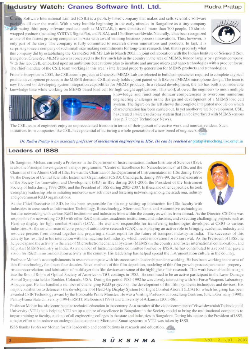
~ The Jadavpur University IC Centre (juiccentre for short; seewww.juiccentre.res.in) is a centre of excellence for Integrated Chip (Ie) design
and fabrication. It is located in Jadavpur, Kolkata. This centre was established in 1986 bythe department of electronics and telecommunication at the Jadavpur University. Today,it is one of the nation's thriving academic research centres working in the area of electronicsand microsystems devices. The centre has more than 10 faculty members who are workingon a variety of topics. The centre is equipped with e-beam and thermal depositions units,an RF supttering system, oxidation/diffusion furnaces, liquid phase epitaxy (LPE) growthunit, a mask aligner and other lithography units, electrochemical etching unit, etc. It alsohas measurement setups for pressure and humidity sensors. It also has design andmodeling software such as MEMSPro, ANSYS, etc.
CUlTent research activities of the Centre include: (i) MEMS-based microheater platformfor gas sensors, (ii) nano-crystalline ZnO gas sensors, (iii) silicon nanowire-based pressuresensors, (iv) RF MEMS coplanar waveguide (CPW) switches, and (v) nanocrystallinesilicon for solar cells applications, among others. The past achievements of this centremay be summarized as follows.
I) MEMS microheater using nickel as heating layer has been successfully designed andfabricated for a power dissipation of a ISO mW with 5 V supply. The typical device dimensionsare4mm x 4mm with a 3mm x 3mm x 20m membrane and active area of 1.3mm x 1.3mm on a 100micron silicon wafer.2) Nanocrystalline ZnO (2 - 50 nm dia) has been successfully fabricated and tested to havea high sensitivity (200%) and operating temperature lOODCwith pd contact. Both solgel andanodic oxidation techniques have been used in the preparation of ZnO.3) Pressure sensors have been fabricated using nanostructured porous silicon andsignificantly high (50% max.) pressure sensitivity has been obtained experimentally whichhas also been explained theoretically.4) RF MEMS shunt switch has been designed and simulated for switching RF signals in aCPW transmission line at Ku band having FOM in excess of 9000 GHz, RF isolation betterthan 50 dBs and insertion less that 0.25 dBs. Its use as 3-bit phase shifter is being investigated.5) Thin silicon (5-10 micron) with nanovoids having enhanced optical absorption transportproperties have been fabricated and tested for solar cell application.To fulfill its mission of manpower training, the Centre offers an M.Tech. degree program inMicroelectronics Technology and VLSI Design, and short-term courses in microelectronics,VLSI design, and photovoltaics in addition to running an undergratude IC lab.
IConference Announcements
Visitwww.juiccentre.res.infor more information.
Gas and vapour sensor measurementsetup at the Jadavpur University's IC designand Fabrication Centre.
Dr. H. Saha is a professor of electronicsand telecommunications and is thecoordinator of the Jadavpur University ICDesign and Fabrication Centre. He canbe reached at [email protected].
10th Intern,lt ional Conference on Ad\ anced Materials. Bangalore. 8-12 October. 2007. www.icam2007.com.
ICBN 2007: ~rd SPE International Conference on Bioengineering & Nanotechnology. Biopolis. Singapore. Aug. 12-15.2007.\\ \\ \\ lChl 2lXl1 com
Watch for an announcement about the ...
Second ISSS National Conference on Smart and Micro SystemsTechnologies that is to be held in CEERI-Pilani in November 2007.
COMSOL Multiphysics is a platform for modelingphysical process in any field of engineering &science. Part of the secret is the freedom it givesyou to link the processes anywhere you want.
COMSOL MUL TIPHYSIFOR
MEMSDESIGN
Order your FREEMEMS CD with examplemodels from Sensors,Actuators & Microfluidics
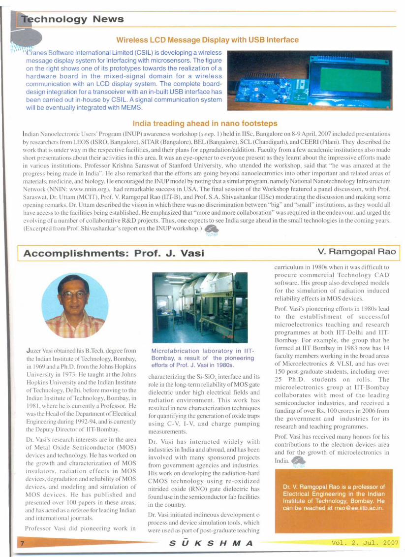
I Wireless LCD Message Display with USB Interface111,1 II I
"""' "t'ranes Software International Limited (CSIL) is developing a wirelessmessage display system for interfacing with microsensors. The figureon the right shows one of its prototypes towards the realization of ahardware board in the mixed-signal domain for a wirelesscommunication with an LCD display system. The complete board-design integration for a transceiver with an in-built USB interface hasbeen carried out in-house by CSIL. A signal communication systemwill be eventually integrated with MEMS.
India treading ahead in nano footstepsIndian Nanoelectronic Users' Program (IN UP) awareness workshop (s eep. I) held in IISc, Bangalore on 8-9 April, 2007 included presentationsby researchers from LEOS (ISRO, Bangalore), SITAR (Bangalore), BEL (Bangalore), SCL(Chandigarh), and CEERI (Pilani). They described thework that is under way in the respective facilities, and their plans for upgradation/addition. Faculty from a few academic institutions also madeshort presentations about their activities in this area. It was an eye-opener to everyone present as they learnt about the impressive efforts madein various institutions. Professor Krishna Saraswat of Stanford University, who 'lttended the workshop, said that "he was amazed at theprogress being made in India". He also remarked that the efforts are going beyond nanoelectronics into other important and related areas ofmaterials, medicine, and biology. He encouraged the lNUP model by noting that a similar program, namely National Nanotechnology InfrastructureNetwork (NNIN: www.nnin.org), had remarkable success in USA. The final session of the Workshop featured a panel discussion, with Prof.Saraswat, Dr. Uttam (MCIT), Prof. V. Ramgopal Rao (lIT-B), and Prof. S.A. Shivashankar (IISc) moderating the discussion and making someopening remarks. Dr. Uttam described the vision in which there was no discrimination between "big" and "small" institutions, as they would allhave access to the facilities being established. He emphasized that "more and more collaboration" was required in the endeavour, and urged theevolving of a number of collaborative R&D projects. Thus, one expects to see India surge ahead in the small technologies in the coming years.(Excerpted from Prof. Shivashankar's report on the INUP workshop.) A
'''~~':,,::,'.,
Juzer Vasi obtained his BTech. degree fromthe Indian Institute of Technology, Bombay,in 1969 and a Ph.D. from the Johns HopkinsUniversity in 1973. He taught at the JohnsHopkins University and the Indian Instituteof Technology, Delhi, before moving to theIndian Institute of Technology, Bombay, in1981, where he is currently a Professor. Hewas the Head of the Department of ElectricalEngineering during 1992-94, and is currentlythe Deputy Director of lIT-Bombay.
Dr. Vasi's research interests are in the areaof Metal Oxide Semiconductor (MOS)devices and technology. He has worked onthe growth and characterization of MOSinsulators, radiation effects in MOSdevices, degradation and reliability ofMOSdevices, and modeling and simulation ofMOS devices. He has published andpresented over 100 papers in these areas,and has acted as a referee for leading Indianand international journals.
Professor Vasi did pioneering work In
Microfabrication laboratory in IIT-Bombay, a result of the pioneeringefforts of Prof. J. Vasi in 1980s.
characterizing the Si-SiOz interface and itsrole in the long-term reliability ofMOS gatedielectric under high electrical fields andradiation environment. This work hasresulted in new characterization techniquesfor quantifying the generation of oxide trapsusing C- V, I-V, and charge pumpingmeasurements.
Dr. Vasi has interacted widely withindustries in India and abroad, and has beeninvolved with many sponsored projectsfrom government agencies and industries.His work on developing the radiation-hardCMOS technology using re-oxidizednitrided oxide (RNO) gate dielectric hasfound use in the semiconductor fab facilitiesin the country.
Dr. Vasi initiated indineous development 0
process and device simulation tools, whichwere used as part of post-graduate teaching
curriculum in 1980s when it was difficult toprocure commercial Technology CADsoftware. His group also developed modelsfor the simulation of radiation inducedreliability effects in MOS devices.
Prof. Vasi's pioneering efforts in 1980s leadto the establishment of successfulmicroelectronics teaching and researchprogrammes at both lIT-Delhi and IlT-Bombay. For example, the group that heformed at lIT Bombay in 1983 now has 14faculty members working in the broad areasof Microelectronics & VLSI, and has over150 post-graduate students, including over25 Ph.D. students on rolls. Themicroelectronics group at IIT-Bombaycollaborates with most of the leadingsemiconductor industries, and received afunding of over Rs. 100 crores in 2006 fromthe government and industries for itsresearch and teaching programmes.
Prof. Vasi has received many honors for hiscontributions to the electron devices areaand for the growth of microelectronics in
India·ft
Dr. V. Ramgopal Rao is a professor ofElectrical Engineering in the IndianInstitute of Technology, Bombay. Hecan be reached at [email protected].
SUKSHMAInstitute of Smart Structures and SystemsDepartment of Aerospace EngineeringIndian Institute of ScienceBangalore - 560012India