CS/EE 6710 Digital VLSI Design -...
51
1 CS/EE 6710 Digital VLSI Design CS/EE 6710 Digital VLSI Design
Transcript of CS/EE 6710 Digital VLSI Design -...

1
CS/EE 6710Digital VLSI Design
CS/EE 6710Digital VLSI Design
2
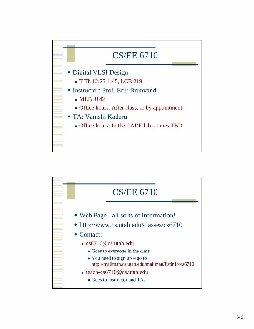
CS/EE 6710
Digital VLSI DesignT Th 12:25-1:45, LCB 219
Instructor: Prof. Erik BrunvandMEB 3142Office hours: After class, or by appointment
TA: Vamshi KadaruOffice hours: In the CADE lab – times TBD
CS/EE 6710
Web Page - all sorts of information!http://www.cs.utah.edu/classes/cs6710Contact:
[email protected] to everyone in the classYou need to sign up – go tohttp://mailman.cs.utah.edu/mailman/listinfo/cs6710
[email protected] to instructor and TAs
3
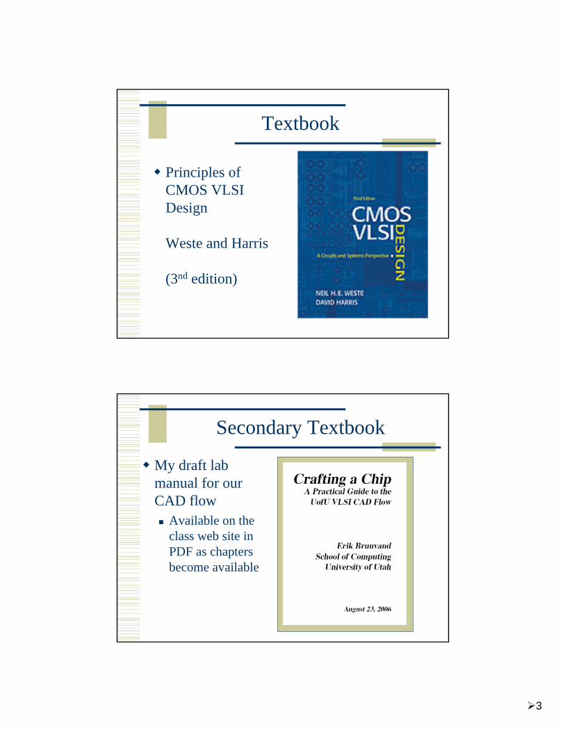
Textbook
Principles of CMOS VLSI Design
Weste and Harris
(3nd edition)
Secondary Textbook
My draft lab manual for our CAD flow
Available on the class web site in PDF as chapters become available
4
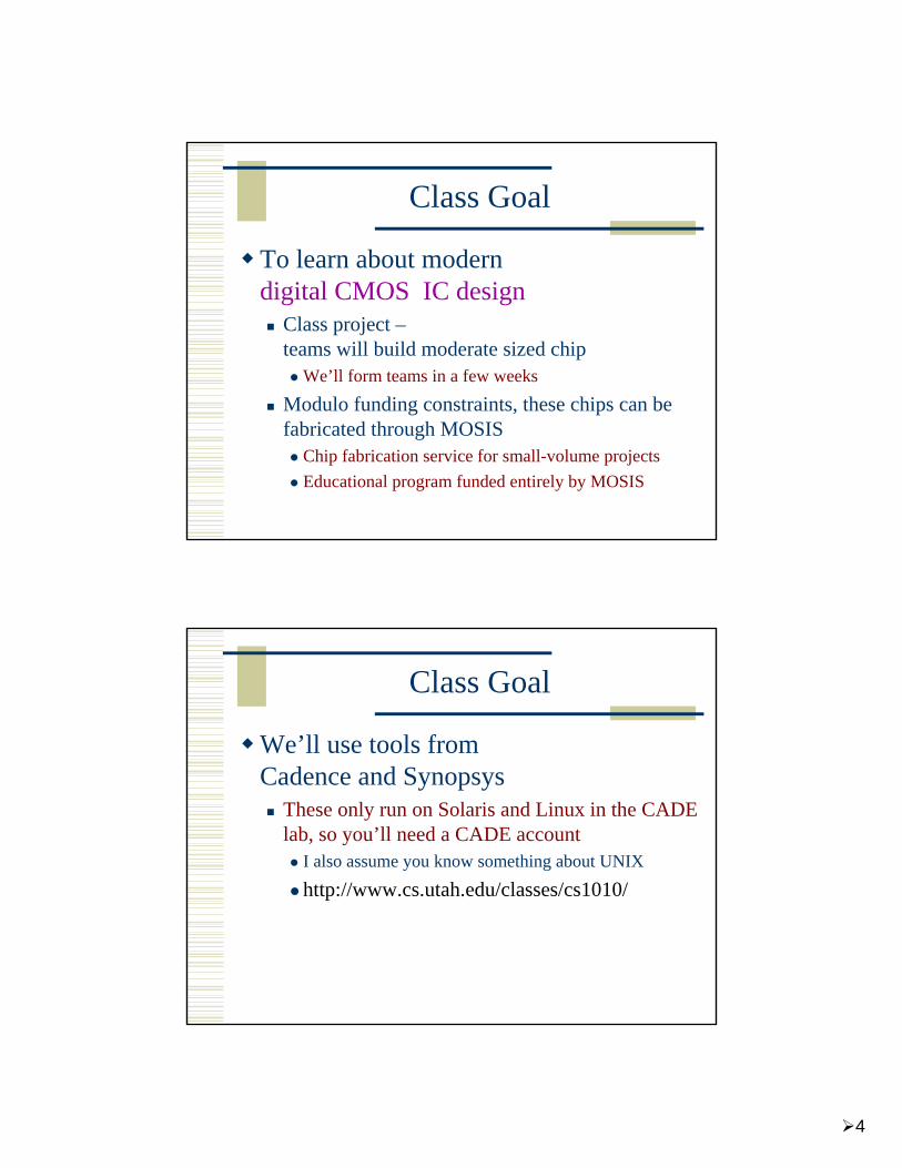
Class Goal
To learn about modern digital CMOS IC design
Class project –teams will build moderate sized chip
We’ll form teams in a few weeks
Modulo funding constraints, these chips can be fabricated through MOSIS
Chip fabrication service for small-volume projectsEducational program funded entirely by MOSIS
Class Goal
We’ll use tools from Cadence and Synopsys
These only run on Solaris and Linux in the CADE lab, so you’ll need a CADE account
I also assume you know something about UNIX
http://www.cs.utah.edu/classes/cs1010/

5
Prerequisites
Digital design is required! (i.e. CS/EE 3700)Boolean algebraCombinational circuit design and optimization
K-map minimization, SOP, POS, DeMorgan, bubble-pushing, etc.Arithmetic circuits, 2’s complement numbers
Sequential Circuit design and optimizationLatch/flip-flop designFinite state machine design/implementationCommunicating FSMsUsing FSMs to control datapaths
Assignment #1 – Review
On the class web site is a review assignmentIf you can do these problems, you probably have the right backgroundIf you can’t, you will struggle!!!!!
Please take this seriously! Give this exam a try and make sure you remember what you need to know!
You also need to turn it in next week by Friday September 1st
Grading is pass/fail

6
Recommendations
Computer Architecture experience is helpfulInstruction set architecture (ISA)Assembly language execution modelInstruction encodingSimple pipelining
I assume you’ve used some sort of CAD tools for digital circuits
Schematic captureSimulation
First Assignment
CAD Assignment #1Cadence Composer tutorialSimple circuit design with simulation
Learn basic Verilog for testbench
Available on the web siteDue on Friday, September 1st, 5:00pm
7
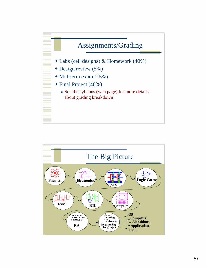
Assignments/Grading
Labs (cell designs) & Homework (40%)Design review (5%)Mid-term exam (15%)Final Project (40%)
See the syllabus (web page) for more details about grading breakdown
The Big Picture
Physics ElectronicsVLSI
Logic Gates
FSM RTLFSM
Computer
MOV R1 R2ADD R1 R3 R5ST R3 (5)R6
ISA
if (c==1)x = foo(y);
elsex = bar(a,b);
ProgammingLanguages
OSCompilersAlgorithms
ApplicationsEtc...

8
Lightening Tour of VLSI Design
Start with HDL program (VHDL, Verilog)entity traffic is
port (CLK, go_green, go_red, go_yellow: in STD_LOGIC;l_green, l_red, l_yellow: out STD_LOGIC;);
end;architecture traffic_arch of traffic is-- SYMBOLIC ENCODED state machine: Sreg0type Sreg0_type is (green, red, yellow);signal Sreg0: Sreg0_type;begin--concurrent signal assignmentsSreg0_machine: process (CLK)beginif CLK'event and CLK = '1' then
case Sreg0 iswhen green =>
if go_yellow='1' thenSreg0 <= yellow;
end if;when red =>
if go_green='1' thenSreg0 <= green;
end if;when yellow =>
if go_red='1' thenSreg0 <= red;
end if;
-- when others =>null;
end case;end if;end process;assignment statements for combinatorial outputs
l_green_assignment:l_green <= '1' when (Sreg0 = green) else
'0' when (Sreg0 = red) else'0' when (Sreg0 = yellow) else'0';
l_yellow_assignment:l_yellow <= '0' when (Sreg0 = green) else
'0' when (Sreg0 = red) else'1' when (Sreg0 = yellow) else'1';
l_red_assignment:l_red <= '0' when (Sreg0 = green) else
'1' when (Sreg0 = red) else'0' when (Sreg0 = yellow) else'0';
end traffic_arch;
VLSI DesignOr start with a schematic (or a mix of both)

9
Convert Gates to Transistors
Convert Transistors to Layout

10
Assemble Gates into a Circuit
And Assemble Whole Chip
11
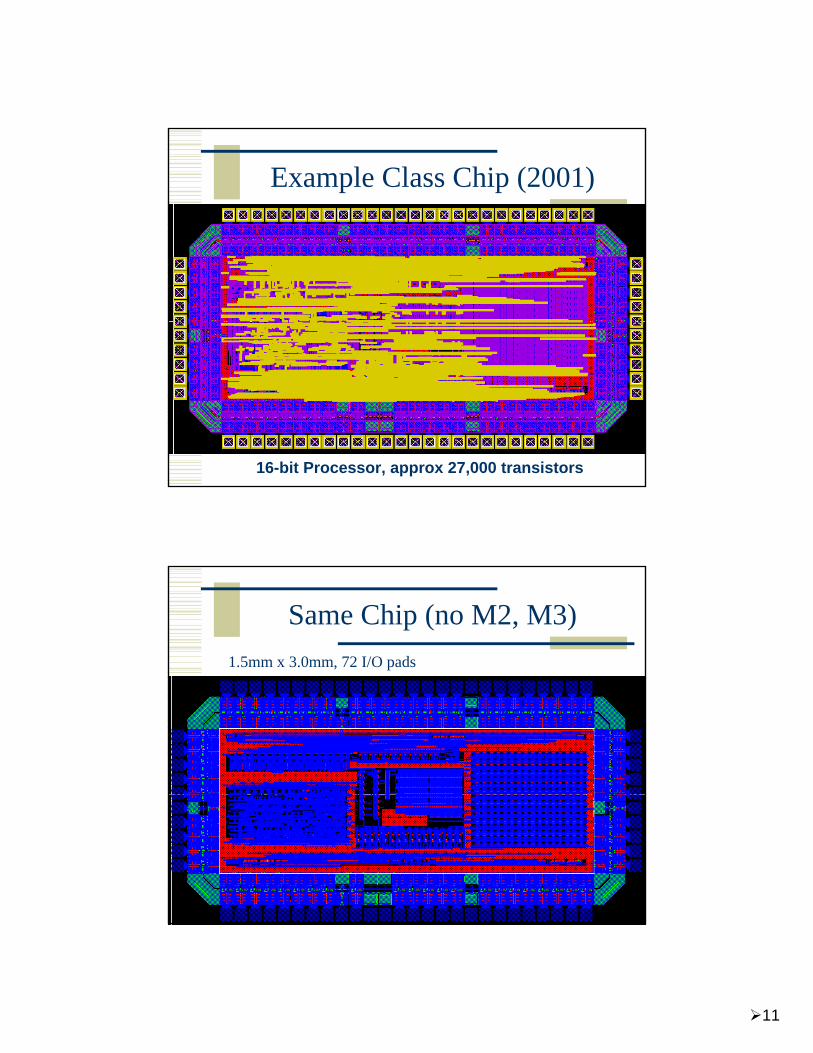
Example Class Chip (2001)
16-bit Processor, approx 27,000 transistors
Same Chip (no M2, M3)1.5mm x 3.0mm, 72 I/O pads

12
Zoom In…
Zoom In…
A Hair (100 microns)
13
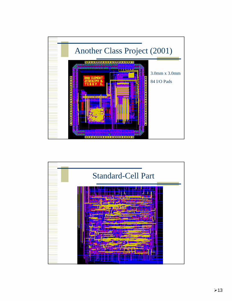
Another Class Project (2001)
3.0mm x 3.0mm
84 I/O Pads
Standard-Cell Part
14
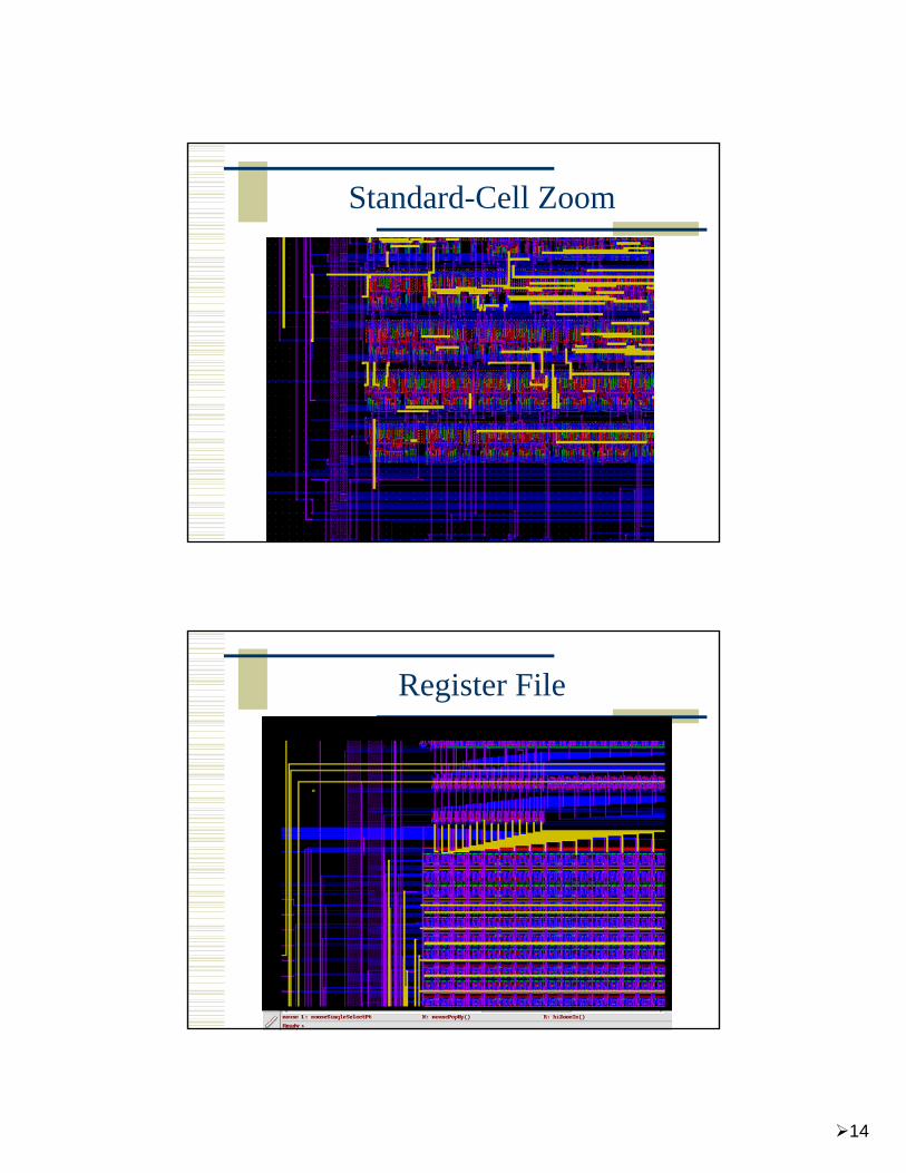
Standard-Cell Zoom
Register File

15
Adder/Shifter
Class project from 2002
16-bit CORDIC Processor
16
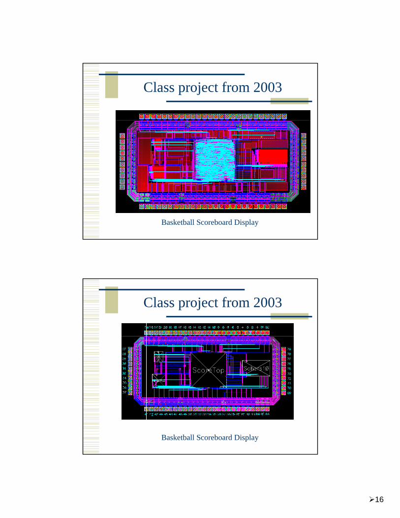
Class project from 2003
Basketball Scoreboard Display
Class project from 2003
Basketball Scoreboard Display
17
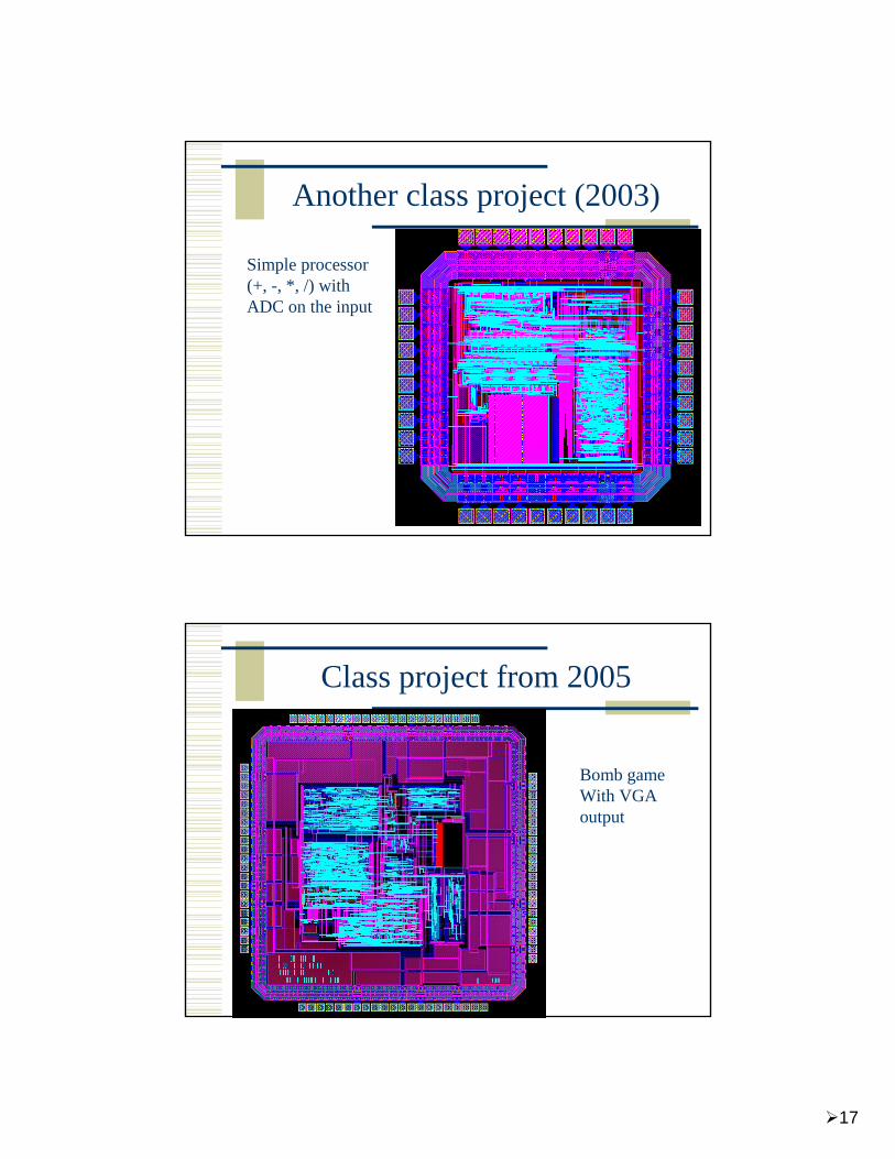
Another class project (2003)
Simple processor (+, -, *, /) with ADC on the input
Class project from 2005
Bomb gameWith VGA output

18
Bomb game from 2005
Bomb game from 2005
19
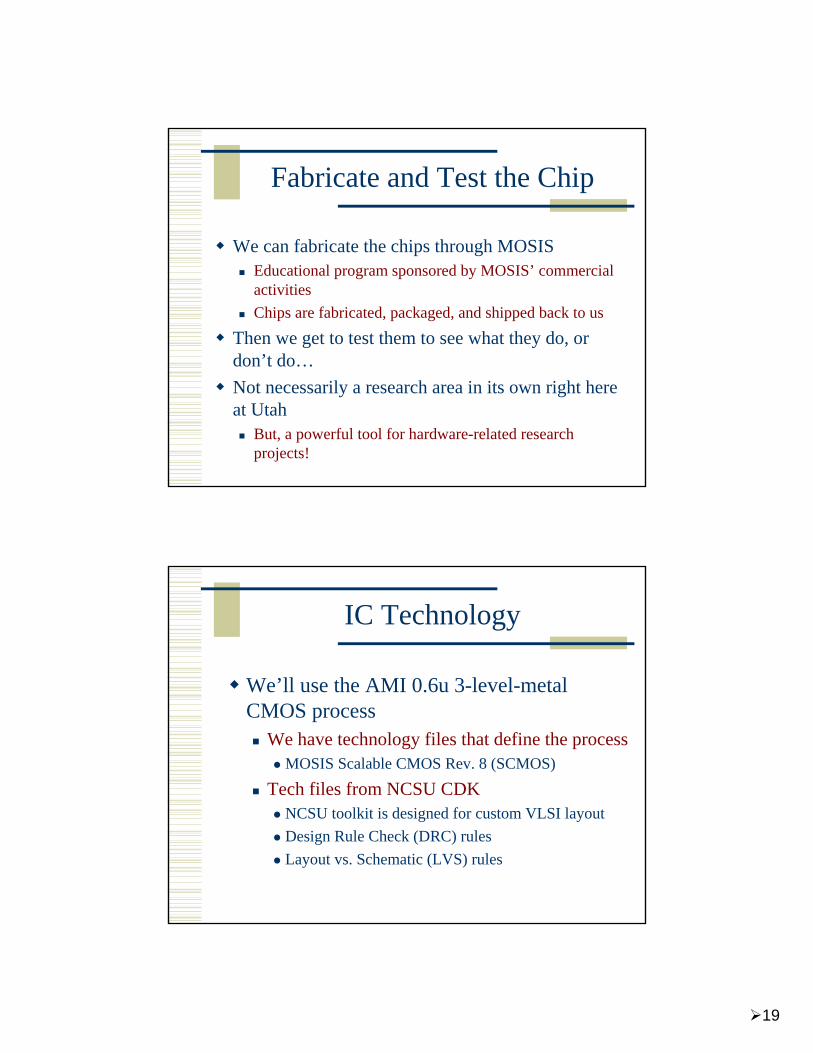
Fabricate and Test the Chip
We can fabricate the chips through MOSISEducational program sponsored by MOSIS’ commercial activitiesChips are fabricated, packaged, and shipped back to us
Then we get to test them to see what they do, or don’t do… Not necessarily a research area in its own right here at Utah
But, a powerful tool for hardware-related research projects!
IC Technology
We’ll use the AMI 0.6u 3-level-metal CMOS process
We have technology files that define the processMOSIS Scalable CMOS Rev. 8 (SCMOS)
Tech files from NCSU CDKNCSU toolkit is designed for custom VLSI layoutDesign Rule Check (DRC) rulesLayout vs. Schematic (LVS) rules

20
Class Project
Standard Cell LibraryEach group will design a small, but useful, standard cell library
Use HDL synthesis with this library as a targetUse Cadence SOC Encounter for place and route
Custom Datapath Use ICC router to connect HDL-Synthesized control to custom-designed datapathIt will be VERY helpful to have a mix of knowledge on your team
Class Project Two complete design views:Schematic and Layout
Complete design in Composer schematics, simulated with VerilogComplete design at layout level in Virtuoso with detailed simulation using SpectreValidate they are the same with LVS
Custom layout for datapathSynthesized controller using Synopsys, SOC Encounter, and your cell libraryFinal assembly back in Virtuoso

21
Timetable
This project will be a race to the finish!There is no slack in this schedule!!!
VLSI design always takes longer than you thinkEven if you take that rule into account!
After you have 90% finished, there’s only 90% left…
All team members will have to contribute!Team peer evaluations twice a semester
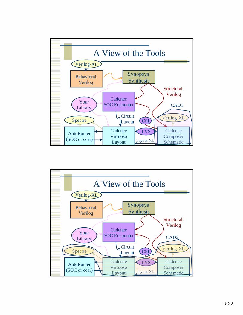
A View of the Tools
Synopsys Synthesis
CadenceSOC Encounter
CadenceComposerSchematic
CadenceVirtuosoLayout
AutoRouter(SOC or ccar)
YourLibrary
Verilog-XL
Verilog-XL
BehavioralVerilog
Structural Verilog
CircuitLayout
LVS
Layout-XL
CSISpectre
22
A View of the Tools
Synopsys Synthesis
CadenceSOC Encounter
CadenceComposerSchematic
CadenceVirtuosoLayout
AutoRouter(SOC or ccar)
YourLibrary
Verilog-XL
Verilog-XL
BehavioralVerilog
Structural Verilog
CircuitLayout
LVS
Layout-XL
CSISpectre
CAD1
A View of the Tools
Synopsys Synthesis
CadenceSOC Encounter
CadenceComposerSchematic
CadenceVirtuosoLayout
AutoRouter(SOC or ccar)
YourLibrary
Verilog-XL
Verilog-XL
BehavioralVerilog
Structural Verilog
CircuitLayout
LVS
Layout-XL
CSISpectre
CAD2

23
Cadence Composer Schematic
Cadence Composer Schematic

24
Cadence Composer Symbol
Cadence Virtuoso Layout
25
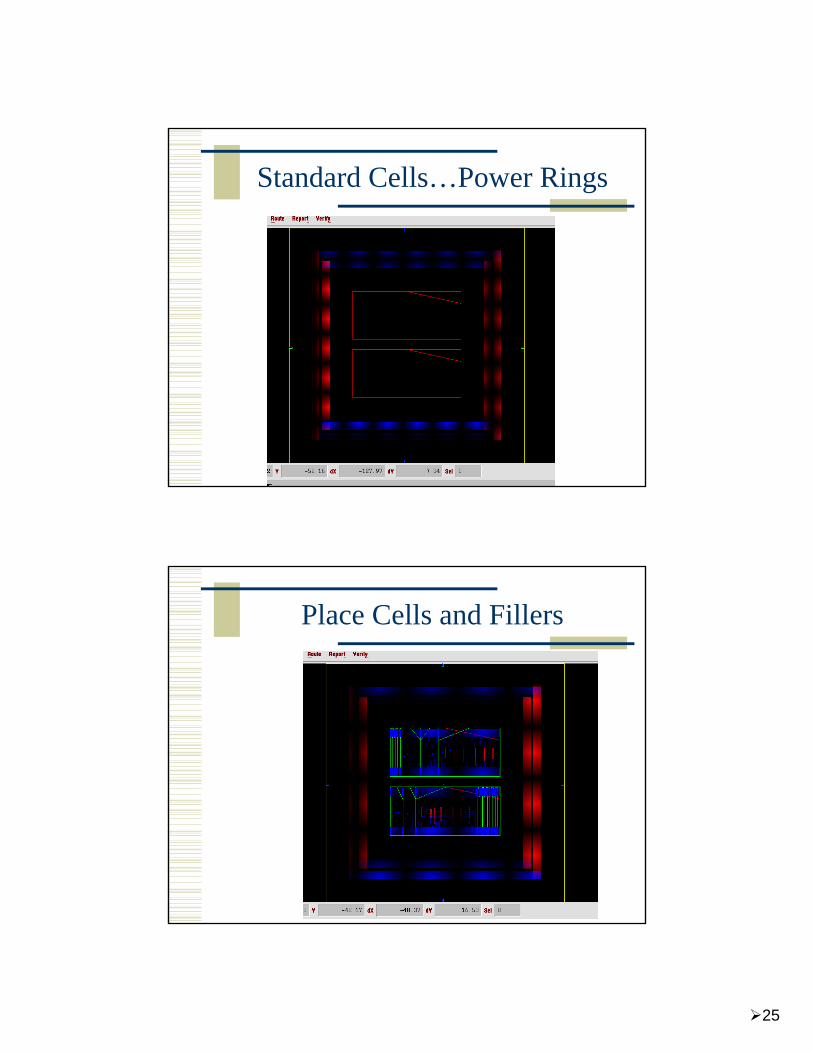
Standard Cells…Power Rings
Place Cells and Fillers
26
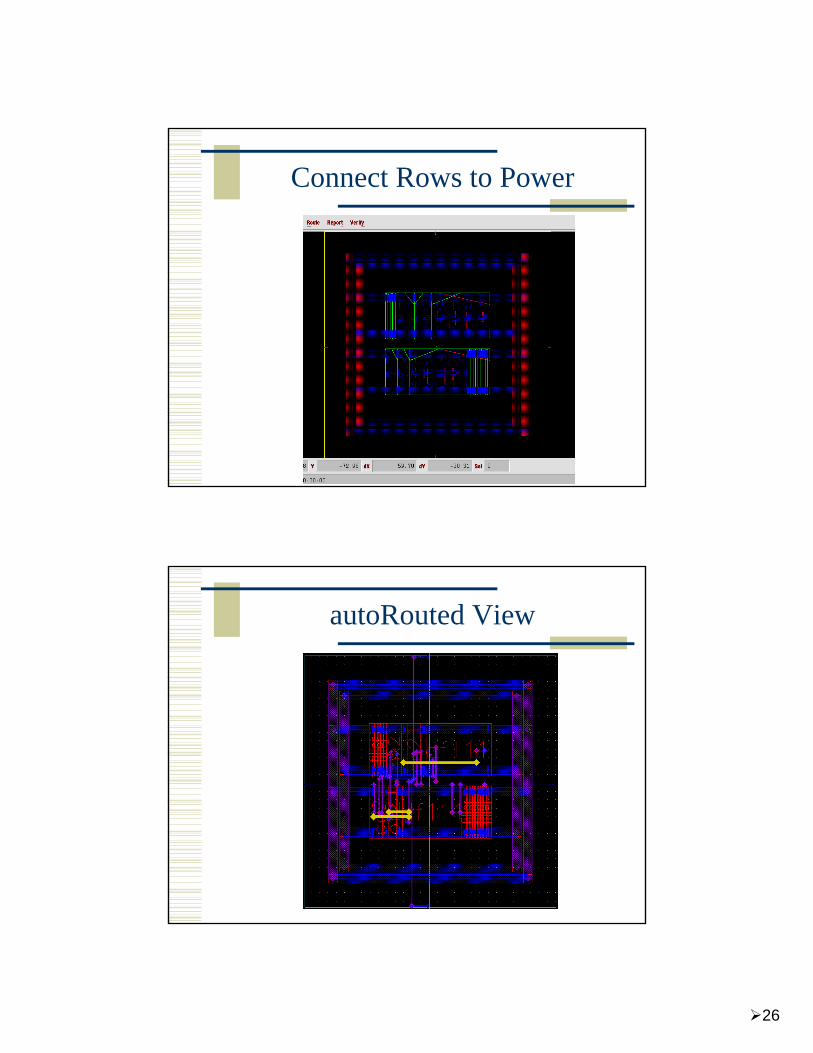
Connect Rows to Power
autoRouted View
27
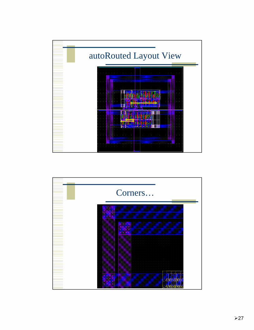
autoRouted Layout View
Corners…
28
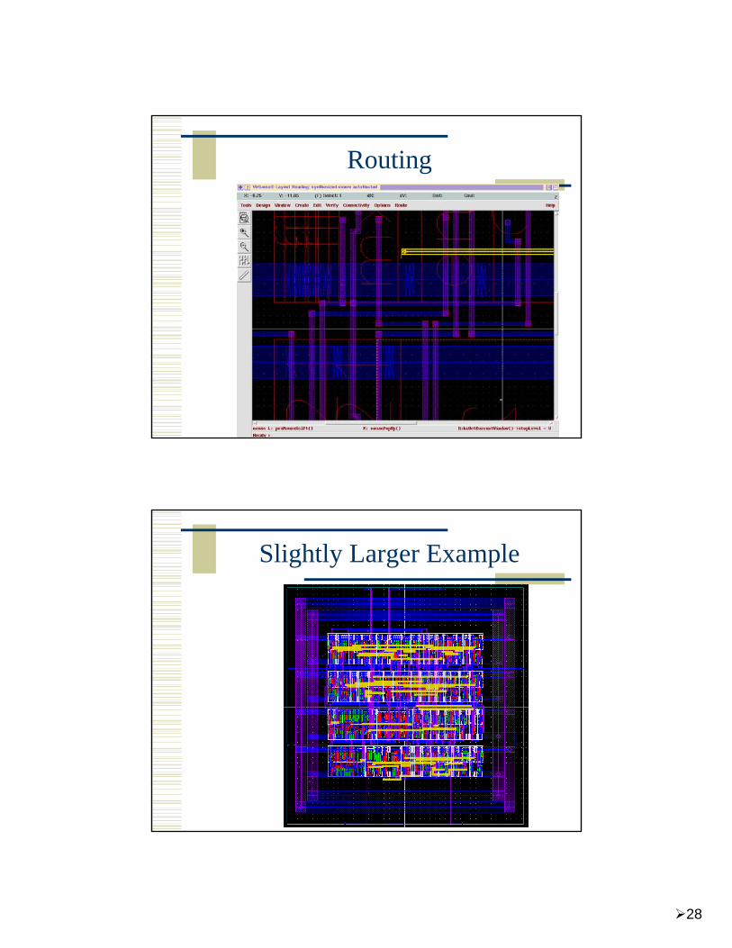
Routing
Slightly Larger Example

29
Electronics SummaryVoltage is a measure of electrical potential energy
Current is moving charge caused by voltage
Resistance reduces current flowOhm’s Law: V = I R
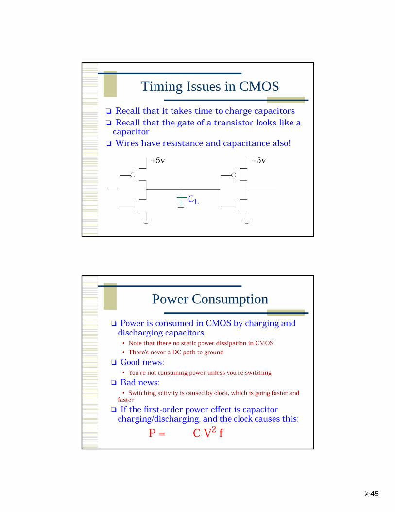
Power is work over timeP = V I = I2R = V2/R
Capacitors store chargeIt takes time to charge/ discharge a capacitorTime to charge/discharge is related exponentially to RCIt takes energy to charge a capacitorEnergy stored in a capacitor is (1/2)CV2
Energy (joules): work required to move one coulomb of charge by one volt or work done to produce one watt for one sec
Reminder: Voltage Division
Find the voltage across any series-connected resistors

30
Example of Voltage Division
Find the voltage at point A with respect to GND
Example of Voltage Division
Find the voltage at point A with respect to GND

31
How Does This Relate to VLSI?
Model of a CMOS Transistor

32
Two Types of CMOS Transistors
CMOS Transistors
Complementary Metal Oxide SemiconductorTwo types of transistors
Built on silicon substrate“majority carrier” devicesField-effect transistors
An electric field attracts carriers to form a conducting channel in the silicon…We’ll get much more of this later… For now, just some basic abstractions

33
Silicon Lattice
Transistors are built on a silicon substrateSilicon is a Group IV materialForms crystal lattice with bonds to four neighbors
Figures from Reid Harrison
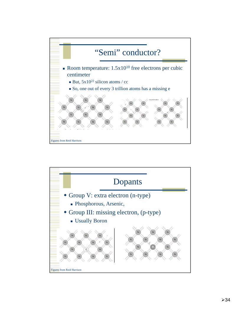
“Semi” conductor?
Thermal energy (atomic-scale vibrations) can shake an electron loose
Leaves a “hole” behind
Figures from Reid Harrison
34
“Semi” conductor?
Room temperature: 1.5x10¹⁰ free electrons per cubic centimeter
But, 5x10²² silicon atoms / ccSo, one out of every 3 trillion atoms has a missing e
Figures from Reid Harrison
DopantsGroup V: extra electron (n-type)
Phosphorous, Arsenic, Group III: missing electron, (p-type)
Usually Boron
Figures from Reid Harrison
35
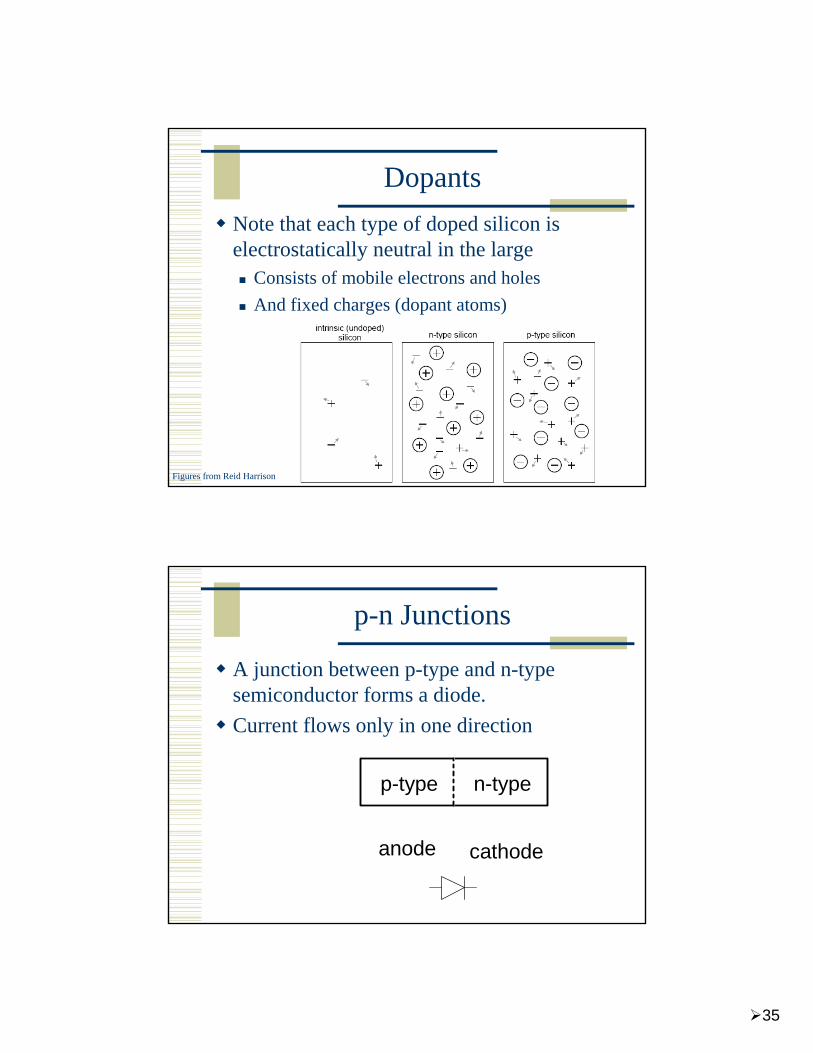
DopantsNote that each type of doped silicon is electrostatically neutral in the large
Consists of mobile electrons and holesAnd fixed charges (dopant atoms)
Figures from Reid Harrison
p-n Junctions
A junction between p-type and n-type semiconductor forms a diode.Current flows only in one direction
p-type n-type
anode cathode

36
p-n Junctions
Two mechanisms for carrier (hole or electron) motion
Drift - requires an electric fieldDiffusion – requires a concentration gradient
Figures from Reid Harrison
p-n Junctions
With no external voltage diffusion causes a depletion region
Causes anelectric fieldbecause ofcharge recombination
Causes driftcurrent…
Figures from Reid Harrison

37
p-n Junctions
Eventually reaches equilibrium where diffusion current offsets drift current
Figures from Reid Harrison
p-n Junctions
By applying an external voltage you can modulate the width fo the depletion region and cause diffusion or drift to dominate…
Figures from Reid Harrison

38
+
-
i electronsVds
+Vgs S
G
D
N-type Transistor
nMOS Operation
Body is commonly tied to ground (0 V)When the gate is at a low voltage:
P-type body is at low voltageSource-body and drain-body diodes are OFFNo current flows, transistor is OFF
n+
p
GateSource Drain
bulk Si
SiO2
Polysilicon
n+D
0
S

39
nMOS Operation Cont.
When the gate is at a high voltage:Positive charge on gate of MOS capacitorNegative charge attracted to bodyInverts a channel under gate to n-typeNow current can flow through n-type silicon from source through channel to drain, transistor is ON
n+
p
GateSource Drain
bulk Si
SiO2
Polysilicon
n+D
1
S
+
-
i holesVsd-Vgs S
G
D
P-type Transistor

40
pMOS Transistor
Similar, but doping and voltages reversedBody tied to high voltage (VDD)Gate low: transistor ONGate high: transistor OFFBubble indicates inverted behavior
SiO2
n
GateSource Drain
bulk Si
Polysilicon
p+ p+
A Cutaway View
CMOS structure with both transistor types

41
Transistors as Switches
For now, we’ll abstract away most analog details…
S
G
D
S
G
D
G=0 G=1
G=0 G=1
Good 0
Poor 0 Good 1
Poor 1
Good 1
Good 0 Good 1
Good 0
Not Perfect Switches!
“Switching Circuit”
For example, a switch can control when a light comes on or off
No electricity can flow
+5v
0v

42
“AND” Circuit
Both switch X AND switch Y need to be closed for the light to light up
+5v
0vX Y
“OR” Circuit
The light comes on if either X OR Y are closed
+5v
X
Y 0v

43
CMOS Inverter
CMOS Inverter
10
YA VDD
A Y
GNDA Y
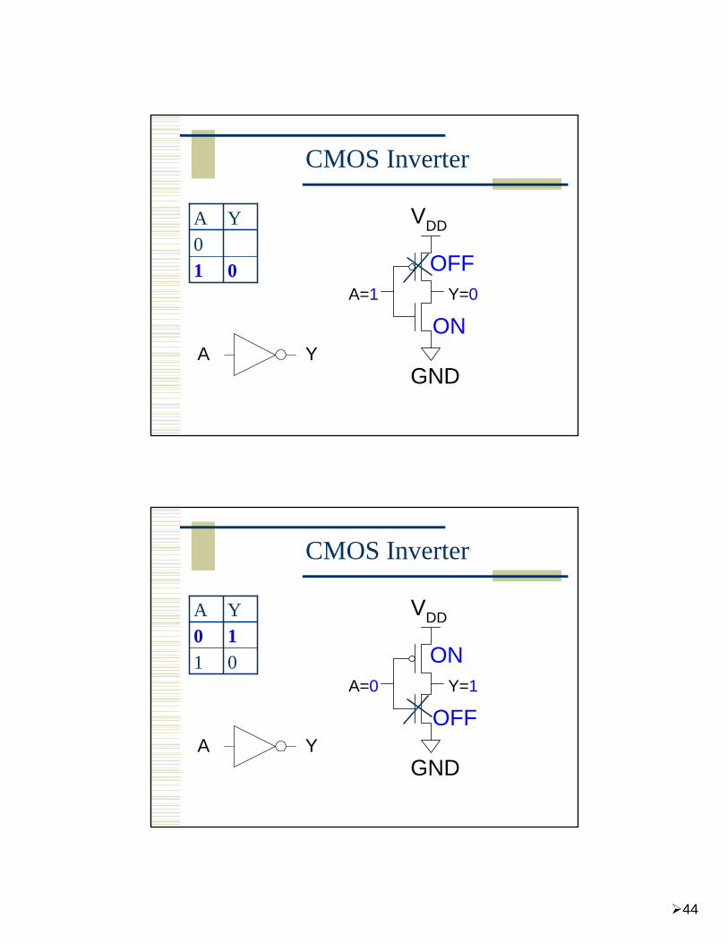
44
CMOS Inverter
010
YA VDD
A=1 Y=0
GND
ON
OFF
A Y
CMOS Inverter
0110YA VDD
A=0 Y=1
GND
OFF
ON
A Y
45
Timing Issues in CMOS
Power Consumption
46
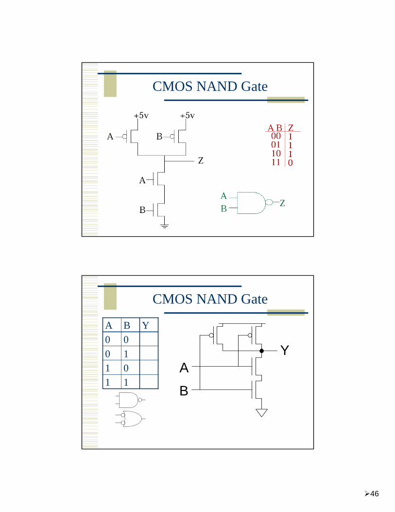
CMOS NAND Gate
CMOS NAND Gate
1100A
101
0YB
A
B
Y
47
CMOS NAND Gate
1100A
101
10YB
A=0
B=0
Y=1OFF
ON ON
OFF
CMOS NAND Gate
1100A
1101
10YB
A=0
B=1
Y=1OFF
OFF ON
ON

48
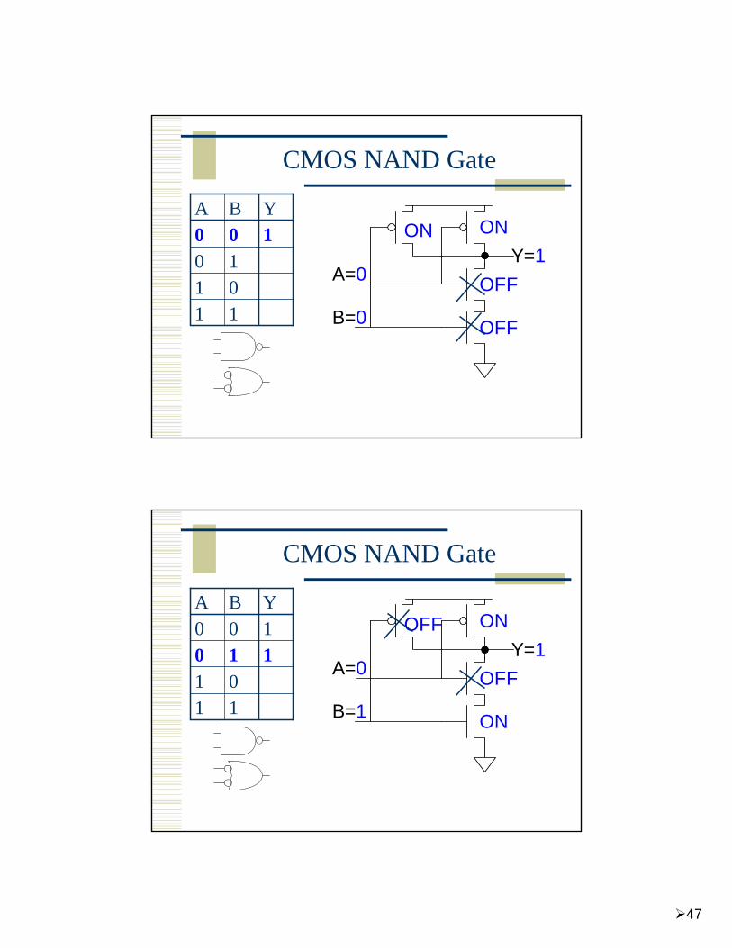
CMOS NAND Gate
1100A
1110
1
10YB
A=1
B=0
Y=1ON
ON OFF
OFF
CMOS NAND Gate
1100A
111001
10YB
A=1
B=1
Y=0ON
OFF OFF
ON
49
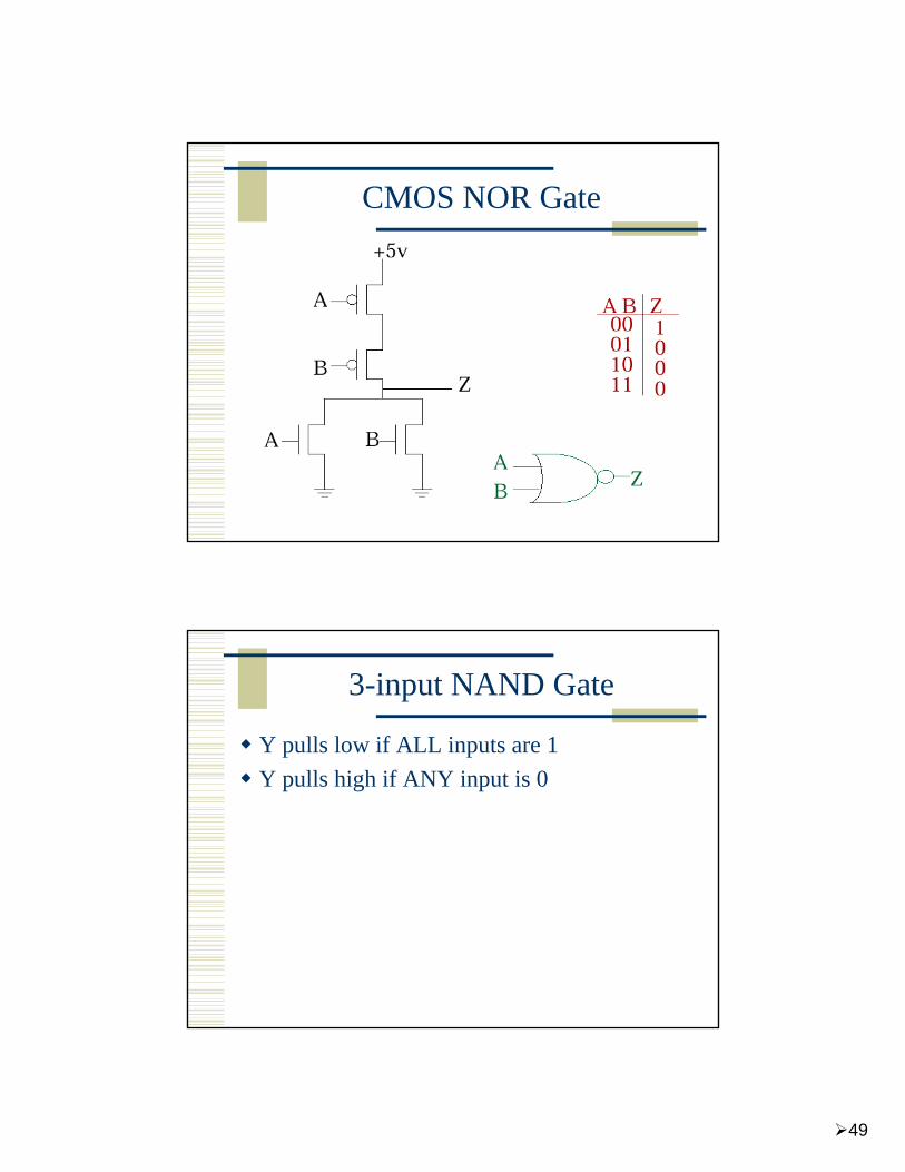
CMOS NOR Gate
3-input NAND Gate
Y pulls low if ALL inputs are 1Y pulls high if ANY input is 0

50
3-input NAND Gate
Y pulls low if ALL inputs are 1Y pulls high if ANY input is 0
AB
Y
C
N-type and P-type Uses
Because of the imperfect nature of the the transistor switches
ALWAYS use N-type to pull lowALWAYS use P-type to pull highIf you need to pull both ways, use them both
S
In
Out
SS=0, In = OutS=1, In = Out
51
Switch to Chalkboard
Complex GateTri-StateLatchD-registerXOR