
CS/EE 6710 CMOS Processing. N-type Transistor + - i electrons Vds +Vgs S G D.
61
CS/EE 6710 CMOS Processing
-
Upload
roberta-hawkins -
Category
Documents
-
view
225 -
download
2
Transcript of CS/EE 6710 CMOS Processing. N-type Transistor + - i electrons Vds +Vgs S G D.
CS/EE 6710
CMOS Processing

N-type Transistor
+
-
i electronsVds
+Vgs S
G
D
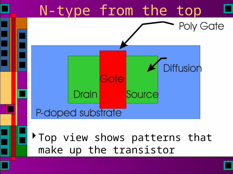
N-type from the top
Top view shows patterns that make up the transistor
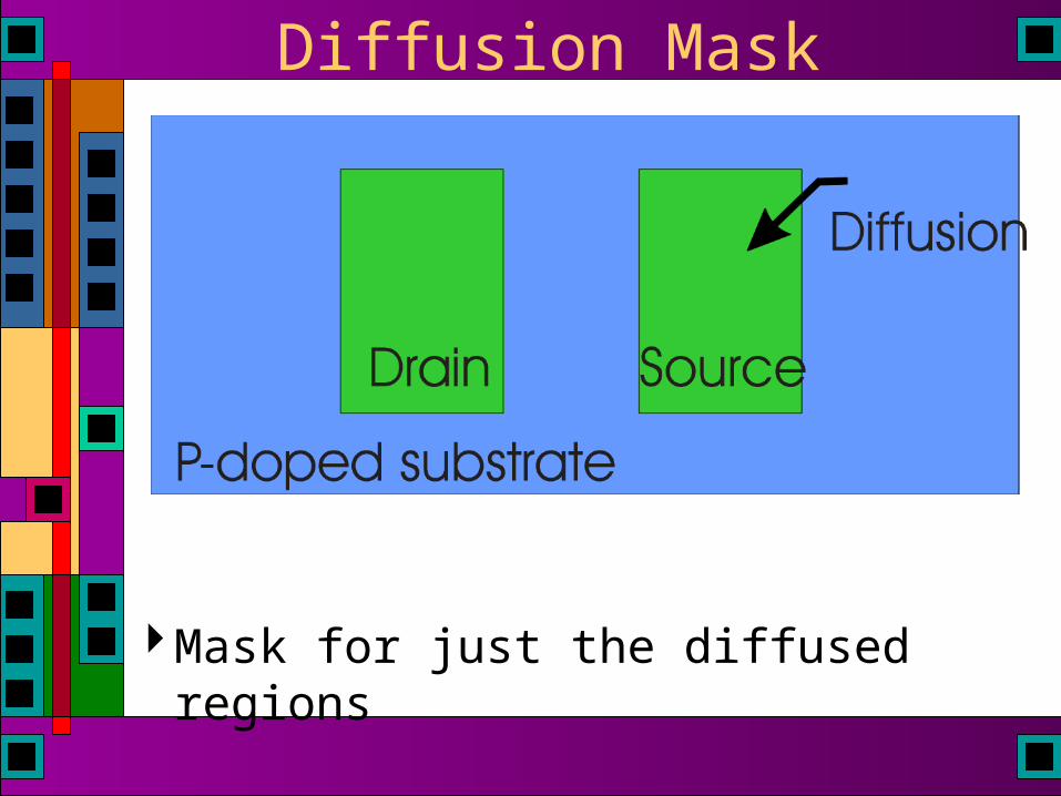
Diffusion Mask
Mask for just the diffused regions
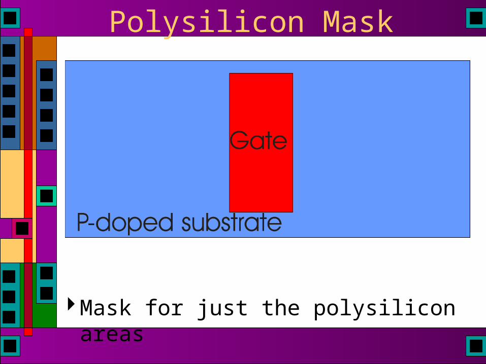
Polysilicon Mask
Mask for just the polysilicon areas

Combine the two masks
You get an N-type transistorThere are other steps in the process…

A Cutaway View
CMOS structure with both transistor types

Look at Inverter Layout Again
How many layers?How many processing steps?

Photolithography Oxidation LayerPhotoresist (PR)
CoatingStepper ExposurePR development and
bakeAcid EtchingSpin, Rinse, DryProcessing stepPR removal (ashing)
UV Light

Photolithographic Process

Photolithographic Process
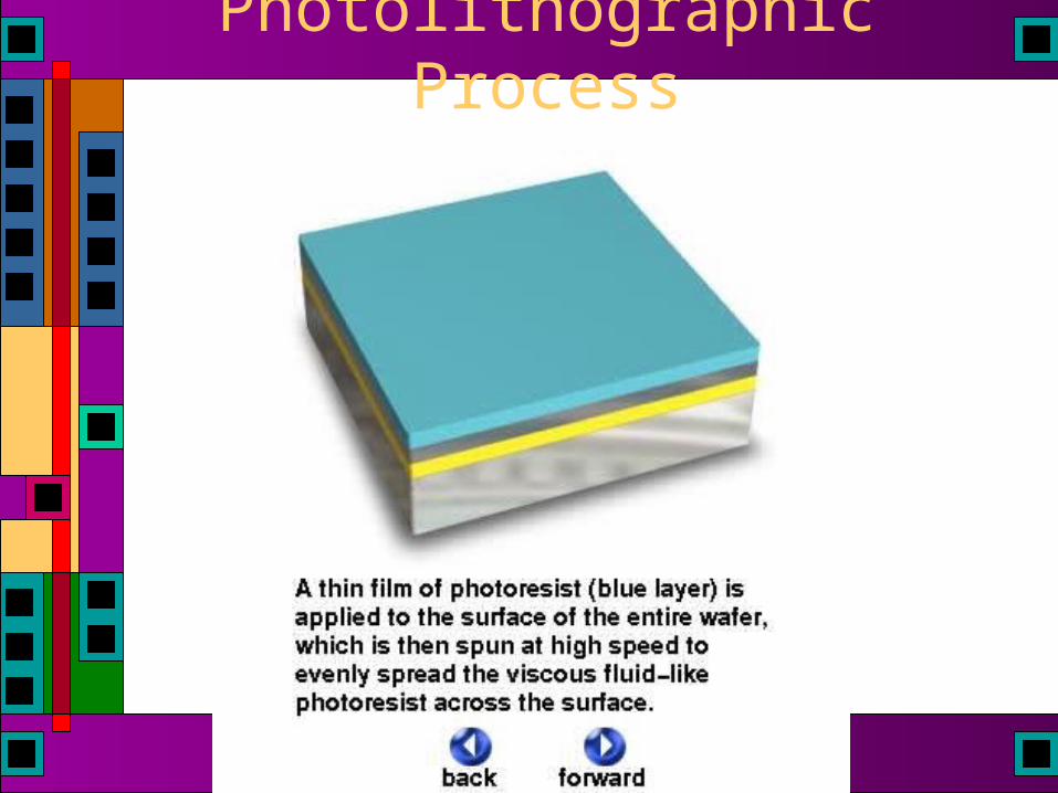
Photolithographic Process

Photolithographic Process

Photolithographic Process

Photolithographic Process

Photolithographic Process

Growing the Silicon Crystal
Need single crystal structure Single crystal vs. Polycrystalline silicon (Poly)

Czochralski Method
Need single-crystal silicon to accept impurities correctlyDonor elements provide electronsAcceptor elements provide holes
Pull a single crystal of silicon from a puddle of molten polycrystalline silicon

Slice Crystal into Wafers
Slice into thin wafers (.25mm - 1.0mm), and polish to remove all scratches

Lapping and Polishing

Oxidation, Growing SiO2
Essential property of silicon is a nice, easily grown, insulating layer of SiO2Use for insulating gates (“thin oxide”)Also for “field oxide” to isolate devices

Making the Mask
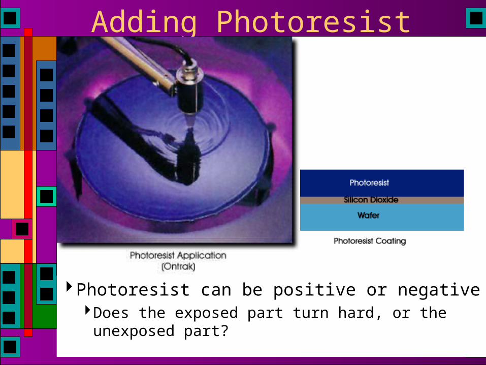
Adding Photoresist
Photoresist can be positive or negativeDoes the exposed part turn hard, or the unexposed
part?

“Steppers” Expose the Mask
Use very short wavelength UV lightSingle frequency, 436 - 248 nm
Expensive! ~$5,000,000/machine…

Develop and Bake Photoresist
Developed photoresist is soft, unexposed is hardened So you can etch away the soft (exposed) part

Now Etch the SiO2
Etch the SiO2 to expose the wafer for processing
Then Spin Rinse, and Dry

Add a Processing Step
Now that we’ve got a pattern etched to the right level, we can process the silicon
Could be:Ion Implantation (I.e. diffusion)Chemical Vapor Deposition (silicide, Poly,
insulating layers, etc.)Metal deposition (evaporation or sputtering)Copper deposition (very tricky)

Ion Implantation
Implant ions into the siliconDonor or Acceptor
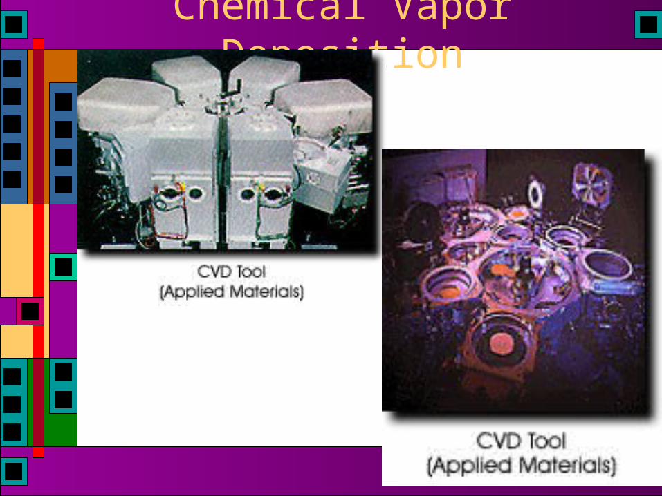
Chemical Vapor Deposition

Metal Deposition
Typically aluminum, gold, tungsten, or alloys
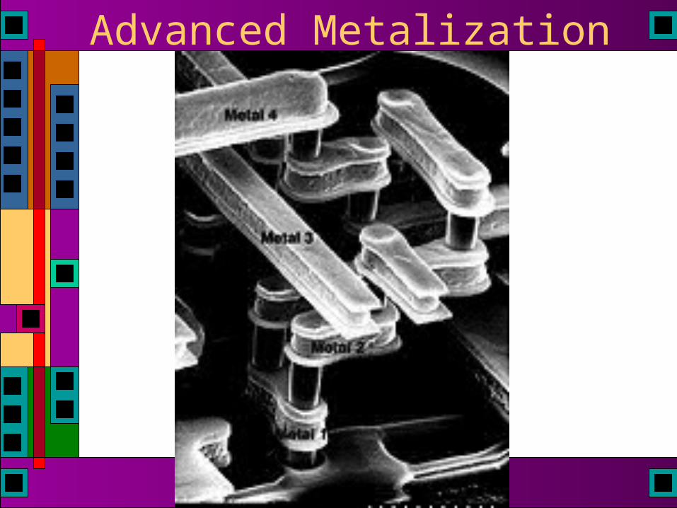
Advanced Metalization

Copper is Tricky
40% less resistance than Aluminum 15% system speed increase
But, copper diffuses into Silicon and changes the electrical properties

Ashing - Removing Photoresist
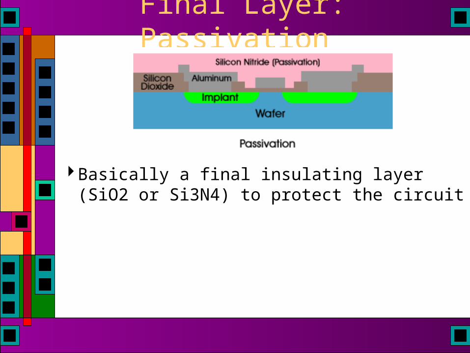
Final Layer: Passivation
Basically a final insulating layer (SiO2 or Si3N4) to protect the circuit
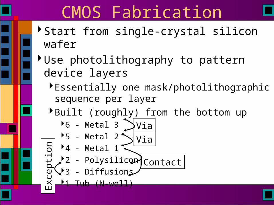
CMOS FabricationStart from single-crystal silicon waferUse photolithography to pattern device layers
Essentially one mask/photolithographic sequence per layer
Built (roughly) from the bottom up6 - Metal 35 - Metal 24 - Metal 12 - Polysilicon3 - Diffusions1 Tub (N-well)
Exc
eptio
n
Contact
Via
Via

Self-Aligned GatesThinox in active
regions, thick elsewhere
Deposit Polysilicon
Etch thinox from active region (Poly serves as mask for etch/diffusion)
Implant dopant

CMOS Inverter
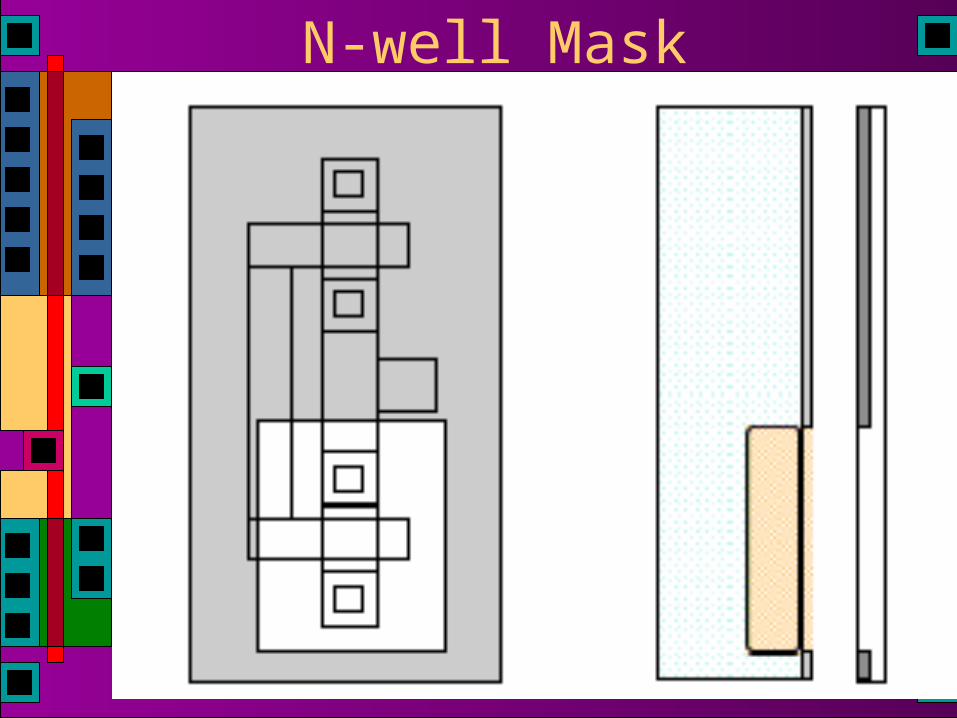
N-well Mask
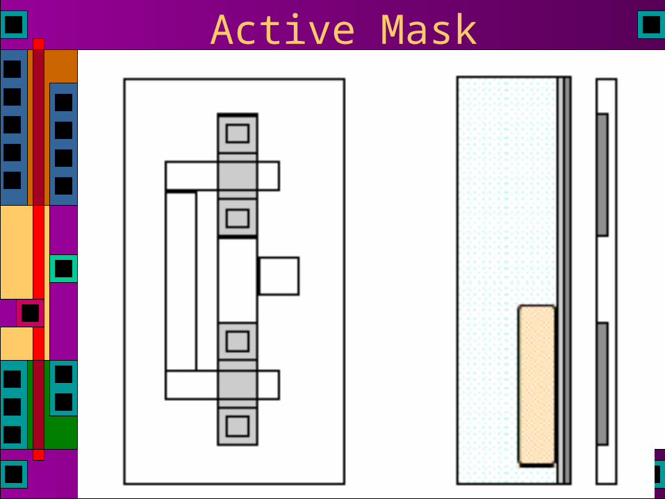
Active Mask
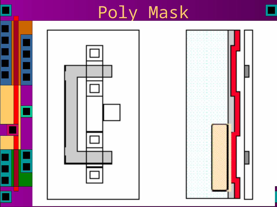
Poly Mask

N+ Select Mask

P+ Select Mask

Contact Mask

Metal Mask

Other Cutaway Views

Another View of Fab
Taken from slides by Jan RabaeyFrom his text “Digital Integrated Circuits”
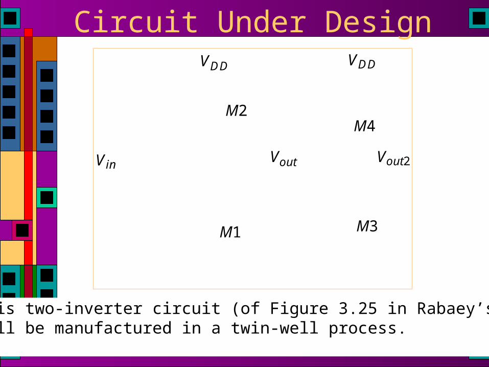
Circuit Under Design
This two-inverter circuit (of Figure 3.25 in Rabaey’s text )will be manufactured in a twin-well process.
VDD VDD
Vin Vout
M1
M2
M3
M4
Vout2
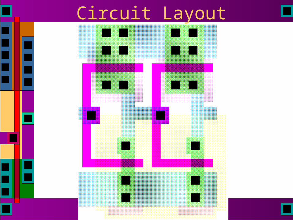
Circuit Layout

Start Material
Starting wafer: n-type withdoping level = 10 13/cm3
* Cross-sections will be shown along vertical line A-A’
A
A’

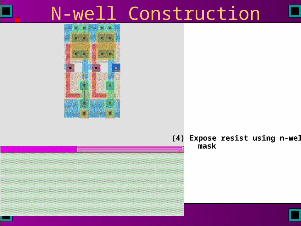
N-well Construction
(1) Oxidize wafer(2) Deposit silicon nitride(3) Deposit photoresist
N-well Construction
(4) Expose resist using n-wellmask

N-well Construction
(5) Develop resist(6) Etch nitride and(7) Grow thick oxide

N-well Construction
(8) Implant n-dopants (phosphorus)
(up to 1.5 m deep)

P-well Construction
Repeat previous steps
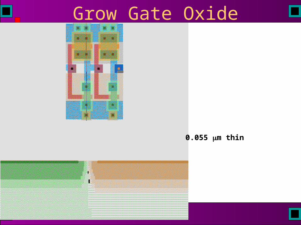
Grow Gate Oxide
0.055 m thin

Grow Thick Field Oxide
Uses Active Area mask
Is followed by threshold-adjusting implants
0.9 m thick

Polysilicon layer

Source-Drain Implants
n+ source-drain implant(using n+ select mask)
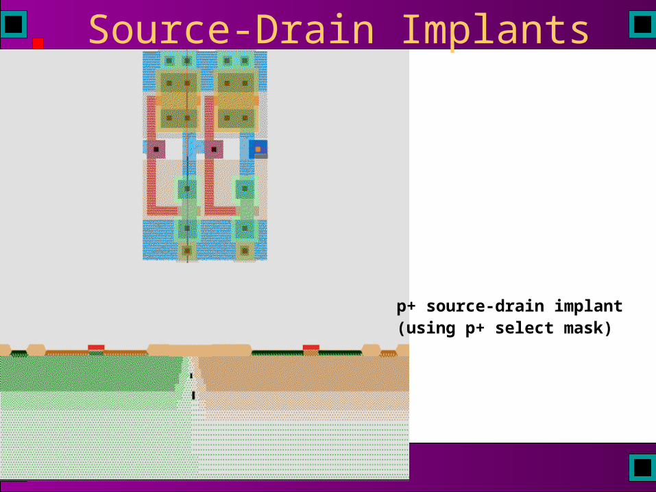
Source-Drain Implants
p+ source-drain implant(using p+ select mask)

Contact-Hole Definition
(1) Deposit inter-level dielectric (SiO2) — 0.75 m
(2) Define contact opening using contact mask

Aluminum-1 Layer
Aluminum evaporated (0.8 m thick)
followed by other metal layers and glass
![[MS-VDS]: Virtual Disk Service (VDS) Protocol... · [MS-VDS]: Virtual Disk Service (VDS) Protocol Intellectual Property Rights Notice for Open Specifications Documentation](https://static.fdocuments.in/doc/165x107/5ece0e4751b19024473b3e8c/ms-vds-virtual-disk-service-vds-protocol-ms-vds-virtual-disk-service.jpg)