Csc1401 lecture06 - internal memory
34
Madam Raini Hassan Office: C5 - 23, Level 5, KICT Building Department: Computer Science Emails: [email protected], [email protected] 1
-
Upload
pocong-makenon -
Category
Education
-
view
105 -
download
1
Transcript of Csc1401 lecture06 - internal memory

Madam Raini Hassan
Office: C5 - 23, Level 5, KICT Building
Department: Computer Science
Emails: [email protected], [email protected] 1

Du’a for Study
Semester II 2014/2015 2

LECTURE 06
Internal Memory (Chapter 5)

Outline
• Semiconductor Main
Memory
Organization
DRAM and SRAM
Types of ROM
Chip Logic
Chip Packaging
Module Organization
Interleaved Memory
• Error Correction
• Advanced DRAM
Organization
Synchronous DRAM
Rambus DRAM
DDR SDRAM
Cache DRAM
Semester II 2014/2015 4

5
Organization: Memory Cell
• The basic element of semiconductor memory.
• Properties:
– They exhibit two stable (or semi-stable) states, which can be
used to represent binary 1 and 0.
– They capable of being written into (at least one) to set the
state.
– They are capable of being read to sense the data.
Semester II 2014/2015

6
Organization: Memory Cell
Operation • The select terminal selects a memory cell for a read or
write operation.
• The control terminal indicated read or write.
Semester II 2014/2015

Semiconductor Memory Types
Table 5.1 Semiconductor Memory Types
The most common is referred to as Random-access Memory (RAM).
7
8
Semiconductor Memory: RAM
• Misnamed as all semiconductor memory is random
access.
• Possible for both Read/Write operation
• Volatile – once the power supply is interrupted, the data
will be lost
• Used for temporary storage
• Has 2 types:
– Dynamic
– Static
Semester II 2014/2015

9
Semiconductor Memory: DRAM
• Constructed by an array of cells, each cell containing 1
transistor and a tiny capacitor.
• These cells store data as charge in capacitors - presence or
absence of charge in a capacitor is interpreted as a binary 1
or 0
• Charges leak; the term dynamic refers to the tendency of
stored charge to leak away even with power continuously
applied.
• Requires periodic charge refreshing to maintain data storage
• The term dynamic refers to tendency of the stored charge to
leak away, even with power continuously applied
• Simpler construction
Semester II 2014/2015

10
Semiconductor Memory: DRAM
• Smaller per bit
• Less expensive
• Need refresh circuits
• Slower
• Used for main memory
• Essentially analogue
– The capacitor can store any charge value within a range; level of charge determines value
Semester II 2014/2015

11
Semiconductor Memory: DRAM Op
• Address line active when bit read or
written
– The transistor acts as a switch that is closed
(allow current to flow) if a voltage is
applied to the address line and open (no
current flow) if no voltage is present on
the address line.
• Write Operation:
– Voltage to bit line
– High voltage = 1; low voltage = 0
– A signal is then applied to the address line
– allowing a charge to be transferred to the
capacitor Semester II 2014/2015

12
Semiconductor Memory: DRAM Op
• Read Operation:
– When address line selected
• transistor turns on
– Charge from capacitor fed via bit line
to sense amplifier
• Sense amplifiers compares capacitor
voltage with reference value to
determine 0 or 1
– Capacitor charge must be restored to
complete the operation.
Semester II 2014/2015

13
Semiconductor Memory: SRAM
• Bits stored as on/off switches
• No charges to leak & no refreshing needed when powered
• More complex construction & larger per bit
• Does not need refresh circuits
• Faster and more expensive
• Used for cache
• Will hold its data as long as power is supplied to it.
• Digital – a digital device, using the same logic elements used
in the processor
– Uses flip-flops – traditional flip-flop logic-gate
configuration. Semester II 2014/2015

14
Semiconductor Memory: SRAM Op
• Transistor arrangement gives stable logic state (T1..T4)
• In logic State 1 – C1 high, C2 low and T1 T4 off, T2 T3 on
• In logic State 0 – C2 high, C1 low andT2 T3 off, T1 T4 on
• Address line transistors T5 T6 is switch – when on, allowing a read/write operation
• Write – apply value to B & compliment to B
• Read – value is on line B
Semester II 2014/2015

SRAM versus DRAM • Both volatile
Power must be continuously supplied to the memory to preserve the bit
values
• Dynamic cell
Simpler to build, smaller
More dense (smaller cells = more cells per unit area)
Less expensive
Requires the supporting refresh circuitry
Tend to be favored for large memory requirements
Used for main memory
• Static
Faster
Used for cache memory (both on and off chip)
Semester II 2014/2015 15

Semiconductor Memory: ROM
• Contains a permanent pattern of data that cannot be changed or added to
• No power source is required to maintain the bit values in memory
• Data or program is permanently in main memory and never needs to be loaded from a secondary storage device
• Data is actually wired into the chip as part of the fabrication process
– Disadvantages of this:
• No room for error, if one bit is wrong the whole batch of ROMs must be thrown out
• Data insertion step includes a relatively large fixed cost
Semester II 2014/2015 16

Semiconductor Memory: Types of
ROM - PROM
• Stands for Programmable ROM
• Less expensive alternative
• Nonvolatile and may be written into only once
• Writing process is performed electrically and may be
performed by supplier or customer at a time later than
the original chip fabrication
• Special equipment is required for the writing process
• Provides flexibility and convenience
• Attractive for high volume production runs
Semester II 2014/2015 17

Semiconductor Memory: Types of
ROM -Read-Mostly Memory
EPROM
Erasable programmable read-only memory
Erasure process can be performed repeatedly
More expensive than PROM but it has the advantage of
the multiple update capability
EEPROM
Electrically erasable programmable read-only
memory
Can be written into at any time without erasing prior
contents
Combines the advantage of non-volatility with the
flexibility of being updatable in place
More expensive than EPROM
Flash Memory
Intermediate between EPROM and EEPROM in both cost and functionality
Uses an electrical erasing technology, does not provide
byte-level erasure
Microchip is organized so that a section of memory cells are erased in a single
action or “flash”
18

• A 16Mbit chip can be organized as 1M of 16 bit words
• A bit per chip system has 16 lots of 1Mbit chip with bit 1 of
each word in chip 1 and so on
• A 16Mbit chip can be organized as a 2048 x 2048 x 4 bit
array
– Reduces number of address pins
– Multiplex row address and column address
– 11 pins to address (211=2048)
– Adding one more pin doubles range of values so x4 capacity
Chip Logic
Semester II 2014/2015 19

Chip Logic:
Typical 16 Mb DRAM (4M x 4)
20

Chip Packaging
Semester II 2014/2015 21

Mo
du
le O
rgan
izatio
n
Memory address
register (MAR)
256K, 8-bit word
8 pieces of
256K ×1-bit chip
22
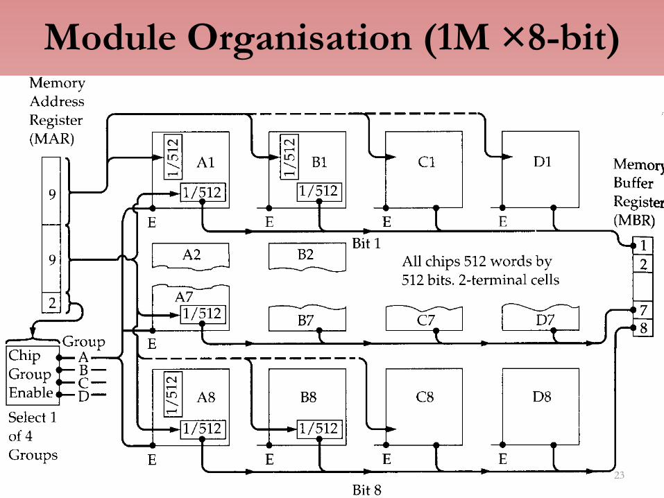
Module Organisation (1M ×8-bit)
23

Interleaved Memory Composed of a collection of DRAM chips.
Grouped together to form a memory bank.
Each bank is independently able to service a memory read or write request.
K banks can service K requests simultaneously, increasing memory read or write rates by a factor of K.
If consecutive words of memory are stored in different banks, the transfer of a block of memory is speeded up.
Semester II 2014/2015 24

25
Error Correction • A semiconductor memory is subject to errors. 2
categories:
• Hard Failure
– Permanent physical defect so that the memory cell/cells affected cannot reliably store data but become stuck at 0 or 1 or switch erratically between 0 and 1.
• Soft Error
– Random, non-destructive events that alters the contents of one or memory cells.
– No permanent damage to memory.
– Can be caused by power supply problem.
Semester II 2014/2015
Semester II 2014/2015 26
Error Correction
• Both are not desirable, and most modern main memory
have systems include logic for both detecting and
correcting errors.
• The simplest of the error-correcting codes is the
Hamming code.

27
Error Correction: Error-
Correcting Code Function
1. When data are to be read into
memory, a calculation depicted as
a function f is performed on the
data to produce a code.
2. Both the code and the data are
stores, thus if an M-bit word of
data is to be stored, and the code
is of length K bits, then the actual
size of the stored word in M + K
bits.
3. When the previously stored
word is read out, the code is used
to detect and possibly correct
errors. Semester II 2014/2015

28
Error Correction: Error-
Correcting Code Function 4. A new set of K code bits is generated from the M data bits and compared with the fetched bits.
5. The comparison yields one of the 3 results:
– No errors are detected. The fetched data bits are sent out.
– An error is detected, and it is possible to correct the error. The data bits plus error correction bits are fed into a corrector, which produces a corrected set of M bits to be sent out.
– An error is detected, but it is not possible to correct it. This condition is reported.
6. A code is characterized by the number of bits errors in a word that it can correct and detect.
Semester II 2014/2015

Error
Correction:
Hamming
Error
Correcting
Code
29

Advanced DRAM Organization
• One of the most critical system bottlenecks when using high-performance processors is the interface to main internal memory
• The traditional DRAM chip is constrained both by its internal architecture and by its interface to the processor’s memory bus
• A number of enhancements to the basic DRAM architecture have been explored:
Table 5.3 Performance Comparison of Some DRAM Alternatives 30

Synchronous DRAM (SDRAM)
One of the most widely used forms of DRAM
Exchanges data with the processor synchronized to an external clock signal and running at the full
speed of the processor/memory bus without imposing wait states
With synchronous access the DRAM moves data in and out under control of the system clock
• The processor or other master issues the instruction and address information which is latched by the DRAM
• The DRAM then responds after a set number of clock cycles
• Meanwhile the master can safely do other tasks while the SDRAM is processing
31

RDRAM Developed by Rambus
Adopted by Intel for its Pentium and Itanium processors
Has become the main competitor to SDRAM
Chips are vertical packages with all pins on one side
• Exchanges data with the processor over 28 wires no more than 12 centimeters long
Bus can address up to 320 RDRAM chips and is rated at 1.6 GBps
Bus delivers address and control information using an asynchronous block-oriented protocol
• Gets a memory request over the high-speed bus
• Request contains the desired address, the type of operation, and the number of bytes in the operation
32

Double Data Rate SDRAM
(DDR SDRAM)
• SDRAM can only send data once per bus clock cycle
• Double-data-rate SDRAM can send data twice per clock
cycle, once on the rising edge of the clock pulse and once
on the falling edge
• Developed by the JEDEC Solid State Technology
Association (Electronic Industries Alliance’s
semiconductor-engineering-standardization body)
Semester II 2014/2015 33

Cache DRAM (CDRAM)
• Developed by Mitsubishi
• Integrates a small SRAM cache onto a generic DRAM
chip
• SRAM on the CDRAM can be used in two ways:
– It can be used as a true cache consisting of a number of 64-
bit lines
• Cache mode of the CDRAM is effective for ordinary random access
to memory
– Can also be used as a buffer to support the serial access of a
block of data
Semester II 2014/2015 34