CS61C L20 Single Cycle Datapath, Control (1) Chae, Summer 2008 © UCB Albert Chae, Instructor...
50
CS61C L20 Single Cycle Datapath, Control (1) Chae, Summer 2008 © UCB Albert Chae, Instructor inst.eecs.berkeley.edu/~cs61c CS61C : Machine Structures Lecture #20 – Single Cycle CPU Datapath and Control 2008-7-24
-
date post
22-Dec-2015 -
Category
Documents
-
view
215 -
download
0
Transcript of CS61C L20 Single Cycle Datapath, Control (1) Chae, Summer 2008 © UCB Albert Chae, Instructor...

CS61C L20 Single Cycle Datapath, Control (1) Chae, Summer 2008 © UCB
Albert Chae, Instructor
inst.eecs.berkeley.edu/~cs61c CS61C : Machine Structures
Lecture #20 – Single Cycle CPU Datapath and Control
2008-7-24

CS61C L20 Single Cycle Datapath, Control (2) Chae, Summer 2008 © UCB
Review• CPU design involves Datapath,Control
• Datapath in MIPS involves 5 CPU stages
1) Instruction Fetch
2) Instruction Decode & Register Read
3) ALU (Execute)
4) Memory
5) Register Write

CS61C L20 Single Cycle Datapath, Control (3) Chae, Summer 2008 © UCB
Single Cycle CPU
• Single Cycle CPU: All stages of an instruction are completed within one long clock cycle.
• The clock cycle is made sufficient long to allow each instruction to complete all stages without interruption and within one cycle.
For each instruction, how do we control the flow of information though the datapath?
1. InstructionFetch
2. Decode/ Register
Read
3. Execute 4. Memory5. Reg. Write

CS61C L20 Single Cycle Datapath, Control (4) Chae, Summer 2008 © UCB
How to Design a Processor: step-by-step1. Analyze instruction set architecture (ISA)
=> datapath requirements• meaning of each instruction is given by the register transfers
• datapath must include storage element for ISA registers
• datapath must support each register transfer
2. Select set of datapath components and establish clocking methodology
3. Assemble datapath meeting requirements4. Analyze implementation of each instruction to determine setting of control points that effects the register transfer.
5. Assemble the control logic

CS61C L20 Single Cycle Datapath, Control (5) Chae, Summer 2008 © UCB
Step 3: Assemble DataPath meeting requirements
• Register Transfer Requirements Datapath Assembly
• Instruction Fetch
• Read Operands and Execute Operation
CS61C L20 Single Cycle Datapath, Control (6) Chae, Summer 2008 © UCB
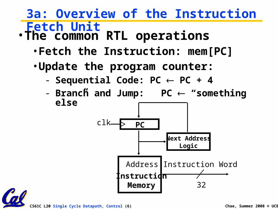
3a: Overview of the Instruction Fetch Unit
• The common RTL operations• Fetch the Instruction: mem[PC]• Update the program counter:
- Sequential Code: PC PC + 4 - Branch and Jump: PC “something else”
32
Instruction WordAddress
InstructionMemory
PCclk
Next AddressLogic

CS61C L20 Single Cycle Datapath, Control (7) Chae, Summer 2008 © UCB
3b: Add & Subtract• R[rd] = R[rs] op R[rt] Ex.: addU rd,rs,rt
• Ra, Rb, and Rw come from instruction’s Rs, Rt, and Rd fields
• ALUctr and RegWr: control logic after decoding the instruction
32Result
ALUctr
clk
busW
RegWr
32
32
busA
32
busB
5 5 5
Rw Ra Rb
32 32-bitRegisters
Rs RtRd
AL
U
op rs rt rd shamt funct061116212631
6 bits 6 bits5 bits5 bits5 bits5 bits
Already defined the register file & ALU

CS61C L20 Single Cycle Datapath, Control (8) Chae, Summer 2008 © UCB
Clocking Methodology
• Storage elements clocked by same edge• Being physical devices, flip-flops (FF) and
combinational logic have some delays • Gates: delay from input change to output change • Signals at FF D input must be stable before active clock
edge to allow signal to travel within the FF (set-up time), and we have the usual clock-to-Q delay
• “Critical path” (longest path through logic) determines length of clock period
Clk
.
.
.
.
.
.
.
.
.
.
.
.

CS61C L20 Single Cycle Datapath, Control (9) Chae, Summer 2008 © UCB
Register-Register Timing: One complete cycleClk
PCRs, Rt, Rd,Op, Func
ALUctr
Instruction Memory Access Time
Old Value New Value
RegWr Old Value New Value
Delay through Control Logic
busA, BRegister File Access TimeOld Value New Value
busWALU Delay
Old Value New Value
Old Value New Value
New ValueOld Value
Register WriteOccurs Here
32
ALUctr
clk
busW
RegWr
32busA
32
busB
5 5
Rw Ra Rb
RegFile
Rs Rt
AL
U
5Rd

CS61C L20 Single Cycle Datapath, Control (10) Chae, Summer 2008 © UCB
3c: Logical Operations with Immediate• R[rt] = R[rs] op ZeroExt[imm16] ]
op rs rt immediate
016212631
6 bits 16 bits5 bits5 bits
immediate
016 1531
16 bits16 bits
0 0 0 0 0 0 0 0 0 0 0 0 0 0 0 0
32
ALUctr
clk
busW
RegWr
32busA
32
busB
5 5
Rw Ra Rb
RegFile
Rs RtA
LU
5Rd
But we’re writing to Rt register??

CS61C L20 Single Cycle Datapath, Control (11) Chae, Summer 2008 © UCB
3c: Logical Operations with Immediate• R[rt] = R[rs] op ZeroExt[imm16] ]
op rs rt immediate
016212631
6 bits 16 bits5 bits5 bits
immediate
016 1531
16 bits16 bits
0 0 0 0 0 0 0 0 0 0 0 0 0 0 0 0
• Already defined 32-bit MUX; Zero Ext?
What about Rt register read??
32
ALUctr
clk
RegWr
32
32busA
32
busB
5 5
Rw Ra Rb
RegFile
Rs
Rt
Rt
Rd
ZeroE
xt 3216imm16
ALUSrc
01
0
1
AL
U
5
RegDst

CS61C L20 Single Cycle Datapath, Control (12) Chae, Summer 2008 © UCB
3d: Load Operations• R[rt] = Mem[R[rs] + SignExt[imm16]]Example: lw rt,rs,imm16
op rs rt immediate
016212631
6 bits 16 bits5 bits5 bits
32
ALUctr
clk
RegWr
32
32busA
32
busB
5 5
Rw Ra Rb
RegFile
Rs
Rt
Rt
Rd
ZeroE
xt 3216imm16
ALUSrc
01
0
1
AL
U
5
RegDst

CS61C L20 Single Cycle Datapath, Control (13) Chae, Summer 2008 © UCB
3d: Load Operations• R[rt] = Mem[R[rs] + SignExt[imm16]]Example: lw rt,rs,imm16
op rs rt immediate
016212631
6 bits 16 bits5 bits5 bits
32
ALUctr
clk
busW
RegWr
32
32busA
32
busB
5 5
Rw Ra Rb
RegFile
Rs
Rt
Rt
RdRegDst
Exten
der 3216imm16
ALUSrcExtOp
MemtoReg
clk
Data In
32
MemWr01
0
1
AL
U 0
1
WrEn Adr
DataMemory
5
?

CS61C L20 Single Cycle Datapath, Control (14) Chae, Summer 2008 © UCB
3e: Store Operations• Mem[ R[rs] + SignExt[imm16] ] = R[rt]
Ex.: sw rt, rs, imm16
op rs rt immediate016212631
6 bits 16 bits5 bits5 bits
32
ALUctr
clk
busW
RegWr
32
32busA
32
busB
5 5
Rw Ra Rb
RegFile
Rs
Rt
Rt
RdRegDst
Exten
der 3216imm16
ALUSrcExtOp
MemtoReg
clk
Data In
32
MemWr01
0
1
AL
U 0
1
WrEn Adr
DataMemory
5

CS61C L20 Single Cycle Datapath, Control (15) Chae, Summer 2008 © UCB
3e: Store Operations• Mem[ R[rs] + SignExt[imm16] ] = R[rt]
Ex.: sw rt, rs, imm16
op rs rt immediate016212631
6 bits 16 bits5 bits5 bits
32
ALUctr
clk
busW
RegWr
32
32busA
32
busB
5 5
Rw Ra Rb
RegFile
Rs
Rt
Rt
RdRegDst
Exten
der 3216imm16
ALUSrcExtOp
MemtoReg
clk
Data In
32
MemWr01
0
1
AL
U 0
1
WrEn Adr
DataMemory
5

CS61C L20 Single Cycle Datapath, Control (16) Chae, Summer 2008 © UCB
3f: The Branch Instruction
beq rs, rt, imm16• mem[PC] Fetch the instruction from memory
• Equal = R[rs] == R[rt] Calculate branch condition
• if (Equal) Calculate the next instruction’s address- PC = PC + 4 + ( SignExt(imm16) x 4 )
else- PC = PC + 4
op rs rt immediate016212631
6 bits 16 bits5 bits5 bits

CS61C L20 Single Cycle Datapath, Control (17) Chae, Summer 2008 © UCB
Datapath for Branch Operations• beq rs, rt, imm16
Datapath generates condition (equal)
op rs rt immediate016212631
6 bits 16 bits5 bits5 bits
Already have mux, adder, need special sign extender for PC, need equal compare (sub?)imm16
clk
PC
00
4nPC_sel
PC
Ext
Ad
derA
dder
Mu
x
Inst Address
32
ALUctr
clk
busW
RegWr
32busA
32
busB
5 5
Rw Ra Rb
RegFile
Rs Rt
AL
U
5
=
Equal

CS61C L20 Single Cycle Datapath, Control (18) Chae, Summer 2008 © UCB
Putting it All Together:A Single Cycle Datapath
imm16
32
ALUctr
clk
busW
RegWr
32
32busA
32
busB
5 5
Rw Ra Rb
RegFile
Rs
Rt
Rt
RdRegDst
Exten
der
3216imm16
ALUSrcExtOp
MemtoReg
clk
Data In32
MemWrEqual
Instruction<31:0><21:25>
<16:20>
<11:15>
<0:15>
Imm16RdRtRs
clk
PC
00
4
nPC_sel
PC
Ext
Adr
InstMemory
Ad
derA
dder
Mu
x
01
0
1
=
AL
U 0
1
WrEn Adr
DataMemory
5

CS61C L20 Single Cycle Datapath, Control (19) Chae, Summer 2008 © UCB
Peer Instruction
A. For the CPU designed so far, the Controller only needs to look at opcode/funct and Equal
B. Adding jal would only require changing the Instruction Fetch block
C. Making our single-cycle CPU multi-cycle will be easy
ABC0: FFF1: FFT2: FTF3: FTT4: TFF5: TFT6: TTF7: TTT

CS61C L20 Single Cycle Datapath, Control (20) Chae, Summer 2008 © UCB
Administrivia
• HW4 Due Friday 7/25• Cut out problem 8
• HW5 out tonight, due next Tuesday 7/29
• HW1,2 Grade Freeze• Submit appeals by Friday 7/25

CS61C L20 Single Cycle Datapath, Control (21) Chae, Summer 2008 © UCB
An Abstract View of the Implementation
DataOut
clk
5
Rw Ra Rb
RegisterFile
Rd
Data In
DataAddr Ideal
DataMemory
Instruction
InstructionAddress
IdealInstruction
Memory
PC
5Rs
5Rt
32
323232
A
B
Nex
t A
dd
ress
Control
Datapath
Control Signals Conditions
clk clk
AL
U

CS61C L20 Single Cycle Datapath, Control (22) Chae, Summer 2008 © UCB
An Abstract View of the Critical Path Critical Path (Load Instruction) =
Delay clock through PC (FFs) + Instruction Memory’s Access Time + Register File’s Access Time, + ALU to Perform a 32-bit Add + Data Memory Access Time + Stable Time for Register File Write
clk
5
Rw Ra Rb
RegisterFile
Rd
Data In
DataAddr Ideal
DataMemory
Instruction
InstructionAddress
IdealInstruction
Memory
PC
5Rs
5Rt
32
323232
A
B
Nex
t A
dd
ress
clk clk
AL
U(Assumes a fast controller)

CS61C L20 Single Cycle Datapath, Control (23) Chae, Summer 2008 © UCB
Halfway there: A Single Cycle Datapath
32
ALUctr
clk
busW
RegWr
32
32busA
32
busB
5 5
Rw Ra Rb
RegFile
Rs
Rt
Rt
RdRegDst
Exten
der
3216imm16
ALUSrcExtOp
MemtoReg
clk
Data In32
MemWrzero
01
0
1
=
AL
U 0
1
WrEn Adr
DataMemory
5
Instruction<31:0><21:25>
<16:20>
<11:15>
<0:15>
Imm16RdRtRs
nPC_sel instrfetchunitclk
• We have everything except control signals

CS61C L20 Single Cycle Datapath, Control (24) Chae, Summer 2008 © UCB
Meaning of the Control Signals• nPC_sel: “+4” 0 PC <– PC + 4
“br” 1 PC <– PC + 4 + {SignExt(Im16) , 00 }
• Later in lecture: higher-level connection between mux and branch condition
“n”=next
imm16
clk
PC
00
4nPC_sel
PC
Ext
Ad
derA
dder
Mu
x
Inst Address
0
1

CS61C L20 Single Cycle Datapath, Control (25) Chae, Summer 2008 © UCB
Meaning of the Control Signals• ExtOp: “zero”, “sign”
• ALUsrc: 0 regB; 1 immed
• ALUctr: “ADD”, “SUB”, “OR”
° MemWr: 1 write memory° MemtoReg: 0 ALU; 1 Mem° RegDst: 0 “rt”; 1 “rd”° RegWr: 1 write register
32
ALUctr
clk
busW
RegWr
32
32busA
32
busB
5 5
Rw Ra Rb
RegFile
Rs
Rt
Rt
RdRegDst
Exten
der 3216imm16
ALUSrcExtOp
MemtoReg
clk
Data In
32
MemWr01
0
1
AL
U 0
1
WrEn Adr
DataMemory
5

CS61C L20 Single Cycle Datapath, Control (26) Chae, Summer 2008 © UCB
RTL: The Add Instruction
add rd, rs, rt•MEM[PC] Fetch the instruction
from memory
•R[rd] = R[rs] + R[rt] The actual operation
•PC = PC + 4 Calculate the next instruction’s address
op rs rt rd shamt funct
061116212631
6 bits 6 bits5 bits5 bits5 bits5 bits

CS61C L20 Single Cycle Datapath, Control (27) Chae, Summer 2008 © UCB
Instruction Fetch Unit at the Beginning of Add• Fetch the instruction from Instruction memory: Instruction = MEM[PC]
• same for all instructions
imm16
clk
PC
00
4nPC_sel
PC
Ext
Ad
derA
dder
Mu
x
Inst Address
InstMemory Instruction<31:0>

CS61C L20 Single Cycle Datapath, Control (28) Chae, Summer 2008 © UCB
The Single Cycle Datapath during Add
R[rd] = R[rs] + R[rt]op rs rt rd shamt funct
061116212631
32
ALUctr=ADD
clk
busW
RegWr=1
32
32busA
32
busB
5 5
Rw Ra Rb
RegFile
Rs
Rt
Rt
RdRegDst=1
Exten
der
3216imm16
ALUSrc=0ExtOp=x
MemtoReg=0
clk
Data In32
MemWr=0
zero01
0
1
=
AL
U 0
1
WrEn Adr
DataMemory
5
Instruction<31:0><21:25>
<16:20>
<11:15>
<0:15>
Imm16RdRtRs
nPC_sel=+4 instrfetchunitclk

CS61C L20 Single Cycle Datapath, Control (29) Chae, Summer 2008 © UCB
Instruction Fetch Unit at the End of Add• PC = PC + 4
• This is the same for all instructions except: Branch and Jump
imm16
clk
PC
00
4nPC_sel=+4
PC
Ext
Ad
derA
dder
Mu
x
Inst Address
InstMemory

CS61C L20 Single Cycle Datapath, Control (30) Chae, Summer 2008 © UCB
Single Cycle Datapath during Or Immediate?
op rs rt immediate
016212631
• R[rt] = R[rs] OR ZeroExt[Imm16]
32
ALUctr=
clk
busW
RegWr=
32
32busA
32
busB
5 5
Rw Ra Rb
RegFile
Rs
Rt
Rt
RdRegDst=
Exten
der3216
imm16
ALUSrc=ExtOp=
MemtoReg=
clk
Data In32
MemWr=
zero01
0
1
=
AL
U 0
1
WrEn Adr
DataMemory
5
Instruction<31:0><21:25>
<16:20>
<11:15>
<0:15>
Imm16RdRtRs
nPC_sel= instrfetchunitclk

CS61C L20 Single Cycle Datapath, Control (31) Chae, Summer 2008 © UCB
• R[rt] = R[rs] OR ZeroExt[Imm16]op rs rt immediate
016212631
Single Cycle Datapath during Or Immediate?
32
ALUctr=OR
clk
busW
RegWr=1
32
32busA
32
busB
5 5
Rw Ra Rb
RegFile
Rs
Rt
Rt
RdRegDst=0
Exten
der3216
imm16
ALUSrc=1ExtOp=zero
MemtoReg=0
clk
Data In32
MemWr=0
zero01
0
1
=
AL
U 0
1
WrEn Adr
DataMemory
5
Instruction<31:0><21:25>
<16:20>
<11:15>
<0:15>
Imm16RdRtRs
nPC_sel=+4 instrfetchunitclk

CS61C L20 Single Cycle Datapath, Control (32) Chae, Summer 2008 © UCB
The Single Cycle Datapath during Load?
• R[rt] = Data Memory {R[rs] + SignExt[imm16]}op rs rt immediate
016212631
32
ALUctr=
clk
busW
RegWr=
32
32busA
32
busB
5 5
Rw Ra Rb
RegFile
Rs
Rt
Rt
RdRegDst=
Exten
der3216
imm16
ALUSrc=ExtOp=
MemtoReg=
clk
Data In32
MemWr=
zero01
0
1
=
AL
U 0
1
WrEn Adr
DataMemory
5
Instruction<31:0><21:25>
<16:20>
<11:15>
<0:15>
Imm16RdRtRs
nPC_sel= instrfetchunitclk

CS61C L20 Single Cycle Datapath, Control (33) Chae, Summer 2008 © UCB
The Single Cycle Datapath during Load
• R[rt] = Data Memory {R[rs] + SignExt[imm16]}op rs rt immediate
016212631
32
ALUctr=ADD
clk
busW
RegWr=1
32
32busA
32
busB
5 5
Rw Ra Rb
RegFile
Rs
Rt
Rt
RdRegDst=0
Exten
der3216
imm16
ALUSrc=1ExtOp=sign
MemtoReg=1
clk
Data In32
MemWr=0
zero01
0
1
=
AL
U 0
1
WrEn Adr
DataMemory
5
Instruction<31:0><21:25>
<16:20>
<11:15>
<0:15>
Imm16RdRtRs
nPC_sel=+4 instrfetchunitclk

CS61C L20 Single Cycle Datapath, Control (34) Chae, Summer 2008 © UCB
The Single Cycle Datapath during Store?
op rs rt immediate
016212631
• Data Memory {R[rs] + SignExt[imm16]} = R[rt]
32
ALUctr=
clk
busW
RegWr=
32
32busA
32
busB
5 5
Rw Ra Rb
RegFile
Rs
Rt
Rt
RdRegDst=
Exten
der3216
imm16
ALUSrc=ExtOp=
MemtoReg=
clk
Data In32
MemWr=
zero01
0
1
=
AL
U 0
1
WrEn Adr
DataMemory
5
Instruction<31:0><21:25>
<16:20>
<11:15>
<0:15>
Imm16RdRtRs
nPC_sel= instrfetchunitclk

CS61C L20 Single Cycle Datapath, Control (35) Chae, Summer 2008 © UCB
The Single Cycle Datapath during Store
• Data Memory {R[rs] + SignExt[imm16]} = R[rt]op rs rt immediate
016212631
32
ALUctr=ADD
clk
busW
RegWr=0
32
32busA
32
busB
5 5
Rw Ra Rb
RegFile
Rs
Rt
Rt
RdRegDst=x
Exten
der3216
imm16
ALUSrc=1ExtOp=sign
MemtoReg=x
clk
Data In32
MemWr=1
zero01
0
1
=
AL
U 0
1
WrEn Adr
DataMemory
5
Instruction<31:0><21:25>
<16:20>
<11:15>
<0:15>
Imm16RdRtRs
nPC_sel=+4 instrfetchunitclk

CS61C L20 Single Cycle Datapath, Control (36) Chae, Summer 2008 © UCB
The Single Cycle Datapath during Branch?
• if (R[rs] - R[rt] == 0) then Zero = 1 ; else Zero = 0op rs rt immediate
016212631
32
ALUctr=
clk
busW
RegWr=
32
32busA
32
busB
5 5
Rw Ra Rb
RegFile
Rs
Rt
Rt
RdRegDst=
Exten
der3216
imm16
ALUSrc=ExtOp=
MemtoReg=
clk
Data In32
MemWr=
zero01
0
1
=
AL
U 0
1
WrEn Adr
DataMemory
5
Instruction<31:0><21:25>
<16:20>
<11:15>
<0:15>
Imm16RdRtRs
nPC_sel= instrfetchunitclk
CS61C L20 Single Cycle Datapath, Control (37) Chae, Summer 2008 © UCB
The Single Cycle Datapath during Branch
• if (R[rs] - R[rt] == 0) then Zero = 1 ; else Zero = 0op rs rt immediate
016212631
32
ALUctr=SUB
clk
busW
RegWr=0
32
32busA
32
busB
5 5
Rw Ra Rb
RegFile
Rs
Rt
Rt
RdRegDst=x
Exten
der3216
imm16
ALUSrc=0ExtOp=x
MemtoReg=x
clk
Data In32
MemWr=0
zero01
0
1
=
AL
U 0
1
WrEn Adr
DataMemory
5
Instruction<31:0><21:25>
<16:20>
<11:15>
<0:15>
Imm16RdRtRs
nPC_sel=br instrfetchunitclk

CS61C L20 Single Cycle Datapath, Control (38) Chae, Summer 2008 © UCB
Instruction Fetch Unit at the End of Branch• if (Zero == 1) then PC = PC + 4 + SignExt[imm16]*4 ;
else PC = PC + 4
op rs rt immediate
016212631
• What is encoding of nPC_sel?
• Direct MUX select?
• Branch inst. / not branch
• Let’s pick 2nd option
nPC_sel zero? MUX0 x 01 0 01 1 1
Adr
InstMemory
nPC_selInstruction<31:0>
Zero
nPC_sel
Q: What logic gate?
imm16 clk
PC
00
4
PC
Ext
Ad
derA
dder
Mu
x
0
1
MUX ctrl

CS61C L20 Single Cycle Datapath, Control (39) Chae, Summer 2008 © UCB
Step 4: Given Datapath: RTL Control
ALUctrRegDst ALUSrcExtOp MemtoRegMemWr
Instruction<31:0>
<21:25>
<16:20>
<11:15>
<0:15>
Imm16RdRsRt
nPC_sel
Adr
InstMemory
DATA PATH
Control
Op
<0:5>
Fun
RegWr
<26:31>

CS61C L20 Single Cycle Datapath, Control (40) Chae, Summer 2008 © UCB
A Summary of the Control Signals (1/2)inst Register Transfer
add R[rd] R[rs] + R[rt]; PC PC + 4
ALUsrc = RegB, ALUctr = “ADD”, RegDst = rd, RegWr, nPC_sel = “+4”
sub R[rd] R[rs] – R[rt]; PC PC + 4
ALUsrc = RegB, ALUctr = “SUB”, RegDst = rd, RegWr, nPC_sel = “+4”
ori R[rt] R[rs] + zero_ext(Imm16); PC PC + 4
ALUsrc = Im, Extop = “Z”,ALUctr = “OR”, RegDst = rt,RegWr, nPC_sel =“+4”
lw R[rt] MEM[ R[rs] + sign_ext(Imm16)]; PC PC + 4
ALUsrc = Im, Extop = “sn”, ALUctr = “ADD”, MemtoReg, RegDst = rt, RegWr, nPC_sel = “+4”
sw MEM[ R[rs] + sign_ext(Imm16)] R[rs]; PC PC + 4
ALUsrc = Im, Extop = “sn”, ALUctr = “ADD”, MemWr, nPC_sel = “+4”
beq if ( R[rs] == R[rt] ) then PC PC + sign_ext(Imm16)] || 00 else PC PC + 4
nPC_sel = “br”, ALUctr = “SUB”

CS61C L20 Single Cycle Datapath, Control (41) Chae, Summer 2008 © UCB
A Summary of the Control Signals (2/2)
add sub ori lw sw beq jump
RegDst
ALUSrc
MemtoReg
RegWrite
MemWrite
nPCsel
Jump
ExtOp
ALUctr<2:0>
1
0
0
1
0
0
0
x
Add
1
0
0
1
0
0
0
x
Subtract
0
1
0
1
0
0
0
0
Or
0
1
1
1
0
0
0
1
Add
x
1
x
0
1
0
0
1
Add
x
0
x
0
0
1
0
x
Subtract
x
x
x
0
0
?
1
x
x
op target address
op rs rt rd shamt funct
061116212631
op rs rt immediate
R-type
I-type
J-type
add, sub
ori, lw, sw, beq
jump
func
op 00 0000 00 0000 00 1101 10 0011 10 1011 00 0100 00 0010Appendix A10 0000See 10 0010 We Don’t Care :-)

CS61C L20 Single Cycle Datapath, Control (42) Chae, Summer 2008 © UCB
Boolean Expressions for Controller
RegDst = add + subALUSrc = ori + lw + swMemtoReg = lwRegWrite = add + sub + ori + lw MemWrite = swnPCsel = beqJump = jump ExtOp = lw + swALUctr[0] = sub + beq (assume ALUctr is 0 ADD, 01: SUB, 10: OR)ALUctr[1] = or
where,
rtype = ~op5 ~op4 ~op3 ~op2 ~op1 ~op0, ori = ~op5 ~op4 op3 op2 ~op1 op0 lw = op5 ~op4 ~op3 ~op2 op1 op0 sw = op5 ~op4 op3 ~op2 op1 op0
beq = ~op5 ~op4 ~op3 op2 ~op1 ~op0 jump = ~op5 ~op4 ~op3 ~op2 op1 ~op0
add = rtype func5 ~func4 ~func3 ~func2 ~func1 ~func0
sub = rtype func5 ~func4 ~func3 ~func2 func1 ~func0
How do we implement this in
gates?

CS61C L20 Single Cycle Datapath, Control (43) Chae, Summer 2008 © UCB
Controller Implementation
add
sub
ori
lw
sw
beq
jump
RegDstALUSrcMemtoRegRegWriteMemWritenPCselJumpExtOpALUctr[0]ALUctr[1]
“AND” logic “OR” logic
opcode func

CS61C L20 Single Cycle Datapath, Control (44) Chae, Summer 2008 © UCB
Peer Instruction
A. MemToReg=‘x’ & ALUctr=‘sub’. SUB or BEQ?
B. ALUctr=‘add’. Which 1 signal is different for all 3 of: ADD, LW, & SW? RegDst or ExtOp?
C. “Don’t Care” signals are useful because we can simplify our PLA personality matrix. F / T?
ABC0: SRF1: SRT2: SEF3: SET4: BRF5: BRT6: BEF7: BET
32
ALUctr
Clk
busW
RegWr
3232
busA
32busB
55 5
Rw Ra Rb32 32-bitRegisters
Rs
Rt
Rt
Rd
RegDst
Exten
der
Mu
x
Mux
3216imm16
ALUSrc
ExtOp
Mu
x
MemtoReg
Clk
Data InWrEn
32Adr
DataMemory
32
MemWr
AL
U
InstructionFetch Unit
Clk
Zero
Instruction<31:0>
0
1
0
1
01
<21:25>
<16:20>
<11:15>
<0:15>
Imm16RdRsRt
nPC_sel

CS61C L20 Single Cycle Datapath, Control (45) Chae, Summer 2008 © UCB
°5 steps to design a processor• 1. Analyze instruction set datapath requirements• 2. Select set of datapath components & establish clock
methodology• 3. Assemble datapath meeting the requirements• 4. Analyze implementation of each instruction to
determine setting of control points that effects the register transfer.
• 5. Assemble the control logic• Formulate Logic Equations• Design Circuits
Summary: Single-cycle Processor
Control
Datapath
Memory
ProcessorInput
Output

CS61C L20 Single Cycle Datapath, Control (46) Chae, Summer 2008 © UCB
Bonus slides
• These are extra slides that used to be included in lecture notes, but have been moved to this, the “bonus” area to serve as a supplement.
• The slides will appear in the order they would have in the normal presentation

CS61C L20 Single Cycle Datapath, Control (47) Chae, Summer 2008 © UCB
32
ALUctr =
Clk
busW
RegWr =
3232
busA
32busB
55 5
Rw Ra Rb32 32-bitRegisters
Rs
Rt
Rt
RdRegDst =
Exten
der
Mu
x
Mux
3216imm16
ALUSrc =
ExtOp =
Mu
x
MemtoReg =
Clk
Data InWrEn
32Adr
DataMemory
32
MemWr =A
LU
InstructionFetch Unit
Clk
Zero
Instruction<31:0>
0
1
0
1
01<
21:25>
<16:20>
<11:15>
<0:15>
Imm16RdRsRt
• New PC = { PC[31..28], target address, 00 }
nPC_sel=
The Single Cycle Datapath during Jump
op target address02631
J-type jump25
Jump=
<0:25>
TA26

CS61C L20 Single Cycle Datapath, Control (48) Chae, Summer 2008 © UCB
The Single Cycle Datapath during Jump
32
ALUctr =x
Clk
busW
RegWr = 0
3232
busA
32busB
55 5
Rw Ra Rb32 32-bitRegisters
Rs
Rt
Rt
RdRegDst = x
Exten
der
Mu
x
Mux
3216imm16
ALUSrc = x
ExtOp = x
Mu
x
MemtoReg = x
Clk
Data InWrEn
32Adr
DataMemory
32
MemWr = 0A
LU
InstructionFetch Unit
Clk
Zero
Instruction<31:0>
0
1
0
1
01<
21:25>
<16:20>
<11:15>
<0:15>
RdRsRt
• New PC = { PC[31..28], target address, 00 }
nPC_sel=?
Jump=1
Imm16
<0:25>
TA26
op target address02631
J-type jump25

CS61C L20 Single Cycle Datapath, Control (49) Chae, Summer 2008 © UCB
Instruction Fetch Unit at the End of Jump
Adr
InstMemory
Ad
derA
dder
PC
Clk
00Mu
x
4
nPC_sel
imm
16
Instruction<31:0>
0
1
Zero
nPC_MUX_sel
• New PC = { PC[31..28], target address, 00 }op target address
02631J-type jump
25
How do we modify thisto account for jumps?
Jump

CS61C L20 Single Cycle Datapath, Control (50) Chae, Summer 2008 © UCB
Instruction Fetch Unit at the End of Jump
Adr
InstMemory
Ad
derA
dder
PC
Clk00
Mu
x
4
nPC_sel
imm
16
Instruction<31:0>
0
1
Zero
nPC_MUX_sel
• New PC = { PC[31..28], target address, 00 }op target address
02631J-type jump
25
Mu
x1
0
Jump
TA
4 (MSBs)
00
Query• Can Zero still get asserted?
• Does nPC_sel need to be 0?
• If not, what?
26