CS 61C L16 Datapath (1) A Carle, Summer 2004 © UCB inst.eecs.berkeley.edu/~cs61c/su05 CS61C :...
30
CS 61C L16 Datapath (1) A Carle, Summer 2004 © UCB inst.eecs.berkeley.edu/~cs61c/su05 CS61C : Machine Structures Lecture #16 – Datapath 2005-07-18 Andy Carle
-
date post
21-Dec-2015 -
Category
Documents
-
view
219 -
download
0
Transcript of CS 61C L16 Datapath (1) A Carle, Summer 2004 © UCB inst.eecs.berkeley.edu/~cs61c/su05 CS61C :...
CS 61C L16 Datapath (1) A Carle, Summer 2004 © UCB
inst.eecs.berkeley.edu/~cs61c/su05CS61C : Machine Structures
Lecture #16 – Datapath
2005-07-18
Andy Carle
CS 61C L16 Datapath (2) A Carle, Summer 2004 © UCB
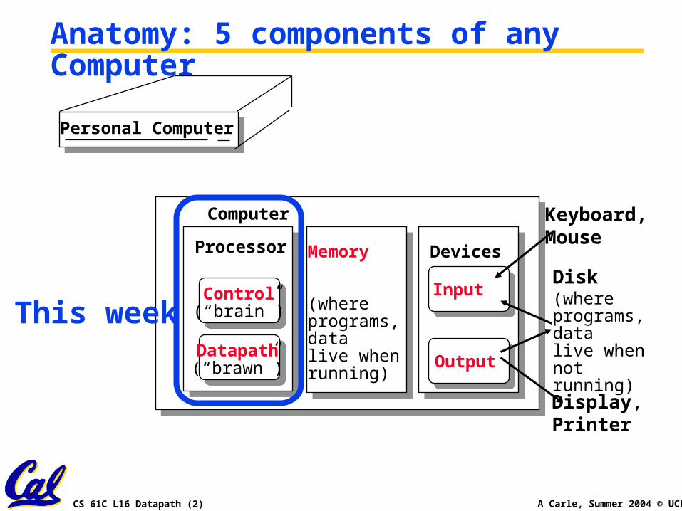
Anatomy: 5 components of any Computer
Personal Computer
Processor
Computer
Control(“brain”)
Datapath(“brawn”)
Memory
(where programs, data live whenrunning)
Devices
Input
Output
Keyboard, Mouse
Display, Printer
Disk (where programs, data live whennot running)
This week
CS 61C L16 Datapath (3) A Carle, Summer 2004 © UCB
Outline
• Design a processor: step-by-step
• Requirements of the Instruction Set
• Hardware components that match the instruction set requirements
CS 61C L16 Datapath (4) A Carle, Summer 2004 © UCB
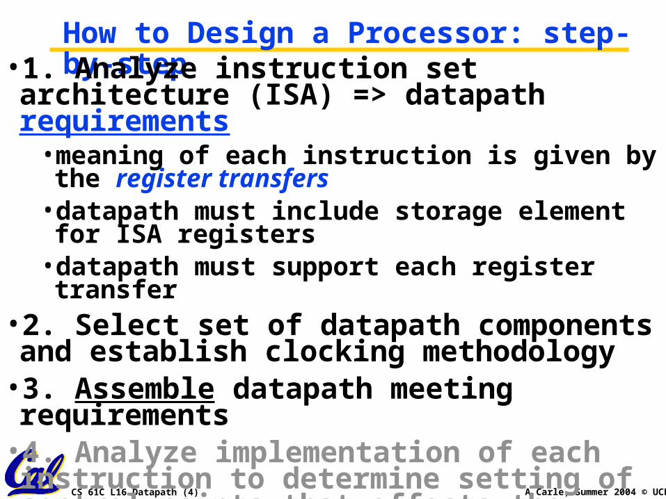
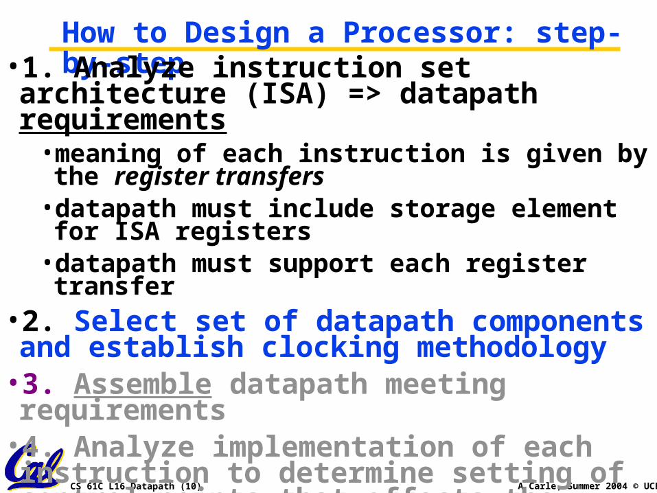
How to Design a Processor: step-by-step• 1. Analyze instruction set architecture (ISA)
=> datapath requirements• meaning of each instruction is given by the register transfers
• datapath must include storage element for ISA registers
• datapath must support each register transfer• 2. Select set of datapath components and establish clocking methodology
• 3. Assemble datapath meeting requirements• 4. Analyze implementation of each instruction to determine setting of control points that effects the register transfer.
• 5. Assemble the control logic
CS 61C L16 Datapath (5) A Carle, Summer 2004 © UCB
Step 1: The MIPS Instruction Formats• All MIPS instructions are 32 bits long. 3 formats:
• R-type
• I-type
• J-type
• The different fields are:• op: operation (“opcode”) of the instruction• rs, rt, rd: the source and destination register specifiers• shamt: shift amount• funct: selects the variant of the operation in the “op”
field• address / immediate: address offset or immediate value• target address: target address of jump instruction
op target address
02631
6 bits 26 bits
op rs rt rd shamt funct
061116212631
6 bits 6 bits5 bits5 bits5 bits5 bits
op rs rt address/immediate
016212631
6 bits 16 bits5 bits5 bits
CS 61C L16 Datapath (6) A Carle, Summer 2004 © UCB
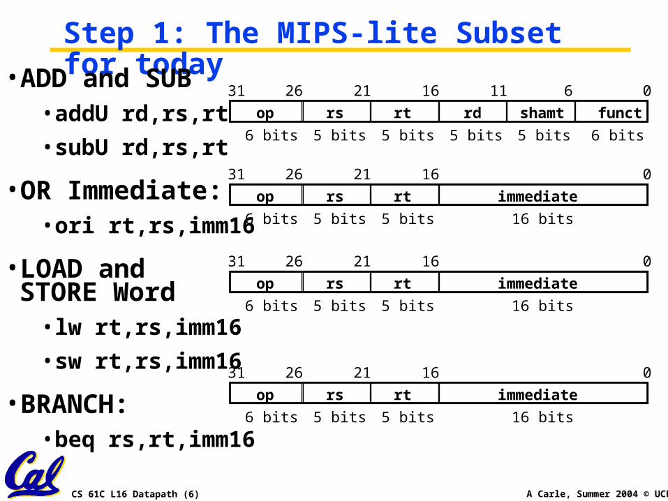
Step 1: The MIPS-lite Subset for today• ADD and SUB
•addU rd,rs,rt•subU rd,rs,rt
• OR Immediate:•ori rt,rs,imm16
• LOAD and STORE Word•lw rt,rs,imm16•sw rt,rs,imm16
• BRANCH:•beq rs,rt,imm16
op rs rt rd shamt funct
061116212631
6 bits 6 bits5 bits5 bits5 bits5 bits
op rs rt immediate
016212631
6 bits 16 bits5 bits5 bits
op rs rt immediate
016212631
6 bits 16 bits5 bits5 bits
op rs rt immediate
016212631
6 bits 16 bits5 bits5 bits
CS 61C L16 Datapath (7) A Carle, Summer 2004 © UCB
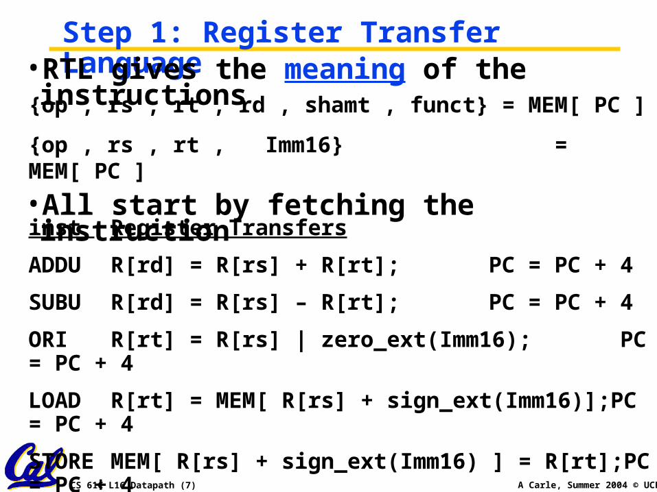
Step 1: Register Transfer Language• RTL gives the meaning of the instructions
• All start by fetching the instruction
{op , rs , rt , rd , shamt , funct} = MEM[ PC ]
{op , rs , rt , Imm16} = MEM[ PC ]
inst Register Transfers
ADDU R[rd] = R[rs] + R[rt]; PC = PC + 4
SUBU R[rd] = R[rs] – R[rt]; PC = PC + 4
ORI R[rt] = R[rs] | zero_ext(Imm16); PC = PC + 4
LOAD R[rt] = MEM[ R[rs] + sign_ext(Imm16)];PC = PC + 4
STORE MEM[ R[rs] + sign_ext(Imm16) ] = R[rt];PC = PC + 4
BEQ if ( R[rs] == R[rt] ) then PC = PC + 4 +sign_ext(Imm16)] << 2
else PC = PC + 4
CS 61C L16 Datapath (8) A Carle, Summer 2004 © UCB
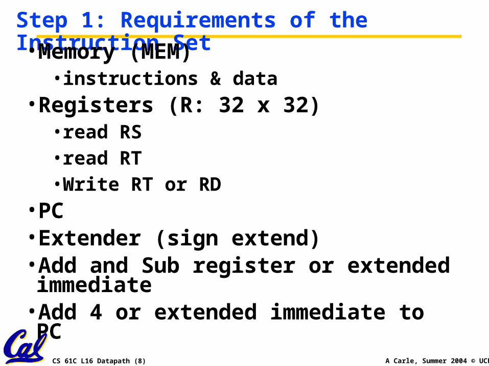
Step 1: Requirements of the Instruction Set• Memory (MEM)
• instructions & data• Registers (R: 32 x 32)
• read RS• read RT• Write RT or RD
• PC• Extender (sign extend)• Add and Sub register or extended immediate
• Add 4 or extended immediate to PC
CS 61C L16 Datapath (9) A Carle, Summer 2004 © UCB
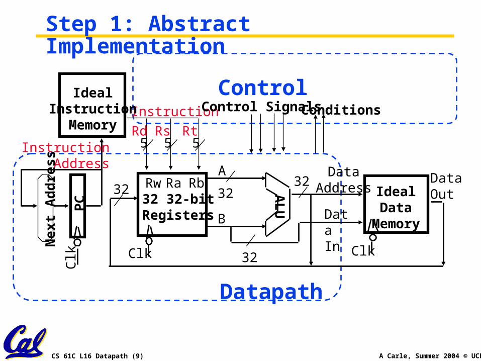
Step 1: Abstract Implementation
DataOut
Clk
5
Rw Ra Rb32 32-bitRegisters
Rd
AL
U
Clk
Data In
DataAddress Ideal
DataMemory
Instruction
InstructionAddress
IdealInstruction
Memory
Clk
PC
5Rs
5Rt
32
323232
A
B
Nex
t A
dd
ress
Control
Datapath
Control Signals Conditions
CS 61C L16 Datapath (10) A Carle, Summer 2004 © UCB
How to Design a Processor: step-by-step• 1. Analyze instruction set architecture (ISA)
=> datapath requirements• meaning of each instruction is given by the register transfers
• datapath must include storage element for ISA registers
• datapath must support each register transfer• 2. Select set of datapath components and establish clocking methodology
• 3. Assemble datapath meeting requirements• 4. Analyze implementation of each instruction to determine setting of control points that effects the register transfer.
• 5. Assemble the control logic (hard part!)
CS 61C L16 Datapath (11) A Carle, Summer 2004 © UCB
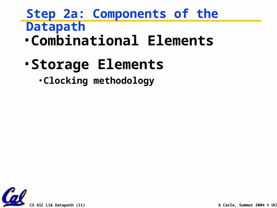
Step 2a: Components of the Datapath•Combinational Elements
•Storage Elements• Clocking methodology
CS 61C L16 Datapath (12) A Carle, Summer 2004 © UCB
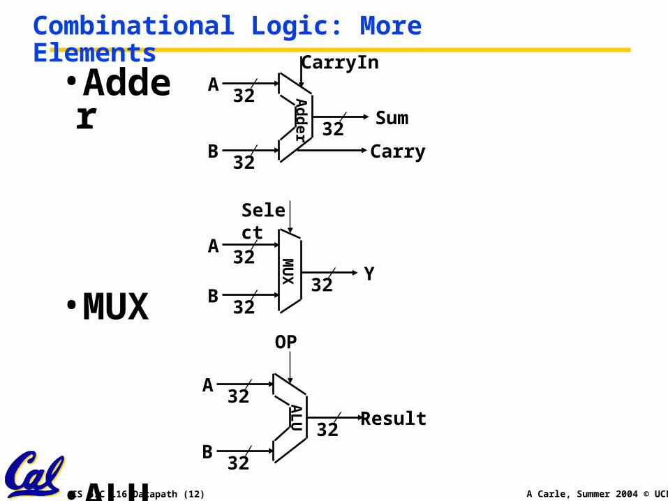
Combinational Logic: More Elements
•Adder
•MUX
•ALU
32
32
A
B32
Sum
Carry
32
32
A
B32
Result
OP
32A
B32
Y32
Select
Ad
der
MU
XA
LU
CarryIn
CS 61C L16 Datapath (13) A Carle, Summer 2004 © UCB
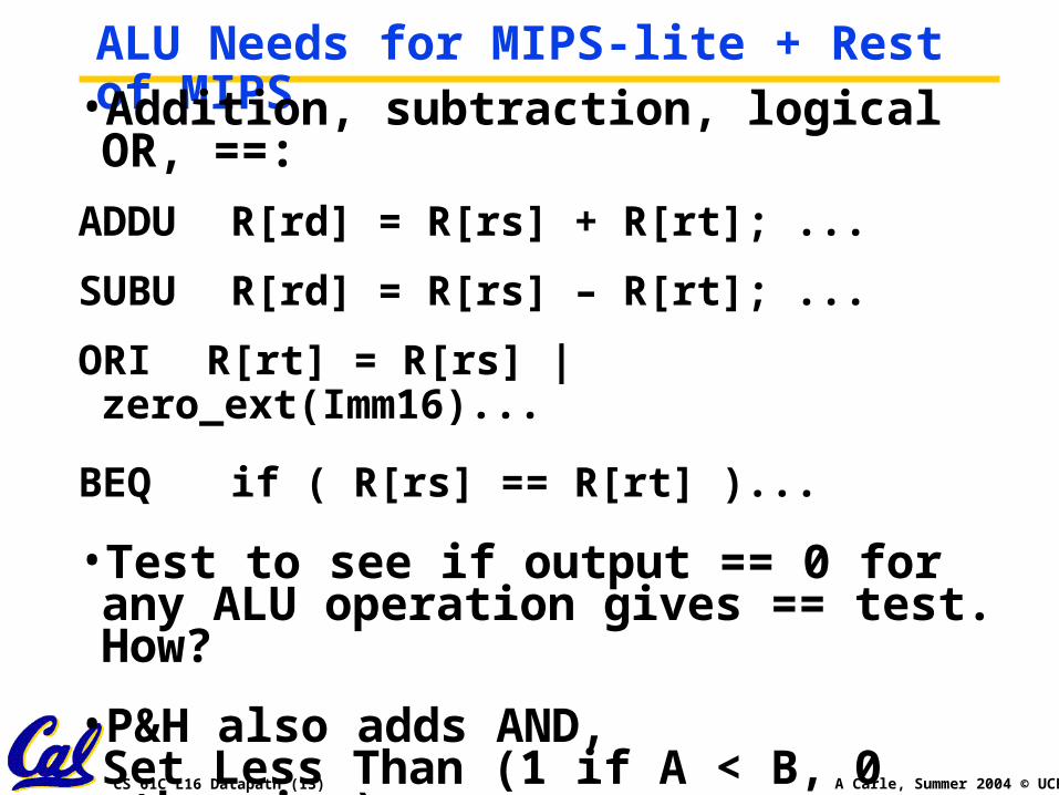
ALU Needs for MIPS-lite + Rest of MIPS• Addition, subtraction, logical OR, ==:
ADDU R[rd] = R[rs] + R[rt]; ...
SUBU R[rd] = R[rs] – R[rt]; ...
ORI R[rt] = R[rs] | zero_ext(Imm16)...
BEQ if ( R[rs] == R[rt] )...
• Test to see if output == 0 for any ALU operation gives == test. How?
• P&H also adds AND, Set Less Than (1 if A < B, 0 otherwise)
• ALU follows chap 5
CS 61C L16 Datapath (14) A Carle, Summer 2004 © UCB
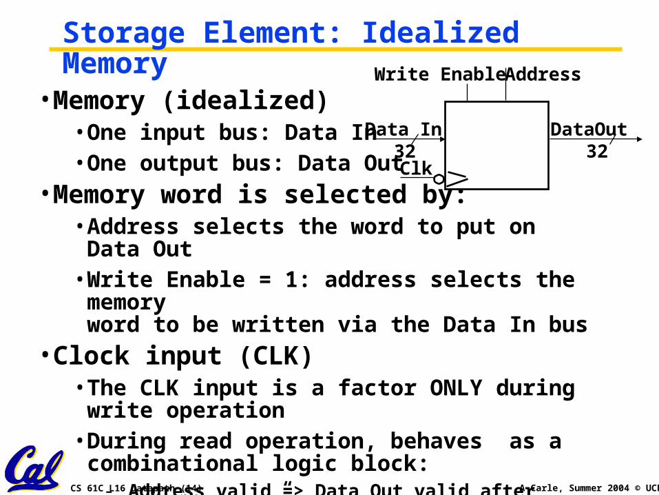
Storage Element: Idealized Memory
• Memory (idealized)• One input bus: Data In• One output bus: Data Out
• Memory word is selected by:• Address selects the word to put on Data Out• Write Enable = 1: address selects the memory
word to be written via the Data In bus• Clock input (CLK)
• The CLK input is a factor ONLY during write operation
• During read operation, behaves as a combinational logic block:
- Address valid => Data Out valid after “access time.”
Clk
Data In
Write Enable
32 32DataOut
Address
CS 61C L16 Datapath (15) A Carle, Summer 2004 © UCB
Clk
Data In
Write Enable
N N
Data Out
Storage Element: Register (Building Block)
• Similar to D Flip Flop except- N-bit input and output
- Write Enable input
• Write Enable:- negated (or deasserted) (0):
Data Out will not change
- asserted (1): Data Out will become Data In
CS 61C L16 Datapath (16) A Carle, Summer 2004 © UCB
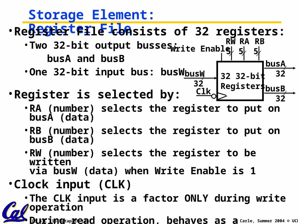
Storage Element: Register File• Register File consists of 32 registers:
• Two 32-bit output busses: busA and busB• One 32-bit input bus: busW
• Register is selected by:• RA (number) selects the register to put on busA (data)• RB (number) selects the register to put on busB (data)• RW (number) selects the register to be written
via busW (data) when Write Enable is 1• Clock input (CLK)
• The CLK input is a factor ONLY during write operation• During read operation, behaves as a combinational
logic block:- RA or RB valid => busA or busB valid after “access time.”
Clk
busW
Write Enable
3232
busA
32busB
5 5 5RWRA RB
32 32-bitRegisters
CS 61C L16 Datapath (17) A Carle, Summer 2004 © UCB
Administrivia• Turn in your HW 45 in class!
• Project 2 due Sunday• No extensions, No Excuses• Hope you’ve already started
• Midterm Re-Grades• Review the key that will be posted after lecture
- I decided to hold up to let you have maximum fun with the HW question
• If you feel you have a legit complaint, write up a description of the error and staple it to the front of your test
- Hand this in to Andy or a TA
CS 61C L16 Datapath (18) A Carle, Summer 2004 © UCB
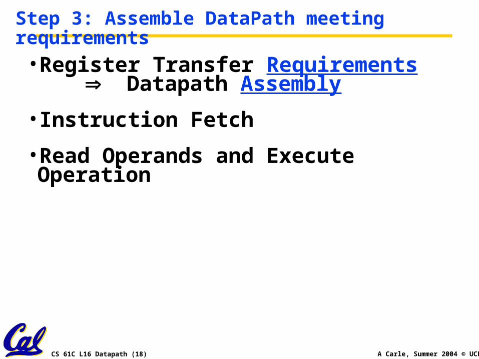
Step 3: Assemble DataPath meeting requirements
• Register Transfer Requirements Datapath Assembly
• Instruction Fetch
• Read Operands and Execute Operation
CS 61C L16 Datapath (19) A Carle, Summer 2004 © UCB
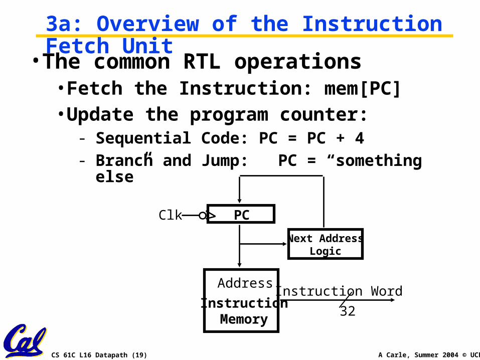
3a: Overview of the Instruction Fetch Unit
• The common RTL operations• Fetch the Instruction: mem[PC]• Update the program counter:
- Sequential Code: PC = PC + 4 - Branch and Jump: PC = “something else”
32
Instruction WordAddress
InstructionMemory
PCClk
Next AddressLogic
CS 61C L16 Datapath (20) A Carle, Summer 2004 © UCB
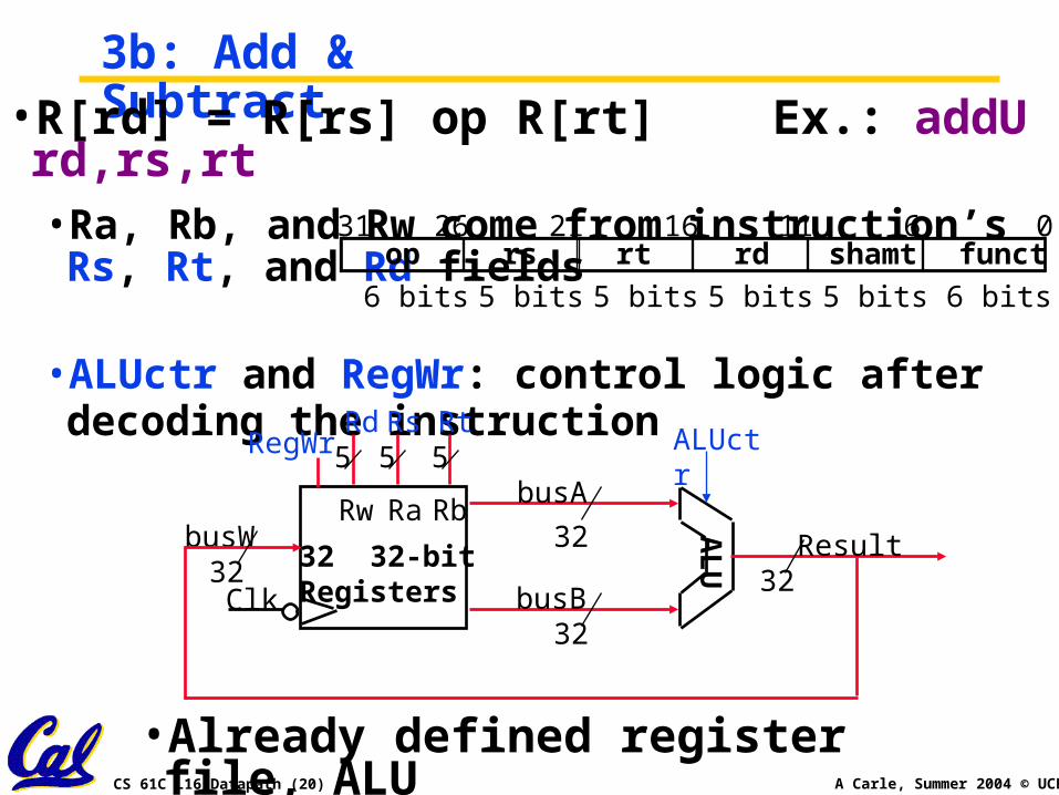
3b: Add & Subtract• R[rd] = R[rs] op R[rt] Ex.: addU rd,rs,rt
• Ra, Rb, and Rw come from instruction’s Rs, Rt, and Rd fields
• ALUctr and RegWr: control logic after decoding the instruction
32Result
ALUctr
Clk
busW
RegWr
3232
busA
32busB
5 5 5
Rw Ra Rb
32 32-bitRegisters
Rs RtRd
AL
U
op rs rt rd shamt funct061116212631
6 bits 6 bits5 bits5 bits5 bits5 bits
• Already defined register file, ALU
CS 61C L16 Datapath (21) A Carle, Summer 2004 © UCB
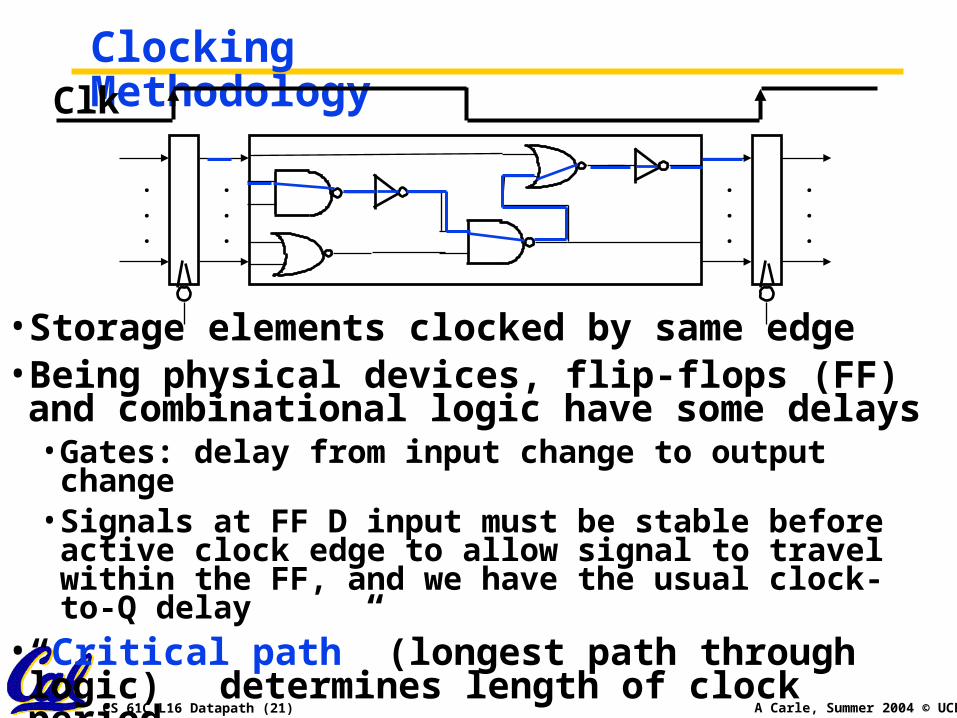
Clocking Methodology
• Storage elements clocked by same edge• Being physical devices, flip-flops (FF) and
combinational logic have some delays • Gates: delay from input change to output change • Signals at FF D input must be stable before active clock
edge to allow signal to travel within the FF, and we have the usual clock-to-Q delay
• “Critical path” (longest path through logic) determines length of clock period
Clk
.
.
.
.
.
.
.
.
.
.
.
.
CS 61C L16 Datapath (22) A Carle, Summer 2004 © UCB
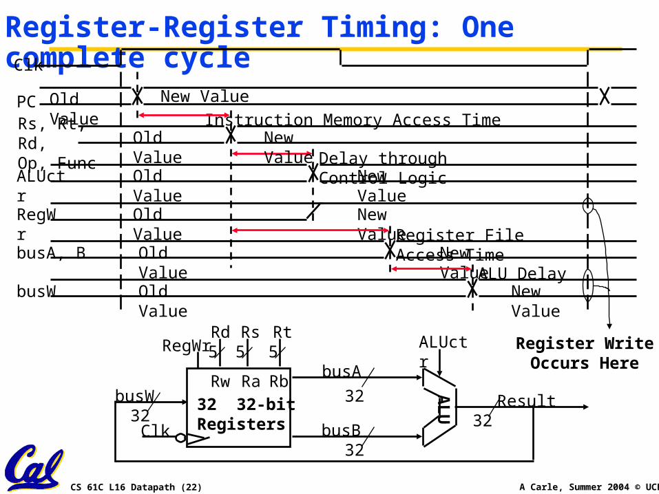
Register-Register Timing: One complete cycle
32Result
ALUctr
Clk
busW
RegWr
3232
busA
32busB
5 5 5
Rw Ra Rb
32 32-bitRegisters
Rs RtRd
AL
U
Clk
PCRs, Rt, Rd,Op, Func
ALUctr
Instruction Memory Access Time
Old Value New Value
RegWr Old Value New Value
Delay through Control Logic
busA, BRegister File Access TimeOld Value New Value
busWALU Delay
Old Value New Value
Old Value New Value
New ValueOld Value
Register WriteOccurs Here
CS 61C L16 Datapath (23) A Carle, Summer 2004 © UCB
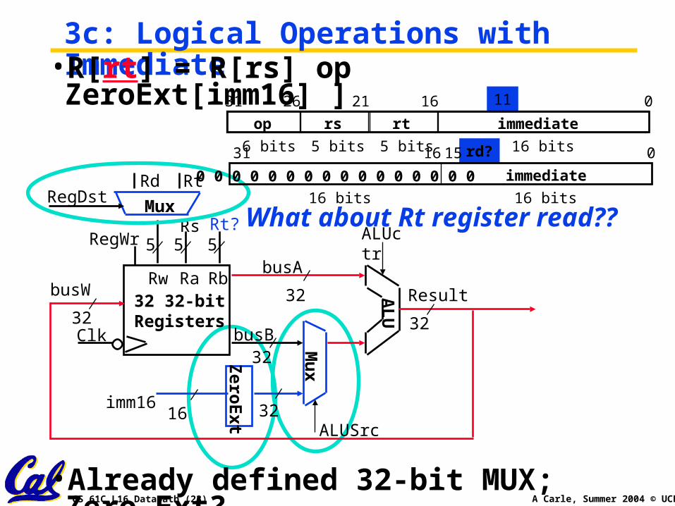
3c: Logical Operations with Immediate• R[rt] = R[rs] op ZeroExt[imm16] ]
32
Result
ALUctr
Clk
busW
RegWr
3232
busA
32busB
5 5 5
Rw Ra Rb32 32-bitRegisters
Rs
ZeroE
xt
Mu
x
RtRdRegDst
Mux
3216imm16
ALUSrc
AL
U
11
op rs rt immediate
016212631
6 bits 16 bits5 bits5 bits rd?
immediate
016 1531
16 bits16 bits
0 0 0 0 0 0 0 0 0 0 0 0 0 0 0 0
Rt?
• Already defined 32-bit MUX; Zero Ext?
What about Rt register read??
CS 61C L16 Datapath (24) A Carle, Summer 2004 © UCB
3d: Load Operations• R[rt] = Mem[R[rs] + SignExt[imm16]]Example: lw rt,rs,imm16
op rs rt immediate
016212631
6 bits 16 bits5 bits5 bits
32
ALUctr
Clk
busW
RegWr
32
32
busA
32
busB
5 5 5
Rw Ra Rb
32 32-bitRegisters
Rs
RtRd
RegDst
Exten
der
Mu
x
Mux
3216
imm16
ALUSrc
ExtOp
Clk
Data InWrEn
32
Adr
DataMemory
32
AL
U
MemWr Mu
x
W_Src
??
Rt
CS 61C L16 Datapath (25) A Carle, Summer 2004 © UCB
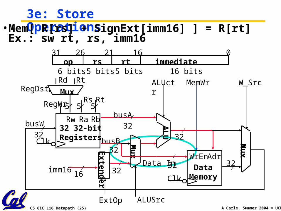
3e: Store Operations• Mem[ R[rs] + SignExt[imm16] ] = R[rt]
Ex.: sw rt, rs, imm16
op rs rt immediate016212631
6 bits 16 bits5 bits5 bits
32
ALUctr
Clk
busW
RegWr
3232
busA
32busB
55 5
Rw Ra Rb32 32-bitRegisters
Rs
Rt
Rt
RdRegDst
Exten
der
Mu
x
Mux
3216imm16
ALUSrcExtOp
Clk
Data InWrEn
32Adr
DataMemory
MemWr
AL
U
32
Mu
x
W_Src
CS 61C L16 Datapath (26) A Carle, Summer 2004 © UCB
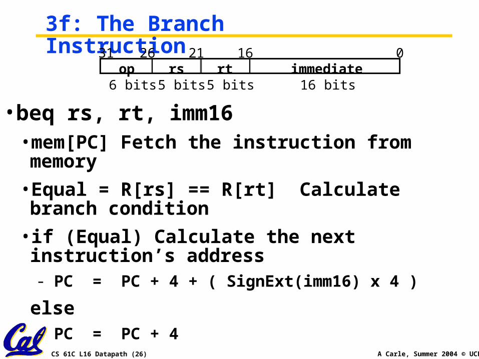
3f: The Branch Instruction
•beq rs, rt, imm16• mem[PC] Fetch the instruction from memory
• Equal = R[rs] == R[rt] Calculate branch condition
• if (Equal) Calculate the next instruction’s address- PC = PC + 4 + ( SignExt(imm16) x 4 )
else- PC = PC + 4
op rs rt immediate016212631
6 bits 16 bits5 bits5 bits
CS 61C L16 Datapath (27) A Carle, Summer 2004 © UCB
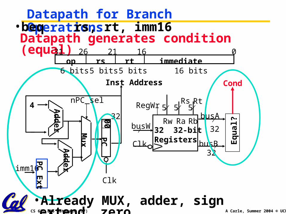
Datapath for Branch Operations• beq rs, rt, imm16
Datapath generates condition (equal)
op rs rt immediate016212631
6 bits 16 bits5 bits5 bits
32
imm16
PC
Clk
00
Ad
der
Mu
x
Ad
der
4nPC_sel
Clk
busW
RegWr
32
busA
32busB
5 5 5
Rw Ra Rb32 32-bitRegisters
Rs Rt
Eq
ual
?
Cond
PC
Ext
Inst Address
• Already MUX, adder, sign extend, zero
CS 61C L16 Datapath (28) A Carle, Summer 2004 © UCB
Putting it All Together:A Single Cycle Datapath
imm
16
32
ALUctr
Clk
busW
RegWr
3232
busA
32busB
55 5
Rw Ra Rb32 32-bitRegisters
Rs
Rt
Rt
RdRegDst
Exten
der
Mu
x
3216imm16
ALUSrcExtOp
Mu
x
MemtoReg
Clk
Data InWrEn32 Adr
DataMemory
MemWrA
LU
Equal
Instruction<31:0>
0
1
0
1
01
<21:25>
<16:20>
<11:15>
<0:15>
Imm16RdRtRs
=
Ad
der
Ad
der
PC
Clk
00Mu
x
4
nPC_sel
PC
Ext
Adr
InstMemory
CS 61C L16 Datapath (29) A Carle, Summer 2004 © UCB
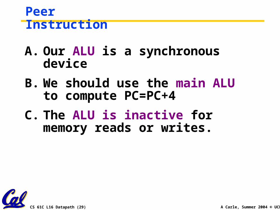
Peer Instruction
A. Our ALU is a synchronous device
B. We should use the main ALU to compute PC=PC+4
C. The ALU is inactive for memory reads or writes.
CS 61C L16 Datapath (30) A Carle, Summer 2004 © UCB
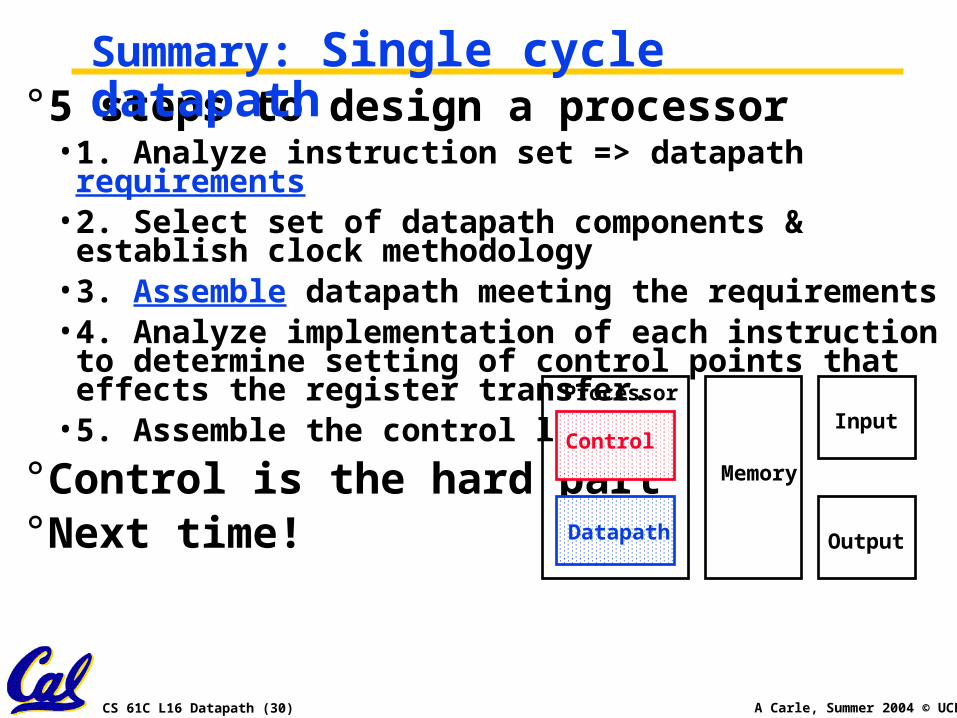
°5 steps to design a processor• 1. Analyze instruction set => datapath requirements• 2. Select set of datapath components & establish clock
methodology• 3. Assemble datapath meeting the requirements• 4. Analyze implementation of each instruction to
determine setting of control points that effects the register transfer.
• 5. Assemble the control logic
°Control is the hard part°Next time!
Summary: Single cycle datapath
Control
Datapath
Memory
ProcessorInput
Output