CS 35101 Computer Architecture
95
CS 35101 Computer Architecture Section 600 Dr. Angela Guercio Fall 2010
Transcript of CS 35101 Computer Architecture
CS 35101 Computer Architecture
Section 600
Dr. Angela GuercioFall 2010
Gates
A digital circuit is one in which only two logical values are present.
• Typically, a signal between 0 and 1 volt represents one value (e.g. binary 0) and a signal between 2 and 5 volts represents the other value (e.g. binary 1).
Tiny electronic devices, called gates, can compute various functions of these two-valued signals.
• Gates form the basis on which all digital computers are built.
Gates
A transistor can be made to operate as a very fast binary switch. The next slide shows a bipolar transistor (the
circle) embedded in a simple circuit. The transistor has three connections to the outside:
the collector the base the emitter
• When the Vin is below a certain critical value, the transistor turns off and acts like an infinite resistance. This causes Vout to to take on a value close to Vcc.
Gates
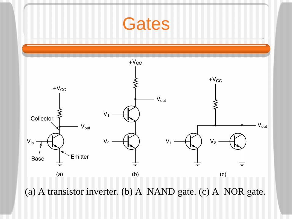
• When Vin exceeds the critical value, the transistor switches on and acts like a wire, causing Vout to be pulled down to 0 volts.
• This circuit is an inverter, converting a logical 0 to a logical 1, and vice versa. The resistor is needed to limit the amount of current drawn by the transistor.
• In the next figure, if both inputs are high, the output will be low. If either output is low, the output will be high.
• In the third figure, the transistors are wired in parallel rather than series. If either input is high, the transistor will turn on and pull the output down.
Gates
(a) A transistor inverter. (b) A NAND gate. (c) A NOR gate.
Gates
These three circuits form the three simplest gates:
• NOT gates• NAND gates• NOR gates
NOT gates are also called inverters. If we now adopt the convention that “high” is a
logical 1, and that “low” (ground) is a logical 0, we can express the output values as a function of the input values.
Gates
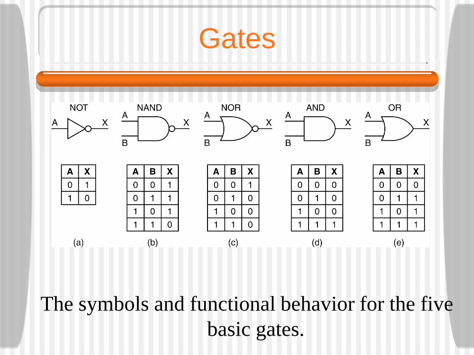
The symbols and functional behavior for the five basic gates.
Gates
If the output of the NAND gate is fed into an inverter circuit, we get another circuit with precisely the inverse of the NAND gate - an AND gate. The NOR gate can be connected to an inverter
to yield an OR gate. The small circles used as part of the symbols for the inverter etc. are called inversion bubbles. The five gates described are the principal
building blocks of the digital logic level.
Gates
• NAND and NOR gates require two transistors each, while the AND and OR gates require three transistors each. Therefore, many computers are based on NAND and NOR gates rather than AND and OR.
• The two major technologies for constructing gates are bipolar and MOS (Metal Oxide Semiconductor). The major bipolar types are TTL(Transistor-Transistor Logic) and ECL (Emitter-Coupled Logic). MOS gates are slower than TTL and ECL but require less power and space. Most modern CPUs and memories use CMOS technology which runs on +3.3 volts.
Boolean Algebra
Boolean Algebra can be used to describe the circuits that can be built by combining gates. A Boolean function has one or more input
variables and yields a result that depends only those variables.
• Define a function f such that f(A) is 1 if A is 0 and f(A) is 0 if A is 1. This function is the NOT function.
Since a Boolean function of n variables has only 2n possible combinations of inputs, the function can be completely described by giving a truth table with 2n rows of inputs/output.
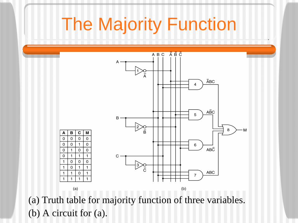
The Majority Function
(a) Truth table for majority function of three variables.(b) A circuit for (a).
Boolean Algebra
Although any Boolean function can be specified by giving its truth table, this notation becomes cumbersome as the number of variables increases. Another notation is based on the fact that any
Boolean function can be specified by telling which combinations of input variables give an output value of 1.
• An apostrophe after an input variable means that its value is inverted. The absence of an apostrophe means that it is not inverted.
Boolean Algebra
Implied multiplication (or a dot) means the Boolean AND function and + means the Boolean OR function.
• Example: AB’C takes the value 1 only when A = 1, B = 0 , and C = 1.
• The previous truth table can be written as M = A’BC + AB’C + ABC’ + ABC as a compact way of giving the truth table.
• A function of n variables can be described by giving a “sum” of at most 2n n-variable “product” terms.
Boolean Algebra
The formulation of a Boolean function as a sum of up to 2n products leads directly to a possible implementation as shown.
• We can implement a circuit for any Boolean function by: Writing down the truth table for the function Providing inverters to generate the complement of each
input Drawing an AND gate for each term with a 1 in the result
column Wiring the AND gates to the appropriate inputs Feeding the output of all the AND gates into an OR gate
Boolean Algebra
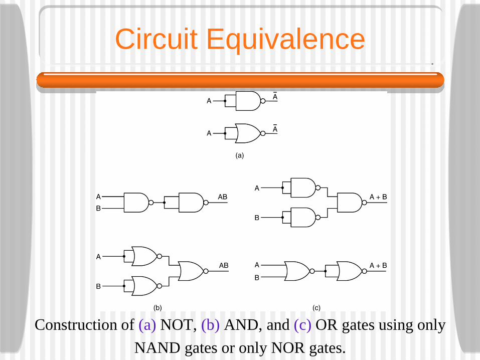
It is often convenient to implement circuits using only a single gate type. It is straightforward to convert circuits
generated by the previous algorithm to pure NAND or pure NOR form - all we need is a way to implement NOT, AND, and OR using a single gate type. Both NAND and NOR gates are said to be
complete, because any Boolean function can be computed using either of them.
Boolean Algebra
No other gate has this property. Follow the previous algorithm then replace the
multi-input gates with equivalent circuits using two-input gates. Replace the NOT, AND, and OR gates with the circuits of the following slide.
Circuit Equivalence
Construction of (a) NOT, (b) AND, and (c) OR gates using only NAND gates or only NOR gates.
Circuit Equivalence
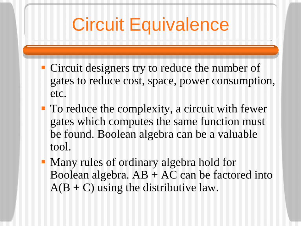
Circuit designers try to reduce the number of gates to reduce cost, space, power consumption, etc. To reduce the complexity, a circuit with fewer
gates which computes the same function must be found. Boolean algebra can be a valuable tool. Many rules of ordinary algebra hold for
Boolean algebra. AB + AC can be factored into A(B + C) using the distributive law.
Circuit Equivalence
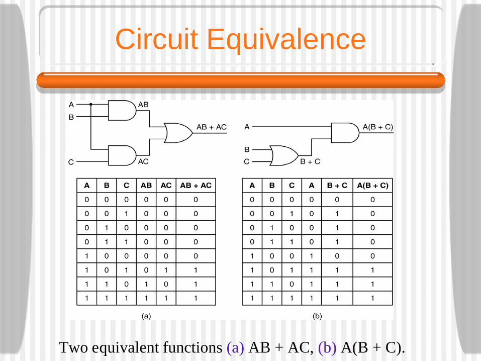
Two equivalent functions (a) AB + AC, (b) A(B + C).
Circuit Equivalence
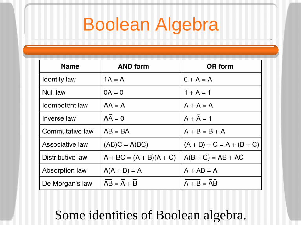
In general, a designer starts with a Boolean function and then applies the laws of Boolean algebra to find a simpler but equivalent one. From the final function, a circuit can be constructed. Some of the major identifies from Boolean
algebra are shown in the following slide. Note that each law has two forms that are duals of each other. By interchanging AND and OR and also 0 and 1, either form can be produced from the other one.
Boolean Algebra
Some identities of Boolean algebra.
DeMorgan’s Law
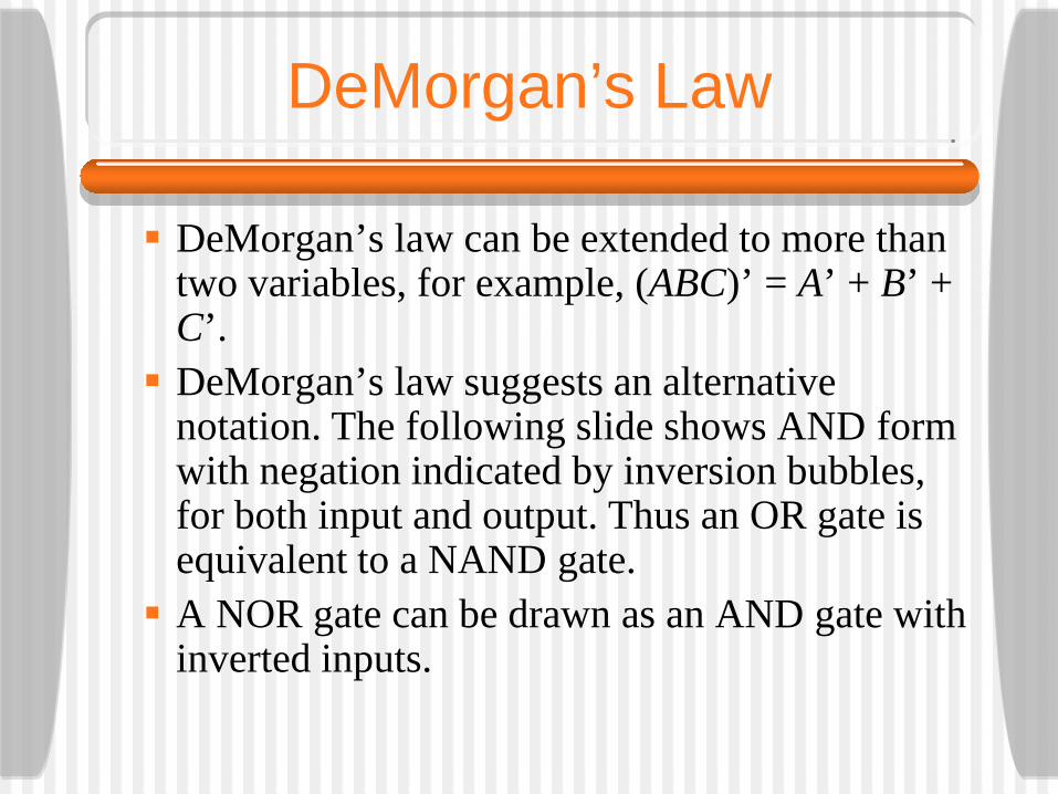
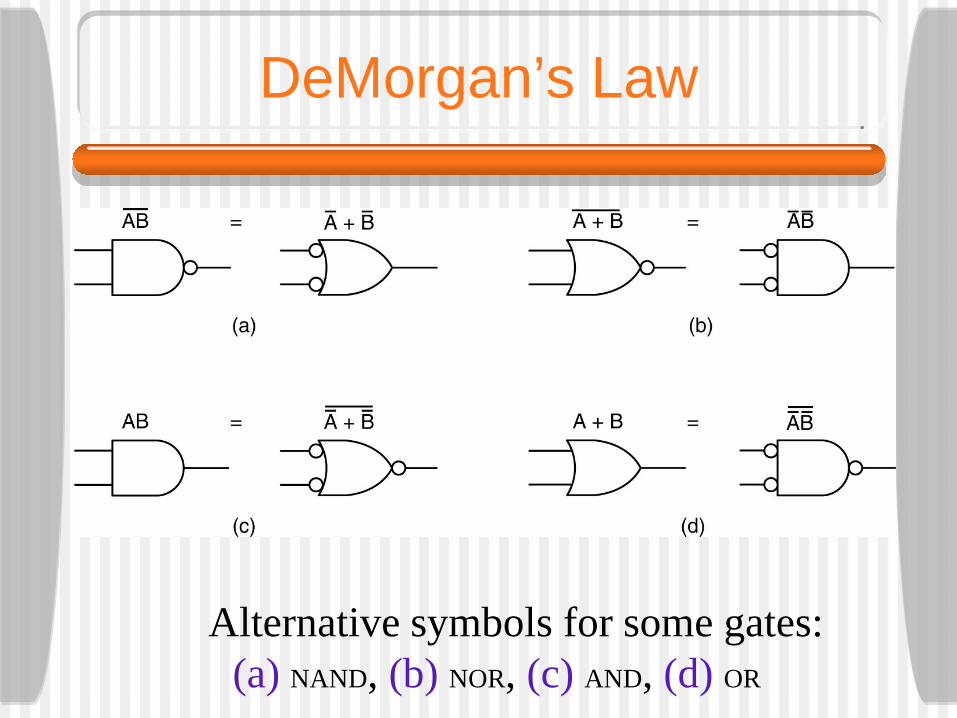
DeMorgan’s law can be extended to more than two variables, for example, (ABC)’ = A’ + B’ + C’. DeMorgan’s law suggests an alternative
notation. The following slide shows AND form with negation indicated by inversion bubbles, for both input and output. Thus an OR gate is equivalent to a NAND gate. A NOR gate can be drawn as an AND gate with
inverted inputs.
DeMorgan’s Law
Alternative symbols for some gates:(a) NAND, (b) NOR, (c) AND, (d) OR
DeMorgan’s Law
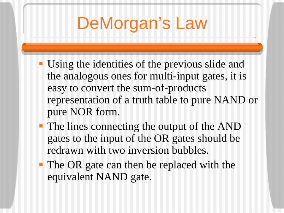
Using the identities of the previous slide and the analogous ones for multi-input gates, it is easy to convert the sum-of-products representation of a truth table to pure NAND or pure NOR form. The lines connecting the output of the AND
gates to the input of the OR gates should be redrawn with two inversion bubbles. The OR gate can then be replaced with the
equivalent NAND gate.
Boolean Algebra
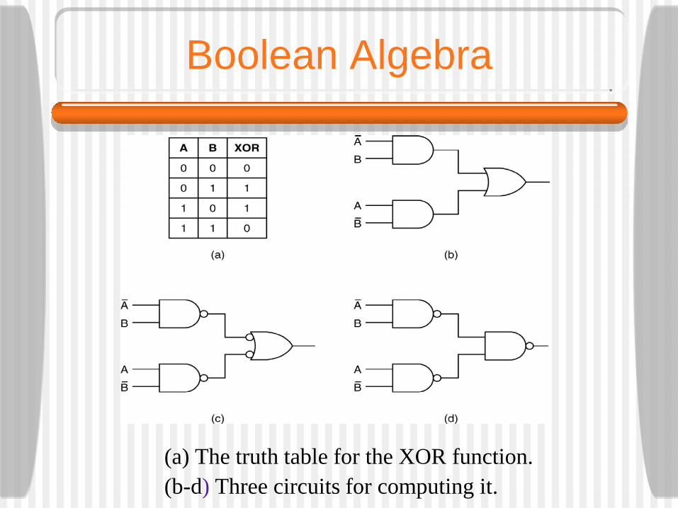
(a) The truth table for the XOR function.(b-d) Three circuits for computing it.
Circuit Equivalence
The same physical gate can compute different functions, depending on the conventions used. The following slide shows the output of a
certain gate F, for different input combinations.• Both inputs and outputs are shown in volts.• If we adopt the convention that 0 volts is logical 0
and 3.3 or 5 volts is logical 1, called positive logic, we have one result. If, however, we adopt negative logic, which has 0 volts as logical 1 and 3.3 or 5 volts as logical 0, we get another function, the OR function. Usually, we will assume positive logic.
Positive and Negative Logic
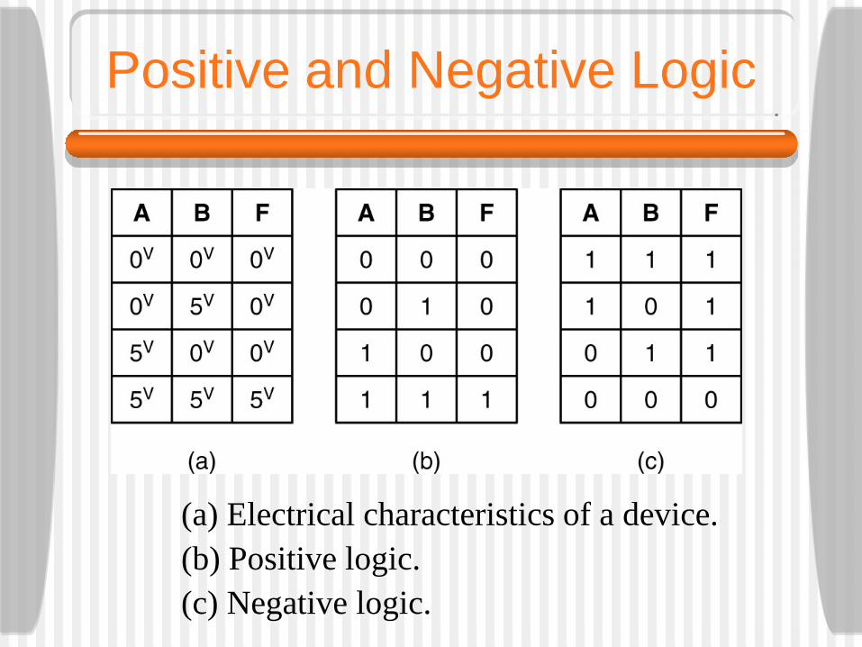
(a) Electrical characteristics of a device.(b) Positive logic.(c) Negative logic.
Integrated Circuits
Gates are not manufactured or sold individually, but rather in units called Integrated Circuits, often called ICs or chips. An IC is a square piece of silicon on which
some gates have been deposited. Small ICs are usually mounted in rectangular plastic or ceramic packages measuring 5 to 15 mm wide and 20 to 50 mm long.
• Along the long edges are two parallel rows of pins that can be inserted into sockets or soldered to printed circuit boards.
Integrated Circuits
The packages with two rows of pins outside and ICs inside are technically known as Dual Inline Packages or DIPs, but everyone calls them chips. The most common packages have 14, 16, 18,
20, 22, 24, 28, 40, 64, or 68 pins. For large chips, square packages with pins on all four sides are often used. Chips can be divided into rough classes based
on the number of gates they contain:
Integrated Circuits
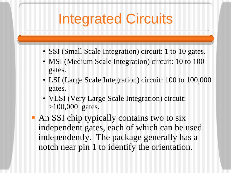
• SSI (Small Scale Integration) circuit: 1 to 10 gates.• MSI (Medium Scale Integration) circuit: 10 to 100
gates.• LSI (Large Scale Integration) circuit: 100 to 100,000
gates.• VLSI (Very Large Scale Integration) circuit:
>100,000 gates. An SSI chip typically contains two to six
independent gates, each of which can be used independently. The package generally has a notch near pin 1 to identify the orientation.
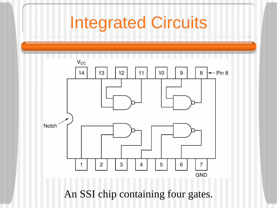
Integrated Circuits
An SSI chip containing four gates.
Integrated Circuits
Many chips like this are available for a few cents each. In the 1970s, computers were constructed out of a large number of these chips. Today an entire CPU and cache memory are etched onto a single chip. We can consider all gates to be ideal so that
output appears as soon as input is applied. In reality chips have a finite gate delay which includes signal propagation time and switching time. Typical delays are 1 to 10 nsec.

Combinatorial Circuits
Many applications of digital logic require a circuit with multiple inputs and multiple outputs in which the outputs are uniquely determined by the current inputs. Such a circuit is called a combinatorial circuit. Not all circuits have this property (e.g. memory
elements). A circuit implementing a truth table is a typical example of a combinatorial circuit.
Multiplexers
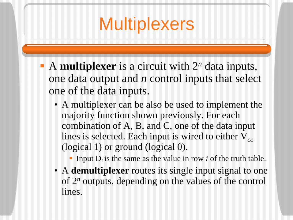
A multiplexer is a circuit with 2n data inputs, one data output and n control inputs that select one of the data inputs.
• A multiplexer can be also be used to implement the majority function shown previously. For each combination of A, B, and C, one of the data input lines is selected. Each input is wired to either Vcc(logical 1) or ground (logical 0). Input Di is the same as the value in row i of the truth table.
• A demultiplexer routes its single input signal to one of 2n outputs, depending on the values of the control lines.
Multiplexers
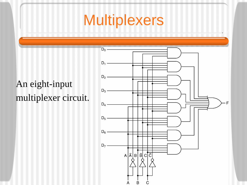
An eight-input multiplexer circuit.
Multiplexers
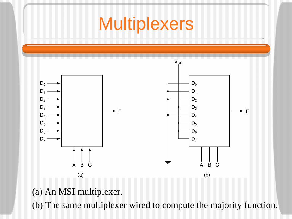
(a) An MSI multiplexer.(b) The same multiplexer wired to compute the majority function.
Decoders
• A decoder takes an n-bit number as input and uses it to select (i.e. set to 1) exactly one of the 2n output lines.
• A decoder can be used, for example, to select 1 of 8 memory chips given the high-order 3 bits of the address if the chips are organized so that chip 0 has addresses 0 to 1 MB, chip 1 has addresses 1 MB to 2 MB, and so on.
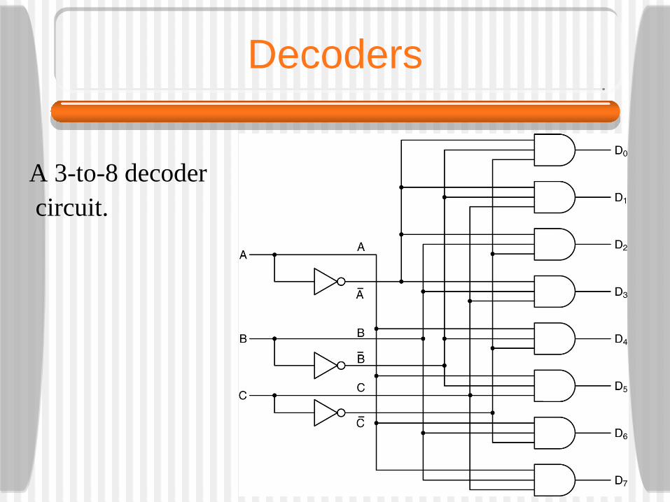
Decoders
A 3-to-8 decodercircuit.
Comparators
A comparator compares two input words. The following slide shows a simple comparator
which takes two inputs, A, and B, each of length 4 bits, and produces 1 if they are equal and a 0 if they are not equal.
• The circuit is based on the XOR gate (EXCLUSIVE OR) gate, which puts out a 0 if its inputs are equal and a 1 if they are unequal.
• If the two words are equal, all four of the XOR gates must output 0. The results are then combined with a NOR gate.
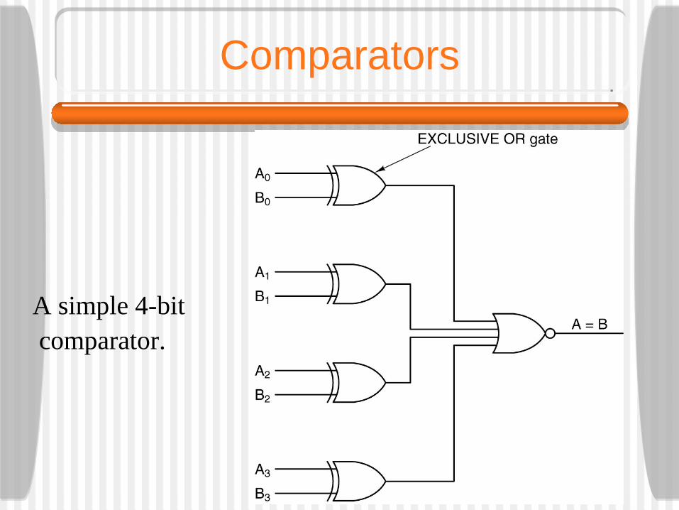
Comparators
A simple 4-bitcomparator.

Programmable Logic Arrays
Arbitrary functions (truth tables) can be constructed by computing product terms with AND gates and then ORing the products together. A very general chip for forming the sums of
products is the Programmable Logic Array or PLA. An example is shown on the following slide.
• The user programs this array by burning out selected fuses (there are 1200 total fuses). The fuses burned determine which signals go to each AND gate.
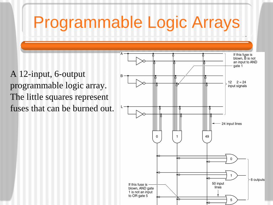
Programmable Logic Arrays
A 12-input, 6-outputprogrammable logic array.The little squares representfuses that can be burned out.
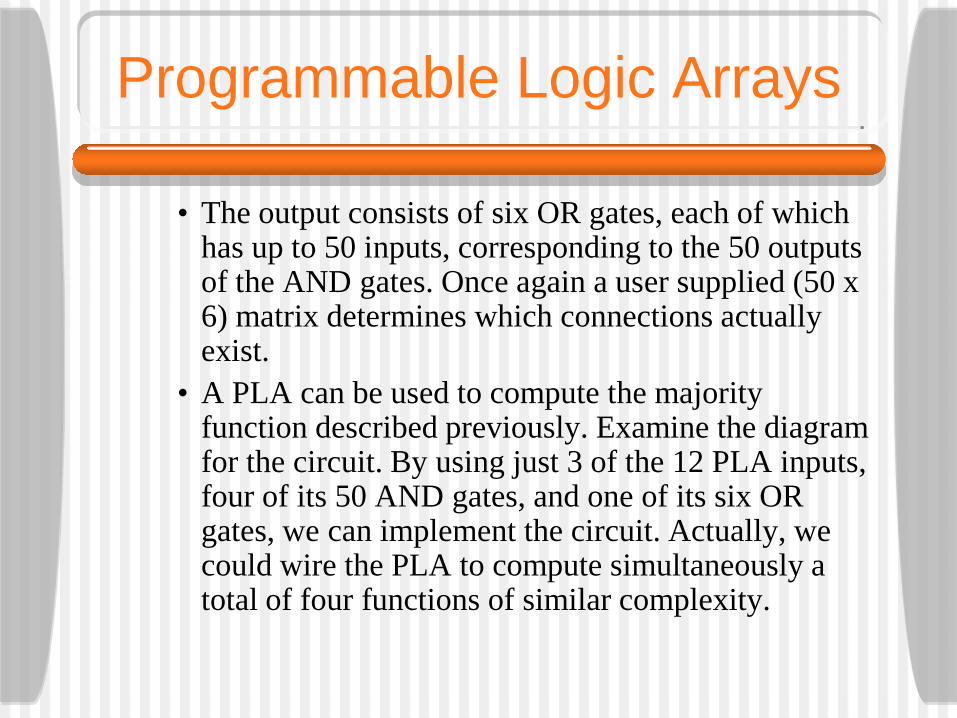
Programmable Logic Arrays
• The output consists of six OR gates, each of which has up to 50 inputs, corresponding to the 50 outputs of the AND gates. Once again a user supplied (50 x 6) matrix determines which connections actually exist.
• A PLA can be used to compute the majority function described previously. Examine the diagram for the circuit. By using just 3 of the 12 PLA inputs, four of its 50 AND gates, and one of its six OR gates, we can implement the circuit. Actually, we could wire the PLA to compute simultaneously a total of four functions of similar complexity.
Programmable Logic Arrays
Field-programmable PLAs (shipped from the factories with all fuses intact and then programmed by the user) are still in use, but for many applications custom-made PLAs are preferable.
• These are designed by the (large-volume) customer and fabricated by the manufacturer to the customer’s specifications. Such PLAs are cheaper than field-programmable ones.
We have seen three ways to compute the majority function.
Arithmetic Circuits
• We now move from general-purpose MSI circuits to MSI combinatorial circuits used for doing arithmetic. The first arithmetic MSI circuit we will
examine is an eight-input, eight-output shifter. Eight bits of input are presented on lines D0, …
, D7. The output, which is just the input shifted 1 bit is available on lines S0, … , S7. The control line, C, determines the direction of the shift, 0 for left and 1 for right.
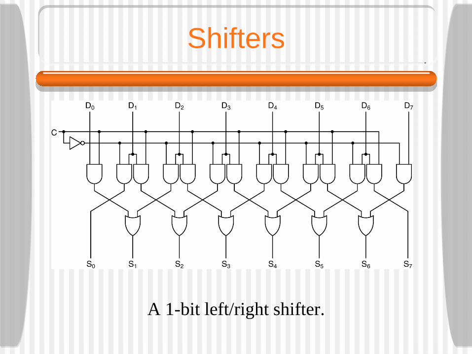
Shifters
A 1-bit left/right shifter.
Adders
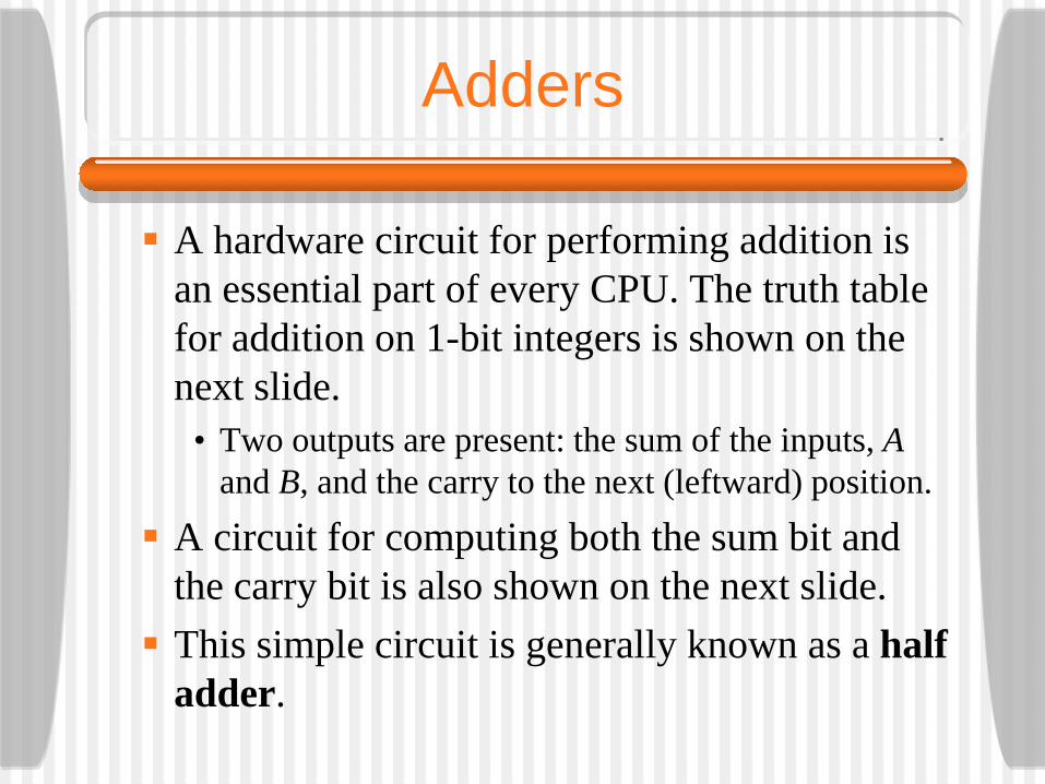
A hardware circuit for performing addition is an essential part of every CPU. The truth table for addition on 1-bit integers is shown on the next slide.
• Two outputs are present: the sum of the inputs, Aand B, and the carry to the next (leftward) position.
A circuit for computing both the sum bit and the carry bit is also shown on the next slide. This simple circuit is generally known as a half
adder.

Adders
(a) A truth table for 1-bit addition.(b) A circuit for a half adder.
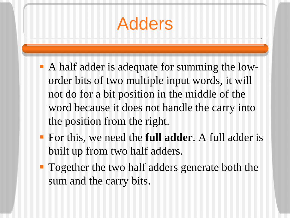
Adders
A half adder is adequate for summing the low-order bits of two multiple input words, it will not do for a bit position in the middle of the word because it does not handle the carry into the position from the right. For this, we need the full adder. A full adder is
built up from two half adders. Together the two half adders generate both the
sum and the carry bits.
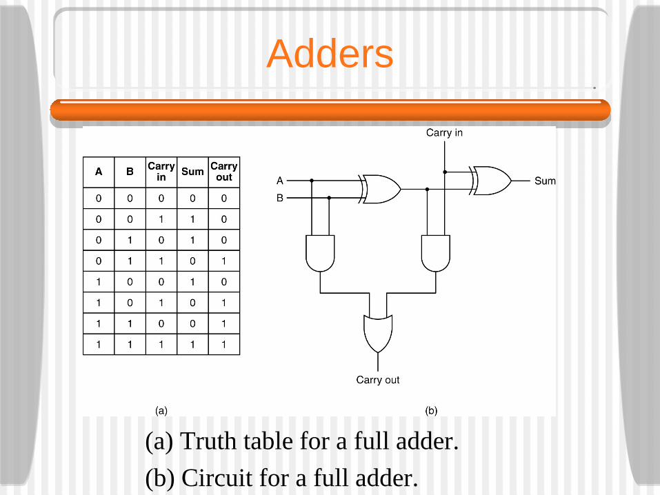
Adders
(a) Truth table for a full adder.(b) Circuit for a full adder.
Adders
To build an adder for, say, two 16-bit words one just replicates the circuit 16 times. The carry out of a bit is used as the carry into its left neighbor. The carry into the rightmost bit is wired to 0. This type of adder is called a ripple carry
adder because in the worst case, adding 1 to 111 … 111 (binary), the addition cannot complete until the carry has rippled all the way from the rightmost bit to the leftmost bit. Adders without this delay are preferred.
Adders
Consider giving the adder two upper halves operating in parallel by duplicating the upper half’s hardware. Now instead of a single 32-bit adder, we have three 16-bit adders. Call the upper halves U0 and U1. A 0 is fed
into U0 as a carry and a 1 is fed into U1 as a carry. Now both start at the same time as the lower half starts, but only one will be correct. Select the correct one based on the lower half’s output. This is called a carry select adder. And the replication can be repeated.
Arithmetic Logic Units
Most computers contain a single circuit for performing the AND, OR, and sum of two machine words. Typically, such a circuit for n-bit words is built up of n identical circuits for the individual bit positions and is called an Arithmetic Logic Unit or ALU. An ALU capable of computing A AND B, A
OR B, B’, or A + B, depending on the function select lines F0 and F1 is shown on the following slide.
Arithmetic Logic Units
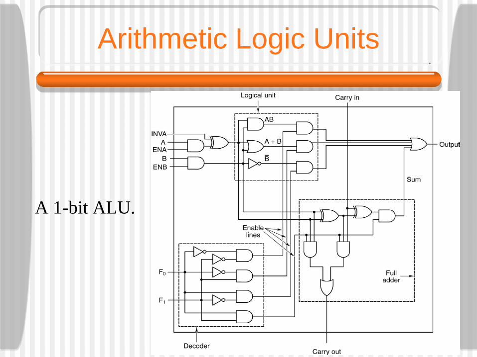
A 1-bit ALU.
Arithmetic Logic Units
The lower left-hand corner of the ALU contains a 2-bit decoder to generate enable signals for the four operations, based on the control signals F0 and F1. Exactly one of the four enable lines is selected. A or B can be forced to 0 by negating ENA or
ENB, respectively. It is also possible to get A’, by setting INVA. Under normal conditions, ENA and ENB are both 1 to enable both inputs and INVA is 0. We will later see uses for INVA, ENA, and ENB.
Arithmetic Logic Units
The lower right-hand corner of the ALU contains a full adder for computing the sum of A and B, including handling the carries, because it is likely that several of these circuits will eventually be wired together to perform full-word operations. Circuits like the one shown are actually
available and are known as bit slices. They allow the computer designer to build an ALU of any desired width.

Arithmetic Logic Units
Eight 1-bit ALU slices connected to make an 8-bit ALU. The enables and invert signals are not shown for simplicity.
Clocks
In many digital circuits the order in which events happen is critical. To allow designers to achieve the required
timing relations, many digital circuits use clocks to provide synchronization. A clock is a circuit that emits a series of pulses
with a precise pulse width and precise interval between consecutive pulses.
• The time interval between the corresponding edges of two consecutive pulses is known as the clock cycle time.
Clocks
Pulse frequencies are commonly between 1 and 500 MHz, corresponding to clock cycles of 1000 nsec to 2 nsec.
• To achieve high accuracy, the clock frequency is usually controlled by a crystal oscillator.
In a computer, many events may occur during a single clock cycle. If these events must occur in a certain order, the clock cycle must be divided into subcycles. A secondary clock signal phase-shifted from the primary may be generated with a delay circuit.
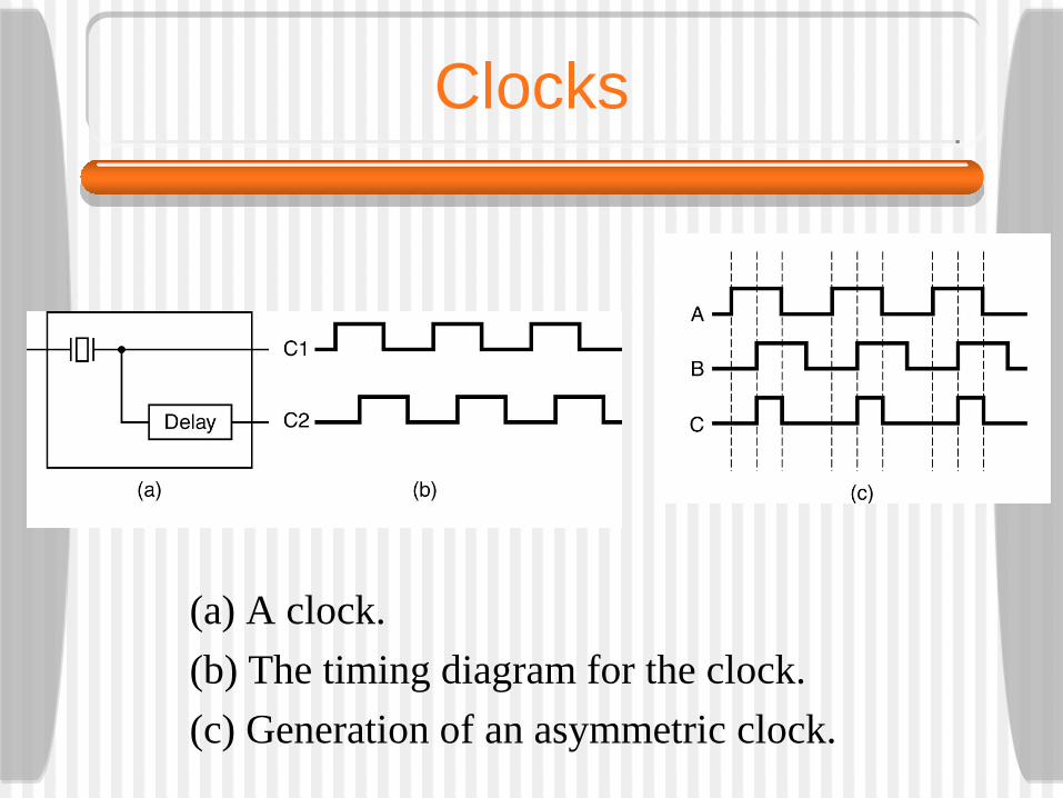
Clocks
(a) A clock.(b) The timing diagram for the clock.(c) Generation of an asymmetric clock.
Clocks
The four time references are:• Rising edge of C1• Falling edge of C1• Rising edge of C2• Falling edge of C2
By tying different events to the various edges, the required sequencing can be achieved. If more than four time references are needed, more secondary lines can be tapped from the primary, with different delays.
Memory
Memory is an essential component of every computer. We will now see the basic components of a memory system starting at the gate level. To create a 1-bit memory, we need a circuit that
remembers previous input values. Such a circuit can be constructed from two NOR gates. Analogous circuits can be built from NAND gates.
Latches
The circuit on the next slide is called an SR latch.
• It has two inputs, S, for Setting the latch and R, for Resetting it.
• It also has two outputs, Q and Q’, which are complementary.
• Unlike a combinatorial circuit, the outputs of the latch are not uniquely determined by the current inputs.
• Assume that both S and R are 0. Assume that Q = 0. Because Q is fed back into the upper NOR gate, both of its inputs are 0, so its output is 1.
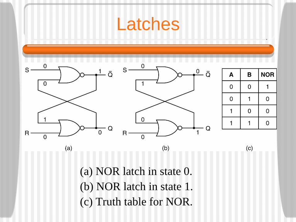
Latches
(a) NOR latch in state 0.(b) NOR latch in state 1.(c) Truth table for NOR.
Latches
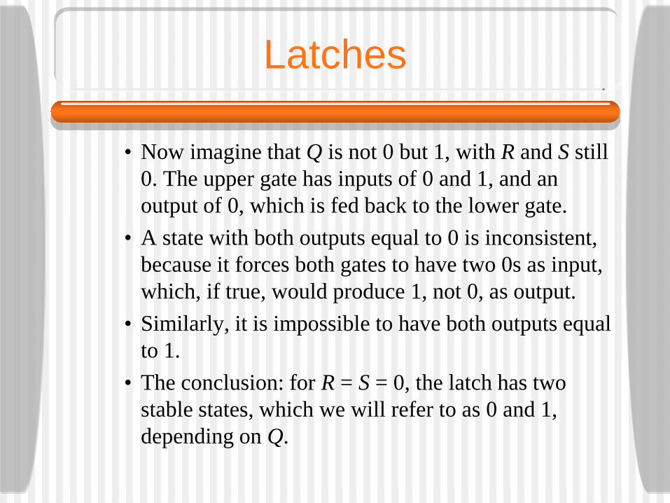
• Now imagine that Q is not 0 but 1, with R and S still 0. The upper gate has inputs of 0 and 1, and an output of 0, which is fed back to the lower gate.
• A state with both outputs equal to 0 is inconsistent, because it forces both gates to have two 0s as input, which, if true, would produce 1, not 0, as output.
• Similarly, it is impossible to have both outputs equal to 1.
• The conclusion: for R = S = 0, the latch has two stable states, which we will refer to as 0 and 1, depending on Q.
Latches
• Now examine the effect of the inputs on the state of the latch. Suppose that S becomes 1 while Q = 0. The inputs to the upper gate are then 1 and 0, forcing the Q’ output to 0. This change makes both inputs to the lower gate 0, forcing the output to 1.
• Thus, setting S switches the state from 0 to 1.• Setting R to 1 when the latch is in state 0 has no
effect.• Setting S to 1 when in state Q = 1 has no effect, but
setting R drives the latch to state Q = 0. The circuit “remembers” whether S or R was
last on.
Latches
It is often convenient to prevent the latch from changing state except at certain specified times. The circuit to accomplish this is called a
clocked SR latch. The circuit has an additional input, the clock,
which is normally 0. With the clock 0, both AND gates output 0, and the latch does not change state. When the clock is 1, the latch becomes sensitive to S and R. The terms enableand strobe mean that clock input is 1.
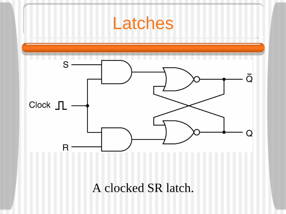
Latches
A clocked SR latch.
Latches
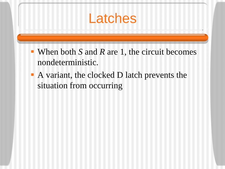
When both S and R are 1, the circuit becomes nondeterministic. A variant, the clocked D latch prevents the
situation from occurring
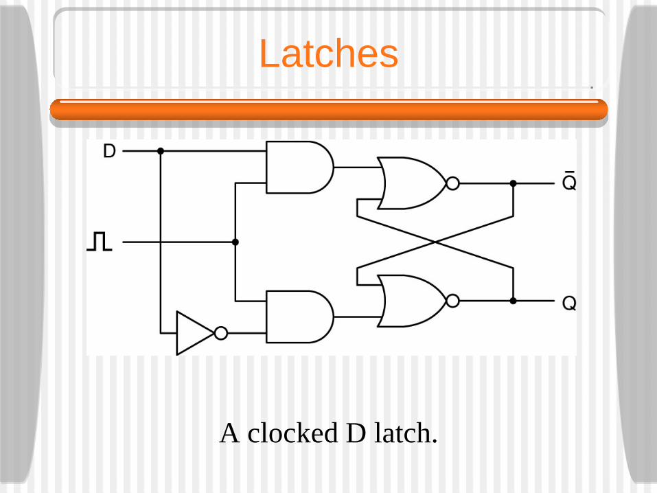
Latches
A clocked D latch.
Flip-Flops
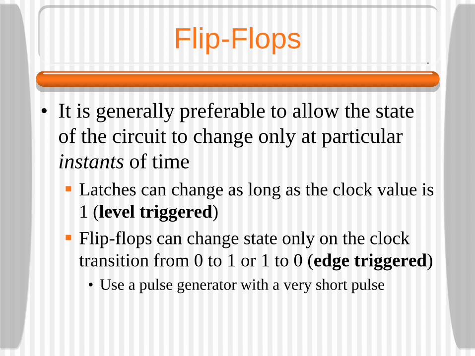
• It is generally preferable to allow the state of the circuit to change only at particular instants of time Latches can change as long as the clock value is
1 (level triggered) Flip-flops can change state only on the clock
transition from 0 to 1 or 1 to 0 (edge triggered)• Use a pulse generator with a very short pulse
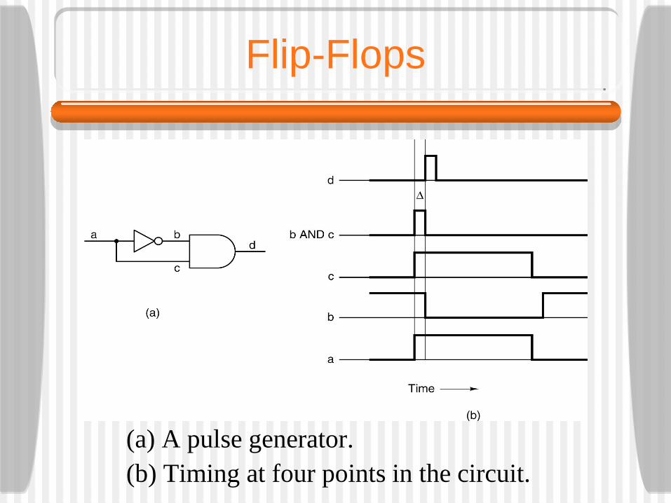
Flip-Flops
(a) A pulse generator.(b) Timing at four points in the circuit.
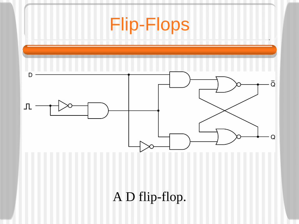
Flip-Flops
A D flip-flop.
Registers
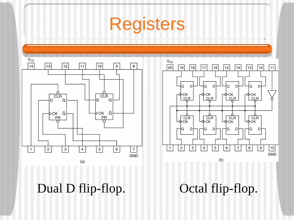
Flip-flops are available in a variety of configurations.
• A simple one with two independent D flip-flops with clear and preset signals is illustrated on the following slide.
• Although packaged together, the two flip-flops are unrelated.
• The second arrangement shows an octal flip-flop in which the eight D flip-flops are not only missing the Q’ and preset lines, but all the clock lines are ganged together and driven by pin 11 so the flip-flops are loaded on the rising transition.
Registers
Dual D flip-flop. Octal flip-flop.
Registers
All eight clear signals are also ganged, so when pin 1 goes to 0, all the flip-flops are forced to their 0 state. While one reason, for ganging the clock and
clear lines is to save pins, the chip in this case is used in a different way from eight unrelated flip-flops. It is used as a single 8-bit register. We can also use two such chips as a 16-bit
register by tying their respective pins 1 and 11 together.
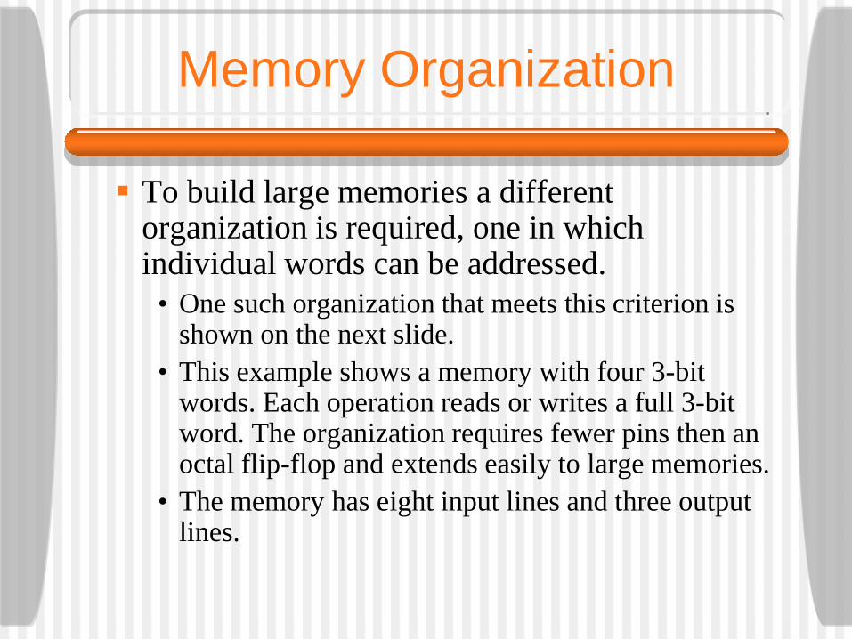
Memory Organization
To build large memories a different organization is required, one in which individual words can be addressed.
• One such organization that meets this criterion is shown on the next slide.
• This example shows a memory with four 3-bit words. Each operation reads or writes a full 3-bit word. The organization requires fewer pins then an octal flip-flop and extends easily to large memories.
• The memory has eight input lines and three output lines.
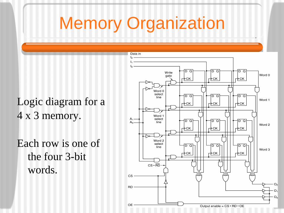
Memory Organization
Logic diagram for a 4 x 3 memory.
Each row is one of the four 3-bit words.
Memory Organization
We could have designed a circuit in which the three OR lines were just fed into the three output lines, but in practice the same lines are used for both input and output. What is needed is an electronic switch that can
make or break a connection in a few nanoseconds. Such a switch is called a noninverting buffer. It has a data in, data out, and a control line. When control is high, the buffer acts like a wire. When control is low, the buffer acts like an open circuit.
Memory Organization
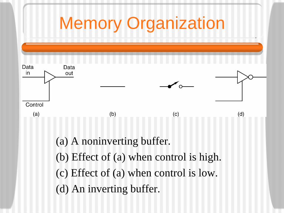
(a) A noninverting buffer.(b) Effect of (a) when control is high.(c) Effect of (a) when control is low.(d) An inverting buffer.
Memory Organization
An inverting buffer acts like a normal buffer when control is high, and disconnects the output from the circuit when control is low. Both kinds of buffers are tri-state devices,
because they can output 0, 1, or none of the above. Buffers also amplify signals so they can drive
many output simultaneously.• They are sometimes used in circuits for this reason,
even when their switching properties are not needed.
Memory Chips
The memory shown previously easily extends to larger sizes. For example, to extend to 4 words of 8 bits
each we add five more columns of four flip-flops each, as well as five more input and output lines. To extend to eight words of three bits each, we add four more rows of three flip-flops each and one more address line.
• For maximum efficiency, the number of words in memory should be a power of 2, but the size of words can be anything.
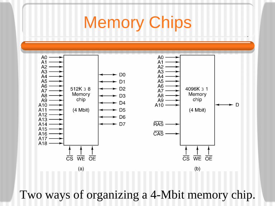
Memory Chips
For any given memory size, there are various ways of organizing the chip. A 4-Mbit chip could be organized as 512K
words of 8 bits each or 4096K words of 1 bit each. Aside - on some pins a high voltage causes an
action to happen while on others a low voltage causes the action. Thus, we will say that a signal is asserted or negated to avoid this issue. A signal S is asserted high, but S’ is asserted low.
Memory Chips
Since a computer will generally have multiple memory chips, a signal is needed to select the chip that is currently needed. The CS’ (Chip Select) signal is provided for this purpose. We also a need a signal to distinguish reads
from writes - the WE’ (Write Enable) signal. The OE’ (Output Enable) signal is asserted to
drive the output signals. When it is not asserted, the chip output is disconnected.
Memory Chips
Two ways of organizing a 4-Mbit memory chip.
Memory Chips
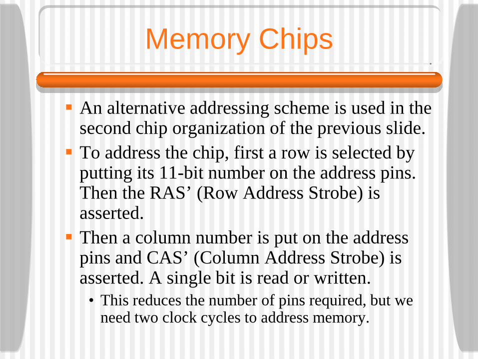
An alternative addressing scheme is used in the second chip organization of the previous slide. To address the chip, first a row is selected by
putting its 11-bit number on the address pins. Then the RAS’ (Row Address Strobe) is asserted. Then a column number is put on the address
pins and CAS’ (Column Address Strobe) is asserted. A single bit is read or written.
• This reduces the number of pins required, but we need two clock cycles to address memory.
RAMs and ROMs
The memories we have seen can be both read and written. Such memories are called RAMs(Random Access Memories). RAMs come in two varieties, static and
dynamic. Static RAMs (SRAMs) are constructed using
circuits similar to the D flip-flop. They retain memory as long as power is on, are fast, and are often used to implement level 2 cache memory.
RAMs and ROMs
Dynamic RAMs (DRAMs) do not use flip-flops. A DRAM is an array of cells, each cell contains one transistor and one capacitor. The capacitors can be charged or discharged, allowing data to be stored. Since the electric charge tends to leak away,
every bit in a DRAM must be refreshed every few milliseconds. DRAMs have a high capacity, thus they are almost always used for main memory. On the other hand, they are slow.
RAMs and ROMs
An FPM (Fast Page Mode) DRAM is organized as a matrix of bits and requires a row and then a column address to be presented. FPM DRAM is gradually being replaced by
EDO (Extended Data Output) DRAM, which allows a second memory reference to begin before the previous memory reference completes.
• Both FPM and EDO chips are asynchronous (the address and data lines are not driven by a single clock).
RAMs and ROMs
SDRAM (Synchronous DRAM) is a hybrid of static and dynamic RAM and is driven by a single synchronous clock. It is often used in large caches. ROMs (Read-Only Memories) have their data
inserted during manufacture. The only way to replace the program in a ROM is to replace the chip. The PROM (Programmable ROM) can be
programmed (once) in the field by selectively blowing fuses.
RAMs and ROMs
The EPROM (Erasable PROM) can be field-erased as well by exposing the EPROM to a strong ultraviolet light for 15 minutes. The EEPROM can be erased by applying pulses
to it rather than UV light. It can also be programmed in place (an EPROM requires a special programming device). EEPROMs are slow compared to DRAMs and SRAMs.
• Flash memory is block erasable and rewritable. They are often used in digital cameras, but they wear out after about 10,000 erasures.
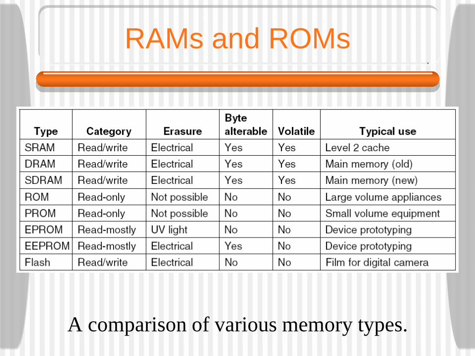
RAMs and ROMs
A comparison of various memory types.
CPU Chips
All modern CPUs are contained on a single chip. Each CPU chip has a set of pins, through which
all communications with the outside world occur. The pins on a CPU chip can be divided into
three types:• address• data• control
CPU Chips
These pins are connected to similar pins on the memory and I/O chips via a collection of parallel wires called a bus. To fetch an instruction from memory, the CPU:
• puts the memory address of the instruction on its address pins
• asserts one or more control lines to inform the memory that it wants to read a word
• waits for a signal from the memory that it has put the data on the CPU’s data pins
• accepts the word and carries out the instruction
CPU Chips
Two of the key parameters that determine the performance of a CPU are the number of address pins and the number of data pins. A chip with m address pins can address up to 2m
memory locations. A chip with n data pins can read or write an n-
bit word in a single operation.• A CPU with 8 data pins will take four operations to
read a 32-bit word, whereas one with 32 data pins takes just one operation. More pins implies more expensive, however.