c)rrIoNEER' - CREAPROMEDIA Sauvegarde du Patrimoine · c)rrIoNEER' ORDER NO. ARP-OO6-O STEREO...
47
c)rrIoNEER' ORDERNO. ARP-OO6-O STEREOCASSETTEDECK MODEL CT-X5O COMES IN FIVE VERSIONS DISTINGUISHED AS FOLLOWS: o This service manual is applicable to the KU type. For servicing of the other types, please refer to the additional service manual. o Cemanuel d'instruction serefère au mode de réglage, en français. o Este manual de servicio tratadel método de ajuste escrito en espafiol. 1. 2. 3. 4. 5. 6. 7. 2 3 4 5 7 15 "17 8. 9. 10. 11. 12. P.C.BOARDS CONNECTION D IAGRAM SHEMATIC DIAGRAM ELECTRICAL PARTS LIST PACKING ADJUSTMENT. REGLAGE ADJUSTE Type Voltago Remarks KU 12OV only U.S.A model r{E 22OYand 24OV (Switchablel Europe model HB 22OYand 240V (Switchabte) U.K. model D 12OV,22OV and 240V (Switchabtel General export model D/G 12OV, 22OV and 24O (Switchablel U.S. military model CONTENTS SPECIFICATIONS FRONTPANEL FACI LITIES. DISASSEMBLY PARTSLOCATION CIRCUIT DESCRIPTIONS. BLOCK DIAGRAM EXPLODED VlEWS AND PARTS LIST 24 27 30 32 33 40 47 PfONEEFI ELECTFICINIC CC|FIPCIFIATIEIN 4-1. .v'esuro I -chome. Meeuno-ku. Tokyo j s3. Jêpân U.a. F|CTNICF| ILICTF|CINICa CCIF|PCIFIAI|CIN BS Oxro.d D.rve. Moonêchre. New Jensev O7O74. US A FlGlNlll| CLCCTFICINIC (É9F|C!FE! N.\/. LurEhegen-Hêven g, 2OSO Ancwenp. E}etgrum FfClNllF lLlCIFlClJ\|lCa AUaTFALIA F1Y. L1Ct. 17A-1e4 Eloundê.v Ftoêd, BnBèsrcte. VrcEoFrâ 31S8. AusE.Êtrs FZ O J ULY 1981 Printed in Japan
Transcript of c)rrIoNEER' - CREAPROMEDIA Sauvegarde du Patrimoine · c)rrIoNEER' ORDER NO. ARP-OO6-O STEREO...

c)rrIoNEER'
ORDER NO.ARP-OO6-O
STEREO CASSETTE DECK
MODEL CT-X5O COMES IN FIVE VERSIONS DISTINGUISHED AS FOLLOWS:
o This service manual is applicable to the KU type. For servicing of the other types, please refer to theadditional service manual.
o Ce manuel d'instruction se refère au mode de réglage, en français.o Este manual de servicio trata del método de ajuste escrito en espafiol.
1 .2.3.4 .5.6.7 .
234
57
1 5" 1 7
8.9.10 .1 1 .12.
P.C.BOARDS CONNECTION D IAGRAM
SHEMATIC DIAGRAM
ELECTRICAL PARTS LIST
PACKING
ADJUSTMENT.REGLAGEADJUSTE
Type Voltago Remarks
KU 12OV only U.S.A model
r{E 22OY and 24OV (Switchablel Europe model
H B 22OY and 240V (Switchabte) U.K. model
D 12OV,22OV and 240V (Switchabtel General export model
D/G 1 2OV, 22OV and 24O (Switchablel U.S. mi l i tary model
CONTENTSSPECIFICATIONS
FRONT PANEL FACI LITIES .
DISASSEMBLY
PARTS LOCATION
CIRCUIT DESCRIPTIONS.BLOCK DIAGRAMEXPLODED VlEWS AND PARTS LIST
2 42 73 03 23 34 04 7
PfONEEFI ELECTFICINIC CC|FIPCIFIATIEIN 4-1. .v'esuro I -chome. Meeuno-ku. Tokyo j s3. JêpânU.a. F|CTNICF| ILICTF|CINICa CCIF|PCIFIAI|CIN BS Oxro.d D.rve. Moonêchre. New Jensev O7O74. US AFlGlNlll| CLCCTFICINIC (É9F|C!FE! N.\/. LurEhegen-Hêven g, 2OSO Ancwenp. E}etgrumFfClNl lF lLlCIFlClJ\ | lCa AUaTFALIA F1Y. L1Ct. 17A-1e4 Eloundê.v Ftoêd, BnBèsrcte. VrcEoFrâ 31S8. AusE.Êtrs
FZ O J ULY 1981 Pr in ted in Japan

5. CIRCUIT DESCRIPTIONSThe main circuit configuration is outlined in the
block diagram on page 15.
5.1 SIGNAL PATHRecording Mode
The input signal from LINE INPUT is passed viathe INPUT volume control, flat amplifier and MpXfilter before being applied to the Dolby NR circuit.
The Doly NR circuit output is then applied tothe recording amplifier equalizer where the fre-quency response is regulated according to the typeof tape being used before finally being appliedto the recording head.
Playback Mode
The playback head output signal is applied tothe playback equalizer (gain 5B.2dB) where thefrequency response is corrected according to thetype of tape being used. Following this, the signalis passed via the MPX filter to the Dolby NRcircuit, and then via the REC/PB switch (HA1200belechonic switch) and MUTE switch (HA12006electronic switch) to the LINE OUTPUT as theplayback output signal.
5 .2 CONTROL CIRCUITThe CT-X50 contuol circuit (outlined in Fig. 5-1)
features a logic IC (8A843) for control of mechani-cal drive by feather-touch switch operations. The84843 pin layout is shown in Fig. 5-1 and theinput/output::i^:"::
:,t:: t""1
"-
Fû Sî6F FF MÊrio ru PA,SE -REc
cNo
Fig. 5-1 Pin arrangement of 8A843
Power-Assist MechanismBefore describing circuit operations during each
operational mode, the basic principles of thepower-assist mechanism will be explained.
Gear return spring Flywheel assembly
Gear leverStopper
Fig. S-2 STOp mode
o Stop Mode1. The cam gear is positioned as shown in Fig. b-2.o Stop Mode to Play Mode (Figs. b-4, b-b, b-6)2. When solenoid P (pinch solenoid) is activatede,
the cam gear stopper is released O.3. The operating lever is then forced down
(direction @ ) bV the operating lever returnspring, and because of the shape of the cam,the cam gear starts to turn in direction @.
4. As the cam gear rotates in direction O . itengages the capstan gear @.
Lever spring
I npu t s i gna lOutput
Output modeU ' T F O . R E W O_RE C O-PAU SE O-PLA Y
S T O P L L L L L STOP modeF F H H FF mode
n L H L L REW mode
P L A Y L L L L H PLAY mode
PAUSE L L L L H L PAUSE mode
R E C / P L A Y L H L H REC/PLAY mode
BEC/P_A_USE L L H H L REC/PAUSE mode
Fig. 5-3 Input/output truth table

Gear return spring Play Mode to Stop Mode (Fig.5-7)7. lilhen switching to stop mode, solenoid P is
deactivated (in direction (D ) and the cam gearstopper released (D. The cam gear rotates tothe stopper position (@, O), and the operat-ing lever is lowered ( (D) bV the operating leverreturn spring, thereby restoring the mechanismto the original stop mode status.
1 Gear return springI C a m q
Flywheel assemblyCapstan
Leverspring
assemblySolenoid P o
Fig. 5-4 STOP + PLAY mode I
5. Once the cam gear engages the capstan gear,the motor and flywheel rotational momentumcontinue to drive the cam gear @ until thestopper reaches the PLAY position 0). lnthis position, the operating lever is pushed up
@due to the shape of the cam.6. At the same time, the operating lever shaft
is raised 0, thereby pushing the HB drivespring attached to the head base upwards toforce the head base into the PLAY position.And since the pinch pressure spring is alsoelevated, the pinch roller is pressed againstthe capstan for start of play.
Flywheel assembly
ICam gear
Gear lever
LeverSolenoid p assembly
Fig. 5-7 PLAY + STOP mode
Tape Transport Mode SwitchingPins 1, 2, 3 and 5 of IC402 (8A834) are the
input pins for PLAY, STOP, FF and REW. Whenany pin is switched to L level, the tape deckis switched to the conesponding transport mode.For example, when 52 and S3 are switched on,pins 1 and 2 of. IC404 are switched to L level,resulting in the OR gate output pin 3 also beingswitched to L level. This is followed by pin 1of.1C402 being switched to L level, thereby switch-ing the deck to play mode. Likewise, SB and 54are switched on for fast forward mode, 52 and Sbfor rewind mode, and 54 and 55 for stop mode.
I
; Gear return springI Cam gear
Solenoid P
Solenoid P
El
Gear lever
Fig. 5-5 STOP -' PLAY mode tl
return spring
Gear lever
Lever spring
Stooær Q
o
f 6 1 5 t 4 t 3 t 2 { t t o 9
tc4o2 8A843
1 2 3 4 5 6 7
Fig. 5-8 Tape transport mode switching
Fig. 5-G STOP-+ PLAY mode ll l

J---_1_UJ.--1/.-ftll
tl
5.3 MUTING CIRCUITMuting Gate
The LINE OUTPUT muting gate is incotporatedin IC401 (H412006), the output being mutedwhen pin 15 of this IC is at L level and pn 2 atH level.
Pin 15 is connected to the PLAY output of theoperating mode control IC (8A843) and is switch-ed to H level only during playback mode. +B isapplied to pin 2 vn R478 and, R477, and the pinis kept at H level except when Q426 is turned onduring recording mode. In this way, the line outputis muted during fast forward, rewind, stop andplay pause modes, and cancelled during playback,recording and recording pause modes.
Fig. 5-12 LINE OUTPUT mutins
The recording amplifier input muting gate isgloundconnected by transistors (Q103 and Q104).The bases of these hansistors are connected to pin2 of HA12006 via R145, R143, R428, D427,D429 and R477, thereby enabling muting to becancelled during recording mode. fhrring rec mutemode, however, these bansistors are turned on,resutling in the recording of blank sections of tape.
BEC AMP
D4æ D427
2.
3 .
r' :L
sroP 1-
vs --J*pg1y
lC4O2Pin 14
Pinch solenoid
Head base
MS solenoid
FF solenoid
1C403 Pin6
1C403 PinS
Fig. 5-10 MS operation timing chart
Auto-Stop CircuitThis circuit is used to switch the mechanical
drive conbol IC (BA843) to stop mode when tapetransport stops (see Fig. 5-11). A photo-intemrpteris used for tape transport detection, and the rotaryblade mechanism used to intemrpt the light beamis coupled to the take-up reel by belt.
During Tape Transport1. Q401 is turned on and off repeatedly by the
photointernrpter output, resulting in C403being charged up and discharged again in re-peated cycles.
When Tape Transport StopsWhen the take-up reel stops at the end of thetape, Q401 ceases switching on and off due tothe loss of the photo-intemrpter output.With a current being passed from +B to C4O3via R405 and R406, C403 is charged up andthe Q402 base potential increases, resultingin Q402 being turned off. Q403 is thus turnedon and pin 2 (STOP) of.tC402 is switched toL level, thereby switching the deck to stopmode.
I C 4 0 2 ( O - P L A Y ,( 4a843'
to( o - R E C )
c402
cr03
F405
i
\
i'iJ
+B (12V1
2( STOP '
I c{02
t4
{5
o{0r
t2
FiS. +t 1 Auto-stop circuit Fig. 5-13 REC AMP mut ing

aMuting at Start of ptayback Mode (Stop 1s p;6r_back Model)
When the tape deckmode from stop mode,mode control IC (BAg4ilevel, and pin 1 of IC4(temporarily to H level
.4 is fully charged up).cancellation of muting-at>de is dêtermined by tt u100ms) of C4}6connect-
is arso added due to ii3î;lil"Tâ1,r.îiï,ii,l#iConsequenfly, line outplî *rù;;l; cancelledapproximately 0.6sec
lfter swidilg t"o ptayuactc*:dg, thereby eliminating tt "
slro"t "nài*u g"rro"t_ed when the head nrakes "ir"t"J
*itrri[" ,"o".
5.4 RECORDTNG MUTING
\qf3IEC/PLA1
O-REC I O.PLAYl r l H
Muting at Start of Recording Mode (Stop to Re_cording Mode)C438 connected to pin g of HAL2006 is atiming capacitor used to regubtÀ trre lperationattiming of the head _switch (the rà"oraing signalshorting relay RyB01 connectea to-pin 6). Whenswitching to recording mode frorn-riop mode,
9jl8 i: charged up, anâ pin 6 switàhed from L ron revel once the capacitor has been charged up.ïVhile this C4Bg is--being
"fr*eàJ "p (approx.
200ms), the LINE OUTPU"T i, *-,itua. ôat is mut_ing is cancelled after a delay of abàut 200ms,thereby eliminating switching "tir".
---
F i s . 5 - 1 4
Fig. 5-15 Muting at start of recording
FiS. S-t0 Recording muting
This function is employed in preparing blanksections of unrecor.l-eà iupu ,"ffi"a for MS(automatic location .ot. stari'or t."""]]bi"" e e426Q427 arc both on durir
------l' I
99t-di"g amplifier input(41.03 and e104) areremrans unmuted. If Siswitched on, e10B and (passed via SB, D426.Q103 (Q104). The .u"o*attenuated, and tape harany signal being reco_rded. At the same time, +B i6lJro pur:g9 via SB, R480 and isorôz b e426,jf,i"glv let'ting up rhe REC Mu-T-E-i;icator lamp(LED507).
BEC AMP
lc 4Dt (HAI2OO6)
Muting at start of playback

4. PARTS LOCATION
Front Panel ViewKnob A (T lMER l
RAC-170
Eject knobRAC-164
NOTES:o Parts without part number cannot be supplied.o The ;i. marh found on some component parts indicates the importance of the
safety factor of the part, Therefore, when replacing, be sure to use parts of identicaldesignation,
o For your Parts Stoch Control, the fast mouing items are indicated with themarks ** and t** GENERALLY MOVES FASTER THAN *This classification shall be adjusted by each distributor because it depends on modelnumber, temperature, humidity, e tc.
BonnetRNA-549
B ( R E C }RAC-21 5
f
I
)
nct ion knobRAC-2|3
Knob D (DOLBY NR)RAC-l68
C (REC MUTE)RAC-216
Knob A (PAUSE)RAC-214
t t Push switchRSGO88
Function switch assembly
* * Push switchRSG- I 14
* * Pinch arm assemblyR8H-760
l \ Strain ret iefREC-272
A CoroRDG.O22(BDGO30)
* t Door assemblyRX8.594
Power knobRAC-163
Knob C (MUSIC SEARCH)RAC-172
Knob B (REC/PLAY)RAC-171
Front View with Front Panel Removed
CounterRAW.159
Cassette plate assemblyRXX-325
* Erase headRPB-085
* * REC/PB headRPBO84
Rear Panel View
Term ina l ( L INE)
R KB-o18
* Variable resistorRCV-093
Pin jack
RKN071
5
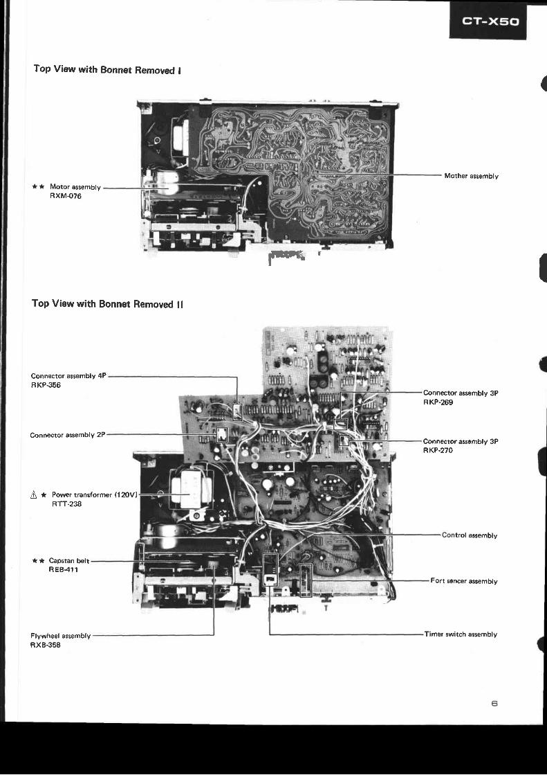
Top View with Bonnet Remoræd I
I * Motor assemblyRXM-076
Top View with Bonnet Removed ll
Connector assembly 4PBKP.356
Connector assembly 2P
[ * Powertransformer (120V1RTT-238
* * Capstan beltREB41 . I
Flywheel assemblyRX8-358
r
Mother assembly
connector assembly 3PRKP.269
Connector assembly 3PRKP.27O
trol assembly
Fort sencer assembly
I
{
Timer switch assembly

When the Pornær is Switched on (See Fig. 5-91When the power is switched on, +B is passed via
C4O4 and R415 to Q40G, being turned on forabout 1.5 to 2.5 seconds (until C404 is fully charg-ed). This results in pin 2 (STOP) of IC402 beingswitched to L level, thereby ensuring that the deckis orginally in stop mode. If any other switch ispressed during this initial brief period, the deckwill remain in stop mode. +B will, however, beapplied to the capstan motor and the motor willstart up.
Playback ModeWhen the PLAY switch (S2/SB) is pressed, pin 1
(PIÂY) of. tC4O2 is switched to L level and pin 12(O-PLAY) to H level. +82 is thereby passed viaF"423 and R424 to Q410, rezulting in this transist-or being tumed on. The pinch solenoid SOL isconsequently activated and playback mode com_menced (see Power.Assist Mechanism).
Recording Mode1. Iilhen a cassette half with the erasure preven-
tion tabs intact is loaded into the deck (result-ing in the erasure prevention switch S10 beingswitched to the NO HOLE position) and SZswitched on, pin 10 (O-REC) and pin 12(0-PLAY) of.IC4O2 switched to H level.
2. The pin 10 output is applied to the base ofQ426 vira R481. With e426 turned on, pin 2(REC signal input) of. IC4OI is switched to Llevel. And since pin 12 is at H level, pin 1b(PLAY signal input) of IC401 is switched toH level resulting in pin 6 (head switch) and pin16 (recording/playback switch) of IC401 alsobeing switched to H level. The recording inputshorting relay RY301 in the record/playbackhead circuit is opened and the playback outputshorting transistor Q101 is tumed on (therebyswitching the head to recording mode).
3. With'pin 10 of IC4O2 and the playback outputshorting transistor Q301 is turned on and thebias oscillator activated.If a cassette half without the erasure preven_tion tabs is loaded, S10 is switched to theHOLE position, resulting in pin g (À-R) ofIC4O2 being switched to L level. In this state,the tape deck will not be switched to recordingmode when pin Z (EE-C) is switched to L level.
Fast Forward ModeWhen the FF switch (Sg/S4) is pressed, pin 1b
(0-FF) of. 1C402 is switched to H level, reiultingin +32 being passed, to e40T via R4LT and R41g.And once Q407 is tumed on, the FF solenoidis activated to start fast forward mode.
Rewind ModeWhen the REIV switch (S2lSb) is pressed, pin
13 (O-REW\ of.lC4O2 is switched to H level, result-ing in +82 being passed to Q408 via R420 andR42L, thereby turning Q408 on to activate theREW solenoid for start of rewind mode.
Time Playback ModeTape playbaek is started automatically at the
time set by the timer.1. I{hen the power is switched on with the
TIMER switch S11 on and S12 set to play, +Bis immediately passed to Q411 via C406 andÈ426, thereby tuming Q411 on for about B to5 seconds (until C406 is fully charged). Inaddition, +B is applied to Q406 via C404 andR415, resulting in Q406 being turned on forabout 1.5 to 2 seconds (until C404 is fullycharged). As a rezult, pin 1 (Pf,Ây) and pin 2(STOP) of.IC OZ are switched to L ievel.
-
2. lflhile pin 2 remains at L level, stop mode haspriority over all other modes, and pin 12(O-PLAY) of. 1C402 is switched to L level.
REC/PB head
ry o!0.+B3
oscBLOCK
3. Q406 is turned off once C404 has been fullycharged up, resulting in pin 2 of.l0402 bengswitched to H level (L + H). Since Q411 ison at this time, pin 1 of ICAOZ will be at Llevel, and pn 72 will be swiôched to H level(L - H). Q410 will thereby be turned on,and the pinch solenoid SOL activated as des-cribed above for playback mode.
Timer Recording ModeThe tape deck is started up automatically in
recording mode at the time set by the timer.1. \[hen the power is switched on with the
TIMER switch S11 on and S12 set to REC,Q406 and Q411 are turned on for severalseconds in ttre same $'ay as described abovefor timer playback mode. As a result, pin 1(PLÂY), pn 2 (SIO=P) and pin ? (EE-C) ofIC402 are all switched to L level.
2. During tlre period that pin 2 of. IC4O2 is atL level, pin 10 (0-REC) and pin 12 (O-PLAY)of the same IC are also at L level.
3. Once C404 is fully charged, Q406 is turnedoff, resulting in pin 2 of.lC4O2 being switched
to H level (L + H). And since pins 1 and ? ofIQ402 are at L level at this time pins 10 and 12are switched to H level (L + H), therebyresulting in the start of recording mode (seenormal recording mode for further details.
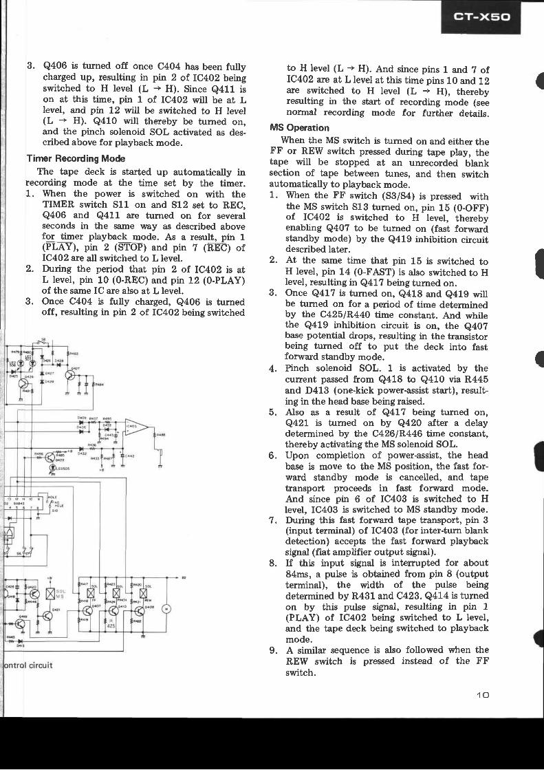
MS Operation\{hen the MS switch is turned on and either the
FF or REW switch pressed during tape play, thetape will be stopped at an unrecorded blanksection of tape between tunes, and then switchautomatically to playback mode.1. \{hen the FF switch (S3/S4) is pressed vdth
the MS switch S13 tumed on, pin lb (O-OFF)of IC4O2 is switched to H level, therebyenabling Q407 to be turned on (fast forwardstandby mode) by the Q419 inhibition circuitdescribed later.At the same time that pin 15 is switched toH level, pin 14 (0-FAST) is also switched to Hlevel, rezulting in Q417 being turned on.Once Q417 is tumed on, Q418 and Q419 willbe tumed on for a period of time determinedby the C425|P"44O time constant. And whilethe Q419 inhibition circuit is on, the e40Zbase potential drops, resulting in the transistorbeing turned off to put the deck into fastforward standby mode.Pinch solenoid SOL. 1 is activated by thecunent passed from Q418 to Q410 via R445and D413 (one-kick power-assist start), result-ing in the head base being raised.Also as a result of Q417 being turned on,Q421 is turned on by q420 after a delaydetermined by the C4261R"446 time constant,thereby activating the MS solenoid SOL.Upon completion of power-assist, the headbase is move to the MS position, the fast for-ward standby mode is cancelled, and tapetransport proceeds in fast forward mode.And since pin 6 of IC403 is switched to Hlevel, IC403 is switched to MS standby mode.During this fast forward tape transport, pin 3(input terminal) of IC403 (for inter-turn blankdetection) accepts the fast forward playbacksignal (flat amplifier output signal).If this input signal is intenupted for about84ms, a pulse is obtained from pin 8 (outputterminal), the width of the pulse beingdetermined by R431 and, C423. Q4L4 is tumedon by this pulse signal, resulting in pin 1(PLAY) of. îC4O2 being switched to L level,and the tape deck being switched to playbackmode.A similar sequence is also followed when theRElfl switch is pressed instead of the FFswitch.
I
I2 .
3 .
4.
5 .
I
6 .
7 .
8.
9 .
1 0

5.5 FUNCTION SELECTORïVhen ttre CT-X50 is used with the A-X30 or
A-X50, this function selector circuit passes signalsto the A-X30 or A-X50 indicating the tape deckoperational status.
IC405 (M51202L) receives output signals viadiodes D409, D408 and D432 from different1C402 (8A843) output pins during different opera-tional modes. During playback, fast forward andrewind modes, pin 1 of IC405 is at a higher po-tential than pin 2, resulting in pin 3 being switchedto L level. If t'Lre deck is then switched to record-ing mode, the D432 cathode is switched to H leveland the D409 and D408 cathodes are switched toL level. with the D432 cathode at H level, pin 2 ofIC405 is switihed to a higher potential than pin 1,resulting in pin 3 being switched to H level. Pin 3is also switched to H level during stop mode dueto +B being applied to pin 2. C443 and C442have been inserted in order to prevent misopera-tion during mode switching (use is made of thetime constants of these capacitors during each typeof mode switching).
5 .7 T IMING CHART
MS MODE
O- PLAY
O-FAST
O-REC
+ B
Fig. 5-1 7 Function selector
5.6 AUTO TAPE SELECTORTape selection of normal, chrome and metal
tapes in the CT-X50 is performed automaticallyby detecting special detector holes in the respec-tive cassette halves. The presence/absence of theseholes is detected mechanically by S14 and S15.Depending on the rezultant switch combination,the required supply voltage is applied to theoscillator circuit in order to obtain the appro-priate bias level for each type of type.
STOP MS MODE PLAY
FAST SIGNALlC 8A843 Pin14
PINCHSOLENOID
HEAD BASE
MS SOLENOID JF F S O L E N O I D
REW SOLENOID
MS MUTINGlC 8A336 Pin 6
MS PLAY PULSlC 8A336 Pin 8

NORMAL OPERATION
CHANGE
POWE RON P L A Y STOP
F F o rR E W STOP
Kèç,/
P A U S EREC,/
P L A Y STOPREC./
P L A Y STOP POWERO F F
J(J
PINCHSOLENOID
ON
I FoFF
=t-1caI>OCî.JJ
TAPETRANSPORT J J J
IELtJtt-J-
LINE OUTMUTING _,r-I I IREC AMPMUTING -.,r I IPOWER SWON/OFFMUTING
_,rlBIASOSCILLATOR J \ / \
*- . ,Ë
sg9POWER SWON/OFFMUTING
_,rlFUNCTIONSELECTOR J
FF o r REW P L A YREC./
P L A YF F o r
R E W7EC,/
P L A Y
J
O >zy.t*6âà
) I N C H
}OLENOIE
TAPETRANS-PORT J
(rlutr=
L I N E O U TMUTING I I t_REC AMPMUTING
BIASOSCILLATOR l l
AUTO START AUTO STOP
P L A YJ T A N D B Y
i( È.uSTAND P L A Y REC/
P L A YF F o r
REW
J
at f< F1 . U( J >u J v
] I N C H
SOLENOIE î_l- î_I-r
TAPETRANS-PORT _f J L L tï
uJ
EJ
LINE OUTMUTING Jl _r-IREC AMPMUTING J- 11 _f
BIASOSCILLATOR iJ

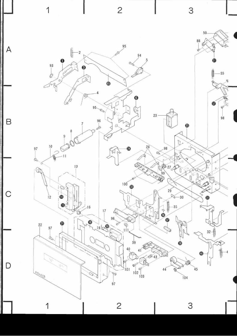
o7. EXPLODED VIEWS AND PARTS LIST7.1 EXTERIOR
t4
t5
aI
iI
I
A
B
o-I
(EC
t3
@D
32
@
{
25
4
o. 1
lt' II
l az
Il i
\

(D
M
ff"q'-''
I

( i . BLOCK DIAGRAM
REC/PB HEAD
L rx€rLPuT
EO AMP
i'ïI
E H E A D
L C h
R c h
MS CIRCUIT
S I : P O W E R5 2 , 3 : P L A Y5 2 , 5 : R E W5 3 , 4 : F F
O N _ O F F
O N _ O F FO N _ O F F
O N - O F F
5 4 , 5 : S T O P5 6 : P A U S E) / n c u
5 8 : R E C M U T E
O N - O F F
O N - O F F
O N _ O F F
O N - O F F
AUTO STOP
S I O : E
S I I : T
S I 2 : T
t L t u z
D O L B Y N R
O R E C
F
É:
M U T IS W iâ--
!1,13.1.;
osc

I-POWER SUPPLY-r
+83+82
+ B l
AC 120v5O/60H2
AUTO FUNCTION CIRCUIT0.o9 Ra37 R493
C1.2
SOLENOID DRIVE CIRCUIT
MOTOR
N BP R E V E N T
O N - O F F
HOLE_NO HOLE
O N - O F F
P L A Y - R E C
S t 3 : M S O N - o F F
S l 4 : T A P E S E L E C T O R N O B M - C r O '
S t 5 : T A P E S E L E C T O B C r O " - M E T A L
ALC CIRCUIT
MUTING
I C 4 0 l
1 6 t 5 t 4 t 3 t 2 i l t o 9I C 4 0 2 8 A 8 4 3
O R
1 E

Part List
Mark No. Part No.
NOîESro Parts without part number cannot be supplied,o The ! marh found on some cornponent parts indicates the importance of the
safety factor of the part. Therefore, when replacing, be sure to use parts of identicaldesignation.
c For your Parts Stoch Control, the fast mouing items are indicated with themarhs ** and *** GENERALLY MOVES FASTER THAN *This classification shall be adjusted by each distrtbutor because it depends on modelnumber, temperature, humidity, e tc.
Description No. Part No, Description
* t
i *
* *
* *
* ** f
1. RNA-5492. RXB-5943. RAW-ls94. REB4445.
GP4i 1B
RBH€34RNHO27
11. RAC- I6412. RX8-50313. RAC-16314. RBH83115. RBH835
BonnetDoor assemblyCounterCounter beltPhoto sensor assembly
Sensing holderPhoto interruptorSensor P.C.B.Eject springEject plate
Eject knobFront panel assemblyPower knobKnob spr ing APlate spring
lndicator lense
Knob AKnob BKnob CKnob D
Knob spr ing BFunct ion knobMechanism assemblyCapacitorCapacitor cover
Power switchTimer switch assemblyPush switchTimer swi tch P.C.B.
Select knob A
Select knob B
S€lect knob CPanel stay
Function switch ass€mblY
LED holder A
LED holder BL E DL E DPush switchPush switch
RTT.238
RDGO22(RDGO3oI
REC-272REC-355REC-369
RNL.223
RKP.269
RKNO7lRKBO18Rcvo93
vcz30P060FMcPMZ3OPOSOFMCRBFO56BMZ3OPO6OFMCvcz30Po80FMC
PMZ3OPOSOFMCvBZ40PO60FMCvcz30P060FzKVBZ3OPOSOFZKRKP.27O
71 . R KP-356
Power transformer (1 20VlNu tMain chassisTerminal (GNDI
Power cord
Strain relief
Slide stopperFoot assemblyRear panel
H inç
Mother assemblyConnector assembly 2P
Connector assembly 3P
Control assemblyHeat sink
JackTerminal (LINE)
Valiable resistor 20k-ASide frameBottom plate
ScrewScrewWasher
ScrewScrew
ScrewScrewScrewScrewConnector assembly 3P
Connector assemblY 4P
* 41 .42.43.44.45.
6 .7 .8 .L
10.
46.47.48.49.50.
5 1 .52.53.54.55.
56.57 .58.59.60.
6 1 .62.63.64 .65.
66.67 .68.69.70.
1 6 .1 7 .1 8 .1 9 .20.
RAC-214RAC-215RAC-216RAC-l68
21. R BH-83222. RAC-21323.24. RCG-00625. REC-247
RSA-046
RSG-1 15
RCA-1 70
RAC- l71RCA-172
RNL.228
RNL-229GL-9PG4GL-9PR4RSG-1 14RSG-088
26.27.28.29.30.
3 1 .32.33.34.35.
36.37.38.39.40.
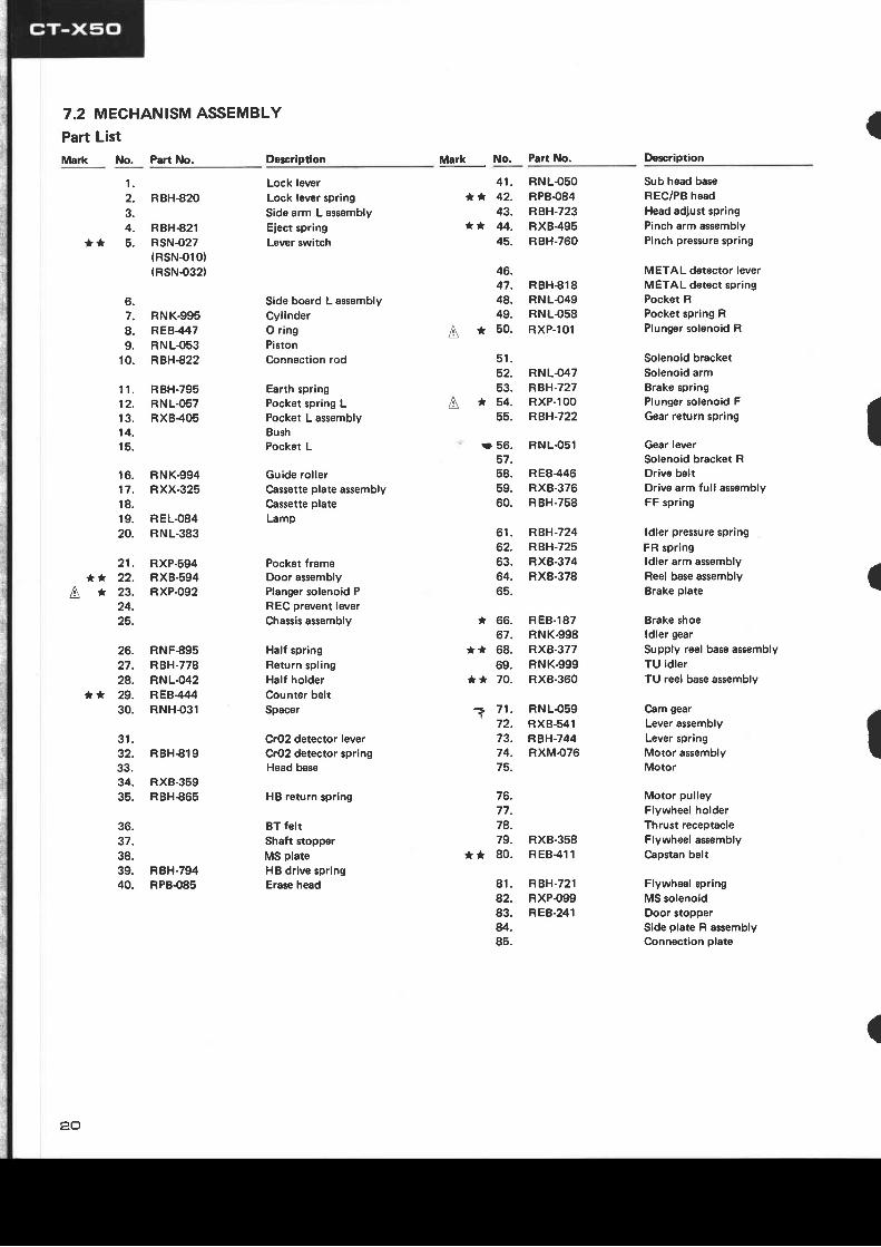
7.2 MECHANISM ASSEMBLY
Part ListMalk No. Part No.
IDoscription Mark No. Part No. Description
t .2 .3.4.5.
3 1 .32. RBI{€1933.34. RXB-35935, RBH€65
36.37.38.39. RBH-79440. RPBO85
Lock leverLock lever springSide arm L assemblyEject springLever switch
Side board L assemblyÇylinderO ringPistonConnection rod
Earth springPocket spring LPocket L assemblyBushPocket L
Guide rollerCassette plate assemblyCassette plateL€mp
Pocket frameDoor assemblyPlançr solenoid PREC prevent leverChassis assembly
Half springReturn spl ingHalf holderCounter beltSpacer
Cr02 deteclor leverCr02 detector springHead base
HB return spring
BT feltShaft stopperMS plateHB drive springErase head
41.* * 42 .
43.* * 44 .
45.
46.47. RBr{€1848. RNLO4g49. RNLO58
* 50. RXP-101
5 1 .52. RNLO4753. RBH-727
* 54. RXP-10055. RBH-722
e 56. RNLOS157.58. REB44659. RXB-37660. RBH.758
61. RBH-72462. RBH-72563. RXB-37464. RXB-37865.
* 66. REB-18767. RNK-998
** 68. RXB-37769. RNK-999
r* 70. RXB-360
a 71 . RNLo5972. RXB-il173. RBH-74474. RXMO7675.
76.77.78.79. RX8-358
r* 80 . REB41 1
81. RBH-72182. RXPOgg83. REB-24184.85.
Sub head baseREC/PB headHead adjust springPinch arm assemblyPinch pressure spring
METAL detector leverMETAL detect springPocket RPocket spring RPlunçr solenoid R
Solenoid bracketSolenoid armBrake springPlunçr solenoid FGear return spring
Gear leverSolenoid bracket RDrive beltDrive arm full assemblyFF spring
ldler pressure springFR springldler arm assemblyReel base assemblyBrake plate
Brake shoeldler gearSupply reel base assemblyTU idlerTU reel base assembly
Cam gearLever assemblyLever springMotor assemblyMotor
Motor pulleyFlywheel holderThrust receptacleFlywheel assemblyCapstan belt
Flywheel springMS solenoidDoor stopperSide plate R assemblyConnection plate
RBH€20
RBH€21RSN-027(RSNO10)(RSN.o32)
RXP.594RX8.594RXPO92
RNF€95RBH-778RNLO42REB444RNHO3l
RNLOsORPBO84RBH.723RX8-495RBH.760i *
21.** 22.
A * 2 3 .24.25.
26.27.28.
*r 29.30.
6.7. RNK-9958. REB447L RNL{53
10. RBHAz2
11. RBH-79512. RNL-O5713. RXB40514.1 5 .
16. RNK-99417. RXX-3251 8 .19. RELO8420. RNL-383
,4\
IA
I
I
I
20

r05
52
54
5
III
)
-a' l95
o
a
(

I718
l c 4 o 2 I C 4 O I
Q426 Q420
I
C O N T R O L A s s ' Y
A
e e l c o t ,
i j ; i Î : ' , l l$ * ; | , 1 : ' I r47ot?s
6 .ô ,
o b o- t.o ' l
f ; ' ; ' l i .
oTP.4'";
;',*fl , ' *__1..
,'T'"jJ*" ozZK
,I,,.+,{ \*,, T ooo''t,
J , f :r, ,X"'.1:j ,;': J:':'.':i I ."' : ' 'ti i'i'"*li - l;1,îË?-;ii.. '-;
. iù - ù4
R4zB D419-1 x 1 5 2 4 : + ".,"J 'Y ,..,.; ;1,"ï;Â;l +'ô'
I l oqtto ':1". ô Q4?? -425' / S L r 7 4 O L N - R o r S B
,ffi'."rjtj'jffii'îi'îhkE-iî.'pi-ifîç-[
I , T lool loL ' f ls o eczz-qzs 'ô s t - -=+ 1 é)Lr /av-nr
Daz6 )+?7 1
lY li?r -,.a 4 t 7 L a ^
R q r o 4 . / f . ^ ? q*+ç+ | 406 /r I
9 . F
10'3
! t pi2 r,'c
D,,r o - 'ler l' ' ii J'i.Xl*,*f L'* " tC .<
I o qRa+r ôr o /u 6. (agtf
D4.6 --
J- -
rl to" on,,i Lt
^ '.1 æ '$ffi1r '" 47/ta"- : ï - - r l - ) r qT + l11 /T_ f " " i r ro o o L l o o o o o o o ï " " " - À " A r l l + ' 1 1 Â ' j i f 1 É - r
C
D
IB7

Mark No. Part No. Description No. Part No. Description
86.** 87. RSHOsg
88.89.90.
91 .92. RLB-39093. YE3OFUC94. PMZ20P080FMC95. VCZ20P060FMC
96. VCZ26P090FMC97. ATZ26PO60FZC98. PMZ26P030FMC99. YE4OFUC100. Pcz26PO60FMC
{b
Detect assembly
Slide switchMount ing plate
Side arm R assemblyElect lever
Stopper leverStopperWasherScrewScrew
ScrewScrewScrewWasherSCREW
101. PMZ2OP13OFMC Screw1O2. IMZ2OY12OFMC Screw103. PMZ2OPI2OFMC Screw104. YE2OFUC Washer105. PMZ26P060FMC Screw
106. YS2OFBT Washer1O7. WAl7D032D025 Washer108. PMA26P040FMC Screw109. WA21D040D025 Washer110. RBF-051 Wahser
111. RBF-050 Oi l s topwasher112. PMA026P040FMC Screw
I)
1

External Appearance of Transistors and lCs
I FESISTOaSIrd{& in {1, {[ :5* rùæ. unb olb.Bb æid I i ro,
u : M r l ( F l : ! t % { G l : ' U { K ) : ' r @ . , ( M : æ % r o l . r . @
2 CAPACITOFSIldidd 'n c*ny llFllvoh4 tv) u.ldorh.ùiÉ6td p: pF
ldrc.rio sir@i voh4 is ry dcæt .lærrolYtÈ cæætor
3 VOI'AG€
ll Dc @hç (vl .r ho inNr ifd
4 OTH€BS]
A :Mjùn iqÈ in lthe
 d* tdd on m mFffir Èni idd6 6e [email protected] ol rh shy læro. ot rh.Fn. lbator.. tu r@tæiq,Erru bu4 Fftol &nrÈ.|tuiFnbn
25A826LN2SC1740LN
HAl200584843
I
-5 STTCHES:
S ' ] PMR52,5 : ÈAYæ t 5 1 E Ws3r4: F9 .5 : sToP56 : PNSE57 : REC$ ; F€C ilUE5 9 i r u Y N R
oN - 9Efd - t r FO - O F Fo -otrO N . 9 E
ON - OFFSlO : EN æWNÎEEM HglE - NO ff5 I I : T IMER ON - GFSI2 : TIMER PUY - æCs l 3 i M s fr -otr
NOTE:Playback signal routeRecording signal route ---
25A11272SC2634
HO?432
2SC2060
Typc No
84336
25D837 HA1t226HAl2006
Lot No
2SD103t M51202L
Type No
NOTE:The indicated semiconductora are repreæntative onesonly. Other alternatiue semiconductons may be used andare listed. in the parts list.
Sl4 I TAÆ SEECTæ tw-C.O2SI5 : TÆE SEÉCIG C.O? -MfrAL
ft. udêilid 'did6 rh.*ùcô Fibn
Thi! ir thé bÉ Sd.rÈ diq.ù, tur rhe ætu.t ci@n hry v.rydu. to 'dFrNdrs in ù'9
E
I7
B ld r

Mark Part No. Symbol & Description SWITCHMark Part No.* wz-135
* BZ-O50
t s2vc10F* 152473
OTHERS
Mark Part No.
zvo2zuol
D,410,D4110418
SymM & Decription
Symbol & Deccription
** RSGO88t* RSG- I 14
Tirner Switch AsæmblySWITCHMark Part No.
s2-S8s9
Symbol & Description
RKB.OI8RKN{71
Function Switch AssemblY
Terminal (l NPUT/OUTPUTIPinjack
Symbol & Deccription
*rt RSG-I 15
Photo Senser Assembly
Mark Part No.
sl 1-sl 3
Symbol & DæcriptionRESISTOR
Mark Part No.* * G P 4 1 1 B
RDî/4PM 1O2J
Detect AssemblyMark Part No.
R601
Symbol & Description
A RDl/2PSF 561J
SEMICONDUCTORS
Mark Part No.
R501-R504
Symbol & Description* r RsH-059
R KP-356Slide switchConnector assembly 4P
11. PACKINGMark No. Part No,
* GL.gPG4r GL.gPR4
LEDsOl-LED5O5LED5O6,LED5O7
Description
1. RHG4262. RHA-2333. RHX-0324. RDEO525. RRB-145
Packing casePad
Sheet DConnection cord assemblyOperating instructions


I 2 IDIAGRAM
3
A
8. P.C. BOARDSCONNECTION
1c201 Q202 lc1 Q l 0 r r c 1 0 1
B
M O T H E R A s s ' y
Q 2 o 4 Q 1 o 3 o 1 o 4 Q 2 o 3Q207 Q206 Q205
V R 1 O 2 V R 2 O 2 L 2 0 3 L l 0 3 L l O 2 L 2 O 2 V R J O 3 V R
C
Q r o 2Q1 07
a r 0 5v R 3 0 t v R t o l
D
321
tT
1
, lJl l
t l l li i l ,
î6S 3ç V R z a{ t 5 " r x
""tt
J Ti,'l:
Cztsi 0 0 P :
v RzcaI50K 8
VRrû3t50K-B

19. SCHEMATIC DIAGRAM
32
I MOTÆR A3S''
--J
A
-
ËH-.
B
c
D o4q,9,462S!74N-R or S d2SC26tr^ Ror S
321
apr,2û2SlÉot-Ror S dææg-R orsS W T C B r c ( R E C . O N )
rc lo r ,æl HAl2æ5RÊC/PB SYSEM C
d 2sc26g-Rorss w r c a r i l G { R E C ' O N )
COtfrROL Ass'y
rc40tHAr2@6MUTING B SWITCH]rc
M22\4252SCl74OLN- R 6S
t-I
II
L-25ÂæU-orR or2$l lz- R d S

654
oroj ,zotlX34A or lX@ or OÂ9O
o4t2,414 ,415ts2473
a
LEO5Oia 5O5oL-9re4
I LEffi,æ7
L:ii_
o 4 t 6 , 4 r 7 , 4 5 1lK34A or lK@A o. OA9O
Q42e?SCl74OLN -R o . s dzscæs-RdS
654
æ3- iO7, æ3 ! 2O72SCI74OLN-R ù S d2Sc2634-R or S
ar03,r@,2o3,2o4Swl rcHl rc (P B -ON)
o!05,26
OUTPUT I
l ;.u ) | R45o-'
I o4oz,4oa,41o| 2sc2m-odR
- - -------J O4O9 O4ilQ4O9 O4il2SCi74OLN-RorS 6 zæ?ru-RdS d2SC26Y-RôrS 2SC2634-RdSa - j - , r r r ! J T r , : M -
t-." ÀÉ.:
2SCt74OLN-RorS d2ææ34- R dS

Part No. Symbol & Description SWITCH
Mark Part No.* wz-135* BZO50
r s2vc10F* 152473
OTHERS
Mark Part No.
zvo2zvol
D410,D411D418
Symbol & Description
Symbol & Dercription
** RSGO88** RSG- I 14
Timer Switch AssemblyswtTcHMark Part No.
s2-s8s9
SYmbol & Description
RKBO18RKNOTI
Function Switch AssemblYRESISTOR
Mark Part No.
Terminal (INPUT/OUTPUT)Pinjack
Symbol & Description
* * R S G . I 1 5
Photo Senser Assembly
Mark Pan No.
sl 1-S1 3
Symbol & Dccription
l!\ RDl /2PSF 561J
SEMICONDUCTORS
ll/lark Part No.
R501-R504
Symbol & Description
* * G P 4 1 1 BRDl/4PM 1O2J
Detect AssemblyMark Part No.
R601
S]'mbol & Dercription
11. PACKINGNo. Part No.
r GL.gPG4t GL.gPR4
LEDsOl-LED5O5LED5O6,LED5O7
Doscription
** RSHOsgRKP.356
Slide switchConnector assembly 4P
1 .2.
RHG426BHA.233
3. RHXO324. RDEO525. RRB-l45
Packing casePad
Sheet DConnection cord assemblyOperating instructions

I nEs ts l0Rs:ldbrd in A ZW !5S tol.ræ u.l6 olh.Mi* mrd k t9,
M : Mo, lF l ' l% lc l I ' 2$ {x , i rO. , t , !æ% rorÙ.æe
2 CAPACIIOFSlldÉùd h csiiY {!Fl/d(ç (Vt ùd6ot@U mtd o I gF
rdtdion whh@t rcnç i3 æv.!c@t êlærolYtb c+æior
3 VOLIAG€
E : æ É t ç l v ) . t É i F r t i F l
. O 'HEÂS:
A : eiuli4 æinrrh. /h m..r l@d d m mæ6r Ènr dt6 th. 'm
FilEa ol ft eey læto. ol rtu M. Tkçl@,ùrdæiq,h ræ burFnso l ûn tÈ. lddgn i l 'on
2SA826LN2SC1740LN
HAl200584843
-5 STTCHES
5I : PMR52,3 : P l^Y
52,5 reW
ON - OFFo -trFs - o fd -gEE
9,5: sloP oN - gfE
56 : PAUSE57 : FEC
$ . REC MUE
oN- f f i
O N - 6 F59 : OCBY NR q -gqEsro EN æwNrmcu HglE - @.!9!Esfi T|MER ON - 9fE5i2 : TIMER PLAY _.æqs r 3 : M S oN -otr
NOTE:Playbach signal route
-_-Recording signal routeSl4 rff i SEÉCTG W-C.O2
Sl5 : IPE SEÉCTæ ç!93 - GTAL
lhuùlid idic.G rhe *i ld æ.iton
Thk is th. bb æh6.i. diqrh br r6a æùd ci@n Êv v.ry
dù. ro inÈdmnc in 6iS.
I7
25A11272SC2634
HD7432
L o t N o
zSC2(b0
Typ. No
8A336
25D837 H411226HAt2006
2SD1031 M512o2L
lype No
NOTE:The indicated semiconductorc are repreæntatiue onesonly. Other alternative semiconductora may be used andare listed in the parts list.
L J
-
1O. ELECTRICAL PARTS LISTNOlES:o When ordertng resistorc, first convert resistance wlues into code form æ shown in
the following examples.Ex. 1 When there are 2 effectiue digits (any d.igit apart from 0), such æ 560 ohm
and 47h ohm (tolerance is shown by J=5%, and K=10% ).560f) 56 x 1014 7 h a 4 7 x 1 0 3
5 6 1 . . . . . R D % P S E B E J473. . . .. RD%PS EAPIB J
o . s a 0 R 5 . . . . . . n N 2 r l [ Ù E B Kr o 0 1 0 . . . . . . R S I P @ n @ K
Ex. 2 When there are 3 effectiue digits (such æ in high precision metal filmresistorc).5.62ko 562 x 10 ' 5621 . . . . RN'/SR EltrEE r
o The I marh found on some component parts indicates the importance of the
safeti factor of the part. Therefore, when replacing, be sure to use parts of
ide ntical designation,o For your Parts Stoch controt, the fast mouing items are indicated with the
marhs ** and *** GENERALLY MOVES FASTER THAN *
This ctasification shall be adiusted by each distributor becarse it depends on
model number, temperature, humidity, etc'
Misccllaneous Parts LastP.C.BOARD ASSEMBLIES
Mother AssemblyCAPACITORS
Mark Part No. Symbol & DescriptionMark Part No. Symbol & DescriPtion
OTHERS
Mark Part No.
Mother assembly
Control assemblYFunction switch assemblYTimer switch assemblYPhoto sensor assembly
Detect assemblY
Symbol & Description
CKDYB '01 K 50CEANL 33OM 16CEANL 22OM 16CEA ORlOM 50CEA OR33M 50
CEA OR47M 50cEA 010M 50CEA 3R3M 50cEA 221M 10cEA 100M 16
cEA 470M 16c E A 1 0 1 M 1 6c E A 4 7 1 M 1 6coMA 472K 50coMA 1 53K 50
coMA 333J 50
coMA 473J 50C K D H Y F 1 O 2 Z 5 0
ccDsL 101 K 500
cl01,c201c102,c202c103,c203c123,C125,C223,C225c117 ,C126,C217 ,C226
c127,C227c310c309c307c l05 , c l 07 , c l 08 , C l11 , C l13 -c115, C120-C122, C124, C12A,c129, C130. C205, C207, c208,c211. C213-c2J5, C220, c221,c222, C224, C228-C230, C302.c305. c306.
c308c302,c303c304cl 18,C218cl 16,C1 19,C216,C219
c106, c112, C131, C132, C206,c212,C231 ,C232c1 33,C233c104, cl09, cl10, c204, c209,c210c1 35,C235
i \ *A * *A
A
RTT.238R5A046RDG.O22{RDG{301REC-272
Power transformer (1 2OVlPower switchPower cord
Strain r l ie f
LampPlunger solenoid P
Plunger solenoid F
Plunger solenoid RREC/PB head
Erase head
AAL
BELO84* RXP-092* RXP-100r RXP-101
rr RPBO84
* RPBO8s

Mark Part No. Symbol & OescriPtion
RESISTORS
NOTE:When ordering resistors' conuert -the resistance ualue
into cod.e fo"*,'iii tn"i rewite the part no' as before'
Symbol & DescriPtion
cEA 330M 16
cEA 470M 16cEA221M 16cEA 102M 16cEA222r/l 16
cEA 471M 25
cÊA22'tM25coMA 102J 50
coMA 103J 50
coMA 104J 50
CKDYF 1032 50
C K D H Y F 1 O 2 Z 5 0CKDHYF 1 O3Z 50
CKDYF 473250
RCG-007
cr'.20c402,c4a3,C444c412,c437c439c416
c415c413c424c418,c/.21c422
c445c409c411c435
Part No.
SEMICONDUCTORS
t R c P l 1 5(RCP-2001
* RcP-150(RCP-195)
* BcP-149(RCP-193)RSl PF 56OJRD1 /4PM OOÛJ
VR103,VR2O3 Semi-f ixed 150k-B
VRlOl ,VR2O1 Semi-f ixed 22k'B
VR102,VFl202 Semi-tixed 10K-B
VR3Ol8304R101-Rl37 , R139-R145, R201-
R237, R239-R245, R301-R303'
R3o5-R307, Ft309, R310
Symbol & Description
rc101,1C2011c l02
01 o 1 -o1 07,0201 -a207'0301
Dl01 ,D201
D102,D202,D301-D306
2D30120302
c408 Capacitor array
Mark Part No.
* r HA12005** HA11226
RESISTORS
NOTE:When ordering resistors' cont)ert -the resistance value
into code fo'^, olii tn"i rewrite the part no' as before'
* * 2SC1 740LN(2SC263411 K34A(lK60A)toA90)ts2473
wz-o73w2-044
Part No.
Part No. Symbol & DescriPtion
a RCV-093
RSl /2PSF 561JR S l P F 1 3 1 J
RD1 /4PM trtrDJ
VR1-1 , VRl-2 Variable 2Ok-A
R455, R485R453
R4o1-R452, R454, R456-R484',
Fr486-R496I
I
colLsMark
SEMICONDUCTORSSymbol & DeTniPtion
Mark Part No. Symbol & Description
RTX-OIORTF-085RTF{84RTD-083
RSR.O35
Control AssemblYCAPACITORS
OSC btock
Peaking coi l {3 '9mH)
TraP coil
MPX f i l ter btock
Relay
* * HA12006** 8A843** 8A336** HD7432** M51202L
r* 2sc1740LN(2Sc26341
** 2SC2060** 25A1127
(25A826LN)
** 2SC1740LNl , ** zsotoat
(2SD837)
* 152473
r WO3B(wo3C)
* 1K344(1 K60A)
tc4011c4021c403tc404rc405
Q401, c,404-0406, 0409,
0414. Q417, 0419,
0407. 0408, 0410,0,4210402,0403,o418,0.420
a422-o,425o412
D4o1-D403, D4o7-D409, D41
D414, D41g'D429, D432,
D4o4-D406, D415
D416.D417,D430,D431
T301L1 03,L203L102,L202L l01 ,L210
RY3O1
Mark Part No' Symbol & Description
coMA 223K 50
CEA ORlOM 50
CEA OR22M 50
CEA OR33M 50
cEA 010M 50
cEA 470M 10
c E A 1 0 1 M 1 0
c E A 2 2 1 M 1 0
cEA 100M 16
cEA 220M 16
c401c423ç417c419c427, c428, c433, c434, c441',
c442,C443
c407 ,c410 ,c440 'c445c404 ,c405 ,c4 I 4 ,c426c406c425,C429,C430-c432c436
5 l

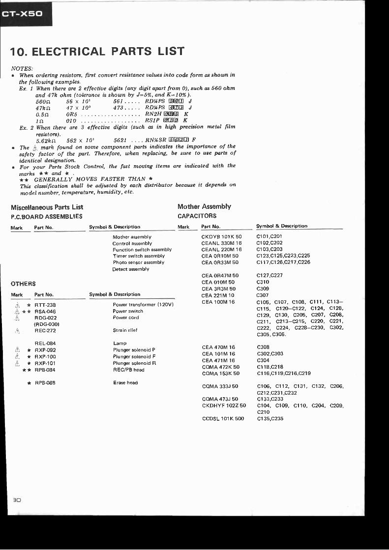
12.2.5
SettingModeTest TapeAC mV meterInput Signal
Recording/Playback FrequencyResponse Adjustment
Overall Frequency ResponseUsing STD-608A with DOLBY NR OFF
Using STD-603 with DOLBY NR OFE
Using STD-6OB with DOLBYNR ON
Using STD-604 with DOLBY NR OFF
63Hr 125H2 333H2 ,kHz Ê
Usîng STD-604 with DOLBYN.R ON
RecordSTD-608ALINE OUTPUT333H2, - 30dBv (31mV)to LINE INPUT
Procedure1. Set the TAPE SELECTOR to the NORM posi-
t ion.2. Adjust the INPUT level control so that the
AC mV meter reads - ZldBv (aa.6 mV).3. Record the 333H2 and 6.3kHz signals onto the
STD608A. Play back the tape and adjust theVR103 (L ch) and VR 203 (R ch) so that thedifference between two is OdB_t.b dB.
4. As listed in the specilications in Fig. 12-13and check to see that performance meetsspecifications.
Fig. 12-13 Recording/Playback frequency responseadjustment
Frequency ResponseUsing STD-331A with DOLBY NR OFFHoweuer, the right channel is compensated by -IdB at63H2, and -0.5d8 at 125H2 because of the ineulntioneffect.
63Hr r25Hr 333Hr e*", ea*",
Using STD-608A with DOLBY NR ON
V R 1 0 3 ( L c hVR203 (R cl '
333H2 ,kHz 6.3kHz lZtH.
63Hz t2sHz 333H2 zkHz 6,3kHr lgkHz
Fis. 12-14 Frequency responseFig. 12-15 Frequency response

12. nÉcLAGES12.1 nÉcleces mÉcarutouEsAvant de procéder au réglaç
Nettoyer les deux supports de bobine, le ca-bestan et le galet presseur à I'aide d'un bâtonnetimbibé d'alcool.
12.1.1 Réglaç de la force d'appui du galetpresseur
l. Mettre la platine en mode de reproduction.2. Appuyer doucement sur le bras du galet
presseur à I'aide d'une jauge de pression et sé-parer légèrement le galet presseur du cabestan.
3. Laisser ensuite revenir le galet presseur sur lecabestan et lire la valeur lorsque le galet pres-seur commence à toumer. Si la valeur lue nese situe pas entre 2O0g et 3509, remplacer leressort du galet presseur.
Cabestan
i"::::;tde Pression du
(Pièce no RBH-7601
Fig. 12-1 Réglage de la pression du galet-presseur
12.1.2 Réglage du couple du support de bobineMesurer le couple à I'aide d'un dynamomètre
dans les modes de lecture, d'avance rapide (FF) etde rebobinage (REW). Les valeurs mesurées doiventnormalement se situer dans les limites admissiblesdonnées au tableau 1.
Si les valeurs mesurées se trouvent en dehors desplages indiquées, remplacer I'assemblage support debobine TU (Éception) et/ou I'assemblage supportde bobine débiteur, la poulie libre TU ou I'assem-blage complet du bras d'entraînement.
Tableau I
12.1.3 Réglaç de la vitesse de défilement de labande
Raccorder le fréquencemètre aux bomes desortie LINE OUTPLTI.Reproduire la partie à SkHz de la bande d'essaiSTD-301. Au début, la fréquence doit se situerdans la plage de 2995H2 à 3010H2, et elle peutêtre réglée en toumant la Ésistance ajustablesituée dans le trou de réglage du moteur-cabestan, comme indiqué àlaîig. L2-2.
La vitese de défilement & la bande augmente lorsque la résis'ance ajustable est tournée dans le sens des aiguilles d'une montre.et elle d&roît lorsgue l'on tourna la résisânce cn sens inverse.
Vitsse de difilementde la bonde diminuée
Tournwis (-l
Fis.12-2 Réglage de la vitesse de défi lement de la bande
12.1.4 Réglage du contact de détection d'en-registrement
Régler I'ergot ( + ) indiqué par une flèchesur Ia Fig. 12-3 sur une position telle que si unecassette possédant une languette de protectioncontre I'effacement accidentel est chargée dans lelogement, le contact à levier soit enclenché (ON),et que si une cassette démunie de cette languettede protection est chargée, le contact soit déclenché(oFF).
Plaque latérale gauche
Levierde commutateur(Commutateurde détectiond'enregistrement)
Fig. 12-3 Réglage du commutateur de détectiond'enregistrement
1 .
2.
IIndicateur de tension(Pièce no GGKO4Tl
Bras du galet-presseur
Support debobine TU
Support debobine débitrice
Mode de reproduction 35 à 55g.cm o 2 à Sg.cmMode FF 75 à 110s.cm o 2 à Sg.cmMode REW o 2 à Sg.cm 75 à 11Og.cm
o Couple de tension inverse
40

12.2.6 Record Level AdjustmentSince this adjustment determinet thG DOLBY NR
leuel during reocrding, it should be performed preciæly.
SettingM o d e . . . . R e c o r dTest Tape . STD-608A, STD-608,
STD.604AC mV meter . . . Tpl (L ch) and Tpz
(R ch) of the motherassembly
I n p u t S i g n a l . . . . B g g H z , - 1 0 d B v ( B 1 6 m V )
rNpur lever conho, . . . 3ir"ÏNx INPUr
Procedure
1. Ctreck that the AC mV meter reads -b.2dBvt4dB (870mV - BbOmV ) and adjust the inputsignal level with attenuator so that the AC mVmeter reads :5.2dBv (0.iaV).
2. Next set ttre DOLBy NR switch to the ONposition.
3. Record the BBBHz signal onto the STD-60SA.eUy
!_1c!r-the tape and adjusr rhe V8102 (Lch)and- VR202 (Rch) so that the AC mV meteireads -5.2dBv (0.bV).
Record the 333H2 signal onto the STD-609.PIay back the tape and check that the ACmV meter reads -5.2dBv t1.5dB (650mV -460mV).Record the 333H2 signal onto the STD-604.Play back the tape and check that the AC mVmeter reads -5.2dBv t1.5dB (6b0mV -460mV).
ADJ.POINT
4 .
o .
12.2.6 Record levelADJ.
VR102 (Lch ) ,VR202 (Rchl
Fig. 12-16 Record level adjustment
TP2-p
g--vRrol
Q-vR203
@-VRt03
qI
vR202
Fig.12-t l ADJ. point
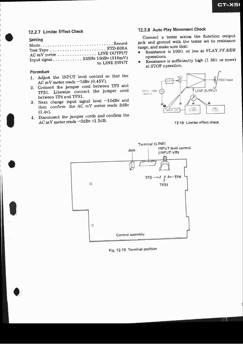
12.2.7 Limiter Effect Check
SettingMode Record
TestTape " ' STD-608A
AC mV meter ' LINE OUTPUT
Input signal . 333H2 10dBv (316mV)tO LINE INPUT
Porcedure1. Adjust the INPUT level control so that the
ACmV meter reads -?dBv (0'45V)'
2. Connect the jumper cord between TP3 and
TP31. Likewise connect the jumper cord
between TP4 and TP31'3. Next change input signal level -10dBv and
then confiim the AC mV meter reads SdBv
(1.4v).4. Disconnect the jumper cords and confirm the
AC mV meter reads -2dBv J1'5dB'
12.2.8 Auto PlaY Movement Check
Connect a tester actoss the function outputjack and ground with the tester set to resistance
range, and make sure that:;
"Resistance is 100o or less at PLAY'FF'REWoperations.
o Resistance is sufficiently high (1 Mo or more)
at STOP oPeration.
333H2 - | odBv( 3 r 6 m V )
12-18 Limiter effed check
I
Fig. 12-19 Terminal Position
LINE OUTPUT
Terminal (LINE)INPUT level control( INPUT VR}
TP3-_0 0 0-1P4
o rJsr

12.1.5 Réglage de l'assemblaç de déæctionDessener la vis O et régler la position de
montage de I'assemblage de détection de manièreà ce que lorsqu'une cassette de type "NORMAL"est chargée dans le logement le contact à curseursoit déclenché (OFF), et que lorsqu'une cassettede type "METAL" est chargée, le contact à curseursoit enclenché (ON).
Contact à curseur:--s
Ensemblede détection
Fig. 124 Réglage de l'assemblage de détection
12.1.6 Réglaç de ltlectreaimant d'avance rapide(FF I
Mettre la platine en mode d'avance rapide (FF).Dessener ta vis @ et régler la position demontage de l'électro-aimant d'avance rapide(FF) de manière à ce que le trou carré deI'assemblage support de bobine soit de niveauavec la bosse de I'assemblage du bras d'entraîne-ment (c'est-àdire avec un êcart zérol, commeindiqué sur la Fig. 12-5.
Système de base(ensemble du bras d'entrainement)
Séparation 0
Contre-cabestan
Support debobine
dérouleuse
Mode de rebobinaç(REW}
Contre{abestan
Support de bobine dérouleuse
Solénolde FF(avance rapidel
Position d'avancerapide (FF)
Séparation O
Support debobinedébitrice
Contrecabestan
lMod" d'"u"n""rapide (FF)
- Engrenage d'entrainement
Support de bobine dérouleuse
1 .2.
12.1.7 Réglaç(REW}
1. Mettre la(RE1V).
2. Dessener la vis G) et régler la position demontage de l'électro-aimant de rebobinage(REW) de manière à ce que le trou carré del'assemblage support de bobine soit de niveauavec la bosse de I'assemblage du bras d'enhaîne-ment (c'est-à-dire avec un êcart zéro\, commeindiqué sur la Fig. 12-5.
de l'électro-aimant de rebobinaç
platine en mode de rebobinageFig. 12-5 Réglage du solénoide FF (REW)
Engrenage

6.
12.2 REGLAGES ELECTRIOUES
Précautionsl. Les réglages mécaniques doivent être terminés.2. Nettoyer les pièces suivantes à I'aide d'un
bâtonnet imbibé d'alcool: tête d'enregistre-ment/reproduction, galet phesseur, tête d'effacement, counoies en caoutchuc et cabestan.
3. Démagnétiser la tête d'enregistrement/repro-duction à I'aide d'un démagnétiseur de tête.
4. Ne pas utiliser de toumevis magnétisé pour lesréglages.
5. tæs Églages et les mesures doivent être réaliséspour les canaux de gauche et de droite avec latension d'alimentation nominale.Les réglages doivent être effectués dans l'ordreindiqué dans ce manuel de service. Une modifi-cation de cet ordre peut empêcher la réalisationde réglages corrects et peut provoquer unebaisse de performance.Les niveaux en cours de mesure sont basés surOdBv = lV. Raccorder une charge fictive de50 kS} (47 à 52 kQ) entre les bornes de sortie(ouTPUT).Laisser chauffer (vieillissement) le CT-X50pendant quelques minutes avant de procéderaux réglages.Placer le commutateur DOLBY NR sur OFFsauf indication contraire.
Equ ipements/outils d'esai requis1. Bande d'essai
STD.331A
STD.341A
STD-608A
STD-603 Bande "CrO2" viergeSTD-604 Bande "METAL" viergeOscillateur BFMillivoltmètre altematif (mV CA)AtténuateurOscilloscopeRésistance 50 kS} (47 à 52 kA )
L€VEL ( dEI
3 3 f H rf33Hr I r4 rHr l l2 5 rH I o t H . 8r t r ; 3 r H
- 20
3O..c 3O..c lo3.c lO..c 603.. lo.ac 3O..c
Fig. 12€ Contenu de la bande d'essaiSTD-331ANiwau (dBl
12.2.1 Réglage du circuit DOLBY NR
PréparationMode . . . . EnregistrementMillivoltmètre CA. . . . . TPl (canal de gauche
('L") et TP2 (canal dedroit "R") de I'assem-blage principal
Signal d'entrée . . 2kHz, - LOdBv (316mV)à I'entrée de ligno LINEINPUT
Proédure1. Régler la commande de niveau d'entrée INPUT
de manière à ce que le millivoltmètre CAindique - 2,2dBv ( 776mV).
2. Faire ensuite passer le niveau du signal d'entréeà -30dBv (31,6mV) et placer le commutateurDOLBY NR sur la position ON.
3. Régler VR-304 de manière à ce que le milli-voltmètre CA indique - 17,9dBv (127mV).
Entée de I ine( L I N E I N P U T ) TêÉ
d'enregistrement
7 .
8.
9 .
2kHz, -lOdBv(316mV)2kHz, -30dBv(31,6mV1
/rpi(€nal de
gache "L")- -J {ceôa l
de droi t
I R } t
Pour le propos généralde la reproductionPour le réglage de lareproductionBande "NORMAL"vierge
FiS.128 Réglage du circuit Dolby NR
12.2.2 Réglage en azamut de la têtePréparationMode ReproductionBanded'essai . . . . STD-341A(10kHz,
- 20dB)Millivoltmètre CA Sortie de ligne
(LINE OUTPUT)VR101, VR201 . . Tournées en position
maxlmumProédure
Régler la vis de Églage d'azimut de manière àobtenir I'indication maximum du millivoltmètreCA pour les canaux de gauche et de droite.Lorsque ce réglage est terminé, verrouiller la vis àI'aide du blocage de vis.
l-r/r d" Gl"s" d'dffiil
n v -rête de lÈ-@l--\E1ti€
de rione (L|NE ourPur)
reproductionl- |,--/ l ?-1---.lI - | gsorololC@re1
J | | Y l m a x l m u m lsrD-341A I I l -1okHz. -2OdB â
2.3.4.ô.6.
o- ? o
Fig. 12-7 Contenu de la bande d'essai STD-341AFig. 12-9 Réglage d'azimut de la tête

I nEs ts l0Rs:ldbrd in A ZW !5S tol.ræ u.l6 olh.Mi* mrd k t9,
M : Mo, lF l ' l% lc l I ' 2$ {x , i rO. , t , !æ% rorÙ.æe
2 CAPACIIOFSlldÉùd h csiiY {!Fl/d(ç (Vt ùd6ot@U mtd o I gF
rdtdion whh@t rcnç i3 æv.!c@t êlærolYtb c+æior
3 VOLIAG€
E : æ É t ç l v ) . t É i F r t i F l
. O 'HEÂS:
A : eiuli4 æinrrh. /h m..r l@d d m mæ6r Ènr dt6 th. 'm
FilEa ol ft eey læto. ol rtu M. Tkçl@,ùrdæiq,h ræ burFnso l ûn tÈ. lddgn i l 'on
2SA826LN2SC1740LN
HAl200584843
-5 STTCHES
5I : PMR52,3 : P l^Y
52,5 reW
ON - OFFo -trFs - o fd -gEE
9,5: sloP oN - gfE
56 : PAUSE57 : FEC
$ . REC MUE
oN- f f i
O N - 6 F59 : OCBY NR q -gqEsro EN æwNrmcu HglE - @.!9!Esfi T|MER ON - 9fE5i2 : TIMER PLAY _.æqs r 3 : M S oN -otr
NOTE:Playbach signal route
-_-Recording signal routeSl4 rff i SEÉCTG W-C.O2
Sl5 : IPE SEÉCTæ ç!93 - GTAL
lhuùlid idic.G rhe *i ld æ.iton
Thk is th. bb æh6.i. diqrh br r6a æùd ci@n Êv v.ry
dù. ro inÈdmnc in 6iS.
I7
25A11272SC2634
HD7432
L o t N o
zSC2(b0
Typ. No
8A336
25D837 H411226HAt2006
2SD1031 M512o2L
lype No
NOTE:The indicated semiconductorc are repreæntatiue onesonly. Other alternative semiconductora may be used andare listed in the parts list.
L J
-

1O. ELECTRICAL PARTS LISTNOlES:o When ordertng resistorc, first convert resistance wlues into code form æ shown in
the following examples.Ex. 1 When there are 2 effectiue digits (any d.igit apart from 0), such æ 560 ohm
and 47h ohm (tolerance is shown by J=5%, and K=10% ).560f) 56 x 1014 7 h a 4 7 x 1 0 3
5 6 1 . . . . . R D % P S E B E J473. . . .. RD%PS EAPIB J
o . s a 0 R 5 . . . . . . n N 2 r l [ Ù E B Kr o 0 1 0 . . . . . . R S I P @ n @ K
Ex. 2 When there are 3 effectiue digits (such æ in high precision metal filmresistorc).5.62ko 562 x 10 ' 5621 . . . . RN'/SR EltrEE r
o The I marh found on some component parts indicates the importance of the
safeti factor of the part. Therefore, when replacing, be sure to use parts of
ide ntical designation,o For your Parts Stoch controt, the fast mouing items are indicated with the
marhs ** and *** GENERALLY MOVES FASTER THAN *
This ctasification shall be adiusted by each distributor becarse it depends on
model number, temperature, humidity, etc'
Misccllaneous Parts LastP.C.BOARD ASSEMBLIES
Mother AssemblyCAPACITORS
Mark Part No. Symbol & DescriptionMark Part No. Symbol & DescriPtion
OTHERS
Mark Part No.
Mother assembly
Control assemblYFunction switch assemblYTimer switch assemblYPhoto sensor assembly
Detect assemblY
Symbol & Description
CKDYB '01 K 50CEANL 33OM 16CEANL 22OM 16CEA ORlOM 50CEA OR33M 50
CEA OR47M 50cEA 010M 50CEA 3R3M 50cEA 221M 10cEA 100M 16
cEA 470M 16c E A 1 0 1 M 1 6c E A 4 7 1 M 1 6coMA 472K 50coMA 1 53K 50
coMA 333J 50
coMA 473J 50C K D H Y F 1 O 2 Z 5 0
ccDsL 101 K 500
cl01,c201c102,c202c103,c203c123,C125,C223,C225c117 ,C126,C217 ,C226
c127,C227c310c309c307c l05 , c l 07 , c l 08 , C l11 , C l13 -c115, C120-C122, C124, C12A,c129, C130. C205, C207, c208,c211. C213-c2J5, C220, c221,c222, C224, C228-C230, C302.c305. c306.
c308c302,c303c304cl 18,C218cl 16,C1 19,C216,C219
c106, c112, C131, C132, C206,c212,C231 ,C232c1 33,C233c104, cl09, cl10, c204, c209,c210c1 35,C235
i \ *A * *A
A
RTT.238R5A046RDG.O22{RDG{301REC-272
Power transformer (1 2OVlPower switchPower cord
Strain r l ie f
LampPlunger solenoid P
Plunger solenoid F
Plunger solenoid RREC/PB head
Erase head
AAL
BELO84* RXP-092* RXP-100r RXP-101
rr RPBO84
* RPBO8s

Mark Part No. Symbol & OescriPtion
RESISTORS
NOTE:When ordering resistors' conuert -the resistance ualue
into cod.e fo"*,'iii tn"i rewite the part no' as before'
Symbol & DescriPtion
cEA 330M 16
cEA 470M 16cEA221M 16cEA 102M 16cEA222r/l 16
cEA 471M 25
cÊA22'tM25coMA 102J 50
coMA 103J 50
coMA 104J 50
CKDYF 1032 50
C K D H Y F 1 O 2 Z 5 0CKDHYF 1 O3Z 50
CKDYF 473250
RCG-007
cr'.20c402,c4a3,C444c412,c437c439c416
c415c413c424c418,c/.21c422
c445c409c411c435
Part No.
SEMICONDUCTORS
t R c P l 1 5(RCP-2001
* RcP-150(RCP-195)
* BcP-149(RCP-193)RSl PF 56OJRD1 /4PM OOÛJ
VR103,VR2O3 Semi-f ixed 150k-B
VRlOl ,VR2O1 Semi-f ixed 22k'B
VR102,VFl202 Semi-tixed 10K-B
VR3Ol8304R101-Rl37 , R139-R145, R201-
R237, R239-R245, R301-R303'
R3o5-R307, Ft309, R310
Symbol & Description
rc101,1C2011c l02
01 o 1 -o1 07,0201 -a207'0301
Dl01 ,D201
D102,D202,D301-D306
2D30120302
c408 Capacitor array
Mark Part No.
* r HA12005** HA11226
RESISTORS
NOTE:When ordering resistors' cont)ert -the resistance value
into code fo'^, olii tn"i rewrite the part no' as before'
* * 2SC1 740LN(2SC263411 K34A(lK60A)toA90)ts2473
wz-o73w2-044
Part No.
Part No. Symbol & DescriPtion
a RCV-093
RSl /2PSF 561JR S l P F 1 3 1 J
RD1 /4PM trtrDJ
VR1-1 , VRl-2 Variable 2Ok-A
R455, R485R453
R4o1-R452, R454, R456-R484',
Fr486-R496I
I
colLsMark
SEMICONDUCTORSSymbol & DeTniPtion
Mark Part No. Symbol & Description
RTX-OIORTF-085RTF{84RTD-083
RSR.O35
Control AssemblYCAPACITORS
OSC btock
Peaking coi l {3 '9mH)
TraP coil
MPX f i l ter btock
Relay
* * HA12006** 8A843** 8A336** HD7432** M51202L
r* 2sc1740LN(2Sc26341
** 2SC2060** 25A1127
(25A826LN)
** 2SC1740LNl , ** zsotoat
(2SD837)
* 152473
r WO3B(wo3C)
* 1K344(1 K60A)
tc4011c4021c403tc404rc405
Q401, c,404-0406, 0409,
0414. Q417, 0419,
0407. 0408, 0410,0,4210402,0403,o418,0.420
a422-o,425o412
D4o1-D403, D4o7-D409, D41
D414, D41g'D429, D432,
D4o4-D406, D415
D416.D417,D430,D431
T301L1 03,L203L102,L202L l01 ,L210
RY3O1
Mark Part No' Symbol & Description
coMA 223K 50
CEA ORlOM 50
CEA OR22M 50
CEA OR33M 50
cEA 010M 50
cEA 470M 10
c E A 1 0 1 M 1 0
c E A 2 2 1 M 1 0
cEA 100M 16
cEA 220M 16
c401c423ç417c419c427, c428, c433, c434, c441',
c442,C443
c407 ,c410 ,c440 'c445c404 ,c405 ,c4 I 4 ,c426c406c425,C429,C430-c432c436
5 l

12.2.5
SettingModeTest TapeAC mV meterInput Signal
Recording/Playback FrequencyResponse Adjustment
Overall Frequency ResponseUsing STD-608A with DOLBY NR OFF
Using STD-603 with DOLBY NR OFE
Using STD-6OB with DOLBYNR ON
Using STD-604 with DOLBY NR OFF
63Hr 125H2 333H2 ,kHz Ê
Usîng STD-604 with DOLBYN.R ON
RecordSTD-608ALINE OUTPUT333H2, - 30dBv (31mV)to LINE INPUT
Procedure1. Set the TAPE SELECTOR to the NORM posi-
t ion.2. Adjust the INPUT level control so that the
AC mV meter reads - ZldBv (aa.6 mV).3. Record the 333H2 and 6.3kHz signals onto the
STD608A. Play back the tape and adjust theVR103 (L ch) and VR 203 (R ch) so that thedifference between two is OdB_t.b dB.
4. As listed in the specilications in Fig. 12-13and check to see that performance meetsspecifications.
Fig. 12-13 Recording/Playback frequency responseadjustment
Frequency ResponseUsing STD-331A with DOLBY NR OFFHoweuer, the right channel is compensated by -IdB at63H2, and -0.5d8 at 125H2 because of the ineulntioneffect.
63Hr r25Hr 333Hr e*", ea*",
Using STD-608A with DOLBY NR ON
V R 1 0 3 ( L c hVR203 (R cl '
333H2 ,kHz 6.3kHz lZtH.
63Hz t2sHz 333H2 zkHz 6,3kHr lgkHz
Fis. 12-14 Frequency responseFig. 12-15 Frequency response

12. nÉcLAGES12.1 nÉcleces mÉcarutouEsAvant de procéder au réglaç
Nettoyer les deux supports de bobine, le ca-bestan et le galet presseur à I'aide d'un bâtonnetimbibé d'alcool.
12.1.1 Réglaç de la force d'appui du galetpresseur
l. Mettre la platine en mode de reproduction.2. Appuyer doucement sur le bras du galet
presseur à I'aide d'une jauge de pression et sé-parer légèrement le galet presseur du cabestan.
3. Laisser ensuite revenir le galet presseur sur lecabestan et lire la valeur lorsque le galet pres-seur commence à toumer. Si la valeur lue nese situe pas entre 2O0g et 3509, remplacer leressort du galet presseur.
Cabestan
i"::::;tde Pression du
(Pièce no RBH-7601
Fig. 12-1 Réglage de la pression du galet-presseur
12.1.2 Réglage du couple du support de bobineMesurer le couple à I'aide d'un dynamomètre
dans les modes de lecture, d'avance rapide (FF) etde rebobinage (REW). Les valeurs mesurées doiventnormalement se situer dans les limites admissiblesdonnées au tableau 1.
Si les valeurs mesurées se trouvent en dehors desplages indiquées, remplacer I'assemblage support debobine TU (Éception) et/ou I'assemblage supportde bobine débiteur, la poulie libre TU ou I'assem-blage complet du bras d'entraînement.
Tableau I
12.1.3 Réglaç de la vitesse de défilement de labande
Raccorder le fréquencemètre aux bomes desortie LINE OUTPLTI.Reproduire la partie à SkHz de la bande d'essaiSTD-301. Au début, la fréquence doit se situerdans la plage de 2995H2 à 3010H2, et elle peutêtre réglée en toumant la Ésistance ajustablesituée dans le trou de réglage du moteur-cabestan, comme indiqué àlaîig. L2-2.
La vitese de défilement & la bande augmente lorsque la résis'ance ajustable est tournée dans le sens des aiguilles d'une montre.et elle d&roît lorsgue l'on tourna la résisânce cn sens inverse.
Vitsse de difilementde la bonde diminuée
Tournwis (-l
Fis.12-2 Réglage de la vitesse de défi lement de la bande
12.1.4 Réglage du contact de détection d'en-registrement
Régler I'ergot ( + ) indiqué par une flèchesur Ia Fig. 12-3 sur une position telle que si unecassette possédant une languette de protectioncontre I'effacement accidentel est chargée dans lelogement, le contact à levier soit enclenché (ON),et que si une cassette démunie de cette languettede protection est chargée, le contact soit déclenché(oFF).
Plaque latérale gauche
Levierde commutateur(Commutateurde détectiond'enregistrement)
Fig. 12-3 Réglage du commutateur de détectiond'enregistrement
1 .
2.
IIndicateur de tension(Pièce no GGKO4Tl
Bras du galet-presseur
Support debobine TU
Support debobine débitrice
Mode de reproduction 35 à 55g.cm o 2 à Sg.cmMode FF 75 à 110s.cm o 2 à Sg.cmMode REW o 2 à Sg.cm 75 à 11Og.cm
o Couple de tension inverse
40
12.2.6 Record Level AdjustmentSince this adjustment determinet thG DOLBY NR
leuel during reocrding, it should be performed preciæly.
SettingM o d e . . . . R e c o r dTest Tape . STD-608A, STD-608,
STD.604AC mV meter . . . Tpl (L ch) and Tpz
(R ch) of the motherassembly
I n p u t S i g n a l . . . . B g g H z , - 1 0 d B v ( B 1 6 m V )
rNpur lever conho, . . . 3ir"ÏNx INPUr
Procedure
1. Ctreck that the AC mV meter reads -b.2dBvt4dB (870mV - BbOmV ) and adjust the inputsignal level with attenuator so that the AC mVmeter reads :5.2dBv (0.iaV).
2. Next set ttre DOLBy NR switch to the ONposition.
3. Record the BBBHz signal onto the STD-60SA.eUy
!_1c!r-the tape and adjusr rhe V8102 (Lch)and- VR202 (Rch) so that the AC mV meteireads -5.2dBv (0.bV).
Record the 333H2 signal onto the STD-609.PIay back the tape and check that the ACmV meter reads -5.2dBv t1.5dB (650mV -460mV).Record the 333H2 signal onto the STD-604.Play back the tape and check that the AC mVmeter reads -5.2dBv t1.5dB (6b0mV -460mV).
ADJ.POINT
4 .
o .
12.2.6 Record levelADJ.
VR102 (Lch ) ,VR202 (Rchl
Fig. 12-16 Record level adjustment
TP2-p
g--vRrol
Q-vR203
@-VRt03
qI
vR202
Fig.12-t l ADJ. point

12.2.7 Limiter Effect Check
SettingMode Record
TestTape " ' STD-608A
AC mV meter ' LINE OUTPUT
Input signal . 333H2 10dBv (316mV)tO LINE INPUT
Porcedure1. Adjust the INPUT level control so that the
ACmV meter reads -?dBv (0'45V)'
2. Connect the jumper cord between TP3 and
TP31. Likewise connect the jumper cord
between TP4 and TP31'3. Next change input signal level -10dBv and
then confiim the AC mV meter reads SdBv
(1.4v).4. Disconnect the jumper cords and confirm the
AC mV meter reads -2dBv J1'5dB'
12.2.8 Auto PlaY Movement Check
Connect a tester actoss the function outputjack and ground with the tester set to resistance
range, and make sure that:;
"Resistance is 100o or less at PLAY'FF'REWoperations.
o Resistance is sufficiently high (1 Mo or more)
at STOP oPeration.
333H2 - | odBv( 3 r 6 m V )
12-18 Limiter effed check
I
Fig. 12-19 Terminal Position
LINE OUTPUT
Terminal (LINE)INPUT level control( INPUT VR}
TP3-_0 0 0-1P4
o rJsr

12.1.5 Réglage de l'assemblaç de déæctionDessener la vis O et régler la position de
montage de I'assemblage de détection de manièreà ce que lorsqu'une cassette de type "NORMAL"est chargée dans le logement le contact à curseursoit déclenché (OFF), et que lorsqu'une cassettede type "METAL" est chargée, le contact à curseursoit enclenché (ON).
Contact à curseur:--s
Ensemblede détection
Fig. 124 Réglage de l'assemblage de détection
12.1.6 Réglaç de ltlectreaimant d'avance rapide(FF I
Mettre la platine en mode d'avance rapide (FF).Dessener ta vis @ et régler la position demontage de l'électro-aimant d'avance rapide(FF) de manière à ce que le trou carré deI'assemblage support de bobine soit de niveauavec la bosse de I'assemblage du bras d'entraîne-ment (c'est-àdire avec un êcart zérol, commeindiqué sur la Fig. 12-5.
Système de base(ensemble du bras d'entrainement)
Séparation 0
Contre-cabestan
Support debobine
dérouleuse
Mode de rebobinaç(REW}
Contre{abestan
Support de bobine dérouleuse
Solénolde FF(avance rapidel
Position d'avancerapide (FF)
Séparation O
Support debobinedébitrice
Contrecabestan
lMod" d'"u"n""rapide (FF)
- Engrenage d'entrainement
Support de bobine dérouleuse
1 .2.
12.1.7 Réglaç(REW}
1. Mettre la(RE1V).
2. Dessener la vis G) et régler la position demontage de l'électro-aimant de rebobinage(REW) de manière à ce que le trou carré del'assemblage support de bobine soit de niveauavec la bosse de I'assemblage du bras d'enhaîne-ment (c'est-à-dire avec un êcart zéro\, commeindiqué sur la Fig. 12-5.
de l'électro-aimant de rebobinaç
platine en mode de rebobinageFig. 12-5 Réglage du solénoide FF (REW)
Engrenage

6.
12.2 REGLAGES ELECTRIOUES
Précautionsl. Les réglages mécaniques doivent être terminés.2. Nettoyer les pièces suivantes à I'aide d'un
bâtonnet imbibé d'alcool: tête d'enregistre-ment/reproduction, galet phesseur, tête d'effacement, counoies en caoutchuc et cabestan.
3. Démagnétiser la tête d'enregistrement/repro-duction à I'aide d'un démagnétiseur de tête.
4. Ne pas utiliser de toumevis magnétisé pour lesréglages.
5. tæs Églages et les mesures doivent être réaliséspour les canaux de gauche et de droite avec latension d'alimentation nominale.Les réglages doivent être effectués dans l'ordreindiqué dans ce manuel de service. Une modifi-cation de cet ordre peut empêcher la réalisationde réglages corrects et peut provoquer unebaisse de performance.Les niveaux en cours de mesure sont basés surOdBv = lV. Raccorder une charge fictive de50 kS} (47 à 52 kQ) entre les bornes de sortie(ouTPUT).Laisser chauffer (vieillissement) le CT-X50pendant quelques minutes avant de procéderaux réglages.Placer le commutateur DOLBY NR sur OFFsauf indication contraire.
Equ ipements/outils d'esai requis1. Bande d'essai
STD.331A
STD.341A
STD-608A
STD-603 Bande "CrO2" viergeSTD-604 Bande "METAL" viergeOscillateur BFMillivoltmètre altematif (mV CA)AtténuateurOscilloscopeRésistance 50 kS} (47 à 52 kA )
L€VEL ( dEI
3 3 f H rf33Hr I r4 rHr l l2 5 rH I o t H . 8r t r ; 3 r H
- 20
3O..c 3O..c lo3.c lO..c 603.. lo.ac 3O..c
Fig. 12€ Contenu de la bande d'essaiSTD-331ANiwau (dBl
12.2.1 Réglage du circuit DOLBY NR
PréparationMode . . . . EnregistrementMillivoltmètre CA. . . . . TPl (canal de gauche
('L") et TP2 (canal dedroit "R") de I'assem-blage principal
Signal d'entrée . . 2kHz, - LOdBv (316mV)à I'entrée de ligno LINEINPUT
Proédure1. Régler la commande de niveau d'entrée INPUT
de manière à ce que le millivoltmètre CAindique - 2,2dBv ( 776mV).
2. Faire ensuite passer le niveau du signal d'entréeà -30dBv (31,6mV) et placer le commutateurDOLBY NR sur la position ON.
3. Régler VR-304 de manière à ce que le milli-voltmètre CA indique - 17,9dBv (127mV).
Entée de I ine( L I N E I N P U T ) TêÉ
d'enregistrement
7 .
8.
9 .
2kHz, -lOdBv(316mV)2kHz, -30dBv(31,6mV1
/rpi(€nal de
gache "L")- -J {ceôa l
de droi t
I R } t
Pour le propos généralde la reproductionPour le réglage de lareproductionBande "NORMAL"vierge
FiS.128 Réglage du circuit Dolby NR
12.2.2 Réglage en azamut de la têtePréparationMode ReproductionBanded'essai . . . . STD-341A(10kHz,
- 20dB)Millivoltmètre CA Sortie de ligne
(LINE OUTPUT)VR101, VR201 . . Tournées en position
maxlmumProédure
Régler la vis de Églage d'azimut de manière àobtenir I'indication maximum du millivoltmètreCA pour les canaux de gauche et de droite.Lorsque ce réglage est terminé, verrouiller la vis àI'aide du blocage de vis.
l-r/r d" Gl"s" d'dffiil
n v -rête de lÈ-@l--\E1ti€
de rione (L|NE ourPur)
reproductionl- |,--/ l ?-1---.lI - | gsorololC@re1
J | | Y l m a x l m u m lsrD-341A I I l -1okHz. -2OdB â
2.3.4.ô.6.
o- ? o
Fig. 12-7 Contenu de la bande d'essai STD-341AFig. 12-9 Réglage d'azimut de la tête

L86
oC ( e I L - x ^ ^ 9 ) ^
o N l o - l
o
/v/eo9zcsz
c899tCdr'
M99I tVH
89tvsz
o N a d I I
v9ù6CSZvtezvsz
MOOSo3HCl_r i sNn
I
-r69''9W
to3zul8EI IVH
v-r00evd
9e9JSZrgrcsz
088(]S2erecsz
9Z.9ZCSZsgzLVSZ
ù-
VÂ . s s y
uo l vN t l i l ucs tos3l pue srolsrsuejl lo firuPjeaddy ;eura1x3
LI6