Creating a New TEL: Key Initiatives€¦ · · 2018-01-04Creating a New TEL: Key Initiatives...
42
Creating a New TEL: Key Initiatives Representative Director, President & CEO July 10, 2015 Tetsuro Higashi
Transcript of Creating a New TEL: Key Initiatives€¦ · · 2018-01-04Creating a New TEL: Key Initiatives...
Creating a New TEL: Key Initiatives
Representative Director, President & CEOJuly 10, 2015
Tetsuro Higashi
Corp IR/July 10, 2015
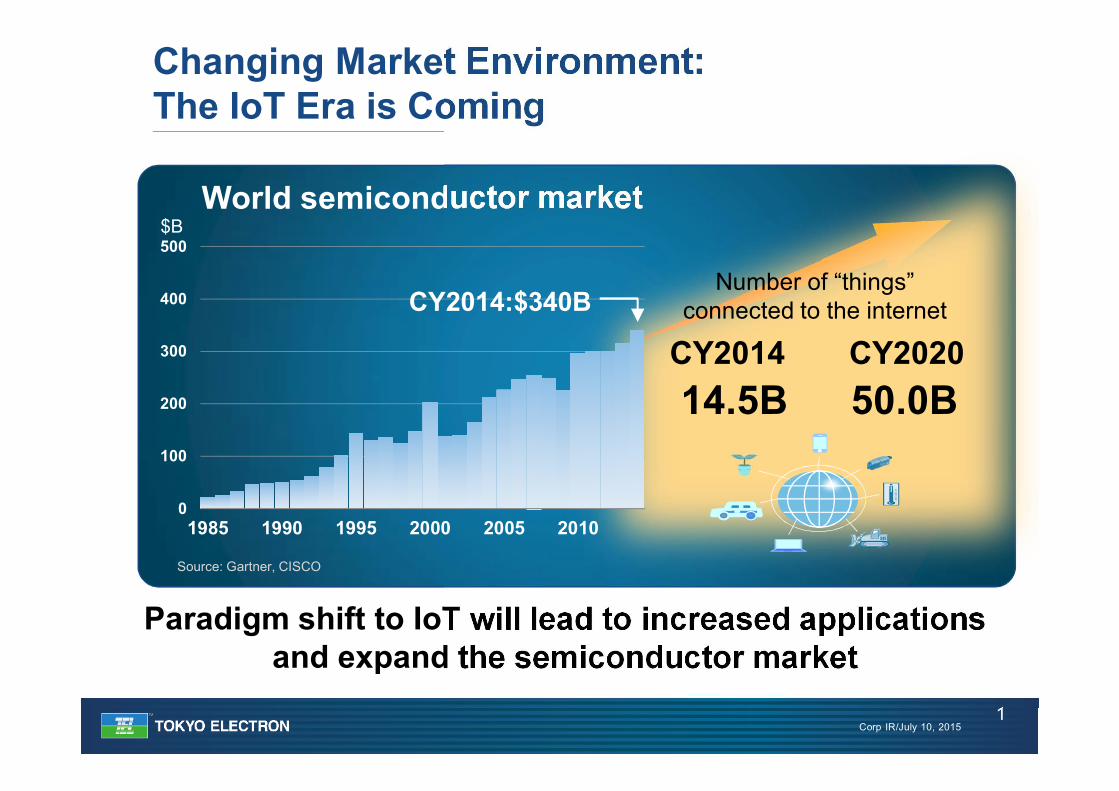
Changing Market Environment: The IoT Era is Coming
1
Paradigm shift to IoT will lead to increased applications and expand the semiconductor market
$BWorld semiconductor market
0
100
200
300
400
500
1985 1990 1995 2000 2005 2010
CY2014:$340BNumber of “things”
connected to the internet
CY2014 CY202014.5B 50.0B
Source: Gartner, CISCO

Corp IR/July 10, 2015
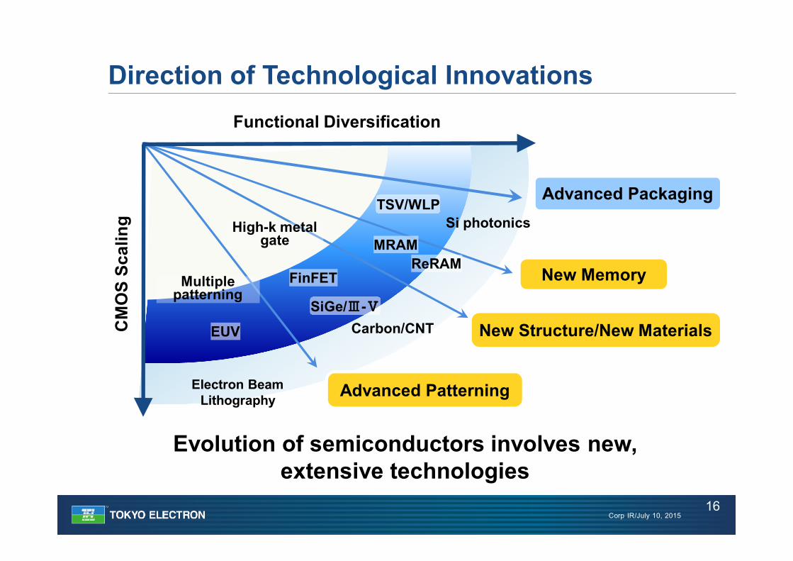
Functional DiversificationC
MO
S Sc
alin
g Si photonics
ReRAMMRAM
EUV
Multiple patterning
Carbon/CNT
Advanced Patterning
New Structure/New Materials
New Memory
Advanced Packaging
High-k metal gate
FinFET
TSV/WLP
Electron Beam Lithography
SiGe/Ⅲ-Ⅴ
Evolution of semiconductors involves new, extensive technologies
Direction of Technological Innovations
2
Corp IR/July 10, 2015
A real global company generating high added-value and profitsto Semiconductor and FPD
industries through innovative technologies and groundbreaking solutions with integrated diverse
technologies
Vision
3
Corp IR/July 10, 2015
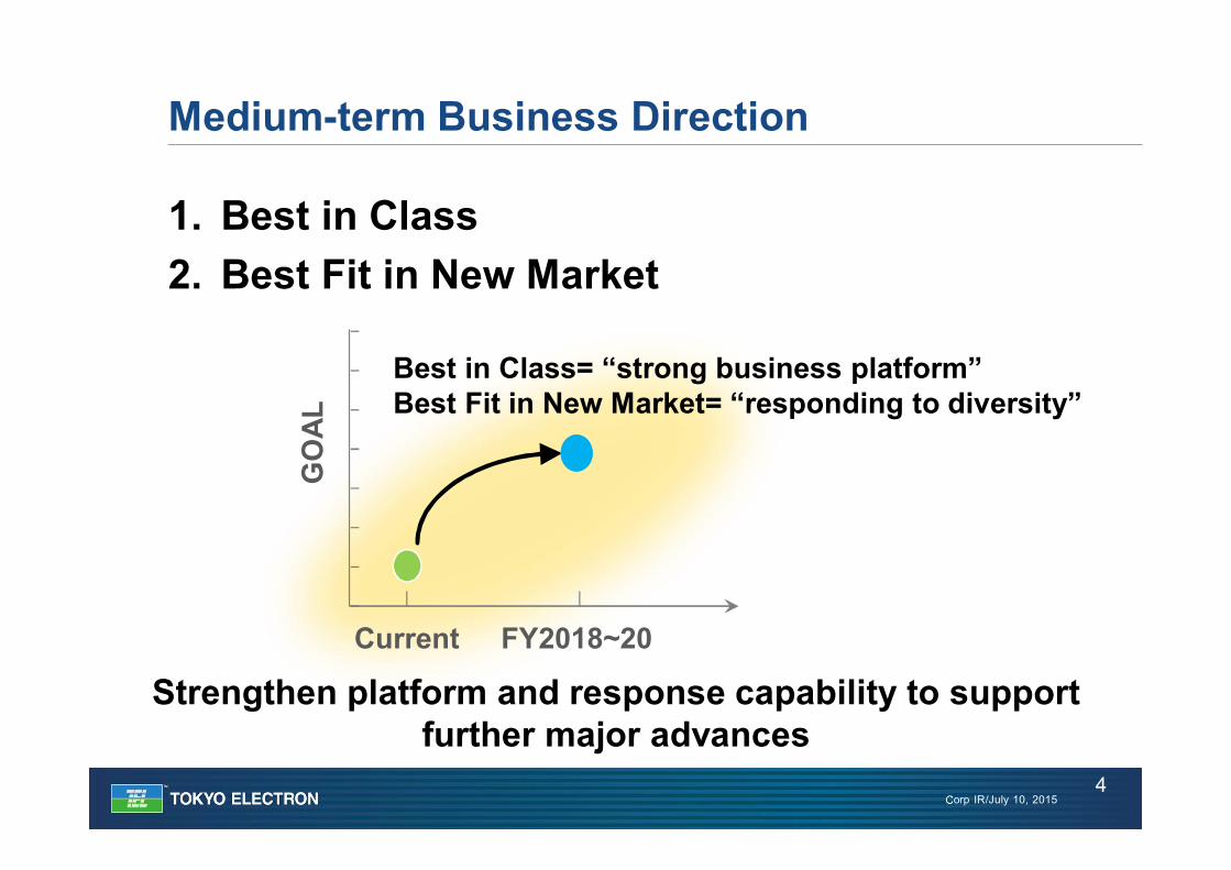
1. Best in Class2. Best Fit in New Market
Medium-term Business Direction
4
GO
AL
Best in Class= “strong business platform”Best Fit in New Market= “responding to diversity”
Current FY2018~20
Strengthen platform and response capability to support further major advances
Corp IR/July 10, 2015
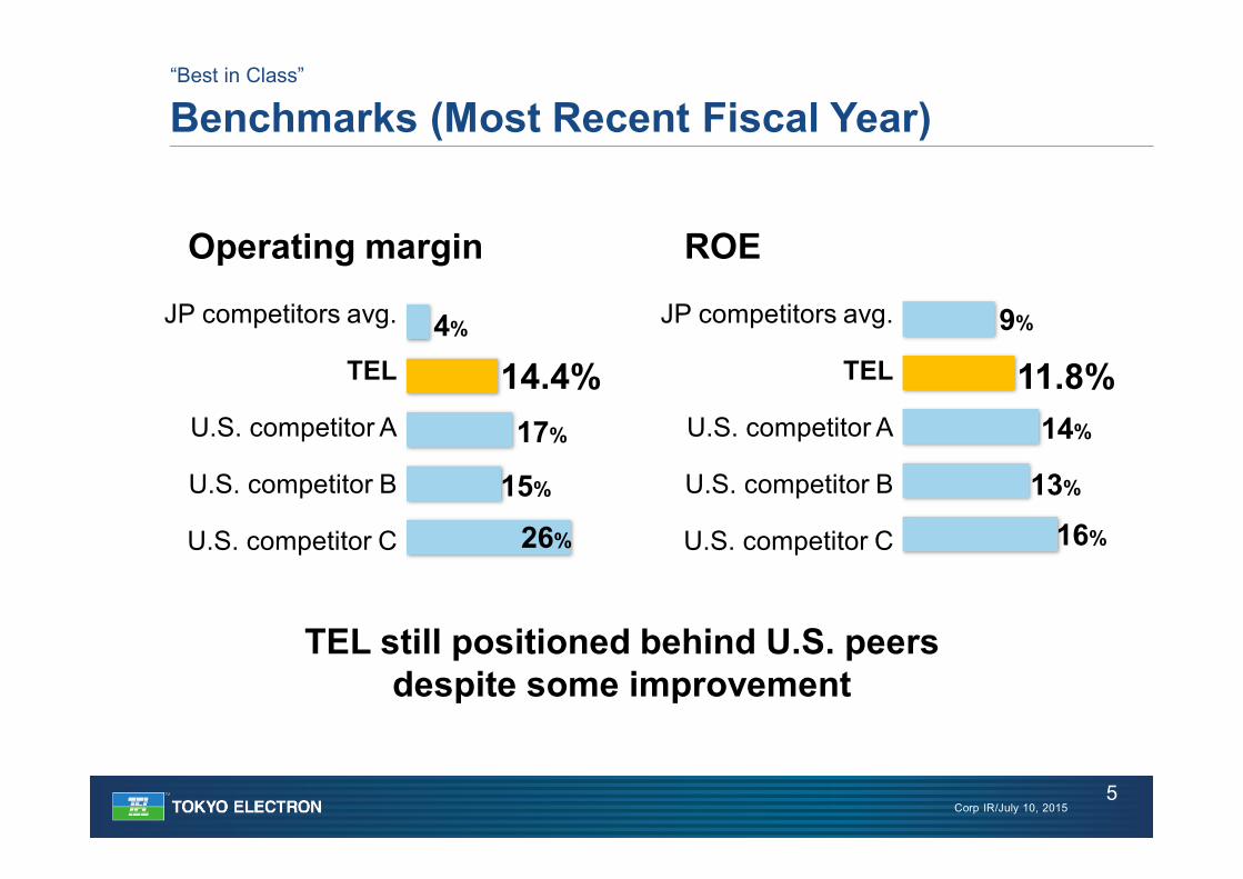
TEL still positioned behind U.S. peers despite some improvement
Benchmarks (Most Recent Fiscal Year)
5
ROE
16%
13%
14%
11.8%9%JP competitors avg.
TEL
U.S. competitor A
U.S. competitor B
U.S. competitor C
“Best in Class”
Operating margin
26%
15%
17%
14.4%4%JP competitors avg.
TEL
U.S. competitor A
U.S. competitor B
U.S. competitor C
Corp IR/July 10, 2015
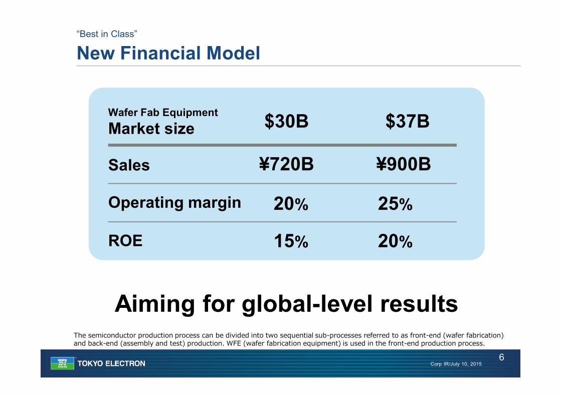
New Financial Model
6
Aiming for global-level results
$30B $37BWafer Fab EquipmentMarket size
Operating margin
ROE
20% 25%
15% 20%
Sales ¥720B ¥900B
“Best in Class”
The semiconductor production process can be divided into two sequential sub-processes referred to as front-end (wafer fabrication) and back-end (assembly and test) production. WFE (wafer fabrication equipment) is used in the front-end production process.
Corp IR/July 10, 2015
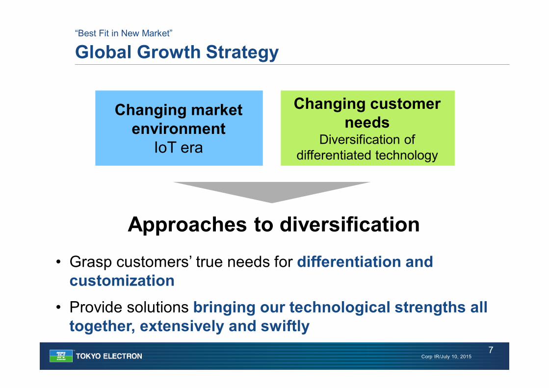
Changing customer needs
Diversification of differentiated technology
Changing market environment
IoT era
Global Growth Strategy
7
Approaches to diversification• Grasp customers’ true needs for differentiation and
customization• Provide solutions bringing our technological strengths all
together, extensively and swiftly
“Best Fit in New Market”

Corp IR/July 10, 2015
Fully utilize TEL’s corporate DNA―our track record of creating strong relationships of mutual trust, and work closely with
customers to overcome tough technological challenges
TEL
Customer
Supplier/Materials manufacturers
Global Growth Strategy
8
“Best Fit in New Market”
Corp IR/July 10, 2015
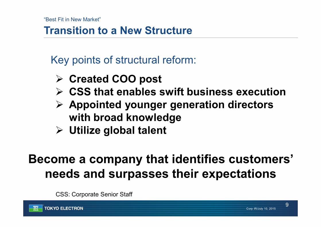
Transition to a New Structure
9
Key points of structural reform:
Created COO post CSS that enables swift business execution Appointed younger generation directors
with broad knowledge Utilize global talent
Become a company that identifies customers’ needs and surpasses their expectations
CSS: Corporate Senior Staff
“Best Fit in New Market”
Corp IR/July 10, 2015
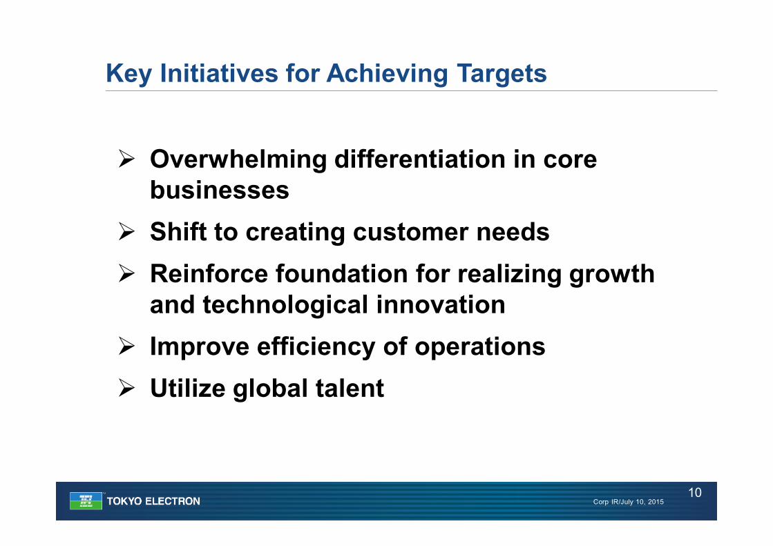
Key Initiatives for Achieving Targets
10
Overwhelming differentiation in core businesses
Shift to creating customer needs Reinforce foundation for realizing growth
and technological innovation Improve efficiency of operations Utilize global talent
Corp IR/July 10, 2015
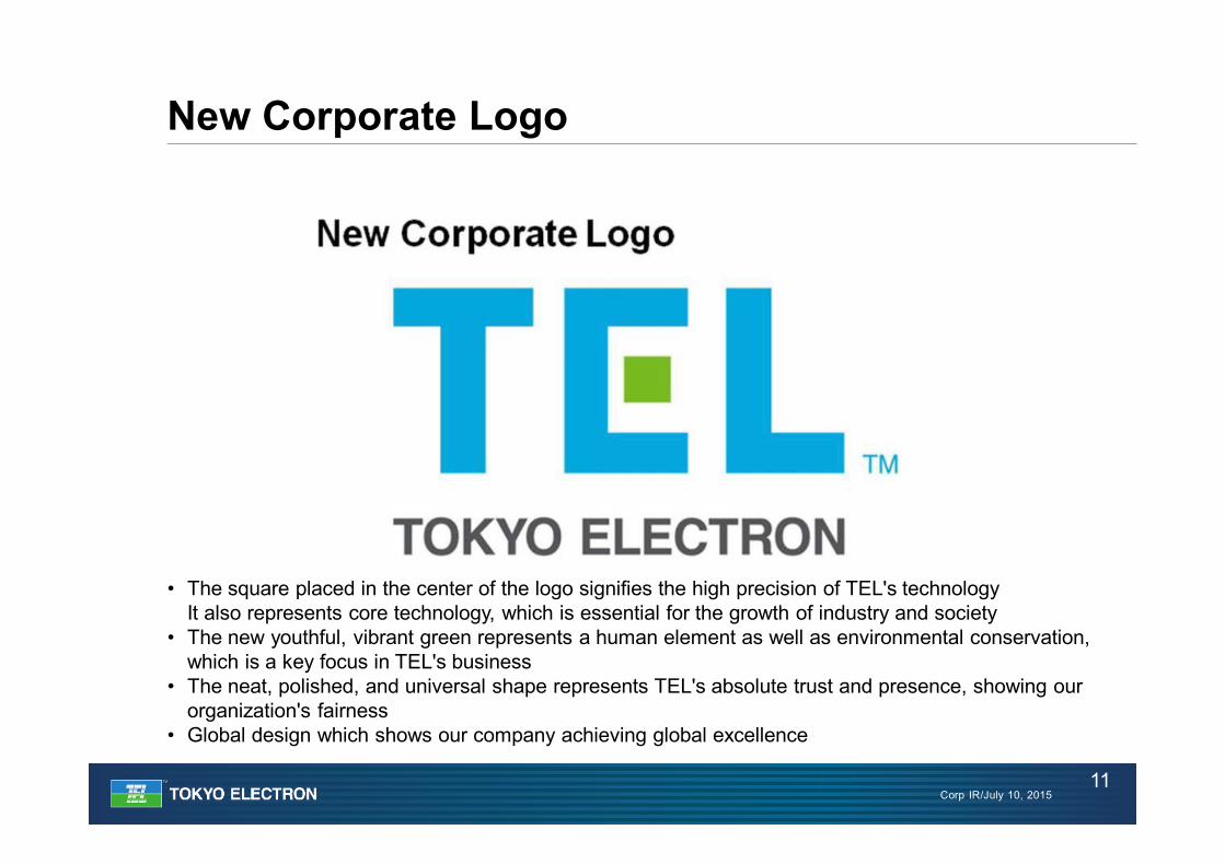
New Corporate Logo
11
• The square placed in the center of the logo signifies the high precision of TEL's technologyIt also represents core technology, which is essential for the growth of industry and society
• The new youthful, vibrant green represents a human element as well as environmental conservation, which is a key focus in TEL's business
• The neat, polished, and universal shape represents TEL's absolute trust and presence, showing our organization's fairness
• Global design which shows our company achieving global excellence

Medium-term Management Plan
Toshiki KawaiRepresentative Director, Senior Executive Vice President & COOJuly 10, 2015
Corp IR/July 10, 2015
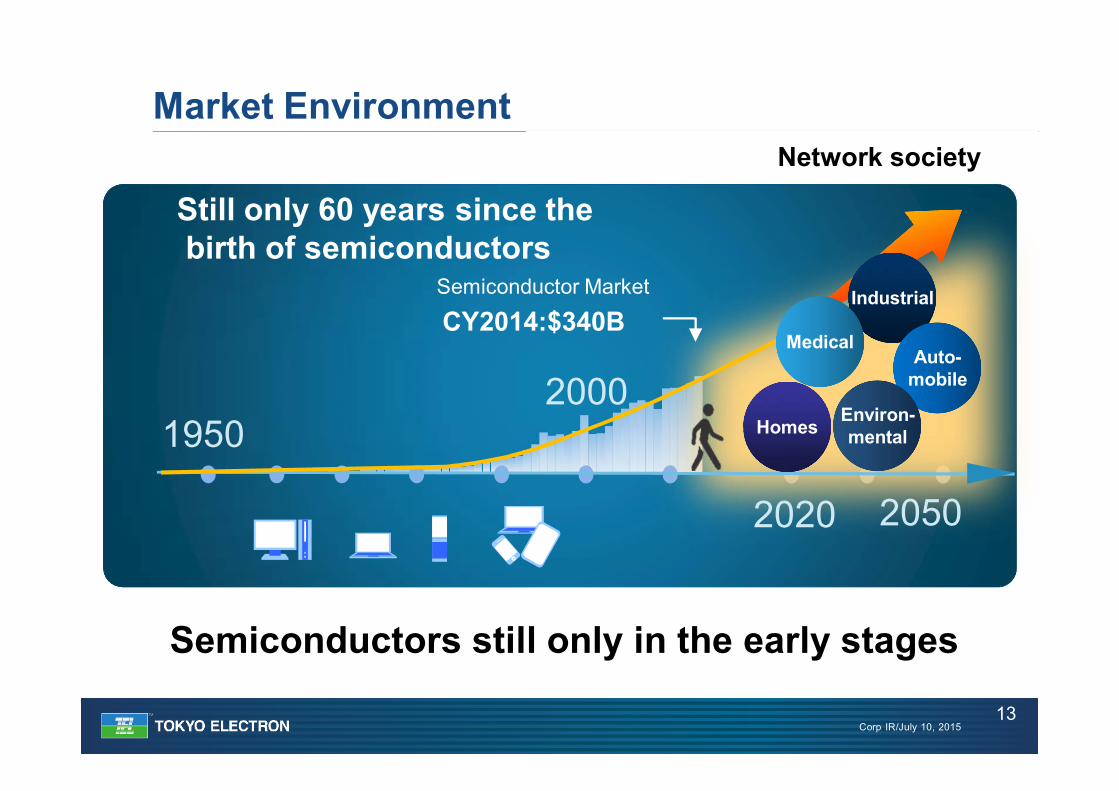
Semiconductors still only in the early stages
Market Environment
13
19502000
Network society
20502020
Still only 60 years since thebirth of semiconductors
Industrial
Auto-mobile
Environ-mentalHomes
CY2014:$340BSemiconductor Market
Medical
Corp IR/July 10, 2015
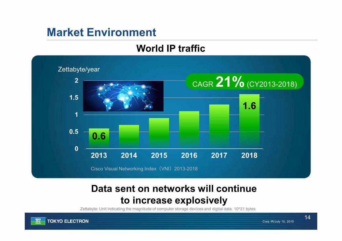
Market Environment
14
World IP traffic
0.6
1.6
0
0.5
1
1.5
2
2013 2014 2015 2016 2017 2018Cisco Visual Networking Index(VNI)2013-2018
CAGR 21% (CY2013-2018)
Zettabyte/year
Data sent on networks will continue to increase explosively
Zettabyte: Unit indicating the magnitude of computer storage devices and digital data. 10^21 bytes
Corp IR/July 10, 2015
Semiconductor Industry at an Inflection Point
10-7
10-5
10-4
DNA
10-3 m = 1mm
10-6 m = 1µm
10-8
10-10
10-12 m = 1pm10-11
1970
2010
1990
Blood Cell
Atom
Interatomic distance of Si
≒0.3nm
<10μm ~ 1nm>
Size range of LSI manufacturing
Inflection Point
Functional Diversification
CMOS Scaling
10-9 m = <10nm
15
Corp IR/July 10, 2015
Functional DiversificationC
MO
S Sc
alin
g Si photonics
ReRAMMRAM
EUV
Multiple patterning
Carbon/CNT
Advanced Patterning
New Structure/New Materials
New Memory
Advanced Packaging
High-k metal gate
FinFET
TSV/WLP
Electron Beam Lithography
SiGe/Ⅲ-Ⅴ
Evolution of semiconductors involves new, extensive technologies
Direction of Technological Innovations
16
Corp IR/July 10, 2015
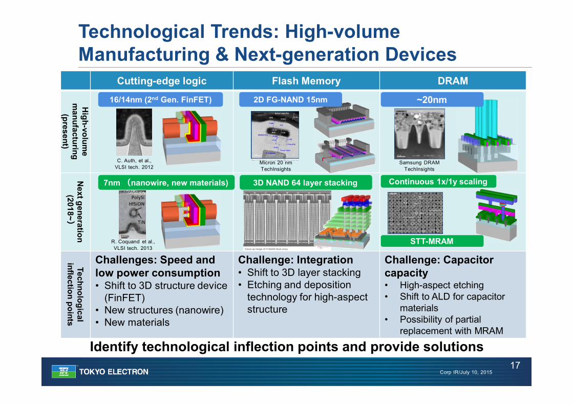
Technological Trends: High-volume Manufacturing & Next-generation Devices
17
Cutting-edge logic Flash Memory DRAM
High-volum
e m
anufacturing(present)
Next generation
(2018~)Technological
inflection points
Challenges: Speed and low power consumption• Shift to 3D structure device
(FinFET)• New structures (nanowire)• New materials
Challenge: Integration• Shift to 3D layer stacking• Etching and deposition
technology for high-aspect structure
Challenge: Capacitor capacity• High-aspect etching• Shift to ALD for capacitor
materials• Possibility of partial
replacement with MRAM
C. Auth, et al.,VLSI tech. 2012
16/14nm (2nd Gen. FinFET)
7nm (nanowire, new materials)
R. Coquand et al.,VLSI tech. 2013
2D FG-NAND 15nm
3D NAND 64 layer stacking
Micron 20 nmTechInsights
Samsung DRAMTechInsights
~20nm
Continuous 1x/1y scaling
STT-MRAM
Identify technological inflection points and provide solutions

Corp IR/July 10, 2015
Single wafer deposition
Wafer prober
CleaningCoater/developer
Etch
TEL product market share (CY2014)
Overwhelmingcompetitiveness
Thermal processing
Source: Gartner
TEL
Our SPE Competitiveness
18
Corp IR/July 10, 2015
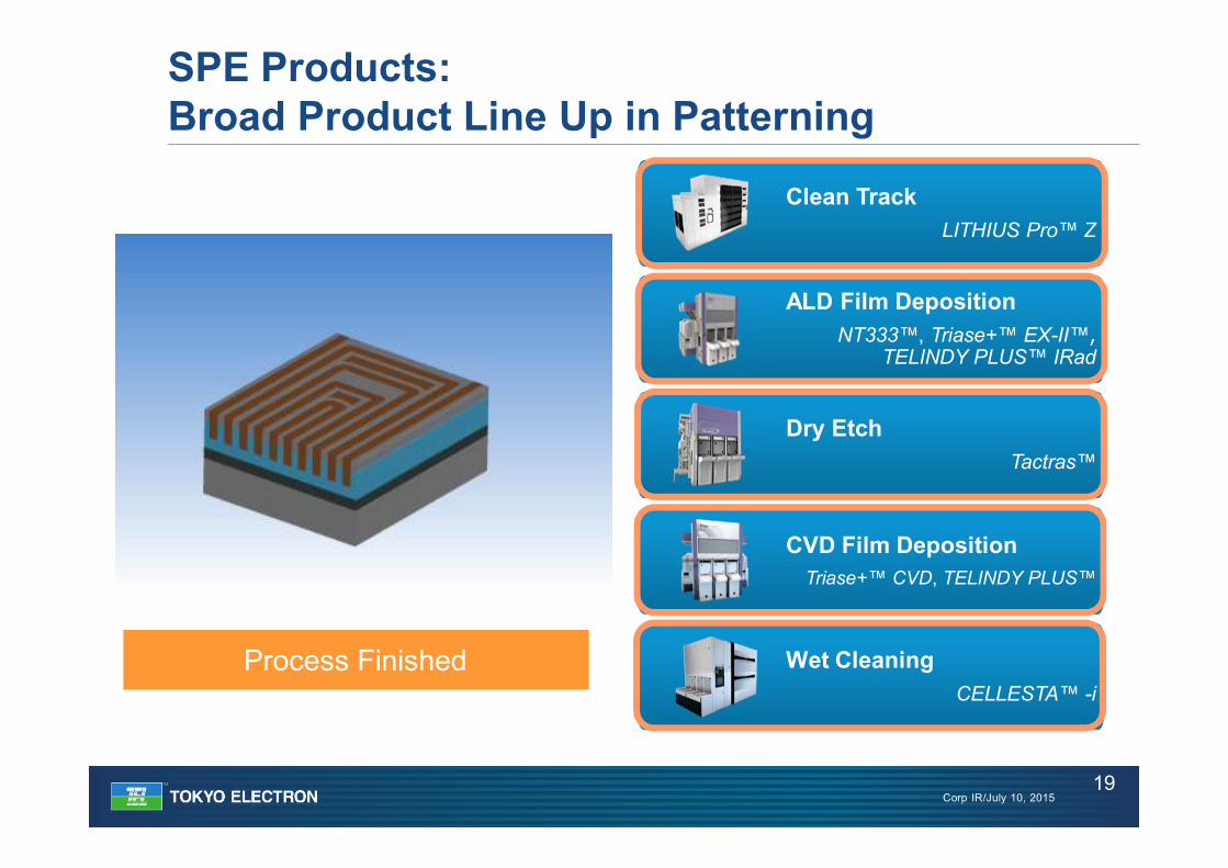
SPE Products: Broad Product Line Up in Patterning
19
Clean TrackLITHIUS Pro™ Z
ALD Film DepositionNT333™, Triase+™ EX-II™,
TELINDY PLUS™ IRad
Dry EtchTactras™
CVD Film DepositionTriase+™ CVD, TELINDY PLUS™
Wet CleaningCELLESTA™ -i
Wet CleaningWet CleaningULK DepositionUnder Layer 1 DepositionUnder Layer 2 DepositionMandrel DepositionUnder Layer 3 DepositionUnder Layer 3 DepositionWet CleaningWet CleaningBARC CoatingPR CoatingExposureExposurePR Trim EtchBARC Open EtchUnder Layer 3 Open EtchMandrel Open EtchMandrel Open EtchSpacer DepositionSpacer DepositionSOC CoatingSOC Trim BackSOC Trim BackSpacer Open EtchUnder Layer 2 Open EtchSOC RemovalUnder Layer 1 OpenUnder Layer 1 OpenUnder Layer 2 RemovalUnder Layer 2 RemovalMetal DepositionMetal DepositionPlanarizationProcess Finished
Corp IR/July 10, 2015
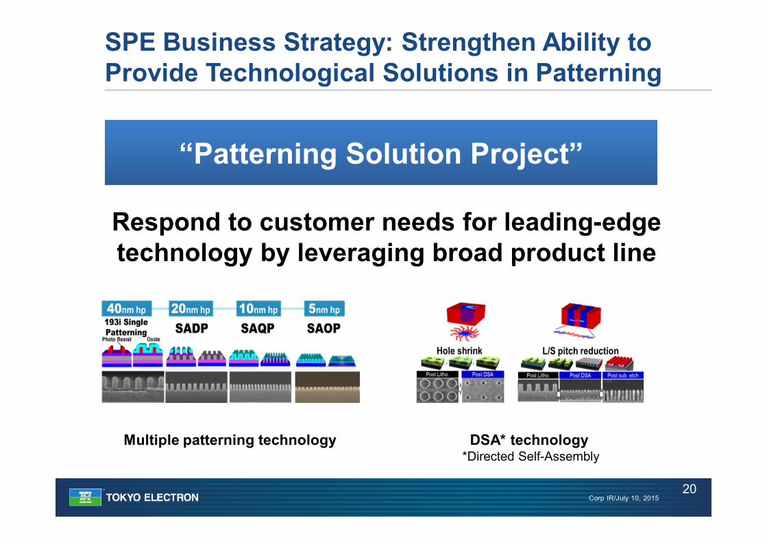
SPE Business Strategy: Strengthen Ability to Provide Technological Solutions in Patterning
20
Respond to customer needs for leading-edge technology by leveraging broad product line
“Patterning Solution Project”“Patterning Solution Project”
Multiple patterning technology DSA* technology*Directed Self-Assembly
Corp IR/July 10, 2015
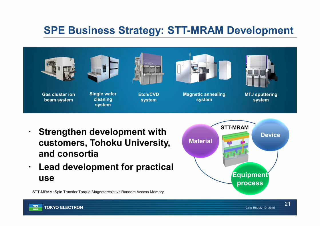
STT-MRAM: Spin Transfer Torque-Magnetoresistive Random Access Memory
SPE Business Strategy: STT-MRAM Development
21
Equipmentprocess
DeviceMaterial
Strengthen development with customers, Tohoku University, and consortia
Lead development for practical use
STT-MRAM
Gas cluster ion beam system
Magnetic annealing system
Etch/CVD system
Single wafer cleaning system
MTJ sputtering system

Corp IR/July 10, 2015
19%26%
CY2013 2014 ・・・ 2019
• Highest ever market share in 2014• Customer penetration in leading-edge
HVM lines progressing as planned, with our proprietary technology
• Expand applications of single wafer cleaning and dry cleaning system and further increase market share
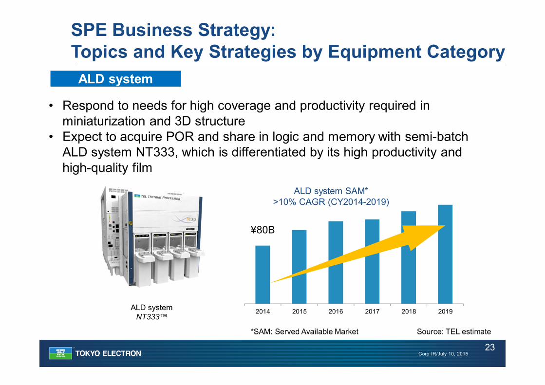
SPE Business Strategy: Topics and Key Strategies by Equipment Category
22
Cleaning systemCleaning system
Etching systemEtching system
Plasma Etch SystemTactras™
• Doubled sales in 2014 YoY and increased market share
• Acquire POR in patterning and memory HARC processes, where growth expected
TELshare
19%25%
CY2013 2014 ・・・ 2019
TELshare
Single WaferCleaning SystemCELLESTA™-i
Source:Gartner (market share in 2013 and 2014) and TEL estimate
POR (Process of Record):Certification of equipment application in customer semiconductor manufacturing processHARC: High Aspect Ratio Contact
Corp IR/July 10, 2015
2014 2015 2016 2017 2018 2019
• Respond to needs for high coverage and productivity required in miniaturization and 3D structure
• Expect to acquire POR and share in logic and memory with semi-batch ALD system NT333, which is differentiated by its high productivity and high-quality film
SPE Business Strategy: Topics and Key Strategies by Equipment Category
23
ALD systemALD system
ALD systemNT333™
ALD system SAM*>10% CAGR (CY2014-2019)
*SAM: Served Available Market Source: TEL estimate
¥80B
Corp IR/July 10, 2015
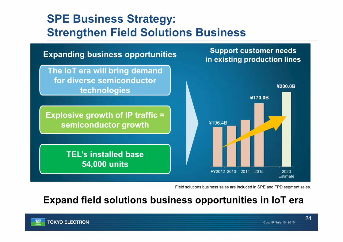
SPE Business Strategy: Strengthen Field Solutions Business
24
Field solutions business sales are included in SPE and FPD segment sales.
Expanding business opportunities
FY2012 2013 2014 2015 2020Estimate
Explosive growth of IP traffic = semiconductor growth
The IoT era will bring demand for diverse semiconductor
technologies
TEL’s installed base 54,000 units
¥170.0B
¥200.0B
Support customer needs in existing production lines
Expand field solutions business opportunities in IoT era
¥106.4B
Corp IR/July 10, 2015
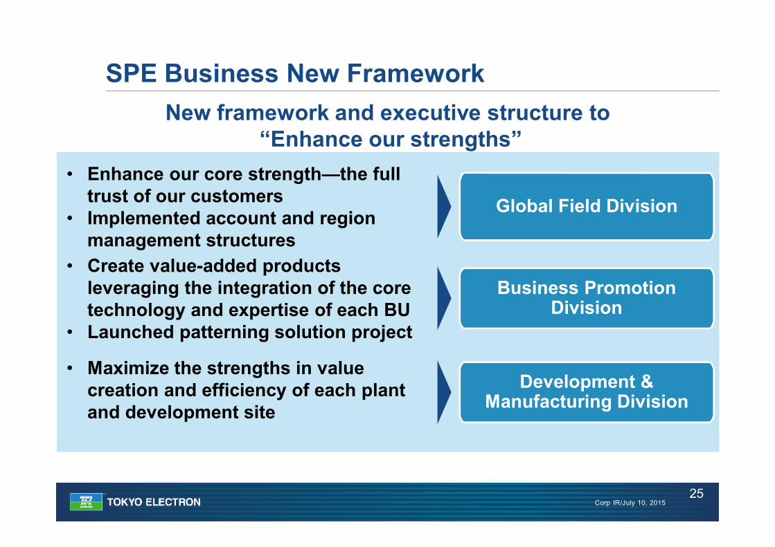
New framework and executive structure to“Enhance our strengths”
SPE Business New Framework
25
Business Promotion Division
Global Field Division• Enhance our core strength—the full
trust of our customers• Implemented account and region
management structures• Create value-added products
leveraging the integration of the core technology and expertise of each BU
• Launched patterning solution project
Development & Manufacturing Division
• Maximize the strengths in value creation and efficiency of each plant and development site
Corp IR/July 10, 2015
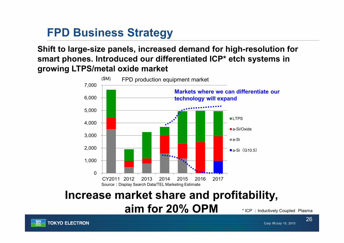
0
1,000
2,000
3,000
4,000
5,000
6,000
7,000
CY2011 2012 2013 2014 2015 2016 2017
LTPS
a-Si/Oxide
a-Si
a-Si(G10.5)
Shift to large-size panels, increased demand for high-resolution for smart phones. Introduced our differentiated ICP* etch systems in growing LTPS/metal oxide market
FPD Business Strategy
26* ICP :Inductively Coupled Plasma
FPD production equipment market($M)
Source:Display Search Data/TEL Marketing Estimate
Increase market share and profitability, aim for 20% OPM
Markets where we can differentiate our technology will expand
Corp IR/July 10, 2015
Toward profitability and ROE improvementFocus on SPE businessLeverage product line up and respond to
diversifying needsNew framework and executive structure to
enhance our strengths
Summary
27
Financial Model, Shareholder Returns Policy
Tetsuro HoriCorporate Director, Senior Vice President & General ManagerJuly 10 , 2015
Corp IR/July 10, 2015
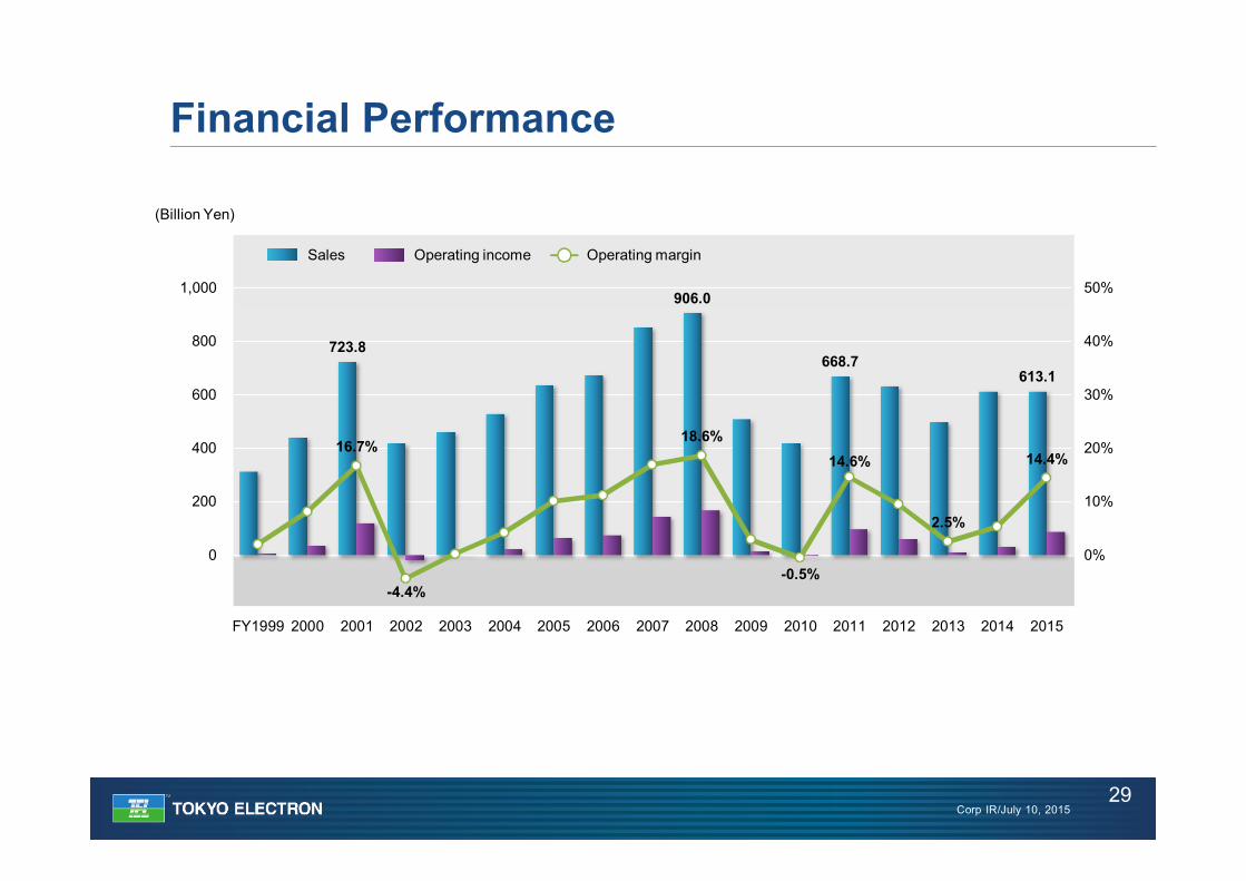
723.8
906.0
668.7613.1
16.7%
-4.4%
18.6%
-0.5%
14.6%
2.5%
14.4%
-10%
0%
10%
20%
30%
40%
50%
60%
-200
0
200
400
600
800
1,000
1,200
FY1999 2000 2001 2002 2003 2004 2005 2006 2007 2008 2009 2010 2011 2012 2013 2014 2015
Financial Performance
29
(Billion Yen)
Sales Operating income Operating margin
Corp IR/July 10, 2015
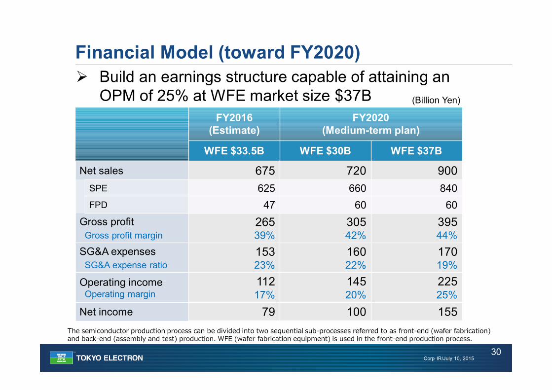
Build an earnings structure capable of attaining anOPM of 25% at WFE market size $37B
Financial Model (toward FY2020)
30
FY2016(Estimate)
FY2020(Medium-term plan)
WFE $33.5B WFE $30B WFE $37B
Net sales 675 720 900SPE 625 660 840FPD 47 60 60
Gross profitGross profit margin
26539%
30542%
39544%
SG&A expensesSG&A expense ratio
15323%
16022%
17019%
Operating incomeOperating margin
11217%
14520%
22525%
Net income 79 100 155
(Billion Yen)
The semiconductor production process can be divided into two sequential sub-processes referred to as front-end (wafer fabrication) and back-end (assembly and test) production. WFE (wafer fabrication equipment) is used in the front-end production process.

Corp IR/July 10, 2015
SPE Sales (WFE $37B)
31
FY2016(Estimate)
FY2020(Medium-term
plan)Growth
WFE $33.5B WFE $37B WFE +10%
Sales 625 840 +34%
New equipment 465 650 +40%
Field solutions 160 190 +19%
Sales growth in excess of market growth(Billion Yen)
• Enhance our ability to identify the technological needs of our customers and to develop products to meet them
• Respond to growing demand for field solutions
Corp IR/July 10, 2015
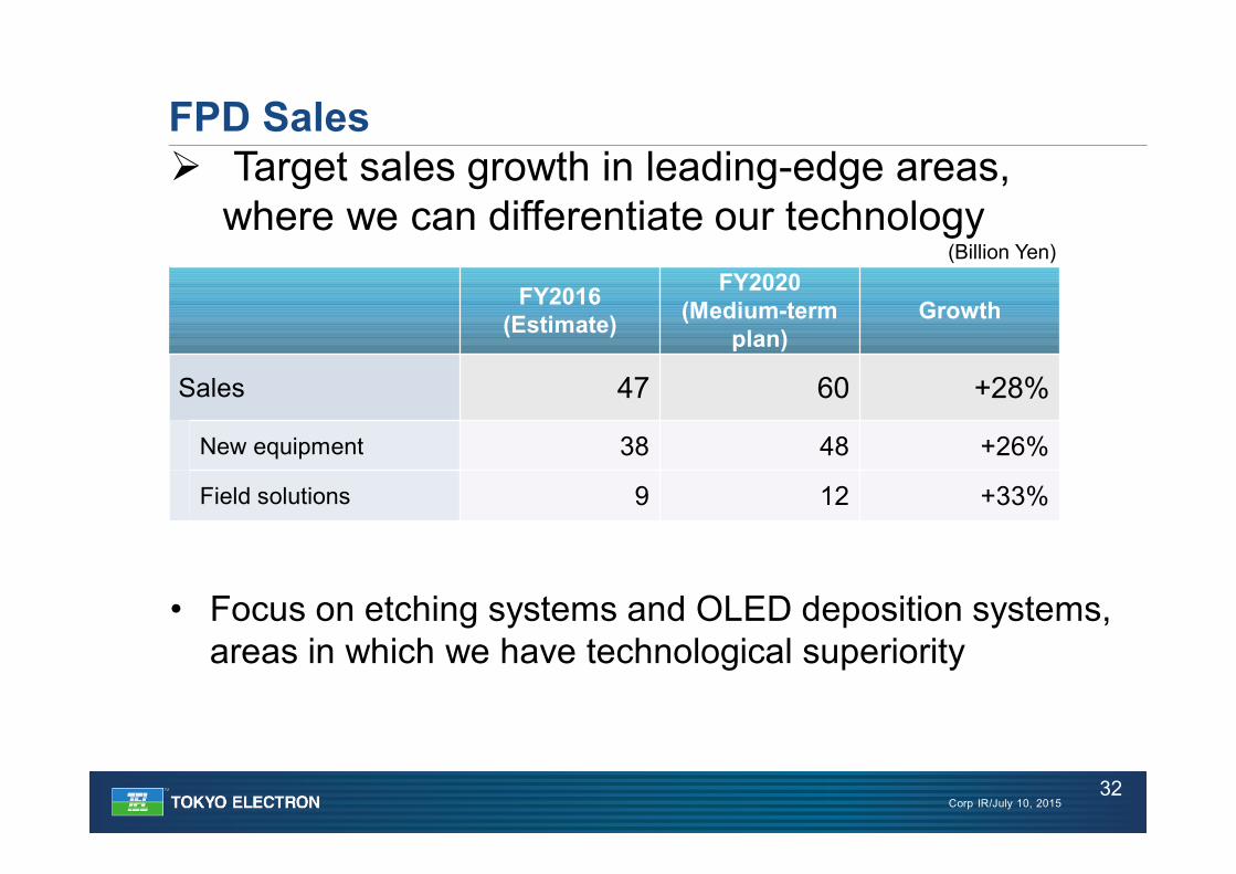
FPD Sales
32
FY2016(Estimate)
FY2020(Medium-term
plan)Growth
Sales 47 60 +28%
New equipment 38 48 +26%
Field solutions 9 12 +33%
Target sales growth in leading-edge areas, where we can differentiate our technology
(Billion Yen)
• Focus on etching systems and OLED deposition systems, areas in which we have technological superiority

Corp IR/July 10, 2015
Gross Profit (WFE $37B)
33
Gross profit margin: up 5%pts
FY2016(Estimate)
FY2020(Medium-term
plan)Growth
Gross profitGross profit margin
26539%
39544%
+49%+5%pts
(Billion Yen)
• Raise marginal profit ratio through efforts to enhance product competitiveness
• Expand field solutions business
• Reduce costs by sharing technology across our products
• Reduce costs, shorten production lead-times and pursue quality from the design stage onward
Corp IR/July 10, 2015
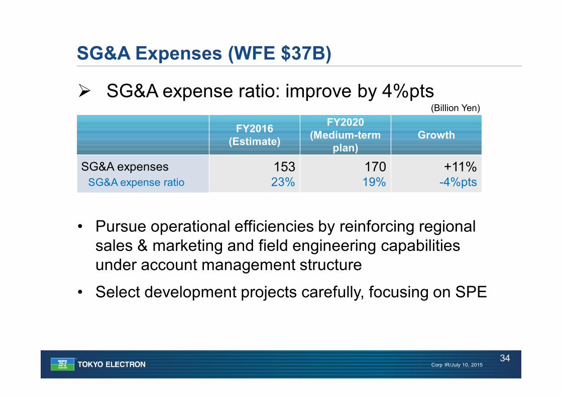
SG&A Expenses (WFE $37B)
34
SG&A expense ratio: improve by 4%pts
FY2016(Estimate)
FY2020(Medium-term
plan)Growth
SG&A expensesSG&A expense ratio
15323%
17019%
+11%-4%pts
(Billion Yen)
• Pursue operational efficiencies by reinforcing regional sales & marketing and field engineering capabilities under account management structure
• Select development projects carefully, focusing on SPE
Corp IR/July 10, 2015
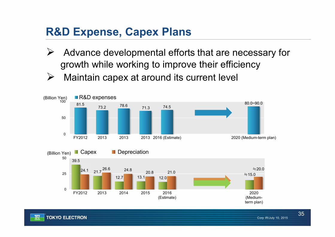
R&D Expense, Capex Plans
35
81.573.2 78.6 71.3 74.5
80.0~90.0
0
50
100
FY2012 2013 2013 2013 2016 (Estimate) 2020 (Medium-term plan)
R&D expenses(Billion Yen)
39.5
21.712.7 13.1 12.0
≒15.024.1 26.6 24.8 20.8 21.0
≒20.0
0
25
50
FY2012 2013 2014 2015 2016(Estimate)
2020(Medium-term plan)
DepreciationCapex(Billion Yen)
Advance developmental efforts that are necessary for growth while working to improve their efficiency
Maintain capex at around its current level

Corp IR/July 10, 2015
Managerial Targets
36
$30B $37BWFE Market
Operating margin
ROE
20% 25%
15% 20%
We target a global level of profitability
The semiconductor production process can be divided into two sequential sub-processes referred to as front-end (wafer fabrication) and back-end (assembly and test) production. WFE (wafer fabrication equipment) is used in the front-end production process.
Corp IR/July 10, 2015
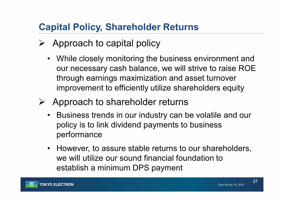
Approach to capital policy• While closely monitoring the business environment and
our necessary cash balance, we will strive to raise ROE through earnings maximization and asset turnover improvement to efficiently utilize shareholders equity
Approach to shareholder returns• Business trends in our industry can be volatile and our
policy is to link dividend payments to business performance
• However, to assure stable returns to our shareholders, we will utilize our sound financial foundation to establish a minimum DPS payment
Capital Policy, Shareholder Returns
37

Corp IR/July 10, 2015
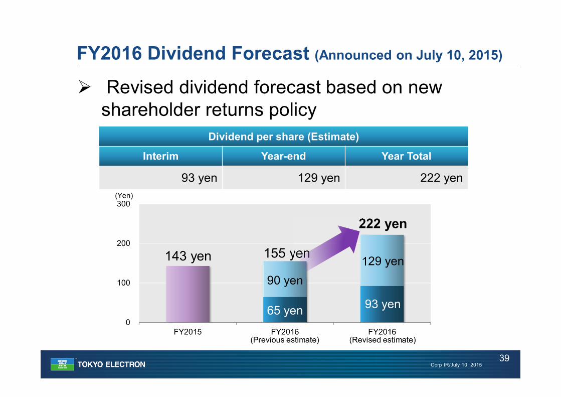
New Policy for Shareholder Returns
38
Dividend payout ratio:
Annual DPS of not less than ¥150We will review our dividend policy if the company does
not generate net income for two consecutive fiscal years
50%
We will flexibly consider share buybacks
Our previous dividend policy since FY2011 year-end dividend was performance-linked payout ratio of around 35%.
Corp IR/July 10, 2015
0
100
200
300
FY2015 FY2016 FY2016
155 yen
90 yen
65 yen
FY2016 Dividend Forecast (Announced on July 10, 2015)
39
(Yen)
Dividend per share (Estimate)
Interim Year-end Year Total
93 yen 129 yen 222 yen
143 yen
222 yen
129 yen
93 yen
Revised dividend forecast based on new shareholder returns policy
(Previous estimate) (Revised estimate)
Corp IR/July 10, 2015
Summary
40
We strive to outperform market growth and enhance our corporate value
Corp IR/July 10, 2015
Disclaimer regarding forward-looking statementForecast of TEL’s performance and future prospects and other sort of information published are made based on information available at the time of publication. Actual performance and results may differ significantly from the forecast described here due to changes in various external and internal factors, including the economic situation, semiconductor/FPD/PV market conditions, intensification of sales competition, safety and product quality management, and intellectual property-related risks.
Processing of numbersFor the amount listed, because fractions are rounded down, there may be the cases where the total for certain account titles does not correspond to the sum of the respective figures for account titles. Percentages are calculated using full amounts, before rounding.
Exchange RiskIn principle, export sales of Tokyo Electron’s mainstay semiconductor and FPD/PV panel production equipment are denominated in yen. While some settlements are denominated in dollars, exchange risk is hedged as forward exchange contracts are made individually at the time of booking. Accordingly, the effect of exchange rates on profits is negligible.
FPD/PV: Flat panel display/Photovoltaic