CPE100: Digital Logic Design Ib1morris/cpe100/slides/slides_review_final_v2.pdf · Ch 1.5 Logic...
29
http://www.ee.unlv.edu/~b1morris/cpe100/ Professor Brendan Morris, SEB 3216, [email protected] CPE100: Digital Logic Design I Final Review
Transcript of CPE100: Digital Logic Design Ib1morris/cpe100/slides/slides_review_final_v2.pdf · Ch 1.5 Logic...
http://www.ee.unlv.edu/~b1morris/cpe100/
Professor Brendan Morris, SEB 3216, [email protected]
CPE100: Digital Logic Design I
Final Review

Logistics
• Tuesday Dec 12th
▫ 13:00-15:00 (1-3pm)
▫ 2 hour exam
• Chapters 1-3, 5.4.1
▫ Responsible for all material
• Closed book, closed notes
• No calculators
• Must show work and be legible for credit
2

Preparation
• Read the book (2nd Edition) ▫ Then, read it again
• Do example problems ▫ Use both Harris and Roth books
• Be sure you understand homework solutions
• Come visit during office hours for questions
• Exam Advice: Be sure to attempt all problems. ▫ Partial credit can only be given for something written
on the page ▫ Don’t spend too much time thinking ▫ Be sure to read questions completely
3

Main New Material
• Synchronous timing
▫ How can you ensure dynamic discipline is respected
• Parallelism
▫ How can you increase operational speed
• Synchronous building blocks
▫ Full-adder, counter
4

Ch 3.5.2 Synchronous Timing
• Data input must be stabled when sampled at rising clock edge
• Setup time: 𝑡𝑠𝑒𝑡𝑢𝑝 = time before clock edge data
must be stable (i.e. not changing)
• Hold time: 𝑡ℎ𝑜𝑙𝑑 = time after clock edge data must be stable
5
CLK
tsetup
D
thold
ta

Timing Constraints
• Setup Timing • 𝐷2 cannot change 𝑡𝑠𝑒𝑡𝑢𝑝 before
next clock cycle
• 𝑇𝑐 ≥ 𝑡𝑝𝑐𝑞 + 𝑡𝑝𝑑 + 𝑡𝑠𝑒𝑡𝑢𝑝
• Hold Timing • 𝐷2 cannot change until after 𝑡ℎ𝑜𝑙𝑑 of the current clock cycle
• 𝑡ℎ𝑜𝑙𝑑 < 𝑡𝑐𝑐𝑞 + 𝑡𝑐𝑑
6
CLK
Q1
D2
Tc
tpcq
tpd
tsetup
CL
CLKCLK
Q1 D2
R1 R2
CLK
Q1
D2
tccq
tcd
thold
CL
CLKCLK
Q1 D2
R1 R2

Ch 3.6 Parallelism
• Goal is to increase throughput of circuit • Two types:
▫ Spatial – duplicate hardware to do same task at once
▫ Temporal – break task into smaller stages for pipelining (assembly line) Note: this requires no dependencies between stages
• Token – group of inputs processed to produce group of outputs
• Latency – time for a single token to complete • Throughput – # tokens produced per unit time
7
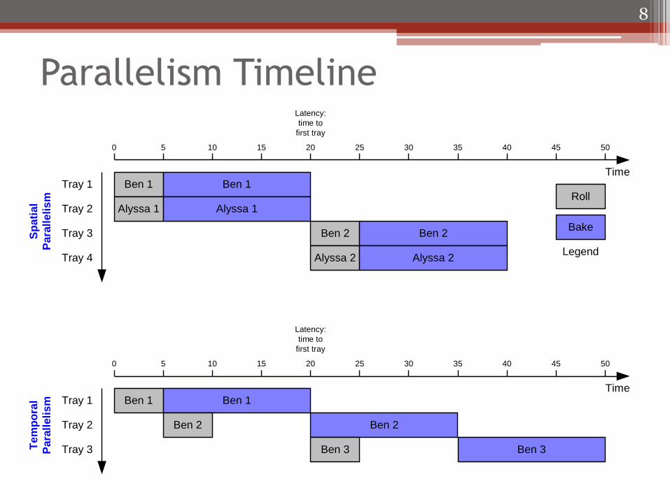
Parallelism Timeline
8 S
pa
tial
Para
lleli
sm Roll
Bake
Ben 1 Ben 1
Alyssa 1 Alyssa 1
Ben 2 Ben 2
Alyssa 2 Alyssa 2
Time
0 5 10 15 20 25 30 35 40 45 50
Tray 1
Tray 2
Tray 3
Tray 4
Latency:
time to
first tray
Legend
Te
mp
ora
l
Para
lleli
sm Ben 1 Ben 1
Ben 2 Ben 2
Ben 3 Ben 3
Time
0 5 10 15 20 25 30 35 40 45 50
Latency:
time to
first tray
Tray 1
Tray 2
Tray 3

Pipeline Example
• 𝑡𝑝𝑐𝑞 = 0.3, 𝑡𝑠𝑒𝑡𝑢𝑝 = 0.2 ns
• Identify critical path
9

Pipeline Example II
• Two-stage pipeline
10

Pipeline Example III
• Three-stage pipeline
11
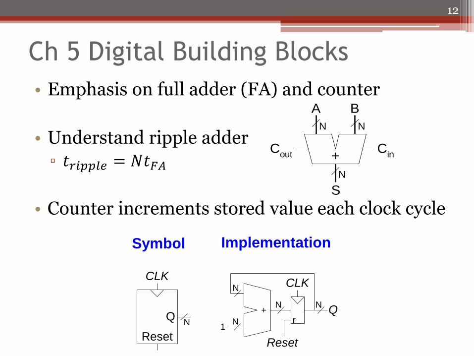
Ch 5 Digital Building Blocks
• Emphasis on full adder (FA) and counter
• Understand ripple adder
▫ 𝑡𝑟𝑖𝑝𝑝𝑙𝑒 = 𝑁𝑡𝐹𝐴
• Counter increments stored value each clock cycle
12
Q
CLK
Reset
N
+
N
1
CLK
Reset
N
N
QN
r
Symbol Implementation
A B
S
Cout
Cin+
N
NN

Chapter 3.4 Finite State Machine
• Technique for representing synchronous sequential circuit
▫ Consists of combinational logic and state register
▫ Moore machine – output only dependent on state (not inputs)
13

Chapter 3.4 FSM Design Steps
1. Identify inputs and outputs
2. Sketch state transition diagram
3. Write state transition table
4. Select state encodings
5. Rewrite state transition table with state encodings
6. Write output table
7. Write Boolean equations for next state and output
logic
8. Sketch the circuit schematic
14

Chapter 3.4 FSM Examples
• Given problem description, give state transition diagram
• Given state transition diagram, encode state and provide next state/output equations
• Given FSM circuit, describe what system does and give state transition/output tables
15

Chapter 3.4 FSM Examples
• Design and edge detector circuit. The output should go HIGH for one cycle after the input makes a 0 → 1 transition.
• Single input: A
16
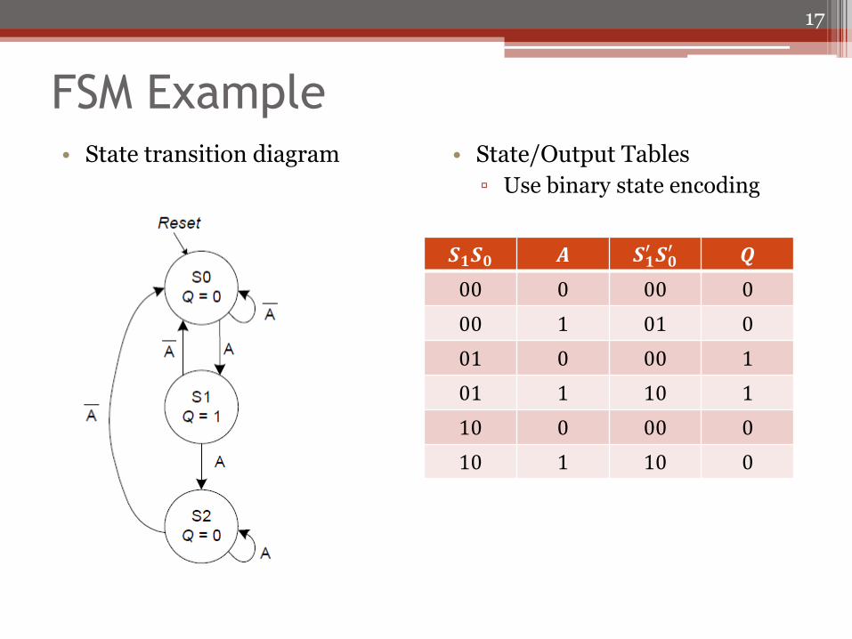
FSM Example • State transition diagram • State/Output Tables
▫ Use binary state encoding
17
𝑺𝟏𝑺𝟎 𝑨 𝑺𝟏′ 𝑺𝟎
′ 𝑸
00 0 00 0
00 1 01 0
01 0 00 1
01 1 10 1
10 0 00 0
10 1 10 0
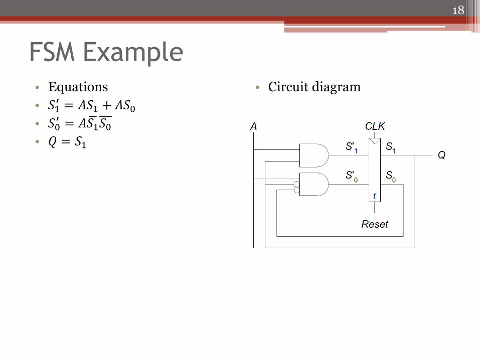
FSM Example • Equations
• 𝑆1′ = 𝐴𝑆1 + 𝐴𝑆0
• 𝑆0′ = 𝐴𝑆1 𝑆0
• 𝑄 = 𝑆1
• Circuit diagram
18

Ch 1.4 Number Systems
• General number representation
▫ N-digit number {𝑎𝑁−1𝑎𝑁−2…𝑎1𝑎0} of base 𝑅 in decimal
𝑎𝑁−1𝑅𝑁−1 + 𝑎𝑁−2𝑅
𝑁−2 +⋯+ 𝑎1𝑅1 + 𝑎0𝑅
0
= 𝑎𝑖𝑅𝑖𝑁−1
𝑖=0
▫ What is range of values?
• Should be very familiar with common bases such as 2, 10, 16
▫ Be able to convert between bases
19

Number Example
• What is 101102 in (unsigned) decimal?
• Convert 101102 to base 6
20
Binary Addition
• Understand signed number representation (unsigned, two’s complement, sign-mag)
• Addition ▫ Potential for overflow – know how and when
occurs
• Subtraction
▫ Find negative of number and do addition
• Zero/sign extension – when should you use
which?
21

Binary Addition Example
• Assume 4-bit 2’s complement and indicate if overflow occurs
• Add −8 + 4
22

Ch 1.5 Logic Gates
• Know circuit symbols and associated truth tables
▫ NOT/BUF, AND/OR, NAND/NOR, XOR, XNOR
• Be able to determine output from gate level circuit schematic
▫ Both give truth table and provide Boolean equation
23

Ch 2.3-2.4 Boolean Equations
• Sum-of-product (SOP) minterm form
• Product-of-sum (POS) maxterm form
• Simplify using axioms/theorms
• Example
24
A B C Y
0 0 0 0
0 0 1 0
0 1 0 0
0 1 1 1
1 0 0 0
1 0 1 1
1 1 0 1
1 1 1 1

Ch 2.7 Kmap
• Convert truth table to Kmap and draw bubbles to maximally cover ones
▫ Be sure to know how to include don’t cares
▫ Know up to 5-input function
• Example
25
A B C Y
0 0 0 0
0 0 1 0
0 1 0 0
0 1 1 1
1 0 0 0
1 0 1 1
1 1 0 1
1 1 1 1

Ch 2.8 Mux/Decoder
• Know how to do logic with mux or decoder
• Mux
• Decoder
26
Ch 2.9 Combinational Timing
• Delay for input to cause a change in output
• Propagation delay 𝑡𝑝𝑑 is longest time to see
output change
• Contamination delay 𝑡𝑐𝑑 is shortest time to see output change
27
Ch 3.2 Sequential Elements
• Sequential elements store “state” – have memory
• Need to know the operation of different devices
▫ SR latch, D latch, D flip-flop
• Should also understand the internal circuitry for these elements
▫ Given a sequential circuit design you can explain operation
▫ Given a description of operation, build a circuit using sequential building blocks.
28

Sequential Element Example
• How does the following work?
29