CP2112 Data Sheet - docs.rs-online.com
22
Rev. 1.2 11/13 Copyright © 2013 by Silicon Laboratories CP2112 CP2112 S INGLE -C HIP HID USB TO SMB US M ASTER B RIDGE Single-Chip HID USB to SMBus Master Bridge Integrated USB transceiver; no external resistors or crystal required SMBus master device GPIO can be configured as Input/Output and Open- Drain/Push-Pull 512 Byte SMBus data buffer Integrated 194 Byte One-Time Programmable ROM for storing customizable product information On-chip power-on reset circuit On-chip voltage regulator: 3.45 V output USB Peripheral Function Controller USB Specification 2.0 compliant; full-speed (12 Mbps) USB Suspend states supported via SUSPEND and SUSPEND pins HID Interface Standard USB class device requires no custom driver Windows 7, Vista, XP, Server 2003, 2000 Win CE 6.0, 5.0, and 4.2 Mac OS X Linux Open access to interface specification Windows and Mac HID-to-SMBus Libraries APIs for quick application development Supports Windows 7, Vista, XP, Server 2003, 2000 Supports Mac OS X SMBus Configuration Options Configurable Clock Speed Device Address: 7-bit value that is the slave address of the CP2112. The device will only ACK this address, but will not respond to any read/write requests Read/Write Timeouts SCL Low Timeout Retry Counter Timeout GPIO Interface Features 8 GPIO pins with configurable options Usable as inputs, open-drain or push-pull outputs Configurable clock output for external devices - 48 MHz to 94 kHz Toggle LED during SMBus reads Toggle LED during SMBus writes Supply Voltage Self-powered: 3.0 to 3.6 V USB bus powered: 4.0 to 5.25 V I/O voltage: 1.8 V to V DD Ordering Part Number CP2112-F02-GM Package RoHS-compliant 24-pin QFN (4 x 4 mm) Temperature Range: –40 to +85 °C Figure 1. Example System Diagram Connect to VBUS or External Supply VBUS D+ D- GND USB Connector GPIO Signals CP2112 48 MHz Oscillator SMBus Controller Voltage Regulator REGIN VDD GND VBUS D+ D- RST GPIO and Suspend Controller SDA SCL GPIO.0_TXT GPIO.1_RXT GPIO.2 GPIO.3 GPIO.4 GPIO.5 GPIO.6 GPIO.7_CLK Suspend Signals SUSPEND SUSPEND USB Interface Peripheral Function Controller Full-Speed 12 Mbps Transceiver 194 Byte PROM (Product Customization) VPP Logic Level Supply (1.8V to VDD) VIO I/O Power and Logic Levels To SMBus Slave Devices
Transcript of CP2112 Data Sheet - docs.rs-online.com
CP2112
SINGLE-CHIP HID USB TO SMBUS MASTER BRIDGE
Single-Chip HID USB to SMBus Master BridgeIntegrated USB transceiver; no external resistors or
crystal requiredSMBus master deviceGPIO can be configured as Input/Output and Open-
Drain/Push-Pull512 Byte SMBus data bufferIntegrated 194 Byte One-Time Programmable ROM for
storing customizable product informationOn-chip power-on reset circuitOn-chip voltage regulator: 3.45 V output
USB Peripheral Function ControllerUSB Specification 2.0 compliant; full-speed (12 Mbps)USB Suspend states supported via SUSPEND and
SUSPEND pins
HID InterfaceStandard USB class device requires no custom driverWindows 7, Vista, XP, Server 2003, 2000Win CE 6.0, 5.0, and 4.2Mac OS XLinuxOpen access to interface specification
Windows and Mac HID-to-SMBus LibrariesAPIs for quick application developmentSupports Windows 7, Vista, XP, Server 2003, 2000Supports Mac OS X
SMBus Configuration OptionsConfigurable Clock SpeedDevice Address: 7-bit value that is the slave address of
the CP2112. The device will only ACK this address, but will not respond to any read/write requests
Read/Write TimeoutsSCL Low TimeoutRetry Counter Timeout
GPIO Interface Features8 GPIO pins with configurable optionsUsable as inputs, open-drain or push-pull outputsConfigurable clock output for external devices
- 48 MHz to 94 kHzToggle LED during SMBus readsToggle LED during SMBus writes
Supply VoltageSelf-powered: 3.0 to 3.6 VUSB bus powered: 4.0 to 5.25 VI/O voltage: 1.8 V to VDD
Ordering Part NumberCP2112-F02-GM
PackageRoHS-compliant 24-pin QFN (4 x 4 mm)
Temperature Range: –40 to +85 °C
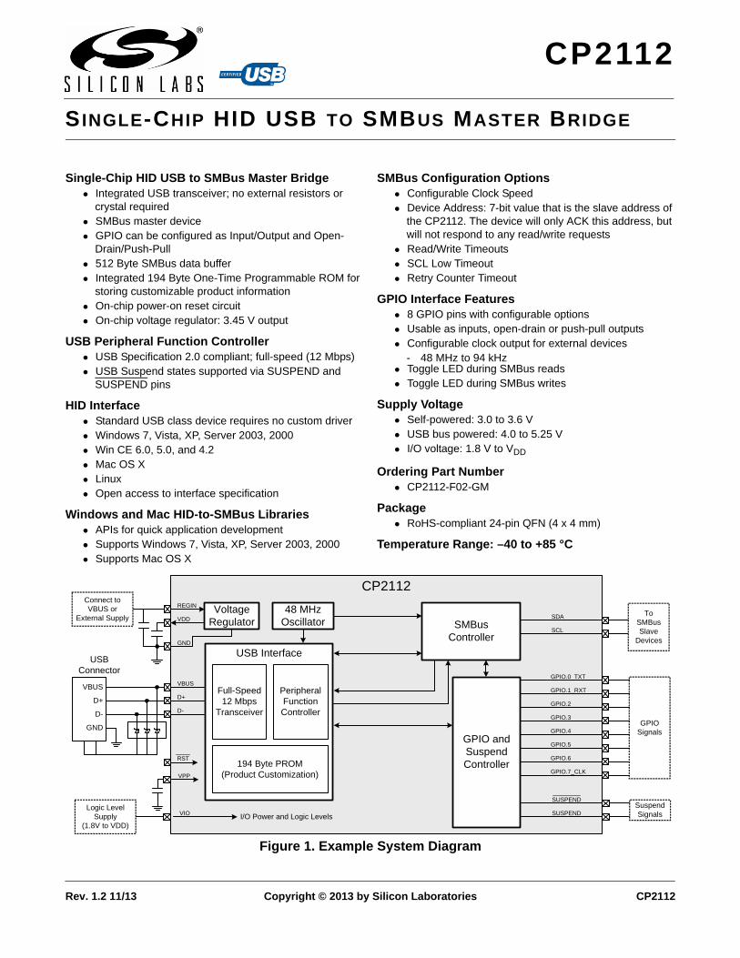
Figure 1. Example System Diagram
Connect to VBUS or
External Supply
VBUS
D+
D-
GND
USB Connector
GPIO Signals
CP2112
48 MHz Oscillator SMBus
Controller
Voltage Regulator
REGIN
VDD
GND
VBUS
D+
D-
I/O Power and Logic Levels
RST
GPIO and Suspend Controller
SDA
SCL
GPIO.0_TXT
GPIO.1_RXT
GPIO.2
GPIO.3
GPIO.4
GPIO.5
GPIO.6
GPIO.7_CLK
Suspend Signals
SUSPEND
SUSPEND
USB Interface
Peripheral Function Controller
Full-Speed 12 Mbps
Transceiver
194 Byte PROM(Product Customization)VPP
Logic Level Supply
(1.8V to VDD)
VIO I/O Power and Logic Levels
To SMBus Slave
Devices
Rev. 1.2 11/13 Copyright © 2013 by Silicon Laboratories CP2112
CP2112
2 Rev. 1.2

CP2112
TABLE OF CONTENTS
Section Page
1. System Overview . . . . . . . . . . . . . . . . . . . . . . . . . . . . . . . . . . . . . . . . . . . . . . . . . . . . . . . . .42. Electrical Characteristics . . . . . . . . . . . . . . . . . . . . . . . . . . . . . . . . . . . . . . . . . . . . . . . . . .53. Pinout and Package Definitions . . . . . . . . . . . . . . . . . . . . . . . . . . . . . . . . . . . . . . . . . . . . .84. QFN-24 Package Specifications . . . . . . . . . . . . . . . . . . . . . . . . . . . . . . . . . . . . . . . . . . . .115. USB Function Controller and Transceiver . . . . . . . . . . . . . . . . . . . . . . . . . . . . . . . . . . . .136. System Management Bus (SMBus) Interface . . . . . . . . . . . . . . . . . . . . . . . . . . . . . . . . .13
6.1. SMBus Configuration . . . . . . . . . . . . . . . . . . . . . . . . . . . . . . . . . . . . . . . . . . . . . . . .136.2. SMBus Operation . . . . . . . . . . . . . . . . . . . . . . . . . . . . . . . . . . . . . . . . . . . . . . . . . . .146.3. CP2112 Configuration Options . . . . . . . . . . . . . . . . . . . . . . . . . . . . . . . . . . . . . . . . .15
7. GPIO Pins . . . . . . . . . . . . . . . . . . . . . . . . . . . . . . . . . . . . . . . . . . . . . . . . . . . . . . . . . . . . . .167.1. GPIO.0-1—Transmit and Receive Toggle . . . . . . . . . . . . . . . . . . . . . . . . . . . . . . . .167.2. GPIO.7—Clock Output . . . . . . . . . . . . . . . . . . . . . . . . . . . . . . . . . . . . . . . . . . . . . . .16
8. One-Time Programmable ROM . . . . . . . . . . . . . . . . . . . . . . . . . . . . . . . . . . . . . . . . . . . . .179. Voltage Regulator . . . . . . . . . . . . . . . . . . . . . . . . . . . . . . . . . . . . . . . . . . . . . . . . . . . . . . . .1810. CP2112 Interface Specification and Windows Interface DLL . . . . . . . . . . . . . . . . . . . .2011. Relevant Application Notes and Software . . . . . . . . . . . . . . . . . . . . . . . . . . . . . . . . . . .2012. Device Specific Behavior . . . . . . . . . . . . . . . . . . . . . . . . . . . . . . . . . . . . . . . . . . . . . . . . .20
12.1. Addressed Read Requests . . . . . . . . . . . . . . . . . . . . . . . . . . . . . . . . . . . . . . . . . . .2012.2. Multimaster Applications . . . . . . . . . . . . . . . . . . . . . . . . . . . . . . . . . . . . . . . . . . . . .20
Document Change List . . . . . . . . . . . . . . . . . . . . . . . . . . . . . . . . . . . . . . . . . . . . . . . . . . . . .21Contact Information . . . . . . . . . . . . . . . . . . . . . . . . . . . . . . . . . . . . . . . . . . . . . . . . . . . . . . . .22
Rev. 1.2 3
CP2112
1. System Overview
The CP2112 is a highly-integrated HID USB-to-SMBus Bridge providing a simple solution for controlling SMBusslave devices with USB and using a minimum of components and PCB space. The CP2112 includes a USB 2.0full-speed function controller, USB transceiver, oscillator, and a one-time programmable ROM in a compact4 x 4 mm QFN-24 package (sometimes called “MLF” or “MLP”).
The on-chip, one-time programmable ROM provides the option to customize the USB Vendor ID, Product ID,Manufacturer Product String, Product Description String, Power Descriptor, Device Release Number, and DeviceSerial Number as desired for OEM applications.
The CP2112 uses the standard USB HID device class, which is natively supported by most operating systems. Acustom driver does not need to be installed for this device. Windows applications communicate with the CP2112through a Windows DLL, which is provided by Silicon Labs. The interface specification for the CP2112 is alsoavailable to enable development of an API for any operating system that supports HID.
The CP2112 SMBus interface includes the SDA and SCL signals needed for SMBus communication and isconfigurable. The configurable options include the clock speed, read/write timeouts, retry counter timeout, SCL lowtimeouts, and a 7-bit device address. The CP2112 will only ACK the 7-bit device address assigned to it but will notrespond to any read/write requests. External pull-up resistors are needed for the SCL and SDA signals.
The device also features a total of eight GPIO signals. The GPIO signals are controlled through USB and can beconfigured as Input/Output and Open-Drain/Push-Pull. Three of the GPIO signals support alternate featuresincluding a configurable clock output (48 MHz to 94 kHz) and TX and RX LED toggle. Support for I/O interfacevoltages down to 1.8 V is provided via a VIO pin.
An evaluation kit for the CP2112 (Part Number: CP2112EK) is available. It includes a CP2112-based HID USB-to-SMBus evaluation board, Windows DLL and test application, USB cable, and full documentation. Go towww.silabs.com for the latest application notes and product support information for the CP2112. Contact a SiliconLabs sales representatives or go to www.silabs.com to order the CP2112 Evaluation Kit.
4 Rev. 1.2
CP2112
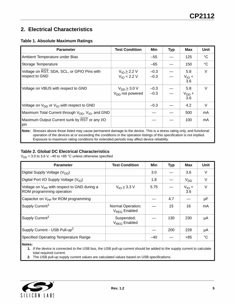
2. Electrical Characteristics
Table 1. Absolute Maximum Ratings
Parameter Test Condition Min Typ Max Unit
Ambient Temperature under Bias –55 — 125 °C
Storage Temperature –65 — 150 °C
Voltage on RST, SDA, SCL, or GPIO Pins with respect to GND
VIO > 2.2 VVIO < 2.2 V
–0.3–0.3
——
5.8VIO + 3.6
V
Voltage on VBUS with respect to GND VDD > 3.0 VVDD not powered
–0.3–0.3
——
5.8VDD +
3.6
V
Voltage on VDD or VIO with respect to GND –0.3 — 4.2 V
Maximum Total Current through VDD, VIO, and GND — — 500 mA
Maximum Output Current sunk by RST or any I/O pin
— — 100 mA
Note: Stresses above those listed may cause permanent damage to the device. This is a stress rating only, and functional operation of the devices at or exceeding the conditions in the operation listings of this specification is not implied. Exposure to maximum rating conditions for extended periods may affect device reliability.
Table 2. Global DC Electrical CharacteristicsVDD = 3.0 to 3.6 V, –40 to +85 °C unless otherwise specified
Parameter Test Condition Min Typ Max Unit
Digital Supply Voltage (VDD) 3.0 — 3.6 V
Digital Port I/O Supply Voltage (VIO) 1.8 — VDD V
Voltage on VPP with respect to GND during aROM programming operation
VIO > 3.3 V 5.75 — VIO + 3.6
V
Capacitor on VPP for ROM programming — 4.7 — µF
Supply Current1 Normal Operation; VREG Enabled
— 15 16 mA
Supply Current1 Suspended;VREG Enabled
— 130 230 µA
Supply Current - USB Pull-up2 — 200 228 µA
Specified Operating Temperature Range –40 — +85 °C
Notes:1. If the device is connected to the USB bus, the USB pull-up current should be added to the supply current to calculate
total required current.2. The USB pull-up supply current values are calculated values based on USB specifications.
Rev. 1.2 5

CP2112
Table 3. SMBus, Suspend I/O DC Electrical CharacteristicsVDD = 3.0 to 3.6 V, VIO = 1.8 V to VDD, –40 to +85 °C unless otherwise specified.
Parameter Test Condition Min Typ Max Unit
Output High Voltage (VOH) IOH = –10 µAIOH = –3 mAIOH = –10 mA
VIO – 0.1VIO – 0.2
—
——
VIO – 0.4
———
V
Output Low Voltage (VOL) IOL = 10 µAIOL = 8.5 mAIOL = 25 mA
———
——0.6
0.10.4—
V
Input High Voltage (VIH) 0.7 x VIO — — V
Input Low Voltage (VIL) — — 0.6 V
Input Leakage Current Weak Pull-Up OffWeak Pull-Up On, VIO = 0 V
——
—25
150
µAµA
Maximum Input Voltage Open drain, logic high (1) — — 5.8 V
Table 4. Reset Electrical Characteristics–40 to +85 °C unless otherwise specified
Parameter Test Condition Min Typ Max Unit
RST Input High Voltage 0.75 x VIO — — V
RST Input Low Voltage — — 0.6 V
Minimum RST Low Time to Generate a System Reset
15 — — µs
VDD Ramp Time for Power On
— — 1 ms
Table 5. Voltage Regulator Electrical Specifications–40 to +85 °C unless otherwise specified
Parameter Test Condition Min Typ Max Unit
Input Voltage Range 3.0 — 5.25 V
Output Voltage Output Current = 1 to 100 mA* 3.3 3.45 3.6 V
VBUS Detection Input Threshold 2.5 — — V
Bias Current — — 120 µA
*Note: The maximum regulator supply current is 100 mA. This includes the supply current of the CP2112.
6 Rev. 1.2
CP2112
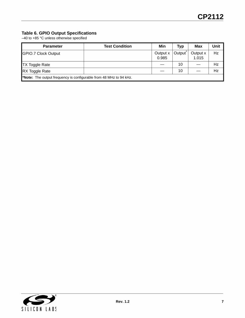
Table 6. GPIO Output Specifications–40 to +85 °C unless otherwise specified
Parameter Test Condition Min Typ Max Unit
GPIO.7 Clock Output Output x 0.985
Output* Output x 1.015
Hz
TX Toggle Rate — 10 — Hz
RX Toggle Rate — 10 — Hz
*Note: The output frequency is configurable from 48 MHz to 94 kHz.
Rev. 1.2 7
CP2112
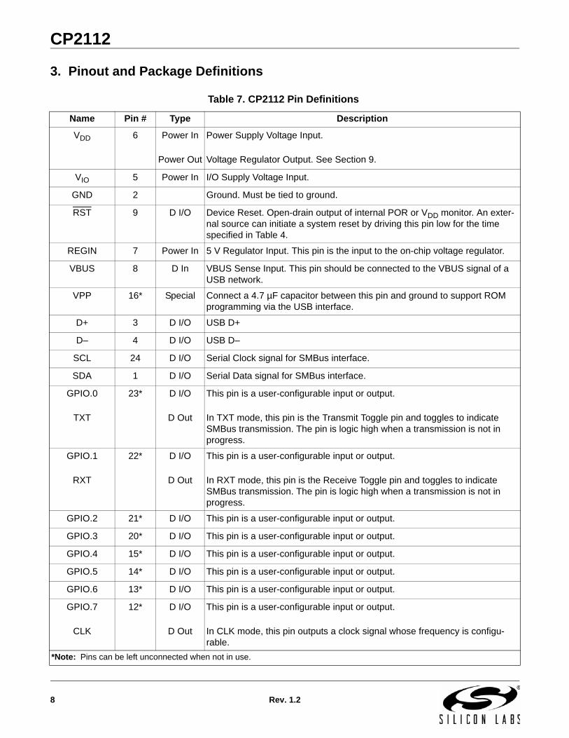
3. Pinout and Package Definitions
Table 7. CP2112 Pin Definitions
Name Pin # Type Description
VDD 6 Power In
Power Out
Power Supply Voltage Input.
Voltage Regulator Output. See Section 9.
VIO 5 Power In I/O Supply Voltage Input.
GND 2 Ground. Must be tied to ground.
RST 9 D I/O Device Reset. Open-drain output of internal POR or VDD monitor. An exter-nal source can initiate a system reset by driving this pin low for the time specified in Table 4.
REGIN 7 Power In 5 V Regulator Input. This pin is the input to the on-chip voltage regulator.
VBUS 8 D In VBUS Sense Input. This pin should be connected to the VBUS signal of a USB network.
VPP 16* Special Connect a 4.7 µF capacitor between this pin and ground to support ROM programming via the USB interface.
D+ 3 D I/O USB D+
D– 4 D I/O USB D–
SCL 24 D I/O Serial Clock signal for SMBus interface.
SDA 1 D I/O Serial Data signal for SMBus interface.
GPIO.0
TXT
23* D I/O
D Out
This pin is a user-configurable input or output.
In TXT mode, this pin is the Transmit Toggle pin and toggles to indicate SMBus transmission. The pin is logic high when a transmission is not in progress.
GPIO.1
RXT
22* D I/O
D Out
This pin is a user-configurable input or output.
In RXT mode, this pin is the Receive Toggle pin and toggles to indicate SMBus transmission. The pin is logic high when a transmission is not in progress.
GPIO.2 21* D I/O This pin is a user-configurable input or output.
GPIO.3 20* D I/O This pin is a user-configurable input or output.
GPIO.4 15* D I/O This pin is a user-configurable input or output.
GPIO.5 14* D I/O This pin is a user-configurable input or output.
GPIO.6 13* D I/O This pin is a user-configurable input or output.
GPIO.7
CLK
12* D I/O
D Out
This pin is a user-configurable input or output.
In CLK mode, this pin outputs a clock signal whose frequency is configu-rable.
*Note: Pins can be left unconnected when not in use.
8 Rev. 1.2
CP2112
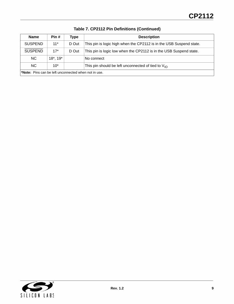
SUSPEND 11* D Out This pin is logic high when the CP2112 is in the USB Suspend state.
SUSPEND 17* D Out This pin is logic low when the CP2112 is in the USB Suspend state.
NC 18*, 19* No connect
NC 10* This pin should be left unconnected of tied to VIO
Table 7. CP2112 Pin Definitions (Continued)
Name Pin # Type Description
*Note: Pins can be left unconnected when not in use.
Rev. 1.2 9
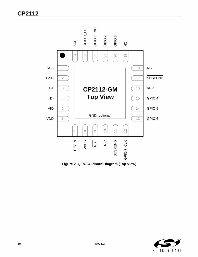
CP2112
Figure 2. QFN-24 Pinout Diagram (Top View)
24 23 22 21 20 19
1
2
3
4
5
6
7 8 9 10
11
12
18
17
16
15
14
13GND (optional)
CP2112-GMTop View
NC
GP
IO.3
GP
IO.2
GP
IO.1
_RX
T
GP
IO.0
_TX
T
SC
L
SDA
GND
D+
N/C
SU
SP
EN
D
GP
IO.7
_C
LK
NC
GPIO.6
GPIO.5
GPIO.4
VPP
SUSPEND
VDD
VIO
D-R
ST
VB
US
RE
GIN
10 Rev. 1.2

CP2112
4. QFN-24 Package Specifications
Figure 3. QFN-24 Package Drawing
Table 8. QFN-24 Package Dimensions
Dimension Min Typ Max Dimension Min Typ Max
A 0.70 0.75 0.80 L 0.30 0.40 0.50
A1 0.00 0.02 0.05 L1 0.00 — 0.15
b 0.18 0.25 0.30 aaa — — 0.15
D 4.00 BSC. bbb — — 0.10
D2 2.55 2.70 2.80 ddd — — 0.05
e 0.50 BSC. eee — — 0.08
E 4.00 BSC. Z — 0.24 —
E2 2.55 2.70 2.80 Y — 0.18 —
Notes:1. All dimensions shown are in millimeters (mm) unless otherwise noted.2. Dimensioning and Tolerancing per ANSI Y14.5M-1994.3. This drawing conforms to JEDEC Solid State Outline MO-220, variation WGGD except for
custom features D2, E2, Z, Y, and L which are toleranced per supplier designation.4. Recommended card reflow profile is per the JEDEC/IPC J-STD-020 specification for Small Body
Components.
Rev. 1.2 11
CP2112
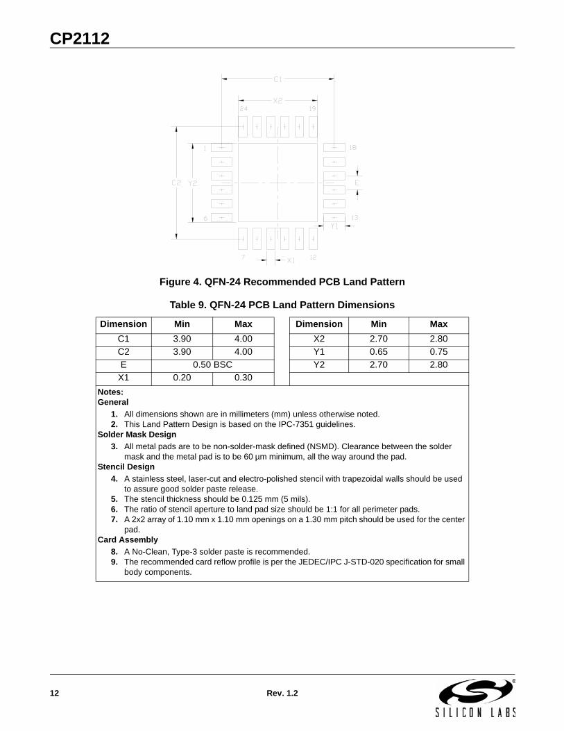
Figure 4. QFN-24 Recommended PCB Land Pattern
Table 9. QFN-24 PCB Land Pattern Dimensions
Dimension Min Max Dimension Min Max
C1 3.90 4.00 X2 2.70 2.80
C2 3.90 4.00 Y1 0.65 0.75
E 0.50 BSC Y2 2.70 2.80
X1 0.20 0.30
Notes:General
1. All dimensions shown are in millimeters (mm) unless otherwise noted.2. This Land Pattern Design is based on the IPC-7351 guidelines.
Solder Mask Design
3. All metal pads are to be non-solder-mask defined (NSMD). Clearance between the solder mask and the metal pad is to be 60 µm minimum, all the way around the pad.
Stencil Design
4. A stainless steel, laser-cut and electro-polished stencil with trapezoidal walls should be used to assure good solder paste release.
5. The stencil thickness should be 0.125 mm (5 mils).6. The ratio of stencil aperture to land pad size should be 1:1 for all perimeter pads.7. A 2x2 array of 1.10 mm x 1.10 mm openings on a 1.30 mm pitch should be used for the center
pad.Card Assembly
8. A No-Clean, Type-3 solder paste is recommended.9. The recommended card reflow profile is per the JEDEC/IPC J-STD-020 specification for small
body components.
12 Rev. 1.2

CP2112
5. USB Function Controller and Transceiver
The Universal Serial Bus (USB) function controller in the CP2112 is a USB 2.0 compliant full-speed device withintegrated transceiver and on-chip matching and pullup resistors. The USB function controller manages all datatransfers between the USB and the SMBus interface as well as command requests generated by the USB hostcontroller and commands for controlling the function of the SMBus interface and GPIO pins.
The USB Suspend and Resume modes are supported for power management of both the CP2112 device andexternal circuitry. The CP2112 enters Suspend mode when Suspend signaling is detected on the bus. Uponentering Suspend mode, the Suspend signals are asserted. The Suspend signals are also asserted after a CP2112reset until device configuration during USB enumeration is complete. SUSPEND is logic high when the device is inthe Suspend state and logic low when the device is in normal mode. The SUSPEND pin has the opposite logicvalue of the SUSPEND pin.
The CP2112 exits Suspend mode when any of the following events occur: Resume signaling is detected orgenerated, a USB Reset signal is detected, or a device reset occurs. SUSPEND and SUSPEND are weakly pulledto VIO in a high-impedance state during a CP2112 reset. If this behavior is undesirable, a strong pulldown resistor(10 k) can be used to ensure SUSPEND remains low during reset. The eight GPIO pins will retain their stateduring Suspend mode.
6. System Management Bus (SMBus) Interface
The SMBus I/O interface is a two-wire, bidirectional serial bus. The SMBus is compliant with the SystemManagement Bus Specification, Version 1.1, and compatible with the I2C serial bus. Reads and writes to theinterface by the system controller are byte-oriented with the SMBus interface autonomously controlling the serialtransfer of the data. The CP2112 operates as an SMBus master; however, it has an SMBus slave address that isconfigurable. The CP2112 will only ACK this address and will not respond to any read or write requests. If the leastsignificant bit of the address is set, the device will ignore it.
6.1. SMBus ConfigurationFigure 5 shows a typical SMBus configuration. The SMBus specification allows any recessive voltage between3.0 V and 5.0 V; different devices on the bus may operate at different voltage levels. The bidirectional serial clock(SCL) and serial data (SDA) lines must be connected to a positive power supply voltage through a pullup resistor orsimilar circuit. Every device connected to the bus must have an open-drain or open-collector output for both theSCL and SDA lines so that both are pulled high (recessive state) when the bus is free. The maximum number ofdevices on the bus is limited only by the requirement that the rise and fall times on the bus not exceed 300 ns and1000 ns, respectively. The SMBus provides control of SDA, SCL generation and synchronization, arbitration logic,and START/STOP control and generation.
Figure 5. Typical SMBus Configuration
VDD = 5 V
CP2112(Master Device)
Slave Device 1
Slave Device 2
VDD = 3 V VDD = 5 V VDD = 3 V
SDA
SCL
Rev. 1.2 13
CP2112
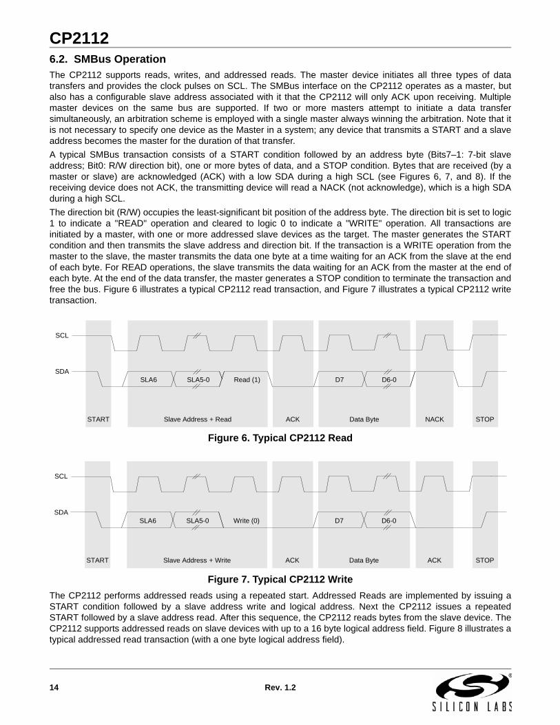
6.2. SMBus OperationThe CP2112 supports reads, writes, and addressed reads. The master device initiates all three types of datatransfers and provides the clock pulses on SCL. The SMBus interface on the CP2112 operates as a master, butalso has a configurable slave address associated with it that the CP2112 will only ACK upon receiving. Multiplemaster devices on the same bus are supported. If two or more masters attempt to initiate a data transfersimultaneously, an arbitration scheme is employed with a single master always winning the arbitration. Note that itis not necessary to specify one device as the Master in a system; any device that transmits a START and a slaveaddress becomes the master for the duration of that transfer.A typical SMBus transaction consists of a START condition followed by an address byte (Bits7–1: 7-bit slaveaddress; Bit0: R/W direction bit), one or more bytes of data, and a STOP condition. Bytes that are received (by amaster or slave) are acknowledged (ACK) with a low SDA during a high SCL (see Figures 6, 7, and 8). If thereceiving device does not ACK, the transmitting device will read a NACK (not acknowledge), which is a high SDAduring a high SCL.
The direction bit (R/W) occupies the least-significant bit position of the address byte. The direction bit is set to logic1 to indicate a "READ" operation and cleared to logic 0 to indicate a "WRITE" operation. All transactions areinitiated by a master, with one or more addressed slave devices as the target. The master generates the STARTcondition and then transmits the slave address and direction bit. If the transaction is a WRITE operation from themaster to the slave, the master transmits the data one byte at a time waiting for an ACK from the slave at the endof each byte. For READ operations, the slave transmits the data waiting for an ACK from the master at the end ofeach byte. At the end of the data transfer, the master generates a STOP condition to terminate the transaction andfree the bus. Figure 6 illustrates a typical CP2112 read transaction, and Figure 7 illustrates a typical CP2112 writetransaction.
Figure 6. Typical CP2112 Read
Figure 7. Typical CP2112 Write
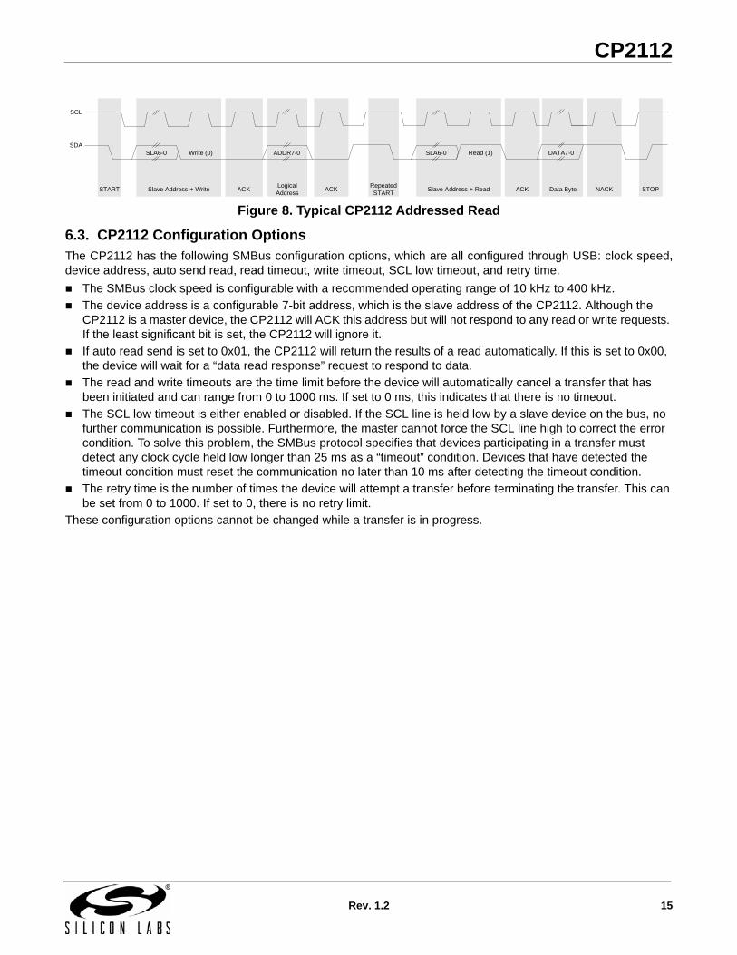
The CP2112 performs addressed reads using a repeated start. Addressed Reads are implemented by issuing aSTART condition followed by a slave address write and logical address. Next the CP2112 issues a repeatedSTART followed by a slave address read. After this sequence, the CP2112 reads bytes from the slave device. TheCP2112 supports addressed reads on slave devices with up to a 16 byte logical address field. Figure 8 illustrates atypical addressed read transaction (with a one byte logical address field).
SLA6SDA
SLA5-0 Read (1) D7 D6-0
Slave Address + Read Data ByteSTART ACK NACK STOP
SCL
SLA6SDA
SLA5-0 Write (0) D7 D6-0
SCL
Slave Address + Write Data ByteSTART ACK ACK STOP
14 Rev. 1.2
CP2112
Figure 8. Typical CP2112 Addressed Read
6.3. CP2112 Configuration OptionsThe CP2112 has the following SMBus configuration options, which are all configured through USB: clock speed,device address, auto send read, read timeout, write timeout, SCL low timeout, and retry time.
The SMBus clock speed is configurable with a recommended operating range of 10 kHz to 400 kHz.
The device address is a configurable 7-bit address, which is the slave address of the CP2112. Although the CP2112 is a master device, the CP2112 will ACK this address but will not respond to any read or write requests. If the least significant bit is set, the CP2112 will ignore it.
If auto read send is set to 0x01, the CP2112 will return the results of a read automatically. If this is set to 0x00, the device will wait for a “data read response” request to respond to data.
The read and write timeouts are the time limit before the device will automatically cancel a transfer that has been initiated and can range from 0 to 1000 ms. If set to 0 ms, this indicates that there is no timeout.
The SCL low timeout is either enabled or disabled. If the SCL line is held low by a slave device on the bus, no further communication is possible. Furthermore, the master cannot force the SCL line high to correct the error condition. To solve this problem, the SMBus protocol specifies that devices participating in a transfer must detect any clock cycle held low longer than 25 ms as a “timeout” condition. Devices that have detected the timeout condition must reset the communication no later than 10 ms after detecting the timeout condition.
The retry time is the number of times the device will attempt a transfer before terminating the transfer. This can be set from 0 to 1000. If set to 0, there is no retry limit.
These configuration options cannot be changed while a transfer is in progress.
RepeatedSTART
Read (1)
Slave Address + Read
SLA6-0SDA
Write (0) ADDR7-0
SCL
Slave Address + Write Data ByteSTART ACK ACKACKLogical Address
SLA6-0 DATA7-0
NACK STOP
Rev. 1.2 15

CP2112
7. GPIO Pins
The CP2112 supports 8 user-configurable GPIO pins. Each of these GPIO pins are usable as inputs, open-drainoutputs, or push-pull outputs. Three of these GPIO pins also have alternate functions which are listed in Table 10.
By default, all of the GPIO pins are configured as a GPIO input. The pins must be configured each time the deviceis reset. For example, if a device is unplugged and then plugged into a PC, the GPIO pins would be configured asinputs and would need to be reconfigured as needed.
The difference between an open-drain output and a push-pull output is when the GPIO output is driven to logichigh. A logic high, open-drain output pulls the pin to the VIO rail through an internal, pull-up resistor. A logic high,push-pull output directly connects the pin to the VIO voltage. Open-drain outputs are typically used wheninterfacing to logic at a higher voltage than the VIO pin. These pins can be safely pulled to the higher, externalvoltage through an external pull-up resistor. The maximum external pull-up voltage is 5 V.
The speed of reading and writing the GPIO pins is subject to the timing of the USB bus. GPIO pins configured asinputs or outputs are not recommended for real-time signaling.
7.1. GPIO.0-1—Transmit and Receive ToggleGPIO.0 and GPIO.1 are configurable as Transmit Toggle and Receive Toggle pins. These pins are logic high whena device is not transmitting or receiving data, and they toggle at a fixed rate as specified in Table 6 on page 7 whendata transfer is in progress. Typically, these pins are connected to two LEDs to indicate data transfer.
Figure 9. Transmit and Receive Toggle Typical Connection Diagram
7.2. GPIO.7—Clock OutputGPIO.7 is configurable to output a configurable CMOS clock output. The clock output appears at the pin at thesame time the device completes enumeration and exits USB Suspend mode. The clock output is removed from thepin when the device enters USB Suspend mode. The output frequency is configurable through the use of a dividerand the accuracy is specified in Table 6. When the divider is set to 0, the output frequency is 48 MHz. For dividervalues between 1 and 255, the output frequency is determined by the formula:
Equation 1. GPIO.7 Clock Output Frequency
Table 10. GPIO Pin Alternate Functions
GPIO Pin Alternate Function
GPIO.0 TX Toggle
GPIO.1 RX Toggle
GPIO.7 CLK Output
CP2112
GPIO.0 – TX Toggle
GPIO.1 – RX Toggle
VIO
GPIO.7 Clock Frequency48 MHz
2 ClockDivider-----------------------------------------------=
16 Rev. 1.2

CP2112
8. One-Time Programmable ROM
The CP2112 includes an internal, one-time programmable ROM that may be used to customize the USB vendor ID(VID), product ID (PID), manufacturer string, product description string, power descriptor, device release number,and device serial number as desired for OEM applications. If the programmable ROM has not been customized,the default configuration data shown in Table 11 is used.
While customization of the USB configuration data is optional, customizing the VID/PID combination is stronglyrecommended. A unique VID/PID will prevent the device from being recognized by any other manufacturer’ssoftware application. A vendor ID can be obtained from www.usb.org, or Silicon Labs can provide a free PID for theOEM product that can be used with the Silicon Labs VID. Customizing the serial string for each individual device isalso recommended if the OEM application is one in which it is possible for multiple CP2112-based devices to beconnected to the same PC.
“AN495: CP2112 Interface Specification” includes more information about the programmable values and their validoptions. Note that certain items in the PROM are programmed as a group, and programming one of these items ina group prevents further programming of any of the other items in the group.
The configuration data ROM is programmable by Silicon Labs prior to shipment with the desired configurationinformation. It can also be programmed in-system over the USB interface by adding a capacitor to the PCB. Ifconfiguration ROM is to be programmed in-system, a 4.7 µF capacitor must be added between the VPP pin andground. No other circuitry should be connected to VPP during a programming operation, and VDD must remain at3.3 V or higher to successfully write to the configuration ROM.
Table 11. Default USB Configuration Data
Name Value
Vendor ID 10C4h
Product ID EA90h
Power Descriptor (Attributes) 80h (Bus-powered)
Power Descriptor (Max. Power) 32h (100 mA)
Release Number 0100h (Release Version 01.00)
Manufacturer String “Silicon Laboratories” (30 ASCII characters maximum)
Product Description String “CP2112 HID USB-to-SMBus Bridge” (30 ASCII characters maximum)
Serial String Unique 8-character ASCII string (30 ASCII characters maximum)
Rev. 1.2 17
CP2112
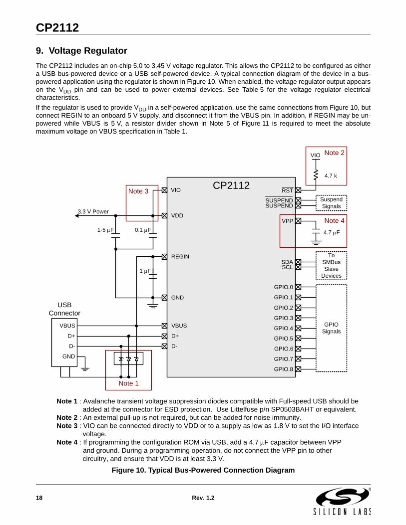
9. Voltage Regulator
The CP2112 includes an on-chip 5.0 to 3.45 V voltage regulator. This allows the CP2112 to be configured as eithera USB bus-powered device or a USB self-powered device. A typical connection diagram of the device in a bus-powered application using the regulator is shown in Figure 10. When enabled, the voltage regulator output appearson the VDD pin and can be used to power external devices. See Table 5 for the voltage regulator electricalcharacteristics.
If the regulator is used to provide VDD in a self-powered application, use the same connections from Figure 10, butconnect REGIN to an onboard 5 V supply, and disconnect it from the VBUS pin. In addition, if REGIN may be un-powered while VBUS is 5 V, a resistor divider shown in Note 5 of Figure 11 is required to meet the absolutemaximum voltage on VBUS specification in Table 1.
Figure 10. Typical Bus-Powered Connection Diagram
Note 2
Note 1
VBUS
D+
D-
GND
USB Connector
SuspendSignals
GPIO Signals
CP2112
GPIO.0
GPIO.1
GPIO.2
GPIO.3
VPP
SUSPENDSUSPEND
GPIO.4
GPIO.5
GPIO.8
GPIO.6
GPIO.7
VBUS
D+
D-
RST
VIO
4.7 k
Note 4
Note 1 : Avalanche transient voltage suppression diodes compatible with Full-speed USB should be added at the connector for ESD protection. Use Littelfuse p/n SP0503BAHT or equivalent.
Note 2 : An external pull-up is not required, but can be added for noise immunity.Note 3 : VIO can be connected directly to VDD or to a supply as low as 1.8 V to set the I/O interface
voltage.Note 4 : If programming the configuration ROM via USB, add a 4.7 F capacitor between VPP and ground. During a programming operation, do not connect the VPP pin to other
circuitry, and ensure that VDD is at least 3.3 V.
4.7 F
Note 3
REGIN
VDD
GND
VIO
1 F
1-5 F 0.1 F
3.3 V Power
To SMBus Slave
Devices
SDASCL
18 Rev. 1.2

CP2112
Alternatively, if 3.0 to 3.6 V power is supplied to the VDD pin, the CP2112 can function as a USB self-powereddevice with the voltage regulator bypassed. For this configuration, tie the REGIN input to VDD to bypass the voltageregulator. A typical connection diagram showing the device in a self-powered application with the regulatorbypassed is shown in Figure 11.
The USB max power and power attributes descriptor must match the device power usage and configuration. Seethe CP2112_SetIDs software included with the CP2112 Software Development Kit (SDK) for information on how tocustomize USB descriptors for the CP2112.
Figure 11. Typical Self-Powered Connection Diagram (Regulator Bypass)
Note 3
Note 2
Note 1
VBUS
D+
D-
GND
USB Connector
SuspendSignals
GPIO Signals
CP2112
GPIO.0
GPIO.1
GPIO.2
GPIO.3
VPP
SUSPENDSUSPEND
GPIO.4
GPIO.5
GPIO.8
GPIO.6
GPIO.7
VDD
REGIN
GND
VIO
VBUS
D+
D-
RST
0.1 F1-5 F
VIO
4.7 k
Note 4
Note 1 : Avalanche transient voltage suppression diodes compatible with Full-speed USB should be added at the connector for ESD protection. Use Littelfuse p/n SP0503BAHT or equivalent.
Note 2 : An external pull-up is not required, but can be added for noise immunity.Note 3 : VIO can be connected directly to VDD or to a supply as low as 1.8 V to set the I/O interface
voltage.Note 4 : If programming the configuration ROM via USB, add a 4.7 F capacitor between VPP and ground. During a programming operation, do not connect the VPP pin to other
circuitry, and ensure that VDD is at least 3.3 V.Note 5 : For self-powered systems where VDD and VIO may be unpowered when VBUS is connected to 5 V, a resistor divider (or functionally-equivalent circuit) on VBUS is required to meet the absolute maximum voltage on VBUS specification in the Electrical Characteristics section.
4.7 F
3.3 VPower
To SMBus Slave
Devices
SDASCL
47 k
24 kNote 5(Optional)
Rev. 1.2 19
CP2112
10. CP2112 Interface Specification and Windows Interface DLL
The CP2112 is a USB Human Interface Device (HID), and, since most operating systems include native drivers,custom drivers do not need to be installed. Because the CP2112 does not fit a standard HID device type, such as akeyboard or mouse, any CP2112 PC application needs to use the CP2112’s HID specification to communicate withthe device. The low-level HID specification for the CP2112 is provided in “AN495: CP2112 Interface Specification”.This document describes all of the basic functions for opening, reading from, writing to, and closing the device, aswell as the ROM programming functions.
A Windows DLL that encapsulates the CP2112 HID interface and also adds higher level features, such as read/write timeouts is provided by Silicon Labs. This DLL is the recommended interface for the CP2112. The WindowsDLL is documented in CP2112 Windows DLL Specification.
Both of these documents and the DLL are available in the CP2112EK CD as well as online at www.silabs.com.
11. Relevant Application Notes and Software
The following Application Notes are applicable to the CP2112. The latest versions of these application notes andtheir accompanying software are available at www.silabs.com/interface-appnotes.
AN495: CP2112 Interface Specification—describes how to interface to the CP2112 using the low-level, HID Interface.
AN496: CP2112 HID USB-to-SMBus API Specification—describes how to interface to the CP2112 using the Windows Interface DLL.
The CP2112 Software Development Kit can be downloaded from www.silabs.com/interface-software. See theCP2112_SetIDs software included with the CP2112 Software Development Kit (SDK) for information on how tocustomize USB descriptors for the CP2112.
12. Device Specific Behavior
This section describes differences in behavior between the CP2112-F01-GM and the CP2112-F02-GM. Therevision of the CP2112 can be read by using the Get Version Information command (Report ID 0x05) or byconnecting to a CP2112 device using the HidSmbus Example application. The part number will always be 0x0C(specifying the CP2112 as the device) and the device version will be the revision of the device.
12.1. Addressed Read RequestsIn F01 devices, addressed read requests are performed by issuing a start on the bus, followed by a slave address(write), logical address to read, stop, start, and slave address (read).
F02 devices handle addressed read requests by issuing a start on the bus, followed by a slave address (write),logical address to read, repeated start, and slave address (read).
12.2. Multimaster ApplicationsF01 devices can hold the SDA line low for approximately 3 ms if the Set SMBus Configuration command (ReportID 0x06) is received by one CP2112 master during the middle of a separate master device's transaction. A fix isimplemented on F02 devices to eliminate this behavior.
20 Rev. 1.2

CP2112
DOCUMENT CHANGE LIST
Revision 0.1 to Revision 0.5 Updated Table 3 on page 6.
Updated Table 4 on page 6.
Updated Table 5 on page 6.
Updated Table 11 on page 17.
Revision 0.5 to Revision1.0 Removed preliminary language.
Revision 1.0 to Revision 1.1 Updated ordering part number.
Updated "6.2. SMBus Operation" on page 14 to describe SMBus transactions supported by CP2112.
Updated Figure 6 and added Figures 7 and 8.
Added "12. Device Specific Behavior" on page 20.
Revision 1.1 to Revision 1.2 Added a row for VBUS in Table 1, “Absolute
Maximum Ratings,” on page 5.
Added VDD Ramp Time for Power On specification to Table 4, “Reset Electrical Characteristics,” on page 6.
Added VPP Voltage and Capacitor specifications to Table 2, “Global DC Electrical Characteristics,” on page 5.
Removed AN144 references.
Added references to the CP2112_SetIDs software and CP2112 SDK.
Updated "9. Voltage Regulator" on page 18 to add absolute maximum voltage on VBUS requirements in self-powered systems.
Rev. 1.2 21
CP2112
CONTACT INFORMATIONSilicon Laboratories Inc.400 West Cesar ChavezAustin, TX 78701Tel: 1+(512) 416-8500Fax: 1+(512) 416-9669Toll Free: 1+(877) 444-3032
Please visit the Silicon Labs Technical Support web page:https://www.silabs.com/support/pages/contacttechnicalsupport.aspxand register to submit a technical support request.
Patent NoticeSilicon Labs invests in research and development to help our customers differentiate in the market with innovative low-power, small size, analog-intensive mixed-signal solutions. Silicon Labs' extensive patent portfolio is a testament to our unique approach and world-class engineering team.
Silicon Laboratories and Silicon Labs are trademarks of Silicon Laboratories Inc.Other products or brandnames mentioned herein are trademarks or registered trademarks of their respective holders.
The information in this document is believed to be accurate in all respects at the time of publication but is subject to change without notice. Silicon Laboratories assumes no responsibility for errors and omissions, and disclaims responsibility for any consequences resulting from the use of information included herein. Additionally, Silicon Laboratories assumes no responsibility for the functioning of undescribed features or parameters. Silicon Laboratories reserves the right to make changes without further notice. Silicon Laboratories makes no warranty, rep-resentation or guarantee regarding the suitability of its products for any particular purpose, nor does Silicon Laboratories assume any liability arising out of the application or use of any product or circuit, and specifically disclaims any and all liability, including without limitation conse-quential or incidental damages. Silicon Laboratories products are not designed, intended, or authorized for use in applications intended to support or sustain life, or for any other application in which the failure of the Silicon Laboratories product could create a situation where per-sonal injury or death may occur. Should Buyer purchase or use Silicon Laboratories products for any such unintended or unauthorized ap-plication, Buyer shall indemnify and hold Silicon Laboratories harmless against all claims and damages.
22 Rev. 1.2