Cover - NXP Semiconductorscache.freescale.com/files/dsp/doc/inactive/DSP56100FM.pdf · Order this...
477
DSP56100 16-BIT DIGITAL SIGNAL PROCESSOR FAMILY MANUAL Motorola, Inc. Semiconductor Products Sector DSP Division 6501 William Cannon Drive, West Austin, Texas 78735-8598 Freescale Semiconductor, I Freescale Semiconductor, Inc. For More Information On This Product, Go to: www.freescale.com nc...
Transcript of Cover - NXP Semiconductorscache.freescale.com/files/dsp/doc/inactive/DSP56100FM.pdf · Order this...
DSP56100
16-BITDIGITAL SIGNAL PROCESSOR
FAMILY MANUAL
Motorola, Inc.Semiconductor Products SectorDSP Division6501 William Cannon Drive, WestAustin, Texas 78735-8598
Fre
esc
ale
Se
mic
on
du
cto
r, I
Freescale Semiconductor, Inc.
For More Information On This Product, Go to: www.freescale.com
nc
...

Order this document by DSP56100FM/AD
Motorola reserves the right to make changes without further notice to any products herein to im-prove reliability, function or design. Motorola does not assume any liability arising out of the appli-cation or use of any product or circuit described herein; neither does it convey any license under itspatent rights nor the rights of others. Motorola products are not authorized for use as componentsin life support devices or systems intended for surgical implant into the body or intended to supportor sustain life. Buyer agrees to notify Motorola of any such intended end use whereupon Motorolashall determine availability and suitability of its product or products for the use intended. Motorolaand M are registered trademarks of Motorola, Inc. Motorola, Inc. is an Equal Employment Oppor-tunity /Affirmative Action Employer.
OnCE is a trade mark of Motorola, Inc.
Motorola Inc., 1994
Fre
esc
ale
Se
mic
on
du
cto
r, I
Freescale Semiconductor, Inc.
For More Information On This Product, Go to: www.freescale.com
nc
...

Fre
esc
ale
Se
mic
on
du
cto
r, I
Freescale Semiconductor, Inc.n
c..
.
SECTION 1
DSP56100 FAMILY INTRODUCTION
MOTOROLA DSP56100 FAMILY INTRODUCTION 1 - 1 For More Information On This Product,
Go to: www.freescale.com

SECTION CONTENTS
1 - 2
DSP56100 FAMILY INTRODUCTION
MOTOROLA
1.1 INTRODUCTION . . . . . . . . . . . . . . . . . . . . . . . . . . . . . . . . . . . . . . . . 1-31.2 DSP56100 FAMILY FEATURES . . . . . . . . . . . . . . . . . . . . . . . . . . . . 1-4
Fre
esc
ale
Se
mic
on
du
cto
r, I
Freescale Semiconductor, Inc.
For More Information On This Product, Go to: www.freescale.com
nc
...
INTRODUCTION
Fre
esc
ale
Se
mic
on
du
cto
r, I
Freescale Semiconductor, Inc.n
c..
.
1.1 INTRODUCTION
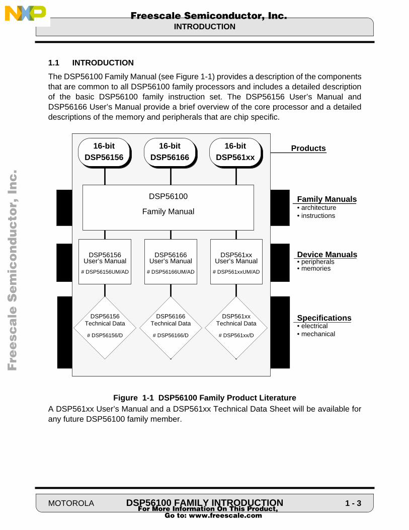
The DSP56100 Family Manual (see Figure 1-1) provides a description of the componentsthat are common to all DSP56100 family processors and includes a detailed descriptionof the basic DSP56100 family instruction set. The DSP56156 User’s Manual andDSP56166 User’s Manual provide a brief overview of the core processor and a detaileddescriptions of the memory and peripherals that are chip specific.
Figure 1-1 DSP56100 Family Product LiteratureA DSP561xx User’s Manual and a DSP561xx Technical Data Sheet will be available forany future DSP56100 family member.
Family Manuals• architecture• instructions
Device Manuals• peripherals• memories
Specifications • electrical• mechanical
Products
# DSP56166UM/AD
DSP56166User’s Manual
# DSP56156UM/AD
DSP56156User’s Manual
16-bitDSP56166
16-bitDSP56156
DSP56166Technical Data
# DSP56166/D
DSP56156Technical Data
# DSP56156/D
# DSP561xxUM/AD
DSP561xxUser’s Manual
16-bitDSP561xx
DSP561xxTechnical Data
# DSP561xx/D
DSP56100
Family Manual
MOTOROLA DSP56100 FAMILY INTRODUCTION 1 - 3 For More Information On This Product,
Go to: www.freescale.com

DSP56100 FAMILY FEATURES
Fre
esc
ale
Se
mic
on
du
cto
r, I
Freescale Semiconductor, Inc.n
c..
.
1.2 DSP56100 FAMILY FEATURES
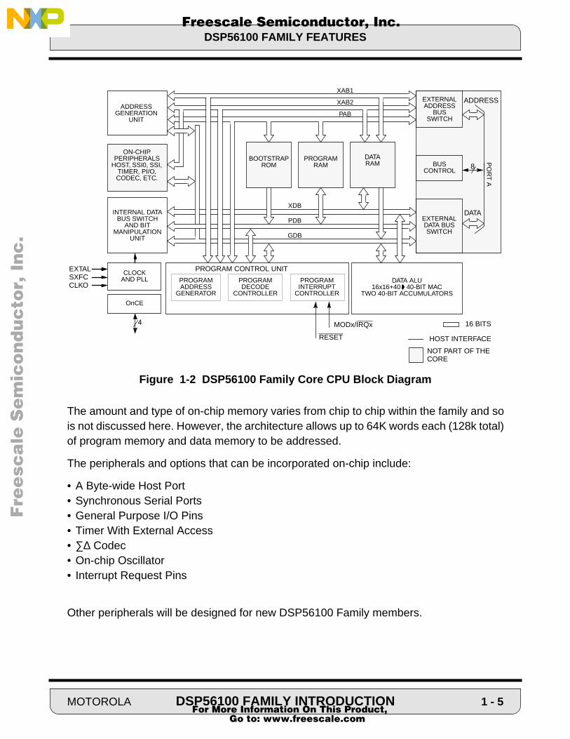
The DSP56100 family consists of programmable CMOS 16-bit Digital Signal Processorcore composed of a 16-bit arithmetic DATA ALU (DALU), Address Generation Unit(AGU), Program Controller Unit (PCU), and their associated DSP instruction set.
Table 1-1 gives a description of the DSP Core features.
Table 1-1 DSP Core Feature List
The block diagram of the core processor used in the DSP56100 family is shown in Figure1-2.
• Up to 30 Million Instructions per Second (MIPS) at 60 MHz.– 33.3 ns instruction cycle• Single-cycle 16 x 16-bit parallel multiply-accumulate• 2 x 40-bit accumulators with extension byte• Fractional and integer arithmetic with support for multiprecision arithmetic• Highly parallel instruction set with unique DSP addressing modes• Nested hardware DO loops including infinite loops• Two instruction LMS adaptive filter loop• Fast auto-return interrupts• Three external interrupt request pins• Three 16-bit internal data buses and three 16-bit internal address buses• Programmable access time on the external bus• On-chip peripheral registers memory mapped in data memory space• Off-chip peripheral space with programmable access time memory mapped in data memory space• Low power wait and stop modes• On-Chip Emulation (OnCE) for unobtrusive, processor speed independent debugging• Operating frequency down to DC• Single power supply• Low power (HCMOS)
1- 4 DSP56100 FAMILY INTRODUCTION MOTOROLA For More Information On This Product,
Go to: www.freescale.com
DSP56100 FAMILY FEATURES
Fre
esc
ale
Se
mic
on
du
cto
r, I
Freescale Semiconductor, Inc.n
c..
.
Figure 1-2 DSP56100 Family Core CPU Block Diagram
The amount and type of on-chip memory varies from chip to chip within the family and sois not discussed here. However, the architecture allows up to 64K words each (128k total)of program memory and data memory to be addressed.
The peripherals and options that can be incorporated on-chip include:
• A Byte-wide Host Port• Synchronous Serial Ports• General Purpose I/O Pins• Timer With External Access• ∑∆ Codec• On-chip Oscillator• Interrupt Request Pins
Other peripherals will be designed for new DSP56100 Family members.
XAB1
XAB2
PAB
XDB
PDB
GDB
4
ADDRESS
PO
RT
A
PROGRAM CONTROL UNIT
MODx/IRQx
ON-CHIPPERIPHERALS
HOST, SSI0, SSI, TIMER, PI/O, CODEC, ETC.
INTERNAL DATA BUS SWITCH
AND BITMANIPULATION
UNIT
EXTERNALADDRESS
BUSSWITCH
BUSCONTROL
EXTERNALDATA BUSSWITCH
BOOTSTRAPROM
PROGRAMRAM
DATARAM
PROGRAMADDRESS
GENERATOR
PROGRAMDECODE
CONTROLLER
PROGRAMINTERRUPT
CONTROLLER
DATA ALU16x16+40 - 40-BIT MAC
TWO 40-BIT ACCUMULATORS
CLOCKAND PLL
EXTAL
RESET
16 BITS
DATA
8
ADDRESSGENERATION
UNIT
OnCE
SXFCCLKO
HOST INTERFACE
NOT PART OF THE CORE
MOTOROLA DSP56100 FAMILY INTRODUCTION 1 - 5 For More Information On This Product,
Go to: www.freescale.com

DSP56100 FAMILY FEATURES
Fre
esc
ale
Se
mic
on
du
cto
r, I
Freescale Semiconductor, Inc.n
c..
.
1- 6 DSP56100 FAMILY INTRODUCTION MOTOROLA For More Information On This Product,
Go to: www.freescale.com

Fre
esc
ale
Se
mic
on
du
cto
r, I
Freescale Semiconductor, Inc.n
c..
.
SECTION 2
CPU ARCHITECTURE OVERVIEW
MOTOROLA CPU ARCHITECTURE OVERVIEW 2 - 1 For More Information On This Product,
Go to: www.freescale.com

SECTION CONTENTS
Fre
esc
ale
Se
mic
on
du
cto
r, I
Freescale Semiconductor, Inc.n
c..
.
2.1 INTRODUCTION . . . . . . . . . . . . . . . . . . . . . . . . . . . . . . . . . . . . . . . . 2-32.2 DSP56100 BLOCK DIAGRAM . . . . . . . . . . . . . . . . . . . . . . . . . . . . . . 2-32.2.1 Data Buses . . . . . . . . . . . . . . . . . . . . . . . . . . . . . . . . . . . . . . . . . . . . . 2-32.2.2 Address Buses . . . . . . . . . . . . . . . . . . . . . . . . . . . . . . . . . . . . . . . . . . 2-32.2.3 Internal Bus Switch . . . . . . . . . . . . . . . . . . . . . . . . . . . . . . . . . . . . . . . 2-42.2.4 Bit Manipulation Unit . . . . . . . . . . . . . . . . . . . . . . . . . . . . . . . . . . . . . . 2-42.2.5 Data ALU (DALU) . . . . . . . . . . . . . . . . . . . . . . . . . . . . . . . . . . . . . . . . 2-42.2.6 Address Generation Unit (AGU) . . . . . . . . . . . . . . . . . . . . . . . . . . . . . 2-42.2.7 X Data Memory . . . . . . . . . . . . . . . . . . . . . . . . . . . . . . . . . . . . . . . . . . 2-62.2.8 Program Memory . . . . . . . . . . . . . . . . . . . . . . . . . . . . . . . . . . . . . . . . 2-62.2.9 Bootstrap Memory . . . . . . . . . . . . . . . . . . . . . . . . . . . . . . . . . . . . . . . . 2-62.2.10 Program Control Unit (PCU) and System Stack (SS) . . . . . . . . . . . . . 2-62.2.11 External Bus Interface . . . . . . . . . . . . . . . . . . . . . . . . . . . . . . . . . . . . . 2-7
2 - 2 CPU ARCHITECTURE OVERVIEW MOTOROLA For More Information On This Product,
Go to: www.freescale.com

INTRODUCTION
Fre
esc
ale
Se
mic
on
du
cto
r, I
Freescale Semiconductor, Inc.n
c..
.
2.1 INTRODUCTIONThe heart of the DSP56100 architecture is a 16-bit multiple-bus processor designed spe-cifically for real-time digital signal processing (DSP). The overall architecture is presentedand detailed block diagrams of the Data ALU and Address ALU architecture are de-scribed.
2.2 DSP56100 BLOCK DIAGRAMThe major components of the CPU are:
• Data Buses• Address Buses• Data ALU• Address ALU• Program Control and System Stack
An overall block diagram of the CPU architecture is shown in Figure 2-1.
2.2.1 Data BusesData movement on the chip occurs over three bidirectional 16-bit buses: the X Data Bus(XDB), the Program Data Bus (PDB), and the Global Data Bus (GDB). Data transfer be-tween the Data ALU and the X Data Memory occurs over the XDB when one memory ac-cess is performed, over the XDB and the GDB when two simultaneous memory reads areperformed. All other data transfers occur over the GDB. Instruction word pre-fetches takeplace in parallel over the PDB. The bus structure supports general register to register, reg-ister to memory, memory to register, and memory to memory data movement and cantransfer up to three 16-bit words in the same instruction cycle. Transfers between busesare accomplished through the Internal Bus Switch.
As a general rule, when reading any 8-bit register, the unused bits in the most significantbyte are zero filled and any unused or reserved bits are read as zero.
2.2.2 Address BusesAddresses are specified for internal X Data Memory on two unidirectional 16-bit buses, XAddress Bus One (XAB1) and X Address Bus Two (XAB2). Program memory addressesare specified on the bidirectional Program Address Bus (PAB).
When external memory spaces have to be addressed, a single 16-bit unidirectional ad-dress bus driven by a three input multiplexer can select: XAB1, XAB2, or the PAB. Oneinstruction cycle is needed for each external memory access. There is no speed penaltyif only one external memory space is accessed in an instruction and if no wait states are
MOTOROLA CPU ARCHITECTURE OVERVIEW 2 - 3 For More Information On This Product,
Go to: www.freescale.com

DSP56100 BLOCK DIAGRAM
Fre
esc
ale
Se
mic
on
du
cto
r, I
Freescale Semiconductor, Inc.n
c..
.
inserted in the external bus cycle. If two or three external memory spaces are accessedin a single instruction, there will be a one or two instruction cycle execution delay, respec-tively, or more if wait states are inserted on the external bus. A bus arbitrator controls ex-ternal accesses, making it transparent to the user.
2.2.3 Internal Bus SwitchTransfers between buses are accomplished in the Internal Bus Switch. The internal busswitch is similar to a switch matrix and can connect any two internal buses without addingany pipeline delays.
2.2.4 Bit Manipulation UnitThe bit manipulation unit performs bit manipulation and bit field manipulation on memorywords and register data. It is capable of testing and/or changing a user selected set of bitswithin a byte.
2.2.5 Data ALU (DALU)The Data ALU performs all of the arithmetic and logical operations on data operands. TheData ALU consists of four 16-bit input registers, two 32-bit accumulator registers, two 8-bit accumulator extension registers, an accumulator shifter, an output shifter, one databus shifter/limiter, and a parallel single cycle non-pipelined Multiply-Accumulator (MAC)unit. Data ALU registers may be read or written by the XDB and GDB as 16-bit operands.The Data ALU is capable of multiplication, multiply-accumulate with positive or negativeaccumulation, addition, subtraction, shifting, and logical operations in one instruction cy-cle. Data ALU arithmetic operations generally use fractional 2’s complement arithmetic.Some signed/unsigned and integer operations are also possible. Data ALU source oper-ands may be 16, 32 or 40 bits and may originate from input registers and/or accumulators.ALU results are always stored in one of the accumulators. The upper 16-bits of an accu-mulator can be used as a multiplier input. Arithmetic operations always have a 40-bit re-sult and logical operations are performed on 16-bit operands yielding 16-bit results in oneof the two accumulators. Refer to Section 3 for a detailed description of the Data ALU ar-chitecture.
2.2.6 Address Generation Unit (AGU)The AGU performs all address storage and effective address calculations necessary toaddress data operands in memory. This unit operates in parallel with other chip resourcesto minimize address generation overhead. The AGU can implement three types of arith-metic: linear, modulo, and reverse carry. The Address ALU contains four Address Regis-ters (R0-R3), four Offset Registers (N0-N3), and four Modifier Registers (M0-M3). The
2 - 4 CPU ARCHITECTURE OVERVIEW MOTOROLA For More Information On This Product,
Go to: www.freescale.com

DSP56100 BLOCK DIAGRAM
Fre
esc
ale
Se
mic
on
du
cto
r, I
Freescale Semiconductor, Inc.n
c..
.
Address Registers are 16-bit registers which may contain address or data. Each AddressRegister may be output to the PAB and XAB1. R3 may be accessed for output to XAB2
16
ON-CHIP I/O
PERIPHERALS
ON-CHIPMEMORY
ON-CHIP I/O
PERIPHERALS
ON-CHIPMEMORY
SSH SSL
31 00
15
SP
6 0
PROGRAMCONTROL
UNIT
LA LC
PC MR CCR OMR
15 0 15 0
15 015 0
m0m1m2
n0n1n2
r0r1r2
m3 n3 r3
ALU
ADDRESS GENERATION UNIT
OnCE
INT. DATA BUS SWITCHAND BIT MANIPULATION
DATAALUSHIFTER/LIMITER
X1 X0 Y1 Y0 A2 A1 A0 B2 B1 B0
COND. GEN.
AC
CU
SH
IFT
ER
MR
16 x 16 → 40 BIT MAC ALU
control bus
SH
IFT
ER
XAB1
XAB2
PAB
XDB
PDB
GDB
16
16
16
16
16
16
16
16
8
1616
8
GDB
SR
Figure 2-1 Architecture of the 16-Bit DSP CPU
MOTOROLA CPU ARCHITECTURE OVERVIEW 2 - 5 For More Information On This Product,
Go to: www.freescale.com

DSP56100 BLOCK DIAGRAM
Fre
esc
ale
Se
mic
on
du
cto
r, I
Freescale Semiconductor, Inc.n
c..
.
when R0, R1, or R2 are output to XAB1. The modifier and offset registers are 16-bit reg-isters which are normally used to control updating of the address registers. Offset regis-ters can also be used as 16-bit data general purpose registers.
AGU registers may be read or written by the GDB as 16-bit operands. The AGU can gen-erate two 16-bit addresses every instruction cycle: one for either the XAB1 or PAB andone for XAB2. The ALU can directly address 65536 locations on the XAB and 65536 lo-cations on the XAB2 bus - a total capability of 131,072 16-bit data words. Refer to Section4 for a detailed description of the AGU architecture.
2.2.7 X Data MemoryThe On-Chip X Data Memory addresses are received from the XAB1 and XAB2 and datatransfers occur on the XDB and GDB. Two reads or one write can be performed duringone instruction cycle on the internal data memory. The on-chip peripherals occupy the top64 locations in the X data memory space (X:$FFC0-X:$FFFF). X memory may be expand-ed off-chip for a total of 65,536 addressable locations.
2.2.8 Program MemoryThe On-Chip Program Memory addresses are received from the program control logic(usually the program counter) or from the address ALU on the PAB. The first 64 locationsof the program memory are reserved for interrupt vectors. The program memory may beexpanded off-chip for a total of 65,536 addressable locations.
2.2.9 Bootstrap MemoryA program bootstrap ROM is only read by the program controller while in the bootstrapmode, during which, the on-chip program RAM is defined as write-only.
2.2.10 Program Control Unit (PCU) and System Stack (SS)The Program Control Unit performs instruction prefetch, instruction decoding, hardwareloop control and exception processing. It contains six, 16-bit directly addressable regis-ters. They are the:
1. Program Counter (PC),
2. Loop Address (LA),
3. Loop Count (LC),
4. Status Register (SR),
5. Operating Mode Register (OMR),
6. Stack Pointer (SP).
2 - 6 CPU ARCHITECTURE OVERVIEW MOTOROLA For More Information On This Product,
Go to: www.freescale.com

DSP56100 BLOCK DIAGRAM
Fre
esc
ale
Se
mic
on
du
cto
r, I
Freescale Semiconductor, Inc.n
c..
.
The System Stack is a separate internal RAM 15 locations “deep” which stores the PCand the SR for subroutine calls and long interrupts. The stack will also store the LC andthe LA in addition to the PC and SR registers for program looping.
2.2.11 External Bus InterfaceA common address bus is used to access external Data Memory, Program Memory, orI/O devices when required. Separate select lines control access to the memory spaces.
MOTOROLA CPU ARCHITECTURE OVERVIEW 2 - 7 For More Information On This Product,
Go to: www.freescale.com

DSP56100 BLOCK DIAGRAM
Fre
esc
ale
Se
mic
on
du
cto
r, I
Freescale Semiconductor, Inc.n
c..
.
2 - 8 CPU ARCHITECTURE OVERVIEW MOTOROLA For More Information On This Product,
Go to: www.freescale.com

Fre
esc
ale
Se
mic
on
du
cto
r, I
Freescale Semiconductor, Inc.n
c..
.
SECTION 3
DATA ALU
MOTOROLA DATA ALU 3 - 1 For More Information On This Product,
Go to: www.freescale.com

SECTION CONTENTS
Fre
esc
ale
Se
mic
on
du
cto
r, I
Freescale Semiconductor, Inc.n
c..
.
3.1 OVERVIEW AND ARCHITECTURE . . . . . . . . . . . . . . . . . . . . . . . . . . 3-33.1.1 Data ALU Input Registers (X1, X0, Y1, Y0) . . . . . . . . . . . . . . . . . . . . 3-43.1.2 Data ALU Accumulator Registers (A2, A1, A0, B2, B1, B0) . . . . . . . . 3-43.1.3 Multiply-Accumulator (MAC) and Logic Unit . . . . . . . . . . . . . . . . . . . . 3-63.1.3.1 Multiply-Accumulator (MAC) Array and Logic unit . . . . . . . . . . . . . . . 3-73.1.3.2 ZB Multiplexer . . . . . . . . . . . . . . . . . . . . . . . . . . . . . . . . . . . . . . . . . . . 3-73.1.3.3 Multiplier Control Recoder (REC) . . . . . . . . . . . . . . . . . . . . . . . . . . . . 3-83.1.3.4 Extension Adder (EXA) . . . . . . . . . . . . . . . . . . . . . . . . . . . . . . . . . . . . 3-83.1.4 Accumulator Shifter (AS) . . . . . . . . . . . . . . . . . . . . . . . . . . . . . . . . . . 3-83.1.5 Output Shifter (OS) . . . . . . . . . . . . . . . . . . . . . . . . . . . . . . . . . . . . . . . 3-93.1.6 Data Shifter/Limiter . . . . . . . . . . . . . . . . . . . . . . . . . . . . . . . . . . . . . . . 3-93.1.6.1 Scaling . . . . . . . . . . . . . . . . . . . . . . . . . . . . . . . . . . . . . . . . . . . . . . . . 3-93.1.6.2 Limiting . . . . . . . . . . . . . . . . . . . . . . . . . . . . . . . . . . . . . . . . . . . . . . . . 3-93.2 THE DATA ALU ARITHMETIC AND ROUNDING . . . . . . . . . . . . . . . 3-103.2.1 Data Representation . . . . . . . . . . . . . . . . . . . . . . . . . . . . . . . . . . . . . . 3-103.2.2 Fractional Arithmetic . . . . . . . . . . . . . . . . . . . . . . . . . . . . . . . . . . . . . . 3-113.2.3 Integer Arithmetic . . . . . . . . . . . . . . . . . . . . . . . . . . . . . . . . . . . . . . . . 3-123.2.4 Multiprecision Arithmetic Support . . . . . . . . . . . . . . . . . . . . . . . . . . . . 3-143.2.5 Rounding Modes . . . . . . . . . . . . . . . . . . . . . . . . . . . . . . . . . . . . . . . . . 3-153.2.5.1 Convergent Rounding . . . . . . . . . . . . . . . . . . . . . . . . . . . . . . . . . . . . . 3-153.2.5.2 Two’s Complement Rounding . . . . . . . . . . . . . . . . . . . . . . . . . . . . . . . 3-18
3 - 2 DATA ALU MOTOROLA For More Information On This Product,
Go to: www.freescale.com

OVERVIEW AND ARCHITECTURE
Fre
esc
ale
Se
mic
on
du
cto
r, I
Freescale Semiconductor, Inc.n
c..
.
3.1 OVERVIEW AND ARCHITECTURE
This Section describes the structure and the operation of the Data ALU registers andhardware in addition to describing the data representation, rounding, and saturationarithmetic used within the Data ALU.
The major components of the Data ALU are
• Data ALU Input Registers• Data ALU Accumulator Registers• A parallel single cycle non-pipelined Multiply-Accumulator (MAC) Unit• An Accumulator Shifter (AS)• An Output Shifter (OS)• A Data Shifter/Limiter (S/L)
A block diagram of the Data ALU architecture is shown in Figure 3-1 and a functionalblock diagram is shown in Figure 3-2.
Figure 3-1 Data ALU Architecture Block Diagram
8
LSP(0:15)MSP(0:15)EXT(0:7)
EXA(0:7)
MSA(0:15)
X1 X0 Y1 Y0 A2 A1 A0 B2 B1 B0
CONDITIONGENERATOR
AC
CU
SH
IFT
ER
MR
MULTIPLY - ACCUMULATOR
AND LOGIC
OU
TP
UT
SH
IFT
ER
(O
S)
LSA(0:15)
ZB
(0:1
5)
ZB
(0:1
5)
MUX
MUX
NON MULTIPLYCONTROL
SB(0:15)
S/L
XD(0:15)
L
GD(0:15)
DXB2(0:15)
DXB1(0:15)
8
15
15
16
16
MOTOROLA DATA ALU 3 - 3 For More Information On This Product,
Go to: www.freescale.com

OVERVIEW AND ARCHITECTURE
Fre
esc
ale
Se
mic
on
du
cto
r, I
Freescale Semiconductor, Inc.n
c..
.
3.1.1 Data ALU Input Registers (X1, X0, Y1, Y0)
X1, X0, Y1, and Y0 are 16-bit latches which serve as input registers for the data ALU.Each register may be read or written by the XDB as well as the GDB. X0, X1, Y0, and Y1may be read over the XDB. They may be treated as four independent 16-bit registers oras two 32-bit registers called X and Y which are developed by concatenating X1:X0 andY1:Y0 respectively (where X1 and Y1 are the most significant words and X0 and Y0 arethe least significant words in X and Y respectively).
These Data ALU input registers are used as source operands for most data ALU opera-tions and allow new operands to be loaded for the next instruction while the register con-tents are used by the current instruction.
3.1.2 Data ALU Accumulator Registers (A2, A1, A0, B2, B1, B0)
A1, A0, B1 and B0 are 16-bit latches which serve as data ALU accumulator registers. A2and B2 are 8-bit latches which serve as accumulator extension registers. Each registermay be read or written by the XDB as a word operand. A1 and B1 may be read or writtenby the GDB. When A2 or B2 is read, the register contents occupy the low-order portion(bits 7-0) of the word; the high-order portion (bits 16-8) is sign-extended. When A2 or B2is written, the register receives the low-order portion of the word; the high-order portion isnot used.
The accumulator registers are treated as two 40-bit registers A (A2:A1:A0) and B(B2:B1:B0) for data ALU operations. These accumulator registers receive theEXT:MSP:LSP portion of the Multiply-Accumulator unit output and supply a source accu-mulator of the same form. Most data ALU operations specify the 40-bit accumulator reg-isters as source and/or destination operands
The accumulator registers are treated as two 40-bit registers A (A2:A1:A0) and B(B2:B1:B0) for data ALU operations. These accumulator registers receive theEXT:MSP:LSP portion of the Multiply-Accumulator unit output and supply a source accu-mulator of the same form. Most data ALU operations specify the 40-bit accumulator reg-isters as source and/or destination operands.
When one accumulator is used as a multiplier input, only the upper portion (A1 or B1)can be specified. This upper portion can also be directly used as an address register forfast effective address computation.
Automatic sign extension of the 40-bit accumulators is provided when the A or B registeris written with a smaller size operand. This can occur when writing A or B from the X databus or with the results of certain data ALU operations (such as Tcc or TFR). If a wordoperand is to be written to an accumulator register (A or B), the MSP portion of the accu-
3 - 4 DATA ALU MOTOROLA For More Information On This Product,
Go to: www.freescale.com

OVERVIEW AND ARCHITECTURE
Fre
esc
ale
Se
mic
on
du
cto
r, I
Freescale Semiconductor, Inc.n
c..
.
mulator is written with the word operand, the LSP portion is zeroed and the EXT portionis sign-extended from MSP. No sign extension is performed if an individual 16-bit register(A1, A0, B1, or B0) is written.
The extension registers A2 and B2 offer protection against 32-bit overflow. When theresult of an accumulation crosses the MSB of MSP (bit 15 of A1 or B1), the extension bitof the status register (E bit) is set. Up to 255 overflows or underflows are possible usingthis extension byte, after which the sign is lost beyond the MSB of the EXT register, set-ting the overflow bit (V bit) in the status register.
It is also possible to saturate the accumulator on a 32-bit value automatically after everyaccumulation. This is done by setting the saturation bit in the Operating Mode Register(OMR). The highest dynamic range of the machine is limited to 32 bits then, and the lim-iting bit (L bit) in the status register is set by the saturation.
Figure 3-2 Data ALU Functional Block Diagram
<<4;<<1;pass;>>1;>>4;>>16
Accumulator Shifter
A1 A0A2
B1 B0B2
X1
Y1
X0
Y0
X Data Bus
G Data Bus
40 bits
16 bits
MAC UNIT
&LOGIC UNIT
40 bits
Shifter/Limiter
<<1;pass;>>1
Saturate
16 bits
16 bitsSaturate
MOTOROLA DATA ALU 3 - 5 For More Information On This Product,
Go to: www.freescale.com

OVERVIEW AND ARCHITECTURE
Fre
esc
ale
Se
mic
on
du
cto
r, I
Freescale Semiconductor, Inc.n
c..
.
The detection of the overflow logic is also used to saturate an accumulator out of theshifter/limiter register while reading A or B accumulators over the XDB or transferringthem to any data ALU register. The content of A or B is not affected in that case (exceptwhen the same accumulator is specified as source and destination); only the value trans-ferred over the XDB is limited to a full-scale positive or negative 16-bit value ($7FFF or$8000), respectively. This overflow protection is performed after the contents of theaccumulator have been shifted according to the scaling mode defined in the status regis-ter. When limiting occurs, the L bit flag in the status register is set and latched. Note thatonly when an entire 40 bit accumulator register (A or B) is specified as the source for aparallel data move over the XDB will shifting and limiting be performed. Shifting and lim-iting are not performed when A0, A1, A2, B0, B1, or B2 are individually specified.
3.1.3 Multiply-Accumulator (MAC) and Logic Unit
The MAC and logic unit is the main arithmetic processing unit of the DSP and performsall of the calculations on data operands. The MAC unit accepts up to three input oper-ands and outputs one 40-bit result of the form Extension:Most Significant Product: LeastSignificant Product (EXT:MSP:LSP). The operation of the MAC unit occurs indepen-dently and in parallel with XDB, GDB, and PDB activity. The Data ALU registers providepipelining for both data ALU inputs and outputs. Latches are provided on the MAC unitinput to permit writing an input register which is the source for a Data ALU operation inthe same instruction. All ALU operations occur in one instruction cycle. The inputs of themultiplier can come from the X and Y registers (X1, X0, Y1, Y0) as well as from the MSPof each accumulator (A1, B1). The multiplier executes 16 x 16-bit parallel signed/unsigned fractional and signed integer multiplies.
For fractional arithmetic, the 31-bit product is added to the 40-bit contents of either the Aor B accumulator. The 40-bit sum is stored back in the same accumulator. This multiply/accumulate is a single cycle operation (no pipeline). Integer operations always generatea 16-bit result located in the accumulator MSP portion (A1 or B1). Full precision integeroperations are possible using an ASR instruction after any fractional MPY or MAC.
If a multiply without accumulation is specified in the instruction, the MAC clears the accu-mulator and then adds the contents to the product. The results of all arithmetic instruc-tions are valid (sign extended and zero filled) 40-bit operands in the form EXT:MSP:LSP,A2:A1:A0, or B2:B1:B0 (except during integer operations). When a 40-bit result is to bestored as a 16-bit operand, the LSP can simply be truncated or it can be rounded into theMSP. The rounding performed is either convergent rounding (Round to the nearesteven) or twos-complement rounding. The type of rounding is specified by the roundingbit in the status register. The bit in the accumulator which is rounded is specified by thescaling mode bits in the status register.
3 - 6 DATA ALU MOTOROLA For More Information On This Product,
Go to: www.freescale.com

OVERVIEW AND ARCHITECTURE
Fre
esc
ale
Se
mic
on
du
cto
r, I
Freescale Semiconductor, Inc.n
c..
.
The major components of the MAC unit are
• Multiply-Accumulator Array• ZB Multiplexer • Multiplier Control Recoder• Extension Adder• Logic unit
3.1.3.1 Multiply-Accumulator (MAC) Array and Logic unit
The multiply-accumulator array is a 16 X 16-bit asynchronous, parallel multiply-accumu-lator with 40-bit accumulation. The MAC array is based on the modified Booth’s algo-rithm. The MAC array is used in all arithmetic operations. The array performs signed andunsigned arithmetic with a fractional data representation and signed arithmetic with aninteger data representation. The MAC array also performs rounding if specified in theDSP instruction. The type of rounding is specified by the scaling mode bits and therounding bit in the status register.
Three input operands are received on six internal data buses AS2, AS1, AS0, EB, ZB,and MB. The AS2:AS1:AS0 data bus is the 40-bit source accumulator bus and repre-sents the EXT:MSP:LSP portion of the source accumulator. The AS2:AS1:AS0 bus isthe output of the accumulator shifter. The ZB data bus is a 16-bit input operand used inmost data ALU operations and represents the multiplicand in multiplication operations.The MB data bus is a 16-bit input operand which represents the multiplier in multiplica-tion operations. The ZB and MB buses are concatenated (ZB:MB) to form a 32-bit inputbus for long word operands. The EB bus is concatenated with the ZB and MB buses(EB:ZB:MB) to form a 40-bit input bus for addition or subtraction of the two full accumula-tors.
The logic unit in the MAC array performs the logical operations AND, OR, EOR, andNOT on data ALU registers. The logic unit is 16 bits wide and operates on data in theMSP portion of the accumulator. The LSP and EXT portions of the accumulator are notaffected.
3.1.3.2 ZB Multiplexer
The ZB Multiplexer sign extends, by one bit, the data coming into the MAC over the ZBbus. This sign bit can be cleared by the ZB Multiplexer to obtain an unsigned format forthese operands. The ZB Multiplexer may also invert data coming into the MAC asrequired.
MOTOROLA DATA ALU 3 - 7 For More Information On This Product,
Go to: www.freescale.com

OVERVIEW AND ARCHITECTURE
Fre
esc
ale
Se
mic
on
du
cto
r, I
Freescale Semiconductor, Inc.n
c..
.
3.1.3.3 Multiplier Control Recoder (REC)
The multiplier control recoder directs the operation of the MAC array and performs multi-plier operand recoding for the modified Booth’s algorithm multiplication. The MB bus isthe input to the multiplier control recoder. Data-independent multiplier control line gener-ation is performed in the REC for most non-multiplication instructions. For example, themultiplier control output for a data ALU addition would be a multiplication by +1 opera-tion. For other data ALU operations, the multiplier control recoder generates control lineconstants that do not correspond to a valid multiplier control word. The least significantrecoder outputs a zero control word and the most significant recoder provides all thefunctions in these cases.
3.1.3.4 Extension Adder (EXA)
EXA is an 8-bit adder which serves as an extension accumulator for the MAC array. Theprimary source operand is the AS2 internal data bus from the accumulator shifter. Formultiply-accumulate operations, the second source operand is an update constant gen-erated from the carry and overflow outputs of the MAC array. For 40-bit additions or sub-tractions, the EB internal data bus is used as the second source operand. This allows thetwo accumulators to be added and subtracted from each other. The extension adder out-put is the EXT portion of the MAC unit output and is the sum of the source operands.
3.1.4 Accumulator Shifter (AS)
The accumulator shifter is an asynchronous parallel shifter with a 40-bit input and a 40-bit output. The source accumulator shifting operations are:
1. No Shift (Unmodified)
2. 1-Bit Left Shift (Arithmetic) ASL
3. 1-Bit Right Shift (Arithmetic) ASR
4. 4-Bit Right Shift (Arithmetic) ASR4
5. 4-Bit Left Shift (Arithmetic) ASL4
6. 16-Bit Right Shift (Arithmetic) ASR16
7. Force to zero
The shifter also performs a 15-bit arithmetic shift to the right during integer multiply-accu-mulate (IMAC) instructions. The shifter is implemented immediately before MAC accu-mulator input. The accumulator shifter output can be inverted or forced to zero andlinkages are provided to shift into and out of the condition code carry (C) bit. The accu-mulator shifter outputs to the AS2, AS1, and AS0 buses in the internal ALU.
3 - 8 DATA ALU MOTOROLA For More Information On This Product,
Go to: www.freescale.com

OVERVIEW AND ARCHITECTURE
Fre
esc
ale
Se
mic
on
du
cto
r, I
Freescale Semiconductor, Inc.n
c..
.
3.1.5 Output Shifter (OS)
The Output shifter is an asynchronous parallel shifter with 40-bit input and a 40-bit out-put. This shifter operates a 15-bit left shift on the result of the integer operations IMPY/IMAC before storing the shifters result into an accumulator. The shifted result is thenavailable in the A1 or B1 MSP for other arithmetic or logical operations.
3.1.6 Data Shifter/Limiter
The data shifter/limiter provides special post processing on data ALU accumulator regis-ters when they are read out to the XDB or to other registers. It consists of a shifter fol-lowed by a limiting circuit.
3.1.6.1 Scaling
The data shifter is capable of shifting data one bit to the left or right as well as passingthe data unshifted. It has a 16-bit output and a limiting output indicator. The data shifter iscontrolled by the scaling mode bits in the status register. These mode bits permitdynamic scaling of fixed point data using the same program code which permits blockfloating point algorithms to be implemented in a regular fashion. FFT routines would typ-ically use this feature to selectively scale each butterfly pass.
3.1.6.2 Limiting
Saturation arithmetic is provided to selectively limit overflow when reading a data ALUaccumulator register. Limiting is performed on the data shifter output. If the contents ofthe selected source accumulator can be represented in the destination operand sizewithout overflow, the data limiter is disabled and the operand is not modified. If the con-tents of the selected source accumulator cannot be represented without overflow in thedestination operand size, the data limiter will substitute a “limited” data value havingmaximum magnitude and the same sign as the source accumulator. The value of theaccumulator is not changed. The limited data values are shown in Table 3-1
Table 3-1 Saturation by the Shifter/limiter
The E bit is the extension bit of the status register (SR) which is defined Section 5.3.6.Note that during the TFR2 instruction, the limiting is performed on 32 bits when the accu-mulator is written to a register.
E bit MSB of A2/B2 Output of the limiter
0 x unchanged
1 0 $7FFF
1 1 $8000
MOTOROLA DATA ALU 3 - 9 For More Information On This Product,
Go to: www.freescale.com
THE DATA ALU ARITHMETIC AND ROUNDING
Fre
esc
ale
Se
mic
on
du
cto
r, I
Freescale Semiconductor, Inc.n
c..
.
3.2 THE DATA ALU ARITHMETIC AND ROUNDING
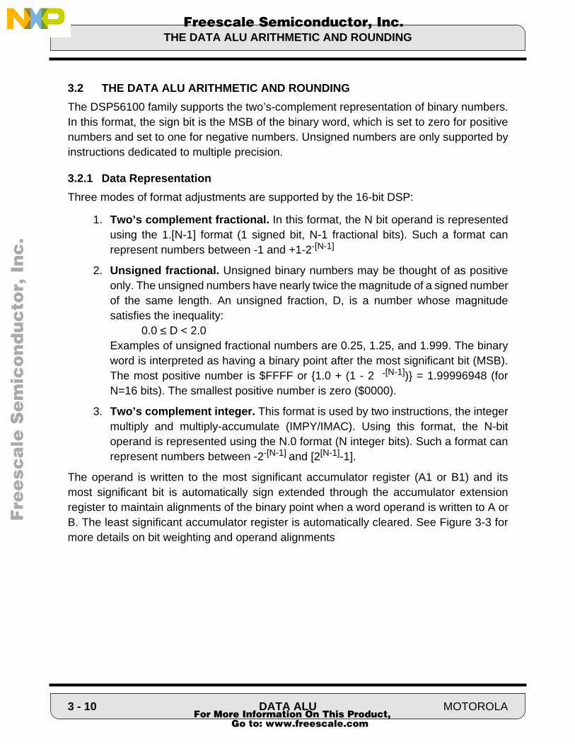
The DSP56100 family supports the two’s-complement representation of binary numbers.In this format, the sign bit is the MSB of the binary word, which is set to zero for positivenumbers and set to one for negative numbers. Unsigned numbers are only supported byinstructions dedicated to multiple precision.
3.2.1 Data Representation
Three modes of format adjustments are supported by the 16-bit DSP:
1. Two’s complement fractional. In this format, the N bit operand is representedusing the 1.[N-1] format (1 signed bit, N-1 fractional bits). Such a format canrepresent numbers between -1 and +1-2-[N-1]
2. Unsigned fractional. Unsigned binary numbers may be thought of as positiveonly. The unsigned numbers have nearly twice the magnitude of a signed numberof the same length. An unsigned fraction, D, is a number whose magnitudesatisfies the inequality: 0.0 ≤ D < 2.0 Examples of unsigned fractional numbers are 0.25, 1.25, and 1.999. The binaryword is interpreted as having a binary point after the most significant bit (MSB).The most positive number is $FFFF or 1.0 + (1 - 2 -[N-1]) = 1.99996948 (forN=16 bits). The smallest positive number is zero ($0000).
3. Two’s complement integer. This format is used by two instructions, the integermultiply and multiply-accumulate (IMPY/IMAC). Using this format, the N-bitoperand is represented using the N.0 format (N integer bits). Such a format canrepresent numbers between -2-[N-1]
and [2[N-1]-1].
The operand is written to the most significant accumulator register (A1 or B1) and itsmost significant bit is automatically sign extended through the accumulator extensionregister to maintain alignments of the binary point when a word operand is written to A orB. The least significant accumulator register is automatically cleared. See Figure 3-3 formore details on bit weighting and operand alignments
3 - 10 DATA ALU MOTOROLA For More Information On This Product,
Go to: www.freescale.com

THE DATA ALU ARITHMETIC AND ROUNDING
Fre
esc
ale
Se
mic
on
du
cto
r, I
Freescale Semiconductor, Inc.n
c..
.
.
3.2.2 Fractional Arithmetic
Figure 3-4 shows the Multiply-Accumulation implementation for fractional arithmetic. Themultiplication of two 16-bit signed fractional operands gives a 32-bit signed fractionalintermediate result with the LSB always set to zero. This intermediate result is added toone of the 40-bit accumulators. If rounding is specified in the MPY or MAC instruction(MACR or MPYR), the intermediate result will be rounded to 16 bits before being storedback to the destination accumulator
-20 2-15
-20 2-15 2-16 2-31
20 2-15 2-16 2-31-28
-215 20
-215 214 20
16-bit word operand X0,X1,Y0,Y1,A1,B1
32-bit long word operand
40-bit word operand A,B
Fractional 2’s Complement Representation
Integer 2’s Complement Representation
16-bit word operand X0,X1,Y0,Y1,A1,B1
16-bit word resultin A1,B1 unused
Figure 3-3 Bit Weighting and Alignments for Operands in
Fractional and Integer Representation
MOTOROLA DATA ALU 3 - 11 For More Information On This Product,
Go to: www.freescale.com

THE DATA ALU ARITHMETIC AND ROUNDING
Fre
esc
ale
Se
mic
on
du
cto
r, I
Freescale Semiconductor, Inc.n
c..
.
.
3.2.3 Integer Arithmetic
Figure 3-5 shows the Multiply and Multiply-Accumulate operations for integer arithmeticand Figure 3-6 describes the implementation of the Integer Multiply-Accumulate. Themultiplication/multiply-accumulate of two 16-bit signed integer operands (IMPY/IMAC)gives a 16-bit signed integer result in the MSP (A1 or B1). EXT (A2 or B2) is signextended and the LSP (A0 or B0) is unchanged. Since A0 and B0 remain unchanged byinteger arithmetic instructions, these two registers can be used as two additional dataALU registers when using IMAC, IMPY, INC24, DEC24, CLR24, SWAP, and EXTinstructions. Full precision 40-bit integer operations are possible using a fractional MPYor a series of MACs followed by an ASR instruction.
CAUTIONOverflow control and rounding are not performed during inte-ger multiplication and integer multiply-accumulate.
Integer arithmetic is optimized for new address generation using the multiplier. Forexample, when an address register Rn has to be updated to Rn + x0*y0 before fetchingnew data from memory, the following sequence of code can be used:
move Rn,a ;a=Rnimac x0,y0,a ;a1=Rn+x0*y0move x:(a1),b ;b1=X:<Rn+x0*y0>
Figure 3-4 Fractional Arithmetic
ss
0
16 bits 16 bits
31 bits
ss
40 bits
EXP MSP LSP
Signed FractionalInput Operands
Signed Intermediate
Multiplier Result
Signed FractionalMac Output
Input Operand 1 Input Operand 2
3 - 12 DATA ALU MOTOROLA For More Information On This Product,
Go to: www.freescale.com

THE DATA ALU ARITHMETIC AND ROUNDING
Fre
esc
ale
Se
mic
on
du
cto
r, I
Freescale Semiconductor, Inc.n
c..
.
Figure 3-5 Integer Arithmetic (IMPY/IMAC)
Signed Integer Output
31 bits
ss
16 bits 16 bits
unchanged EXP MSP
Signed IntegerInput Operands
SignedIntermediate
Multiplier Result
16 bits
0s
16 bits
S Ext.
Input Operand 1 Input Operand 2
Figure 3-6 IMAC Implementation
Multiply
16.0 16.0
31.1
=
39.1
=
39.1
>>15
Accumulator Shifter
Output Shifter<<15
Accumulate
16. 0S. ext.
MOTOROLA DATA ALU 3 - 13 For More Information On This Product,
Go to: www.freescale.com

THE DATA ALU ARITHMETIC AND ROUNDING
Fre
esc
ale
Se
mic
on
du
cto
r, I
Freescale Semiconductor, Inc.n
c..
.
3.2.4 Multiprecision Arithmetic Support
A set of data ALU operations is provided in order to facilitate multi-precision multiplica-tions. When these instructions are used, the multiplier accepts some combinations ofsigned twos-complement format and unsigned format. These instructions are:
1. MPY/MAC su: multiplication and multiply-accumulate with signed timesunsigned operands
2. MPY/MAC uu: multiplication and multiply-accumulate with unsigned timesunsigned operands
3. DMACss: multiplication with signed times signed operands and 16-bitarithmetic right shift of the accumulator before accumulation
4. DMACsu: multiplication with signed times unsigned operands and 16-bitarithmetic right shift of the accumulator before accumulation
5. DMACuu: multiplication with unsigned times unsigned operands and 16-bit arithmetic right shift of the accumulator before accumulation
Figure 3-7 shows how the DMAC instruction is implemented inside the Data ALU andFigure 3-8 illustrates the use of these instructions in the case of a double precision multi-plication. The signed x signed operation is used to multiply or multiply-accumulate thetwo upper, signed, portions of two signed double precision numbers. The unsigned xsigned operation is used to multiply or multiply-accumulate the upper, signed, portion ofone double precision number with the lower, unsigned, portion of the other double preci-sion number. The unsigned x unsigned operation is used to multiply or multiply-accumu-late the lower, unsigned, portion of one double precision number with the lower,unsigned, portion of the other double precision number.
3 - 14 DATA ALU MOTOROLA For More Information On This Product,
Go to: www.freescale.com

THE DATA ALU ARITHMETIC AND ROUNDING
Fre
esc
ale
Se
mic
on
du
cto
r, I
Freescale Semiconductor, Inc.n
c..
.
3.2.5 Rounding Modes
The DSP56100 family implements two types of rounding: convergent rounding and two’scomplement rounding. The type of rounding is selected by the OMR rounding bit (R bit).
3.2.5.1 Convergent Rounding
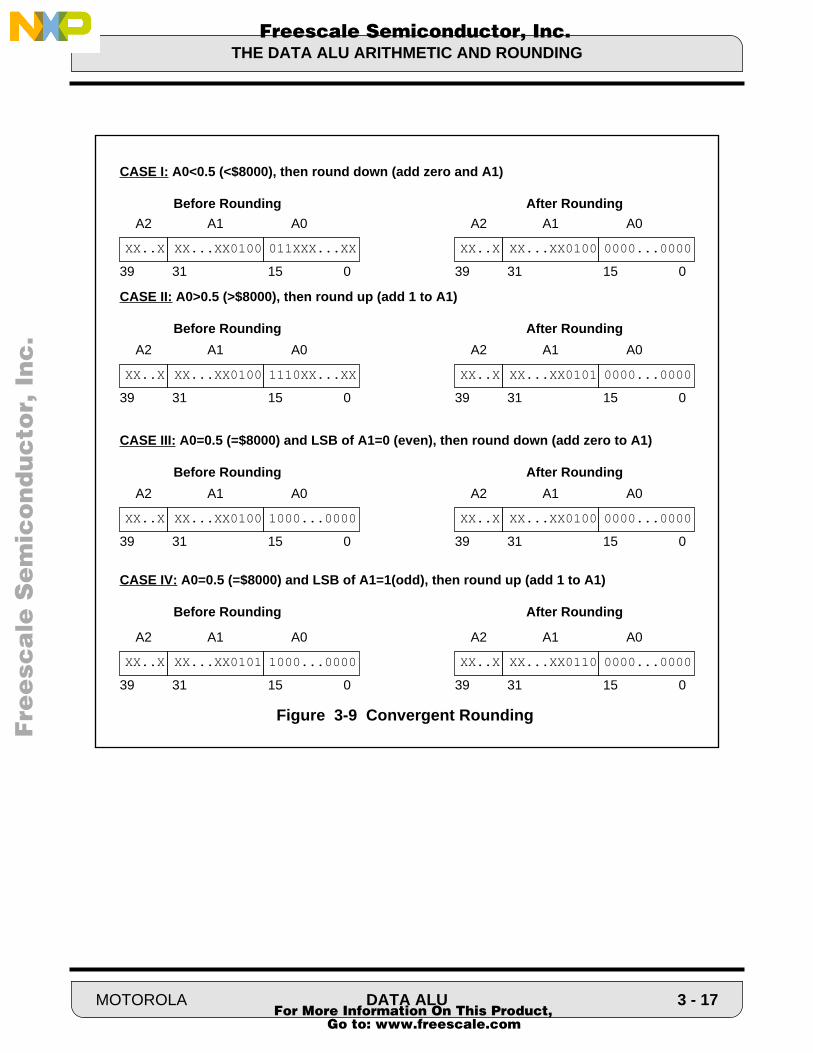
This is the default rounding mode. Convergent rounding is also called round-to-nearesteven number. It prevents the introduction of a bias normally produced by rounding downif the number is odd (LSB=1) and rounding up if the number is even (LSB=0). Figure 3-9shows the four possible cases for rounding a number in the A1 or B1 register. If the LeastSignificant Portion (LSP) of a number is less than half ($<8000) of the bit to be rounded(LSB), the number is rounded down and if the LSP of the number is greater than half ofthe LSB (>$8000) the number is rounded up. If the LSP is exactly equal to half of theLSB ($8000) and the LSB of the MSP is odd, the number is rounded up whereas if theLSB of the MSP is even, the number is rounded down i.e., truncated. This techniqueeliminates the bias in truncation rounding.
Block diagrams of the rounding implementations for the cases of no scaling, scalingdown and scaling up are shown in Figure 3-9, Figure 3-10, and Figure 3-11, respectively.Scaling modes require that the zero detect hardware and LSB Even gate have one ofthree forms since the LSB moves with the scaling mode.
Multiply
1.15 1.15
1.31
=
25.15 +=
9.31
9.31
>>16
Accumulator Shifter
Accumulate
Figure 3-7 DMAC Implementation
MOTOROLA DATA ALU 3 - 15 For More Information On This Product,
Go to: www.freescale.com

THE DATA ALU ARITHMETIC AND ROUNDING
Fre
esc
ale
Se
mic
on
du
cto
r, I
Freescale Semiconductor, Inc.n
c..
.
32 bits
64 bits
B0B1A0A1A2
X0X1
Y1 Y0
XLXH
YH YL
X
=
S Ext
++
+
XL x YL
XH x YL
YH x XL
XH x YH
Signed X Unsigned
Signed X Signed
Unsigned X Unsignedmpyuu x0,y0,amove a0,b0
dmacsu x1,y0,a
macsu y1,x0,amove a0,b1dmacss x1,y1,a
Figure 3-8 Double Precision Multiplication
3 - 16 DATA ALU MOTOROLA For More Information On This Product,
Go to: www.freescale.com
THE DATA ALU ARITHMETIC AND ROUNDING
Fre
esc
ale
Se
mic
on
du
cto
r, I
Freescale Semiconductor, Inc.n
c..
.
Figure 3-9 Convergent Rounding
XX..X XX...XX0100 011XXX...XX XX..X XX...XX0100 0000...0000
XX..X XX...XX0100 1110XX...XX XX..X XX...XX0101 0000...0000
XX..X XX...XX0101 1000...0000 XX..X XX...XX0110 0000...0000
XX..X XX...XX0100 1000...0000 XX..X XX...XX0100 0000...0000
A2 A1 A0
39 31 15 0
A2 A1 A0
39 31 15 0
A2 A1 A0
39 31 15 0
A2 A1 A0
39 31 15 0
A2 A1 A0
39 31 15 0
A2 A1 A0
39 31 15 0
A2 A1 A0
39 31 15 0
A2 A1 A0
39 31 15 0
CASE I: A0<0.5 (<$8000), then round down (add zero and A1)
Before Rounding After Rounding
CASE II: A0>0.5 (>$8000), then round up (add 1 to A1)
Before Rounding After Rounding
CASE III: A0=0.5 (=$8000) and LSB of A1=0 (even), then round down (add zero to A1)
Before Rounding After Rounding
CASE IV: A0=0.5 (=$8000) and LSB of A1=1(odd), then round up (add 1 to A1)
Before Rounding After Rounding
MOTOROLA DATA ALU 3 - 17 For More Information On This Product,
Go to: www.freescale.com

THE DATA ALU ARITHMETIC AND ROUNDING
F
ree
sca
le S
em
ico
nd
uc
tor,
I
Freescale Semiconductor, Inc.n
c..
.
.
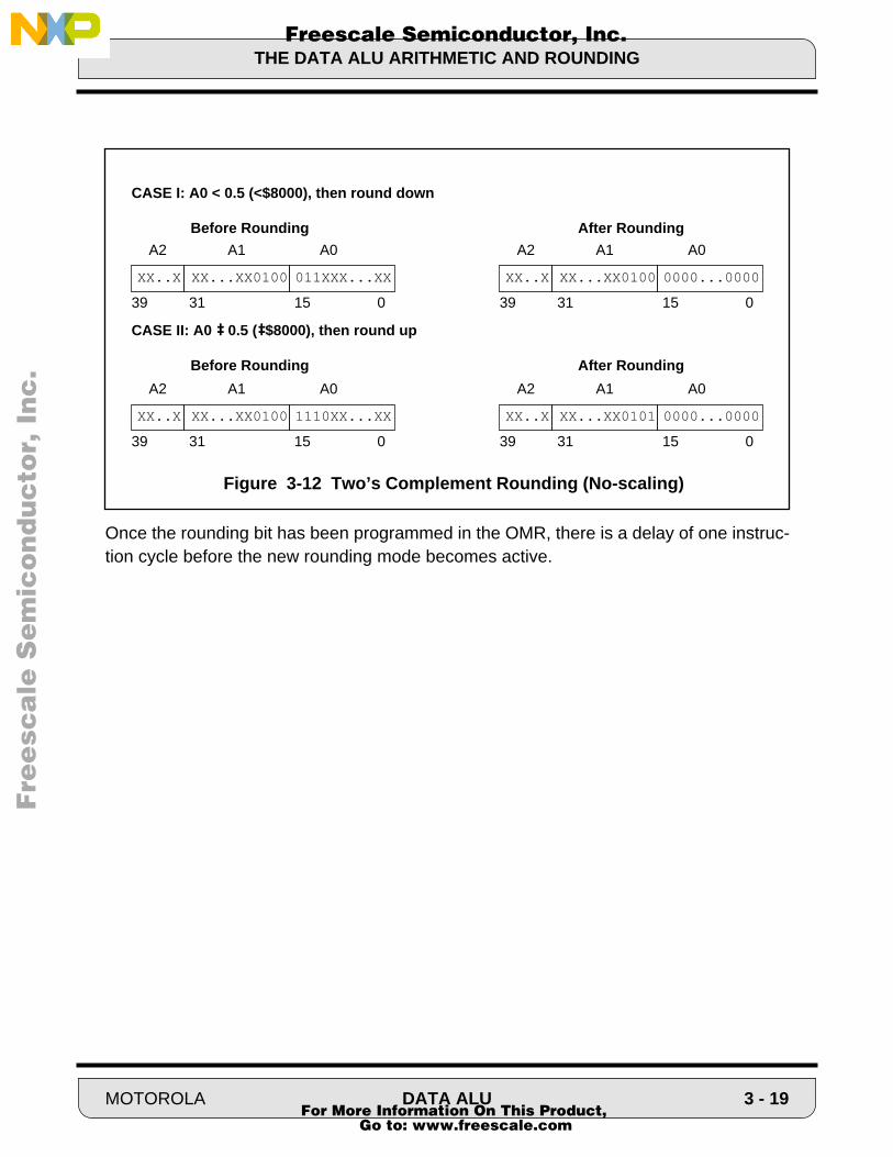
3.2.5.2 Two’s Complement Rounding
When twos-complement rounding is selected by setting the rounding bit in the OMR, oneis added to the bit to the right of the rounding point (bit 15 of A0 when no-scaling; bit 0 ofA1 when scaling down; bit 14 of A0 when scaling up) before the bit truncation during arounding operation. Figure 3-12 shows the two possible cases.
Accumulator
Add RoundingConstant
XXXXXXXXXXXXXXXXXXXXXXXXXXXXXXXXXXXXXXXX
1000000000000000000000000000000000000000
0
ZeroDetect
LSB even
Force LSP to zero
Figure 3-10 Convergent Rounding Implementation – No Scaling
Accumulator
Add RoundingConstant
XXXXXXXXXXXXXXXXXXXXXXXXXXXXXXXXXXXXXXXX
000000000000000000000000000000 100000000
0
ZeroDetect
LSB even
Force LSP to zero
Figure 3-11 Convergent Rounding Implementation – Scale Down
3 - 18 DATA ALU MOTOROLA For More Information On This Product,
Go to: www.freescale.com
THE DATA ALU ARITHMETIC AND ROUNDING
F
ree
sca
le S
em
ico
nd
uc
tor,
I
Freescale Semiconductor, Inc.n
c..
.
Once the rounding bit has been programmed in the OMR, there is a delay of one instruc-tion cycle before the new rounding mode becomes active.
XX..X XX...XX0100 011XXX...XX XX..X XX...XX0100 0000...0000
XX..X XX...XX0100 1110XX...XX XX..X XX...XX0101 0000...0000
A2 A1 A0
39 31 15 0
A2 A1 A0
39 31 15 0
A2 A1 A0
39 31 15 0
A2 A1 A0
39 31 15 0
CASE I: A0 < 0.5 (<$8000), then round down
Before Rounding After Rounding
CASE II: A0 ≥ 0.5 (≥$8000), then round up
Before Rounding After Rounding
Figure 3-12 Two’s Complement Rounding (No-scaling)
MOTOROLA DATA ALU 3 - 19 For More Information On This Product,
Go to: www.freescale.com

THE DATA ALU ARITHMETIC AND ROUNDING
F
ree
sca
le S
em
ico
nd
uc
tor,
I
Freescale Semiconductor, Inc.n
c..
.
3 - 20 DATA ALU MOTOROLA For More Information On This Product,
Go to: www.freescale.com

Fre
esc
ale
Se
mic
on
du
cto
r, I
Freescale Semiconductor, Inc.n
c..
.
SECTION 4
ADDRESS GENERATION UNIT (AGU)
MOTOROLA ADDRESS GENERATION UNIT (AGU) 4 - 1 For More Information On This Product,
Go to: www.freescale.com

SECTION CONTENTS
Fre
esc
ale
Se
mic
on
du
cto
r, I
Freescale Semiconductor, Inc.n
c..
.
4.1 INTRODUCTION . . . . . . . . . . . . . . . . . . . . . . . . . . . . . . . . . . . . . . . . 4-34.2 ADDRESS REGISTER FILE (Rn) . . . . . . . . . . . . . . . . . . . . . . . . . . . . 4-34.3 OFFSET REGISTER FILE (Nn) . . . . . . . . . . . . . . . . . . . . . . . . . . . . . 4-34.4 MODIFIER REGISTER FILE (Mn) . . . . . . . . . . . . . . . . . . . . . . . . . . . 4-44.5 TEMPORARY ADDRESS REGISTER . . . . . . . . . . . . . . . . . . . . . . . . 4-44.6 AGU STATUS REGISTER . . . . . . . . . . . . . . . . . . . . . . . . . . . . . . . . . 4-54.7 PC RELATIVE ADDRESSING UNIT . . . . . . . . . . . . . . . . . . . . . . . . . 4-64.8 SECONDARY OFFSET ADDER UNIT . . . . . . . . . . . . . . . . . . . . . . . . 4-64.9 MODULO ARITHMETIC UNIT . . . . . . . . . . . . . . . . . . . . . . . . . . . . . . 4-64.10 ADDRESSING MODES . . . . . . . . . . . . . . . . . . . . . . . . . . . . . . . . . . . 4-74.11 ADDRESS MODIFIER TYPES . . . . . . . . . . . . . . . . . . . . . . . . . . . . . . 4-12
4 - 2 ADDRESS GENERATION UNIT (AGU) MOTOROLA For More Information On This Product,
Go to: www.freescale.com

INTRODUCTION
Fre
esc
ale
Se
mic
on
du
cto
r, I
Freescale Semiconductor, Inc.n
c..
.
4.1 INTRODUCTIONThe major components of the AGU are:
• Address Register Files• Offset Register Files• Modifier Register Files• Address Arithmetic Unit Containing:
– Temporary Address Register– Local Status Register– PC Relative Addressing Unit– Secondary Offset Adder Unit– Modulo Arithmetic Unit– Address Output Multiplexer
A block diagram of the AGU is shown in Figure 4-1.
4.2 ADDRESS REGISTER FILE (Rn)The Address Register File consists of four, sixteen-bit registers. The file contains the ad-dress registers R0-R3 which usually contain addresses used as pointers to memory. Eachregister may be read or written by the Global Data Bus. High speed access to the XAB1and XAB2 buses is required to allow maximum access time for the internal and externalX Data Memory and Program Memory. Each address register may be used as an input tothe modulo arithmetic unit for a register update calculation. Each register may be writtenby the Global Data Bus or by the output of the modulo arithmetic unit.
R2, R3 and Temp may be used as inputs to a separate offset adder for an independentregister update calculation. This special update calculation occurs during parallel, dualreads (using R3) and during offset by absolute immediate offsets (using R2+$xx).
CAUTIONDue to pipelining, if an address register (M, N, or R) is changedwith a MOVE instruction, the new contents will not be available foruse as a pointer until the second following instruction.
4.3 OFFSET REGISTER FILE (Nn)The Offset Register File consists of four, sixteen-bit registers. The file contains the offsetregisters N0-N3 and usually contains offset values used to update address pointers. Eachoffset register may be read or written by the Global Data Bus. Each offset register is readwhen the same number address register is read and used as an input to the modulo arith-metic unit.
MOTOROLA ADDRESS GENERATION UNIT (AGU) 4 - 3 For More Information On This Product,
Go to: www.freescale.com

MODIFIER REGISTER FILE (Mn)
Fre
esc
ale
Se
mic
on
du
cto
r, I
Freescale Semiconductor, Inc.n
c..
.
4.4 MODIFIER REGISTER FILE (Mn)The Modifier Register File consists of four, 16-bit registers. The file contains the modifierregisters M0-M3 and usually specifies the type of arithmetic used to modify an addressregister during address register update calculations. Each modifier register may be reador written by the Global Data Bus. Each modifier register is read when the same numberaddress register is read and used as an input to the modulo arithmetic unit. Each modifierregister is preset to $FFFF during a processor reset.
4.5 TEMPORARY ADDRESS REGISTERThe temporary address register, Temp, is a 16-bit register which provides for:
r0
r1
r2
r3
temp
RB(0:15)
m0
m1
m2
m3
n0
n1
n2
n3
MB(0:15)
n3 only
NB(0:15)
UB(0:15)
XAB2(0:15) PAB(0:15)XAB1(0:15)
PDB(0:15)GDB(0:15)
ctrl ctrlctrlctrl Address Arithmetic
Unit
ModifierRegisterFile
OffsetRegisterFile Address Register
File
Figure 4-1 AGU Block Diagram
4 - 4 ADDRESS GENERATION UNIT (AGU) MOTOROLA For More Information On This Product,
Go to: www.freescale.com

AGU STATUS REGISTER
Fre
esc
ale
Se
mic
on
du
cto
r, I
Freescale Semiconductor, Inc.n
c..
.
1. temporary storage for an absolute address loaded from the Program Data Bus,
2. the immediate data loaded from the Global Data Bus,
3. Address Register Indirect with Immediate Displacement addressing mode,
4. the contents of A1 or B1 registers used by the Accumulator Register IndirectAddressing mode, or
5. the output of the modulo arithmetic unit.
The modulo arithmetic unit output is loaded into the Temp register during the pre-updatecycle of the indexed by offset addressing mode, of the pre-decrement addressing mode,and during the LEA instruction. In each of these addressing modes, an address registeris accessed, updated by the modulo arithmetic unit, and stored in Temp in one instructioncycle. In the following cycle, the content of Temp is used to address the X memory. Forall absolute addressing modes, the address of the operand is written into Temp and thenused to address X: or P: memory.
4.6 AGU STATUS REGISTERThe 3-bit local status register in the AGU, which cannot be accessed by the user, will beupdated after every register update; i.e., only those addressing modes that update the ad-dress register regardless of memory access type.
Updating of the local status register is as follows:
sr_v ← set if the modulo circuit performed a wrap, clear otherwise.
sr_z ← set if the result of the address update is zero, clear otherwise.
sr_n ← set if the result of the address update is negative, clear otherwise.
The CHKAAU instruction will copy the AGU status register to SR as follows:
V ← sr_v
Z ← sr_z
N ← sr_n
During double parallel reads, only the update of the address register used for the first par-allel read (not r3) will affect the local status register.
Note: Only the V, Z, N bits of SR will be changed.
MOTOROLA ADDRESS GENERATION UNIT (AGU) 4 - 5 For More Information On This Product,
Go to: www.freescale.com
PC RELATIVE ADDRESSING UNIT
Fre
esc
ale
Se
mic
on
du
cto
r, I
Freescale Semiconductor, Inc.n
c..
.
4.7 PC RELATIVE ADDRESSING UNITThe PC Relative Addressing Unit performs the PC relative address computation with signextension done on the program address offset. The result is gated onto the Program Ad-dress Bus by a control signal from the program controller.
4.8 SECONDARY OFFSET ADDER UNITThe Secondary Offset Adder Unit is used for an address update calculation during doubledata memory read instructions, or for the addition of address register and immediate dis-placement.
4.9 MODULO ARITHMETIC UNITThe Modulo Arithmetic Unit contains one 16-bit full adder (called the offset adder) whichmay add one, subtract one, or add the contents of the respective signed offset register Nto the contents of the selected address register. A second full adder (called the moduloadder) adds the summed result of the first full adder to a modulo value M or minus M,where M is stored in the respective modifier register. A third full adder (called the reversecarry adder) adds the constant one, minus one, the offset N (stored in the respective offsetregister) to the selected address register with the carry propagating in the reverse direc-tion, from the most significant bit to the least. The offset adder and the reverse carry adderare in parallel and share common inputs. Test logic determines which of the threesummed outputs of the full adders is output to the address register file or temporary reg-ister.
The modulo arithmetic unit can update one address register, Rn, during one instructioncycle. It is capable of performing linear, reverse carry, and modulo arithmetic. The con-tents of the selected modifier register specifies the type of arithmetic required in an ad-dress register update calculation. The modifier value is decoded in the modulo arithmeticunit and affects the unit’s operation. The modulo arithmetic unit’s operation is data-depen-dent and requires execution cycle decoding of the selected modifier register contents.Note that for dual reads, there is no modulo capability for an R3 update, linear arithmeticwill be used.
The output of the offset adder gives the result of linear arithmetic (e.g. Rn+1; Rn+N) andis selected as the modulo arithmetic unit’s output for linear arithmetic addressing modifi-ers. The reverse carry adder performs the required operation for reverse carry arithmeticand its output is selected as the modulo arithmetic unit’s output for reverse carry address-ing modifiers. Reverse carry arithmetic is useful for 2k point FFT addressing. For moduloarithmetic, the modulo arithmetic unit will perform the function (Rn+N) modulo M where Ncan be one, minus one, or the contents of the offset register Nn. If the modulo operation
4 - 6 ADDRESS GENERATION UNIT (AGU) MOTOROLA For More Information On This Product,
Go to: www.freescale.com
ADDRESSING MODES
Fre
esc
ale
Se
mic
on
du
cto
r, I
Freescale Semiconductor, Inc.n
c..
.
requires wraparound for modulo arithmetic, the summed output of the modulo adder willgive the correct updated address register value; otherwise, if wraparound is not neces-sary, the output of the offset adder gives the correct result.
The test logic will determine which output address to select. If the contents of the respec-tive modifier register, M, specify linear or reverse carry arithmetic, the output of the mod-ulo arithmetic unit will be the output of the offset adder or reverse carry adder,respectively. If M specifies a modulo value (modulo arithmetic) the output of the moduloarithmetic unit will be based on the results or both the offset and modulo adders.
The modulo arithmetic unit is also used in a special way during execution of the NORMinstruction. For the NORM instruction, the modulo arithmetic unit computes three values:Rn, Rn-1 and Rn+1. Depending on the result of the Data ALU operation, one of the threeis selected for the register update. (See the NORM instruction in Appendix A)
4.10 ADDRESSING MODES The DSP56100 family instruction set contains a full set of operand addressing modes. Alladdress calculations are performed in the Address Generation Unit to minimize executiontime and loop overhead.
Addressing modes specify whether the operand(s) is in a register or memory and providethe specific address of the operand(s). An effective address in an instruction will specifyan addressing mode, and for some addressing modes, the effective address will furtherspecify an address register. In addition, address register indirect modes require additionaladdress modifier information which is not encoded in the instruction. The address modifierinformation is specified in the selected address modifier register(s). All memory referenc-es require one address modifier and the dual X memory reference requires one or two ad-dress modifiers. The definition of certain instructions implies the use of specific registersand the addressing modes used.
Address register indirect modes require an offset and a modifier register for use in ad-dress calculations. These registers are implied by the address register specified in an ef-fective address in the instruction word. Each offset register Nn and each modifier register,Mn, is assigned to an address register, Rn, having the same register number, n, forminga triplet. Thus the assigned triplets are M0;N0;R0, M1;N1;R1, M2;N2;R2, and M3;N3;R3.The address register Rn is used as the address register, the offset register, Nn, is usedto specify an optional offset and the modifier register Mn is used to specify an addressingmode modifier.
MOTOROLA ADDRESS GENERATION UNIT (AGU) 4 - 7 For More Information On This Product,
Go to: www.freescale.com

ADDRESSING MODES
Fre
esc
ale
Se
mic
on
du
cto
r, I
Freescale Semiconductor, Inc.n
c..
.
The addressing modes are grouped into three categories: register direct, address registerindirect, and special. These addressing modes are described below and summarized inTable 4-1.
4.10.1 Register Direct Modes These effective addressing modes specify that the operand is in one (or more) of the 10Data ALU registers, 12 address registers or 7 control registers.
4.10.1.1 Data or Control Register Direct The operand is in one, two, or three Data ALU register(s) as specified in a portion of thedata bus movement field in the instruction. This addressing mode is also used to specifya control register operand for special instructions. This reference is classified as a registerreference.
4.10.1.2 Address Register Direct The operand is in one of the 12 address registers (Rn, Mn, and Nn) specified by an effec-tive address in the instruction. This reference is classified as a register reference.
CAUTIONDue to pipelining, if an address register (Mn, Nn, or Rn) is changed with aMOVE instruction, the new contents will not be available for use as a pointeruntil the second following instruction.
4.10.2 Address Register Indirect Modes The effective address in the instruction specifies the address register Rn and the addresscalculation to be performed. These addressing modes specify that the operand(s) is inmemory and provide the specific address of the operand(s). When an address register isused to point to a memory location, the addressing mode is called address register indi-rect. The term indirect is used because the operand is not the address register itself, butthe contents of the memory location pointed to by the address register. A portion of thedata bus movement field in the instruction specifies the memory reference to be per-formed. The type of address arithmetic used is specified by the address modifier register,Mn.
4.10.2.1 No Update (Rn)The address of the operand is in the address register Rn. The contents of the Rn registerare unchanged. The Mn and Nn registers are ignored. This reference is classified as amemory reference.
4 - 8 ADDRESS GENERATION UNIT (AGU) MOTOROLA For More Information On This Product,
Go to: www.freescale.com
ADDRESSING MODES
Fre
esc
ale
Se
mic
on
du
cto
r, I
Freescale Semiconductor, Inc.n
c..
.
4.10.2.2 Postincrement by 1 (Rn)+The address of the operand is in the address register Rn. After the operand address isused, it is incremented by 1 and stored in the same address register. The type of arith-metic used to increment Rn is determined by Mn. The Nn register is ignored. This refer-ence is classified as a memory reference.
4.10.2.3 Postdecrement by 1 (Rn)-The address of the operand is in the address register Rn. After the operand address isused, it is decremented by 1 and stored in the same address register. The type of arith-metic used to increment Rn is determined by Mn. The Nn register is ignored. This refer-ence is classified as a memory reference.
4.10.2.4 Postincrement by Offset Nn (Rn)+NnThe address of the operand is in the address register Rn. After the unsigned operand ad-dress is used, the contents of the Nn register are added to Rn and stored in the same ad-dress register. The content of Nn is treated as a 2’s complement number and can there-fore be interpreted as signed or unsigned. The contents of the Nn register are unchanged.The type of arithmetic used to increment Rn is determined by Mn. This reference is clas-sified as a memory reference.
4.10.2.5 Indexed by Offset Nn (Rn+Nn)The address of the operand is the sum of the contents of the address register Rn and thecontents of the address offset register Nn. This addition occurs before the operand canbe accessed and therefore requires an extra instruction cycle. The content of Nn is treatedas a 2’s complement number and can therefore be interpreted as signed or unsigned. Thecontents of the Rn and Nn registers are unchanged. The type of arithmetic used to addNn to Rn is determined by Mn. This reference is classified as a memory reference.
4.10.2.6 Predecrement by 1 -(Rn)The address of the operand is the contents of the address register Rn decremented by 1.Before the operand address is used, it is decremented (subtracted) by 1 and stored in thesame address register. The type of arithmetic used to increment Rn is determined by Mn.The Nn register is ignored. This reference is classified as a memory reference.
4.10.3 PC Relative Modes In the PC relative addressing modes used in the BRA and DO instructions, the addressof the operand is obtained by adding a displacement, represented in two’s complementformat, to the value of the program counter (PC). The PC always points to the address of
MOTOROLA ADDRESS GENERATION UNIT (AGU) 4 - 9 For More Information On This Product,
Go to: www.freescale.com

ADDRESSING MODES
Fre
esc
ale
Se
mic
on
du
cto
r, I
Freescale Semiconductor, Inc.n
c..
.
the next instruction, so PC relative addressing with zero displacement will produce the ad-dress of the next sequential instruction in program memory.
4.10.3.1 Long Displacement PC Relative This addressing mode requires one word of instruction extension. The address of the op-erand is the sum of the contents of the PC and the extension word. This reference is clas-sified as a register reference.
4.10.3.2 Short Displacement PC Relative The short displacement occupies 8 bits in the instruction operation word. The displace-ment is first sign extended to 16 bits and then added to the PC to obtain the address ofthe operand. This reference is classified as both a register reference and a memory ref-erence.
4.10.3.3 Address Register PC Relative The address of the operand is the sum of the contents of the address register Rn and thePC. The Mn and Nn registers are ignored. This reference is classified as a register refer-ence.
4.10.4 Special Address Modes The special address modes do not use an address register in specifying an effective ad-dress. These modes specify the operand or the address of the operand in a field of theinstruction or they implicitly reference an operand.
4.10.4.1 Upper Word of AccumulatorThis addressing mode uses the contents of either A1 or B1 to address an operand inmemory. No update is performed. It is available for single parallel memory moves. Thisreference is classified as an X memory reference.
4.10.4.2 Immediate Data This addressing mode requires one word of instruction extension. The immediate data isa word operand in the extension word of the instruction. This reference is classified as aprogram reference.
4 - 10 ADDRESS GENERATION UNIT (AGU) MOTOROLA For More Information On This Product,
Go to: www.freescale.com

ADDRESSING MODES
Fre
esc
ale
Se
mic
on
du
cto
r, I
Freescale Semiconductor, Inc.n
c..
.
4.10.4.3 Immediate Short Data The 8-bit operand is in the instruction operation word. The 8-bit operand is used for theANDI, DO, ORI, and REP instructions in addition to the immediate move to register in-struction. This reference is classified as a program reference.
4.10.4.4 Absolute Address This addressing mode requires one word of instruction extension. The address of the op-erand is in the extension word. This reference is classified as both a memory referenceand a program reference.
4.10.4.5 Absolute Short Address For the Absolute Short addressing mode the address of the operand occupies 5 bits in theinstruction operation word and is zero extended. This reference is classified as both amemory reference and a program reference.
4.10.4.6 Short Jump Address The operand occupies 8 bits in the instruction operation word. The address is zero extend-ed to 16 bits and is unsigned. This reference is classified as a program memory reference.
4.10.4.7 I/O Short Address For the I/O short addressing mode the address of the operand occupies 5 bits in the in-struction operation word and is one’s extended. I/O short is used with the bit manipulationand move peripheral data instructions. This reference is classified as an X memory refer-ence.
4.10.4.8 Implicit Reference Some instructions make implicit reference to the program counter (PC), system stack(SSH, SSL), loop address register (LA), loop counter (LC), or status register (SR). Theregisters implied and their use are defined by the individual instruction descriptions (seeAppendix A). This reference is classified as both a register reference and a program ref-erence.
4.10.4.9 Indexed by Short DisplacementThis addressing mode uses one extension word which contains the 8-bit short index andprecedes the opcode word. The index requires an extra instruction cycle and always in-dexes address register R2. This addressing mode is available for MOVEM and MOVEC
MOTOROLA ADDRESS GENERATION UNIT (AGU) 4 - 11 For More Information On This Product,
Go to: www.freescale.com

ADDRESS MODIFIER TYPES
Fre
esc
ale
Se
mic
on
du
cto
r, I
Freescale Semiconductor, Inc.n
c..
.
instructions as well as single parallel memory moves. This reference is classified as an Xmemory reference.
4.10.5 Addressing Modes Summary Table 4-2 contains a summary of the addressing modes discussed in the previous para-graphs.
4.11 ADDRESS MODIFIER TYPES The DSP56100 family Address Generation Unit supports linear, modulo, and bit-reversedaddress arithmetic for all address register indirect modes. Address modifiers determinethe type of arithmetic used to update addresses. Address modifiers allow the creation ofdata structures in memory for FIFOs (queues), delay lines, circular buffers, stacks, andbit-reversed FFT buffers. Data is manipulated by updating address registers (pointers)rather than moving large blocks of data. The contents of the address modifier register, Mn,defines the type of address arithmetic to be performed for addressing mode calculations,and for the case of modulo arithmetic, the contents of Mn also specifies the modulus. Alladdress register indirect modes may be used with any address modifier type. Each ad-dress register Rn has its own modifier register Mn associated with it.
4.11.1 Linear Modifier The address modification is performed using normal 16-bit (modulo 65,536) two’s com-plement linear arithmetic. A 16-bit offset Nn, or immediate data (+1, -1, or a displacementvalue) may be used in the address calculations. The range of values may be consideredas signed (Nn from -32,768 to +32,767) or unsigned (Nn from 0 to +65,536). There is noarithmetic differences between these two data representations. Addresses are normallyconsidered unsigned, data is normally considered signed.
4.11.2 Reverse Carry Modifier The address modification is performed by propagating the carry in the reverse direction,i.e., from the MSB to the LSB. This is equivalent to bit-reversing the contents of Rn andthe offset value Nn, adding normally, and then bit-reversing the result. If the (Rn)+Nn ad-dressing mode is used with this address modifier, and Nn contains the value 2k-1 (a powerof two), then postincrementing by Nn is equivalent to bit-reversing the k LSBs of Rn, in-crementing Rn by 1, and bit-reversing the k LSBs of Rn again. This address modificationis useful for 2k point FFT addressing. The range of values for Nn is 0 to +32,767. This al-lows bit-reversed addressing for FFTs up to 65,536 points.
4 - 12 ADDRESS GENERATION UNIT (AGU) MOTOROLA For More Information On This Product,
Go to: www.freescale.com

ADDRESS MODIFIER TYPES
Fre
esc
ale
Se
mic
on
du
cto
r, I
Freescale Semiconductor, Inc.n
c..
.
As an example, consider a 1024 point FFT with real data stored in one section of dataRAM and imaginary data stored in another section of data RAM. Then Nn would containthe value 512 and postincrementing by +N would generate the address sequence 0, 512,256, 768, 128, 640, … This is the scrambled FFT data order for sequential frequencypoints from 0 to 2π. For proper operation the reverse carry modifier restricts the base ad-dress of the bit reversed data buffer to an integer multiple of 2k, such as 1024, 2048, 3072,etc. The use of addressing modes other than postincrement by Nn is possible but may notprovide a useful result.
4.11.3 Modulo Modifier The address modification is performed modulo M, where M is permitted to range from 2to +32,768. Modulo M arithmetic causes the address register value to remain within anaddress range of size M defined by a lower and upper address boundary. The value M-1is stored in the modifier register Mn, thus allowing a modulo size range from 2 to 32,768.The lower boundary (base address) value must have zeroes in the k LSBs, where 2k > M,and therefore must be a multiple of 2k. The upper boundary is the lower boundary plus themodulo size minus one (base address plus M-1).
For example, to create a circular buffer of 24 stages, M is chosen as 24 and the lower ad-dress boundary must have its 5 LSBs equal to zero (2k > 24, thus k > 5). The Mn registeris loaded with the value 23 (M-1). The lower boundary may be chosen as 0, 32, 64, 96,128, 160, etc. The upper boundary of the buffer is then the lower boundary plus 23.
The address pointer is not required to start at the lower address boundary and may beginanywhere within the defined modulo address range. In fact, the initial location of Rn de-termines the lower and upper boundaries. The upper and lower boundaries are not explic-itly needed. If the address register pointer increments past the upper boundary of the buff-er (base address plus M-1) it will wrap around to the base address. If the address decre-ments past the lower boundary (base address) it will wrap around to the base addressplus M-1.
If an offset Nn is used in the address calculations, the 16-bit value Nn must be less thanor equal to M for proper modulo addressing. This is because a single modulo wrap aroundis detected. If Nn is greater than M, the result is data dependent and unpredictable exceptfor the special case where Nn=L*(2k), a multiple of the block size, 2k, where L is a positiveinteger. Note that the offset Nn must be a positive two’s complement integer. For this casethe pointer Rn will be incremented using linear arithmetic to the same relative address Lblocks forward in memory. For the normal case where Nn is less than or equal to M, themodulo arithmetic unit will automatically wrap the address pointer around by the requiredamount. This type of address modification is useful in creating circular buffers for FIFOs
MOTOROLA ADDRESS GENERATION UNIT (AGU) 4 - 13 For More Information On This Product,
Go to: www.freescale.com
ADDRESS MODIFIER TYPES
Fre
esc
ale
Se
mic
on
du
cto
r, I
Freescale Semiconductor, Inc.n
c..
.
Operand ReferenceUses Mn
Addressing Mode Modifier S C D A P X XX
Register Direct
Data or Control Register No X X XAddress Register Rn No XAddress Modifier Register MnNo XAddress Offset Register Nn No X
Address Register Indirect
No Update No X XPostincrement by 1 Yes* X X XPostdecrement by 1 Yes X XPostincrement by Offset Nn Yes* X X XIndexed by Offset Nn Yes XPredecrement by 1 Yes X
PC Relative
Long Displacement No XShort Displacement No X XAddress Register No X X
Special
Upper word of accumulator No XImmediate Data No XImmediate Short Data No XAbsolute Address No X XAbsolute Short Address No X XShort Jump Address No XI/O Short Address No XImplicit No X X XIndexed by short displacement No X
Where:S = System Stack ReferenceP = Program Memory ReferenceC =Program Controller Register ReferenceX = X Memory ReferenceD = Data ALU Register ReferenceXX = Double X Memory ReadA = Address ALU Register Reference
*note: M3 is not used for updating R3 in the second read in the X memory
Table 4-1 DSP56100 Family Addressing Modes
4 - 14 ADDRESS GENERATION UNIT (AGU) MOTOROLA For More Information On This Product,
Go to: www.freescale.com

ADDRESS MODIFIER TYPES
Fre
esc
ale
Se
mic
on
du
cto
r, I
Freescale Semiconductor, Inc.n
c..
.
(queues), delay lines, and sample buffers up to 32,768 words long. It is also used for dec-imation, interpolation, and waveform generation. The special case of (Rn)+Nn withNn=L*(2k) is useful for performing the same algorithm on multiple buffers, for example im-plementing a bank of parallel filters. The range of values for Nn is -32,768 to +32,767 al-though all values are not useful when modulo addressing as described above.
4.11.4 Wrap-Around Modulo Modifier The address modification is performed modulo M, where M may be any power of 2 in therange from 21 to 215. Modulo M arithmetic causes the address register value to remainwithin an address range of size M defined by a lower and upper address boundary. Thelower boundary (base address) value must have zeroes in the k LSBs, where 2k = M, andtherefore must be a multiple of 2k. The upper boundary is the lower boundary plus themodulo size minus one (base address plus M-1).
For example, to create a circular buffer of 32 stages, M is chosen as 32 and the lower ad-dress boundary must have its 5 LSBs equal to zero (2k = 32, thus k = 5). The Mn registeris loaded with the value $001F. The lower boundary may be chosen as 0, 32, 64, 96, 128,160, etc. The upper boundary of the buffer is then the lower boundary plus 31.
The address pointer is not required to start at the lower address boundary and may beginanywhere within the defined modulo address range (between the lower and upper bound-aries). If the address register pointer increments past the upper boundary of the buffer(base address plus M-1) it will wrap around to the base address. If the address decre-ments past the lower boundary (base address) it will wrap around to the base addressplus M-1. If an offset Nn is used in the address calculations, the 16-bit value Nn is requiredto be less than or equal to M for proper modulo addressing since multiple wrap around isnot supported. The range of values for Nn is -32,768 to +32,767.
This type of address modification is useful for decimation, interpolation, and waveformgeneration since the multiple wrap-around capability may be used for argument reduction.
MOTOROLA ADDRESS GENERATION UNIT (AGU) 4 - 15 For More Information On This Product,
Go to: www.freescale.com
ADDRESS MODIFIER TYPES
F
ree
sca
le S
em
ico
nd
uc
tor,
I
Freescale Semiconductor, Inc.n
c..
.
4.11.5 Address Modifier Type Encoding Summary Table 4-2 contains a summary of the address modifier types discussed in the previousparagraphs.
16-bit Modifier Reg. (M0-M3)MMMMMMMMMMMMMMMM Address Calculation Arithmetic
0000000000000000 Reverse Carry (Bit Reversed)0000000000000001 Modulo 20000000000000010 Modulo 3
.
.0111111111111110 Modulo 327670111111111111111 Modulo 32768
1000000000000000 Reserved.
1111111111111110 Reserved1111111111111111 Linear (Modulo 65536)
where MMMMMMMMMMMMMMMM = 16-bit Modifier Reg. Contents
Table 4-2 Addressing Mode Modifier Summary
4 - 16 ADDRESS GENERATION UNIT (AGU) MOTOROLA For More Information On This Product,
Go to: www.freescale.com

Fre
esc
ale
Se
mic
on
du
cto
r, I
Freescale Semiconductor, Inc.n
c..
.
SECTION 5
PROGRAM CONTROL UNIT (PCU)
MOTOROLA PROGRAM CONTROL UNIT (PCU) 5 - 1 For More Information On This Product,
Go to: www.freescale.com

SECTION CONTENTS
Fre
esc
ale
Se
mic
on
du
cto
r, I
Freescale Semiconductor, Inc.n
c..
.
5.1 INTRODUCTION . . . . . . . . . . . . . . . . . . . . . . . . . . . . . . . . . . . . . . . . 5-35.2 PROGRAM COUNTER (PC) . . . . . . . . . . . . . . . . . . . . . . . . . . . . . . . 5-35.3 STATUS REGISTER (SR) . . . . . . . . . . . . . . . . . . . . . . . . . . . . . . . . . 5-45.3.1 Carry (Bit 0) . . . . . . . . . . . . . . . . . . . . . . . . . . . . . . . . . . . . . . . . . . . . . 5-45.3.2 Overflow (Bit 1) . . . . . . . . . . . . . . . . . . . . . . . . . . . . . . . . . . . . . . . . . . 5-45.3.3 Zero (Bit 2) . . . . . . . . . . . . . . . . . . . . . . . . . . . . . . . . . . . . . . . . . . . . . 5-45.3.4 Negative (Bit 3) . . . . . . . . . . . . . . . . . . . . . . . . . . . . . . . . . . . . . . . . . . 5-45.3.5 Unnormalized (Bit 4) . . . . . . . . . . . . . . . . . . . . . . . . . . . . . . . . . . . . . . 5-55.3.6 Extension (Bit 5) . . . . . . . . . . . . . . . . . . . . . . . . . . . . . . . . . . . . . . . . . 5-65.3.7 Limit (Bit 6) . . . . . . . . . . . . . . . . . . . . . . . . . . . . . . . . . . . . . . . . . . . . . 5-65.3.8 Sticky Bit (Bit 7) . . . . . . . . . . . . . . . . . . . . . . . . . . . . . . . . . . . . . . . . . . 5-65.3.9 Interrupt Masks (Bits 8,9) . . . . . . . . . . . . . . . . . . . . . . . . . . . . . . . . . . 5-75.3.10 Scaling Mode (Bits 10,11) . . . . . . . . . . . . . . . . . . . . . . . . . . . . . . . . . . 5-75.3.11 Reserved Status (Bits 12,13) . . . . . . . . . . . . . . . . . . . . . . . . . . . . . . . 5-85.3.12 ForeVer Flag (Bit 14) . . . . . . . . . . . . . . . . . . . . . . . . . . . . . . . . . . . . . 5-85.3.13 Loop Flag (Bit 15) . . . . . . . . . . . . . . . . . . . . . . . . . . . . . . . . . . . . . . . . 5-85.4 LOOP COUNTER (LC) . . . . . . . . . . . . . . . . . . . . . . . . . . . . . . . . . . . . 5-85.5 LOOP ADDRESS REGISTER (LA) . . . . . . . . . . . . . . . . . . . . . . . . . . 5-85.6 SYSTEM STACK (SS) . . . . . . . . . . . . . . . . . . . . . . . . . . . . . . . . . . . . 5-95.7 STACK POINTER (SP) . . . . . . . . . . . . . . . . . . . . . . . . . . . . . . . . . . . . 5-95.7.1 Stack Pointer (Bits 0,1,2,3) . . . . . . . . . . . . . . . . . . . . . . . . . . . . . . . . . 5-105.7.2 Stack Error Flag - SE (Bit 4) . . . . . . . . . . . . . . . . . . . . . . . . . . . . . . . . 5-105.7.3 Underflow Flag - UF (Bit 5) . . . . . . . . . . . . . . . . . . . . . . . . . . . . . . . . . 5-115.7.4 Unimplemented Stack Pointer Register bits . . . . . . . . . . . . . . . . . . . . 5-125.8 OPERATING MODE REGISTER (OMR) . . . . . . . . . . . . . . . . . . . . . . 5-125.8.1 Operating Mode Bits (Bits 0,1) . . . . . . . . . . . . . . . . . . . . . . . . . . . . . . 5-135.8.2 Bus Arbitration Mode Bit (Bit 2) . . . . . . . . . . . . . . . . . . . . . . . . . . . . . . 5-145.8.3 Saturation Bit (Bit 4) . . . . . . . . . . . . . . . . . . . . . . . . . . . . . . . . . . . . . . 5-145.8.4 Rounding Bit (Bit 5) . . . . . . . . . . . . . . . . . . . . . . . . . . . . . . . . . . . . . . . 5-155.8.5 Stop Delay Bit (Bit 6) . . . . . . . . . . . . . . . . . . . . . . . . . . . . . . . . . . . . . . 5-155.8.6 Clock Out Disable Bit (Bit 7) . . . . . . . . . . . . . . . . . . . . . . . . . . . . . . . . 5-155.8.7 Reserved Operating Mode Register Bits (Bits 3 and 8-15) . . . . . . . . . 5-15
5 - 2 PROGRAM CONTROL UNIT (PCU) MOTOROLA For More Information On This Product,
Go to: www.freescale.com
INTRODUCTION
Fre
esc
ale
Se
mic
on
du
cto
r, I
Freescale Semiconductor, Inc.n
c..
.
5.1 INTRODUCTIONThe PCU performs program address generation (instruction prefetch), instruction decod-ing, hardware DO-loop control, and exception processing. The programmer views thePCU as consisting of six registers and a hardware system stack (SS) as shown on Fig-ure 5-1. In addition to the standard program flow-control resources, such as a programcounter (PC), complete status register (SR), and SS, the PCU features registers (loopaddress LA and loop counter LC) dedicated to supporting the hardware DO loop instruc-tion.
5.2 PROGRAM COUNTER (PC)This 16-bit register contains the address of the next location to be fetched from ProgramMemory Space. The PC may point to instructions, data operands or addresses of oper-ands. References to this register are always inherent and are implied by most instruc-tions. This special purpose address register is stacked when program looping is initiated,when a branch or a jump to subroutine is performed, and when interrupts occur exceptfor fast interrupts (refer to Section 7.3.4.1).
Figure 5-1 Program Control Unit Block Diagram
16 bit 16 bit
16 bit 16 bit
123456789
101112131415
SSH SSLSP
MRPC
LCLA
CCR
16 bit
16 bit 16 bit
6 bit
OMR
MOTOROLA PROGRAM CONTROL UNIT (PCU) 5 - 3 For More Information On This Product,
Go to: www.freescale.com

STATUS REGISTER (SR)
Fre
esc
ale
Se
mic
on
du
cto
r, I
Freescale Semiconductor, Inc.n
c..
.
5.3 STATUS REGISTER (SR)The status register is a 16-bit register consisting of an 8-bit Mode register (MR) and an 8-bit Condition Code register (CCR). The MR register is the high-order 8 bits of the statusregister; the CCR register is the low-order 8 bits.
The MR bits are only affected by processor reset, exception processing, the DO,ENDDO, RTI, and SWI instructions and by instructions which directly reference the MRregister (e.g., ANDI, ORI). During processor reset, the interrupt mask bits of themode register will be set, the scaling mode bits, loop flag, sticky bit, and the for-ever flag will be cleared. The CCR is a special purpose control register which definesthe current user state of the processor at any given time. The CCR bits are affected bydata ALU operations, one address ALU operation (CHKAAU), bit field manipulationinstructions, parallel move operations, and by instructions which directly reference theCCR register. The CCR bits are not affected by data transfers over XDB except if datalimiting occurs when reading the A or B accumulators. During processor reset, all CCRbits are cleared. The standard definition of the CCR bits is given below. Refer to Appen-dix A, Section A.3 for the complete CCR bit computation rules. The SR register isstacked when program looping is initialized when a jump or branch to subroutine (JSR,BSR) is performed, and when interrupts occur, except for fast interrupts (refer to Section7.3.4.1). The status register format is shown in Figure 5-2 and is described below.
5.3.1 Carry (Bit 0)The carry (C) bit is set if a carry is generated out of the most significant bit of the resultfor an addition. Also set if a borrow is generated in a subtraction. The carry or borrow isgenerated out of bit 39 of the result. The carry bit is also modified by bit manipulation,rotate, and shift instructions. Otherwise, this bit is cleared. This bit is cleared on hard-ware reset.
5.3.2 Overflow (Bit 1)The overflow (V) bit is set if an arithmetic overflow occurs in the result. This indicates thatthe result is not representable in the accumulator register and the accumulator registerhas overflowed. Otherwise, this bit is cleared.
5.3.3 Zero (Bit 2)The zero (Z) bit is set if the result equals zero. Otherwise, this bit is cleared.
5.3.4 Negative (Bit 3)The negative (N) bit is set if the most significant bit 39 of the result is set. Otherwise, thisbit is cleared.
5 - 4 PROGRAM CONTROL UNIT (PCU) MOTOROLA For More Information On This Product,
Go to: www.freescale.com

STATUS REGISTER (SR)
Fre
esc
ale
Se
mic
on
du
cto
r, I
Freescale Semiconductor, Inc.n
c..
.
5.3.5 Unnormalized (Bit 4)The unnormalized (U) bit is set if the two most significant bits of the MSP portion of theresult are the same. Cleared otherwise. The MSP portion is defined by the scaling modeand the U bit is computed as follows;
15 14 13 12 11 10 9 8 7 6 5 4 3 2 1 0
LF FV * * S1 S0 I1 I0 S L E U N Z V C
CCRMR
CarryOverflow
ZeroNegative
UnnormalizedExtension
LimitSticky Bit
Interrupt MaskScaling Mode
ReservedReserved
ForeVer FlagLoop Flag
Figure 5-2 Status Register Format
S1 S0 Scaling Mode U Bit Computation
0 0 No scaling U = (Bit 31 xor Bit 30)0 1 Scale down U = (Bit 32 xor Bit 31)1 0 Scale up U = (Bit 30 xor Bit 29)
MOTOROLA PROGRAM CONTROL UNIT (PCU) 5 - 5 For More Information On This Product,
Go to: www.freescale.com

STATUS REGISTER (SR)
Fre
esc
ale
Se
mic
on
du
cto
r, I
Freescale Semiconductor, Inc.n
c..
.
The result of calculating the U bit in this fashion is that the definition of a positive normal-ized number, p, is 0.5 < p < 1.0 and the definition of a negative normalized number, n, is-1.0 < n < -0.5.
5.3.6 Extension (Bit 5)The extension (E) bit is cleared if all the bits of the integer portion of the 40-bit result areall the same; that is, the bit patterns 00…00 or 11…11. Set otherwise. The integer por-tion is defined by the scaling mode and the E bit is computed as follows:
If E is cleared, then the low-order fraction portion contains all the significant bits - thehigh order integer portion is just sign extension. In this case, the accumulator extensionregister can be ignored. If E is set, it indicates that the extension accumulator is in use.
5.3.7 Limit (Bit 6)The limit (L) bit is set if the overflow bit V is set or if the data shifter/limiters perform a lim-iting operation. The limit bit is also set by the saturation of the 32-bit result when the sat-uration bit of the operating mode register is set. Not affected otherwise. The L bit iscleared only by a processor reset or an instruction which specifically clears it. This allowsthe L bit to be used as a latching overflow bit. Note that L is affected by data movementoperations which read the A or B accumulator registers onto the XDB or GDB.
5.3.8 Sticky Bit (Bit 7)The Sticky (S) bit is set only on moves of the form F, X:<> (move from accumulator todata memory) under the following conditions:
if no scalingset_S=bit 30 XOR bit 29if scaling downset_S=bit 31 XOR bit 30if scaling upset_S=bit 29 XOR bit 28
This test is performed on two bits of the source accumulator.
S1 S0 Scaling Mode Integer portion
0 0 No scaling Bits 39,38,…,32,310 1 Scale down Bits 39,38,…,33,321 0 Scale up Bits 39,38,…,31,30
5 - 6 PROGRAM CONTROL UNIT (PCU) MOTOROLA For More Information On This Product,
Go to: www.freescale.com

STATUS REGISTER (SR)
Fre
esc
ale
Se
mic
on
du
cto
r, I
Freescale Semiconductor, Inc.n
c..
.
This bit is a sticky bit in the sense that once set, it can only be reset by a MOVE to thestatus register SR or an ANDI #xx,SR. This bit is especially useful for attaining maximumaccuracy on input data of a block floating point FFT (see Application note APR4/D,Implementation of Fast Fourier Transforms on Motorola’s Digital Signal Processors).
5.3.9 Interrupt Masks (Bits 8,9)The interrupt mask bits I1 and I0 reflect the current priority level of the processor andindicate the interrupt priority level (IPL) needed for an interrupt source to interrupt theprocessor. The current priority level of the processor may be changed under softwarecontrol. The interrupt mask bits are set during processor reset.
5.3.10 Scaling Mode (Bits 10,11)The scaling mode bits S1 and S0 specify the scaling to be performed in the Data ALUshifter/limiter and the rounding position in the Data ALU multiply-accumulator (MAC).The scaling modes are shown below.
The shifter/limiter scaling mode affects data read from the A or B accumulator registersout to the XDB. Different scaling modes may be used with the same program code toallow dynamic scaling. This allows block floating point arithmetic to be performed. Thescaling mode also affects the MAC rounding position to maintain proper rounding whendifferent portions of the accumulator registers are read out to the XDB. This providesconsistent rounding in block floating point arithmetic. The scaling mode bits are clearedat the start of a long interrupt service routine. The scaling mode bits are also cleared dur-ing a processor reset.
I1 I0 Exceptions Accepted Exceptions masked
0 0 IPL 0,1,2,3 None 0 1 IPL 1,2,3 IPL 0 1 0 IPL 2,3 IPL 0,1 1 1 IPL 3 IPL 0,1,2
S1 S0 Rounding bit Scaling Mode
0 0 15 No Scaling0 1 16 Scaling Down1 0 14 Scaling up1 1 — Reserved
MOTOROLA PROGRAM CONTROL UNIT (PCU) 5 - 7 For More Information On This Product,
Go to: www.freescale.com

LOOP COUNTER (LC)
Fre
esc
ale
Se
mic
on
du
cto
r, I
Freescale Semiconductor, Inc.n
c..
.
5.3.11 Reserved Status (Bits 12,13)These bits are reserved for future expansion and will read as zero during DSP read oper-ations. They should be written with zero for future compatibility.
5.3.12 ForeVer Flag (Bit 14)The ForeVer flag (FV) bit is set when a DO FOREVER program loop is in progress andenables the detection of the end of a program loop. The FV flag, like the loop flag isrestored when terminating a DO FOREVER program loop. Stacking and restoring the FVflag when initiating and exiting a DO FOREVER program loop, respectively, allows thenesting of program loops. The FV flag is cleared at the start of a long interrupt serviceroutine. The FV flag is also cleared during a processor reset.
5.3.13 Loop Flag (Bit 15)The loop flag (LF) bit is set when a program loop is in progress and enables the detectionof the end of a program loop. LF and FV are the only status register bits which arerestored when terminating a program loop. Stacking and restoring the loop flag when ini-tiating and exiting a program loop, respectively, allow the nesting of program loops. Theloop flag is cleared at the start of a long interrupt service routine. The loop flag is alsocleared during a processor reset.
5.4 LOOP COUNTER (LC)The loop counter is a special 16-bit counter used to specify the number of times to repeata hardware program loop. This register is stacked by a DO instruction and unstacked byend of loop processing or by execution of a BRKcc or an ENDDO instruction. When theend of a hardware program loop is reached, the contents of the loop counter register aretested for one. If the loop counter is one, the program loop is terminated and the LC reg-ister is loaded with the previous LC contents stored on the stack. If the loop counter isnot one, it is decremented by one and the program loop is repeated. The loop countermay be read under program control. This allows the number of times a loop has beenexecuted to be determined during execution. Note that if LC=0 during execution of theDO instruction, the loop will not be executed and the program will continue with theinstruction immediately after the loop end of expression. LC is also used in the REPinstruction.
5.5 LOOP ADDRESS REGISTER (LA)The loop address register indicates the location of the last instruction word in a programloop. This register is stacked by a DO instruction and unstacked by end of loop process-ing or by execution of an ENDDO instruction. When the instruction word at the address
5 - 8 PROGRAM CONTROL UNIT (PCU) MOTOROLA For More Information On This Product,
Go to: www.freescale.com

SYSTEM STACK (SS)
Fre
esc
ale
Se
mic
on
du
cto
r, I
Freescale Semiconductor, Inc.n
c..
.
contained in this register is fetched, the content of LC is checked. If it is not one, the LCis decremented, and the next instruction is taken from the address at the top of the sys-tem stack; otherwise the PC is incremented, the loop flag is restored (pulled from stack),the stack is purged, the LA and LC registers are pulled from the stack and restored, andinstruction execution continues normally. The LA register is a read/write register writteninto by a DO instruction and is read by the system stack for stacking the register. The LAregister can be directly accessed by some instructions.
5.6 SYSTEM STACK (SS)The system stack is a separate internal RAM, 15 locations “deep”, and divided into twobanks: High (SSH) and Low (SSL) each 16 bits wide. SSH stores the PC or LA contents;SSL stores the LC or SR contents. The PC and SR registers are pushed on the stack for subroutine calls and long inter-rupts. These registers are pulled from the stack for subroutine returns using the RTSinstruction and for interrupt returns that use the RTI instruction. The system stack is alsoused for storing the address of the beginning instruction of a hardware program loop aswell as the SR, LA, and LC register contents just prior to the start of the loop. This allowsnesting of DO loops.
Up to 15 long interrupts, 7 DO loops, or 15 JSRs or combinations of these can be accom-modated by the Stack. Care must be taken when approaching the stack limit. When theStack limit is exceeded the data to be stacked will be lost and a non-maskable StackError interrupt will occur. The stack error interrupt occurs after the stack limits have beenexceeded.
5.7 STACK POINTER (SP)The stack pointer register (SP) is a 6-bit register that indicates the location of the top ofthe system stack and the status of the stack (underflow, empty, full, and overflow condi-tions). The stack pointer is referenced implicitly by some instructions (DO, REP, JSR,RTI, etc.) or directly by the MOVEC instruction. The stack pointer register format isshown in Figure 5-3 and is described below. Note that the stack pointer register is imple-mented as a 6-bit counter which addresses (selects) a fifteen location stack with its fourleast significant bits. The possible stack values are shown in Figure 5-4 and aredescribed below.
MOTOROLA PROGRAM CONTROL UNIT (PCU) 5 - 9 For More Information On This Product,
Go to: www.freescale.com
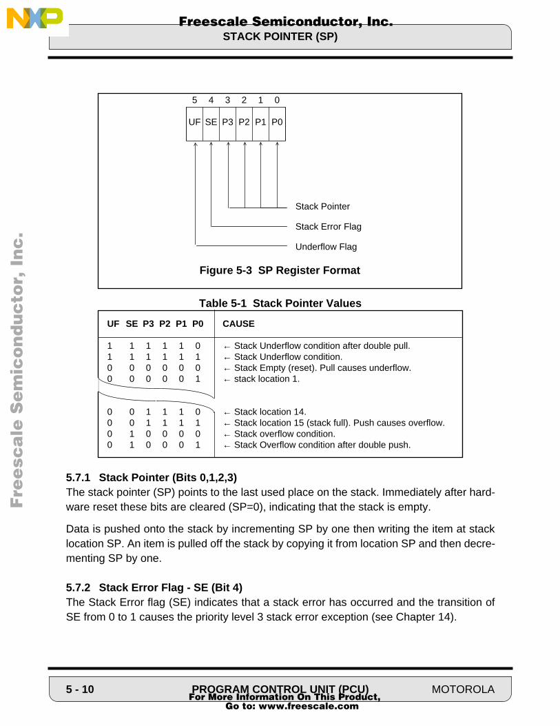
STACK POINTER (SP)
Fre
esc
ale
Se
mic
on
du
cto
r, I
Freescale Semiconductor, Inc.n
c..
.
Table 5-1 Stack Pointer Values
5.7.1 Stack Pointer (Bits 0,1,2,3)The stack pointer (SP) points to the last used place on the stack. Immediately after hard-ware reset these bits are cleared (SP=0), indicating that the stack is empty.
Data is pushed onto the stack by incrementing SP by one then writing the item at stacklocation SP. An item is pulled off the stack by copying it from location SP and then decre-menting SP by one.
5.7.2 Stack Error Flag - SE (Bit 4)The Stack Error flag (SE) indicates that a stack error has occurred and the transition ofSE from 0 to 1 causes the priority level 3 stack error exception (see Chapter 14).
5 4 3 2 1 0
Stack Pointer
Stack Error Flag
Underflow Flag
UF SE P3 P2 P1 P0
Figure 5-3 SP Register Format
UF SE P3 P2 P1 P0 CAUSE
1 1 1 1 1 0 ← Stack Underflow condition after double pull.1 1 1 1 1 1 ← Stack Underflow condition.0 0 0 0 0 0 ← Stack Empty (reset). Pull causes underflow.0 0 0 0 0 1 ← stack location 1. 0 0 1 1 1 0 ← Stack location 14. 0 0 1 1 1 1 ← Stack location 15 (stack full). Push causes overflow.0 1 0 0 0 0 ← Stack overflow condition. 0 1 0 0 0 1 ← Stack Overflow condition after double push.
5 - 10 PROGRAM CONTROL UNIT (PCU) MOTOROLA For More Information On This Product,
Go to: www.freescale.com
STACK POINTER (SP)
Fre
esc
ale
Se
mic
on
du
cto
r, I
Freescale Semiconductor, Inc.n
c..
.
When the stack is completely full, the Stack pointer reads 001111, and any operationthat pushes data to the stack will cause a stack error exception to occur and the stackregister will read 010000 (or 010001 if an implied double push occurs).
Any implied pull operation with SP=0 will cause a Stack Error exception (See chapter14), and the SP will read all ones (or 111110 if an implied double pull occurs). As shownin Figure 5-4, the SE bit is set.
Note: When SP=0 (stack empty), instructions which read stack without SP post-decre-ment and instructions which write stack without SP pre-increment do not cause astack error exception. i.e. DO SSL, xxxx; REP SSL; MOVEC or MOVEP when SSLis specified as a source or destination.
5.7.3 Underflow Flag - UF (Bit 5)The Underflow flag (UF) is set when a stack underflow occurs. See Figure 5-4.
When the user explicitly writes the SP register with the UF set and the SE cleared, andfollows this operation with an implicit stack operation that increments/decrements thestack pointer, the Underflow flag will be cleared by the implicit operation. As long as theSE was not set. If the Stack Error was set, the Underflow flag will not change state (the“sticky” effect). In this way, when a stack error does occur, the reason for the error,underflow or overflow, is preserved. Some examples are given below as illustrations:
Example 1:move #$20,sp ; set underflow flag, clear stack error flagmove anything,ssh ; implicit SP incrementmove sp,x:out ; read SP, it should be $01
In this example, the implicit SP increment cleared the Underflow flag because the StackError flag was cleared.
Example 2:move #$30,sp ; set underflow flag, set stack error flagmove anything,ssh ; implicit SP incrementmove sp,x:out ; read SP, it should be $31
In this example, the implicit SP increment did not clear the UF because SE was set.
Example 3:move #$2F,sp ; set underflow flag, clear stack error flagmove anything,ssh ; implicit SP incrementmove sp,x:out ; read SP, it should be $10
MOTOROLA PROGRAM CONTROL UNIT (PCU) 5 - 11 For More Information On This Product,
Go to: www.freescale.com
OPERATING MODE REGISTER (OMR)
Fre
esc
ale
Se
mic
on
du
cto
r, I
Freescale Semiconductor, Inc.n
c..
.
In this example, the implicit SP increment produced a stack overflow error, setting StackError and clearing the Underflow flag (to show an overflow error).
While the Stack Error flag is set, implicit SP increments/decrements will not affect theUnderflow or Stack Error flags in any way (this is the “sticky” effect) even if decrementingwhen the 4 LSBs of SP are’0’ or incrementing when the 4 LSBs of SP are’1’.
Example 4:move #$10,sp ; clear underflow flag, set stack error flagmove ssh,destin. ; implicit SP decrementmove sp,x:out ; read SP, it should be $1F
In this example, the implicit SP decrement did not set the Underflow flag to denoteunderflow because the Stack Error flag was set.
Example 5:move #$3F,sp ; set underflow flag, set stack error flagmove anything,ssh ; implicit SP incrementmove sp,x:out ; read SP, it should be $30
In this example, the implicit SP increment did not clear the Underflow flag to denote over-flow because the Stack Error flag was set.
5.7.4 Unimplemented Stack Pointer Register bitsAny unimplemented stack pointer register bits are reserved for future expansion and willread as zero during DSP read operations.
5.8 OPERATING MODE REGISTER (OMR)The operating mode register (OMR) is a 16-bit register which defines the current chipoperating mode of the processor. The OMR bits are only affected by processor reset andby instructions which directly reference the OMR.
During processor reset the chip operating mode bits will be loaded from the externalMode Select pins. The operating mode register format is shown in Figure 5-4 and isdescribed below.
Note: When a bit of the OMR is changed by an instruction, a delay of one instruction cycleis necessary before the new mode comes into effect.
5 - 12 PROGRAM CONTROL UNIT (PCU) MOTOROLA For More Information On This Product,
Go to: www.freescale.com
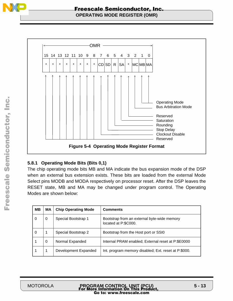
OPERATING MODE REGISTER (OMR)
Fre
esc
ale
Se
mic
on
du
cto
r, I
Freescale Semiconductor, Inc.n
c..
.
5.8.1 Operating Mode Bits (Bits 0,1)The chip operating mode bits MB and MA indicate the bus expansion mode of the DSPwhen an external bus extension exists. These bits are loaded from the external ModeSelect pins MODB and MODA respectively on processor reset. After the DSP leaves theRESET state, MB and MA may be changed under program control. The OperatingModes are shown below:
15 14 13 12 11 10 9 8 7 6 5 4 3 2 1 0
OMR
Operating ModeBus Arbitration Mode
ReservedSaturation RoundingStop DelayClockout DisableReserved
* * * * * * * * CD SD R SA * MC MB MA
Figure 5-4 Operating Mode Register Format
MB MA Chip Operating Mode Comments
0 0 Special Bootstrap 1 Bootstrap from an external byte-wide memorylocated at P:$C000.
0 1 Special Bootstrap 2 Bootstrap from the Host port or SSI0
1 0 Normal Expanded Internal PRAM enabled; External reset at P:$E0000
1 1 Development Expanded Int. program memory disabled; Ext. reset at P:$000.
MOTOROLA PROGRAM CONTROL UNIT (PCU) 5 - 13 For More Information On This Product,
Go to: www.freescale.com

OPERATING MODE REGISTER (OMR)
Fre
esc
ale
Se
mic
on
du
cto
r, I
Freescale Semiconductor, Inc.n
c..
.
5.8.2 Bus Arbitration Mode Bit (Bit 2)The bus operating mode bit MC indicates the bus arbitration mode of the DSP when anexternal bus extension exists. This bit is loaded from the external Mode Select pinMODC on processor reset. After the DSP leaves the RESET state, MC may be changedunder program control. The Bus Operating Modes are shown below and more details aregiven in Section 7 and Section 15.
5.8.3 Saturation Bit (Bit 4)The Saturation bit (SA), when set, selects automatic saturation on 32 bits for the resultsgoing to the accumulator. This saturation is done by a special saturation circuit inside theMAC unit. The purpose of this bit is to provide a saturation mode for 16-bit algorithmswhich do not recognize or cannot take advantage of the extension accumulator.
The saturation logic operates by checking three bits of the 40-bit result: two bits of theextension byte (exp[7] and exp[0]) and one bit on the MSP (msp[15]). The resultobtained in the accumulator when SA =1 is shown in Table 5-2:
Table 5-2 Actions of the Saturation Mode (SA=1)
This bit is cleared by processor reset.
The scaling bits are ignored by this saturation logic and the two saturation constants$007FFFFFFF and $FF80000000 are not affected by the scaling mode. In the sameway, the rounding of the saturation constant (during MPYR, MACR, RND) is independentof the scaling mode: $007FFFFFFF is rounded to $007FFF0000 and $FF80000000 to$FF80000000.
MC Bus Arbitration Mode
0 Slave1 Master
exp[7] exp[0] msp[15] result in accumulator
0 0 0 unchanged0 0 1 $00 7FFF FFFF0 1 0 $00 7FFF FFFF0 1 1 $00 7FFF FFFF
1 0 0 $FF 8000 00001 0 1 $FF 8000 00001 1 0 $FF 8000 00001 1 1 unchanged
5 - 14 PROGRAM CONTROL UNIT (PCU) MOTOROLA For More Information On This Product,
Go to: www.freescale.com

OPERATING MODE REGISTER (OMR)
Fre
esc
ale
Se
mic
on
du
cto
r, I
Freescale Semiconductor, Inc.n
c..
.
CAUTIONThe saturation mode is ALWAYS disabled during the execution of the fol-lowing instructions: DMACsu, DMACuu, MACsu, MACuu, MPYsu, MPYuu,and ASL4. The instruction ASL4 A (or B) can be followed by a MOVE A,A(or B,B) for proper operation when the saturation mode is turned on. How-ever, the “V” bit of the status register will never be set by the saturation ofthe accumulator during the MOVE A,A (or B,B). Only the “L” bit will then beset. If the “V” bit needs to be tested by the program, ASL4 has to be substi-tuted by a repetition of four ASLs.
5.8.4 Rounding Bit (Bit 5)The Rounding bit (R)selects between convergent rounding and twos-complement round-ing. When set, two’s-complement rounding (always round up) is used.
This bit is cleared by processor reset.
5.8.5 Stop Delay Bit (Bit 6)The Stop Delay bit (SD) is used to select the delay that the DSP needs to exit the STOPmode. Refer to Section 7.5 for more details.
This bit is cleared by processor reset.
5.8.6 Clock Out Disable Bit (Bit 7)When the Clock out Disable bit (CD) is cleared in the OMR, a clock out signal comes outof the CLKO pin. Setting the CD bit will disable the signal coming out of the CLKO pinone instruction cycle after the bit has been set. This bit can be set by the user programwhen radiation sensitive applications do not need the clock out signal.
This bit is cleared by processor reset.
5.8.7 Reserved Operating Mode Register Bits (Bits 3 and 8-15)These operating mode register bits are reserved. They will read as zero during DSP readoperations and should be written as zero to ensure future compatibility.
MOTOROLA PROGRAM CONTROL UNIT (PCU) 5 - 15 For More Information On This Product,
Go to: www.freescale.com

OPERATING MODE REGISTER (OMR)
F
ree
sca
le S
em
ico
nd
uc
tor,
I
Freescale Semiconductor, Inc.n
c..
.
5 - 16 PROGRAM CONTROL UNIT (PCU) MOTOROLA For More Information On This Product,
Go to: www.freescale.com

Fre
esc
ale
Se
mic
on
du
cto
r, I
Freescale Semiconductor, Inc.n
c..
.
SECTION 6
INSTRUCTION SET AND EXECUTION
Fetch F1 F2 F3 F3e F4 F5 F6 …Decode D1 D2 D3 D3e D4 D5 …Execute E1 E2 E3 E3e E4 …InstructionCycle: 1 2 3 4 5 6 7 …
MOTOROLA INSTRUCTION SET AND EXECUTION 6 - 1 For More Information On This Product,
Go to: www.freescale.com

SECTION CONTENTS
Fre
esc
ale
Se
mic
on
du
cto
r, I
Freescale Semiconductor, Inc.n
c..
.
6.1 INTRODUCTION . . . . . . . . . . . . . . . . . . . . . . . . . . . . . . . . . . . . . . . . 6-36.2 INSTRUCTION GROUPS . . . . . . . . . . . . . . . . . . . . . . . . . . . . . . . . . . 6-36.2.1 Arithmetic Instructions . . . . . . . . . . . . . . . . . . . . . . . . . . . . . . . . . . . . . 6-36.2.2 Logical Instructions . . . . . . . . . . . . . . . . . . . . . . . . . . . . . . . . . . . . . . . 6-46.2.3 Bit Field Manipulation Instructions . . . . . . . . . . . . . . . . . . . . . . . . . . . 6-56.2.4 Loop Instructions . . . . . . . . . . . . . . . . . . . . . . . . . . . . . . . . . . . . . . . . . 6-56.2.5 Move Instructions . . . . . . . . . . . . . . . . . . . . . . . . . . . . . . . . . . . . . . . . 6-66.2.6 Program Control Instructions . . . . . . . . . . . . . . . . . . . . . . . . . . . . . . . 6-66.3 INSTRUCTION FORMATS . . . . . . . . . . . . . . . . . . . . . . . . . . . . . . . . . 6-66.4 INSTRUCTION EXECUTION . . . . . . . . . . . . . . . . . . . . . . . . . . . . . . . 6-76.4.1 Instruction Processing . . . . . . . . . . . . . . . . . . . . . . . . . . . . . . . . . . . . . 6-76.4.2 Memory Access Processing . . . . . . . . . . . . . . . . . . . . . . . . . . . . . . . . 6-8
6 - 2 INSTRUCTION SET AND EXECUTION MOTOROLA For More Information On This Product,
Go to: www.freescale.com

INTRODUCTION
Fre
esc
ale
Se
mic
on
du
cto
r, I
Freescale Semiconductor, Inc.n
c..
.
6.1 INTRODUCTIONAs indicated by the programming model in Chapter 5, the DSP architecture can beviewed as three functional units operating in parallel (Data ALU, AGU and PCU). Thegoal of the instruction set is to keep each of these units busy each instruction cycle. Thisachieves maximum speed and minimum use of program memory.
This section introduces the DSP instruction set and instruction format. The completerange of instruction capabilities combined with the flexible addressing modes provide avery powerful assembly language for digital signal processing algorithms. The instructionset has also been designed to allow efficient coding for future high-level DSP languagecompilers. Execution time is enhanced by the hardware looping capabilities.
6.2 INSTRUCTION GROUPSThe instruction set is divided into the following groups:
• Arithmetic• Logical• Bit Field Manipulation• Loop• Move• Program Control
Each instruction group is described in the following sections. Detailed information oneach instruction is given in Appendix A.
6.2.1 Arithmetic InstructionsThe arithmetic instructions perform all of the arithmetic operations within the Data ALU.They may affect all of the condition code register bits. Arithmetic instructions are register-based (register direct addressing modes used for operands) so that the Data ALU opera-tion indicated by the instruction does not use the XDB or the GDB. Optional data trans-fers may be specified with most arithmetic instructions. This allows for parallel datamovement over the XDB and over the GDB during a Data ALU operation. This allowsnew data to be prefetched for use in following instructions and results calculated by pre-vious instructions to be stored. These instructions execute in one instruction cycle. Thefollowing are the arithmetic instructions.
ABS Absolute ValueADC Add Long with CarryADD AddASL Arithmetic Shift LeftASL4 4 Bit Arithmetic Shift Left*ASR Arithmetic Shift Right
MOTOROLA INSTRUCTION SET AND EXECUTION 6 - 3 For More Information On This Product,
Go to: www.freescale.com

INSTRUCTION GROUPS
Fre
esc
ale
Se
mic
on
du
cto
r, I
Freescale Semiconductor, Inc.n
c..
.
ASR4 4 Bit Arithmetic Shift Right*ASR16 16 Bit Arithmetic Shift Right*CLR Clear an AccumulatorCLR24 Clear 24 MSBs of an AccumulatorCMP CompareCMPM Compare MagnitudeDEC Decrement AccumulatorDEC24 Decrement upper word of AccumulatorDIV Divide Iteration*DMAC Double (Multi) precision oriented MAC*EXT Sign Extend Accumulator from bit 31*IMAC Integer Multiply-Accumulate*IMPY Integer Multiply*INC Increment AccumulatorINC24 Increment 24 MSBs of AccumulatorMAC Signed Multiply-AccumulateMACR Signed Multiply-Accumulate and RoundMPY Signed MultiplyMPYR Signed Multiply and RoundMPY(su,uu) Mixed mode Multiply*MAC(su,uu) Mixed mode Multiply-Accumulate*NEG NegateNEGC Negate with Borrow*NORM Normalize*RND RoundSBC Subtract Long with CarrySUB SubtractSUBL Shift Left and SubtractSWAP Swap MSP and LSP of an Accumulator*Tcc Transfer Conditionally*TFR Transfer Data ALU Register (Accumulator as destination)TFR2 Transfer Accumulator (32 bit Data Alu register as destination)*TST Test an accumulatorTST2 Test an ALU data register*ZERO Zero Extend Accumulator from bit 31*
*These instructions do not allow parallel data moves.
6.2.2 Logical InstructionsThe logical instructions perform all of the logical operations within the Data ALU. Theymay affect all of the condition code register bits. Logical instructions are register-basedas are the arithmetic instructions above. Optional data transfers may be specified withmost logical instructions. This allows for parallel data movement over the XDB and overthe GDB during a Data ALU operation. This allows new data to be prefetched for use infollowing instructions and results calculated in previous instructions to be stored. Withthe exceptions of ANDI or ORI the destination of all logical instructions is A1 or B1.
6 - 4 INSTRUCTION SET AND EXECUTION MOTOROLA For More Information On This Product,
Go to: www.freescale.com

INSTRUCTION GROUPS
Fre
esc
ale
Se
mic
on
du
cto
r, I
Freescale Semiconductor, Inc.n
c..
.
These instructions execute in one instruction cycle. The following are the logical instruc-tions.
AND Logical ANDANDI AND Immediate Program Controller Register*EOR Logical Exclusive ORLSL Logical Shift LeftLSR Logical Shift RightNOT Logical ComplementOR Logical Inclusive ORORI OR Immediate Program Controller Register*ROL Rotate LeftROR Rotate Right
*These instructions do not allow parallel data moves.
6.2.3 Bit Field Manipulation InstructionsThis group tests the state of any set of bits within a byte in a memory location or a regis-ter and then sets, clears, or inverts bits in this byte. Bit fields which can be tested includethe upper byte and the lower byte in a 16 bit value. The carry bit of the condition coderegister will contain the result of the bit test for each instruction. These instructions areread-modify-write type operations and require two instruction cycles. The following arethe bit field manipulation instructions.
BFTSTL Bit Field Test LowBFTSTH Bit Field Test HighBFCLR Bit Field Test and ClearBFSET Bit Field Test and SetBFCHG Bit Field Test and Change
6.2.4 Loop InstructionsThe loop instructions control hardware looping by initiating a program loop and setting uplooping parameters, or by “cleaning” up the system stack when terminating a loop. Initial-ization includes saving registers used by a program loop (LA and LC) on the systemstack so that program loops can be nested. The address of the first instruction in a pro-gram loop is also saved to allow no-overhead looping. The end address of the DO loop isspecified as PC relative. The following are the loop instructions.
DO Start Hardware LoopDO FOREVER Hardware Loop for everENDDO Disable Current Loop and Unstack Parameters BRKcc Conditional Exit from Hardware Loop
MOTOROLA INSTRUCTION SET AND EXECUTION 6 - 5 For More Information On This Product,
Go to: www.freescale.com

INSTRUCTION FORMATS
Fre
esc
ale
Se
mic
on
du
cto
r, I
Freescale Semiconductor, Inc.n
c..
.
6.2.5 Move InstructionsThe move instructions perform data movement over the XDB and over the GDB. Moveinstructions do not affect the condition code register except the limit bit L if limiting is per-formed when reading a Data ALU accumulator register. AGU instructions are alsoincluded among the following move instructions. These instructions do not allow optionaldata transfers. In addition to the following move instructions, there are parallel moveswhich can be used simultaneously with many of the other instructions.
LEA Load Effective AddressMOVE Move Data with or without register transfer – TFR(3)MOVE(C) Move Control Register MOVE(I) Move Immediate ShortMOVE(M) Move Program MemoryMOVE(P) Move Peripheral DataMOVE(S) Move Absolute Short
6.2.6 Program Control InstructionsThe program control instructions include branches, jumps, conditional branches andjumps and other instructions which affect the PC and system stack. Program controlinstructions may affect the condition code register bits as specified in the instruction.The following are the program control instructions.
Bcc Branch ConditionallyBSR Branch to Subroutine (PC relative)BRA BranchBScc Branch to Subroutine ConditionallyDEBUG Enter Debug ModeDEBUGcc Enter Debug Mode ConditionallyJcc Jump ConditionallyJMP JumpJSR Jump to SubroutineJScc Jump to Subroutine Conditionally
NOP No OperationREP Repeat Next InstructionREPcc Repeat Next Instruction ConditionallyRESET Reset Peripheral DevicesRTI Return from InterruptRTS Return from SubroutineSTOP Stop Processing (low power stand-by)SWI Software InterruptWAIT Wait for Interrupt (low power stand-by)
6.3 INSTRUCTION FORMATSInstructions are one or two words in length. The instruction and its length are specified bythe first word of the instruction. The next word may contain information about the instruc-tion itself or about an operand for the instruction. The assembly language source code
6 - 6 INSTRUCTION SET AND EXECUTION MOTOROLA For More Information On This Product,
Go to: www.freescale.com
INSTRUCTION EXECUTION
Fre
esc
ale
Se
mic
on
du
cto
r, I
Freescale Semiconductor, Inc.n
c..
.
for a typical one word instruction is shown below. The source code is organized into fourcolumns.
Opcode Operands X Bus Data G Bus DataMAC X0,Y0,A X:(R0)+,X0 X:(R3)+,Y0
The Opcode column indicates the Data ALU, AGU, or PCU operation to be performed.The Operands column specifies the operands to be used by the opcode. The X Bus Dataand G Bus Data columns specify optional data transfers over the X Bus and the address-ing modes to be used. The Opcode column must always be included in the source code.
The DSP offers parallel processing using the Data ALU, AGU and PCU. For the instruc-tion word above, the DSP will perform the designated ALU operation (Data ALU), up totwo data transfers specified with address register updates (AGU), and will also decodethe next instruction and fetch an instruction from program memory (PCU) all in oneinstruction cycle. When an instruction is more than one word in length, an additionalinstruction execution cycle is required. Most instructions involving the Data ALU are reg-ister-based (all operands are in Data ALU registers) and allow the programmer to keepeach parallel processing unit busy. An instruction which is memory-oriented (such as abit field manipulation instruction) or that causes a control flow change (such as a branch/jump) prevents the use of parallel processing resources during its execution.
6.4 INSTRUCTION EXECUTIONInstruction execution is pipelined to allow most instructions to execute at a rate of oneinstruction every clock cycle. However, certain instructions will require additional time toexecute. These include instructions which are longer than one word, instructions whichuse an addressing mode that requires more than one cycle, instructions which make useof the global data bus more than once, and instructions which cause a control flowchange. In the latter case a cycle is needed to clear the pipeline.
6.4.1 Instruction ProcessingPipelining allows the fetch-decode-execute operations of an instruction to occur duringthe fetch-decode-execute operations of other instructions. While an instruction is exe-cuted, the next instruction to be executed is decoded, and the instruction to follow theinstruction being decoded is fetched from program memory. If an instruction is two wordsin length, the additional word will be fetched before the next instruction is fetched. Theillustration below demonstrates pipelining; F1, D1 and E1 refer to the fetch, decode andexecute operations, respectively, of the first instruction. Note, the third instruction con-tains an instruction extension word and takes two cycles to execute.
MOTOROLA INSTRUCTION SET AND EXECUTION 6 - 7 For More Information On This Product,
Go to: www.freescale.com
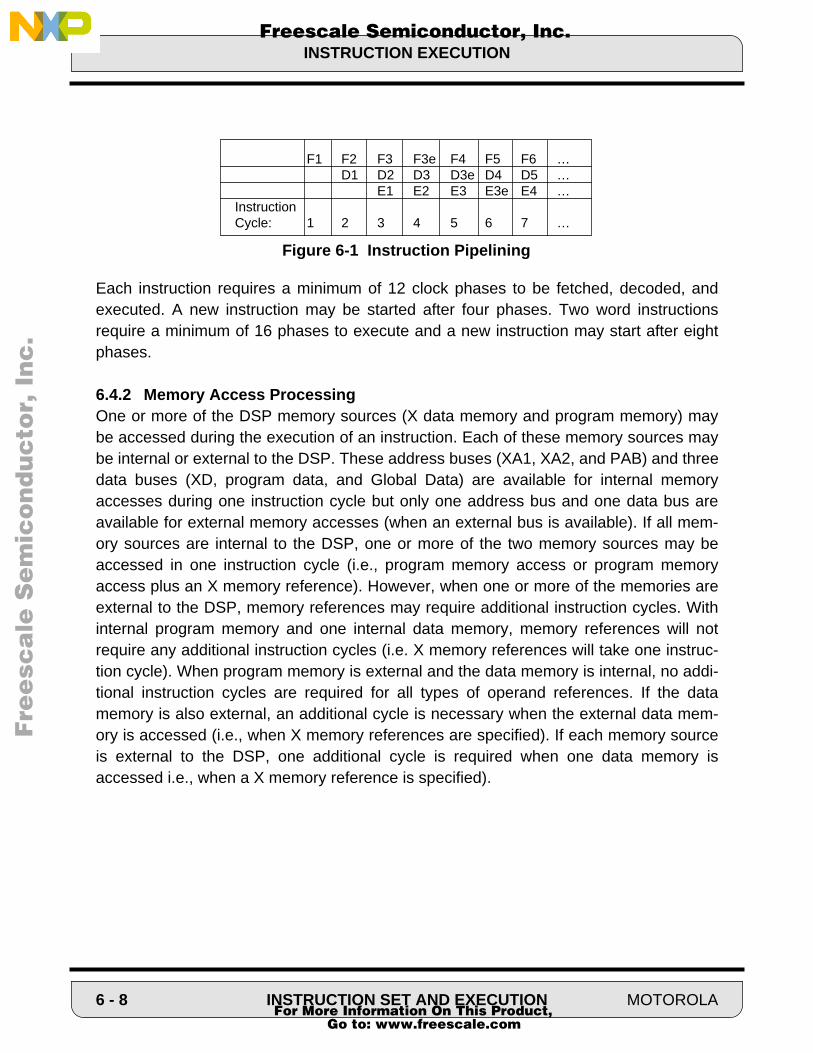
INSTRUCTION EXECUTION
Fre
esc
ale
Se
mic
on
du
cto
r, I
Freescale Semiconductor, Inc.n
c..
.
Each instruction requires a minimum of 12 clock phases to be fetched, decoded, andexecuted. A new instruction may be started after four phases. Two word instructionsrequire a minimum of 16 phases to execute and a new instruction may start after eightphases.
6.4.2 Memory Access ProcessingOne or more of the DSP memory sources (X data memory and program memory) maybe accessed during the execution of an instruction. Each of these memory sources maybe internal or external to the DSP. These address buses (XA1, XA2, and PAB) and threedata buses (XD, program data, and Global Data) are available for internal memoryaccesses during one instruction cycle but only one address bus and one data bus areavailable for external memory accesses (when an external bus is available). If all mem-ory sources are internal to the DSP, one or more of the two memory sources may beaccessed in one instruction cycle (i.e., program memory access or program memoryaccess plus an X memory reference). However, when one or more of the memories areexternal to the DSP, memory references may require additional instruction cycles. Withinternal program memory and one internal data memory, memory references will notrequire any additional instruction cycles (i.e. X memory references will take one instruc-tion cycle). When program memory is external and the data memory is internal, no addi-tional instruction cycles are required for all types of operand references. If the datamemory is also external, an additional cycle is necessary when the external data mem-ory is accessed (i.e., when X memory references are specified). If each memory sourceis external to the DSP, one additional cycle is required when one data memory isaccessed i.e., when a X memory reference is specified).
F1 F2 F3 F3e F4 F5 F6 …D1 D2 D3 D3e D4 D5 …
E1 E2 E3 E3e E4 …InstructionCycle: 1 2 3 4 5 6 7 …
Figure 6-1 Instruction Pipelining
6 - 8 INSTRUCTION SET AND EXECUTION MOTOROLA For More Information On This Product,
Go to: www.freescale.com

Fre
esc
ale
Se
mic
on
du
cto
r, I
Freescale Semiconductor, Inc.n
c..
.
SECTION 7
PROCESSING STATES
STOP
WAIT
EXCEPTION
NORMAL
RESET
MOTOROLA PROCESSING STATES 7 - 1 For More Information On This Product,
Go to: www.freescale.com

SECTION CONTENTS
Fre
esc
ale
Se
mic
on
du
cto
r, I
Freescale Semiconductor, Inc.n
c..
.
7.1 INTRODUCTION . . . . . . . . . . . . . . . . . . . . . . . . . . . . . . . . . . . . . . . . 7-37.2 NORMAL PROCESSING STATE . . . . . . . . . . . . . . . . . . . . . . . . . . . . 7-37.2.1 Instruction Pipeline . . . . . . . . . . . . . . . . . . . . . . . . . . . . . . . . . . . . . . . 7-37.2.2 Summary of Pipeline Related Restrictions . . . . . . . . . . . . . . . . . . . . . 7-87.2.2.1 DO Instruction Restrictions . . . . . . . . . . . . . . . . . . . . . . . . . . . . . . . . . 7-87.2.2.2 Restrictions Near the End of DO Loops . . . . . . . . . . . . . . . . . . . . . . . 7-87.2.2.3 ENDDO Instruction Restrictions . . . . . . . . . . . . . . . . . . . . . . . . . . . . . 7-97.2.2.4 RTI and RTS Instruction Restrictions . . . . . . . . . . . . . . . . . . . . . . . . . 7-97.2.2.5 SP and SSH/SSL Register Manipulation Restrictions . . . . . . . . . . . . 7-97.2.2.6 Rn, Nn, and Mn Register Restrictions . . . . . . . . . . . . . . . . . . . . . . . . . 7-97.2.2.7 Fast Interrupt Routine Restrictions . . . . . . . . . . . . . . . . . . . . . . . . . . . 7-107.3 EXCEPTION PROCESSING (INTERRUPT PROCESSING) . . . . . . . 7-107.3.1 Interrupt Types . . . . . . . . . . . . . . . . . . . . . . . . . . . . . . . . . . . . . . . . . . 7-127.3.2 Interrupt Arbitration . . . . . . . . . . . . . . . . . . . . . . . . . . . . . . . . . . . . . . . 7-127.3.3 Interrupt Instruction Fetch . . . . . . . . . . . . . . . . . . . . . . . . . . . . . . . . . . 7-137.3.4 Interrupt Instruction Execution . . . . . . . . . . . . . . . . . . . . . . . . . . . . . . 7-137.3.4.1 Fast Interrupt . . . . . . . . . . . . . . . . . . . . . . . . . . . . . . . . . . . . . . . . . . . . 7-147.3.4.2 Long Interrupt . . . . . . . . . . . . . . . . . . . . . . . . . . . . . . . . . . . . . . . . . . . 7-157.3.4.3 Case of the REP Instruction . . . . . . . . . . . . . . . . . . . . . . . . . . . . . . . . 7-167.3.5 Interrupt Sources . . . . . . . . . . . . . . . . . . . . . . . . . . . . . . . . . . . . . . . . 7-167.3.5.1 Hardware Interrupt Sources . . . . . . . . . . . . . . . . . . . . . . . . . . . . . . . . 7-177.3.5.2 Software Interrupt Sources . . . . . . . . . . . . . . . . . . . . . . . . . . . . . . . . . 7-207.3.5.3 Stack Error Interrupt . . . . . . . . . . . . . . . . . . . . . . . . . . . . . . . . . . . . . . 7-227.3.6 Interrupt Priority Structure . . . . . . . . . . . . . . . . . . . . . . . . . . . . . . . . . . 7-227.3.6.1 Interrupt Priority Levels (IPL) . . . . . . . . . . . . . . . . . . . . . . . . . . . . . . . 7-237.3.6.2 Exception Priorities within an IPL . . . . . . . . . . . . . . . . . . . . . . . . . . . . 7-247.4 RESET STATE PROCESSING . . . . . . . . . . . . . . . . . . . . . . . . . . . . . 7-247.5 WAIT STATE PROCESSING . . . . . . . . . . . . . . . . . . . . . . . . . . . . . . . 7-257.6 STOP STATE PROCESSING . . . . . . . . . . . . . . . . . . . . . . . . . . . . . . . 7-28
7 - 2 PROCESSING STATES MOTOROLA For More Information On This Product,
Go to: www.freescale.com
INTRODUCTION
Fre
esc
ale
Se
mic
on
du
cto
r, I
Freescale Semiconductor, Inc.n
c..
.
7.1 INTRODUCTIONThe DSP56100 family is always in one of five processing states: normal, exception,reset, wait, and stop. These states are described in the following paragraphs.
7.2 NORMAL PROCESSING STATEThe normal processing state is associated with instruction execution. Details on normalprocessing of the individual instructions can be found in Appendix A. Instructions areexecuted using a three stage pipeline which is described in the following paragraphs.
7.2.1 Instruction PipelineThe 16-bit DSP instruction execution is performed in a three level pipeline allowing mostinstructions to execute at a rate of one instruction every instruction cycle. However, cer-tain instructions will require additional time to execute. These include instructions whichare longer than one word, instructions which use an addressing mode that requires morethan one cycle, and instructions which cause a control flow change. In the latter case acycle is needed to clear the pipeline.
Instruction pipelining allows overlapping the execution of instructions such that the fetch-decode-execute operations of a given instruction occurs concurrently with the fetch-decode-execute operations of other instructions. Specifically, while an instruction is exe-cuted, the next instruction to be executed is decoded, and the instruction to follow theinstruction being decoded is fetched from program memory. Only one word is fetchedper cycle so that if an instruction is two words in length, the additional word will befetched before the next instruction is fetched. Figure 7-1 demonstrates pipelining. F1,D1, and E1 refer to the fetch, decode, and execute operations, respectively, of the firstinstruction. The third instruction contains an instruction extension word and takes twoinstruction cycles to execute. Although it takes three instruction cycles for the pipeline tofill and the first instruction to execute, an instruction usually executes on each instructioncycle thereafter.
Summarizing; each instruction requires a minimum of 3 instruction cycles (12 clockphases) to be fetched, decoded, and executed. This means that there is a delay of threeinstruction cycles on power up to fill the pipe. A new instruction may be started immedi-ately following the previous instruction. Two word instructions require a minimum of fourinstruction cycles to execute (three cycles for the first instruction word to move throughthe pipe and execute and one more for the second word to execute) and a new instruc-tion may start after the second cycle of the preceding instruction.
MOTOROLA PROCESSING STATES 7 - 3 For More Information On This Product,
Go to: www.freescale.com

NORMAL PROCESSING STATE
Fre
esc
ale
Se
mic
on
du
cto
r, I
Freescale Semiconductor, Inc.n
c..
.
Figure 7-1 Instruction Pipelining
The pipeline is normally transparent to the user. However, it will affect program executionin some situations. These situations are instruction sequence dependent and are bestdescribed by case studies. Most of these restricted sequences occur because (1) alladdresses are formed during instruction decode or (2) contention for an internal resourcesuch as the status register (SR) occurs. If the execution of an instruction depends on therelative location of the instruction in a sequence of instructions, there is a pipeline effect.To test for a suspected pipeline effect, compare between the execution of the suspectinstruction (1) when it directly follows the previous instruction and (2) when four NOPsare inserted between the two. If there is a difference, it is due to a pipeline effect. The 16-bit DSP assembler is designed to flag instruction sequences with potential pipelineeffects so that the user can decide if the operation will be as expected.
Case 1: The following two examples show similar code sequences, the first with no pipe-line effect and the second with a pipeline effect.
1) No pipeline effect:
ORI #xx,CCR ;Changes CCR at the end of execution time slot
Jcc xxxx ;Reads condition codes in SR in its execution time slot
The Jcc will test the bits modified by the ORI without any pipeline effect in the code seg-ment above.
2) Instruction which started execution during decode:
ORI #03,OMR ;Sets MA, MB bits at execution time slot
MOVE x:$100,a ;Reads internal RAM instead of external RAM
There is a pipeline effect in example 2 because the address of the move is formed at itsdecode time before the ORI changes the MA and MB bits (which change the memorymap) in the ORI’s execution time slot. The following code produces the expected resultsof reading the external RAM:
ORI #03,OMR ;Sets MA, MB bits at execution time slot NOP ;Delays the MOVE so it will read the updated OMR MOVE x:$100,a ;Reads external RAM
Case 2: One of the more common sequences where pipeline effects are apparent is:
Instruction Cycle 1 2 3 4 5 6 7 . . .
Fetch F1 F2 F3 F3e F4 F5 F6 . . . Decode D1 D2 D3 D3e D4 D5 . . . Execute E1 E2 E3 E3e E4 . . .
7 - 4 PROCESSING STATES MOTOROLA For More Information On This Product,
Go to: www.freescale.com

NORMAL PROCESSING STATE
Fre
esc
ale
Se
mic
on
du
cto
r, I
Freescale Semiconductor, Inc.n
c..
.
. .MOVE #xxxx,Rn ;Move a number into register Rn (n=0-7).MOVE X:(Rn),A ;Use the new contents of Rn to address memory. . .
In this case, before the first MOVE instruction has written Rn during its execution cycle,the second MOVE has accessed the old Rn and therefore will use the old contents of Rn.This is because the address for indirect moves is formed during the decode cycle. Thisoverlapping instruction execution in the pipeline causes the pipeline effect. One instruc-tion cycle should be allowed after a register has been written by a MOVE instructionbefore the new contents are available for use by another MOVE instruction. The properinstruction sequence is:
. . MOVE X0,Rn ;Move a number into register Rn. NOP ;Execute any instruction or instruction sequence not using Rn . .MOVE X:(Rn),A ;Use the new contents of Rn.
Case 3: A situation related to Case 2 can be seen in the boot ROM program. At the endof the bootstrap operation, the OMR is changed to Mode #2 and then the program thatwas loaded is executed. This process is accomplished in the last three instructions whichare shown below:
_BOOTENDMOVEC #2,OMR ; Set the operating mode to 2
; (and trigger an exit from; bootstrap mode).
ANDI #$0,CCR ; Clear SR as if RESET and ; introduce delay needed for; Op. Mode change.
JMP <$0 ; Start fetching from PRAM, P:$0000
The JMP instruction generates its jump address during its decode cycle. If the JMPinstruction followed the MOVEC, the MOVEC instruction would not have changed theOMR before the JMP instruction formed the fetch address. As a result, the jump wouldfetch the instruction at P:$0000 of the bootstrap ROM (MOVE #$FFC0,R2). The OMRwould then change due to the MOVEC instruction and the next instruction would be thesecond instruction of the downloaded code at P:$0001 of the internal RAM. However, theANDI instruction allows the OMR to be changed before the JMP instruction uses it andthe JMP fetches P:$0000 of the internal RAM as intended.
Case 4: An interrupt has two additional control cycles which are executed in the interruptcontroller concurrently with the fetch, decode, and execute cycles (see Section 7.3
MOTOROLA PROCESSING STATES 7 - 5 For More Information On This Product,
Go to: www.freescale.com

NORMAL PROCESSING STATE
Fre
esc
ale
Se
mic
on
du
cto
r, I
Freescale Semiconductor, Inc.n
c..
.
“Exception Processing” and Figure 7-2). During these two control cycles, the interrupt isarbitrated by comparing the interrupt mask level with the interrupt priority level (IPL) ofthe interrupt and either allowing or disallowing the interrupt. Therefore, if the interruptmask is changed after an interrupt is arbitrated and accepted as pending but before theinterrupt is executed, the interrupt will be executed regardless of what the mask waschanged to. The following examples show that the old interrupt mask is in effect forup to four additional instruction cycles after the interrupt mask is changed. Notethat all instructions shown in the examples here are one word instructions; however, onetwo-word instruction can replace two one-word instructions except where noted.
Program flow with no interrupts after interrupts are disabled:
. .ORI #03,MR ;disable interruptsINST 1INST 2INST 3INST 4
. .
Possible variations in program flow which may occur after interrupts are disabled:
. . . . . . . .ORI #03,MR ORI #03,MR ORI #03,MR ORI #03,MRII INST 1 INST 1 INST 1II+1 II INST 2 INST 2 INST 1 II+1 II INST 3 ← See note 1INST 2 INST 2 II+1 II INST 3 INST 3 INST 3 II+1INST 4 INST 4 INST 4 INST 4 . . . . . . . .
Note 1: INST 3 may be executed at that point only if the preceding instruction (INST 2)was a single-word instruction.
Note 2: II = Interrupt Instruction from maskable interrupt.
The following program flow WILL NOT occur because the ORI instruction becomeseffective after a pipeline latency of four instruction cycles:
7 - 6 PROCESSING STATES MOTOROLA For More Information On This Product,
Go to: www.freescale.com

NORMAL PROCESSING STATE
Fre
esc
ale
Se
mic
on
du
cto
r, I
Freescale Semiconductor, Inc.n
c..
.
. .ORI #03,MR ; Disable interrupts.INST 1INST 2INST 3INST 4
II ; Interrupts disabled. II+1 ; Interrupts disabled. .
.Program flow without interrupts after interrupts are re-enabled:
. .ANDI #00,MR ;enable interrupts INST 1 INST 2 INST 3 INST 4 . .
Program flow with interrupts after interrupts are re-enabled:
. .ANDI #00,MR ;Enable interruptsINST 1 ;UninterruptableINST 2 ;UninterruptableINST 3 ;II fetchedINST 4 ;II+1 fetchedIIII+1 . .
The DO instruction is another instruction which begins execution during the decode cycleof the pipeline. As a result, there are a number of restrictions concerning access conten-tion with the program controller registers which are accessed by the DO instruction. TheENDDO instruction has similar restrictions. Appendix A contains additional informationon the DO and ENDDO instruction restrictions.
Case 5: A resource contention problem can occur when one instruction is using a regis-ter during its decode while the instruction executing is accessing the same resource.One example of this is:
MOVEC X:$100,SSHDO #$10,END
The problem occurs because the MOVEC instruction loads the contents of X:$100 intothe SSH during T3 of its execute cycle. The DO instruction that follows pushes the stack
MOTOROLA PROCESSING STATES 7 - 7 For More Information On This Product,
Go to: www.freescale.com

NORMAL PROCESSING STATE
Fre
esc
ale
Se
mic
on
du
cto
r, I
Freescale Semiconductor, Inc.n
c..
.
(LA → SSH, LC → SSL) during T3 of its decode cycle. Therefore the two instructions trywriting to the SSH simultaneously and conflict.
7.2.2 Summary of Pipeline Related RestrictionsA summary of the instruction sequences that cause pipeline effects is given in the follow-ing paragraphs. Additional information concerning the individual instructions can befound in Appendix A.
7.2.2.1 DO Instruction RestrictionsThe DO instruction must not be immediately preceded by any of the following instruc-tions:
• BFCHG/BFCLR/BFSET LA, LC, SSH, SSL or SP • MOVEC/MOVEM to LA, LC, SSH, SSL or SP • MOVEC/MOVEM from SSH
7.2.2.2 Restrictions Near the End of DO LoopsProper DO loop operation is guaranteed if no instruction starting at address LA-2, LA-1or LA specifies the program controller registers SR, SP, SSL, LA, LC or (implicitly) PC asa destination register; or specifies SSH as a source or destination register. Also, SSHcan not be specified as a source register in the DO instruction itself.
These restricted instructions include:
- at LA-2, LA-1 and LA:
• DO • BFCHG/BFCLR/BFSET LA, LC, SR, SP, SSH, or SSL • BFTST SSH • MOVEC/MOVEM/MOVEP from SSH • MOVEC/MOVEM/MOVEP to LA, LC, SR, SP, SSH, or SSL• ANDI/ORI MR
- at LA:
• any two word instruction • Jcc, Bcc, JMP, BRA, JScc, BScc, JSR, BSR• REP, RESET, RTI, RTS, STOP, WAIT
Other restrictions:
• DO SSH,xxxx • JSR/JScc/BSR/BScc to (LA), if Loop Flag is set
7 - 8 PROCESSING STATES MOTOROLA For More Information On This Product,
Go to: www.freescale.com

NORMAL PROCESSING STATE
Fre
esc
ale
Se
mic
on
du
cto
r, I
Freescale Semiconductor, Inc.n
c..
.
7.2.2.3 ENDDO Instruction RestrictionsThe ENDDO instruction must not be immediately preceded by any of the followinginstructions:
• BFCHG/BFCLR/BFSET LA, LC, SR, SSH, SSL or SP • MOVEC/MOVEM to LA, LC, SR, SSH, SSL or SP • MOVEC/MOVEM from SSH • ANDI/ORI MR
7.2.2.4 RTI and RTS Instruction RestrictionsThe RTI instruction must not be immediately preceded by any of the following instruc-tions:
• BFCHG/BFCLR/BFSET SR, SSH, SSL or SP • MOVEC/MOVEM to SR, SSH, SSL or SP • MOVEC/MOVEM from SSH • ANDI MR, ANDI CCR • ORI MR, ORI CCR
The RTS instruction must not be immediately preceded by any of the following instruc-tions:
• BFCHG/BFCLR/BFSET SSH, SSL or SP • MOVEC/MOVEM to SSH, SSL or SP • MOVEC/MOVEM from SSH
7.2.2.5 SP and SSH/SSL Register Manipulation RestrictionsIn addition to all the above restrictions concerning SP, SSH, and SSL, the followinginstruction sequences are illegal:
• BFCHG/BFCLR/BFSET SP • MOVEC/MOVEM/MOVEP from SSH or SSL
and
• MOVEC/MOVEM to SP • MOVEC/MOVEM/MOVEP from SSH or SSL
Also the instruction MOVEC SSH,SSH is illegal.
7.2.2.6 Rn, Nn, and Mn Register RestrictionsIf an address register (R0-R3, N0-N3, or M0-M3) is changed with a move type instruction(LUA, Tcc, MOVE, MOVEM, MOVEC or parallel move), the new contents will not be
MOTOROLA PROCESSING STATES 7 - 9 For More Information On This Product,
Go to: www.freescale.com

EXCEPTION PROCESSING (INTERRUPT PROCESSING)
Fre
esc
ale
Se
mic
on
du
cto
r, I
Freescale Semiconductor, Inc.n
c..
.
available for use as a pointer until the second following instruction. This restriction doesnot apply to registers updated as part of an indirect addressing mode.
7.2.2.7 Fast Interrupt Routine RestrictionsBRKcc, DO, SWI, STOP, and WAIT may not be used in a fast interrupt routine.
7.3 EXCEPTION PROCESSING (INTERRUPT PROCESSING) Exception processing in a digital signal processing environment is primarily associatedwith transfer of data between DSP memory or registers and a peripheral device. Whenan interrupt occurs, a limited context switch must be performed with minimum overhead.
When a hardware interrupt is received, it is synchronized on instruction boundaries sothat the first two interrupt instruction words can be inserted into the instruction stream.Suppose that the interrupt is stored in the interrupt pending latch during the currentinstruction fetch cycle. During the next cycle, which is the decode cycle of the currentinstruction, the PC will be updated to fetch the next instruction. However, in the followingcycle, which is the execution cycle of the current instruction, the address placed on theprogram address bus (PAB) comes from the appropriate interrupt start address, ratherthan from the PC. Note that the PC is frozen until exception processing terminates.
Figure 7-2 illustrates the effect of the interrupt controller, which is simply to insert twoinstruction words into the processor’s instruction stream.
The following one-word instructions are aborted when they are fetched in the cycle pre-ceding the fetch of the first interrupt instruction word — REP, REPcc, BRKcc, STOP,WAIT, RESET, RTI, RTS, Jcc, Bcc, JMP, BRA, BScc, JScc, JSR, and BSR.
Two-word instructions are aborted when the first interrupt instruction word fetched willreplace the fetch of the second word of the two word instruction. Aborted instructions arere-fetched again when program control returns from the interrupt routine. The PC isadjusted appropriately prior to the end of the decode cycle of the aborted instruction.
If the first interrupt word fetch occurs in the cycle following the fetch of a one-wordinstruction not listed above or the second word of a two-word instruction, that instructionwill complete normally prior to the start of the interrupt routine.
7 - 10 PROCESSING STATES MOTOROLA For More Information On This Product,
Go to: www.freescale.com
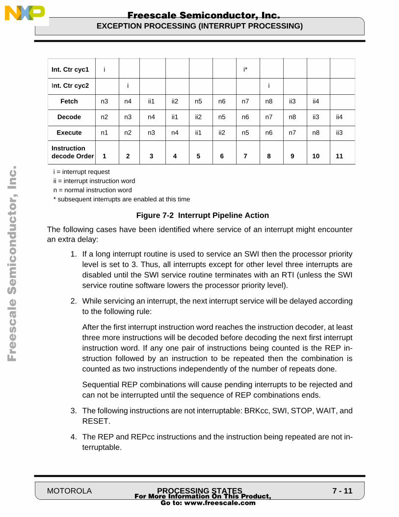
EXCEPTION PROCESSING (INTERRUPT PROCESSING)
Fre
esc
ale
Se
mic
on
du
cto
r, I
Freescale Semiconductor, Inc.n
c..
.
The following cases have been identified where service of an interrupt might encounteran extra delay:
1. If a long interrupt routine is used to service an SWI then the processor prioritylevel is set to 3. Thus, all interrupts except for other level three interrupts aredisabled until the SWI service routine terminates with an RTI (unless the SWIservice routine software lowers the processor priority level).
2. While servicing an interrupt, the next interrupt service will be delayed accordingto the following rule:
After the first interrupt instruction word reaches the instruction decoder, at leastthree more instructions will be decoded before decoding the next first interruptinstruction word. If any one pair of instructions being counted is the REP in-struction followed by an instruction to be repeated then the combination iscounted as two instructions independently of the number of repeats done.
Sequential REP combinations will cause pending interrupts to be rejected andcan not be interrupted until the sequence of REP combinations ends.
3. The following instructions are not interruptable: BRKcc, SWI, STOP, WAIT, andRESET.
4. The REP and REPcc instructions and the instruction being repeated are not in-terruptable.
Int. Ctr cyc1 i i*
Int. Ctr cyc2 i i
Fetch n3 n4 ii1 ii2 n5 n6 n7 n8 ii3 ii4
Decode n2 n3 n4 ii1 ii2 n5 n6 n7 n8 ii3 ii4
Execute n1 n2 n3 n4 ii1 ii2 n5 n6 n7 n8 ii3
Instructiondecode Order 1 2 3 4 5 6 7 8 9 10 11
i = interrupt request ii = interrupt instruction word n = normal instruction word * subsequent interrupts are enabled at this time
Figure 7-2 Interrupt Pipeline Action
MOTOROLA PROCESSING STATES 7 - 11 For More Information On This Product,
Go to: www.freescale.com
EXCEPTION PROCESSING (INTERRUPT PROCESSING)
Fre
esc
ale
Se
mic
on
du
cto
r, I
Freescale Semiconductor, Inc.n
c..
.
5. Instructions using a Read-Modify-Write bus access cannot be interrupted dur-ing their bus access.
During an interrupt instruction fetch, two instruction words are fetched, the first from theinterrupt starting address and the second from the interrupt starting address +1 loca-tions.
7.3.1 Interrupt TypesTwo types of interrupt routines may be used: fast and long. The fast routine consists ofthe two automatically inserted interrupt instruction words. These words can contain anyun-restricted single two-word instruction or any two one-word instructions (see AppendixA - section A.8 “Instruction Sequence Restrictions” for a list of restrictions). Fast interruptroutines are never interruptable.
CAUTIONStatus is not preserved during a fast interrupt routine; therefore, instructionswhich modify status should not be used at the interrupt starting address andinterrupt starting address +1.
If one of the instructions in the fast routine is a jump or branch to subroutine, then a longinterrupt routine is formed. The long interrupt routine should be terminated by an RTI.Long interrupt routines are interruptable by higher priority interrupts.
7.3.2 Interrupt ArbitrationExternal interrupts are internally synchronized with the processor clock (this takes up tothree T cycles) before their interrupt pending flags are set. Each separate external inter-rupt and internal interrupt has its own independent flag. After each instruction is exe-cuted in normal processing mode, all interrupts are arbitrated. This includes all hardwareinterrupts that have been latched into their respective interrupt pending flags and allinternal interrupts. During arbitration, each interrupt’s IPL is compared with the interruptmask in the SR and the interrupt is either allowed or disallowed. The remaining interruptsare prioritized according to the priority shown in Table 7-5 and the highest priority inter-rupt is chosen. The interrupt vector is then calculated so that the Program Interrupt Con-troller can fetch the first interrupt instruction. Interrupt arbitration and control occursconcurrently with the fetch-decode-execute cycle and takes two instruction cycles. Inter-rupts from a given source are not buffered. The interrupt pending flag for the choseninterrupt is not cleared until the second interrupt vector of the chosen interrupt is beingfetched. A new interrupt from the same source will not be accepted for the next interruptarbitration until that time.
7 - 12 PROCESSING STATES MOTOROLA For More Information On This Product,
Go to: www.freescale.com
EXCEPTION PROCESSING (INTERRUPT PROCESSING)
Fre
esc
ale
Se
mic
on
du
cto
r, I
Freescale Semiconductor, Inc.n
c..
.
The internal “interrupt acknowledge” signal is used to clear the edge-triggered interrupts’flags, the Stack Error, Illegal Interrupt and SWI. Peripheral interrupt requests that need aread/write action to some register DO NOT receive this signal, and those interrupts willremain pending until their registers are read/written. Also, level-triggered interrupts willnot be cleared. Note that the acknowledge signal will be generated after generation ofthe interrupt vectors, and not before.
However, the first instruction word of the next interrupt service will reach the decoderonly after the decoding of at least four instructions following the decoding of the firstinstruction of the previous interrupt.
7.3.3 Interrupt Instruction FetchThe interrupt controller generates an interrupt instruction fetch address which points tothe first instruction word of a two-word fast interrupt routine. This address is used for thenext instruction fetch, instead of the PC, and the interrupt instruction fetch address + 1 isused for the subsequent instruction fetch. While the interrupt instructions are beingfetched, the PC is inhibited from being updated. After the two interrupt words have beenfetched, the PC is used for any following instruction fetches.
After the interrupt instructions have been fetched, they are guaranteed to be executed.This is true even if the instruction that is currently being executed is a change of flowinstruction (i.e., JMP, JSR, etc.) that would normally ignore the instructions in the pipe.After the interrupt instruction fetch, the PC will point to the instruction that would havebeen fetched if the interrupt instructions had not been substituted.
7.3.4 Interrupt Instruction Execution Interrupt instruction execution is considered to be “fast” if neither of the instructions of theinterrupt service routine causes a change of flow. A jump or branch to subroutine within afast interrupt routine forms a long interrupt which is terminated with an RTI instruction torestore the PC and SR from the stack and return to normal program execution. Reset isa special exception which will normally contain only a JMP instruction at the exceptionstart address. At the programmer’s option, almost any instruction can be used in the fastinterrupt routine. The restricted instructions include SWI, STOP, and WAIT. Figure 7-3,Figure 7-4, Figure 7-5 show the fast and the long interrupt service routines. Notice thatthe fast interrupt executes only two instructions and then automatically resumes execu-tion of the main program where it left off whereas the long interrupt must be told to returnto the main program by executing an RTI instruction.
7.3.4.1 Fast InterruptFigure 7-3 illustrates the effect of a fast interrupt routine in the stream of instructionfetches.
MOTOROLA PROCESSING STATES 7 - 13 For More Information On This Product,
Go to: www.freescale.com
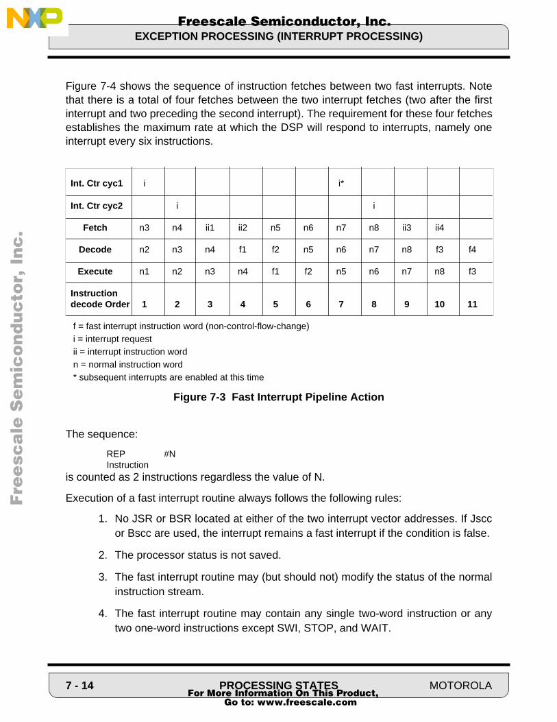
EXCEPTION PROCESSING (INTERRUPT PROCESSING)
Fre
esc
ale
Se
mic
on
du
cto
r, I
Freescale Semiconductor, Inc.n
c..
.
Figure 7-4 shows the sequence of instruction fetches between two fast interrupts. Notethat there is a total of four fetches between the two interrupt fetches (two after the firstinterrupt and two preceding the second interrupt). The requirement for these four fetchesestablishes the maximum rate at which the DSP will respond to interrupts, namely oneinterrupt every six instructions.
The sequence:
REP #NInstruction
is counted as 2 instructions regardless the value of N.
Execution of a fast interrupt routine always follows the following rules:
1. No JSR or BSR located at either of the two interrupt vector addresses. If Jsccor Bscc are used, the interrupt remains a fast interrupt if the condition is false.
2. The processor status is not saved.
3. The fast interrupt routine may (but should not) modify the status of the normalinstruction stream.
4. The fast interrupt routine may contain any single two-word instruction or anytwo one-word instructions except SWI, STOP, and WAIT.
Int. Ctr cyc1 i i*
Int. Ctr cyc2 i i
Fetch n3 n4 ii1 ii2 n5 n6 n7 n8 ii3 ii4
Decode n2 n3 n4 f1 f2 n5 n6 n7 n8 f3 f4
Execute n1 n2 n3 n4 f1 f2 n5 n6 n7 n8 f3
Instructiondecode Order 1 2 3 4 5 6 7 8 9 10 11
f = fast interrupt instruction word (non-control-flow-change) i = interrupt request ii = interrupt instruction word n = normal instruction word * subsequent interrupts are enabled at this time
Figure 7-3 Fast Interrupt Pipeline Action
7 - 14 PROCESSING STATES MOTOROLA For More Information On This Product,
Go to: www.freescale.com
EXCEPTION PROCESSING (INTERRUPT PROCESSING)
Fre
esc
ale
Se
mic
on
du
cto
r, I
Freescale Semiconductor, Inc.n
c..
.
5. The PC, which contains the address of the next instruction to be executed innormal processing, remains unchanged during a fast interrupt routine.
6. The fast interrupt returns without an RTI.
7. Normal instruction fetching resumes using the PC following the completion ofthe fast interrupt routine.
8. A fast interrupt is not interruptable.
9. The primary application is to move data between memory and I/O devices.
7.3.4.2 Long InterruptA jump to subroutine instruction within the fast interrupt routine forms a long interruptroutine. Execution of a long interrupt routine always follows the following rules:
1. A JSR, BSR, JScc or BScc with true condition to the starting address of the in-terrupt service routine is located at one of the two interrupt vector addresses.
2. During execution of the jump to subroutine instruction, the PC and SR arestacked. The interrupt mask bits of the SR are updated to mask interrupts of thesame or lower priority. The Loop Flag and Scaling Mode bits are reset.
3. The first instruction word of the next interrupt service (of higher IPL) will reachthe decoder only after the decoding of at least four instructions following the de-coding of the first instruction of the previous interrupt.
4. The interrupt service routine can be interrupted i.e., nested interrupts are sup-ported.
5. The long interrupt routine can be any length and should be terminated by anRTI, which restores the PC and SR from the stack.
Figure 7-4 illustrates the effect of a long interrupt routine on the instruction pipeline. Ashort JSR (that is, a JSR with 8-bit absolute address) is used to form the long interruptroutine. For this example, word 4 of the long interrupt routine is an RTI. A subsequentinterrupt is shown to illustrate the non-interruptible nature of the early instructions in thelong interrupt service routine. In this example, the interrupts are reenabled, not becausesr4 was an RTI, but because it was the fourth instruction decoded after ii1 was decodedand found to be a JSR instruction.
Either one of the two instructions of the fast interrupt can be the JSR instruction thatforms the long interrupt. Notice that if the first fast interrupt vector instruction is a shortJSR, the second instruction is never used.
MOTOROLA PROCESSING STATES 7 - 15 For More Information On This Product,
Go to: www.freescale.com
EXCEPTION PROCESSING (INTERRUPT PROCESSING)
Fre
esc
ale
Se
mic
on
du
cto
r, I
Freescale Semiconductor, Inc.n
c..
.
7.3.4.3 Case of the REP InstructionA REP instruction is treated as a single two-word instruction regardless of how manytimes it repeats the second instruction of the pair. Instruction fetches are suspended andwill be reactivated only after the loop counter is decremented to one
See Figure 7-5 for an example of interrupt service when the instruction that receives theinternal interrupt service request is the REP instruction (n3 in Figure 7-5). During therepeated executions of the instruction that follows the REP instruction (n4), instructionfetches are suspended. The fetches will be reactivated only after the loop counter is dec-remented to one. During the execution of n4, no interrupts will be serviced. When LCfinally reaches one, the fetches are reinitiated and the interrupt can be serviced. In Fig-ure 7-5 it can be seen that n5 (loaded into the instruction latch from the backup instruc-tion latch) is decoded and executed as well as n6 before the first interrupt vector.
Sequential REP operations will cause pending interrupts to be rejected and can not beinterrupted until the sequence of REP operations ends. The reason that REP operationsare not interruptable is that the instruction being repeated is not refetched. While thatinstruction is repeating, no instructions are fetched or decoded and an interrupt can notbe inserted.
7.3.5 Interrupt Sources Exceptions may originate from any of the 32 vector addresses listed in Table 7-1 Thecorresponding interrupt starting addresses for each interrupt source are shown. Interruptstarting addresses are internally-generated addresses which point to the first instructionof the fast interrupt service routine. The interrupt starting address for each interrupt is anaddress constant for minimum overhead. Thirty-two interrupt starting address locationsare provided. These addresses are located in the first 64 locations of program memory.When an interrupt is serviced, the instruction at the interrupt starting address is fetchedfirst. If it is known a priori that certain interrupts will not be used, those interrupt vectorlocations can be used for program or data storage.
The 32 interrupts are prioritized into four levels. Level 3 is the highest priority level and isnot maskable. Levels 0-2 are maskable. The interrupts within each level are prioritizedaccording to a predefined priority that is discussed in the next sub-section. The levelthree interrupts - Reset, Illegal Instruction, Stack Error and SWI, are discussed individu-ally.
7.3.5.1 Hardware Interrupt Sources There are two types of hardware interrupts in the DSP: internal and external. The internalinterrupts include all of the on-chip peripheral devices (Host Interface, SSIs and Timer).Each internal interrupt source is latched and serviced if it is not masked. When it is ser-
7 - 16 PROCESSING STATES MOTOROLA For More Information On This Product,
Go to: www.freescale.com

EXCEPTION PROCESSING (INTERRUPT PROCESSING)
Fre
esc
ale
Se
mic
on
du
cto
r, I
Freescale Semiconductor, Inc.n
c..
.
Int. Ctr cyc1 i i*
Int. Ctr cyc2 i i
Fetch n3 n4 ii1 ii2 sr1 sr2 sr3 sr4 sr5 n5 ii1
Decode n2 n3 n4 JSRf – sr1 sr2 sr3 RTI – n5
Execute n1 n2 n3 n4 JSRf NOP sr1 sr2 sr3 RTI NOP
Instructiondecode Order 1 2 3 4 5 6 7 8 9
Int. Ctr cyc1 i*
Int. Ctr cyc2 i
Fetch sr5 n5 ii1 ii2 n6 n7 n8 n9
Decode RTI – n5 ii1 ii2 n6 n7 n8
Execute sr3 RTI NOP n5 ii1 ii2 n6 n7
Instructiondecode Order 8 9 19 11 12 13 14
i = interrupt request ii = interrupt instruction word JSRf = fast JSR (JSR with 8-bit absolute address) n = normal instruction word sr = service routine word * subsequent interrupts are enabled at this time
instruction after the RTI is always fetched but notdecoded when RTI has been recognized
Figure 7-4 Long Interrupt Pipeline Action
MOTOROLA PROCESSING STATES 7 - 17 For More Information On This Product,
Go to: www.freescale.com

EXCEPTION PROCESSING (INTERRUPT PROCESSING)
F
ree
sca
le S
em
ico
nd
uc
tor,
I
Freescale Semiconductor, Inc.n
c..
.
viced, the interrupt is cleared. Each internal hardware source has independent enablecontrol and priority level control.
The external hardware interrupts include RESET, IRQA, and IRQB. The RESET interruptis level sensitive and is the highest level interrupt (priority 3). The IRQA and IRQB inter-rupts can be programmed to be level sensitive or edge sensitive. The level sensitiveinterrupts will not be cleared automatically when they are serviced and therefore must becleared by other means to prevent multiple interrupts. The edge sensitive interrupts arelatched as pending on the high-to-low transition of the interrupt input and automaticallycleared when the interrupt is serviced. IRQA and IRQB interrupts can be programmed toone of three maskable priority levels: level 0, 1, or 2. Additionally, both of these interruptshave independent enable control.
When the IRQA or IRQB interrupts are disabled in the IPR register, the pending requestwill be ignored regardless of whether the interrupt input was defined as level sensitive oredge sensitive. If the interrupt is defined as edge sensitive, its edge detection latch willremain in the reset state as long as (1) the interrupt is disabled or (2) if the interrupt isdefined as level sensitive. If the level sensitive interrupt is disabled while the interrupt ispending, the pending interrupt will be cancelled. However, if the first instruction of theinterrupt has been fetched, it will not be cancelled.
Int. Ctr cyc1 i i
Int. Ctr cyc2 i% i*
Fetch n3 n4 n5 n6 ii1 ii2 n7 n8 n9
Decode n2 REP – n4 n4 n5 n6 ii1 ii2 n7 n8
Execute n1 n2 REP NOP n4 n4 n5 n6 ii1 ii2 n7
Instructiondecode Order 1 2 3 4 5 6 7 8 9 10 11
i = interrupt request ii = interrupt instruction word n = normal instruction word n3 = REP #2 instruction n4 = instruction being repeated twice n5 = instruction that waits in the backup instruction latch% interrupt rejected at this time * subsequent interrupts are enabled at this time
Figure 7-5 Example of Interrupt Service when
Interrupt is Presented to REP Instruction
7 - 18 PROCESSING STATES MOTOROLA For More Information On This Product,
Go to: www.freescale.com
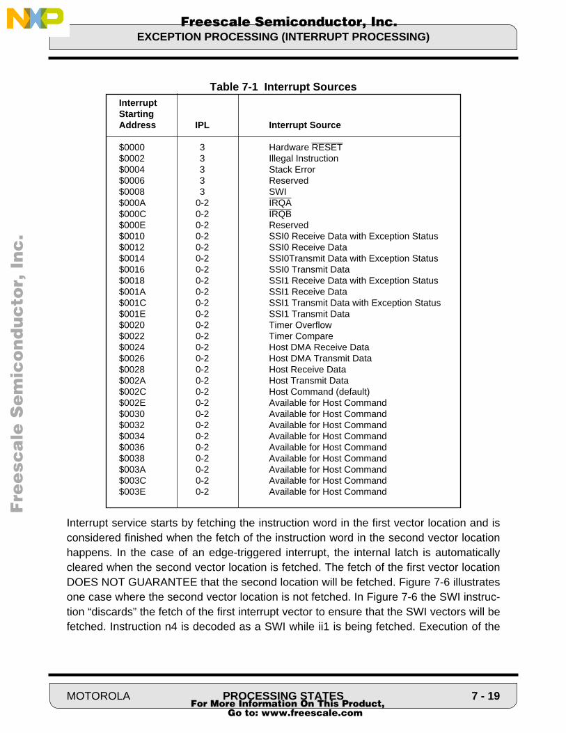
EXCEPTION PROCESSING (INTERRUPT PROCESSING)
F
ree
sca
le S
em
ico
nd
uc
tor,
I
Freescale Semiconductor, Inc.n
c..
.
Table 7-1 Interrupt Sources
Interrupt service starts by fetching the instruction word in the first vector location and isconsidered finished when the fetch of the instruction word in the second vector locationhappens. In the case of an edge-triggered interrupt, the internal latch is automaticallycleared when the second vector location is fetched. The fetch of the first vector locationDOES NOT GUARANTEE that the second location will be fetched. Figure 7-6 illustratesone case where the second vector location is not fetched. In Figure 7-6 the SWI instruc-tion “discards” the fetch of the first interrupt vector to ensure that the SWI vectors will befetched. Instruction n4 is decoded as a SWI while ii1 is being fetched. Execution of the
InterruptStartingAddress IPL Interrupt Source $0000 3 Hardware RESET$0002 3 Illegal Instruction $0004 3 Stack Error$0006 3 Reserved$0008 3 SWI$000A 0-2 IRQA$000C 0-2 IRQB$000E 0-2 Reserved$0010 0-2 SSI0 Receive Data with Exception Status$0012 0-2 SSI0 Receive Data $0014 0-2 SSI0Transmit Data with Exception Status$0016 0-2 SSI0 Transmit Data $0018 0-2 SSI1 Receive Data with Exception Status$001A 0-2 SSI1 Receive Data $001C 0-2 SSI1 Transmit Data with Exception Status$001E 0-2 SSI1 Transmit Data $0020 0-2 Timer Overflow$0022 0-2 Timer Compare$0024 0-2 Host DMA Receive Data$0026 0-2 Host DMA Transmit Data$0028 0-2 Host Receive Data$002A 0-2 Host Transmit Data$002C 0-2 Host Command (default)$002E 0-2 Available for Host Command$0030 0-2 Available for Host Command$0032 0-2 Available for Host Command$0034 0-2 Available for Host Command$0036 0-2 Available for Host Command$0038 0-2 Available for Host Command$003A 0-2 Available for Host Command$003C 0-2 Available for Host Command$003E 0-2 Available for Host Command
MOTOROLA PROCESSING STATES 7 - 19 For More Information On This Product,
Go to: www.freescale.com

EXCEPTION PROCESSING (INTERRUPT PROCESSING)
F
ree
sca
le S
em
ico
nd
uc
tor,
I
Freescale Semiconductor, Inc.n
c..
.
SWI requires that ii1 be discarded and the two SWI instructions (ii3 and ii4) be fetchedinstead.
CAUTIONOn all level sensitive interrupts, the interrupt must be externally released be-fore interrupts are internally re-enabled or the processor will be interruptedrepeatedly until the interrupt is released.
7.3.5.2 Software Interrupt SourcesThere are two software interrupt sources - Illegal Instruction Interrupt (III) and SoftwareInterrupt (SWI).
7.3.5.2.1 Illegal Instruction Interrupt
III is a non-maskable interrupt (IPL 3) which is serviced immediately following the execu-tion of the ILLEGAL instruction or the attempted execution of an illegal instruction (anyundefined operation code). Illegal instruction interrupts are fatal errors. Only a long inter-rupt routine should be used for the III routine. As shown in Figure 7-7, if a fast interrupt ischosen, everything being frozen after the decode of n5 (II), this same instruction will bedecoded again after execution of the two fast interrupt words. Execution will thereforeloop forever between the illegal instruction and its fast interrupt routine. Even when along interrupt is used, no RTI or RTS should be used at the end of the interrupt routine,since return from the illegal instruction interrupt to the main code will result in decoding
Int. Ctr cyc1 i i*
Int. Ctr cyc2 i i*
Fetch n3 n4 n5 ii1 ii3 ii4 sw1 sw2 sw3 sw4
Decode n2 n3 SWI -- -- -- JSR -- sw1 sw2 sw3
Execute n1 n2 n3 SWI NOP NOP NOP JSR -- sw1 sw2
Instructiondecode Order 1 2 3 4 5 6 7
i = interrupt request i* = interrupt request generated by SWI ii1 = 1st vector of interrupt i ii3 = 1st SWI vector (1-word JSR) ii4 = 2nd SWI vector n = normal instruction word n4 = SWI sw = instructions pertaining to the SWI long interrupt routine
Figure 7-6 Software Interrupt Mechanism
7 - 20 PROCESSING STATES MOTOROLA For More Information On This Product,
Go to: www.freescale.com
EXCEPTION PROCESSING (INTERRUPT PROCESSING)
F
ree
sca
le S
em
ico
nd
uc
tor,
I
Freescale Semiconductor, Inc.n
c..
.
the illegal instruction again. During the illegal instruction interrupt service, the JSRlocated in the III vector will normally stack the address of the illegal instruction. The usermay examine the stack (using MOVE SSH,dest) to locate the offending illegal instruc-tion. The ILLEGAL instruction is useful for triggering the illegal interrupt service to see ifthe III routine is capable of recovery from illegal instructions.
There are two cases in which the stacked address will not point to the illegal instruction:
1. If the illegal instruction is one of the two instructions at an interrupt vector loca-tion, and is fetched during a regular interrupt service, the processor will stackthe address of the next sequential instruction in the normal instruction flow (theregular return address of the interrupt routine that had the illegal opcode in itsvector).
2. If the illegal instruction follows a REP instruction (see Figure 7-8), the DSP willeffectively execute the illegal instruction as a repeated NOP, the interrupt vec-tor will then be inserted in the pipeline. The next instruction will be fetched butnot decoded or executed. The processor will stack the address of the next se-quential instruction (i.e., n8 in Figure 7-8) which is two instructions after the il-legal instruction.
In DO loops, if the illegal instruction is in the LA location, and the instruction preceding it(i.e. at LA-1) is being interrupted with a normal interrupt, the LC will be decremented as ifthe loop had reached the LA instruction. When the interrupt service ends and the instruc-tion flow returns to the loop, the illegal instruction will be refetched (since it is the nextsequential instruction in the flow). The loop state machine will again decrement LCbecause the LA instruction is being executed. At this point, the illegal instruction will trig-ger the illegal instruction interrupt. Notice that the loop state machine decremented LCtwice in one loop due to the presence of the illegal opcode at the LA location. This is aspecial condition that only happens during this situation.
7.3.5.2.2 Software Interrupt
SWI is a non-maskable interrupt (IPL 3) which is serviced immediately following the soft-ware interrupt instruction execution. A long interrupt service routine is usually used. Thedifference between a SWI and a JSR instruction is that the SWI sets the interrupt maskto prevent interrupts with an IPL below three from being serviced. Masking out lowerlevel interrupts makes the SWI very useful for setting breakpoints in monitor programs.The JSR instruction does not affect the interrupt mask.
7.3.5.3 Stack Error InterruptThe stack error interrupt is non-maskable (IPL 3). An overflow or underflow of the stackcauses a stack error interrupt (see Section 5 for additional information on the stack error
MOTOROLA PROCESSING STATES 7 - 21 For More Information On This Product,
Go to: www.freescale.com
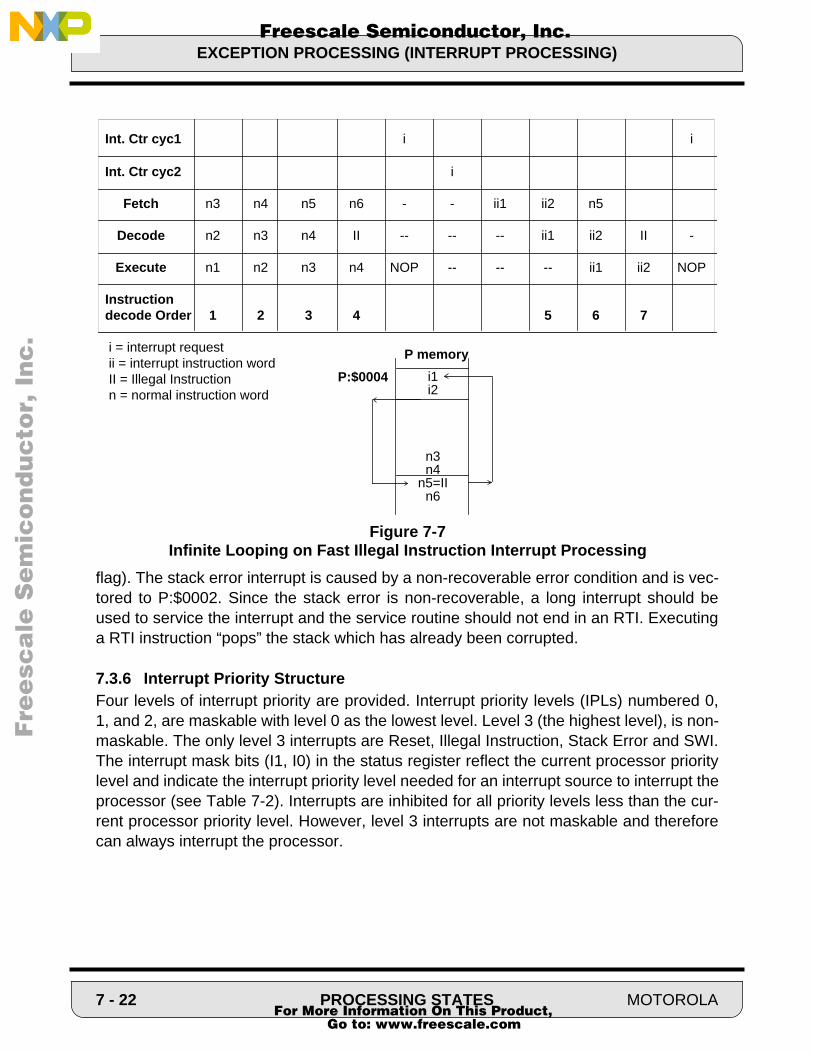
EXCEPTION PROCESSING (INTERRUPT PROCESSING)
F
ree
sca
le S
em
ico
nd
uc
tor,
I
Freescale Semiconductor, Inc.n
c..
.
flag). The stack error interrupt is caused by a non-recoverable error condition and is vec-tored to P:$0002. Since the stack error is non-recoverable, a long interrupt should beused to service the interrupt and the service routine should not end in an RTI. Executinga RTI instruction “pops” the stack which has already been corrupted.
7.3.6 Interrupt Priority Structure Four levels of interrupt priority are provided. Interrupt priority levels (IPLs) numbered 0,1, and 2, are maskable with level 0 as the lowest level. Level 3 (the highest level), is non-maskable. The only level 3 interrupts are Reset, Illegal Instruction, Stack Error and SWI.The interrupt mask bits (I1, I0) in the status register reflect the current processor prioritylevel and indicate the interrupt priority level needed for an interrupt source to interrupt theprocessor (see Table 7-2). Interrupts are inhibited for all priority levels less than the cur-rent processor priority level. However, level 3 interrupts are not maskable and thereforecan always interrupt the processor.
Int. Ctr cyc1 i i
Int. Ctr cyc2 i
Fetch n3 n4 n5 n6 - - ii1 ii2 n5
Decode n2 n3 n4 II -- -- -- ii1 ii2 II -
Execute n1 n2 n3 n4 NOP -- -- -- ii1 ii2 NOP
Instructiondecode Order 1 2 3 4 5 6 7
i = interrupt request ii = interrupt instruction word II = Illegal Instruction n = normal instruction word
Figure 7-7 Infinite Looping on Fast Illegal Instruction Interrupt Processing
i1i2
n3n4
n5=IIn6
P memory
P:$0004
7 - 22 PROCESSING STATES MOTOROLA For More Information On This Product,
Go to: www.freescale.com

EXCEPTION PROCESSING (INTERRUPT PROCESSING)
F
ree
sca
le S
em
ico
nd
uc
tor,
I
Freescale Semiconductor, Inc.n
c..
.
Table 7-2 Status Register Interrupt Mask Bits
7.3.6.1 Interrupt Priority Levels (IPL) The interrupt priority level for each on-chip peripheral device and for each external inter-rupt source (IRQA, IRQB) can be programmed under software control. Each on-chip orexternal peripheral device can be programmed to one of the three maskable priority lev-els (IPL 0, 1, or 2). Interrupt priority levels are set by writing to the Interrupt Priority Reg-ister shown in Figure 7-9. This read/write register specifies the interrupt priority level foreach of the interrupting devices (HOST, SSIs, Timer, IRQA, IRQB). In addition, this reg-ister specifies the trigger mode of both external interrupt sources and it is used to enableor disable the individual external interrupts. This register is cleared on RESET. Table 7-3defines the interrupt priority level bits. Table 7-4 defines the external interrupt triggermode bits.
Int. Ctr cyc1 i i
Int. Ctr cyc2 i
Fetch n3 n4 n5 n6 n7 - - ii1 ii2 n8
Decode n2 n3 n4 REP II -- -- -- ii1 ii2 n8
Execute n1 n2 n3 n4 REP NOP -- -- -- ii1 ii2
Instructiondecode Order 1 2 3 4 5 6 7 8
i = interrupt request ii = interrupt instruction word II = Illegal Instruction n = normal instruction word
Figure 7-8 Repeated Illegal Instruction
I1 I0 Exceptions Exceptions Permitted Masked
0 0 IPL 0,1,2,3 None0 1 IPL 1,2,3 IPL 01 0 IPL 2,3 IPL 0,11 1 IPL 3 IPL 0,1,2,
MOTOROLA PROCESSING STATES 7 - 23 For More Information On This Product,
Go to: www.freescale.com
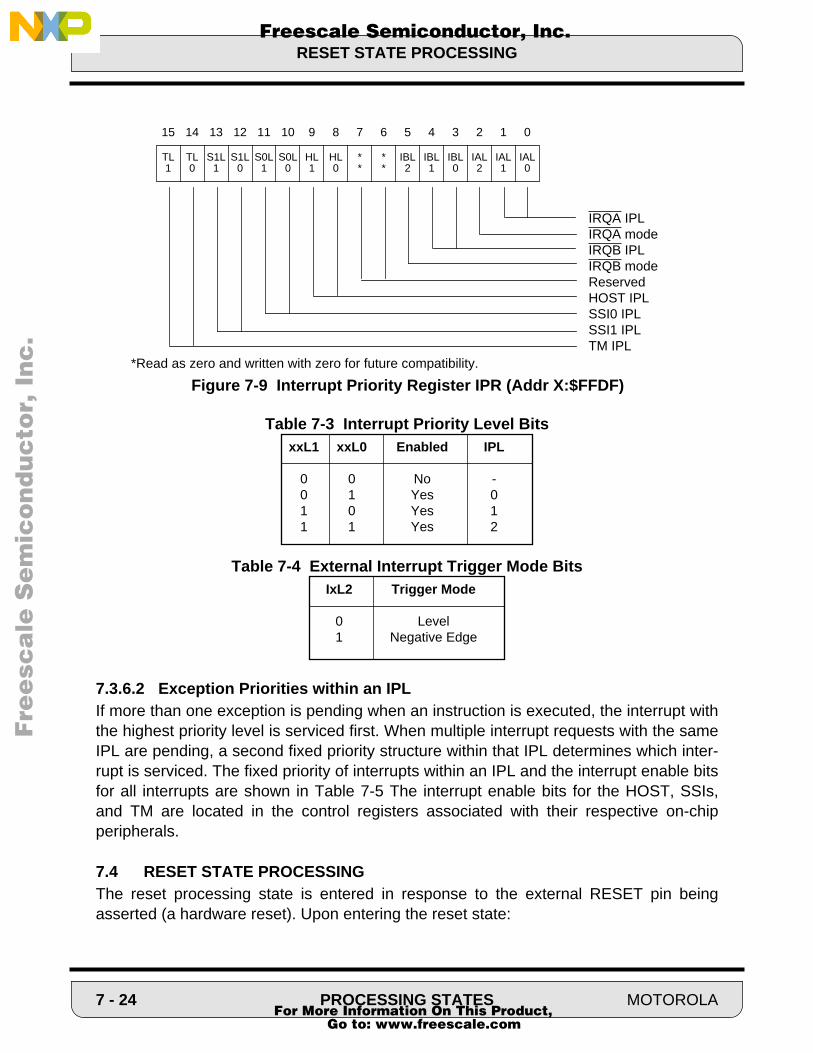
RESET STATE PROCESSING
F
ree
sca
le S
em
ico
nd
uc
tor,
I
Freescale Semiconductor, Inc.n
c..
.
Table 7-3 Interrupt Priority Level Bits
Table 7-4 External Interrupt Trigger Mode Bits
7.3.6.2 Exception Priorities within an IPL If more than one exception is pending when an instruction is executed, the interrupt withthe highest priority level is serviced first. When multiple interrupt requests with the sameIPL are pending, a second fixed priority structure within that IPL determines which inter-rupt is serviced. The fixed priority of interrupts within an IPL and the interrupt enable bitsfor all interrupts are shown in Table 7-5 The interrupt enable bits for the HOST, SSIs,and TM are located in the control registers associated with their respective on-chipperipherals.
7.4 RESET STATE PROCESSINGThe reset processing state is entered in response to the external RESET pin beingasserted (a hardware reset). Upon entering the reset state:
15 14 13 12 11 10 9 8 7 6 5 4 3 2 1 0
TL TL S1L S1L S0L S0L HL HL * * IBL IBL IBL IAL IAL IAL1 0 1 0 1 0 1 0 * * 2 1 0 2 1 0
IRQA IPLIRQA modeIRQB IPLIRQB modeReservedHOST IPLSSI0 IPLSSI1 IPLTM IPL
*Read as zero and written with zero for future compatibility.
Figure 7-9 Interrupt Priority Register IPR (Addr X:$FFDF)
xxL1 xxL0 Enabled IPL
0 0 No -0 1 Yes 01 0 Yes 11 1 Yes 2
IxL2 Trigger Mode
0 Level1 Negative Edge
7 - 24 PROCESSING STATES MOTOROLA For More Information On This Product,
Go to: www.freescale.com
WAIT STATE PROCESSING
F
ree
sca
le S
em
ico
nd
uc
tor,
I
Freescale Semiconductor, Inc.n
c..
.
1. internal peripheral devices are reset, and their pins revert to general-purpose I/O pins.
2. the modifier registers are set to $FFFF.
3. the interrupt priority register is cleared.
4. the BCR is set to $43FF, thereby inserting 31 wait states in all external memoryaccesses.
5. the stack pointer is cleared.
6. the loop flag, forever flag, scaling mode are cleared in the MR register, the in-terrupt mask bits are set, and all CCR bits are cleared.
7. the OMR bits CD (Clockout Disable), SD (Stop delay), R (Rounding), SA (Sat-uration) are cleared.
The DSP remains in the reset state until RESET is deasserted. Upon leaving the resetstate:
1. the chip operating mode bits of the OMR are loaded from the external mode se-lect pins (MODA, MODB, MOBC).
2. program execution begins at program memory address $E000 in normal ex-panded mode or at $0000 in all other operation modes. The first instructionmust be fetched and then decoded before executing. Therefore, the first in-struction is executed two instruction cycles after the first instruction fetch. TwoNOPs are executed in the two instruction cycles before the first instruction isexecuted.
The internal peripheral devices (HI, SSI0, SSI1, and ports A, B, and C) can be reset byseveral methods – hardware (HW) reset, software (SW) reset, individual (I) reset, andstop (ST) reset. Depending on the type of reset, the registers of these devices will beaffected differently (see SECTIONS 8,9,10,11,12 for additional information on the inter-nal peripherals).
7.5 WAIT STATE PROCESSINGThe wait processing state is a low power consumption state entered by execution of theWAIT instruction. In the wait state, the internal clock is disabled to all internal circuitryexcept the internal peripherals. All internal processing is halted until an unmasked inter-rupt occurs or the DSP is reset. The bus arbitration circuits (BR, BG, and BB pins)remain active during the Wait state if the DSP was in the slave mode (MC=0) beforeentering the WAIT state. The wait state is one of two low power states.
MOTOROLA PROCESSING STATES 7 - 25 For More Information On This Product,
Go to: www.freescale.com
WAIT STATE PROCESSING
F
ree
sca
le S
em
ico
nd
uc
tor,
I
Freescale Semiconductor, Inc.n
c..
.
Figure 7-10 shows a WAIT instruction being fetched, decoded, and executed. It isfetched as n3 in this example and during decode is recognized as a WAIT instruction.The following instruction (n4) is aborted and the internal clock is disabled from all internalcircuitry except the internal peripherals. The processor stays in this state until an inter-rupt or reset is recognized. The response time is variable due to the timing of the inter-rupt with respect to the internal clock. Figure 7-10 shows the result of a fast interruptbringing the processor out of the wait state. The two appropriate interrupt vectors arefetched and put in the instruction pipe. The next instruction fetched is n4 which had beenaborted earlier. Instruction execution proceeds normally from this point on.
Figure 7-11 shows an example of the WAIT instruction being executed at the same timethat an interrupt is pending. Instruction n4 is aborted as before. There is a five instructioncycle delay caused by the WAIT instruction and then the interrupt is processed normally.The internal clocks are not turned off and the net effect is that of executing eight NOPinstructions between the execution of n2 and ii1.
7 - 26 PROCESSING STATES MOTOROLA For More Information On This Product,
Go to: www.freescale.com
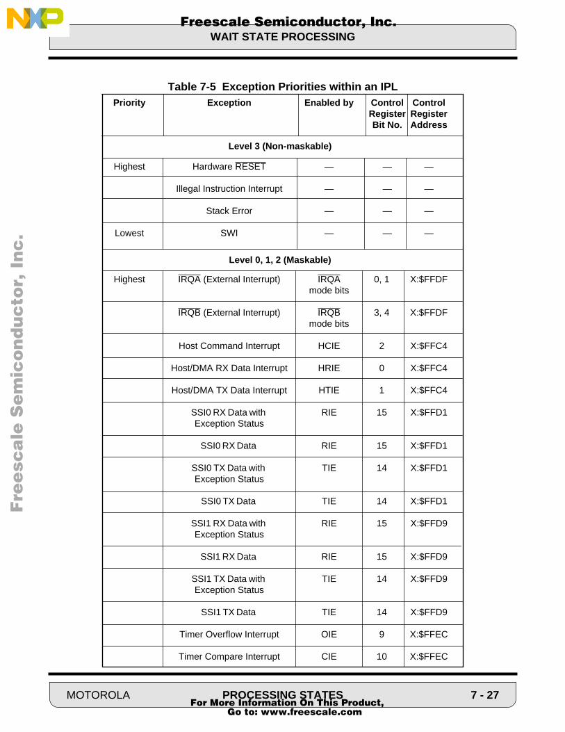
WAIT STATE PROCESSING
F
ree
sca
le S
em
ico
nd
uc
tor,
I
Freescale Semiconductor, Inc.n
c..
.
Table 7-5 Exception Priorities within an IPLPriority Exception Enabled by Control Control
Register RegisterBit No. Address
Highest Hardware RESET — — —
Illegal Instruction Interrupt — — —
Stack Error — — —
Lowest SWI — — —
Level 3 (Non-maskable)
Level 0, 1, 2 (Maskable)
Highest IRQA (External Interrupt) IRQA 0, 1 X:$FFDFmode bits
IRQB (External Interrupt) IRQB 3, 4 X:$FFDFmode bits
Host Command Interrupt HCIE 2 X:$FFC4
Host/DMA RX Data Interrupt HRIE 0 X:$FFC4
Host/DMA TX Data Interrupt HTIE 1 X:$FFC4
SSI0 RX Data with RIE 15 X:$FFD1Exception Status
SSI0 RX Data RIE 15 X:$FFD1
SSI0 TX Data with TIE 14 X:$FFD1Exception Status
SSI0 TX Data TIE 14 X:$FFD1
SSI1 RX Data with RIE 15 X:$FFD9Exception Status
SSI1 RX Data RIE 15 X:$FFD9
SSI1 TX Data with TIE 14 X:$FFD9Exception Status
SSI1 TX Data TIE 14 X:$FFD9
Timer Overflow Interrupt OIE 9 X:$FFEC
Timer Compare Interrupt CIE 10 X:$FFEC
MOTOROLA PROCESSING STATES 7 - 27 For More Information On This Product,
Go to: www.freescale.com

STOP STATE PROCESSING
F
ree
sca
le S
em
ico
nd
uc
tor,
I
Freescale Semiconductor, Inc.n
c..
.
During the wait state, the BR/BG/BB circuits remain active if the DSP was in the slavemode. Before BR is asserted (see Table 7-6), all Port A signals are driven. The controlsignals are deasserted, the data signals are inputs and the address signals remain asthe last address read or written. When BG is asserted, all signal are three-stated (highimpedance). Immediately after BR is deasserted, the R/W, PS/DS, and TS signals aredriven high — all other signals remain three-stated. During the first T0 clock state follow-ing the exit from the wait state, control signals PS/DS, TS are again driven — the dataand address signals remain three-stated. During first external access, all signals returnto their normal operating mode.
Table 7-6 BR/BG During WAIT (Slave Mode)
7.6 STOP STATE PROCESSINGThe stop processing state is the lowest power consumption state and is entered by theexecution of the STOP instruction. In the stop state, all circuits are powered down except
Int. Ctr cyc1 i
Int. Ctr cyc2 i*
Fetch n3 n4 - ii1 ii2 n4 n5 n6
Decode n2 WAIT - ii1 ii2 n4 n5
Execute n1 n2 WAIT - ii1 ii2 n4
Instructiondecode Order 1 2 3 4 5 6
i = interrupt request ii = interrupt instruction word n = normal instruction word
Figure 7-10 WAIT Instruction
Before BR While BG After BR After Return to After 1stSignal Asserted Asserted Deasserted Normal State External Access
PS/DS Output Hi-Z Hi-Z Output Output
TS Output Hi-Z Hi-Z Output Output
R/W Output Hi-Z Output Output Output
Data I/O Hi-Z Hi-Z Hi-Z I/O
Address Output Hi-Z Hi-Z Hi-Z Output
(Read)
from Wait State
7 - 28 PROCESSING STATES MOTOROLA For More Information On This Product,
Go to: www.freescale.com

STOP STATE PROCESSING
F
ree
sca
le S
em
ico
nd
uc
tor,
I
Freescale Semiconductor, Inc.n
c..
.
for (1) the ED register, (2) the PLL when it is enabled, and (3) the CLKO circuitry whenclockout is used. If the PLL and CLKO circuitry are not being used when the STOPinstruction is executed, they will be powered down; however, the input buffer used tosquare EXTAL will still be active but will not dissipate power if the EXTAL pin isgrounded. The chip clears all peripherals and external interrupts (IRQA, IRQB) whenentering the stop state. Stack errors that were pending, remain pending. The priority lev-els of the peripherals remain as they were before the stop instruction was executed. Theon-chip peripherals are held in their respective individual reset states while in the stopstate.
All activity in the processor is halted until one of the following actions occurs:
1. A low level is applied to the IRQA pin.
2. A low level is applied to the RESET pin.
Either of these actions will gate on the oscillator and, after a clock stabilization delay,clocks to the processor and peripherals will be re-enabled. The clock stabilization delayperiod is determined by the stop delay (SD) bit in the OMR.
The STOP sequence is composed of eight instruction cycles called STOP cycles. Theseare differentiated from normal instruction cycles because the fourth cycle is stretched anindeterminate period of time while the four phase clock is turned off.
Int. Ctr cyc1 i
Int. Ctr cyc2 i*
Fetch n3 n4 - ii1 ii2
Decode n2 WAIT - ii1 ii2
Execute n1 n2 WAIT - ii1
Instructiondecode Order 1 2 3 4 5
i = interrupt request ii = interrupt instruction word n = normal instruction word
Interrupt Synchronized and Recognized as Pending
5 Instruction Cycle Delay
Figure 7-11 Simultaneous Wait Instruction and Interrupt
MOTOROLA PROCESSING STATES 7 - 29 For More Information On This Product,
Go to: www.freescale.com

STOP STATE PROCESSING
F
ree
sca
le S
em
ico
nd
uc
tor,
I
Freescale Semiconductor, Inc.n
c..
.
The STOP instruction is fetched in STOP cycle 1 of Figure 7-12, decoded in STOP cycle2 (which is where it is first recognized as a stop command) and executed in STOP cycle3. The next instruction (n4) is fetched during STOP cycle 2 but is not decoded in STOPcycle 3 because, by that time the STOP instruction prevents the decode. The processorstops the clock and enters the stop mode. The processor will stay in the stop mode untilit is restarted.
Figure 7-13 shows the case of the IRQA signal being asserted to exit the stop state. Ifthe exit from stop state was caused by a low level on the IRQA pin then the processor
Figure 7-12 STOP Instruction Sequence
Fetch n3 n4 - n4
Decode n2 STOP -
Execute n1 n2 STOP -
STOPcycle count 1 2 3 4 5 6 7 8 (9)
IRQA
Clock Stoppedresume stop cycle count 4, in-terrupts enabled
524KT or 28T cycle count started
Fetch n3 n4 - n4
Decode n2 STOP -
Execute n1 n2 STOP -
STOPcycle count 1 2 3 4 5 6 7 8 (9)
IRQA
Clock Stoppedresume stop cycle count 4, in-terrupts enabled
524KT or 28T cycle count started
Figure 7-13 STOP Instruction Sequence Followed by IRQA
7 - 30 PROCESSING STATES MOTOROLA For More Information On This Product,
Go to: www.freescale.com
STOP STATE PROCESSING
F
ree
sca
le S
em
ico
nd
uc
tor,
I
Freescale Semiconductor, Inc.n
c..
.
will service the highest priority pending interrupt. If no interrupt is pending then the pro-cessor resumes at the instruction following the STOP instruction that caused the entryinto the stop state.
An IRQA deasserted before the end of the STOP cycle count will not be recognized aspending. If IRQA is asserted when the STOP cycle count completes, then an IRQA inter-rupt will be recognized as pending and arbitrated with any other interrupts if the IRQAwas defined as level sensitive.
Specifically, when IRQA is asserted, the internal clock generator is started and begins adelay determined by the SD bit of the OMR. If the internal clock oscillator is used, the SDbit should be set to 0 which enables a delay count of 524K T cycles (i.e., [219-4]T cycles)to allow the clock oscillator to stabilize. If a stable external clock is used, the SD bit maybe set to 1 which enables a 28 T (i.e., [25-4]T) cycle delay.
The following description assumes that SD=0 (the 524K T counter is used). During the524K T count, interrupts are ignored until the last few count cycles. At this time, the inter-rupts are synchronized. At the end of the 524K T cycle delay period, the chip restartsinstruction processing, the 4th stop cycle is completed (interrupt arbitration occurs at thistime) and stop cycles 5,6,7, and 8 are executed (it takes 17T from the end of the 524K Tdelay to the first instruction fetch). If the IRQA signal is released (pulled high) after 4Tminimum but less than 524K T cycles, no IRQA interrupt will occur and the instructionfetched after STOP cycle 8 will be the next sequential instruction (n4 in Figure 7-14). AnIRQA interrupt will be serviced (as shown in Figure 7-13) if (1) the IRQA signal had previ-ously been initialized as level sensitive, (2) it is held low from the end of the 524K T cycledelay counter to the end of stop cycle count 8, and (3) no interrupt with a higher interruptlevel is pending. If IRQA is not asserted during the last part of the STOP instructionsequence (6,7, and 8), and no interrupts are pending, the processor will refetch the nextsequential instruction (n4). Since in Figure 7-13 the IRQA signal is asserted, the proces-sor will recognize the interrupt and then fetch and execute the instructions at P:$0008and P:$0009 which are the IRQA interrupt vector locations.
To ensure servicing IRQA immediately after leaving the STOP state, the following stepsmust be taken before the execution of the STOP instruction:
1. Define IRQA as level sensitive.
2. Define IRQA priority as higher than the other sources and higher than the pro-gram priority.
3. Ensure that no stack error is pending.
MOTOROLA PROCESSING STATES 7 - 31 For More Information On This Product,
Go to: www.freescale.com
STOP STATE PROCESSING
F
ree
sca
le S
em
ico
nd
uc
tor,
I
Freescale Semiconductor, Inc.n
c..
.
4. Execute the STOP instruction and enter the STOP state.
5. Recover from the STOP state by asserting the IRQA pin and holding it assertedfor the whole clock recovery time. If it is low, the IRQA vector will be fetched.
6. The exact elapsed time for clock recovery is unpredictable, the external devicethat asserts IRQA must wait for some positive feedback, like a specific memoryaccess or a change in some predetermined I/O pin, before deasserting IRQA.
The STOP sequence totals 524K T cycles (i.e., [219-4]T cycles) if SD=0 or 28 T cycles (ifSD=1) in addition to the period with no clocks from the STOP fetch to the IRQA vectorfetch (or next instruction). However, there is an additional delay if the internal oscillator isused. An indeterminate period of time is needed for the oscillator to begin oscillating andthen stabilize its amplitude. The processor will still count 524K T cycles but the period ofthe first oscillator cycles will be irregular so an additional period of approximately 20,000T should be allowed for this to happen. If an external oscillator is used and it is alreadystabilized, no additional time need be provided.
If the STOP instruction is executed when the IRQA signal is asserted, the clock genera-tor will not be stopped, but the 4-phase clock will be disabled for the duration of the 524KT cycle (or 28 T cycle) delay count. This means that in this case the STOP looks like a524K + 32 T cycle (or 28T+ 32T cycle) NOP, since the STOP instruction itself is 8instruction cycles long (32 T).
A stack error interrupt pending before entering the STOP state is not cleared and willremain pending. During the clock stabilization delay, all peripheral and external interruptsare cleared and ignored except stack error. If the on-chip peripherals have interruptsenabled in (1) their respective control registers and (2) in the interrupt priority register,then interrupts will be immediately pending after the clock recovery delay and will be ser-viced before continuing with the next instruction. If peripheral interrupts must be dis-abled, the user should disable them either with the control registers or with the interruptpriority register before the STOP instruction is executed.
If the RESET pin had been used to restart the processor (see Figure 7-14), the 524K Tcycle delay counter would not have been used, all pending interrupts would be dis-carded, and the processor would immediately enter the RESET processing state. Thestabilization time required for the clock (RESET should be asserted for this time) is only50 T for a stabilized external clock but is the same 550,000 T for the internal oscillator.These stabilization times are recommended times and are not imposed by internal timersor time delays. The DSP fetches instructions immediately when it exits reset. If the userwishes to use the 524K T (or 28 T) delay counter, it can be started by asserting IRQA fora short time (about 2 clock cycles) to exit the stop state.
7 - 32 PROCESSING STATES MOTOROLA For More Information On This Product,
Go to: www.freescale.com
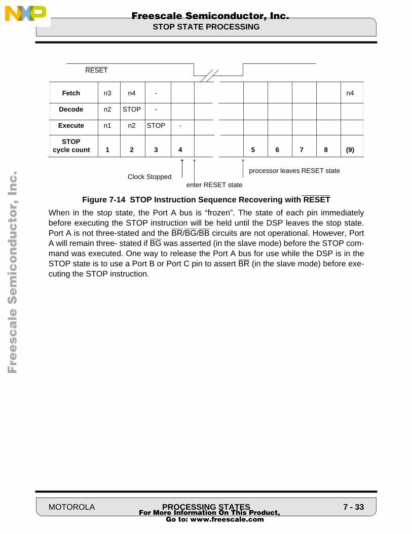
STOP STATE PROCESSING
F
ree
sca
le S
em
ico
nd
uc
tor,
I
Freescale Semiconductor, Inc.n
c..
.
When in the stop state, the Port A bus is “frozen”. The state of each pin immediatelybefore executing the STOP instruction will be held until the DSP leaves the stop state.Port A is not three-stated and the BR/BG/BB circuits are not operational. However, PortA will remain three- stated if BG was asserted (in the slave mode) before the STOP com-mand was executed. One way to release the Port A bus for use while the DSP is in theSTOP state is to use a Port B or Port C pin to assert BR (in the slave mode) before exe-cuting the STOP instruction.
Fetch n3 n4 - n4
Decode n2 STOP -
Execute n1 n2 STOP -
STOPcycle count 1 2 3 4 5 6 7 8 (9)
RESET
Clock Stoppedprocessor leaves RESET state
enter RESET state
Figure 7-14 STOP Instruction Sequence Recovering with RESET
MOTOROLA PROCESSING STATES 7 - 33 For More Information On This Product,
Go to: www.freescale.com

STOP STATE PROCESSING
F
ree
sca
le S
em
ico
nd
uc
tor,
I
Freescale Semiconductor, Inc.n
c..
.
7 - 34 PROCESSING STATES MOTOROLA For More Information On This Product,
Go to: www.freescale.com
Fre
esc
ale
Se
mic
on
du
cto
r, I
Freescale Semiconductor, Inc.n
c..
.
SECTION 8
BUS OPERATION
MOTOROLA BUS OPERATION 8 - 1 For More Information On This Product,
Go to: www.freescale.com
SECTION CONTENTS
Fre
esc
ale
Se
mic
on
du
cto
r, I
Freescale Semiconductor, Inc.n
c..
.
8.1 INTRODUCTION . . . . . . . . . . . . . . . . . . . . . . . . . . . . . . . . . . . . . . . . 8-38.2 SYNCHRONOUS BUS OPERATION . . . . . . . . . . . . . . . . . . . . . . . . . 8-38.3 BUS HANDSHAKE AND ARBITRATION . . . . . . . . . . . . . . . . . . . . . . 8-58.3.1 Bus Arbitration signals . . . . . . . . . . . . . . . . . . . . . . . . . . . . . . . . . . . . 8-58.3.2 Bus Arbitration between Two DSPs . . . . . . . . . . . . . . . . . . . . . . . . . . 8-68.3.3 Bus Arbitration between a DSP56156 and an MC68020 . . . . . . . . . . 8-78.3.4 Bus Arbitration with External Bus Arbitrator . . . . . . . . . . . . . . . . . . . . 8-9
8 - 2 BUS OPERATION MOTOROLA For More Information On This Product,
Go to: www.freescale.com

INTRODUCTION
Fre
esc
ale
Se
mic
on
du
cto
r, I
Freescale Semiconductor, Inc.n
c..
.
8.1 INTRODUCTIONDSP56100 family external bus timing is defined by the operation of the Address Bus,Data Bus, and Bus Control pins described in the User’s Manual for each of the DSPs inthe DSP56100 family. The external bus is designed to interface with a wide variety ofmemory and peripheral devices, from high speed static RAMs to slower memorydevices. Figure 8-1 shows a static RAM design using 15 ns memories.
Figure 8-1 Example of SRAM Connection to a 60 MHz DSP56156 Using One Wait-State
External bus timing is controlled by the TA control signal and by the Bus Control Regis-ters (BCR). The BCR and TA control the bus interface signal timing. Wait state insertionis controlled by the BCR to provide fixed bus access timing, and by TA to providedynamic bus access timing. The number of wait states is determined by the TA input orby the BCR, whichever is longer.
8.2 SYNCHRONOUS BUS OPERATION A synchronous external bus cycle consists of at least 4 internal clock phases. Each syn-chronous external memory access requires the following procedure:
1. The external memory address is defined by Address Bus A0-A15 and MemoryReference signal PS/DS. These signals change in the first phase of the exter-nal bus cycle. Memory Reference signal PS/DS has the same timing as theAddress Bus and may be used as an additional address line. The Address sig-nals and PS/DS are also used to generate chip select for the appropriatememory chips. Chip select changes the memory devices from low powerstandby mode to active mode and begins the read access time. This allowsslower memories to be used since the chip select signals are address basedrather than read or write enable based.
Programanddata
memory64K x 4 bits
D0-D15
A0-A14PS/DS
E
WR WEOE
DSP56156
A0-A14
D0-D15CS
TA
MCM6209-15
RD
A15
Vcc
MOTOROLA BUS OPERATION 8 - 3 For More Information On This Product,
Go to: www.freescale.com
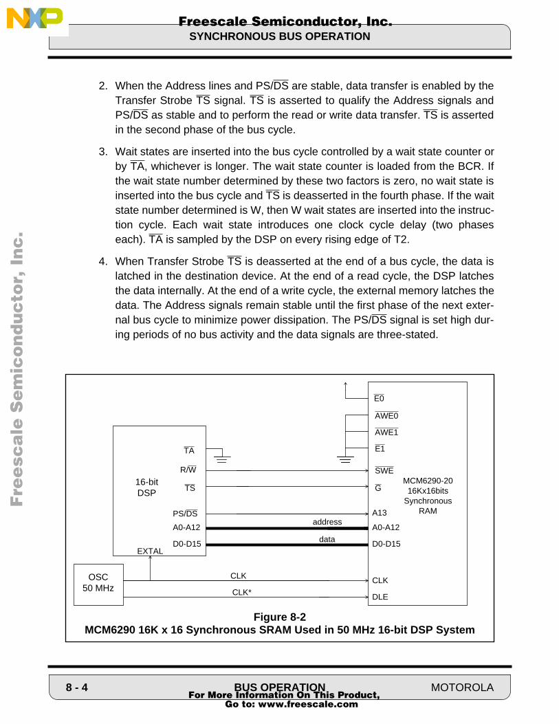
SYNCHRONOUS BUS OPERATION
Fre
esc
ale
Se
mic
on
du
cto
r, I
Freescale Semiconductor, Inc.n
c..
.
2. When the Address lines and PS/DS are stable, data transfer is enabled by theTransfer Strobe TS signal. TS is asserted to qualify the Address signals andPS/DS as stable and to perform the read or write data transfer. TS is assertedin the second phase of the bus cycle.
3. Wait states are inserted into the bus cycle controlled by a wait state counter orby TA, whichever is longer. The wait state counter is loaded from the BCR. Ifthe wait state number determined by these two factors is zero, no wait state isinserted into the bus cycle and TS is deasserted in the fourth phase. If the waitstate number determined is W, then W wait states are inserted into the instruc-tion cycle. Each wait state introduces one clock cycle delay (two phaseseach). TA is sampled by the DSP on every rising edge of T2.
4. When Transfer Strobe TS is deasserted at the end of a bus cycle, the data islatched in the destination device. At the end of a read cycle, the DSP latchesthe data internally. At the end of a write cycle, the external memory latches thedata. The Address signals remain stable until the first phase of the next exter-nal bus cycle to minimize power dissipation. The PS/DS signal is set high dur-ing periods of no bus activity and the data signals are three-stated.
MCM6290-2016Kx16bits
SynchronousRAM
data
addressPS/DS
R/W
TS
OSC50 MHz
16-bitDSP
CLK CLKCLK*
EXTAL
DLE
D0-D15
A0-A12
A13
SWE
G
TA
AWE0
AWE1
E1
E0
A0-A12
D0-D15
Figure 8-2 MCM6290 16K x 16 Synchronous SRAM Used in 50 MHz 16-bit DSP System
8 - 4 BUS OPERATION MOTOROLA For More Information On This Product,
Go to: www.freescale.com

BUS HANDSHAKE AND ARBITRATION
Fre
esc
ale
Se
mic
on
du
cto
r, I
Freescale Semiconductor, Inc.n
c..
.
Figure 8-2 shows an example of a 50 MHz 16-bit DSP connected to a 16K x 16-bit, 20ns, synchronous RAM. Note that the PS/DS control signal is used as an additionaladdress line allowing a single external memory device to be used to store both program(8k words) and data (8k words) memory.
8.3 BUS HANDSHAKE AND ARBITRATIONBus transactions are governed by a single bus master. Bus arbitration determines whichdevice becomes the bus master. The arbitration logic implementation is system depen-dent, but must result in at most one device becoming the bus master (even if multipledevices request bus ownership) at any given time.
8.3.1 Bus Arbitration signalsThree signals are provided for bus arbitration. These signals are:
BR Bus Request: Input in the slave mode; output in the master modeIn the master mode, this output is asserted by the DSP requesting the bus toindicate that the DSP wants to use the bus. The output is held asserted until theDSP no longer needs the bus. This includes when the DSP is the bus masteras well as when it is not actively using the bus but retains bus mastership.
In the slave mode, this input is asserted by an external device to indicate to theDSP that the external device wants control of the external bus. In the slavemode, when BR is asserted, the DSP always relinquishes the bus.
BG Bus Grant: Output in the slave mode; input in the master modeIn the master mode, this input is asserted by the bus arbitration controller to sig-nal the DSP that the DSP is the bus master-elect. BG is valid only when the busis not busy. The Bus Busy signal is described below.
In the slave mode, this output pin is asserted by the DSP in response to a busrequest BR. When BG is asserted, the DSP no longer drives the bus.
BB Bus Busy: Output when bus master; input when not bus masterThis pin is asserted by the device (bus master) that received bus ownershipfrom the bus arbitration controller. The master holds BB asserted for the dura-tion of its bus possession. When asserted, BB indicates that the DSP is drivingthe bus. BB deasserted indicates that the DSP is not driving the bus. BB maybe used as a three-state enable control for external address, data and bus con-trol signal buffers.
MOTOROLA BUS OPERATION 8 - 5 For More Information On This Product,
Go to: www.freescale.com

BUS HANDSHAKE AND ARBITRATION
Fre
esc
ale
Se
mic
on
du
cto
r, I
Freescale Semiconductor, Inc.n
c..
.
The BB input is monitored by the DSP when it is the potential bus master (i.e.,after BG has been asserted). The DSP will become bus master when BB isdeasserted.
Note: A DSP which is programmed as a bus master comes out of reset without pos-session of the bus. A DSP which is programmed as a bus slave comes out ofreset with possession of the bus.
8.3.2 Bus Arbitration between Two DSPsFigure 8-3 shows two DSPs sharing the same external bus. The three bus arbitrationpins BR, BG, and BB allow for direct connection without external logic. The bus arbitra-tion is explained below.
The two DSPs in Figure 8-3 share a common clock and common hardware reset cir-cuitry. DSP-1 leaves the reset state in the master mode (MC tied high) while DSP-2leaves the reset state in the slave mode (MC tied low).
Figure 8-4, Figure 8-5, and Figure 8-6 show the bus arbitration between the two proces-sors.
When DSP-1 needs the bus for an external access, BRm is asserted during T0. BGm issampled by DSP-1 during the clock’s falling edge. When BGm is asserted by DSP-2,
address
data
BRsBGsBBsMC
SharedExternalMemory
SlaveMode
BRmBGm
BB
MC
CLKRESET
control
DSP-1 DSP-2
VCC
MasterMode
Figure 8-3 Bus Arbitration Between Two 16-bit DSPs
8 - 6 BUS OPERATION MOTOROLA For More Information On This Product,
Go to: www.freescale.com

BUS HANDSHAKE AND ARBITRATION
Fre
esc
ale
Se
mic
on
du
cto
r, I
Freescale Semiconductor, Inc.n
c..
.
DSP-1 starts sampling BB on the clock’s falling edge and starts a bus cycle on theclock’s first rising edge after BB is sampled and recognized. DSP-1 then assumes busmastership by asserting BB. DSP-1 deasserts BRm when BGm has been received andthe external bus is released. BRm is deasserted during T0. BB remains asserted as longas DSP-1 drives the bus.
When DSP-2 receives a bus request on its BR input, it will three-state its A0-A15, D0-D15, TS, R/W, PS/DS pins at the earliest possible time while deasserting the BB pin. Itthen asserts BG and its BB pin becomes an input. When the BR input is deasserted,DSP-2 deasserts BG and DSP-2 regains bus control after sampling and recognizing BBas deasserted.
When the master wishes to “park” on the bus (i.e., remain master even when it is notmaking external accesses) it can set the RH bit in the BCR. This causes BR to remainasserted until the RH bit is cleared. Bus parking is illustrated in Figure 8-5.
8.3.3 Bus Arbitration between a DSP56156 and an MC68020Figure 8-7 shows a DSP in the master mode sharing the same external bus with anMC68020. The three bus arbitration pins BR, BG, and BB allow direct connection withoutexternal logic. The bus arbitration is explained below.
After hardware RESET, the DSP is set in the master mode (MC is tied is to VCC).
T0 T1 T2 Tw T2 Tw T2 Tw T2 Tw T2 Tw T2 T3 T0 T1 T2 T3 T0 T1 T2 T3 T0
T0 T1 T2 T3 T0 T1 T2 T3 T0 T1 T2 T3 T0 T1 T2 T3 T0 T1 T2 T3 T0 T1 T2
DSP-1
CLK
DSP-2
CLK
BR
BG
BB
slave drives the bus master drives the
bus
slave samples BRslave samples BR
master samples BG
master gets on the
bus
slave recognizes BR
slave grants the busmaster recognizes BG
master samplesmaster recognizes BB high
BB high
Figure 8-4 Master Requests and Gets the Bus for One Access
MOTOROLA BUS OPERATION 8 - 7 For More Information On This Product,
Go to: www.freescale.com
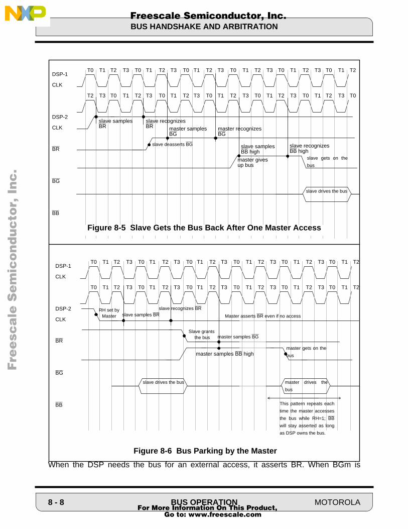
BUS HANDSHAKE AND ARBITRATION
Fre
esc
ale
Se
mic
on
du
cto
r, I
Freescale Semiconductor, Inc.n
c..
.
When the DSP needs the bus for an external access, it asserts BR. When BGm is
T0 T1 T2 T3 T0 T1 T2 T3 T0 T1 T2 T3 T0 T1 T2 T3 T0 T1 T2 T3 T0 T1 T2
T2 T3 T0 T1 T2 T3 T0 T1 T2 T3 T0 T1 T2 T3 T0 T1 T2 T3 T0 T1 T2 T3 T0
DSP-1
CLK
DSP-2
CLK
BR
BG
BB
slave drives the bus
slave deasserts BG
slave gets on the
bus
slave samplesBR
slave recognizesBR master samples master recognizes
BGBG
master givesup bus
slave samplesBB high
slave recognizesBB high
Figure 8-5 Slave Gets the Bus Back After One Master Access
Figure 8-6 Bus Parking by the Master
T0 T1 T2 T3 T0 T1 T2 T3 T0 T1 T2 T3 T0 T1 T2 T3 T0 T1 T2 T3 T0 T1 T2
T0 T1 T2 T3 T0 T1 T2 T3 T0 T1 T2 T3 T0 T1 T2 T3 T0 T1 T2 T3 T0 T1 T2
DSP-1
CLK
DSP-2
CLK
BR
BG
BB
slave drives the bus master drives the
bus
slave samples BR Master asserts BR even if no access
master samples BG
master gets on the
bus
RH set by Master
Slave grants the bus
This pattern repeats each
time the master accesses
the bus while RH=1; BB
will stay asserted as long
as DSP owns the bus.
slave recognizes BR
master samples BB high
8 - 8 BUS OPERATION MOTOROLA For More Information On This Product,
Go to: www.freescale.com

BUS HANDSHAKE AND ARBITRATION
Fre
esc
ale
Se
mic
on
du
cto
r, I
Freescale Semiconductor, Inc.n
c..
.
asserted by the MC68020, the DSP starts a bus cycle after sampling BB and BB is deas-serted. The DSP assumes bus mastership by asserting BB and then deasserts BR if itonly wants the bus for one cycle. BR remains asserted for a series of consecutive exter-nal accesses or when the bus request hold bit (RH) of the BCR register is set. BBremains asserted as long as the DSP drives the bus and as long as BG remainsasserted. When BG is deasserted, BB is deasserted at the end of the last external busaccess.
When the MC68020 receives a bus request on its BR input, it will assert BG at the earli-est possible time. BG will not be asserted until the end of a read-modify-write operation.BG will be deasserted by the MC68020 when the new bus master has asserted BGACK.
8.3.4 Bus Arbitration with External Bus ArbitratorSystems that include several devices that can become bus master require external cir-cuitry to assign priorities to the devices. This circuitry allows only the device with thehighest priority to become bus master when two or more devices attempt to become busmaster simultaneously. Figure 8-8 shows an example of bus arbitration with severalDSPs and other CPUs.
Bus arbitration is handled by a central bus arbitrator, using individual request/grant linesto each potential bus master. The arbitration protocol can operate in parallel with bustransfer activity allowing fast bus acquisition. The arbitration sequence occurs as follows:
1. All candidates for bus ownership assert their respective BR signals as soon as
address
data
SharedExternalMemory
control
DSP56156 MC68020
BRBGBGACK
BRBGBB
MC
16-bitDSPMaster
Vcc
Figure 8-7 Bus Arbitration Between a DSP56156 and an MC68020
MOTOROLA BUS OPERATION 8 - 9 For More Information On This Product,
Go to: www.freescale.com
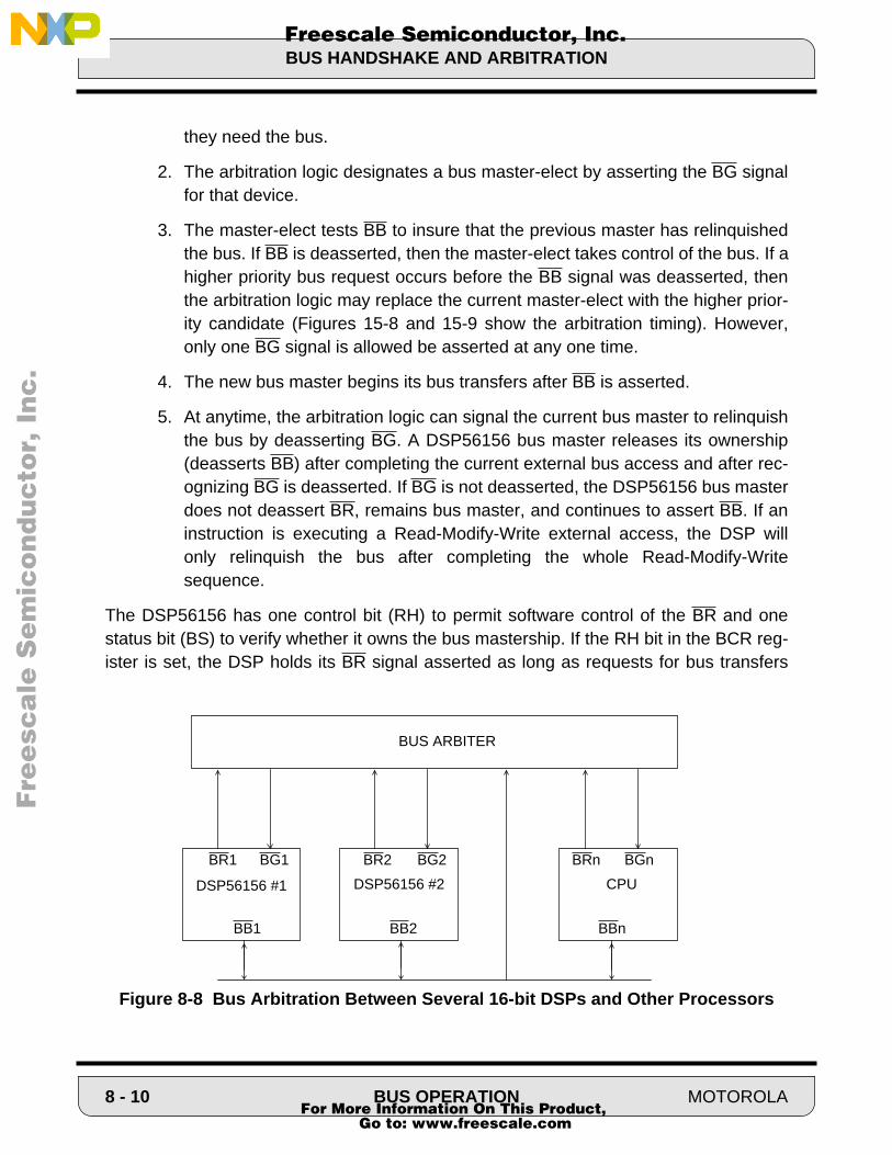
BUS HANDSHAKE AND ARBITRATION
Fre
esc
ale
Se
mic
on
du
cto
r, I
Freescale Semiconductor, Inc.n
c..
.
they need the bus.
2. The arbitration logic designates a bus master-elect by asserting the BG signalfor that device.
3. The master-elect tests BB to insure that the previous master has relinquishedthe bus. If BB is deasserted, then the master-elect takes control of the bus. If ahigher priority bus request occurs before the BB signal was deasserted, thenthe arbitration logic may replace the current master-elect with the higher prior-ity candidate (Figures 15-8 and 15-9 show the arbitration timing). However,only one BG signal is allowed be asserted at any one time.
4. The new bus master begins its bus transfers after BB is asserted.
5. At anytime, the arbitration logic can signal the current bus master to relinquishthe bus by deasserting BG. A DSP56156 bus master releases its ownership(deasserts BB) after completing the current external bus access and after rec-ognizing BG is deasserted. If BG is not deasserted, the DSP56156 bus masterdoes not deassert BR, remains bus master, and continues to assert BB. If aninstruction is executing a Read-Modify-Write external access, the DSP willonly relinquish the bus after completing the whole Read-Modify-Writesequence.
The DSP56156 has one control bit (RH) to permit software control of the BR and onestatus bit (BS) to verify whether it owns the bus mastership. If the RH bit in the BCR reg-ister is set, the DSP holds its BR signal asserted as long as requests for bus transfers
DSP56156 #1 CPU
BUS ARBITER
BR1 BR2 BRn BGnBG2BG1
BBnBB2BB1
DSP56156 #2
Figure 8-8 Bus Arbitration Between Several 16-bit DSPs and Other Processors
8 - 10 BUS OPERATION MOTOROLA For More Information On This Product,
Go to: www.freescale.com

BUS HANDSHAKE AND ARBITRATION
Fre
esc
ale
Se
mic
on
du
cto
r, I
Freescale Semiconductor, Inc.n
c..
.
are pending. As long as the RH bit is set, BR will remain asserted. This situation is called“bus parking” and allows the current bus master to use the bus repeatedly without re-arbitration.
MOTOROLA BUS OPERATION 8 - 11 For More Information On This Product,
Go to: www.freescale.com

BUS HANDSHAKE AND ARBITRATION
Fre
esc
ale
Se
mic
on
du
cto
r, I
Freescale Semiconductor, Inc.n
c..
.
8 - 12 BUS OPERATION MOTOROLA For More Information On This Product,
Go to: www.freescale.com

Fre
esc
ale
Se
mic
on
du
cto
r, I
Freescale Semiconductor, Inc.n
c..
.
SECTION 9
DSP56100 FAMILY ON-CHIP PLL
x xd∫Φ
VCO
MOTOROLA DSP56100 FAMILY ON-CHIP PLL 9 - 1 For More Information On This Product,
Go to: www.freescale.com

SECTION CONTENTS
9 - 2
DSP56100 FAMILY ON-CHIP PLL
MOTOROLA
9.1 INTRODUCTION . . . . . . . . . . . . . . . . . . . . . . . . . . . . . . . . . . . . . . . . 9-39.2 ON-CHIP CLOCK SYNTHESIS CONTROL REGISTER PCR0 . . . . . 9-49.2.1 PCR0 Feedback Divider Bits (YD7-YD0) Bits 0-7 . . . . . . . . . . . . . . . . 9-49.2.2 PCR0 Input Divider Bits (ID3-ID0) Bits 8-11 . . . . . . . . . . . . . . . . . . . . 9-59.2.3 PCR0 Power Divider Bits (PD3-PD0) Bits 12-15 . . . . . . . . . . . . . . . . 9-59.3 ON-CHIP CLOCK SYNTHESIS CONTROL REGISTER PCR1 . . . . . 9-59.3.1 PCR1 Reserved Bits — Bits 0-9 . . . . . . . . . . . . . . . . . . . . . . . . . . . . . 9-59.3.2 PCR1 CLKO Select Bits (CS1-CS0) Bits 10 and 11 . . . . . . . . . . . . . . 9-59.3.3 PCR1 Phase Select Bit (PS) Bit 12 . . . . . . . . . . . . . . . . . . . . . . . . . . . 9-69.3.4 PCR1 PLL Power Down Bit (PLLD) Bit 13 . . . . . . . . . . . . . . . . . . . . . 9-69.3.5 PCR1 PLL Enable Bit (PLLE) Bit 14 . . . . . . . . . . . . . . . . . . . . . . . . . . 9-69.3.6 PCR1 Voltage Controlled Oscillator Lock Bit (LOCK) Bit 15 . . . . . . . . 9-7
Fre
esc
ale
Se
mic
on
du
cto
r, I
Freescale Semiconductor, Inc.
For More Information On This Product, Go to: www.freescale.com
nc
...

INTRODUCTION
Fre
esc
ale
Se
mic
on
du
cto
r, I
Freescale Semiconductor, Inc.n
c..
.
9.1 INTRODUCTION
The DSP56100 Family does not contain an on-chip oscillator. An external system clockmust be provided through the EXTAL input pin. The on-chip phase locked loop (PLL) canbe used to generate the DSP5616 core system clock or it can be bypassed allowing theDSP5616 core to directly use the clock provided on the EXTAL pin.
Figure 9-1 shows the general block diagram of the on-chip frequency synthesizer.
The 4-bit divider ID3-ID0 defines the resolution of the PLL and divides the incoming clockrate fed to the PLL. The eight down counter bits YD7-YD0 control down counting in thePLL feedback loop causing it to divide by the value YD+1 (any number between 1 and256) which effectively multiplies the frequency out of the PLL. The VCO output can be di-vided down by any power of 2 between 20 and 215 before entering the core using the 4-bits PD3-PD0 of the control register PCR1. The system frequency on the DSP core is con-trolled by the frequency control bits of the PLL control register PCR0 as follows:
Fosc = Fext÷[ID+1]x[YD+1]÷ (2PD)
where ID is the value contained in ID3-ID0, YD is the value contained in YD7-YD0, andPD is the value contained in PD3-PD0. Fext is a squared and delayed version of the clocksignal applied to the EXTAL input pin.
Note: The STOP instruction does not power down the PLL if the PLL is enabled(PLLD=0) when entering the STOP mode. STOP will power down the ID register ifthe PLL is disabled (PLLD=1) when entering the STOP mode. (see Section 9.3.4).
MOTOROLA DSP56100 FAMILY ON-CHIP PLL 9 - 3 For More Information On This Product,
Go to: www.freescale.com
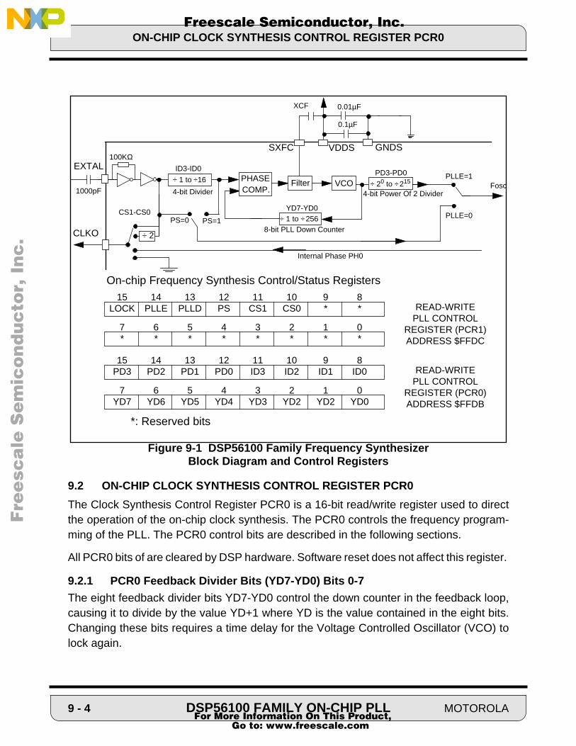
ON-CHIP CLOCK SYNTHESIS CONTROL REGISTER PCR0
Fre
esc
ale
Se
mic
on
du
cto
r, I
Freescale Semiconductor, Inc.n
c..
.
Figure 9-1 DSP56100 Family Frequency Synthesizer Block Diagram and Control Registers
9.2 ON-CHIP CLOCK SYNTHESIS CONTROL REGISTER PCR0
The Clock Synthesis Control Register PCR0 is a 16-bit read/write register used to directthe operation of the on-chip clock synthesis. The PCR0 controls the frequency program-ming of the PLL. The PCR0 control bits are described in the following sections.
All PCR0 bits of are cleared by DSP hardware. Software reset does not affect this register.
9.2.1 PCR0 Feedback Divider Bits (YD7-YD0) Bits 0-7
The eight feedback divider bits YD7-YD0 control the down counter in the feedback loop,causing it to divide by the value YD+1 where YD is the value contained in the eight bits.Changing these bits requires a time delay for the Voltage Controlled Oscillator (VCO) tolock again.
EXTAL
8-bit PLL Down Counter
PHASECOMP.
PLLE=1
PLLE=0
On-chip Frequency Synthesis Control/Status Registers15 14 13 12 11 10 9 8
LOCK PLLE PLLD PS CS1 CS0 * * READ-WRITEPLL CONTROL
REGISTER (PCR1)ADDRESS $FFDC
Fosc
YD7-YD0
VCOFilter
CLKO ÷ 2
Internal Phase PH0
CS1-CS0
100KΩ
1000pF
÷ 1 to ÷ 256
PD3-PD0
÷ 20 to ÷ 215
4-bit Power Of 2 Divider
7 6 5 4 3 2 1 0* * * * * * * *
15 14 13 12 11 10 9 8PD3 PD2 PD1 PD0 ID3 ID2 ID1 ID0 READ-WRITE
PLL CONTROLREGISTER (PCR0)ADDRESS $FFDB
7 6 5 4 3 2 1 0YD7 YD6 YD5 YD4 YD3 YD2 YD2 YD0
ID3-ID0
÷ 1 to ÷ 16
4-bit Divider
SXFC VDDS
XCF 0.01µF
GNDS
0.1µF
PS=0 PS=1
*: Reserved bits
9 - 4 DSP56100 FAMILY ON-CHIP PLL MOTOROLA For More Information On This Product,
Go to: www.freescale.com
ON-CHIP CLOCK SYNTHESIS CONTROL REGISTER PCR1
Fre
esc
ale
Se
mic
on
du
cto
r, I
Freescale Semiconductor, Inc.n
c..
.
The LOCK bit is cleared any time a new value is written to the YD bits.
The resulting DSP core system clock must be within the limits specified by the technicaldata sheet. The frequency of the VCO should also remain higher than the minimum valuespecified in this data sheet.
9.2.2 PCR0 Input Divider Bits (ID3-ID0) Bits 8-11
The four input divider bits are used to divide the input clock frequency by any number be-tween 1 and 16. The output of the divider is used as input for the phase comparator of thePLL. If ID is the value contained in the four bits, the input clock to the PLL is divided byID+1.
Any time a new value is written to the ID bits, the LOCK bit is cleared.
9.2.3 PCR0 Power Divider Bits (PD3-PD0) Bits 12-15
The four power divider bits are used to divide the VCO output clock frequency by any pow-er of two between 20 and 215 (i.e., 1, 2, 4, 8, 16, 32, …, 16384, or 32768). The output ofthe divider can be used as the operating clock for the DSP core, as shown in Figure 9-1.Writing to the PD bits does not affect the LOCK condition of the PLL.
The PD bits can be used to switch the DSP core back and forth from a high MIPS rate toa very low speed, low power mode without having to wait and check for the PLL to lockon a new frequency.
9.3 ON-CHIP CLOCK SYNTHESIS CONTROL REGISTER PCR1
The Clock Synthesis Control Register PCR1 is a 16-bit read/write register used to directthe operation of the on-chip clock synthesizer. The PCR1 control bits are described in thefollowing sections.
All PCR1 bits are cleared by DSP hardware. Software reset does not affect this register.
9.3.1 PCR1 Reserved Bits — Bits 0-9
These bits are reserved and should be written as zero by the user.
9.3.2 PCR1 CLKO Select Bits (CS1-CS0) Bits 10 and 11
The two CLKO Select bits CS1-CS0 enable one of three possible clocks to be output tothe CLKO pin when the CD bit in the OMR register is cleared (see Figure 9-1). After hard-ware reset, the internal DSP core clock PH0 (phase zero) is output to the CLKO pin. PH0is a delayed version of the DSP core master clock, Fosc. Changing the value of the twobits CS1-CS0 according to Table 9-1, Fext or Fext/2 can be selected to be output on CL-KO. Fext is a squared and delayed version of the signal applied to the EXTAL input pin.
MOTOROLA DSP56100 FAMILY ON-CHIP PLL 9 - 5 For More Information On This Product,
Go to: www.freescale.com

ON-CHIP CLOCK SYNTHESIS CONTROL REGISTER PCR1
Fre
esc
ale
Se
mic
on
du
cto
r, I
Freescale Semiconductor, Inc.n
c..
.
9.3.3 PCR1 Phase Select Bit (PS) Bit 12
This bit is used to select the DSP core clock when the PLL output is not selected(PLLE=0). When this bit is cleared, a squared version of EXTAL is selected as Fosc.When this bit is set, the output of the ID divider is selected as Fosc.
9.3.4 PCR1 PLL Power Down Bit (PLLD) Bit 13
When the PLLD bit is set, the on-chip PLL is powered down. When this control bit iscleared, the on-chip PLL is turned on. This bit should not be set when the PLLE bit is set.
If the PLL has to be turned off before entering the STOP mode, the following sequencewill have to be executed before the STOP instruction:
- Clear the PLLE bit (switch back to EXTAL)- Set the PLLD bit (power down the PLL)- Execute the STOP instruction.
Setting the PLLD bit clears the LOCK bit. Setting the PLLD bit powers down the completePLL block including the PD and YD registers.
9.3.5 PCR1 PLL Enable Bit (PLLE) Bit 14
When the PLLE bit is set, the DSP5616 core system clock is generated by the on-chipPLL. Table 9-2 summarizes the function of the three bits — PLLE, PLLD and PS. Thestate of the PLL is defined by the PLLD bit. When the PLLD bit is set, the PLL is in thepower down mode. When the PLLD bit is cleared, the PLL is in the active mode. Beforeturning the PLL off, the PLLE bit should be cleared in order to by-pass the PLL. The PLLcan then be put in power down mode by setting PLLD.
If the output frequency of the PLL has to be changed by re-programming the YD bits whilethe PLL output is used by the core (PLLE=1; PLLD=0), the following sequence of opera-tions should be performed:
- Clear the PLLE bit to switch back to EXTAL
Table 9-1 CLKOUT Pin Control
CS1 CS0 CLKO
0 0 PH0
0 1 Reserved
1 0 Fext
1 1 Fext/2
9 - 6 DSP56100 FAMILY ON-CHIP PLL MOTOROLA For More Information On This Product,
Go to: www.freescale.com

ON-CHIP CLOCK SYNTHESIS CONTROL REGISTER PCR1
Fre
esc
ale
Se
mic
on
du
cto
r, I
Freescale Semiconductor, Inc.n
c..
.
- Program the YD bits (only after clearing PLLE)- Wait for the LOCK bit to be set- Set PLLE after the LOCK bit is tested high.
9.3.6 PCR1 Voltage Controlled Oscillator Lock Bit (LOCK) Bit 15
This status bit shows whether the Voltage Controlled Oscillator (VCO) has locked on thedesired frequency or not. When the LOCK bit is set, the VCO has locked; when the LOCKbit is cleared, the VCO has not locked yet. This bit is cleared when setting the PLLD bitand when changing the value of ID or YD bits. The LOCK bit is not cleared when clearingthe PLLE bit without changing the values of PLLD, YD, or ID.
This bit is read-only and cannot be written by the DSP core.
Table 9-2 PLL Operations
PLLE PLLD PS Fosc PLL Mode
0 0 0 Fext Active
0 1 0 Fext Power Down
0 0 1 Fext÷[ID+1] Active
0 1 1 Fext÷[ID+1] Power Down
1 0 x Fext÷[ID+1]x[YD+1]÷ (2PD) Active
1 1 x Reserved —
MOTOROLA DSP56100 FAMILY ON-CHIP PLL 9 - 7 For More Information On This Product,
Go to: www.freescale.com

ON-CHIP CLOCK SYNTHESIS CONTROL REGISTER PCR1
Fre
esc
ale
Se
mic
on
du
cto
r, I
Freescale Semiconductor, Inc.n
c..
.
Figure 9-2 On-Chip Frequency Synthesizer Programming Model Summary.
On-chip Frequency Synthesis Control/Status Register (PCR1) ADDRESS X:$FFDC
15 14 13 12 11 10 9 8 7 6 5 4 3 2 1 0LOCK PLLE PLLD PS CS1 CS0 ** ** ** ** ** ** ** ** ** **
LOCK 0 PLL unlocked 1 PLL locked
PLLE PLLD 00 PLL active but not used as Fosc 01 PLL powered down 10 PLL active and used as Fosc 11 Reserved
PHASE 0 Squared EXTAL selected as Fosc if PLLE=0 SELECT 1 Squared EXTAL/ID selected as Fosc if PLLE=0 CS1-CS0 00 PH0 output to CLKO when enabled by the CD bit (bit 7) of the OMR
CLKO 01 reservedSelect 10 Fext output to CLKO when enabled by the CD bit (bit 7) of the OMR
11 Fext/2 output to CLKO when enabled by the CD bit (bit 7) of the OMR
EXTAL
8-bit PLL Down Counter
PHASECOMP.
PLLE=1
PLLE=0
Fosc
YD7-YD0
VCOFilter
CLKO ÷ 2
Internal Phase PH0
CS1-CS0÷ 1 to ÷ 256
PD3-PD0
÷ 20 to ÷ 215
4-bit Power of two Divider
On-chip Frequency Synthesis Control/Status Register (PCR0) ADDRESS X:$FFDB
15 14 13 12 11 10 9 8 7 6 5 4 3 2 1 0PD3 PD2 PD1 PD0 ID3 ID2 ID1 ID0 YD7 YD6 YD5 YD0 YD3 YD2 YD1 YD0
ID3-ID0
÷ 1 to ÷ 16
4-bit Divider
PD3-PD0 $0 Divide the VCO output clock by 1 (20) 8 Divide the VCO output clock by 256 (28)
Clock $1 Divide the VCO output clock by 2 (21) 9 Divide the VCO output clock by 512 (29)
Output $2 Divide the VCO output clock by 4 (22) A Divide the VCO output clock by 1024 (210)
Divider $3 Divide the VCO output clock by 8 (23) B Divide the VCO output clock by 2048 (211)
$4 Divide the VCO output clock by 16 (24) C Divide the VCO output clock by 4096 (212)
$5 Divide the VCO output clock by 32 (25) D Divide the VCO output clock by 8192 (213)
$6 Divide the VCO output clock by 64 (26) E Divide the VCO output clock by 16384 (214)
$7 Divide the VCO output clock by 128 (27) F Divide the VCO output clock by 32768 (215)ID3-ID0 $0 Divide the input clock by 1 8 Divide the input clock by 9
Input $1 Divide the input clock by 2 9 Divide the input clock by 10Clock $2 Divide the input clock by 3 A Divide the input clock by 11
Divider $3 Divide the input clock by 4 B Divide the input clock by 12$4 Divide the input clock by 5 C Divide the input clock by 13$5 Divide the input clock by 6 D Divide the input clock by 14$6 Divide the input clock by 7 E Divide the input clock by 15$7 Divide the input clock by 8 F Divide the input clock by 16
YD7-YD0VCODown $YD Multiplies by YD+1
Countervalue
PS=0 PS=1
9 - 8 DSP56100 FAMILY ON-CHIP PLL MOTOROLA For More Information On This Product,
Go to: www.freescale.com

Fre
esc
ale
Se
mic
on
du
cto
r, I
Freescale Semiconductor, Inc.n
c..
.
SECTION 10
ON-CHIP EMULATION (OnCE)
MOTOROLA ON-CHIP EMULATION (OnCE) 10 - 1 For More Information On This Product,
Go to: www.freescale.com

SECTION CONTENTS
Fre
esc
ale
Se
mic
on
du
cto
r, I
Freescale Semiconductor, Inc.n
c..
.
10.1 INTRODUCTION . . . . . . . . . . . . . . . . . . . . . . . . . . . . . . . . . . . . . . . . 10-310.2 EMULATION AND TEST PINOUT . . . . . . . . . . . . . . . . . . . . . . . . . . . 10-310.3 ONCE CONTROLLER AND SERIAL INTERFACE . . . . . . . . . . . . . . 10-510.4 OnCE BREAKPOINT LOGIC . . . . . . . . . . . . . . . . . . . . . . . . . . . . . . . 10-910.5 TRACE/STEP MODE . . . . . . . . . . . . . . . . . . . . . . . . . . . . . . . . . . . . . 10-1110.6 METHODS OF ENTERING THE DEBUG MODE . . . . . . . . . . . . . . . . 10-1210.7 PIPELINE INFORMATION . . . . . . . . . . . . . . . . . . . . . . . . . . . . . . . . . 10-1410.8 PAB HISTORY BUFFER . . . . . . . . . . . . . . . . . . . . . . . . . . . . . . . . . . 10-1510.9 SERIAL PROTOCOL DESCRIPTION . . . . . . . . . . . . . . . . . . . . . . . . 10-1810.10 DSP56100 TARGET SITE DEBUG SYSTEM REQUIREMENTS . . . 10-2010.11 USING THE OnCE . . . . . . . . . . . . . . . . . . . . . . . . . . . . . . . . . . . . . . . 10-21
10 - 2 ON-CHIP EMULATION (OnCE) MOTOROLA For More Information On This Product,
Go to: www.freescale.com

INTRODUCTION
Fre
esc
ale
Se
mic
on
du
cto
r, I
Freescale Semiconductor, Inc.n
c..
.
10.1 INTRODUCTION
The purpose of this Section is to describe a set of circuits which will be used for hardware/software emulation and debug on the DSP56100 family. OnCE provides a means of inter-acting with the DSP and any memory mapped peripherals non-intrusively so that a usermay examine registers, memory or on-chip peripherals. To achieve this, special circuitsand dedicated pins on the DSP are used to avoid sacrificing any user accessible on-chipresource. A key feature of the special OnCE pins is to allow the user to insert the DSP intohis target system yet retaining debug control, especially in the cases of devices specifiedwithout external bus. The need for a costly cable which brings out the footprint of any chipon traditional emulator systems is eliminated.
Figure 10-1 illustrates a block diagram of the Emulation and test serial interface.
10.2 EMULATION AND TEST PINOUT
10.2.1 Debug Serial Input/OnCE Status 0 (DSI/OS0)
The DSI/OS0 pin, when input, is the pin through which serial data or commands are pro-vided to the OnCE controller. The data received on the DSI pin is recognized only whenthe DSP has entered the debug mode of operation. Data is always shifted into the OnCEserial port most significant bit (MSB) first on the falling edge of the OnCE serial clock,DSCK. When an output, this pin in conjuction with the OS1 pin, provides information aboutthe chip status when debug mode cannot be entered in response to an external request.The DSI/OS0 pin is an output when not in Debug Mode (i.e., until the acknowledge signalis issued to the Command Controller). When switching from output to input, the pin isthree-stated. In order to avoid any possible glitches, an external pull-down resistor shouldbe attached to this pin. During hardware reset, this pin is defined as an output and it isdriven low.
10.2.2 Debug Serial Clock/OnCE Status 1 (DSCK/OS1)
The DSCK/OS1 pin, when an input, is the pin through which the serial clock is supplied tothe OnCE controller. The serial clock provides pulses required to shift data into and out ofthe OnCE serial port. Data is shifted into the chip via the DSI pin on the falling edge ofDSCK and is shifted out of the chip via the DSO pin on the rising edge of DSCK. Whenan output, this pin, in conjunction with the OS0 pin, provides information about the chipstatus when debug mode cannot be entered in response to an external request. TheDSCK/OS1 pin is an output when not in Debug Mode (until the acknowledge signal is is-sued to the Command Controller). When switching from output to input, the pin is firstthree-stated. In order to avoid any possible glitches, an external pull-down resistor shouldbe attached to this pin. During hardware reset, this pin is defined as output and it is drivenlow.
MOTOROLA ON-CHIP EMULATION (OnCE) 10 - 3 For More Information On This Product,
Go to: www.freescale.com
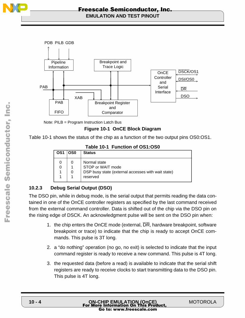
EMULATION AND TEST PINOUT
Fre
esc
ale
Se
mic
on
du
cto
r, I
Freescale Semiconductor, Inc.n
c..
.
Table 10-1 shows the status of the chip as a function of the two output pins OS0:OS1.
Table 10-1 Function of OS1:OS0
10.2.3 Debug Serial Output (DSO)
The DSO pin, while in debug mode, is the serial output that permits reading the data con-tained in one of the OnCE controller registers as specified by the last command receivedfrom the external command controller. Data is shifted out of the chip via the DSO pin onthe rising edge of DSCK. An acknowledgment pulse will be sent on the DSO pin when:
1. the chip enters the OnCE mode (external, DR, hardware breakpoint, softwarebreakpoint or trace) to indicate that the chip is ready to accept OnCE com-mands. This pulse is 3T long.
2. a “do nothing” operation (no go, no exit) is selected to indicate that the inputcommand register is ready to receive a new command. This pulse is 4T long.
3. the requested data (before a read) is available to indicate that the serial shiftregisters are ready to receive clocks to start transmitting data to the DSO pin.This pulse is 4T long.
OnCEController
and Serial
Interface
Breakpoint and Trace Logic
Pipeline Information
PAB
FIFO
Breakpoint Registerand
Comparator
DSCK/OS1
DSI/OS0
DR
DSO
PILBPDB GDB
PAB
XAB
Note: PILB = Program Instruction Latch Bus
Figure 10-1 OnCE Block Diagram
OS1 OS0 Status
0 0 Normal state0 1 STOP or WAIT mode1 0 DSP busy state (external accesses with wait state)1 1 reserved
10 - 4 ON-CHIP EMULATION (OnCE) MOTOROLA For More Information On This Product,
Go to: www.freescale.com
ONCE CONTROLLER AND SERIAL INTERFACE
Fre
esc
ale
Se
mic
on
du
cto
r, I
Freescale Semiconductor, Inc.n
c..
.
4. the shift registers are ready to receive clocks to receive data (before a write)from the DSI pin. This pulse is 4T long.
5. the shift registers have finished shifting in the new data (after a write) to indi-cate that the input command register is now ready to receive new instruction.This pulse is 4T long.
6. an instruction has completed execution (go, no exit; repeat an instruction).This pulse is 4T long.
Data is always shifted out the OnCE serial port most significant bit (MSB) first on the risingedge of DSCK. When not in debug mode, the DSO pin is driven high. During hardwarereset this pin is driven high.
10.2.4 Debug Request Input (DR)
The DR input is an active low pin that provides a means of entering the debug mode ofoperation from the external command controller. This pin, when asserted, will cause theDSP to finish the current instruction being executed, save the instruction pipeline informa-tion, enter the debug mode and wait for commands to be entered from the debug serialinput line.
10.3 ONCE CONTROLLER AND SERIAL INTERFACE
The OnCE Controller and Serial Interface contains the following blocks: input shift regis-ter, bit counter, OnCE decoder and the status/control register. Figure 10-2 illustrates ablock diagram of the OnCE serial interface.
10.3.1 OnCE Input Shift Register (OISR)
The OISR is an 8-bit shift register that receives the serial data from the DSI line. The datais clocked into the register on the falling edge of the clock applied to the DSCK pin. Afterthe 8th bit is received the OISR will stop shifting in new data. The latched data will be usedas input for the OnCE Decoder. The data is always shifted into the OISR most significantbit (MSB) first.
10.3.2 OnCE Bit Counter (OBC)
The OBC is a 4-bit counter (0…15) associated with shifting in and out the data bits. TheOBC is incremented by the falling edges of the DSCK. The OBC is cleared at reset andwhenever the DSP acknowledges that the Debug Mode has been entered. The OBC sup-plies two signals to the OnCE Decoder: one indicating that the first 8 bits were shifted-in(so a new command is available) and the second indicating that 16 bits were shifted-in(the data associated with that command is available) or that 16 bits were shifted-out (thedata required by a read command was shifted out).
MOTOROLA ON-CHIP EMULATION (OnCE) 10 - 5 For More Information On This Product,
Go to: www.freescale.com

ONCE CONTROLLER AND SERIAL INTERFACE
Fre
esc
ale
Se
mic
on
du
cto
r, I
Freescale Semiconductor, Inc.n
c..
.
10.3.3 OnCE Decoder (ODEC)
The ODEC is the supervisor of the entire OnCE activity. It receives as input the 8-bit com-mand from the OISR, two signals from OBC (one indicating that 8 bits have been receivedand the other that 16 bits have been received), and one signal indicating that the DSP hashalted. The ODEC generates all the strobes required for reading and writing the selectedOnCE registers.
10.3.4 OnCE Status and Control Register (OSCR)
The (OSCR is a 16-bit register used to select the events that will put the chip in DebugMode. Breakpoints may be disabled or enabled on one memory space. The Trace Modeof operation is also selected through OSCR.
OSCR is shown in Table 10-2 and the control bits are described in the following para-graphs.
BIT7
SER_OUT (DSO)
SER_IN (DSI)
CLK_IN (DSCK)
Status and Control Register(OSCR)
OnCEDecoder(ODEC)
Bit Counter(OBC)
BIT7
STR
STW
REGREAD REGWRITE
MODE SELECT
ISDEBUG
ISBKPT
ISSWDBG
ISHWDBG
ISTRACE
(DR)
8-bit register
4-bit counter
16-bit register
OnCE InputShift Register
(OISR)
BIT15
Note: ISxxxx = Interrupt Service xxxx
Figure 10-2 OnCE Controller and Serial Interface
10 - 6 ON-CHIP EMULATION (OnCE) MOTOROLA For More Information On This Product,
Go to: www.freescale.com

ONCE CONTROLLER AND SERIAL INTERFACE
Fre
esc
ale
Se
mic
on
du
cto
r, I
Freescale Semiconductor, Inc.n
c..
.
Table 10-2 OnCE Status and Control Register (OSCR)
10.3.4.1 OSCR Breakpoint Enables (BE0-BE1) Bit 0-1
These control bits enable or disable the breakpoint logic and select the type of memoryoperations (read; write; access) upon which the breakpoint logic operates. These bits arecleared on hardware reset.
10.3.4.2 OSCR Breakpoint Selection (BS0-BS1) Bits 2-3
These control bits select if the Breakpoints will be recognized on program memory fetch,program memory access, X memory access or second X memory read. These bits arecleared on hardware reset.
15 14 13 12 11 10 9 8 7 6 5 4 3 2 1 0
ControlStatus
* * * * * TO HBO SBO * * * TME BS1 BS0 BE1 BE0
BE1 BE0 Selection
0 0 Breakpoint disabled0 1 Breakpoint enabled on memory write1 0 Breakpoint enabled on memory read1 1 Breakpoint enabled on memory access
BS1 BS0 Selection
0 0 Breakpoint on program memory fetch (fetch of the first word of instructions whichare actually executed; not of those which are killed, not of those which are the sec-ond word of two-word instructions, and not of jumps which are not taken)
0 1 Breakpoint on any program memory access (any MOVEM instructions, fetches ofinstructions which are executed and of instructions which are killed, fetches of sec-ond word of two-word instructions, and fetches of jumps which are not taken
1 0 Breakpoint on first X memory (xab1) access
1 1 Breakpoint on second X memory (xab2) read(xab2 cannot be used to write data into the X memory)
MOTOROLA ON-CHIP EMULATION (OnCE) 10 - 7 For More Information On This Product,
Go to: www.freescale.com

ONCE CONTROLLER AND SERIAL INTERFACE
Fre
esc
ale
Se
mic
on
du
cto
r, I
Freescale Semiconductor, Inc.n
c..
.
The decoding scheme for BS(1:0) and BE(1:0) is as follows:
10.3.4.3 OSCR Trace Mode Enable (TME) Bit 4
This control bit, when set, enables the Trace Mode. When the Trace Mode is enabled, thechip will enter the Debug Mode whenever the execution of an instruction is completed andthe Trace Counter is zero. This bit is cleared on hardware reset.
10.3.4.4 OSCR (Reserved) Bits 5-7
These bits are reserved for future use and read as zero. Reserved bits should be writtenas zero for future compatibility.
10.3.4.5 OSCR Software Breakpoint Occurrence (SBO) Bit 8
This read-only status bit is set when the debug mode has been entered by a DEBUG orDEBUGcc instruction. It is used by the external command controller to determine how thedebug mode was entered. This bit is cleared when leaving the debug mode and is alsocleared on hardware reset.
10.3.4.6 OSCR Hardware Breakpoint Occurrence (HBO) Bit 9
This read-only status bit is set when a OnCE hardware breakpoint occurs. It is used bythe external command controller to determine how the debug mode was entered. This bitis cleared when leaving the debug mode and it is also cleared on hardware reset.
Function BS(1:0) BE(1:0)
disable XX 00
program fetch 00 01program fetch 00 10program fetch 00 11
any program write or fetch 01 01any program read or fetch 01 10any program access or fetch 01 11
XAB1 write 10 01XAB1 read 10 10XAB1 access 10 11
disable 11 01XAB2 read 11 10XAB2 read 11 11
10 - 8 ON-CHIP EMULATION (OnCE) MOTOROLA For More Information On This Product,
Go to: www.freescale.com

OnCE BREAKPOINT LOGIC
Fre
esc
ale
Se
mic
on
du
cto
r, I
Freescale Semiconductor, Inc.n
c..
.
10.3.4.7 OSCR Trace Occurrence (TO) Bit 10
This read-only status bit is set when the debug mode of operation is entered from a dec-rement to zero of the trace counter and the trace mode has been armed. This bit is clearedon reset and when leaving the debug mode.
10.3.4.8 OSCR Reserved – Bits 11-15
These bits are reserved for future use and read as zero. Reserved bits should be writtenas zero for future compatibility.
10.4 OnCE BREAKPOINT LOGIC
Other processors traditionally set a breakpoint in program memory by replacing the in-struction at the breakpoint address with an illegal instruction which causes a breakpointexception. This technique is limiting in that breakpoints can only be set in RAM at the be-ginning of an opcode and not on an operand. Using such techniques, breakpoints cannever be set in data memory.
On the other hand, by using address comparators, breakpoints may be set on programmemory opcodes or any data memory location. This significantly increases the program-mer’s ability to monitor what the program is doing real-time.
The breakpoint logic can be enabled for Program memory breakpoints or for Data memorybreakpoints. It contains an address latch, a register that stores the breakpoint address, acomparator and a counter. Figure 10-3 illustrates a block diagram of the OnCE BreakpointLogic.
10.4.1 OnCE Breakpoint Logic Operation
The address comparator register is useful in halting a program at a specific point to ex-amine/change registers or memory. Using the address comparator to set breakpoints en-ables the user to set breakpoints in RAM or ROM while in any operating mode.
The address comparator will cause a logic true signal when the comparison of its value isequal to the address on the bus. The breakpoint counter is then decremented if greaterthan zero. If the breakpoint counter is equal to zero, it is not decremented and a break-point occurs.
Conditional jump addresses produced by the instruction pipeline that are equal to the pro-gram address being monitored are only valid if the conditional jump instruction occurs,otherwise the conditional jump address is ignored. Program memory address breakpointsoccur after the opcode or operand is executed and the breakpoint counter has been dec-remented to zero.
MOTOROLA ON-CHIP EMULATION (OnCE) 10 - 9 For More Information On This Product,
Go to: www.freescale.com
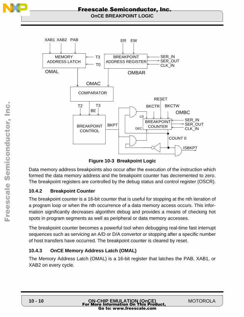
OnCE BREAKPOINT LOGIC
Fre
esc
ale
Se
mic
on
du
cto
r, I
Freescale Semiconductor, Inc.n
c..
.
Data memory address breakpoints also occur after the execution of the instruction whichformed the data memory address and the breakpoint counter has decremented to zero.The breakpoint registers are controlled by the debug status and control register (OSCR).
10.4.2 Breakpoint Counter
The breakpoint counter is a 16-bit counter that is useful for stopping at the nth iteration ofa program loop or when the nth occurrence of a data memory access occurs. This infor-mation significantly decreases algorithm debug and provides a means of checking hotspots in program segments as well as peripheral or data memory accesses.
The breakpoint counter becomes a powerful tool when debugging real-time fast interruptsequences such as servicing an A/D or D/A convertor or stopping after a specific numberof host transfers have occurred. The breakpoint counter is cleared by reset.
10.4.3 OnCE Memory Address Latch (OMAL)
The Memory Address Latch (OMAL) is a 16-bit register that latches the PAB, XAB1, orXAB2 on every cycle.
BREAKPOINTCOUNTER
MEMORYADDRESS LATCH
COMPARATOR
BREAKPOINTCONTROL
PABXAB1
T3
T0
EWER
SER_INSER_OUTCLK_IN
T3T2BE
BKPT
BREAKPOINTADDRESS REGISTER
SER_INSER_OUTCLK_IN
BKCTR
RESET
BKCTW
LD
DEC
COUNT 0
ISBKPT
OMAL OMBAR
OMAC
OMBC
XAB2
Figure 10-3 Breakpoint Logic
10 - 10 ON-CHIP EMULATION (OnCE) MOTOROLA For More Information On This Product,
Go to: www.freescale.com

TRACE/STEP MODE
Fre
esc
ale
Se
mic
on
du
cto
r, I
Freescale Semiconductor, Inc.n
c..
.
10.4.4 Memory Breakpoint Address Register (OMBAR)
The Memory Breakpoint Address Register (OMBAR) is a 16-bit register that stores thememory breakpoint address. OMBAR is available for read/write operations only throughthe OnCE serial interface. Before enabling breakpoints, OMBAR must be loaded by thecommand controller.
10.4.5 Memory Address Comparator (OMAC)
The Memory Address Comparator (OMAC) is a 16-bit comparator that compares the cur-rent memory address (stored by OMAL) with Memory Address Register (OMBAR). IfOMAC is equal to OMAL then the comparator delivers a signal indicating that the break-point address has been reached.
10.4.6 Memory Breakpoint Counter (OMBC)
The Program Memory Breakpoint Counter (OMBC) is a 16-bit counter which is loadedwith a value equal to the number of times minus one that a program or data memory ad-dress should occur before a breakpoint is acknowledged. On each occurrence the counteris decremented. When the counter has reached the value of zero and a new occurrencetakes place, a signal is generated and, if breakpoints are enabled in OSCR, the chip willenter the Debug Mode. OMBC is available for read/write operations only through theOnCE serial interface. Before enabling Memory Breakpoints, OMBC must be loaded bythe command controller.
10.5 TRACE/STEP MODE
When in the special trace mode, the DSP will not cause an interrupt exception but insteadwill enter the debug operation mode and wait for further instructions from the debug serialport. Single or multiple instructions can be traced.
10.5.1 Trace Counter
The trace mode has a 16-bit counter associated with it so that more than one instructionmay be executed before returning back to the debug mode of operation. The objective ofthe counter is to allow the user to take multiple instruction steps in real-time with no inter-ference from the debug mode. This feature helps the software developer debug sectionsof code which do not have a normal flow or are getting hung up in infinite loops. The tracecounter also enables the user to debug areas of code which are time critical.
To enable the trace mode of operation the counter is loaded with a value, the programcounter is set to the start location of the instruction(s) to be executed real-time, the tracemode is selected in the debug status register (OSCR) and the DSP exits the debug modeby executing the appropriate command issued by the external command controller. Upon
MOTOROLA ON-CHIP EMULATION (OnCE) 10 - 11 For More Information On This Product,
Go to: www.freescale.com

METHODS OF ENTERING THE DEBUG MODE
Fre
esc
ale
Se
mic
on
du
cto
r, I
Freescale Semiconductor, Inc.n
c..
.
exiting the debug mode the counter is decremented after each execution of an instruction.Interrupts are serviceable and all instructions executed including fast interrupt serviceswill decrement the trace counter. Upon decrementing to zero the DSP will re-enter the de-bug mode, the trace occurrence bit in the debug status/control register (OSCR) will be setand the debug serial output pin DSO will be toggled to indicate that the DSP OnCE portis requesting service.
Note: The trace count should be loaded with one less than (i.e., N-1) the number of in-structions that the user wants to execute (e.g., to single step one instruction, thetrace counter is loaded with a zero).
The Trace counter is cleared by hardware reset. Figure 10-4 illustrates a block diagramof the Trace Counter logic.
10.6 METHODS OF ENTERING THE DEBUG MODE
Entering the Debug Mode is acknowledged by the chip by toggling the DSO line for 3 Tcycles. This informs the external command controller that the chip has entered the DebugMode and is waiting for commands. There are seven ways in which the Debug Mode maybe entered. They are:
1. External Request During Hardware Reset
2. External Request During Normal Activity
3. External Request During STOP
4. External Request During WAIT
5. Software Request During Normal Activity
6. Enabling Trace Mode
7. Enabling Breakpoints
10.6.1 External Request During Hardware Reset
Holding the DR line asserted during the assertion of RESET will cause the chip to enterthe Debug Mode. After receiving the acknowledge, the command controller must deassertthe DR line. Note that in this case the chip does not perform any fetch or memory accessbefore entering the Debug Mode.
10.6.2 External Request During Normal Activity
Holding the DR line asserted during the normal chip activity will cause the chip to finishexecution of the current instruction and then enter the Debug Mode. After receiving the
10 - 12 ON-CHIP EMULATION (OnCE) MOTOROLA For More Information On This Product,
Go to: www.freescale.com

METHODS OF ENTERING THE DEBUG MODE
Fre
esc
ale
Se
mic
on
du
cto
r, I
Freescale Semiconductor, Inc.n
c..
.
acknowledge the command controller must deassert the DR line. Note that in this casethe chip completes execution of the current instruction and stops after the newly fetchedinstruction enters the instruction latch. This process is the same for any newly fetched in-struction including instructions fetched during interrupt processing or instructions that willbe killed by the interrupt processing.
10.6.3 External Request During STOP
Asserting DR when the chip is in the stop state (i.e., it has executed a STOP instruction)causes the chip to exit the stop state and enter the Debug Mode. The chip will wake upfrom the stop state normally (finish executing STOP) and halt after the next instruction en-ters the instruction latch. After receiving the acknowledge, the command controller mustdeassert DR. Note that in this case the chip completes the execution of the STOP instruc-tion and halts after the next instruction enters the instruction latch.
10.6.4 External Request During WAIT
Asserting DR when the chip is in the wait state (i.e. has executed a WAIT instruction)causes the chip to exit wait state and enter the Debug Mode. The chip will wake up fromthe wait state normally (finish executing WAIT) and halt after the next instruction entersthe instruction latch. After receiving the acknowledge, the command controller must deas-sert DR. Note that in this case the chip completes execution of the WAIT instruction andhalts after the next instruction enters the instruction latch.
10.6.5 Software Request During Normal Activity
Upon executing the DEBUG or DEBUGcc instructions (with condition true for DEBUGcc),the chip will enter Debug Mode after the instruction following the DEBUG/DEBUGcc in-struction has entered the instruction latch.
TRACECOUNTEREND OF
SER_INSER_OUTCLK_IN
TRCTR
RESET
TRCTW
LD
DEC
COUNT 0
ISTRACE
INSTRUCTION
Figure 10-4 Trace Counter Logic
MOTOROLA ON-CHIP EMULATION (OnCE) 10 - 13 For More Information On This Product,
Go to: www.freescale.com
PIPELINE INFORMATION
Fre
esc
ale
Se
mic
on
du
cto
r, I
Freescale Semiconductor, Inc.n
c..
.
10.6.6 Enabling Trace Mode
When the chip is operating in Trace Mode and the Trace Counter reaches a value of zero,the chip will enter the Debug Mode after completing execution of the instruction thatcaused the Trace Counter to decrement. Only those instructions that are actually execut-ed may cause the Trace Counter to decrement i.e. a killed instruction (instruction discard-ed during the interrupt process) will not decrement the Trace Counter and will not causethe chip to enter the Debug Mode.
10.6.7 Enabling Breakpoints
The chip will enter the Debug Mode after completing execution of the instruction thatcaused the Breakpoint Counter to decrement when:
1. operating in the Trace Mode when the Breakpoint Counter has reached zero
or
2. when operating in Normal Mode with the Breakpoint mechanism enabled andthe Breakpoint Counter has reached zero.
In the case of breakpointing on:
1. Program memory addresses, the breakpoint will be acknowledged immedi-ately after the execution of the instruction accessed at the specified address.
2. Data memory addresses the breakpoint will be acknowledged after the com-pletion of the instruction following the instruction that caused the access at thespecified address.
10.7 PIPELINE INFORMATION
The previous chip pipeline state must be reconstructed to resume normal chip activitywhen returning from the Debug Mode. Figure 10-5 illustrates a block diagram of PipelineInformation Registers. Only the PDB register and the PIL register are used to reconstructthe pipeline as it was before debug. the PAB History Buffer, PAB Register for Fetch andPAB Register for Decode are only used for status information. When loading a one wordinstruction into the PDB and issuing a GO command, the hardware internally transfers thePDB to the PIL and then executes the instruction. When loading a two word instruction,the first word is loaded into the PDB. As the second word is loaded to the PDB, the firstword is automatically transferred to the PIL and then execution takes place.
10 - 14 ON-CHIP EMULATION (OnCE) MOTOROLA For More Information On This Product,
Go to: www.freescale.com

PAB HISTORY BUFFER
Fre
esc
ale
Se
mic
on
du
cto
r, I
Freescale Semiconductor, Inc.n
c..
.
10.7.1 OnCE PDB Register (OPDBR)
The PDB Register (OPDBR) is a read/write, 16-bit latch that stores the value of the Pro-gram Data Bus generated by the last Program Memory access of the DSP before the De-bug Mode is entered. OPDBR is available for read/write operations only through the serialinterface. This register is affected by the operations performed during the Debug Modeand must be restored by the command controller when returning to normal mode.
10.7.2 OnCE PIL Register (OPILR)
The OPILR is a read only 16-bit latch that stores the instruction present in the InstructionLatch when the Debug Mode is entered. OPILR is available for read operations onlythrough the serial interface. If a write is selected for this register, i.e., R/W = 0 and RS4-RS0 = 01011, then zeros will be shifted into the OPILR. This register is affected by theoperations performed during the Debug Mode and must be restored by the command con-troller when returning to normal mode. Since there is no direct write access to this register,this task is accomplished by writing the OPDBR first and then the data from OPDBR islatched in OPILR.
10.7.3 OnCE GDB Register (OGDBR)
The OGDBR is a read only 16-bit latch that stores the value of the Global Data Bus. OGD-BR is available for read operations only through the serial interface. OGDBR is requiredas a means of passing information between the chip and the command controller. OGD-BR will be mapped on the X internal IO space at address $FFFF. Whenever the commandcontroller needs information such as a register or memory value it will force the chip toexecute an instruction that brings that information to the OGDBR. Then, the contents ofthe OGDBR will be delivered serially to the command controller by the command “READGDB REGISTER”.
10.8 PAB HISTORY BUFFER
To ease the debugging activity and keep track of the program flow, a First-In-First-Out,read only, buffer is provided. It stores the addresses of the last five instructions that wereexecuted as well as the addresses of the last fetched instruction and of the instruction cur-rently in the instruction latch.
Figure 10-6 illustrates a block diagram of the Program Address Bus FIFO.
10.8.1 OnCE PAB Register for Fetch (OPABFR)
The OPABFR is a read only 16-bit latch that stores the address of the last instruction thatwas fetched before the Debug Mode was entered. OPABFR is available for read opera-tions only through the serial interface. This register is not affected by the operations per-formed during the Debug Mode.
MOTOROLA ON-CHIP EMULATION (OnCE) 10 - 15 For More Information On This Product,
Go to: www.freescale.com
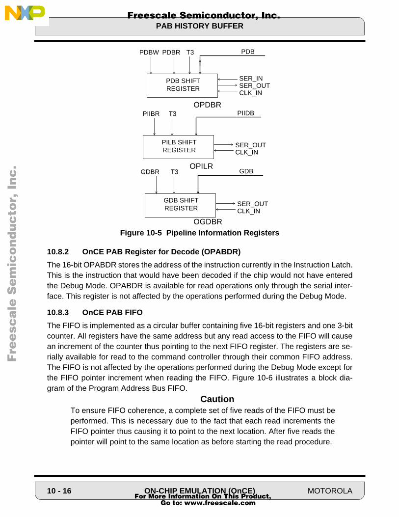
PAB HISTORY BUFFER
Fre
esc
ale
Se
mic
on
du
cto
r, I
Freescale Semiconductor, Inc.n
c..
.
10.8.2 OnCE PAB Register for Decode (OPABDR)
The 16-bit OPABDR stores the address of the instruction currently in the Instruction Latch.This is the instruction that would have been decoded if the chip would not have enteredthe Debug Mode. OPABDR is available for read operations only through the serial inter-face. This register is not affected by the operations performed during the Debug Mode.
10.8.3 OnCE PAB FIFO
The FIFO is implemented as a circular buffer containing five 16-bit registers and one 3-bitcounter. All registers have the same address but any read access to the FIFO will causean increment of the counter thus pointing to the next FIFO register. The registers are se-rially available for read to the command controller through their common FIFO address.The FIFO is not affected by the operations performed during the Debug Mode except forthe FIFO pointer increment when reading the FIFO. Figure 10-6 illustrates a block dia-gram of the Program Address Bus FIFO.
CautionTo ensure FIFO coherence, a complete set of five reads of the FIFO must beperformed. This is necessary due to the fact that each read increments theFIFO pointer thus causing it to point to the next location. After five reads thepointer will point to the same location as before starting the read procedure.
T3GDBR
SER_OUTCLK_IN
GDB SHIFT REGISTER
GDB
T3PDBW
SER_INSER_OUTCLK_IN
PDB SHIFT REGISTER
OPDBR
PDB
T3PIIBR
SER_OUTCLK_IN
PILB SHIFT REGISTER
OPILR
PIIDB
PDBR
OGDBRFigure 10-5 Pipeline Information Registers
10 - 16 ON-CHIP EMULATION (OnCE) MOTOROLA For More Information On This Product,
Go to: www.freescale.com

PAB HISTORY BUFFER
F
ree
sca
le S
em
ico
nd
uc
tor,
I
Freescale Semiconductor, Inc.n
c..
.
READ DECODE ADDRESS DECODE ADDRESS
(OPABDR)
PAB
CIRCBUFWR
CIRCBUFINC
PABREGISTER #0
PFSHRWPFSHRR
SER_OUTCLK_IN
PAB FIFOSHIFT REGISTER
CIRCBUFRD
PABREGISTER #1
PABREGISTER #2
PABREGISTER #3
PABREGISTER #4
CIRCBUFDEC
CIRCULARPOINTER DECODER
READ DECODE ADDRESS DSP FETCH ADDRESS
(OPABFR)
Figure 10-6 Program Address Bus FIFO
MOTOROLA ON-CHIP EMULATION (OnCE) 10 - 17 For More Information On This Product,
Go to: www.freescale.com

SERIAL PROTOCOL DESCRIPTION
F
ree
sca
le S
em
ico
nd
uc
tor,
I
Freescale Semiconductor, Inc.n
c..
.
10.9 SERIAL PROTOCOL DESCRIPTION
In order to permit an efficient means of communication between the command controllerand the DSP chip, the following protocol has been adopted. Before starting any debuggingactivity, the command controller has to wait for an acknowledge from the chip which in-forms the command controller that it has entered the Debug Mode. Note that in case of abreakpoint, trace or software DEBUG/DEBUGcc instruction, the acknowledge itself is theone that initiates the debug session. The command controller communicates with the chipby sending 8-bit commands that may be accompanied by 16-bit data. After sending acommand, the command processor starts waiting for the chip to acknowledge executionof the command. The command processor may send a new command only after the chiphas acknowledged execution of the previous command.
10.9.1 OnCE Commands
There are two type of commands: read commands (when the chip will deliver required da-ta) and write commands (when the chip will receive data and will write it in one of the onchip resources). The commands are 8 bits long and have the format shown in Figure 10-7.
10.9.1.1 OnCE Register Select (RS4-RS0) Bits 0-4
The Register Select bits define which register is source(destination) for the read(write) op-eration.
7 6 5 4 3 2 1 0
R/W GO EX RS4 RS3 RS2 RS1 RS0
Figure 10-7 OnCE Command Format
10 - 18 ON-CHIP EMULATION (OnCE) MOTOROLA For More Information On This Product,
Go to: www.freescale.com

SERIAL PROTOCOL DESCRIPTION
F
ree
sca
le S
em
ico
nd
uc
tor,
I
Freescale Semiconductor, Inc.n
c..
.
10.9.1.2 OnCE Exit Command (EX) Bit 5
Bit 5 in the OnCE command word is the exit command. To leave the OnCE mode and re-enter the normal operating mode, both the EX and GO bits must be asserted in the OnCEinput command register. There are three exit conditions:
1. If EX and GO are set, the chip will leave the Debug Mode, execute the DSPinstruction in the pipeline and then resume normal operation. If the registerselect bits are set to $1F (RS4-RS0 = 11111) then the last instruction (the in-struction in the PILB) is re-executed.
2. If EX is set without GO, then when the OnCE has finished writing the instruc-tion latch (PILB) register, the OnCE state machine will get another commandinstead of leaving the OnCE mode.
3. If EX is set without GO, then when the OnCE is finished writing the PDB(PILB) register, the OnCE state machine will get another command instead ofleaving the OnCE mode.
There is no acknowledgment on the DSO pin when the chip leaves the OnCE mode fol-lowing a GO or an EX.
RS4-RS0 Register Selected
00000 Debug Status/Control (OSCR)00001 Memory Breakpoint Counter (OMBC)00010 Reserved00011 Trace Counter (OTC)00100 Memory Breakpoint Address (OMBAR)00101 Reserved00110 Reserved00111 Reserved01000 Global Data Bus (Transfer) Register (OGDBR)01001 Program Data Bus (OPDBR) Register01010 Program Address Bus (OPABFR) Latch for Fetch01011 Instruction Latch (OPILR)01100 Clear Breakpoint Counter01101 Reserved01110 Clear Trace Counter01111 Reserved10000 Reserved10001 Program Address Bus FIFO and Increment Counter10010 Reserved10011 Program Address Bus (OPABDR) Latch for Decode101xx Reserved11xx0 Reserved11x0x Reserved110xx Reserved11111 No Register Selected
MOTOROLA ON-CHIP EMULATION (OnCE) 10 - 19 For More Information On This Product,
Go to: www.freescale.com
DSP56100 TARGET SITE DEBUG SYSTEM REQUIREMENTS
F
ree
sca
le S
em
ico
nd
uc
tor,
I
Freescale Semiconductor, Inc.n
c..
.
10.9.1.3 OnCE Go Command (GO) Bit 6
If GO is set, execute instruction. There is no acknowledgment on the DSO pin when thechip leaves the OnCE mode following a GO or an EX.
10.9.1.4 OnCE Read/Write Command (R/W) Bit 7
10.10 DSP56100 TARGET SITE DEBUG SYSTEM REQUIREMENTS
A typical debug environment consists of a target system where the DSP resides in theuser defined hardware. The debug serial port interfaces to the command convertor overa six wire link consisting of the four debug serial lines, a ground and reset wire. The resetwire is optional and is only used to reset the DSP and its associated circuitry.
The command controller acts as the medium between the DSP target system and a hostcomputer. The host computer interfaces to the controller using a standard RS232 threewire cable or the Application Development System parallel bus. A jumper option on thecommand controller board will select which method of communications will be used. Thisallows a variety of different host computers to communicate with the controller circuit. Thecontroller circuit provides several important functions. It acts as a serial debug port driver,host computer command interpreter, and DSP controller. The DSP acts as a slave whenin the debug mode and provides data only upon request. The controller issues commandsbased on the host computer inputs from a user interface program which communicateswith the user.
EX Action
0 Remain in Debug Mode1 Leave Debug Mode
GO Action
0 Inactive (no action taken)1 Execute DSP instruction
R/W Action
0 Write the data associated with the command into the register specified by RS4-RS01 Read the data contained in the register specified by RS4-RS0
10 - 20 ON-CHIP EMULATION (OnCE) MOTOROLA For More Information On This Product,
Go to: www.freescale.com

USING THE OnCE
F
ree
sca
le S
em
ico
nd
uc
tor,
I
Freescale Semiconductor, Inc.n
c..
.
10.11 USING THE OnCE
The following notations are used:
Commands require eight clocksACK = Wait for acknowledge on DSO line
CLK = Issue 16 clocks to read out data from selected register
10.11.1 Begin Debug Activity
Debug activity begins on an instruction boundary after the DR pin is asserted, a DEBUGccopcode is executed, a trace countdown occurs, or a breakpoint register countdown oc-curs. If the instruction executing when the DR pin is asserted is a REP instruction or theinstruction following a REP instruction, then the debug activity will begin after the instruc-tion following the REP instruction finishes being repeated. The first ACK indicates that theOnCE controller is ready to receive commands and data. Most of the Debug activities willhave the following beginning:
ACK
1. Save pipeline information:a. Send command READ PDB REGISTERb. ACKc. CLKd. Send command READ OPILRe. ACKf. CLK
2. Read PAB FIFO and fetch/decode info (this step is optional):a. Send command READ PAB address for fetchb. ACKc. CLKd. Send command READ PAB address for decodee. ACKf. CLKg. Send command READ FIFO REGISTER (and increment pointer)h. ACKi. CLKj. Send command READ FIFO REGISTER (and increment pointer)k. ACKl. CLK
MOTOROLA ON-CHIP EMULATION (OnCE) 10 - 21 For More Information On This Product,
Go to: www.freescale.com

USING THE OnCE
F
ree
sca
le S
em
ico
nd
uc
tor,
I
Freescale Semiconductor, Inc.n
c..
.
m. Send command READ FIFO REGISTER (and increment pointer)n. ACKo. CLKp. Send command READ FIFO REGISTER (and increment pointer)q. ACKr. CLKs. Send command READ FIFO REGISTER (and increment pointer)t. ACKu. CLK
10.11.2 Displaying a Specified Register
1. Send command WRITE PDB REGISTER and GO (no EX)(ODEC selects PDB as destination for serial data.)
2. ACK
3. Send the 16-bit opcode: “MOVE reg, x:OGDB(After all 16-bits have been received, the PDB register drives the PDB. ODECgenerates PRNEW and releases the chip from the “halt” state and the contents ofthe register specified in the instruction is loaded in the GDB REGISTER. ThePRCYC1 signal (an internal signal) that marks the end of the instruction brings thechip again in the “halt” state and an acknowledge is issued to the commandcontroller)
4. ACK
5. Send command READ GDB REGISTER(ODEC selects GDB as the source for serial data and an acknowledge is issued tothe command controller)
6. ACK
7. CLK
10.11.3 Displaying X Memory Area Starting from Address xxxx
This command uses Rn to minimize serial traffic.
1. Send command WRITE PDB REGISTER and GO (no EX).(ODEC selects PDB as destination for serial data.)
2. ACK
10 - 22 ON-CHIP EMULATION (OnCE) MOTOROLA For More Information On This Product,
Go to: www.freescale.com

USING THE OnCE
F
ree
sca
le S
em
ico
nd
uc
tor,
I
Freescale Semiconductor, Inc.n
c..
.
3. Send the 16-bit opcode: “MOVE R0,x:OGDB”(After all 16-bits have been received, the PDB register drives the PDB. ODECgenerates PRNEW and releases the chip from the “halt” state and the contents ofR0 are loaded in the GDB REGISTER. The PRCYC1 signal that marks the end ofthe instruction brings the chip again to the “halt” state and an acknowledge isissued to the command controller)
4. ACK
5. Send command READ GDB REGISTER(ODEC selects GDB as the source for serial data and an acknowledge is issued tothe command controller)
6. ACK
7. CLK(The command controller generates 16 clocks that shift out the contents of theGDB register. The value of R0 is thus saved and will be restored before exiting theDebug Mode)
8. Send command WRITE PDB REGISTER (no GO, no EX).(ODEC selects PDB as destination for serial data.)
9. ACK
10.Send the 16-bits of opcode: “MOVE #$xxxx,R0” (After all 16-bits have been received, the PDB register drives the PDB. ODECgenerates PRNEW so the PILR is loaded with the opcode. An acknowledge isissued to the command controller)
11.ACK
12.Send command WRITE PDB REGISTER and GO (no EX). (ODEC selects PDB as destination for serial data.)
13.ACK
14.Send the 16-bits of the 2nd word of: “MOVE #$xxxx,R0” (the xxxx field) where xxxxis the address to be read.(After all 16-bits have been received, the PDB register drives the PDB. ODECreleases the chip from the “halt” state and the instruction starts execution. ThePRCYC1 signal that marks the end of the instruction brings the chip again to the“halt” state and an acknowledge is issued to the command controller)
MOTOROLA ON-CHIP EMULATION (OnCE) 10 - 23 For More Information On This Product,
Go to: www.freescale.com

USING THE OnCE
F
ree
sca
le S
em
ico
nd
uc
tor,
I
Freescale Semiconductor, Inc.n
c..
.
15.ACK
16.Send command WRITE PDB REGISTER and GO (no EX).(ODEC selects PDB as destination for serial data.)
17. ACK
18.Send the 16-bit opcode: “MOVE X:(R0)+,x:OGDB”(After all 16-bits have been received, the PDB register drives the PDB. ODECgenerates PRNEW and releases the chip form the “halt” state and the contents ofX:(R0) are loaded in the GDB REGISTER. The PRCYC1 signal that marks the endof the instruction brings the chip again in the “halt” state and an acknowledge isissued to the command controller)
19.ACK
20.Send command READ GDB REGISTER(ODEC selects GDB as source for serial data and an acknowledge is issued to thecommand controller)
21.ACK
22.CLK
23.Send command NO SELECTION and GO (no EX).(ODEC releases the chip from the “halt” state and the instruction is executed onceagain (in a “REPEAT-like” fashion. The PRCYC1 signal that marks the end of theinstruction brings the chip again to the “halt” state and an acknowledge is issuedto the command controller.)
24.ACK
25.Send command READ GDB REGISTER(ODEC selects GDB as source for serial data and an acknowledge is issued to thecommand controller.)
26.ACK
27.CLK
28.Repeat from step 23 until the entire memory area is examined. At the end of theprocess R0 has to be restored.
10 - 24 ON-CHIP EMULATION (OnCE) MOTOROLA For More Information On This Product,
Go to: www.freescale.com
USING THE OnCE
F
ree
sca
le S
em
ico
nd
uc
tor,
I
Freescale Semiconductor, Inc.n
c..
.
10.11.4 Returning from Debug Mode to Normal Mode
There are two cases for returning from the debug mode. In case 1, control will be returnedto the program that was running before debug was initiated and in case 2, the registerswill be changed to jump to a different program. There is no acknowledgment on the DSOpin when the chip leaves the OnCE mode following a GO, EX. This is a special case ofthe “write a register” option.
10.11.4.1 Case 1: Returning from Debug Mode to Normal Mode
1. Send command WRITE PDB REGISTER (no GO, no EX).
(ODEC selects the PDB register as destination for serial data. Also ODEC selectsthe on-chip PAB register as source for the PAB bus. After the PAB was driven anacknowledge is issued to the command controller)
2. ACK
3. Send the 16-bits of the saved PILB (instruction latch) value.
(After all 16-bits have been received, the PDB register drives the PDB. ODECgenerates PRNEW so the entire chip loads the opcode. An acknowledge is issuedto the command controller)
4. ACK
5. Send command WRITE PDB REGISTER (GO, EX).(ODEC selects PDB as destination for serial data.)
6. ACK
7. Send the 16-bits of the saved PDB value. (After all 16-bits have been received, the PDB register drives the PDB. ODECreleases the chip form the “halt” state and the Debug Mode bit in OSCR is cleared.The chip continues to execute instructions until a Debug Mode condition occurs)
10.11.4.2 Case 2: Jump to a New Program (Go from Address $xxxx).
1. Send command WRITE PDB REGISTER (no GO, no EX).(ODEC selects PDB as destination for serial data.)
2. ACK
MOTOROLA ON-CHIP EMULATION (OnCE) 10 - 25 For More Information On This Product,
Go to: www.freescale.com
USING THE OnCE
F
ree
sca
le S
em
ico
nd
uc
tor,
I
Freescale Semiconductor, Inc.n
c..
.
3. Send 16 bits of the opcode of a two word jump instruction instead of the saved PIL(instruction latch) value.
(After all the 16-bits have been received, the PDB register drives the PDB. ODECcauses the DSP to load the opcode. An acknowledge is issued to the commandcontroller.)
4. ACK
5. Send command WRITE PDB REGISTER (GO, EX).(ODEC selects PDB as destination for serial data.)
6. ACK
7. Send 16 bits of the target absolute address ($xxxx). The chip will resume fetchingfrom the target address (you do not have to worry about the pipeline). Note that thetrace counter will count this instruction so the current trace counter may need to becorrected if the trace mode enable bit in the OSCR has been set.
(e. g., After 16 bits have been received, the PDB register drives the PDB. ODECreleases the chip from the “halt” state and the Debug Mode bit in OSCR is cleared.The chip executes first the jump instruction and will then fetch the instruction fromthe target address. The chip continues to execute instructions from that addressuntil a Debug Mode condition occurs.)
10 - 26 ON-CHIP EMULATION (OnCE) MOTOROLA For More Information On This Product,
Go to: www.freescale.com

Fre
esc
ale
Se
mic
on
du
cto
r, I
Freescale Semiconductor, Inc.n
c..
.
SECTION 11
APPLICATION DEVELOPMENT TOOLS
MOTOROLA APPLICATION DEVELOPMENT TOOLS 11 - 1 For More Information On This Product,
Go to: www.freescale.com

SECTION CONTENTS
Fre
esc
ale
Se
mic
on
du
cto
r, I
Freescale Semiconductor, Inc.n
c..
.
11.1 SOFTWARE . . . . . . . . . . . . . . . . . . . . . . . . . . . . . . . . . . . . . . . . . . . . 11-311.2 MACRO CROSS ASSEMBLER . . . . . . . . . . . . . . . . . . . . . . . . . . . . . 11-311.3 LINKER/LIBRARIAN . . . . . . . . . . . . . . . . . . . . . . . . . . . . . . . . . . . . . . 11-411.4 SIMULATOR PROGRAM . . . . . . . . . . . . . . . . . . . . . . . . . . . . . . . . . . 11-411.5 HARDWARE . . . . . . . . . . . . . . . . . . . . . . . . . . . . . . . . . . . . . . . . . . . . 11-511.6 HARDWARE FEATURES . . . . . . . . . . . . . . . . . . . . . . . . . . . . . . . . . . 11-711.7 SOFTWARE FEATURES . . . . . . . . . . . . . . . . . . . . . . . . . . . . . . . . . . 11-811.8 OPERATING ENVIRONMENT . . . . . . . . . . . . . . . . . . . . . . . . . . . . . . 11-8
11 - 2 APPLICATION DEVELOPMENT TOOLS MOTOROLA For More Information On This Product,
Go to: www.freescale.com

SOFTWARE
Fre
esc
ale
Se
mic
on
du
cto
r, I
Freescale Semiconductor, Inc.n
c..
.
11.1 SOFTWAREAll software support products run on the following platforms — IBM PC, Macintosh ,and SUN workstation. The software, written in C, consists of an assembler, linker, andsimulator which are marketed as an integrated product.
11.2 MACRO CROSS ASSEMBLERThe ASM56100 Macro Cross Assembler program is a full-featured macro cross assem-bler that translates one or more source fields containing DSP instruction mnemonics,operands, and assembler directives into relocatable object modules that are relocatedand linked by the Motorola DSP Linker in the Relocation mode. In the Absolute mode,the assembler will generate absolute executable files. The assembler recognizes the fullinstruction set and all addressing modes of the DSP56100 family.
This assembler offers the usual complement of features found in modern assemblers,such as conditional assembly, file inclusion, nested macros with support for macro librar-ies (via the MACLIB directive), and modular programming constructs ordinarily foundonly in higher level languages.
The unique architecture and parallel operation of the DSP demands special purposefacilities and programming aids which this assembler readily provides. These includebuilt-in functions for common transcendental math computations such as sine, cosine,log, and square root functions; arbitrary expressions and modulo operations; and direc-tives to define circular and bit-reversed data buffers. Moreover, the assembler incorpo-rates extensive error checking and reporting to indicate programming violations peculiarto the digital signal processing environment or stemming from the advanced features ofthe DSP. These include errors for improper nesting of hardware DO loops and improperaddress boundaries for circular data buffers and bit-reversed buffers.
The assembler also generates source code listings which include numbered sourcelines, optional titles and subtitles, optional instruction cycle counts, symbol table andcross-reference listings, and memory use reports.
To summarize, features of the assembler are:
• Produces relocatable object modules compatible with the DSP linker program in the Relocation mode
• Produces absolute executable files compatible with the Simulator program (SIM56100) in the Absolute mode
• Supports full instruction set, memory spaces, and parallel data transfer fields of the DSP
• Modular programming features including local labels, sections, and external definition/reference directives
MOTOROLA APPLICATION DEVELOPMENT TOOLS 11 - 3 For More Information On This Product,
Go to: www.freescale.com
LINKER/LIBRARIAN
Fre
esc
ale
Se
mic
on
du
cto
r, I
Freescale Semiconductor, Inc.n
c..
.
• Nested macro libraries• Complex expression evaluation including boolean operators• Built-in functions for data conversion, string comparison, and common transcendental
math operations• Directives to define circular and bit-reversed buffers• Extensive error checking and reporting
11.3 LINKER/LIBRARIANThe linker relocates and links relocatable object modules from the Macro Cross Assem-bler to create an absolute executable file which can be loaded directly into theDSP56100 simulator or converted to Motorola S-record format for PROM burning.
The librarian utility will merge into a single file multiple separate relocatable object mod-ules. This facilitates not having to reassemble known bug-free routines every time themainline program is assembled.
11.4 SIMULATOR PROGRAMThe SIM56100 Simulator program is a software tool for developing programs and algo-rithms for the DSP. This program exactly emulates all of the functions (except for theOnCE) of the DSP including all on-chip peripheral operations, the entire internal andexternal memory space, all memory and register updates associated with program codeexecution, and all exception processing activity. This enables the Simulator program toprovide an accurate measurement of code execution time which is so critical in digitalsignal processing applications.
The Simulator program executes DSP object code generated by the Linker or the Simu-lator’s internal single-line assembler. The object code is loaded into the simulated DSPmemory map. Instruction execution can proceed until a user-defined breakpoint isencountered; or in single-step mode, stopping after each instruction has been executed.During program debug, the registers or memory locations may be displayed or changed.
The Simulator package includes linkable object code libraries of simulator functions thatwere used to create the simulator. The libraries allow a customized simulator to be builtand integrated with unique system simulations. Source code for some of the functions,such as the terminal I/O functions and external memory accesses, is provided to allowclose simulation of the particular application.
To summarize, features of the Simulator program are:
Summary of simulator features:• Multiple device simulation
11 - 4 APPLICATION DEVELOPMENT TOOLS MOTOROLA For More Information On This Product,
Go to: www.freescale.com

HARDWARE
Fre
esc
ale
Se
mic
on
du
cto
r, I
Freescale Semiconductor, Inc.n
c..
.
• Source level symbolic debug of assembly source programs• Conditional or unconditional breakpoints• Program patching using a Single-Line Assembler/Disassembler• Instruction and Cycle timing counters• Session and/or Command Logging for later reference• Input/Output ASCII files for device peripherals• Help file and Help line display of Simulator commands• Macro command definition and execution• Display Enable/Disable of Registers and Memory• Hexadecimal/Decimal/Binary calculator
11.5 HARDWAREEach DSP56100 family member has an Application Development System (ADS). All ofthese are essentially identical in operation and features. The differences that do exist aredue to the specific nature of each chip. While the example here is the DSP56156, allDSP56100 family ADS’s operate in essentially the same way. Upgrading an ADS to runa different Motorola DSP is done by purchasing and plugging in a new Application Devel-opment Module (see Figure 11-1).
The DSP56156 ADS is a four component system which acts as a development tool fordesigning, debugging, and evaluating real-time DSP56156 target system equipment.The ADS simplifies evaluation of the user’s prototype hardware/software product bymaking all of the essential DSP56156 timing and I/O circuitry easily accessible. The ADStakes full advantage of the On-Chip Emulation (OnCE) circuits of the DSP to allow theuser to control the target non-intrusively.
An IBM PC, Macintosh II, or SUN acts as the medium between the user and the DSPhardware. The four components consist of an Application Development Module (ADM)which contains a DSP56156 processor and control circuitry, a HOST-BUS interfaceboard for controlling up to 8 ADMs, a command convertor board which interacts with thetarget OnCE serial debug port, and a software program which interacts with the user andcontrols the ADM(s) and/or target system.
DSP algorithm development is simplified with features such as multiple file I/O capabilityto the target under DSP56156 program control and immediate access to a hex/fractionalarithmetic calculator. The ADS is fully compatible with the DSP56100CLASx design-insoftware package and may act as an accelerator for testing DSP56156 algorithms.DSP56156 programs may be executed in real-time or by single/multiple stepping throughinstructions.
MOTOROLA APPLICATION DEVELOPMENT TOOLS 11 - 5 For More Information On This Product,
Go to: www.freescale.com

HARDWARE
Fre
esc
ale
Se
mic
on
du
cto
r, I
Freescale Semiconductor, Inc.n
c..
.
As many as 99 conditional and/or unconditional software breakpoints may be placed inADM program memory. A hardware breakpoint range may be set to halt program execu-tion whenever a program or data address falls within the specified range. All breakpointsmay have actions associated with them or may cause an immediate halt and display ofenabled registers.
Figure 11-1 illustrates the ADS being used as a hardware evaluation tool or softwareaccelerator. The ADM card has a 10 pin connector which provides an access point forthe command convertor OnCE interface.
Figure 11-2 illustrates the ADS being used as an emulator where the user has a defined
User Application CircuitsDSP5615637 pin
Host ComputerInterface Card
(Host Computer)IBM PC,MacintoshSun 3
OnCE Command Convertor
Application Development Module (ADM)
InterfaceCable
Host ComputerInterface Card OnCE Command Convertor
DSP56156OnCESerialInterface
Target DSP56156System(Host Computer)
IBM PC,MacintoshSun
37 pinInterfaceCable
Figure 11-1 Application Development
Figure 11-2 Target Circuit Emulation
11 - 6 APPLICATION DEVELOPMENT TOOLS MOTOROLA For More Information On This Product,
Go to: www.freescale.com
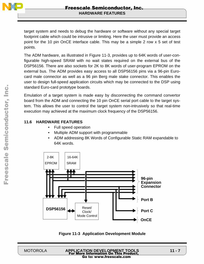
HARDWARE FEATURES
Fre
esc
ale
Se
mic
on
du
cto
r, I
Freescale Semiconductor, Inc.n
c..
.
target system and needs to debug the hardware or software without any special targetfootprint cable which could be intrusive or limiting. Here the user must provide an accesspoint for the 10 pin OnCE interface cable. This may be a simple 2 row x 5 set of testpoints.
The ADM hardware, as illustrated in Figure 11-3, provides up to 64K words of user-con-figurable high-speed SRAM with no wait states required on the external bus of theDSP56156. There are also sockets for 2K to 8K words of user-program EPROM on theexternal bus. The ADM provides easy access to all DSP56156 pins via a 96-pin Euro-card male connector as well as a 96 pin Berg male stake connector. This enables theuser to design full-speed application circuits which may be connected to the DSP usingstandard Euro-card prototype boards.
Emulation of a target system is made easy by disconnecting the command convertorboard from the ADM and connecting the 10 pin OnCE serial port cable to the target sys-tem. This allows the user to control the target system non-intrusively so that real-timeexecution may achieved at the maximum clock frequency of the DSP56156.
11.6 HARDWARE FEATURES• Full speed operation• Multiple ADM support with programmable • ADM addressing 8K Words of Configurable Static RAM expandable to
64K words.
DSP56156 Reset/Clock/
Mode Control
2-8K
EPROM
16-64K
SRAM
96-pinExpansionConnector
Port B
Port C
OnCE
Figure 11-3 Application Development Module
MOTOROLA APPLICATION DEVELOPMENT TOOLS 11 - 7 For More Information On This Product,
Go to: www.freescale.com

SOFTWARE FEATURES
Fre
esc
ale
Se
mic
on
du
cto
r, I
Freescale Semiconductor, Inc.n
c..
.
• 2K Words of EPROM with sockets expandable to 64K words.• Stand-Alone operation of ADM after initial development.• Full support of program/data memory maps.• 96 pin Connector provides access to all DSP56156 pins.• OnCE Command Convertor card for non-intrusive Real Time Emulation.• Special peripheral connectors available for easy access to DSP
peripherals.• 3V emulation support in target environments
11.7 SOFTWARE FEATURES• Single/Multiple stepping through DSP56156 object programs.• Conditional or unconditional software and hardware breakpoints.• Program patching using a Single-Line Assembler/Disassembler.• Session and/or Command Logging for later reference.• Loading and Saving of files to/from ADM Memory.• Macro command definition and execution.• Display Enable/Disable of Registers and Memory.• Debug commands which support Multiple DSP56156 development.• Hexadecimal/Decimal/Binary Fractional calculator.• System commands from within ADS User Interface Program.• Multiple Input/Output file access from DSP56156 object programs.• On-line help screens for each command and DSP56156 register.• Compatible with the DSP56100CLASX Assembler and Simulator
11.8 OPERATING ENVIRONMENTThe minimum hardware requirements for the DSP56156ADS User Interface Programinclude: IBM PC-DOS/MS-DOS v3.x, 4.x, or 5.x; Macintosh II with 1 Mbyte of RAM andrunning Mac OS 4.2 or later; or SUN-4 running BSD 4.2 with SUNOS 4.1.2 or Solaris 2.x.
11 - 8 APPLICATION DEVELOPMENT TOOLS MOTOROLA For More Information On This Product,
Go to: www.freescale.com
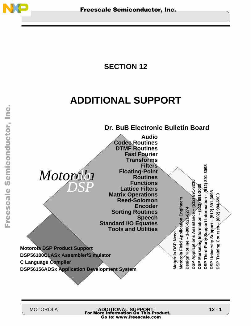
MoDSC LDS
Fre
esc
ale
Se
mic
on
du
cto
r, I
Freescale Semiconductor, Inc.n
c..
.
SECTION 12
ADDITIONAL SUPPORT
Dr. BuB Electronic Bulletin BoardAudio
Codec RoutinesDTMF Routines
Fast FourierTransforms
FiltersFloating-Point
RoutinesFunctions
Lattice FiltersMatrix Operations
Reed-SolomonEncoder
Sorting RoutinesSpeech
Standard I/O EquatesTools and Utilities
Mo
toro
la D
SP
New
s
Mo
toro
la F
ield
Ap
plic
atio
n E
ng
inee
rs
Des
ign
Ho
tlin
e –
1-80
0-52
1-62
74
DS
P A
pp
licat
ion
s A
ssis
tan
ce –
(51
2) 8
91-3
230
DS
P M
arke
tin
g In
form
atio
n –
(51
2) 8
91-2
030
DS
P T
hir
d-P
arty
Su
pp
ort
Info
rmat
ion
– (
512)
891
-309
8
DS
P U
niv
ersi
ty S
up
po
rt –
(51
2) 8
91-3
098
DS
P T
rain
ing
Co
urs
es –
(60
2) 9
94-6
900
torola DSP Product SupportP56100CLASx Assembler/Simulatoranguage CompilerP56156ADSx Application Development System
MotorolaDSPola
MOTOROLA For
ADDITIONAL SUPPORT 12 - 1More Information On This Product,
Go to: www.freescale.com

SECTION CONTENTS
Fre
esc
ale
Se
mic
on
du
cto
r, I
Freescale Semiconductor, Inc.n
c..
.
12.1 INTRODUCTION . . . . . . . . . . . . . . . . . . . . . . . . . . . . . . . . . . . . . . . . 12-312.2 THIRD PARTY SUPPORT . . . . . . . . . . . . . . . . . . . . . . . . . . . . . . . . . 12-312.3 MOTOROLA DSP PRODUCT SUPPORT . . . . . . . . . . . . . . . . . . . . . 12-412.4 SUPPORT INTEGRATED CIRCUITS . . . . . . . . . . . . . . . . . . . . . . . . 12-612.5 MOTOROLA DSP NEWS . . . . . . . . . . . . . . . . . . . . . . . . . . . . . . . . . . 12-712.6 MOTOROLA FIELD APPLICATION ENGINEERS . . . . . . . . . . . . . . . 12-712.7 DSP APPLICATIONS HELP LINE – (512) 891-3230 . . . . . . . . . . . . . 12-712.8 DESIGN HOTLINE – 1-800-521-6274 . . . . . . . . . . . . . . . . . . . . . . . . 12-712.9 DSP MARKETING INFORMATION – (512) 891-2030 . . . . . . . . . . . . 12-712.10 DSP THIRD-PARTY SUPPORT INFORMATION – (512) 891-3098 . 12-712.11 DSP UNIVERSITY SUPPORT – (512) 891-3098 . . . . . . . . . . . . . . . . 12-712.12 DSP TRAINING COURSES – (602) 897-3665 or (800) 521-6274 . . . 12-812.13 Dr. BuB ELECTRONIC BULLETIN BOARD . . . . . . . . . . . . . . . . . . . . 12-812.14 REFERENCE BOOKS AND MANUALS . . . . . . . . . . . . . . . . . . . . . . . 12-18
12 - 2 ADDITIONAL SUPPORT MOTOROLA For More Information On This Product,
Go to: www.freescale.com

INTRODUCTION
Fre
esc
ale
Se
mic
on
du
cto
r, I
Freescale Semiconductor, Inc.n
c..
.
12.1 INTRODUCTIONThis section is intended as a guide to the DSP support services and products offered byMotorola. This includes training, development hardware and software tools, telephonesupport, etc.
12.2 THIRD PARTY SUPPORTUser support from the conception of a design through completion is available from Motor-ola and third-party companies as shown in the following list:
Motorola Third Party
Design Data Sheets Data Acquisition PackagesApplication Notes Filter Design PackagesApplication Bulletins Operating System SoftwareSoftware Examples Simulator
Prototyping Assembler Logic Analyzer withLinker DSP561xx ROM PackagesC Compiler Data Acquisition CardsSimulator DSP Development SystemApplication Development Cards
System (ADS) Operating System SoftwareIn-Circuit Emulator Debug Software
Cable for ADS
Design Application Development Data Acquisition PackagesVerification System (ADS) Logic Analyzer with
In-Circuit Emulator DSP561xx ROM PackagesSimulator Data Acquisition Cards
DSP Development SystemCards
Application-SpecificDevelopment Tools
Debug Software
Specific information on the companies that offer these products is available by calling theDSP third party information number given in Section 12.10.
MOTOROLA ADDITIONAL SUPPORT 12 - 3 For More Information On This Product,
Go to: www.freescale.com

MOTOROLA DSP PRODUCT SUPPORT
Fre
esc
ale
Se
mic
on
du
cto
r, I
Freescale Semiconductor, Inc.n
c..
.
The following is a partial list of the support available for the DSP561xx. Additionalinformation on DSP56100 family members can be obtained through Dr. BuB or theappropriate support telephone service.
12.3 MOTOROLA DSP PRODUCT SUPPORT• DSP56100CLASx Design-In Software Package which includes:
Relocatable Macro Assembler
Linker
Simulator (simulates single or multiple DSP561xxs)
Librarian
• DSP561xx Applications Development System (ADS)
• Support Integrated Circuits
• DSP Bulletin Board (Dr. BuB)
• Motorola DSP Newsletter
• Motorola Technical Service Engineers (TSEs)See your local telephone directory for the Motorola Semiconductor Sector sales office telephone number.
• Design Hotline
• Applications Assistance
• Marketing Information
• Third-Party Support Information
• University Support Information
12.3.1 DSP56100CLASx Assembler/Simulator
12.3.1.1 Macro Cross Assembler and Simulator Platforms1. IBM PCs and clones using an 80386 or upward compatible processor
2. Macintosh computers with a NU-BUS expansion port
3. SUN computer
12.3.1.2 Macro Cross Assembler Features• Production of relocatable object modules compatible with linker program when in
relocatable mode
• Production of absolute files compatible with simulator program when in absolute mode
• Supports full instruction set, memory spaces, and parallel data transfer fields of the DSP561xx
12 - 4 ADDITIONAL SUPPORT MOTOROLA For More Information On This Product,
Go to: www.freescale.com

MOTOROLA DSP PRODUCT SUPPORT
Fre
esc
ale
Se
mic
on
du
cto
r, I
Freescale Semiconductor, Inc.n
c..
.
• Modular programming features: local labels, sections, and external definition/ref-erence directives
• Nested macro processing capability with support for macro libraries
• Complex expression evaluation including boolean operators
• Built-in functions for data conversion, string comparison, and common transcen-dental math functions
• Directives to define circular and bit-reversed buffers
• Extensive error checking and reporting
12.3.1.3 Simulator Features• Simulation of all DSP56100 family DSPs
• Simulation of multiple DSP56100 family DSPs
• Linkable object code modules:
–Nondisplay simulator library
–Display simulator library
• C language source code for:
–Screen management functions
–Terminal I/O functions
–Simulation examples
• Single stepping through object programs
• Conditional or unconditional breakpoints
• Program patching using a single-line assembler/disassembler
• Instruction, clock cycle, and histogram counters
• Session and/or command logging for later reference
• ASCII input/output files for peripherals
• Help-line display and expanded on-line help for simulator commands
• Loading and saving of files to/from simulator memory
• Macro command definition and execution
• Display enable/disable of registers and memory
• Hexadecimal/decimal/binary calculator
12.3.2 Application Development Systems• Application Development Systems (ADS) are available for all family members. Up-
grading an ADS to run a different Motorola DSP is done by purchasing and plug-ging in a new Application Development Module.
MOTOROLA ADDITIONAL SUPPORT 12 - 5 For More Information On This Product,
Go to: www.freescale.com

SUPPORT INTEGRATED CIRCUITS
Fre
esc
ale
Se
mic
on
du
cto
r, I
Freescale Semiconductor, Inc.n
c..
.
12.3.2.1 DSP561xxADSx Application Development System Hardware Features• Full-speed operation
• Multiple application development module (ADM) support with programmable ADM addresses
• User-configurable RAM for DSP561xx code development
• Expandable monitor ROM
• 96-pin Euro-card connector making all pins accessible
• In-circuit emulation capabilities using OnCE
• Separate berg pin connectors for alternate accessing of serial or host/DMA ports
• ADM can be used in stand-alone configuration
• No external power supply needed when connected to a host platform
• 3V emulation support in target environments
12.3.2.2 DSP561xxADSx Application Development System Software Features• Full-speed operation
• Single/multiple stepping through DSP561xx object programs
• Up to 99 conditional or unconditional breakpoints
• Program patching using a single-line assembler/disassembler
• Session and/or command logging for later reference
• Loading and saving files to/from ADM memory
• Macro command definition and execution
• Display enable/disable of registers and memory
• Debug commands supporting multiple ADMs
• Hexadecimal/decimal/binary calculator
• Host operating system commands from within ADS user interface program
• Multiple OS I/O file access from DSP561xx object programs
• Fully compatible with the DSP56100CLASx design-in software package
• On-line help screens for each command and DSP561xx register
12.4 SUPPORT INTEGRATED CIRCUITS• DSP56ADC16 16-bit, 100-kHz analog-to-digital converter
• DSP56401 AES/EBU processor
• DSP56200 FIR filter
12 - 6 ADDITIONAL SUPPORT MOTOROLA For More Information On This Product,
Go to: www.freescale.com
MOTOROLA DSP NEWS
Fre
esc
ale
Se
mic
on
du
cto
r, I
Freescale Semiconductor, Inc.n
c..
.
12.5 MOTOROLA DSP NEWSThe Motorola DSP News is a quarterly newsletter providing information on new products,application briefs, questions and answers, DSP product information, third-party productnews, etc. This newsletter is free and is available upon request by calling the marketinginformation phone number listed below.
12.6 MOTOROLA FIELD APPLICATION ENGINEERSInformation and assistance for DSP applications is available through the local Motorolafield office. See your local telephone directory for telephone numbers or call (512)891-2030.
12.7 DSP APPLICATIONS HELP LINE – (512) 891-3230Design assistance for specific DSP applications is available by calling this number.
12.8 DESIGN HOTLINE – 1-800-521-6274This is the Motorola number for information pertaining to any Motorola product.
12.9 DSP MARKETING INFORMATION – (512) 891-2030Marketing information including brochures, application notes, manuals, price quotes, etc.for Motorola DSP-related products are available by calling this number.
12.10 DSP THIRD-PARTY SUPPORT INFORMATION – (512) 891-3098Information concerning third-party manufacturers using and supporting Motorola DSPproducts is available by calling this number. Third-party support includes:
Filter design software
Logic analyzer support
Boards for VME, IBM-PC/XT/AT, MACII, SPARC, HP300
Development systems
Data conversion cards
Operating system software
Debug software
Additional information is available on Dr. BuB and in DSP News.
12.11 DSP UNIVERSITY SUPPORT – (512) 891-3098Information concerning university support programs and university discounts for allMotorola DSP products is available by calling this number.
MOTOROLA ADDITIONAL SUPPORT 12 - 7 For More Information On This Product,
Go to: www.freescale.com

DSP TRAINING COURSES – (602) 897-3665 or (800) 521-6274
Fre
esc
ale
Se
mic
on
du
cto
r, I
Freescale Semiconductor, Inc.n
c..
.
12.12 DSP TRAINING COURSES – (602) 897-3665 or (800) 521-6274Training information on the DSP56100 family members is available by writing:
Motorola SPS Training and Technical Operations
Mail Drop EL524
P. O. Box 21007
Phoenix, Arizona 85036
or by calling the number above. A technical training catalog is available which describesthese courses and gives the current training schedule and prices.
12.13 Dr. BuB ELECTRONIC BULLETIN BOARDDr. BuB is an electronic bulletin board providing free source code for a large variety oftopics that can be used to develop applications with Motorola DSP products. The softwarelibrary includes files including FFTs, FIR filters, IIR filters, lattice filters, matrix algebraroutines, companding routines, floating-point routines, and others. In addition, the latestproduct information and documentation (including information on new products andimprovements on existing products) is posted. Questions concerning Motorola DSPproducts posted on Dr. BuB are answered promptly.
Dr. BuB is open 24-hour a day, 7 days per week and offers the DSP community informa-tion on Motorola’s DSP products, including:
• Public domain source code for Motorola’s DSP products including the DSP56000 family, the DSP56100 family and the DSP96002
• Announcements about new products and policies• Technical discussion groups monitored by DSP application engineers• Confidential mail service• Calendar of events for Motorola DSP• Complete list of Motorola DSP literature and ordering information• Information about the Third-Party and University Support Programs.
To logon to the bulletin board, follow these instructions:
1. Set the character format on your modem to 8 data bits, no parity, 1 stop bit,then dial (512) 891-3771. Dr. BuB will automatically set the data transfer rateto match your modem (9600, 4800, 2400, 1200 or 300 BPS).
2. Once the connection has been established, you will see the Dr. BuB loginprompt (you may have to press the carriage return a couple times). If you justwant to browse the system, login as guest. If you would like all the privilegesthat are normally allowed on the system, enter new at the login prompt.
12 - 8 ADDITIONAL SUPPORT MOTOROLA For More Information On This Product,
Go to: www.freescale.com
Dr. BuB ELECTRONIC BULLETIN BOARD
Fre
esc
ale
Se
mic
on
du
cto
r, I
Freescale Semiconductor, Inc.n
c..
.
3. If you open a new account, you will be asked to answer some questions suchas name, address, phone number, etc. After answering these questions, youwill have immediate access to all features of the system including downloadprivilege, electronic mail and participation in discussion groups.
4. You will have an hour of access time for each call (upload and download timedoesn’t count against you) and you can call as often as you like. If you needmore time on line, just send an electronic mail request to the system operator(sysop).
The following is a partial list of the software available on Dr. BuB.
12.13.1 Audiorvb1.asm 1.0 Easy-to-read reverberation routine 17056
rvb2.asm 1.0 Same as RVB1.ASM but optimized 15442
stereo.asm 1.0 Code for C-QUAM AM stereo decoder 4830
stereo.hlp 1.0 Help file for STEREO.ASM 620
dge.asm 1.0 Digital Graphic Equalizer code from 14880
12.13.2 BenchmarksAppendix B.1 through B.2.26 DSP56116 (DSP56100 Family) Benchmarks 44436
Appendix B.3 through B.3.9 DSP56116 (DSP56100 Family) Benchmarks 6329
12.13.3 Codec Routinesloglin.asm 1.0 Companded CODEC to linear PCM data 4572
conversion
loglin.hlp Help for loglin.asm 1479
loglint.asm 1.0 Test program for loglin.asm 2184
loglint.hlp Help for loglint.asm 1993
linlog.asm 1.1 Linear PCM to companded CODEC data 4847conversion
linlog.hlp Help for linlog.asm 1714
12.13.4 DTMF Routinesclear.cmd 1.0 Explained in read.me file 119
data.lod 1.0 421
det.asm 1.0 Subroutine used in IIR DTMF 5923
Document ID Version Synopsis Size
MOTOROLA ADDITIONAL SUPPORT 12 - 9 For More Information On This Product,
Go to: www.freescale.com

Dr. BuB ELECTRONIC BULLETIN BOARD
Fre
esc
ale
Se
mic
on
du
cto
r, I
Freescale Semiconductor, Inc.n
c..
.
dtmf.asm 1.0 Main routine used in IIR DTMF 10685
dtmf.mem 1.0 Memory for DTMF routine 48
dtmfmstr.asm 1.0 Main routine for multichannel DTMF 7409
dtmfmstr.mem 1.0 Memory for multichannel DTMF routine 41
dtmftwo.asm 1.0 10256
ex56.bat 1.0 94
genxd.lod 1.0 Data file 183
genyd.lod 1.0 Data file 180
goertzel.asm 1.0 Goertzel routine 4393
goertzel.lnk 1.0 Link file for Goertzel routine 6954
goertzel.lst 1.0 List file for Goertzel routine 11600
load.cmd 1.0 46
tstgoert.mem 1.0 Memory for Goertzel routine 384
sub.asm 1.0 Subroutine linked for use in IIR DTMF 2491
read.me 1.0 Instructions 738
12.13.5 Fast Fourier Transformssincos.asm 1.2 Sine-Cosine Table Generator for FFTs 1185
sincos.hlp Help for sincos.asm 887
sinewave.asm 1.1 Full-Cycle Sine wave Table Generator 1029Generator Macro
sinewave.hlp for sinewave.asm 1395
fftr2a.asm 1.1 Radix 2, In-Place, DIT FFT (smallest) 3386
fftr2a.hlp Help for fftr2a.asm 2693
fftr2at.asm 1.1 Test Program for FFTs (fftr2a.asm) 999
fftr2at.hlp Help for fftr2at.asm 563
fftr2b.asm 1.1 Radix 2, In-Place, DIT FFT (faster) 4290
fftr2b.hlp Help for fftr2b.asm 3680
fftr2c.asm 1.2 Radix 2, In-Place, DIT FFT (even faster) 5991
fftr2c.hlp Help for fftr2c.asm 3231
fftr2d.asm 1.0 Radix 2, In-Place, DIT FFT (using 3727DSP56001 sine-cosine ROM tables)
fftr2d.hlp Help for fftr2d.asm 3457
Document ID Version Synopsis Size
12 - 10 ADDITIONAL SUPPORT MOTOROLA For More Information On This Product,
Go to: www.freescale.com
Dr. BuB ELECTRONIC BULLETIN BOARD
Fre
esc
ale
Se
mic
on
du
cto
r, I
Freescale Semiconductor, Inc.n
c..
.
fftr2dt.asm 1.0 Test program for fftr2d.asm 1287
fftr2dt.hlp Help for fftr2dt.asm 614
fftr2e.asm 1.0 1024 Point, Non-In-Place, FFT (3.39ms) 8976
fftr2e.hlp Help for fftr2e.asm 5011
fftr2et.asm 1.0 Test program for fftr2e.asm 984
fftr2et.hlp Help for fftr2et.asm 408
dct1.asm 1.1 Discrete Cosine Transform using FFT 5493
dct1.hlp 1.1 Help file for dct1.asm 970
fftr2cc.asm 1.0 Radix 2, In-place Decimation-in-time 6524complex FFT macro
fftr2cc.hlp 1.0 Help file for fftr2cc.asm 3533
fftr2cn.asm 1.0 Radix 2, Decimation-in-time Complex FFT 6584macro with normally ordered input/output
fftr2cn.hlp 1.0 Help file for fftr2cn.asm 2468
fftr2en.asm 1.0 1024 point, not-in-place, complex FFT 9723macro with normally ordered input/output
fftr2en.hlp 1.0 Help file for fftr2en.asm 4886
dhit1.asm 1.0 Routine to compute Hilbert transform 1851in the frequency domain
dhit1.hlp 1.0 Help file for dhit1.asm 1007
fftr2bf.asm 1.0 Radix-2, decimation-in-time FFT with 13526block floating point
fftr2bf.hlp 1.0 Help file for fftr2bf.asm 1578
fftr2aa.asm 1.0 FFT program for automatic scaling 3172
12.13.6 Filtersfir.asm 1.0 Direct Form FIR Filter 545
fir.hlp Help for fir.asm 2161
firt.asm 1.0 Test program for fir.asm 1164
iir1.asm 1.0 Direct Form Second Order All Pole 656IIR Filter
iir1.hlp Help for iir1.asm 1786
iir1t.asm 1.0 Test program for iir1.asm 1157
iir2.asm 1.0 Direct Form Second Order All Pole 801IIR Filter with Scaling
Document ID Version Synopsis Size
MOTOROLA ADDITIONAL SUPPORT 12 - 11 For More Information On This Product,
Go to: www.freescale.com

Dr. BuB ELECTRONIC BULLETIN BOARD
Fre
esc
ale
Se
mic
on
du
cto
r, I
Freescale Semiconductor, Inc.n
c..
.
iir2.hlp Help for iir2.asm 2286
iir2t.asm 1.0 Test program for iir2.asm 1311
iir3.asm 1.0 Direct Form Arbitrary Order All 776Pole IIR Filter
iir3.hlp Help for iir3.asm 2605
iir3t.asm 1.0 Test program for iir3.asm 1309
iir4.asm 1.0 Second Order Direct Canonic IIR Filter 713 (Biquad IIR Filter)
iir4.hlp Help for iir4.asm 2255
iir4t.asm 1.0 Test program for iir4.asm 1202
iir5.asm 1.0 Second Order Direct Canonic IIR Filter 842with Scaling (Biquad IIR Filter)
iir5.hlp Help for iir5.asm 2803
iir5t.asm 1.0 Test program for iir5.asm 1289
iir6.asm 1.0 Arbitrary Order Direct Canonic IIR 923Filter
iir6.hlp Help for iir6.asm 3020
iir6t.asm 1.0 Test program for iir6.asm 1377
iir7.asm 1.0 Cascaded Biquad IIR Filters 900
iir7.hlp Help for iir7.asm 3947
iir7t.asm 1.0 Test program for iir7.asm 1432
lms.hlp 1.0 LMS Adaptive Filter Algorithm 5818
transiir.asm 1.0 Implements the transposed IIR filter 1981
transiir.hlp 1.0 Help file for transiir.asm 974
12.13.7 Floating-Point Routinesfpdef.hlp 2.0 Storage format and arithmetic 10600
representation definition
fpcalls.hlp 2.1 Subroutine calling conventions 11876
fplist.asm 2.0 Test file that lists all subroutines 1601
fprevs.hlp 2.0 Latest revisions of floating-point lib 1799
fpinit.asm 2.0 Library initialization subroutine 2329
fpadd.asm 2.0 Floating point add 3860
Document ID Version Synopsis Size
12 - 12 ADDITIONAL SUPPORT MOTOROLA For More Information On This Product,
Go to: www.freescale.com

Dr. BuB ELECTRONIC BULLETIN BOARD
Fre
esc
ale
Se
mic
on
du
cto
r, I
Freescale Semiconductor, Inc.n
c..
.
fpsub.asm 2.1 Floating point subtract 3072
fpcmp.asm 2.1 Floating point compare 2605
fpmpy.asm 2.0 Floating point multiply 2250
fpmac.asm 2.1 Floating point multiply-accumulate 2712
fpdiv.asm 2.0 Floating point divide 3835
fpsqrt.asm 2.0 Floating point square root 2873
fpneg.asm 2.0 Floating point negate 2026
fpabs.asm 2.0 Floating point absolute value 1953
fpscale.asm 2.0 Floating point scaling 2127
fpfix.asm 2.0 Floating to fixed point conversion 3953
fpfloat.asm 2.0 Fixed to floating point conversion 2053
fpceil.asm 2.0 Floating point CEIL subroutine 1771
fpfloor.asm 2.0 Floating point FLOOR subroutine 2119
durbin.asm 1.0 Solution for LPC coefficients 5615
durbin.hlp 1.0 Help file for DURBIN.ASM 2904
fpfrac.asm 2.0 Floating point FRACTION subroutine 1862
12.13.8 Functionslog2.asm 1.0 Log base 2 by polynomial 1118
approximation
log2.hlp Help for log2.asm 719
log2t.asm 1.0 Test program for log2.asm 1018
log2nrm.asm 1.0 Normalizing base 2 logarithm macro 2262
log2nrm.hlp Help for log2nrm.asm 676
log2nrmt.asm 1.0 Test program for log2nrm.asm 1084
exp2.asm 1.0 Exponential base 2 by polynomial 926approximation
exp2.hlp Help for exp2.asm 759
exp2t.asm 1.0 Test program for exp2.asm 1019
sqrt1.asm 1.0 Square Root by polynomial 991approximation, 7 bit accuracy
sqrt1.hlp Help for sqrt1.asm 779
sqrt1t.asm 1.0 Test program for sqrt1.asm 1065
Document ID Version Synopsis Size
MOTOROLA ADDITIONAL SUPPORT 12 - 13 For More Information On This Product,
Go to: www.freescale.com
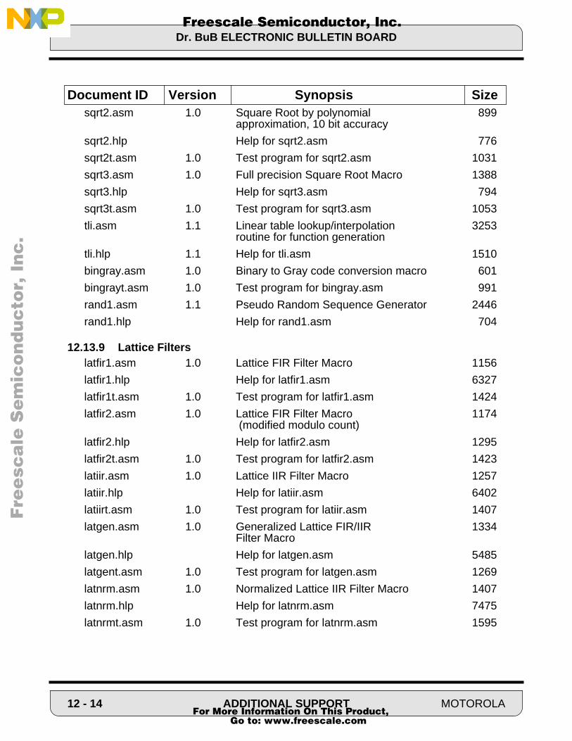
Dr. BuB ELECTRONIC BULLETIN BOARD
Fre
esc
ale
Se
mic
on
du
cto
r, I
Freescale Semiconductor, Inc.n
c..
.
sqrt2.asm 1.0 Square Root by polynomial 899approximation, 10 bit accuracy
sqrt2.hlp Help for sqrt2.asm 776
sqrt2t.asm 1.0 Test program for sqrt2.asm 1031
sqrt3.asm 1.0 Full precision Square Root Macro 1388
sqrt3.hlp Help for sqrt3.asm 794
sqrt3t.asm 1.0 Test program for sqrt3.asm 1053
tli.asm 1.1 Linear table lookup/interpolation 3253routine for function generation
tli.hlp 1.1 Help for tli.asm 1510
bingray.asm 1.0 Binary to Gray code conversion macro 601
bingrayt.asm 1.0 Test program for bingray.asm 991
rand1.asm 1.1 Pseudo Random Sequence Generator 2446
rand1.hlp Help for rand1.asm 704
12.13.9 Lattice Filterslatfir1.asm 1.0 Lattice FIR Filter Macro 1156
latfir1.hlp Help for latfir1.asm 6327
latfir1t.asm 1.0 Test program for latfir1.asm 1424
latfir2.asm 1.0 Lattice FIR Filter Macro 1174 (modified modulo count)
latfir2.hlp Help for latfir2.asm 1295
latfir2t.asm 1.0 Test program for latfir2.asm 1423
latiir.asm 1.0 Lattice IIR Filter Macro 1257
latiir.hlp Help for latiir.asm 6402
latiirt.asm 1.0 Test program for latiir.asm 1407
latgen.asm 1.0 Generalized Lattice FIR/IIR 1334Filter Macro
latgen.hlp Help for latgen.asm 5485
latgent.asm 1.0 Test program for latgen.asm 1269
latnrm.asm 1.0 Normalized Lattice IIR Filter Macro 1407
latnrm.hlp Help for latnrm.asm 7475
latnrmt.asm 1.0 Test program for latnrm.asm 1595
Document ID Version Synopsis Size
12 - 14 ADDITIONAL SUPPORT MOTOROLA For More Information On This Product,
Go to: www.freescale.com

Dr. BuB ELECTRONIC BULLETIN BOARD
Fre
esc
ale
Se
mic
on
du
cto
r, I
Freescale Semiconductor, Inc.n
c..
.
12.13.10 Matrix Operationsmatmul1.asm 1.0 [1x3][3x3]=[1x3] Matrix Multiplication 1817
matmul1.hlp Help for matmul1.asm 527
matmul2.asm 1.0 General Matrix Multiplication, C=AB 2650
matmul2.hlp Help for matmul2.asm 780
matmul3.asm 1.0 General Matrix Multiply-Accumulate, 2815C=AB+Q
matmul3.hlp 1.0 Help for matmul3.asm 865
12.13.11 Reed-Solomon Encoderreadme.rs 1.0 Instructions for Reed-Solomon coding 5200
rscd.asm 1.0 Reed-Solomon coder for DSP56000 simulator 5822
newc.c 1.0 Reed-Solomon coder coded in C 4075
table1.asm 1.0 Include file for R-S coder 7971
table2.asm 1.0 Include file for R-S coder 4011
12.13.12 Sorting Routinessort1.asm 1.0 Array Sort by Straight Selection 1312
sort1.hlp Help for sort1.asm 1908
sort1t.asm 1.0 Test program for sort1.asm 689
sort2.asm 1.1 Array Sort by Heapsort Method 2183
sort2.hlp Help for sort2.asm 2004
sort2t.asm 1.0 Test program for sort2.asm 700
12.13.13 Speechlgsol1.asm 2.0 Leroux-Gueguen solution for PARCOR 4861
(LPC) coefficients
lgsol1.hlp Help for lgsol1.asm 3971
durbin1.asm 1.2 Durbin Solution for PARCOR 6360(LPC) coefficients
durbin1.hlp Help for durbin1.asm 3616
adpcm.asm 1.0 32 kbits/s CCITT ADPCM Speech Coder 120512
adpcm.hlp 1.0 Help file for adpcm.asm 14817
adpcmns.asm 1.0 Nonstandard ADPCM source code 54733
adpcmns.hlp 1.0 Help file for adpcmns.asm 9952
Document ID Version Synopsis Size
MOTOROLA ADDITIONAL SUPPORT 12 - 15 For More Information On This Product,
Go to: www.freescale.com
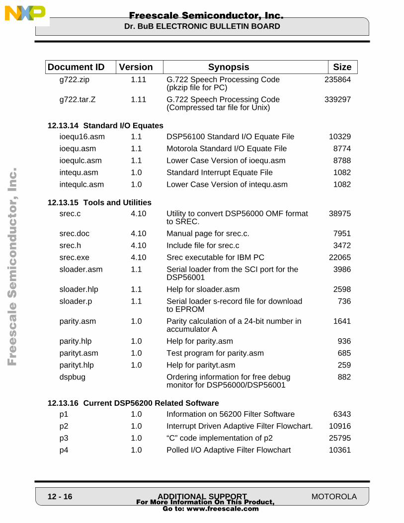
Dr. BuB ELECTRONIC BULLETIN BOARD
Fre
esc
ale
Se
mic
on
du
cto
r, I
Freescale Semiconductor, Inc.n
c..
.
g722.zip 1.11 G.722 Speech Processing Code 235864(pkzip file for PC)
g722.tar.Z 1.11 G.722 Speech Processing Code 339297(Compressed tar file for Unix)
12.13.14 Standard I/O Equatesioequ16.asm 1.1 DSP56100 Standard I/O Equate File 10329
ioequ.asm 1.1 Motorola Standard I/O Equate File 8774
ioequlc.asm 1.1 Lower Case Version of ioequ.asm 8788
intequ.asm 1.0 Standard Interrupt Equate File 1082
intequlc.asm 1.0 Lower Case Version of intequ.asm 1082
12.13.15 Tools and Utilitiessrec.c 4.10 Utility to convert DSP56000 OMF format 38975
to SREC.
srec.doc 4.10 Manual page for srec.c. 7951
srec.h 4.10 Include file for srec.c 3472
srec.exe 4.10 Srec executable for IBM PC 22065
sloader.asm 1.1 Serial loader from the SCI port for the 3986DSP56001
sloader.hlp 1.1 Help for sloader.asm 2598
sloader.p 1.1 Serial loader s-record file for download 736to EPROM
parity.asm 1.0 Parity calculation of a 24-bit number in 1641accumulator A
parity.hlp 1.0 Help for parity.asm 936
parityt.asm 1.0 Test program for parity.asm 685
parityt.hlp 1.0 Help for parityt.asm 259
dspbug Ordering information for free debug 882monitor for DSP56000/DSP56001
12.13.16 Current DSP56200 Related Softwarep1 1.0 Information on 56200 Filter Software 6343
p2 1.0 Interrupt Driven Adaptive Filter Flowchart. 10916
p3 1.0 “C” code implementation of p2 25795
p4 1.0 Polled I/O Adaptive Filter Flowchart 10361
Document ID Version Synopsis Size
12 - 16 ADDITIONAL SUPPORT MOTOROLA For More Information On This Product,
Go to: www.freescale.com

REFERENCE BOOKS AND MANUALS
Fre
esc
ale
Se
mic
on
du
cto
r, I
Freescale Semiconductor, Inc.n
c..
.
p5 1.0 “C” code implementation of p4 24806
p6 1.1 Interrupt Driven Dual FIR Filter Flowchart. 9535
p7 1.0 “C” code implementation of p6 28489
p8 1.0 Polled I/O Dual FIR Filter Flowchart 9656
p9 1.0 “C” code implementation of p8 28525
12.14 REFERENCE BOOKS AND MANUALSA list of DSP-related books is included here as an aid for the engineer who is new to thefield of DSP. This is a partial list of DSP references intended to help the new user finduseful information in some of the many areas of DSP applications. Many books could beincluded in several categories but are not repeated.
12.14.1 General DSPADVANCED TOPICS IN SIGNAL PROCESSING
Jae S. Lim and Alan V. Oppenheim Englewood Cliffs, NJ: Prentice-Hall, Inc., 1988
APPLICATIONS OF DIGITAL SIGNAL PROCESSING A. V. Oppenheim Englewood Cliffs, NJ: Prentice-Hall, Inc., 1978
DISCRETE-TIME SIGNAL PROCESSING A. V. Oppenheim and R. W. Schafer Englewood Cliffs, NJ: Prentice-Hall, Inc., 1989
DIGITAL PROCESSING OF SIGNALS THEORY AND PRACTICE Maurice Bellanger New York, NY: John Wiley and Sons, 1984
DIGITAL SIGNAL PROCESSING Alan V. Oppenheim and Ronald W. Schafer Englewood Cliffs, NJ: Prentice-Hall, Inc., 1975
DIGITAL SIGNAL PROCESSING: A SYSTEM DESIGN APPROACH David J. DeFatta, Joseph G. Lucas, and William S. Hodgkiss New York, NY: John Wiley and Sons, 1988
FOUNDATIONS OF DIGITAL SIGNAL PROCESSING AND DATA ANALYSIS J. A. Cadzow New York, NY: MacMillan Publishing Company, 1987
Document ID Version Synopsis Size
MOTOROLA ADDITIONAL SUPPORT 12 - 17 For More Information On This Product,
Go to: www.freescale.com

REFERENCE BOOKS AND MANUALS
Fre
esc
ale
Se
mic
on
du
cto
r, I
Freescale Semiconductor, Inc.n
c..
.
HANDBOOK OF DIGITAL SIGNAL PROCESSING D. F. Elliott San Diego, CA: Academic Press, Inc., 1987
INTRODUCTION TO DIGITAL SIGNAL PROCESSING John G. Proakis and Dimitris G. Manolakis New York, NY: Macmillan Publishing Company, 1988
MULTIRATE DIGITAL SIGNAL PROCESSING R. E. Crochiere and L. R. Rabiner Englewood Cliffs, NJ: Prentice-Hall, Inc., 1983
SIGNAL PROCESSING ALGORITHMS S. Stearns and R. Davis Englewood Cliffs, NJ: Prentice-Hall, Inc., 1988
SIGNAL PROCESSING HANDBOOK C.H. Chen New York, NY: Marcel Dekker, Inc., 1988
SIGNAL PROCESSING – THE MODERN APPROACH James V. Candy New York, NY: McGraw-Hill Company, Inc., 1988
THEORY AND APPLICATION OF DIGITAL SIGNAL PROCESSING Rabiner, Lawrence R., Gold and Bernard Englewood Cliffs, NJ: Prentice-Hall, Inc., 1975
12.14.2 Digital Audio and FiltersADAPTIVE FILTER AND EQUALIZERS
B. Mulgrew and C. Cowan Higham, MA: Kluwer Academic Publishers, 1988
ADAPTIVE SIGNAL PROCESSING B. Widrow and S. D. Stearns Englewood Cliffs, NJ: Prentice-Hall, Inc., 1985
ART OF DIGITAL AUDIO, THE John Watkinson Stoneham. MA: Focal Press, 1988
DESIGNING DIGITAL FILTERS Charles S. Williams Englewood Cliffs, NJ: Prentice-Hall, Inc., 1986
DIGITAL AUDIO SIGNAL PROCESSING AN ANTHOLOGY John Strawn William Kaufmann, Inc., 1985
12 - 18 ADDITIONAL SUPPORT MOTOROLA For More Information On This Product,
Go to: www.freescale.com

REFERENCE BOOKS AND MANUALS
Fre
esc
ale
Se
mic
on
du
cto
r, I
Freescale Semiconductor, Inc.n
c..
.
DIGITAL CODING OF WAVEFORMS N. S. Jayant and Peter Noll Englewood Cliffs, NJ: Prentice-Hall, Inc., 1984
DIGITAL FILTERS: ANALYSIS AND DESIGN Andreas Antoniou New York, NY: McGraw-Hill Company, Inc., 1979
DIGITAL FILTERS AND SIGNAL PROCESSING Leland B. Jackson Higham, MA: Kluwer Academic Publishers, 1986
DIGITAL SIGNAL PROCESSING Richard A. Roberts and Clifford T. Mullis New York, NY: Addison-Welsey Publishing Company, Inc., 1987
INTRODUCTION TO DIGITAL SIGNAL PROCESSING Roman Kuc New York, NY: McGraw-Hill Company, Inc., 1988
INTRODUCTION TO ADAPTIVE FILTERS Simon Haykin New York, NY: MacMillan Publishing Company, 1984
MUSICAL APPLICATIONS OF MICROPROCESSORS (Second Edition) H. Chamberlin Hasbrouck Heights, NJ: Hayden Book Co., 1985
12.14.3 C Programming LanguageC: A REFERENCE MANUAL
Samuel P. Harbison and Guy L. SteelePrentice-Hall Software Series, 1987.
PROGRAMMING LANGUAGE - CAmerican National Standards Institute, ANSI Document X3.159-1989American National Standards Institute, inc., 1990
THE C PROGRAMMING LANGUAGEBrian W. Kernighan, and Dennis M. RitchiePrentice-Hall, Inc., 1978.
12.14.4 ControlsADAPTIVE CONTROL
K. Astrom and B. Wittenmark New York, NY: Addison-Welsey Publishing Company, Inc., 1989
MOTOROLA ADDITIONAL SUPPORT 12 - 19 For More Information On This Product,
Go to: www.freescale.com

REFERENCE BOOKS AND MANUALS
Fre
esc
ale
Se
mic
on
du
cto
r, I
Freescale Semiconductor, Inc.n
c..
.
ADAPTIVE FILTERING PREDICTION & CONTROL G. Goodwin and K. Sin Englewood Cliffs, NJ: Prentice-Hall, Inc., 1984
AUTOMATIC CONTROL SYSTEMS B. C. Kuo Englewood Cliffs, NJ: Prentice-Hall, Inc., 1987
COMPUTER CONTROLLED SYSTEMS: THEORY & DESIGN K. Astrom and B. Wittenmark Englewood Cliffs, NJ: Prentice-Hall, Inc., 1984
DIGITAL CONTROL SYSTEMS B. C. Kuo New York, NY: Holt, Reinholt, and Winston, Inc., 1980
DIGITAL CONTROL SYSTEM ANALYSIS & DESIGN C. Phillips and H. Nagle Englewood Cliffs, NJ: Prentice-Hall, Inc., 1984
ISSUES IN THE IMPLEMENTATION OF DIGITAL FEEDBACK COMPENSATORS P. Moroney Cambridge, MA: The MIT Press, 1983
12.14.5 GraphicsCGM AND CGI
D. B. Arnold and P. R. Bono New York, NY: Springer-Verlag, 1988
COMPUTER GRAPHICS (Second Edition) D. Hearn and M. Pauline Baker Englewood Cliffs, NJ: Prentice-Hall, Inc., 1986
FUNDAMENTALS OF INTERACTIVE COMPUTER GRAPHICS J. D. Foley and A. Van Dam Reading MA: Addison-Wesley Publishing Company Inc., 1984
GEOMETRIC MODELING Michael E. Morteson New York, NY: John Wiley and Sons, Inc.
GKS THEORY AND PRACTICE P. R. Bono and I. Herman (Eds.) New York, NY: Springer-Verlag, 1987
ILLUMINATION AND COLOR IN COMPUTER GENERATED IMAGERY Roy Hall New York, NY: Springer-Verlag
12 - 20 ADDITIONAL SUPPORT MOTOROLA For More Information On This Product,
Go to: www.freescale.com
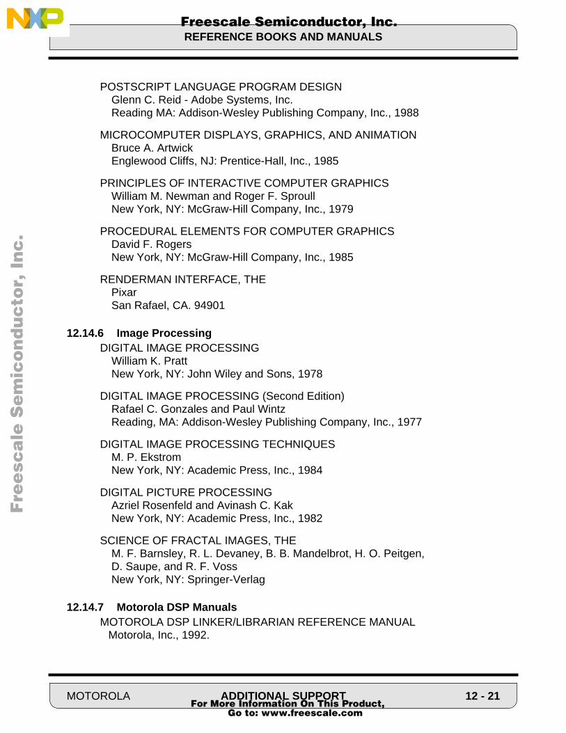
REFERENCE BOOKS AND MANUALS
F
ree
sca
le S
em
ico
nd
uc
tor,
I
Freescale Semiconductor, Inc.n
c..
.
POSTSCRIPT LANGUAGE PROGRAM DESIGN Glenn C. Reid - Adobe Systems, Inc. Reading MA: Addison-Wesley Publishing Company, Inc., 1988
MICROCOMPUTER DISPLAYS, GRAPHICS, AND ANIMATION Bruce A. Artwick Englewood Cliffs, NJ: Prentice-Hall, Inc., 1985
PRINCIPLES OF INTERACTIVE COMPUTER GRAPHICS William M. Newman and Roger F. Sproull New York, NY: McGraw-Hill Company, Inc., 1979
PROCEDURAL ELEMENTS FOR COMPUTER GRAPHICS David F. Rogers New York, NY: McGraw-Hill Company, Inc., 1985
RENDERMAN INTERFACE, THE Pixar San Rafael, CA. 94901
12.14.6 Image ProcessingDIGITAL IMAGE PROCESSING
William K. Pratt New York, NY: John Wiley and Sons, 1978
DIGITAL IMAGE PROCESSING (Second Edition) Rafael C. Gonzales and Paul Wintz Reading, MA: Addison-Wesley Publishing Company, Inc., 1977
DIGITAL IMAGE PROCESSING TECHNIQUES M. P. Ekstrom New York, NY: Academic Press, Inc., 1984
DIGITAL PICTURE PROCESSING Azriel Rosenfeld and Avinash C. Kak New York, NY: Academic Press, Inc., 1982
SCIENCE OF FRACTAL IMAGES, THE M. F. Barnsley, R. L. Devaney, B. B. Mandelbrot, H. O. Peitgen, D. Saupe, and R. F. Voss New York, NY: Springer-Verlag
12.14.7 Motorola DSP ManualsMOTOROLA DSP LINKER/LIBRARIAN REFERENCE MANUAL
Motorola, Inc., 1992.
MOTOROLA ADDITIONAL SUPPORT 12 - 21 For More Information On This Product,
Go to: www.freescale.com

REFERENCE BOOKS AND MANUALS
F
ree
sca
le S
em
ico
nd
uc
tor,
I
Freescale Semiconductor, Inc.n
c..
.
MOTOROLA DSP ASSEMBLER REFERENCE MANUALMotorola, Inc., 1992.
MOTOROLA DSP SIMULATOR REFERENCE MANUALMotorola, Inc., 1992.
MOTOROLA DSP56000/DSP56001 USER’S MANUALMotorola, Inc.,1990.
MOTOROLA DSP56100 FAMILY MANUALMotorola, Inc.,1992.
MOTOROLA DSP56156 USER’S MANUALMotorola, Inc.,1992.
MOTOROLA DSP56166 USER’S MANUALMotorola, Inc.,1992.
MOTOROLA DSP96002 USER’S MANUALMotorola, Inc.,1989.
12.14.8 Numerical MethodsALGORITHMS (THE CONSTRUCTION, PROOF, AND ANALYSIS OF
PROGRAMS) P. Berliout and P. Bizard New York, NY: John Wiley and Sons, 1986
MATRIX COMPUTATIONS G. H. Golub and C. F. Van Loan John Hopkins Press, 1983
NUMERICAL RECIPES IN C - THE ART OF SCIENTIFIC PROGRAMMING William H. Press, Brian P. Flannery, Saul A. Teukolsky, and William T. Vetterling Cambridge University Press, 1988
NUMBER THEORY IN SCIENCE AND COMMUNICATION Manfred R. Schroeder New York, NY: Springer-Verlag, 1986
12.14.9 Pattern RecognitionPATTERN CLASSIFICATION AND SCENE ANALYSIS
R. O. Duda and P. E. Hart New York, NY: John Wiley and Sons, 1973
12 - 22 ADDITIONAL SUPPORT MOTOROLA For More Information On This Product,
Go to: www.freescale.com

REFERENCE BOOKS AND MANUALS
F
ree
sca
le S
em
ico
nd
uc
tor,
I
Freescale Semiconductor, Inc.n
c..
.
CLASSIFICATION ALGORITHMS Mike James New York, NY: Wiley-Interscience, 1985Spectral Analysis:
STATISTICAL SPECTRAL ANALYSIS, A NONPROBABILISTIC THEORY William A. Gardner Englewood Cliffs, NJ: Prentice-Hall, Inc., 1988
THE FAST FOURIER TRANSFORM AND ITS APPLICATIONS E. Oran Brigham Englewood Cliffs, NJ: Prentice-Hall, Inc., 1988
THE FAST FOURIER TRANSFORM AND ITS APPLICATIONS R. N. Bracewell New York, NY: McGraw-Hill Company, Inc., 1986
12.14.10 SpeechADAPTIVE FILTERS – STRUCTURES, ALGORITHMS, AND APPLICATIONS
Michael L. Honig and David G. Messerschmitt Higham, MA: Kluwer Academic Publishers, 1984
DIGITAL CODING OF WAVEFORMS N. S. Jayant and P. Noll Englewood Cliffs, NJ: Prentice-Hall, Inc., 1984
DIGITAL PROCESSING OF SPEECH SIGNALS Lawrence R. Rabiner and R. W. Schafer Englwood Cliffs, NJ: Prentice-Hall, Inc., 1978
LINEAR PREDICTION OF SPEECH J. D. Markel and A. H. Gray, Jr. New York, NY: Springer-Verlag, 1976
SPEECH ANALYSIS, SYNTHESIS, AND PERCEPTION J. L. Flanagan New York, NY: Springer-Verlag, 1972
SPEECH COMMUNICATION – HUMAN AND MACHINE D. O’Shaughnessy Reading, MA: Addison-Wesley Publishing Company, Inc., 1987
12.14.11 TelecommunicationsDIGITAL COMMUNICATION
Edward A. Lee and David G. Messerschmitt Higham, MA: Kluwer Academic Publishers, 1988
MOTOROLA ADDITIONAL SUPPORT 12 - 23 For More Information On This Product,
Go to: www.freescale.com

REFERENCE BOOKS AND MANUALS
F
ree
sca
le S
em
ico
nd
uc
tor,
I
Freescale Semiconductor, Inc.n
c..
.
DIGITAL COMMUNICATIONS John G. Proakis New York, NY: McGraw-Hill Publishing Co., 1983
12 - 24 ADDITIONAL SUPPORT MOTOROLA For More Information On This Product,
Go to: www.freescale.com
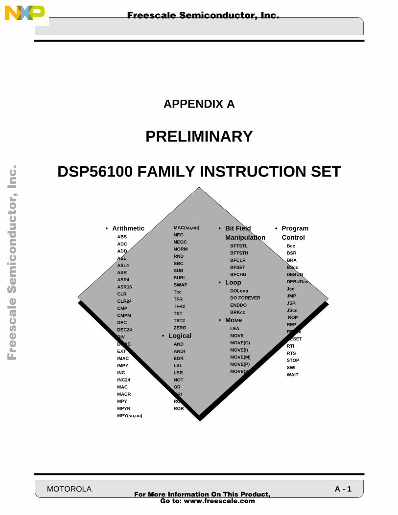
Fre
esc
ale
Se
mic
on
du
cto
r, I
Freescale Semiconductor, Inc.n
c..
.
APPENDIX A
PRELIMINARY
DSP56100 FAMILY INSTRUCTION SET
• Bit Field Manipulation
BFTSTL
BFTSTH
BFCLR
BFSET
BFCHG
• LoopDOLoop
DO FOREVER
ENDDO
BRKcc
• MoveLEA
MOVE
MOVE(C)
MOVE(I)
MOVE(M)
MOVE(P)
MOVE(S)
• ArithmeticABS
ADC
ADD
ASL
ASL4
ASR
ASR4
ASR16
CLR
CLR24
CMP
CMPM
DEC
DEC24
DIV
DMAC
EXT
IMAC
IMPY
INC
INC24
MAC
MACR
MPY
MPYR
MPY(su,uu)
MAC(su,uu)
NEG
NEGC
NORM
RND
SBC
SUB
SUBL
SWAP
Tcc
TFR
TFR2
TST
TST2
ZERO
• LogicalAND
ANDI
EOR
LSL
LSR
NOT
OR
ORI
ROL
ROR
• Program Control
Bcc
BSR
BRA
BScc
DEBUG
DEBUGcc
Jcc
JMP
JSR
JScc
NOP
REP
REPcc
RESET
RTI
RTS
STOP
SWI
WAIT
MOTOROLA
For More Information OGo to: www.fre
n This Product,escale.com
A - 1

SECTION CONTENTS
Fre
esc
ale
Se
mic
on
du
cto
r, I
Freescale Semiconductor, Inc.n
c..
.
A.1 INTRODUCTION . . . . . . . . . . . . . . . . . . . . . . . . . . . . . . . . . . . . . . . . A-3A.1.1 Instruction Guide . . . . . . . . . . . . . . . . . . . . . . . . . . . . . . . . . . . . . . . . . A-3A.2 NOTATION . . . . . . . . . . . . . . . . . . . . . . . . . . . . . . . . . . . . . . . . . . . . . A-4A.3 ADDRESSING MODES . . . . . . . . . . . . . . . . . . . . . . . . . . . . . . . . . . . A-8A.3.1 Addressing Mode Modifiers . . . . . . . . . . . . . . . . . . . . . . . . . . . . . . . . A-11A.4 CONDITION CODE COMPUTATION . . . . . . . . . . . . . . . . . . . . . . . . . A-12A.5 DESCRIPTIONS . . . . . . . . . . . . . . . . . . . . . . . . . . . . . . . . . . . . . . . . . A-17A.6 INSTRUCTION TIMING . . . . . . . . . . . . . . . . . . . . . . . . . . . . . . . . . . . A-226A.7 FUNCTIONAL SUMMARY . . . . . . . . . . . . . . . . . . . . . . . . . . . . . . . . . A-236
A - 2 MOTOROLA For More Information On This Product,
Go to: www.freescale.com
INTRODUCTION
Fre
esc
ale
Se
mic
on
du
cto
r, I
Freescale Semiconductor, Inc.n
c..
.
A.1 INTRODUCTION
This appendix contains detailed information about each instruction in the DSP56100 family instruction set.An instruction guide is presented first to help in understanding the individual instruction descriptions. Thisis followed by sections on notation and addressing modes. Since the move instruction is a parallel movewith an ALU NOP, the parallel moves are grouped with the MOVE instruction. The instructions are then de-scribed in alphabetical order.
A.1.1 Instruction Guide
The following information is included in each instruction description with the goal of making each descriptionself-contained:
Name and Mnemonic: The mnemonic is highlighted in bold type for easy reference.
Assembler Syntax and Operation: For each instruction syntax the corresponding operation is symbolicallydescribed. If there are several operations indicated on a single line in the operation field, those operationsdo not necessarily occur in the order shown but are generally assumed to occur in parallel. If a parallel datamove is allowed it will be indicated in parenthesis in both the assembler syntax and operation fields. If aletter in the mnemonic is optional it will be shown in parenthesis in the assembler syntax field.
Description: A complete text description of the instruction is given together with any special cases and/orcondition code anomalies which the user should be aware of when using that instruction.
Example: An example of the use of the instruction is given. The example is shown in the DSP56100 assem-bler source code format. Most arithmetic and logical instruction examples include one or two parallel datamoves to illustrate the many types of parallel moves that are possible. The example includes a completeexplanation which discusses the contents of the registers referenced by the instruction (but not those refer-enced by the parallel moves) both before and after the execution of the instruction. Most examples are de-signed to be easily understood without the use of a calculator. The contents shown in registers are in hexa-decimal format.
Condition Codes: The status register is depicted with the condition code bits which can be affected by theinstruction highlighted in bold type. Not all bits in the status register are used. Those which are reserved areindicated with a double asterisk and are read as zeros.
Instruction Format: The instruction fields, the instruction opcode and the instruction extension word arespecified for each instruction syntax. When the extension word is optional it is so indicated. The valueswhich can be assumed by each of the variables in the various instruction fields are shown under the instruc-tion fields heading. Note that the symbols used in decoding the various opcode fields of an instruction arecompletely arbitrary. Furthermore, the opcode symbols used in one instruction are completely independentof the opcode symbols used in a different instruction.
Timing: The number of oscillator clock cycles required for each instruction syntax is given. This informationprovides the user a basis for comparison of the execution times of the various instructions in oscillator clock
MOTOROLA A - 3 For More Information On This Product,
Go to: www.freescale.com

NOTATION
Fre
esc
ale
Se
mic
on
du
cto
r, I
Freescale Semiconductor, Inc.n
c..
.
cycles. Please refer to Table A-1 and the section entitled “Instruction Timing” for a complete explanationof instruction timing including the meaning of the symbols “aio”, “ap”, “ax”, “ax2”, “ea”, “jx”, “mv”, “mvb”,“mvc”, “mvm”, “mvp”, “rx”, “wio”, “wp”, and “wx”.
Memory: The number of program memory words required for each instruction syntax is given. This informa-tion provides the user a basis for comparison of the number of program memory locations required for eachof the various instructions in 16-bit program memory words. Please refer to Table A-1 and the section enti-tled “Instruction Timing” for a complete explanation of instruction memory requirements including themeaning of the symbols “ea” and “mv”.
A.2 NOTATION
Each instruction description contains symbols used to abbreviate certain operands and operations. TableA-1 lists the symbols used and their respective meanings.
Table A-1 Instruction Description Notation
Data ALU Registers Operands
Xn Input register X1 or X0 (16 bits)Yn Input register Y1 or Y0 (16 bits)An Accumulator registers A2, A1, A0 (A2 - 8 bits, A1 and A0 - 16 bits)Bn Accumulator registers B2, B1, B0 (B2 - 8 bits, B1 and B0 - 16 bits)X Input register X = X1:X0 (32 bits)Y Input register Y = Y1:Y0 (32 bits)A Accumulator A = A2:A1:A0 (40 bits) *B Accumulator B = B2:B1:B0 (40 bits) *
* Note: In data move operations, shifting and limiting is performed when this register is specified as asource operand. When specified as a destination operand, sign extension and possibly zero-ing are performed.
A - 4 MOTOROLA For More Information On This Product,
Go to: www.freescale.com
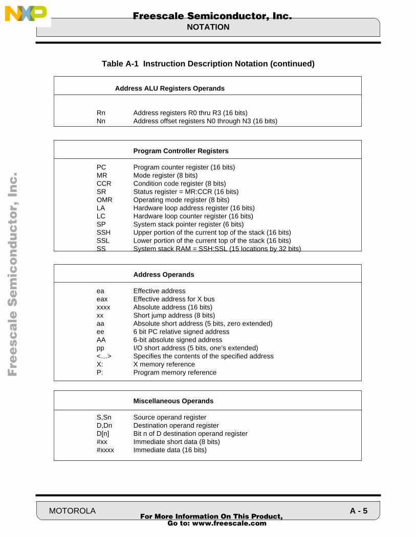
NOTATION
Fre
esc
ale
Se
mic
on
du
cto
r, I
Freescale Semiconductor, Inc.n
c..
.
Table A-1 Instruction Description Notation (continued)
Address ALU Registers Operands
Rn Address registers R0 thru R3 (16 bits)Nn Address offset registers N0 through N3 (16 bits)
Program Controller Registers
PC Program counter register (16 bits)MR Mode register (8 bits)CCR Condition code register (8 bits)SR Status register = MR:CCR (16 bits)OMR Operating mode register (8 bits)LA Hardware loop address register (16 bits)LC Hardware loop counter register (16 bits)SP System stack pointer register (6 bits)SSH Upper portion of the current top of the stack (16 bits)SSL Lower portion of the current top of the stack (16 bits)SS System stack RAM = SSH:SSL (15 locations by 32 bits)
Address Operands
ea Effective addresseax Effective address for X busxxxx Absolute address (16 bits)xx Short jump address (8 bits)aa Absolute short address (5 bits, zero extended) ee 6 bit PC relative signed addressAA 6-bit absolute signed addresspp I/O short address (5 bits, one’s extended)<…> Specifies the contents of the specified addressX: X memory referenceP: Program memory reference
Miscellaneous Operands
S,Sn Source operand registerD,Dn Destination operand registerD[n] Bit n of D destination operand register#xx Immediate short data (8 bits)#xxxx Immediate data (16 bits)
MOTOROLA A - 5 For More Information On This Product,
Go to: www.freescale.com

NOTATION
Fre
esc
ale
Se
mic
on
du
cto
r, I
Freescale Semiconductor, Inc.n
c..
.
Table A-1 Instruction Description Notation (continued)
Unary Operators
x The over bar is the negation operatorPUSH Push specified value onto the system stack (SS) operatorPULL Pull specified value from the system stack (SS) operatorREAD Read the top of the system stack (SS) operatorPURGE Delete the top value on the system stack (SS) operator| | Absolute value operator
Binary Operators
+ Addition operator- Subtraction operator* Multiplication operator÷,/ Division operator+ Logical inclusive OR operator|,• Logical AND operator⊕ Logical exclusive OR operator→ “Is transferred to” operator: Concatenation operatorSS System stack RAM = SSH:SSL (15 locations by 32 bits)
Addressing Mode Operators
<< I/O short addressing mode force operator< Short addressing mode force operator> Long addressing mode force operator# Immediate addressing mode operator#> Immediate long addressing mode force operator#< Immediate short addressing mode force operator
Mode Register (MR) Symbols
LF Loop Flag bit indicating when a DO loop is in progressFV ForeVer flag bit indicating when a DOFOREVER loop is in progress
S1,S0 Scaling Mode bits indicating the current scaling modeI1,I0 Interrupt Mask bits indicating the current interrupt priority level
A - 6 MOTOROLA For More Information On This Product,
Go to: www.freescale.com
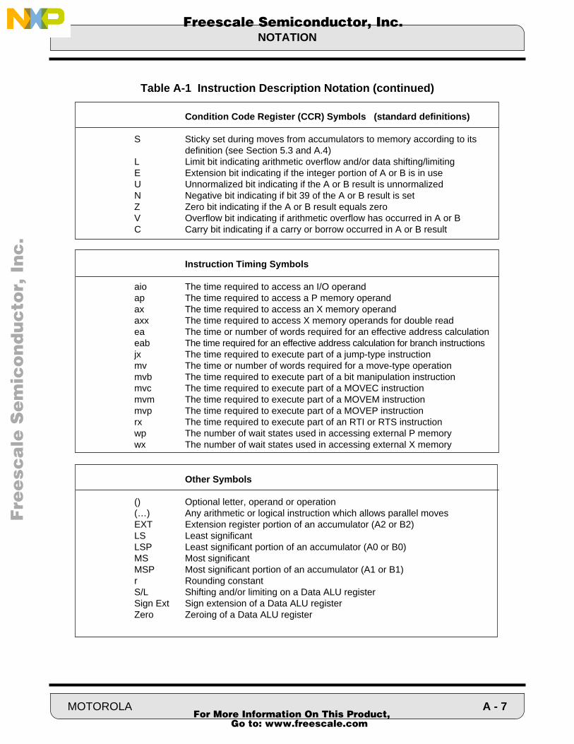
NOTATION
Fre
esc
ale
Se
mic
on
du
cto
r, I
Freescale Semiconductor, Inc.n
c..
.
Table A-1 Instruction Description Notation (continued)
Condition Code Register (CCR) Symbols (standard definitions)
S Sticky set during moves from accumulators to memory according to its definition (see Section 5.3 and A.4)
L Limit bit indicating arithmetic overflow and/or data shifting/limitingE Extension bit indicating if the integer portion of A or B is in useU Unnormalized bit indicating if the A or B result is unnormalizedN Negative bit indicating if bit 39 of the A or B result is setZ Zero bit indicating if the A or B result equals zeroV Overflow bit indicating if arithmetic overflow has occurred in A or BC Carry bit indicating if a carry or borrow occurred in A or B result
Instruction Timing Symbols
aio The time required to access an I/O operandap The time required to access a P memory operandax The time required to access an X memory operandaxx The time required to access X memory operands for double readea The time or number of words required for an effective address calculation eab The time required for an effective address calculation for branch instructionsjx The time required to execute part of a jump-type instructionmv The time or number of words required for a move-type operationmvb The time required to execute part of a bit manipulation instructionmvc The time required to execute part of a MOVEC instructionmvm The time required to execute part of a MOVEM instructionmvp The time required to execute part of a MOVEP instructionrx The time required to execute part of an RTI or RTS instructionwp The number of wait states used in accessing external P memorywx The number of wait states used in accessing external X memory
Other Symbols
() Optional letter, operand or operation (…) Any arithmetic or logical instruction which allows parallel movesEXT Extension register portion of an accumulator (A2 or B2)LS Least significantLSP Least significant portion of an accumulator (A0 or B0)MS Most significantMSP Most significant portion of an accumulator (A1 or B1)r Rounding constant S/L Shifting and/or limiting on a Data ALU registerSign Ext Sign extension of a Data ALU registerZero Zeroing of a Data ALU register
MOTOROLA A - 7 For More Information On This Product,
Go to: www.freescale.com

ADDRESSING MODES
Fre
esc
ale
Se
mic
on
du
cto
r, I
Freescale Semiconductor, Inc.n
c..
.
A.3 ADDRESSING MODES
The addressing modes are grouped into three categories — register direct, address register indirect andspecial. These addressing modes are summarized in Table A-2. All address calculations are performed inthe Address ALU to minimize execution time and loop overhead. Addressing modes specify whether theoperands are in registers, in memory or in the instruction itself (such as immediate data) and provide thespecific address of the operands.
The register direct addressing mode can be subclassified according to the specific register addressed. Thedata registers include X1, X0, Y1, Y0, X, Y, A2, A1, A0, B2, B1, B0, A, and B. The control registers includeSR, OMR, SP, SSH, SSL, LA, LC, CCR, and MR.
Address register indirect modes use an address register Rn (R0-R3) to point to locations in X and P mem-ory. The contents of the Rn address register is the effective address of the specified operand, except in the“indexed by offset” mode where the effective address is (Rn+Nn). Address register indirect modes use anaddress modifier register Mn to specify the type of arithmetic to be used to generate the ea. If an addressingmode specifies an address offset register, the given address offset register is used to update the corre-sponding address register. The Rn address register may only use the corresponding address offset registerNn and the corresponding address modifier register Mn. For example, the address register R0 may only usethe N0 address offset register and the M0 address modifier register during actual address computation andaddress register update operations. This unique implementation is extremely powerful and allows the userto easily address a wide variety of DSP oriented data structures. All address register indirect modes use atleast one set of address registers (Rn, Nn, and Mn), and the double X memory read uses two sets of ad-dress registers, one for the first X memory read and one for the second X memory read. Only R3:N3 canbe used for this second X memory read and R3 is updated only using the linear arithmetic.
The special addressing modes include immediate and absolute addressing modes as well as implied refer-ences to the program counter (PC), the system stack (SSH or SSL), and program (P) memory.
Addressing modes may also be categorized by the ways in which they may be used. Table A-3 shows thevarious categories to which each addressing mode belongs. The following classifications will be used in theinstruction descriptions.
A - 8 MOTOROLA For More Information On This Product,
Go to: www.freescale.com

ADDRESSING MODES
Fre
esc
ale
Se
mic
on
du
cto
r, I
Freescale Semiconductor, Inc.n
c..
.
Table A-2 DSP56100 Family Addressing Modes
Operand ReferenceUses Mn
Addressing Mode Modifier S C D A P X XX
Register Direct
Data or Control Register No X X XAddress Register Rn No XAddress Modifier Register Mn No XAddress Offset Register Nn No X
Address Register Indirect
No Update No X XPostincrement by 1 Yes* X X XPostdecrement by 1 Yes X XPostincrement by Offset Nn Yes* X X XIndexed by Offset Nn Yes XPredecrement by 1 Yes X
PC Relative
Long Displacement No XShort Displacement No X XAddress Register No X X
Special
Upper word of accumulator No XImmediate Data No XImmediate Short Data No XAbsolute Address No X XAbsolute Short Address No X XShort Jump Address No XI/O Short Address No XImplicit No X X XIndexed by short displacement No X
Where:S = System Stack ReferenceP = Program Memory ReferenceC =Program Controller Register ReferenceX = X Memory ReferenceD = Data ALU Register ReferenceXX = Double X Memory ReadA = Address ALU Register Reference
*note: M3 is not used for updating R3 in the second read in the X memory
MOTOROLA A - 9 For More Information On This Product,
Go to: www.freescale.com

ADDRESSING MODES
Fre
esc
ale
Se
mic
on
du
cto
r, I
Freescale Semiconductor, Inc.n
c..
.
Table A-3 DSP56100 Family Addressing Mode Encoding
The address register indirect addressing modes require that the offset register number be the same as theaddress register number. The assembler syntax “Nn” supports this feature. The assembler syntax “N” maybe used instead of “Nn” in the address register indirect memory addressing modes. If “N” is specified, theoffset register number is the same as the address register number.
Addressing Categories
AssemblerAddressing Mode U P M A Syntax
Register Direct
Data or Control Register X (Table A-1)Address Register X RnAddress Offset Register X NnAddress Modifier Register X Mn
Address Register Indirect
No Update X X (Rn)Postincrement by 1 X X X X (Rn)+Postdecrement by 1 X X (Rn)-Postincrement by Offset Nn X X X X (Rn)+NnIndexed by Offset Nn X X (Rn+Nn)Predecrement by 1 X X -(Rn)
Special
Upper word of accumulator X X (A1) or (B1)Immediate Data X #xxxxAbsolute Address X X xxxxImmediate Short Data #xxShort Jump/Branch Address X AA or eeAbsolute Short Address X aaI/O Short Address X ppImplicit XIndexed by short displacement X X R2+xx
Where:Update Mode (U) The Update Addressing mode is used to modify registers without
any associated data moveParallel Mode (P) The Parallel Addressing mode is used in instructions where two
effective addresses are requiredMemory Mode (M) The Memory Addressing mode is used to refer to operands in
memory using an effective addressing fieldAlterable Mode (A) The Alterable Addressing mode is used to refer to alterable or writ-
A - 10 MOTOROLA For More Information On This Product,
Go to: www.freescale.com

ADDRESSING MODES
Fre
esc
ale
Se
mic
on
du
cto
r, I
Freescale Semiconductor, Inc.n
c..
.
A.3.1 Addressing Mode Modifiers
The addressing mode selected in the instruction word is further specified by the contents of the addressmodifier register Mn. The addressing mode update modifiers (M0-M3) are shown in Table A-4. There areno restrictions on the use of modifier types with any address register indirect addressing mode.
Table A-4 Addressing Mode Modifier Summary
16-bit Modifier Reg. (M0-M3)MMMMMMMMMMMMMMMM Address Calculation Arithmetic
0000000000000000 Reverse Carry (Bit Reversed)0000000000000001 Modulo 20000000000000010 Modulo 3
0111111111111110 Modulo 327670111111111111111 Modulo 32768
1000000000000000 Reserved
1111111111111110 Reserved1111111111111111 Linear (Modulo 65536)
where MMMMMMMMMMMMMMMM = 16-bit Modifier Register Contents
MOTOROLA A - 11 For More Information On This Product,
Go to: www.freescale.com

CONDITION CODE COMPUTATION
Fre
esc
ale
Se
mic
on
du
cto
r, I
Freescale Semiconductor, Inc.n
c..
.
A.4 CONDITION CODE COMPUTATION
The condition code portion of the status register consists of 8 defined bits:
C — Carry
V — Overflow
Z — Zero
N — Negative
U — Unnormalized
E — Extension
L — Limit
S — Sticky
The C,V,Z,N,U,E, and S bits are true condition code bits that reflect the condition of the result of a data ALUoperation. These condition code bits are not affected by address ALU calculations or by data transfers (ex-cept for the S and L bits) over the XDB, GDB data buses. The L bit is a latching overflow bit which indicatesthat an overflow has occurred in the Data ALU or that limiting has occurred when reading a Data ALU reg-ister. This limiting occurs as the result of a data bus move operation with limiting accumulator data throughthe data shifter/limiters. The S bit is a latching bit useful in implementing block floating point FFT algorithms.When a move to X memory from an accumulator is made, the S bit is set to indicate that scaling should beimplemented on the next FFT pass.
The standard definition of the condition codes is given below. Exceptions to these are given in Table A-5.
C (Carry) Set if a carry is generated out of the most significant bit of the result for an addition.Also set if borrow is generated in a subtraction. The carry or borrow is generated outof bit 39 of the result. Clear otherwise.
V (Overflow) Set if an arithmetic overflow occurs in the 40 bit result. This indicates that the resultis not representable in the accumulator register and the accumulator register hasoverflowed. Cleared otherwise. In Saturation Mode, an arithmetic overflow occursin the 32 bit result. This indicates that the result is not representable in the accumu-lator register without the extension part. The accumulator register has overflowed.Cleared otherwise.
Z (Zero) Set if the result equals zero. Cleared otherwise.
N (Negative) Set if the most significant bit, bit 39, of the result is set. Cleared otherwise.
U (Unnormalized) Set if the two most significant bits of the MSP portion of the result are the same.Cleared otherwise. The MSP portion is defined by the scaling mode and the U bit iscomputed as follows:
S1 S0 Scaling Mode U bit Computation
0 0 No scaling U = (Bit 31⊕ Bit 30) 0 1 Scale down U = (Bit 32 ⊕ Bit 31) 1 0 Scale up U = (Bit 30 ⊕ Bit 29)
A - 12 MOTOROLA For More Information On This Product,
Go to: www.freescale.com

CONDITION CODE COMPUTATION
Fre
esc
ale
Se
mic
on
du
cto
r, I
Freescale Semiconductor, Inc.n
c..
.
E (Extension) Cleared if all the bits of the integer portion of the result are the same; that is, the bit patterns 00…00 or 11…11. Set otherwise. The integer portion is defined by the scal-ing mode and the E bit is computed as follows:
If E is cleared, then the low-order fractional portion contains all the significant bits and the high order integer portion is sign extended. In this case, the accumulator exten-sion register can be ignored. This flag is meaningless if saturation has occurred (the saturation flag is set, SAT=1).
L (Limit) Set if the overflow bit V is set. Also set if the data shifter/limiters perform a limiting operation. In Saturation Mode, the L limit is set by the saturation of the 32 bit result. Not affected otherwise. The L bit is latched once it is set. The L bit is cleared only by the processor reset or an instruction that explicitly clears it. The L bit is affected by data movement operations which read the accumulator registers.
S (Sticky) Set on moves of accumulators to X memory. This can happen when using a MOVE instruction or in a parallel move. The S bit is computed according to scaling modes as follows:
Note: The S bit is a “sticky” bit in the status register. It is cleared only during reset, ANDI operation, or a move to the status register.
S1 S0 Scaling Mode Integer Portion
0 0 No scaling Bits 39,38,…,32,31 0 1 Scale down Bits 39,38,…,32 1 0 Scale up Bits 39,38,…,32,31,30
S1 S0 Scaling Mode Integer Portion
0 0 No scaling S=Bit 30 ⊕ Bit 29 0 1 Scale down S=Bit 31 ⊕ Bit 30 1 0 Scale up S=Bit 29 ⊕ Bit28
MOTOROLA A - 13 For More Information On This Product,
Go to: www.freescale.com

CONDITION CODE COMPUTATION
Fre
esc
ale
Se
mic
on
du
cto
r, I
Freescale Semiconductor, Inc.n
c..
.
Figure A-1 details how each instruction affects the condition codes. The convention for the notation that isused in the condition code register representation is:
* set according to the standard definition by the result of the operation
— not affected by the operation
0 cleared
1 set
U undefined, meaningless
? set according to the special computation definition by the result of the operation.
Note that the condition code computation shown in Table A-5 may differ from that defined in the opcodedescriptions. This indicates that the standard definition may be used to generate the specific condition coderesult. For example, the Z flag computation for the CLR instruction is shown below as the standard definitionwhile the opcode description indicates that the Z flag is always set. Table A-5 gives the chip implementationviewpoint while the opcode description gives the user viewpoint.
A - 14 MOTOROLA For More Information On This Product,
Go to: www.freescale.com

CONDITION CODE COMPUTATION
Fre
esc
ale
Se
mic
on
du
cto
r, I
Freescale Semiconductor, Inc.n
c..
.
Table A-5 Condition Code Computations
MOTOROLA A - 15 For More Information On This Product,
Go to: www.freescale.com
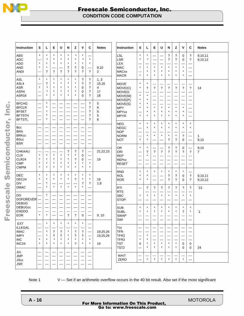
CONDITION CODE COMPUTATION
Instru
ABSADCADDANDANDI
ASLASL4ASRASR4ASR16
BFCHGBFCLRBFSETBFTSTBFTST
BccBRABRKccBSccBSR
CHKACLRCLR24CMPCMPM
DECDEC24DIVDMAC
DODOFODEBUDEBUENDDEOR
EXTILLEGIMACIMPYINCINC24
JccJMPJSccJSR
F
ree
sca
le S
em
ico
nd
uc
tor,
I
Freescale Semiconductor, Inc.n
c..
.
Note 1 V — Set if an arithmetic overflow occurs in the 40 bit result. Also set if the most significant
Instruction S L E U N Z V C Notes
LSL * * — — ? ? 0 ? 9,10,11LSR * * — — ? ? 0 ? 9,10,12LEA — — — — — — — — MAC * * * * * * * —MACxx — * * * * * * —MACR * * * * * * * —
MOVE * * — — — — — —MOVE(C) * ? ? ? ? ? ? ? 14MOVE(I) — — — — — — — —MOVE(M) * * — — — — — —MOVE(P) * * — — — — — —MOVE(S) * * — — — — — —MPY * * * * * * * —MPYxx — * * * * * * —MPYR * * * * * * * —
NEG * * * * * * * *NEGC — * * * * * * * NOP — — — — — — — —NORM — * * * * * ? — 1NOT * * — — ? ? 0 — 9,10
OR * * — — ? ? 0 — 9,10ORI — ? ? ? ? ? ? ? 7REP — * — — — — — —REPcc — — — — — — — —RESET — — — — — — — —
RND * * * * * * * —ROL * * — — ? ? 0 ? 9,10,11ROR * * — — ? ? 0 ? 9,10,12
RTI — ? ? ? ? ? ? ? 13RTS — — — — — — —SBC * * * * * * * * STOP — — — — — — — —
SUB * * * * * * * *SUBL * * * * * * ? * 1SWAP — — — — — — — —SWI — — — — — — — — Tcc — — — — — — — —TFR — — — — — — — —TFR2 — * — — — — — —TFR3 * * — — — — — —TST 0 * * * * * 0 0TST2 — * * * * * 0 0 24
WAIT — — — — — — — — ZERO — * * * * * * —
ction S L E U N Z V C Notes
* * * * * * * —— * * * * * * * * * * * * * * ** * — — ? ? 0 — 9,10
— ? ? ? ? ? ? ? 2
* * * * * * ? ? 1, 3— ? * * * * ? ? 15,16* * * * * * 0 ? 4
— * * * * * 0 ? 17— * * * * * 0 ? 18
— * — — — — — ? 5— * — — — — — ? 6— * — — — — — ? 5
H — * — — — — — ? 5L — * — — — — — ? 6
— — — — — — — —— — — — — — — —— — — — — — — —— — — — — — — —— — — — — — — —
AU — — — — ? ? ? — 21,22,23* * * * * * 0 —* * * * * ? 0 — 19* * * * * * * ** * * * * * * *
* * * * * * * ** * * * * ? * * 19
— * — — — — ? ? 1,8— * * * * * * —
— * — — — — — —REVER — — — — — — — —G — — — — — — — —Gcc — — — — — — — —O — — — — — — — —
* * — — ? ? 0 — 9, 10
— * * * * * * — AL — — — — — — — —
— * ? ? * ? ? — 19,25,26— * ? ? * ? ? — 19,25,26* * * * * * * * * * * * * ? * * 19
— — — — — — — —— — — — — — — —— — — — — — — —— — — — — — — —
A - 16 MOTOROLA For More Information On This Product,
Go to: www.freescale.com
CONDITION CODE COMPUTATION
Fre
esc
ale
Se
mic
on
du
cto
r, I
Freescale Semiconductor, Inc.n
c..
.
bit of the destination operand is changed as a result of the left shift. Cleared otherwise.
Note 2 All? bits — Cleared if the corresponding bit in the immediate data is cleared and if the op-erand is the CCR. Not affected otherwise.
Note 3 C — Set if bit 39 of source operand is set. Cleared otherwise.
Note 4 C — Set if bit 0 of source operand is set. Cleared otherwise.
Note 5 C — Set if all bits specified by the mask are set. Cleared otherwise. Ignore bits which arenot set in the mask.
Note 6 C — Set if all bits specified by the mask are cleared. Cleared otherwise. Ignore bits whichare not set in the mask.
Note 7 All? bits — Set if the corresponding bit in the immediate data is set and if the operand is theCCR. Not affected otherwise.
Note 8 C — Set if bit 39 of the result is cleared. Cleared otherwise.
Note 9 N — Set if bit 31 of the result is set. Cleared otherwise.
Note 10 Z — Set if bits 16-31 of the result are zero. Cleared otherwise.
Note 11 C — Set if bit 31 of the source operand is set. Cleared otherwise.
Note 12 C — Set if bit 16 of the source operand is set. Cleared otherwise.
Note 13 All? bits — Set according to value pulled from the stack.
Note 14 All? bits — If SR is specified as a destination operand, set according to the correspondingbit of the source operand. If SR is not specified as a destination operand, L is set if datalimiting occurred. All? bits are not affected otherwise.
Note 15 V — Set if an arithmetic overflow occurs in the 40 bit result. Also set if bit 5 through 39 arenot the same.
Note 16 C — Set if bit 36 of source operand is set. Cleared otherwise.
Note 17 C — Set if bit 3 of source operand is set. Cleared otherwise.
Note 18 C — Set if bit 15 of source operand is set. Cleared otherwise.
Note 19 Z — Set if the 24 most significant bits of the destination result are all zeroes.
Note 20 In Saturation mode, only bits 31-32 of the result are examined for saturation.
Note 21 V — Set if the result of the last address ALU update performed a modulo wrap. Cleared ifthe result of the last address ALU did not perform a modulo wrap.
Note 22 Z — Set if the result of the last address ALU update is 0. Cleared if the result of the lastaddress ALU is positive.
Note 23 N — Set if the result of the last address ALU update is negative. Cleared if the result of thelast address ALU is positive.
Note 24 (L,E,U should be set to 0)
Note 25 U,E — Will not be set correctly by this instruction
Note 26 V — Set to zero regardless of the overflow
MOTOROLA A - 17 For More Information On This Product,
Go to: www.freescale.com
DESCRIPTIONS
F
ree
sca
le S
em
ico
nd
uc
tor,
I
Freescale Semiconductor, Inc.n
c..
.
A.5 DESCRIPTIONS
The following section describes each instruction in the DSP56100 family instruction set in complete detail.The format of each instruction description is given in the Instruction Guide at the beginning of Appendix A.Instructions which allow parallel moves include the notation “(parallel move)” in both the Assembler Syntaxand the Operation fields. The example given with each instruction discusses the contents of all the registersand memory locations referenced by the opcode — operand portion of that instruction though not those ref-erenced by the parallel move portion of that instruction. Please refer to the “Parallel Move Descriptions”which follow the MOVE instruction description for a complete discussion of parallel moves including exam-ples which discuss the contents of all the registers and memory locations referenced by the parallel moveportion of an instruction.
Whenever an instruction uses an accumulator as both a destination operand for a Data ALU operation andas a source for a parallel move operation, the parallel move operation will use the value in the accumulatorprior to execution of any Data ALU operation.
Whenever a bit in the Condition Code Register is defined according to the standard definition as given inSection A.4 entitled “Condition Code Computation”, a brief definition will be given in normal text in theCondition Code section of that instruction description. Whenever a bit in the Condition Code Register is de-fined according to a special definition for some particular instruction, the complete special definition of thatbit will be given in the Condition Code section of that instruction in bold text to alert the user to any specialconditions concerning its use.
The definition and thus the computation of both the E (Extension) and U (Unnormalized) bits of the ConditionCode Register (CCR) varies according to the scaling mode being used. Please refer to the section entitled“Condition Code Computation” for complete details.
Note: The signed integer portion of an accumulator is not necessarily the same as either the A2 or B2 ex-tension register portion of that accumulator. The signed integer portion of an accumulator is defined accord-ing to the scaling mode being used and can consist of the most significant 8,9 or 10 bits of an accumulator.Please refer to the “Condition Code Computation” section for complete details.
MOTOROLA INSTRUCTION SET A - 17 For More Information On This Product,
Go to: www.freescale.com

Fre
esc
ale
Se
mic
on
du
cto
r, I
Freescale Semiconductor, Inc.n
c..
.
Operation: Assembler Syntax:
|D| → D (parallel move) ABS D (parallel move)
Description: Take the absolute value of the destination operand D and store the result in the destinationaccumulator.
Example:
ABS A X:(R0)+,X1 ;take ABS. value, move data into X1, update R0
Explanation of Example: Prior to execution, the 40-bit A accumulator contains the value$FF:FFFF:FFF2. Since this is a negative number, the execution of the ABS instructiontakes the two’s complement of that value and returns $00:0000:000E.
Note: For the case in which the D operand equals $80:0000:0000 (-256.0), the ABS instruction will causean overflow to occur since the result cannot be correctly expressed using the standard 40-bit, fixedpoint, two’s complement data representation. Data limiting does not occur i.e., A is not set to thelimiting value of $7F:FFFF:FFFF but remains unchanged.
Condition Codes Affected:
S — Computed according to the standard definition (see section A.4)L — Set if limiting (parallel move) or overflow has occurred in resultE — Set if the signed integer portion of A or B result is in useU — Set according to the standard definition of the U bitN — Set if bit 39 of A or B result is setZ — Set if A or B result equals zeroV — Set if overflow has occurred in A or B result
Note: The definition of the E and U bits varies according to the scaling mode being used. Please refer toSection A.4 entitled “Condition Code Computation” for complete details.
ABS Absolute Value ABS
A After Execution
00 0000 000E
A2 A1 A0
A Before Execution
FF FFFF FFF2
A2 A1 A0
15 14 13 12 11 10 9 8 7 6 5 4 3 2 1 0
LF * * * S1 S0 I1 I0 S L E U N Z V C
CCRMR
A - 18 INSTRUCTION SET MOTOROLA For More Information On This Product,
Go to: www.freescale.com

Fre
esc
ale
Se
mic
on
du
cto
r, I
Freescale Semiconductor, Inc.n
c..
.
Instruction Format:
ABS D (parallel move)
Opcode:
Instruction Fields: Please see the “X Memory Data Move” description in the parallel move section for de-tails on the m, RR, HHH, and W data fields.
D FA 0B 1
Timing: 2 + mv oscillator clock cyclesMemory: 1 program word
ABS Absolute Value ABS
1 m R R H H H W 0 1 1 1 F 0 0 1
15 12 11 8 7 4 3 0
MOTOROLA INSTRUCTION SET A - 19 For More Information On This Product,
Go to: www.freescale.com

Fre
esc
ale
Se
mic
on
du
cto
r, I
Freescale Semiconductor, Inc.n
c..
.
Operation: Assembler Syntax:
S + C + D → D (no parallel move) ADC S,D (no parallel move)
Description: Add the source operand S and the carry bit C of the condition code register to the destina-tion operand D and store the result in the destination accumulator. Long words (32 bits)may be added to the (40-bit) destination accumulator.
Note: The carry bit is set correctly for multiple precision arithmetic using long word operands if the exten-sion register of the destination accumulator (A2 or B2) is the sign extension of bit 31 of the destina-tion accumulator (A or B).
Example:
; 64 bit addition: Y1:Y0:X1:X0 + B2:B1:B0:A1:A0 = B2:B1:A1:A0
ADD X,A ;add 32-bit LS words;ADC Y,B ;add 32-bit MS words with carry
Explanation of Example: This example illustrates long word double precision (64-bit) addition using theADC instruction. Prior to execution of the ADD and ADC instructions, the 64-bit value$0000:0001:8000:0000 is loaded into the Y and X registers (Y:X), respectively. The otherdouble precision 64-bit value $0000:0001:8000:0000 is loaded into the B and A accumula-tors (B:A), respectively. Since the 32-bit value loaded into the A accumulator is automati-cally sign extended to 40 bits and the other 32-bit long word operand is internally sign ex-tended to 40 bits during instruction execution, the carry bit will be set correctly after the ex-ecution of the ADD X,A instruction. The ADC Y,B instruction then produces the correct MS40-bit result. The actual 64-bit result is stored in B1:B0:A1:A0.
ADC Add Long with Carry ADC
A Before Execution
FF 8000 0000
A2 A1 A0
B Before Execution
00 0000 0001
B2 B1 B0
A After Execution
FF 0000 0000
A2 A1 A0
B After Execution
00 0000 0003
B2 B1 B0
8000 0000
X1 X0(X1:X0 not affected by the operation)
0000 0001
Y1 Y0(Y1:Y0 not affected by the operation)
A - 20 INSTRUCTION SET MOTOROLA For More Information On This Product,
Go to: www.freescale.com
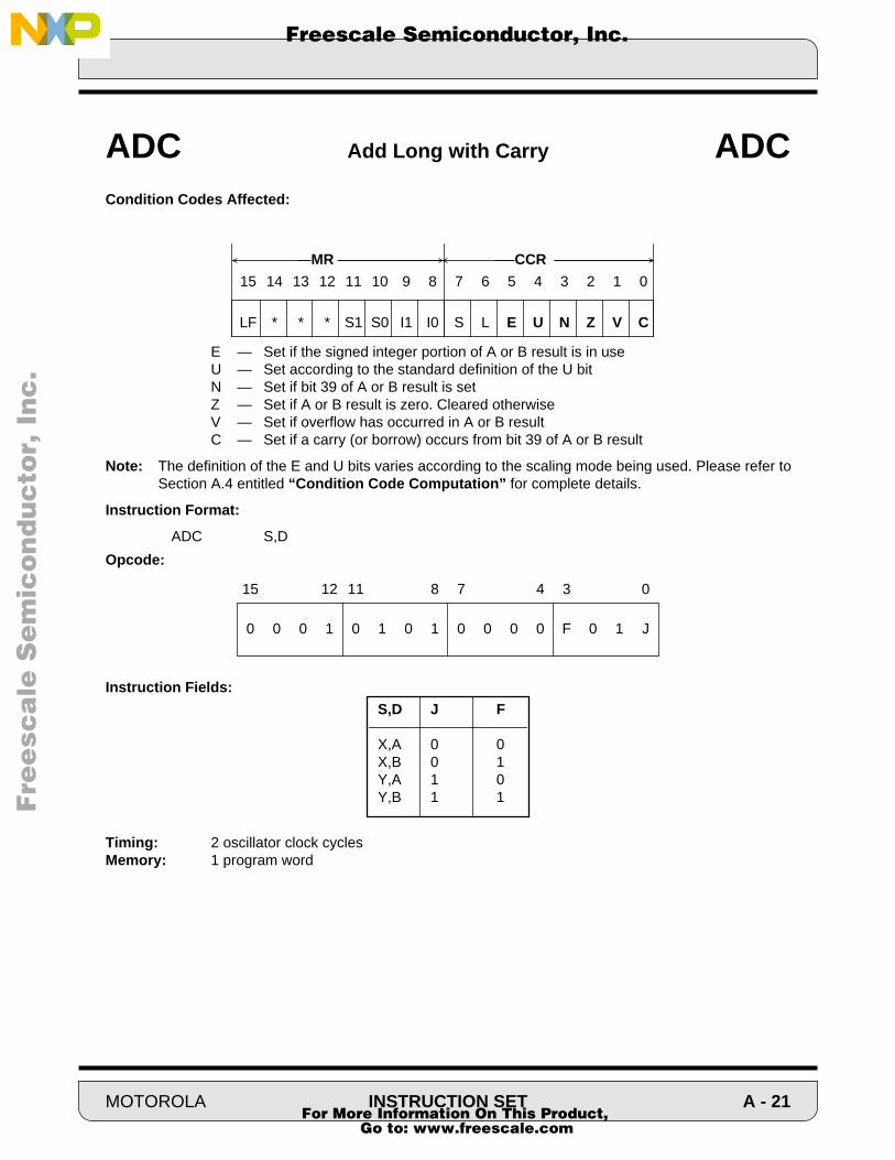
Fre
esc
ale
Se
mic
on
du
cto
r, I
Freescale Semiconductor, Inc.n
c..
.
Condition Codes Affected:
E — Set if the signed integer portion of A or B result is in useU — Set according to the standard definition of the U bitN — Set if bit 39 of A or B result is setZ — Set if A or B result is zero. Cleared otherwiseV — Set if overflow has occurred in A or B resultC — Set if a carry (or borrow) occurs from bit 39 of A or B result
Note: The definition of the E and U bits varies according to the scaling mode being used. Please refer toSection A.4 entitled “Condition Code Computation” for complete details.
Instruction Format:
ADC S,D
Opcode:
Instruction Fields:
Timing: 2 oscillator clock cyclesMemory: 1 program word
ADC Add Long with Carry ADC
15 14 13 12 11 10 9 8 7 6 5 4 3 2 1 0
LF * * * S1 S0 I1 I0 S L E U N Z V C
CCRMR
0 0 0 1 0 1 0 1 0 0 0 0 F 0 1 J
15 12 11 8 7 4 3 0
S,D J F
X,A 0 0X,B 0 1Y,A 1 0Y,B 1 1
MOTOROLA INSTRUCTION SET A - 21 For More Information On This Product,
Go to: www.freescale.com

Fre
esc
ale
Se
mic
on
du
cto
r, I
Freescale Semiconductor, Inc.n
c..
.
Operation: Assembler Syntax:
S + D → D (parallel move) ADD S,D (parallel move)
Description: Add the source operand S to the destination operand D and store the result in the destina-tion accumulator. Words (16 bits), long words (32 bits) and accumulators (40 bits) may beadded to the destination accumulator.
Note: The carry bit is set correctly using word or long word source operands if the extension register ofthe destination accumulator (A2 or B2) is the sign extension of bit 31 of the destination accumulator(A or B). The carry bit is always set correctly using accumulator source operands.
Example:
:ADD X0,A X:(R0)+,X0 X:(R3)+,X1 ;16-bit add, update X1,X0,R0,R3
::
ADD X0,A A,X:(R1)+ ;16-bit add, save accumulator:
Explanation of Example: Prior to execution, the16-bit X0 register contains the value $FFFF and the 40-bit A accumulator contains the value $00:0100:0000. The ADD instruction automatically ap-pends the 16-bit value in the X0 register with 16 LS zeros, sign extends the resulting 32-bitlong word to 40 bits and adds the result to the 40- bit A accumulator. Thus, 16-bit operandsare added to the MSP portion of A or B (A1 or B1) because all arithmetic instructions as-sume a fractional, two’s complement data representation. Note that 16-bit operands can beadded to the LSP portion of A or B (A0 or B0) by loading the 16-bit operand into X0 or Y0,forming a 32-bit word by loading X1 or Y1 with the sign extension of X0 or Y0 and executingan ADD X,A or ADD Y,A instruction.
ADD Add ADD
After Last Execution
00 00FF 0000
A2 A1 A0
Before Last Execution
00 0100 0000
A2 A1 A0
FFFF
X0
FFFF
X0
A - 22 INSTRUCTION SET MOTOROLA For More Information On This Product,
Go to: www.freescale.com
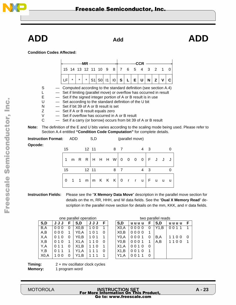
Fre
esc
ale
Se
mic
on
du
cto
r, I
Freescale Semiconductor, Inc.n
c..
.
Condition Codes Affected:
S — Computed according to the standard definition (see section A.4)L — Set if limiting (parallel move) or overflow has occurred in resultE — Set if the signed integer portion of A or B result is in useU — Set according to the standard definition of the U bitN — Set if bit 39 of A or B result is setZ — Set if A or B result equals zeroV — Set if overflow has occurred in A or B resultC — Set if a carry (or borrow) occurs from bit 39 of A or B result
Note: The definition of the E and U bits varies according to the scaling mode being used. Please refer toSection A.4 entitled “Condition Code Computation” for complete details.
Instruction Format: ADD S,D (parallel move)
Opcode:
Instruction Fields: Please see the “X Memory Data Move” description in the parallel move section for details on the m, RR, HHH, and W data fields. See the “Dual X Memory Read” de-scription in the parallel move section for details on the mm, KKK, and rr data fields.
Timing: 2 + mv oscillator clock cyclesMemory: 1 program word
ADD Add ADD
15 14 13 12 11 10 9 8 7 6 5 4 3 2 1 0
LF * * * S1 S0 I1 I0 S L E U N Z V C
CCRMR
1 m R R H H H W 0 0 0 0 F J J J
15 12 11 8 7 4 3 0
0 1 1 m m K K K 0 r r u F u u u
15 12 11 8 7 4 3 0
S,D J J J FB,A 0 0 0 0A,B 0 0 0 1X,A 0 1 0 0X,B 0 1 0 1Y,A 0 1 1 0Y,B 0 1 1 1X0,A 1 0 0 0
S,D J J J FX0,B 1 0 0 1Y0,A 1 0 1 0Y0,B 1 0 1 1X1,A 1 1 0 0X1,B 1 1 0 1Y1,A 1 1 1 0Y1,B 1 1 1 1
S,D u u u u FX0,A 0 0 0 0 0X0,B 0 0 0 0 1Y0,A 0 0 0 1 0Y0,B 0 0 0 1 1X1,A 0 0 1 0 0X1,B 0 0 1 0 1Y1,A 0 0 1 1 0
S,D u u u u FY1,B 0 0 1 1 1
B,A 1 1 0 0 0A,B 1 1 0 0 1
one parallel operation two parallel reads
MOT
OROLA INSTRUCTION SET A - 23 For More Information On This Product,Go to: www.freescale.com

Fre
esc
ale
Se
mic
on
du
cto
r, I
Freescale Semiconductor, Inc.n
c..
.
Operation: Assembler Syntax:
S•D[31:16] → D[31:16] (parallel move) AND S,D (parallel move)
where • denotes the logical AND operator
Description: Logically AND the source operand S with bits 31-16 of the destination operand D and storethe result in bits 31-16 of the destination accumulator. This instruction is a 16-bit operation.The remaining bits of the destination operand D are not affected.
Example:
AND X0,A (R2)-N2 ;AND X0 with A1, update R2 using N2:
Explanation of Example: Prior to execution, the 16-bit X0 register contains the value $FF00 and the 40-bit A accumulator contains the value $00:1234:5678. The AND X0,A instruction logicallyAND’s the 16-bit value in the X0 register with bits 31-16 of the A accumulator (A1) andstores the 40-bit result in the A accumulator.
Condition Codes Affected:
S — Computed according to the standard definition (see section A.4)L — Set if data limiting has occurred during parallel moveN — Set if bit 31 of A or B result is setZ — Set if bits 31-16 of A or B result are zeroV — Always cleared
AND Logical AND AND
After Execution
00 1200 5678
A2 A1 A0
Before Execution
00 1234 5678
A2 A1 A0
FF00
X0
FF00
X0
15 14 13 12 11 10 9 8 7 6 5 4 3 2 1 0
LF * * * S1 S0 I1 I0 S L E U N Z V C
CCRMR
A - 24 INSTRUCTION SET MOTOROLA For More Information On This Product,
Go to: www.freescale.com
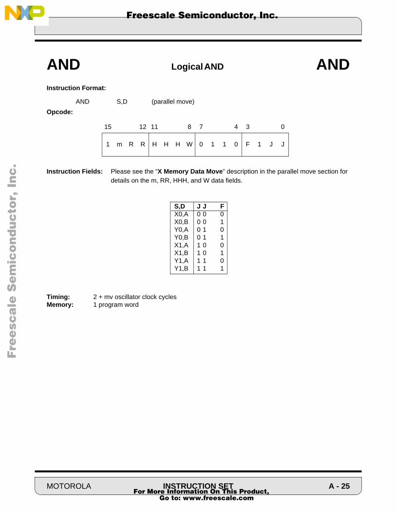
F
ree
sca
le S
em
ico
nd
uc
tor,
I
Freescale Semiconductor, Inc.n
c..
.
Instruction Format:
AND S,D (parallel move)
Opcode:
Instruction Fields: Please see the “X Memory Data Move” description in the parallel move section for details on the m, RR, HHH, and W data fields.
Timing: 2 + mv oscillator clock cyclesMemory: 1 program word
AND Logical AND AND
1 m R R H H H W 0 1 1 0 F 1 J J
15 12 11 8 7 4 3 0
S,D J J FX0,A 0 0 0X0,B 0 0 1Y0,A 0 1 0Y0,B 0 1 1X1,A 1 0 0X1,B 1 0 1Y1,A 1 1 0Y1,B 1 1 1
MOTOROLA INSTRUCTION SET A - 25 For More Information On This Product,
Go to: www.freescale.com

F
ree
sca
le S
em
ico
nd
uc
tor,
I
Freescale Semiconductor, Inc.n
c..
.
Operation: Assembler Syntax:
#xx • D → D (no parallel move) AND(I) #xx,D
where • denotes the logical AND operator
Description: Logically AND the 8-bit immediate operand (#xx) with the contents of the destination controlregister D and store the result in the destination control register. The condition codes areaffected only when the condition code register (CCR) is specified as the destination oper-and.
Restrictions: The ANDI #xx,MR instruction cannot be used immediately before an ENDDO or RTI in-struction and cannot be one of the last three instructions in a DO loop (at LA-2, LA-1 or LA).
The ANDI #xx,CCR instruction cannot be used immediately before an RTI instruction.
Example::
AND #$FE,CCR ;clear carry bit C in cond. code register:
Explanation of Example: Prior to execution, the 8-bit condition code register (CCR) contains the value$31. The AND #$FE,CCR instruction logically AND’s the immediate 8-bit value $FE withthe contents of the condition code register and stores the result in the condition code reg-ister.
ANDI AND Immediate ANDI
SR Before Execution
xx31
MR:CCR
SR After Execution
xx30
MR:CCR
A - 26 INSTRUCTION SET MOTOROLA For More Information On This Product,
Go to: www.freescale.com

F
ree
sca
le S
em
ico
nd
uc
tor,
I
Freescale Semiconductor, Inc.n
c..
.
Condition Codes Affected:
For CCR operand:S — Cleared if bit 7 of the immediate operand is clearedL — Cleared if bit 6 of the immediate operand is clearedE — Cleared if bit 5 of the immediate operand is clearedU — Cleared if bit 4 of the immediate operand is clearedN — Cleared if bit 3 of the immediate operand is clearedZ — Cleared if bit 2 of the immediate operand is clearedV — Cleared if bit 1 of the immediate operand is clearedC — Cleared if bit 0 of the immediate operand is cleared
For MR and OMR operands:The condition codes are not affected using these operands
Instruction Format:
AND(I) #xx,D
Opcode:
Instruction Fields:: #xx = 8-bit Immediate Short Data — i i i i i i i i
Timing: 2 oscillator clock cyclesMemory: 1 program word
ANDI AND Immediate ANDI
15 14 13 12 11 10 9 8 7 6 5 4 3 2 1 0
LF * * * S1 S0 I1 I0 S L E U N Z V C
CCRMR
0 0 0 1 1 E E 0 i i i i i i i i
15 12 11 8 7 4 3 0
D E EMR 0 1CCR 1 1OMR 1 0
MOTOROLA INSTRUCTION SET A - 27 For More Information On This Product,
Go to: www.freescale.com
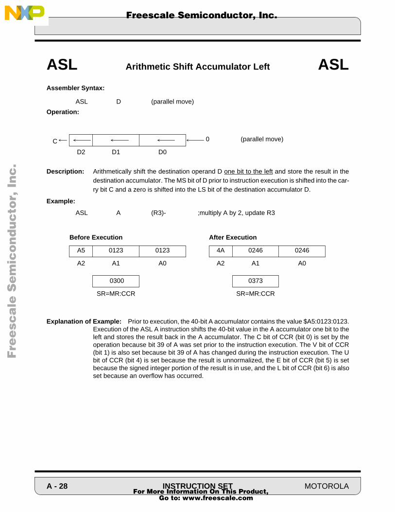
F
ree
sca
le S
em
ico
nd
uc
tor,
I
Freescale Semiconductor, Inc.n
c..
.
Assembler Syntax:
ASL D (parallel move)
Operation:
Description: Arithmetically shift the destination operand D one bit to the left and store the result in thedestination accumulator. The MS bit of D prior to instruction execution is shifted into the car-ry bit C and a zero is shifted into the LS bit of the destination accumulator D.
Example:
ASL A (R3)- ;multiply A by 2, update R3
Explanation of Example: Prior to execution, the 40-bit A accumulator contains the value $A5:0123:0123.Execution of the ASL A instruction shifts the 40-bit value in the A accumulator one bit to theleft and stores the result back in the A accumulator. The C bit of CCR (bit 0) is set by theoperation because bit 39 of A was set prior to the instruction execution. The V bit of CCR(bit 1) is also set because bit 39 of A has changed during the instruction execution. The Ubit of CCR (bit 4) is set because the result is unnormalized, the E bit of CCR (bit 5) is setbecause the signed integer portion of the result is in use, and the L bit of CCR (bit 6) is alsoset because an overflow has occurred.
ASL Arithmetic Shift Accumulator Left ASL
0 (parallel move)
D2 D1 D0
C
0300
SR=MR:CCR
0373
SR=MR:CCR
After Execution
4A 0246 0246
A2 A1 A0
Before Execution
A5 0123 0123
A2 A1 A0
A - 28 INSTRUCTION SET MOTOROLA For More Information On This Product,
Go to: www.freescale.com

F
ree
sca
le S
em
ico
nd
uc
tor,
I
Freescale Semiconductor, Inc.n
c..
.
Condition Codes Affected:
S — Computed according to the standard definition (see section A.4)L — Set if limiting (parallel move) or overflow has occurred in resultE — Set if the signed integer portion of A or B result is in useU — Set according to the standard definition of the U bitN — Set if bit 39 of A or B result is setZ — Set if A or B result equals zeroV — Set if bit 39 of A or B result is changed due to left shiftC — Set if bit 39 of A or B was set prior to instruction execution
Note: The definition of the E and U bits varies according to the scaling mode being used. Please refer toSection A.4 entitled “Condition Code Computation” for complete details.
Instruction Format:
ASL D (parallel move)
Opcode:
Instruction Fields: Please see the “X Memory Data Move” description in the parallel move section for details on the m, RR, HHH, and W data fields.
Timing: 2 + mv oscillator clock cyclesMemory: 1 program word
ASL Arithmetic Shift Accumulator Left ASL
15 14 13 12 11 10 9 8 7 6 5 4 3 2 1 0
LF * * * S1 S0 I1 I0 S L E U N Z V C
CCRMR
1 m R R H H H W 0 0 1 1 F 0 0 1
15 12 11 8 7 4 3 0
D F
A 0B 1
MOTOROLA INSTRUCTION SET A - 29 For More Information On This Product,
Go to: www.freescale.com

F
ree
sca
le S
em
ico
nd
uc
tor,
I
Freescale Semiconductor, Inc.n
c..
.
Assembler Syntax:
ASL4 D (no parallel move)
Operation:
Description: Arithmetically shift the destination operand D four bits to the left and store the result in thedestination accumulator. Bit 36 of D (bit 4 of D2) prior to instruction execution is shifted intothe carry bit C and zeros are shifted into the four LS bits of the destination accumulator D.
Example:
ASL4 A ;scaled four times to the left
Explanation of Example: Prior to execution, the 40-bit A accumulator contains the value $B5:0123:0123.Execution of the ASL4 A instruction shifts the 40-bit value in the A accumulator four bits tothe left and stores the result ($50:1230:1230) back in the A accumulator.The C bit of CCR(bit 0) is set by the operation because bit 36 of A was set prior to the instruction execution.The V bit of CCR (bit 1) is also set because bit 39 of A has changed during the instructionexecution. The U bit of CCR (bit 4) is set because bit 31 and 30 of the result are equal, theE bit of CCR (bit 5) is set because the signed integer portion of the result is in use, and theL bit of CCR (bit 6) is also set because an overflow has occurred.
Warning: The saturation mode is ALWAYS disabled during execution of ASL4, even when the satu-ration bit (SA) of the OMR is set.ASL4 A (or B) can be followed by a MOVE A,A (or B,B) for proper operation when the sat-uration mode is turned on. However, the “V” bit of the status register will never be set bythe saturation of the accumulator during the MOVE A,A (of B,B). Only the “L” bit will thenbe set. If the “V” bit needs to be tested by the user program, ASL4 has to be substituted bya repetition of four ASLs.Refer to Sections 5.3 and 5.8 for more details.
ASL4 4-bit Arithmetic Shift Accumulator Left ASL4
0
D2 D1 D0
C36
0300
SR=MR:CCR
0373
SR=MR:CCR
After Execution
50 1230 1230
A2 A1 A0
Before Execution
B5 0123 0123
A2 A1 A0
A - 30 INSTRUCTION SET MOTOROLA For More Information On This Product,
Go to: www.freescale.com
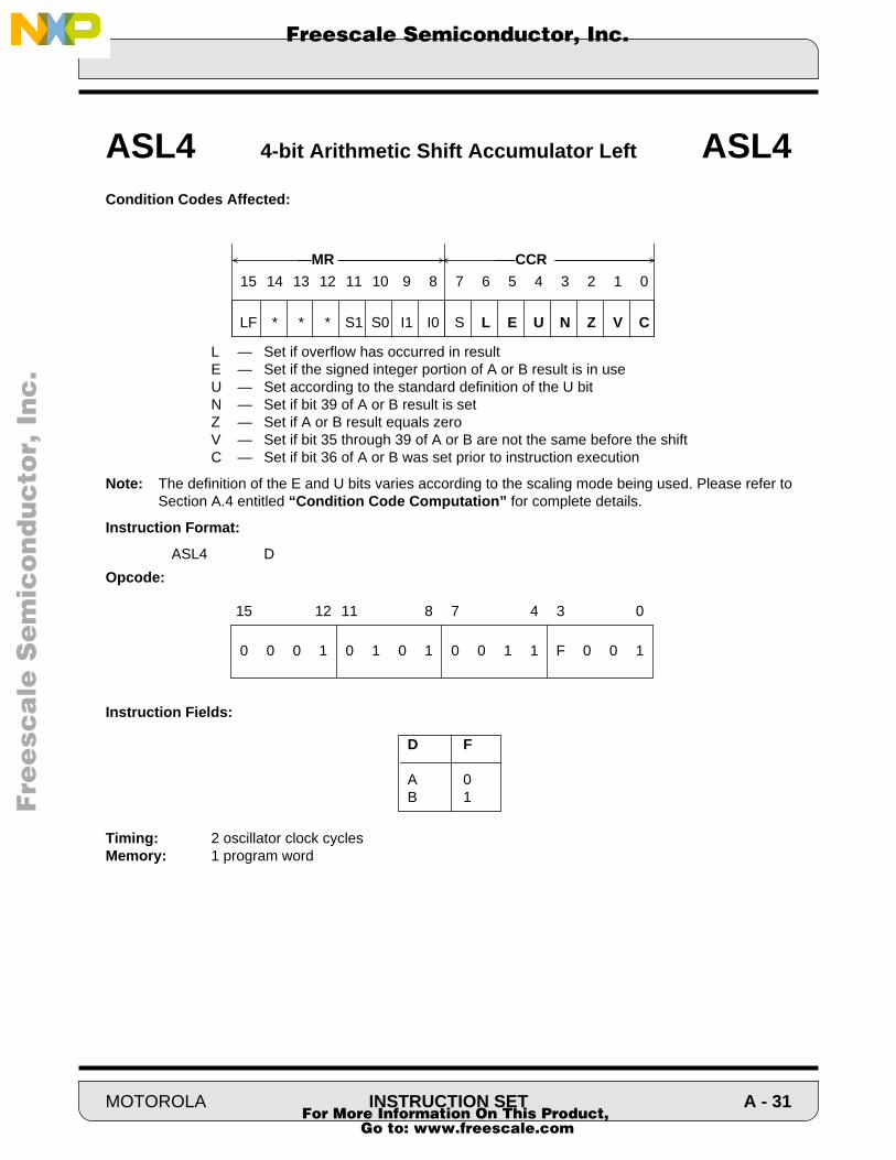
F
ree
sca
le S
em
ico
nd
uc
tor,
I
Freescale Semiconductor, Inc.n
c..
.
Condition Codes Affected:
L — Set if overflow has occurred in resultE — Set if the signed integer portion of A or B result is in useU — Set according to the standard definition of the U bitN — Set if bit 39 of A or B result is setZ — Set if A or B result equals zeroV — Set if bit 35 through 39 of A or B are not the same before the shiftC — Set if bit 36 of A or B was set prior to instruction execution
Note: The definition of the E and U bits varies according to the scaling mode being used. Please refer toSection A.4 entitled “Condition Code Computation” for complete details.
Instruction Format:
ASL4 D
Opcode:
Instruction Fields:
Timing: 2 oscillator clock cyclesMemory: 1 program word
ASL4 4-bit Arithmetic Shift Accumulator Left ASL4
15 14 13 12 11 10 9 8 7 6 5 4 3 2 1 0
LF * * * S1 S0 I1 I0 S L E U N Z V C
CCRMR
0 0 0 1 0 1 0 1 0 0 1 1 F 0 0 1
15 12 11 8 7 4 3 0
D F
A 0B 1
MOTOROLA INSTRUCTION SET A - 31 For More Information On This Product,
Go to: www.freescale.com

F
ree
sca
le S
em
ico
nd
uc
tor,
I
Freescale Semiconductor, Inc.n
c..
.
Assembler Syntax:
ASR D (parallel move)
Operation:
Description: Arithmetically shift the destination operand D one bit to the right and store the result in thedestination accumulator. The LS bit of D prior to instruction execution is shifted into the car-ry bit C and the MS bit of D is held constant.
Example:
:ASR B X:-(R3),R3 ;divide B by 2 (unless B is -1), update R3, load R3
Explanation of Example: Prior to execution, the 40-bit B accumulator contains the value$A8:A864:A865. Execution of the ASR B instruction shifts the 40-bit value in the B accu-mulator one bit to the right and stores the result back in the B accumulator. The C bit ofCCR (bit 0) is set by the operation because bit 0 of A was set prior to the instruction exe-cution. The N bit of CCR (bit 3) is also set because bit 39 of the result in A is set. The E bitof CCR (bit 5) is set because the signed integer portion of B is used by the result.
ASR Arithmetic Shift Accumulator Right ASR
C (parallel move)
D2 D1 D0
0300
SR=MR:CCR
0329
SR=MR:CCR
After Execution
D4 5432 5432
B2 B1 B0
Before Execution
A8 A864 A865
B2 B1 B0
A - 32 INSTRUCTION SET MOTOROLA For More Information On This Product,
Go to: www.freescale.com

F
ree
sca
le S
em
ico
nd
uc
tor,
I
Freescale Semiconductor, Inc.n
c..
.
Condition Codes Affected:
S — Computed according to the standard definition (see section A.4)L — Set if data limiting has occurred during parallel moveE — Set if the signed integer portion of A or B result is in useU — Set according to the standard definition of the U bitN — Set if bit 39 of A or B result is setZ — Set if A or B result equals zeroV — Always clearedC — Set if bit 0 of A or B was set prior to instruction execution
Note: The definition of the E and U bits varies according to the scaling mode being used. Please refer toSection A.4 entitled “Condition Code Computation” for complete details.
Instruction Format:
ASR D (parallel move)
Opcode:
Instruction Fields: Please see the “X Memory Data Move” description in the parallel move section for details on the m, RR, HHH, and W data fields.
Timing: 2 + mv oscillator clock cyclesMemory: 1 program words
ASR Arithmetic Shift Accumulator Right ASR
15 14 13 12 11 10 9 8 7 6 5 4 3 2 1 0
LF * * * S1 S0 I1 I0 S L E U N Z V C
CCRMR
1 m R R H H H W 0 0 1 1 F 0 0 0
15 12 11 8 7 4 3 0
D F
A 0B 1
MOTOROLA INSTRUCTION SET A - 33 For More Information On This Product,
Go to: www.freescale.com

F
ree
sca
le S
em
ico
nd
uc
tor,
I
Freescale Semiconductor, Inc.n
c..
.
Assembler Syntax:
ASR4 D (no parallel move)
Operation:
Description: Arithmetically shift the destination operand D four bits to the right and store the result in thedestination accumulator. Bit 3 of D prior to instruction execution is shifted into the carry bitC and the 4 MS bits of D are set to the MSB of D prior to instruction execution.
Example:
ASR4 B
Explanation of Example: Prior to execution, the 40-bit B accumulator contains the value$A8:A864:A86C. Execution of the ASR4 B instruction shifts the 40-bit value in the B accu-mulator four bit to the right and stores the result back in the B accumulator. The C bit ofCCR (bit 0) is set by the operation because bit 3 of B was set prior to the instruction exe-cution. The N bit of CCR (bit 3) is also set because bit 39 of the result in B is set. The E bitof CCR (bit 5) is set because the signed integer portion of B is used by the result.
ASR4 4-bit Arithmetic Shift Accumulator Right ASR4
C
D2 D1 D0
3
0300
SR=MR:CCR
0329
SR=MR:CCR
After Execution
FA 8A86 4A86
B2 B1 B0
Before Execution
A8 A864 A86C
B2 B1 B0
A - 34 INSTRUCTION SET MOTOROLA For More Information On This Product,
Go to: www.freescale.com

F
ree
sca
le S
em
ico
nd
uc
tor,
I
Freescale Semiconductor, Inc.n
c..
.
Condition Codes Affected:
E — Set if the signed integer portion of A or B result is in useU — Set according to the standard definition of the U bitN — Set if bit 39 of A or B result is setZ — Set if A or B result equals zeroV — Always clearedC — Set if bit 3 of A or B was set prior to instruction execution
Note: The definition of the E and U bits varies according to the scaling mode being used. Please refer toSection A.4 entitled “Condition Code Computation” for complete details.
Instruction Format:
ASR4 D
Opcode:
Instruction Fields:
Timing: 2 oscillator clock cyclesMemory: 1 program words
ASR4 4-bit Arithmetic Shift Accumulator Right ASR4
15 14 13 12 11 10 9 8 7 6 5 4 3 2 1 0
LF * * * S1 S0 I1 I0 S L E U N Z V C
CCRMR
0 0 0 1 0 1 0 1 0 0 1 1 F 0 0 0
15 12 11 8 7 4 3 0
D F
A 0B 1
MOTOROLA INSTRUCTION SET A - 35 For More Information On This Product,
Go to: www.freescale.com

F
ree
sca
le S
em
ico
nd
uc
tor,
I
Freescale Semiconductor, Inc.n
c..
.
Assembler Syntax:
ASR16 D (no parallel move)
Operation:
Description: Arithmetically shift the destination operand D 16 bits to the right and store the result in thedestination accumulator. The MS bit of D0 (bit 15 of D), prior to instruction execution, isshifted into the carry bit C and the MS bits of D are signed extended.
Example:
ASR16 A
Explanation of Example: Prior to execution, the 40-bit A accumulator contains the value$A8:A864:A864. Execution of the ASR16 A instruction shifts the 40-bit value in the A accu-mulator 16 bits to the right and stores the result back in the A accumulator. The C bit ofCCR (bit 0) is set by the operation because bit 15 of A was set prior to the instruction exe-cution. The N bit of CCR (bit 3) is also set because bit 39 of the result in A is set. The U bitof CCR (bit 4) is set because bit 31 and bit 30 of the result are equal.
ASR16 16-bit Arithmetic Shift Accumulator Right ASR16
C (no parallel move)
D2 D1 D0
15
0000
SR=MR:CCR
0019
SR=MR:CCR
After Execution
FF FFA8 A864
A2 A1 A0
Before Execution
A8 A864 A864
A2 A1 A0
A - 36 INSTRUCTION SET MOTOROLA For More Information On This Product,
Go to: www.freescale.com
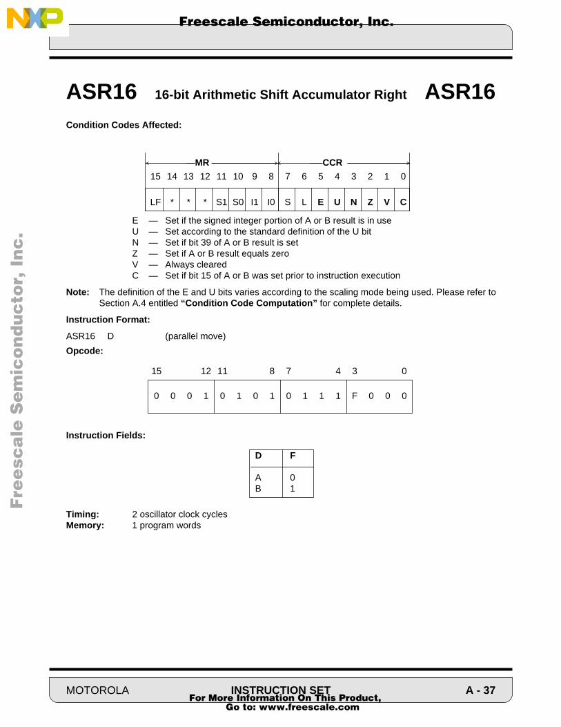
F
ree
sca
le S
em
ico
nd
uc
tor,
I
Freescale Semiconductor, Inc.n
c..
.
Condition Codes Affected:
E — Set if the signed integer portion of A or B result is in useU — Set according to the standard definition of the U bitN — Set if bit 39 of A or B result is setZ — Set if A or B result equals zeroV — Always clearedC — Set if bit 15 of A or B was set prior to instruction execution
Note: The definition of the E and U bits varies according to the scaling mode being used. Please refer toSection A.4 entitled “Condition Code Computation” for complete details.
Instruction Format:
ASR16 D (parallel move)
Opcode:
Instruction Fields:
Timing: 2 oscillator clock cyclesMemory: 1 program words
ASR16 16-bit Arithmetic Shift Accumulator Right ASR16
15 14 13 12 11 10 9 8 7 6 5 4 3 2 1 0
LF * * * S1 S0 I1 I0 S L E U N Z V C
CCRMR
0 0 0 1 0 1 0 1 0 1 1 1 F 0 0 0
15 12 11 8 7 4 3 0
D F
A 0B 1
MOTOROLA INSTRUCTION SET A - 37 For More Information On This Product,
Go to: www.freescale.com

F
ree
sca
le S
em
ico
nd
uc
tor,
I
Freescale Semiconductor, Inc.n
c..
.
Operation: Assembler Syntax:
(<bit field> of destination) → (<bit field> of destination) BFCHG #iiii,X:<aa>(<bit field> of destination) → (<bit field> of destination) BFCHG #iiii,X:<pp>(<bit field> of destination) → (<bit field> of destination) BFCHG #iiii,X:<ea>(<bit field> of destination) → (<bit field> of destination) BFCHG #iiii,D
Description: Test up to 8 bits grouped within a byte of the destination operand, complement them andstore the result in the destination memory location. The bits to be tested are selected by animmediate 16-bit hexadecimal number in which every bit set is to be tested and changed.The bits to be tested need to be located in the same byte (low byte for bits 0-7; middle bytefor bits 4-11; high byte for bits 8-15). This instruction performs a read-modify-write opera-tion on the destination memory location or register and requires two destination accesses.This instruction is very useful for performing I/O bit manipulation.
Example:
BFCHG #$0310,X:<<$FFE2 ;test and change bits 4,8,9 in I/O Port B Data Register
Explanation of Example: Prior to execution, the 16-bit X memory location X:$FFE2 (I/O Port B DataRegister) contains the value $0010. Execution of the instruction tests the state of the bits4,8,9 in X:$FFE2, does not set the carry bit C in CCR because all of these bits were not set,and then complements the bits.
Condition Codes Affected:
For destination operand SR:— Changed if specified in the field
For other destination operands:L — Set if data limiting occurred during 40-bit source moveC — Set if the all bits specified by the mask are set
Warning: Bit field instructions should always be used with a mask different from zero.
BFCHG Test Bit Field and Change BFCHG
Before Execution
X:$FFE2 0010
0000
SR=MR:CCR
After Execution
X:$FFE2 0300
0000
SR=MR:CCR
15 14 13 12 11 10 9 8 7 6 5 4 3 2 1 0
LF * * * S1 S0 I1 I0 S L E U N Z V C
CCRMR
A - 38 INSTRUCTION SET MOTOROLA For More Information On This Product,
Go to: www.freescale.com
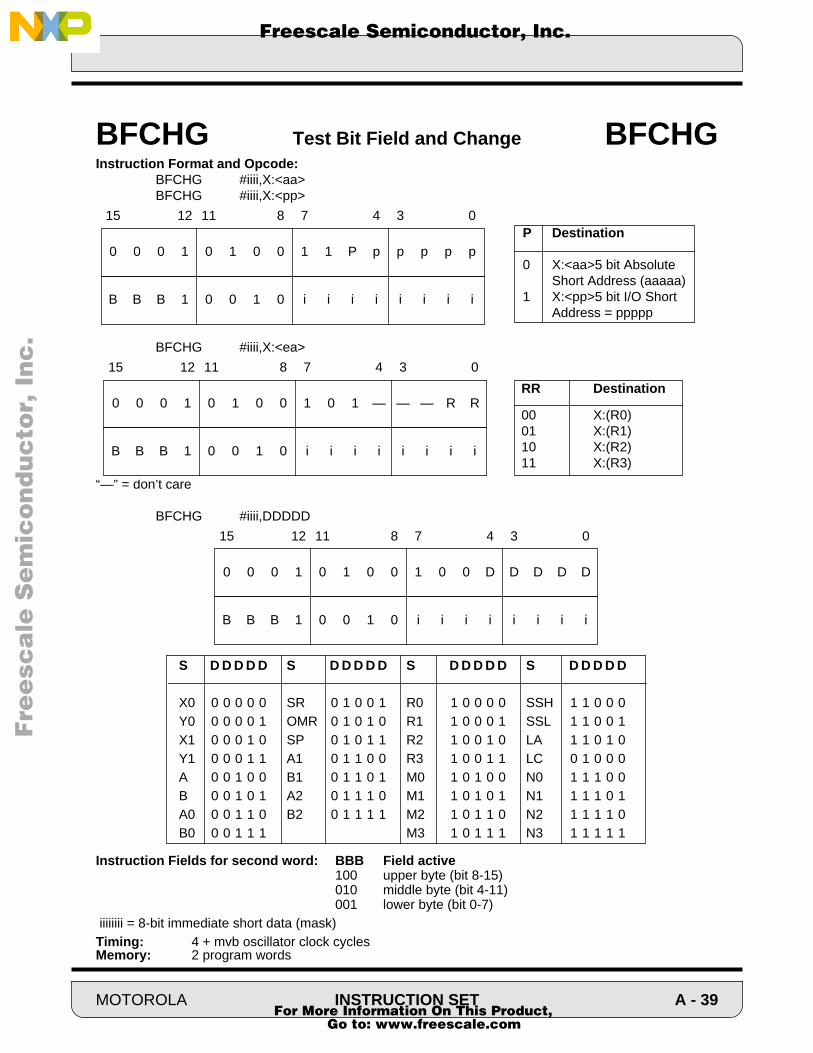
F
ree
sca
le S
em
ico
nd
uc
tor,
I
Freescale Semiconductor, Inc.n
c..
.
Instruction Format and Opcode:BFCHG #iiii,X:<aa>BFCHG #iiii,X:<pp>
BFCHG #iiii,X:<ea>
“—” = don’t care
BFCHG #iiii,DDDDD
Instruction Fields for second word: BBB Field active 100 upper byte (bit 8-15)
010 middle byte (bit 4-11)001 lower byte (bit 0-7)
iiiiiiii = 8-bit immediate short data (mask)Timing: 4 + mvb oscillator clock cyclesMemory: 2 program words
BFCHG Test Bit Field and Change BFCHG
B B B 1 0 0 1 0 i i i i i i i i
0 0 0 1 0 1 0 0 1 1 P p p p p p
15 12 11 8 7 4 3 0P Destination
0 X:<aa>5 bit Absolute Short Address (aaaaa)1 X:<pp>5 bit I/O Short
Address = ppppp
RR Destination
00 X:(R0)01 X:(R1)10 X:(R2)11 X:(R3)
B B B 1 0 0 1 0 i i i i i i i i
0 0 0 1 0 1 0 0 1 0 1 — — — R R
15 12 11 8 7 4 3 0
B B B 1 0 0 1 0 i i i i i i i i
0 0 0 1 0 1 0 0 1 0 0 D D D D D
15 12 11 8 7 4 3 0
S D D D D D
X0 0 0 0 0 0Y0 0 0 0 0 1X1 0 0 0 1 0Y1 0 0 0 1 1A 0 0 1 0 0B 0 0 1 0 1A0 0 0 1 1 0B0 0 0 1 1 1
S D D D D D
SR 0 1 0 0 1OMR 0 1 0 1 0SP 0 1 0 1 1A1 0 1 1 0 0B1 0 1 1 0 1A2 0 1 1 1 0B2 0 1 1 1 1
S D D D D D
R0 1 0 0 0 0R1 1 0 0 0 1R2 1 0 0 1 0R3 1 0 0 1 1M0 1 0 1 0 0M1 1 0 1 0 1M2 1 0 1 1 0M3 1 0 1 1 1
S D D D D D
SSH 1 1 0 0 0SSL 1 1 0 0 1LA 1 1 0 1 0LC 0 1 0 0 0N0 1 1 1 0 0N1 1 1 1 0 1N2 1 1 1 1 0N3 1 1 1 1 1
MOTOROLA INSTRUCTION SET A - 39 For More Information On This Product,
Go to: www.freescale.com

F
ree
sca
le S
em
ico
nd
uc
tor,
I
Freescale Semiconductor, Inc.n
c..
.
Operation: Assembler Syntax:
0 → (<bit field> of destination) BFCLR #iiii,X:<aa>0 → (<bit field> of destination) BFCLR #iiii,X:<pp>0 → (<bit field> of destination) BFCLR #iiii,X:<ea>0 → (<bit field> of destination) BFCLR #iiii,D
Description: Clear up to 8 bits grouped within a byte of the destination operand and store the result inthe destination memory location. The bits to be cleared are selected by an immediate 16-bit hexadecimal number in which every bit set is to be cleared. The bits to be cleared needto be located in the same byte (low byte for bits 0-7; middle byte for bits 4-11; high byte forbits 8-15). This instruction performs a read-modify-write operation on the destination mem-ory location or register and requires two destination accesses. This instruction is very use-ful for performing I/O bit manipulation.
Example:BFCLR #$0310,X:<<$FFE2 ;test and clear bits 4,8,9 in I/O Port B Data Register
Explanation of Example: Prior to execution, the 16-bit X memory location X:$FFE2 (I/O Port B DataRegister) contains the value $7F95. Execution of the instruction tests the state of the bits4,8,9 in X:$FFE2, clear the carry bit C in CCR because not all these bits were set, and thenclears the bits.
Condition Codes Affected:
For destination operand SR:— Cleared as defined in the field and if specified in the field
For other destination operands:L — Set if data limiting occurred during 40-bit source moveC — Set if the all bits specified by the mask are set
Clear if the not all bits specified by the mask are set
Warning: Bit field instructions should always be used with a mask different from zero. If the mask iszero, the instruction essentially executes two NOPs.
BFCLR Clear Bit Field BFCLR
Before Execution
X:$FFE2 7F95
0000
SR=MR:CCR
After Execution
X:$FFE2 7C85
0000
SR=MR:CCR
15 14 13 12 11 10 9 8 7 6 5 4 3 2 1 0
LF * * * S1 S0 I1 I0 S L E U N Z V C
CCRMR
A - 40 INSTRUCTION SET MOTOROLA For More Information On This Product,
Go to: www.freescale.com

F
ree
sca
le S
em
ico
nd
uc
tor,
I
Freescale Semiconductor, Inc.n
c..
.
Instruction Format and Opcode:BFCLR #iiii,X:<aa>BFCLR #iiii,X:<pp>
BFCLR #iiii,X:<ea>
“—” = don’t care
BFCLR #iiii,DDDDD
Instruction Fields for second word: BBB Field active 100 upper byte (bit 8-15)
010 middle byte (bit 4-11)001 lower byte (bit 0-7)
iiiiiiii = 8-bit immediate short dataTiming: 4 + mvb oscillator clock cyclesMemory: 2 program words
BFCLR Clear Bit Field BFCLR
B B B 0 0 1 0 0 i i i i i i i i
0 0 0 1 0 1 0 0 1 1 P p p p p p
15 12 11 8 7 4 3 0P Destination
0 X:<aa>5 bit Absolute Short Address (aaaaa)1 X:<pp>5 bit I/O Short
Address = ppppp
RR Destination
00 X:(R0)01 X:(R1)10 X:(R2)11 X:(R3)
B B B 0 0 1 0 0 i i i i i i i i
0 0 0 1 0 1 0 0 1 0 1 — — — R R
15 12 11 8 7 4 3 0
B B B 0 0 1 0 0 i i i i i i i i
0 0 0 1 0 1 0 0 1 0 0 D D D D D
15 12 11 8 7 4 3 0
S D D D D D
X0 0 0 0 0 0Y0 0 0 0 0 1X1 0 0 0 1 0Y1 0 0 0 1 1A 0 0 1 0 0B 0 0 1 0 1A0 0 0 1 1 0B0 0 0 1 1 1
S D D D D D
SR 0 1 0 0 1OMR 0 1 0 1 0SP 0 1 0 1 1A1 0 1 1 0 0B1 0 1 1 0 1A2 0 1 1 1 0B2 0 1 1 1 1
S D D D D D
R0 1 0 0 0 0R1 1 0 0 0 1R2 1 0 0 1 0R3 1 0 0 1 1M0 1 0 1 0 0M1 1 0 1 0 1M2 1 0 1 1 0M3 1 0 1 1 1
S D D D D D
SSH 1 1 0 0 0SSL 1 1 0 0 1LA 1 1 0 1 0LC 0 1 0 0 0N0 1 1 1 0 0N1 1 1 1 0 1N2 1 1 1 1 0N3 1 1 1 1 1
MOTOROLA INSTRUCTION SET A - 41 For More Information On This Product,
Go to: www.freescale.com

F
ree
sca
le S
em
ico
nd
uc
tor,
I
Freescale Semiconductor, Inc.n
c..
.
Operation: Assembler Syntax:
1 → (<bit field> of destination) BFSET #iiii,X:<aa>1 → (<bit field> of destination) BFSET #iiii,X:<pp>1 → (<bit field> of destination) BFSET #iiii,X:<ea>1 → (<bit field> of destination) BFSET #iiii,D
Description: Set up to 8 bits grouped within a byte of the destination operand and store the result in thedestination memory location. The bits to be set are selected by an immediate 16-bit hexa-decimal number in which every bit set is to be tested and set. The bits to be set need to belocated in the same byte (low byte for bits 0-7; middle byte for bits 4-11; high byte for bits8-15). This instruction performs a read-modify-write operation on the destination memorylocation or register and requires two destination accesses. This instruction is very useful forperforming I/O bit manipulation.
Example:BFSET #$F400,X:<<$FFE2 ;test and set bits 10,12,13,14,15 in I/O Port B
;Data Register
Explanation of Example: Prior to execution, the 16-bit X memory location X:$FFE2 (I/O Port B DataRegister) contains the value $8921. Execution of the instruction tests the state of bits10,12,13,14,15 in X:$FFE2, does not set the carry bit C in CCR because all these bits werenot set, and then sets the bits.
Condition Codes Affected:
For destination operand SR:— Set as defined in the field and if specified in the field
For other destination operands:L — Set if data limiting occurred during 40-bit source moveC — Set if the all bits specified by the mask are set
Warning: Bit field instructions should always be used with a mask different from zero. If the mask iszero, the instruction essentially executes two NOPs.
BFSET Set Bit Field BFSET
Before Execution
X:$FFE2 8921
0000
SR=MR:CCR
After Execution
X:$FFE2 FD21
0000
SR=MR:CCR
15 14 13 12 11 10 9 8 7 6 5 4 3 2 1 0
LF * * * S1 S0 I1 I0 S L E U N Z V C
CCRMR
A - 42 INSTRUCTION SET MOTOROLA For More Information On This Product,
Go to: www.freescale.com

F
ree
sca
le S
em
ico
nd
uc
tor,
I
Freescale Semiconductor, Inc.n
c..
.
Instruction Format and Opcode:BFSET #iiii,X:<aa>BFSET #iiii,X:<pp>
BFSET #iiii,X:<ea>
“—” = don’t care
BFSET #iiii,DDDDD
Instruction Fields for second word: BBB Field active 100 upper byte (bit 8-15)
010 middle byte (bit 4-11)001 lower byte (bit 0-7)
iiiiiiii = 8-bit immediate short dataTiming: 4 + mvb oscillator clock cyclesMemory: 2 program words
BFSET Set Bit Field BFSET
B B B 1 1 0 0 0 i i i i i i i i
0 0 0 1 0 1 0 0 1 1 P p p p p p
15 12 11 8 7 4 3 0P Destination
0 X:<aa>5 bit Absolute Short Address (aaaaa)1 X:<pp>5 bit I/O Short
Address = ppppp
RR Destination
00 X:(R0)01 X:(R1)10 X:(R2)11 X:(R3)
B B B 1 1 0 0 0 i i i i i i i i
0 0 0 1 0 1 0 0 1 0 1 — — — R R
15 12 11 8 7 4 3 0
B B B 1 1 0 0 0 i i i i i i i i
0 0 0 1 0 1 0 0 1 0 0 D D D D D
15 12 11 8 7 4 3 0
S D D D D D
X0 0 0 0 0 0Y0 0 0 0 0 1X1 0 0 0 1 0Y1 0 0 0 1 1A 0 0 1 0 0B 0 0 1 0 1A0 0 0 1 1 0B0 0 0 1 1 1
S D D D D D
SR 0 1 0 0 1OMR 0 1 0 1 0SP 0 1 0 1 1A1 0 1 1 0 0B1 0 1 1 0 1A2 0 1 1 1 0B2 0 1 1 1 1
S D D D D D
R0 1 0 0 0 0R1 1 0 0 0 1R2 1 0 0 1 0R3 1 0 0 1 1M0 1 0 1 0 0M1 1 0 1 0 1M2 1 0 1 1 0M3 1 0 1 1 1
S D D D D D
SSH 1 1 0 0 0SSL 1 1 0 0 1LA 1 1 0 1 0LC 0 1 0 0 0N0 1 1 1 0 0N1 1 1 1 0 1N2 1 1 1 1 0N3 1 1 1 1 1
MOTOROLA INSTRUCTION SET A - 43 For More Information On This Product,
Go to: www.freescale.com
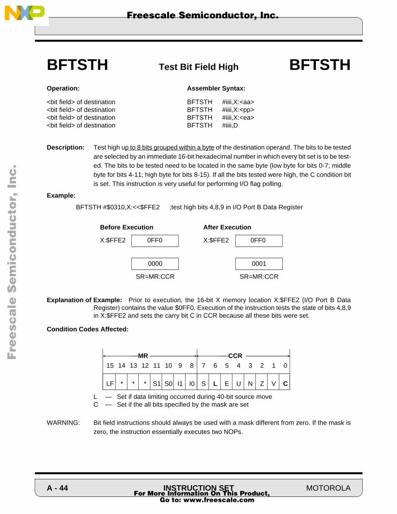
F
ree
sca
le S
em
ico
nd
uc
tor,
I
Freescale Semiconductor, Inc.n
c..
.
Operation: Assembler Syntax:
<bit field> of destination BFTSTH #iiii,X:<aa><bit field> of destination BFTSTH #iiii,X:<pp><bit field> of destination BFTSTH #iiii,X:<ea><bit field> of destination BFTSTH #iiii,D
Description: Test high up to 8 bits grouped within a byte of the destination operand. The bits to be testedare selected by an immediate 16-bit hexadecimal number in which every bit set is to be test-ed. The bits to be tested need to be located in the same byte (low byte for bits 0-7; middlebyte for bits 4-11; high byte for bits 8-15). If all the bits tested were high, the C condition bitis set. This instruction is very useful for performing I/O flag polling.
Example:
BFTSTH #$0310,X:<<$FFE2 ;test high bits 4,8,9 in I/O Port B Data Register
Explanation of Example: Prior to execution, the 16-bit X memory location X:$FFE2 (I/O Port B DataRegister) contains the value $0FF0. Execution of the instruction tests the state of bits 4,8,9in X:$FFE2 and sets the carry bit C in CCR because all these bits were set.
Condition Codes Affected:
L — Set if data limiting occurred during 40-bit source moveC — Set if the all bits specified by the mask are set
WARNING: Bit field instructions should always be used with a mask different from zero. If the mask iszero, the instruction essentially executes two NOPs.
BFTSTH Test Bit Field High BFTSTH
Before Execution
X:$FFE2 0FF0
0000
SR=MR:CCR
After Execution
X:$FFE2 0FF0
0001
SR=MR:CCR
15 14 13 12 11 10 9 8 7 6 5 4 3 2 1 0
LF * * * S1 S0 I1 I0 S L E U N Z V C
CCRMR
A - 44 INSTRUCTION SET MOTOROLA For More Information On This Product,
Go to: www.freescale.com

F
ree
sca
le S
em
ico
nd
uc
tor,
I
Freescale Semiconductor, Inc.n
c..
.
Instruction Format and Opcode:BFTSTH #iiii,X:<aa>BFTSTH #iiii,X:<pp>
BFTSTH #iiii,X:<ea>
“—” = don’t care
BFTSTH #iiii,DDDDD
Instruction Fields for second word: BBB Field active 100 upper byte (bit 8-15)
010 middle byte (bit 4-11)001 lower byte (bit 0-7)
iiiiiiii = 8-bit immediate short dataTiming: 4 + mvb oscillator clock cyclesMemory: 2 program words
BFTSTH Test Bit Field High BFTSTH
B B B 1 0 0 0 0 i i i i i i i i
0 0 0 1 0 1 0 0 0 1 P p p p p p
15 12 11 8 7 4 3 0P Destination
0 X:<aa>5 bit Absolute Short Address (aaaaa)1 X:<pp>5 bit I/O Short
Address = ppppp
RR Destination
00 X:(R0)01 X:(R1)10 X:(R2)11 X:(R3)
B B B 1 0 0 0 0 i i i i i i i i
0 0 0 1 0 1 0 0 0 0 1 — — — R R
15 12 11 8 7 4 3 0
B B B 1 0 0 0 0 i i i i i i i i
0 0 0 1 0 1 0 0 0 0 0 D D D D D
15 12 11 8 7 4 3 0
S D D D D D
X0 0 0 0 0 0Y0 0 0 0 0 1X1 0 0 0 1 0Y1 0 0 0 1 1A 0 0 1 0 0B 0 0 1 0 1A0 0 0 1 1 0B0 0 0 1 1 1
S D D D D D
SR 0 1 0 0 1OMR 0 1 0 1 0SP 0 1 0 1 1A1 0 1 1 0 0B1 0 1 1 0 1A2 0 1 1 1 0B2 0 1 1 1 1
S D D D D D
R0 1 0 0 0 0R1 1 0 0 0 1R2 1 0 0 1 0R3 1 0 0 1 1M0 1 0 1 0 0M1 1 0 1 0 1M2 1 0 1 1 0M3 1 0 1 1 1
S D D D D D
SSH 1 1 0 0 0SSL 1 1 0 0 1LA 1 1 0 1 0LC 0 1 0 0 0N0 1 1 1 0 0N1 1 1 1 0 1N2 1 1 1 1 0N3 1 1 1 1 1
MOTOROLA INSTRUCTION SET A - 45 For More Information On This Product,
Go to: www.freescale.com

F
ree
sca
le S
em
ico
nd
uc
tor,
I
Freescale Semiconductor, Inc.n
c..
.
Operation: Assembler Syntax:
<bit field> of destination BFTSTL #iiii,X:<aa><bit field> of destination BFTSTL #iiii,X:<pp><bit field> of destination BFTSTL #iiii,X:<ea><bit field> of destination BFTSTL #iiii,D
Description: Test low up to 8 bits grouped within a byte of the destination operand. The bits to be testedare selected by an immediate 16-bit hexadecimal number in which every bit set is to be test-ed. The bits to be tested need to be located in the same byte (low byte for bits 0-7; middlebyte for bits 4-11; high byte for bits 8-15). If all the bits tested were low, the C condition bitis set. This instruction is very useful for performing I/O flag polling.
Example:
BFTSTL #$0310,X:<<$FFE2 ;test low bits 4,8,9 in I/O Port B Data Register
Explanation of Example: Prior to execution, the 16-bit X memory location X:$FFE2 (I/O Port B DataRegister) contains the value $18EC. Execution of the instruction tests the state of bits 4,8,9in X:$FFE2 and sets the carry bit C in CCR because all these bits were cleared.
Condition Codes Affected:
L — Set if data limiting occurred during 40-bit source moveC — Set if the all bits specified by the mask are cleared
WARNING: Bit field instructions should always be used with a mask different from zero. If the mask iszero, the instruction essentially executes two NOPs.
BFTSTL Test Bit Field Low BFTSTL
Before Execution
X:$FFE2 18EC
0000
SR=MR:CCR
After Execution
X:$FFE2 18EC
0001
SR=MR:CCR
15 14 13 12 11 10 9 8 7 6 5 4 3 2 1 0
LF * * * S1 S0 I1 I0 S L E U N Z V C
CCRMR
A - 46 INSTRUCTION SET MOTOROLA For More Information On This Product,
Go to: www.freescale.com
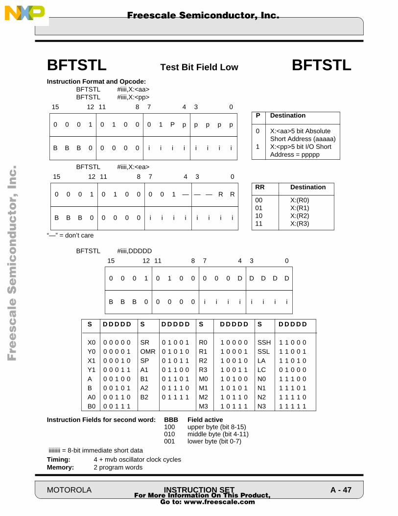
F
ree
sca
le S
em
ico
nd
uc
tor,
I
Freescale Semiconductor, Inc.n
c..
.
Instruction Format and Opcode:BFTSTL #iiii,X:<aa>BFTSTL #iiii,X:<pp>
BFTSTL #iiii,X:<ea>
“—” = don’t care
BFTSTL #iiii,DDDDD
Instruction Fields for second word: BBB Field active 100 upper byte (bit 8-15)
010 middle byte (bit 4-11)001 lower byte (bit 0-7)
iiiiiiii = 8-bit immediate short dataTiming: 4 + mvb oscillator clock cyclesMemory: 2 program words
BFTSTL Test Bit Field Low BFTSTL
B B B 0 0 0 0 0 i i i i i i i i
0 0 0 1 0 1 0 0 0 1 P p p p p p
15 12 11 8 7 4 3 0P Destination
0 X:<aa>5 bit Absolute Short Address (aaaaa)1 X:<pp>5 bit I/O Short
Address = ppppp
RR Destination
00 X:(R0)01 X:(R1)10 X:(R2)11 X:(R3)
B B B 0 0 0 0 0 i i i i i i i i
0 0 0 1 0 1 0 0 0 0 1 — — — R R
15 12 11 8 7 4 3 0
B B B 0 0 0 0 0 i i i i i i i i
0 0 0 1 0 1 0 0 0 0 0 D D D D D
15 12 11 8 7 4 3 0
S D D D D D
X0 0 0 0 0 0Y0 0 0 0 0 1X1 0 0 0 1 0Y1 0 0 0 1 1A 0 0 1 0 0B 0 0 1 0 1A0 0 0 1 1 0B0 0 0 1 1 1
S D D D D D
SR 0 1 0 0 1OMR 0 1 0 1 0SP 0 1 0 1 1A1 0 1 1 0 0B1 0 1 1 0 1A2 0 1 1 1 0B2 0 1 1 1 1
S D D D D D
R0 1 0 0 0 0R1 1 0 0 0 1R2 1 0 0 1 0R3 1 0 0 1 1M0 1 0 1 0 0M1 1 0 1 0 1M2 1 0 1 1 0M3 1 0 1 1 1
S D D D D D
SSH 1 1 0 0 0SSL 1 1 0 0 1LA 1 1 0 1 0LC 0 1 0 0 0N0 1 1 1 0 0N1 1 1 1 0 1N2 1 1 1 1 0N3 1 1 1 1 1
MOTOROLA INSTRUCTION SET A - 47 For More Information On This Product,
Go to: www.freescale.com

F
ree
sca
le S
em
ico
nd
uc
tor,
I
Freescale Semiconductor, Inc.n
c..
.
Operation: Assembler Syntax:
If cc, then PC+label → PC Bcc xxxxelse PC+1 → PC Bcc ee
If cc, then PC+Rn → PC Bcc Rnelse PC+1 → PC
Description: If the specified condition is true, program execution continues at location PC+displace-ment. The PC contains the address of the next instruction. If the specified condition is false,the program counter (PC) is incremented and program execution continues sequentially.Short displacement (6 bit signed value), long displacement (16 bit signed value) and ad-dress register PC relative addressing modes may be used. The 6-bit data is signed extend-ed to form the effective address.
The term “cc” may specify the following conditions:
where: U denotes the logical complement of U,+ denotes the logical OR operator,• denotes the logical AND operator,⊕ denotes the logical Exclusive OR operator
Restrictions: — A Bcc instruction used within a DO loop cannot begin at the address LA withinthat DO loop.
— A Bcc instruction cannot be repeated using the REP instruction.
— Not allowed between addresses P:$0 and P:$40.Example:
BNN R2 ;jump to P:(PC+R2) if not normalized
Explanation of Example: In this example, program execution is transferred to the address P:(PC+R2) ifthe result is not normalized. If the specified condition is not true, no jump is taken and theprogram counter is incremented by one.
Bcc Branch Conditionally Bcc
“cc” Mnemonic Condition
CC (HS) — carry clear (higher or same) C=0CS (LO) — carry set(lower) C=1EC — extension clear E=0EQ — equal Z=1ES — extension set E=1GE — greater than or equal N ⊕ V=0GT — greater than Z+(N ⊕ V)=0LC — limit clear L=0LE — less than or equal Z+(N ⊕ V)=1LS — limit set L=1LT — less than N ⊕ V=1MI — minus N=1NE — not equal Z=0NR — normalized Z+(U•E)=1PL — plus N=0NN — not normalized Z+(U•E)=0
A - 48 INSTRUCTION SET MOTOROLA For More Information On This Product,
Go to: www.freescale.com
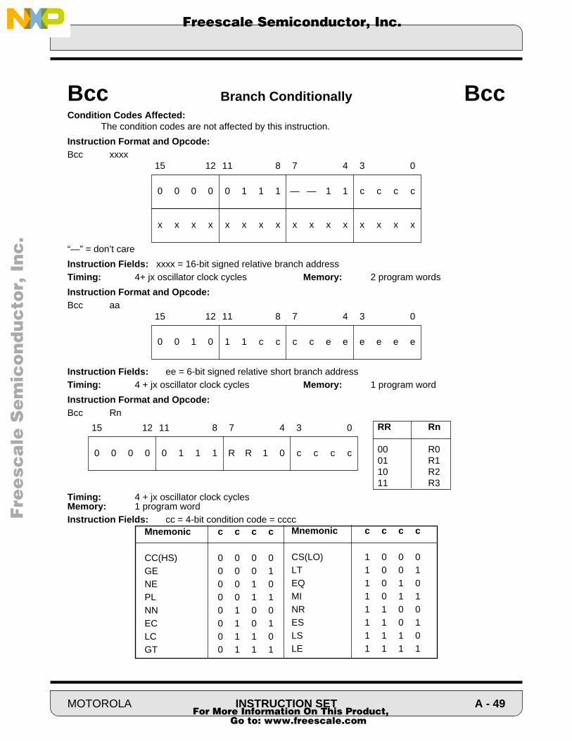
F
ree
sca
le S
em
ico
nd
uc
tor,
I
Freescale Semiconductor, Inc.n
c..
.
Condition Codes Affected:The condition codes are not affected by this instruction.
Instruction Format and Opcode:Bcc xxxx
“—” = don’t care
Instruction Fields: xxxx = 16-bit signed relative branch addressTiming: 4+ jx oscillator clock cycles Memory: 2 program words
Instruction Format and Opcode:Bcc aa
Instruction Fields: ee = 6-bit signed relative short branch addressTiming: 4 + jx oscillator clock cycles Memory: 1 program word
Instruction Format and Opcode:Bcc Rn
Timing: 4 + jx oscillator clock cyclesMemory: 1 program wordInstruction Fields: cc = 4-bit condition code = cccc
Bcc Branch Conditionally Bcc
x x x x x x x x x x x x x x x x
0 0 0 0 0 1 1 1 — — 1 1 c c c c
15 12 11 8 7 4 3 0
0 0 1 0 1 1 c c c c e e e e e e
15 12 11 8 7 4 3 0
0 0 0 0 0 1 1 1 R R 1 0 c c c c
15 12 11 8 7 4 3 0 RR Rn
00 R001 R110 R211 R3
Mnemonic c c c c
CC(HS) 0 0 0 0GE 0 0 0 1NE 0 0 1 0PL 0 0 1 1NN 0 1 0 0EC 0 1 0 1LC 0 1 1 0GT 0 1 1 1
Mnemonic c c c c
CS(LO) 1 0 0 0LT 1 0 0 1EQ 1 0 1 0MI 1 0 1 1NR 1 1 0 0ES 1 1 0 1LS 1 1 1 0LE 1 1 1 1
MOTOROLA INSTRUCTION SET A - 49 For More Information On This Product,
Go to: www.freescale.com
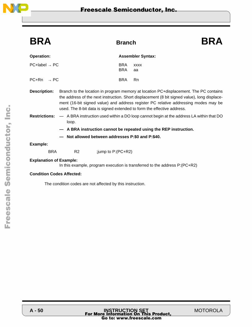
F
ree
sca
le S
em
ico
nd
uc
tor,
I
Freescale Semiconductor, Inc.n
c..
.
Operation: Assembler Syntax:
PC+label → PC BRA xxxxBRA aa
PC+Rn → PC BRA Rn
Description: Branch to the location in program memory at location PC+displacement. The PC containsthe address of the next instruction. Short displacement (8 bit signed value), long displace-ment (16-bit signed value) and address register PC relative addressing modes may beused. The 8-bit data is signed extended to form the effective address.
Restrictions: — A BRA instruction used within a DO loop cannot begin at the address LA within that DOloop.
— A BRA instruction cannot be repeated using the REP instruction.
— Not allowed between addresses P:$0 and P:$40.
Example:
BRA R2 ;jump to P:(PC+R2)
Explanation of Example:In this example, program execution is transferred to the address P:(PC+R2)
Condition Codes Affected:
The condition codes are not affected by this instruction.
BRA Branch BRA
A - 50 INSTRUCTION SET MOTOROLA For More Information On This Product,
Go to: www.freescale.com
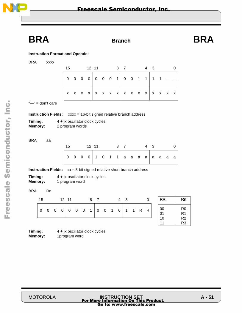
F
ree
sca
le S
em
ico
nd
uc
tor,
I
Freescale Semiconductor, Inc.n
c..
.
Instruction Format and Opcode:
BRA xxxx
“—” = don’t care
Instruction Fields: xxxx = 16-bit signed relative branch address
Timing: 4 + jx oscillator clock cyclesMemory: 2 program words
BRA aa
Instruction Fields: aa = 8-bit signed relative short branch address
Timing: 4 + jx oscillator clock cyclesMemory: 1 program word
BRA Rn
Timing: 4 + jx oscillator clock cyclesMemory: 1program word
BRA Branch BRA
x x x x x x x x x x x x x x x x
0 0 0 0 0 0 0 1 0 0 1 1 1 1 — —
15 12 11 8 7 4 3 0
0 0 0 0 1 0 1 1 a a a a a a a a
15 12 11 8 7 4 3 0
0 0 0 0 0 0 0 1 0 0 1 0 1 1 R R
15 12 11 8 7 4 3 0 RR Rn
00 R001 R110 R211 R3
MOTOROLA INSTRUCTION SET A - 51 For More Information On This Product,
Go to: www.freescale.com
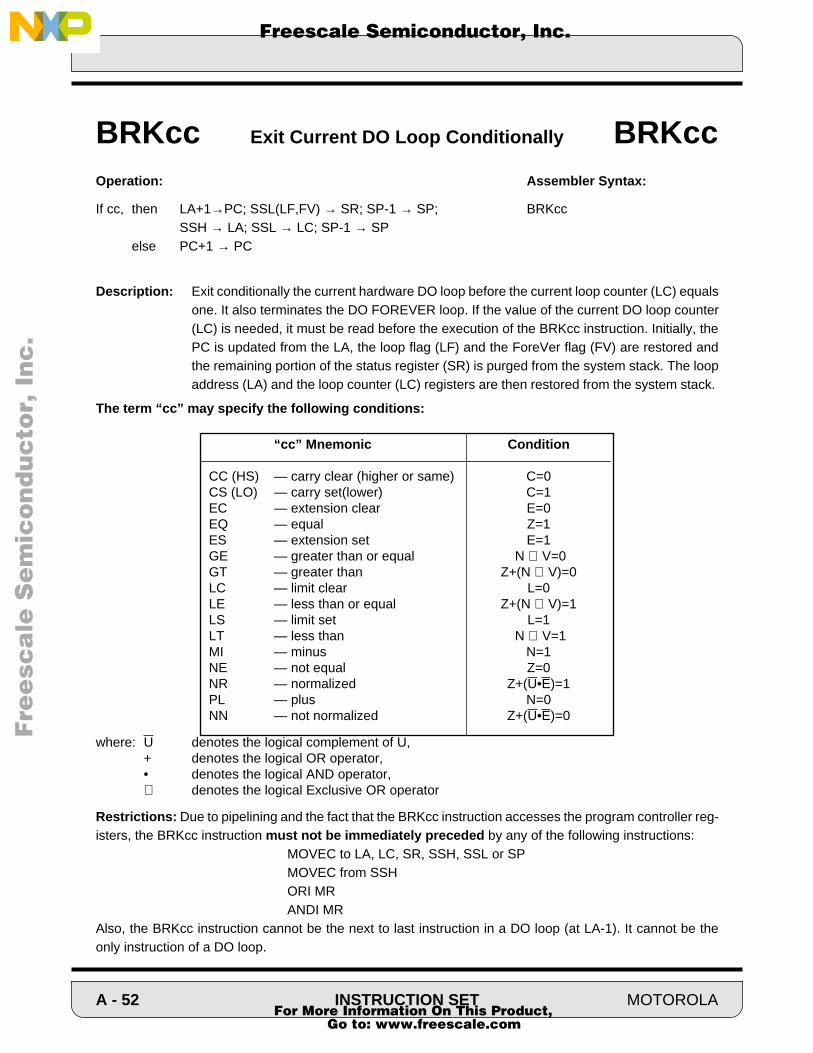
F
ree
sca
le S
em
ico
nd
uc
tor,
I
Freescale Semiconductor, Inc.n
c..
.
Operation: Assembler Syntax:
If cc, then LA+1→PC; SSL(LF,FV) → SR; SP-1 → SP; BRKccSSH → LA; SSL → LC; SP-1 → SP
else PC+1 → PC
Description: Exit conditionally the current hardware DO loop before the current loop counter (LC) equalsone. It also terminates the DO FOREVER loop. If the value of the current DO loop counter(LC) is needed, it must be read before the execution of the BRKcc instruction. Initially, thePC is updated from the LA, the loop flag (LF) and the ForeVer flag (FV) are restored andthe remaining portion of the status register (SR) is purged from the system stack. The loopaddress (LA) and the loop counter (LC) registers are then restored from the system stack.
The term “cc” may specify the following conditions:
where: U denotes the logical complement of U,+ denotes the logical OR operator,• denotes the logical AND operator,⊕ denotes the logical Exclusive OR operator
Restrictions: Due to pipelining and the fact that the BRKcc instruction accesses the program controller reg-isters, the BRKcc instruction must not be immediately preceded by any of the following instructions:
MOVEC to LA, LC, SR, SSH, SSL or SPMOVEC from SSHORI MRANDI MR
Also, the BRKcc instruction cannot be the next to last instruction in a DO loop (at LA-1). It cannot be theonly instruction of a DO loop.
BRKcc Exit Current DO Loop Conditionally BRKcc
“cc” Mnemonic Condition
CC (HS) — carry clear (higher or same) C=0CS (LO) — carry set(lower) C=1EC — extension clear E=0EQ — equal Z=1ES — extension set E=1GE — greater than or equal N ⊕ V=0GT — greater than Z+(N ⊕ V)=0LC — limit clear L=0LE — less than or equal Z+(N ⊕ V)=1LS — limit set L=1LT — less than N ⊕ V=1MI — minus N=1NE — not equal Z=0NR — normalized Z+(U•E)=1PL — plus N=0NN — not normalized Z+(U•E)=0
A - 52 INSTRUCTION SET MOTOROLA For More Information On This Product,
Go to: www.freescale.com

Fre
esc
ale
Se
mic
on
du
cto
r, I
Freescale Semiconductor, Inc.n
c..
.
Example:
DO Y0,END_LP ;exec. loop ending at END_LP (Y0) times:
MOVEC LC,A ;get current value of loop counter (LC)CMP Y1,A ;compare loop counter with value in Y1BRKNE ;go to first instruction after Do loop if LC not equal to Y1
: ;: ;: ;(last instruction word in DO loop)
END_LP MOVE #$123456,X1 ;(first instruction AFTER DO loop)
Explanation of Example: This example illustrates the use of the BRKcc instruction to terminate the cur-rent DO loop. The value of the loop counter (LC) is compared with the value in the Y1 reg-ister to determine if execution of the DO loop should continue. Note that the BRKcc instruc-tion updates certain program controller registers and automatically jumps past the end ofthe DO loop. Thus, no JMP/BRA instruction needs to be included after the BRKcc to trans-fer program control to the first instruction past the end of the DO loop.
Condition Codes Affected:The condition codes are not affected by this instruction.
Instruction Format:
BRKccOpcode:
Instruction Fields:
cc = 4-bit condition code = cccc
Timing: 2 oscillator clock cycles when cc not true; 8 oscillator clock cycles when cc trueMemory: 1 program word
BRKcc Exit Current DO Loop Conditionally BRKcc
0 0 0 0 0 0 0 1 0 0 0 1 c c c c
15 12 11 8 7 4 3 0
Mnemonic c c c c
CC(HS) 0 0 0 0GE 0 0 0 1NE 0 0 1 0PL 0 0 1 1NN 0 1 0 0EC 0 1 0 1LC 0 1 1 0GT 0 1 1 1
Mnemonic c c c c
CS(LO) 1 0 0 0LT 1 0 0 1EQ 1 0 1 0MI 1 0 1 1NR 1 1 0 0ES 1 1 0 1LS 1 1 1 0LE 1 1 1 1
MOTOROLA INSTRUCTION SET A - 53 For More Information On This Product,
Go to: www.freescale.com
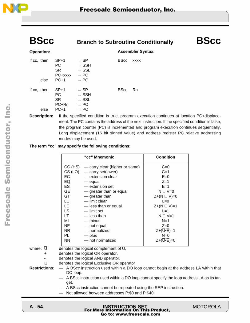
Fre
esc
ale
Se
mic
on
du
cto
r, I
Freescale Semiconductor, Inc.n
c..
.
Operation: Assembler Syntax:
If cc, then SP+1 → SP BScc xxxxPC → SSHSR → SSLPC+xxxx → PC
else PC+1 → PC
If cc, then SP+1 → SP BScc RnPC → SSHSR → SSLPC+Rn → PC
else PC+1 → PC
Description: If the specified condition is true, program execution continues at location PC+displace-ment. The PC contains the address of the next instruction. If the specified condition is false,the program counter (PC) is incremented and program execution continues sequentially.Long displacement (16 bit signed value) and address register PC relative addressingmodes may be used.
The term “cc” may specify the following conditions:
where: U denotes the logical complement of U,+ denotes the logical OR operator,• denotes the logical AND operator,⊕ denotes the logical Exclusive OR operator
Restrictions: — A BScc instruction used within a DO loop cannot begin at the address LA within thatDO loop.
— A BScc instruction used within a DO loop cannot specify the loop address LA as its tar-get.
— A BScc instruction cannot be repeated using the REP instruction.— Not allowed between addresses P:$0 and P:$40.
BScc Branch to Subroutine Conditionally BScc
“cc” Mnemonic Condition
CC (HS) — carry clear (higher or same) C=0CS (LO) — carry set(lower) C=1EC — extension clear E=0EQ — equal Z=1ES — extension set E=1GE — greater than or equal N ⊕ V=0GT — greater than Z+(N ⊕ V)=0LC — limit clear L=0LE — less than or equal Z+(N ⊕ V)=1LS — limit set L=1LT — less than N ⊕ V=1MI — minus N=1NE — not equal Z=0NR — normalized Z+(U•E)=1PL — plus N=0NN — not normalized Z+(U•E)=0
A - 54 INSTRUCTION SET MOTOROLA For More Information On This Product,
Go to: www.freescale.com
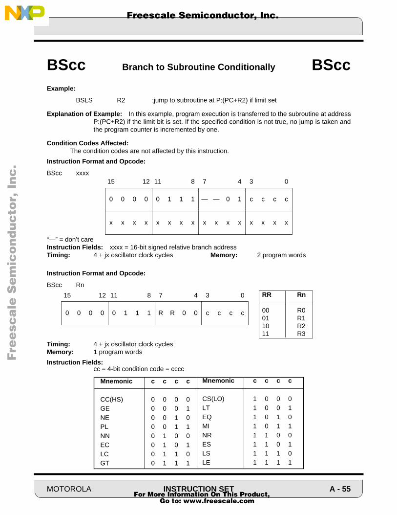
F
ree
sca
le S
em
ico
nd
uc
tor,
I
Freescale Semiconductor, Inc.n
c..
.
Example:
BSLS R2 ;jump to subroutine at P:(PC+R2) if limit set
Explanation of Example: In this example, program execution is transferred to the subroutine at addressP:(PC+R2) if the limit bit is set. If the specified condition is not true, no jump is taken andthe program counter is incremented by one.
Condition Codes Affected:The condition codes are not affected by this instruction.
Instruction Format and Opcode:
BScc xxxx
“—” = don’t careInstruction Fields: xxxx = 16-bit signed relative branch addressTiming: 4 + jx oscillator clock cycles Memory: 2 program words
Instruction Format and Opcode:
BScc Rn
Timing: 4 + jx oscillator clock cyclesMemory: 1 program words
Instruction Fields:cc = 4-bit condition code = cccc
BScc Branch to Subroutine Conditionally BScc
x x x x x x x x x x x x x x x x
0 0 0 0 0 1 1 1 — — 0 1 c c c c
15 12 11 8 7 4 3 0
0 0 0 0 0 1 1 1 R R 0 0 c c c c
15 12 11 8 7 4 3 0 RR Rn
00 R001 R110 R211 R3
Mnemonic c c c c
CC(HS) 0 0 0 0GE 0 0 0 1NE 0 0 1 0PL 0 0 1 1NN 0 1 0 0EC 0 1 0 1LC 0 1 1 0GT 0 1 1 1
Mnemonic c c c c
CS(LO) 1 0 0 0LT 1 0 0 1EQ 1 0 1 0MI 1 0 1 1NR 1 1 0 0ES 1 1 0 1LS 1 1 1 0LE 1 1 1 1
MOTOROLA INSTRUCTION SET A - 55 For More Information On This Product,
Go to: www.freescale.com

Fre
esc
ale
Se
mic
on
du
cto
r, I
Freescale Semiconductor, Inc.n
c..
.
Assembler Syntax: Operation:
SP+1 → SP BSR xxxxPC → SSHSR → SSLPC+xxxx → PC
SP+1 → SP BSR RnPC → SSHSR → SSLPC+Rn → PC
Description: Branch to subroutine in program memory at location PC+displacement. The PC containsthe address of the next instruction. Long displacement (16 bit signed value) and addressregister PC relative addressing modes may be used.
Restrictions: — A BSR instruction used within a DO loop cannot begin at the address LA within that DOloop.
— A BSR instruction used within a DO loop cannot specify the loop address LA as its tar-get.
— A BSR instruction cannot be repeated using the REP instruction.
— Not allowed between addresses P:$0 and P:$40.
Example:
BSR R2 ;jump to P:(PC+R2)
Explanation of Example:In this example, program execution is transferred the subroutine at address P:(PC+R2)
Condition Codes Affected:
The condition codes are not affected by this instruction.
BSR Branch to Subroutine BSR
A - 56 INSTRUCTION SET MOTOROLA For More Information On This Product,
Go to: www.freescale.com
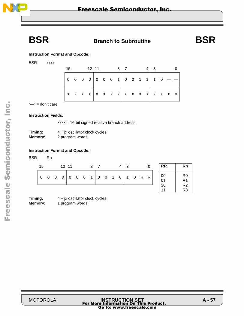
Fre
esc
ale
Se
mic
on
du
cto
r, I
Freescale Semiconductor, Inc.n
c..
.
Instruction Format and Opcode:
BSR xxxx
“—” = don’t care
Instruction Fields:
xxxx = 16-bit signed relative branch address
Timing: 4 + jx oscillator clock cyclesMemory: 2 program words
Instruction Format and Opcode:
BSR Rn
Timing: 4 + jx oscillator clock cyclesMemory: 1 program words
BSR Branch to Subroutine BSR
x x x x x x x x x x x x x x x x
0 0 0 0 0 0 0 1 0 0 1 1 1 0 — —
15 12 11 8 7 4 3 0
0 0 0 0 0 0 0 1 0 0 1 0 1 0 R R
15 12 11 8 7 4 3 0 RR Rn
00 R001 R110 R211 R3
MOTOROLA INSTRUCTION SET A - 57 For More Information On This Product,
Go to: www.freescale.com
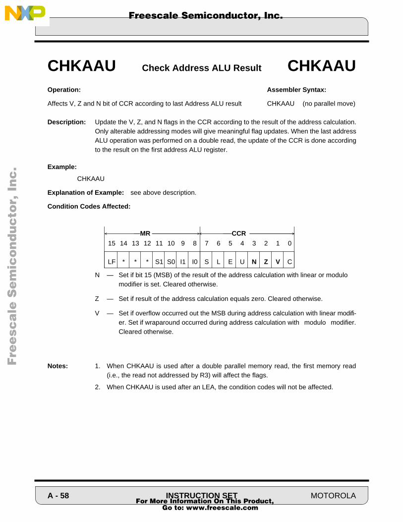
Fre
esc
ale
Se
mic
on
du
cto
r, I
Freescale Semiconductor, Inc.n
c..
.
Operation: Assembler Syntax:
Affects V, Z and N bit of CCR according to last Address ALU result CHKAAU (no parallel move)
Description: Update the V, Z, and N flags in the CCR according to the result of the address calculation.Only alterable addressing modes will give meaningful flag updates. When the last addressALU operation was performed on a double read, the update of the CCR is done accordingto the result on the first address ALU register.
Example:
CHKAAU
Explanation of Example: see above description.
Condition Codes Affected:
N — Set if bit 15 (MSB) of the result of the address calculation with linear or modulomodifier is set. Cleared otherwise.
Z — Set if result of the address calculation equals zero. Cleared otherwise.
V — Set if overflow occurred out the MSB during address calculation with linear modifi-er. Set if wraparound occurred during address calculation with modulo modifier.Cleared otherwise.
Notes: 1. When CHKAAU is used after a double parallel memory read, the first memory read(i.e., the read not addressed by R3) will affect the flags.
2. When CHKAAU is used after an LEA, the condition codes will not be affected.
CHKAAU Check Address ALU Result CHKAAU
15 14 13 12 11 10 9 8 7 6 5 4 3 2 1 0
LF * * * S1 S0 I1 I0 S L E U N Z V C
CCRMR
A - 58 INSTRUCTION SET MOTOROLA For More Information On This Product,
Go to: www.freescale.com
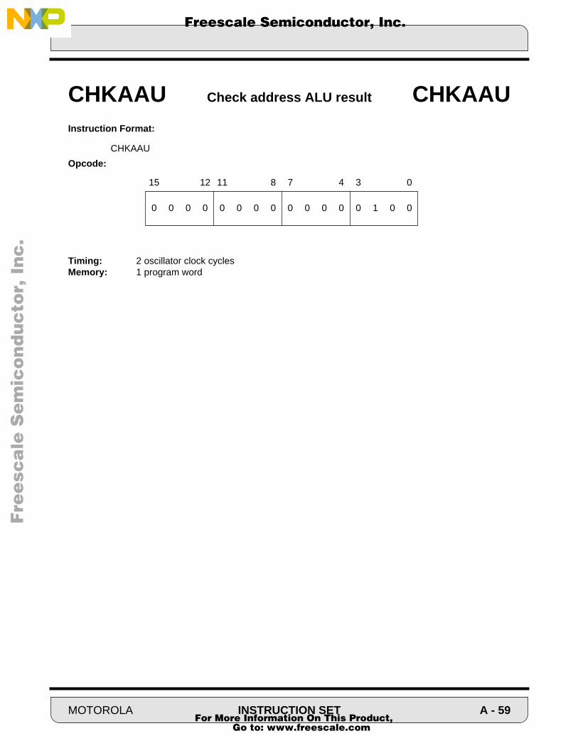
Fre
esc
ale
Se
mic
on
du
cto
r, I
Freescale Semiconductor, Inc.n
c..
.
Instruction Format:
CHKAAU
Opcode:
Timing: 2 oscillator clock cyclesMemory: 1 program word
CHKAAU Check address ALU result CHKAAU
0 0 0 0 0 0 0 0 0 0 0 0 0 1 0 0
15 12 11 8 7 4 3 0
MOTOROLA INSTRUCTION SET A - 59 For More Information On This Product,
Go to: www.freescale.com
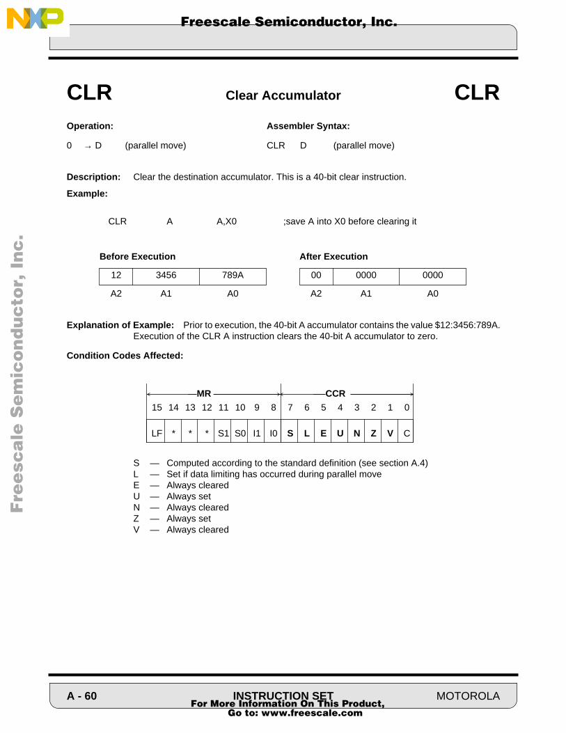
F
ree
sca
le S
em
ico
nd
uc
tor,
I
Freescale Semiconductor, Inc.n
c..
.
Operation: Assembler Syntax:
0 → D (parallel move) CLR D (parallel move)
Description: Clear the destination accumulator. This is a 40-bit clear instruction.
Example:
CLR A A,X0 ;save A into X0 before clearing it
Explanation of Example: Prior to execution, the 40-bit A accumulator contains the value $12:3456:789A.Execution of the CLR A instruction clears the 40-bit A accumulator to zero.
Condition Codes Affected:
S — Computed according to the standard definition (see section A.4)L — Set if data limiting has occurred during parallel moveE — Always clearedU — Always setN — Always clearedZ — Always setV — Always cleared
CLR Clear Accumulator CLR
After Execution
00 0000 0000
A2 A1 A0
Before Execution
12 3456 789A
A2 A1 A0
15 14 13 12 11 10 9 8 7 6 5 4 3 2 1 0
LF * * * S1 S0 I1 I0 S L E U N Z V C
CCRMR
A - 60 INSTRUCTION SET MOTOROLA For More Information On This Product,
Go to: www.freescale.com

F
ree
sca
le S
em
ico
nd
uc
tor,
I
Freescale Semiconductor, Inc.n
c..
.
Instruction Format:
CLR D (parallel move)Opcode:
Instruction Fields: Please see the “X Memory Data Move” description in the parallel move section for details on the m, RR, HHH, and W data fields.
Timing: 2 + mv oscillator clock cyclesMemory: 1 program word
CLR Clear Accumulator CLR
1 m R R H H H W 0 0 0 0 F 0 0 1
15 12 11 8 7 4 3 0
D F
A 0B 1
MOTOROLA INSTRUCTION SET A - 61 For More Information On This Product,
Go to: www.freescale.com
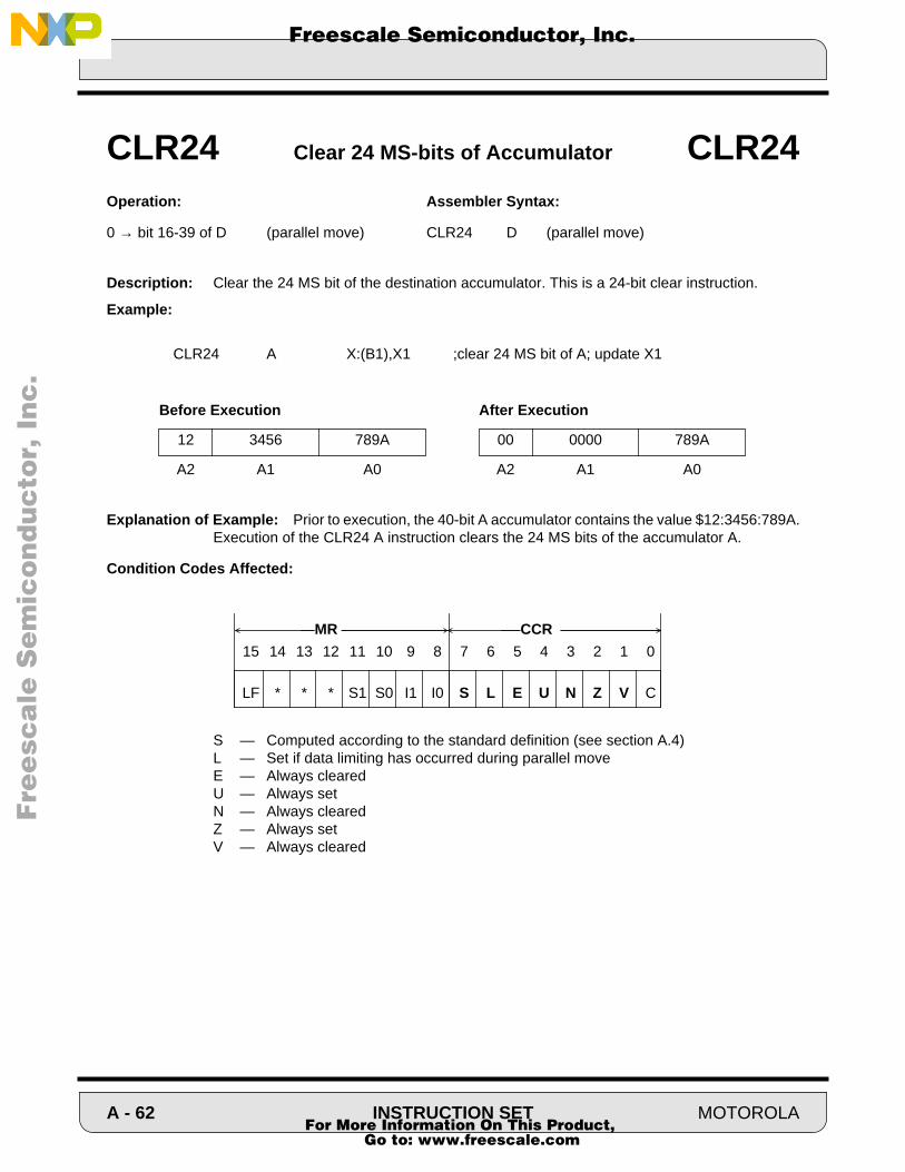
F
ree
sca
le S
em
ico
nd
uc
tor,
I
Freescale Semiconductor, Inc.n
c..
.
Operation: Assembler Syntax:
0 → bit 16-39 of D (parallel move) CLR24 D (parallel move)
Description: Clear the 24 MS bit of the destination accumulator. This is a 24-bit clear instruction.
Example:
CLR24 A X:(B1),X1 ;clear 24 MS bit of A; update X1
Explanation of Example: Prior to execution, the 40-bit A accumulator contains the value $12:3456:789A.Execution of the CLR24 A instruction clears the 24 MS bits of the accumulator A.
Condition Codes Affected:
S — Computed according to the standard definition (see section A.4)L — Set if data limiting has occurred during parallel moveE — Always clearedU — Always setN — Always clearedZ — Always setV — Always cleared
CLR24 Clear 24 MS-bits of Accumulator CLR24
After Execution
00 0000 789A
A2 A1 A0
Before Execution
12 3456 789A
A2 A1 A0
15 14 13 12 11 10 9 8 7 6 5 4 3 2 1 0
LF * * * S1 S0 I1 I0 S L E U N Z V C
CCRMR
A - 62 INSTRUCTION SET MOTOROLA For More Information On This Product,
Go to: www.freescale.com

F
ree
sca
le S
em
ico
nd
uc
tor,
I
Freescale Semiconductor, Inc.n
c..
.
Instruction Format:
CLR24 D (parallel move)Opcode:
Instruction Fields: Please see the “X Memory Data Move” description in the parallel move section for details on the m, RR, HHH, and W data fields.
Timing: 2 + mv oscillator clock cyclesMemory: 1 program word
CLR24 Clear 24 MS-bits of Accumulator CLR24
1 m R R H H H W 0 1 0 1 F 0 0 1
15 12 11 8 7 4 3 0
D F
A 0B 1
MOTOROLA INSTRUCTION SET A - 63 For More Information On This Product,
Go to: www.freescale.com

F
ree
sca
le S
em
ico
nd
uc
tor,
I
Freescale Semiconductor, Inc.n
c..
.
Operation: Assembler Syntax:
D - S (parallel move) CMP S,D (parallel move)
Description: Subtract the two operands and update the condition code register. The result of the sub-traction operation is not stored.
Note: This instruction subtracts 40-bit operands. When a word is specified as S, it is sign extended andzero filled to form a valid 40-bit operand. In order for the carry to be set correctly as a result of thesubtraction, D must be properly sign extended. D can be improperly sign extended by writing A1or B1 explicitly prior to executing the compare so that A2 or B2, respectively, may not represent thecorrect sign extension. This note particularly applies to the case where it is extended to compare16-bit operands such as X0 with A1.
Example:
CMP Y0,A X0,X:(R1)+N1 ;comp. Y0 and A, save X0
Explanation of Example: Prior to execution, the 40-bit A accumulator contains the value $00:0020:0000and the 16-bit Y0 register contains the value $0024. Execution of the CMP Y0,A instructionautomatically appends the 16-bit value in the Y0 register with 16 LS zeros, sign extends theresulting 32-bit long word to 40 bits, subtracts the result from the 40-bit A accumulator andupdates the condition code register leaving accumulator A unchanged.
CMP Compare CMP
After Execution
00 0020 0000
A2 A1 A0
Before Execution
00 0020 0000
A2 A1 A0
0024
Y0
0024
Y0
0319
SR=MR:CCR
0300
SR=MR:CCR
A - 64 INSTRUCTION SET MOTOROLA For More Information On This Product,
Go to: www.freescale.com

F
ree
sca
le S
em
ico
nd
uc
tor,
I
Freescale Semiconductor, Inc.n
c..
.
Condition Codes Affected:
S — Computed according to the standard definition (see section A.4)L — Set if limiting (parallel move) or overflow has occurred in resultE — Set if the signed integer portion of the result is in useU — Set if result is unnormalizedN — Set if bit 39 of the result is setZ — Set if result equals zeroV — Set if overflow has occurred in resultC — Set if a carry (or borrow) occurs from bit 39 of the result
Note: The definition of the E and U bits varies according to the scaling mode being used. Please refer toSection A.4 entitled “Condition Code Computation” for complete details.
Instruction Format:
CMP S,D (parallel move)Opcode:
Instruction Fields: Please see the “X Memory Data Move” description in the parallel move section for details on the m, RR, HHH, and W data fields.
Timing: 2 + mv oscillator clock cyclesMemory: 1 program word
CMP Compare CMP
15 14 13 12 11 10 9 8 7 6 5 4 3 2 1 0
LF * * * S1 S0 I1 I0 S L E U N Z V C
CCRMR
1 m R R H H H W 0 1 0 1 F J J J
15 12 11 8 7 4 3 0
S,D J J J FB,A 0 0 0 0A,B 0 0 0 1X0,A 1 0 0 0X0,B 1 0 0 1Y0,A 1 0 1 0
S,D J J J FY0,B 1 0 1 1X1,A 1 1 0 0X1,B 1 1 0 1Y1,A 1 1 1 0Y1,B 1 1 1 1
MOTOROLA INSTRUCTION SET A - 65 For More Information On This Product,
Go to: www.freescale.com

F
ree
sca
le S
em
ico
nd
uc
tor,
I
Freescale Semiconductor, Inc.n
c..
.
Operation: Assembler Syntax:
|D| - |S| (parallel move) CMPM S,D (parallel move)
Description: Subtract the two operands and update the condition code register. The result of the sub-traction operation is not stored.
Note: This instruction subtracts absolute values (magnitude) of 40-bit operands. When a word is specifiedas S, it is sign extended and zero filled to form a valid 40-bit operand. In order for the carry to beset correctly as a result of the subtraction, D must be properly sign extended. D can be improperlysign extended by writing A1 or B1 explicitly prior to executing the compare so that A2 or B2, respec-tively, may not represent the correct sign extension. This note particularly applies to the casewhere it is extended to compare 16-bit operands such as X0 with A1.
Example:
CMPM Y0,A X:(B1),X1 ;comp. |Y0| and |A|, update X1
Explanation of Example: Prior to execution, the 40-bit A accumulator contains the value $00:0006:0000and the 16-bit Y0 register contains the value $FFF7. Execution of the CMPM Y0,A instruc-tion automatically appends the 16-bit value in the Y0 register with 16 LS zeros, sign extendsthe resulting 32-bit long word to 40 bits, takes the absolute value of the resulting number,subtracts the result from the absolute value of the 40-bit A accumulator and updates thecondition code register leaving the accumulator A unchanged.
CMPM Compare Magnitude CMPM
After Execution
00 0006 0000
A2 A1 A0
Before Execution
00 0006 0000
A2 A1 A0
FFF7
Y0
FFF7
Y0
0019
SR=MR:CCR
0000
SR=MR:CCR
A - 66 INSTRUCTION SET MOTOROLA For More Information On This Product,
Go to: www.freescale.com

F
ree
sca
le S
em
ico
nd
uc
tor,
I
Freescale Semiconductor, Inc.n
c..
.
Condition Codes Affected:
S — Computed according to the standard definition (see section A.4)L — Set if limiting (parallel move) or overflow has occurred in resultE — Set if the signed integer portion of the result is in useU — Set if result is unnormalizedN — Set if bit 39 of the result is setZ — Set if result equals zeroV — Set if overflow has occurred in resultC — Set if a carry (or borrow) occurs from bit 39 of the result
Note: The definition of the E and U bits varies according to the scaling mode being used. Please refer toSection A.4 entitled “Condition Code Computation” for complete details.
Instruction Format:
CMPM S,D (parallel move)Opcode:
Instruction Fields: Please see the “X Memory Data Move” description in the parallel move section for details on the m, RR, HHH, and W data fields.
Timing: 2 + mv oscillator clock cyclesMemory: 1 program word
CMPM Compare Magnitude CMPM
15 14 13 12 11 10 9 8 7 6 5 4 3 2 1 0
LF * * * S1 S0 I1 I0 S L E U N Z V C
CCRMR
1 m R R H H H W 0 1 1 1 F J J J
15 12 11 8 7 4 3 0
S,D J J J FB,A 0 0 0 0A,B 0 0 0 1X0,A 1 0 0 0X0,B 1 0 0 1Y0,A 1 0 1 0
S,D J J J FY0,B 1 0 1 1X1,A 1 1 0 0X1,B 1 1 0 1Y1,A 1 1 1 0Y1,B 1 1 1 1
MOTOROLA INSTRUCTION SET A - 67 For More Information On This Product,
Go to: www.freescale.com

F
ree
sca
le S
em
ico
nd
uc
tor,
I
Freescale Semiconductor, Inc.n
c..
.
Operation: Assembler Syntax:
Enter the debug mode DEBUG
Description: Enter the debug mode and wait for OnCE commands.
Condition Codes Affected: Not affected
DEBUG Enter Debug Mode DEBUG
A - 68 INSTRUCTION SET MOTOROLA For More Information On This Product,
Go to: www.freescale.com

F
ree
sca
le S
em
ico
nd
uc
tor,
I
Freescale Semiconductor, Inc.n
c..
.
Instruction Format:
DEBUGOpcode:
Timing: 4 oscillator clock cyclesMemory: 1 program word
DEBUG Enter Debug Mode DEBUG
0 0 0 0 0 0 0 0 0 0 0 0 0 0 0 1
15 12 11 8 7 4 3 0
MOTOROLA INSTRUCTION SET A - 69 For More Information On This Product,
Go to: www.freescale.com

F
ree
sca
le S
em
ico
nd
uc
tor,
I
Freescale Semiconductor, Inc.n
c..
.
Operation: Assembler Syntax:
If cc, then enter the debug mode DEBUGccelse PC+1 → PC
Description: If the specified condition is true, enter the debug mode and wait for OnCE commands. Ifthe specified condition is false, continue with the next instruction.
The term “cc” may specify the following conditions:
where: U denotes the logical complement of U,+ denotes the logical OR operator,• denotes the logical AND operator,⊕ denotes the logical Exclusive OR operator
Example: The following is an example on conditional breakpoint setting using Debugcc:
DEBUGcc Enter Debug Mode Conditional DEBUGcc
“cc” Mnemonic Condition
CC (HS) — carry clear (higher or same) C=0CS (LO) — carry set(lower) C=1EC — extension clear E=0EQ — equal Z=1ES — extension set E=1GE — greater than or equal N ⊕ V=0GT — greater than Z+(N ⊕ V)=0LC — limit clear L=0LE — less than or equal Z+(N ⊕ V)=1LS — limit set L=1LT — less than N ⊕ V=1MI — minus N=1NE — not equal Z=0NR — normalized Z+(U•E)=1PL — plus N=0NN — not normalized Z+(U•E)=0
By replacing the MAC instruction by a JSR instruction as follows:
:ASR4 AJSR BreakADD X1,A::
Break DEBUGccMAC X0,Y1,ARTS
A conditional breakpoint can be set on the MAC instruction of the fol-lowing sequence of code::ASR4 AMAC X0,Y1,AADD X1,A
A - 70 INSTRUCTION SET MOTOROLA For More Information On This Product,
Go to: www.freescale.com

F
ree
sca
le S
em
ico
nd
uc
tor,
I
Freescale Semiconductor, Inc.n
c..
.
Condition Codes Affected: Not affected
Instruction Format:
DEBUGccOpcode:
Instruction Fields:
cc = 4-bit condition code = cccc
Timing: 4 oscillator clock cyclesMemory: 1 program word
DEBUGcc Enter Debug Mode Conditional DEBUGcc
0 0 0 0 0 0 0 0 0 1 0 1 c c c c
15 12 11 8 7 4 3 0
Mnemonic c c c c
CC(HS) 0 0 0 0GE 0 0 0 1NE 0 0 1 0PL 0 0 1 1NN 0 1 0 0EC 0 1 0 1LC 0 1 1 0GT 0 1 1 1
Mnemonic c c c c
CS(LO) 1 0 0 0LT 1 0 0 1EQ 1 0 1 0MI 1 0 1 1NR 1 1 0 0ES 1 1 0 1LS 1 1 1 0LE 1 1 1 1
MOTOROLA INSTRUCTION SET A - 71 For More Information On This Product,
Go to: www.freescale.com
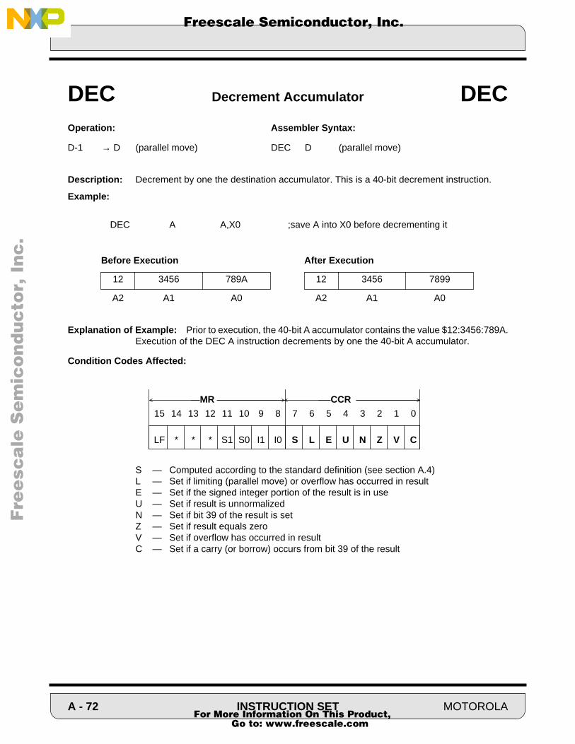
F
ree
sca
le S
em
ico
nd
uc
tor,
I
Freescale Semiconductor, Inc.n
c..
.
Operation: Assembler Syntax:
D-1 → D (parallel move) DEC D (parallel move)
Description: Decrement by one the destination accumulator. This is a 40-bit decrement instruction.
Example:
DEC A A,X0 ;save A into X0 before decrementing it
Explanation of Example: Prior to execution, the 40-bit A accumulator contains the value $12:3456:789A.Execution of the DEC A instruction decrements by one the 40-bit A accumulator.
Condition Codes Affected:
S — Computed according to the standard definition (see section A.4)L — Set if limiting (parallel move) or overflow has occurred in resultE — Set if the signed integer portion of the result is in useU — Set if result is unnormalizedN — Set if bit 39 of the result is setZ — Set if result equals zeroV — Set if overflow has occurred in resultC — Set if a carry (or borrow) occurs from bit 39 of the result
DEC Decrement Accumulator DEC
After Execution
12 3456 7899
A2 A1 A0
Before Execution
12 3456 789A
A2 A1 A0
15 14 13 12 11 10 9 8 7 6 5 4 3 2 1 0
LF * * * S1 S0 I1 I0 S L E U N Z V C
CCRMR
A - 72 INSTRUCTION SET MOTOROLA For More Information On This Product,
Go to: www.freescale.com
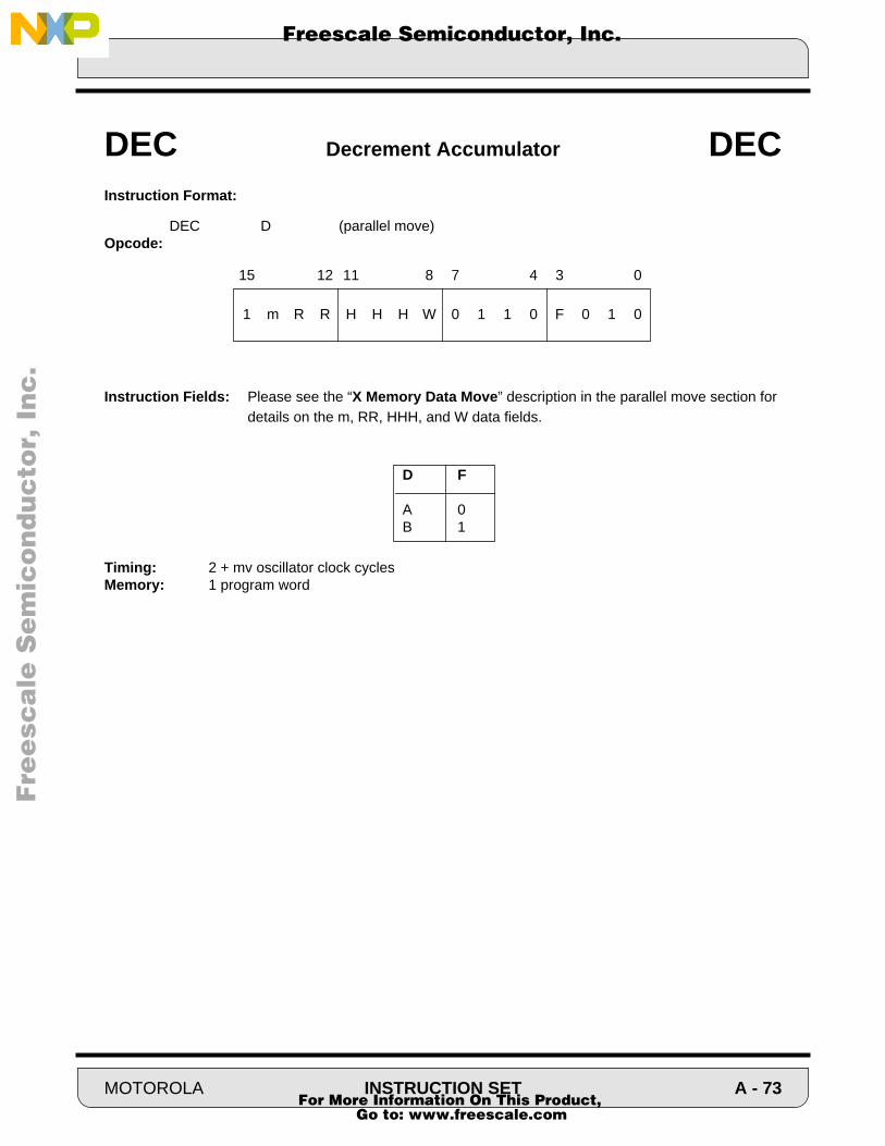
F
ree
sca
le S
em
ico
nd
uc
tor,
I
Freescale Semiconductor, Inc.n
c..
.
Instruction Format:
DEC D (parallel move)Opcode:
Instruction Fields: Please see the “X Memory Data Move” description in the parallel move section for details on the m, RR, HHH, and W data fields.
Timing: 2 + mv oscillator clock cyclesMemory: 1 program word
DEC Decrement Accumulator DEC
1 m R R H H H W 0 1 1 0 F 0 1 0
15 12 11 8 7 4 3 0
D F
A 0B 1
MOTOROLA INSTRUCTION SET A - 73 For More Information On This Product,
Go to: www.freescale.com

F
ree
sca
le S
em
ico
nd
uc
tor,
I
Freescale Semiconductor, Inc.n
c..
.
Operation: Assembler Syntax:
D2:D1-1 → D2:D1 (parallel move); DEC24 D (parallel move)D0 is unchanged
Description: Decrement by one the 24 MS bits of the destination accumulator.
Example:
DEC24 A X:(B1),X1 ;Decrement 24 MS bit of A; update X1
Explanation of Example: Prior to execution, the 40-bit A accumulator contains the value $12:3456:789A.Execution of the DEC24 A instruction decrements by one the 24 MS bit of the accumulatorA.
Condition Codes Affected:
S — Computed according to the standard definition (see section A.4)L — Set if limiting (parallel move) or overflow has occurred in resultE — Set if the signed integer portion of the result is in useU — Set if result is unnormalizedN — Set if bit 39 of the result is setZ — Set if the 24 most significant bit of the result are all zeroesV — Set if overflow has occurred in resultC — Set if a carry (or borrow) occurs from bit 39 of the result
DEC24 Decrement 24 MS-bit of Accumulator DEC24
After Execution
12 3455 789A
A2 A1 A0
Before Execution
12 3456 789A
A2 A1 A0
15 14 13 12 11 10 9 8 7 6 5 4 3 2 1 0
LF * * * S1 S0 I1 I0 S L E U N Z V C
CCRMR
A - 74 INSTRUCTION SET MOTOROLA For More Information On This Product,
Go to: www.freescale.com
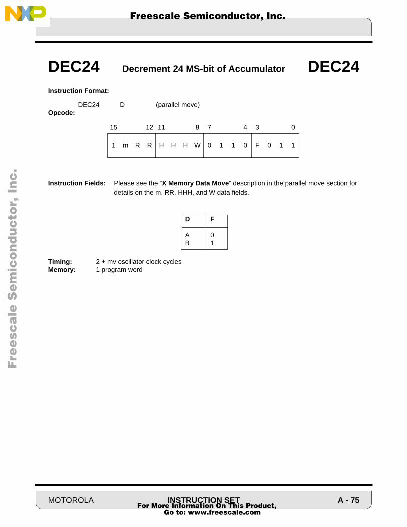
F
ree
sca
le S
em
ico
nd
uc
tor,
I
Freescale Semiconductor, Inc.n
c..
.
Instruction Format:
DEC24 D (parallel move)Opcode:
Instruction Fields: Please see the “X Memory Data Move” description in the parallel move section for details on the m, RR, HHH, and W data fields.
Timing: 2 + mv oscillator clock cyclesMemory: 1 program word
DEC24 Decrement 24 MS-bit of Accumulator DEC24
1 m R R H H H W 0 1 1 0 F 0 1 1
15 12 11 8 7 4 3 0
D F
A 0B 1
MOTOROLA INSTRUCTION SET A - 75 For More Information On This Product,
Go to: www.freescale.com

F
ree
sca
le S
em
ico
nd
uc
tor,
I
Freescale Semiconductor, Inc.n
c..
.
Assembler Syntax:
DIV S,D (parallel move)
Operation:
Description: Divide the destination operand D (dividend) by the source operand S (divisor) and store theresult in the destination accumulator D. The 32-bit dividend must be a positive fractionwhich has been sign extended to 40-bits and is stored in the full 40-bit destinationaccumulator D. The 16-bit divisor is a signed fraction and is stored in the source op-erand S. Each DIV iteration calculates one quotient bit using a nonrestoring fractional divi-sion algorithm (see the description on the next page). After execution of the first DIV in-struction, the destination operand holds both the partial remainder and the formed quotient.The partial remainder occupies the high order portion of the destination accumulator D andis a signed fraction. The formed quotient occupies the low order portion of the destinationaccumulator D (A0 or B0) and is a positive fraction. One bit of the formed quotient is shiftedinto the LSB of the destination accumulator at the start of each DIV iteration. The formedquotient is the true quotient if the true quotient is positive. If the true quotient is negative,the formed quotient must be negated. Valid results are obtained only when |D| < |S| andthe operands are interpreted as fractions. Note that this condition ensures that the mag-nitude of the quotient is less than one (i.e., is fractional) and precludes division by zero.The DIV instruction calculates one quotient bit based on the divisor and the previous partialremainder. To produce an N-bit quotient, the DIV instruction is executed N times where Nis the number of bits of precision desired in the quotient, 1< N<16. Thus, for a full precision(16 bit) quotient, 16 DIV iterations are required. In general, executing the DIV instruction Ntimes produces an N-bit quotient and a 32-bit remainder which has (32 - N) bits of precisionand whose N MS bits are zeros. The partial remainder is not a true remainder and must becorrected due to the nonrestoring nature of the division algorithm before it may be used.Therefore, once the divide is complete, it is necessary to reverse the last DIV operation andrestore the remainder to obtain the true remainder.
The DIV instruction uses a nonrestoring fractional division algorithm which consists of the following opera-tions:
1. Compare the source and destination operand sign bits: An exclusive OR operation is performed on bit 39 of the destination operand D and bit 15 of the source operand S;
DIV Divide Iteration DIV
If D[39] ⊕ S[15] = 1 then
C; D1+ S → D1
D2 D1 D0
else
C; D1 - S → D1
D2 D1 D0
A - 76 INSTRUCTION SET MOTOROLA For More Information On This Product,
Go to: www.freescale.com
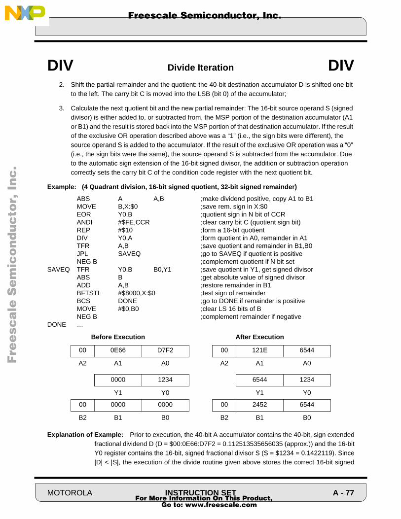
F
ree
sca
le S
em
ico
nd
uc
tor,
I
Freescale Semiconductor, Inc.n
c..
.
2. Shift the partial remainder and the quotient: the 40-bit destination accumulator D is shifted one bit to the left. The carry bit C is moved into the LSB (bit 0) of the accumulator;
3. Calculate the next quotient bit and the new partial remainder: The 16-bit source operand S (signed divisor) is either added to, or subtracted from, the MSP portion of the destination accumulator (A1 or B1) and the result is stored back into the MSP portion of that destination accumulator. If the result of the exclusive OR operation described above was a “1” (i.e., the sign bits were different), the source operand S is added to the accumulator. If the result of the exclusive OR operation was a “0” (i.e., the sign bits were the same), the source operand S is subtracted from the accumulator. Due to the automatic sign extension of the 16-bit signed divisor, the addition or subtraction operation correctly sets the carry bit C of the condition code register with the next quotient bit.
Example: (4 Quadrant division, 16-bit signed quotient, 32-bit signed remainder)
ABS A A,B ;make dividend positive, copy A1 to B1MOVE B,X:$0 ;save rem. sign in X:$0 EOR Y0,B ;quotient sign in N bit of CCRANDI #$FE,CCR ;clear carry bit C (quotient sign bit)REP #$10 ;form a 16-bit quotientDIV Y0,A ;form quotient in A0, remainder in A1TFR A,B ;save quotient and remainder in B1,B0JPL SAVEQ ;go to SAVEQ if quotient is positiveNEG B ;complement quotient if N bit set
SAVEQ TFR Y0,B B0,Y1 ;save quotient in Y1, get signed divisorABS B ;get absolute value of signed divisorADD A,B ;restore remainder in B1BFTSTL #$8000,X:$0 ;test sign of remainderBCS DONE ;go to DONE if remainder is positiveMOVE #$0,B0 ;clear LS 16 bits of BNEG B ;complement remainder if negative
DONE …
Explanation of Example: Prior to execution, the 40-bit A accumulator contains the 40-bit, sign extendedfractional dividend D (D = $00:0E66:D7F2 = 0.112513535656035 (approx.)) and the 16-bitY0 register contains the 16-bit, signed fractional divisor S (S = $1234 = 0.1422119). Since|D| < |S|, the execution of the divide routine given above stores the correct 16-bit signed
DIV Divide Iteration DIV
After Execution
00 121E 6544
A2 A1 A0
Before Execution
00 0E66 D7F2
A2 A1 A0
00 2452 6544
B2 B1 B0
00 0000 0000
B2 B1 B0
6544 1234
Y1 Y0
0000 1234
Y1 Y0
MOTOROLA INSTRUCTION SET A - 77 For More Information On This Product,
Go to: www.freescale.com

F
ree
sca
le S
em
ico
nd
uc
tor,
I
Freescale Semiconductor, Inc.n
c..
.
quotient in the 16-bit Y1 register (A/Y0 = 0.7911072 = $6544 = Y1). The partial remainderis restored by reversing the last DIV operation and adding back the absolute value of thesigned divisor in Y0 to the partial remainder in A1. This produces the correct LS16 bits ofthe 32-bit signed remainder in the 16-bit B1 register. Note that the remainder is really a 32-bit value which has 16 bits of precision. Thus, the correct 32-bit remainder is $0000:2452which is approximately 0.000004329718649.
Note: The divide routine used in the example above assumes that the sign extended 40-bit signed frac-tional dividend is stored in the A accumulator and that the 16-bit signed fractional divisor is stored in the Y0 register. This routine produces a full 16-bit signed quotient and a 32-bit signed remainder. This routine may be greatly simplified for the case in which only unsigned operands are used to pro-duce a 16-bit positive quotient and a 32-bit positive remainder, as shown below.
1 Quadrant division, 16-bit unsigned quotient, 32-bit unsigned remainder
ANDI #$FE,CCR ;clear carry bit C (quotient sign bit)REP #$10 ;form a 16-bit quotient and remainderDIV X0,A ;form quotient in A0, remainder in A1ADD X0,A ;restore remainder in A1
This last routine assumes that the 40-bit positive, fractional, sign extended dividend is stored in the A accumulator and that the 16-bit positive, fractional divisor is stored in the X0 register. After exe-cution, the 16-bit positive fractional quotient is stored in the A0 register while the LS 16-bits of the 32-bit positive fractional remainder are stored in the A1 register.
DIV Divide Iteration DIV
A - 78 INSTRUCTION SET MOTOROLA For More Information On This Product,
Go to: www.freescale.com

F
ree
sca
le S
em
ico
nd
uc
tor,
I
Freescale Semiconductor, Inc.n
c..
.
Condition Codes Affected:
L — Set if overflow bit V is setV — Set if the MS bit of the destination operand is changed as a result of the
instruction’s left shift operationC — Set if bit 39 of the result is cleared
Instruction Format:
DIV S,D (parallel move)Opcode:
“—” = don’t care
Instruction Fields:
Timing: 2 oscillator clock cyclesMemory: 1 program word
DIV Divide Iteration DIV
15 14 13 12 11 10 9 8 7 6 5 4 3 2 1 0
LF * * * S1 S0 I1 I0 S L E U N Z V C
CCRMR
0 0 0 1 0 1 0 1 0 — — 0 F 1 D D
15 12 11 8 7 4 3 0
S,D D D F
X0,A 0 0 0X0,B 0 0 1Y0,A 0 1 0Y0,B 0 1 1
S,D D D F
X1,A 1 0 0X1,B 1 0 1Y1,A 1 1 0Y1,B 1 1 1
MOTOROLA INSTRUCTION SET A - 79 For More Information On This Product,
Go to: www.freescale.com
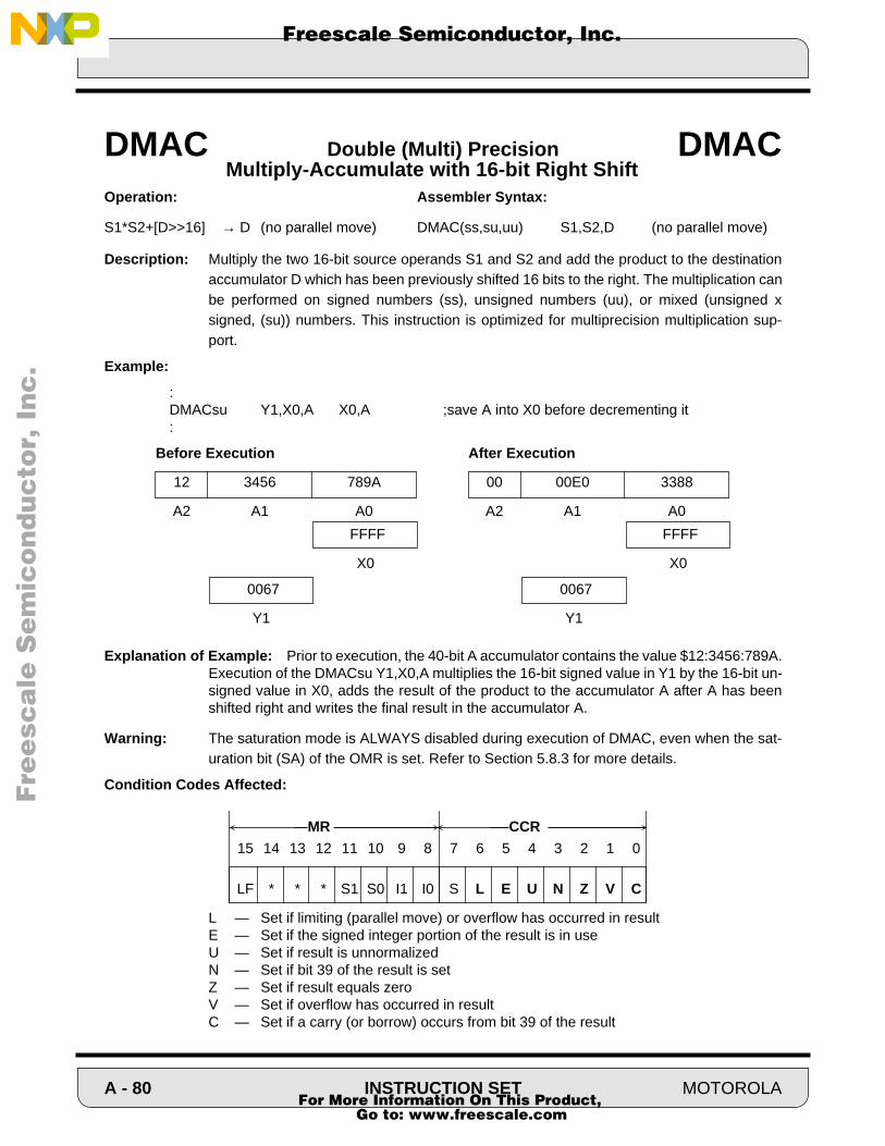
F
ree
sca
le S
em
ico
nd
uc
tor,
I
Freescale Semiconductor, Inc.n
c..
.
Operation: Assembler Syntax:
S1*S2+[D>>16] → D (no parallel move) DMAC(ss,su,uu) S1,S2,D (no parallel move)
Description: Multiply the two 16-bit source operands S1 and S2 and add the product to the destinationaccumulator D which has been previously shifted 16 bits to the right. The multiplication canbe performed on signed numbers (ss), unsigned numbers (uu), or mixed (unsigned xsigned, (su)) numbers. This instruction is optimized for multiprecision multiplication sup-port.
Example:
:DMACsu Y1,X0,A X0,A ;save A into X0 before decrementing it:
Explanation of Example: Prior to execution, the 40-bit A accumulator contains the value $12:3456:789A.Execution of the DMACsu Y1,X0,A multiplies the 16-bit signed value in Y1 by the 16-bit un-signed value in X0, adds the result of the product to the accumulator A after A has beenshifted right and writes the final result in the accumulator A.
Warning: The saturation mode is ALWAYS disabled during execution of DMAC, even when the sat-uration bit (SA) of the OMR is set. Refer to Section 5.8.3 for more details.
Condition Codes Affected:
L — Set if limiting (parallel move) or overflow has occurred in resultE — Set if the signed integer portion of the result is in useU — Set if result is unnormalizedN — Set if bit 39 of the result is setZ — Set if result equals zeroV — Set if overflow has occurred in resultC — Set if a carry (or borrow) occurs from bit 39 of the result
DMAC Double (Multi) Precision DMACMultiply-Accumulate with 16-bit Right Shift
FFFF
X0
After Execution
00 00E0 3388
A2 A1 A0
Before Execution
12 3456 789A
A2 A1 A0
0067
Y1
FFFF
X0
0067
Y1
15 14 13 12 11 10 9 8 7 6 5 4 3 2 1 0
LF * * * S1 S0 I1 I0 S L E U N Z V C
CCRMR
A - 80 INSTRUCTION SET MOTOROLA For More Information On This Product,
Go to: www.freescale.com
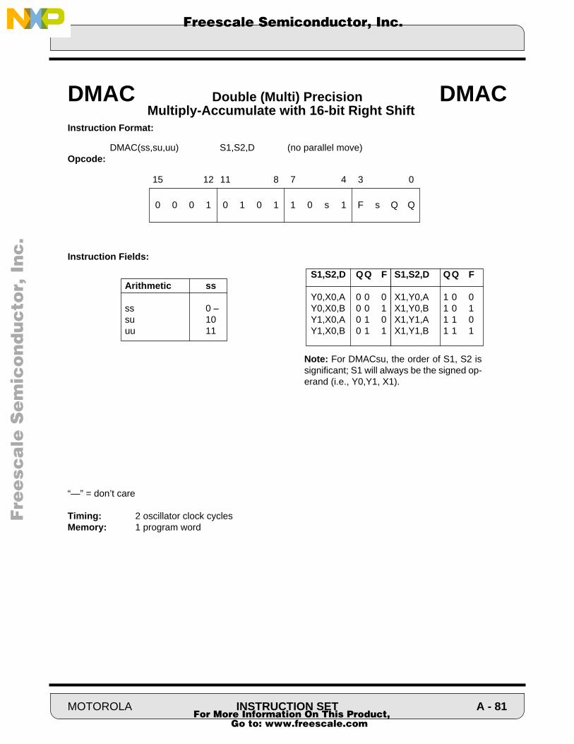
F
ree
sca
le S
em
ico
nd
uc
tor,
I
Freescale Semiconductor, Inc.n
c..
.
Instruction Format:
DMAC(ss,su,uu) S1,S2,D (no parallel move)Opcode:
Instruction Fields:
“—” = don’t care
Timing: 2 oscillator clock cyclesMemory: 1 program word
DMAC Double (Multi) Precision DMACMultiply-Accumulate with 16-bit Right Shift
0 0 0 1 0 1 0 1 1 0 s 1 F s Q Q
15 12 11 8 7 4 3 0
S1,S2,D QQ F
Y0,X0,A 0 0 0Y0,X0,B 0 0 1Y1,X0,A 0 1 0Y1,X0,B 0 1 1
S1,S2,D QQ F
X1,Y0,A 1 0 0X1,Y0,B 1 0 1X1,Y1,A 1 1 0X1,Y1,B 1 1 1
Arithmetic ss
ss 0 –su 10uu 11
Note: For DMACsu, the order of S1, S2 issignificant; S1 will always be the signed op-erand (i.e., Y0,Y1, X1).
MOTOROLA INSTRUCTION SET A - 81 For More Information On This Product,
Go to: www.freescale.com

F
ree
sca
le S
em
ico
nd
uc
tor,
I
Freescale Semiconductor, Inc.n
c..
.
Operation: Assembler Syntax:SP+1→SP; LA →SSH; LC→SSL; X:<ea> →LC DO X:(Rn),exprSP+1→SP; PC→SSH; SR→SSL; offset-1+PC→LA1→ LF
SP+1 → SP; LA → SSH; LC→ SSL; #xx → LC DO #xx,exprSP+1→SP; PC→SSH; SR→SSL; offset-1+PC→LA1→ LF
SP+1 → SP; LA → SSH; LC→ SSL; S → LC DO S,exprSP+1→SP; PC→SSH; SR→SSL; offset-1+PC→LA1→ LF
End of Loop:SSL(LF) → SR; SP-1 → SPSSH → LA; SSL → LC; SP-1 → SP
Description: Begin a hardware DO loop that is to be repeated the number of times specified in the in-struction’s source operand and whose range of execution is terminated by the destinationoperand (shown above as “expr”). No overhead other than the execution of this DO instruc-tion is required to set up this loop. DO loops can be nested and the loop count can bepassed as a parameter. During the first instruction cycle, the current contents of the LoopAddress (LA) and the Loop Counter (LC) registers are pushed onto the system stack. TheDO instruction’s source operand is then loaded into the Loop Counter (LC) register. The LCregister contains the remaining number of times the DO loop will be executed and can beaccessed from inside the DO loop subject to certain restrictions. If LC equals zero, the DOloop is not executed. If immediate short data is specified, the 8 LS bits of LC are loadedwith the 8-bit immediate value and the eight MS bits of LC are cleared.
During the second instruction cycle, the current contents of the Program Counter (PC) reg-ister and the Status Register (SR) are pushed onto the system stack. Stacking LA, LC, PC,and SR permits nesting DO loops. The DO instruction’s destination address (shown as off-set which is derived from “expr”) is then loaded into the Loop Address (LA) register afterhaving been added to the PC. This 16-bit operand is located in the instruction’s 16-bit rel-ative address extension word as shown in the opcode section. The value in the ProgramCounter (PC) register pushed onto the system stack is the address of the first instructionfollowing the DO instruction (i.e., the first actual instruction in the DO loop). This value isread (i.e., copied but not pulled) from the top of the system stack to return to the top of theloop for another pass through the loop.
During the third instruction cycle, the Loop Flag (LF) is set. This results in the PC being re-peatedly compared with LA to determine if the last instruction in the loop has been fetched.If LA equals PC, the last instruction in the loop has been fetched and the Loop Counter (LC)is tested. If LC is not equal to one, it is decremented by one and SSH is loaded into the PCto fetch the first instruction in the loop again. If LC equals one, the “end of loop” processingbegins.
DO Start Hardware Do Loop DO
A - 82 INSTRUCTION SET MOTOROLA For More Information On This Product,
Go to: www.freescale.com

F
ree
sca
le S
em
ico
nd
uc
tor,
I
Freescale Semiconductor, Inc.n
c..
.
When executing a DO loop, the instructions are actually fetched each time through the loop.Therefore, a DO loop can be interrupted. DO loops can also be nested. When DO loops arenested, the end of loop addresses must also be nested and are not allowed to be equal.The assembler generates an error message when DO loops are improperly nested. NestedDO loops are illustrated in the example.
Note: The assembler determines the offset needed to calculate the address to be loaded into LA at exe-cution time. This offset is calculated by evaluating the end of loop expression “expr” and subtractingthe address of the next instruction following the DO instruction. This is done to accommodate thecase where the last word in the DO loop is a two word instruction. Thus, the end of loop expression“expr” in the source code must represent the address of the instruction AFTER the last instructionin the loop as shown in the example.
During the “end of loop” processing, the Loop Flag (LF) from the lower portion (SSL) of SPis written into the Status Register (SR), the contents of the Loop Address (LA) register arerestored from the upper portion (SSH) of SP-1, the contents of the Loop Counter (LC) arerestored from the lower portion (SSL) of SP-1 and the Stack Pointer (SP) is decrementedby two. Instruction fetches now continue at the address of the instruction following the lastinstruction in the DO loop. Note that LF is the only bit in the Status Register (SR) that isrestored after a hardware DO loop has been exited.
Note: The Loop Flag (LF) is cleared by a hardware reset.
Restrictions: The “end of loop” comparison described above actually occurs at instruction fetch time. Thatis, LA is being compared with PC when the instruction at LA-2 is being executed. Therefore, instructionswhich access the program controller registers and/or change program flow cannot be used in locations LA-2, LA-1, or LA.
Proper DO loop operation is not guaranteed if an instruction starting at address LA-2, LA-1, or LA specifiesone of the program controller registers SR, SP, SSL, LA, LC, or (implicitly) PC as a destination register. Sim-ilarly, the SSH program controller register may not be specified as a source or destination register in an in-struction starting at address LA-2, LA-1, or LA. Additionally, the SSH register cannot be specified as asource register in the DO instruction itself and LA cannot be used as a target for jumps to subroutine (i.e.,BSR, JSR, BScc, or JScc to LA). A DO instruction cannot be repeated using the REP instruction.
DO Start Hardware Do Loop DO
MOTOROLA INSTRUCTION SET A - 83 For More Information On This Product,
Go to: www.freescale.com

F
ree
sca
le S
em
ico
nd
uc
tor,
I
Freescale Semiconductor, Inc.n
c..
.
The following instructions cannot begin at the indicated position(s) near the end of a DO loop:
At LA-2, LA-1 and LA DOMOVEC from SSHMOVEC to LA, LC, SR, SP, SSH or SSLANDI MRORI MRTwo word instructions which read LC, SP, or SSL
At LA-1 ENDDO, BRKccSingle word instructions which read LC, SP, or SSL
At LA any two-word instruction* RESETBcc, Jcc RTIBRA, JMP RTSBScc, JScc STOP
BSR, JSR WAITREP, REPcc
*This restriction applies to the situation in which the DSP Simulator’s single line assembler is used to changethe last instruction in a DO loop from a one-word instruction to a two-word instruction.
Other Restrictions DO SSH,xxxxBSR, JSR to (LA) whenever the Loop Flag (LF) is setBScc, JScc to (LA) whenever the Loop Flag (LF) is set
A DO instruction cannot be repeated using the REP instruction.
Notes: Due to pipelining, if an address register (R0-R3, N0-N3 or M0-M3) is changed using a move-typeinstruction (LUA, Tcc, MOVE, MOVEC, MOVEP, or parallel move), the new contents of the desti-nation address register will not be available for use during the following instruction (i.e., there is asingle instruction cycle pipeline delay). This restriction also applies to the situation in which the lastinstruction in a DO loop changes an address register and the first instruction at the top of the DOloop uses that same address register. The top instruction becomes the following instruction be-cause of the loop construct.
DO Start Hardware Do Loop DO
A - 84 INSTRUCTION SET MOTOROLA For More Information On This Product,
Go to: www.freescale.com

F
ree
sca
le S
em
ico
nd
uc
tor,
I
Freescale Semiconductor, Inc.n
c..
.
Similarly, since the DO instruction accesses the program controller registers, the DO instruction must notbe immediately preceded by any of the following instructions:
Immediately before DO MOVEC to LA, LC, SSH, SSL or SPMOVEC from SSH
Example:
DO #cnt1, END1 ;begin outer DO loop:
DO #cnt2, END2 ;begin inner DO loop::
MOVE A,X:(R0)+ ;last instruction in inner loopEND2 : ;(in outer loop)
ADD A,B X:(R1)+,X0 ;last instruction in outer loopEND1 : ;first instruction after outer loop
Explanation of Example: This example illustrates a nested DO loop. The outer DO loop will be executed“cnt1” times while the inner DO loop will be executed (“cnt1” * “cnt2”) times. Note that thelabels END1 and END2 are located at the first instruction past the end of the DO loop, asmentioned above, and are nested properly.
Condition Codes:
LF — Set when a DO loop is in progressL — Set if data limiting occurred
Note: If A or B is specified as a source operand, the accumulator value is optionally shifted according tothe scaling mode bits in the status register. If the data out of the shifter indicates that the accumu-lator extension is in use, the 16-bit data is limited to a maximum positive or negative saturation con-stant. The shifted and limited value is loaded into LC, although A or B remain unchanged.
DO Start Hardware Do Loop DO
15 14 13 12 11 10 9 8 7 6 5 4 3 2 1 0
LF * * * S1 S0 I1 I0 S L E U N Z V C
CCRMR
MOTOROLA INSTRUCTION SET A - 85 For More Information On This Product,
Go to: www.freescale.com

F
ree
sca
le S
em
ico
nd
uc
tor,
I
Freescale Semiconductor, Inc.n
c..
.
Instruction Format and Opcode:
DO X:(Rn), expr
“—” = don’t care
DO #xx, expr
DO Start Hardware Do Loop DO
Relative Address Displacement Extension
0 0 0 0 0 0 0 0 1 1 0 — — — R R
15 12 11 8 7 4 3 0
RR Rn
00 R001 R110 R211 R3
Relative Address Displacement Extension
0 0 0 0 1 1 1 0 i i i i i i i i
15 12 11 8 7 4 3 0
iiii = immediate 8-bit short data = iiiiiiii
A - 86 INSTRUCTION SET MOTOROLA For More Information On This Product,
Go to: www.freescale.com

F
ree
sca
le S
em
ico
nd
uc
tor,
I
Freescale Semiconductor, Inc.n
c..
.
DO S,expr
Note: • For DO SP, exprThe actual value that will be loaded into the Loop Counter (LC) is the value of the Stack Pointer(SP) before the execution of the DO instruction, incremented by one. Thus, if SP = 3, the execu-tion of the DO SP, expr instruction will load the Loop Counter (LC) with the value LC = 4.
• For DO SSL, exprThe Loop Counter (LC) will be loaded with its previous value which was saved on the stack bythe DO instruction itself.
• If A or B is specified as a source operand, the accumulator value is optionally shifted accordingto the scaling mode bits in the status register. If the data out of the shifter indicates that the accu-mulator extension is in use, the 16-bit data is limited to a maximum positive or negative saturationconstant. The shifted and limited value is loaded into LC, although A or B remain unchanged.
Instruction Field for the second word:
expr = 16-bit PC Relative Address
Timing: 10 + mv oscillator clock cycles if the DO argument equals zero; otherwise it is 6 + mv oscillator clock cycles
Memory: 2 program words
DO Start Hardware Do Loop DO
Relative Address Displacement Extension
0 0 0 0 0 1 0 0 0 0 0 D D D D D
15 12 11 8 7 4 3 0
S D D D D D
X0 0 0 0 0 0Y0 0 0 0 0 1X1 0 0 0 1 0Y1 0 0 0 1 1A 0 0 1 0 0B 0 0 1 0 1A0 0 0 1 1 0B0 0 0 1 1 1
S D D D D D
SR 0 1 0 0 1OMR 0 1 0 1 0SP 0 1 0 1 1A1 0 1 1 0 0B1 0 1 1 0 1A2 0 1 1 1 0B2 0 1 1 1 1
S D D D D D
R0 1 0 0 0 0R1 1 0 0 0 1R2 1 0 0 1 0R3 1 0 0 1 1M0 1 0 1 0 0M1 1 0 1 0 1M2 1 0 1 1 0M3 1 0 1 1 1
S D D D D D
SSH 1 1 0 0 0SSL 1 1 0 0 1LA 1 1 0 1 0LC 0 1 0 0 0N0 1 1 1 0 0N1 1 1 1 0 1N2 1 1 1 1 0N3 1 1 1 1 1
MOTOROLA INSTRUCTION SET A - 87 For More Information On This Product,
Go to: www.freescale.com
F
ree
sca
le S
em
ico
nd
uc
tor,
I
Freescale Semiconductor, Inc.n
c..
.
Operation: Assembler Syntax:
SP+1→SP; LA →SSH; LC→SSL DO FOREVER exprSP+1→SP; PC→SSH; SR→SSL; expr-1+PC→LA1→ LF; 1→FV
Description: Begin a hardware DO loop that is to be repeated for ever and whose range of execution isterminated by the destination operand (shown above as “expr”). No overhead other thanthe execution of this DO FOREVER instruction is required to set up this loop. DO FOREV-ER loops can be nested. During the first instruction cycle, the current contents of the LoopAddress (LA) and the Loop Counter (LC) registers are pushed onto the system stack. Theloop counter (LC) register is pushed onto the stack but is not updated by this instruction.
During the second instruction cycle, the current contents of the Program Counter (PC) reg-ister and the Status Register (SR) are pushed onto the system stack. Stacking the LA, LC,PC, and SR registers permits nesting DO FOREVER loops. The DO FOREVER instruc-tion’s destination operand (shown as “expr”) is then loaded into the Loop Address (LA) reg-ister after having been added to the PC. This 16-bit operand is located in the instruction’s16-bit relative address extension word as shown in the opcode section. The value in theProgram Counter (PC) register pushed onto the system stack is the address of the first in-struction following the DO FOREVER instruction (i.e., the first actual instruction in the DOFOREVER loop). This value is read (i.e., copied but not pulled) from the top of the systemstack to return to the top of the loop for another pass through the loop.
During the third instruction cycle, the Loop Flag (LF) and the ForeVer flag are set. This re-sults in the PC being repeatedly compared with LA to determine if the last instruction in theloop has been fetched. If LA equals PC, the last instruction in the loop has been fetchedand SSH is loaded into the PC to fetch the first instruction in the loop again. The loopcounter (LC) register is then decremented by one without being tested. This register can beused by the programer to count the number of loops already executed.
When executing a DO FOREVER loop, the instructions are actually fetched each timethrough the loop. Therefore, a DO FOREVER loop can be interrupted. DO FOREVER loopscan also be nested. When DO FOREVER loops are nested, the end of loop addresses mustalso be nested and are not allowed to be equal. The assembler generates an error mes-sage when DO FOREVER loops are improperly nested. Nested DO loops with one DOFOREVER loop are illustrated in the example.
Note: The assembler determines the offset needed to calculate the address to be loaded into LA at exe-cution time. This offset is calculated by evaluating the end of loop expression “expr” and subtractingthe address of the next instruction following the DO instruction. This is done to accommodate thecase where the last word in the DO FOREVER loop is a two word instruction. Thus, the end of loopexpression “expr” in the source code must represent the address of the instruction after the lastinstruction in the loop as shown in the example.
DO FOREVER Start Infinite Loop DO FOREVER
A - 88 INSTRUCTION SET MOTOROLA For More Information On This Product,
Go to: www.freescale.com

F
ree
sca
le S
em
ico
nd
uc
tor,
I
Freescale Semiconductor, Inc.n
c..
.
The loop counter (LC) register is never tested by the DO FOREVER instruction and the only way ofterminating the loop process is to use either the ENDDO or BRKcc instructions. LC is decrementedevery time PC=LA so that it can be used by the programmer to keep track of the number of times
the DO FOREVER loop has been executed. If the programer wants to initialize LC to a particularvalue before the DO FOREVER, care should be taken to save it before if the DO loop is nested. Ifso, LC should also be restored immediately after exiting the nested DO FOREVER loop.
Restrictions: The “end of loop” comparison described above actually occurs at instruction fetch time. Thatis, LA is being compared with PC when the instruction at LA-2 is being executed. Therefore, instructionswhich access the PCU registers and/or change program flow cannot be used in locations LA-2, LA-1 or LA.
Proper DO FOREVER loop operation is not guaranteed if an instruction starting at address LA-2, LA-1, orLA specifies one of the program control unit registers SR, SP, SSL, LA, or (implicitly) PC as a destinationregister. Similarly, the SSH register may not be specified as a source or destination register in an instructionstarting at address LA-2, LA-1, or LA. Additionally, the SSH register cannot be specified as a source registerin the DO FOREVER instruction itself and LA cannot be used as a target for jumps to subroutine (i.e., BSR,JSR, BScc, or JScc to LA). A DO FOREVER instruction cannot be repeated using the REP instruction.
The following instructions cannot begin at the indicated position(s) near the end of a DO FOREVER loop:
At LA-2, LA-1, and LA DOMOVEC from SSHMOVEC to LA, SR, SP, SSH or SSLANDI MRORI MRTwo word instructions which read SP, or SSL
At LA-1 ENDDO, BRKccSingle word instructions which read SP, or SSL
At LA Any two-word instruction* RESETBcc, Jcc RTIBRA, JMP RTSBScc, JScc STOP
BSR, JSR WAITREP, REPcc
*This restriction applies to the situation in which the DSP Simulator’s single line assembler is used to changethe last instruction in a DO FOREVER loop from a one-word instruction to a two-word instruction.
Other Restrictions BSR, JSR to (LA) whenever the Loop Flag (LF) is setBScc, JScc to (LA) whenever the Loop Flag (LF) is set
DO FOREVER Start Infinite Loop DO FOREVER
MOTOROLA INSTRUCTION SET A - 89 For More Information On This Product,
Go to: www.freescale.com

F
ree
sca
le S
em
ico
nd
uc
tor,
I
Freescale Semiconductor, Inc.n
c..
.
Note: Due to pipelining, if an address register (R0-R3, N0-N3 or M0-M3) is changed using a move-typeinstruction (LEA, Tcc, MOVE, MOVEC, or parallel move), the new contents of the destination ad-dress register will not be available for use during the following instruction (i.e., there is a single in-struction cycle pipeline delay). This restriction also applies to the situation in which the last instruc-tion in a DO loop changes an address register and the first instruction at the top of the DO loop usesthat same address register. The top instruction becomes the following instruction because of theloop construct.
Similarly, since the DO instruction accesses the PCU registers, the DO instruction must not be immediatelypreceded by any of the following instructions:
Immediately before DO MOVEC to LA, SSH, SSL or SPMOVEC from SSH
Example:
DO #cnt1, END1 ;begin outer DO loop:
DO FOREVER,END2 ;begin inner DO loop:::
BEQ REMENDDO ;ENDDO if not EQENDDO ;ENDDO for leaving outer loopBRA END1 ;Branch to (END1) out of upper loop
REM ::
BRKNN ;conditional exit of DO FOREVER; branch to END2 exiting ; loop
:MOVE A,X:(R0)+ ;last instruction in inner loop
END2 : ;first instruction in outer loopADD A,B X:(R1)+,X0 ;last instruction in outer loop
END1 : ;first instruction after outer loop
Explanation of Example: This example illustrates a nested DO loop with one DO FOREVER loop. Theouter DO loop will be executed “cnt1” times while the inner DO FOREVER loop will be ex-ecuted till the ENDDO or BRKNN are executed. Note that the labels END1 and END2 arelocated at the first instruction past the end of the DO loop, as mentioned above, and arenested properly.
DO FOREVER Start Infinite Loop DO FOREVER
A - 90 INSTRUCTION SET MOTOROLA For More Information On This Product,
Go to: www.freescale.com

F
ree
sca
le S
em
ico
nd
uc
tor,
I
Freescale Semiconductor, Inc.n
c..
.
Condition Codes Affected:
LF — Set when a DO loop is in progress
Instruction Format:
DO FOREVER exprOpcode:
Timing: 6 oscillator clock cyclesMemory: 2 program words
15 14 13 12 11 10 9 8 7 6 5 4 3 2 1 0
LF * * * S1 S0 I1 I0 S L E U N Z V C
CCRMR
DO FOREVER Start Infinite Loop DO FOREVER
Relative Address Displacement Extension
0 0 0 0 0 0 0 0 0 0 0 0 0 0 1 0
15 12 11 8 7 4 3 0
MOTOROLA INSTRUCTION SET A - 91 For More Information On This Product,
Go to: www.freescale.com
F
ree
sca
le S
em
ico
nd
uc
tor,
I
Freescale Semiconductor, Inc.n
c..
.
Operation: Assembler Syntax:
SSL(LF,FV) → SR; SP-1 → SP ENDDOSSH → LA; SSL → LC; SP-1 → SP
Description: Terminate the current hardware DO loop before the current loop counter (LC) equals one.It also terminates the DO FOREVER loop. If the value of the current DO loop counter (LC)is needed, it must be read before the execution of the ENDDO instruction. Initially, the loopflag (LF) and the ForeVer flag (FV) are restored from the system stack and the remainingportion of the status register (SR) and the program counter (PC) are purged from the sys-tem stack. The loop address (LA) and the loop counter (LC) registers are then restored fromthe system stack.
Restrictions: Due to pipelining and the fact that the ENDDO instruction accesses the program controllerregisters, the ENDDO instruction must not be immediately preceded by any of the following instructions:
Immediately before ENDDO MOVEC to LA, LC, SR, SSH, SSL or SPMOVEC from SSHORI MRANDI MR
Also, the ENDDO instruction cannot be the next to last instruction in a DO loop (at LA-1).
Example:
DO Y0,NEXT ;exec. loop ending at NEXT (Y0) times:
MOVEC LC,A ;get current value of loop counter (LC)CMP Y1,A ;compare loop counter with value in Y1JNE ONWARD ;go to ONWARD if LC not equal to Y1ENDDO ;LC equal to Y1, restore all DO registersJMP NEXT ;go to NEXT
ONWARD : ;LC not equal to Y1, continue DO loop: ;(last instruction in DO loop)
NEXT MOVE #$123456,X1 ;(first instruction AFTER DO loop)
Explanation of Example: This example illustrates the use of the ENDDO instruction to terminate the cur-rent DO loop. The value of the loop counter (LC) is compared with the value in the Y1 reg-ister to determine if execution of the DO loop should continue. Note that the ENDDO in-struction updates certain program controller registers but does not automatically jump pastthe end of the DO loop. Thus, if this action is desired, a JMP/BRA instruction (i.e., JMPNEXT as shown above) must be included after the ENDDO instruction to transfer programcontrol to the first instruction past the end of the DO loop.
Condition Codes Affected:The condition codes are not affected by this instruction.
ENDDO End Current DO Loop ENDDO
A - 92 INSTRUCTION SET MOTOROLA For More Information On This Product,
Go to: www.freescale.com

F
ree
sca
le S
em
ico
nd
uc
tor,
I
Freescale Semiconductor, Inc.n
c..
.
Instruction Format:
ENDDOOpcode:
Timing: 2 oscillator clock cyclesMemory: 1 program word
ENDDO End Current DO Loop ENDDO
0 0 0 0 0 0 0 0 0 0 0 0 1 0 0 1
15 12 11 8 7 4 3 0
MOTOROLA INSTRUCTION SET A - 93 For More Information On This Product,
Go to: www.freescale.com

F
ree
sca
le S
em
ico
nd
uc
tor,
I
Freescale Semiconductor, Inc.n
c..
.
Operation: Assembler Syntax:
S ⊕ D[31:16] → D[31:16] (parallel move) EOR S,D (parallel move)
Description: Logically Exclusive OR the source operand S with bits 31-16 of the destination operand Dand store the result in bits 31-16 of the destination accumulator. This instruction is a 16-bitoperation. The remaining bits of the destination operand D are not affected.
Example:
EOR Y1,B (R2)- ;Exclusive OR Y1 with B1, update R2:
Explanation of Example: Prior to execution, the 16-bit Y1 register contains the value $0003 and the 40-bit B accumulator contains the value $00:0005:6789. The EOR Y1,B instruction logicallyexclusive OR’s the 16-bit value in the Y1 register with bits 31-16 of the B accumulator (B1)and stores the 40-bit result in the B accumulator. Note that the lower word of the accumu-lator, B0, and the extension byte, B2, are not affected by the operation.
Condition Codes Affected:
S — Computed according to the standard definition (see section A.4)L — Set if data limiting has occurred during parallel moveN — Set if bit 31 of A or B result is setZ — Set if bits 31-16 of A or B result are zeroV — Always cleared
EOR Logical Exclusive OR EOR
After Execution
00 0006 6789
B2 B1 B0
Before Execution
00 0005 6789
B2 B1 B0
0003
Y1
0003
Y1
15 14 13 12 11 10 9 8 7 6 5 4 3 2 1 0
LF * * * S1 S0 I1 I0 S L E U N Z V C
CCRMR
A - 94 INSTRUCTION SET MOTOROLA For More Information On This Product,
Go to: www.freescale.com

F
ree
sca
le S
em
ico
nd
uc
tor,
I
Freescale Semiconductor, Inc.n
c..
.
Instruction Format:
EOR S,D (parallel move)
Opcode:
Instruction Fields: Please see the “X Memory Data Move” description in the parallel move section for details on the m, RR, HHH, and W data fields.
Timing: 2 + mv oscillator clock cyclesMemory: 1 program word
EOR Logical Exclusive OR EOR
1 m R R H H H W 0 0 1 1 F 1 J J
15 12 11 8 7 4 3 0
S,D J J FX0,A 0 0 0X0,B 0 0 1Y0,A 0 1 0Y0,B 0 1 1X1,A 1 0 0X1,B 1 0 1Y1,A 1 1 0Y1,B 1 1 1
MOTOROLA INSTRUCTION SET A - 95 For More Information On This Product,
Go to: www.freescale.com

F
ree
sca
le S
em
ico
nd
uc
tor,
I
Freescale Semiconductor, Inc.n
c..
.
Operation: Assembler Syntax:
bit 31 of D → [bit 39-32] of D EXT D (no parallel move)
Description: Sign Extend the Destination accumulator from the most significant bit of the upper word (bit31 of D). The LS word of the destination accumulator is not affected.
Example:
EXT A
Explanation of Example: Prior to execution, the 40-bit A accumulator contains the value $FF:6432:0000.Since bit 31 of A is cleared, the execution of the EXT instruction clears the extension bits32-39 and returns $00:6432:0000 in A which is a positive value.
Condition Codes Affected:
E — Always clearedU — Set according to the standard definition of the U bitN — Set if bit 39 of A or B result is setZ — Set if A or B result equals zeroV — Always cleared
EXT Sign Extend Accumulator EXT
A After Execution
00 6432 0000
A2 A1 A0
A Before Execution
FF 6432 0000
A2 A1 A0
15 14 13 12 11 10 9 8 7 6 5 4 3 2 1 0
LF * * * S1 S0 I1 I0 S L E U N Z V C
CCRMR
A - 96 INSTRUCTION SET MOTOROLA For More Information On This Product,
Go to: www.freescale.com
F
ree
sca
le S
em
ico
nd
uc
tor,
I
Freescale Semiconductor, Inc.n
c..
.
Instruction Format:
EXT D
Opcode:
Instruction Fields:
Timing: 2 oscillator clock cyclesMemory: 1 program word
EXT Sign Extend Accumulator EXT
0 0 0 1 0 1 0 1 0 1 0 1 F 0 1 0
15 12 11 8 7 4 3 0
D F
A 0B 1
MOTOROLA INSTRUCTION SET A - 97 For More Information On This Product,
Go to: www.freescale.com

F
ree
sca
le S
em
ico
nd
uc
tor,
I
Freescale Semiconductor, Inc.n
c..
.
Operation: Assembler Syntax:
Begin Illegal instruction exception routine ILLEGAL (no parallel move)
Description: Normal instruction execution is suspended and Illegal Instruction exception processing isinitiated. The interrupt priority level (I1, I0) is set to 3 in the status register if a long interruptservice routine is used. The purpose of the Illegal interrupt is to force the DSP into an illegalinstruction exception for test purposes. If a fast interrupt is used with the ILLEGAL instruc-tion, an infinite loop will be formed (an illegal instruction interrupt normally returns to the il-legal instruction) which can only be broken by a hardware reset. Therefore, only long inter-rupts should be used. Exiting an ILLEGAL instruction is a fatal error, the long exception rou-tine should indicate this condition and cause the system to be restarted.
If the ILLEGAL instruction is in a DO loop at LA and the instruction at LA-1 is being inter-rupted, then LC will be decremented twice due to the same mechanism that causes LC tobe decremented twice if JSR, REP,… are located at LA.
Since REP is uninterruptable, repeating an ILLEGAL instruction results in the interrupt notbeing taken until after completion of the REP. After servicing the interrupt, program controlwill return to the address of the second word following the ILLEGAL instruction. Of course,the ILLEGAL interrupt service routine should abort further processing, and the processorshould be reinitialized.
Example:
ILLEGAL
Explanation of Example: see above description.
Condition Codes Affected:
The condition codes are not affected by this instruction.
ILLEGAL Illegal Instruction Interrupt ILLEGAL
A - 98 INSTRUCTION SET MOTOROLA For More Information On This Product,
Go to: www.freescale.com
F
ree
sca
le S
em
ico
nd
uc
tor,
I
Freescale Semiconductor, Inc.n
c..
.
Instruction Format:
ILLEGAL
Opcode:
Timing: 8 oscillator clock cyclesMemory: 1 program word
ILLEGAL Illegal Instruction Interrupt ILLEGAL
0 0 0 0 0 0 0 0 0 0 0 0 1 1 1 1
15 12 11 8 7 4 3 0
MOTOROLA INSTRUCTION SET A - 99 For More Information On This Product,
Go to: www.freescale.com
F
ree
sca
le S
em
ico
nd
uc
tor,
I
Freescale Semiconductor, Inc.n
c..
.
Operation: Assembler Syntax:
(S1*S2+[D>>15])<15 → D2:D1; IMAC S1,S2,D (no parallel move)
sign extend D2; leave D0 unchanged
Description: Integer Multiply the two 16-bit signed integer source operands S1 and S2 and add the prod-uct to the upper word (D1) of the destination accumulator D leaving the lower word (D0)unchanged. A 15-bit shift as opposed to a 16-bit shift is required because of the inherentfractional nature of the multiplier. This is discussed more fully in Section 3.2.3.
Note: No overflow control or rounding are performed during integer multiply-accumulate instruc-tions. The result is always a 16-bit signed integer result which is sign extended to 24 bits.
Example:
:MOVE R0,A ; initialize AIMAC Y0,X0,A ; update AMOVE X:(A1),B ; use A1 as memory pointer:
Explanation of Example: Prior to execution, the 16-bit accumulator register A1 contains a 16-bit signedinteger value ($0008). The data ALU registers X0 and Y0 contains respectively two 16-bitsigned integer values $0003 and $0004. Execution of the IMAC X0,Y0,A instruction integermultiplies X0 and Y0 and accumulates the result in A1. A0 remains unchanged and A2 issign extended.
IMAC Integer Multiply-Accumulate IMAC
0003
X0
After Execution
00 0014 789A
A2 A1 A0
Before Execution
00 0008 789A
A2 A1 A0
0004
Y0
0003
X0
0004
Y0
A - 100 INSTRUCTION SET MOTOROLA For More Information On This Product,
Go to: www.freescale.com

F
ree
sca
le S
em
ico
nd
uc
tor,
I
Freescale Semiconductor, Inc.n
c..
.
Condition Codes Affected:
E — Not definedU — Not definedN — Set if bit 39 of the result is setZ — Set if the 24 MS bits of the result equal zero
Instruction Format:
IMAC S1,S2,DOpcode:
Instruction Fields:
Timing: 2 oscillator clock cyclesMemory: 1 program word
IMAC Integer Multiply-Accumulate IMAC
15 14 13 12 11 10 9 8 7 6 5 4 3 2 1 0
LF * * * S1 S0 I1 I0 S L E U N Z V C
CCRMR
0 0 0 1 0 1 0 1 1 0 1 0 F Q Q Q
15 12 11 8 7 4 3 0
S1,S2,D QQQ FY0,X0,A 1 0 0 0Y0,X0,B 1 0 0 1Y1,X0,A 1 0 1 0Y1,X0,B 1 0 1 1Y0,X1,A 1 1 0 0Y0,X1,B 1 1 0 1Y1,X1,A 1 1 1 0Y1,X1,B 1 1 1 1
S1,S2,D QQQ FX0,X0,A 0 0 0 0X0,X0,B 0 0 0 1X1,X0,A 0 0 1 0X1,X0,B 0 0 1 1A1,Y0,A 0 1 0 0A1,Y0,B 0 1 0 1B1,X0,A 0 1 1 0B1,X0,B 0 1 1 1
MOTOROLA INSTRUCTION SET A - 101 For More Information On This Product,
Go to: www.freescale.com

F
ree
sca
le S
em
ico
nd
uc
tor,
I
Freescale Semiconductor, Inc.n
c..
.
Operation: Assembler Syntax:
(S1*S2)<15 → D2:D1; IMPY S1,S2,D (no parallel move)sign extend D2; leave D0 unchanged
Description: Integer Multiply the two 16-bit signed integer source operands S1 and S2 and store theproduct in the upper word (D1) of the destination accumulator D leaving the lower word (D0)unchanged.
Note: No overflow control or rounding are performed during integer multiply instructions. The re-sult is always a 16-bit signed integer result which is sign extended to 24 bits.
Example:
:
IMPY Y0,X0,A ; form productMOVE A1,R0 ; initialize pointer:
Explanation of Example: Prior to execution, the 16-bit accumulator register A1 contains a 16-bit signedinteger value ($0008). The data ALU registers X0 and Y0 contain respectively two 16-bitsigned integer values $003 and $004. Execution of the IMPY X0,Y0,A instruction integermultiplies X0 and Y0 and stores the result $C in A1. A0 remains unchanged and A2 is signextended.
IMPY Integer Multiply IMPY
0003
X0
After Execution
00 000C 789A
A2 A1 A0
Before Execution
00 0008 789A
A2 A1 A0
0004
Y0
0003
X0
0004
Y0
A - 102 INSTRUCTION SET MOTOROLA For More Information On This Product,
Go to: www.freescale.com

F
ree
sca
le S
em
ico
nd
uc
tor,
I
Freescale Semiconductor, Inc.n
c..
.
Condition Codes Affected:
E — Not definedU — Not definedN — Set if bit 39 of the result is setZ — Set if the 24 MS bits of the result equal zero
Instruction Format:
IMPY S1,S2,DOpcode:
Instruction Fields:
Timing: 2 oscillator clock cyclesMemory: 1 program word
IMPY Integer Multiply IMPY
15 14 13 12 11 10 9 8 7 6 5 4 3 2 1 0
LF * * * S1 S0 I1 I0 S L E U N Z V C
CCRMR
0 0 0 1 0 1 0 1 1 0 0 0 F Q Q Q
15 12 11 8 7 4 3 0
S1,S2,D QQQ FY0,X0,A 1 0 0 0Y0,X0,B 1 0 0 1Y1,X0,A 1 0 1 0Y1,X0,B 1 0 1 1Y0,X1,A 1 1 0 0Y0,X1,B 1 1 0 1Y1,X1,A 1 1 1 0Y1,X1,B 1 1 1 1
S1,S2,D QQQ FX0,X0,A 0 0 0 0X0,X0,B 0 0 0 1X1,X0,A 0 0 1 0X1,X0,B 0 0 1 1A1,Y0,A 0 1 0 0A1,Y0,B 0 1 0 1B1,X0,A 0 1 1 0B1,X0,B 0 1 1 1
MOTOROLA INSTRUCTION SET A - 103 For More Information On This Product,
Go to: www.freescale.com

F
ree
sca
le S
em
ico
nd
uc
tor,
I
Freescale Semiconductor, Inc.n
c..
.
Operation: Assembler Syntax:
D+1 → D (parallel move) INC D (parallel move)
Description: Increment by one the destination accumulator. This is a 40-bit increment instruction.
Example:
INC A A, X0 ;save A into X0 before incrementing it
Explanation of Example: Prior to execution, the 40-bit A accumulator contains the value $12:3456:789A.Execution of the INC A instruction increments by one the 40-bit A accumulator.
Condition Codes Affected:
S — Computed according to the standard definition (see section A.4)L — Set if limiting (parallel move) or overflow has occurred in resultE — Set if the signed integer portion of the result is in useU — Set if result is unnormalizedN — Set if bit 39 of the result is setZ — Set if result equals zeroV — Set if overflow has occurred in resultC — Set if a carry (or borrow) occurs from bit 39 of the result
INC Increment Accumulator INC
After Execution
12 3456 789B
A2 A1 A0
Before Execution
12 3456 789A
A2 A1 A0
15 14 13 12 11 10 9 8 7 6 5 4 3 2 1 0
LF * * * S1 S0 I1 I0 S L E U N Z V C
CCRMR
A - 104 INSTRUCTION SET MOTOROLA For More Information On This Product,
Go to: www.freescale.com

F
ree
sca
le S
em
ico
nd
uc
tor,
I
Freescale Semiconductor, Inc.n
c..
.
Instruction Format:
INC D (parallel move)Opcode:
Instruction Fields: Please see the “X Memory Data Move” description in the parallel move section for details on the m, RR, HHH, and W data fields.
Timing: 2 + mv oscillator clock cyclesMemory: 1 program word
INC Increment Accumulator INC
1 m R R H H H W 0 0 1 0 F 0 1 0
15 12 11 8 7 4 3 0
D F
A 0B 1
MOTOROLA INSTRUCTION SET A - 105 For More Information On This Product,
Go to: www.freescale.com

F
ree
sca
le S
em
ico
nd
uc
tor,
I
Freescale Semiconductor, Inc.n
c..
.
Operation: Assembler Syntax:
D2:D1+1 → D2:D1 (parallel move); INC24 D (parallel move)D0 is unchanged
Description: Increment by one the 24 MS bit of the destination accumulator.
Example:
INC24 A X:(B1),X1 ;Increment 24 MS bits of A; update X1
Explanation of Example: Prior to execution, the 40-bit A accumulator contains the value $12:3456:789A.Execution of the INC24 A instruction increments by one the 24 MS bits of the accumulatorA.
Condition Codes Affected:
S — Computed according to the standard definition (see section A.4)L — Set if limiting (parallel move) or overflow has occurred in resultE — Set if the signed integer portion of the result is in useU — Set if result is unnormalizedN — Set if bit 39 of the result is setZ — Set if the 24 most significant bit of the result are all zeroesV — Set if overflow has occurred in resultC — Set if a carry (or borrow) occurs from bit 39 of the result
INC24 Increment 24 MS-bit of Accumulator INC24
After Execution
12 3457 789A
A2 A1 A0
Before Execution
12 3456 789A
A2 A1 A0
15 14 13 12 11 10 9 8 7 6 5 4 3 2 1 0
LF * * * S1 S0 I1 I0 S L E U N Z V C
CCRMR
A - 106 INSTRUCTION SET MOTOROLA For More Information On This Product,
Go to: www.freescale.com

F
ree
sca
le S
em
ico
nd
uc
tor,
I
Freescale Semiconductor, Inc.n
c..
.
Instruction Format:
INC24 D (parallel move)Opcode:
Instruction Fields: Please see the “X Memory Data Move” description in the parallel move section for details on the m, RR, HHH, and W data fields.
Timing: 2 + mv oscillator clock cyclesMemory: 1 program word
INC24 Increment 24 MS-bit of Accumulator INC24
1 m R R H H H W 0 0 1 0 F 0 1 1
15 12 11 8 7 4 3 0
D F
A 0B 1
MOTOROLA INSTRUCTION SET A - 107 For More Information On This Product,
Go to: www.freescale.com
F
ree
sca
le S
em
ico
nd
uc
tor,
I
Freescale Semiconductor, Inc.n
c..
.
Operation: Assembler Syntax:
If cc, then label → PC Jcc xxxx else PC+1 → PC
If cc, then Rn → PC Jcc (Rn) else PC+1 → PC
Description: If the specified condition is true, program execution continues at the effective address spec-ified in the instruction. If the specified condition is false, the program counter (PC) is incre-mented and program execution continues sequentially. Long displacement (16-bit signedvalue) and address register addressing modes may be used.
The term “cc” may specify the following conditions:
where: U denotes the logical complement of U,+ denotes the logical OR operator,• denotes the logical AND operator,⊕ denotes the logical Exclusive OR operator
Restrictions: — A Jcc instruction used within a DO loop cannot begin at the address LA within that DOloop.
— A Jcc instruction cannot be repeated using the REP instruction.
Example:
JNN (R2) ;jump to P:(R2) if not normalized
Explanation of Example: In this example, program execution is transferred to the address P:(R2) if theresult is not normalized. If the specified condition is not true, no jump is taken and the pro-gram counter is incremented by one.
Jcc Jump Conditionally Jcc
“cc” Mnemonic Condition
CC (HS) — carry clear (higher or same) C=0CS (LO) — carry set(lower) C=1EC — extension clear E=0EQ — equal Z=1ES — extension set E=1GE — greater than or equal N ⊕ V=0GT — greater than Z+(N ⊕ V)=0LC — limit clear L=0LE — less than or equal Z+(N ⊕ V)=1LS — limit set L=1LT — less than N ⊕ V=1MI — minus N=1NE — not equal Z=0NR — normalized Z+(U•E)=1PL — plus N=0NN — not normalized Z+(U•E)=0
A - 108 INSTRUCTION SET MOTOROLA For More Information On This Product,
Go to: www.freescale.com
F
ree
sca
le S
em
ico
nd
uc
tor,
I
Freescale Semiconductor, Inc.n
c..
.
Condition Codes Affected:The condition codes are not affected by this instruction.
Instruction Format and Opcode:
Jcc xxxx
“—” = don’t careInstruction Fields:xxxx = 16-bit absolute target address
Timing: 4 + jx oscillator clock cyclesMemory: 2 program words
Instruction Format and Opcode:
Jcc Rn
Timing: 4 + jx oscillator clock cyclesMemory: 1 program word
Instruction Fields:
cc = 4-bit condition code = cccc
Jcc Jump Conditionally Jcc
x x x x x x x x x x x x x x x x
0 0 0 0 0 1 1 0 — — 1 1 c c c c
15 12 11 8 7 4 3 0
0 0 0 0 0 1 1 0 R R 1 0 c c c c
15 12 11 8 7 4 3 0 RR Rn
00 R001 R110 R211 R3
Mnemonic c c c c
CC(HS) 0 0 0 0GE 0 0 0 1NE 0 0 1 0PL 0 0 1 1NN 0 1 0 0EC 0 1 0 1LC 0 1 1 0GT 0 1 1 1
Mnemonic c c c c
CS(LO) 1 0 0 0LT 1 0 0 1EQ 1 0 1 0MI 1 0 1 1NR 1 1 0 0ES 1 1 0 1LS 1 1 1 0LE 1 1 1 1
MOTOROLA INSTRUCTION SET A - 109 For More Information On This Product,
Go to: www.freescale.com
F
ree
sca
le S
em
ico
nd
uc
tor,
I
Freescale Semiconductor, Inc.n
c..
.
Operation: Assembler Syntax:
label → PC JMP xxxxRn → PC JMP (Rn)
Description: Jump to the location in program memory at the location given by the instruction’s effectiveaddress. Long displacement (16-bit signed value) and address register addressing modesmay be used.
Restrictions: — A JMP instruction used within a DO loop cannot begin at address LA within that DOloop.
— A JMP instruction cannot be repeated using the REP instruction.
Example:
JMP (R2) ;jump to P:(R2)
Explanation of Example: In this example, program execution is transferred to the address P:(R2).
Condition Codes Affected:
The condition codes are not affected by this instruction.
JMP Jump JMP
A - 110 INSTRUCTION SET MOTOROLA For More Information On This Product,
Go to: www.freescale.com
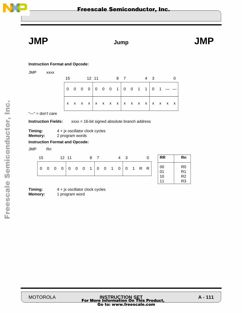
F
ree
sca
le S
em
ico
nd
uc
tor,
I
Freescale Semiconductor, Inc.n
c..
.
Instruction Format and Opcode:
JMP xxxx
“—” = don’t care
Instruction Fields: xxxx = 16-bit signed absolute branch address
Timing: 4 + jx oscillator clock cyclesMemory: 2 program words
Instruction Format and Opcode:
JMP Rn
Timing: 4 + jx oscillator clock cyclesMemory: 1 program word
JMP Jump JMP
x x x x x x x x x x x x x x x x
0 0 0 0 0 0 0 1 0 0 1 1 0 1 — —
15 12 11 8 7 4 3 0
0 0 0 0 0 0 0 1 0 0 1 0 0 1 R R
15 12 11 8 7 4 3 0 RR Rn
00 R001 R110 R211 R3
MOTOROLA INSTRUCTION SET A - 111 For More Information On This Product,
Go to: www.freescale.com
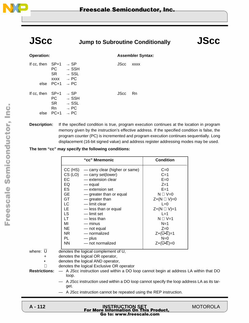
F
ree
sca
le S
em
ico
nd
uc
tor,
I
Freescale Semiconductor, Inc.n
c..
.
Operation: Assembler Syntax:
If cc, then SP+1 → SP JScc xxxxPC → SSHSR → SSLxxxx → PC
else PC+1 → PC
If cc, then SP+1 → SP JScc RnPC → SSHSR → SSLRn → PC
else PC+1 → PC
Description: If the specified condition is true, program execution continues at the location in programmemory given by the instruction’s effective address. If the specified condition is false, theprogram counter (PC) is incremented and program execution continues sequentially. Longdisplacement (16-bit signed value) and address register addressing modes may be used.
The term “cc” may specify the following conditions:
where: U denotes the logical complement of U,+ denotes the logical OR operator,• denotes the logical AND operator,⊕ denotes the logical Exclusive OR operator
Restrictions: — A JScc instruction used within a DO loop cannot begin at address LA within that DOloop.
— A JScc instruction used within a DO loop cannot specify the loop address LA as its tar-get.
— A JScc instruction cannot be repeated using the REP instruction.
JScc Jump to Subroutine Conditionally JScc
“cc” Mnemonic Condition
CC (HS) — carry clear (higher or same) C=0CS (LO) — carry set(lower) C=1EC — extension clear E=0EQ — equal Z=1ES — extension set E=1GE — greater than or equal N ⊕ V=0GT — greater than Z+(N ⊕ V)=0LC — limit clear L=0LE — less than or equal Z+(N ⊕ V)=1LS — limit set L=1LT — less than N ⊕ V=1MI — minus N=1NE — not equal Z=0NR — normalized Z+(U•E)=1PL — plus N=0NN — not normalized Z+(U•E)=0
A - 112 INSTRUCTION SET MOTOROLA For More Information On This Product,
Go to: www.freescale.com

F
ree
sca
le S
em
ico
nd
uc
tor,
I
Freescale Semiconductor, Inc.n
c..
.
Example:
JSLS R2 ;jump to subroutine at P:(R2) if limit set
Explanation of Example: In this example, program execution is transferred to the subroutine at addressP:(R2) if the limit bit is set. If the specified condition is not true, no jump is taken and theprogram counter is incremented by one.
Condition Codes Affected: The condition codes are not affected by this instruction.
Instruction Format and Opcode:
JScc xxxx
“—” = don’t careInstruction Fields: xxxx = 16-bit absolute branch address
Timing: 4 + jx oscillator clock cyclesMemory: 2 program words
Instruction Format and Opcode:
JScc Rn
Timing: 4 + jx oscillator clock cyclesMemory: 1 program word
Instruction Fields:cc = 4-bit condition code = cccc
JScc Jump to Subroutine Conditionally JScc
x x x x x x x x x x x x x x x x
0 0 0 0 0 1 1 0 — — 0 1 c c c c
15 12 11 8 7 4 3 0
0 0 0 0 0 1 1 0 R R 0 0 c c c c
15 12 11 8 7 4 3 0 RR Rn
00 R001 R110 R211 R3
Mnemonic c c c c
CC(HS) 0 0 0 0GE 0 0 0 1NE 0 0 1 0PL 0 0 1 1NN 0 1 0 0EC 0 1 0 1LC 0 1 1 0GT 0 1 1 1
Mnemonic c c c c
CS(LO) 1 0 0 0LT 1 0 0 1EQ 1 0 1 0MI 1 0 1 1NR 1 1 0 0ES 1 1 0 1LS 1 1 1 0LE 1 1 1 1
MOTOROLA INSTRUCTION SET A - 113 For More Information On This Product,
Go to: www.freescale.com

F
ree
sca
le S
em
ico
nd
uc
tor,
I
Freescale Semiconductor, Inc.n
c..
.
Operation: Assembler Syntax:
SP+1 → SP JSR xxxxPC → SSHSR → SSLxxxx → PC
SP+1 → SP JSR AAPC → SSHSR → SSLAA → PC
SP+1 → SP JSR RnPC → SSHSR → SSLRn → PC
Description: Jump to subroutine in program memory at the location given by the instruction’s effectiveaddress. Short displacement (8 bit unsigned value), long displacement (16-bit absoluteaddress) and address register addressing modes may be used.
Restrictions: — A JSR instruction used within a DO loop cannot begin at address LA within that DOloop.
— A JSR instruction used within a DO loop cannot specify the loop address LA as its tar-get.
— A JSR instruction cannot be repeated using the REP instruction.
Example:
JSR R2 ;jump to absolute address pointed to by R2
Explanation of Example: In this example, program execution is transferred the subroutine at addressP:(R2)
Condition Codes Affected:
The condition codes are not affected by this instruction.
JSR Jump to Subroutine JSR
A - 114 INSTRUCTION SET MOTOROLA For More Information On This Product,
Go to: www.freescale.com
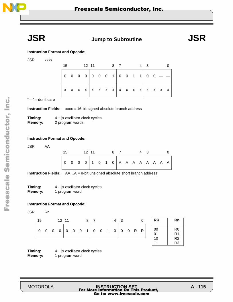
F
ree
sca
le S
em
ico
nd
uc
tor,
I
Freescale Semiconductor, Inc.n
c..
.
Instruction Format and Opcode:
JSR xxxx
“—” = don’t care
Instruction Fields: xxxx = 16-bit signed absolute branch address
Timing: 4 + jx oscillator clock cyclesMemory: 2 program words
Instruction Format and Opcode:
JSR AA
Instruction Fields: AA…A = 8-bit unsigned absolute short branch address
Timing: 4 + jx oscillator clock cyclesMemory: 1 program word
Instruction Format and Opcode:
JSR Rn
Timing: 4 + jx oscillator clock cyclesMemory: 1 program word
JSR Jump to Subroutine JSR
x x x x x x x x x x x x x x x x
0 0 0 0 0 0 0 1 0 0 1 1 0 0 — —
15 12 11 8 7 4 3 0
0 0 0 0 1 0 1 0 A A A A A A A A
15 12 11 8 7 4 3 0
0 0 0 0 0 0 0 1 0 0 1 0 0 0 R R
15 12 11 8 7 4 3 0 RR Rn
00 R001 R110 R211 R3
MOTOROLA INSTRUCTION SET A - 115 For More Information On This Product,
Go to: www.freescale.com

Fre
esc
ale
Se
mic
on
du
cto
r, I
Freescale Semiconductor, Inc.n
c..
.
Operation: Assembler Syntax:
ea → D (no parallel move) LEA ea,D
Description: The address calculation specified is executed and the resulting effective address is storedin the destination register. The source address register and the update mode used to com-pute the updated address are specified by the effective address (ea). Note that the sourceaddress register specified in the effective address is not updated. All update addressingmodes may be used.
Note: This instruction is considered to be a move-type instruction. Due to pipelining, the new contents ofthe destination address register (R0-R3 or N0-N3) will not be available for use during the following instruc-tion (i.e., there is a single instruction cycle pipeline delay).
Example:
LEA (R0)+N0,R1 ;update R1 using (R0)+N0
Explanation of Example: Prior to execution, the 16-bit address register R0 contains the value $0003, the16-bit address register N0 contains the value $0005 and the 16-bit address register R1 con-tains the value $0004. Execution of the LEA (R0)+N0,R1 instruction adds the contents ofthe R0 register to the contents of the N0 register and stores the resulting updated addressin the R1 address register. The contents of both the R0 and N0 address registers are notaffected.
Condition Codes Affected:
The condition codes are not affected by this instruction.
LEA Load Effective Address LEA
R1 0004
N0 0005
Before Execution
R0 0003
R1 0008
N0 0005
After Execution
R0 0003
A - 116 INSTRUCTION SET MOTOROLA For More Information On This Product,
Go to: www.freescale.com
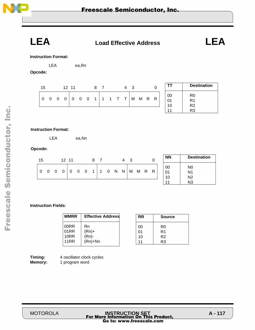
Fre
esc
ale
Se
mic
on
du
cto
r, I
Freescale Semiconductor, Inc.n
c..
.
Instruction Format:
LEA ea,Rn
Opcode:
Instruction Fields:
Timing: 4 oscillator clock cyclesMemory: 1 program word
LEA Load Effective Address LEA
0 0 0 0 0 0 0 1 1 1 T T M M R R
15 12 11 8 7 4 3 0
0 0 0 0 0 0 0 1 1 0 N N M M R R
15 12 11 8 7 4 3 0
TT Destination
00 R001 R110 R211 R3
NN Destination
00 N001 N110 N211 N3
Instruction Format:
LEA ea,Nn
Opcode:
MMRR Effective Address
00RR Rn01RR (Rn)+10RR (Rn)-11RR (Rn)+Nn
RR Source
00 R001 R110 R211 R3
MOTOROLA INSTRUCTION SET A - 117 For More Information On This Product,
Go to: www.freescale.com

Fre
esc
ale
Se
mic
on
du
cto
r, I
Freescale Semiconductor, Inc.n
c..
.
Assembler Syntax:
LSL D (parallel move)
Operation:
Description: Logically shift bits 31-16 (D1) of the destination operand D one bit to the left and store theresult in the destination accumulator upper word D1. The MS bit of D1 (bit 31 of D) is shiftedinto the carry bit C prior to instruction execution and a zero is shifted into the LS bit of theD1 (bit 16 of D).
Example:
LSL A (R3)- ;multiply A1 by 2, update R3
Explanation of Example: Prior to execution, the 40-bit A accumulator contains the value $A5:8123:0123.Execution of the LSL A instruction shifts the16-bit value in the A1 accumulator one bit tothe left and leaves A2 and A1 unchanged. The C bit of CCR (bit 0) is set by the operationbecause bit 31 of A was set prior to the instruction execution.
LSL Logical Shift Left LSL
unch. unchanged 0 (parallel move)
D2 D1 D0
C
0000
SR=MR:CCR
0001
SR=MR:CCR
After Execution
A5 0246 0123
A2 A1 A0
Before Execution
A5 8123 0123
A2 A1 A0
A - 118 INSTRUCTION SET MOTOROLA For More Information On This Product,
Go to: www.freescale.com

Fre
esc
ale
Se
mic
on
du
cto
r, I
Freescale Semiconductor, Inc.n
c..
.
Condition Codes Affected:
S — Computed according to the standard definition (see section A.4)L — Set if limiting (parallel move) or overflow has occurred in resultN — Set if bit 31 of A or B result is setZ — Set if A1 or B1 result equals zeroV — Always clearedC — Set if bit 31 of A or B was set prior to instruction execution
Instruction Format:
LSL D (parallel move)
Opcode:
Instruction Fields: Please see the “X Memory Data Move” description in the parallel move section for details on the m, RR, HHH, and W data fields.
Timing: 2 + mv oscillator clock cyclesMemory: 1 program word
LSL Logical Shift Left LSL
15 14 13 12 11 10 9 8 7 6 5 4 3 2 1 0
LF * * * S1 S0 I1 I0 S L E U N Z V C
CCRMR
1 m R R H H H W 0 0 1 1 F 0 1 1
15 12 11 8 7 4 3 0
D F
A 0B 1
MOTOROLA INSTRUCTION SET A - 119 For More Information On This Product,
Go to: www.freescale.com

Fre
esc
ale
Se
mic
on
du
cto
r, I
Freescale Semiconductor, Inc.n
c..
.
Assembler Syntax:
LSR D (parallel move)
Operation:
Description: Logically shift bits 31-16 (D1) of the destination operand D one bit to the right and store theresult in the destination accumulator upper word D1. The LS bit of D1 (bit 16 of D) prior toinstruction execution is shifted into the carry bit C and zero is shifted into the MS bit of D1(bit31 of D).
Example:
:LSR B X:-(R3),R3 ;divide B1 by 2, update R3, load R3
Explanation of Example: Prior to execution, the 40-bit B accumulator contains the value$A8:0001:A865. Execution of the LSR B instruction shifts the 16-bit value in the B1 registerone bit to the right and stores the result back in the B1 register. The C bit of CCR (bit 0) isset by the operation because bit 0 of A1 was set prior to the instruction execution. The Z bitof CCR (bit 2) is also set because the result in A1 is zero.
LSR Logical Shift Right LSR
0
unch. unchanged C (parallel move)
D2 D1 D0
0300
SR=MR:CCR
0305
SR=MR:CCR
After Execution
A8 0000 A865
B2 B1 B0
Before Execution
A8 0001 A865
B2 B1 B0
A - 120 INSTRUCTION SET MOTOROLA For More Information On This Product,
Go to: www.freescale.com
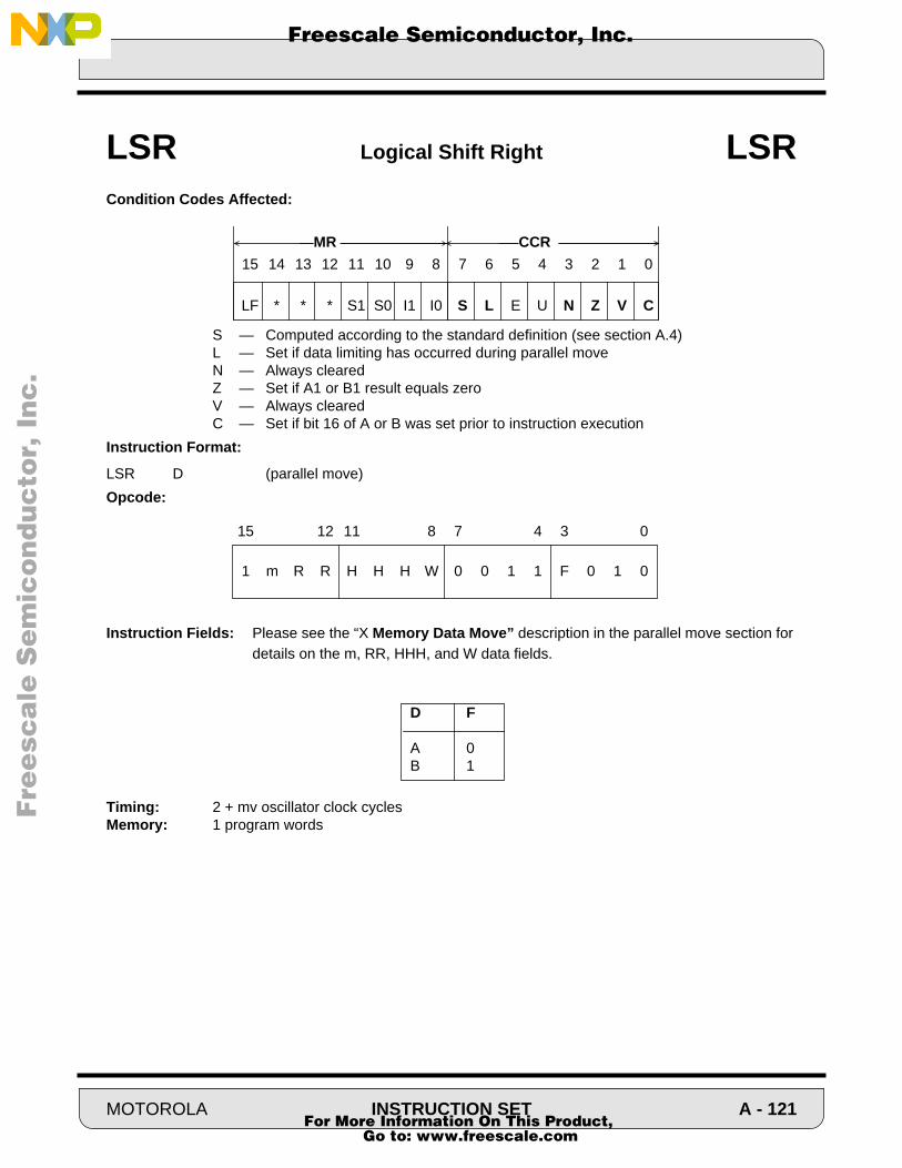
Fre
esc
ale
Se
mic
on
du
cto
r, I
Freescale Semiconductor, Inc.n
c..
.
Condition Codes Affected:
S — Computed according to the standard definition (see section A.4)L — Set if data limiting has occurred during parallel moveN — Always clearedZ — Set if A1 or B1 result equals zeroV — Always clearedC — Set if bit 16 of A or B was set prior to instruction execution
Instruction Format:
LSR D (parallel move)
Opcode:
Instruction Fields: Please see the “X Memory Data Move” description in the parallel move section for details on the m, RR, HHH, and W data fields.
Timing: 2 + mv oscillator clock cyclesMemory: 1 program words
LSR Logical Shift Right LSR
15 14 13 12 11 10 9 8 7 6 5 4 3 2 1 0
LF * * * S1 S0 I1 I0 S L E U N Z V C
CCRMR
1 m R R H H H W 0 0 1 1 F 0 1 0
15 12 11 8 7 4 3 0
D F
A 0B 1
MOTOROLA INSTRUCTION SET A - 121 For More Information On This Product,
Go to: www.freescale.com
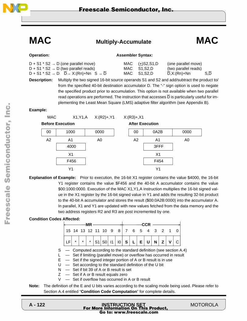
Fre
esc
ale
Se
mic
on
du
cto
r, I
Freescale Semiconductor, Inc.n
c..
.
Operation: Assembler Syntax:
D + S1 * S2 → D (one parallel move) MAC (+)S2,S1,D (one parallel move)D + S1 * S2 → D (two parallel reads) MAC S1,S2,D (two parallel reads)D + S1 * S2 → D D→ X:(Rn)+Nn S → D MAC S1,S2,D D,X:(Rn)+Nn S,D
Description: Multiply the two signed 16-bit source operands S1 and S2 and add/subtract the product to/from the specified 40-bit destination accumulator D. The “-” sign option is used to negatethe specified product prior to accumulation. This option is not available when two parallelread operations are performed. The instruction that accesses D is particularly useful for im-plementing the Least Mean Square (LMS) adaptive filter algorithm (see Appendix B).
Example:
MAC X1,Y1,A X:(R2)+,Y1 X:(R3)+,X1
Explanation of Example: Prior to execution, the 16-bit X1 register contains the value $4000, the 16-bitY1 register contains the value $F456 and the 40-bit A accumulator contains the value$00:1000:0000. Execution of the MAC X1,Y1,A instruction multiplies the 16-bit signed val-ue in the X1 register by the 16-bit signed value in Y1 and adds the resulting 32-bit productto the 40-bit A accumulator and stores the result ($00:0A2B:0000) into the accumulator A.In parallel, X1 and Y1 are updated with new values fetched from the data memory and thetwo address registers R2 and R3 are post incremented by one.
Condition Codes Affected:
S — Computed according to the standard definition (see section A.4)L — Set if limiting (parallel move) or overflow has occurred in resultE — Set if the signed integer portion of A or B result is in useU — Set according to the standard definition of the U bitN — Set if bit 39 of A or B result is setZ — Set if A or B result equals zeroV — Set if overflow has occurred in A or B result
Note: The definition of the E and U bits varies according to the scaling mode being used. Please refer toSection A.4 entitled “Condition Code Computation” for complete details.
MAC Multiply-Accumulate MAC
4000
X1
After Execution
00 0A2B 0000
A2 A1 A0
Before Execution
00 1000 0000
A2 A1 A0
3FFF
X1
F456
Y1
F454
Y1
15 14 13 12 11 10 9 8 7 6 5 4 3 2 1 0
LF * * * S1 S0 I1 I0 S L E U N Z V C
CCRMR
A - 122 INSTRUCTION SET MOTOROLA For More Information On This Product,
Go to: www.freescale.com

Fre
esc
ale
Se
mic
on
du
cto
r, I
Freescale Semiconductor, Inc.n
c..
.
Timing: 2 + mv oscillator clock cyclesMemory: 1 program word
MAC Multiply-Accumulate MAC
1 m R R H H H W 1 k 1 0 F Q Q Q
15 12 11 8 7 4 3 0
0 1 1 m m K K K 1 x x 0 F 1 Q Q
15 12 11 8 7 4 3 0
0 0 0 1 0 1 1 1 R R D D F Q Q Q
15 12 11 8 7 4 3 0
Sign k+ 0- 1
Instruction Format: MAC S1,S2,D D,X:(Rn)+Nn S,D (one memory write, Opcode: one data register move)
Instruction Format: MAC S1,S2,D (two parallel reads)Opcode:
Instruction Format: MAC (+)S2,S1,D (one parallel move)Opcode:
Instruction Fields: Please see the “X Memory Data Write and Register Data Move” description in the parallel move section for details on the RR and DD data fields.
Instruction Fields: Please see the “Dual X Memory Data Read” description in the parallel move sec-tion for details on the mm and KKK data fields.
Instruction Fields: Please see the “X Memory Data Move” description in the parallel move section for details on the m, RR, HHH, and W data fields.
S1,S2,D QQQ FY0,X0,A 1 0 0 0Y0,X0,B 1 0 0 1Y1,X0,A 1 0 1 0Y1,X0,B 1 0 1 1Y0,X1,A 1 1 0 0Y0,X1,B 1 1 0 1Y1,X1,A 1 1 1 0Y1,X1,B 1 1 1 1
S1,S2,D QQQ FX0,X0,A 0 0 0 0X0,X0,B 0 0 0 1X1,X0,A 0 0 1 0X1,X0,B 0 0 1 1A1,Y0,A 0 1 0 0A1,Y0,B 0 1 0 1B1,X0,A 0 1 1 0B1,X0,B 0 1 1 1
One Or Two Parallel Operation Two Parallel ReadsS1,S2,D QQ FX1,Y0,A 1 0 0X1,Y0,B 1 0 1X1,Y1,A 1 1 0X1,Y1,B 1 1 1
S1,S2,D QQ FX0,Y0,A 0 0 0X0,Y0,B 0 0 1X0,Y1,A 0 1 0X0,Y1,B 0 1 1
MOTOROLA INSTRUCTION SET A - 123 For More Information On This Product,
Go to: www.freescale.com

F
ree
sca
le S
em
ico
nd
uc
tor,
I
Freescale Semiconductor, Inc.n
c..
.
Operation: Assembler Syntax:
D + S1 * S2 + r → D (one parallel move) MACR (+)S2,S1,D (one parallel operation)D + S1 * S2 + r → D (two parallel reads) MACR S1,S2,D (two parallel reads)
Description: Multiply the two signed 16-bit source operands S1 and S2, add/subtract the product to/fromthe specified 40-bit destination accumulator D, and round the result using the specifiedrounding. The rounded result is stored in the destination accumulator. Refer to the roundinstruction for more complete information on the convergent rounding process. The “-” signoption is used to negate the specified product prior to accumulation. This option is not avail-able when two parallel reads are performed. The default sign option is “+”.
Example:
MACR -X0,Y1,A A0,X0
Explanation of Example: Prior to execution, the 16-bit X0 register contains the value $4000 (0.5), the 16-bit Y1 register contains the value $F456 (-0.0911255) and the 40-bit A accumulator con-tains the value $00:1000:1234 (0.125002169981599). Execution of the MACR-X0,Y1,A in-struction multiplies the 16-bit signed value in the X0 register by the 16-bit signed value inY1 and substracts the resulting 32-bit product to the 40-bit A accumulator, rounds the resultand stores the result ($00:15D5:0000) into the accumulator A (-X0 * Y1 + A =0.170562744140625). In parallel, A0 is saved into X0 before the result is stored in A. In thisexample, the default rounding (convergent rounding) is performed.
MACR Multiply-Accumulate and Round MACR
4000
X0
After Execution
00 15D5 0000
A2 A1 A0
Before Execution
00 1000 1234
A2 A1 A0
1234
X0
F456
Y1
F454
Y1
A - 124 INSTRUCTION SET MOTOROLA For More Information On This Product,
Go to: www.freescale.com
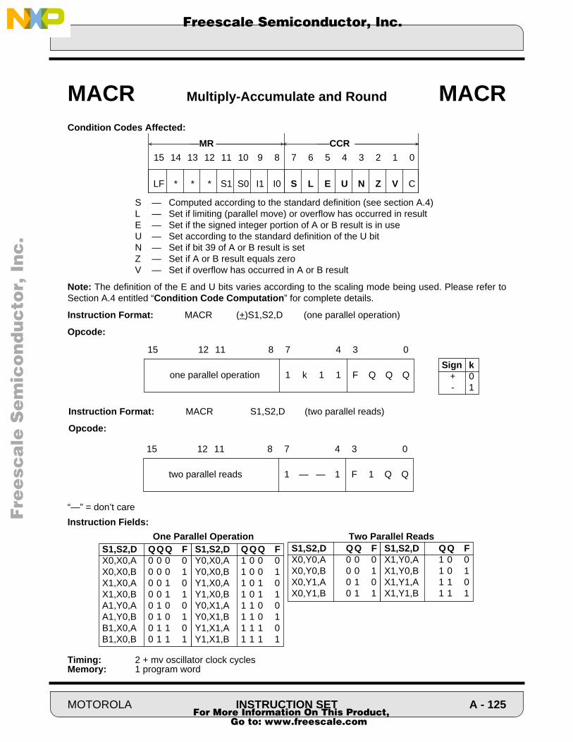
F
ree
sca
le S
em
ico
nd
uc
tor,
I
Freescale Semiconductor, Inc.n
c..
.
Condition Codes Affected:
S — Computed according to the standard definition (see section A.4)L — Set if limiting (parallel move) or overflow has occurred in resultE — Set if the signed integer portion of A or B result is in useU — Set according to the standard definition of the U bitN — Set if bit 39 of A or B result is setZ — Set if A or B result equals zeroV — Set if overflow has occurred in A or B result
Note: The definition of the E and U bits varies according to the scaling mode being used. Please refer toSection A.4 entitled “Condition Code Computation” for complete details.
Instruction Format: MACR (+)S1,S2,D (one parallel operation)
Opcode:
“—” = don’t care
Instruction Fields:
Timing: 2 + mv oscillator clock cyclesMemory: 1 program word
MACR Multiply-Accumulate and Round MACR
15 14 13 12 11 10 9 8 7 6 5 4 3 2 1 0
LF * * * S1 S0 I1 I0 S L E U N Z V C
CCRMR
one parallel operation 1 k 1 1 F Q Q Q
15 12 11 8 7 4 3 0
two parallel reads 1 — — 1 F 1 Q Q
15 12 11 8 7 4 3 0
Sign k+ 0- 1
Instruction Format: MACR S1,S2,D (two parallel reads)
Opcode:
One Parallel Operation Two Parallel ReadsS1,S2,D QQ FX1,Y0,A 1 0 0X1,Y0,B 1 0 1X1,Y1,A 1 1 0X1,Y1,B 1 1 1
S1,S2,D QQ FX0,Y0,A 0 0 0X0,Y0,B 0 0 1X0,Y1,A 0 1 0X0,Y1,B 0 1 1
S1,S2,D QQQ FY0,X0,A 1 0 0 0Y0,X0,B 1 0 0 1Y1,X0,A 1 0 1 0Y1,X0,B 1 0 1 1Y0,X1,A 1 1 0 0Y0,X1,B 1 1 0 1Y1,X1,A 1 1 1 0Y1,X1,B 1 1 1 1
S1,S2,D QQQ FX0,X0,A 0 0 0 0X0,X0,B 0 0 0 1X1,X0,A 0 0 1 0X1,X0,B 0 0 1 1A1,Y0,A 0 1 0 0A1,Y0,B 0 1 0 1B1,X0,A 0 1 1 0B1,X0,B 0 1 1 1
MOTOROLA INSTRUCTION SET A - 125 For More Information On This Product,
Go to: www.freescale.com
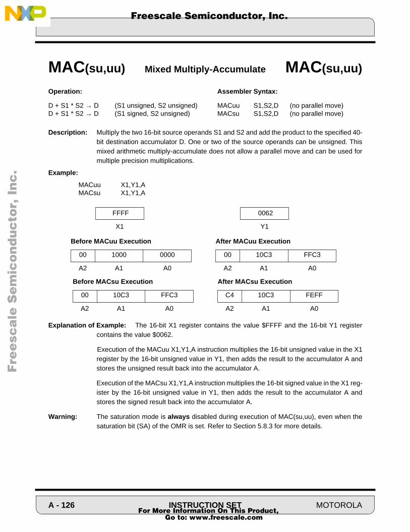
F
ree
sca
le S
em
ico
nd
uc
tor,
I
Freescale Semiconductor, Inc.n
c..
.
Operation: Assembler Syntax:
D + S1 * S2 → D (S1 unsigned, S2 unsigned) MACuu S1,S2,D (no parallel move)D + S1 * S2 → D (S1 signed, S2 unsigned) MACsu S1,S2,D (no parallel move)
Description: Multiply the two 16-bit source operands S1 and S2 and add the product to the specified 40-bit destination accumulator D. One or two of the source operands can be unsigned. Thismixed arithmetic multiply-accumulate does not allow a parallel move and can be used formultiple precision multiplications.
Example:
MACuu X1,Y1,AMACsu X1,Y1,A
Explanation of Example: The 16-bit X1 register contains the value $FFFF and the 16-bit Y1 registercontains the value $0062.
Execution of the MACuu X1,Y1,A instruction multiplies the 16-bit unsigned value in the X1register by the 16-bit unsigned value in Y1, then adds the result to the accumulator A andstores the unsigned result back into the accumulator A.
Execution of the MACsu X1,Y1,A instruction multiplies the 16-bit signed value in the X1 reg-ister by the 16-bit unsigned value in Y1, then adds the result to the accumulator A andstores the signed result back into the accumulator A.
Warning: The saturation mode is always disabled during execution of MAC(su,uu), even when thesaturation bit (SA) of the OMR is set. Refer to Section 5.8.3 for more details.
MAC(su,uu) Mixed Multiply-Accumulate MAC(su,uu)
FFFF
X1
After MACuu Execution
00 10C3 FFC3
A2 A1 A0
Before MACuu Execution
00 1000 0000
A2 A1 A0
0062
Y1
After MACsu Execution
C4 10C3 FEFF
A2 A1 A0
Before MACsu Execution
00 10C3 FFC3
A2 A1 A0
A - 126 INSTRUCTION SET MOTOROLA For More Information On This Product,
Go to: www.freescale.com

F
ree
sca
le S
em
ico
nd
uc
tor,
I
Freescale Semiconductor, Inc.n
c..
.
Condition Codes Affected:
E — Set if the signed integer portion of A or B result is in useU — Set according to the standard definition of the U bitN — Set if bit 39 of A or B result is setZ — Set if A or B result equals zeroV — Set if overflow has occurred in A or B result
Note: The definition of the E and U bits varies according to the scaling mode being used. Please refer toSection A.4 entitled “Condition Code Computation” for complete details.
Instruction Format:
MAC(uu) S1,S2,DMAC(su) S1,S2,D
Opcode:
Instruction Fields:
Timing: 2 oscillator clock cyclesMemory: 1 program word
MAC(su,uu) Mixed Multiply-Accumulate MAC(su,uu)
15 14 13 12 11 10 9 8 7 6 5 4 3 2 1 0
LF * * * S1 S0 I1 I0 S L E U N Z V C
CCRMR
0 0 0 1 0 1 0 1 1 1 1 0 F s Q Q
15 12 11 8 7 4 3 0
Arithmetic s
su 0 uu 1
S1,S2,D QQ FX1,Y0,A 1 0 0X1,Y0,B 1 0 1X1,Y1,A 1 1 0X1,Y1,B 1 1 1
S1,S2,D QQ FY0,X0,A 0 0 0Y0,X0,B 0 0 1Y1,X0,A 0 1 0Y1,X0,B 0 1 1
Note: For MACsu, the order of S1, S2 is sig-nificant; the signed value will be taken fromS1 while the unsigned value will be takenfrom S2.
MOTOROLA INSTRUCTION SET A - 127 For More Information On This Product,
Go to: www.freescale.com

F
ree
sca
le S
em
ico
nd
uc
tor,
I
Freescale Semiconductor, Inc.n
c..
.
Operation: Assembler Syntax:
one move MOVE (one parallel operation)two memory reads MOVE (double memory read)one parallel memory move plus MOVE (memory access, register move)one data register move#xxxx → D (see Move(C) instruction) MOVE #xxxx,D
Description: This instruction is equivalent to a Data ALU NOP with a parallel data move as described inSection A.4 entitled “Parallel Move Descriptions”. Refer to that section for more informa-tion.
When a 40-bit accumulator (A or B) is specified as a source operand S, the accumulatorvalue is optionally shifted according to the scaling mode bits S0 and S1 in the system statusregister (SR). If the data out of the shifter indicates that the accumulator extension registeris in use and the data is to be moved into a 16-bit destination, the value stored in the des-tination D is limited to a maximum positive or negative saturation constant to minimize trun-cation error. Limiting does not occur if an individual 16-bit accumulator register (A1, A0, B1,or B0) is specified as a source operand instead of the full 40-bit accumulator (A or B). Thislimiting feature allows block floating point operations to be performed with error detectionsince the L bit in the condition code register is latched (i.e., sticky).
When a 40-bit accumulator (A or B) is specified as a destination operand D, any 16-bitsource data to be moved into that accumulator is automatically extended to 40 bits by sign-extending the MS bit of the source operand (bit 15) and appending the source operand with16 LS zeros. Note that the automatic sign-extension and zeroing features may be circum-vented by specifying the destination register to be one of the individual 16-bit accumulatorregisters (A1 or B1).
Example:
MOVE X0,A1 ;move X0 to A1 without sign extension or zeroing
Explanation of Example: Prior to execution, the 40-bit A accumulator contains the value$FF:FFFF:FFFF and the 16-bit X0 register contains the value $1234. Execution of theMOVE X0,A1 instruction moves the 16-bit value in the X0 register into the 16-bit A1 registerwithout automatic sign extension and without automatic zeroing.
MOVE Move Data MOVE
After Last Execution
FF 1234 FFFF
A2 A1 A0
Before Last Execution
FF FFFF FFFF
A2 A1 A0
1234
X0
1234
X0
A - 128 INSTRUCTION SET MOTOROLA For More Information On This Product,
Go to: www.freescale.com

F
ree
sca
le S
em
ico
nd
uc
tor,
I
Freescale Semiconductor, Inc.n
c..
.
Condition Codes Affected:
S — Set according to standard definition of the S bit.L — Set if data limiting has occurred during parallel move
Instruction Format and Opcode:
MOVE (one parallel move)
Instruction Format and Opcode:
MOVE (double memory read)
Instruction Fields: Please see the “X Memory Data Move” description in the parallel move section for details on the m, RR, HHH, and W data fields. See the “Dual X Memory Read” de-scription in the parallel move section for details on the mm, KKK, and rr data fields.
Timing: 2 + mv oscillator clock cyclesMemory: 1 program word
Instruction Format and Opcode:
MOVE X:(R2+xx),D ;for W=0 -or- MOVE S,X:(R2+xx) ;for W=1
“—” = don’t care
Instruction Fields: Please see the “X Memory Data Move” description in the parallel move section for details on the HHH and W data fields.
Timing: 2 + mv oscillator clock cyclesMemory: 2 program words
MOVE Move Data MOVE
15 14 13 12 11 10 9 8 7 6 5 4 3 2 1 0
LF * * * S1 S0 I1 I0 S L E U N Z V C
CCRMR
1 m R R H H H W 0 0 0 1 0 0 0 1
15 12 11 8 7 4 3 0
0 1 1 m m K K K 0 r r 1 0 0 0 0
15 12 11 8 7 4 3 0
— — — — H H H W 0 0 0 1 0 0 0 1
0 0 0 0 0 1 0 1 B B B B B B B B
15 12 11 8 7 4 3 0
MOTOROLA INSTRUCTION SET A - 129 For More Information On This Product,
Go to: www.freescale.com

F
ree
sca
le S
em
ico
nd
uc
tor,
I
Freescale Semiconductor, Inc.n
c..
.
Thirty two Data ALU instructions provide the capability of specifying an optional parallel operation. This par-allel operation can be a data bus movement over the X Data Bus with optional address register update, anaddress register update without data bus movement or a Data ALU register transfer.
Eight major Data ALU instructions provide the capability of dual X memory read with address register up-date. These Data ALU instructions have been selected for optimal performance on frequently used DSPalgorithm critical loops.
Two Data ALU instructions, MPY and MAC, provide the capability of one parallel X memory read plus oneData ALU register transfer. These two instructions allow for very high performance adaptive transversal fil-tering.
Seven types of parallel moves are permitted, including register to register moves, register to memory movesand memory to register moves. However, not all addressing modes are allowed for each type of memoryreference. Addressing mode restrictions which apply to specific types of moves are noted in the individualmove operation descriptions. The following section contains detailed descriptions about each type of paral-lel move operation.
The symbols used in decoding the various opcode fields of an instruction or parallel move are completelyarbitrary. Furthermore, the opcode symbols used in one instruction or parallel move are completely inde-pendent of the opcode symbols used in a different instruction or parallel move.
Parallel Move DescriptionsParallelMove
ParallelMove
A - 130 INSTRUCTION SET MOTOROLA For More Information On This Product,
Go to: www.freescale.com

F
ree
sca
le S
em
ico
nd
uc
tor,
I
Freescale Semiconductor, Inc.n
c..
.
Operation: Assembler Syntax:
(…) (…)where (…) refers to any arithmetic or logical instruction.
Description: All Data ALU operations can be performed without any parallel move.
Example:
:ADD X0,A ;add X0 to A (no parallel move)
:
Explanation of Example: This is an example of an instruction which allows parallel moves but doesn’t have one.
Condition Codes Affected:The condition codes are not affected by this type of parallel move.
Instruction Format:
(…)
Opcode:
Instruction Fields: (defined by Data ALU instruction)
Timing: mv oscillator clock cyclesMemory: mv program words
No Parallel Data MoveParallelMove
ParallelMove
0 1 0 0 1 0 1 0 Data ALU Opcode
15 12 11 8 7 4 3 0
MOTOROLA INSTRUCTION SET A - 131 For More Information On This Product,
Go to: www.freescale.com
F
ree
sca
le S
em
ico
nd
uc
tor,
I
Freescale Semiconductor, Inc.n
c..
.
Operation: Assembler Syntax:
S → D (…) S,D (…);
where (…) refers to any arithmetic or logical instruction which allows parallel moves.
Description: Move the source register S to the destination register D.
If the arithmetic or logical opcode-operand portion of the instruction specifies a given destination accumu-lator, that same accumulator or portion of that accumulator may not be specified as a destination D in theparallel data bus move operation. Thus, if the opcode-operand portion of the instruction specifies the 40-bitA accumulator as its destination, the parallel data bus move portion of the instruction may not specify A0,A1, A2, or A as its destination D. Similarly, if the opcode-operand portion of the instruction specifies the 40-bit B accumulator as its destination, the parallel data bus move portion of the instruction may not specify B0,B1, B2, or B as its destination D. That is, duplicate destinations are not allowed within the same instruction.
If the opcode-operand portion of the instruction specifies a given source or destination register, that sameregister or portion of that register may be used as a source S in the parallel data bus move operation. Thisallows data to be moved in the same instruction in which it is being used as a source operand by a DataALU operation. That is, duplicate sources are allowed within the same instruction.
Note: The MOVE A,B operation will result in a 16-bit positive or negative saturation constant being storedin the B1 portion of the B accumulator if the signed integer portion of the A accumulator is in use.The opposite is true for the MOVE B,A instruction.
Example:
MACR -X0,Y0,B A,X1
Explanation of Example: Prior to execution, the 16-bit X1 register contains the value $0003 and the 40-bit accumulator A contains the value $01:0008:789A. Execution of the parallel move portionof the instruction, A,X1, moves the contents of A1 into the X1. Limiting is performed by theshifter limiter because the data stored in A before instruction execution is using the integerportion of A. The example assumes no scaling is selected in the MR register.
Register to Register Data MoveParallelMove
ParallelMove
0003
X1
After Execution
01 0008 789A
A2 A1 A0
Before Execution
01 0008 789A
A2 A1 A0
7FFF
X1
A - 132 INSTRUCTION SET MOTOROLA For More Information On This Product,
Go to: www.freescale.com

F
ree
sca
le S
em
ico
nd
uc
tor,
I
Freescale Semiconductor, Inc.n
c..
.
Condition Codes:
S — Set according to the standard definition of the S bit.L — Set if data limiting has occurred during parallel move
Instruction Format:
(…) S,D
Opcode:
Instruction Fields:
Timing: mv oscillator clock cyclesMemory: mv program words
Register to Register Data MoveParallelMove
ParallelMove
15 14 13 12 11 10 9 8 7 6 5 4 3 2 1 0
LF * * * S1 S0 I1 I0 S L E U N Z V C
CCRMR
0 1 0 0 I I I I Data ALU Opcode
15 12 11 8 7 4 3 0
S,D I I I I
X0,F 0000Y0,F 0001X1,F 0010Y1,F 0011A,X0 0100B,Y0 0101A0,X0 0110B0,Y0 0111F,F 1000F,F 1001A,X1 1100B,Y1 1101A0,X1 1110B0,Y1 1111
F is the accumulator which is not used by the parallel Data ALU operation.(in the case of no Data ALU operation, A is chosen)
MOTOROLA INSTRUCTION SET A - 133 For More Information On This Product,
Go to: www.freescale.com

F
ree
sca
le S
em
ico
nd
uc
tor,
I
Freescale Semiconductor, Inc.n
c..
.
Operation: Assembler Syntax:
(…); ea → Rn (…) ea
where (…) refers to any arithmetic or logical instruction which allows such parallel operations.
Description: Update the specified address register according to the specified effective addressingmode. Two update addressing modes may be used (postdecrement by one; postincrementby the offset register).
Example:
RND B (R3)+N3 ;round value in B into B1, R3+N3 → R3
Explanation of Example: Prior to execution, the 16-bit address register R3 contains the value $0007and the 16-bit address offset register N3 contains the value $0004. Execution of the parallelmove portion of the instruction, (R3)+N3, updates the R3 address register according to thespecified effective addressing mode by adding the value in the R3 register to the value inthe N3 register and storing the 16-bit result back in the R3 address register.
Condition Codes Affected:The condition codes are not affected by this type of parallel operation.
Address Register UpdateParallelMove
ParallelMove
Before Execution
R3 0007
After Execution
R3 000B
N3 0004 N3 0004
A - 134 INSTRUCTION SET MOTOROLA For More Information On This Product,
Go to: www.freescale.com

F
ree
sca
le S
em
ico
nd
uc
tor,
I
Freescale Semiconductor, Inc.n
c..
.
Instruction Format:
(…) ea
Opcode:
Instruction Fields:
Timing: mv oscillator clock cyclesMemory: mv program words
Address Register UpdateParallelMove
ParallelMove
0 0 1 1 0 z R R Data ALU Opcode
15 12 11 8 7 4 3 0
RR Rn
00 R001 R110 R211 R3
ea z
(Rn)- 0(Rn)+Nn 1
MOTOROLA INSTRUCTION SET A - 135 For More Information On This Product,
Go to: www.freescale.com

F
ree
sca
le S
em
ico
nd
uc
tor,
I
Freescale Semiconductor, Inc.n
c..
.
Operation: Assembler Syntax:
(…) X:<ea> → D (…) X:<ea>,D(…) S → X:<ea> (…) S,X:<ea>
where (…) refers to any arithmetic or logical instruction which allows parallel moves.
Description: Move the specified word operand from/to X memory. Two indirect addressing modes maybe used (postincrement by one and postincrement by the offset register) as well as a spe-cial addressing mode using the upper word of the accumulator which is not used by theData ALU operation.
If the arithmetic or logical opcode-operand portion of the instruction specifies a given destination accumu-lator, that same accumulator or portion of that accumulator may not be specified as a destination D in theparallel data bus move operation. Thus, if the opcode-operand portion of the instruction specifies the 40-bitA or B accumulator as its destination, the parallel data bus move portion of the instruction may not specifyA0/B0, A1/B1, A2/B2, or A/B as its destination D. That is, duplicate destinations are not allowed within thesame instruction.
Exceptions: — DEC24, INC24, CLR24, OR, AND, NOT, EOR, LSL, LSR, ROL, and ROR allow thelower portion of the accumulator (A0 or B0) to be the destination of the parallel moveeven if this accumulator is used by the Data ALU operation because these instructionsonly affect the MS 16 or 24 bits of the accumulator.
— TST, CMP, CMPM allow both the accumulator and its lower portion (A and A0, B andB0) to be the parallel move destination even if this accumulator is used by the Data ALUoperation. These instructions do not have a true destination.
If the opcode-operand portion of the instruction specifies a given source or destination register, that sameregister or portion of that register may be used as a source S in the parallel data bus move operation. Thisallows data to be moved in the same instruction in which it is being used as a source operand by a DataALU operation. That is, duplicate sources are allowed within the same instruction.
Example:
MOVE #$100,R2MOVE #4,X1ASL A X1,X:(R2)+ ; A*2 → A; save X1 in X:(R2); increment R2
Explanation of Example: Prior to execution, the 16-bit R2 address register contains the value $100and the 16-bit X memory location X:$0100 contains the value $0000. Execution of the parallel move portionof the instruction, X1,X:(R2)+ uses the R2 address register to move the contents of the X1 register into the16-bit X memory location X:$1000. R2 is then incremented by one.
X Memory Data MoveParallelMove
ParallelMove
Before Execution
R2 0100
After Execution
R2 0101
X:$100 0000 X:$100 0004
A - 136 INSTRUCTION SET MOTOROLA For More Information On This Product,
Go to: www.freescale.com

F
ree
sca
le S
em
ico
nd
uc
tor,
I
Freescale Semiconductor, Inc.n
c..
.
Condition Codes Affected:
S — Set according to the standard definition of the S bit.L — Set if data limiting has occurred during parallel move
Note: The MOVE A,X:<ea> or MOVE B,X:<ea> operation will result in a 16-bit positive or negative satu-ration constant being stored in the specified 16-bit X memory location if the signed integer portionof the A accumulator or B accumulator, respectively, is in use.
Instruction Format:
(…) X:<ea>,D(…) S,X:<ea>
Opcode and instruction Fields:
Timing: mv oscillator clock cycles Memory: 1 program word
Instruction Format:
(…) X:(F1),D(…) S,X:(F1)
Opcode and instruction Fields:
Timing: mv oscillator clock cycles Memory: mv program words
15 14 13 12 11 10 9 8 7 6 5 4 3 2 1 0
LF * * * S1 S0 I1 I0 S L E U N Z V C
CCRMR
X Memory Data MoveParallelMove
ParallelMove
1 m R R H H H W Data ALU Opcode
15 12 11 8 7 4 3 0
Reg. Wread S 0write D 1
HHH S,D HHH S,D
000 X0 100 A001 Y0 101 B010 X1 110 A0011 Y1 111 B0
ea m(Rn)+ 0(Rn)+Nn 1
where “RR” refers to an Address Register R0-R3
0 1 0 1 H H H W Data ALU Opcode
15 12 11 8 7 4 3 0
Reg. Wread S 0write D 1
HHH S,D HHH S,D
000 X0 100 A001 Y0 101 B010 X1 110 A0011 Y1 111 B0
F1 is the upper word of the accumulator which is not used by the parallel Data ALU operation
(in case of no Data ALU operation, A1 is chosen as F)
MOTOROLA INSTRUCTION SET A - 137 For More Information On This Product,
Go to: www.freescale.com

F
ree
sca
le S
em
ico
nd
uc
tor,
I
Freescale Semiconductor, Inc.n
c..
.
Operation: Assembler Syntax:
(…) X:(R2+xx) → D (…) X:(R2+xx),D(…) S → X:(R2+xx) (…) S,X:(R2+xx)
where (…) refers to any arithmetic or logical instruction which allows parallel moves.
Description: Move the specified word operand from/to X memory. The indirect addressing mode on R2indexed by a short (8 bits) signed displacement value is used. The 8-bit signed value is signextended to 16 bits before being added to R2. For example, X:(R2+$F0) and X:(R2-$10)will access the same memory location.
If the arithmetic or logical opcode-operand portion of the instruction specifies a given destination accumu-lator, that same accumulator or portion of that accumulator may not be specified as a destination D in theparallel data bus move operation. Thus, if the opcode-operand portion of the instruction specifies the 40-bitA accumulator as its destination, the parallel data bus move portion of the instruction may not specify A0,A1, A2, or A as its destination D. Similarly, if the opcode-operand portion of the instruction specifies the 40-bit B accumulator as its destination, the parallel data bus move portion of the instruction may not specify B0,B1, B2, or B as its destination D. That is, duplicate destinations are not allowed within the same instruction.
If the opcode-operand portion of the instruction specifies a given source or destination register, that sameregister or portion of that register may be used as a source S in the parallel data bus move operation. Thisallows data to be moved in the same instruction in which it is being used as a source operand by a DataALU operation. That is, duplicate sources are allowed within the same instruction.
Example:
MOVE #4,X1ASL A X1,X:(R2+$64) ; A*2 → A; save X1 in X:(R2+$64)
Explanation of Example: Prior to execution, the 16-bit R2 address register contains the value $100 and the 16-bit X memory location X:$0100 contains the value $0000. Execution of the parallel move portion of the instruction, X1,X:(R2+$64) moves the contents of the X1 register into the 16-bit X memory location X:$164. R2 is not affected by the instruction.
X Memory Data Move with short displacementParallelMove
ParallelMove
Before Execution
R2 0100
After Execution
R2 0100
X:$164 0000 X:$164 0004
A - 138 INSTRUCTION SET MOTOROLA For More Information On This Product,
Go to: www.freescale.com

F
ree
sca
le S
em
ico
nd
uc
tor,
I
Freescale Semiconductor, Inc.n
c..
.
Condition Codes Affected:
S — Set according to the standard definition of the S bit.L — Set if data limiting has occurred during parallel move
Note: The MOVE A,X:(R2+xx) or MOVE B,X:(R2+xx) operation will result in a 16-bit positive or negativesaturation constant being stored in the specified 16-bit X memory location if the signed integer por-tion of the A or B accumulator, respectively, is in use.
Instruction Format:
(…) X:(R2+xx),D(…) S,X:(R2+xx)
Opcode and instruction Fields:
“—” = don’t careBB…B = the 8-bit signed displacement
Timing: mv oscillator clock cycles
Memory: mv program words
15 14 13 12 11 10 9 8 7 6 5 4 3 2 1 0
LF * * * S1 S0 I1 I0 S L E U N Z V C
CCRMR
X Memory Data Move with short displacementParallelMove
ParallelMove
Reg. Wread S 0write D 1
HHH S,D HHH S,D
000 X0 100 A001 Y0 101 B010 X1 110 A0011 Y1 111 B0
— — — — H H H W Data ALU OPCODE
0 0 0 0 0 1 0 1 B B B B B B B B
15 12 11 8 7 4 3 0
MOTOROLA INSTRUCTION SET A - 139 For More Information On This Product,
Go to: www.freescale.com
F
ree
sca
le S
em
ico
nd
uc
tor,
I
Freescale Semiconductor, Inc.n
c..
.
Operation: Assembler Syntax:
(MPY or MAC) D → X:(Rn)+Nn S → D (MPY or MAC) D,X:(Rn)+Nn S,D
Description: In parallel with a MPY or a MAC, move the accumulator which is not used as a destinationby the MPY or MAC into the X memory location specified by the indirect postincrement byoffset addressing mode, and update this accumulator with the value contained in one of thefour Data ALU registers. This parallel memory move with register data move is optimizedfor adaptive digital transversal filtering.
Note: The X memory write operation will result in a 16-bit positive or negative saturation constant beingstored in the specified 16-bit X memory location if the signed integer portion of the A or B accumu-lator is in use.
Example:
MAC Y0,X1,B A,X:(R1)+N1 X1,A
Explanation of Example: Prior to execution, the 40-bit A accumulator contains the value $01:0008:789A, the 16-bit X memory location X:$(R1) contains the value $1234 and the 16-bit X1 register contains the value $0003. Execution of the parallel move portion of the instruction, A,X:(R1)+N1 X1,A moves the 16-bit limited positive saturation constant $7FFF into the X:(R1) memory location and then moves the contents of X1 into A. N1 is also added to R1.
Condition Codes Affected:
S — Computed according to the standard definitionL — Set if data limiting has occurred during parallel move
X Memory Data Write and Register Data MoveParallelMove
ParallelMove
0003
X1
After Execution
00 0003 0000
A2 A1 A0
Before Execution
01 0008 789A
A2 A1 A0
0003
X1
1234
X:(R1)
7FFF
X:(R1)
15 14 13 12 11 10 9 8 7 6 5 4 3 2 1 0
LF * * * S1 S0 I1 I0 S L E U N Z V C
CCRMR
A - 140 INSTRUCTION SET MOTOROLA For More Information On This Product,
Go to: www.freescale.com

F
ree
sca
le S
em
ico
nd
uc
tor,
I
Freescale Semiconductor, Inc.n
c..
.
Instruction Format:
(MPY or MAC) D,X:(Rn)+Nn S,D
Opcode and instruction Fields:
Timing: mv oscillator clock cyclesMemory: mv program words
X Memory Data Write and Register Data MoveParallelMove
ParallelMove
0 0 0 1 0 1 1 k R R D D Data ALU
15 12 11 8 7 4 3 0
D kB 0A 1
S DD
X0 00Y0 01X1 10Y1 11
where “RR” refers to an Address Register R0-R3
MOTOROLA INSTRUCTION SET A - 141 For More Information On This Product,
Go to: www.freescale.com
F
ree
sca
le S
em
ico
nd
uc
tor,
I
Freescale Semiconductor, Inc.n
c..
.
Operation: Assembler Syntax:
(…) X:<ea> → D1 X:<ea> → D2 (…) X:<ea>,D1 X:<ea>,D2
where (…) refers to a limited set of arithmetic instructions which allow double parallel reads (MOVE, MAC(R), MPY(R), ADD, SUB, TFR)
Description: Move two 16-bit word operands from X memory. Note that two independent effective ad-dresses can be specified where one of the effective addresses uses the Address Registers(R0-R2) while the other effective address must use address register R3. Two parallel ad-dressing modes may be used for each effective address. In that case, address update onR3 is only performed using linear arithmetic (the value of M3 is ignored). D1 and D2 maynot specify the same register since duplicate destinations are not allowed within the sameinstruction.
Note: The second X data memory parallel read never accesses on-chip peripherals. If the valueaddressed by R3 reaches the last 64 locations of the X data memory, external memory willbe accessed.
Example:
MPYR X1,Y0,A X:(R0)+,Y0 X:(R3)+N3,X1
Explanation of Example: Prior to execution, the 16-bit X1 register contains the value $0003, the 16-bit Y0 register contains the value $1234. Execution of the parallel move portion of the instruc-tion, X:(R0)+,Y0 X:(R3)+N3,X1, moves the 16-bit value in the X memory location X:(R0) into the register Y0, moves the 16-bit X memory location X:(R3) into the register X1, postin-crements by one the 16-bit value in the R0 address register and linearly updates R3 using the address offset register N3. The contents of the N3 address offset register are not affect-ed.
Dual X Memory Data ReadParallelMove
ParallelMove
After ExecutionBefore Execution
X:(R0)
X1
Y0
X:(R0)
X1
Y0
X:(R3) X:(R3)
FFF4 FFF4
4321 4321
0003
1234
4321
FFF4
A - 142 INSTRUCTION SET MOTOROLA For More Information On This Product,
Go to: www.freescale.com

F
ree
sca
le S
em
ico
nd
uc
tor,
I
Freescale Semiconductor, Inc.n
c..
.
Condition Codes:The condition codes are not affected by this instruction.
Instruction Format:
(…) X:<ea>,D1 X:<ea>,D2
Opcode and instruction Fields:
Timing: mv oscillator clock cyclesMemory: mv program words
Dual X Memory Data ReadParallelMove
ParallelMove
0 1 1 m m K K K X r r u OPCODE
15 12 11 8 7 4 3 0
ea ea mm(Rn)+ (R3)+ 00(Rn)+ (R3)+N3 01(Rn)+Nn (R3)+ 10(Rn)+Nn (R3)+N3 11
where: “rr” refers to Address Register R0, R1, R2 for the first read(R3 has to be used for the second read).
D1 D2 K K K
F X0 0 0 0Y0 X0 0 0 1X1 X0 0 1 0Y1 X0 0 1 1X0 X1 1 0 0Y0 X1 1 0 1F Y0 1 1 0Y1 X1 1 1 1
Bits X and u are part of the opcode.
MOTOROLA INSTRUCTION SET A - 143 For More Information On This Product,
Go to: www.freescale.com
Fre
esc
ale
Se
mic
on
du
cto
r, I
Freescale Semiconductor, Inc.n
c..
.
Operation: Assembler Syntax:
X:<ea>→ D MOVE(C) X:<ea>,DS1→ X:<ea> MOVE(C) S,X:<ea>#xxxx → D MOVE(C) #xxxx,D
S → D MOVE(C) S,D
X:(R2+xx) → D MOVE(C) X:(R2+xx),DS→ X:(R2+xx) MOVE(C) S,X:(R2+xx)
Description: Move the contents of the specified source (control) register S to the specified destinationor move the specified source to the specified destination (control) register D. The controlregisters S and D consist of the Address ALU modifier registers and the program controllerregisters in addition to the Data ALU registers. These registers may be moved to or fromany other register or memory space.
If the system stack register SSH is specified as a source operand, the system stack pointer (SP) is postdec-remented by 1 after SSH has been read. If the system stack register SSH is specified as a destination op-erand, the system stack pointer (SP) is preincremented by 1 before SSH is written. This allows the systemstack to be efficiently extended using software stack pointer operations.
When a 40-bit accumulator (A or B) is specified as a source operand, the accumulator value is optionallyshifted according to the scaling mode bits S0 and S1 in the system status register (SR). If the data out ofthe shifter indicates that the accumulator extension register is in use and the data is to be moved into a 16-bit destination, the value stored in the destination is limited to a maximum positive or negative saturationconstant to minimize truncation error. If the data is to be moved into a 16-bit destination and the accumulatorextension register is in use, the value is limited to a maximum positive or negative saturation constant whoseLS 16 bits are then stored in the 16-bit destination register. Limiting does not occur if an individual 16-bitaccumulator register (A1, A0, B1, or B0) is specified as a source operand instead of the full 40-bit accumu-lator (A or B). This limiting feature allows block floating point operations to be performed with error detectionsince the L bit in the condition code register is latched.
When a 40-bit accumulator (A or B) is specified as a destination operand D, any 16- bit source data to bemoved into that accumulator is automatically extended to 40 bits by sign-extending the MS bit of the sourceoperand (bit 15) and appending the source operand with 16 LS zeros. Whenever the OMR or SP registersare source operands to be moved into a 40-bit accumulator, they are first zero extended to form a 16-bitoperand. Note that for 16-bit source operands both the automatic sign-extension and zeroing features maybe disabled by specifying the destination register to be one of the individual 16-bit accumulator registers (A1or B1).
Note: Due to pipelining, if an address register (R, N, or M) is changed using a move type instruction, thenew contents of the destination address register will not be available for use during the following instruction(i.e., there is a single instruction cycle pipeline delay).
MOVE(C) Move Control Register MOVE(C)
A - 144 INSTRUCTION SET MOTOROLA For More Information On This Product,
Go to: www.freescale.com

Fre
esc
ale
Se
mic
on
du
cto
r, I
Freescale Semiconductor, Inc.n
c..
.
Restrictions: — A MOVE(C) instruction used within a DO loop which specifies SSH as the source op-erand or LA, LC, SR, SP, SSH, or SSL as the destination operand cannot begin at ad-dress LA-2, LA-1, or LA within that DO loop.
— A MOVE(C) instruction which specifies SSH as the source operand or LA, LC, SSH,SSL, or SP as the destination operand cannot be used immediately before a DO in-struction.
— A MOVE(C) instruction which specifies SSH as the source operand or LA, LC, SR,SSH, SSL, or SP as the destination operand cannot be used immediately before anENDDO instruction.
— A MOVE(C) instruction which specifies SSH as the source operand or SR, SSH, SSL,or SP as the destination operand cannot be used immediately before an RTI instruc-tion.
— A MOVE(C) instruction which specifies SSH as the source operand or SSH, SSL, orSP as the destination operand cannot be used immediately before an RTS instruction.
— A MOVE(C) instruction which specifies SP as the destination operand cannot be usedimmediately before a MOVE(C), MOVE(M), or MOVE(P) instruction which specifiesSSH or SSL as the source operand.
— A MOVE(C) SSH, SSH instruction is illegal and cannot be used.
Example:
MOVE(C) LC,X0 ; move LC into X0
Explanation of Example Prior to execution, the 16-bit loop counter (LC) register contains the value$0100 and the 16-bit X0 register contains the value $3210. Execution of the MOVE(C)LC,X0 instruction moves the contents of the 16-bit LC register into the 16-bit X0 register.
MOVE(C) Move Control Register MOVE(C)
Before Execution
LC 0100
After Execution
LC 0100
X0 3210 X0 0100
MOTOROLA INSTRUCTION SET A - 145 For More Information On This Product,
Go to: www.freescale.com
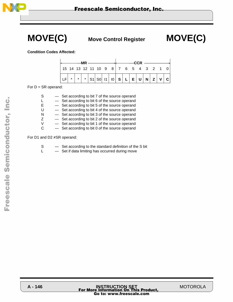
Fre
esc
ale
Se
mic
on
du
cto
r, I
Freescale Semiconductor, Inc.n
c..
.
Condition Codes Affected:
For D = SR operand:
S — Set according to bit 7 of the source operandL — Set according to bit 6 of the source operandE — Set according to bit 5 of the source operandU — Set according to bit 4 of the source operandN — Set according to bit 3 of the source operandZ — Set according to bit 2 of the source operandV — Set according to bit 1 of the source operandC — Set according to bit 0 of the source operand
For D1 and D2 ≠SR operand:
S — Set according to the standard definition of the S bitL — Set if data limiting has occurred during move
MOVE(C) Move Control Register MOVE(C)
15 14 13 12 11 10 9 8 7 6 5 4 3 2 1 0
LF * * * S1 S0 I1 I0 S L E U N Z V C
CCRMR
A - 146 INSTRUCTION SET MOTOROLA For More Information On This Product,
Go to: www.freescale.com
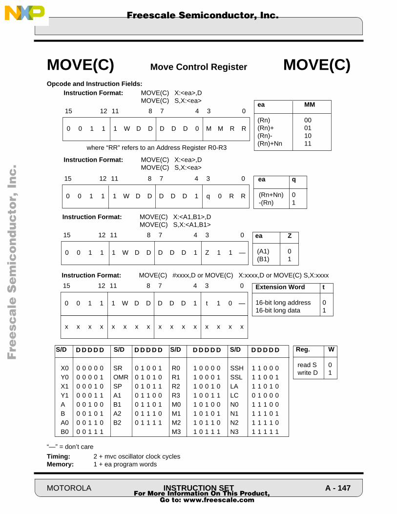
Fre
esc
ale
Se
mic
on
du
cto
r, I
Freescale Semiconductor, Inc.n
c..
.
Opcode and Instruction Fields:
“—” = don’t care
Timing: 2 + mvc oscillator clock cyclesMemory: 1 + ea program words
MOVE(C) Move Control Register MOVE(C)
0 0 1 1 1 W D D D D D 0 M M R R
15 12 11 8 7 4 3 0
0 0 1 1 1 W D D D D D 1 q 0 R R
15 12 11 8 7 4 3 0
Extension Word t
16-bit long address 016-bit long data 1
ea q
(Rn+Nn) 0-(Rn) 1
x x x x x x x x x x x x x x x x
0 0 1 1 1 W D D D D D 1 t 1 0 —
15 12 11 8 7 4 3 0
ea MM
(Rn) 00(Rn)+ 01(Rn)- 10(Rn)+Nn 11
D D D D D
X0 0 0 0 0 0Y0 0 0 0 0 1X1 0 0 0 1 0Y1 0 0 0 1 1A 0 0 1 0 0B 0 0 1 0 1A0 0 0 1 1 0B0 0 0 1 1 1
D D D D D
SR 0 1 0 0 1OMR 0 1 0 1 0SP 0 1 0 1 1A1 0 1 1 0 0B1 0 1 1 0 1A2 0 1 1 1 0B2 0 1 1 1 1
D D D D D
R0 1 0 0 0 0R1 1 0 0 0 1R2 1 0 0 1 0R3 1 0 0 1 1M0 1 0 1 0 0M1 1 0 1 0 1M2 1 0 1 1 0M3 1 0 1 1 1
D D D D D
SSH 1 1 0 0 0SSL 1 1 0 0 1LA 1 1 0 1 0LC 0 1 0 0 0N0 1 1 1 0 0N1 1 1 1 0 1N2 1 1 1 1 0N3 1 1 1 1 1
where “RR” refers to an Address Register R0-R3
Reg. W
read S 0 write D 1
0 0 1 1 1 W D D D D D 1 Z 1 1 —
15 12 11 8 7 4 3 0 ea Z
(A1) 0 (B1) 1
S/D S/D S/DS/D
Instruction Format: MOVE(C) X:<ea>,DMOVE(C) S,X:<ea>
Instruction Format: MOVE(C) X:<ea>,DMOVE(C) S,X:<ea>
Instruction Format: MOVE(C) X:<A1,B1>,DMOVE(C) S,X:<A1,B1>
Instruction Format: MOVE(C) #xxxx,D or MOVE(C) X:xxxx,D or MOVE(C) S,X:xxxx
MOTOROLA INSTRUCTION SET A - 147 For More Information On This Product,
Go to: www.freescale.com
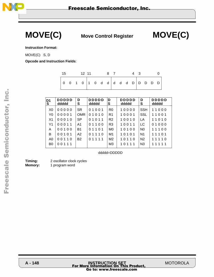
Fre
esc
ale
Se
mic
on
du
cto
r, I
Freescale Semiconductor, Inc.n
c..
.
Instruction Format:
MOVE(C) S, D
Opcode and Instruction Fields:
Timing: 2 oscillator clock cyclesMemory: 1 program word
MOVE(C) Move Control Register MOVE(C)
0 0 1 0 1 0 d d d d d D D D D D
15 12 11 8 7 4 3 0
D D D D D
X0 0 0 0 0 0Y0 0 0 0 0 1X1 0 0 0 1 0Y1 0 0 0 1 1A 0 0 1 0 0B 0 0 1 0 1A0 0 0 1 1 0B0 0 0 1 1 1
D D D D D
SR 0 1 0 0 1OMR 0 1 0 1 0SP 0 1 0 1 1A1 0 1 1 0 0B1 0 1 1 0 1A2 0 1 1 1 0B2 0 1 1 1 1
D D D D D
R0 1 0 0 0 0R1 1 0 0 0 1R2 1 0 0 1 0R3 1 0 0 1 1M0 1 0 1 0 0M1 1 0 1 0 1M2 1 0 1 1 0M3 1 0 1 1 1
D D D D D
SSH 1 1 0 0 0SSL 1 1 0 0 1LA 1 1 0 1 0LC 0 1 0 0 0N0 1 1 1 0 0N1 1 1 1 0 1N2 1 1 1 1 0N3 1 1 1 1 1
ddddd=DDDDD
D1 D D DS ddddd S ddddd S ddddd S ddddd
A - 148 INSTRUCTION SET MOTOROLA For More Information On This Product,
Go to: www.freescale.com

Fre
esc
ale
Se
mic
on
du
cto
r, I
Freescale Semiconductor, Inc.n
c..
.
Instruction Format:
MOVE(C) X:(R2+xx),DMOVE(C) S,X:(R2+xx)
Opcode and Instruction Fields:
“—” = don’t care
Timing: 2+mvc oscillator clock cyclesMemory: 2 program words
MOVE(C) Move Control Register MOVE(C)
D D D D D
X0 0 0 0 0 0Y0 0 0 0 0 1X1 0 0 0 1 0Y1 0 0 0 1 1A 0 0 1 0 0B 0 0 1 0 1A0 0 0 1 1 0B0 0 0 1 1 1
D D D D D
SR 0 1 0 0 1OMR 0 1 0 1 0SP 0 1 0 1 1A1 0 1 1 0 0B1 0 1 1 0 1A2 0 1 1 1 0B2 0 1 1 1 1
D D D D D
R0 1 0 0 0 0R1 1 0 0 0 1R2 1 0 0 1 0R3 1 0 0 1 1M0 1 0 1 0 0M1 1 0 1 0 1M2 1 0 1 1 0M3 1 0 1 1 1
D D D D D
SSH 1 1 0 0 0SSL 1 1 0 0 1LA 1 1 0 1 0LC 0 1 0 0 0N0 1 1 1 0 0N1 1 1 1 0 1N2 1 1 1 1 0N3 1 1 1 1 1
0 0 1 1 1 W D D D D D 0 — — — —
0 0 0 0 0 1 0 1 B B B B B B B B
15 12 11 8 7 4 3 0
Reg. W
read S1 0write D1 1
D D D DS ddddd S ddddd S ddddd S ddddd
“xx” refers to a 8-bit data BBBBBBBB
MOTOROLA INSTRUCTION SET A - 149 For More Information On This Product,
Go to: www.freescale.com

Fre
esc
ale
Se
mic
on
du
cto
r, I
Freescale Semiconductor, Inc.n
c..
.
Operation: Assembler Syntax:
#xx → D MOVE(I) #xx,D
Description: The 8-bit signed immediate operand is stored in the low byte of destination register D afterhaving been sign extended.
Example:
MOVE(I) #<$84,X1 ; equivalent to MOVE #<−$7C,X1
Explanation of Example:Prior to execution, X1 contains the value $FFFF. Execution of the instruction moves the value $FF84 into X1.
MOVE(I) Move Immediate Short MOVE(I)
Before Execution
FFFF
X1
After Execution
FF84
X1
A - 150 INSTRUCTION SET MOTOROLA For More Information On This Product,
Go to: www.freescale.com

Fre
esc
ale
Se
mic
on
du
cto
r, I
Freescale Semiconductor, Inc.n
c..
.
Condition Codes:The condition codes are not affected by this instruction.
Instruction Format:
MOVE(I) #xx,D
Opcode and Instruction Fields:
Timing: 2 oscillator clock cyclesMemory: 1 program word
MOVE(I) Move Immediate Short MOVE(I)
0 0 1 0 0 0 D D B B B B B B B B
15 12 11 8 7 4 3 0Destination DD
X0 00Y0 01X1 10Y1 11
“xx” refers to a 8-bit data BBBBBBBB
MOTOROLA INSTRUCTION SET A - 151 For More Information On This Product,
Go to: www.freescale.com
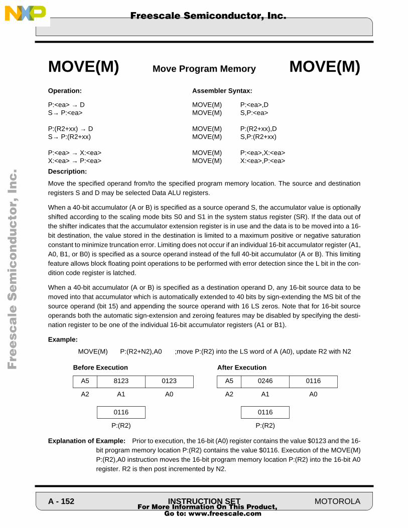
F
ree
sca
le S
em
ico
nd
uc
tor,
I
Freescale Semiconductor, Inc.n
c..
.
Operation: Assembler Syntax:
P:<ea> → D MOVE(M) P:<ea>,DS→ P:<ea> MOVE(M) S,P:<ea>
P:(R2+xx) → D MOVE(M) P:(R2+xx),DS→ P:(R2+xx) MOVE(M) S,P:(R2+xx)
P:<ea> → X:<ea> MOVE(M) P:<ea>,X:<ea>X:<ea> → P:<ea> MOVE(M) X:<ea>,P:<ea>
Description:
Move the specified operand from/to the specified program memory location. The source and destinationregisters S and D may be selected Data ALU registers.
When a 40-bit accumulator (A or B) is specified as a source operand S, the accumulator value is optionallyshifted according to the scaling mode bits S0 and S1 in the system status register (SR). If the data out ofthe shifter indicates that the accumulator extension register is in use and the data is to be moved into a 16-bit destination, the value stored in the destination is limited to a maximum positive or negative saturationconstant to minimize truncation error. Limiting does not occur if an individual 16-bit accumulator register (A1,A0, B1, or B0) is specified as a source operand instead of the full 40-bit accumulator (A or B). This limitingfeature allows block floating point operations to be performed with error detection since the L bit in the con-dition code register is latched.
When a 40-bit accumulator (A or B) is specified as a destination operand D, any 16-bit source data to bemoved into that accumulator which is automatically extended to 40 bits by sign-extending the MS bit of thesource operand (bit 15) and appending the source operand with 16 LS zeros. Note that for 16-bit sourceoperands both the automatic sign-extension and zeroing features may be disabled by specifying the desti-nation register to be one of the individual 16-bit accumulator registers (A1 or B1).
Example:
MOVE(M) P:(R2+N2),A0 ;move P:(R2) into the LS word of A (A0), update R2 with N2
Explanation of Example: Prior to execution, the 16-bit (A0) register contains the value $0123 and the 16-bit program memory location P:(R2) contains the value $0116. Execution of the MOVE(M)P:(R2),A0 instruction moves the 16-bit program memory location P:(R2) into the 16-bit A0register. R2 is then post incremented by N2.
MOVE(M) Move Program Memory MOVE(M)
0116
P:(R2)
0116
P:(R2)
After Execution
A5 0246 0116
A2 A1 A0
Before Execution
A5 8123 0123
A2 A1 A0
A - 152 INSTRUCTION SET MOTOROLA For More Information On This Product,
Go to: www.freescale.com
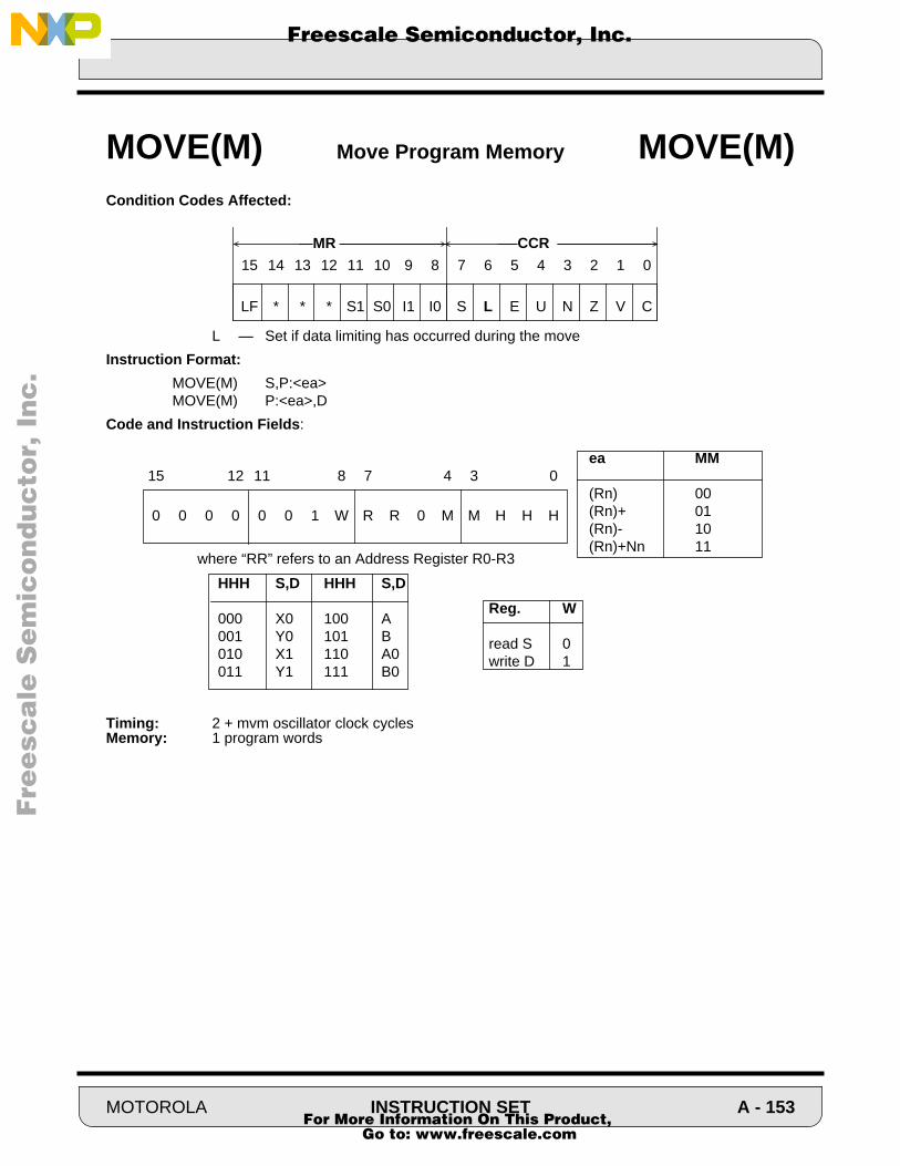
F
ree
sca
le S
em
ico
nd
uc
tor,
I
Freescale Semiconductor, Inc.n
c..
.
Condition Codes Affected:
L — Set if data limiting has occurred during the move
Instruction Format:
MOVE(M) S,P:<ea>MOVE(M) P:<ea>,D
Code and Instruction Fields:
Timing: 2 + mvm oscillator clock cyclesMemory: 1 program words
MOVE(M) Move Program Memory MOVE(M)
15 14 13 12 11 10 9 8 7 6 5 4 3 2 1 0
LF * * * S1 S0 I1 I0 S L E U N Z V C
CCRMR
0 0 0 0 0 0 1 W R R 0 M M H H H
15 12 11 8 7 4 3 0ea MM
(Rn) 00(Rn)+ 01(Rn)- 10(Rn)+Nn 11
where “RR” refers to an Address Register R0-R3
HHH S,D HHH S,D
000 X0 100 A001 Y0 101 B010 X1 110 A0011 Y1 111 B0
Reg. W
read S 0write D 1
MOTOROLA INSTRUCTION SET A - 153 For More Information On This Product,
Go to: www.freescale.com
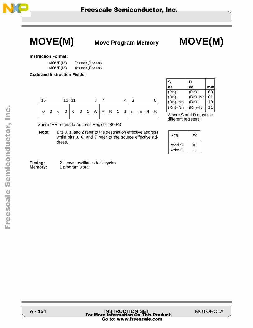
F
ree
sca
le S
em
ico
nd
uc
tor,
I
Freescale Semiconductor, Inc.n
c..
.
Instruction Format:
MOVE(M) P:<ea>,X:<ea>MOVE(M) X:<ea>,P:<ea>
Code and Instruction Fields:
Timing: 2 + mvm oscillator clock cyclesMemory: 1 program word
MOVE(M) Move Program Memory MOVE(M)
0 0 0 0 0 0 1 W R R 1 1 m m R R
15 12 11 8 7 4 3 0
where “RR” refers to Address Register R0-R3
Reg. W
read S 0write D 1
S Dea ea mm(Rn)+ (Rn)+ 00(Rn)+ (Rn)+Nn 01(Rn)+Nn (Rn)+ 10(Rn)+Nn (Rn)+Nn 11
Note: Bits 0, 1, and 2 refer to the destination effective addresswhile bits 3, 6, and 7 refer to the source effective ad-dress.
Where S and D must usedifferent registers.
A - 154 INSTRUCTION SET MOTOROLA For More Information On This Product,
Go to: www.freescale.com
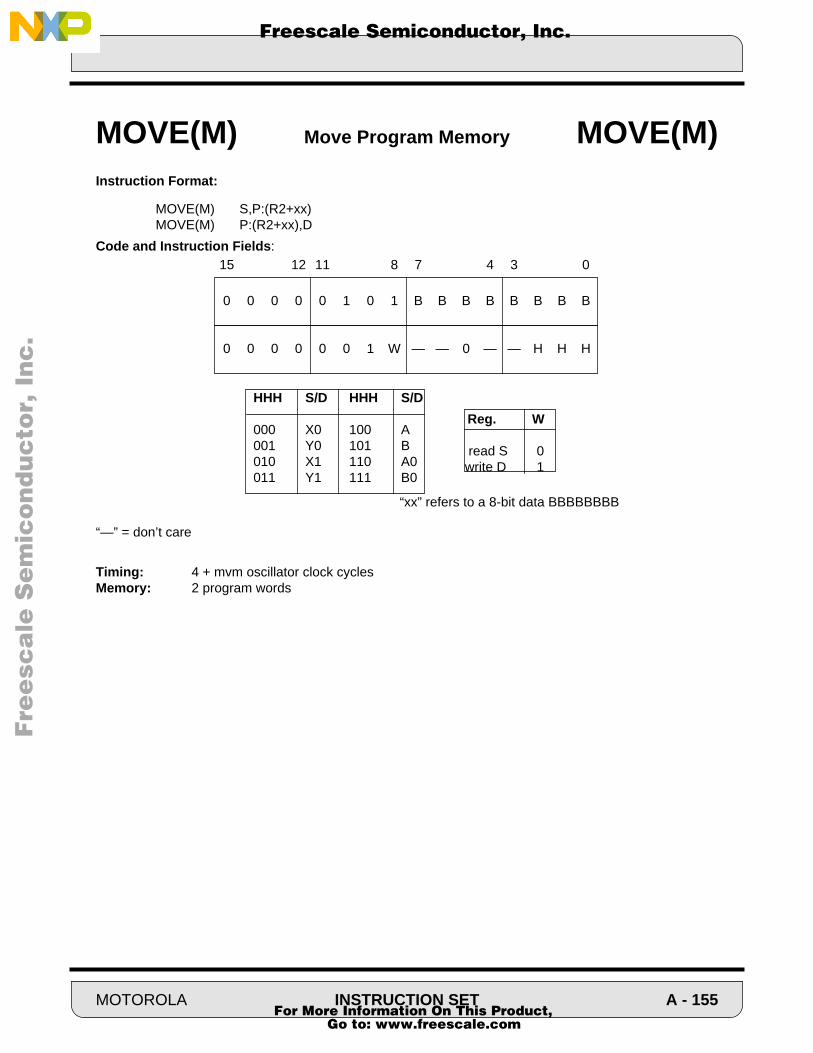
F
ree
sca
le S
em
ico
nd
uc
tor,
I
Freescale Semiconductor, Inc.n
c..
.
Instruction Format:
MOVE(M) S,P:(R2+xx)MOVE(M) P:(R2+xx),D
Code and Instruction Fields:
“—” = don’t care
Timing: 4 + mvm oscillator clock cyclesMemory: 2 program words
MOVE(M) Move Program Memory MOVE(M)
HHH S/D HHH S/D
000 X0 100 A001 Y0 101 B010 X1 110 A0011 Y1 111 B0
0 0 0 0 0 0 1 W — — 0 — — H H H
0 0 0 0 0 1 0 1 B B B B B B B B
15 12 11 8 7 4 3 0
Reg. W
read S 0write D 1
“xx” refers to a 8-bit data BBBBBBBB
MOTOROLA INSTRUCTION SET A - 155 For More Information On This Product,
Go to: www.freescale.com
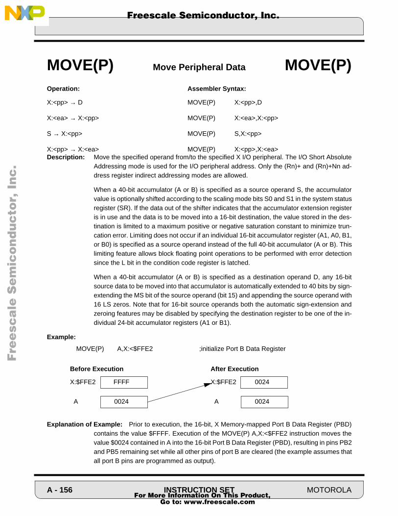
F
ree
sca
le S
em
ico
nd
uc
tor,
I
Freescale Semiconductor, Inc.n
c..
.
Operation: Assembler Syntax:
X:<pp> → D MOVE(P) X:<pp>,D
X:<ea> → X:<pp> MOVE(P) X:<ea>,X:<pp>
S → X:<pp> MOVE(P) S,X:<pp>
X:<pp> → X:<ea> MOVE(P) X:<pp>,X:<ea>Description: Move the specified operand from/to the specified X I/O peripheral. The I/O Short Absolute
Addressing mode is used for the I/O peripheral address. Only the (Rn)+ and (Rn)+Nn ad-dress register indirect addressing modes are allowed.
When a 40-bit accumulator (A or B) is specified as a source operand S, the accumulatorvalue is optionally shifted according to the scaling mode bits S0 and S1 in the system statusregister (SR). If the data out of the shifter indicates that the accumulator extension registeris in use and the data is to be moved into a 16-bit destination, the value stored in the des-tination is limited to a maximum positive or negative saturation constant to minimize trun-cation error. Limiting does not occur if an individual 16-bit accumulator register (A1, A0, B1,or B0) is specified as a source operand instead of the full 40-bit accumulator (A or B). Thislimiting feature allows block floating point operations to be performed with error detectionsince the L bit in the condition code register is latched.
When a 40-bit accumulator (A or B) is specified as a destination operand D, any 16-bitsource data to be moved into that accumulator is automatically extended to 40 bits by sign-extending the MS bit of the source operand (bit 15) and appending the source operand with16 LS zeros. Note that for 16-bit source operands both the automatic sign-extension andzeroing features may be disabled by specifying the destination register to be one of the in-dividual 24-bit accumulator registers (A1 or B1).
Example:
MOVE(P) A,X:<$FFE2 ;initialize Port B Data Register
Explanation of Example: Prior to execution, the 16-bit, X Memory-mapped Port B Data Register (PBD)contains the value $FFFF. Execution of the MOVE(P) A,X:<$FFE2 instruction moves thevalue $0024 contained in A into the 16-bit Port B Data Register (PBD), resulting in pins PB2and PB5 remaining set while all other pins of port B are cleared (the example assumes thatall port B pins are programmed as output).
MOVE(P) Move Peripheral Data MOVE(P)
Before Execution
X:$FFE2 FFFF
A 0024
After Execution
X:$FFE2 0024
A 0024
A - 156 INSTRUCTION SET MOTOROLA For More Information On This Product,
Go to: www.freescale.com

F
ree
sca
le S
em
ico
nd
uc
tor,
I
Freescale Semiconductor, Inc.n
c..
.
Condition Codes Affected:
S — Set according to the standard definition of the S bitL — Set if data limiting has occurred during move
Opcode and Instruction Fields:
Timing: 4 + mvp oscillator clock cyclesMemory: 1 program word
MOVE(P) Move Peripheral Data MOVE(P)
15 14 13 12 11 10 9 8 7 6 5 4 3 2 1 0
LF * * * S1 S0 I1 I0 S L E U N Z V C
CCRMR
Reg. W
read S 0write D 1
0 0 0 1 1 0 0 W H H 1 p p p p p
15 12 11 8 7 4 3 0
0 0 0 0 1 1 0 W R R m p p p p p
15 12 11 8 7 4 3 0
S,D HH
X0 00Y0 01A 10B 11
where “RR” refers to an Address Register R0-R3
ea m
(Rn)+ 0(Rn)+Nn 1
pp = 5-bit absolute address = ppppp
Instruction Format:
MOVE(P) X:<pp>,DMOVE(P) S,X:<pp>
Instruction Format:
MOVE(P) X:<ea>,X:<pp>MOVE(P) X:<pp>,X:<ea>
MOTOROLA INSTRUCTION SET A - 157 For More Information On This Product,
Go to: www.freescale.com

F
ree
sca
le S
em
ico
nd
uc
tor,
I
Freescale Semiconductor, Inc.n
c..
.
Operation: Assembler Syntax:
X:<aa> → D MOVE(S) X:<aa>,D
S → X:<aa> MOVE(S) S,X:<aa>
Description: Move the specified operand from/to the lower 32 memory locations in X Data memory. The5-bit Absolute short address is zero extended
When a 40-bit accumulator (A or B) is specified as a source operand S, the accumulatorvalue is optionally shifted according to the scaling mode bits S0 and S1 in the system statusregister (SR). If the data out of the shifter indicates that the accumulator extension registeris in use and the data is to be moved into a 16-bit destination, the value stored in the des-tination is limited to a maximum positive or negative saturation constant to minimize trun-cation error. Limiting does not occur if an individual 16-bit accumulator register (A1, A0, B1,or B0) is specified as a source operand instead of the full 40-bit accumulator (A or B). Thislimiting feature allows block floating point operations to be performed with error detectionsince the L bit in the condition code register is latched.
When a 40-bit accumulator (A or B) is specified as a destination operand D, any 16-bitsource data to be moved into that accumulator is automatically extended to 40 bits by sign-extending the MS bit of the source operand (bit 15) and appending the source operand with16 LS zeros. Note that for 16-bit source operands both the automatic sign-extension andzeroing features may be disabled by specifying the destination register to be one of the in-dividual 24-bit accumulator registers (A1 or B1).
Example:
MOVE(S) A,X:<$10 ;initialize X:$0
Explanation of Example: Prior to execution, X:$10 contains the value $FFFF. Execution of the instruc-tion moves the value $0024 into the memory location
MOVE(S) Move Absolute Short MOVE(S)
Before Execution After Execution
A
X:$0010 X:$0010
A0024
FFFF
0024
0024
A - 158 INSTRUCTION SET MOTOROLA For More Information On This Product,
Go to: www.freescale.com
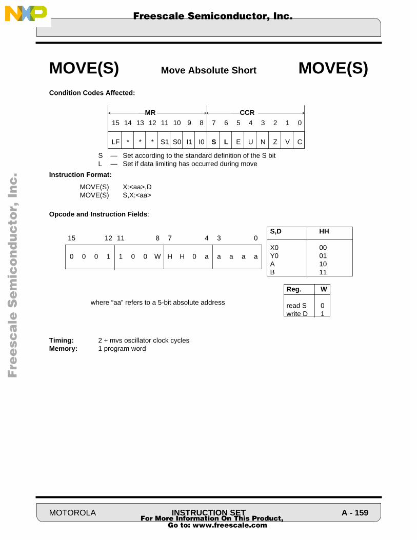
F
ree
sca
le S
em
ico
nd
uc
tor,
I
Freescale Semiconductor, Inc.n
c..
.
Condition Codes Affected:
S — Set according to the standard definition of the S bitL — Set if data limiting has occurred during move
Instruction Format:
MOVE(S) X:<aa>,DMOVE(S) S,X:<aa>
Opcode and Instruction Fields:
Timing: 2 + mvs oscillator clock cyclesMemory: 1 program word
MOVE(S) Move Absolute Short MOVE(S)
15 14 13 12 11 10 9 8 7 6 5 4 3 2 1 0
LF * * * S1 S0 I1 I0 S L E U N Z V C
CCRMR
0 0 0 1 1 0 0 W H H 0 a a a a a
15 12 11 8 7 4 3 0S,D HH
X0 00Y0 01A 10B 11
where “aa” refers to a 5-bit absolute address
Reg. W
read S 0write D 1
MOTOROLA INSTRUCTION SET A - 159 For More Information On This Product,
Go to: www.freescale.com
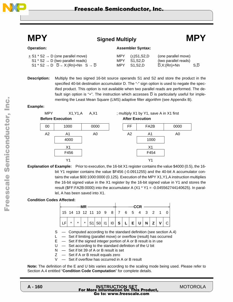
F
ree
sca
le S
em
ico
nd
uc
tor,
I
Freescale Semiconductor, Inc.n
c..
.
Operation: Assembler Syntax:
+ S1 * S2 → D (one parallel move) MPY (+)S1,S2,D (one parallel move) S1 * S2 → D (two parallel reads) MPY S1,S2,D (two parallel reads) S1 * S2 → D D→ X:(Rn)+Nn S → D MPY S1,S2,D D,X:(Rn)+Nn S,D
Description: Multiply the two signed 16-bit source operands S1 and S2 and store the product in thespecified 40-bit destination accumulator D. The “-” sign option is used to negate the spec-ified product. This option is not available when two parallel reads are performed. The de-fault sign option is “+”. The instruction which accesses D is particularly useful for imple-menting the Least Mean Square (LMS) adaptive filter algorithm (see Appendix B).
Example:
MPY X1,Y1,A A,X1 ; multiply X1 by Y1, save A in X1 first
Explanation of Example: Prior to execution, the 16-bit X1 register contains the value $4000 (0.5), the 16-bit Y1 register contains the value $F456 (-0.0911255) and the 40-bit A accumulator con-tains the value $00:1000:0000 (0.125). Execution of the MPY X1,Y1,A instruction multipliesthe 16-bit signed value in the X1 register by the 16-bit signed value in Y1 and stores theresult ($FF:FA2B:0000) into the accumulator A (X1 * Y1 = -0.045562744140625). In paral-lel, A has been saved into X1.
Condition Codes Affected:
S — Computed according to the standard definition (see section A.4)L — Set if limiting (parallel move) or overflow (result) has occurredE — Set if the signed integer portion of A or B result is in useU — Set according to the standard definition of the U bitN — Set if bit 39 of A or B result is setZ — Set if A or B result equals zeroV — Set if overflow has occurred in A or B result
Note: The definition of the E and U bits varies according to the scaling mode being used. Please refer toSection A.4 entitled “Condition Code Computation” for complete details.
MPY Signed Multiply MPY
4000
X1
After Execution
FF FA2B 0000
A2 A1 A0
Before Execution
00 1000 0000
A2 A1 A0
1000
X1 F456
Y1
F454
Y1
15 14 13 12 11 10 9 8 7 6 5 4 3 2 1 0
LF * * * S1 S0 I1 I0 S L E U N Z V C
CCRMR
A - 160 INSTRUCTION SET MOTOROLA For More Information On This Product,
Go to: www.freescale.com

F
ree
sca
le S
em
ico
nd
uc
tor,
I
Freescale Semiconductor, Inc.n
c..
.
Instruction Fields:
Timing: 2 + mv oscillator clock cyclesMemory: 1 program word
MPY Signed Multiply MPY
1 m R R H H H H 1 k 0 0 F Q Q Q
15 12 11 8 7 4 3 0
0 1 1 m m K K K 1 x x 0 F 0 Q Q
15 12 11 8 7 4 3 0
0 0 0 1 0 1 1 0 R R D D F Q Q Q
15 12 11 8 7 4 3 0
Sign k+ 0- 1
Instruction Format: MPY S1,S2,D D,X:(Rn)+Nn S,D (one memory write, Opcode: one data register move)
Instruction Format: MPY S1,S2,D (two parallel reads)Opcode:
Instruction Format: MPY (+)S2,S1,D (one parallel move)Opcode:
Instruction Fields: Please see the “X Memory Data Move” description in the parallel move section for details on the m, RR, HHH, and W data fields.
Instruction Fields: Please see the “X Memory Data Write and Register Data Move” description in the parallel move section for details on the RR and DD data fields.
Instruction Fields: Please see the “Dual X Memory Data Read” description in the parallel move sec-tion for details on the mm and KKK data fields.
One Or Two Parallel OperationS1,S2,D QQQ FY0,X0,A 1 0 0 0Y0,X0,B 1 0 0 1Y1,X0,A 1 0 1 0Y1,X0,B 1 0 1 1Y0,X1,A 1 1 0 0Y0,X1,B 1 1 0 1Y1,X1,A 1 1 1 0Y1,X1,B 1 1 1 1
S1,S2,D QQQ FX0,X0,A 0 0 0 0X0,X0,B 0 0 0 1X1,X0,A 0 0 1 0X1,X0,B 0 0 1 1A1,Y0,A 0 1 0 0A1,Y0,B 0 1 0 1B1,X0,A 0 1 1 0B1,X0,B 0 1 1 1
Two Parallel ReadsS1,S2,D QQ FX1,Y0,A 1 0 0X1,Y0,B 1 0 1X1,Y1,A 1 1 0X1,Y1,B 1 1 1
S1,S2,D QQ FX0,Y0,A 0 0 0X0,Y0,B 0 0 1X0,Y1,A 0 1 0X0,Y1,B 0 1 1
MOTOROLA INSTRUCTION SET A - 161 For More Information On This Product,
Go to: www.freescale.com
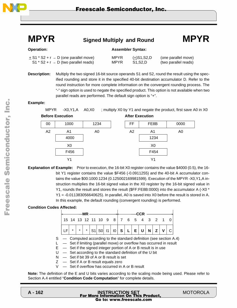
F
ree
sca
le S
em
ico
nd
uc
tor,
I
Freescale Semiconductor, Inc.n
c..
.
Operation: Assembler Syntax:
+ S1 * S2 + r → D (one parallel move) MPYR (+)S1,S2,D (one parallel move) S1 * S2 + r → D (two parallel reads) MPYR S1,S2,D (two parallel reads)
Description: Multiply the two signed 16-bit source operands S1 and S2, round the result using the spec-ified rounding and store it in the specified 40-bit destination accumulator D. Refer to theround instruction for more complete information on the convergent rounding process. The“-” sign option is used to negate the specified product. This option is not available when twoparallel reads are performed. The default sign option is “+”.
Example:
MPYR -X0,Y1,A A0,X0 ; multiply X0 by Y1 and negate the product, first save A0 in X0
Explanation of Example: Prior to execution, the 16-bit X0 register contains the value $4000 (0.5), the 16-bit Y1 register contains the value $F456 (-0.0911255) and the 40-bit A accumulator con-tains the value $00:1000:1234 (0.125002169981599). Execution of the MPYR -X0,Y1,A in-struction multiplies the 16-bit signed value in the X0 register by the 16-bit signed value inY1, rounds the result and stores the result ($FF:FE8B:0000) into the accumulator A (-X0 *Y1 = -0.011383056640625). In parallel, A0 is saved into X0 before the result is stored in A.In this example, the default rounding (convergent rounding) is performed.
Condition Codes Affected:
S — Computed according to the standard definition (see section A.4)L — Set if limiting (parallel move) or overflow has occurred in resultE — Set if the signed integer portion of A or B result is in useU — Set according to the standard definition of the U bitN — Set if bit 39 of A or B result is setZ — Set if A or B result equals zeroV — Set if overflow has occurred in A or B result
Note: The definition of the E and U bits varies according to the scaling mode being used. Please refer toSection A.4 entitled “Condition Code Computation” for complete details.
MPYR Signed Multiply and Round MPYR
4000
X0
After Execution
FF FE8B 0000
A2 A1 A0
Before Execution
00 1000 1234
A2 A1 A0
1234
X0
F456
Y1
F454
Y1
15 14 13 12 11 10 9 8 7 6 5 4 3 2 1 0
LF * * * S1 S0 I1 I0 S L E U N Z V C
CCRMR
A - 162 INSTRUCTION SET MOTOROLA For More Information On This Product,
Go to: www.freescale.com
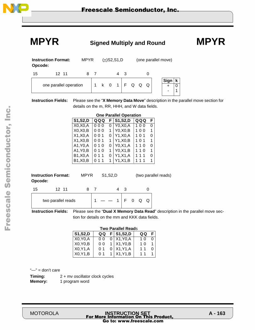
F
ree
sca
le S
em
ico
nd
uc
tor,
I
Freescale Semiconductor, Inc.n
c..
.
“—” = don’t care
Timing: 2 + mv oscillator clock cyclesMemory: 1 program word
MPYR Signed Multiply and Round MPYR
one parallel operation 1 k 0 1 F Q Q Q
15 12 11 8 7 4 3 0
two parallel reads 1 — — 1 F 0 Q Q
15 12 11 8 7 4 3 0
Sign k+ 0- 1
Instruction Fields: Please see the “Dual X Memory Data Read” description in the parallel move sec-tion for details on the mm and KKK data fields.
Instruction Format: MPYR S1,S2,D (two parallel reads)Opcode:
Instruction Fields: Please see the “X Memory Data Move” description in the parallel move section for details on the m, RR, HHH, and W data fields.
Instruction Format: MPYR (+)S2,S1,D (one parallel move)Opcode:
One Parallel OperationS1,S2,D QQQ FY0,X0,A 1 0 0 0Y0,X0,B 1 0 0 1Y1,X0,A 1 0 1 0Y1,X0,B 1 0 1 1Y0,X1,A 1 1 0 0Y0,X1,B 1 1 0 1Y1,X1,A 1 1 1 0Y1,X1,B 1 1 1 1
S1,S2,D QQQ FX0,X0,A 0 0 0 0X0,X0,B 0 0 0 1X1,X0,A 0 0 1 0X1,X0,B 0 0 1 1A1,Y0,A 0 1 0 0A1,Y0,B 0 1 0 1B1,X0,A 0 1 1 0B1,X0,B 0 1 1 1
Two Parallel ReadsS1,S2,D QQ FX1,Y0,A 1 0 0X1,Y0,B 1 0 1X1,Y1,A 1 1 0X1,Y1,B 1 1 1
S1,S2,D QQ FX0,Y0,A 0 0 0X0,Y0,B 0 0 1X0,Y1,A 0 1 0X0,Y1,B 0 1 1
MOTOROLA INSTRUCTION SET A - 163 For More Information On This Product,
Go to: www.freescale.com

F
ree
sca
le S
em
ico
nd
uc
tor,
I
Freescale Semiconductor, Inc.n
c..
.
Operation: Assembler Syntax:
S1 * S2 → D (S1 unsigned, S2 unsigned) MPYuu S1,S2,D (no parallel move)S1 * S2 → D (S1 signed, S2 unsigned) MPYsu S1,S2,D (no parallel move)
Description: Multiply the two 16-bit source operands S1 and S2 and store the product to the specified40-bit destination accumulator D. One or two of the source operands can be unsigned. Thismixed arithmetic multiply does not allow a parallel move and can be used for multiple pre-cision multiplications.
Example:
MPYuu X1,Y1,AMPYsu X1,Y1,A
Explanation of Example: The 16-bit X1 register contains the value $FFFF and the 16-bit Y1 registercontains the value $0062.
Execution of the MPYuu X1,Y1,A instruction multiplies the 16-bit unsigned value in the X1register by the 16-bit unsigned value in Y1 and stores the unsigned result into the accumu-lator A.
Execution of the MPYsu X1,Y1,A instruction multiplies the 16-bit signed value in the X1 reg-ister by the 16-bit unsigned value in Y1and stores the signed result into the accumulator A.
Warning: The saturation mode is always disabled during execution of MPY(su,uu), even when thesaturation bit (SA) of the OMR is set. Refer to Section 5.8.3 for more details.
MPY(su,uu) Mixed Multiply MPY(su,uu)
After MPYuu Execution
00 00C3 FFC3
A2 A1 A0
Before MPYuu Execution
00 1000 0000
A2 A1 A0
After MPYsu Execution
FF FFFF FFC3
A2 A1 A0
Before MPYsu Execution
00 00C3 FFC3
A2 A1 A0
X1
Before Execution After Execution
Y1 Y1
X1FFFF
0062
FFFF
0062
A - 164 INSTRUCTION SET MOTOROLA For More Information On This Product,
Go to: www.freescale.com

F
ree
sca
le S
em
ico
nd
uc
tor,
I
Freescale Semiconductor, Inc.n
c..
.
Condition Codes Affected:
E — Set if the signed integer portion of A or B result is in useU — Set according to the standard definition of the U bitN — Set if bit 39 of A or B result is setZ — Set if A or B result equals zeroV — Set if overflow has occurred in A or B result
Note: The definition of the E and U bits varies according to the scaling mode being used. Please refer to Section A.4 entitled “Condition Code Computation” for complete details.
Instruction Format:
MPY(uu) S1,S2,DMPY(su) S1,S2,D
Opcode:
Instruction Fields:
Timing: 2 oscillator clock cyclesMemory: 1 program word
MPY(su,uu) Mixed Multiply MPY(su,uu)
15 14 13 12 11 10 9 8 7 6 5 4 3 2 1 0
LF * * * S1 S0 I1 I0 S L E U N Z V C
CCRMR
0 0 0 1 0 1 0 1 1 1 0 0 F s Q Q
15 12 11 8 7 4 3 0
S1,S2,D QQ FX1,Y0,A 1 0 0X1,Y0,B 1 0 1X1,Y1,A 1 1 0X1,Y1,B 1 1 1
S1,S2,D QQ FY0,X0,A 0 0 0Y0,X0,B 0 0 1Y1,X0,A 0 1 0Y1,X0,B 0 1 1
Arithmetic s
su 0 uu 1
Note: For MPYsu, the order of S1, S2 is sig-nificant; the signed value will be taken fromS1 and the unsigned value will be taken fromS2 (i.e., MPYSU Y1, X0, A is legal whereasMPYSU X0, Y1, A is illegal).
MOTOROLA INSTRUCTION SET A - 165 For More Information On This Product,
Go to: www.freescale.com

F
ree
sca
le S
em
ico
nd
uc
tor,
I
Freescale Semiconductor, Inc.n
c..
.
Operation: Assembler Syntax:
0 - D → D (parallel move) NEG D (parallel move)
Description: The destination operand D is substracted from zero and the result is stored in the destina-tion accumulator.
Example:
NEG B X1,X:(R3)+ ;0-B → B, save X1, update R3
Explanation of Example: Prior to execution, the 40-bit B accumulator contains the value $00:1234:5678.The NEG B instruction takes the two’s complement of the value in the B accumulator andstores the 40-bit result back in the B accumulator.
Condition Codes Affected:
S — Computed according to the standard definition (see section A.4)C — Set if a borrow is generated from the MSB of the result.L — Set if limiting (parallel move) or overflow has occurred in resultE — Set if the signed integer portion of A or B is in useU — Set according to the standard definition of the U bitN — Set if bit 39 of A or B result is setZ — Set if A or B result equals zeroV — Set if overflow has occurred in A or B result
Note: The definition of the E and U bits varies according to the scaling mode being used. Please refer toSection A.4 entitled “Condition Code Computation” for complete details.
NEG Negate Accumulator NEG
A After Execution
FF EDCB A988
A2 A1 A0
A Before Execution
00 1234 5678
A2 A1 A0
0300
SR=MR:CCR
0309
SR=MR:CCR
15 14 13 12 11 10 9 8 7 6 5 4 3 2 1 0
LF * * * S1 S0 I1 I0 S L E U N Z V C
CCRMR
A - 166 INSTRUCTION SET MOTOROLA For More Information On This Product,
Go to: www.freescale.com
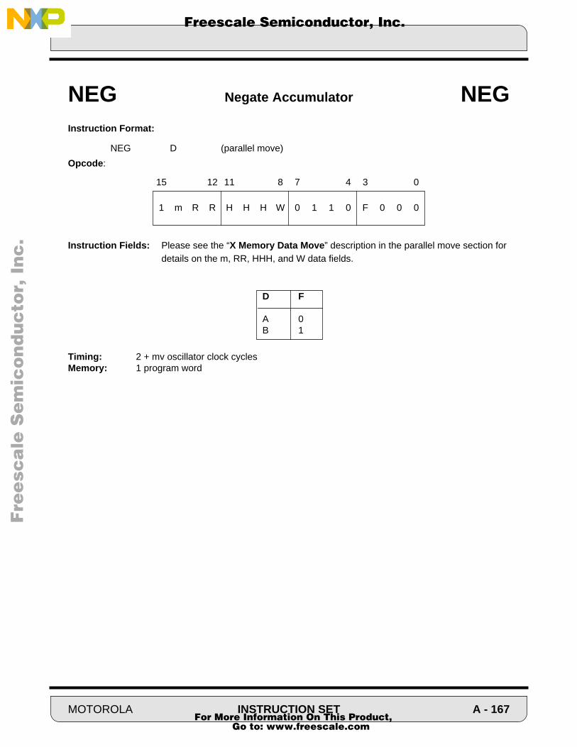
F
ree
sca
le S
em
ico
nd
uc
tor,
I
Freescale Semiconductor, Inc.n
c..
.
Instruction Format:
NEG D (parallel move)
Opcode:
Instruction Fields: Please see the “X Memory Data Move” description in the parallel move section for details on the m, RR, HHH, and W data fields.
Timing: 2 + mv oscillator clock cyclesMemory: 1 program word
NEG Negate Accumulator NEG
1 m R R H H H W 0 1 1 0 F 0 0 0
15 12 11 8 7 4 3 0
D F
A 0B 1
MOTOROLA INSTRUCTION SET A - 167 For More Information On This Product,
Go to: www.freescale.com
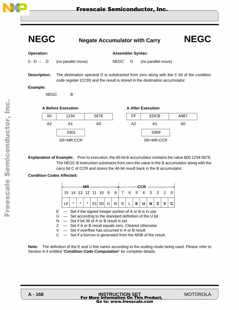
F
ree
sca
le S
em
ico
nd
uc
tor,
I
Freescale Semiconductor, Inc.n
c..
.
Operation: Assembler Syntax:
0 - D → D (no parallel move) NEGC D (no parallel move)
Description: The destination operand D is substracted from zero along with the C bit of the conditioncode register (CCR) and the result is stored in the destination accumulator.
Example:
NEGC B
Explanation of Example: Prior to execution, the 40-bit B accumulator contains the value $00:1234:5678.The NEGC B instruction substracts from zero the value in the B accumulator along with thecarry bit C of CCR and stores the 40-bit result back in the B accumulator.
Condition Codes Affected:
E — Set if the signed integer portion of A or B is in useU — Set according to the standard definition of the U bitN — Set if bit 39 of A or B result is setZ — Set if A or B result equals zero. Cleared otherwiseV — Set if overflow has occurred in A or B resultC — Set if a borrow is generated from the MSB of the result.
Note: The definition of the E and U bits varies according to the scaling mode being used. Please refer toSection A.4 entitled “Condition Code Computation” for complete details.
NEGC Negate Accumulator with Carry NEGC
A After Execution
FF EDCB A987
A2 A1 A0
A Before Execution
00 1234 5678
A2 A1 A0
0301
SR=MR:CCR
0309
SR=MR:CCR
15 14 13 12 11 10 9 8 7 6 5 4 3 2 1 0
LF * * * S1 S0 I1 I0 S L E U N Z V C
CCRMR
A - 168 INSTRUCTION SET MOTOROLA For More Information On This Product,
Go to: www.freescale.com

F
ree
sca
le S
em
ico
nd
uc
tor,
I
Freescale Semiconductor, Inc.n
c..
.
Instruction Format:
NEGC D
Opcode:
Instruction Fields:
Timing: 2 + mv oscillator clock cyclesMemory: 1 program word
NEGC Negate Accumulator with Carry NEGC
0 0 0 1 0 1 0 1 0 1 1 0 F 0 0 0
15 12 11 8 7 4 3 0
D F
A 0B 1
MOTOROLA INSTRUCTION SET A - 169 For More Information On This Product,
Go to: www.freescale.com

F
ree
sca
le S
em
ico
nd
uc
tor,
I
Freescale Semiconductor, Inc.n
c..
.
Operation: Assembler Syntax:
PC+1 → PC NOP
Description: Increment the program counter (PC). Pending pipeline actions, if any, are completed. Ex-ecution continues with the instruction following the NOP.
Example:
NOP increment the program counter
Explanation of Example:The NOP instruction increments the program counter (PC) and completes any pendingpipeline actions.
Condition Codes Affected:The condition codes are not affected by this instruction.
NOP No Operation NOP
A - 170 INSTRUCTION SET MOTOROLA For More Information On This Product,
Go to: www.freescale.com

F
ree
sca
le S
em
ico
nd
uc
tor,
I
Freescale Semiconductor, Inc.n
c..
.
Instruction Format:
NOP
Opcode:
Instruction Fields: none
Timing: 2 oscillator clock cyclesMemory: 1 program word
NOP No Operation NOP
0 0 0 0 0 0 0 0 0 0 0 0 0 0 0 0
15 12 11 8 7 4 3 0
MOTOROLA INSTRUCTION SET A - 171 For More Information On This Product,
Go to: www.freescale.com

Fre
esc
ale
Se
mic
on
du
cto
r, I
Freescale Semiconductor, Inc.n
c..
.
Operation: Assembler Syntax:
If E • U • Z = 1, then ASL D and Rn - 1 → Rn NORM Rn,Delse if E = 1, then ASR D and Rn + 1→ Rnelse NOP
where E denotes the logical complement of E, andwhere • denotes the logical AND operator
Description: Perform one normalization iteration on the specified destination operand D, update thespecified address register Rn based upon the results of that iteration, and store the resultback in the destination accumulator. This is a 40-bit operation. If the accumulator extensionis not in use and the accumulator is unnormalized and the accumulator is not zero, the des-tination operand is arithmetically shifted one bit to the left and the specified address registeris decremented by one. If the accumulator extension register is in use, the destination op-erand is arithmetically shifted one bit to the right and the specified address register is incre-mented by one. If the accumulator is normalized or zero, a NOP is executed and the spec-ified address register is not affected. Since the operation of the NORM instruction dependson the E, U, and Z condition code register bits, these bits must correctly reflect the currentstate of the destination accumulator prior to executing the NORM instruction. Note that theL and V bits in the condition code register will be cleared unless they have been improperlyset up prior to executing the NORM instruction.
Example:
REP #$1F ;maximum number of iterations (31) neededNORM R3,A ;perform 1 normalization iteration
Explanation of Example: Prior to execution, the 40-bit A accumulator contains the value $00:0000:0001and the 16-bit R3 address register contains the value $0000. The repetition of the NORMR3,A instruction normalizes the value in the 40-bit accumulator and stores the resultingnumber of shifts performed during that normalization process in the R3 address register. Anegative value reflects the number of left shifts performed while a positive value reflects thenumber of right shifts performed during the normalization process. In this example, thirtyleft shifts are required for normalization.
NORM Normalize Accumulator Iteration NORM
0000
R3
FFE2
R3
After Execution
00 4000 0000
A2 A1 A0
Before Execution
00 0000 0001
A2 A1 A0
A - 172 INSTRUCTION SET MOTOROLA For More Information On This Product,
Go to: www.freescale.com

Fre
esc
ale
Se
mic
on
du
cto
r, I
Freescale Semiconductor, Inc.n
c..
.
Condition Codes Affected:
S — Computed according to the standard definition (see section A.4)L — Set if overflow has occurred in A or B resultE — Set if the signed integer portion of A or B result is in useU — Set according to the standard definition of the U bitN — Set if bit 39 of A or B result is setZ — Set if A or B result equals zeroV — Set if bit 39 is changed as a result of a left shift
Note: The definition of the E and U bits varies according to the scaling mode being used. Please refer toSection A.4 entitled “Condition Code Computation” for complete details.
Instruction Format:
NORM Rn,D
Opcode:
Instruction Fields:
Timing: 2 oscillator clock cyclesMemory: 1 program word
NORM Normalize Accumulator Iteration NORM
15 14 13 12 11 10 9 8 7 6 5 4 3 2 1 0
LF * * * S1 S0 I1 I0 S L E U N Z V C
CCRMR
0 0 0 1 0 1 0 1 0 0 1 0 F 0 R R
15 12 11 8 7 4 3 0
D F
A 0B 1
Rn RR
R0 00R1 01R2 10R3 11
MOTOROLA INSTRUCTION SET A - 173 For More Information On This Product,
Go to: www.freescale.com
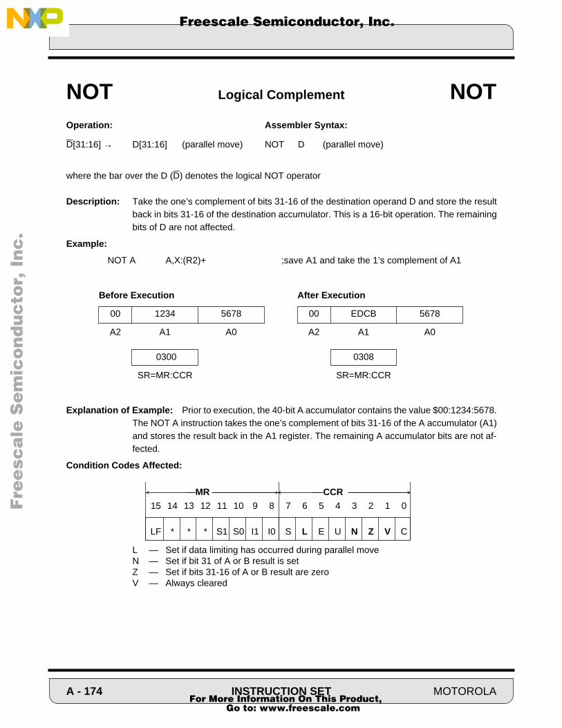
Fre
esc
ale
Se
mic
on
du
cto
r, I
Freescale Semiconductor, Inc.n
c..
.
Operation: Assembler Syntax:
D[31:16] → D[31:16] (parallel move) NOT D (parallel move)
where the bar over the D (D) denotes the logical NOT operator
Description: Take the one’s complement of bits 31-16 of the destination operand D and store the resultback in bits 31-16 of the destination accumulator. This is a 16-bit operation. The remainingbits of D are not affected.
Example:
NOT A A,X:(R2)+ ;save A1 and take the 1’s complement of A1
Explanation of Example: Prior to execution, the 40-bit A accumulator contains the value $00:1234:5678.The NOT A instruction takes the one’s complement of bits 31-16 of the A accumulator (A1)and stores the result back in the A1 register. The remaining A accumulator bits are not af-fected.
Condition Codes Affected:
L — Set if data limiting has occurred during parallel moveN — Set if bit 31 of A or B result is setZ — Set if bits 31-16 of A or B result are zeroV — Always cleared
NOT Logical Complement NOT
0300
SR=MR:CCR
0308
SR=MR:CCR
After Execution
00 EDCB 5678
A2 A1 A0
Before Execution
00 1234 5678
A2 A1 A0
15 14 13 12 11 10 9 8 7 6 5 4 3 2 1 0
LF * * * S1 S0 I1 I0 S L E U N Z V C
CCRMR
A - 174 INSTRUCTION SET MOTOROLA For More Information On This Product,
Go to: www.freescale.com

Fre
esc
ale
Se
mic
on
du
cto
r, I
Freescale Semiconductor, Inc.n
c..
.
Instruction Format:
NOT D (parallel move)
Opcode:
Instruction Fields: Please see the “X Memory Data Move” description in the parallel move section for details on the m, RR, HHH, and W data fields.
Timing: 2 + mv oscillator clock cyclesMemory: 1 program word
NOT Logical Complement NOT
1 m R R H H H W 0 1 1 0 F 0 0 1
15 12 11 8 7 4 3 0
D F
A 0B 1
MOTOROLA INSTRUCTION SET A - 175 For More Information On This Product,
Go to: www.freescale.com

Fre
esc
ale
Se
mic
on
du
cto
r, I
Freescale Semiconductor, Inc.n
c..
.
Operation: Assembler Syntax:
S + D[31:16] → D[31:16] (parallel move) OR S,D (parallel move)
where + denotes the logical inclusive OR operator
Description: Logically inclusive OR the source operand S with bits 31:16 of the destination operand Dand store the result in bits 31-16 of the destination accumulator. This instruction is a 16-bitoperation. The remaining bits of the destination operand D are not affected.
Example:
OR Y1,B B,X:(A1) ;save B1, OR Y1 with B:
Explanation of Example: Prior to execution, the 16-bit Y1 register contains the value $FF00 and the 40-bit B accumulator contains the value $00:1234:5678. The OR Y1,B instruction logicallyOR’s the 16-bit value in the Y1 register with bits 31:16 of the B accumulator (B1) and storesthe 40-bit result in the B accumulator.
Condition Codes Affected:
S — Computed according to the standard definition (see section A.4)L — Set if data limiting has occurred during parallel moveN — Set if bit 31 of A or B result is setZ — Set if bits 31-16 of A or B result are zeroV — Always cleared
OR Logical Inclusive OR OR
After Execution
00 FF34 5678
B2 B1 B0
Before Execution
00 1234 5678
B2 B1 B0
FF00
Y1
FF00
Y1
15 14 13 12 11 10 9 8 7 6 5 4 3 2 1 0
LF * * * S1 S0 I1 I0 S L E U N Z V C
CCRMR
A - 176 INSTRUCTION SET MOTOROLA For More Information On This Product,
Go to: www.freescale.com
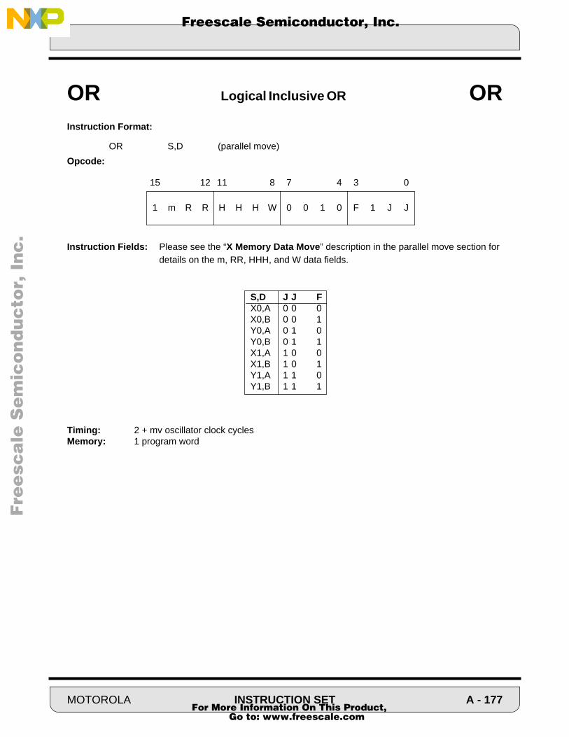
Fre
esc
ale
Se
mic
on
du
cto
r, I
Freescale Semiconductor, Inc.n
c..
.
Instruction Format:
OR S,D (parallel move)
Opcode:
Instruction Fields: Please see the “X Memory Data Move” description in the parallel move section for details on the m, RR, HHH, and W data fields.
Timing: 2 + mv oscillator clock cyclesMemory: 1 program word
OR Logical Inclusive OR OR
1 m R R H H H W 0 0 1 0 F 1 J J
15 12 11 8 7 4 3 0
S,D J J FX0,A 0 0 0X0,B 0 0 1Y0,A 0 1 0Y0,B 0 1 1X1,A 1 0 0X1,B 1 0 1Y1,A 1 1 0Y1,B 1 1 1
MOTOROLA INSTRUCTION SET A - 177 For More Information On This Product,
Go to: www.freescale.com
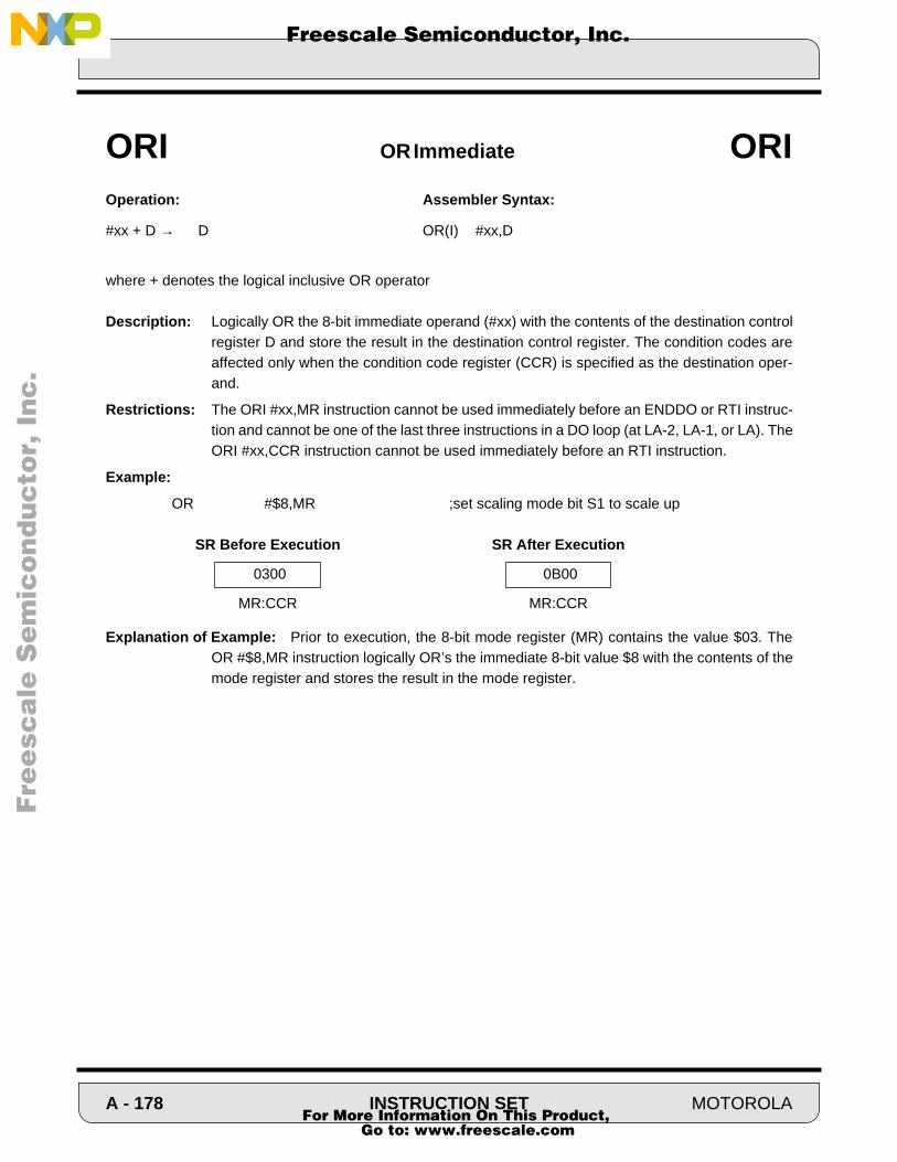
Fre
esc
ale
Se
mic
on
du
cto
r, I
Freescale Semiconductor, Inc.n
c..
.
Operation: Assembler Syntax:
#xx + D → D OR(I) #xx,D
where + denotes the logical inclusive OR operator
Description: Logically OR the 8-bit immediate operand (#xx) with the contents of the destination controlregister D and store the result in the destination control register. The condition codes areaffected only when the condition code register (CCR) is specified as the destination oper-and.
Restrictions: The ORI #xx,MR instruction cannot be used immediately before an ENDDO or RTI instruc-tion and cannot be one of the last three instructions in a DO loop (at LA-2, LA-1, or LA). TheORI #xx,CCR instruction cannot be used immediately before an RTI instruction.
Example:
OR #$8,MR ;set scaling mode bit S1 to scale up
Explanation of Example: Prior to execution, the 8-bit mode register (MR) contains the value $03. TheOR #$8,MR instruction logically OR’s the immediate 8-bit value $8 with the contents of themode register and stores the result in the mode register.
ORI OR Immediate ORI
SR Before Execution
0300
MR:CCR
SR After Execution
0B00
MR:CCR
A - 178 INSTRUCTION SET MOTOROLA For More Information On This Product,
Go to: www.freescale.com

Fre
esc
ale
Se
mic
on
du
cto
r, I
Freescale Semiconductor, Inc.n
c..
.
Condition Codes Affected:
For CCR operand:
S — Set if bit 7 of the immediate operand is setL — Set if bit 6 of the immediate operand is setE — Set if bit 5 of the immediate operand is setU — Set if bit 4 of the immediate operand is setN — Set if bit 3 of the immediate operand is setZ — Set if bit 2 of the immediate operand is setV — Set if bit 1 of the immediate operand is setC — Set if bit 0 of the immediate operand is set
For MR and OMR operands:
The condition codes are not affected using these operands
Instruction Format:
OR(I) #xx,D
Opcode:
Instruction Fields:: #xx = 8-bit Immediate Short Data — i i i i i i i i
Timing: 2 oscillator clock cyclesMemory: 1 program word
ORI OR Immediate ORI
15 14 13 12 11 10 9 8 7 6 5 4 3 2 1 0
LF * * * S1 S0 I1 I0 S L E U N Z V C
CCRMR
0 0 0 1 1 E E 1 i i i i i i i i
15 12 11 8 7 4 3 0
D E EMR 0 1CCR 1 1OMR 1 0
MOTOROLA INSTRUCTION SET A - 179 For More Information On This Product,
Go to: www.freescale.com

F
ree
sca
le S
em
ico
nd
uc
tor,
I
Freescale Semiconductor, Inc.n
c..
.
Operation: Assembler Syntax:
LC→ TEMP; X:(Rn) → LC REP X:(Rn)Repeat next instruction until LC = 1TEMP → LC
LC → TEMP; #xx → LC REP #xxRepeat next instruction until LC = 1TEMP → LC
LC → TEMP; S, → LC REP SRepeat next instruction until LC = 1TEMP → LC
Description: Repeat the single word instruction immediately following the REP instruction the specifiednumber of times. The value specifying the number of times the given instruction is to berepeated is loaded into the 16-bit loop counter (LC) register. The single word instruction isthen executed the specified number of times, decrementing the loop counter (LC) aftereach execution until (LC) = 1. When the REP instruction is in effect, the repeated instructionis fetched only one time and it remains in the instruction register for the duration of the loopcount. Thus, the REP instruction is not interruptible. The current loop counter (LC) value isstored in an internal temporary register. If LC is set equal to zero, the instruction is not re-peated. The instruction’s effective address specifies the address of the value which is to beloaded into the loop counter (LC).
If the A or B accumulator is specified as a source operand, the accumulator value is option-ally shifted according to the scaling mode bits S0 and S1 in the system status register (SR).If the data out of the shifter indicates that the accumulator extension is in use, the value tobe loaded into the loop counter (LC) register will be limited to a 16-bit maximum positive ornegative saturation constant to minimize the error due to truncation. The resulting valuesare then stored in the 16-bit loop counter (LC) register.
If the system stack register SSH is specified as a source operand, the system stack pointer(SP) is postdecremented by 1 after SSH has been read.
Restrictions:
The REP instruction can repeat any single word instruction except the REP instruction itself and any instruc-tion that changes program flow. The following instructions are not allowed to follow a REP instruction:
Immediately after REP DO, BRKcc Bcc, Jcc DEBUG, DEBUGccJCLR BRA, JMP WAITBScc, JScc BSR, JSRREP, REPcc RTIRTS STOPSWI Tcc
Also, a REP instruction cannot be the last instruction in a DO loop (at LA). The assembler will generate an error if any of the above instructions are found immediately following a REP instruction.
REP Repeat Next Instruction REP
A - 180 INSTRUCTION SET MOTOROLA For More Information On This Product,
Go to: www.freescale.com

F
ree
sca
le S
em
ico
nd
uc
tor,
I
Freescale Semiconductor, Inc.n
c..
.
Example:
:REP X0 ;repeat (X0) timesMAC X1,Y1,A X:(R1)+,X1 X:(R3)+,Y1 ;X1 * Y1 + A, w A, update X1,Y1
:
Explanation of Example: Prior to execution, the 16-bit X0 register contains the value $0100 and the 16-bit loop counter (LC) register contains the value $0000. Execution of the REP X0 instruction takes the 16-bit value in the X0 register and stores it in the 16-bit loop counter (LC) register. Thus, the single word MAC instruction immediately following the REP instruction is repeated $100 times.
Condition Codes Affected:
L — Set if data limiting occurred using A or B as source operands
REP Repeat Next Instruction REP
0100
X0
0100
X0
After Execution
0100
LC
Before Execution
0000
LC
15 14 13 12 11 10 9 8 7 6 5 4 3 2 1 0
LF * * * S1 S0 I1 I0 S L E U N Z V C
CCRMR
MOTOROLA INSTRUCTION SET A - 181 For More Information On This Product,
Go to: www.freescale.com

F
ree
sca
le S
em
ico
nd
uc
tor,
I
Freescale Semiconductor, Inc.n
c..
.
Instruction Format and Opcode:
REP X:(Rn)
“—” = don’t care
REP #xx
REP Repeat Next Instruction REP
0 0 0 0 0 0 0 0 1 1 1 — — — R R
15 12 11 8 7 4 3 0 Rn RR
R0 00R1 01R2 10R3 11
0 0 0 0 1 1 1 1 i i i i i i i i
15 12 11 8 7 4 3 0#xx: immediate 8-bit
short data = iiiiiiii
A - 182 INSTRUCTION SET MOTOROLA For More Information On This Product,
Go to: www.freescale.com
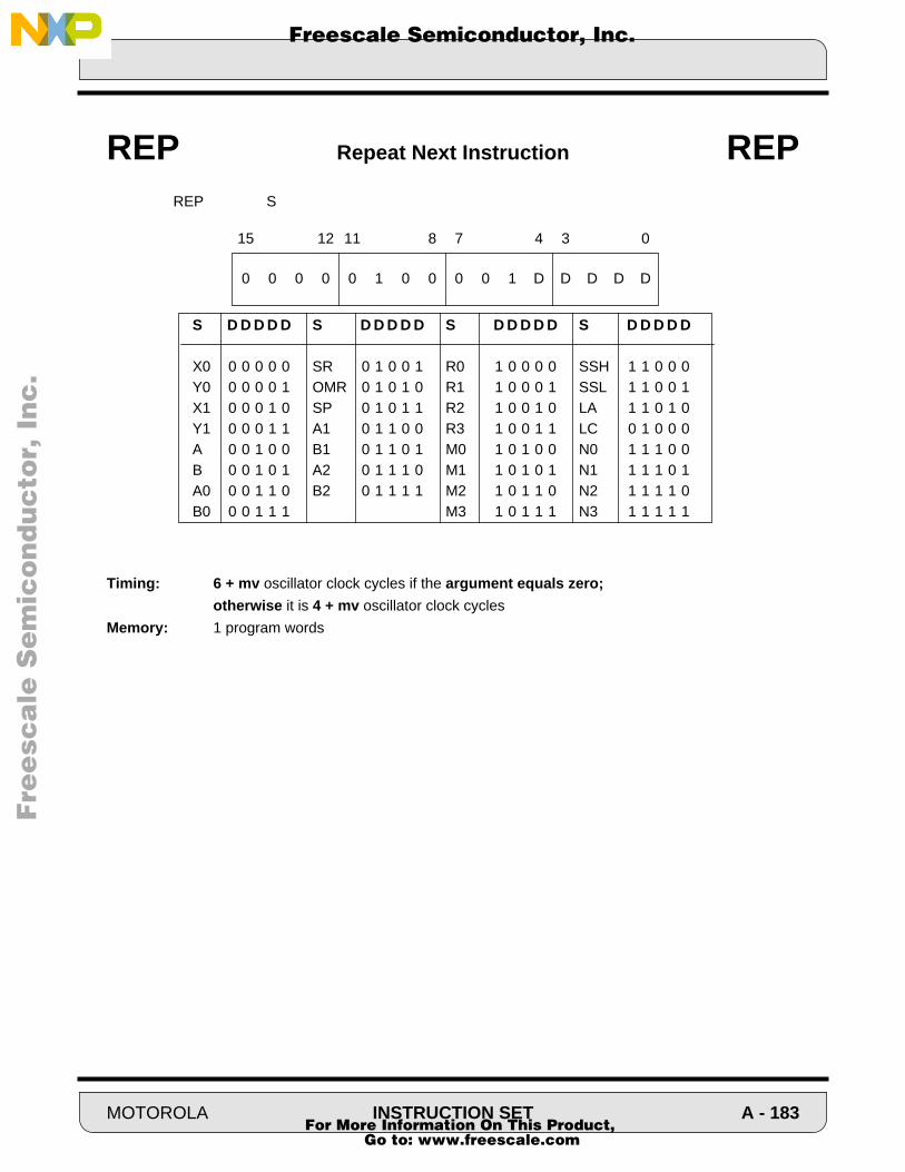
F
ree
sca
le S
em
ico
nd
uc
tor,
I
Freescale Semiconductor, Inc.n
c..
.
REP S
Timing: 6 + mv oscillator clock cycles if the argument equals zero;
otherwise it is 4 + mv oscillator clock cycles
Memory: 1 program words
REP Repeat Next Instruction REP
0 0 0 0 0 1 0 0 0 0 1 D D D D D
15 12 11 8 7 4 3 0
S D D D D D
X0 0 0 0 0 0Y0 0 0 0 0 1X1 0 0 0 1 0Y1 0 0 0 1 1A 0 0 1 0 0B 0 0 1 0 1A0 0 0 1 1 0B0 0 0 1 1 1
S D D D D D
SR 0 1 0 0 1OMR 0 1 0 1 0SP 0 1 0 1 1A1 0 1 1 0 0B1 0 1 1 0 1A2 0 1 1 1 0B2 0 1 1 1 1
S D D D D D
R0 1 0 0 0 0R1 1 0 0 0 1R2 1 0 0 1 0R3 1 0 0 1 1M0 1 0 1 0 0M1 1 0 1 0 1M2 1 0 1 1 0M3 1 0 1 1 1
S D D D D D
SSH 1 1 0 0 0SSL 1 1 0 0 1LA 1 1 0 1 0LC 0 1 0 0 0N0 1 1 1 0 0N1 1 1 1 0 1N2 1 1 1 1 0N3 1 1 1 1 1
MOTOROLA INSTRUCTION SET A - 183 For More Information On This Product,
Go to: www.freescale.com

F
ree
sca
le S
em
ico
nd
uc
tor,
I
Freescale Semiconductor, Inc.n
c..
.
Operation: Assembler Syntax:
Repeat next instruction until cc is true REPcc
Description: Repeat the single word instruction immediately following the REPcc instruction until thespecified condition is true. The instruction immediately following will not be executed if thecondition is true on entry. No new value is loaded into the 16-bit loop counter (LC) register.When the REPcc instruction is in effect, the repeated instruction is fetched only one timeand it remains in the instruction register until the specified condition is true. Thus, theREPcc instruction is not interruptible.
The term “cc” may specify the following conditions:
where: U denotes the logical complement of U,+ denotes the logical OR operator,• denotes the logical AND operator,⊕ denotes the logical Exclusive OR operator
Restrictions:The REPcc instruction can repeat any single word instruction except the REPcc instruction itself and any instruction that changes program flow. The following instructions are not allowed to follow a REPcc instruc-tion:
Immediately after REPcc DO Bcc, Jcc DEBUG, DEBUGccJCLR BRA, JMP TccBScc, JScc BSR, JSRBRKcc TccREP, REPcc RTIRTS STOPSWI WAITmove to SSH any write to memory
REPcc Repeat Next Instruction Conditionally REPcc
“cc” Mnemonic Condition
CC (HS) — carry clear (higher or same) C=0CS (LO) — carry set(lower) C=1EC — extension clear E=0EQ — equal Z=1ES — extension set E=1GE — greater than or equal N ⊕ V=0GT — greater than Z+(N ⊕ V)=0LC — limit clear L=0LE — less than or equal Z+(N ⊕ V)=1LS — limit set L=1LT — less than N ⊕ V=1MI — minus N=1NE — not equal Z=0NR — normalized Z+(U•E)=1PL — plus N=0NN — not normalized Z+(U•E)=0
A - 184 INSTRUCTION SET MOTOROLA For More Information On This Product,
Go to: www.freescale.com
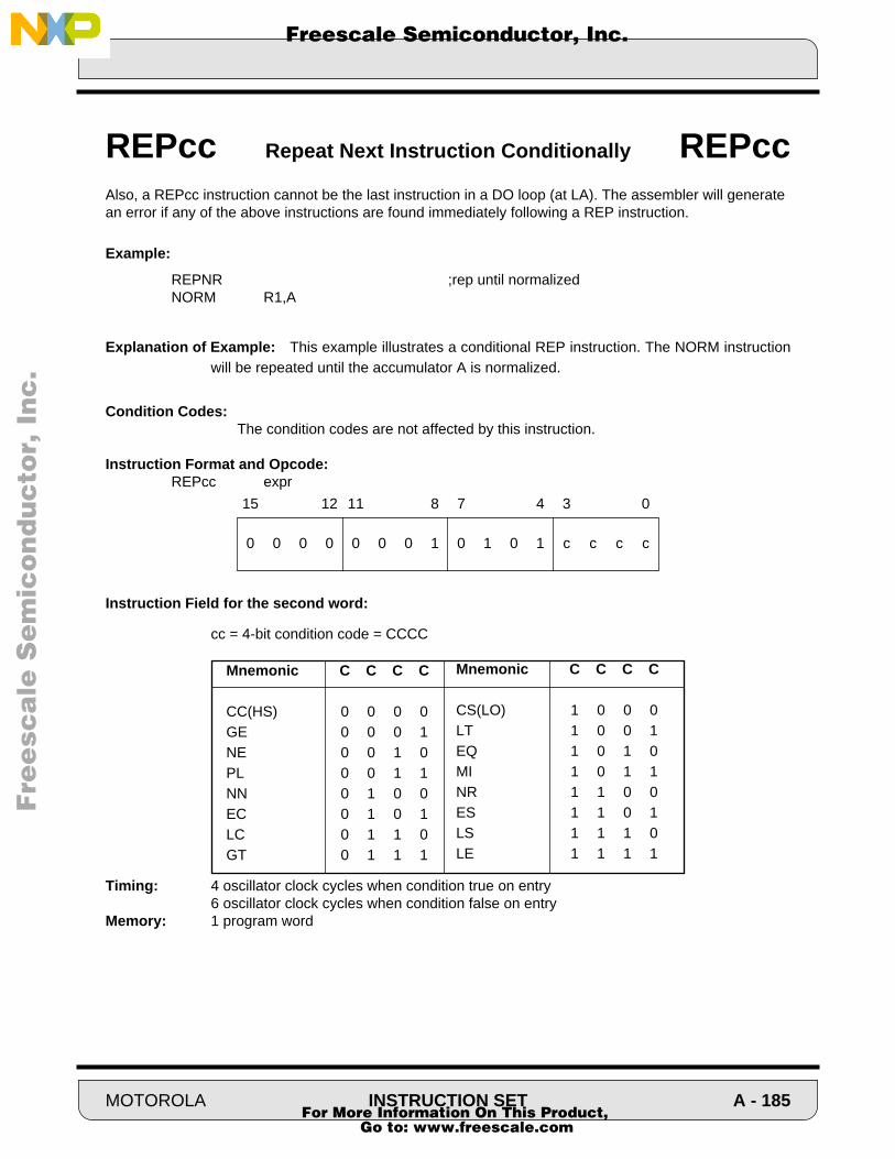
F
ree
sca
le S
em
ico
nd
uc
tor,
I
Freescale Semiconductor, Inc.n
c..
.
Also, a REPcc instruction cannot be the last instruction in a DO loop (at LA). The assembler will generate an error if any of the above instructions are found immediately following a REP instruction.
Example:
REPNR ;rep until normalizedNORM R1,A
Explanation of Example: This example illustrates a conditional REP instruction. The NORM instructionwill be repeated until the accumulator A is normalized.
Condition Codes:The condition codes are not affected by this instruction.
Instruction Format and Opcode:REPcc expr
Instruction Field for the second word:
cc = 4-bit condition code = CCCC
Timing: 4 oscillator clock cycles when condition true on entry6 oscillator clock cycles when condition false on entry
Memory: 1 program word
REPcc Repeat Next Instruction Conditionally REPcc
0 0 0 0 0 0 0 1 0 1 0 1 c c c c
15 12 11 8 7 4 3 0
Mnemonic C C C C
CC(HS) 0 0 0 0GE 0 0 0 1NE 0 0 1 0PL 0 0 1 1NN 0 1 0 0EC 0 1 0 1LC 0 1 1 0GT 0 1 1 1
Mnemonic C C C C
CS(LO) 1 0 0 0LT 1 0 0 1EQ 1 0 1 0MI 1 0 1 1NR 1 1 0 0ES 1 1 0 1LS 1 1 1 0LE 1 1 1 1
MOTOROLA INSTRUCTION SET A - 185 For More Information On This Product,
Go to: www.freescale.com

F
ree
sca
le S
em
ico
nd
uc
tor,
I
Freescale Semiconductor, Inc.n
c..
.
Operation: Assembler Syntax:
Reset the Interrupt Priority Register and all on-chip peripherals RESET
Description: Reset the Interrupt Priority Register and all on-chip peripherals. This is a software resetwhich is not equivalent to a hardware reset since only on-chip peripherals and the interruptstructure are affected. The processor state is not affected and execution continues with thenext instruction. All interrupt sources are disabled except for the trace, stack error, and re-set interrupts.
Restrictions:
A RESET instruction cannot be the last instruction in a DO loop (at LA).
Example:
RESET ;reset all on-chip peripherals and IPR, set I1,I0
Explanation of Example: Execution of the RESET instruction resets all on-chip peripherals and the In-terrupt Priority Register (IPR).
Condition Codes Affected:The condition codes are not affected by this instruction.
RESET RESET On-Chip Peripherals RESET
A - 186 INSTRUCTION SET MOTOROLA For More Information On This Product,
Go to: www.freescale.com
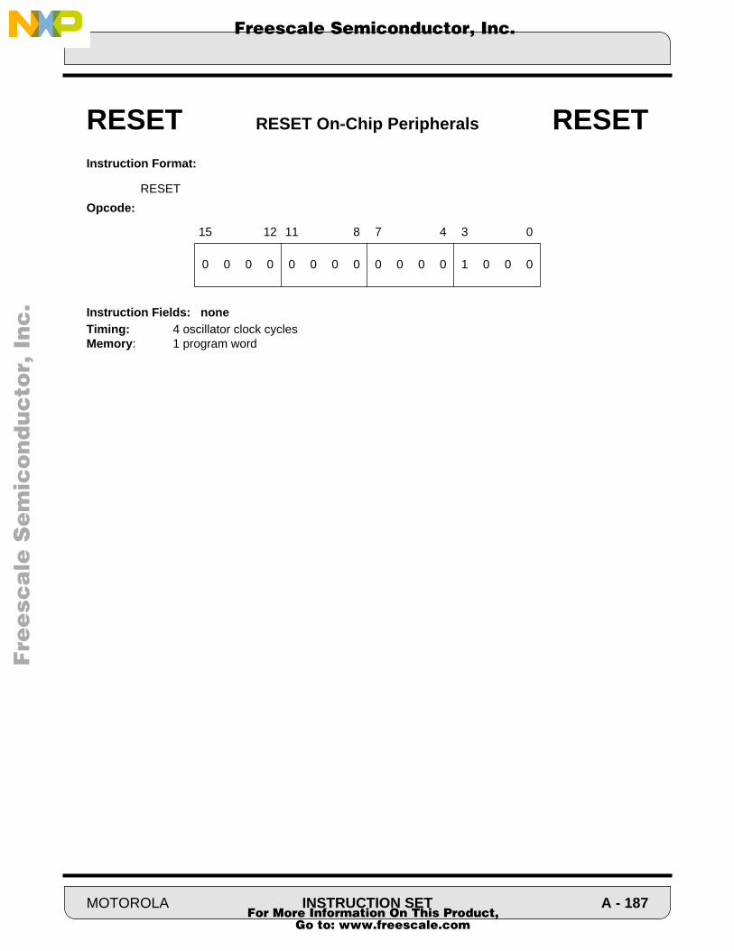
F
ree
sca
le S
em
ico
nd
uc
tor,
I
Freescale Semiconductor, Inc.n
c..
.
Instruction Format:
RESET
Opcode:
Instruction Fields: noneTiming: 4 oscillator clock cyclesMemory: 1 program word
RESET RESET On-Chip Peripherals RESET
0 0 0 0 0 0 0 0 0 0 0 0 1 0 0 0
15 12 11 8 7 4 3 0
MOTOROLA INSTRUCTION SET A - 187 For More Information On This Product,
Go to: www.freescale.com

F
ree
sca
le S
em
ico
nd
uc
tor,
I
Freescale Semiconductor, Inc.n
c..
.
Operation: Assembler Syntax:
D + r → D (parallel move) RND D (parallel move)
Description: Round the 40-bit value in the specified destination operand D and store the result in theMSP portion of the destination accumulator (A1 or B1). This instruction uses the roundingtechnique selected by the R bit in the Operating Mode Register (OMR). When the R bit inOMR is cleared (default mode), the convergent rounding is selected. When the R bit ofOMR is set, the twos-complement rounding is selected. The value of the rounding constantadded is determined by the scaling mode bits S0 and S1 in the system status register (SR).Refer to Section 3.2.5 for more information about the rounding modes.
Example:
RND A B,Y1 ;round A accumulator into A1, zero A0, save B1 first
Explanation of Example: Prior to execution, the 40-bit A accumulator contains the value $00:1236:789Afor Case I, the value $00:1236:8000 for Case II and the value $00:1235:8000 for Case III.Execution of the RND A instruction rounds the value in the A accumulator into the MSP por-tion of the A accumulator (A1) and then zeros the LSP portion of the A accumulator (A0).The example is given assuming that the convergent rounding is selected. Note that case IIis the special case that distinguishes convergent rounding from the twos complementrounding.
RND Round Accumulator RND
After Execution
00 1236 0000
A2 A1 A0
Before Execution
00 1236 789A
A2 A1 A0
After Execution
00 1236 0000
A2 A1 A0
Before Execution
00 1236 8000
A2 A1 A0
After Execution
00 1236 0000
A2 A1 A0
Before Execution
00 1235 8000
A2 A1 A0
I
II
III
A - 188 INSTRUCTION SET MOTOROLA For More Information On This Product,
Go to: www.freescale.com

F
ree
sca
le S
em
ico
nd
uc
tor,
I
Freescale Semiconductor, Inc.n
c..
.
Condition Codes:
S — Computed according to the standard definition (see section A.4)L — Set if limiting (parallel move) or overflow has occurred in resultE — Set if the signed integer portion of A or B result is in useU — Set according to the standard definition of the U bitN — Set if bit 39 of A or B result is setZ — Set if A or B result equals zeroV — Set if overflow has occurred in A or B result
Note: The definition of the E and U bits varies according to the scaling mode being used. Please refer toSection A.4 entitled “Condition Code Computation” for complete details.
Instruction Format:
RND D (parallel move)
Opcode:
Instruction Fields: Please see the “X Memory Data Move” description in the parallel move section for details on the m, RR, HHH, and W data fields.
Timing: 2 + mv oscillator clock cyclesMemory: 1 program word
RND Round Accumulator RND
15 14 13 12 11 10 9 8 7 6 5 4 3 2 1 0
LF * * * S1 S0 I1 I0 S L E U N Z V C
CCRMR
1 m R R H H H W 0 0 1 0 F 0 0 0
15 12 11 8 7 4 3 0
D F
A 0B 1
MOTOROLA INSTRUCTION SET A - 189 For More Information On This Product,
Go to: www.freescale.com

F
ree
sca
le S
em
ico
nd
uc
tor,
I
Freescale Semiconductor, Inc.n
c..
.
Assembler Syntax:
ROL D (parallel move)
Operation:
Description: Rotate bits 31-16 of the destination operand D one bit to the left and store the result in thedestination accumulator. Bit 31 of D prior to instruction execution is shifted into the carry bitC and the value in the carry bit C prior to instruction execution is shifted into bit 16 of thedestination accumulator D. This instruction is a 16-bit operation. The remaining bits of thedestination operand D are not affected.
Example:
ROL A (R3)- ;rotate A1 left one bit, update R3
Explanation of Example: Prior to execution, the 40-bit A accumulator contains the value$FE:0000:1234. Execution of the ROL A instruction shifts the 16-bit value in the A1 registerone bit to the left, shifting bit 31 into the carry bit C, rotating the carry bit C into bit 16, andstoring the result back in the A1 register.
ROL Rotate Left ROL
unch. unchanged (parallel move)
D2 D1 D0
C
0001
SR=MR:CCR
0000
SR=MR:CCR
After Execution
FE 0001 1234
A2 A1 A0
Before Execution
FE 0000 1234
A2 A1 A0
A - 190 INSTRUCTION SET MOTOROLA For More Information On This Product,
Go to: www.freescale.com
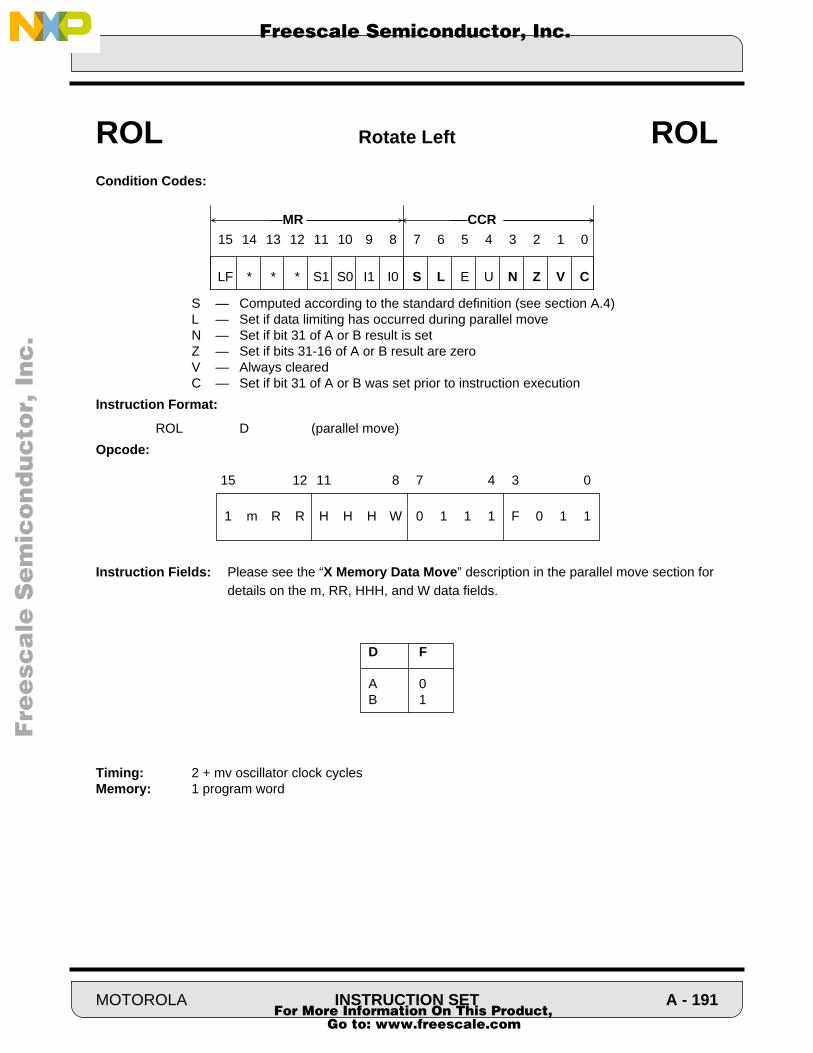
F
ree
sca
le S
em
ico
nd
uc
tor,
I
Freescale Semiconductor, Inc.n
c..
.
Condition Codes:
S — Computed according to the standard definition (see section A.4)L — Set if data limiting has occurred during parallel moveN — Set if bit 31 of A or B result is setZ — Set if bits 31-16 of A or B result are zeroV — Always clearedC — Set if bit 31 of A or B was set prior to instruction execution
Instruction Format:
ROL D (parallel move)
Opcode:
Instruction Fields: Please see the “X Memory Data Move” description in the parallel move section for details on the m, RR, HHH, and W data fields.
Timing: 2 + mv oscillator clock cyclesMemory: 1 program word
ROL Rotate Left ROL
15 14 13 12 11 10 9 8 7 6 5 4 3 2 1 0
LF * * * S1 S0 I1 I0 S L E U N Z V C
CCRMR
1 m R R H H H W 0 1 1 1 F 0 1 1
15 12 11 8 7 4 3 0
D F
A 0B 1
MOTOROLA INSTRUCTION SET A - 191 For More Information On This Product,
Go to: www.freescale.com

F
ree
sca
le S
em
ico
nd
uc
tor,
I
Freescale Semiconductor, Inc.n
c..
.
Assembler Syntax:
ROR D (parallel move)
Operation:
Description: Rotate bits 31-16 of the destination operand D one bit to the right and store the result in thedestination accumulator. Bit 16 of D prior to instruction execution is shifted into the carry bitC and the value in the carry bit C prior to instruction execution is shifted into bit 31 of thedestination accumulator D. This instruction is a 16-bit operation. The remaining bits of thedestination operand D are not affected.
Example:
ROR B (R2)+N2 ;rotate B1 right one bit, update R2
Explanation of Example: Prior to execution, the 40-bit B accumulator contains the value $00:0001:1234.Execution of the ROR B instruction shifts the 16-bit value in the B1 register one bit to theright, shifting bit 16 into the carry bit C, rotating the carry bit C into bit 31, and storing theresult back in the B1 register.
ROR Rotate Right ROR
unch. unchanged (parallel move)
D2 D1 D0
C
0000
SR=MR:CCR
0005
SR=MR:CCR
After Execution
FE 0000 1234
B2 B1 B0
Before Execution
FE 0001 1234
B2 B1 B0
A - 192 INSTRUCTION SET MOTOROLA For More Information On This Product,
Go to: www.freescale.com
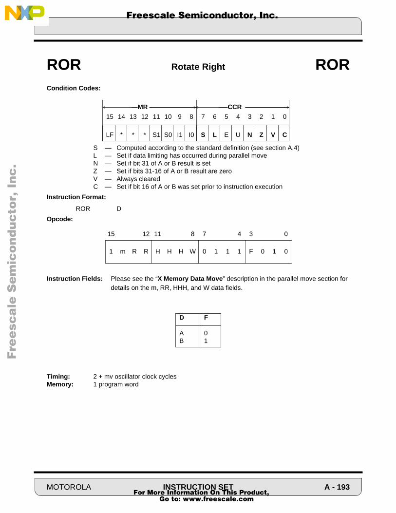
F
ree
sca
le S
em
ico
nd
uc
tor,
I
Freescale Semiconductor, Inc.n
c..
.
Condition Codes:
S — Computed according to the standard definition (see section A.4)L — Set if data limiting has occurred during parallel moveN — Set if bit 31 of A or B result is setZ — Set if bits 31-16 of A or B result are zeroV — Always clearedC — Set if bit 16 of A or B was set prior to instruction execution
Instruction Format:
ROR D
Opcode:
Instruction Fields: Please see the “X Memory Data Move” description in the parallel move section for details on the m, RR, HHH, and W data fields.
Timing: 2 + mv oscillator clock cyclesMemory: 1 program word
ROR Rotate Right ROR
15 14 13 12 11 10 9 8 7 6 5 4 3 2 1 0
LF * * * S1 S0 I1 I0 S L E U N Z V C
CCRMR
1 m R R H H H W 0 1 1 1 F 0 1 0
15 12 11 8 7 4 3 0
D F
A 0B 1
MOTOROLA INSTRUCTION SET A - 193 For More Information On This Product,
Go to: www.freescale.com
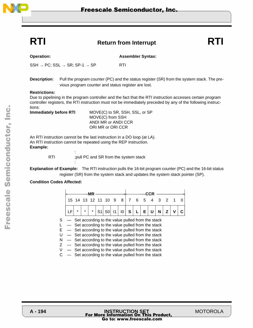
F
ree
sca
le S
em
ico
nd
uc
tor,
I
Freescale Semiconductor, Inc.n
c..
.
Operation: Assembler Syntax:
SSH → PC; SSL → SR; SP-1 → SP RTI
Description: Pull the program counter (PC) and the status register (SR) from the system stack. The pre-vious program counter and status register are lost.
Restrictions:Due to pipelining in the program controller and the fact that the RTI instruction accesses certain program controller registers, the RTI instruction must not be immediately preceded by any of the following instruc-tions:Immediately before RTI MOVE(C) to SR, SSH, SSL, or SP
MOVE(C) from SSHANDI MR or ANDI CCRORI MR or ORI CCR
An RTI instruction cannot be the last instruction in a DO loop (at LA).An RTI instruction cannot be repeated using the REP instruction.Example:
:RTI ;pull PC and SR from the system stack
:
Explanation of Example: The RTI instruction pulls the 16-bit program counter (PC) and the 16-bit statusregister (SR) from the system stack and updates the system stack pointer (SP).
Condition Codes Affected:
S — Set according to the value pulled from the stackL — Set according to the value pulled from the stackE — Set according to the value pulled from the stackU — Set according to the value pulled from the stackN — Set according to the value pulled from the stackZ — Set according to the value pulled from the stackV — Set according to the value pulled from the stackC — Set according to the value pulled from the stack
RTI Return from Interrupt RTI
15 14 13 12 11 10 9 8 7 6 5 4 3 2 1 0
LF * * * S1 S0 I1 I0 S L E U N Z V C
CCRMR
A - 194 INSTRUCTION SET MOTOROLA For More Information On This Product,
Go to: www.freescale.com
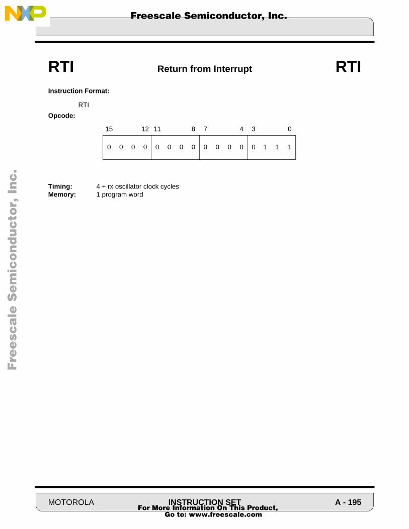
F
ree
sca
le S
em
ico
nd
uc
tor,
I
Freescale Semiconductor, Inc.n
c..
.
Instruction Format:
RTI
Opcode:
Timing: 4 + rx oscillator clock cyclesMemory: 1 program word
RTI Return from Interrupt RTI
0 0 0 0 0 0 0 0 0 0 0 0 0 1 1 1
15 12 11 8 7 4 3 0
MOTOROLA INSTRUCTION SET A - 195 For More Information On This Product,
Go to: www.freescale.com
F
ree
sca
le S
em
ico
nd
uc
tor,
I
Freescale Semiconductor, Inc.n
c..
.
Operation: Assembler Syntax:
SSH → PC; SP-1→ SP RTS
Description: Pull the program counter (PC) from the system stack. The previous program counter is lost.The status register (SR) is not affected.
Restrictions:
Due to pipelining in the program controller and the fact that the RTS instruction accesses certain programcontroller registers, the RTS instruction must not be immediately preceded by any of the following instruc-tions:
Immediately before RTS MOVE(C) to SSH, SSL, or SPMOVE(M) to SSH, SSL, or SPMOVE(P) to SSH, SSL, or SPMOVE(C) from SSHMOVE(M) from SSHMOVE(P) from SSH
An RTS instruction cannot be the last instruction in a DO loop (at LA).An RTS instruction cannot be repeated using the REP instruction.
Example:
RTS ;pull PC from the system stack
Explanation of Example: The RTS instruction pulls the 16-bit program counter (PC) from the systemstack and updates the system stack pointer (SP).
Condition Codes Affected:The condition codes are not affected by this instruction.
RTS Return from Subroutine RTS
A - 196 INSTRUCTION SET MOTOROLA For More Information On This Product,
Go to: www.freescale.com

F
ree
sca
le S
em
ico
nd
uc
tor,
I
Freescale Semiconductor, Inc.n
c..
.
Instruction Format:
RTS
Opcode:
Timing: 4 + rx oscillator clock cyclesMemory: 1 program word
RTS Return from Subroutine RTS
0 0 0 0 0 0 0 0 0 0 0 0 0 1 1 0
15 12 11 8 7 4 3 0
MOTOROLA INSTRUCTION SET A - 197 For More Information On This Product,
Go to: www.freescale.com

F
ree
sca
le S
em
ico
nd
uc
tor,
I
Freescale Semiconductor, Inc.n
c..
.
Operation: Assembler Syntax:
D - S - C → D (parallel move) SBC S,D (parallel move)
Description: Subtract the source operand S and the carry bit C of the condition code register from thedestination operand D and store the result in the destination accumulator. Long words (32bits) may be subtracted from the (40-bit) destination accumulator.
Note: The carry bit is set correctly for multiple precision arithmetic using long word operands if the exten-sion register of the destination accumulator (A2 or B2) is the sign extension of bit 31 of the destination ac-cumulator (A or B).
Example:
; 64 bit substraction: Y1:Y0:X1:X0 - B2:B1:B0:A1:A0 = B2:B1:B0:A1:A0
SUB X,A ;subtract LS wordsSBC Y,B ;subtract MS words with carry
Explanation of Example: This example illustrates long word double precision (64-bit) subtraction usingthe SBC instruction. Prior to execution of the SUB and SBC instructions, the 64-bit value$0000:0001:8000:0000 is loaded into the Y and X registers (Y:X), respectively. The otherdouble precision 64-bit value $0000:0003:0000:0000 is loaded into the B and A accumula-tors (B:A), respectively. Since the 32-bit value loaded into the A accumulator is automati-cally sign extended to 40-bits and the other 32-bit long word operand is internally sign ex-tended to 40-bits during instruction execution, the carry bit will be set correctly after the ex-ecution of the SUB X,A instruction. The SBC Y,B instruction then produces the correct MS40-bit result.
SBC Subtract Long with Carry SBC
A Before Execution
00 0000 0000
A2 A1 A0
B Before Execution
00 0000 0003
B2 B1 B0
A After Execution
00 8000 0000
A2 A1 A0
B After Execution
00 0000 0001
B2 B1 B0
8000 0000
X1 X0(X1:X0 not affected by operation)
0000 0001
Y1 Y0(Y1:Y0 not affected by operation)
A - 198 INSTRUCTION SET MOTOROLA For More Information On This Product,
Go to: www.freescale.com

F
ree
sca
le S
em
ico
nd
uc
tor,
I
Freescale Semiconductor, Inc.n
c..
.
Condition Codes Affected:
S — Computed according to the standard definition (see section A.4)L — Set if limiting (parallel move) or overflow has occurred in resultE — Set if the signed integer portion of A or B result is in useU — Set according to the standard definition of the U bitN — Set if bit 39 of A or B result is setZ — Set if A or B result equals zero. Cleared otherwiseV — Set if overflow has occurred in A or B resultC — Set if a carry (or borrow) occurs from bit 39 of A or B result
Note: The definition of the E and U bits varies according to the scaling mode being used. Please refer toSection A.4 entitled “Condition Code Computation” for complete details.
Instruction Format:
SBC S,D (parallel move)
Opcode:
Instruction Fields: Please see the “X Memory Data Move” description in the parallel move section for details on the m, RR, HHH, and W data fields.
Timing: 2+mv oscillator clock cyclesMemory: 1 program word
SBC Subtract Long with Carry SBC
15 14 13 12 11 10 9 8 7 6 5 4 3 2 1 0
LF * * * S1 S0 I1 I0 S L E U N Z V C
CCRMR
1 m R R H H H W 0 1 0 1 F 0 1 J
15 12 11 8 7 4 3 0
S,D J F
X,A 0 0X,B 0 1Y,A 1 0Y,B 1 1
MOTOROLA INSTRUCTION SET A - 199 For More Information On This Product,
Go to: www.freescale.com

F
ree
sca
le S
em
ico
nd
uc
tor,
I
Freescale Semiconductor, Inc.n
c..
.
Operation: Assembler Syntax:
Enter the STOP processing state and stop the clock oscillator STOP
Description: Enter the STOP processing state. All activity in the processor is suspended until the RESET
or IRQA pin is asserted. The STOP processing state is a low-power standby mode.
During the STOP state, port A is in an idle state with the control signals held inactive (i.e.,PS/DS=VCC etc.), the data pins (D0-D23) are high impedance, and the address pins (A1-A15) are unchanged from the previous instruction. If the bus grant was asserted when theSTOP instruction was executed, port A will remain three-stated until the DSP exits theSTOP state.
When the exit from the stop state is caused by a low level on the RESET pin, then the pro-cessor will enter the reset processing state. The time to recover from the STOP state usingRESET will depend on a clock stabilization delay controlled by the SD bit in the OMR.
When the exit from the stop state is caused by a low level on the IRQA pin, then the pro-cessor will service the highest priority pending interrupt and will not service the IRQA inter-rupt unless it is highest priority. The interrupt will be serviced after an internal delay countercounts 524,284 clock phases (i.e., [219-4]T) or 28 clock phases (i.e., [25-4]T) delay if thestop delay (SD) bit in the OMR is set to one. During this clock stabilization count delay, allperipherals and external interrupts are cleared and re-enabled/arbitrated at the start of the17T period following the count interval. The processor will resume program execution at theinstruction following the STOP instruction that caused the entry into the stop state after theinterrupts have been serviced or, if no interrupt was pending, immediately after the delaycount plus 17T. If the IRQA pin is asserted when the STOP instruction is executed the in-ternal delay counter will be started. Refer to Section 7.6 for details on the STOP mode.
Restrictions:
— A STOP instruction cannot be used in a fast interrupt routine.— A STOP instruction cannot be the last instruction in a DO loop (i.e., at LA).— A STOP instruction cannot be repeated using the REP instruction.
Example:
STOP ;enter low-power standby mode
Explanation of Example: The STOP instruction suspends all processor activity until the processor is re-set or interrupted as previously described. The STOP instruction puts the processor in alow-power standby mode.
Condition Codes Affected:The condition codes are not affected by this instruction.
STOP Stop Instruction Processing STOP
A - 200 INSTRUCTION SET MOTOROLA For More Information On This Product,
Go to: www.freescale.com

F
ree
sca
le S
em
ico
nd
uc
tor,
I
Freescale Semiconductor, Inc.n
c..
.
Instruction Format:
STOP
Opcode:
Instruction Fields: None
Timing: The STOP instruction disables internal distribution of the clock.
Memory: 1 program word
STOP Stop Instruction Processing STOP
0 0 0 0 0 0 0 0 0 0 0 0 1 0 1 0
15 12 11 8 7 4 3 0
MOTOROLA INSTRUCTION SET A - 201 For More Information On This Product,
Go to: www.freescale.com
F
ree
sca
le S
em
ico
nd
uc
tor,
I
Freescale Semiconductor, Inc.n
c..
.
Operation Assembler Syntax:
D - S → D (parallel move) SUB S,D (parallel move)D - S → D (two parallel reads) SUB S,D (two parallel reads)
Description: Subtract the source operand S from the destination operand D and store the result in thedestination operand D. Words (16 bits), long words (32 bits) and accumulators (40 bits)may be subtracted from the destination accumulator.
Note: The carry bit is set correctly using word or long word source operands if the extension register ofthe destination accumulator (A2 or B2) is the sign extension of bit 31 of the destination accumulator (A orB). The carry bit is always set correctly using accumulator source operands.
Example:
SUB X1,A X:(R2)+N2,X0 ;16-bit subtract, load X0, update R2
Explanation of Example: Prior to execution, the 16-bit X1 register contains the value $0003 and the 40-bit A accumulator contains the value $00:0058:1234. The SUB instruction automatically ap-pends the16-bit value in the X1 register with 16 LS zeros, sign extends the resulting 32-bitlong word to 40 bits, and subtracts the result from the 40-bit A accumulator. Thus, 16-bitoperands are subtracted from the MSP portion of A or B (A1 or B1) because all arithmeticinstructions assume a fractional, two’s complement data representation. Note that 16-bitoperands can be subtracted from the LSP portion of A or B (A0 or B0) by loading the 16-bitoperand into X0 or Y0, forming a 32-bit word by loading X1 or Y1 with the sign extensionof X0 or Y0, and executing a SUB X,A or SUB Y,A instruction.
SUB Subtract SUB
After Execution
00 0055 1234
A2 A1 A0
Before Execution
00 0058 1234
A2 A1 A0
0003
X1
0003
X1
A - 202 INSTRUCTION SET MOTOROLA For More Information On This Product,
Go to: www.freescale.com
F
ree
sca
le S
em
ico
nd
uc
tor,
I
Freescale Semiconductor, Inc.n
c..
.
Condition Codes:
S — Computed according to the standard definition (see section A.4)L — Set if limiting (parallel move) or overflow has occurred in resultE — Set if the signed integer portion of A or B result is in useU — Set according to the standard definition of the U bitN — Set if bit 39 of A or B result is setZ — Set if A or B result equals zeroV — Set if overflow has occurred in A or B resultC — Set if a carry (or borrow) occurs from bit 39 of A or B result
Note: The definition of the E and U bits varies according to the scaling mode being used. Please refer toSection A.4 entitled “Condition Code Computation” for complete details.
Instruction Format: SUB S,D (parallel move)
Opcode:
Timing: 2 + mv oscillator clock cyclesMemory: 1 program word
SUB Subtract SUB
15 14 13 12 11 10 9 8 7 6 5 4 3 2 1 0
LF * * * S1 S0 I1 I0 S L E U N Z V C
CCRMR
1 m R R H H H W 0 1 0 0 F J J J
15 12 11 8 7 4 3 0
0 1 1 m m K K K 0 r r u F u u u
15 12 11 8 7 4 3 0
Instruction Format: SUB S,D (two parallel reads)Opcode:
Instruction Fields: Please see the “X Memory Data Move” description in the parallel move section fordetails on the m, RR, HHH, W, and mm data fields.
Instruction Fields: Please see the “Dual X Memory Data Read” description in the parallel move sec-tion for details on the mm and KKK data fields.
S,D J J J FB,A 0 0 0 0A,B 0 0 0 1X,A 0 1 0 0X,B 0 1 0 1Y,A 0 1 1 0Y,B 0 1 1 1X0,A 1 0 0 0
S,D J J J FX0,B 1 0 0 1Y0,A 1 0 1 0Y0,B 1 0 1 1X1,A 1 1 0 0X1,B 1 1 0 1Y1,A 1 1 1 0Y1,B 1 1 1 1
S,D u u u u FX0,A 0 1 0 0 0X0,B 0 1 0 0 1Y0,A 0 1 0 1 0Y0,B 0 1 0 1 1X1,A 0 1 1 0 0X1,B 0 1 1 0 1Y1,A 0 1 1 1 0
One Parallel Operation Two Parallel ReadsS,D u u u u FY1,B 0 1 1 1 1
B,A 1 1 0 1 0A,B 1 1 0 1 1
MOTOROLA INSTRUCTION SET A - 203 For More Information On This Product,
Go to: www.freescale.com
F
ree
sca
le S
em
ico
nd
uc
tor,
I
Freescale Semiconductor, Inc.n
c..
.
Operation: Assembler Syntax:
D* 2 - S → D (parallel move) SUBL S,D (parallel move)
Description: Subtract the source operand S from two times the destination operand D and store the re-sult in the destination accumulator. The destination operand D is arithmetically shifted onebit to the left and a zero is shifted into the LS bit of D prior to the subtraction operation. Thecarry bit is set correctly if the source operand does not overflow as a result of the left shiftoperation. The overflow bit may be set as a result of either the shifting or subtraction oper-ation (or both). This instruction is useful for efficient divide and decimation in time (DIT) FFTalgorithms.
Example:
SUBL B,A X:(R3)+,X1 ;A * 2 - B → A, updateX1 and R3
Explanation of Example: Prior to execution, the 40-bit A accumulator contains the value $00:0000:2468and the 40-bit B accumulator contains the value $00:0000:1234. The SUBL B,A instructionsubtracts the value in the B accumulator from two times the value in the A accumulator andstores the 40-bit result in the A accumulator.
Condition Codes Affected:
S — Computed according to the standard definition (see section A.4)L — Set if limiting (parallel move) or overflow has occurred in resultE — Set if the signed integer portion of A or B result is in useU — Set according to the standard definition of the U bitN — Set if bit 39 of A or B result is setZ — Set if A or B result equals zeroV — Set if overflow has occurred in A or B result or if the MSB of the destination
operand is changed as a result of the instruction’s left shift.C — Set if a carry (or borrow) occurs from bit 39 of A or B result
Note: The definition of the E and U bits varies according to the scaling mode being used. Please refer toSection A.4 entitled “Condition Code Computation” for complete details.
SUBL Shift Left and Subtract Accumulators SUBL
After Execution
00 0000 369C
A2 A1 A0
Before Execution
00 0000 2468
A2 A1 A0
00 0000 1234
B2 B1 B0
00 0000 1234
B2 B1 B0
15 14 13 12 11 10 9 8 7 6 5 4 3 2 1 0
LF * * * S1 S0 I1 I0 S L E U N Z V C
CCRMR
A - 204 INSTRUCTION SET MOTOROLA For More Information On This Product,
Go to: www.freescale.com

F
ree
sca
le S
em
ico
nd
uc
tor,
I
Freescale Semiconductor, Inc.n
c..
.
Instruction Format:
SUBL S,D (parallel move)Opcode:
Instruction Fields
Timing: 2 + mv oscillator clock cyclesMemory: 1 program word
SUBL Shift Left and Subtract Accumulators SUBL
1 m R R H H H W 0 1 0 0 F 0 0 1
15 12 11 8 7 4 3 0
Instruction Fields: Please see the “X Memory Data Move” description in the parallel move section fordetails on the m, RR, HHH, W, and mm data fields.
S,D F
B,A 0
MOTOROLA INSTRUCTION SET A - 205 For More Information On This Product,
Go to: www.freescale.com

F
ree
sca
le S
em
ico
nd
uc
tor,
I
Freescale Semiconductor, Inc.n
c..
.
Operation: Assembler Syntax:
D1 ↔ D0 (no parallel move) SWAP D (no parallel move)
Description: Exchange MS word and LS words of destination accumulator. The extension register is notaffected by this instruction.
Example:
SWAP A
Explanation of Example: Prior to execution, the 40-bit A accumulator contains the value$FE:0000:1234. Execution of the SWAP A instruction exchange the 16-bit value in the A1register with the 16-bit value in the A0 register.
Condition Codes Affected: The condition codes are not affected by this instruction.
SWAP Swap Accumulator Words SWAP
After Execution
FE 1234 0000
A2 A1 A0
Before Execution
FE 0000 1234
A2 A1 A0
A - 206 INSTRUCTION SET MOTOROLA For More Information On This Product,
Go to: www.freescale.com
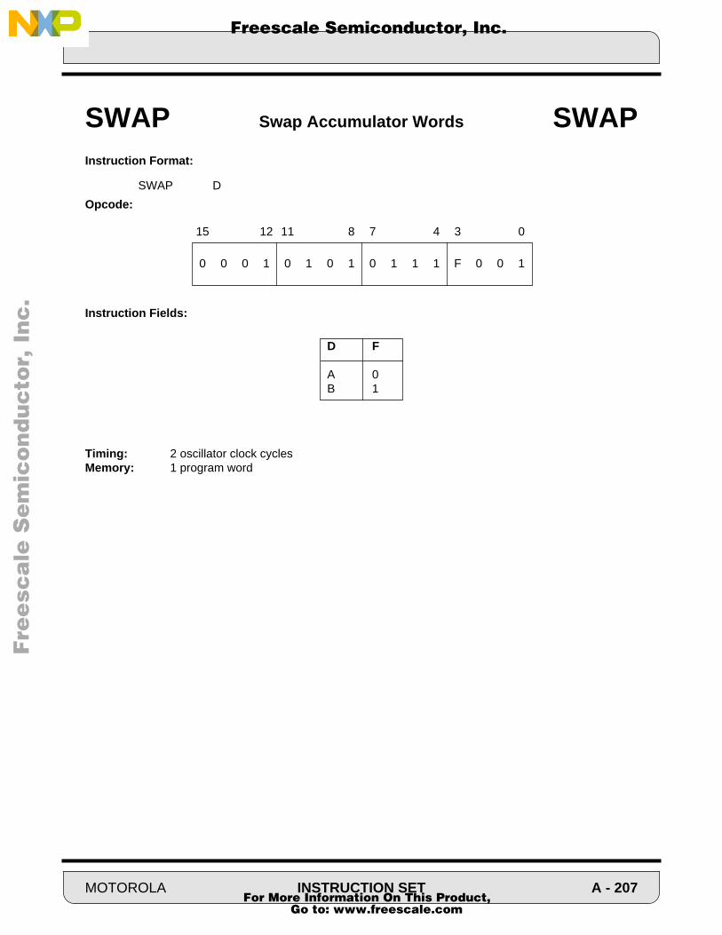
F
ree
sca
le S
em
ico
nd
uc
tor,
I
Freescale Semiconductor, Inc.n
c..
.
Instruction Format:
SWAP D
Opcode:
Instruction Fields:
Timing: 2 oscillator clock cyclesMemory: 1 program word
SWAP Swap Accumulator Words SWAP
0 0 0 1 0 1 0 1 0 1 1 1 F 0 0 1
15 12 11 8 7 4 3 0
D F
A 0B 1
MOTOROLA INSTRUCTION SET A - 207 For More Information On This Product,
Go to: www.freescale.com

F
ree
sca
le S
em
ico
nd
uc
tor,
I
Freescale Semiconductor, Inc.n
c..
.
Operation: Assembler Syntax:
Begin SWI exception processing SWI
Description: Suspend normal instruction execution and begin SWI exception processing. The interruptpriority level (I1,I0) is set to 3 in the status register (SR) if a long interrupt service routine isused.
Restrictions:
— A SWI instruction cannot be used in a fast interrupt routine.
— A SWI instruction cannot be repeated using the REP instruction.
Example:
:SWI ;begin SWI exception processing
Explanation of Example: The SWI instruction suspends normal instruction execution and initiates SWIexception processing.
Condition Codes Affected:The condition codes are not affected by this instruction.
SWI Software Interrupt SWI
A - 208 INSTRUCTION SET MOTOROLA For More Information On This Product,
Go to: www.freescale.com

F
ree
sca
le S
em
ico
nd
uc
tor,
I
Freescale Semiconductor, Inc.n
c..
.
Instruction Format:
SWIOpcode:
Instruction Fields: none
Timing: 8 oscillator clock cyclesMemory: 1 program word
SWI Software Interrupt SWI
0 0 0 0 0 0 0 0 0 0 0 0 0 1 0 1
15 12 11 8 7 4 3 0
MOTOROLA INSTRUCTION SET A - 209 For More Information On This Product,
Go to: www.freescale.com

F
ree
sca
le S
em
ico
nd
uc
tor,
I
Freescale Semiconductor, Inc.n
c..
.
Operation: Assembler Syntax:
If cc, then S → D Tcc (S,D)
If cc, then S → D and R0 → Rn Tcc S,D R0,Rn
Description: Transfer data from the specified source register S1 to the specified destination accumulatorD1 if the specified condition is true. If a second source register R0 and a second destinationregister Rn are also specified, transfer data from address register R0 to address registerRn if the specified condition is true. If the specified condition is false, a NOP is executed.
When used after the CMP or CMPM instructions, the Tcc instruction can perform many use-ful functions such as a “maximum value”, “minimum value”, “maximum absolute value”, or“minimum absolute value” function. The desired value is stored in the destination accumu-lator D. If address register R0 is used as an address pointer into an array of data, the ad-dress of the desired value is stored in the address register Rn. The Tcc instruction may beused after any instruction and allows efficient searching and sorting algorithms. Transfer-ring A to A or B to B conditionally updates a register without affecting the ALU registers.
The term “cc” may specify the following conditions:
where: U denotes the logical complement of U,+ denotes the logical OR operator,• denotes the logical AND operator,⊕ denotes the logical Exclusive OR operator
Note: This instruction is considered to be a move-type instruction. Due to pipelining, if an address register(R0-R3) is changed using a move-type instruction, the new contents of the destination address register willnot be available for use during the following instruction (i.e., there is a single instruction cycle pipeline delay).
Tcc Transfer Conditionally Tcc
“cc” Mnemonic Condition
CC (HS) — carry clear (higher or same) C=0CS (LO) — carry set(lower) C=1EC — extension clear E=0EQ — equal Z=1ES — extension set E=1GE — greater than or equal N ⊕ V=0GT — greater than Z+(N ⊕ V)=0LC — limit clear L=0LE — less than or equal Z+(N ⊕ V)=1LS — limit set L=1LT — less than N ⊕ V=1MI — minus N=1NE — not equal Z=0NR — normalized Z+(U•E)=1PL — plus N=0NN — not normalized Z+(U•E)=0
A - 210 INSTRUCTION SET MOTOROLA For More Information On This Product,
Go to: www.freescale.com

F
ree
sca
le S
em
ico
nd
uc
tor,
I
Freescale Semiconductor, Inc.n
c..
.
Example:
CMP X0,A ;compare X0 and A (sort for minimum)TLT X0,A R0,R1 ;transfer X0 → A and R0 → R1 if X0 < A
Explanation of Example: In this example, the contents of the 16-bit X0 register are transferred to the 40-bit A accumulator and the contents of the 16-bit R0 address register are transferred to the16-bit R1 address register if the specified condition is true. If the specified condition is nottrue, a NOP is executed.
Condition Codes Affected:The condition codes are not affected by this instruction.
Instruction Format:
Tcc S1,D1 R0,RnOpcode:
Instruction Fields:
* Encoding used by the assembler when no Data ALU transfer is specified in the instructioncc = 4-bit condition code = CCCC
Timing: 2 oscillator clock cyclesMemory: 1 program word
Tcc Transfer Conditionally Tcc
0 0 0 1 0 0 c c c c T T F h 0 h
15 12 11 8 7 4 3 0
S,D h0h F
X0,A 100 0X0,B 100 1Y0,A 101 0Y0,B 101 1
TT Rn
00 R001 R110 R211 R3
S,D h0h F
A,A* 001 0A,B 000 1B,A 000 0B,B 001 1
Mnemonic C C C C
CC(HS) 0 0 0 0GE 0 0 0 1NE 0 0 1 0PL 0 0 1 1NN 0 1 0 0EC 0 1 0 1LC 0 1 1 0GT 0 1 1 1
Mnemonic C C C C
CS(LO) 1 0 0 0LT 1 0 0 1EQ 1 0 1 0MI 1 0 1 1NR 1 1 0 0ES 1 1 0 1LS 1 1 1 0LE 1 1 1 1
MOTOROLA INSTRUCTION SET A - 211 For More Information On This Product,
Go to: www.freescale.com
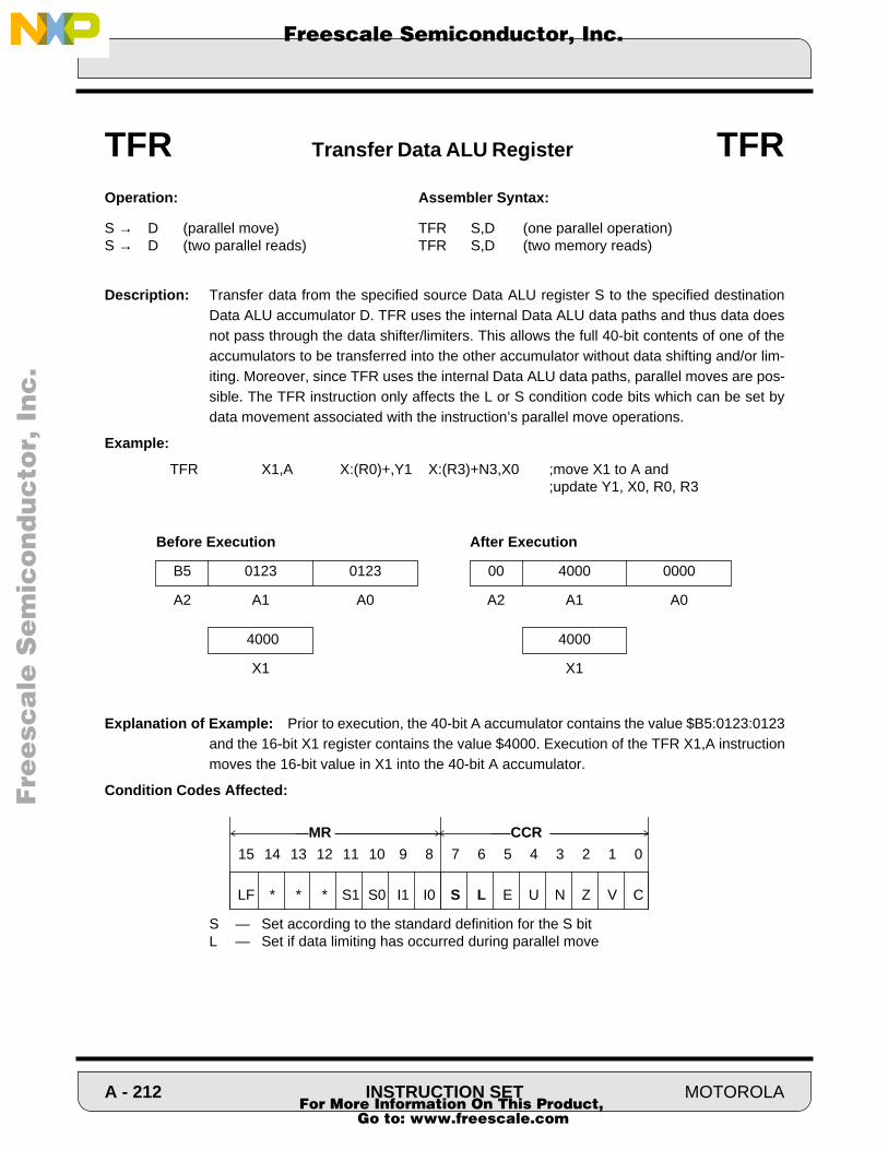
F
ree
sca
le S
em
ico
nd
uc
tor,
I
Freescale Semiconductor, Inc.n
c..
.
Operation: Assembler Syntax:
S → D (parallel move) TFR S,D (one parallel operation)S → D (two parallel reads) TFR S,D (two memory reads)
Description: Transfer data from the specified source Data ALU register S to the specified destinationData ALU accumulator D. TFR uses the internal Data ALU data paths and thus data doesnot pass through the data shifter/limiters. This allows the full 40-bit contents of one of theaccumulators to be transferred into the other accumulator without data shifting and/or lim-iting. Moreover, since TFR uses the internal Data ALU data paths, parallel moves are pos-sible. The TFR instruction only affects the L or S condition code bits which can be set bydata movement associated with the instruction’s parallel move operations.
Example:
TFR X1,A X:(R0)+,Y1 X:(R3)+N3,X0 ;move X1 to A and;update Y1, X0, R0, R3
Explanation of Example: Prior to execution, the 40-bit A accumulator contains the value $B5:0123:0123and the 16-bit X1 register contains the value $4000. Execution of the TFR X1,A instructionmoves the 16-bit value in X1 into the 40-bit A accumulator.
Condition Codes Affected:
S — Set according to the standard definition for the S bitL — Set if data limiting has occurred during parallel move
TFR Transfer Data ALU Register TFR
4000
X1
4000
X1
After Execution
00 4000 0000
A2 A1 A0
Before Execution
B5 0123 0123
A2 A1 A0
15 14 13 12 11 10 9 8 7 6 5 4 3 2 1 0
LF * * * S1 S0 I1 I0 S L E U N Z V C
CCRMR
A - 212 INSTRUCTION SET MOTOROLA For More Information On This Product,
Go to: www.freescale.com
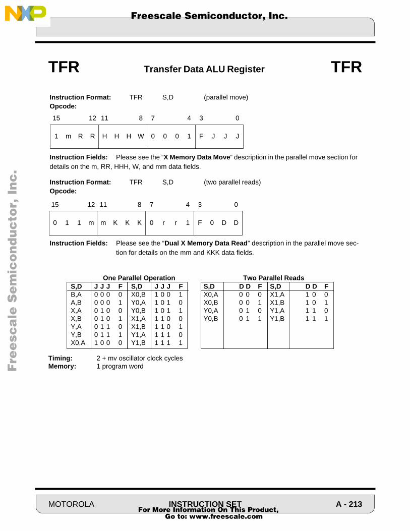
F
ree
sca
le S
em
ico
nd
uc
tor,
I
Freescale Semiconductor, Inc.n
c..
.
Timing: 2 + mv oscillator clock cyclesMemory: 1 program word
TFR Transfer Data ALU Register TFR
1 m R R H H H W 0 0 0 1 F J J J
15 12 11 8 7 4 3 0
0 1 1 m m K K K 0 r r 1 F 0 D D
15 12 11 8 7 4 3 0
Instruction Fields: Please see the “X Memory Data Move” description in the parallel move section fordetails on the m, RR, HHH, W, and mm data fields.
Instruction Format: TFR S,D (parallel move)Opcode:
Instruction Format: TFR S,D (two parallel reads)Opcode:
Instruction Fields: Please see the “Dual X Memory Data Read” description in the parallel move sec-tion for details on the mm and KKK data fields.
S,D J J J FB,A 0 0 0 0A,B 0 0 0 1X,A 0 1 0 0X,B 0 1 0 1Y,A 0 1 1 0Y,B 0 1 1 1X0,A 1 0 0 0
S,D J J J FX0,B 1 0 0 1Y0,A 1 0 1 0Y0,B 1 0 1 1X1,A 1 1 0 0X1,B 1 1 0 1Y1,A 1 1 1 0Y1,B 1 1 1 1
S,D D D FX0,A 0 0 0X0,B 0 0 1Y0,A 0 1 0Y0,B 0 1 1
One Parallel Operation Two Parallel ReadsS,D D D FX1,A 1 0 0X1,B 1 0 1Y1,A 1 1 0Y1,B 1 1 1
MOTOROLA INSTRUCTION SET A - 213 For More Information On This Product,
Go to: www.freescale.com

F
ree
sca
le S
em
ico
nd
uc
tor,
I
Freescale Semiconductor, Inc.n
c..
.
Operation: Assembler Syntax:
S → D (no parallel move) TFR(2) S,D (no parallel operation)
Description: Transfer data from the specified source accumulator S to the specified 32-bit destinationData ALU register D. GDB and XDB are used for this transfer. The transferred data passesthrough the shifter/limiter; therefore, the L condition code bit will be affected.
Example:
TFR(2) A,X ;move A to X1:X0
Explanation of Example: Prior to execution, the 40-bit A accumulator contains the value $FF:FFFF:0123and the 32-bit X1:X0 register contains the value $1234:5678. Execution of the TFR A,X in-struction moves the 32-bit value in A into the 32-bit X (X1:X0) register. The L bit is not set.
Condition Codes Affected:
L — Set if data limiting has occurred
TFR(2) Two Word Data ALU Register Transfer TFR(2)
FFFF
X1
1234
X1
0123
X0
After Execution
FF FFFF 0123
A2 A1 A0
Before Execution
FF FFFF 0123
A2 A1 A0
4567
X0
15 14 13 12 11 10 9 8 7 6 5 4 3 2 1 0
LF * * * S1 S0 I1 I0 S L E U N Z V C
CCRMR
A - 214 INSTRUCTION SET MOTOROLA For More Information On This Product,
Go to: www.freescale.com

F
ree
sca
le S
em
ico
nd
uc
tor,
I
Freescale Semiconductor, Inc.n
c..
.
Instruction Format:
TFR(2) S,D
Opcode:
Instruction Fields:
Timing: 2 oscillator clock cyclesMemory: 1 program word
TFR(2) Two Word Data ALU Register Transfer TFR(2)
0 0 0 1 0 1 0 1 0 0 0 0 F 0 0 J
15 12 11 8 7 4 3 0
S,D J F
A,X 0 0B,X 0 1A,Y 1 0B,Y 1 1
MOTOROLA INSTRUCTION SET A - 215 For More Information On This Product,
Go to: www.freescale.com
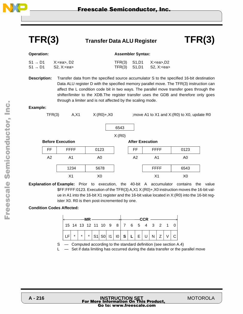
F
ree
sca
le S
em
ico
nd
uc
tor,
I
Freescale Semiconductor, Inc.n
c..
.
Operation: Assembler Syntax:
S1 → D1 X:<ea>, D2 TFR(3) S1,D1 X:<ea>,D2S1 → D1 S2, X:<ea> TFR(3) S1,D1 S2, X:<ea>
Description: Transfer data from the specified source accumulator S to the specified 16-bit destinationData ALU register D with the specified memory parallel move. The TFR(3) instruction canaffect the L condition code bit in two ways. The parallel move transfer goes through theshifter/limiter to the XDB.The register transfer uses the GDB and therefore only goesthrough a limiter and is not affected by the scaling mode.
Example:
TFR(3) A,X1 X:(R0)+,X0 ;move A1 to X1 and X:(R0) to X0, update R0
Explanation of Example: Prior to execution, the 40-bit A accumulator contains the value$FF:FFFF:0123. Execution of the TFR(3) A,X1 X:(R0)+,X0 instruction moves the 16-bit val-ue in A1 into the 16-bit X1 register and the 16-bit value located in X:(R0) into the 16-bit reg-ister X0. R0 is then post-incremented by one.
Condition Codes Affected:
S — Computed according to the standard definition (see section A.4)L — Set if data limiting has occurred during the data transfer or the parallel move
TFR(3) Transfer Data ALU Register TFR(3)
FFFF
X1
1234
X1
6543
X0
After Execution
FF FFFF 0123
A2 A1 A0
Before Execution
FF FFFF 0123
A2 A1 A0
5678
X0
6543
X:(R0)
15 14 13 12 11 10 9 8 7 6 5 4 3 2 1 0
LF * * * S1 S0 I1 I0 S L E U N Z V C
CCRMR
A - 216 INSTRUCTION SET MOTOROLA For More Information On This Product,
Go to: www.freescale.com
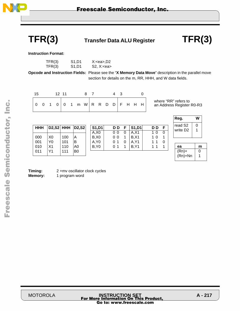
F
ree
sca
le S
em
ico
nd
uc
tor,
I
Freescale Semiconductor, Inc.n
c..
.
Instruction Format:
TFR(3) S1,D1 X:<ea>,D2TFR(3) S1,D1 S2, X:<ea>
Opcode and Instruction Fields: Please see the “X Memory Data Move” description in the parallel move section for details on the m, RR, HHH, and W data fields.
Timing: 2 +mv oscillator clock cyclesMemory: 1 program word
TFR(3) Transfer Data ALU Register TFR(3)
Reg. W
read S2 0write D2 1
0 0 1 0 0 1 m W R R D D F H H H
15 12 11 8 7 4 3 0
HHH D2,S2 HHH D2,S2
000 X0 100 A001 Y0 101 B010 X1 110 A0011 Y1 111 B0
S1,D1 D D FA,X0 0 0 0B,X0 0 0 1A,Y0 0 1 0B,Y0 0 1 1
S1,D1 D D FA,X1 1 0 0B,X1 1 0 1A,Y1 1 1 0B,Y1 1 1 1
where “RR” refers to an Address Register R0-R3
ea m(Rn)+ 0(Rn)+Nn 1
MOTOROLA INSTRUCTION SET A - 217 For More Information On This Product,
Go to: www.freescale.com

F
ree
sca
le S
em
ico
nd
uc
tor,
I
Freescale Semiconductor, Inc.n
c..
.
Operation: Assembler Syntax:
S - 0 (parallel move) TST S (parallel move)
Description: Compare the specified source accumulator S with zero and set the condition codes accord-ingly. No result is stored although the condition codes are updated.
Example:
TST A X:(R0)+N0,B ;set CCR bits for value in A, update B and R0
Explanation of Example: Prior to execution, the 40-bit A accumulator contains the value $01:0203:0000and the 16-bit condition code register (CCR) contains the value $0300. Execution of theTST A instruction compares the value in the A register with zero and updates the conditioncode register accordingly. The contents of the A accumulator are not affected.
Condition Codes Affected:
S — Computed according to the standard definition (see section A.4)L — Set if data limiting has occurred during parallel moveE — Set if the signed integer portion of A or B result is in useU — Set according to the standard definition of the U bitN — Set if bit 39 of A or B result is setZ — Set if A or B result equals zeroV — Always clearedC — Always cleared
Note: The definition of the E and U bits varies according to the scaling mode being used. Please refer toSection A.4 entitled “Condition Code Computation” for complete details.
TST Test Accumulator TST
0300
SR=MR:CCR
0330
SR=MR:CCR
After Execution
01 0203 0000
A2 A1 A0
Before Execution
01 0203 0000
A2 A1 A0
15 14 13 12 11 10 9 8 7 6 5 4 3 2 1 0
LF * * * S1 S0 I1 I0 S L E U N Z V C
CCRMR
A - 218 INSTRUCTION SET MOTOROLA For More Information On This Product,
Go to: www.freescale.com

F
ree
sca
le S
em
ico
nd
uc
tor,
I
Freescale Semiconductor, Inc.n
c..
.
Instruction Format:
TST S (parallel move)
Opcode:
Instruction Fields: Please see the “X Memory Data Move” description in the parallel move section for details on the m, RR, HHH, and W data fields.
Timing: 2+mv oscillator clock cyclesMemory: 1 program word
TST Test Accumulator TST
1 m R R H H H W 0 0 1 0 F 0 0 1
15 12 11 8 7 4 3 0
S F
A 0B 1
MOTOROLA INSTRUCTION SET A - 219 For More Information On This Product,
Go to: www.freescale.com

F
ree
sca
le S
em
ico
nd
uc
tor,
I
Freescale Semiconductor, Inc.n
c..
.
Operation: Assembler Syntax:
S - 0 (no parallel move) TST(2) S (no parallel move)
Description: Compare the specified source Data ALU register S with zero and set the condition codesaccordingly. No result is stored although the condition codes are updated.
Example:
TST(2) X1 ;set CCR bits for value in X1
Explanation of Example: Prior to execution, the 16-bit X0 register contains the value #$0203 and the 16-bit condition code register (CCR) contains the value $0300. Execution of the TST(2) X0 in-struction compares the value in the X0 register with zero and updates the condition coderegister accordingly. The contents of the X0 register is not affected.
Condition Codes Affected:
U — Set if result is unnormalizedN — Set if bit 31 of A or B result is setZ — Set if result equals zeroC — Always cleared
TST(2) Test Data ALU Register TST(2)
0300
SR=MR:CCR
0310
SR=MR:CCR
Before Execution
0203
X1
After Execution
0203
X1
15 14 13 12 11 10 9 8 7 6 5 4 3 2 1 0
LF * * * S1 S0 I1 I0 S L E U N Z V C
CCRMR
A - 220 INSTRUCTION SET MOTOROLA For More Information On This Product,
Go to: www.freescale.com
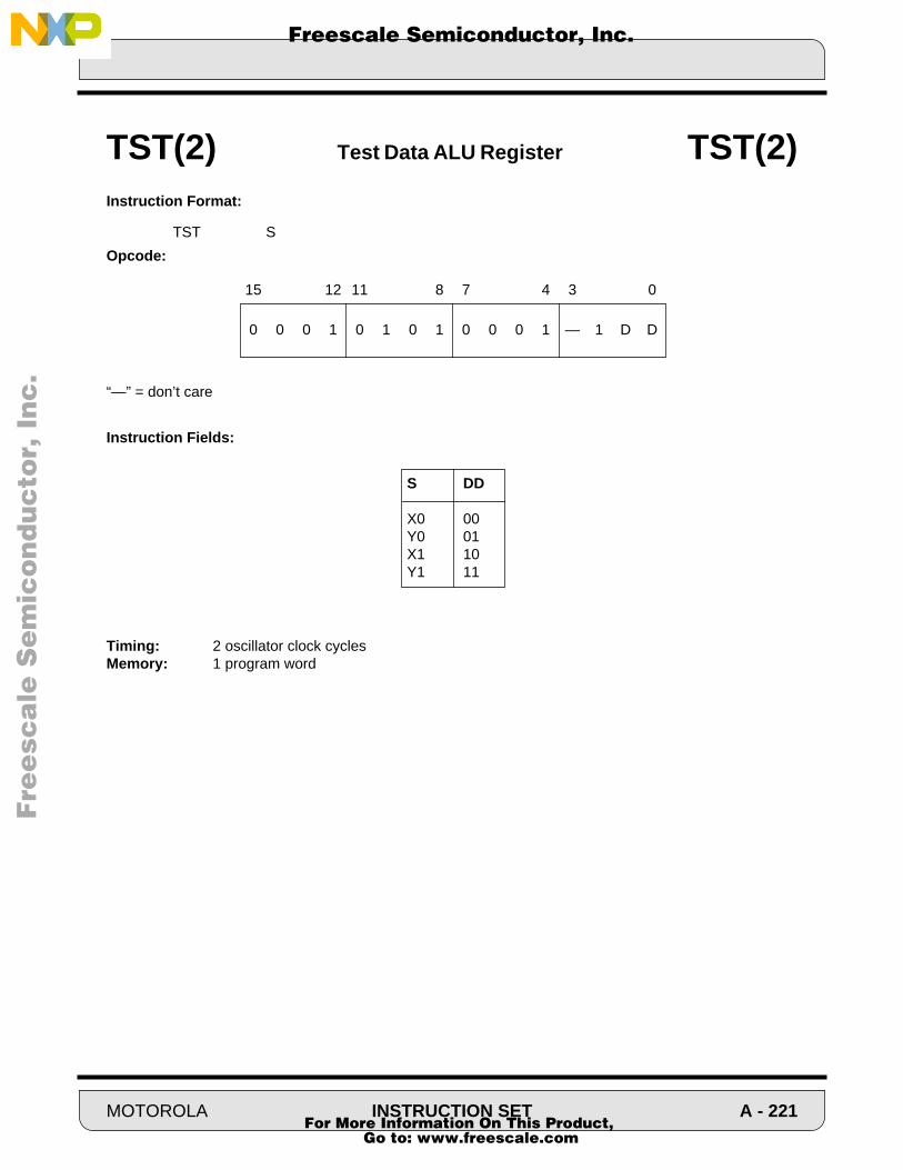
F
ree
sca
le S
em
ico
nd
uc
tor,
I
Freescale Semiconductor, Inc.n
c..
.
Instruction Format:
TST S
Opcode:
“—” = don’t care
Instruction Fields:
Timing: 2 oscillator clock cyclesMemory: 1 program word
TST(2) Test Data ALU Register TST(2)
0 0 0 1 0 1 0 1 0 0 0 1 — 1 D D
15 12 11 8 7 4 3 0
S DD
X0 00Y0 01X1 10Y1 11
MOTOROLA INSTRUCTION SET A - 221 For More Information On This Product,
Go to: www.freescale.com

F
ree
sca
le S
em
ico
nd
uc
tor,
I
Freescale Semiconductor, Inc.n
c..
.
Operation: Assembler Syntax:
Disable clocks to the processor core and enter the WAIT processing state. WAIT
Description: Enter the WAIT processing state. The internal clocks to the processor core and memoriesare gated off and all activity in the processor is suspended until an unmasked interrupt oc-curs. The clock oscillator and the internal I/O peripheral clocks remain active. When an un-masked interrupt or external (hardware) processor RESET occurs, the processor leavesthe WAIT state and begins exception processing of the unmasked interrupt or RESET con-dition. The WAIT state is a low-power standby mode.
Restrictions:
— A WAIT instruction cannot be used in a fast interrupt routine.— A WAIT instruction cannot be the last instruction in a DO loop (at LA).— A WAIT instruction cannot be repeated using the REP instruction.
Example:
:WAIT ;enter low power mode, wait for interrupt
:
Explanation of Example: The WAIT instruction suspends normal instruction execution and waits for anunmasked interrupt or external RESET to occur.
Condition Codes Affected:The condition codes are not affected by this instruction.
WAIT Wait for interrupt WAIT
A - 222 INSTRUCTION SET MOTOROLA For More Information On This Product,
Go to: www.freescale.com

F
ree
sca
le S
em
ico
nd
uc
tor,
I
Freescale Semiconductor, Inc.n
c..
.
Instruction Format:
WAIT
Opcode:
Instruction Fields: None
Timing: If an internal interrupt is pending during the execution of the WAIT instruction, the WAITinstruction takes a minimum of 32T cycles to execute. If no internal interrupt is pendingwhen the Wait instruction is executed, the period that the DSP is in the wait state is the pe-riod before the interrupt or reset causing the DSP to exit the wait state plus a minimum of28T cycles to a maximum of 31T cycles (see the Technical Data Sheet).
Memory: 1 program word
WAIT Wait for interrupt WAIT
0 0 0 0 0 0 0 0 0 0 0 0 1 0 1 1
15 12 11 8 7 4 3 0
MOTOROLA INSTRUCTION SET A - 223 For More Information On This Product,
Go to: www.freescale.com

F
ree
sca
le S
em
ico
nd
uc
tor,
I
Freescale Semiconductor, Inc.n
c..
.
Operation: Assembler Syntax:
0 → [bit 39-32] of D ZERO D (no parallel move)
Description: Zero Extend the destination accumulator from bit 32 to bit 39
Example:
ZERO A
Explanation of Example: Prior to execution, the 40-bit A accumulator contains the value $FF:6432:0000.Execution of the ZERO instruction clears the extension bits 32-39 and returns$00:6432:0000 in A.
Condition Codes Affected:
E — Always clearedU — Set according to the standard definition of the U bitN — Always cleared Z — Set if A or B result equals zeroV — Always cleared
ZERO Zero Extend Accumulator ZERO
A After Execution
00 3456 0000
A2 A1 A0
A Before Execution
12 3456 0000
A2 A1 A0
15 14 13 12 11 10 9 8 7 6 5 4 3 2 1 0
LF * * * S1 S0 I1 I0 S L E U N Z V C
CCRMR
A - 224 INSTRUCTION SET MOTOROLA For More Information On This Product,
Go to: www.freescale.com

F
ree
sca
le S
em
ico
nd
uc
tor,
I
Freescale Semiconductor, Inc.n
c..
.
Instruction Format:
ZERO D
Opcode:
Instruction Fields:
Timing: 2 oscillator clock cyclesMemory: 1 program word
ZERO Zero Extend Accumulator ZERO
0 0 0 1 0 1 0 1 0 1 0 1 F 0 0 0
15 12 11 8 7 4 3 0
D F
A 0B 1
MOTOROLA INSTRUCTION SET A - 225 For More Information On This Product,
Go to: www.freescale.com
INSTRUCTION TIMING
Fre
esc
ale
Se
mic
on
du
cto
r, I
Freescale Semiconductor, Inc.n
c..
.
A.6 INSTRUCTION TIMING
This section describes how one can calculate the 16-bit DSP instruction timing manuallyusing the tables provided in this section. Three complete examples are presented to illus-trate the “layered” nature of the tables. Alternatively, the user can obtain the number ofinstruction program words and the number of oscillator clock cycles required for a giveninstruction by using the 16-bit DSP simulator. This method of determining instruction tim-ing information is much faster and much simpler than using the aforementioned tables.
The number of words per instruction is dependent on the addressing mode and the typeof parallel data bus move operation specified. The symbols reference subsequent tablesto complete the instruction word count.
The number of oscillator clock cycles per instruction is dependent on many factors, includ-ing the number of words per instruction, the addressing mode, whether the instructionfetch pipe is full or not, the number of external bus accesses and the number of wait statesinserted in each external access. The symbols reference subsequent tables to completethe execution clock cycle count. The following is a list of these tables and their purpose.
• Table A-6 gives the number of instruction program words and the number of oscillator clock cycles for each instruction mnemonic.
• Table A-7 gives the number of additional (if any) instruction words and additional (if any) clock cycles for each type of parallel move operation.
• Table A-8 gives the number of additional (if any) clock cycles for each type of MOVEC operation.
• Table A-9 gives the number of additional (if any) clock cycles for each type of MOVEM operation.
• Table A-10 gives the number of additional (if any) clock cycles for each type of MOVEP operation.
• Table A-11 gives the number of additional (if any) clock cycles for each type of bit field manipulation (BFCHG, BFCLR, BFSET, BFTSTH, and BFTSTL) operation.
• Table A-12 gives the number of additional (if any) clock cycles for each type of branch/jump (Bcc, BRA, BSR, BScc, Jcc, JMP, JSR, and JScc) operation.
• Table A-13 gives the number of additional (if any) clock cycles for the RTI and RTS instructions.
• Table A-14 gives the number of additional (if any) instruction words and additional (if any) clock cycles for each effective addressing mode.
• Table A-15 gives the number of additional (if any) clock cycles for external data, external program, and external I/O memory accesses.
A - 226 INSTRUCTION SET MOTOROLA For More Information On This Product,
Go to: www.freescale.com
INSTRUCTION TIMING
Fre
esc
ale
Se
mic
on
du
cto
r, I
Freescale Semiconductor, Inc.n
c..
.
All tables are based on the following assumptions.
Assumptions:
1. All instruction cycles are counted in oscillator clock cycles.
2. The instruction fetch pipeline is full.
3. There is no contention for instruction fetches. Thus, external program instructionfetches are assumed not to have to contend with external data memory accesses.
4. There are no wait states for instruction fetches done sequentially (as for non-change-of-flow instructions), but they are taken into account for change-of-flow in-structions which flush the pipeline such as BRA/JMP, Bcc/Jcc, RTI, etc.
In order to better understand and use the aforementioned tables, three examples are pre-sented prior to the actual tables. These examples attempt to illustrate the “layered” natureof the tables.
Example 1: Arithmetic Instruction with 2 Parallel Reads
Problem: Calculate the number of 16-bit instruction program words and the number of oscillator clock cycles required for the instruction MACR X1,Y0,A X:(R0)+,Y0 X:(R3)+,X1
where Operating Mode Register (OMR) = $02 (normal expanded memory map),
Bus Control Register (BCR) = $20, R0 Address Register = $0052 (internal X memory), and R3 Address Register = $0923 (external X memory).
Solution: To determine the number of instruction program words and the number of oscillator clock cycles required for the given instruction, the user should per-form the following operations:
1. Look up the number of instruction program words and the number of oscillatorclock cycles required for the opcode-operand portion of the instruction in Table A-6.According to Table A-6, the MACR instruction will require 1 instruction programword and will execute in (2 + mv) oscillator clock cycles. The term “mv” representsthe additional (if any) instruction program words and the additional (if any) oscillatorclock cycles that may be required over and above those needed for the basicMACR instruction due to the parallel move portion of the instruction.
2. Evaluate the “mv” term using Table A-7. The parallel move portion of the MACR instruction consists of an XX MemoryRead. According to Table A-7, the parallel move portion of the instruction will re-quire mv = axx additional oscillator clock cycles. The term “axx” represents thenumber of additional (if any) oscillator clock cycles that are required to access twooperands in the X memory.
MOTOROLA INSTRUCTION SET A - 227 For More Information On This Product,
Go to: www.freescale.com

INSTRUCTION TIMING
Fre
esc
ale
Se
mic
on
du
cto
r, I
Freescale Semiconductor, Inc.n
c..
.
3. Evaluate the “axx” term using Table A-15. The parallel move portion of the MACR instruction consists of an XX MemoryRead. According to Table A-15, the term “axx” depends upon where the referencedX memory locations are located in the 16-bit DSP memory space. External X mem-ory accesses require additional oscillator clock cycles according to the number ofwait states programmed into the 16-bit DSP Bus Control Register (BCR). Thus, as-suming that the 16-bit Bus Control Register contains the value $20, external Xmemory accesses require wx = 1 wait state or additional oscillator clock cycle. Forthis example, the first X memory reference is assumed to be an internal referencewhile the second X memory reference is assumed to be an external reference.Thus, according to Table A-15, the XX memory reference in the parallel move por-tion of the MACR instruction will require axx = wx = 1 additional oscillator clock cy-cle.
4. Compute final results. Thus, based upon the assumptions given for Table A-6 and those listed in the prob-lem statement for Example 1, the instruction
MACR X1,Y0,A X:(R0)+,Y0 X:(R3)+,X1
will require 1instruction program word and will execute in (2 + mv) = (2 + axx) = (2 + wx) = (2 + 1) = 3 oscillator clock cycles.
Note that if a similar calculation were to be made for a MOVEC, MOVEM, MOVEP, or oneof the bit field manipulation (BFCHG, BFCLR, BFSET, or BFTST) instructions, the use ofTable A-7 would no longer be appropriate. For one of these cases, the user would referto Table A-8, Table A-9, Table A-10, or Table A-11, respectively.
Example 2: Jump Instruction
Problem: Calculate the number of 16-bit instruction program words and the number of oscillator clock cycles required for the instructionJLC R2
where Operating Mode Register (OMR) = $02 (normal expanded memory map), Bus Control Register (BCR) = $04, R2 Address Register= $2000 (external P memory)
Solution: To determine the number of instruction program words and the number of oscillator clock cycles required for the given instruction, the user should per-form the following operations:
1. Look up the number of instruction program words and the number of oscillator clockcycles required for the opcode-operand portion of the instruction in Table A-6. According to Table A-6, the Jcc instruction will require (1 + ea) instruction programwords and will execute in (4 + jx) oscillator clock cycles. The term “ea” representsthe number of additional (if any) instruction program words that are required for the
A - 228 INSTRUCTION SET MOTOROLA For More Information On This Product,
Go to: www.freescale.com

INSTRUCTION TIMING
))
Fre
esc
ale
Se
mic
on
du
cto
r, I
Freescale Semiconductor, Inc.n
c..
.
effective address of the Jcc instruction. The term “jx” represents the number of ad-ditional (if any) oscillator clock cycles required for a jump-type instruction.
2. Evaluate the “jx” term using Table A-12.According to Table A-12, the Jcc instruction will require jx = ea + (2 * ap) additionaloscillator clock cycles. The term “ea” represents the number of additional (if any) os-cillator clock cycles that are required for the effective addressing mode specified inthe Jcc instruction. The term “ap” represents the number of additional (if any) oscil-lator clock cycles that are required to access a P memory operand. Note that the “+(2 * ap)” term represents the two program memory instruction fetches executed atthe end of a one-word jump instruction to refill the instruction pipeline.
3. Evaluate the “ea” term using Table A-14.The JLC R2 instruction uses the “No update” effective addressing mode. Accordingto Table A-14, this operation will require ea = 0 additional instruction program wordsand ea = 0 additional oscillator clock cycles.
4. Evaluate the “ap” term using Table A-15.According to Table A-15, the term “ap” depends upon where the referenced P mem-ory location is located in the 16-bit DSP memory space. External memory accessesrequire additional oscillator clock cycles according to the number of wait states pro-grammed into the 16-bit DSP Bus Control Register (BCR). Thus, assuming that the16-bit Bus Control Register contains the value $04, external P memory accessesrequire wp = 4 wait states or additional oscillator clock cycles. For this example,the P memory reference is assumed to be an external reference. Thus, accordingto Table A-15, the Jcc instruction will use the value ap = wp = 4 oscillator clock cy-cles.
5. Compute final results.Thus, based upon the assumptions given for Table A-6 and those listed in the prob-lem statement for Example 2, the instruction
JLC R2
will require (1 + ea) = (1 + 0) = 1instruction program wordand will execute in (4 + jx) = (4 + ea + (2 * ap)) = (4 + ea + (2 * wp)) = (4 + 0 + (2 * 4= 12 oscillator clock cycles.
Example 3: RTI Instruction
Problem: Calculate the number of 16-bit instruction program words and the number of oscillator clock cycles required for the instruction RTI
where Operating Mode Register (OMR) = $02 (normal expanded memory map),Bus Control Register (BCR) = $41, andReturn Address (on the stack) = $0100 (internal P memory).
MOTOROLA INSTRUCTION SET A - 229 For More Information On This Product,
Go to: www.freescale.com
INSTRUCTION TIMING
Fre
esc
ale
Se
mic
on
du
cto
r, I
Freescale Semiconductor, Inc.n
c..
.
Solution: To determine the number of instruction program words and the number of oscillator clock cycles required for the given instruction, the user should per-form the following operations:
1. Look up the number of instruction program words and the number of oscillator clockcycles required for the opcode-operand portion of the instruction in Table A-6. According to Table A-6, the RTI instruction will require 1 instruction program wordand will execute in (4 + rx) oscillator clock cycles. The term “rx” represents the num-ber of additional (if any) oscillator clock cycles required for an RTI or RTS instruc-tion.
2. Evaluate the “rx” term using Table A-13. According to Table A-13, the RTI instruction will require rx = (2 * ap) additional os-cillator clock cycles. The term “ap” represents the number of additional (if any) os-cillator clock cycles that are required to access a P memory operand. Note that theterm “(2 * ap)” represents the two program memory instruction fetches executed atthe end of an RTI or RTS instruction to refill the instruction pipeline.
3. Evaluate the “ap” term using Table A-15. According to Table A-15, the term “ap” depends upon where the referenced P mem-ory location is located in the 16-bit DSP memory space. External memory accessesrequire additional oscillator clock cycles according to the number of wait states pro-grammed into the 16-bit DSP Bus Control Register (BCR). Thus, assuming that the16-bit Bus Control Register contains the value $0041, external P memory accessesrequire wp = 1 wait state or additional oscillator clock cycles. For this example, theP memory reference is assumed to be an internal reference. This means that thereturn address ($0100) pulled from the system stack by the RTI instruction is in in-ternal P memory. Thus, according to Table A-15, the RTI instruction will use the val-ue ap = 0 additional oscillator clock cycles.
4. Compute final results. Thus, based upon the assumptions given for Table A-6 and those listed in the prob-lem statement for Example 3, the instruction
RTI
will require one instruction program word and will execute in (4 + rx) = (4 + (2 * ap)) = (4 + (2 * 0)) = 4 oscillator clock cycles.
A - 230 INSTRUCTION SET MOTOROLA For More Information On This Product,
Go to: www.freescale.com

INSTRUCTION TIMING
Fre
esc
ale
Se
mic
on
du
cto
r, I
Freescale Semiconductor, Inc.n
c..
.
Table A-6 Instruction Timing Summary
Note 1: The STOP instruction disables the internal clock oscillator. After clock turn-on, an internal counter counts some 65,536 cycles before enabling the clock to the internal DSP circuits.
Mnemonic Instruction Osc. NotesProgram ClockWords Cycles
ABS 1 2+mvADC 1 2ADD 1 2+mvAND 1 2+mvANDI 1 2ASL 1 2+mvASL4 1 2ASR 1 2+mvASR4 1 2ASR16 1 2BFCHG 2 4+mvbBFCLR 2 4+mvbBFSET 2 4+mvbBFTSTH 2 4+mvbBFTSTL 2 4+mvbBcc 1+ea 4+jxBRA 1+ea 4+jxBRKcc 1 2/8 3BScc 1+ea 4+jxBSR 1+ea 4+jxCHKAAU 1 2CLR 1 2+mvCLR24 1 2+mvCMP 1 2+mvCMPM 1 2+mvDEBUG 1 4DEBUGcc 1 4DEC 1 2+mvDEC24 1 2+mvDIV 1 2DMAC 1 2DO 2 6/10+mv 4DOFOREVER 2 6ENDDO 1 2EOR 1 2+mvEXT 1 2ILLEGAL 1 8IMAC 1 2IMPY 1 2INC 1 2+mvINC24 1 2+mvJcc 1+ea 4+jxJMP 1+ea 4+jxJScc 1+ea 4+jx
Mnemonic Instruction Osc. NotesProgram ClockWords Cycles
JSR 1+ea 4+jxLEA 1 4LSL 1 2+mvLSR 1 2+mvMAC 1 2+mvMACR 1 2+mvMAC(uu,su) 1 2MOVE 1+ea 2+mvMOVE(C) 1+ea 2+mvcMOVE(I) 1 2MOVE(M) 1+ea 2+mvmMOVE(P) 1 4+mvpMOVE(S) 1 4+mvpMPY 1 2+mvMPYR 1 2+mvMPY(su,uu) 1 2NEG 1 2+mvNEGC 1 2NOP 1 2NORM 1 2NOT 1 2+mvOR 1 2+mvORI 1 2REP 1 4/6+mv 5REPcc 1 4/6 6RESET 1 4RND 1 2+mvROL 1 2+mvROR 1 2+mvRTI 1 4+rxRTS 1 4+rxSBC 1 2+mvSTOP 1 n/a 1SUB 1 2+mvSUBL 1 2+mvSWAP 1 2SWI 1 8Tcc 1 2TFR 1 2+mvTFR(2) 1 2TFR(3) 1 2+mvTST 1 2+mvTST(2) 1 2WAIT 1 n/a 2ZERO 1 2
MOTOROLA INSTRUCTION SET A - 231 For More Information On This Product,
Go to: www.freescale.com
INSTRUCTION TIMING
Fre
esc
ale
Se
mic
on
du
cto
r, I
Freescale Semiconductor, Inc.n
c..
.
Note 2: The WAIT instruction takes a minimum of 16 cycles to execute when an internal interrupt is pend-ing during the execution of the WAIT instruction.
Note 3: BRKcc executes in 8 clock cycles if cc is true. Otherwise it executes in 2 clock cycles.
Note 4: The DO instruction executes in 10 clock cycles if the DO argument is equal to zero. In that case, the loop is skipped. Otherwise it executes in 6 clock cycles.
Note 5: The REP instruction executes in 6 clock cycles if the argument is equal to zero. In that case, the repetition is skipped. Otherwise it executes in 4 clock cycles.
Note 6: REPcc executes in 6 clock cycles if cc is true on entry. Otherwise it executes in 4 clock cycles. When the condition becomes true, 4 additional clock cycles are necessary to exit the REP.
Table A-7 Parallel Data Move Timing
Table A-8 MOVEC Timing Summary
Table A-9 MOVEM Timing Summary
Note that the “ap” term present in Table A-9 represents the wait states spent when ac-cessing the program memory during DATA read or write operations and does not refer toinstruction fetches.
+ mv + mv Parallel Move operation Words Cycles Comments
No Parallel Data Move 0 0 I Immediate Short Data 0 0 R Register to Register 0 0 U Address Reg. Update 0 0 X: X Memory Move 0 axX: R X Memory and Register ea ea+axX: X: XX Memory Read 0 axx
+ mvc MOVEC Operation Cycles Comments
Immediate → Register 2 Register ↔ Register 0
X Memory ↔ Register ea + ax
+ mvm MOVEM Operation Cycles Comments
Register ↔ P Memory 4 + ea + ap
X Memory ↔ P Memory 4 + ea + ap
A - 232 INSTRUCTION SET MOTOROLA For More Information On This Product,
Go to: www.freescale.com

INSTRUCTION TIMING
Fre
esc
ale
Se
mic
on
du
cto
r, I
Freescale Semiconductor, Inc.n
c..
.
Table A-10 MOVEP Timing Summary
Table A-11 Bit Field Manipulation Timing Summary
where BFxxx = BFCHG, BFCLR, or BFSET and BFTSTx = BFTSTH or BFTSTL
Table A-12 Branch/Jump Instruction Timing Summary
where Bxxx = Bcc, BRA, BScc, and BSR Jxxx = Jcc, JMP, JScc, and JSR
The one word branch instructions using the 6-bit signed address, as well as all one-wordjump instructions, execute two program memory fetches to refill the pipeline which is rep-resented by the “+ (2 * ap)” term.
For all other branch instruction, another instruction cycle (two clock cycles) is necessaryto compute the new PC address from the relative address.
All two-word jumps execute three program memory fetches to refill the pipeline but oneof those fetches is sequential (the instruction word located at the jump instruction 2ndword address+1). If the jump instruction was fetched from program memory using waitstates, another “ap” should be added to account for that third fetch.
+ mvp MOVEP Operation Cycles Comments
Register ↔ Peripheral aio
X Memory ↔ Peripheral ea + ax + aio
+ mvb Bit Manipulation Operation Cycles Comments
BFxxx Peripheral 2 * aio BFxxx X Memory ea + (2 * ax)
BFTSTx Peripheral aio BFTSTx X Memory ea + ax
+ jx Branch/Jump Instruction Operation Cycles Comments
Bxxx eab + (2 * ap) Jxxx ea + (2 * ap)
MOTOROLA INSTRUCTION SET A - 233 For More Information On This Product,
Go to: www.freescale.com

INSTRUCTION TIMING
Fre
esc
ale
Se
mic
on
du
cto
r, I
Freescale Semiconductor, Inc.n
c..
.
Table A-13 RTI/RTS Timing Summary
The term “2 * ap” comes from the two instruction fetches done by the RTI/RTS instructionto refill the pipeline.
Table A-14 Addressing Mode Timing Summary
Operation + rx Cycles Comments
RTI 2 * ap RTS 2 * ap
+ ea + ea +eab Effective Addressing Mode Words Cycles Cycles
Address Register Indirect
No Update 0 0 2Postincrement by 1 0 0 —Postdecrement by 1 0 0 —
Post addition by Offset Nn 0 0 —Indexed by Offset Nn 0 2 —Predecrement by 1 0 2 —
Special
Immediate Data 1 2 —Absolute Address 1 2 2
Immediate Short Data 0 0 —Short Branch Address 0 — 0
Absolute Short Address 0 0 —I/O Short Address 0 0 —
Implicit 0 0 —Indexed by short displacement 1 2 —
Acc. Indirect Address 0 2 —
A - 234 INSTRUCTION SET MOTOROLA For More Information On This Product,
Go to: www.freescale.com
INSTRUCTION TIMING
Fre
esc
ale
Se
mic
on
du
cto
r, I
Freescale Semiconductor, Inc.n
c..
.
Table A-15 Memory Access Timing Summary
where wx = external X memory access wait states wp = external P memory access wait states
where wx and wp are programmable from 0-31 wait states in the Port A Bus Control Reg-ister (BCR).
Access X Mem P Mem I/O + ax + ap + aio + axxType Access Access Access Access Cycle Cycle Cycle X: Int – – 0 – – – X: Ext – – wx – – – P: – Int – – 0 – – P: – Ext – – wp – – IO: – – Int – – 0 – X:X: Int:Int – – – – – 0 X:X: Int:Ext – – – – – wx X:X: Ext:Ext – – – – – 2+2*wxX:X: I/O:I/O – – – – – 2 X:X: I/O:Int – – – – – 2 X:X: I/O:Ext – – – – – 2+2*wx
MOTOROLA INSTRUCTION SET A - 235 For More Information On This Product,
Go to: www.freescale.com

FUNCTIONAL SUMMARY
Fre
esc
ale
Se
mic
on
du
cto
r, I
Freescale Semiconductor, Inc.n
c..
.
A.7 FUNCTIONAL SUMMARY
Table A-16 Dual Read Instructions
DSP56100 Family
DATA ALU OPERATION
DOUBLE EFFECTIVE ADDRESS
DOUBLE DESTINATION
Oper. Reg. Read1 Read2 Dest1 Dest2
MOVE (Rn)+ (R3)+ F X0
MAC/RMPY/R
X1,Y1,FX1,Y0,FX0,Y1,FX0,Y0,F
(Rn)+Nn (R3)+ Y0 X0
(Rn)+ (R3)+N3 X1 X0
(Rn)+Nn (R3)+N3 Y1 X0
n=[0,2]
F = 0 → AF = 1 → B
X0 X1
ADDSUBTFR
X1,FX0,FY1,FY0,F
Y0 X1
F Y0
Y1 X1
ADD F,F
SUB F,F
TFR F,F
Table A-17 LMS Instruction
DSP56100 Family
DATA ALU OPERATION
DOUBLE TRANSFER
Oper. Reg. TRANSFER1 TRANSFER2
MACMPY
X0,X0,F F (Rn)+Nn X1 F
X1,X0,Fn=[0,2]F = 0 → AF = 1 → BF= Opposite accumulator
X0 F
A1,Y0,F Y1 F
B1,X0,F Y0 F
Y0,X1,F
Y1,X1,F
Y1,X0,F
Y0,X0,F
A - 236 INSTRUCTION SET MOTOROLA For More Information On This Product,
Go to: www.freescale.com

FUNCTIONAL SUMMARY
Fre
esc
ale
Se
mic
on
du
cto
r, I
Freescale Semiconductor, Inc.n
c..
.
Table A-18 Data ALU Instructions with One Parallel Operation
DSP56100 Family
DATA ALU OPERATION
PARALLEL MEMORYREAD or WRITE
Oper. Reg. Effective Address Dest/Source
MACMPY
+X0,X0,F+X1,X0,F+A1,Y0,F+B1,X0,F+Y0,X1,F+Y1,X1,F+Y1,X0,F+Y0,X0,F
(Rn)+(Rn)+Nn(F1)(R2+xx)
X1X0Y1Y0A0B0AB
ONE ADDRESS UPDATE
ADDSUBTFROR/ANDEORCMP/CMPM
X1,FX0,FY1,FY0,F
Effective Address
(Rn)-
(Rn)+Nn
PARALLEL REGISTER TRANSFER
Source Destination
X0 F
ADDSUB
X,FY,F
X1 F
Y0 F
MOVE Y1 F
SBC X,FY,F
A X0
A X1
CMP/CMPMSUBL, TFRADD, SUB
F,F B Y0
B Y1
RNDTSTABSINC/INC24DEC/DEC24CLR/CLR24NEGASL/ASRNOTROL/RORLSL/LSR
F F F
A0 X0
A0 X1
B0 Y0
B0 Y1
No Transfer
MOTOROLA INSTRUCTION SET A - 237 For More Information On This Product,
Go to: www.freescale.com
FUNCTIONAL SUMMARY
Fre
esc
ale
Se
mic
on
du
cto
r, I
Freescale Semiconductor, Inc.n
c..
.
Table A-19 Bit Field Manipulation Instructions
DSP56100 Family
OPERATION OPERAND COMMENTS
BFTSTH #iiii,BFTSTL #iiii,BFCHG #iiii,BFSET #iiii,BFCLR #iiii,
X:(Rn) n=[0,3]
X:<aa> First 32 words of Xmemory 5 bit address
X:<pp> Last 32 words of X memory 5 bit address
X1,X0,Y1,Y0,R0,R1,R2,R3,N0,N1,N2,N3M0,M1,M2,M3A2,B2,A1,B1,A0,B0,A,BSR,OMR,SP,SSH,SSL,LA,LC
Table A-20 Effective Address Update
DSP56100 Family
OPERATION SOURCE ADDRESS REGISTER
DESTINATION REGISTER
LEA (Rn)(Rn)+(Rn)-(Rn)+Nnn=[0,3]
R0,R1,R2,R3N0,N1,N2,N3
Table A-21 JUMP/BRANCH Instructions
DSP56100 Family
OPERATION OPERAND COMMENTS
JSRJMPJccJScc
(Rn) n=[0,3]
$xxxx 16-bit absolute address
A - 238 INSTRUCTION SET MOTOROLA For More Information On This Product,
Go to: www.freescale.com

FUNCTIONAL SUMMARY
Fre
esc
ale
Se
mic
on
du
cto
r, I
Freescale Semiconductor, Inc.n
c..
.
BSRBRABccBScc
(Rn) n=[0,3]
$xxxx 16-bit absolute address
JSR AA 8-bit absoluteaddress [0,256]
BRA aa 8-bit PC relativeaddress [-128,+127]
Bcc ee 6-bit PC relativeaddress [-32,+31]
Table A-22 REP and DO Instructions
DSP56100 Family
OPERATION OPERAND COMMENTS
REPDO
X:(Rn) n=[0,3]
#xx 8-bit immediate short data
X1,X0,Y1,Y0,R0,R1,R2,R3,N0,N1,N2,N3M0,M1,M2,M3A2,B2,A1,B1,A0,B0,A,BSR,OMR,SP,SSH,SSL,LA,LC
REPcc 16 conditions
DO FOREVER
Table A-21 JUMP/BRANCH Instructions
DSP56100 Family
OPERATION OPERAND COMMENTS
MOTOROLA INSTRUCTION SET A - 239 For More Information On This Product,
Go to: www.freescale.com

FUNCTIONAL SUMMARY
Fre
esc
ale
Se
mic
on
du
cto
r, I
Freescale Semiconductor, Inc.n
c..
.
Table A-23 Short Immediate Move Instructions
DSP56100 Family
OPERATION DESTINATION COMMENTS
MOVE(I) #xx, X1X0Y1Y0
immediate short 8 bit signed data(data is put in the LSByte)
Table A-24 MOVE Program and Control Instructions
DSP56100 Family
OPERATION Source/Dest. Dest./Source COMMENTS
MOVE(M) P:(Rn)P:(Rn)+P:(Rn)-P:(Rn)+NnP:(R2+xx)
A, A0, B, B0X0, X1, Y0, Y1
MOVE(M) X:(Rn)+X:(Rn)+Nn
P:(Rn)+P:(Rn)+Nn
MOVE(C) X:(Rn)X:(Rn)+X:(Rn)-X:(Rn)+NnX:(Rn+Nn)X:-(Rn)X:#xxxx#xxxxX:(A1)X:(B1)X:(R2+xx)
All registers X:#xxxx: Long 16-bitabsolute address
#xxxx: Long 16-bitimmediatedata
MOVE(C) All registers All registers
A - 240 INSTRUCTION SET MOTOROLA For More Information On This Product,
Go to: www.freescale.com

FUNCTIONAL SUMMARY
Fre
esc
ale
Se
mic
on
du
cto
r, I
Freescale Semiconductor, Inc.n
c..
.
Table A-25 MOVE Absolute Short andMOVE Peripheral Instructions
DSP56100 Family
OPERATION Source/Dest. Dest./Source COMMENTS
MOVE(S) X:<aa> A, B,X0, Y0
First 32 word of X memory5 bit address
MOVE(P) X:<pp> A, B,X0, Y0
Last 32 word of X memory5 bit address
X:(Rn)+X:(Rn)+Nn
Table A-26 Transfer with Parallel MOVE Instruction
DSP56100 Family
OPERATION REGISTER TRANSFER PARALLEL MOVE
Source Destination Source/Dest. Dest./Source
TFR(3) AB
X0, X1,Y0, Y1
X:(Rn)+X:(Rn)+Nn
X0,X1,Y0,Y1,A0, B0, A, B
Table A-27 Register Transfer without Parallel MOVE Instruction
DSP56100 Family
OPERATION SOURCE DESTINATION
TFR(2) AB
XY
Table A-28 Register Transfer Conditional MOVE Instruction
DSP56100 Family
OPERATION Data ALU Address Register
Tcc A, FB, FY0, FX0, F
R0,R0
R0,Rm
MOTOROLA INSTRUCTION SET A - 241 For More Information On This Product,
Go to: www.freescale.com
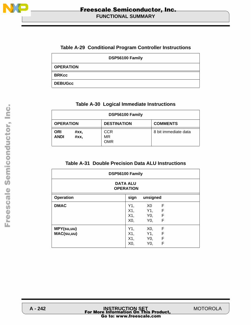
FUNCTIONAL SUMMARY
Fre
esc
ale
Se
mic
on
du
cto
r, I
Freescale Semiconductor, Inc.n
c..
.
Table A-29 Conditional Program Controller Instructions
DSP56100 Family
OPERATION
BRKcc
DEBUGcc
Table A-30 Logical Immediate Instructions
DSP56100 Family
OPERATION DESTINATION COMMENTS
ORI #xx,ANDI #xx,
CCRMROMR
8 bit immediate data
Table A-31 Double Precision Data ALU Instructions
DSP56100 Family
DATA ALU OPERATION
Operation sign unsigned
DMAC Y1, X0 FX1, Y1, FX1, Y0, FX0, Y0, F
MPY(su,uu)MAC(su,uu)
Y1, X0, FX1, Y1, FX1, Y0, FX0, Y0, F
A - 242 INSTRUCTION SET MOTOROLA For More Information On This Product,
Go to: www.freescale.com
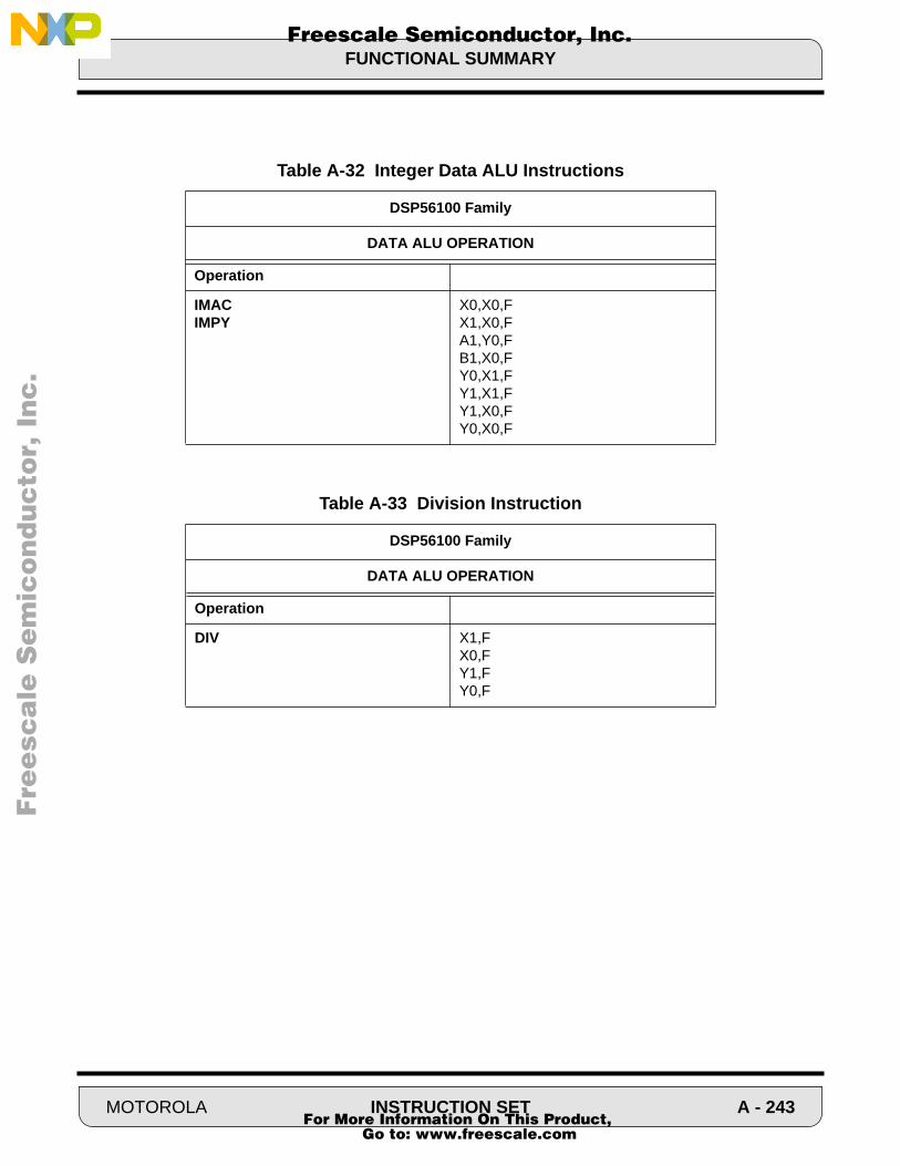
FUNCTIONAL SUMMARY
Fre
esc
ale
Se
mic
on
du
cto
r, I
Freescale Semiconductor, Inc.n
c..
.
Table A-32 Integer Data ALU Instructions
DSP56100 Family
DATA ALU OPERATION
Operation
IMACIMPY
X0,X0,FX1,X0,FA1,Y0,FB1,X0,FY0,X1,FY1,X1,FY1,X0,FY0,X0,F
Table A-33 Division Instruction
DSP56100 Family
DATA ALU OPERATION
Operation
DIV X1,FX0,FY1,FY0,F
MOTOROLA INSTRUCTION SET A - 243 For More Information On This Product,
Go to: www.freescale.com
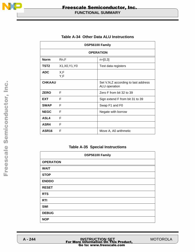
FUNCTIONAL SUMMARY
Fre
esc
ale
Se
mic
on
du
cto
r, I
Freescale Semiconductor, Inc.n
c..
.
Table A-34 Other Data ALU Instructions
DSP56100 Family
OPERATION
Norm Rn,F n=[0,3]
TST2 X1,X0,Y1,Y0 Test data registers
ADC X,FY,F
CHKAAU Set V,N,Z according to last address ALU operation
ZERO F Zero F from bit 32 to 39
EXT F Sign extend F from bit 31 to 39
SWAP F Swap F1 and F0
NEGC F Negate with borrow
ASL4 F
ASR4 F
ASR16 F Move A, A0 arithmetic
Table A-35 Special Instructions
DSP56100 Family
OPERATION
WAIT
STOP
ENDDO
RESET
RTS
RTI
SWI
DEBUG
NOP
A - 244 INSTRUCTION SET MOTOROLA For More Information On This Product,
Go to: www.freescale.com
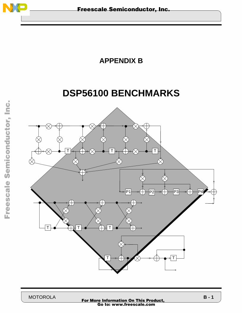
Fre
esc
ale
Se
mic
on
du
cto
r, I
Freescale Semiconductor, Inc.n
c..
.
APPENDIX B
DSP56100 BENCHMARKS
T T T
T T
P1 P3P2 P4
T T T
MOTOROLA B - 1 For More Information On This Product,
Go to: www.freescale.com

SECTION CONTENTS
Fre
esc
ale
Se
mic
on
du
cto
r, I
Freescale Semiconductor, Inc.n
c..
.
B.1 INTRODUCTION . . . . . . . . . . . . . . . . . . . . . . . . . . . . . . . . . . . . . . . . B-3B.2 FIRST SET OF BENCHMARKS . . . . . . . . . . . . . . . . . . . . . . . . . . . . . B-5B.2.1 Real Multiply . . . . . . . . . . . . . . . . . . . . . . . . . . . . . . . . . . . . . . . . . . . . B-5B.2.2 N Real Multiplies . . . . . . . . . . . . . . . . . . . . . . . . . . . . . . . . . . . . . . . . . B-5B.2.3 Real Update . . . . . . . . . . . . . . . . . . . . . . . . . . . . . . . . . . . . . . . . . . . . B-5B.2.4 N Real Updates . . . . . . . . . . . . . . . . . . . . . . . . . . . . . . . . . . . . . . . . . . B-6B.2.5 Real Correlation Or Convolution (FIR Filter) . . . . . . . . . . . . . . . . . . . . B-6B.2.6 Real * Complex Correlation Or Convolution (FIR Filter) . . . . . . . . . . . B-7B.2.7 Complex Multiply . . . . . . . . . . . . . . . . . . . . . . . . . . . . . . . . . . . . . . . . . B-7B.2.8 N Complex Multiplies . . . . . . . . . . . . . . . . . . . . . . . . . . . . . . . . . . . . . B-8B.2.9 Complex Update . . . . . . . . . . . . . . . . . . . . . . . . . . . . . . . . . . . . . . . . . B-8B.2.10 N Complex Updates . . . . . . . . . . . . . . . . . . . . . . . . . . . . . . . . . . . . . . B-9B.2.11 Complex Correlation Or Convolution (Complex FIR) . . . . . . . . . . . . . B-9B.2.12 Nth Order Power Series (Real) . . . . . . . . . . . . . . . . . . . . . . . . . . . . . . B-10B.2.13 2nd Order Real Biquad IIR Filter . . . . . . . . . . . . . . . . . . . . . . . . . . . . . B-10B.2.14 N Cascaded Real Biquad IIR Filters . . . . . . . . . . . . . . . . . . . . . . . . . . B-11B.2.15 N Radix 2 FFT Butterflies . . . . . . . . . . . . . . . . . . . . . . . . . . . . . . . . . . B-13B.2.16 LMS Adaptive Filter . . . . . . . . . . . . . . . . . . . . . . . . . . . . . . . . . . . . . . . B-14B.2.17 FIR Lattice Filter . . . . . . . . . . . . . . . . . . . . . . . . . . . . . . . . . . . . . . . . . B-24B.2.18 All Pole IIR Lattice Filter . . . . . . . . . . . . . . . . . . . . . . . . . . . . . . . . . . . B-25B.2.19 General Lattice Filter . . . . . . . . . . . . . . . . . . . . . . . . . . . . . . . . . . . . . . B-26B.2.20 Normalized Lattice Filter . . . . . . . . . . . . . . . . . . . . . . . . . . . . . . . . . . . B-27B.2.21 [1x3][3x3] Matrix Multiply . . . . . . . . . . . . . . . . . . . . . . . . . . . . . . . . . . B-28B.2.22 [NxN][NxN] Matrix Multiply . . . . . . . . . . . . . . . . . . . . . . . . . . . . . . . . . B-29B.2.23 N Point 3x3 2-D FIR Convolution . . . . . . . . . . . . . . . . . . . . . . . . . . . . B-30B.2.24 Signed 16 Bit Result Divide . . . . . . . . . . . . . . . . . . . . . . . . . . . . . . . . B-32B.2.25 Signed Integer Divide . . . . . . . . . . . . . . . . . . . . . . . . . . . . . . . . . . . . . B-33B.2.26 Multiply 32-bit Fractions . . . . . . . . . . . . . . . . . . . . . . . . . . . . . . . . . . . B-34B.3 SECOND SET OF BENCHMARKS . . . . . . . . . . . . . . . . . . . . . . . . . . B-35B.3.1 Sine Wave Generation Using Double Integration Technique . . . . . . . B-35B.3.2 Sine Wave Generation Using Second Order Oscillator . . . . . . . . . . . B-36B.3.3 IIR Filter Using Cascaded Transpose BIQUAD Cell . . . . . . . . . . . . . . B-37B.3.4 Find the Index of a Maximum Value in an Array . . . . . . . . . . . . . . . . . B-39B.3.5 Proportional Integrator Differentiator (PID) Algorithm . . . . . . . . . . . . . B-40B.3.6 Reed Solomon Main Loop . . . . . . . . . . . . . . . . . . . . . . . . . . . . . . . . . B-41B.3.7 N Double Precision Real Multiplies . . . . . . . . . . . . . . . . . . . . . . . . . . . B-42B.3.8 Double Precision Autocorrelation . . . . . . . . . . . . . . . . . . . . . . . . . . . . B-42
B - 2 MOTOROLA For More Information On This Product,
Go to: www.freescale.com

INTRODUCTION
Fre
esc
ale
Se
mic
on
du
cto
r, I
Freescale Semiconductor, Inc.n
c..
.
B.1 INTRODUCTION
Appendix B consists of a set of DSP Benchmarks intended to highlight the DSP56100 family performancein various applications, show examples of programming techniques, and provide code fragments for userapplication programs. Additional code will be put on the Dr. Bub Electronic Bulletin Board System as it be-comes available. The following table lists these Benchmark programs and provides an overview of the pro-gram’s performance.
The assembly language source is organized into 5 columns as shown below.
Label Opcode Operands Data Bus Data Bus Comment FIR MAC X1,X0,A X:(R0)+,X1 X:(R3)+,X0 ;Do each tap
The Label column is used for program entry points and end of loop indication. The Opcode column indicatesthe Data ALU, Address ALU or Program Controller operation to be performed. The Operands column spec-ifies the operands to be used by the opcode. The Data Bus specifies an optional data transfer over the DataBus and the addressing mode to be used. The Comment column is used for documentation purposes anddoes not affect the assembled code. The Opcode column must always be included in the source code. Foreach benchmark, the number of program words and instruction cycles are given.
The following equates are used in the benchmark programs.
page 132 k equ 0
opt cc;define sectionAD EQU 0BD EQU $100bd EQU $100C EQU $200c EQU $200D EQU $300N EQU 100AR EQU $300AI EQU $400OUTPUT EQU $500output EQU $FFF1INPUT EQU $501input EQU $FFF1W EQU 0w EQU 0H EQU 0XM EQU 0state equ 0ntaps equ $10
n equ 32p equ 10mask equ 10image equ $40dividend equ .25divisor equ .5paddr equ 0qaddr equ 4w1 equ 0w2 equ 10s equ 0tablebase equ 0lpc equ 8frame equ 0cor equ $100shift equ $80 ;shift constanttable equ $180 ;base address of a-law table
org p:$40
MOTOROLA B - 3 For More Information On This Product,
Go to: www.freescale.com
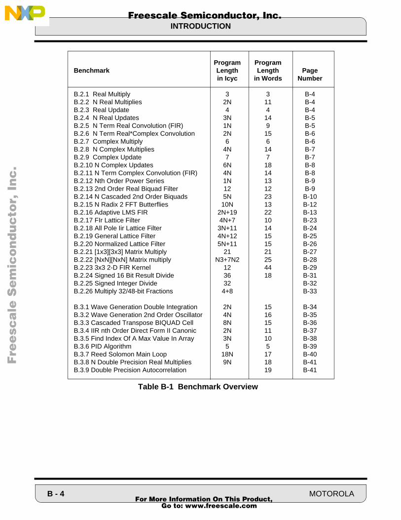
INTRODUCTION
Fre
esc
ale
Se
mic
on
du
cto
r, I
Freescale Semiconductor, Inc.n
c..
.
Program ProgramBenchmark Length Length Page
in Icyc in Words Number
B.2.1 Real Multiply 3 3 B-4B.2.2 N Real Multiplies 2N 11 B-4B.2.3 Real Update 4 4 B-4B.2.4 N Real Updates 3N 14 B-5B.2.5 N Term Real Convolution (FIR) 1N 9 B-5B.2.6 N Term Real*Complex Convolution 2N 15 B-6B.2.7 Complex Multiply 6 6 B-6B.2.8 N Complex Multiplies 4N 14 B-7B.2.9 Complex Update 7 7 B-7B.2.10 N Complex Updates 6N 18 B-8B.2.11 N Term Complex Convolution (FIR) 4N 14 B-8B.2.12 Nth Order Power Series 1N 13 B-9B.2.13 2nd Order Real Biquad Filter 12 12 B-9B.2.14 N Cascaded 2nd Order Biquads 5N 23 B-10B.2.15 N Radix 2 FFT Butterflies 10N 13 B-12B.2.16 Adaptive LMS FIR 2N+19 22 B-13B.2.17 FIr Lattice Filter 4N+7 10 B-23B.2.18 All Pole Iir Lattice Filter 3N+11 14 B-24B.2.19 General Lattice Filter 4N+12 15 B-25B.2.20 Normalized Lattice Filter 5N+11 15 B-26B.2.21 [1x3][3x3] Matrix Multiply 21 21 B-27B.2.22 [NxN][NxN] Matrix multiply N3+7N2 25 B-28B.2.23 3x3 2-D FIR Kernel 12 44 B-29B.2.24 Signed 16 Bit Result Divide 36 18 B-31B.2.25 Signed Integer Divide 32 B-32B.2.26 Multiply 32/48-bit Fractions 4+8 B-33
B.3.1 Wave Generation Double Integration 2N 15 B-34B.3.2 Wave Generation 2nd Order Oscillator 4N 16 B-35B.3.3 Cascaded Transpose BIQUAD Cell 8N 15 B-36B.3.4 IIR nth Order Direct Form II Canonic 2N 11 B-37B.3.5 Find Index Of A Max Value In Array 3N 10 B-38B.3.6 PID Algorithm 5 5 B-39B.3.7 Reed Solomon Main Loop 18N 17 B-40B.3.8 N Double Precision Real Multiplies 9N 18 B-41B.3.9 Double Precision Autocorrelation 19 B-41
Table B-1 Benchmark Overview
B - 4 MOTOROLA For More Information On This Product,
Go to: www.freescale.com
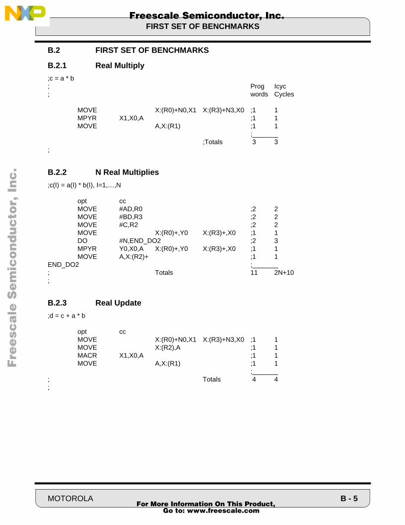
FIRST SET OF BENCHMARKS
Fre
esc
ale
Se
mic
on
du
cto
r, I
Freescale Semiconductor, Inc.n
c..
.
B.2 FIRST SET OF BENCHMARKS
B.2.1 Real Multiply
;c = a * b; Prog Icyc; words Cycles
MOVE X:(R0)+N0,X1 X:(R3)+N3,X0 ;1 1MPYR X1,X0,A ;1 1MOVE A,X:(R1) ;1 1
;_______;Totals 3 3
;
B.2.2 N Real Multiplies
;c(I) = a(I) * b(I), I=1,…,N
opt ccMOVE #AD,R0 ;2 2MOVE #BD,R3 ;2 2MOVE #C,R2 ;2 2MOVE X:(R0)+,Y0 X:(R3)+,X0 ;1 1DO #N,END_DO2 ;2 3
MPYR Y0,X0,A X:(R0)+,Y0 X:(R3)+,X0 ;1 1MOVE A,X:(R2)+ ;1 1
END_DO2 ;_______; Totals 11 2N+10;
B.2.3 Real Update
;d = c + a * b
opt ccMOVE X:(R0)+N0,X1 X:(R3)+N3,X0 ;1 1MOVE X:(R2),A ;1 1MACR X1,X0,A ;1 1MOVE A,X:(R1) ;1 1
;_______; Totals 4 4;
MOTOROLA B - 5 For More Information On This Product,
Go to: www.freescale.com
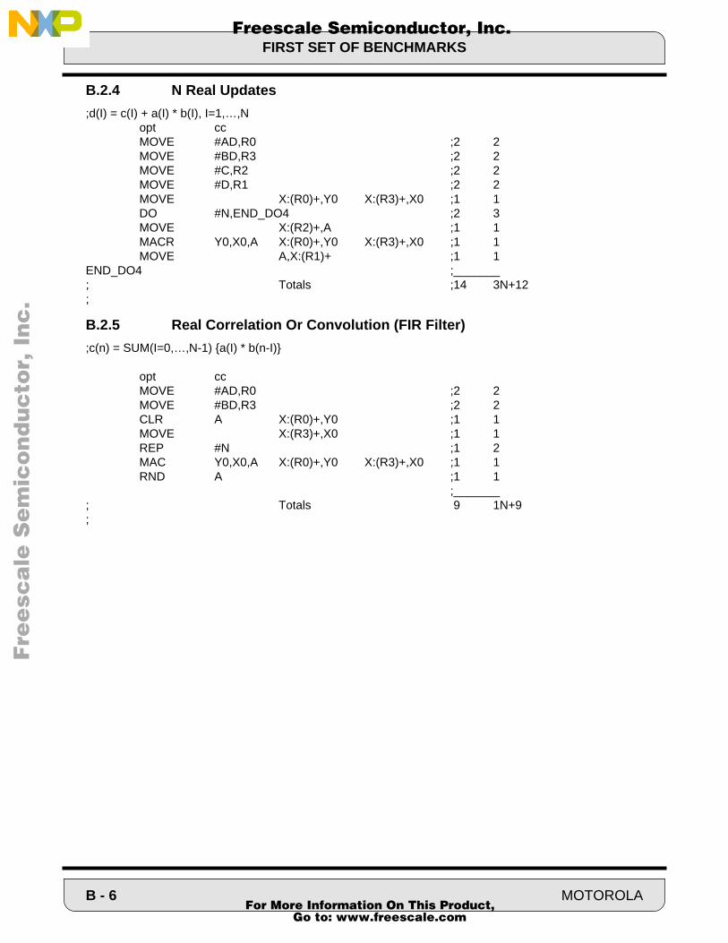
FIRST SET OF BENCHMARKS
Fre
esc
ale
Se
mic
on
du
cto
r, I
Freescale Semiconductor, Inc.n
c..
.
B.2.4 N Real Updates
;d(I) = c(I) + a(I) * b(I), I=1,…,Nopt ccMOVE #AD,R0 ;2 2MOVE #BD,R3 ;2 2MOVE #C,R2 ;2 2MOVE #D,R1 ;2 2MOVE X:(R0)+,Y0 X:(R3)+,X0 ;1 1DO #N,END_DO4 ;2 3MOVE X:(R2)+,A ;1 1MACR Y0,X0,A X:(R0)+,Y0 X:(R3)+,X0 ;1 1MOVE A,X:(R1)+ ;1 1
END_DO4 ;_______; Totals ;14 3N+12;
B.2.5 Real Correlation Or Convolution (FIR Filter)
;c(n) = SUM(I=0,…,N-1) a(I) * b(n-I)
opt ccMOVE #AD,R0 ;2 2MOVE #BD,R3 ;2 2CLR A X:(R0)+,Y0 ;1 1MOVE X:(R3)+,X0 ;1 1REP #N ;1 2MAC Y0,X0,A X:(R0)+,Y0 X:(R3)+,X0 ;1 1RND A ;1 1
;_______; Totals 9 1N+9;
B - 6 MOTOROLA For More Information On This Product,
Go to: www.freescale.com

FIRST SET OF BENCHMARKS
Fre
esc
ale
Se
mic
on
du
cto
r, I
Freescale Semiconductor, Inc.n
c..
.
B.2.6 Real * Complex Correlation Or Convolution (FIR Filter)
;cr(n) + jci(n) = SUM(I=0,…,N-1) (ar(I) + jai(I)) * b(n-I) ;cr(n) = SUM(I=0,…,N-1) ar(I) * b(n-I);ci(n) = SUM(I=0,…,N-1) ai(I) * b(n-I)
opt ccMOVE #AR,R0 ;2 2MOVE #AI,R1 ;2 2MOVE #BD,R3 ;2 2CLR A X:(R0)+,X1 ;1 1CLR B X:(R1)+,Y1 ;1 1MOVE X:(R3)+,X0 ;1 1DO #N,END_DO6 ;2 3MAC X0,X1,A X:(R0)+,X1 ;1 1MAC X0,Y1,B X:(R1)+,Y1 X:(R3)+,X0 ;1 1
END_DO6RND A ;1 1RND B ;1 1
; _______; Totals 15 2N+14;
B.2.7 Complex Multiply
opt ccMOVE X:(R0)+,Y1 X:(R3)+,X1 ;1 1 ar brMPY Y1,X1,A X:(R0)+,Y0 X:(R3)+,X0 ;1 1 ar*br, ai, biMACR -Y0,X0,A ;1 1 ar*br-ai*biMPY Y1,X0,B A,X:(R2)+ ;1 1 ar*biMACR Y1,X0,B ;1 1 ar*bi+ai*brMOVE B,X:(R2)+ ;1 1
; ________; Totals 6 6;
X memoryarai
brbi
crci
’
r0
r3
r2
cr + jci = (ar + jai)*(br + jbi)cr = ar*br - ai*bici = ar*bi + ai*br
Y1 = ar X1 = brY0 = ai X0 = bi
MOTOROLA B - 7 For More Information On This Product,
Go to: www.freescale.com

FIRST SET OF BENCHMARKS
Fre
esc
ale
Se
mic
on
du
cto
r, I
Freescale Semiconductor, Inc.n
c..
.
B.2.8 N Complex Multiplies
; cr(I) + jci(I) = (ar(I) + jai(I)) * (br(I) + jbi(I)), I=1,…,N ; cr(I) = ar(I) * br(I) - ai(I) * bi(I) Y1=ar X1=br; ci(I) = ar(I) * bi(I) + ai(I) * br(I) Y0=ai X0=bi
opt ccMOVE #AD,R0 ;2 2MOVE #C-1,R2 ;2 2MOVE #BD,R3 ;2 2MOVE X:(R2),B ; dummy move!MOVE X:(R0)+,Y1 X:(R3)+,X1 ;1 1 ar;br DO #N,END_DO8 ;2 3MPY Y1,X1,A X:(R0)+,Y0 X:(R3)+,X0 ;1 1 ar*br, ai, biMACR -Y0,X0,A B,X:(R2)+ ;1 1 ar*br-ai*biMPY Y0,X1,B A,X:(R2)+ ;1 1 ai*brMACR Y1,X0,B X:(R0)+,Y1 X:(R3)+,X1 ;1 1 ar*bi+ai*br, ar
END_DO8 MOVE B,X:(R2)+ ;1 1
; _______; Totals: 14 4N+11;
B.2.9 Complex Update
opt ccMOVE X:(R2)+,A ;1 1 crMOVE X:(R0)+,Y1 X:(R3)+,X1 ;1 1MAC Y1,X1,A X:(R0)+,Y0 X:(R3)+,X0 ;1 1 cr+ar*br,ai,biMACR -Y0,X0,A X:(R2)+,B ;1 1 cr+ar*br ai*biMAC Y1,X0,B A,X:(R1)+ ;1 1 ci+ar*biMACR Y0,X1,B ;1 1 ci+ar*bi+ai*brMOVE B,X:(R1)+ ;1 1
; ________; Totals 7 7;
X memoryarai
brbi
crci
drdi
r0
r3
r1
dr + jdi = cr + jci + (ar + jai)*(br + jbi)dr = cr + ar*br - ai*bidi = ci + ar*bi + ai*br
Y1 = ar X1 = brY0 = ai X0 = bi r2
B - 8 MOTOROLA For More Information On This Product,
Go to: www.freescale.com

FIRST SET OF BENCHMARKS
Fre
esc
ale
Se
mic
on
du
cto
r, I
Freescale Semiconductor, Inc.n
c..
.
B.2.10 N Complex Updates
opt ccMOVE #AD,R0 ;2 2MOVE #BD,R3 ;2 2MOVE #D-1,R1 ;2 2MOVE #C,R2 ;2 2MOVE X:(R1),B ; dummy in BMOVE X:(R0)+,Y1 ;1 1 arDO #N,END_DOA ;2 3MOVE X:(R2)+,A X:(R3)+,X0 ;1 1 cr,brMAC Y1,X0,A X:(R0)+,Y0 X:(R3)+,X1 ;1 1 cr+ar*br, ai, biMACR -Y0,X1,A B,X:(R1)+ ;1 1 cr+ar*br ai*biMOVE X:(R2)+,B ;1 1 ciMPY Y1,X1,B A,X:(R1)+ ;1 1 ci+ar*bi, drMACR Y0,X0,B X:(R0)+,Y1 ;1 1 ci+ar*bi+ai*br
END_DOAMOVE B,X:(R1)+ ;1 1
; _______; Totals 18 6N+13;
B.2.11 Complex Correlation Or Convolution (Complex FIR)
; cr(n) + jci(n) = SUM(I=0,…,N-1) (ar(I) + jai(I)) * (br(n-I) + jbi(n-I)); cr(n) = SUM(I=0,…,N-1) ar(I) * br(n-I) - ai(I) * bi(n-I) Y1=ar X1=br; ci(n) = SUM(I=0,…,N-1) ar(I) * bi(n-I) + ai(I) * br(n-I) Y0=ai X0=bi
opt ccMOVE #AD,R0 ;2 2MOVE #BD,R3 ;2 2CLR A X:(R0)+,Y1 ;1 1 arCLR B X:(R3)+,X1 ;1 1 brDO #N,END_DOB ;2 3MAC Y1,X1,A X:(R0)+,Y0 X:(R3)+,X0 ;1 1 ar*br, ai, biMAC Y1,X0,B ;1 1 ar*biMAC Y0,X1,B X:(R0)+,Y1 X:(R3)+,X1 ;1 1 ar*bi+ai*br, arMAC -Y0,X0,A ;1 1 ar*br-ai*bi
END_DOBRND A ;1 1RND B ;1 1
; _______; Totals 14 4N+11;
MOTOROLA B - 9 For More Information On This Product,
Go to: www.freescale.com

FIRST SET OF BENCHMARKS
Fre
esc
ale
Se
mic
on
du
cto
r, I
Freescale Semiconductor, Inc.n
c..
.
B.2.12 Nth Order Power Series (Real)
; c = SUM(I=0,…,N) a(I) * b**I = [[[a(n) *b+a(n-1)] *b+a(n-2)]*b+a(n-3)]…
opt ccMOVE #BD,R1 ;2 2MOVE #AD,R0 ;2 2MOVE X:(R1),Y0 ;1 1 bMOVE Y0,X0 ;1 1MOVE X:(R0)+,A ;1 1 a(n)MOVE X:(R0)+,B ;1 1 a(n-1)DO #N/2,END_DOC ;2 3MAC A1,Y0,B X:(R0)+,A ;1 1 a(n-2)MAC B1,X0,A X:(R0)+,B ;1 1 a(0)+a(1)*b
END_DOCRND A ;1 1
;_______; Totals 13 1N+12;
B.2.13 2nd Order Real Biquad IIR Filter
; w(n)/2 = x(n)/2 - (a1/2) * w(n-1) - (a2/2) * w(n-2); y(n)/2 = w(n)/2 + (b1/2) * w(n-1) + (b2/2) * w(n-2)
; DHigh Memory Order - w(n-2), w(n-1); DLow Memory Order - (a2/2), (a1/2), (b2/2), (b1/2)
; this version uses two pointersopt ccMOVE #-1,N0 ;2 2ORI #$08,MR ;1 1RND A X:(R3)+,X1 ;1 1 X1=a2/2MOVE X:(R0)+,X0 ;1 1 X0=wn-2MAC Y1,X0,A X:(R0)+N0,Y1 X:(R3)+,X1 ;1 1 y1=wn-1MAC Y1,X1,A X1,X:(R0)+ ;1 1 a=wnMOVE X:(R3)+,X1 ;1 1 x1=b2/2MAC X1,X0,A A,X:(R0)+ ;1 1MOVE X:(R3)+,X1 ;1 1 X1=b1/2MACR Y1,X1,A ;1 1
MOVE A,X:<<output ;1 1; _______; Totals 12 12;
B - 10 MOTOROLA For More Information On This Product,
Go to: www.freescale.com

FIRST SET OF BENCHMARKS
Fre
esc
ale
Se
mic
on
du
cto
r, I
Freescale Semiconductor, Inc.n
c..
.
B.2.14 N Cascaded Real Biquad IIR Filters
; w(n)/2 = x(n)/2 - (a1/2) * w(n-1) - (a2/2) * w(n-2); y(n)/2 = w(n)/2 + (b1/2) * w(n-1) + (b2/2) * w(n-2)
; D High Memory Order - w(n-2)1,w(n-1)1,w(n-2)2,w(n-1)2,…; D Low Memory Order - (a2/2)1,(a1/2)1,(b2/2)1,(b1/2)1,(a2/2)2,…
; this version uses two pointers
opt ccORI #$08,MR ;1 1MOVE #W,R0 ;2 2MOVE #C,R3 ;2 2MOVE #-1,N0 ;2 2movep x:<<input,A ;1 5RND A X:(R3)+,X1 ;1 1 X1=a2/2MOVE X:(R0)+,Y0 ;1 1 Y0=wn-2DO #N,END_DOE ;2 3MAC Y0,X1,A X:(R0)+N0,Y1 X:(R3)+,X1 ;1 1 y1=wn-1MACR Y1,X1,A Y1,(R0)+ ;1 1MOVE X:(R3)+,X1 ;1 1 X1= b2/2MAC Y0,X1,A A,X:(R0)+ ;1 1MOVE X:(R3)+,X1 ;1 1 X1=b1/2MAC Y1,X1,A X:(R0)+,Y0 X:(R3)+,X1 ;1 1
END_DOE ;_______; Totals 18 6N+14;
MOTOROLA B - 11 For More Information On This Product,
Go to: www.freescale.com

FIRST SET OF BENCHMARKS
Fre
esc
ale
Se
mic
on
du
cto
r, I
Freescale Semiconductor, Inc.n
c..
.
;this version uses three pointers
opt ccORI #$08,MR ;2 2MOVE #W,R0 ;2 2MOVE #C,R3 ;2 2MOVE #C+2,R1 ;2 2MOVE #2,N3 ;2 2MOVE #4,N1 ;2 2MOVE #-1,N0 ;2 2MOVEP X:<<input,A ;1 2 ;a=x MOVE X:(R0)+,Y0 X:(R3)+,X0 ;1 1 ;y0=w-2DO #N,END_DOF ;2 3MAC Y0,X0,A X:(R0)+N0,Y1 X:(R3)+N3,X0 ;1 1 ;w-1;a1/2MACR Y1,X0,A Y1,X:(R0)+ ;1 1 a=wMOVE X:(R1)+N1,X0X:(R3)+,X1 ;1 1 ;x0=b2/2MAC Y0,X0,A A,X:(R0)+ ;1 1 ;a=w+b2/2w-2MAC Y1,X1,A X:(R0)+,Y0 X:(R3)+,X0 ;1 1 ;a=y; next w-2
END_DOF ;_______; Totals 23 5N+20;
X memoryw(n-2)w(n-1)
a2/2a1/2b2/2b1/2
r0
r3
r1
B - 12 MOTOROLA For More Information On This Product,
Go to: www.freescale.com

FIRST SET OF BENCHMARKS
Fre
esc
ale
Se
mic
on
du
cto
r, I
Freescale Semiconductor, Inc.n
c..
.
B.2.15 N Radix 2 FFT Butterflies
; Decimation in time (DIT), in-place algorithm
; Twiddle Factor Wk= wr - jwi = cos(2πk/N) -j sin(2πk/N) pointed by R1; which must be saved on each pass.
; xr = ar + wr * br - wi * bi; xi = ai + wi * br + wr * bi; yr = ar - wr * br + wi * bi = 2 * ar - xr; yi = ai - wi * br - wr * bi = 2 * ai - xi
opt ccmove x:(r1)+,y0 x:(r3)+,x1 ;y0=wr; x1=brmove x:(r0),b ;b=armove x:(r1)+n1,y1 ;y1=wi
; save r1, update r1 to point last bi/yi
do #n,end_bfly ;2 3mac y0,x1,b x:(r3)+,x0 ;1 1 b=ar+wrbrmacr -y1,x0,b a,x:(r1)+ ;1 1 b=xrmove x:(r0)+,a ;1 1 a=arsubl b,a b,x:(r2)+ ;1 1 a=2ar-xr=yrmove x:(r0),b ;1 1move a,x:(r1)+ ;1 1 b=ai mac y1,x1,b x:(r3)+,x1 ;1 1 b=ai+wibrmacr y0,x0,b x:(r0)+,a x:(r3)+,x0 ;1 1 b=xi;a=aisubl b,a b,x:(r2)+ ;1 1 a=2ai-xi=yimove x:(r0),b ;1 1 b=ar
end_bflymove b,x:(r1)+n1 ;1 1 save last yi
; save r1, update r1 to point twiddle factors _______; Totals 13 10N+4;
X=A+BWk
Y=A-BWkB
A
Wk-
+
X memoryar/xrai/xi
br/yrbi/yi
cos(2πk/N)-sin(2πk/N)
r0,r2
r3,r1
r1
yi/ai/yr/ar xi/ai/xr/ar
wr -wibi br
X0 X1 Y0 Y1
A B
MOTOROLA B - 13 For More Information On This Product,
Go to: www.freescale.com
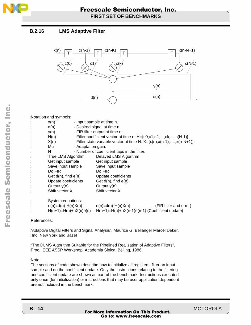
FIRST SET OF BENCHMARKS
Fre
esc
ale
Se
mic
on
du
cto
r, I
Freescale Semiconductor, Inc.n
c..
.
B.2.16 LMS Adaptive Filter
;Notation and symbols:; x(n) - Input sample at time n.; d(n) - Desired signal at time n.; y(n) - FIR filter output at time n.; H(n) - Filter coefficient vector at time n. H=c0,c1,c2,…,ck,…,c(N-1); X(n) - Filter state variable vector at time N. X=x(n),x(n-1),….,x(n-N+1); Mu - Adaptation gain.; N - Number of coefficient taps in the filter. ; True LMS Algorithm Delayed LMS Algorithm; Get input sample Get input sample; Save input sample Save input sample; Do FIR Do FIR; Get d(n), find e(n) Update coefficients; Update coefficients Get d(n), find e(n); Output y(n) Output y(n); Shift vector X Shift vector X
; System equations:; e(n)=d(n)-H(n)X(n) e(n)=d(n)-H(n)X(n) (FIR filter and error); H(n+1)=H(n)+uX(n)e(n) H(n+1)=H(n)+uX(n-1)e(n-1) (Coefficient update)
;References:
;“Adaptive Digital Filters and Signal Analysis”, Maurice G. Bellanger Marcel Deker, ; Inc. New York and Basel
;“The DLMS Algorithm Suitable for the Pipelined Realization of Adaptive Filters”, ;Proc. IEEE ASSP Workshop, Academia Sinica, Beijing, 1986
;Note: ;The sections of code shown describe how to initialize all registers, filter an input ;sample and do the coefficient update. Only the instructions relating to the filtering ;and coefficient update are shown as part of the benchmark. Instructions executed ;only once (for initialization) or instructions that may be user application dependent ;are not included in the benchmark.
T T T T
c(0)
x(n)
c1)
x(n-1)
c(k)
x(n-K)
c(N-1)
x(n-N+1)
y(n)
e(n)d(n)
B - 14 MOTOROLA For More Information On This Product,
Go to: www.freescale.com

FIRST SET OF BENCHMARKS
Fre
esc
ale
Se
mic
on
du
cto
r, I
Freescale Semiconductor, Inc.n
c..
.
; Implementation of the true LMS on the DSP56100 family
;Memory map:
opt ccmove #XM,r0 ;start of Xmove #N-1,m0 ;mod 4 move #-2,n0 ;adjustment for filteringmove m0,m2 ;mod Nmovep x:<<input,y0 ;get input samplemove #H,r3 ;2 2 coefficientsclr a y0,x:(r0)+ ;1 1 save x(n)move x:(r3)+,x1 ;1 1 get c0rep #N-1 ;1 2 do firmac y0,x1,a x:(r0)+,y0 x:(r3)+,x1 ;1 1macr y0,x1,a ;1 1 last tapmovep a,x:<<output ;output fir if desired
;(Get d(n), subtract fir output, multiply by “u”, put the result in x0. ;This section is application dependent.)
move #H,r3 ;1 1 coefficientsmove r3,r2 ;1 1 coefficientsmove x:(r0)+,y0 ;1 1 get x(n)move x:(r3)+,a ;1 1 a=c0do #ntaps,_coefupdate ;2 3 update coef.macr x0,y0,a x:(r0)+,y0 x:(r3)+,x1 ;1 1tfr x1,a a,x:(r2)+ ;1 1 copy c,
_coefupdatemove x:(r0)+n0,y0 ;1 1 update r0move x:(r3)-,y0 ;1 1 update r3
; ________; Totals: 18 3N+17;
X memoryx(n)
x(n-1)..
x(n-N+1)
c0c1c1.
c(N-1)
r0
r3,r2
MOTOROLA B - 15 For More Information On This Product,
Go to: www.freescale.com
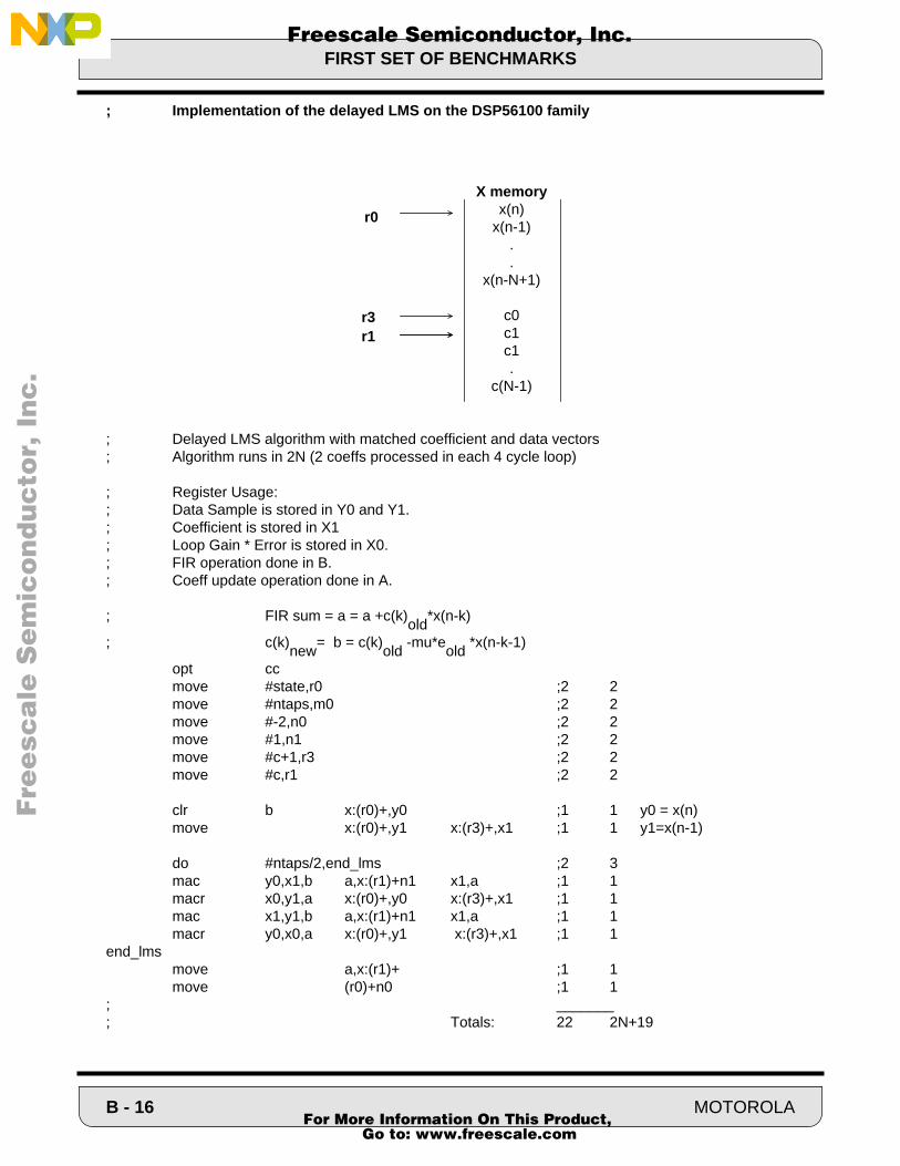
FIRST SET OF BENCHMARKS
Fre
esc
ale
Se
mic
on
du
cto
r, I
Freescale Semiconductor, Inc.n
c..
.
; Implementation of the delayed LMS on the DSP56100 family
; Delayed LMS algorithm with matched coefficient and data vectors; Algorithm runs in 2N (2 coeffs processed in each 4 cycle loop)
; Register Usage:; Data Sample is stored in Y0 and Y1.; Coefficient is stored in X1; Loop Gain * Error is stored in X0.; FIR operation done in B.; Coeff update operation done in A.
; FIR sum = a = a +c(k)old
*x(n-k)
; c(k)new
= b = c(k)old
-mu*eold
*x(n-k-1)
opt ccmove #state,r0 ;2 2move #ntaps,m0 ;2 2move #-2,n0 ;2 2move #1,n1 ;2 2move #c+1,r3 ;2 2move #c,r1 ;2 2
clr b x:(r0)+,y0 ;1 1 y0 = x(n)move x:(r0)+,y1 x:(r3)+,x1 ;1 1 y1=x(n-1)
do #ntaps/2,end_lms ;2 3mac y0,x1,b a,x:(r1)+n1 x1,a ;1 1macr x0,y1,a x:(r0)+,y0 x:(r3)+,x1 ;1 1mac x1,y1,b a,x:(r1)+n1 x1,a ;1 1macr y0,x0,a x:(r0)+,y1 x:(r3)+,x1 ;1 1
end_lmsmove a,x:(r1)+ ;1 1move (r0)+n0 ;1 1
; _______; Totals: 22 2N+19
X memoryx(n)
x(n-1)..
x(n-N+1)
c0c1c1.
c(N-1)
r0
r3r1
B - 16 MOTOROLA For More Information On This Product,
Go to: www.freescale.com
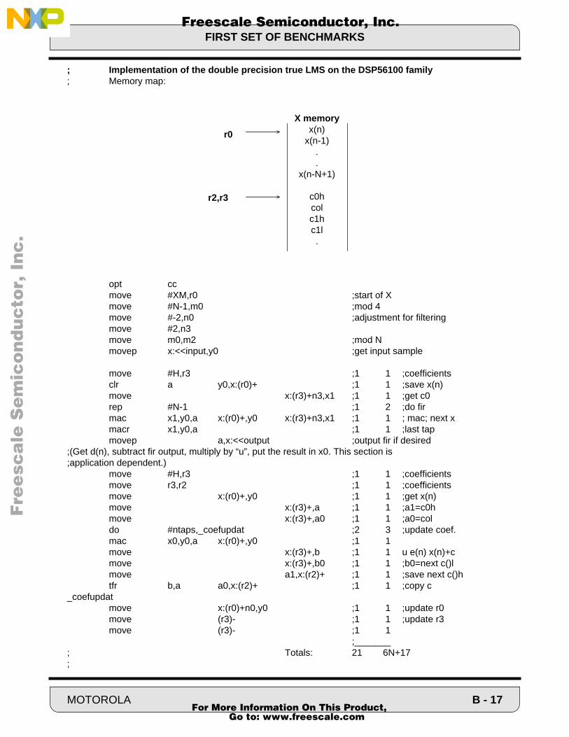
FIRST SET OF BENCHMARKS
Fre
esc
ale
Se
mic
on
du
cto
r, I
Freescale Semiconductor, Inc.n
c..
.
; Implementation of the double precision true LMS on the DSP56100 family; Memory map:
opt ccmove #XM,r0 ;start of Xmove #N-1,m0 ;mod 4move #-2,n0 ;adjustment for filteringmove #2,n3move m0,m2 ;mod Nmovep x:<<input,y0 ;get input sample
move #H,r3 ;1 1 ;coefficientsclr a y0,x:(r0)+ ;1 1 ;save x(n)move x:(r3)+n3,x1 ;1 1 ;get c0 rep #N-1 ;1 2 ;do fir mac x1,y0,a x:(r0)+,y0 x:(r3)+n3,x1 ;1 1 ; mac; next xmacr x1,y0,a ;1 1 ;last tapmovep a,x:<<output ;output fir if desired
;(Get d(n), subtract fir output, multiply by “u”, put the result in x0. This section is ;application dependent.)
move #H,r3 ;1 1 ;coefficientsmove r3,r2 ;1 1 ;coefficientsmove x:(r0)+,y0 ;1 1 ;get x(n)move x:(r3)+,a ;1 1 ;a1=c0hmove x:(r3)+,a0 ;1 1 ;a0=col
do #ntaps,_coefupdat ;2 3 ;update coef. mac x0,y0,a x:(r0)+,y0 ;1 1
move x:(r3)+,b ;1 1 u e(n) x(n)+cmove x:(r3)+,b0 ;1 1 ;b0=next c()lmove a1,x:(r2)+ ;1 1 ;save next c()htfr b,a a0,x:(r2)+ ;1 1 ;copy c
_coefupdatmove x:(r0)+n0,y0 ;1 1 ;update r0move (r3)- ;1 1 ;update r3move (r3)- ;1 1
;_______; Totals: 21 6N+17;
X memoryx(n)
x(n-1)..
x(n-N+1)
c0hcolc1hc1l.
r0
r2,r3
MOTOROLA B - 17 For More Information On This Product,
Go to: www.freescale.com

FIRST SET OF BENCHMARKS
Fre
esc
ale
Se
mic
on
du
cto
r, I
Freescale Semiconductor, Inc.n
c..
.
; Implementation of the double precision delayed LMS on the DSP56100 family
; Delayed LMS algorithm with matched coefficient and data vectors; Algorithm runs in 4N (2 coeffs processed in each 8 cycle loop); Register Usage:; Data Sample is stored in Y0 and Y1.; Coefficient is stored in X1; Loop Gain * Error is stored in X0.; FIR operation done in B.; Coeff update operation done in A.; FIR sum = a = a +c(k)
old*x(n-k)
; c(k)new
= b = c(k)old
-mu*eold
*x(n-k-1)
opt ccmove #state,r0 ;2 2move #ntaps,m0 ;2 2move #-2,n0 ;2 2move #1,n1 ;2 2move #c,r3 ;2 2move #c-2,r1 ;2 2
clr b x:(r0)+,y0 ;1 1 y0 = x(n)move x:(r0)+,y1 x:(r3)+,x1 ;1 1 y1= x(n-1) x1=c0h
do #ntaps/2,end_lms2 ;2 3mac y0,x1,b a,x:(r1)+n1 ;1 1tfr x1,a a0,x:(r1)+n1 ;1 1 a1=ckhmove x:(r3)+,a0 ;1 1 a0=cklmacr x0,y1,a x:(r0)+,y0 x:(r3)+,x1 ;1 1 x1=c(k+1)hmac x1,y1,b a,x:(r1)+n1 ;1 1tfr x1,a a0,x:(r1)+n1 ;1 1move x:(r3)+,a0 ;1 1macr y0,x0,a x:(r0)+,y1 x:(r3)+,x1 ;1 1
end_lms2move a,x:(r1)+ ;1 1move a0,x:(r1)+ ;1 1move (r0)+n0 ;1 1
; _______; Totals: 27 4N+20
X memoryx(n)
x(n-1)..
x(n-N+1)
c0hcolc1hc1l.
r0
r1,r3
B - 18 MOTOROLA For More Information On This Product,
Go to: www.freescale.com

FIRST SET OF BENCHMARKS
Fre
esc
ale
Se
mic
on
du
cto
r, I
Freescale Semiconductor, Inc.n
c..
.
;-------------------------------------------------------------------------------------------------------------------------------------------; The complete code for a true LMS that executes in two instruction cycles per tap is shown below.; A brief description of how the algorithm is derived precedes the LMS code. Note that the coefficients ; stored to memory are saturated (should overflow occur), whereas the coefficients used in the FIR; filter are not; saturated. Therefore, the coefficients stored to memory, and the coefficients used in the FIR filter; calculation,; are not guaranteed to be the same. This should not be a problem in designs where the echo gain; is guaranteed; to be less than one.;-------------------------------------------------------------------------------------------------------------------------------------------
opt cc,cexpage 132,66section FAST_LMS
n_tap equ 16org x:$0100
ref_buf dsm n_tap ;Ref_buf is a modulo n_tap buffer, containing;a reference signal.
coeff ds n_tap ;Note: Coefficients are stored in reverse order
ref_ptr dc ref_buf ;data pointer for reference bufferscaled_error dc 0 ;scaled error sample from last call of echo_inputnorm_factor dc 0.1 ;scale factor for error signal
org p:0jmp Test_ECorg p:$0100
;-------------------------------------------------------------------------------------------------------------------------------------------;; The following pseudo code is for the “standard” LMS echo canceller algorithm.; y(n) = estimate of echo at time sample n.; x(n) = reference input signal at time n.; input (n) = input signal (containing echo signal) at time n.; c(n,k) = k’th coefficient at time n.;; /* initialize N coefficients at time 0 to 0 */;; for (k = 0 to n-1) ; c(0,k) = 0;; ;; /* LMS follows, do forever */;; n = 0;; do forever ; y(n) = 0;;; for (k=0 to N-1) ; y(n) = y(n) + c(n,k)*x(n-k); /* FIR filter */; ;; error(n) = input(n) - y(n);;; for (k = 0 to N-1) ; c(n+1,k) = c(n,k) + delta*error(n)*x(n-k) ; /* Coefficient Update */;; ;; n = n+1;; ;--------------------------------------------------------------------------------------------------------------------------------------------
MOTOROLA B - 19 For More Information On This Product,
Go to: www.freescale.com

FIRST SET OF BENCHMARKS
Fre
esc
ale
Se
mic
on
du
cto
r, I
Freescale Semiconductor, Inc.n
c..
.
;-------------------------------------------------------------------------------------------------------------------------------------------; The following is equivalent to the above (i.e., given the same input signals, the error signal and ; coefficients will follow the exact same trajectories. Note the calculations are run from the back of; the filter to the front. This saves two registers. Also note that the calculation order of the coefficient; and the FIR filter has been reversed.;; /* initialize N coefficients at time -1 to 0 */;; for (k = 0 to N-1) ; c(-1,k) = 0;; ;; error (-1) = 0 ;The initial error must be set to zero.;; /* LMS follows, do forever */;; n = 0;; do forever ;; y(n) = 0;;; for (k = N-1 to 0) ; c(n,k) = c(n-1,k) + delta*error(n-1)*x(n-1-k); /* Coefficient */; ;; for (k= N-1to 0) ; y(n) = y(n) + c(n,k)*x(n-k); /* FIR filter */; ;; error(n) = input(n) - y(n);;; n = n+1;;; ;-------------------------------------------------------------------------------------------------------------------------------------------; Note that the two “for” loops in the do forever loop can now be combined.;-------------------------------------------------------------------------------------------------------------------------------------------;; /* initialize N coefficients at time -1 to 0 */;; for (k = 0 to N-1) ; c(-1,k) = 0;; ;; error(-1) = 0;;; /* LMS follows, do forever */;; n = 0;; do forever ;; y(n) = 0;;; for (k = N-1 to 0) ; c(n,k) = c(n-1,k) + delta*error(n-1)*x(n-1-k); /* Coefficient */; y(n) = y(n) + c(n,k)*x(n-k); /* FIR filter */; ;; error(n) = input(n) - y(n);;; n = n+1;;; ;-------------------------------------------------------------------------------------------------------------------------------------------
B - 20 MOTOROLA For More Information On This Product,
Go to: www.freescale.com

FIRST SET OF BENCHMARKS
Fre
esc
ale
Se
mic
on
du
cto
r, I
Freescale Semiconductor, Inc.n
c..
.
;-------------------------------------------------------------------------------------------------------------------------------------------;; Echo Canceller Routine (Fast LMS);; Upon Entry; x1 should contain newest reference sample; y1 should contain newest input sample;; Upon Exit; b will contain echo cancelled output;; Note that the coefficients are stored in reverse time order.;-------------------------------------------------------------------------------------------------------------------------------------------
FAST_LMS:
move #+1,n1
move #n_tap-1,m0move #-1,m1move m1,m3
move x:ref_ptr,r0 ;r0 is the get reference signal pointer
move #coeff,r3 ;r3 is the get coefficient pointermove r3,r1 ;r1 is the put coefficient pointer
move x:(r0),y0 ;y0 contains the oldest reference samplemove x1,x:(r0)+ ;store newest reference sample in reference register
clr b x:(r3)+,a ;fetch first coefficient, and clear b for FIRmove x:scaled_error,x0 ;x0 is the scaled error sample
do #n_tap,end_fir_update
macr x0,y0,a x:(r0)+,y0 x:(r3)+,x1mac a1,y0,b a,x:(r1)+n1 x1,a
end_fir_update
neg bmove r0,x:ref_ptr ;store get reference pointeradd y1,b ;b = EC output = input - echo_estimate
move x:norm_factor,x0move b,y0mpyr y0,x0,amove a,x:scaled_error
move b,x:output_port
rts
MOTOROLA B - 21 For More Information On This Product,
Go to: www.freescale.com

FIRST SET OF BENCHMARKS
Fre
esc
ale
Se
mic
on
du
cto
r, I
Freescale Semiconductor, Inc.n
c..
.
;-------------------------------------------------------------------------------------------------------------------------------------------;; Test shell follows; Remote signal is an impulse train, period greater than echo span; Input is the resulting echo signal;;-------------------------------------------------------------------------------------------------------------------------------------------
org x:$1000
output_port ds 1 ;write output to D/A
org x:$0400
Remote_signal dc 0.8dc 0.0dc 0.0dc 0.0dc 0.0dc 0.0dc 0.0dc 0.0dc 0.0dc 0.0dc 0.0dc 0.0dc 0.0dc 0.0dc 0.0dc 0.0dc 0.0dc 0.0dc 0.0dc 0.0
org c:$0420
echo_input dc 0.0dc 0.0dc 0.2dc 0.4dc 0.7dc 0.4dc 0.2dc 0.1dc 0.0dc -0.1dc -0.2dc -0.1dc 0.0dc 0.1dc 0.0dc 0.0dc 0.0dc 0.0dc 0.0dc 0.0
remote_get dc remote_signalinput_get dc echo_input
B - 22 MOTOROLA For More Information On This Product,
Go to: www.freescale.com
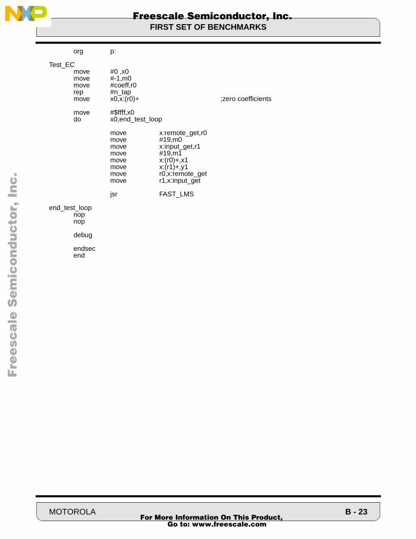
FIRST SET OF BENCHMARKS
Fre
esc
ale
Se
mic
on
du
cto
r, I
Freescale Semiconductor, Inc.n
c..
.
org p:
Test_ECmove #0 ,x0move #-1,m0move #coeff,r0rep #n_tapmove x0,x:(r0)+ ;zero coefficients
move #$ffff,x0do x0,end_test_loop
move x:remote_get,r0move #19,m0move x:input_get,r1move #19,m1move x:(r0)+,x1move x:(r1)+,y1move r0,x:remote_getmove r1,x:input_get
jsr FAST_LMS
end_test_loopnopnop
debug
endsecend
MOTOROLA B - 23 For More Information On This Product,
Go to: www.freescale.com

FIRST SET OF BENCHMARKS
Fre
esc
ale
Se
mic
on
du
cto
r, I
Freescale Semiconductor, Inc.n
c..
.
B.2.17 FIR Lattice Filter
;Lattice filter benchmarks. N refers to the number of “k” coefficients in the lattice filter. ;Some filters may have other coefficients other than the “k” coefficients but their; number may be determined from k.
; move #state,r0 ;point to state variable storagemove #N,m0 ;N=number of k coefficientsmove #k,r1 ;point to k coefficientsmove #N-1,m1 ;mod for k’smove #0,n0opt cc
movep x:<<input,b ;get input
move b,x:(r0)+ ;1 1 save 1st statemove x:(r1)+,x0 ;1 1 get k do #N,end_elat ;2 3move x:(r0)+n0,a b,y0 ;1 1 get s;copy t macr x0,y0,a x:(r0)+n0,x1 ;1 1 t*k+s, copy s
macr x1,x0,b x:(r1)+,x0 ;1 1 ;s*k+t, nxt kmove a,x:(r0)+ ;1 1 ;sv st
end_elatmove x:(r0)-,y1 ;1 1move x:(r1)-,x0 ;1 1movep b,x:<<output ;output
; _______; 10 4N+7;
K1
x(n)
S1
T
K2
S2
T
K3
S3
TSx
K
S
TS’
t’t
SINGLE SECTION X memoryS1S2S3Sx
K1K2K3
r0
r1
FIR LATTICE FILTER
The equations are:
t’ = s*t + t ; t’→ ts’ = t*k + s’
B - 24 MOTOROLA For More Information On This Product,
Go to: www.freescale.com

FIRST SET OF BENCHMARKS
Fre
esc
ale
Se
mic
on
du
cto
r, I
Freescale Semiconductor, Inc.n
c..
.
B.2.18 All Pole IIR Lattice Filter
opt ccmove #k+N-1,r0 ;point to kmove #N-1,m0 ;number of k’s-1move #-1,n1move n1,n3movep x:<<input,a ;get input samplemove #state,r3 ;2 2 pt to x() move x:(r0)-,y1 ;1 1 y1=k3move x:(r3)+,x1 ;1 1 x1=s3macr -x1,y1,a x:(r0)+n0,y1 ;1 1 a=in-k3s3;y1=k2move x:(r3)-,x1 ;1 1 x1=s2do #n-1,endlat ;2 3macr -x1,y1,a b,x:(r3)+ ;1 1 a=a-s2k2=t2;update s3move x:(r3)+,b a,x1 ;1 1 b=s2macr x1,y1,b x:(r0)+n0,y1 x:(r3)+n3,x1 ;1 1 b=s2+t2k2;get s1,k1
endlatmove b,x:(r3)+ ;1 1 sv 2nd last smove x:(r0)+,y1 ;1 1 update r0 move a,x:(r3)+ ;1 1 save last smovep a,x:<<output ; output
; ________; Total: 14 3N+12;
-K3
x(n)
-K2
S2
T T
t’t
SINGLE SECTION X memoryS3S2S1
K1K2K3
r3
r0
ALL POLE IIR LATTICE FILTER
The equations are:
t’ = t-s*k ; t’→ ts’ = t*k + s’
K2
-K1
S1
T
K1
-K
s
K
s’T
MOTOROLA B - 25 For More Information On This Product,
Go to: www.freescale.com

FIRST SET OF BENCHMARKS
F
ree
sca
le S
em
ico
nd
uc
tor,
I
Freescale Semiconductor, Inc.n
c..
.
B.2.19 General Lattice Filter
opt ccmove #k,r0 ;point to coefficientsmove #2*N,m0 ;mod 2*(# of k’s)+1move #-1,n3movep x:<<input,a ;get input samplemove #state,r3 ;2 2 ;pto filter statesmove x:(r0)+,y1 ;1 1 ;get first kmove x:(r3)-,x1 ;1 1 ;first s
do #N,el ;2 3 ;do filter macr -y1,x1,a b,x:(r3)+ ;1 1 ;t-k*s, save s
move x:(r3)+,b a,x1 ;1 1 ;get s again macr x1,y1,b x:(r0)+,y1 x:(r3)+n3,x1 ;1 1 ;t’*k+s,get k& sel move b,x:(r3)+ ;1 1 ;s 2nd to1st st clr a a,x:(r3)+ ;1 1 ;s first state
move x:(r3)+,x1 ;1 1 ;get last state rep #N ;1 2 ;do fir taps mac y1,x1,a x:(r0)+,y1 x:(r3)+,x1 ;1 1
macr y1,x1,a x:(r3)+,x1 ;1 1 finish, adj pointer movep a,x:<<output ;_______output sample
; Totals: 15 4N+13;
-K3
x(n)
-K2
S2
T T
t’t
SINGLE SECTION
X memory
K3K2K1W3W2W1W0
S3S2S1
r0
r3
GENERAL LATTICE FILTER
The equations are:
t’ = t-s*k ; t’→ ts’ = t*k + s’
output = Σ s’*w
K2
-K1
S1
T
K1
-K
s
K
s’T
S3
w3 w2 w1
w
B - 26 MOTOROLA For More Information On This Product,
Go to: www.freescale.com

FIRST SET OF BENCHMARKS
F
ree
sca
le S
em
ico
nd
uc
tor,
I
Freescale Semiconductor, Inc.n
c..
.
B.2.20 Normalized Lattice Filter
opt ccmove #c,r0 ;point to coefficientsmove #3*N,m0 ;mod on coefficientsmove #0,n3movep x:<<input,a ;get input samplemove #state,r3 ;2 2 pt to state move x:(r0)+,y1 a,x1 ;1 1 get first Q do #n,endnlat ;2 3mpy x1,y1,a x:(r0)+,y0 x:(r3)+n3,x0 ;1 1 ;q*t; get k & smacr -x0,y0,a b,x:(r3)+ ;1 1 ;q*t-k*s,save smpy y0,x1,b a,x1 ;1 1 ;k*t, set t’ macr y1,x0,b x:(r0)+,y1 ;1 1 ;k*t+q*s, get q
endnlatmove b,x:(r3)+ ;1 1 ;sv scnd lst st move a,x:(r3)+ ;1 1 ;save stateclr a x:(r3)+,x1 ;1 1 ;clr accrep #n ;1 2 ;do fir taps
mac x1,y1,a x:(r0)+,y1 x:(r3)+,x1 ;1 1 macr x1,y1,a x:(r3)+,x1 ;1 1 rnd, adj pointer
movep a,x:<<output ;______ output sample; Totals: 15 5N+12;
x(n)
t’t
SINGLE SECTION
X memory
q2k2q1k1q0k0w3w2w1w0SxS2S1S0
r0
r3
The equations are:
t’ = t*q - s*k ; t’→ tu’ = t*k + s’*q
output = Σ u’*w
-K
s
K
u’T
w
q
q
u
-K2
s2
K2
T
w3
q2
q2
-K1
s1
K1
T
w2
q1
q1
-K0
s0
K0
T
w1
q0
q0
w0
MOTOROLA B - 27 For More Information On This Product,
Go to: www.freescale.com
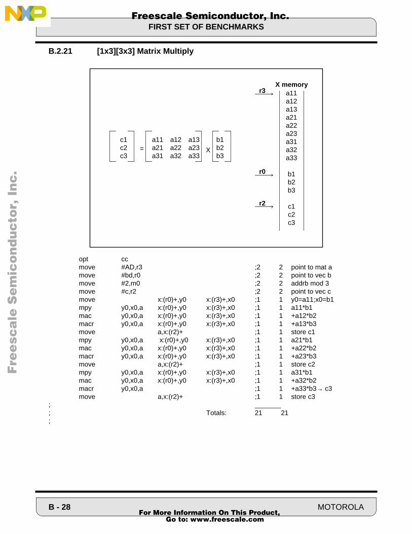
FIRST SET OF BENCHMARKS
F
ree
sca
le S
em
ico
nd
uc
tor,
I
Freescale Semiconductor, Inc.n
c..
.
B.2.21 [1x3][3x3] Matrix Multiply
opt ccmove #AD,r3 ;2 2 point to mat amove #bd,r0 ;2 2 point to vec bmove #2,m0 ;2 2 addrb mod 3move #c,r2 ;2 2 point to vec cmove x:(r0)+,y0 x:(r3)+,x0 ;1 1 y0=a11;x0=b1mpy y0,x0,a x:(r0)+,y0 x:(r3)+,x0 ;1 1 a11*b1mac y0,x0,a x:(r0)+,y0 x:(r3)+,x0 ;1 1 +a12*b2macr y0,x0,a x:(r0)+,y0 x:(r3)+,x0 ;1 1 +a13*b3move a,x:(r2)+ ;1 1 store c1mpy y0,x0,a x:(r0)+,y0 x:(r3)+,x0 ;1 1 a21*b1mac y0,x0,a x:(r0)+,y0 x:(r3)+,x0 ;1 1 +a22*b2macr y0,x0,a x:(r0)+,y0 x:(r3)+,x0 ;1 1 +a23*b3move a,x:(r2)+ ;1 1 store c2mpy y0,x0,a x:(r0)+,y0 x:(r3)+,x0 ;1 1 a31*b1mac y0,x0,a x:(r0)+,y0 x:(r3)+,x0 ;1 1 +a32*b2macr y0,x0,a ;1 1 +a33*b3→ c3move a,x:(r2)+ ;1 1 store c3
; _______; Totals: 21 21;
c1c2c3
a11 a12 a13a21 a22 a23a31 a32 a33
a11a12a13a21a22a23a31a32a33
b1b2b3
c1c2c3
b1b2b3
X=
X memoryr3
r0
r2
B - 28 MOTOROLA For More Information On This Product,
Go to: www.freescale.com

FIRST SET OF BENCHMARKS
F
ree
sca
le S
em
ico
nd
uc
tor,
I
Freescale Semiconductor, Inc.n
c..
.
B.2.22 [NxN][NxN] Matrix Multiply
;The matrix multiplications are for square NxN matrices.
;All the elements;are stored in “row major” format. i.e. for the array A:
opt ccmove #AD,r0 ;2 2 point to A move #bd,r3 ;2 2 ;point to Bmove #c,r2 ;2 2 ;output mat Cmove #N,b ;2 2 ;array sizemove b,n3 ;1 1
do #N,erows ;2 3 do rows do #N,ecols ;2 3 do columnsmove x1,r0 ;1 1 copy row Amove r1,r3 ;1 1 copy col Bclr a x:(r0)+,y0 ;1 1move x:(r3)+n3,x0 ;1 1 clr sum & piperep #N-1 ;1 2 sum mac y0,x0,a x:(r0)+,y0 x:(r3)+n3,x0 ;1 1macr y0,x0,a x:(r3)+,y1 ;1 1 finish, next col
move a,x:(r2)+ ;1 1 ;save output ecols
add x1,b ;1 1 next row A move b,x1 ;1 1move #bd,r1 ;2 2 first element B
erows; _______; Total: Words: Cycles:; 25 ((8+(N-1))N+7)N+12)
; N3+7N
2+6N+8
;
a11.
a1k.
ak1.
aN1.
b11..
c11
X
=
X memoryr3
r0
r2
c11 .. c1k .. c1N.ck1 .. ckk .. ckN.cN1 .. cNk .. cNN
b11 .. b1k .. b1N.bk1 .. bkk .. bkN.bN1 .. bNk .. bNN
a11 .. a1k .. a1N.ak1 .. akk .. akN.aN1 .. aNk .. aNN
MOTOROLA B - 29 For More Information On This Product,
Go to: www.freescale.com

FIRST SET OF BENCHMARKS
F
ree
sca
le S
em
ico
nd
uc
tor,
I
Freescale Semiconductor, Inc.n
c..
.
B.2.23 N Point 3x3 2-D FIR Convolution
;The two dimensional FIR uses a 3x3 coefficient mask:
;;The image is an array of 512x512 pixels. To provide boundary conditions for the FIR filtering, the;image is surrounded by a set of zeros such that the image is actually stored as a 514x514 array. i.e.;
;;The image (with boundary) is stored in row major storage. The first element of the ;array image is image(1,1) followed by image(1,2). The last element of the first row is image(1,514);followed by the beginning of the next column image(2,1). These are stored sequentially in the array; “im” in d memory.;;Image(1,1) maps to index 0, image(1,514) maps to index 513,;Image(2,1) maps to index 514 (row major storage).;;Although many other implementations are possible, this is a realistic type of image environment;where the actual size of the image may not be an exact power of 2. ;Other possibilities include storing a 512x512image but computing only a 511x511;result, computing a 512x512 result without boundary conditions but throwing away the pixels on;the border, etc.
; r0 → image(n,m) image(n,m+1) image(n,m+2); r1 → image(n+514,m) image(n+514,m+1 image(n+514,m+2); r2 → image(n+2*514,m) image(n+2*514,m+2) image(n+2*514,m+3); r3 → FIR coefficients; b → output image
c11 c12 c13c21 c22 c23c31 c32 c33
0 0 0
0 0
0 image 0area
0 0 0
514 512
514
B - 30 MOTOROLA For More Information On This Product,
Go to: www.freescale.com

FIRST SET OF BENCHMARKS
F
ree
sca
le S
em
ico
nd
uc
tor,
I
Freescale Semiconductor, Inc.n
c..
.
opt ccmove #mask,r3 ;2 2 pt to coef.move #-8,n3 ;2 2move #image,r0 ;2 2 top boundarymove #image+514,r1 ;2 2 left of first pixelmove #image+2*514,r2 ;2 2 left of 2nd row
move #512,y1 ;2 2move #-1,n1 ;2 2 adjust.move n1,n2 ;1 1
move #output,b ;2 2 output imagemove x:(r0)+,y0 ;1 1 y0=im(1,1) move x:(r3)+,x0 ;1 1 x0=c11
do y1,rows ;2 3do y1,cols ;2 3mpy y0,x0,a x:(r0)+,y0 x:(r3)+,x0 ;1 1 im(1,1)*c11mac y0,x0,a x:(r0)+n0,y0 x:(r3)+,x0 ;1 1 +im(1,2)*c12 mac y0,x0,a x:(r1)+,y0 x:(r3)+,x0 ;1 1 +im(1,3)*c13mac y0,x0,a x:(r1)+,y0 x:(r3)+,x0 ;1 1 +im(2,1)*c21mac y0,x0,a x:(r1)+n1,y0 x:(r3)+,x0 ;1 1 +im(2,2)*c22mac y0,x0,a x:(r2)+,y0 x:(r3)+,x0 ;1 1 +im(2,3)*c23mac y0,x0,a x:(r2)+,y0 x:(r3)+,x0 ;1 1 +im(3,1)*c31mac y0,x0,a x:(r2)+n2,y0 x:(r3)+n3,x0 ;1 1 +im(3,2)*c32macr y0,x0,a x:(r0)+,y0 x:(r3)+,x0 ;1 1 +im(3,3)*c33move a,x:(b1) ;1 2inc24 b ;1 1
cols; adjust pointers for frame boundary
move #2,n1 ;2 2move n1,n2 ;1 1inc b x:(r0)+,x1 ;1 1 adj r0 inc b x:(r1)+n1,x1 ;1 1 adj r1 move (r2)+n2 ;1 1 adj r2move x:(r0)+,x1 ;1 1 preloadmove #-1,n1 ;2 2 ;adjust. move n1,n2 ;1 1
rows ;________
; Totals: 44 12N2+13N+22
; Kernel: 12;
MOTOROLA B - 31 For More Information On This Product,
Go to: www.freescale.com

FIRST SET OF BENCHMARKS
F
ree
sca
le S
em
ico
nd
uc
tor,
I
Freescale Semiconductor, Inc.n
c..
.
B.2.24 Signed 16 Bit Result Divide
;This is a routine for a 4 quadrant divide (i.e., a signed divisor and a signed dividend)
;which generated a 16-bit signed quotient and a 32-bit signed remainder. The
;quotient is stored in the lower 16 bits of accumulator a, a0, and the remainder in
;the upper 16 bits a1. The true (restored) remainder is stored in b1. The original
;dividend must occupy the low order 32 bits of the destination accumulator, a, and
;must be a POSITIVE number. The divisor must be larger than the dividend so that a
;fractional quotient is generated.
opt ccabs a a,b ;1 1 make dividend positivemove b,x:$0 ;2 2 save rem. sign in x:$0eor x0,b ;1 1 quo. sign in N bit of CCRandi #$fe,ccr ;1 1 clear carry bit C (quotient sign bit)rep #$10 ;1 2 form a 16-bit quotientdiv x0,a ;1 1 form quot. in a0, remainder in a1tfr a,b ;1 1 save remainder and quot. in b1,b0jpl savequo ;1 2 go to savequo if quot. is positiveneg b ;1 1 complement quotient if N bit is set
savequo tfr x0,b ;1 1 get signed divisormove b0,x1 ;1 1 save quo. in x1abs b ;1 1 get abs value of signed divisoradd a,b ;1 1 restore remainder in b1bftstl #$8000,x:$0 ;2 2 test if remainder is positivebeq <done1 ;1 2 branch if positivemove #$0,b0 ;1 1 prevent unwanted carryneg b ;1 1 complement remainder
done1 ;end of routine.; ;________; total 19 37;
B - 32 MOTOROLA For More Information On This Product,
Go to: www.freescale.com
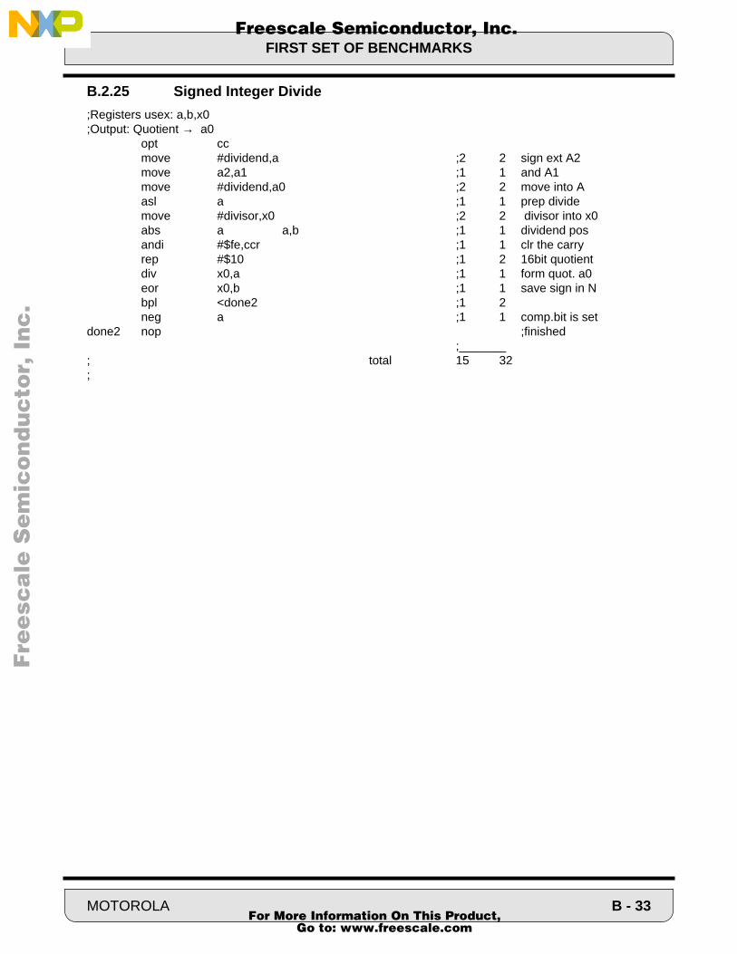
FIRST SET OF BENCHMARKS
F
ree
sca
le S
em
ico
nd
uc
tor,
I
Freescale Semiconductor, Inc.n
c..
.
B.2.25 Signed Integer Divide
;Registers usex: a,b,x0;Output: Quotient → a0
opt ccmove #dividend,a ;2 2 sign ext A2 move a2,a1 ;1 1 and A1move #dividend,a0 ;2 2 move into Aasl a ;1 1 prep dividemove #divisor,x0 ;2 2 divisor into x0abs a a,b ;1 1 dividend posandi #$fe,ccr ;1 1 clr the carryrep #$10 ;1 2 16bit quotientdiv x0,a ;1 1 form quot. a0eor x0,b ;1 1 save sign in Nbpl <done2 ;1 2neg a ;1 1 comp.bit is set
done2 nop ;finished;_______
; total 15 32;
MOTOROLA B - 33 For More Information On This Product,
Go to: www.freescale.com
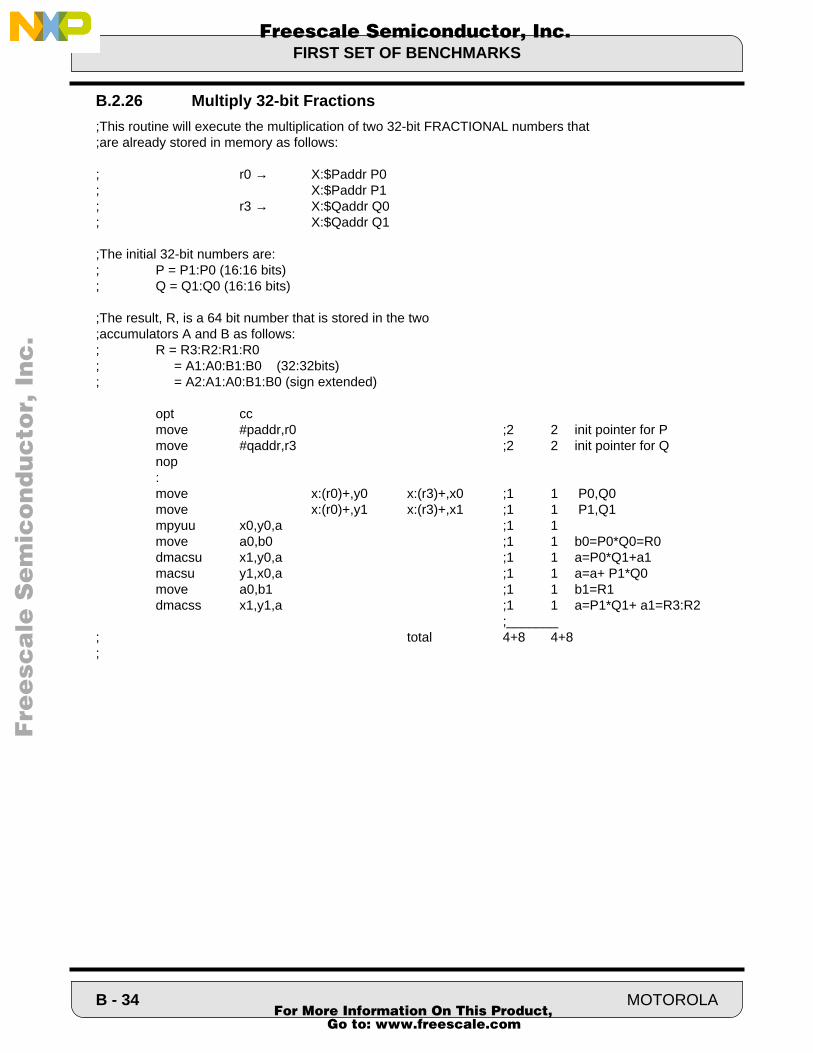
FIRST SET OF BENCHMARKS
F
ree
sca
le S
em
ico
nd
uc
tor,
I
Freescale Semiconductor, Inc.n
c..
.
B.2.26 Multiply 32-bit Fractions
;This routine will execute the multiplication of two 32-bit FRACTIONAL numbers that ;are already stored in memory as follows:
; r0 → X:$Paddr P0; X:$Paddr P1; r3 → X:$Qaddr Q0; X:$Qaddr Q1
;The initial 32-bit numbers are:; P = P1:P0 (16:16 bits); Q = Q1:Q0 (16:16 bits)
;The result, R, is a 64 bit number that is stored in the two;accumulators A and B as follows:; R = R3:R2:R1:R0; = A1:A0:B1:B0 (32:32bits); = A2:A1:A0:B1:B0 (sign extended)
opt ccmove #paddr,r0 ;2 2 init pointer for Pmove #qaddr,r3 ;2 2 init pointer for Qnop:move x:(r0)+,y0 x:(r3)+,x0 ;1 1 P0,Q0move x:(r0)+,y1 x:(r3)+,x1 ;1 1 P1,Q1mpyuu x0,y0,a ;1 1move a0,b0 ;1 1 b0=P0*Q0=R0dmacsu x1,y0,a ;1 1 a=P0*Q1+a1macsu y1,x0,a ;1 1 a=a+ P1*Q0move a0,b1 ;1 1 b1=R1dmacss x1,y1,a ;1 1 a=P1*Q1+ a1=R3:R2
;_______; total 4+8 4+8;
B - 34 MOTOROLA For More Information On This Product,
Go to: www.freescale.com

SECOND SET OF BENCHMARKS
F
ree
sca
le S
em
ico
nd
uc
tor,
I
Freescale Semiconductor, Inc.n
c..
.
B.3 SECOND SET OF BENCHMARKS
B.3.1 Sine Wave Generation Using Double Integration Technique
opt ccclr b ;1 1move #$4000,a ;2 2move #0,n1 ;2 2
move #$4532,x1 ;2 2move #$1,r1 ;2 2move x0,y0 ;1 1
do y1,loop1 ;2 3mac x0,b1,a b,x:(r1)+n1 ;1 1mac -y0,a1,b ;1 1
loop1move b,x:(r1) ;1 1
; _______; 15 2N+14;
T T
x0
sin(w0t)
a
a= Stored initial value which is the desired tone amplitude
x0 = 2*sin(πFs/F0)F0 = Oscillation FrequencyFs = Sampling Frequency
MOTOROLA B - 35 For More Information On This Product,
Go to: www.freescale.com

SECOND SET OF BENCHMARKS
F
ree
sca
le S
em
ico
nd
uc
tor,
I
Freescale Semiconductor, Inc.n
c..
.
B.3.2 Sine Wave Generation Using Second Order Oscillator
opt ccclr a ;1 1move #$4000,x1 ;2 2
move #$6d4b,x0 ;2 2move #$1,r1 ;2 2move #0,n1 ;2 2
do y1,loop2 ;2 3mac -x1,x0,a x1,x:(r1)+n1 ;1 1neg a ;1 1mac x1,x0,a ;1 1tfr x1,a a,x1 ;1 1
loop2move x1,x:(r1) ;1 1
;______; 16 4N+13;
T T
x0
sin(w0t)
a
a= Stored initial value which is the desired tone amplitude
x0 = 2*cos(2πFs/F0)F0 = Oscillation FrequencyFs = Sampling Frequency
-
B - 36 MOTOROLA For More Information On This Product,
Go to: www.freescale.com

SECOND SET OF BENCHMARKS
F
ree
sca
le S
em
ico
nd
uc
tor,
I
Freescale Semiconductor, Inc.n
c..
.
B.3.3 IIR Filter Using Cascaded Transpose BIQUAD Cell
opt ccmove #w1,r0move #w2,r1move #N-1,m0move m0,m1move #0,n0move #0,n1move #c,r3ori #08,mrmove x:(r0)+n0,b x:(r3)+,x0 ;1 1 b=w1;x0=b0/2asr b ;1 1 b=w1/2
movep x:<<input,y0 ;1 2 y0=x
do #N,end_lp ;2 3macr y0,x0,b x:(r1)+n1,a x:(r3)+,x0 ;1 1 b=y/2;get w2,b1/2asr a b,y1 ;1 1 a=w2/2;y1=ymac x0,y0,a x:(r3)+,x0 ;1 1 a=x*b1/2+w2/2,get a1/2macr x0,y1,a x:(r3)+,x0 ;1 1 a=w1/2;get b2/2mpy x0,y0,a a,x:(r0)+ ;1 1 a=x*b2/2;save w1 move x:(r3)+,x0 b,y0 ;1 1 y0=y;get a2/2macr y1,x0,a x:(r0)+n0,b x:(r3)+,x0 ;1 1 a=w2/2
;get next w1, next b0/2asr b a,x:(r1)+ ;1 1 b=w1/2; save w2
end_lpmovep y0,x:<<output ;1 2 output y
; ______; 14 8N+9
T
x(n) y(n)
T
w1(n)
w2(n)- a2
- a1
b2
b1
b0
1 + a1 z-1 + a2 z-2
b0 + b1 z-1 + b2 z-2
H(z) =
NEQUATION:y(n) = b0*x(n) + w1(n-1)w1(n) = b1*x(n) - a1*y(n) + w2(n-1)w2(n) = b2*x(n) - a2*y(n)
IMPLEMENTATION:y(n)/2 = b0/2*x(n) + w1(n-1)/2w1(n)/2 = b1/2*x(n) - a1/2*y(n) + w2(n-1)/2w2(n)/2 = b2/2*x(n) - a2/2*y(n)
w11(n-1)w12(n-1)
.
.w21(n-1)w22(n-1)
.
.b1(0)/2b1(1)/2
- a1(1)/2b1(2)/2
- a1(2)/2..
X memory
r3
r0
r1
MOTOROLA B - 37 For More Information On This Product,
Go to: www.freescale.com

SECOND SET OF BENCHMARKS
F
ree
sca
le S
em
ico
nd
uc
tor,
I
Freescale Semiconductor, Inc.n
c..
.
IIR Filter Using The Nth Order Direct Form II Canonic
;The equation of the filter becomes:
; wn = a0*xn - a1*wn-1 - a2*wn-2........... - aN*wn-N; yn = b0*wn +b1*wn-1 + b2*wn-2...........+ bN*wn-N
opt ccmove #c,r3move #(N*2+1), m3move #w,r0move #N,m0move #0,n0
movep x:<<input,y0 ;1 2 y0=xnclr a x:(r3)+,x1 ;1 1 x1=a1rep #N ;1 2mac y0,x1,a x:(r0)+,y0 x:(r3)+,x1 ;1 1macr y0,x1,a x:(r3)+,x1 ;1 1 a=wn, x1=b0clr a a,x:(r0)+n0 ;1 1move x:(r0)+,y0 ;1 1 y0=wnrep #N ;1 2mac y0,x1,a x:(r0)+,y0 x:(r3)+,x1 ;1 1macr y0,x1,a ;1 1 a=yn
movep a,x:<<output ;1 2 output y; ; ; 11 2N+13 filter loop;
T
x(n) y(n)
T
w(n-1)
w(n-2)
w(n-1)w(n-2)w(n-3)
.
.
.w(n-N)
a0- a1
.
.b0b1..
X memory
r3
r0
T
w(n-N)
- a2
- a1
a0
- aN
w(n)
b2
b1
b0
bN H z( )
bizi–
i 0=
N
∑
aizi–
i 0=
N
∑--------------------=
B - 38 MOTOROLA For More Information On This Product,
Go to: www.freescale.com
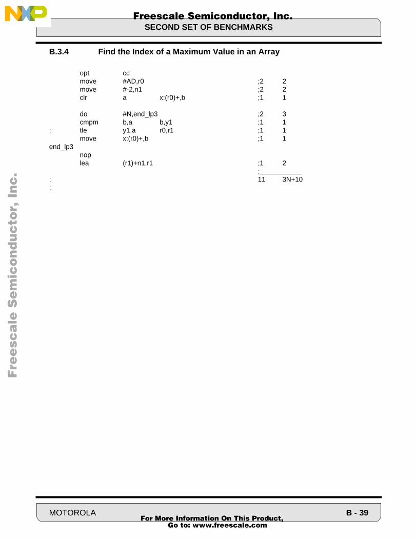
SECOND SET OF BENCHMARKS
F
ree
sca
le S
em
ico
nd
uc
tor,
I
Freescale Semiconductor, Inc.n
c..
.
B.3.4 Find the Index of a Maximum Value in an Array
opt ccmove #AD,r0 ;2 2move #-2,n1 ;2 2clr a x:(r0)+,b ;1 1
do #N,end_lp3 ;2 3cmpm b,a b,y1 ;1 1
; tle y1,a r0,r1 ;1 1move x:(r0)+,b ;1 1
end_lp3noplea (r1)+n1,r1 ;1 2
; ; 11 3N+10;
MOTOROLA B - 39 For More Information On This Product,
Go to: www.freescale.com
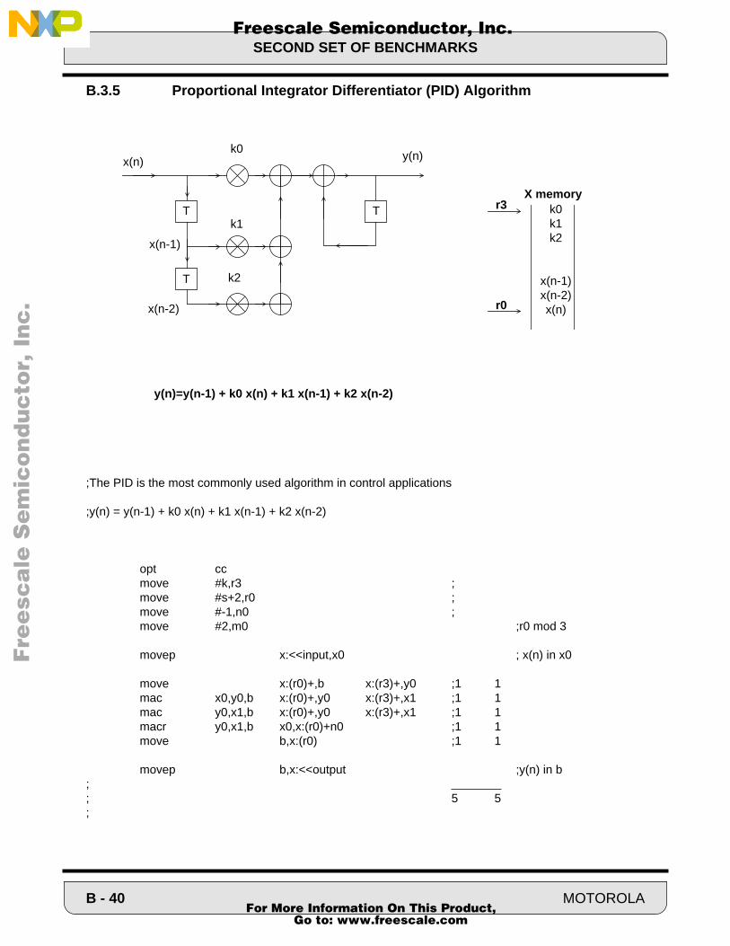
SECOND SET OF BENCHMARKS
F
ree
sca
le S
em
ico
nd
uc
tor,
I
Freescale Semiconductor, Inc.n
c..
.
B.3.5 Proportional Integrator Differentiator (PID) Algorithm
;The PID is the most commonly used algorithm in control applications
;y(n) = y(n-1) + k0 x(n) + k1 x(n-1) + k2 x(n-2)
opt ccmove #k,r3 ;move #s+2,r0 ;move #-1,n0 ;move #2,m0 ;r0 mod 3
movep x:<<input,x0 ; x(n) in x0
move x:(r0)+,b x:(r3)+,y0 ;1 1mac x0,y0,b x:(r0)+,y0 x:(r3)+,x1 ;1 1mac y0,x1,b x:(r0)+,y0 x:(r3)+,x1 ;1 1macr y0,x1,b x0,x:(r0)+n0 ;1 1move b,x:(r0) ;1 1
movep b,x:<<output ;y(n) in b; ; 5 5;
T T
x(n) y(n)
T
x(n-1)
x(n-2)
k2
k1
k0
y(n)=y(n-1) + k0 x(n) + k1 x(n-1) + k2 x(n-2)
k0k1k2
x(n-1)x(n-2)x(n)
X memoryr3
r0
B - 40 MOTOROLA For More Information On This Product,
Go to: www.freescale.com
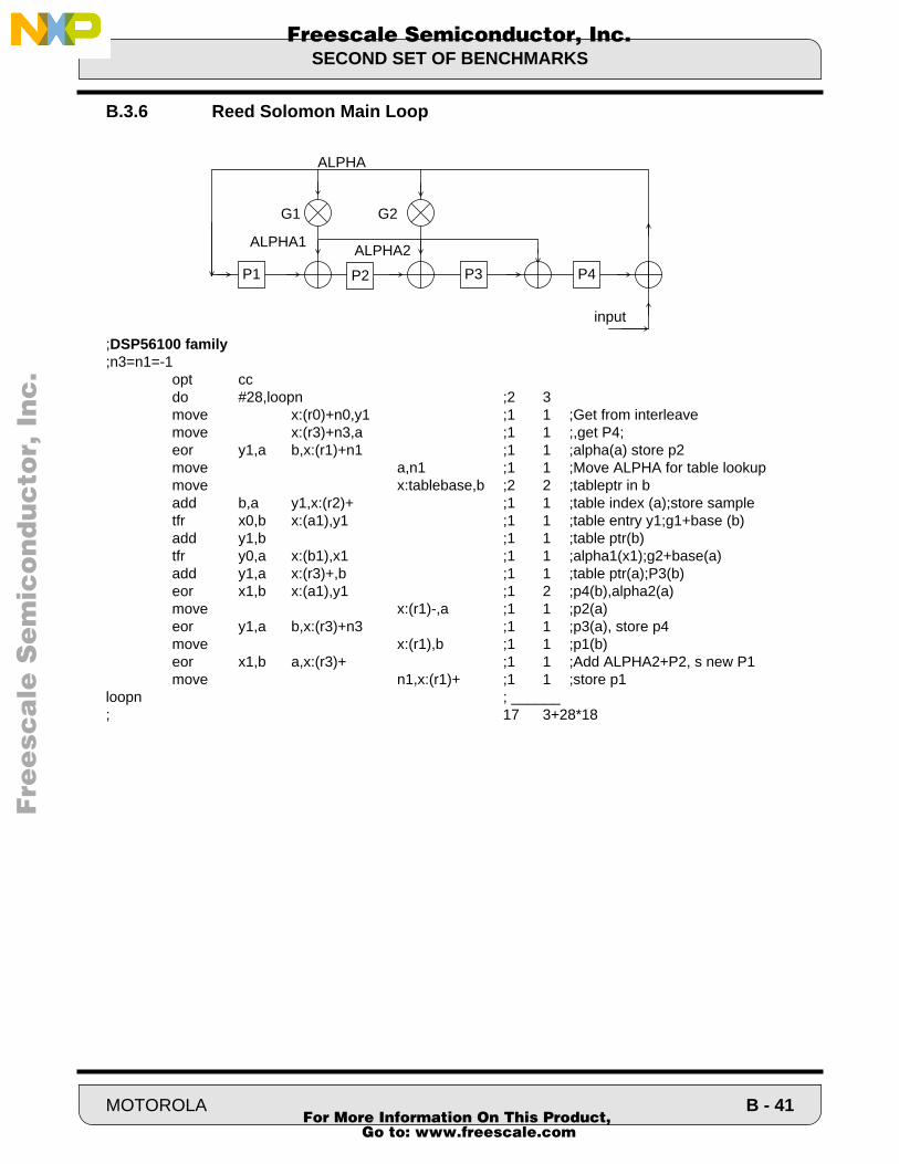
SECOND SET OF BENCHMARKS
F
ree
sca
le S
em
ico
nd
uc
tor,
I
Freescale Semiconductor, Inc.n
c..
.
B.3.6 Reed Solomon Main Loop
;DSP56100 family;n3=n1=-1
opt ccdo #28,loopn ;2 3move x:(r0)+n0,y1 ;1 1 ;Get from interleave move x:(r3)+n3,a ;1 1 ;,get P4;eor y1,a b,x:(r1)+n1 ;1 1 ;alpha(a) store p2move a,n1 ;1 1 ;Move ALPHA for table lookupmove x:tablebase,b ;2 2 ;tableptr in badd b,a y1,x:(r2)+ ;1 1 ;table index (a);store sampletfr x0,b x:(a1),y1 ;1 1 ;table entry y1;g1+base (b)add y1,b ;1 1 ;table ptr(b)tfr y0,a x:(b1),x1 ;1 1 ;alpha1(x1);g2+base(a)add y1,a x:(r3)+,b ;1 1 ;table ptr(a);P3(b)eor x1,b x:(a1),y1 ;1 2 ;p4(b),alpha2(a)move x:(r1)-,a ;1 1 ;p2(a)eor y1,a b,x:(r3)+n3 ;1 1 ;p3(a), store p4move x:(r1),b ;1 1 ;p1(b)eor x1,b a,x:(r3)+ ;1 1 ;Add ALPHA2+P2, s new P1move n1,x:(r1)+ ;1 1 ;store p1
loopn ; ______; 17 3+28*18
P1 P3
G1
input
P2
G2
P4
ALPHA1ALPHA2
ALPHA
MOTOROLA B - 41 For More Information On This Product,
Go to: www.freescale.com
SECOND SET OF BENCHMARKS
F
ree
sca
le S
em
ico
nd
uc
tor,
I
Freescale Semiconductor, Inc.n
c..
.
B.3.7 N Double Precision Real Multiplies
opt ccmove #AD,r0 ;2 2move #BD,r3 ;2 2move #c,r1 ;2 2
;move x:(r0)+,y0 x:(r3)+,x0 ;1 1do #N,end_loop ;2 3move x:(r0)+,y1 x:(r3)+,x1 ;1 1mpyuu x0,y0,a ;1 1move a0,x:(r1)+ ;1 1dmacsu x1,y0,a ;1 1macsu y1,x0,a ;1 1move a0,x:(r1)+ ;1 1dmacss y1,x1,a ;1 1move x:(r0)+,y0 x:(r3)+,x0 ;1 1move a0,x:(r1)+ ;1 1move a,x:(r1)+ ;1 1
end_loop ;______; 19 10*N+10
B.3.8 Double Precision Autocorrelation
; N: speech frame size; p: LPC order
;DSP56100 family
opt ccmove #cor,r1 ;2 2move #frame,r2 ;2 2do #lpc+1,_loop1 ;2 3move r2,r3 ;1 1clr b ;1 1move #frame,r0 ;2 2lua (r2)+,r2 ;1 2move lc,x1 ;1 1move #>N-(p+1),a ;2 2add x1,a x:(r0)+,y0 x:(r3)+,x0 ;1 1rep a ;1 2mac y0,x0,b x:(r0)+,y0 x:(r3)+,x0 ;1 1move b0,x:(r1)+ ;1 1move b1,x:(r1)+ ;1 1
_loop1 ;______
; 19 (p+1)2(N-p/2)+14(p+1) +5
;example: N=160 ; p=8;; DSP56100 family: 12,767 cycles at 25ns → 0.32ms (1.56% of 20ms);
B - 42 MOTOROLA For More Information On This Product,
Go to: www.freescale.com
MOTOROLA
SEMICONDUCTOR FAMILY MANUAL ADDENDUM
DSP56100
Order this document by:DSP56100FMAD/D
F
ree
sca
le S
em
ico
nd
uc
tor,
I
Freescale Semiconductor, Inc.n
c..
.
16-BIT DIGITAL SIGNAL PROCESSOR FAMILY
This document, containing changes, additional features, further explanations, and clarifications, is an addendum to the original document listed below:
Document Name: DSP56100 Family ManualOrder Number: DSP56100FM/ADRevision: 0
Change the following:
Page A-40 - For the BFCLR instruction, under “Explanation of Example:” change the phrase on the last portion of the last sentence to read “clears the carry bit C in CCR because not all these bits were clear, and then clears the bits.”
Page A-40 - For the BFCLR instruction, under C condition code bit definition listed under the title “For other destination operands:” change the definition to read:
C Set if all the bits specified by the mask are clear.Clear if not all the bits specified by the mask are clear.
Pages A-48 (Bcc instruction), A-50 (BRA instruction), A-54 (BScc instruction), and A-56 (BSR instruction) under “Restrictions” remove the last item (“ Not allowed between addresses P:$0 and P:$40.”).
Page A-147 - For MOVE(C) instructions using the instruction format:
MOVE(C) X:<A1,B1>,D MOVE(C) S,X:<A1,B1>
change the box that appears as:
to the following:
ea Z
(A1) 0
(B1) 1
ea Z
(A1) 1
(B1) 0
©1996 MOTOROLA, INC.
For More Information On This Product,
Go to: www.freescale.com

F
ree
sca
le S
em
ico
nd
uc
tor,
I
Freescale Semiconductor, Inc.n
c..
.
Motorola reserves the right to make changes without further notice to any products herein. Motorola makes nowarranty, representation or guarantee regarding the suitability of its products for any particular purpose, nor doesMotorola assume any liability arising out of the application or use of any product or circuit, and specificallydisclaims any and all liability, including without limitation consequential or incidental damages. “Typical”parameters can and do vary in different applications. All operating parameters, including “Typical”, must bevalidated for each customer application by customer’s technical experts. Motorola does not convey any licenseunder its patent rights nor the rights of others. Motorola products are not designed, intended, or authorized for useas components in systems intended for surgical implant into the body, or other applications intended to support orsustain life, or for any other application in which the failure of the Motorola product could create a situation wherepersonal injury or death may occur. Should Buyer purchase or use Motorola products for any such unintended orunauthorized application, Buyer shall indemnify and hold Motorola and its officers, employees, subsidiaries,affiliates, and distributors harmless against all claims, costs, damages, and expenses, and reasonable attorneyfees arising out of, directly or indirectly, any claim of personal injury or death associated with such unintended orunauthorized use, even if such claim alleges that Motorola was negligent regarding the design or manufacture ofthe part.
OnCE, Motorola, and are registered trademarks of Motorola, Inc.
USA/Europe:Motorola Literature DistributionP.O. Box 20912Phoenix, Arizona 850361 (800) 441-2447
MFAX:[email protected]
Hong Kong:Motorola Semiconductors H.K. Ltd.8B Tai Ping Industrial Park51 Ting Kok RoadTai Po, N.T., Hong Kong852-2662928
Japan:Nippon Motorola Ltd.Tatsumi-SPD-JLDCToshikatsu Otsuki6F Seibu-Butsuryu-Center3-14-2 Tatsumi Koto-KuTokyo 135, Japan03-3521-8315
How to reach us:
Internet:http://motserv.indirect.com/dsp/DSPhome.html
Pages A-153, A-155, A-157, and A-159 - In the table that defines the value of W, add a second line as shown below:
Page A-232 - Change Table A-9 to the following:
Reg. W
read S 0
write D 1
Table A-9 MOVEM Timing Summary
MOVEM Operation + mvm Cycles Comments
Register ↔ P MemoryX Memory ↔ P Memory
4 + ea + ap4 + ea + ax + ap
TOUCHTONE (602) 244-6609
For More Information On This Product,
Go to: www.freescale.com