Course Objectives and outcomes for LD of Experiments Expt No. Experiment 1 Verify the truth table of...
44
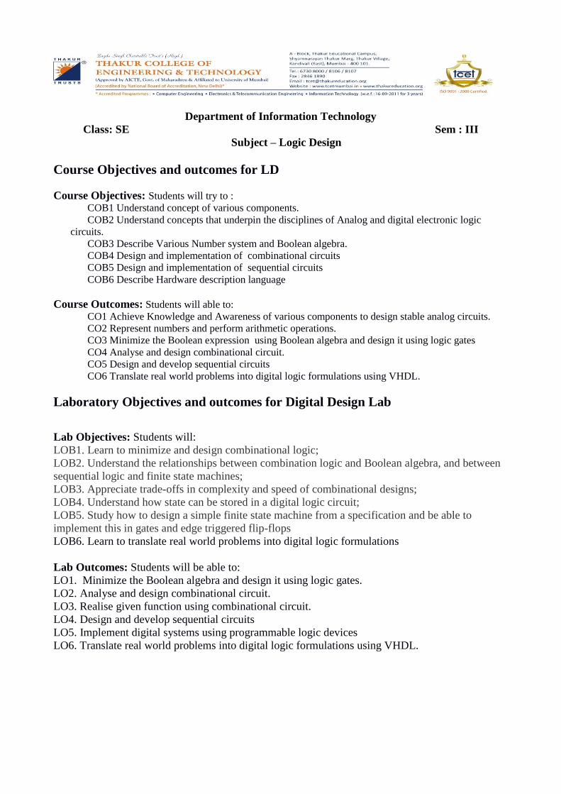
Department of Information Technology Class: SE Sem : III Subject – Logic Design Course Objectives and outcomes for LD Course Objectives: Students will try to : COB1 Understand concept of various components. COB2 Understand concepts that underpin the disciplines of Analog and digital electronic logic circuits. COB3 Describe Various Number system and Boolean algebra. COB4 Design and implementation of combinational circuits COB5 Design and implementation of sequential circuits COB6 Describe Hardware description language Course Outcomes: Students will able to: CO1 Achieve Knowledge and Awareness of various components to design stable analog circuits. CO2 Represent numbers and perform arithmetic operations. CO3 Minimize the Boolean expression using Boolean algebra and design it using logic gates CO4 Analyse and design combinational circuit. CO5 Design and develop sequential circuits CO6 Translate real world problems into digital logic formulations using VHDL. Laboratory Objectives and outcomes for Digital Design Lab Lab Objectives: Students will: LOB1. Learn to minimize and design combinational logic; LOB2. Understand the relationships between combination logic and Boolean algebra, and between sequential logic and finite state machines; LOB3. Appreciate trade-offs in complexity and speed of combinational designs; LOB4. Understand how state can be stored in a digital logic circuit; LOB5. Study how to design a simple finite state machine from a specification and be able to implement this in gates and edge triggered flip-flops LOB6. Learn to translate real world problems into digital logic formulations Lab Outcomes: Students will be able to: LO1. Minimize the Boolean algebra and design it using logic gates. LO2. Analyse and design combinational circuit. LO3. Realise given function using combinational circuit. LO4. Design and develop sequential circuits LO5. Implement digital systems using programmable logic devices LO6. Translate real world problems into digital logic formulations using VHDL.
Transcript of Course Objectives and outcomes for LD of Experiments Expt No. Experiment 1 Verify the truth table of...
Department of Information Technology
Class: SE Sem : III
Subject – Logic Design
Course Objectives and outcomes for LD
Course Objectives: Students will try to :
COB1 Understand concept of various components.
COB2 Understand concepts that underpin the disciplines of Analog and digital electronic logic
circuits.
COB3 Describe Various Number system and Boolean algebra.
COB4 Design and implementation of combinational circuits
COB5 Design and implementation of sequential circuits
COB6 Describe Hardware description language
Course Outcomes: Students will able to:
CO1 Achieve Knowledge and Awareness of various components to design stable analog circuits.
CO2 Represent numbers and perform arithmetic operations.
CO3 Minimize the Boolean expression using Boolean algebra and design it using logic gates
CO4 Analyse and design combinational circuit.
CO5 Design and develop sequential circuits
CO6 Translate real world problems into digital logic formulations using VHDL.
Laboratory Objectives and outcomes for Digital Design Lab
Lab Objectives: Students will:
LOB1. Learn to minimize and design combinational logic;
LOB2. Understand the relationships between combination logic and Boolean algebra, and between
sequential logic and finite state machines;
LOB3. Appreciate trade-offs in complexity and speed of combinational designs;
LOB4. Understand how state can be stored in a digital logic circuit;
LOB5. Study how to design a simple finite state machine from a specification and be able to
implement this in gates and edge triggered flip-flops
LOB6. Learn to translate real world problems into digital logic formulations
Lab Outcomes: Students will be able to:
LO1. Minimize the Boolean algebra and design it using logic gates.
LO2. Analyse and design combinational circuit.
LO3. Realise given function using combinational circuit.
LO4. Design and develop sequential circuits
LO5. Implement digital systems using programmable logic devices
LO6. Translate real world problems into digital logic formulations using VHDL.
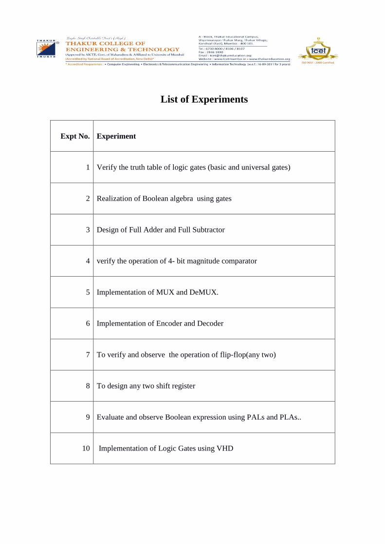
List of Experiments
Expt No. Experiment
1 Verify the truth table of logic gates (basic and universal gates)
2 Realization of Boolean algebra using gates
3 Design of Full Adder and Full Subtractor
4 verify the operation of 4- bit magnitude comparator
5 Implementation of MUX and DeMUX.
6 Implementation of Encoder and Decoder
7 To verify and observe the operation of flip-flop(any two)
8 To design any two shift register
9 Evaluate and observe Boolean expression using PALs and PLAs..
10 Implementation of Logic Gates using VHD
PRECAUTION
1. All the IC’s should be checked before use the apparatus.
2. All LED’s should be checked.
3. All connections should be tight.
4. Always connect GROUND first and then Vcc
5. The circuit should be off before change the connections.
6. After completing the experiment switch off the supply to apparatus, wind up the circuits.
7. Keep all apparatus properly before leaving the place.
Experiment Write Ups
AIM: Verify the truth table of logic gates (basic and universal gates)
LEARNING OBJECTIVES:
LOB1
TOOLS/SOFTWARE REQUIRED:
Logic gates (IC) trainer kit.
Connecting patch chords.
IC 7400, IC 7402, IC 7404, IC 7406, IC 7408, IC 7432, IC 7486
RELATED THEORY:
The basic logic gates are the building blocks of more complex logic circuits. These logic gates
perform the basic Boolean functions, such as AND, OR, NAND, NOR, Inversion, Exclusive-OR,
Exclusive-NOR. Fig. below shows the circuit symbol, Boolean function, and truth. It is seen from
the Fig that each gate has one or two binary inputs, A and B, and one binary output, C. The small
circle on the output of the circuit symbols designates the logic complement. The AND, OR, NAND,
and NOR gates can be extended to have more than two inputs. A gate can be extended to have
multiple inputs if the binary operation it represents is commutative and associative.
These basic logic gates are implemented as small-scale integrated circuits (SSICs) or as part of
more complex medium scale (MSI) or very large-scale (VLSI) integrated circuits. Digital IC gates
are classified not only by their logic operation, but also the specific logic-circuit family to which
they belong. Each logic family has its own basic electronic circuit upon which more complex digital
circuits and functions are developed. The following logic families are the most frequently used.
TTL : Transistor-transistor logic
ECL : Emitter-coupled logic
MOS : Metal-oxide semiconductor
CMOS: Complementary metal-oxide semiconductor
TTL and ECL are based upon bipolar transistors. TTL has a well established popular among logic
families. ECL is used only in systems requiring high-speed operation. MOS and CMOS, are based
on field effect transistors. They are widely used in large scale integrated circuits because of their
high component density and relatively low power consumption.
CMOS logic consumes far less power than MOS logic. There are various commercial integrated
circuit chips available. TTL ICs are usually distinguished by numerical designation as the 5400 and
7400 series.
ICs are classified by:
a. Logic Families
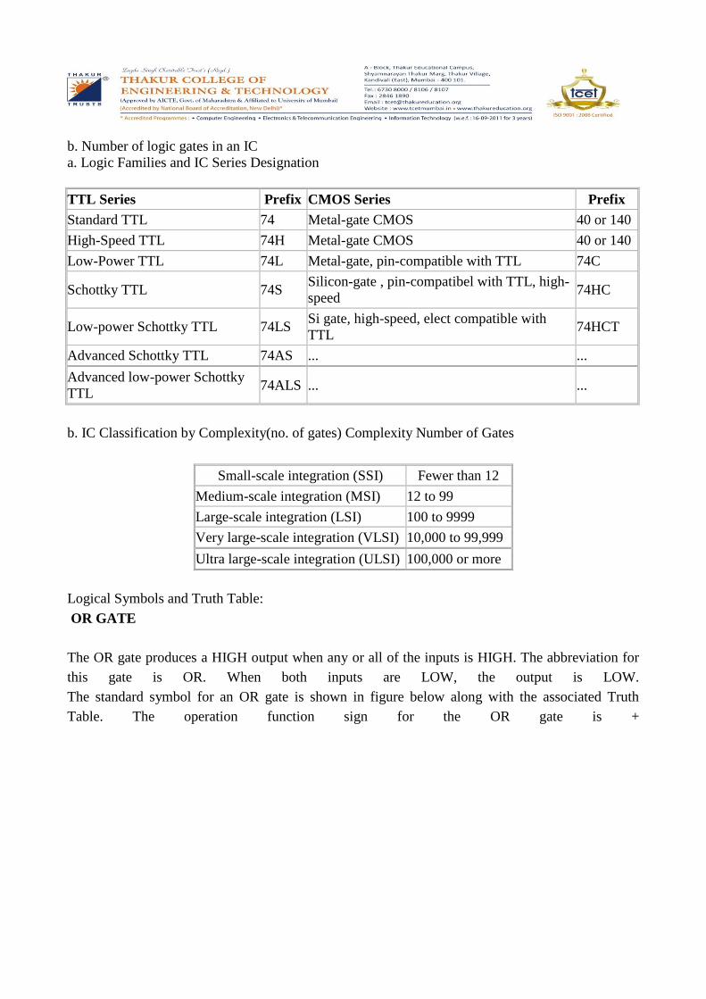
b. Number of logic gates in an IC
a. Logic Families and IC Series Designation
TTL Series Prefix CMOS Series Prefix
Standard TTL 74 Metal-gate CMOS 40 or 140
High-Speed TTL 74H Metal-gate CMOS 40 or 140
Low-Power TTL 74L Metal-gate, pin-compatible with TTL 74C
Schottky TTL 74S Silicon-gate , pin-compatibel with TTL, high-
speed 74HC
Low-power Schottky TTL 74LS Si gate, high-speed, elect compatible with
TTL 74HCT
Advanced Schottky TTL 74AS ... ...
Advanced low-power Schottky
TTL 74ALS ... ...
b. IC Classification by Complexity(no. of gates) Complexity Number of Gates
Small-scale integration (SSI) Fewer than 12
Medium-scale integration (MSI) 12 to 99
Large-scale integration (LSI) 100 to 9999
Very large-scale integration (VLSI) 10,000 to 99,999
Ultra large-scale integration (ULSI) 100,000 or more
Logical Symbols and Truth Table:
OR GATE
The OR gate produces a HIGH output when any or all of the inputs is HIGH. The abbreviation for
this gate is OR. When both inputs are LOW, the output is LOW.
The standard symbol for an OR gate is shown in figure below along with the associated Truth
Table. The operation function sign for the OR gate is +
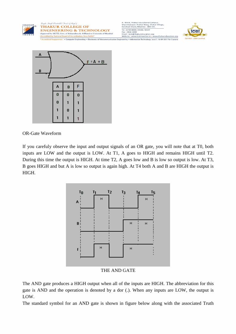
OR-Gate Waveform
If you carefuly observe the input and output signals of an OR gate, you will note that at T0, both
inputs are LOW and the output is LOW. At T1, A goes to HIGH and remains HIGH until T2.
During this time the output is HIGH. At time T2, A goes low and B is low so output is low. At T3,
B goes HIGH and but A is low so output is again high. At T4 both A and B are HIGH the output is
HIGH.
THE AND GATE
The AND gate produces a HIGH output when all of the inputs are HIGH. The abbreviation for this
gate is AND and the operation is denoted by a dor (.). When any inputs are LOW, the output is
LOW.
The standard symbol for an AND gate is shown in figure below along with the associated Truth
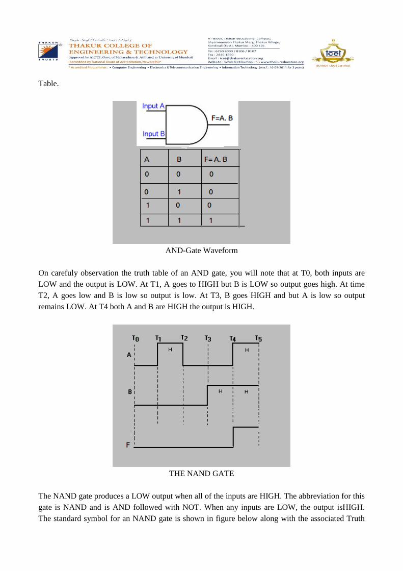
Table.
AND-Gate Waveform
On carefuly observation the truth table of an AND gate, you will note that at T0, both inputs are
LOW and the output is LOW. At T1, A goes to HIGH but B is LOW so output goes high. At time
T2, A goes low and B is low so output is low. At T3, B goes HIGH and but A is low so output
remains LOW. At T4 both A and B are HIGH the output is HIGH.
THE NAND GATE
The NAND gate produces a LOW output when all of the inputs are HIGH. The abbreviation for this
gate is NAND and is AND followed with NOT. When any inputs are LOW, the output isHIGH.
The standard symbol for an NAND gate is shown in figure below along with the associated Truth
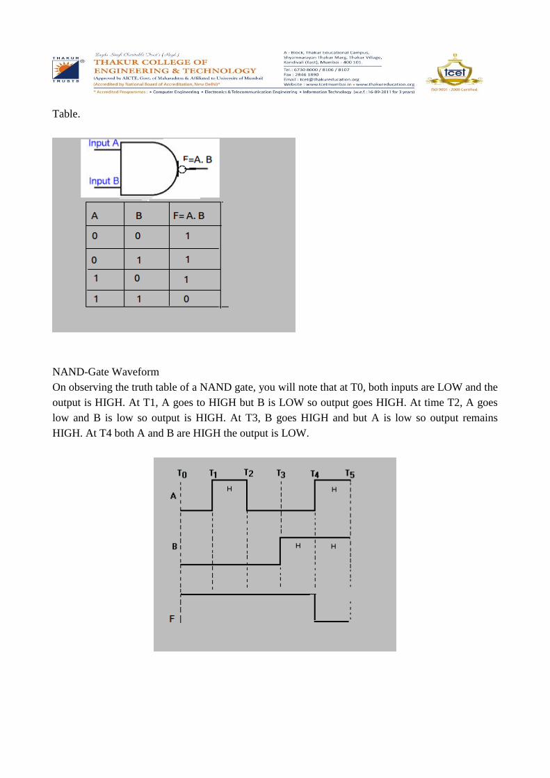
Table.
NAND-Gate Waveform
On observing the truth table of a NAND gate, you will note that at T0, both inputs are LOW and the
output is HIGH. At T1, A goes to HIGH but B is LOW so output goes HIGH. At time T2, A goes
low and B is low so output is HIGH. At T3, B goes HIGH and but A is low so output remains
HIGH. At T4 both A and B are HIGH the output is LOW.
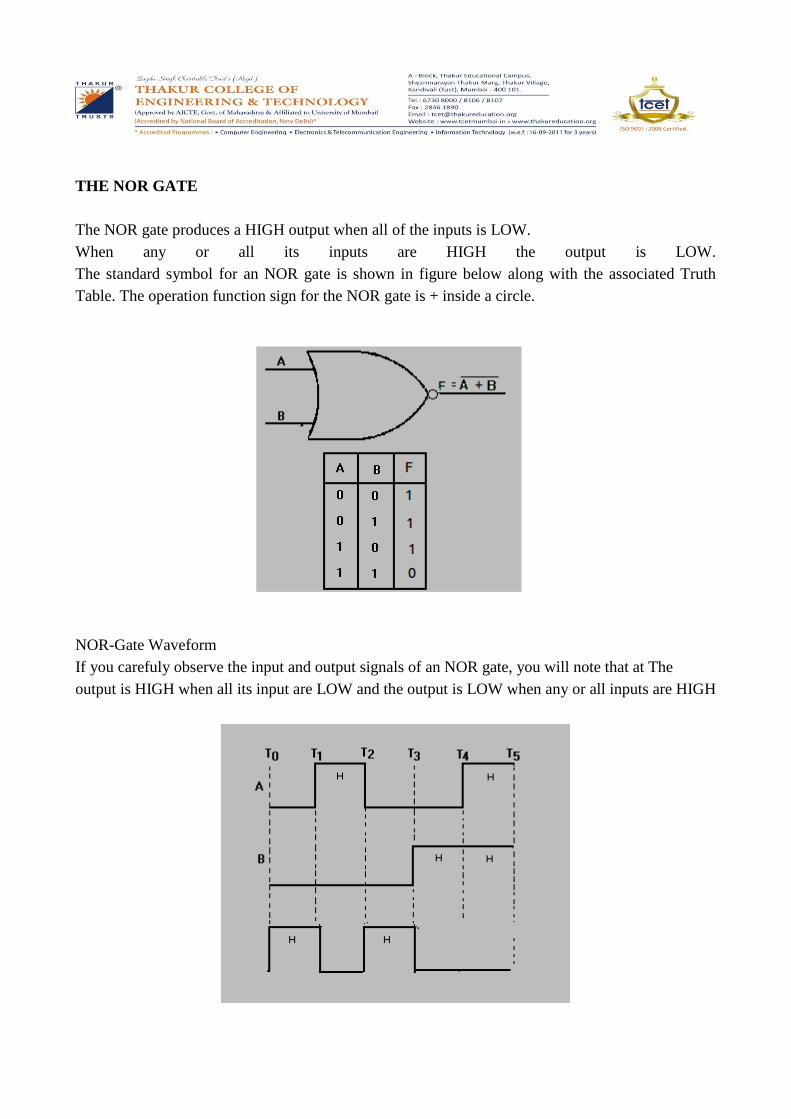
THE NOR GATE
The NOR gate produces a HIGH output when all of the inputs is LOW.
When any or all its inputs are HIGH the output is LOW.
The standard symbol for an NOR gate is shown in figure below along with the associated Truth
Table. The operation function sign for the NOR gate is + inside a circle.
NOR-Gate Waveform
If you carefuly observe the input and output signals of an NOR gate, you will note that at The
output is HIGH when all its input are LOW and the output is LOW when any or all inputs are HIGH
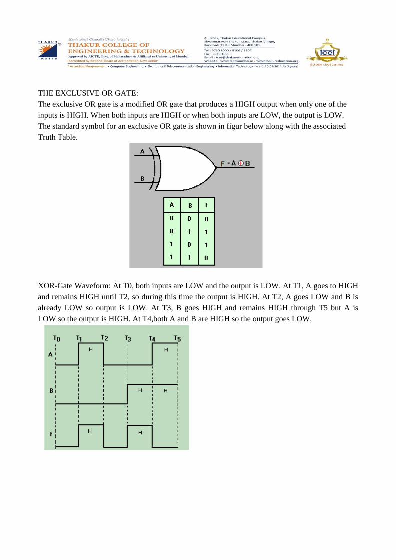
THE EXCLUSIVE OR GATE:
The exclusive OR gate is a modified OR gate that produces a HIGH output when only one of the
inputs is HIGH. When both inputs are HIGH or when both inputs are LOW, the output is LOW.
The standard symbol for an exclusive OR gate is shown in figur below along with the associated
Truth Table.
XOR-Gate Waveform: At T0, both inputs are LOW and the output is LOW. At T1, A goes to HIGH
and remains HIGH until T2, so during this time the output is HIGH. At T2, A goes LOW and B is
already LOW so output is LOW. At T3, B goes HIGH and remains HIGH through T5 but A is
LOW so the output is HIGH. At T4,both A and B are HIGH so the output goes LOW,
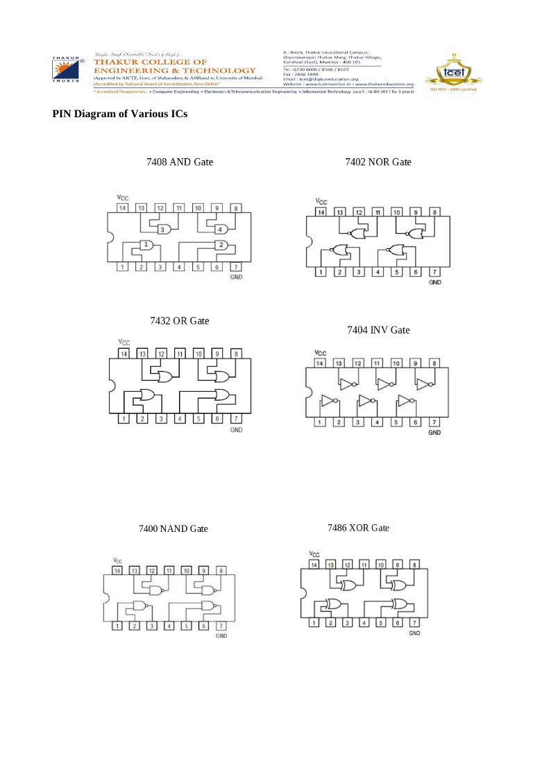
PIN Diagram of Various ICs

PROCEDURE:
1. Check the components for their working.
2. Insert the appropriate IC into the IC base.
3. Make connections as shown in the circuit diagram.
4. Provide the input data via the input switches and observe the output on output LEDs
RESULT/ VERIFICATION:
Verify the behaviour of the different gates with the truth table
CONCLUSION:
Thus verified the truth table of logic basic and universal gates
LEARNING OUTCOMES:
LO1
COURSE OUTCOMES:
a)CO1
IMPORTANT QUESTIONS
1. What is a logic gate?
2. What are universal gates?
3. What are Basic Gates
4. Which of the two input logic gate can be used to implement an inverter circuit?
5. Which are the logic gates whose all output entries are logic 1 except for one entry there is
logic 0?
6. TTL operates at (power rating)
7. When the output of a NOR gate is high?
8. Why NAND & NOR gates are called universal gates?
9. Realize the EX – OR gates using minimum number of NAND gates.
10. Give the truth table for EX-NOR and realize using NAND gates?
AIM: Realization of Boolean algebra using gates
LEARNING OBJECTIVES:
LOB1, LOB2
TOOLS/SOFTWARE REQUIRED:
Logic gates (IC) trainer kit.
Connecting patch chords.
IC 7400, IC 7402, IC 7404, IC 7406, IC 7408, IC 7432, IC 7486
RELATED THEORY:
Canonical Forms (Normal Forms): Any Boolean function can be written in disjunctive normal form
(sum of min-terms) or conjunctive normal form (product of max-terms). A Boolean function can be
represented by a Karnaugh map in which each cell corresponds to a minterm. The cells are arranged
in such a way that any two immediately adjacent cells correspond to two minterms of distance 1.
There is more than one way to construct a map with this property.
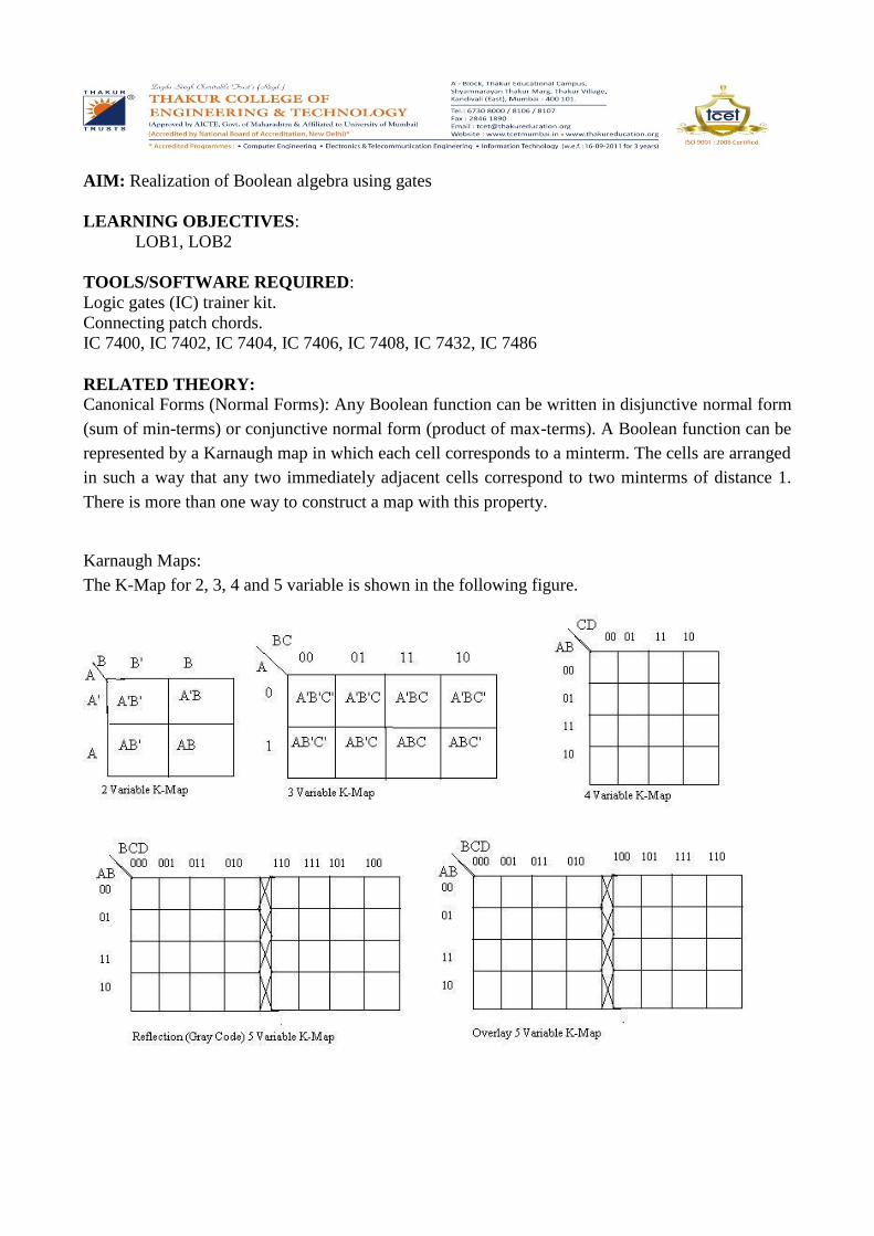
Karnaugh Maps:
The K-Map for 2, 3, 4 and 5 variable is shown in the following figure.
Realization of SOP Boolean expression:
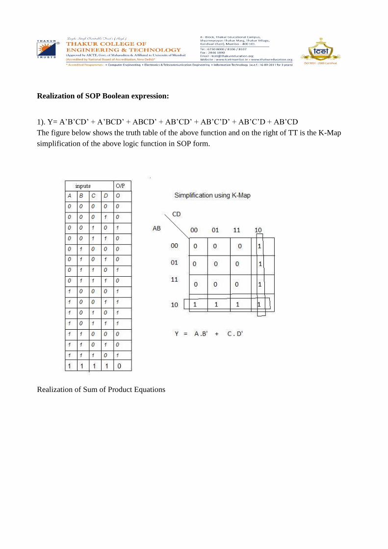
1). Y= A’B’CD’ + A’BCD’ + ABCD’ + AB’CD’ + AB’C’D’ + AB’C’D + AB’CD
The figure below shows the truth table of the above function and on the right of TT is the K-Map
simplification of the above logic function in SOP form.
Realization of Sum of Product Equations
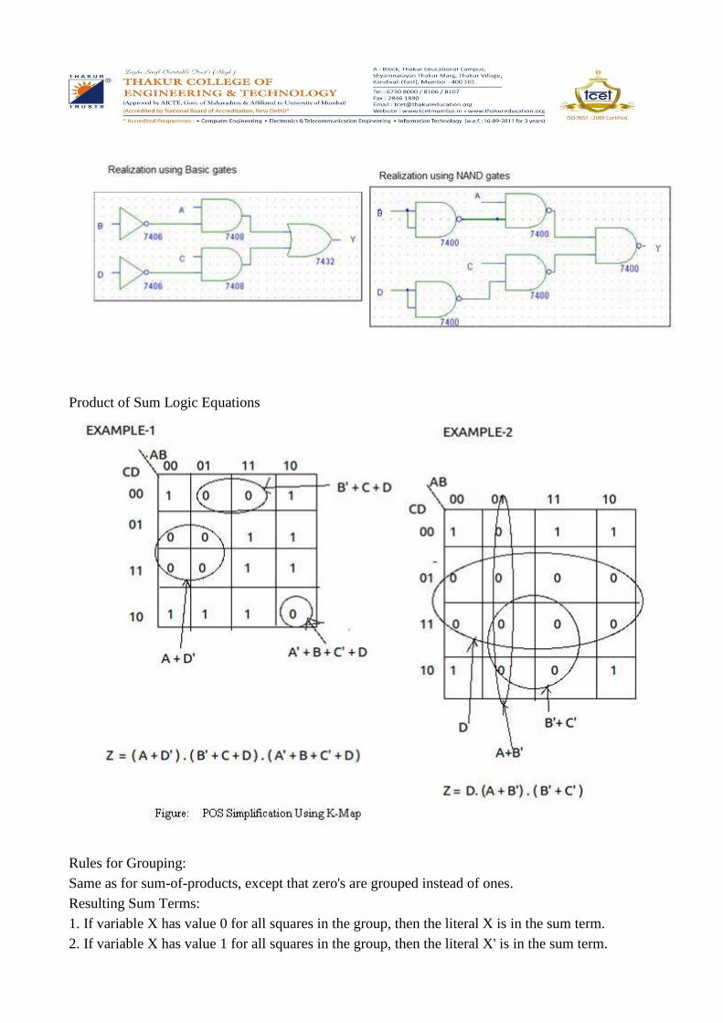
Product of Sum Logic Equations
Rules for Grouping:
Same as for sum-of-products, except that zero's are grouped instead of ones.
Resulting Sum Terms:
1. If variable X has value 0 for all squares in the group, then the literal X is in the sum term.
2. If variable X has value 1 for all squares in the group, then the literal X' is in the sum term.
3. If variable X has value 0 for some squares in the group and value 1 for the others, then that
variable does not appear in the sum term.
Prime Implicate: Maximal grouping of zeros
b>Verification:
Result:- Hence, given Boolean Expression is implemented by the Logic Gates.
SOP Equation
1). Y= AB' + CD'
POS equation
(i) D.(A+B').(B'+C')
(ii) (A+D'). (B'+C+D). (A'+B+C’+D)
PROCEDURE:
RESULTS & DISCUSSION:
CONCLUSION: Thus Realized of Boolean algebra using gates
LEARNING OUTCOMES:
LO1, LO2
COURSE OUTCOMES:
a)CO2
b) CO3
IMPORTANT QUESTIONS:-
1) What is a combinational circuit?
2) What is a sequential circuit?
3) What are the various methods of simplifying the Boolean Function.
4) What do you mean by minterm?
5) What do you mean by maxterm?
1) Convert the expression Y=AC’ + AB+AC into SOP form.
2) Convert the POS expression Y= (A+B) (B+C) (A+C) expression into canonical POS
3) Define POS.
4) Define SOP.
5) Define canonical form representation of Boolean function.
AIM: Design of Full Adder and Full Subtractor
LEARNING OBJECTIVES:
LOB1, LOB2, LOB3
TOOLS/SOFTWARE REQUIRED:
Logic gates (IC) trainer kit.
Connecting patch chords.
IC 7400, IC 7402, IC 7404, IC 7406, IC 7408, IC 7432, IC 7486
RELATED THEORY:
Half Adder:
A half adder is a combinational circuit that performs the sum of two binary digits (A, B) to
give a maximum of two binary outputs namely the sum(S) and the carry(C). Carry is the higher
order bit and the sum is the lower order bit of the output.Functional Table of the Half-Adder is
given below:
The Boolean expression for the sum(S) and carry(C) of half adder is,
SUM = AB' + A'B; which is same as XOR of A and B
CARRY= AB
HA Using NAND gates
Logical equation for Sum = AB' + A'B; can be converted into NAND for by taking the double
complement of the equation as:
(Sum')' = { ( AB' + A'B)'}' and Carry C''= {(AB)'}' = {(AB')' . (A'B)'}'
LOGIC-CIRCUIT
FULL ADDER:
A full adder is a combinational circuit that performs the sum of three binary digits (A, B, Cin) to
give a maximum of two binary outputs namely the sum(S) and the carry- out (Cout).The full adder
becomes necessary when a carry input must be added to the two binary digits to obtain the correct
sum. A half adder has no input for carries from previous circuits.
The Boolean expression for the sum (S) and carry-out (Cout) of full adder is,
SUM = A'B'C + A'BC' + AB'C' + ABC
Cout = A'BC + AB'C + ABC' + ABC
SIMPLIFICATION OF LOGIC EQUATIONS SUM = A'B'C + A'BC' + AB'C' + ABC
= A’(B’C+BC’) + A(B’C’+BC)
=A XOR B XOR C
Cout = A'BC + AB'C + ABC' + ABC
= A'BC + ABC+ AB'C + ABC'
= BC(A+A’) + A(B’C+BC)
= BC + A(B XOR C)
LOGIC DIAGRAM
The full adder drawn above can be visualized as a combination of two half adders. It uses two XOR
gates, the output of 1st XOR gate (i.e. SUM A+B) is taken as input to 2nd XOR gate and the other
is the third input( usually the Cin), the outputs of the AND gates which are nothing but the carry of
HA are ORed together. The FA drawn as a combination of two HA is shown below.
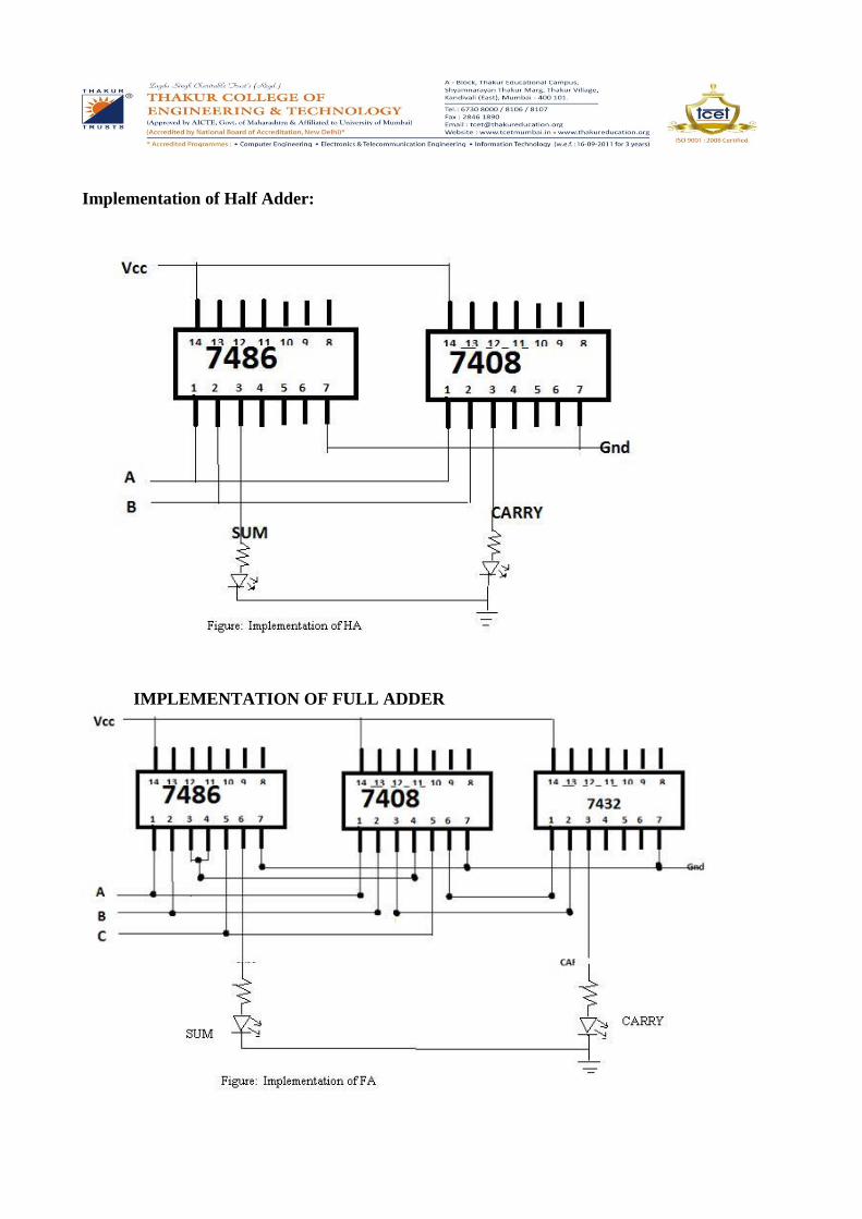
Implementation of Half Adder:
IMPLEMENTATION OF FULL ADDER
FULL SUBTRACTOR :
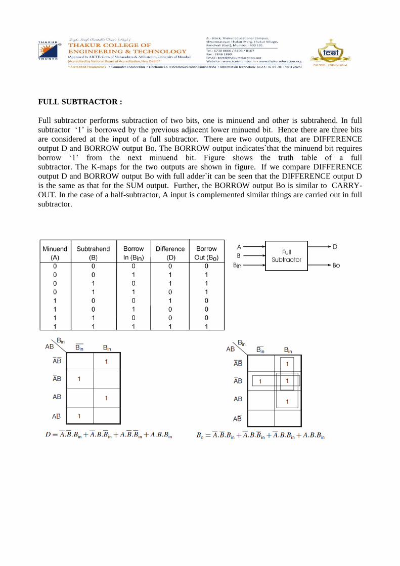
Full subtractor performs subtraction of two bits, one is minuend and other is subtrahend. In full
subtractor ‘1’ is borrowed by the previous adjacent lower minuend bit. Hence there are three bits
are considered at the input of a full subtractor. There are two outputs, that are DIFFERENCE
output D and BORROW output Bo. The BORROW output indicates`that the minuend bit requires
borrow ‘1’ from the next minuend bit. Figure shows the truth table of a full
subtractor. The K-maps for the two outputs are shown in figure. If we compare DIFFERENCE
output D and BORROW output Bo with full adder`it can be seen that the DIFFERENCE output D
is the same as that for the SUM output. Further, the BORROW output Bo is similar to CARRY-
OUT. In the case of a half-subtractor, A input is complemented similar things are carried out in full
subtractor.
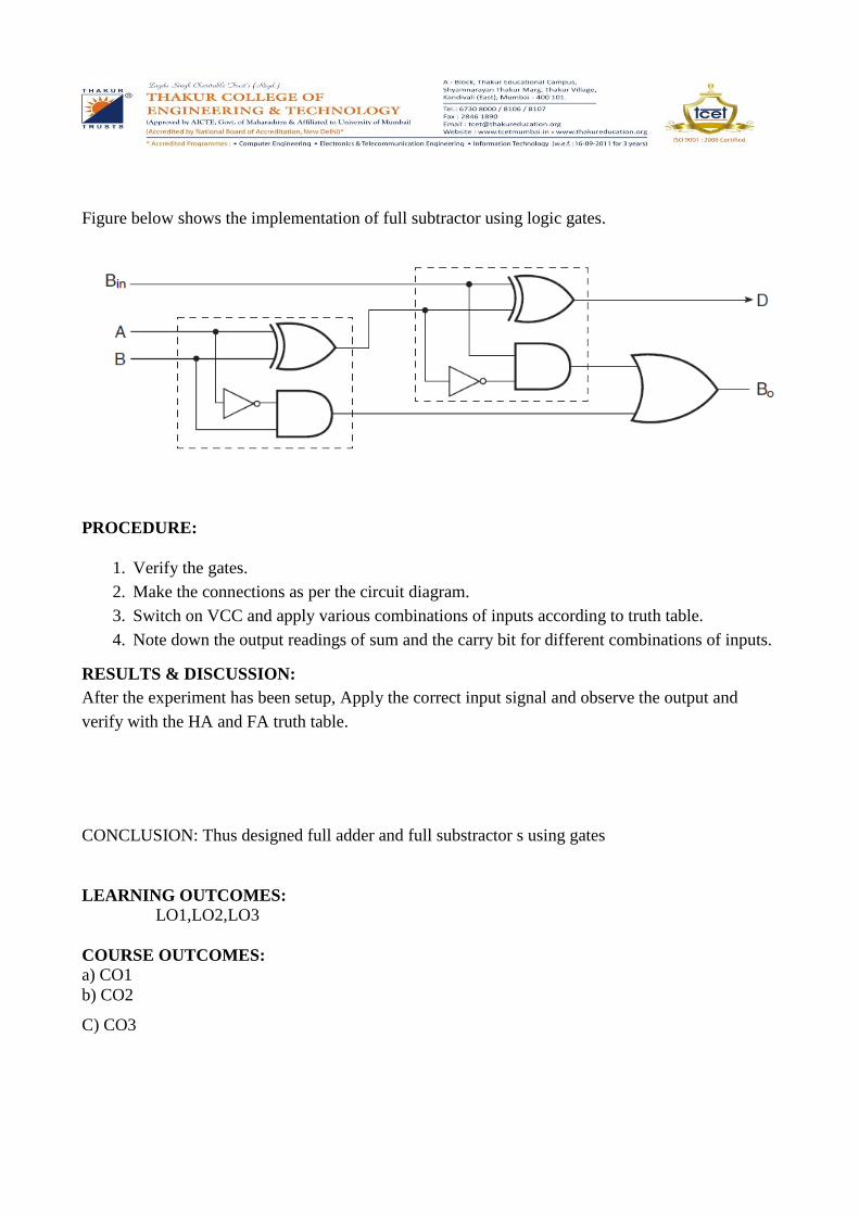
Figure below shows the implementation of full subtractor using logic gates.
PROCEDURE:
1. Verify the gates.
2. Make the connections as per the circuit diagram.
3. Switch on VCC and apply various combinations of inputs according to truth table.
4. Note down the output readings of sum and the carry bit for different combinations of inputs.
RESULTS & DISCUSSION:
After the experiment has been setup, Apply the correct input signal and observe the output and
verify with the HA and FA truth table.
CONCLUSION: Thus designed full adder and full substractor s using gates
LEARNING OUTCOMES:
LO1,LO2,LO3
COURSE OUTCOMES:
a) CO1
b) CO2
C) CO3
AIM: verify the operation of 4- bit magnitude comparator
LEARNING OBJECTIVES:
LOB1, LOB2, LOB3
TOOLS/SOFTWARE REQUIRED:
Logic gates (IC) trainer kit.
Connecting patch chords.
IC 7400, IC 7411, IC 7408, IC 7485, IC 7486
RELATED THEORY:
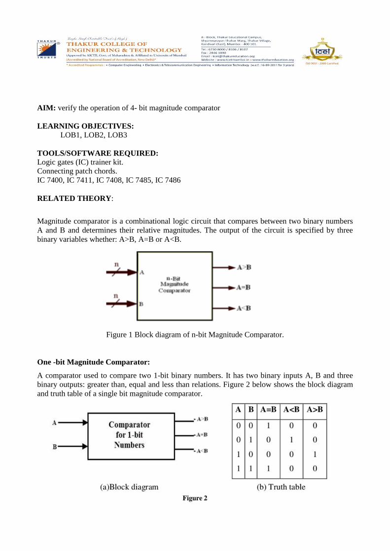
Magnitude comparator is a combinational logic circuit that compares between two binary numbers
A and B and determines their relative magnitudes. The output of the circuit is specified by three
binary variables whether: A>B, A=B or A<B.
Figure 1 Block diagram of n-bit Magnitude Comparator.
One -bit Magnitude Comparator:
A comparator used to compare two 1-bit binary numbers. It has two binary inputs A, B and three
binary outputs: greater than, equal and less than relations. Figure 2 below shows the block diagram
and truth table of a single bit magnitude comparator.
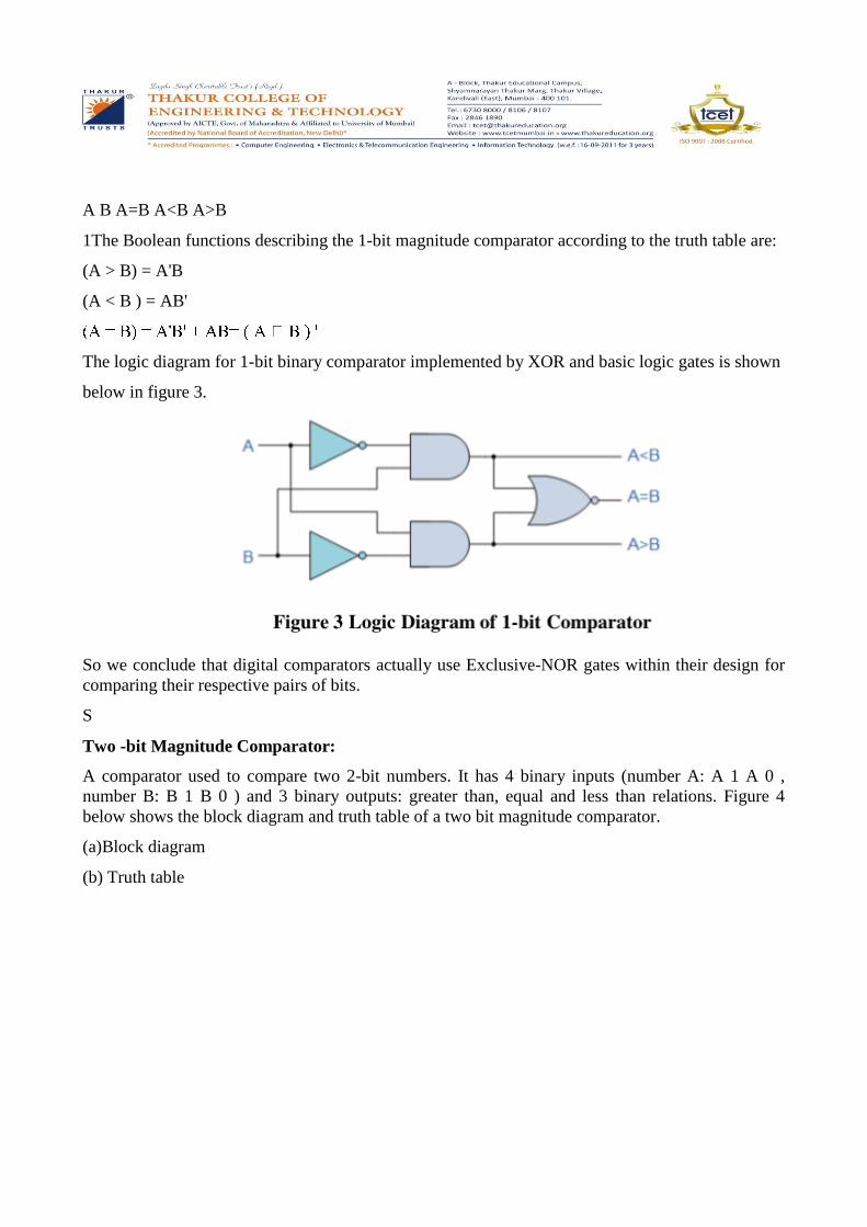
A B A=B A<B A>B
1The Boolean functions describing the 1-bit magnitude comparator according to the truth table are:
(A > B) = A'B
(A < B ) = AB'
The logic diagram for 1-bit binary comparator implemented by XOR and basic logic gates is shown
below in figure 3.
So we conclude that digital comparators actually use Exclusive-NOR gates within their design for
comparing their respective pairs of bits.
S
Two -bit Magnitude Comparator:
A comparator used to compare two 2-bit numbers. It has 4 binary inputs (number A: A 1 A 0 ,
number B: B 1 B 0 ) and 3 binary outputs: greater than, equal and less than relations. Figure 4
below shows the block diagram and truth table of a two bit magnitude comparator.
(a)Block diagram
(b) Truth table
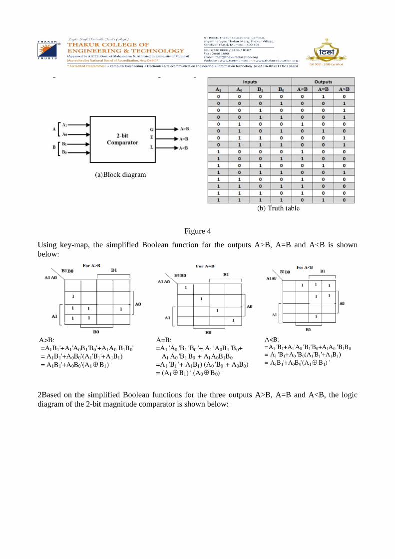
Figure 4
Using key-map, the simplified Boolean function for the outputs A>B, A=B and A<B is shown
below:
2Based on the simplified Boolean functions for the three outputs A>B, A=B and A<B, the logic
diagram of the 2-bit magnitude comparator is shown below:
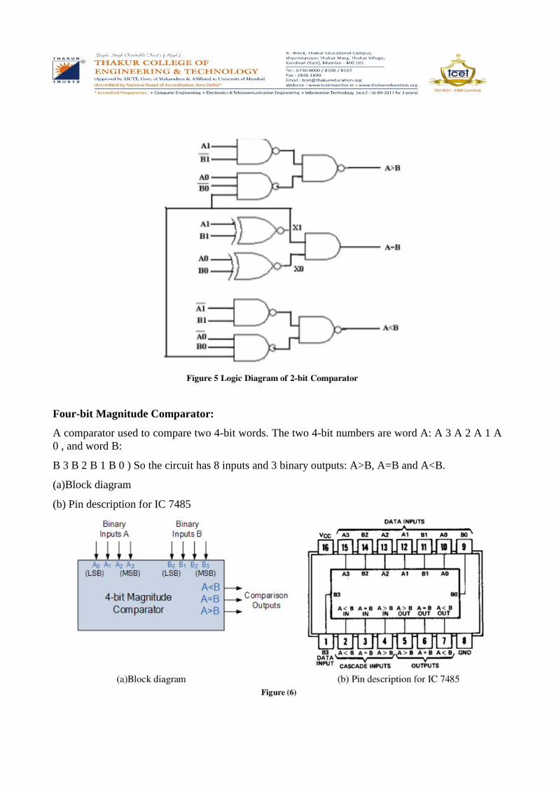
Four-bit Magnitude Comparator:
A comparator used to compare two 4-bit words. The two 4-bit numbers are word A: A 3 A 2 A 1 A
0 , and word B:
B 3 B 2 B 1 B 0 ) So the circuit has 8 inputs and 3 binary outputs: A>B, A=B and A<B.
(a)Block diagram
(b) Pin description for IC 7485
Figure 6 shows the block diagram and pin configuration of IC 7485 for 4-bit magnitude comparator.
Three inputs are available for cascading comparators.
This comparator generates an output of 1 at one of three comparison outputs such that:
rd A is smaller than word B; A<B output is “1”,
3This IC can be used to compare two 4-bit binary words by grounding I (A>B), I (A<B) and I
(A=B) connector input to Vcc terminal.
How 4-bit comparator it works?
Equality:
Word A equal word B iff: A 3 =B 3 , A 2 =B 2 , A 1 =B 1 , A 0 =B 0.
Inequality:
are equal, and if A1 = 1, and B1 = 0, then A>B. Or
then A > B.
and B2 = 1, then A < B. Or
then A < B.
PROCEDURE:
1. Connections are made as per circuit diagram.
2. Verify the truth table.
3. Also connect Vcc and Ground then performed experiment.
Precautions:-
a. All ICs should be checked before starting the experiment.
b. All the connection should be tight.
c. Always connect ground first and then connect Vcc.
d. Suitable type wire should be used for different types of circuit.
e. The kit should be off before change the connections.
f. After completed the experiments switch off the supply of the apparatus

CONCLUSION: Thus verified 4 bit magnitude comparator.
LEARNING OUTCOMES:
LO1,LO2,LO3
COURSE OUTCOMES:
a) CO1
b) CO2
AIM: Implementation of MUX and De-MUX using basic logic gates
LEARNING OBJECTIVES:
LOB1, LOB2, LOB3
TOOLS/SOFTWARE REQUIRED: -
Digital trainer kit, AND-7411, OR-7432, NOT-7404 Gate IC, Connecting wires
RELATED THEORY:
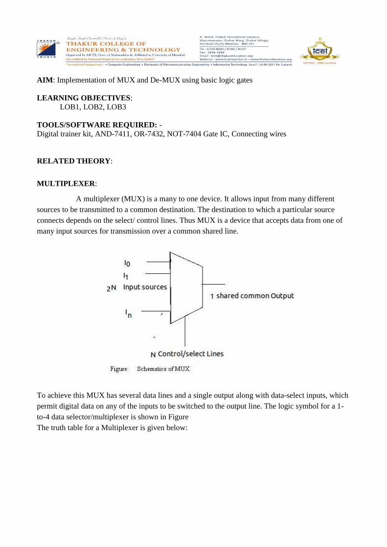
MULTIPLEXER:
A multiplexer (MUX) is a many to one device. It allows input from many different
sources to be transmitted to a common destination. The destination to which a particular source
connects depends on the select/ control lines. Thus MUX is a device that accepts data from one of
many input sources for transmission over a common shared line.
To achieve this MUX has several data lines and a single output along with data-select inputs, which
permit digital data on any of the inputs to be switched to the output line. The logic symbol for a 1-
to-4 data selector/multiplexer is shown in Figure
The truth table for a Multiplexer is given below:
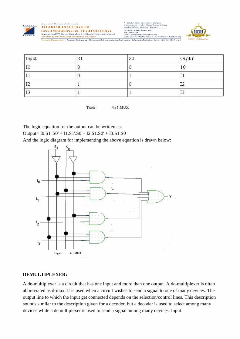
The logic equation for the output can be written as:
Output= I0.S1'.S0' + I1.S1'.S0 + I2.S1.S0' + I3.S1.S0
And the logic diagram for implementing the above equation is drawn below:
DEMULTIPLEXER:
A de-multiplexer is a circuit that has one input and more than one output. A de-multiplexer is often
abbreviated as d-mux. It is used when a circuit wishes to send a signal to one of many devices. The
output line to which the input get connected depends on the selection/control lines. This description
sounds similar to the description given for a decoder, but a decoder is used to select among many
devices while a demultiplexer is used to send a signal among many devices. Input
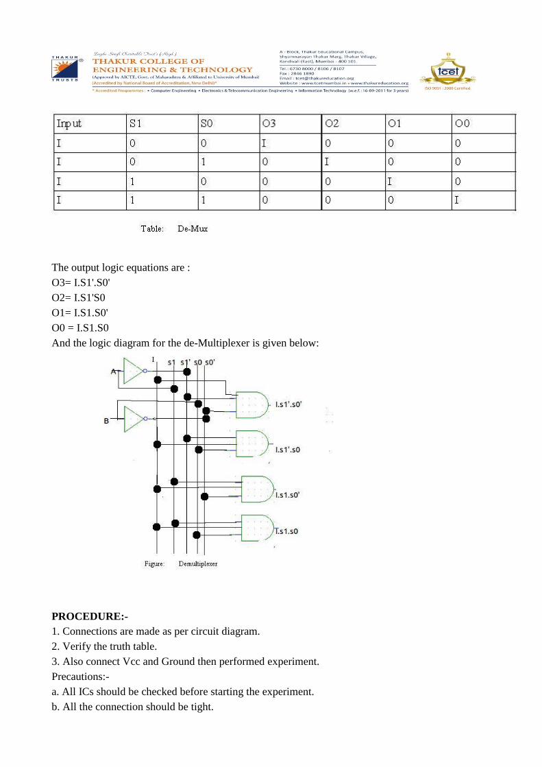
The output logic equations are :
O3= I.S1'.S0'
O2= I.S1'S0
O1= I.S1.S0'
O0 = I.S1.S0
And the logic diagram for the de-Multiplexer is given below:
PROCEDURE:-
1. Connections are made as per circuit diagram.
2. Verify the truth table.
3. Also connect Vcc and Ground then performed experiment.
Precautions:-
a. All ICs should be checked before starting the experiment.
b. All the connection should be tight.
c. Always connect ground first and then connect Vcc.
d. Suitable type wire should be used for different types of circuit.
e. The kit should be off before change the connections.
f. After completed the experiments switch off the supply of the apparatus
CONCLUSION: Thus verified 4 bit magnitude comparator.
LEARNING OUTCOMES:
LO1, LO2, LO3
COURSE OUTCOMES:
a) CO2
b) CO3
IMPORTANT QUESTIONS:
1. Why multiplexer is called as data selector?
2. Give the applications of multiplexer.
3. How many control inputs are there in 16 to 1 demultiplexer?
4. How many select lines will a 32:1 multiplexer will have?
5. What is a multiplexer?
6. How many select lines will a 16 to 1 multiplexer will have?
7. What is the function of enable input on a multiplexer chip?
8. What is a demultiplexer?
9. Differentiate between decoder and demultiplexer.
10. Why is a demultiplexer called data distributor?
11. Give the applications of decoder.
12. How many control inputs are there in 1:16 demultiplexer?
AIM: Implementation of Encoder and Decoder
LEARNING OBJECTIVES:
LOB1, LOB2, LOB3
TOOLS/SOFTWARE REQUIRED:
Logic gates (IC) trainer kit.
Connecting patch chords.
IC 7400, IC 7402, IC 7404, IC 7406, IC 7408, IC 7411, IC 7486
RELATED THEORY:
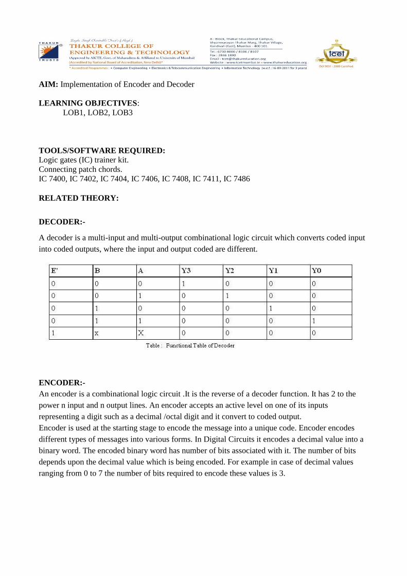
DECODER:-
A decoder is a multi-input and multi-output combinational logic circuit which converts coded input
into coded outputs, where the input and output coded are different.
ENCODER:-
An encoder is a combinational logic circuit .It is the reverse of a decoder function. It has 2 to the
power n input and n output lines. An encoder accepts an active level on one of its inputs
representing a digit such as a decimal /octal digit and it convert to coded output.
Encoder is used at the starting stage to encode the message into a unique code. Encoder encodes
different types of messages into various forms. In Digital Circuits it encodes a decimal value into a
binary word. The encoded binary word has number of bits associated with it. The number of bits
depends upon the decimal value which is being encoded. For example in case of decimal values
ranging from 0 to 7 the number of bits required to encode these values is 3.
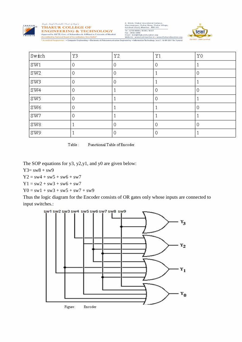
The SOP equations for y3, y2,y1, and y0 are given below:
Y3= sw8 + sw9
Y2 = sw4 + sw5 + sw6 + sw7
Y1 = sw2 + sw3 + sw6 + sw7
Y0 = sw1 + sw3 + sw5 + sw7 + sw9
Thus the logic diagram for the Encoder consists of OR gates only whose inputs are connected to
input switches.:
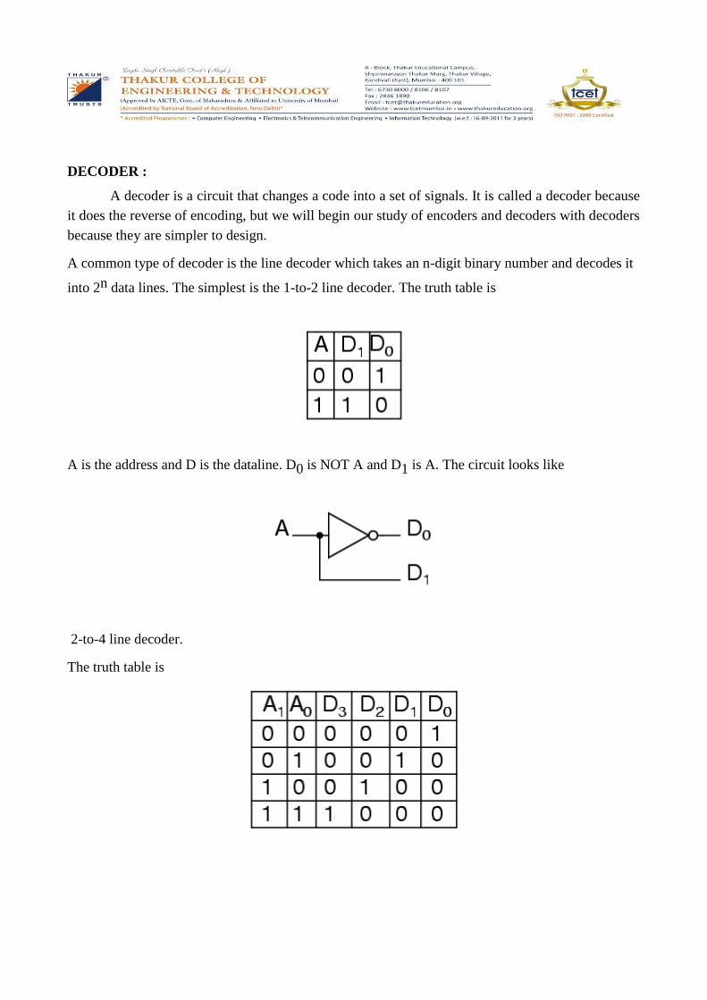
DECODER :
A decoder is a circuit that changes a code into a set of signals. It is called a decoder because
it does the reverse of encoding, but we will begin our study of encoders and decoders with decoders
because they are simpler to design.
A common type of decoder is the line decoder which takes an n-digit binary number and decodes it
into 2n data lines. The simplest is the 1-to-2 line decoder. The truth table is
A is the address and D is the dataline. D0 is NOT A and D1 is A. The circuit looks like
2-to-4 line decoder.
The truth table is
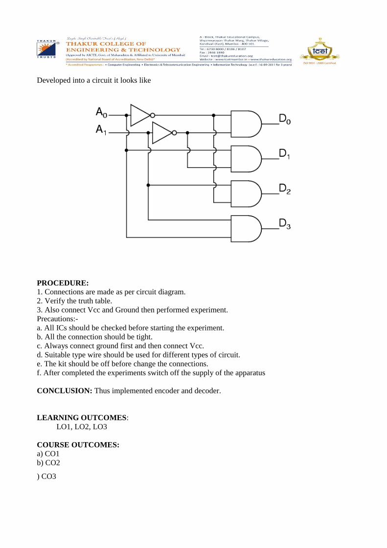
Developed into a circuit it looks like
PROCEDURE:
1. Connections are made as per circuit diagram.
2. Verify the truth table.
3. Also connect Vcc and Ground then performed experiment.
Precautions:-
a. All ICs should be checked before starting the experiment.
b. All the connection should be tight.
c. Always connect ground first and then connect Vcc.
d. Suitable type wire should be used for different types of circuit.
e. The kit should be off before change the connections.
f. After completed the experiments switch off the supply of the apparatus
CONCLUSION: Thus implemented encoder and decoder.
LEARNING OUTCOMES:
LO1, LO2, LO3
COURSE OUTCOMES: a) CO1
b) CO2
) CO3

IMPORTANT QUESTIONS
1. Differentiate between decoder and demultiplexer.
2. What is an encoder?
3. What is priority encoder?
4. Which digital system translates coded characters into a more useful form?
5. Why is a demultiplexer called data distributor?
6. Give the applications of decoder.
AIM: To verify and observe the operation of flip-flop (any two)
LEARNING OBJECTIVES: LOB4
TOOLS/SOFTWARE REQUIRED:
Logic gates (IC) trainer kit.
Connecting patch chords.
IC 7400, IC 7402, IC 7404, IC 7406, IC 7408, IC 7486
RELATED THEORY:
In case of sequential circuits the effect of all previous inputs on the outputs is represented by a state
of the circuit. Thus, the output of the circuit at any time depends upon its current state and the input.
These also determine the next state of the circuit . The relationship that exists among the inputs,
outputs, present and next states can be specified by either the state table or the state diagram. State
Table: - The state table representation of a sequential circuit consists of three sections labelled
present state next state and output. The present state designates the state of flip – flops before the
occurrence of a clock pulse. The next state shows the states of flip - flops after the clock pulse, and
the output section lists the value of the output variables during the present state.
Flip-Flop:-The basic one bit digital memory circuit is known as flip-flop. It can store either 0 or 1.
Flip-flops are classifieds according to the number of inputs.
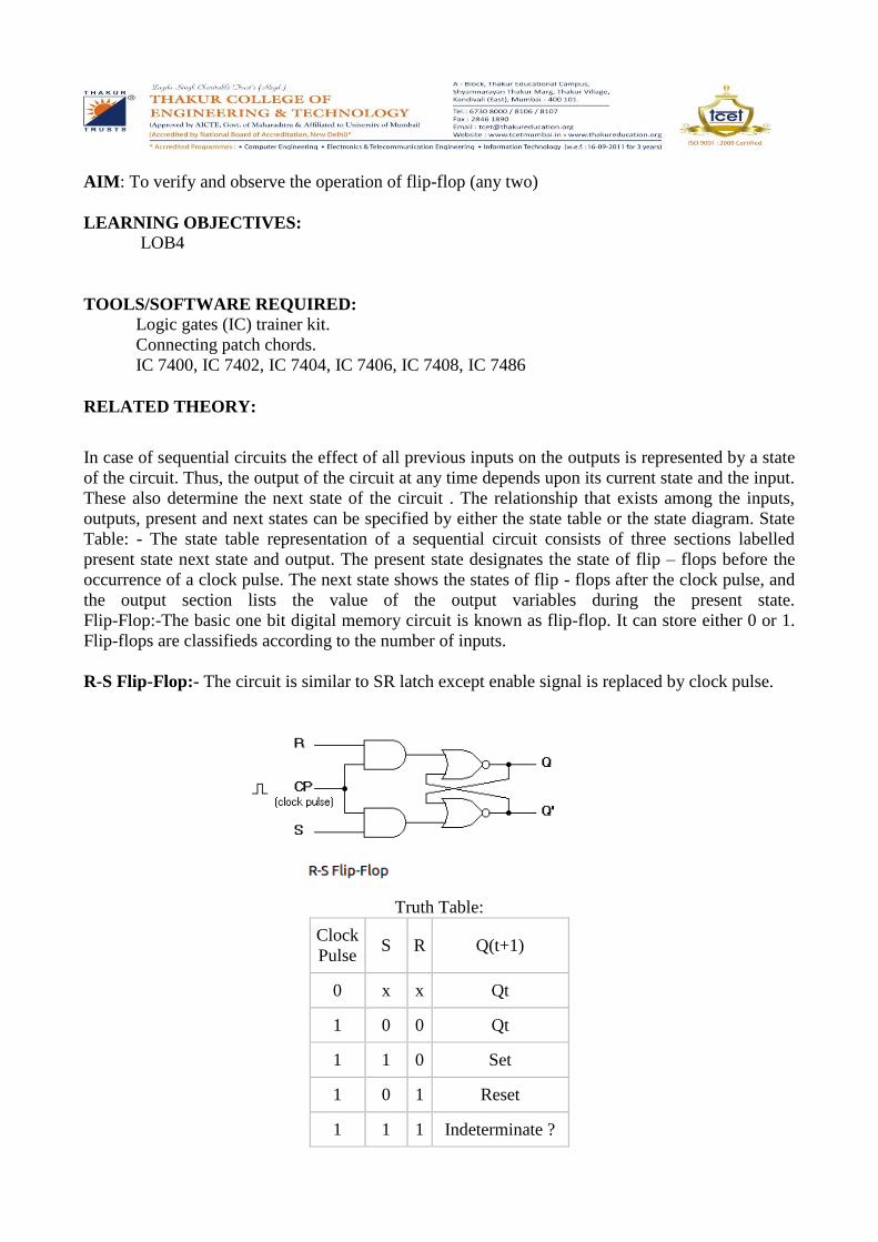
R-S Flip-Flop:- The circuit is similar to SR latch except enable signal is replaced by clock pulse.
Truth Table:
Clock
Pulse S R Q(t+1)
0 x x Qt
1 0 0 Qt
1 1 0 Set
1 0 1 Reset
1 1 1 Indeterminate ?
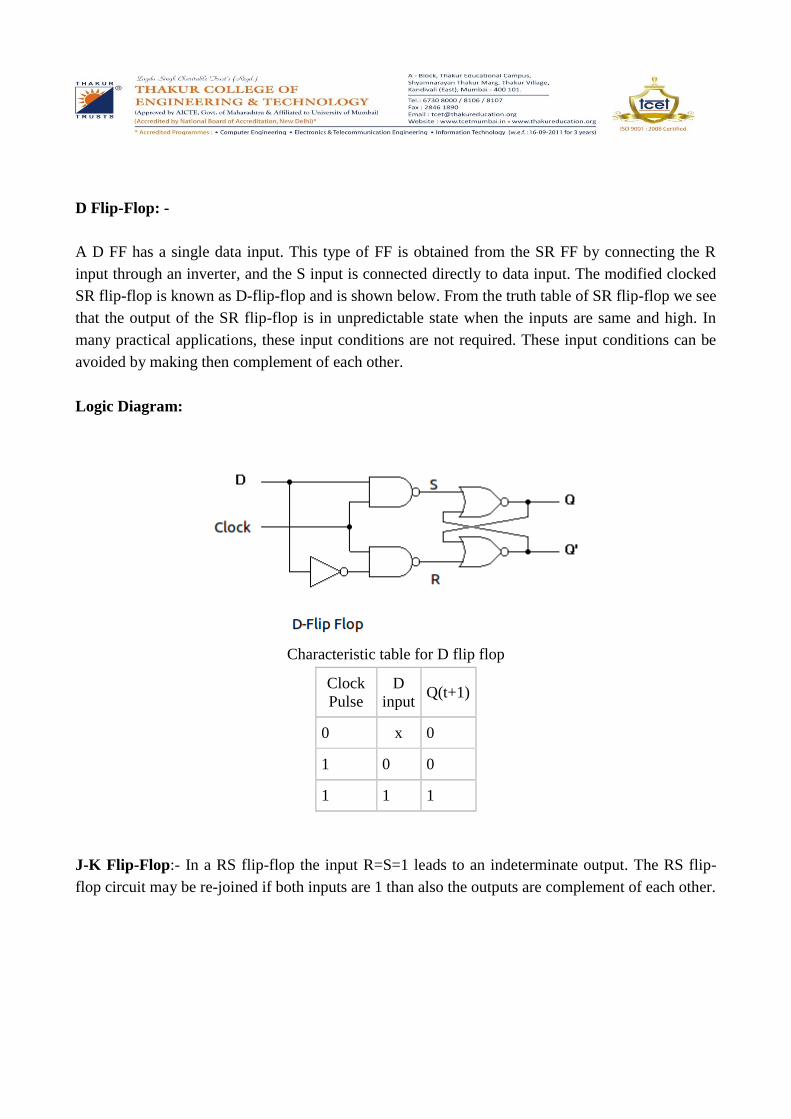
D Flip-Flop: -
A D FF has a single data input. This type of FF is obtained from the SR FF by connecting the R
input through an inverter, and the S input is connected directly to data input. The modified clocked
SR flip-flop is known as D-flip-flop and is shown below. From the truth table of SR flip-flop we see
that the output of the SR flip-flop is in unpredictable state when the inputs are same and high. In
many practical applications, these input conditions are not required. These input conditions can be
avoided by making then complement of each other.
Logic Diagram:
Characteristic table for D flip flop
Clock
Pulse
D
input Q(t+1)
0 x 0
1 0 0
1 1 1
J-K Flip-Flop:- In a RS flip-flop the input R=S=1 leads to an indeterminate output. The RS flip-
flop circuit may be re-joined if both inputs are 1 than also the outputs are complement of each other.
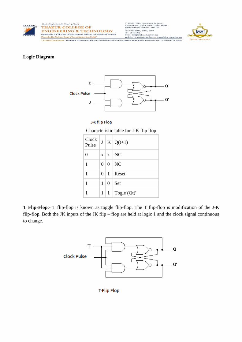
Logic Diagram
Characteristic table for J-K flip flop
Clock
Pulse J K Q(t+1)
0 x x NC
1 0 0 NC
1 0 1 Reset
1 1 0 Set
1 1 1 Togle (Qt)'
T Flip-Flop:- T flip-flop is known as toggle flip-flop. The T flip-flop is modification of the J-K
flip-flop. Both the JK inputs of the JK flip – flop are held at logic 1 and the clock signal continuous
to change.
Clock
Pulse
T
Input Q(t+1)
0 x NC
1 0 NC
1 1 Toggle
(Qt)'
PROCEDURE:-
1Connections are made as per circuit diagram.
2Verify truth- tables for various combinations of input.
CONCLUSION: Thus verified flip flop operation.
LEARNING OUTCOMES:
LO4
COURSE OUTCOMES:
a)CO2
b)CO3
c) CO5
IMPORTANT QUESTIONS:-
1) What is a latch?
2) What is a flip flop?
3) Differentiate between a latch and a flip flop.
4) What happens to the JK flip flop if the J input is treated as an inverter is wired between J and K
inputs?
5) How is a JK flip flop made to toggle?
6) When a JK flip flop is is in a no change condition?
7) Which is the basic sequential building block in which the output follows the data input as long as
the enable input is active?
8) Define the characteristic equation of a flip flop.
9) How many stable states a flip flop has?
AIM: To design any two shift register
LEARNING OBJECTIVES:
LOB4, LOB5
TOOLS/SOFTWARE REQUIRED:
Logic gates (IC) trainer kit.
Connecting patch chords.
IC 7474,IC 7404
RELATED THEORY:
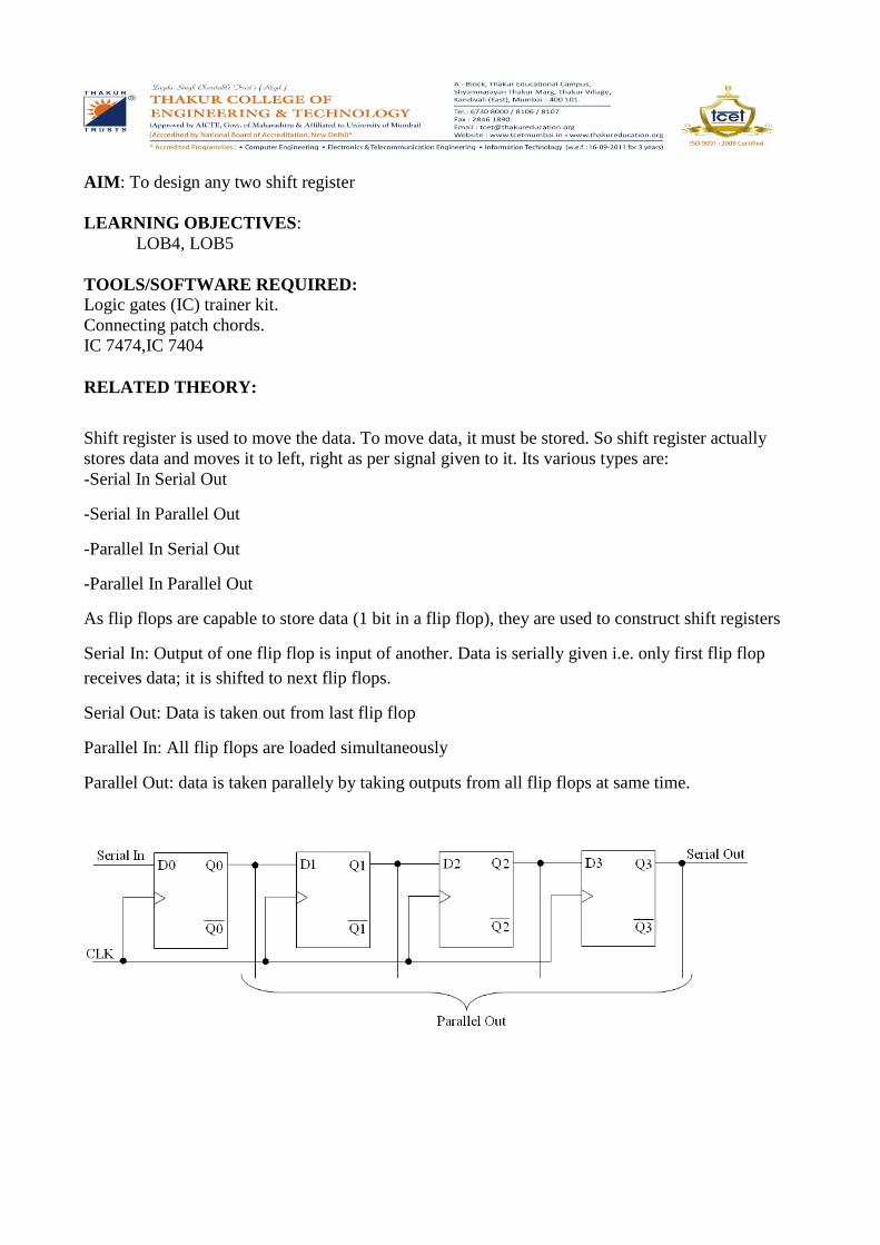
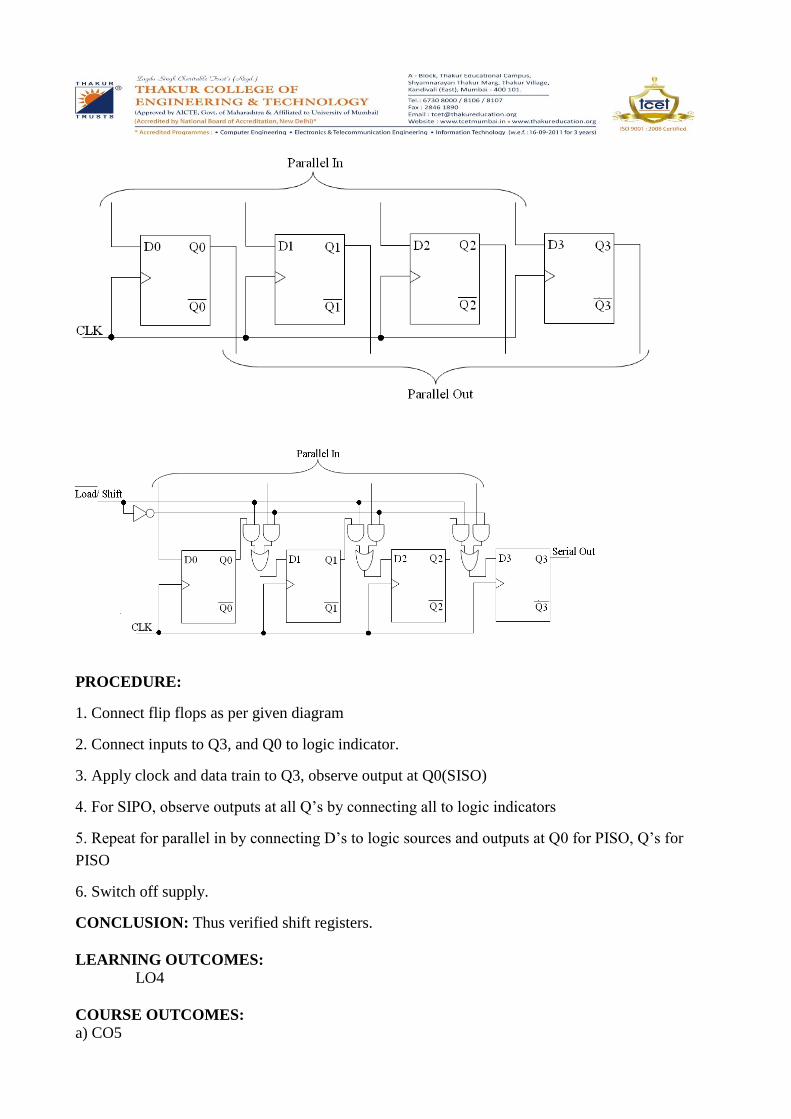
Shift register is used to move the data. To move data, it must be stored. So shift register actually
stores data and moves it to left, right as per signal given to it. Its various types are:
-Serial In Serial Out
-Serial In Parallel Out
-Parallel In Serial Out
-Parallel In Parallel Out
As flip flops are capable to store data (1 bit in a flip flop), they are used to construct shift registers
Serial In: Output of one flip flop is input of another. Data is serially given i.e. only first flip flop
receives data; it is shifted to next flip flops.
Serial Out: Data is taken out from last flip flop
Parallel In: All flip flops are loaded simultaneously
Parallel Out: data is taken parallely by taking outputs from all flip flops at same time.
PROCEDURE:
1. Connect flip flops as per given diagram
2. Connect inputs to Q3, and Q0 to logic indicator.
3. Apply clock and data train to Q3, observe output at Q0(SISO)
4. For SIPO, observe outputs at all Q’s by connecting all to logic indicators
5. Repeat for parallel in by connecting D’s to logic sources and outputs at Q0 for PISO, Q’s for
PISO
6. Switch off supply.
CONCLUSION: Thus verified shift registers.
LEARNING OUTCOMES:
LO4
COURSE OUTCOMES:
a) CO5
AIM: Implementation of Logic Gates using VHD
LEARNING OBJECTIVES:
LOB6
TOOLS/SOFTWARE REQUIRED:
VHDL installed on windows or Linux.
RELATED THEORY:
Explain
Entity
Architecture
Variables
Data types used in VHDL
For Logic gates refer related theory of experiment no 01 ….
Draw Flowchart and write algorithm.
CONCLUSION: Thus implemented logic gates using VHD
LEARNING OUTCOMES:
LO6
COURSE OUTCOMES:
a) CO6
Prepared by :
Ms. Swati Abhang