Course constraints beginning todayecee.colorado.edu/ecen4517/materials/Lecture9new.pdf · Switch to...
23
Power Electronics Lab 1 Course constraints beginning today Distance format, no on-campus lectures or lab sessions Campus isn’t closed (yet), but face-to-face contact is minimized Lectures to be held via Zoom on Mondays, 1:00-1:50 Slack channel activated Remainder of semester will cover Exp 4 via simulation and analytical design • Individual work and individual reports • Three parts, each comprising two weeks • We could have an Expo/competition at end of semester, if campus re-opens. Would be based on Exp. 3. Grading formula will be adjusted accordingly
Transcript of Course constraints beginning todayecee.colorado.edu/ecen4517/materials/Lecture9new.pdf · Switch to...

Power Electronics Lab 1
Course constraints beginning today
Distance format, no on-campus lectures or lab sessionsCampus isn’t closed (yet), but face-to-face contact is minimizedLectures to be held via Zoom on Mondays, 1:00-1:50Slack channel activatedRemainder of semester will cover Exp 4 via simulation and
analytical design• Individual work and individual reports• Three parts, each comprising two weeks• We could have an Expo/competition at end of semester, if campus
re-opens. Would be based on Exp. 3.Grading formula will be adjusted accordingly

Power Electronics Lab 2
Lecture 9ECEN 4517/5517
New Experiment 4Distance, remote format
Switch to LTspice
Part I—Open loop:Demonstrate open loop
simulation. Models of UC3525, gate drivers, nonlinear inductors, current-limited power supply
Part II—Closed loop with averaged model:
Demonstrate closed-loop system including op amp feedback circuitry. Plot loop gains etc.
Part III—Closed-Loop with switched model:Demonstrate working closed-loop system with switching model. Demonstrate start up transient response.
Power Electronics Lab 3
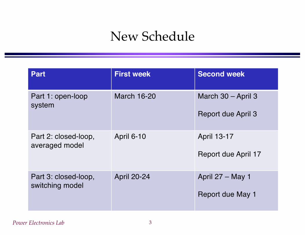
New Schedule
Part First week Second week
Part 1: open-loop system
March 16-20 March 30 – April 3
Report due April 3
Part 2: closed-loop, averaged model
April 6-10 April 13-17
Report due April 17
Part 3: closed-loop, switching model
April 20-24 April 27 – May 1
Report due May 1
Power Electronics Lab 4
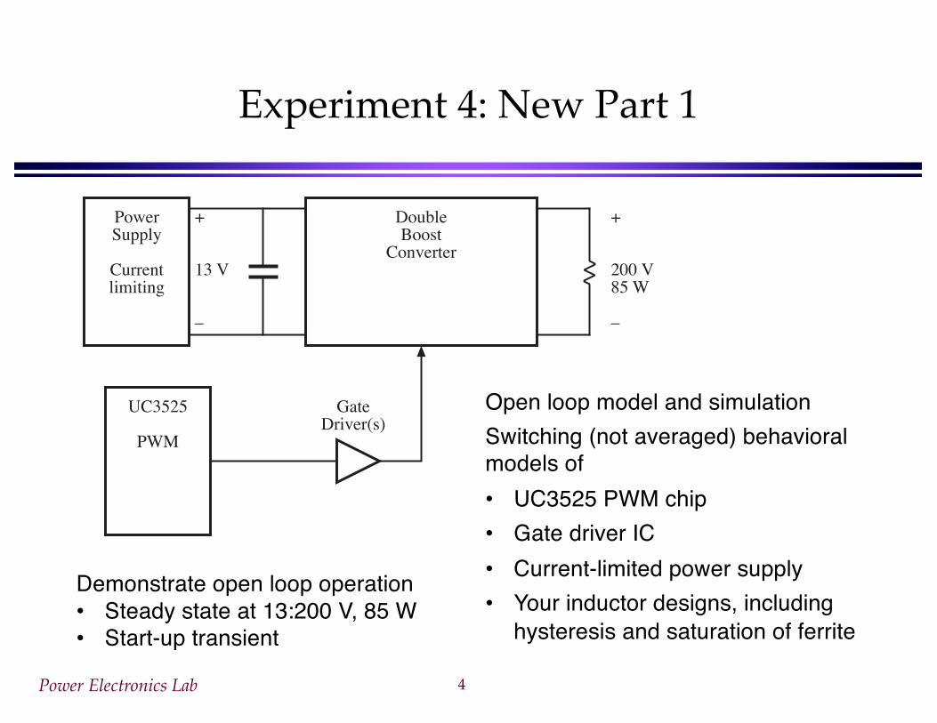
Experiment 4: New Part 1
PowerSupply
Currentlimiting
DoubleBoost
Converter
+
13 V
–
+
200 V85 W
–
UC3525
PWM
GateDriver(s)
Open loop model and simulationSwitching (not averaged) behavioral models of• UC3525 PWM chip• Gate driver IC• Current-limited power supply• Your inductor designs, including
hysteresis and saturation of ferrite
Demonstrate open loop operation• Steady state at 13:200 V, 85 W• Start-up transient

Power Electronics Lab 5
Lecture Topics
Get LTspice running on your personal computerModels for Part 1What is expected for Part 1

Introduction to Power Electronics 1-3: Simulation of Power Converters1
SPICE
Simulation Program with Integrated Circuit Emphasis• Enter a circuit, then run a simulation that
plots voltage or current waveforms, and computes other quantities of interest
In this course, we will use a version of SPICE that is available for free from the Linear Technology Corp., LTspice.
Versions of LTspice are available for both Windows and Macintosh systems, along with a getting started guide and examples.
Introduction to Power Electronics 1-3: Simulation of Power Converters2
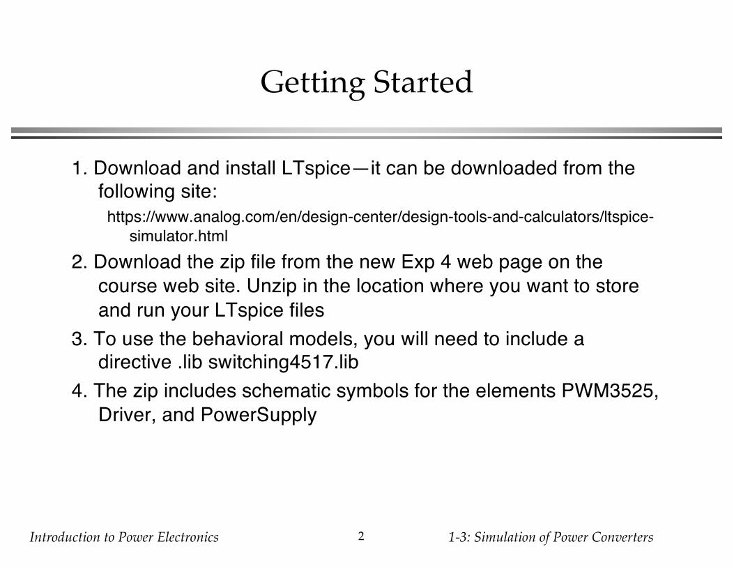
Getting Started
1. Download and install LTspice—it can be downloaded from the following site:
https://www.analog.com/en/design-center/design-tools-and-calculators/ltspice-simulator.html
2. Download the zip file from the new Exp 4 web page on the course web site. Unzip in the location where you want to store and run your LTspice files
3. To use the behavioral models, you will need to include adirective .lib switching4517.lib
4. The zip includes schematic symbols for the elements PWM3525, Driver, and PowerSupply

Introduction to Power Electronics 1-3: Simulation of Power Converters3
Parts Usage
Start with your Exp 4 Part 1 prelab design• You are welcome to change your design as appropriate• Use the ferrite cores in your parts kit• It is best to employ semiconductor models available in LTspice and
the behavioral models provided in the zip download• No ideal switches
MOSFET Voltage RonFDS5690 60 V 33 mΩIPI200N25N3 250 V 20 mΩ
Diode Voltage CurrentRF2001NS2D 200 V 10 ARFN5BM3S 350 V 5 A

Introduction to Power Electronics 1-3: Simulation of Power Converters4
Pulse-Width Modulator Block
The pulse-width modulator (PWM) converts an analog input voltage vc into a control switching waveform c whose duty cycle d is dependent on vc .Block functionality:D = (vc – Voffset)/VM (duty cycle of c(t))Frequency of c(t) is fs (switching frequency)Dmin ≤ d ≤ Dmax (duty cycle limits)In LTspice, the above parameters can be entered in a window obtained by right-clicking on the PWM block (or command-click on Macintosh)Defaults are: switching frequency of 100 kHz, Voffset = 1, VM = 2.3, Dmin = 0, Dmax = 0.95.
c(t)
vc(t)
Introduction to Power Electronics 1-3: Simulation of Power Converters5
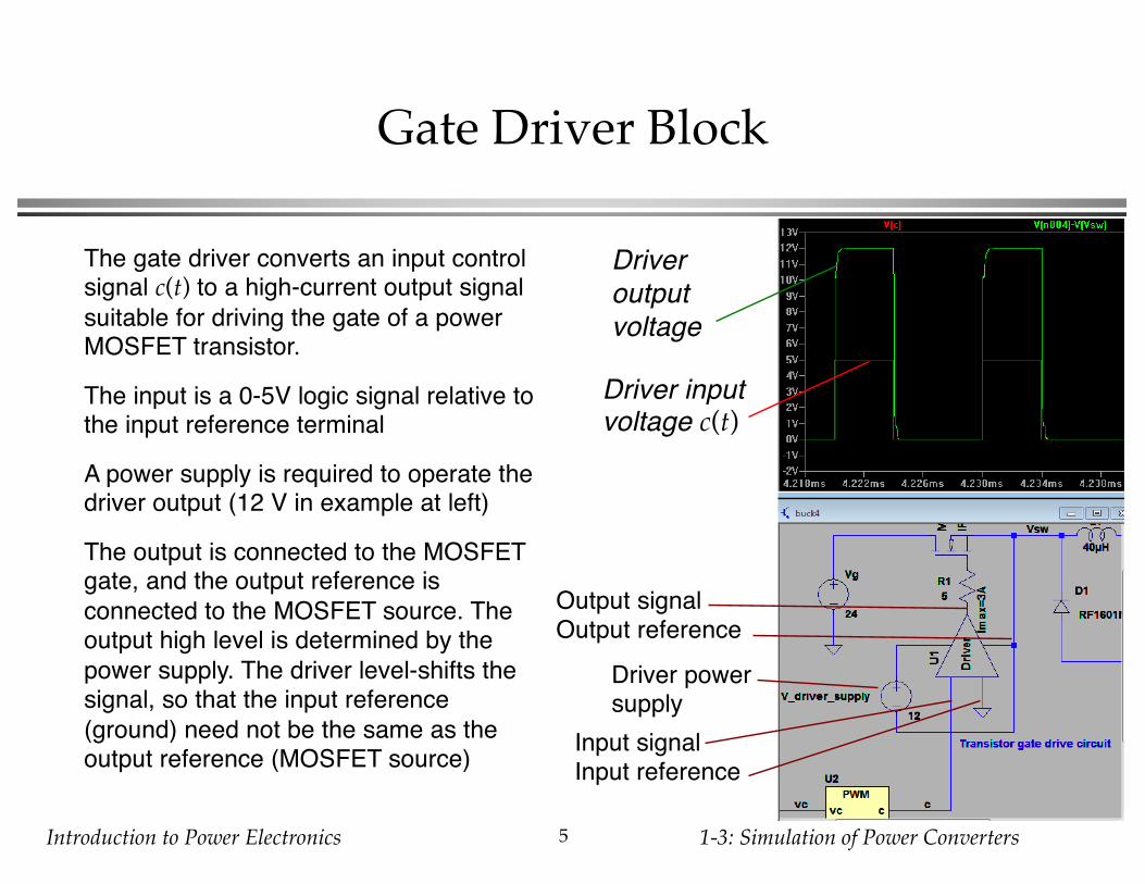
Gate Driver Block
Driver input voltage c(t)
Driver output voltage
The gate driver converts an input control signal c(t) to a high-current output signal suitable for driving the gate of a power MOSFET transistor.
The input is a 0-5V logic signal relative to the input reference terminal
A power supply is required to operate the driver output (12 V in example at left)
The output is connected to the MOSFET gate, and the output reference is connected to the MOSFET source. The output high level is determined by the power supply. The driver level-shifts the signal, so that the input reference (ground) need not be the same as the output reference (MOSFET source) Input signal
Input reference
Output signalOutput reference
Driver power supply

Introduction to Power Electronics 1-3: Simulation of Power Converters6
LTspice Simulation of Buck Converter
Example file included in zipMOSFET M1 and diode D1 operate as the switchThe converter input power source is Vg = 24 VThe converter output voltage Vout is applied to a load resistor Rload = 5 ohms.The simulation models several sources of loss:
Transistor and diode forward voltage dropsTransistor and diode switching lossesInductor winding resistance RLGate driver power consumption
Switch node voltage
Inductor current
Output voltage

Introduction to Power Electronics 1-3: Simulation of Power Converters7
Bench power supply with current limiting
Test your converter using a current-limited power supply, just like in the labVlim is the voltagesettingIlim is the current limit settingIn current limit mode,LTspice probably won’t converge when directly driving an inductor. Capacitor bypassing is needed.
Introduction to Power Electronics 1-3: Simulation of Power Converters8
Part 1
Implement your inductor designs using inductor modelincluding B-H hysteresis and saturation
Build LTspice model of open loop converter• Use current limited power supply• Use gate driver and PWM3525 models from zip file
Get your simulation to work, with 13 V input and outputof 200 V± 5 V at 85 W, in steady stateStart-up transient
• Use initial conditions of zero everywhere• Get your converter to start up without saturating your
inductors
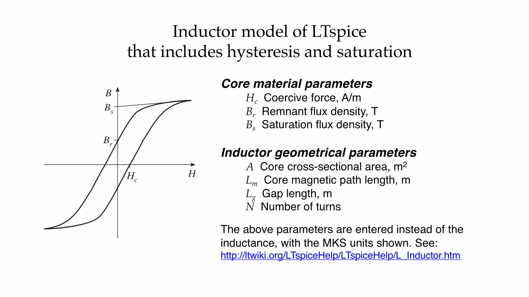
B
HHc
Br
Bs
Inductor model of LTspicethat includes hysteresis and saturation
Core material parametersHc Coercive force, A/mBr Remnant flux density, TBs Saturation flux density, T
Inductor geometrical parametersA Core cross-sectional area, m2
Lm Core magnetic path length, mLg Gap length, mN Number of turns
The above parameters are entered instead of the inductance, with the MKS units shown. See:http://ltwiki.org/LTspiceHelp/LTspiceHelp/L_Inductor.htm

Ferroxcube 3F3 Material (Ferrite)
Published B-H Characteristic
Hc = 12 A/m at 100˚C
Br = 120 mT= 0.12 Tat 100˚C
} Bs = 330-430 mT• Decreases as
temperature increases• We will use 0.33 T
B
HHc
Br
Bs
In this datasheet plot, the horizontal scale is 25 A/m per division, but division width becomes smaller above 50 A/m

Example40 µH inductor in a buck converter
• No saturation modeled• During steady state, the peak current is
between 2.5 A and 3 A• During turn-on transient, peak current
is over 7 A• Series resistance of 100 mΩ was
included in simulation modelLet’s design an inductor for this application, using the Kg design method
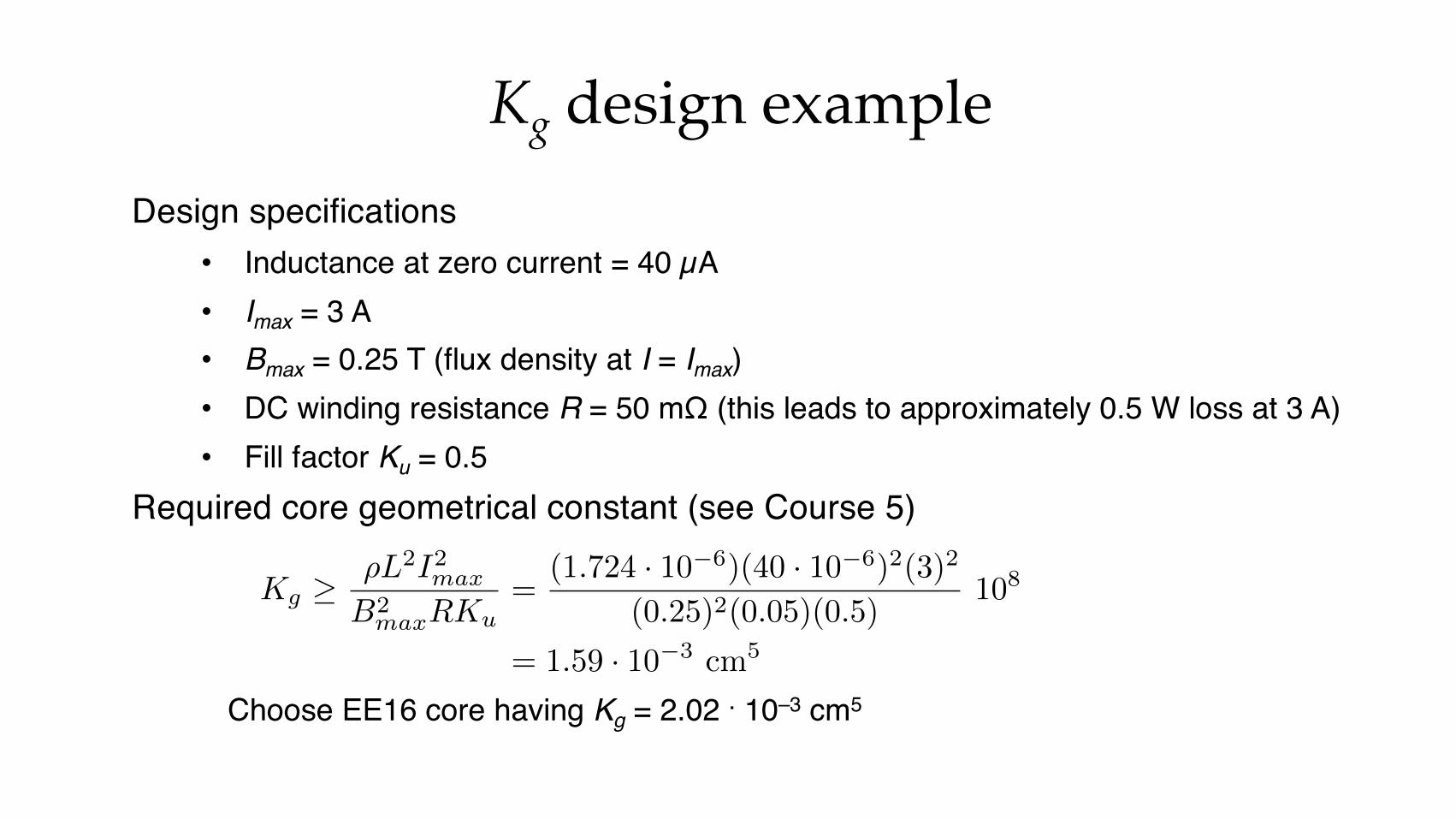
Kg design exampleDesign specifications
• Inductance at zero current = 40 µA• Imax = 3 A• Bmax = 0.25 T (flux density at I = Imax)• DC winding resistance R = 50 mΩ (this leads to approximately 0.5 W loss at 3 A)• Fill factor Ku = 0.5
Required core geometrical constant (see Course 5)
Choose EE16 core having Kg = 2.02 . 10–3 cm5
Kg � ⇢L2I2max
B2maxRKu
=(1.724 · 10�6)(40 · 10�6)2(3)2
(0.25)2(0.05)(0.5)108
= 1.59 · 10�3 cm5
1
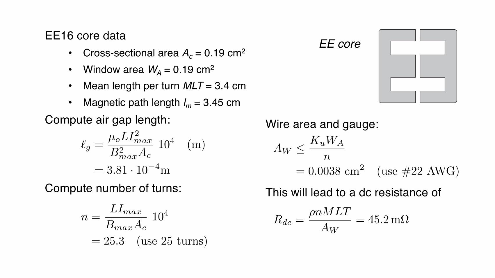
EE16 core data• Cross-sectional area Ac = 0.19 cm2
• Window area WA = 0.19 cm2
• Mean length per turn MLT = 3.4 cm• Magnetic path length lm = 3.45 cm
Compute air gap length:
AA
`g =µoLI2max
B2maxAc
104 (m)
= 3.81 · 10�4m
Compute number of turns:
n =LImax
BmaxAc104
= 25.3 (use 25 turns)
Wire area and gauge:
EE core
AW KuWA
n= 0.0038 cm2 (use #22 AWG)
This will lead to a dc resistance of
Rdc =⇢nMLT
AW= 45.2m⌦

Check flux density of this design, vs. winding current
With the approximation that the core reluctance is small, the flux density can be expressed as:
B =µonI
`g
I B
3 A 0.25 T
6 A 0.50 T
For the design values of the previous slide, this formula predicts the flux densities listed in the table above. • Indeed the flux density is 0.25 T at a winding current of 3 A, as intended. • At 6 A, the flux density will exceed the ferrite 3F3 material saturation flux
density of 0.33-0.43 T.
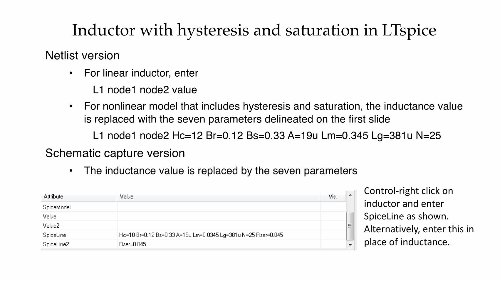
Inductor with hysteresis and saturation in LTspiceNetlist version
• For linear inductor, enterL1 node1 node2 value
• For nonlinear model that includes hysteresis and saturation, the inductance value is replaced with the seven parameters delineated on the first slide
L1 node1 node2 Hc=12 Br=0.12 Bs=0.33 A=19u Lm=0.345 Lg=381u N=25Schematic capture version
• The inductance value is replaced by the seven parameters
Control-right click on inductor and enter SpiceLine as shown. Alternatively, enter this in place of inductance.
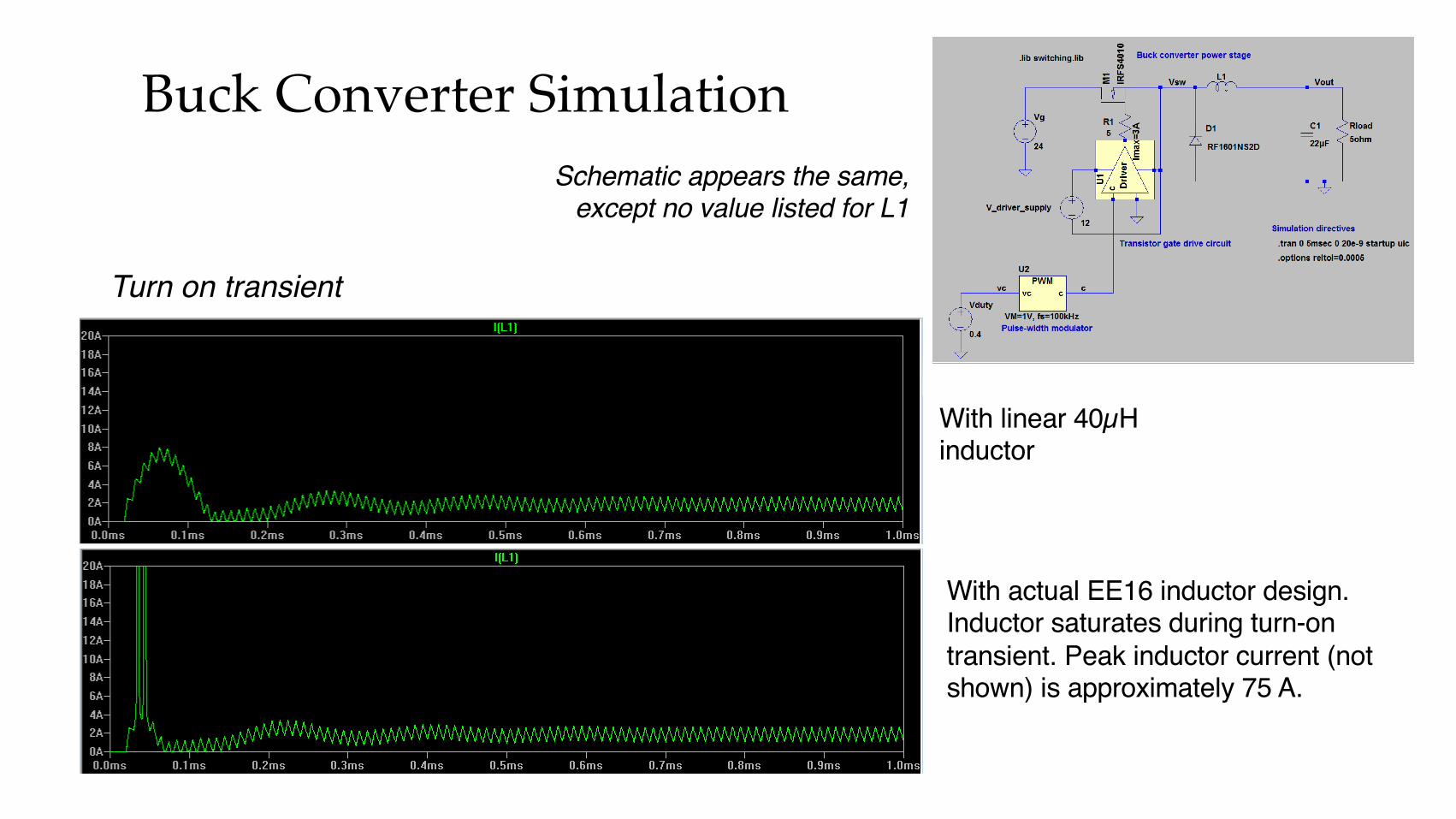
Buck Converter SimulationSchematic appears the same,
except no value listed for L1
Turn on transient
With linear 40µH inductor
With actual EE16 inductor design. Inductor saturates during turn-on transient. Peak inductor current (not shown) is approximately 75 A.

Inductor current approaching saturation
• Load resistance changed to 3 Ω• Magnified portion of turn on
transient
• Inductor current ripple appears linear at currents below 3.5 A
• At higher currents: slope increases as inductor saturates

Plotting B(t)
• LTspice labels axis in mA, but actual units are mT
• Saturation (substantial curvature) occurs for B(t) > 330 mT = 0.33 T
B(t) =µon
`gi(t) =
✓1
12
T
A
◆i(t)
1
• For this example, we can write
• So divide inductor current trace of previous slide by 12 to see B(t)