CoreSight Components Technical Reference Manual -...
376
Copyright © 2004-2009 ARM. All rights reserved. ARM DDI 0314H CoreSight ™ Components Technical Reference Manual
Transcript of CoreSight Components Technical Reference Manual -...
CoreSight™ Components
Technical Reference Manual
Copyright © 2004-2009 ARM. All rights reserved.ARM DDI 0314H
CoreSight ComponentsTechnical Reference Manual
Copyright © 2004-2009 ARM. All rights reserved.
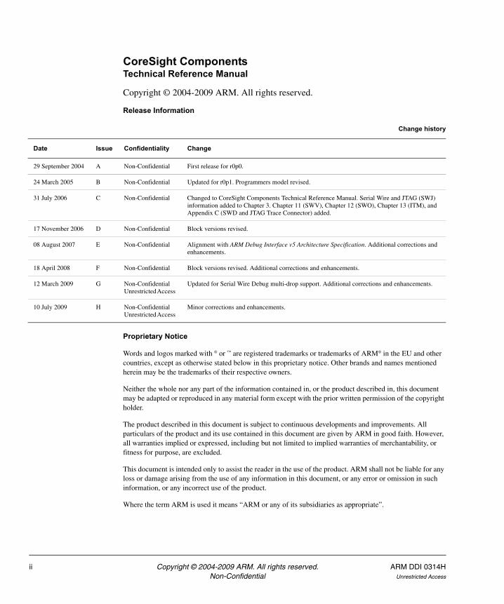
Release Information
Proprietary Notice
Words and logos marked with ® or ™ are registered trademarks or trademarks of ARM® in the EU and other countries, except as otherwise stated below in this proprietary notice. Other brands and names mentioned herein may be the trademarks of their respective owners.
Neither the whole nor any part of the information contained in, or the product described in, this document may be adapted or reproduced in any material form except with the prior written permission of the copyright holder.
The product described in this document is subject to continuous developments and improvements. All particulars of the product and its use contained in this document are given by ARM in good faith. However, all warranties implied or expressed, including but not limited to implied warranties of merchantability, or fitness for purpose, are excluded.
This document is intended only to assist the reader in the use of the product. ARM shall not be liable for any loss or damage arising from the use of any information in this document, or any error or omission in such information, or any incorrect use of the product.
Where the term ARM is used it means “ARM or any of its subsidiaries as appropriate”.
Change history
Date Issue Confidentiality Change
29 September 2004 A Non-Confidential First release for r0p0.
24 March 2005 B Non-Confidential Updated for r0p1. Programmers model revised.
31 July 2006 C Non-Confidential Changed to CoreSight Components Technical Reference Manual. Serial Wire and JTAG (SWJ) information added to Chapter 3. Chapter 11 (SWV), Chapter 12 (SWO), Chapter 13 (ITM), and Appendix C (SWD and JTAG Trace Connector) added.
17 November 2006 D Non-Confidential Block versions revised.
08 August 2007 E Non-Confidential Alignment with ARM Debug Interface v5 Architecture Specification. Additional corrections and enhancements.
18 April 2008 F Non-Confidential Block versions revised. Additional corrections and enhancements.
12 March 2009 G Non-Confidential Unrestricted Access
Updated for Serial Wire Debug multi-drop support. Additional corrections and enhancements.
10 July 2009 H Non-Confidential Unrestricted Access
Minor corrections and enhancements.
ii Copyright © 2004-2009 ARM. All rights reserved. ARM DDI 0314HNon-Confidential Unrestricted Access
Confidentiality Status
This document is Non-Confidential. The right to use, copy and disclose this document may be subject to license restrictions in accordance with the terms of the agreement entered into by ARM and the party that ARM delivered this document to.
Unrestricted Access is an ARM internal classification.
Product Status
The information in this document is final, that is for a developed product.
Web Address
http://www.arm.com
ARM DDI 0314H Copyright © 2004-2009 ARM. All rights reserved. iiiUnrestricted Access Non-Confidential

iv Copyright © 2004-2009 ARM. All rights reserved. ARM DDI 0314HNon-Confidential Unrestricted Access
ContentsCoreSight Components Technical Reference Manual
PrefaceAbout this book ............................................................................................. xxFeedback ................................................................................................... xxvi
Chapter 1 Introduction1.1 About the CoreSight components ............................................................... 1-21.2 CoreSight block summary ........................................................................... 1-41.3 Typical CoreSight Design Kit debugging environment ................................ 1-5
Chapter 2 Debug Access Port2.1 About the Debug Access Port ..................................................................... 2-22.2 SWJ-DP ...................................................................................................... 2-92.3 JTAG-DP ................................................................................................... 2-142.4 SW-DP ...................................................................................................... 2-162.5 Common debug port features and registers .............................................. 2-242.6 Access ports ............................................................................................. 2-382.7 AHB-AP ..................................................................................................... 2-392.8 APB-AP ..................................................................................................... 2-512.9 JTAG-AP ................................................................................................... 2-592.10 Auxiliary Access Port ................................................................................ 2-65
ARM DDI 0314H Copyright © 2004-2009 ARM. All rights reserved. vUnrestricted Access Non-Confidential
2.11 APB multiplexor ........................................................................................ 2-662.12 ROM table ................................................................................................ 2-722.13 Authentication requirements for Debug Access Port ................................ 2-742.14 Clocks, power, and resets ........................................................................ 2-75
Chapter 3 CoreSight Trace Sources3.1 AMBA AHB Trace Macrocell ...................................................................... 3-23.2 Embedded Trace Macrocells ...................................................................... 3-4
Chapter 4 Embedded Cross Trigger4.1 About the Embedded Cross Trigger ........................................................... 4-24.2 ECT programmers model ........................................................................... 4-84.3 Summary of CTI registers ........................................................................... 4-94.4 CTI register descriptions ........................................................................... 4-124.5 ECT Integration Test Registers ................................................................ 4-234.6 ECT CoreSight defined registers .............................................................. 4-284.7 ECT connectivity recommendations ......................................................... 4-304.8 ECT authentication requirements ............................................................ 4-35
Chapter 5 ATB 1:1 Bridge5.1 About the ATB 1:1 bridge ........................................................................... 5-25.2 Authentication requirements for ATB 1:1 Bridge ........................................ 5-4
Chapter 6 ATB Replicator6.1 About the ATB replicator ............................................................................ 6-26.2 ATB replicator connection behavior ............................................................ 6-36.3 Authentication requirements for replicators ................................................ 6-5
Chapter 7 CoreSight Trace Funnel7.1 About the CoreSight Trace Funnel ............................................................. 7-27.2 CSTF programmers model ......................................................................... 7-37.3 CSTF specific registers .............................................................................. 7-57.4 CSTF Integration Test Registers ................................................................ 7-97.5 CoreSight management registers for CSTF ............................................. 7-157.6 Unconnected slave interfaces .................................................................. 7-177.7 Disabled slave interfaces .......................................................................... 7-187.8 CSTF input arbitration .............................................................................. 7-197.9 Authentication requirements for funnels ................................................... 7-26
Chapter 8 Trace Port Interface Unit8.1 About the Trace Port Interface Unit ............................................................ 8-28.2 Trace Out Port ............................................................................................ 8-48.3 Miscellaneous connections ......................................................................... 8-58.4 TPIU programmers model .......................................................................... 8-68.5 TPIU CoreSight management registers ...................................................... 8-98.6 Trace port control registers ....................................................................... 8-11
vi Copyright © 2004-2009 ARM. All rights reserved. ARM DDI 0314HNon-Confidential Unrestricted Access
8.7 TPIU trace port sizes ................................................................................ 8-258.8 TPIU triggers ............................................................................................. 8-278.9 Other TPIU design considerations ............................................................ 8-298.10 Authentication requirements for TPIUs ..................................................... 8-338.11 TPIU pattern generator ............................................................................. 8-348.12 TPIU formatter and FIFO .......................................................................... 8-368.13 Configuration options ................................................................................ 8-388.14 Example configuration scenarios .............................................................. 8-39
Chapter 9 Embedded Trace Buffer9.1 About the ETB for CoreSight ...................................................................... 9-29.2 ETB programmers model ............................................................................ 9-59.3 ETB register descriptions ............................................................................ 9-89.4 ETB CoreSight management registers ..................................................... 9-229.5 ETB clocks, resets, and synchronization .................................................. 9-249.6 ETB Trace capture and formatting ............................................................ 9-259.7 Flush assertion .......................................................................................... 9-309.8 Triggers ..................................................................................................... 9-349.9 Write address generation for trace data storage ....................................... 9-369.10 Trace data storage .................................................................................... 9-379.11 APB configuration and RAM access ......................................................... 9-389.12 Trace RAM ................................................................................................ 9-399.13 Authentication requirements for CoreSight ETBs ..................................... 9-409.14 ETB RAM support ..................................................................................... 9-419.15 ETB configuration options ......................................................................... 9-429.16 Comparisons with ETB11 .......................................................................... 9-43
Chapter 10 Serial Wire Viewer10.1 About the Serial Wire Viewer .................................................................... 10-210.2 SWV interfaces ......................................................................................... 10-310.3 Authentication requirements ..................................................................... 10-5
Chapter 11 Serial Wire Output11.1 About the Serial Wire Output .................................................................... 11-211.2 SWO ports ................................................................................................ 11-311.3 SWO programmers model ........................................................................ 11-411.4 CoreSight defined registers ...................................................................... 11-611.5 Trace port control registers ....................................................................... 11-911.6 Trigger registers ...................................................................................... 11-1111.7 EXTCTL registers ................................................................................... 11-1211.8 Test pattern registers .............................................................................. 11-1311.9 Formatter and flush registers .................................................................. 11-1411.10 Integration test registers ......................................................................... 11-1611.11 SWO trace port ....................................................................................... 11-18
ARM DDI 0314H Copyright © 2004-2009 ARM. All rights reserved. viiUnrestricted Access Non-Confidential
Chapter 12 Instrumentation Trace Macrocell12.1 About the Instrumentation Trace Macrocell .............................................. 12-212.2 ITM ports .................................................................................................. 12-912.3 ITM programmers model ........................................................................ 12-1012.4 CoreSight defined registers .................................................................... 12-1212.5 Stimulus registers ................................................................................... 12-1412.6 Trace registers ........................................................................................ 12-1612.7 Control registers ..................................................................................... 12-1812.8 Integration test registers ......................................................................... 12-2112.9 Authentication requirements ................................................................... 12-25
Appendix A CoreSight Port ListA.1 Clock domains ............................................................................................ A-2A.2 CoreSight DAP signals ............................................................................... A-3A.3 CoreSight ECT signals ............................................................................... A-9A.4 CoreSight replicator signals ...................................................................... A-12A.5 CoreSight synchronous bridge signals ..................................................... A-14A.6 CoreSight trace funnel signals .................................................................. A-15A.7 CoreSight TPIU signals ............................................................................ A-19A.8 CoreSight ETB signals ............................................................................. A-21A.9 CoreSight SWO signals ............................................................................ A-23A.10 CoreSight ITM signals .............................................................................. A-24
Appendix B CoreSight Components and Clock DomainsB.1 CoreSight components and clock domains ................................................ B-2
Appendix C Serial Wire Debug and JTAG Trace ConnectorC.1 About the SWD and JTAG trace connector ................................................ C-2C.2 Pinout details .............................................................................................. C-3C.3 Signal definitions ........................................................................................ C-8
Appendix D Deprecated SWJ-DP Switching SequencesD.1 About the deprecated SWJ-DP switching sequences ................................ D-2
Appendix E Revisions
Glossary
viii Copyright © 2004-2009 ARM. All rights reserved. ARM DDI 0314HNon-Confidential Unrestricted Access
List of TablesCoreSight Components Technical Reference Manual
Change history .............................................................................................................. iiTable 1-1 CoreSight block summary ......................................................................................... 1-4Table 2-1 JTAG-DP physical interface .................................................................................... 2-15Table 2-2 JTAG-DP registers .................................................................................................. 2-15Table 2-3 Terms used in SW-DP timing .................................................................................. 2-19Table 2-4 TARGETID input connections ................................................................................. 2-22Table 2-5 TARGETID mapping ............................................................................................... 2-22Table 2-6 Summary of Debug Port registers ........................................................................... 2-26Table 2-7 AP Abort Register bit assignments ......................................................................... 2-27Table 2-8 Identification Code Register bit assignments .......................................................... 2-28Table 2-9 JEDEC JEP-106 manufacturer ID code, with ARM values ..................................... 2-29Table 2-10 Control/Status Register bit assignments ................................................................. 2-30Table 2-11 AP Select Register bit assignments ........................................................................ 2-32Table 2-12 Wire Control Register bit assignments .................................................................... 2-34Table 2-13 Turnaround tristate period field bit definitions ......................................................... 2-35Table 2-14 Wire operating mode bit definitions ......................................................................... 2-35Table 2-15 Target Identification Register bit assignments ........................................................ 2-36Table 2-16 Data Link Protocol Identification Register bit assignments ..................................... 2-37Table 2-17 Other AHB-AP ports ................................................................................................ 2-40Table 2-18 Example generation of byte lane strobes ................................................................ 2-41Table 2-19 AHB access port registers ....................................................................................... 2-43
ARM DDI 0314H Copyright © 2004-2009 ARM. All rights reserved. ixUnrestricted Access Non-Confidential
Table 2-20 AHB-AP Control/Status Word Register bit assignments ......................................... 2-44Table 2-21 AHB-AP Transfer Address Register bit assignments ............................................. 2-46Table 2-22 AHB-AP Data Read/Write Register bit assignments .............................................. 2-46Table 2-23 Banked Data Register bit assignments ................................................................... 2-46Table 2-24 ROM Address Register bit assignments ................................................................. 2-47Table 2-25 AHB-AP Identification Register bit assignments ..................................................... 2-47Table 2-26 Error responses with DAPSLVERR HIGH and TrInProg LOW ............................... 2-49Table 2-27 APB-AP other ports ................................................................................................ 2-51Table 2-28 APB-AP registers .................................................................................................... 2-52Table 2-29 APB Control/Status Word Register bit assignments ............................................... 2-53Table 2-30 APB-AP Transfer Address Register bit assignments .............................................. 2-55Table 2-31 ABP-AP Data Read/Write Register bit assignments ............................................... 2-55Table 2-32 APB-AP Banked Data Registers bit assignments ................................................... 2-56Table 2-33 Debug APB ROM Address Register bit assignments ............................................. 2-56Table 2-34 APB-AP Identification Register bit assignments ..................................................... 2-57Table 2-35 JTAG to slave device signals .................................................................................. 2-59Table 2-36 JTAG-AP register summary .................................................................................... 2-61Table 2-37 JTAG-AP Control/Status Word Register bit assignments ....................................... 2-62Table 2-38 JTAG-AP Port Select Register bit assignments ...................................................... 2-63Table 2-39 JTAG-AP Port Status Register bit assignments ..................................................... 2-63Table 2-40 JTAG-AP Identification Register bit assignments ................................................... 2-64Table 2-41 APB-Mux miscellaneous signals ............................................................................. 2-68Table 2-42 ROM table registers ................................................................................................ 2-72Table 2-43 ROM table entries bit assignments ......................................................................... 2-73Table 4-1 CTI register summary ............................................................................................... 4-9Table 4-2 CTI Control Register bit assignments ..................................................................... 4-12Table 4-3 CTI Interrupt Acknowledge Register bit assignments ............................................. 4-13Table 4-4 CTI Application Trigger Set Register bit assignments ............................................ 4-14Table 4-5 CTI Application Trigger Clear Register bit assignments ......................................... 4-15Table 4-6 CTI Application Pulse Register bit assignments ..................................................... 4-15Table 4-7 CTI Trigger to Channel Enable Registers bit assignments ..................................... 4-16Table 4-8 CTI Channel to Trigger Enable Registers bit assignments ..................................... 4-17Table 4-9 CTI Trigger In Status Register bit assignments ...................................................... 4-18Table 4-10 CTI Trigger Out Status Register bit assignments ................................................... 4-18Table 4-11 CTI Channel In Status Register bit assignments .................................................... 4-19Table 4-12 CTI Channel Out Status Register bit assignments ................................................. 4-20Table 4-13 CTI Channel Gate Register bit assignments .......................................................... 4-20Table 4-14 External Multiplexor Control Register bit assignments ........................................... 4-22Table 4-15 ITCHINACK Register bit assignments .................................................................... 4-23Table 4-16 ITTRIGINACK Register bit assignments ................................................................. 4-24Table 4-17 ITCHOUT Register bit assignments ....................................................................... 4-24Table 4-18 ITTRIGOUT Register bit assignments .................................................................... 4-25Table 4-19 ITCHOUTACK Register bit assignments ................................................................ 4-25Table 4-20 ITTRIGOUTACK Register bit assignments ............................................................. 4-26Table 4-21 ITCHIN Register bit assignments ........................................................................... 4-26Table 4-22 ITTRIGIN Register bit assignments ........................................................................ 4-27Table 4-23 Authentication values for ECT ................................................................................ 4-28
x Copyright © 2004-2009 ARM. All rights reserved. ARM DDI 0314HNon-Confidential Unrestricted Access
Table 4-24 Device ID bit values ................................................................................................ 4-29Table 4-25 Trigger input connections for ARM7 and ARM9 systems ........................................ 4-30Table 4-26 Trigger output connections for ARM7 and ARM9 systems ..................................... 4-31Table 4-27 Recommended input connections for use with ARM11 systems ............................ 4-32Table 4-28 Recommended output connections for use with ARM11 systems .......................... 4-32Table 4-29 Trigger inputs to the CTI ......................................................................................... 4-33Table 4-30 Trigger outputs from CTI ......................................................................................... 4-34Table 4-31 ECT recommended trigger outputs ......................................................................... 4-35Table 4-32 ECT authentication signals ..................................................................................... 4-36Table 7-1 CSTF visible registers ............................................................................................... 7-3Table 7-2 CSTF Control Register bit assignments .................................................................... 7-6Table 7-3 CSTF Priority Control Register bit assignments ........................................................ 7-7Table 7-4 Integration Test ATB Data 0 Register bit assignments on reads ............................ 7-10Table 7-5 Integration Test ATB Data 0 Register bit assignments on writes ............................ 7-10Table 7-6 Integration Test ATB Control 2 Register bit assignments on reads ........................ 7-11Table 7-7 Integration Test ATB Control 2 Register bit assignments on writes ........................ 7-11Table 7-8 Integration Test ATB Control 1 Register bit assignments on reads ........................ 7-12Table 7-9 Integration Test ATB Control 1 Register bit assignments on writes ........................ 7-12Table 7-10 Integration Test ATB Control 1 Register bit assignments on reads ........................ 7-13Table 7-11 Integration Test ATB Control 0 Register bit assignments on writes ........................ 7-14Table 7-12 CSTF Device ID bit assignments ............................................................................ 7-15Table 7-13 Tie-offs for unconnected ports ................................................................................ 7-17Table 8-1 Trace Out Port signals .............................................................................................. 8-4Table 8-2 TPIU miscellaneous ports ......................................................................................... 8-5Table 8-3 TPIU programmable registers ................................................................................... 8-6Table 8-4 Device ID bit values .................................................................................................. 8-9Table 8-5 Supported Trigger Modes Register bit assignments ............................................... 8-12Table 8-6 Trigger Counter Register bit assignments ............................................................... 8-13Table 8-7 Supported Trigger Multiplier Register bit assignments ............................................ 8-14Table 8-8 Supported Test Patterns/Modes Register bit assignments ..................................... 8-15Table 8-9 Test Pattern Repeat Counter Register bit assignments .......................................... 8-16Table 8-10 Formatter and Flush Status Register bit assignments ............................................ 8-17Table 8-11 Formatter and Flush Control Register bit assignments ........................................... 8-18Table 8-12 Formatter Synchronization Counter Register bit assignments ................................ 8-20Table 8-13 Integration Test Trigger In and Flush In Acknowledge Register bit assignments ... 8-21Table 8-14 Integration Test Trigger In and Flush In Register bit assignments .......................... 8-22Table 8-15 Integration Test ATB Data Register 0 bit assignments ........................................... 8-22Table 8-16 Integration Test ATB Control Register 2 bit assignments ....................................... 8-23Table 8-17 Integration Test ATB Control Register 1 bit assignments ....................................... 8-23Table 8-18 Integration Test ATB Control Register 0 bit assignments ....................................... 8-24Table 8-19 Example Trace Out Port sizes ................................................................................ 8-25Table 8-20 CoreSight representation of triggers ....................................................................... 8-27Table 9-1 ETB triggering and flushing ports .............................................................................. 9-3Table 9-2 ETB status ports ........................................................................................................ 9-4Table 9-3 ETB Memory BIST interface ports ............................................................................ 9-4Table 9-4 ETB register summary .............................................................................................. 9-5Table 9-5 ETB RAM Depth Register bit assignments ............................................................... 9-8
ARM DDI 0314H Copyright © 2004-2009 ARM. All rights reserved. xiUnrestricted Access Non-Confidential

Table 9-6 ETB Status Register bit assignments. ...................................................................... 9-9Table 9-7 ETB RAM Read Data Register bit assignments. ...................................................... 9-9Table 9-8 ETB RAM Read Pointer Register bit assignments. ................................................ 9-10Table 9-9 ETB RAM Write Pointer Register bit assignments. ................................................. 9-10Table 9-10 ETB Trigger Counter Register bit assignments. ..................................................... 9-11Table 9-11 ETB Control Register bit assignments. ................................................................... 9-12Table 9-12 ETB RAM Write Data Register bit assignments ..................................................... 9-12Table 9-13 ETB Formatter and Flush Status Register bit assignments .................................... 9-13Table 9-14 ETB Formatter and Flush Control Register bit assignments .................................. 9-14Table 9-15 Integration Test Miscellaneous Output Register 0 bit assignments ........................ 9-17Table 9-16 Integration Test Trigger In and Flush In Acknowledge Register bit assignments ... 9-17Table 9-17 ETB for CoreSight Integration Register, ITTRFLIN bit assignments ...................... 9-18Table 9-18 Integration Test ATB Data Register 0 bit assignments ........................................... 9-19Table 9-19 Integration Test ATB Control Register 2 bit assignments ....................................... 9-19Table 9-20 Integration Test ATB Control Register 1 bit assignments ....................................... 9-20Table 9-21 Integration Test ATB Control Register 0 bit assignments ....................................... 9-21Table 9-22 CSTF Device ID bit assignments ............................................................................ 9-22Table 9-23 ETB RAM size options ............................................................................................ 9-42Table 9-24 ETB11 and ETB comparison .................................................................................. 9-43Table 10-1 Trace interface ports ............................................................................................... 10-3Table 10-2 Miscellaneous ports ................................................................................................ 10-4Table 10-3 Authentication interface ports ................................................................................. 10-5Table 11-1 Trace out ports ........................................................................................................ 11-3Table 11-2 SWO programmable registers ................................................................................ 11-4Table 11-3 Lock Status Register bit assignments ..................................................................... 11-7Table 11-4 Device ID Register bit assignments ........................................................................ 11-7Table 11-5 Current Output Divisor Register bit assignments .................................................. 11-10Table 11-6 Selected Pin Protocol Register bit assignments ................................................... 11-10Table 11-7 Formatter and Flush Status Register bit assignments .......................................... 11-14Table 11-8 Integration Test ATB Data Register 0 bit assignments ......................................... 11-16Table 11-9 Integration Test ATB Control Register 2 bit assignments ..................................... 11-17Table 11-10 Integration Test ATB Control Register 0 bit assignments ..................................... 11-17Table 11-11 Manchester pin protocol encoding ........................................................................ 11-19Table 11-12 UART pin protocol encoding ................................................................................. 11-20Table 12-1 Sync packet encoding ............................................................................................. 12-3Table 12-2 Trace packet encoding ........................................................................................... 12-3Table 12-3 ITM packet priority levels ........................................................................................ 12-8Table 12-4 Miscellaneous ports ................................................................................................ 12-9Table 12-5 ITM programmable registers ................................................................................. 12-10Table 12-6 Trace Enable Register bit assignments ................................................................ 12-16Table 12-7 Trace Trigger Register bit assignments ................................................................ 12-16Table 12-8 Control Register bit assignments .......................................................................... 12-18Table 12-9 Synchronization Control Register bit assignments ............................................... 12-20Table 12-10 Integration Test Trigger Out Acknowledge Register bit assignments ................... 12-21Table 12-11 Integration Test Trigger Out Register bit assignments ......................................... 12-22Table 12-12 Integration Test ATB Data Register 0 bit assignments ......................................... 12-22Table 12-13 Integration Test ATB Control Register 2 bit assignments ..................................... 12-23
xii Copyright © 2004-2009 ARM. All rights reserved. ARM DDI 0314HNon-Confidential Unrestricted Access
Table 12-14 Integration Test ATB Control Register 1 bit assignments ..................................... 12-23Table 12-15 Integration Test ATB Control Register 0 bit assignments ..................................... 12-24Table 12-16 Authentication interface ports ................................................................................ 12-25Table A-1 CoreSight DAP signals .............................................................................................. A-3Table A-2 CoreSight CTI signals ............................................................................................... A-9Table A-3 CoreSight CTM signals ........................................................................................... A-10Table A-4 CoreSight replicator signals .................................................................................... A-12Table A-5 CoreSight synchronous bridge signals .................................................................... A-14Table A-6 CoreSight trace funnel signals ................................................................................ A-15Table A-7 CoreSight TPIU signals ........................................................................................... A-19Table A-8 CoreSight ETB signals ............................................................................................ A-21Table A-9 CoreSight SWO signals .......................................................................................... A-23Table A-10 CoreSight ITM signals ............................................................................................. A-24Table B-1 CoreSight components and clock domains ............................................................... B-2Table C-1 Summary of pin names ............................................................................................ C-3Table C-2 10-way connector for SWD or JTAG systems .......................................................... C-5Table C-3 20-way connector for future SWD or JTAG systems ................................................ C-6Table C-4 Generic signal definitions ......................................................................................... C-8Table D-1 Deprecated switching sequences ............................................................................ D-2Table E-1 Differences between issue E and issue F ................................................................. E-1Table E-2 Differences between issue F and issue G ................................................................. E-2Table E-3 Differences between issue G and issue H ................................................................ E-3
ARM DDI 0314H Copyright © 2004-2009 ARM. All rights reserved. xiiiUnrestricted Access Non-Confidential

xiv Copyright © 2004-2009 ARM. All rights reserved. ARM DDI 0314HNon-Confidential Unrestricted Access
List of FiguresCoreSight Components Technical Reference Manual
Key to timing diagram conventions .......................................................................... xxiiiFigure 1-1 CoreSight debugging environment ............................................................................ 1-5Figure 2-1 Structure of the CoreSight DAP components ............................................................ 2-3Figure 2-2 SWJ Debug Port ....................................................................................................... 2-4Figure 2-3 AHB Access Port ....................................................................................................... 2-4Figure 2-4 APB Access Port ....................................................................................................... 2-5Figure 2-5 DAP flow of control .................................................................................................... 2-7Figure 2-6 SWJ-DP external connections ................................................................................ 2-10Figure 2-7 SWJ-DP signal clamping ......................................................................................... 2-12Figure 2-8 SW-DP acknowledgement timing ............................................................................ 2-19Figure 2-9 SW-DP to DAP bus timing for write ......................................................................... 2-20Figure 2-10 SW-DP to DAP bus timing for read ......................................................................... 2-20Figure 2-11 SW-DP idle timing ................................................................................................... 2-21Figure 2-12 AP Abort Register bit assignments ......................................................................... 2-27Figure 2-13 Identification Code Register bit assignments .......................................................... 2-28Figure 2-14 Control/Status Register bit assignments ................................................................. 2-29Figure 2-15 AP Select Register bit assignments ........................................................................ 2-32Figure 2-16 Wire Control Register bit assignments .................................................................... 2-34Figure 2-17 Target Identification Register bit assignments ........................................................ 2-36Figure 2-18 Data Link Protocol Identification Register bit assignments ..................................... 2-37Figure 2-19 AHB-AP Control/Status Word Register bit assignments ......................................... 2-44
ARM DDI 0314H Copyright © 2004-2009 ARM. All rights reserved. xvUnrestricted Access Non-Confidential
Figure 2-20 AHB-AP Identification Register bit assignments ..................................................... 2-47Figure 2-21 AHB-AP signal clamping ......................................................................................... 2-50Figure 2-22 APB-AP Control/Status Word Register bit assignments ......................................... 2-53Figure 2-23 APB-AP Transfer Address Register bit assignments .............................................. 2-55Figure 2-24 Debug APB ROM Address Register bit assignments ............................................. 2-56Figure 2-25 APB-AP Identification Register bit assignments ..................................................... 2-57Figure 2-26 JTAG-AP Control/Status Word Register bit assignments ....................................... 2-61Figure 2-27 JTAG-AP Port Select Register bit assignments ...................................................... 2-63Figure 2-28 JTAG-AP Port Status Register bit assignments ..................................................... 2-63Figure 2-29 JTAG-AP Identification Register bit assignments ................................................... 2-64Figure 2-30 APB-Mux block diagram ......................................................................................... 2-66Figure 2-31 APB-Mux integrated into the DAP .......................................................................... 2-67Figure 2-32 APB-Mux domains .................................................................................................. 2-70Figure 2-33 APB-Mux power domain separation ....................................................................... 2-71Figure 3-1 HTM in a multi-layer bus configuration ..................................................................... 3-2Figure 4-1 CoreSight CTI and CTM block diagram .................................................................... 4-3Figure 4-2 Standard synchronization ......................................................................................... 4-5Figure 4-3 CTI Control Register bit assignments ..................................................................... 4-12Figure 4-4 CTI Interrupt Acknowledge Register bit assignments ............................................. 4-13Figure 4-5 CTI Application Trigger Set Register bit assignments ............................................ 4-13Figure 4-6 CTI Application Trigger Clear Register bit assignments ......................................... 4-14Figure 4-7 CTI Application Pulse Register bit assignments ..................................................... 4-15Figure 4-8 CTI Trigger to Channel Enable Registers bit assignments ..................................... 4-16Figure 4-9 CTI Channel to Trigger Enable Registers bit assignments ..................................... 4-17Figure 4-10 CTI Trigger In Status Register bit assignments ...................................................... 4-17Figure 4-11 CTI Trigger Out Status Register bit assignments ................................................... 4-18Figure 4-12 CTI Channel In Status Register bit assignments .................................................... 4-19Figure 4-13 CTI Channel Out Status Register bit assignments ................................................. 4-19Figure 4-14 CTI Channel Gate Register bit assignments .......................................................... 4-20Figure 4-15 Channel gate used with the CTI ............................................................................. 4-21Figure 4-16 External Multiplexor Control Register bit assignments ........................................... 4-22Figure 4-17 ITCINACK Register bit assignments ....................................................................... 4-23Figure 4-18 ITTRIGINACK Register bit assignments ................................................................. 4-24Figure 4-19 ITCHOUT Register bit assignments ....................................................................... 4-24Figure 4-20 ITTRIGOUT Register bit assignments .................................................................... 4-25Figure 4-21 ITCHOUTACK Register bit assignments ................................................................ 4-25Figure 4-22 ITTRIGOUTACK Register bit assignments ............................................................. 4-26Figure 4-23 ITCHIN Register bit assignments ........................................................................... 4-26Figure 4-24 ITTRIGIN Register bit assignments ........................................................................ 4-27Figure 5-1 ATB basic operation ................................................................................................. 5-2Figure 5-2 ATB flushing operation on master and slave interfaces ........................................... 5-3Figure 5-3 ATB flushing data packets ........................................................................................ 5-3Figure 6-1 Example ATB replicator ............................................................................................ 6-2Figure 6-2 ATB replicator flushing behavior ............................................................................... 6-4Figure 7-1 CSTF block diagram ................................................................................................. 7-2Figure 7-2 CSTF Control Register bit assignments ................................................................... 7-5Figure 7-3 CSTF Priority Control Register bit assignments ....................................................... 7-7
xvi Copyright © 2004-2009 ARM. All rights reserved. ARM DDI 0314HNon-Confidential Unrestricted Access
Figure 7-4 Integration Test ATB Data 0 Register bit assignments ........................................... 7-10Figure 7-5 Integration Test ATB Control 2 Register bit assignments ....................................... 7-11Figure 7-6 Integration Test ATB Control 1 Register bit assignments ....................................... 7-12Figure 7-7 Integration Test ATB Control 0 Register bit assignments ....................................... 7-13Figure 7-8 Funnel minimum hold time, two cycles ................................................................... 7-20Figure 7-9 Minimum hold time, two cycles with wait ................................................................. 7-21Figure 7-10 Example operation with four trace sources ............................................................. 7-22Figure 7-11 Flushing operation with four trace sources ............................................................. 7-25Figure 8-1 TPIU block diagram ................................................................................................... 8-2Figure 8-2 Supported Port Size Register bit assignments ........................................................ 8-11Figure 8-3 Supported Trigger Modes Register bit assignments ............................................... 8-12Figure 8-4 Trigger Counter Register bit assignments ............................................................... 8-13Figure 8-5 Trigger Multiplier Register bit assignments ............................................................. 8-14Figure 8-6 Supported Test Patterns/Modes Register bit assignments ..................................... 8-15Figure 8-7 Test Pattern Repeat Counter Register bit assignments .......................................... 8-16Figure 8-8 Formatter and Flush Status Register bit assignments ............................................ 8-16Figure 8-9 Formatter and Flush Control Register bit assignments ........................................... 8-17Figure 8-10 Formatter Synchronization Counter Register bit assignments ................................ 8-20Figure 8-11 Integration Test Trigger In and Flush In Acknowledge Register bit assignments ... 8-21Figure 8-12 Integration Test Trigger In and Flush In Register bit assignments .......................... 8-21Figure 8-13 Integration Test ATB Data Register 0 bit assignments ........................................... 8-22Figure 8-14 Integration Test ATB Control Register 2 bit assignments ....................................... 8-23Figure 8-15 Integration Test ATB Control Register 1 bit assignments ....................................... 8-23Figure 8-16 Integration Test ATB Control Register 0 bit assignments ....................................... 8-24Figure 8-17 Paths of TRACECLK, TRACEDATA, and TRACECTL to pads .............................. 8-30Figure 8-18 TRACECLK timing in relation to TRACEDATA and TRACECTL ............................ 8-31Figure 8-19 Externally derived TRACECLK ............................................................................... 8-32Figure 8-20 Construction of formatter data packets ................................................................... 8-36Figure 8-21 Capturing trace after an event and stopping ........................................................... 8-40Figure 8-22 Multiple trigger indications from flushes .................................................................. 8-41Figure 8-23 Independent triggering during repeated flushes ...................................................... 8-41Figure 9-1 ETB block diagram .................................................................................................... 9-2Figure 9-2 ETB Status Register bit assignments ........................................................................ 9-8Figure 9-3 ETB Control Register bit assignments .................................................................... 9-11Figure 9-4 ETB Formatter and Flush Status Register bit assignments .................................... 9-13Figure 9-5 ETB Formatter and Flush Control Register bit assignments ................................... 9-14Figure 9-6 Integration Test Miscellaneous Output Register 0 bit assignments ........................ 9-16Figure 9-7 Integration Test Trigger In and Flush In Acknowledge Register bit assignments ... 9-17Figure 9-8 Integration Test Trigger In and Flush In Register bit assignments .......................... 9-18Figure 9-9 Integration Test ATB Data Register 0 bit assignments ........................................... 9-18Figure 9-10 Integration Test ATB Control Register 2 bit assignments ....................................... 9-19Figure 9-11 Integration Test ATB Control Register 1 bit assignments ....................................... 9-20Figure 9-12 Integration Test ATB Control Register 0 bit assignments ....................................... 9-20Figure 9-13 Construction of data packets within the formatter ................................................... 9-25Figure 9-14 Conditions for stopping trace capture ..................................................................... 9-28Figure 9-15 Generation of flush on FLUSHIN ............................................................................ 9-31Figure 9-16 Generation of flush from a trigger event .................................................................. 9-32
ARM DDI 0314H Copyright © 2004-2009 ARM. All rights reserved. xviiUnrestricted Access Non-Confidential
Figure 9-17 Generation of a flush on manual ............................................................................. 9-33Figure 9-18 Generation of a trigger request with continuous formatting enabled ...................... 9-35Figure 9-19 ETB trace RAM block wrapper ............................................................................... 9-41Figure 10-1 ITM and SWO as part of a SWV system ................................................................ 10-2Figure 11-1 SWO block diagram ................................................................................................ 11-2Figure 11-2 Current Output Divisor Register bit assignments .................................................. 11-10Figure 11-3 Selected Pin Protocol Register bit assignments ................................................... 11-10Figure 11-4 Formatter and Flush Status Register bit assignments .......................................... 11-14Figure 11-5 Formatter and Flush Control Register bit assignments ........................................ 11-15Figure 11-6 Integration Test ATB Data Register 0 bit assignments ......................................... 11-16Figure 11-7 Integration Test ATB Control Register 2 bit assignments ..................................... 11-17Figure 11-8 Integration Test ATB Control Register 0 bit assignments ..................................... 11-17Figure 11-9 SWO Manchester encoded data sequence .......................................................... 11-19Figure 11-10 Manchester encoding example ............................................................................. 11-19Figure 11-11 UART encoded data sequence ............................................................................. 11-20Figure 12-1 ITM block diagram .................................................................................................. 12-2Figure 12-2 Synchronization packet layout ................................................................................ 12-4Figure 12-3 Overflow packet layout ........................................................................................... 12-4Figure 12-4 Timestamp packet layout ........................................................................................ 12-5Figure 12-5 SWIT packet layout ................................................................................................. 12-7Figure 12-6 TRIGOUT and TRIGOUTACK operation .............................................................. 12-17Figure 12-7 Control Register bit assignments .......................................................................... 12-18Figure 12-8 Synchronization Control Register bit assignments ............................................... 12-19Figure 12-9 Integration Test Trigger Out Acknowledge Register bit assignments ................... 12-21Figure 12-10 Integration Test Trigger Out Register bit assignments ......................................... 12-22Figure 12-11 Integration Test ATB Data Register 0 bit assignments ......................................... 12-22Figure 12-12 Integration Test ATB Control Register 2 bit assignments ..................................... 12-23Figure 12-13 Integration Test ATB Control Register 1 bit assignments ..................................... 12-23Figure 12-14 Integration Test ATB Control Register 0 bit assignments ..................................... 12-24
xviii Copyright © 2004-2009 ARM. All rights reserved. ARM DDI 0314HNon-Confidential Unrestricted Access

Preface
This preface introduces the CoreSight™ Components Technical Reference Manual. It contains the following sections:
• About this book on page xx
• Feedback on page xxvi.
ARM DDI 0314H Copyright © 2004-2009 ARM. All rights reserved. xixUnrestricted Access Non-Confidential
Preface
About this bookThis is the Technical Reference Manual (TRM) for the CoreSight components.
Product revision status
The rnpn identifier indicates the revision status of the products described in this book, where:
rn Identifies the major revision of the product.
pn Identifies the minor revision or modification status of the product.
Intended audience
This book is written for the following target audiences:
• Hardware and software engineers who want to incorporate a CoreSight System Component into their design and produce real-time instruction and data trace information from an ASIC.
• Software engineers writing tools to use CoreSight components.
This book assumes that readers are familiar with AMBA bus design and JTAG methodology.
Using this book
Note Details of CoreSight component memory maps, registers, and CoreSight component programmers models are in the relevant chapters.
This book is organized into the following chapters:
Chapter 1 Introduction
Read this for an overview of the CoreSight components. This chapter also lists and classifies all CoreSight components.
Chapter 2 Debug Access Port
Read this for a description of the Debug Access Port (DAP). The chapter gives an overview of the DAP and detailed descriptions of the following components:
• SWJ-DP
• JTAG-DP
• SW-DP
xx Copyright © 2004-2009 ARM. All rights reserved. ARM DDI 0314HNon-Confidential Unrestricted Access
Preface
• JTAG-AP
• AHB-AP
• APB-AP
• APB-multiplexor
• ROM table.
Chapter 3 CoreSight Trace Sources
Read this for a brief description of two CoreSight trace sources, AHB Trace Macrocell (HTM) and CoreSight Embedded Trace Macrocells (ETMs).
Chapter 4 Embedded Cross Trigger
Read this for a description of the Embedded Cross Trigger (ECT). Contains ECT connectivity recommendations for cores and other components.
Chapter 5 ATB 1:1 Bridge
Read this for a description of the AMBA Trace Bus (ATB) 1:1 bridge.
Chapter 6 ATB Replicator
Read this for a description of the ATB replicator.
Chapter 7 CoreSight Trace Funnel
Read this for a description of the Trace Funnel.
Chapter 8 Trace Port Interface Unit
Read this for a description of the Trace Port Interface Unit (TPIU).
Chapter 9 Embedded Trace Buffer
Read this for a description of the Embedded Trace Buffer (ETB). Differences from other ETBs are listed at the end of this chapter.
Chapter 10 Serial Wire Viewer
Read this chapter for a description of the Serial Wire Viewer (SWV).
Chapter 11 Serial Wire Output
Read this chapter for a description of the Serial Wire Output (SWO).
Chapter 12 Instrumentation Trace Macrocell
Read this for a description of the Instrumentation Trace Macrocell (ITM).
ARM DDI 0314H Copyright © 2004-2009 ARM. All rights reserved. xxiUnrestricted Access Non-Confidential
Preface
Appendix A CoreSight Port List
Read this for a description of the CoreSight component signals.
Appendix B CoreSight Components and Clock Domains
Read this for a description of the CoreSight components and their respective clock domains.
Appendix C Serial Wire Debug and JTAG Trace Connector
Read this for a description of the SWD and JTAG trace connector used for debug targets.
Appendix D Deprecated SWJ-DP Switching Sequences
Read this for a description of the switching sequences used in earlier versions of the SWJ-DP.
Appendix E Revisions
Read this for a description of the technical changes between released issues of this book.
Glossary Read this for definitions of terms used in this book.
Conventions
Conventions that this book can use are described in:
• Typographical
• Timing diagrams on page xxiii
• Signals on page xxiii.
Typographical
The typographical conventions are:
italic Highlights important notes, introduces special terminology, denotes internal cross-references, and citations.
bold Highlights interface elements, such as menu names. Denotes signal names. Also used for terms in descriptive lists, where appropriate.
monospace Denotes text that you can enter at the keyboard, such as commands, file and program names, and source code.
xxii Copyright © 2004-2009 ARM. All rights reserved. ARM DDI 0314HNon-Confidential Unrestricted Access
Preface
monospace Denotes a permitted abbreviation for a command or option. You can enter the underlined text instead of the full command or option name.
monospace italic Denotes arguments to monospace text where the argument is to be replaced by a specific value.
monospace bold Denotes language keywords when used outside example code.
< and > Enclose replaceable terms for assembler syntax where they appear in code or code fragments. For example:
MRC p15, 0 <Rd>, <CRn>, <CRm>, <Opcode_2>
Timing diagrams
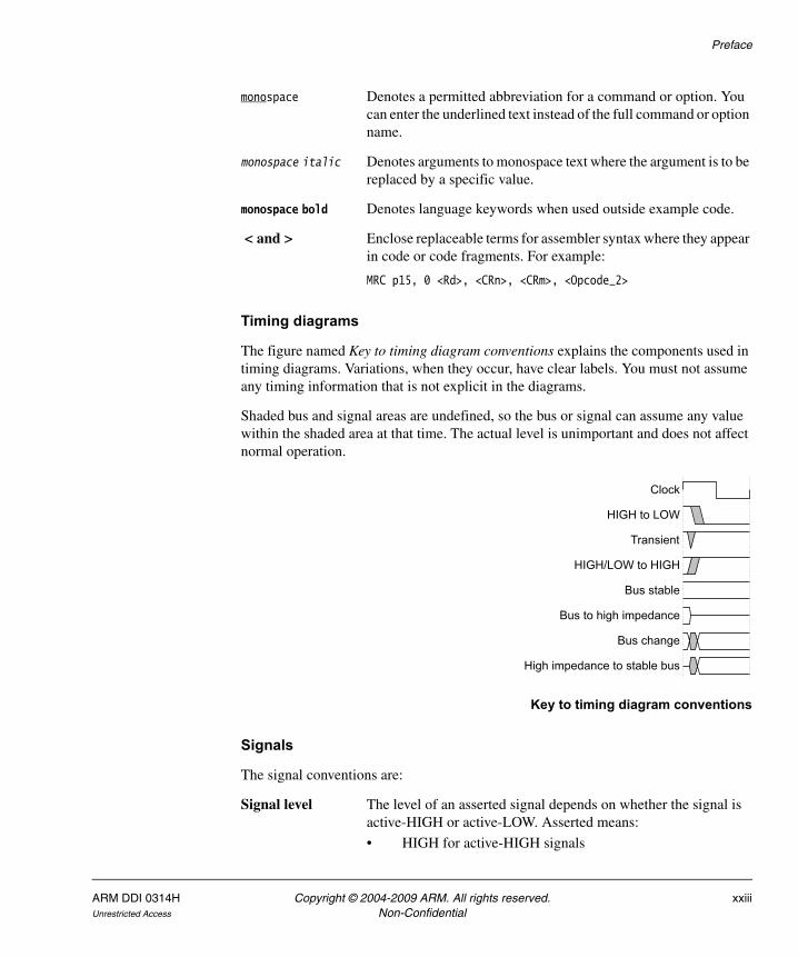
The figure named Key to timing diagram conventions explains the components used in timing diagrams. Variations, when they occur, have clear labels. You must not assume any timing information that is not explicit in the diagrams.
Shaded bus and signal areas are undefined, so the bus or signal can assume any value within the shaded area at that time. The actual level is unimportant and does not affect normal operation.
Key to timing diagram conventions
Signals
The signal conventions are:
Signal level The level of an asserted signal depends on whether the signal is active-HIGH or active-LOW. Asserted means:
• HIGH for active-HIGH signals
Clock
HIGH to LOW
Transient
HIGH/LOW to HIGH
Bus stable
Bus to high impedance
Bus change
High impedance to stable bus
ARM DDI 0314H Copyright © 2004-2009 ARM. All rights reserved. xxiiiUnrestricted Access Non-Confidential
Preface
• LOW for active-LOW signals.
Lower-case n At the start or end of a signal name denotes an active-LOW signal.
Further reading
This section lists publications by ARM and by third parties.
See Infocenter, http://infocenter.arm.com, for access to ARM documentation.
ARM publications
This document contains information that is specific to the CoreSight components. See the following documents for other relevant information:
• CoreSight Technology System Design Guide (ARM DGI 0012)
• CoreSight Architecture Specification (ARM IHI 0029)
• CoreSight Components Implementation Guide (ARM DII 0143)
• CoreSight DK9 Integration Manual (ARM DII 0131)
• CoreSight DK11 Integration Manual (ARM DII 0092)
• CoreSight DK-A8 Integration Manual (ARM DII 0135)
• CoreSight Serial Wire Debug Integration Manual (ARM DII 0095)
• CoreSight Serial Wire Viewer Integration Manual (ARM DII 0096)
• CoreSight ETM9 Technical Reference Manual (ARM DDI 0315)
• CoreSight ETM9 Implementation Guide (ARM DDI 0093)
• CoreSight ETM9 Integration Manual (ARM DII 0094)
• CoreSight ETM11 Technical Reference Manual (ARM DDI 0318)
• CoreSight ETM11 Implementation Guide (ARM DII 0097)
• CoreSight ETM11 Integration Manual (ARM DII 0098)
• ETM Architecture Specification (ARM IHI 0014)
• AMBA® AHB Trace Macrocell (HTM) Technical Reference Manual (ARM DDI 0328)
• Systems IP ARM11 AMBA (Rev 2.0) AHB Extensions (ARM IHI 0023)
xxiv Copyright © 2004-2009 ARM. All rights reserved. ARM DDI 0314HNon-Confidential Unrestricted Access
Preface
• AMBA 3 APB Protocol (ARM IHI 0024)
• ARM Architecture Reference Manual (ARM DDI 0406)
• ARM Debug Interface v5 Architecture Specification (ARM IHI 0031)
• ARM Debug Interface v5.1 Architecture Supplement (DSA09-PRDC-008772)
• RealView ICE User Guide (ARM DUI 0155).
ARM DDI 0314H Copyright © 2004-2009 ARM. All rights reserved. xxvUnrestricted Access Non-Confidential
Preface
FeedbackARM welcomes feedback on this product and its documentation.
Feedback on this product
If you have any comments or suggestions about this product, contact your supplier and give:
• The product name.
• The product revision or version.
• An explanation with as much information as you can provide. Include symptoms and diagnostic procedures if appropriate.
Feedback on content
If you have comments on content then send an e-mail to [email protected]. Give:
• the title
• the number, ARM DDI 0314H
• the page numbers to which your comments apply
• a concise explanation of your comments.
ARM also welcomes general suggestions for additions and improvements.
xxvi Copyright © 2004-2009 ARM. All rights reserved. ARM DDI 0314HNon-Confidential Unrestricted Access

Chapter 1 Introduction
This chapter contains an introduction to the CoreSight components. It contains the following sections:
• About the CoreSight components on page 1-2
• CoreSight block summary on page 1-4
• Typical CoreSight Design Kit debugging environment on page 1-5.
ARM DDI 0314H Copyright © 2004-2009 ARM. All rights reserved. 1-1Unrestricted Access Non-Confidential
Introduction
1.1 About the CoreSight componentsThe CoreSight components provide a multi-core debug and trace solution with high bandwidth for whole systems, including trace and monitor of the system bus.
1.1.1 Capabilities
The CoreSight components provide the following capabilities for system-wide trace:
• debug and trace visibility of whole systems
• cross triggering support between SoC subsystems
• multi-source trace in a single stream
• higher data compression than previous solutions
• standard programmer's models for standard tools support
• open interfaces for third party cores
• low pin count
• low silicon overhead.
1.1.2 Structure of the CoreSight Design Kit
The CoreSight components include the following:
Control and access components
Control and access components configure, access, and control the generation of trace. They do not generate trace, nor process the trace data. Examples include:
• Debug Access Port (DAP).
See Chapter 2 Debug Access Port.
• Embedded Cross Trigger (ECT).
See Chapter 4 Embedded Cross Trigger.
Sources Sources generate trace data for output through the AMBA Trace Bus (ATB). Examples include:
• AHB Trace Macrocell (HTM), documented separately.
See Further reading on page xxiv.
• CoreSight Embedded Trace Macrocells (ETMs), documented separately.
See Further reading on page xxiv.
• Instrumentation Trace Macrocell (ITM).
See Chapter 12 Instrumentation Trace Macrocell.
1-2 Copyright © 2004-2009 ARM. All rights reserved. ARM DDI 0314HNon-Confidential Unrestricted Access
Introduction
Links Links provide connection, triggering, and flow of trace data. Examples include:
• Synchronous 1:1 ATB bridge.
See Chapter 5 ATB 1:1 Bridge.
• Replicator.
See Chapter 6 ATB Replicator.
• Trace funnel.
See Chapter 7 CoreSight Trace Funnel.
Sinks Sinks are the end points for trace data on the SoC. Examples include:
• Trace Port Interface Unit (TPIU) for output of trace data off-chip.
See Chapter 8 Trace Port Interface Unit.
• Embedded Trace Buffer (ETB) for on-chip storage of trace data in RAM.
See Chapter 9 Embedded Trace Buffer.
• Serial Wire Output (SWO) for output of ITM trace through a single pin.
ARM DDI 0314H Copyright © 2004-2009 ARM. All rights reserved. 1-3Unrestricted Access Non-Confidential
Introduction
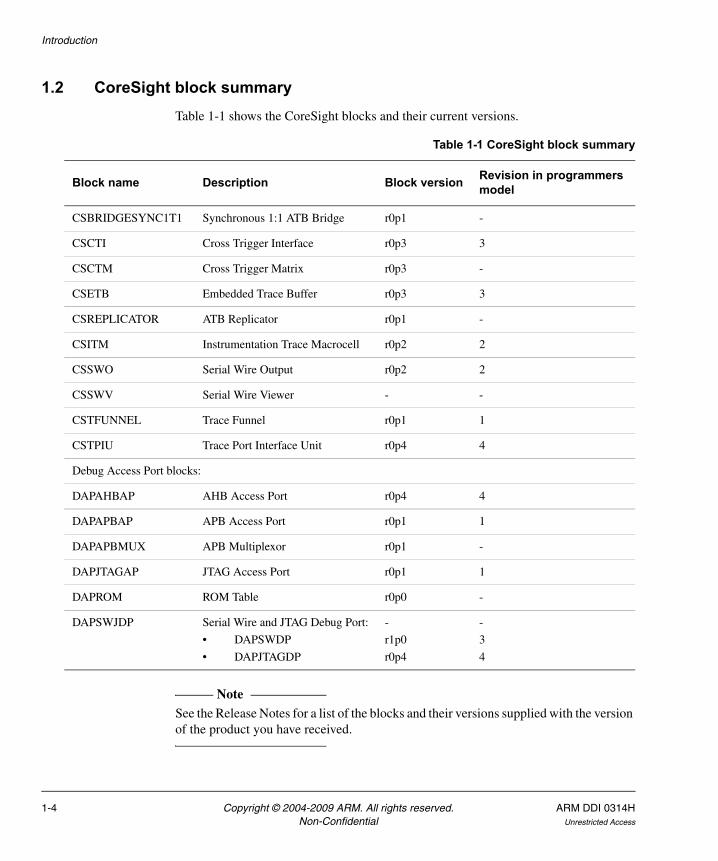
1.2 CoreSight block summaryTable 1-1 shows the CoreSight blocks and their current versions.
Note See the Release Notes for a list of the blocks and their versions supplied with the version of the product you have received.
Table 1-1 CoreSight block summary
Block name Description Block version Revision in programmers model
CSBRIDGESYNC1T1 Synchronous 1:1 ATB Bridge r0p1 -
CSCTI Cross Trigger Interface r0p3 3
CSCTM Cross Trigger Matrix r0p3 -
CSETB Embedded Trace Buffer r0p3 3
CSREPLICATOR ATB Replicator r0p1 -
CSITM Instrumentation Trace Macrocell r0p2 2
CSSWO Serial Wire Output r0p2 2
CSSWV Serial Wire Viewer - -
CSTFUNNEL Trace Funnel r0p1 1
CSTPIU Trace Port Interface Unit r0p4 4
Debug Access Port blocks:
DAPAHBAP AHB Access Port r0p4 4
DAPAPBAP APB Access Port r0p1 1
DAPAPBMUX APB Multiplexor r0p1 -
DAPJTAGAP JTAG Access Port r0p1 1
DAPROM ROM Table r0p0 -
DAPSWJDP Serial Wire and JTAG Debug Port:
• DAPSWDP
• DAPJTAGDP
-
r1p0
r0p4
-
3
4
1-4 Copyright © 2004-2009 ARM. All rights reserved. ARM DDI 0314HNon-Confidential Unrestricted Access
Introduction
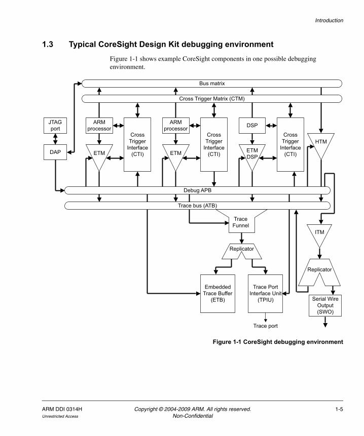
1.3 Typical CoreSight Design Kit debugging environmentFigure 1-1 shows example CoreSight components in one possible debugging environment.
Figure 1-1 CoreSight debugging environment
Bus matrix
Cross Trigger Matrix (CTM)
JTAG port
DAP
ARM processor
ARM processor DSP
Debug APB
Trace bus (ATB)
TraceFunnel
Replicator
Cross Trigger
Interface (CTI)
Cross Trigger
Interface (CTI)
Cross Trigger
Interface (CTI)ETM ETM ETM
DSP
HTM
Embedded Trace Buffer
(ETB)
Trace Port Interface Unit
(TPIU)
Trace port
ITM
Replicator
Serial Wire Output (SWO)
ARM DDI 0314H Copyright © 2004-2009 ARM. All rights reserved. 1-5Unrestricted Access Non-Confidential

Introduction
1-6 Copyright © 2004-2009 ARM. All rights reserved. ARM DDI 0314HNon-Confidential Unrestricted Access
Chapter 2 Debug Access Port
This chapter describes the Debug Access Port (DAP). The DAP provides multiple master driving ports, all accessible and controlled through a single external interface port to provide system-wide debug. The chapter contains the following sections:
• About the Debug Access Port on page 2-2
• SWJ-DP on page 2-9
• JTAG-DP on page 2-14
• SW-DP on page 2-16
• Common debug port features and registers on page 2-24
• Access ports on page 2-38
• AHB-AP on page 2-39
• APB-AP on page 2-51
• JTAG-AP on page 2-59
• Auxiliary Access Port on page 2-65
• APB multiplexor on page 2-66
• ROM table on page 2-72
• Authentication requirements for Debug Access Port on page 2-74
• Clocks, power, and resets on page 2-75.
ARM DDI 0314H Copyright © 2004-2009 ARM. All rights reserved. 2-1Unrestricted Access Non-Confidential
Debug Access Port
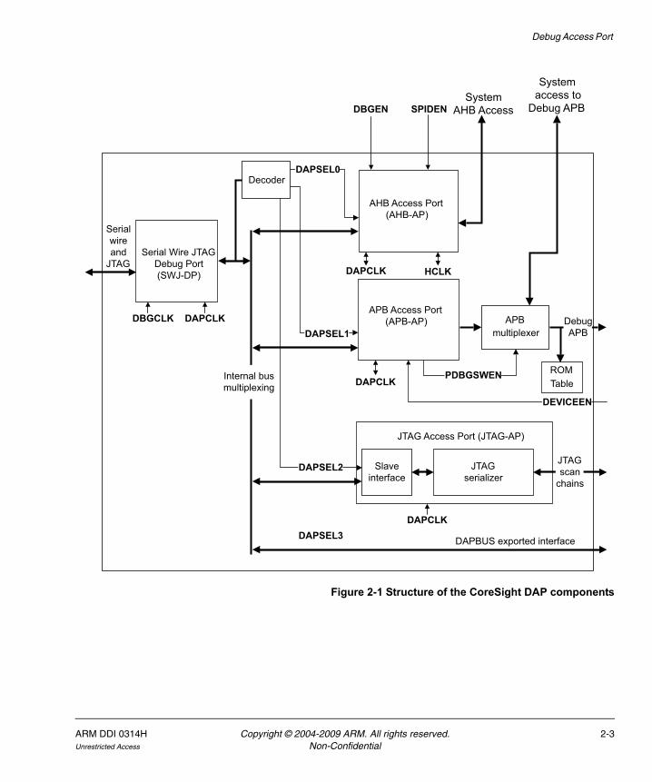
2.1 About the Debug Access PortThe Debug Access Port (DAP) is an implementation of an ARM Debug Interface version 5.1 (ADIv5.1) comprising a number of components supplied in a single configuration. All the supplied components fit into the various architectural components for Debug Ports (DPs), which are used to access the DAP from an external debugger and Access Ports (APs), to access on-chip system resources.
The debug port and access ports together are referred to as the DAP.
The DAP provides real-time access for the debugger without halting the processor to:
• AMBA system memory and peripheral registers
• All debug configuration registers.
The DAP also provides debugger access to JTAG scan chains of system components, for example non-CoreSight compliant processors. Figure 2-1 on page 2-3 shows the top-level view of the functional blocks of the DAP. Figure 2-2 on page 2-4, Figure 2-3 on page 2-4, and Figure 2-4 on page 2-5 show separate components in more detail.
2-2 Copyright © 2004-2009 ARM. All rights reserved. ARM DDI 0314HNon-Confidential Unrestricted Access
Debug Access Port
Figure 2-1 Structure of the CoreSight DAP components
Decoder
HCLK
DBGEN SPIDEN
DEVICEEN
Internal busmultiplexing
SystemAHB Access
APBmultiplexer
Systemaccess to
Debug APB
AHB Access Port (AHB-AP)
Slave interface
JTAGserializer
DAPCLK
JTAG Access Port (JTAG-AP)
APB Access Port (APB-AP)
JTAGscan
chains
DAPCLK
DAPCLK
PDBGSWEN
DebugAPB
ROMTable
Serial Wire JTAG Debug Port (SWJ-DP)
DAPSEL0
DAPSEL1DAPCLKDBGCLK
DAPSEL2
Serial wire and
JTAG
DAPSEL3 DAPBUS exported interface
ARM DDI 0314H Copyright © 2004-2009 ARM. All rights reserved. 2-3Unrestricted Access Non-Confidential

Debug Access Port
Figure 2-2 SWJ Debug Port
Figure 2-3 AHB Access Port
Controlregisters
Masterinterface
Debug power on requestSystem power on request
Debug reset request
Serial Wire JTAG Debug Port (SWJ-DP)
JTAGinterface
DAPCLKDBGCLK
SWinterface
Serial wire and
JTAG
SWJ-DP select
HCLK
DBGEN SPIDENSystem
AHB Access
AHB Access Port (AHB-AP)
AHB master
interface
AHBaccesscontrol
DAPCLK
Slave interface
DAPSEL0
SWJ-DP
2-4 Copyright © 2004-2009 ARM. All rights reserved. ARM DDI 0314HNon-Confidential Unrestricted Access

Debug Access Port
Figure 2-4 APB Access Port
The DAP enables debug access to the complete SoC using a number of master ports. Access to the CoreSight Debug Advanced Peripheral Bus (APB) is enabled through the APB Access Port (APB-AP) and APB Multiplexor (APB-MUX), and system access through the Advanced High-performance Bus Access Port (AHB-AP).
The DAP comprises the following interface blocks:
• External debug access using the Serial Wire JTAG Debug Port (SWJ-DP). The SWJ-DP enables selection of:
— external serial wire access using the Serial Wire Debug Port (SW-DP)
— external JTAG access using the JTAG Debug Port (JTAG-DP)
— a Dormant state which disables the Serial Wire interface to enable the connection to be shared with other protocols.
• System access using:
— AHB-AP
— APB-AP
— JTAG-AP
— DAPBUS exported interface.
• An APB multiplexor enables system access to CoreSight components connected to the Debug APB.
• The ROM table provides a list of memory locations of CoreSight components connected to the Debug APB. This is visible from both tools and system access. The ROM table indicates the position of all CoreSight components in a system and assists in topology detection. See the CoreSight Architecture Specification for more information on topology detection. For more information about the ROM Table, see ROM table on page 2-72.
APB master
interface
APBaccesscontrol
APB Access Port (APB-AP)
DAPCLK
DEVICEEN
PDBGSWEN
Slave interface
DAPSEL1
SWJ-DP
ARM DDI 0314H Copyright © 2004-2009 ARM. All rights reserved. 2-5Unrestricted Access Non-Confidential
Debug Access Port
The debug port supplied with the DAP is:
Serial Wire and JTAG Debug Port (SWJ-DP)
This is a combined debug port which can communicate in either JTAG or Serial Wire protocols as defined in ADIv5.1. It contains two debug ports, the SW-DP and the JTAG-DP that you can select through an interface sequence to move between debug port interfaces.
The JTAG-DP is compliant with DP architecture version 0. The SW-DP is compliant with DP architecture version 2 and Serial Wire protocol version 2, which enable an SW-DP to share a target connection with other SW-DPs or other components implementing different protocols.
The access ports specified for CoreSight are:
AHB Access Port (AHB-AP)
The AHB-AP provides an AHB-Lite master for access to a system AHB bus. This is compliant with the Memory Access Port (MEM-AP) in ADIv5.1 and can perform 8 to 32-bit accesses.
APB Access Port (APB-AP)
The APB-AP provides an APB master in AMBA v3.0 for access to the Debug APB bus. This is compliant with the MEM-AP with a fixed transfer size of 32-bits.
JTAG Access Port (JTAG-AP)
The JTAG-AP provides JTAG access to on-chip components, operating as a JTAG master port to drive JTAG chains throughout the ASIC. This is an implementation of the JTAG-AP in ADIv5.1.
The DAP also implements a DAPBUS interface to enable an additional access port to be connected externally for connection to certain processors.
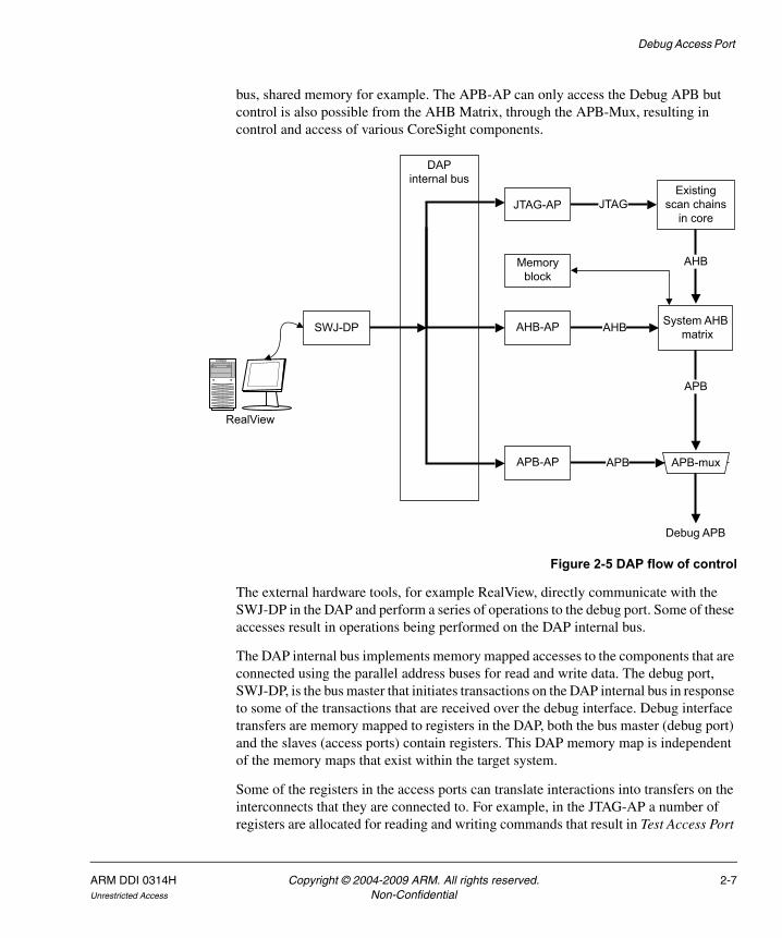
2.1.1 DAP flow of control
Figure 2-5 on page 2-7 shows the flow of control for the DAP when used with an off-chip debugging unit such as RealView ICE.
The DAP, as a whole, acts as a component to translate data transfers from one type of interface, the external JTAG or serial wire link from tools, to different internal transactions. The debug port receives JTAG or serial wire transfers but controls the JTAG-AP, AHB-AP, and APB-AP through a standard bus interface. JTAG-AP receives these bus transactions and translates them into JTAG instructions for control of any connected TAP controllers such as a processor. The AHB-AP is a bus master, along with any connected cores, on the system AHB Matrix that can access slaves connected to that
2-6 Copyright © 2004-2009 ARM. All rights reserved. ARM DDI 0314HNon-Confidential Unrestricted Access
Debug Access Port
bus, shared memory for example. The APB-AP can only access the Debug APB but control is also possible from the AHB Matrix, through the APB-Mux, resulting in control and access of various CoreSight components.
Figure 2-5 DAP flow of control
The external hardware tools, for example RealView, directly communicate with the SWJ-DP in the DAP and perform a series of operations to the debug port. Some of these accesses result in operations being performed on the DAP internal bus.
The DAP internal bus implements memory mapped accesses to the components that are connected using the parallel address buses for read and write data. The debug port, SWJ-DP, is the bus master that initiates transactions on the DAP internal bus in response to some of the transactions that are received over the debug interface. Debug interface transfers are memory mapped to registers in the DAP, both the bus master (debug port) and the slaves (access ports) contain registers. This DAP memory map is independent of the memory maps that exist within the target system.
Some of the registers in the access ports can translate interactions into transfers on the interconnects that they are connected to. For example, in the JTAG-AP a number of registers are allocated for reading and writing commands that result in Test Access Port
AHB
SWJ-DP
DAPinternal bus
Existing scan chains
in coreJTAGJTAG-AP
APB
Debug APB
APB-AP
AHBAHB-AP System AHB matrix
APB
APB-mux
RealView
Memoryblock
ARM DDI 0314H Copyright © 2004-2009 ARM. All rights reserved. 2-7Unrestricted Access Non-Confidential

Debug Access Port
(TAP) instructions on connected devices, for example cores. The processor is also a bus master on a system memory structure to which the AHB-AP has access, so both the processor and AHB-AP have access to shared memory devices, or other bus slave components.
2-8 Copyright © 2004-2009 ARM. All rights reserved. ARM DDI 0314HNon-Confidential Unrestricted Access
Debug Access Port
2.2 SWJ-DPThe SWJ-DP is a combined JTAG-DP and SW-DP that enables you to connect either a Serial Wire Debug (SWD) or JTAG probe to a target. It is the standard CoreSight debug port, and enables access either to the JTAG-DP or SW-DP blocks. To make efficient use of package pins, serial wire shares, or overlays, the JTAG pins use an autodetect mechanism that switches between JTAG-DP and SW-DP depending on which probe is connected. A special sequence on the SWDIOTMS pin is used to switch between JTAG-DP and SW-DP. When the switching sequence has been transmitted to the SWJ-DP, it behaves as a dedicated JTAG-DP or SW-DP depending upon which sequence had been performed.
Note For more information about the programming capabilities and features of the SWJ-DP, see the JTAG-DP and SW-DP sections in JTAG-DP on page 2-14 and SW-DP on page 2-16.
Figure 2-6 on page 2-10 shows the external connections to the SWJ-DP.
The SWJ-DP is described in:
• Structure of the SWJ-DP on page 2-10
• Operation of the SWJ-DP on page 2-10
• JTAG and SWD interface on page 2-11
• Clock, reset and power domain support on page 2-12
• SWD and JTAG selection mechanism on page 2-12.
ARM DDI 0314H Copyright © 2004-2009 ARM. All rights reserved. 2-9Unrestricted Access Non-Confidential

Debug Access Port
Figure 2-6 SWJ-DP external connections
2.2.1 Structure of the SWJ-DP
The SWJ-DP consists of a wrapper around the JTAG-DP and SW-DP. It selects JTAG or SWD as the connection mechanism and enables either JTAG-DP or SW-DP as the interface to the DAP.
2.2.2 Operation of the SWJ-DP
SWJ-DP enables you to design an Application Specific Integrated Circuit (ASIC) that you can use in systems that require either a JTAG interface or a SWD interface. There is a trade-off between the number of pins used and compatibility with existing hardware and test equipment. There are several scenarios where you must use a JTAG debug interface. These enable:
• inclusion in an existing scan chain, usually on-chip TAPs used for test or other purposes.
• the device to be cascaded with legacy devices that use JTAG for debug
SWD/JTAG select
TDOTDI
nTRST
TCK
TMSnPOTRST
JTAG-DP
DBGDI
DBGDO
DBGDOEN
DBGCLK
DBGRESETn
SW-DP
From power-on reset
nPOTRST
SWCLKTCK
TRACESWO
TDO
TDI
SWDIOTMS
nTRST
TDOTDI
nTRST
SWDITMS
SWDO
SWDOEN
SWCLKTCK
SWJ-DP
2-10 Copyright © 2004-2009 ARM. All rights reserved. ARM DDI 0314HNon-Confidential Unrestricted Access
Debug Access Port
• use of existing debug hardware with the corresponding test TAPs, for example in Automatic Test Equipment (ATE).
You can connect an ASIC fitted with SWJ-DP support to legacy JTAG equipment without making any changes. If an SWD tool is available, only two pins are required, instead of the usual four used for JTAG. You can therefore use the other two pins for something else.
You can only use these two pins if there is no conflict with their use in JTAG mode. To support use of SWJ-DP in a scan chain with other JTAG devices, the default state after reset must be to use these pins for their JTAG function. If the direction of the alternative function is compatible with being driven by a JTAG debug device, the transition to a shift state can be used to transition from the alternative function to JTAG mode. You cannot use the other function while the ASIC is in JTAG debug mode.
The switching scheme is arranged so that, provided there is no conflict on the TDI and TDO pins, a JTAG debugger can connect by sending a specific sequence. The connection sequence used for SWD is safe when applied to the JTAG interface, even if hot-plugged, enabling the debugger to continually retry its access sequence. A sequence with TMS=1 ensures that JTAG-DP, SW-DP, and the watcher circuit are in a known reset state. The pattern used to select SWD has no effect on JTAG targets. SWJ-DP is compatible with a free-running TCK, or a gated clock supplied by external tools.
2.2.3 JTAG and SWD interface
The external JTAG interface has four mandatory pins, TCK, TMS, TDI, and TDO, and an optional reset, nTRST. JTAG-DP and SW-DP also require a separate power-on reset, nPOTRST.
The external SWD interface requires two pins:
• a bidirectional SWDIO signal
• a clock, SWCLK, which can be input or output from the device.
The block level interface has two pins for data plus an output enable that must be used to drive a bidirectional pad for the external interface, and clock and reset signals. To enable sharing of the connector for either JTAG or SWD, connections must be made external to the SWJ-DP block, as shown in Figure 2-6 on page 2-10. In particular, TMS must be a bidirectional pin to support the bidirectional SWDIO pin in SWD mode. When SWD mode is used, the TDO pin is expected to be re-used for Serial Wire Output (SWO). You can use the TDI pin as an alternative input function.
Note If you require SWO functionality in JTAG mode, you must have a dedicated pin for TRACESWO.
ARM DDI 0314H Copyright © 2004-2009 ARM. All rights reserved. 2-11Unrestricted Access Non-Confidential
Debug Access Port
2.2.4 Clock, reset and power domain support
In the SWCLKTCK clock domain, there are registers to enable power control for the on-chip debug infrastructure. This enables the majority of the debug logic, such as ETM and ETB, to be powered down by default, and only the serial engine has to be clocked. A debug session then starts by powering up the remainder of the debug components. In SWJ-DP, either JTAG-DP or SW-DP can make power-up or reset requests but only if they are the selected device. Even in a system which does not provide a clock and reset control interface to the DAP, it is necessary to connect these signals so it appears that a clock and reset controller is present. This permits correct handshaking of the request and acknowledge signals.
To help provide separate power domains, it is possible to partition the RTL of SWJ-DP to enable an always on domain and debug domain as defined in ADIv5.1. Figure 2-7 shows the RTL structure to support power domain structure.
Figure 2-7 SWJ-DP signal clamping
2.2.5 SWD and JTAG selection mechanism
SWJ-DP enables one of the following modes to be selected:
• JTAG protocol
• Serial Wire Debug protocol
• Dormant.
DAPSwDpProtocol
DAPJtagDpProtocol
DAPSwjwatcher DAPDpIMux
DAPSwDpSync
DAPDpApbSync
DAPDpApbIfClamp
To/from JTAG/SW interface
To/from DAP internal busnCDBGPWRDN
DAPSwDpApbIf
2-12 Copyright © 2004-2009 ARM. All rights reserved. ARM DDI 0314HNon-Confidential Unrestricted Access
Debug Access Port
When in Dormant mode, the TMS, TDI, and TDO signals can be used for other purposes, enabling alternative debug protocols to be used by other devices connected to the same pins.
The switcher defaults to JTAG operation on power-on reset, therefore the JTAG protocol can be used from reset without sending a selection sequence.
The SWJ-DP contains a mode status output, JTAGNSW, that is HIGH when the SWJ-DP is in JTAG mode and LOW when in SWD or Dormant mode. This signal can be used to:
• disable other TAP controllers when the SWJ-DP is in SWD or Dormant mode, for example by disabling TCK or forcing TMS HIGH
• multiplex the Serial Wire output, TRACESWO, onto another pin such as TDO when not in JTAG mode.
Another status output, JTAGTOP, indicates the state of the JTAG-DP TAP controller. These states are:
• Test-Logic-Reset
• Run-Test/Idle
• Select-DR-Scan
• Select-IR-Scan.
This signal can be used with JTAGNSW to control multiplexers so that, for example, TDO and TDI can be reused as General Purpose Input/Output (GPIO) signals when the device is not in JTAG mode, or during cycles when these signals are not in use by the JTAG-DP TAP controller.
See the ARM Debug Interface v5 Architecture Specification and the ARM Debug Interface v5.1 Architecture Supplement for information on the SWJ-DP switching sequences.
ARM DDI 0314H Copyright © 2004-2009 ARM. All rights reserved. 2-13Unrestricted Access Non-Confidential

Debug Access Port
2.3 JTAG-DPThe JTAG-DP supplied with the DAP is an implementation of the JTAG-DP defined in ADIv5.1, which also contains a detailed explanation of its programmers model, capabilities and features.
JTAG-DP contains a debug port state machine (JTAG) that controls the JTAG-DP operation, including controlling the scan chain interface that provides the external physical interface to the JTAG-DP. It is based closely on the JTAG TAP State Machine, see IEEE Std 1149.1-2001.
This section contains the following:
• Overview
• Implementation specific details.
2.3.1 Overview
With the JTAG-DP, IEEE 1149.1 scan chains are used to read or write register information. A pair of scan chain registers is used to access the main control and access registers within the Debug Port:
• DPACC used for Debug Port (DP) accesses.
• APACC used for Access Port (AP) accesses. An APACC access might access a register of a debug component of the system to which the interface is connected.
The scan chain model implemented by a JTAG-DP has the concepts of capturing the current value of APACC or DPACC, and of updating APACC or DPACC with a new value. An update might cause a read or write access to a DAP register that might then cause a read or write access to a debug register of a connected debug component. The operations available on JTAG-DP are described in the ARM Debug Interface v5 Architecture Specification and the ARM Debug Interface v5.1 Architecture Supplement. The implemented registers present within the supplied JTAG-DP are described in Implementation specific details.
2.3.2 Implementation specific details
The implementation specific details are described in:
• Physical interface on page 2-15
• Programmers model on page 2-15.
2-14 Copyright © 2004-2009 ARM. All rights reserved. ARM DDI 0314HNon-Confidential Unrestricted Access
Debug Access Port
Physical interface
Table 2-1 shows the physical interface for JTAG-DP and the relationship to the signal references in ADIv5.1. The interface does not include a return clock signal. RTCK and the nTRST signals are optional because this only relates to resetting the DBGTAP state machine which can be performed by transmitting 5 TCK pulses with TMS HIGH.
Programmers model
Table 2-2 lists all implemented registers accessible by JTAG-DP. All other IR instructions are implemented as BYPASS and an external TAP controller must be implemented in accordance with ADIv5.1 if more IR registers are required, for example JTAG TAP boundary scan.
For more information about these registers, their features, and how to access them, see the ARM Debug Interface v5 Architecture Specification and the ARM Debug Interface v5.1 Architecture Supplement. Implementation specific detail is described in Common debug port features and registers on page 2-24.
Table 2-1 JTAG-DP physical interface
Implementation signal name (JTAG-DP) ADIv5.1 signal name (JTAG-DP) Type JTAG-DP signal description
TDI DBGTDI Input Debug Data In
TDO DBGTDO Output Debug Data Out
SWCLKTCK TCK Input Debug Clock
SWDITMS DBGTMS Input Debug Mode Select
nTRST DBGTRSTn Input Debug TAP Reset
Table 2-2 JTAG-DP registers
IR instruction value JTAG-DP register DR scan width Description
b1000 ABORT 35 JTAG-DP Abort Register (ABORT)
b1010 DPACC 35 JTAG DP/AP Access Registers (DPACC/APACC)
b1011 APACC 35
b1110 IDCODE 32 JTAG Device ID Code Register (IDCODE)
b1111 BYPASS 1 JTAG Bypass Register (BYPASS)
ARM DDI 0314H Copyright © 2004-2009 ARM. All rights reserved. 2-15Unrestricted Access Non-Confidential
Debug Access Port
2.4 SW-DPThis section briefly describes the Serial Wire Debug Port (SW-DP) interface. This implementation is taken from ADIv5.1 and operates with a synchronous serial interface. This uses a single bidirectional data signal, and a clock signal.
2.4.1 Overview
The SW-DP provides a low pin count bi-directional serial connection to the DAP with a reference clock signal for synchronous operation.
Communications with the SW-DP use a three-phase protocol:
• A host-to-target packet request.
• A target-to-host acknowledge response.
• A data transfer phase, if required. This can be target-to-host or host-to-target, depending on the request made in the first phase.
A packet request from a debugger indicates whether the required access is to a DP register (DPACC) or to an AP register (APACC), and includes a two-bit register address. The protocol is described in detail in the ARM Debug Interface v5 Architecture Specification and the ARM Debug Interface v5.1 Architecture Supplement.
2.4.2 Implementation specific details
This section contains the following:
• Clocking
• Overview of debug interface on page 2-17.
Clocking
The SW-DP clock, SWCLKTCK, can be asynchronous to the DAPCLK. SWCLKTCK can be stopped when the debug port is idle.
The host must continue to clock the interface for a number of cycles after the data phase of any data transfer. This ensures that the transfer can be clocked through the SW-DP. This means that after the data phase of any transfer the host must do one of the following:
• immediately start a new SW-DP operation
• continue to clock the SW-DP serial interface until the host starts a new SW-DP operation
2-16 Copyright © 2004-2009 ARM. All rights reserved. ARM DDI 0314HNon-Confidential Unrestricted Access
Debug Access Port
• after clocking out the data parity bit, continue to clock the SW-DP serial interface until it has clocked out at least 8 more clock rising edges, before stopping the clock.
Overview of debug interface
This section gives an overview of the physical interface used by the SW-DP.
Line interface
The SW-DP uses a serial wire for both host and target sourced signals. The host emulator drives the protocol timing - only the host emulator generates packet headers.
The SW-DP operates in synchronous mode, and requires a clock pin and a data pin.
Synchronous mode uses a clock reference signal, which can be sourced from an on-chip source and exported, or provided by the host device. This clock is then used by the host as a reference for generation and sampling of data so that the target is not required to perform any oversampling.
Both the target and host are capable of driving the bus HIGH and LOW, or tristating it. The ports must be able to tolerate short periods of contention to allow for loss of synchronization.
Line pullup
Both the host and target are able to drive the line HIGH or LOW, so it is important to ensure that contention does not occur by providing undriven time slots as part of the handover. So that the line can be assumed to be in a known state when neither is driving the line, a 100kΩ pullup is required at the target, but this can only be relied on to maintain the state of the wire. If the wire is driven LOW and released, the pullup resistor eventually brings the line to the HIGH state, but this takes many bit periods.
The pullup is intended to prevent false detection of signals when no host device is connected. It must be of a high value to reduce IDLE state current consumption from the target when the host actively pulls down the line.
Note Whenever the line is driven LOW, this results in a small current drain from the target. If the interface is left connected for extended periods when the target has to use a low power mode, the line must be held HIGH, or reset, by the host until the interface must be activated.
ARM DDI 0314H Copyright © 2004-2009 ARM. All rights reserved. 2-17Unrestricted Access Non-Confidential

Debug Access Port
Line turn-round
To avoid contention, a turnaround period is required when the device driving the wire changes.
Idle and reset
Between transfers, the host must either drive the line LOW to the IDLE state, or continue immediately with the start bit of a new transfer. The host is also free to leave the line HIGH, either driven or tristated, after a packet. This reduces the static current drain, but if this approach is used with a free running clock, a minimum of 50 clock cycles must be used, followed by a READ-ID as a new re-connection sequence.
There is no explicit reset signal for the protocol. A reset is detected by either host or target when the expected protocol is not observed. It is important that both ends of the link become reset before the protocol can be restarted with a reconnection sequence. Re-synchronization following the detection of protocol errors or after reset is achieved by providing 50 clock cycles with the line HIGH, or tristate, followed by a read ID request.
If the SW-DP detects that it has lost synchronization, for example if no stop bit is seen when expected, it leaves the line undriven and waits for the host to either re-try with a new header after a minimum of one cycle with the line LOW, or signals a reset by not driving the line itself. If the SW-DP detects two bad data sequences in a row, it locks out until a reset sequence of 50 clock cycles with DBGDI HIGH is seen.
If the host does not see an expected response from SW-DP, it must allow time for SW-DP to return a data payload. The host can then retry with a read to the SW-DP ID code register. If this is unsuccessful, the host must attempt a reset.
2.4.3 Transfer timings
This section describes the interaction between the timing of transactions on the serial wire interface, and the DAP internal bus transfers. It shows when the target responds with a WAIT acknowledgement.
Figure 2-8 on page 2-19 shows the effect of signalling ACK = WAIT on the length of the packet.
2-18 Copyright © 2004-2009 ARM. All rights reserved. ARM DDI 0314HNon-Confidential Unrestricted Access
Debug Access Port
Figure 2-8 SW-DP acknowledgement timing
An access port access results in the generation of a transfer on the DAP internal bus. These transfers have an address phase and a data phase. The data phase can be extended by the access if it requires extra time to process the transaction, for example, if it has to perform an AHB access to the system bus to read data.
Table 2-3 shows the terms used in Figure 2-9 on page 2-20 to Figure 2-11 on page 2-21.
Figure 2-9 on page 2-20 shows a sequence of write transfers. It shows that a single new transfer, WD[1], can be accepted by the serial engine, while a previous write transfer, WD[0], is completing. Any subsequent transfer must be stalled until the first transfer completes.
Write W 00 P O W 00 P O0 1 0Z Z Z 01 0 Z WDATA[31:0] P13 bits for rejected packet 46 bits for accepted packet
Read R 00 P O R 00 P O0 1 0Z Z Z 01 0 ZRDATA[31:0] P
ACK=010: Wait ACK=100: Accept
ST DP ST DP DP
ST AP
P1
P1 ST AP
P1
Table 2-3 Terms used in SW-DP timing
Term Description
W.APACC Write a DAP access port register.
R.APACC Read a DAP access port register.
xxPACC Read or write, to debug port or access port register.
WD[0] First write packet data.
WD[-1] Previous write packet data. A transaction that happened before this timeframe.
WD[1] Second write packet data.
RD[0] First read packet data.
RD[1] Second read packet data.
ARM DDI 0314H Copyright © 2004-2009 ARM. All rights reserved. 2-19Unrestricted Access Non-Confidential
Debug Access Port
Figure 2-9 SW-DP to DAP bus timing for write
Figure 2-10 shows a sequence of read transfers. It shows that the payload for an access port read transfer provides the data for the previous read request. A read transfer only stalls if the previous transfer has not completed, therefore the first read transfer returns undefined data. It is still necessary to return data to ensure that the protocol timing remains predictable.
Figure 2-10 SW-DP to DAP bus timing for read
Figure 2-11 on page 2-21 shows a sequence of transfers separated by IDLE periods. It shows that the wire is always handed back to the host after any transfer.
T OK T WD[0] T OK T WD[1] xxPACC T T T OK TSW
WD[-1] WD[0] WD[1]
Access [0] Access[1]
Access[0] accepted and buffered
Access[1] accepted and buffered
Access[2] rejecteduntil Access[1]
completes
Access[0] presented to DAP internal bus
A[0] A[1]
WD[0] WD[0]
Buffer empty before end of header
DAP bus
DAP READY
HADDR
HWDATA
HREADY
W.APACC W.APACC Wait xxPACC
T OK RD[-1] T OK RD[0] xxPACC T T xxPACC T OK TSW
RD[0] RD[1]
A[0] A[1]
RD[0] RD[1]
DAP bus
DAP READY
HADDR
HWDATA
HREADY
T
RD[0] RD[0]DP read buffer
R.APACC[0] R.APACC[1] Wait
2-20 Copyright © 2004-2009 ARM. All rights reserved. ARM DDI 0314HNon-Confidential Unrestricted Access
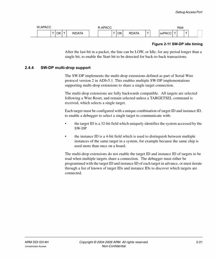
Debug Access Port
Figure 2-11 SW-DP idle timing
After the last bit in a packet, the line can be LOW, or Idle, for any period longer than a single bit, to enable the Start bit to be detected for back-to-back transactions.
2.4.4 SW-DP multi-drop support
The SW-DP implements the multi-drop extensions defined as part of Serial Wire protocol version 2 in ADIv5.1. This enables multiple SW-DP implementations supporting multi-drop extensions to share a single target connection.
The multi-drop extensions are fully backwards compatible. All targets are selected following a Wire Reset, and remain selected unless a TARGETSEL command is received, which selects a single target.
Each target must be configured with a unique combination of target ID and instance ID, to enable a debugger to select a single target to communicate with:
• the target ID is a 32-bit field which uniquely identifies the system accessed by the SW-DP
• the instance ID is a 4-bit field which is used to distinguish between multiple instances of the same target in a system, for example because the same chip is used more than once on a board.
The multi-drop extensions do not enable the target ID and instance ID of targets to be read when multiple targets share a connection. The debugger must either be programmed with the target ID and instance ID of each target in advance, or must iterate through a list of known of target IDs and instance IDs to discover which targets are connected.
T OK T WDATA T OK RDATA T xxPACC T T
W.APACC R.APACC Wait
ARM DDI 0314H Copyright © 2004-2009 ARM. All rights reserved. 2-21Unrestricted Access Non-Confidential
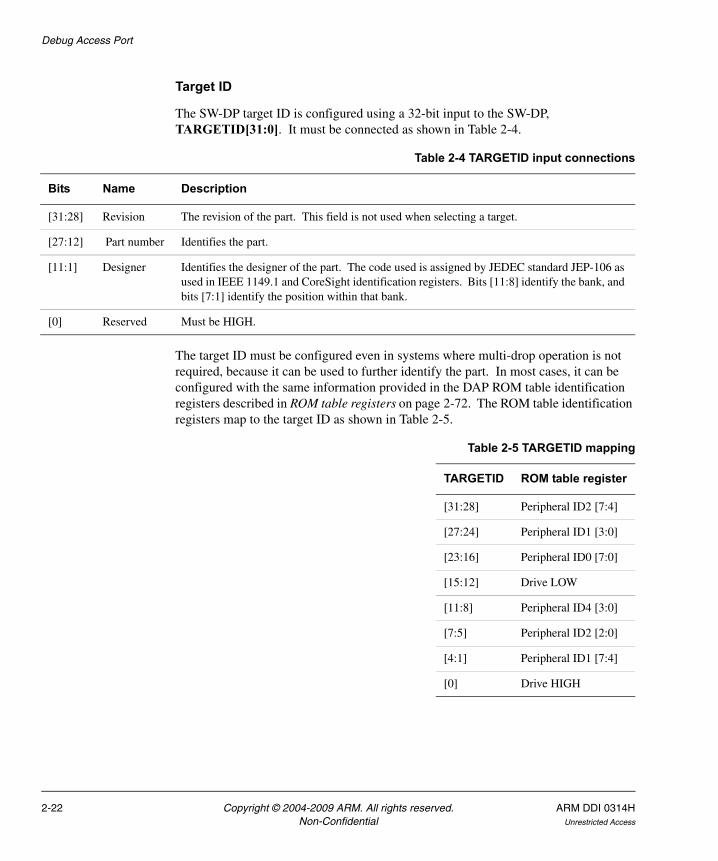
Debug Access Port
Target ID
The SW-DP target ID is configured using a 32-bit input to the SW-DP, TARGETID[31:0]. It must be connected as shown in Table 2-4.
The target ID must be configured even in systems where multi-drop operation is not required, because it can be used to further identify the part. In most cases, it can be configured with the same information provided in the DAP ROM table identification registers described in ROM table registers on page 2-72. The ROM table identification registers map to the target ID as shown in Table 2-5.
Table 2-4 TARGETID input connections
Bits Name Description
[31:28] Revision The revision of the part. This field is not used when selecting a target.
[27:12] Part number Identifies the part.
[11:1] Designer Identifies the designer of the part. The code used is assigned by JEDEC standard JEP-106 as used in IEEE 1149.1 and CoreSight identification registers. Bits [11:8] identify the bank, and bits [7:1] identify the position within that bank.
[0] Reserved Must be HIGH.
Table 2-5 TARGETID mapping
TARGETID ROM table register
[31:28] Peripheral ID2 [7:4]
[27:24] Peripheral ID1 [3:0]
[23:16] Peripheral ID0 [7:0]
[15:12] Drive LOW
[11:8] Peripheral ID4 [3:0]
[7:5] Peripheral ID2 [2:0]
[4:1] Peripheral ID1 [7:4]
[0] Drive HIGH
2-22 Copyright © 2004-2009 ARM. All rights reserved. ARM DDI 0314HNon-Confidential Unrestricted Access
Debug Access Port
Instance ID
The SW-DP instance ID is configured using a 4-bit input to the SW-DP, INSTANCEID[3:0]. If multiple targets with the same target ID might share a connection, INSTANCEID must be driven differently for each target, for example by using nonvolatile storage configured differently for each target.
In most cases, this input can be driven LOW.
ARM DDI 0314H Copyright © 2004-2009 ARM. All rights reserved. 2-23Unrestricted Access Non-Confidential

Debug Access Port
2.5 Common debug port features and registersThis section describes specific details of features and registers that are present within this implementation of SW-DP and JTAG-DP as part of the SWJ-DP. For all the features and registers present within SW-DP and JTAG-DP, see the ARM Debug Interface v5 Architecture Specification and the ARM Debug Interface v5.1 Architecture Supplement. This section contains the following implementation specific details:
• Features overview
• Example pushed operations
• Debug Port registers overview on page 2-26
• Implementation specific registers on page 2-26.
2.5.1 Features overview
Both the SW-DP and JTAG-DP views within the SWJ-DP contain the same features defined in ADIv5.1. Their features include:
• Sticky flags and debug port error responses as a result of either a read and write error response from the system or because of an overrun detection (STICKYORUN).
• Pushed compare and pushed verify to enable more optimized control from a debugger by performing a set of write transactions and enabling any comparison operation to be done within the debug port. See Example pushed operations for specific examples with the DAP.
• Transaction counter to recover to a point within a repeated operation (typically in combination with a pushed function and auto-incrementing in an access port).
• System and debug power and debug reset control. This is to enable an external debugger to connect to a potentially turned-off system and power up as much as required to get a basic level of debug access with minimal understanding of the system.
These features are described in more detail in the ARM Debug Interface v5 Architecture Specification and the ARM Debug Interface v5.1 Architecture Supplement.
2.5.2 Example pushed operations
These are two examples using this specific implementation of ADIv5.1. All register and feature references are related to those described in their respective chapters and the ARM Debug Interface v5 Architecture Specification and the ARM Debug Interface v5.1 Architecture Supplement.
2-24 Copyright © 2004-2009 ARM. All rights reserved. ARM DDI 0314HNon-Confidential Unrestricted Access
Debug Access Port
This section contains two examples:
• Example use of pushed verify operation on an AHB-AP
• Example use of pushed find operation on an AHB-AP.
Example use of pushed verify operation on an AHB-AP
You can use pushed verify to verify the contents of system memory as follows:
1. Make sure that the AHB-AP Control/Status Word (CSW) is set up to increment the Transfer Address Register (TAR) after each access.
2. Write to the TAR to indicate the start address of the Debug Register region that is to be verified.
3. Write a series of expected values as access port transactions. On each write transaction, the debug port issues an access port read access, compares the result against the value supplied in the access port write transaction, and sets the STICKYCMP bit in the CRL/STAT Register if the values do not match. The TAR is incremented on each transaction.
In this way, the series of values supplied is compared against the contents of the access port locations, and STICKYCMP set if they do not match.
Example use of pushed find operation on an AHB-AP
You can use pushed find to search system memory for a particular word. If you use pushed find with byte lane masking you can search for one or more bytes.
1. Make sure that the AHB-AP Control/Status Word (CSW) is set up to increment the TAR after each access.
2. Write to the TAR to indicate the start address of the Debug Register region that is to be searched.
3. Write the value to be searched for as an AP write transaction. The debug port repeatedly reads the location indicated by the TAR. On each debug port read:
• The value returned is compared with the value supplied in the access port write transaction. If they match, the STICKYCMP flag is set.
• The TAR is incremented.
This continues until STICKYCMP is set, or ABORT is used to terminate the search.
You could also use pushed find without address incrementing to poll a single location, for example to test for a flag being set on completion of an operation.
ARM DDI 0314H Copyright © 2004-2009 ARM. All rights reserved. 2-25Unrestricted Access Non-Confidential
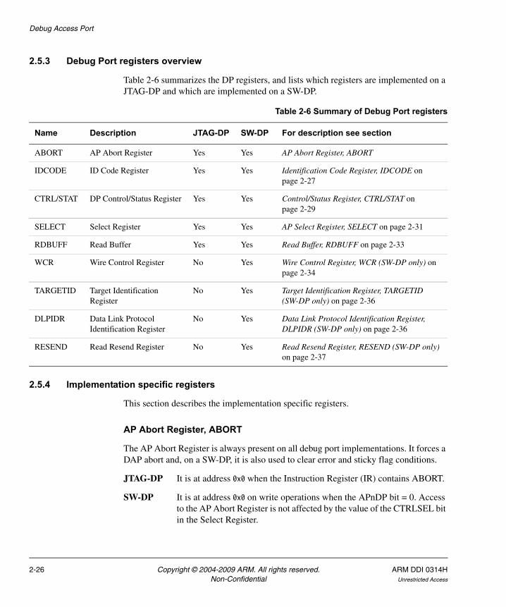
Debug Access Port
2.5.3 Debug Port registers overview
Table 2-6 summarizes the DP registers, and lists which registers are implemented on a JTAG-DP and which are implemented on a SW-DP.
2.5.4 Implementation specific registers
This section describes the implementation specific registers.
AP Abort Register, ABORT
The AP Abort Register is always present on all debug port implementations. It forces a DAP abort and, on a SW-DP, it is also used to clear error and sticky flag conditions.
JTAG-DP It is at address 0x0 when the Instruction Register (IR) contains ABORT.
SW-DP It is at address 0x0 on write operations when the APnDP bit = 0. Access to the AP Abort Register is not affected by the value of the CTRLSEL bit in the Select Register.
Table 2-6 Summary of Debug Port registers
Name Description JTAG-DP SW-DP For description see section
ABORT AP Abort Register Yes Yes AP Abort Register, ABORT
IDCODE ID Code Register Yes Yes Identification Code Register, IDCODE on page 2-27
CTRL/STAT DP Control/Status Register Yes Yes Control/Status Register, CTRL/STAT on page 2-29
SELECT Select Register Yes Yes AP Select Register, SELECT on page 2-31
RDBUFF Read Buffer Yes Yes Read Buffer, RDBUFF on page 2-33
WCR Wire Control Register No Yes Wire Control Register, WCR (SW-DP only) on page 2-34
TARGETID Target Identification Register
No Yes Target Identification Register, TARGETID (SW-DP only) on page 2-36
DLPIDR Data Link Protocol Identification Register
No Yes Data Link Protocol Identification Register, DLPIDR (SW-DP only) on page 2-36
RESEND Read Resend Register No Yes Read Resend Register, RESEND (SW-DP only) on page 2-37
2-26 Copyright © 2004-2009 ARM. All rights reserved. ARM DDI 0314HNon-Confidential Unrestricted Access
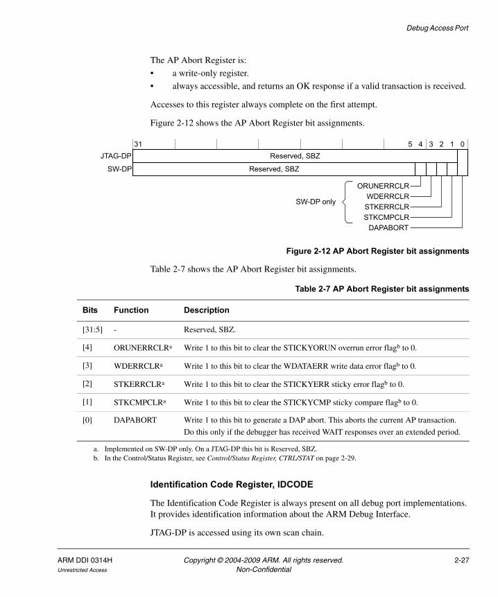
Debug Access Port
The AP Abort Register is:
• a write-only register.
• always accessible, and returns an OK response if a valid transaction is received.
Accesses to this register always complete on the first attempt.
Figure 2-12 shows the AP Abort Register bit assignments.
Figure 2-12 AP Abort Register bit assignments
Table 2-7 shows the AP Abort Register bit assignments.
Identification Code Register, IDCODE
The Identification Code Register is always present on all debug port implementations. It provides identification information about the ARM Debug Interface.
JTAG-DP is accessed using its own scan chain.
31 5 4 3 2 1 0Reserved, SBZ
Reserved, SBZ
JTAG-DP
SW-DP
ORUNERRCLRWDERRCLR
STKERRCLRSTKCMPCLR
DAPABORT
SW-DP only
Table 2-7 AP Abort Register bit assignments
Bits Function Description
[31:5] - Reserved, SBZ.
[4] ORUNERRCLRa Write 1 to this bit to clear the STICKYORUN overrun error flagb to 0.
[3] WDERRCLRa Write 1 to this bit to clear the WDATAERR write data error flagb to 0.
[2] STKERRCLRa Write 1 to this bit to clear the STICKYERR sticky error flagb to 0.
[1] STKCMPCLRa Write 1 to this bit to clear the STICKYCMP sticky compare flagb to 0.
[0] DAPABORT Write 1 to this bit to generate a DAP abort. This aborts the current AP transaction.
Do this only if the debugger has received WAIT responses over an extended period.
a. Implemented on SW-DP only. On a JTAG-DP this bit is Reserved, SBZ.b. In the Control/Status Register, see Control/Status Register, CTRL/STAT on page 2-29.
ARM DDI 0314H Copyright © 2004-2009 ARM. All rights reserved. 2-27Unrestricted Access Non-Confidential
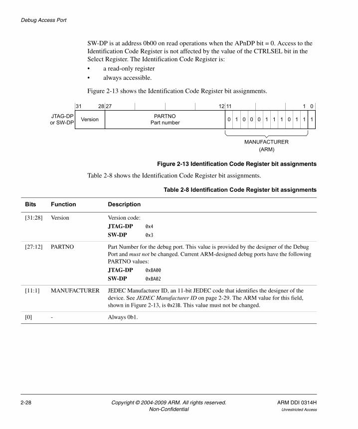
Debug Access Port
SW-DP is at address 0b00 on read operations when the APnDP bit = 0. Access to the Identification Code Register is not affected by the value of the CTRLSEL bit in the Select Register. The Identification Code Register is:
• a read-only register
• always accessible.
Figure 2-13 shows the Identification Code Register bit assignments.
Figure 2-13 Identification Code Register bit assignments
Table 2-8 shows the Identification Code Register bit assignments.
1Version
31 28 27 12 11 1 0
PARTNOPart number 0 1 0 0 0 1 1 1 0 1 1JTAG-DP
or SW-DP
MANUFACTURER(ARM)
Table 2-8 Identification Code Register bit assignments
Bits Function Description
[31:28] Version Version code:
JTAG-DP 0x4
SW-DP 0x3
[27:12] PARTNO Part Number for the debug port. This value is provided by the designer of the Debug Port and must not be changed. Current ARM-designed debug ports have the following PARTNO values:
JTAG-DP 0xBA00
SW-DP 0xBA02
[11:1] MANUFACTURER JEDEC Manufacturer ID, an 11-bit JEDEC code that identifies the designer of the device. See JEDEC Manufacturer ID on page 2-29. The ARM value for this field, shown in Figure 2-13, is 0x23B. This value must not be changed.
[0] - Always 0b1.
2-28 Copyright © 2004-2009 ARM. All rights reserved. ARM DDI 0314HNon-Confidential Unrestricted Access
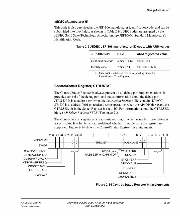
Debug Access Port
JEDEC Manufacturer ID
This code is also described as the JEP-106 manufacturer identification code, and can be subdivided into two fields, as shown in Table 2-9. JDEC codes are assigned by the JEDEC Solid State Technology Association, see JEP106M, Standard Manufacture's Identification Code.
Control/Status Register, CTRL/STAT
The Control/Status Register is always present on all debug port implementations. It provides control of the debug port, and status information about the debug port. JTAG-DP It is at address 0x4 when the Instruction Register (IR) contains DPACC. SW-DP is at address 0b01 on read and write operations when the APnDP bit = 0 and the CTRLSEL bit in the Select Register is set to b0. For information about the CTRLSEL bit see AP Select Register, SELECT on page 2-31.
The Control/Status Register is a read-write register, in which some bits have different access rights. It is Implementation-defined whether some fields in the register are supported. Figure 2-14 shows the Control/Status Register bit assignments.
Figure 2-14 Control/Status Register bit assignments
Table 2-9 JEDEC JEP-106 manufacturer ID code, with ARM values
JEP-106 field Bitsa
a. Field width, in bits, and the corresponding bits in the Identification Code Register.
ARM registered value
Continuation code 4 bits, [11:8] b0100, 0x4
Identity code 7 bits, [7:1] b0111011, 0x3B
0000
31 5 4 3 2 1 0
DAPSM-DP
SW-DP
WDATAERRREADOK
STICKYERR
TRNMODE
SW-DP only,RAZ/SBZP for DAPSM-DP
30 29 28 27 26 25 24 23 12 11 8 7 6
TRNCNT
CSYSPWRUPACKCSYSPWRUPREQCDBGPWRUPACKCDBGPWRUPREQ
CDBGRSTACKCDBGRSTREQ
RAZ/SBZP
MASKLANE
STICKYCMP
STICKYORUNORUNDETECT
ARM DDI 0314H Copyright © 2004-2009 ARM. All rights reserved. 2-29Unrestricted Access Non-Confidential
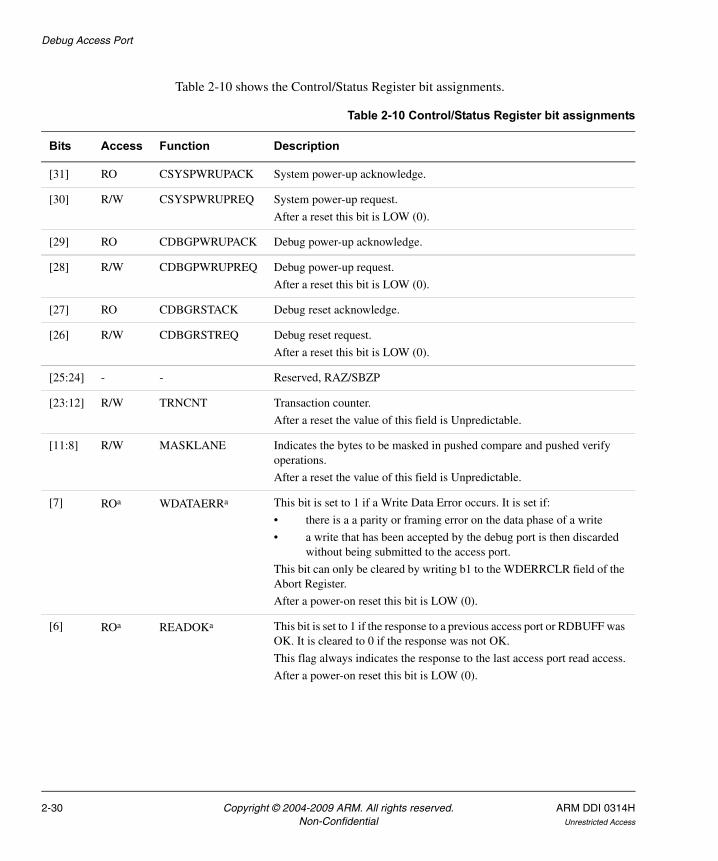
Debug Access Port
Table 2-10 shows the Control/Status Register bit assignments.
Table 2-10 Control/Status Register bit assignments
Bits Access Function Description
[31] RO CSYSPWRUPACK System power-up acknowledge.
[30] R/W CSYSPWRUPREQ System power-up request.
After a reset this bit is LOW (0).
[29] RO CDBGPWRUPACK Debug power-up acknowledge.
[28] R/W CDBGPWRUPREQ Debug power-up request.
After a reset this bit is LOW (0).
[27] RO CDBGRSTACK Debug reset acknowledge.
[26] R/W CDBGRSTREQ Debug reset request.
After a reset this bit is LOW (0).
[25:24] - - Reserved, RAZ/SBZP
[23:12] R/W TRNCNT Transaction counter.
After a reset the value of this field is Unpredictable.
[11:8] R/W MASKLANE Indicates the bytes to be masked in pushed compare and pushed verify operations.
After a reset the value of this field is Unpredictable.
[7] ROa WDATAERRa This bit is set to 1 if a Write Data Error occurs. It is set if:
• there is a a parity or framing error on the data phase of a write
• a write that has been accepted by the debug port is then discarded without being submitted to the access port.
This bit can only be cleared by writing b1 to the WDERRCLR field of the Abort Register.
After a power-on reset this bit is LOW (0).
[6] ROa READOKa This bit is set to 1 if the response to a previous access port or RDBUFF was OK. It is cleared to 0 if the response was not OK.
This flag always indicates the response to the last access port read access.
After a power-on reset this bit is LOW (0).
2-30 Copyright © 2004-2009 ARM. All rights reserved. ARM DDI 0314HNon-Confidential Unrestricted Access
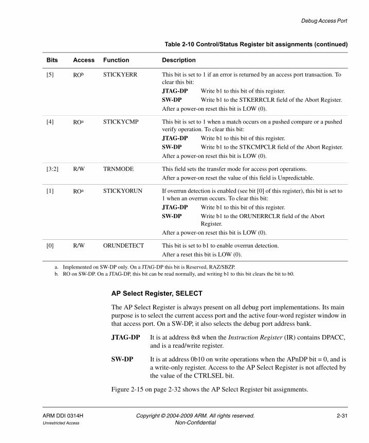
Debug Access Port
AP Select Register, SELECT
The AP Select Register is always present on all debug port implementations. Its main purpose is to select the current access port and the active four-word register window in that access port. On a SW-DP, it also selects the debug port address bank.
JTAG-DP It is at address 0x8 when the Instruction Register (IR) contains DPACC, and is a read/write register.
SW-DP It is at address 0b10 on write operations when the APnDP bit = 0, and is a write-only register. Access to the AP Select Register is not affected by the value of the CTRLSEL bit.
Figure 2-15 on page 2-32 shows the AP Select Register bit assignments.
[5] ROb STICKYERR This bit is set to 1 if an error is returned by an access port transaction. To clear this bit:
JTAG-DP Write b1 to this bit of this register.
SW-DP Write b1 to the STKERRCLR field of the Abort Register.
After a power-on reset this bit is LOW (0).
[4] ROa STICKYCMP This bit is set to 1 when a match occurs on a pushed compare or a pushed verify operation. To clear this bit:
JTAG-DP Write b1 to this bit of this register.
SW-DP Write b1 to the STKCMPCLR field of the Abort Register.
After a power-on reset this bit is LOW (0).
[3:2] R/W TRNMODE This field sets the transfer mode for access port operations.
After a power-on reset the value of this field is Unpredictable.
[1] ROa STICKYORUN If overrun detection is enabled (see bit [0] of this register), this bit is set to 1 when an overrun occurs. To clear this bit:
JTAG-DP Write b1 to this bit of this register.
SW-DP Write b1 to the ORUNERRCLR field of the Abort Register.
After a power-on reset this bit is LOW (0).
[0] R/W ORUNDETECT This bit is set to b1 to enable overrun detection.
After a reset this bit is LOW (0).
a. Implemented on SW-DP only. On a JTAG-DP this bit is Reserved, RAZ/SBZP.b. RO on SW-DP. On a JTAG-DP, this bit can be read normally, and writing b1 to this bit clears the bit to b0.
Table 2-10 Control/Status Register bit assignments (continued)
Bits Access Function Description
ARM DDI 0314H Copyright © 2004-2009 ARM. All rights reserved. 2-31Unrestricted Access Non-Confidential
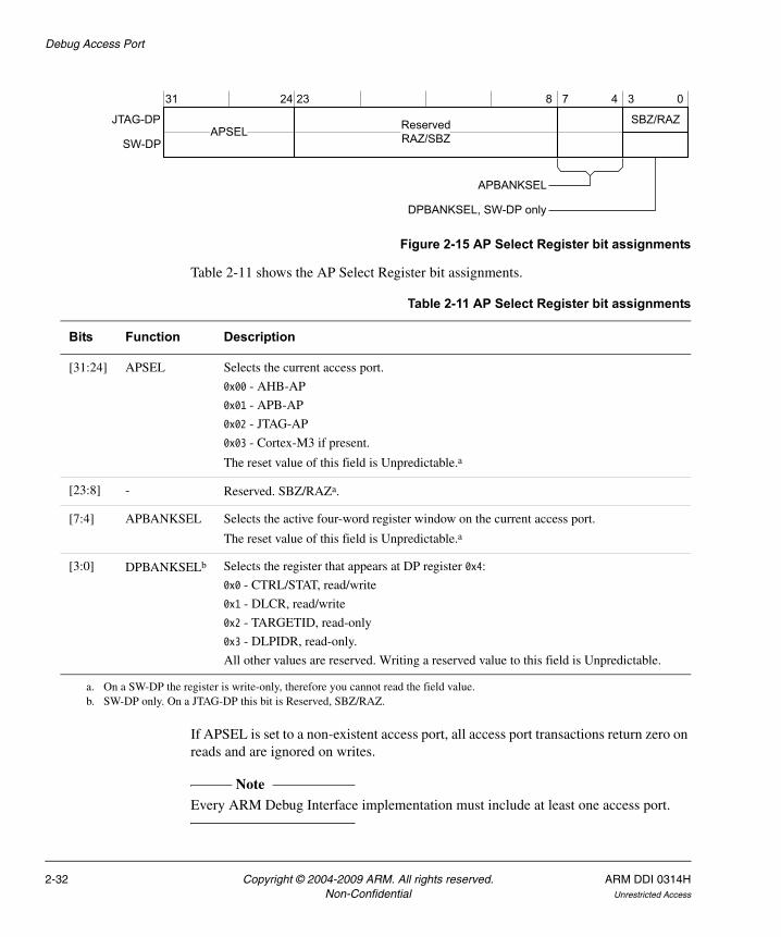
Debug Access Port
Figure 2-15 AP Select Register bit assignments
Table 2-11 shows the AP Select Register bit assignments.
If APSEL is set to a non-existent access port, all access port transactions return zero on reads and are ignored on writes.
Note Every ARM Debug Interface implementation must include at least one access port.
SBZ/RAZAPSEL
31 4 3 0
JTAG-DP
SW-DP
APBANKSEL
DPBANKSEL, SW-DP only
24 23 8 7
ReservedRAZ/SBZ
Table 2-11 AP Select Register bit assignments
Bits Function Description
[31:24] APSEL Selects the current access port.
0x00 - AHB-AP
0x01 - APB-AP
0x02 - JTAG-AP
0x03 - Cortex-M3 if present.
The reset value of this field is Unpredictable.a
[23:8] - Reserved. SBZ/RAZa.
[7:4] APBANKSEL Selects the active four-word register window on the current access port.
The reset value of this field is Unpredictable.a
[3:0] DPBANKSELb Selects the register that appears at DP register 0x4:
0x0 - CTRL/STAT, read/write
0x1 - DLCR, read/write
0x2 - TARGETID, read-only
0x3 - DLPIDR, read-only.
All other values are reserved. Writing a reserved value to this field is Unpredictable.
a. On a SW-DP the register is write-only, therefore you cannot read the field value.b. SW-DP only. On a JTAG-DP this bit is Reserved, SBZ/RAZ.
2-32 Copyright © 2004-2009 ARM. All rights reserved. ARM DDI 0314HNon-Confidential Unrestricted Access
Debug Access Port
Read Buffer, RDBUFF
The 32-bit Read Buffer is always present on all debug port implementations. However, there are significant differences in its implementation on JTAG and SW Debug Ports.
JTAG-DP It is at address 0xC when the Instruction Register (IR) contains DPACC, and is a Read-as-zero, Writes ignored (RAZ/WI) register.
SW-DP It is at address 0b11 on read operations when the APnDP bit = 0 and is a read-only register. Access to the Read Buffer is not affected by the value of the CTRLSEL bit in the SELECT Register.
Read Buffer implementation and use on a JTAG-DP
On a JTAG-DP, the Read Buffer always reads as zero, and writes to the Read Buffer address are ignored.
The Read Buffer is architecturally defined to provide a debug port read operation that does not have any side effects. This means that a debugger can insert a debug port read of the Read Buffer at the end of a sequence of operations, to return the final Read Result and ACK values.
Read Buffer implementation and use on a SW-DP
On a SW-DP, performing a read of the Read Buffer captures data from the access port, presented as the result of a previous read, without initiating a new access port transaction. This means that reading the Read Buffer returns the result of the last access port read access, without generating a new AP access.
After you have read the Read Buffer, its contents are no longer valid. The result of a second read of the Read Buffer is Unpredictable.
If you require the value from an access port register read, that read must be followed by one of:
• A second access port register read. You can read the Control/Status Register (CSW) if you want to ensure that this second read has no side effects.
• A read of the DP Read Buffer.
This second access, to the access port or the debug port depending on which option you used, stalls until the result of the original access port read is available.
ARM DDI 0314H Copyright © 2004-2009 ARM. All rights reserved. 2-33Unrestricted Access Non-Confidential
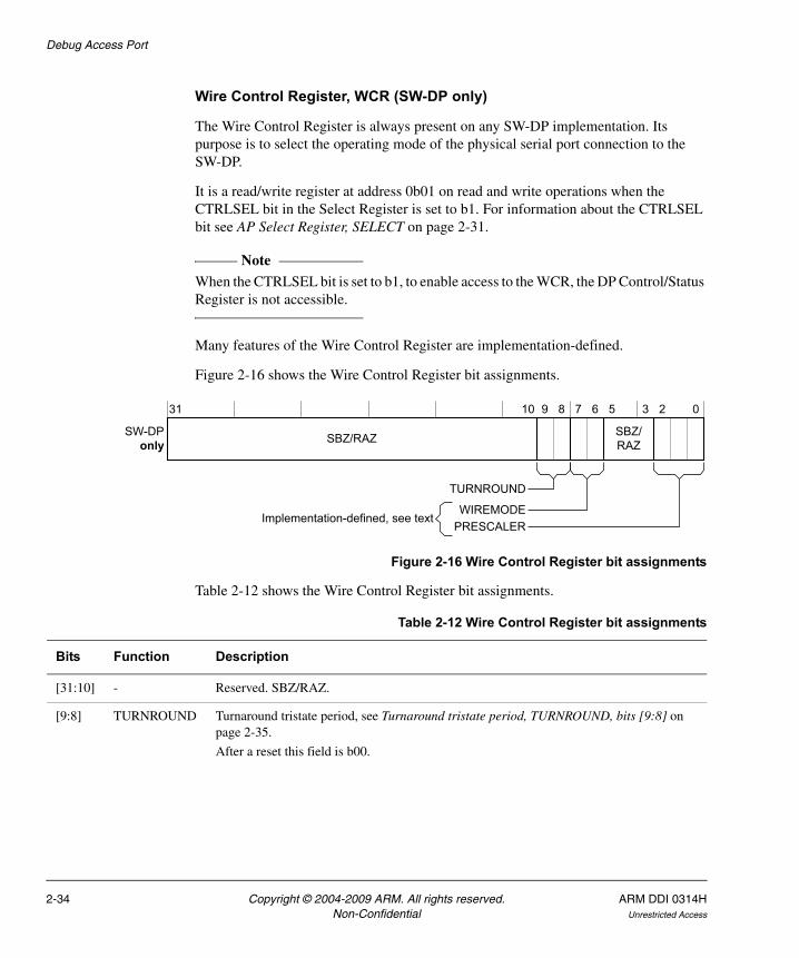
Debug Access Port
Wire Control Register, WCR (SW-DP only)
The Wire Control Register is always present on any SW-DP implementation. Its purpose is to select the operating mode of the physical serial port connection to the SW-DP.
It is a read/write register at address 0b01 on read and write operations when the CTRLSEL bit in the Select Register is set to b1. For information about the CTRLSEL bit see AP Select Register, SELECT on page 2-31.
Note When the CTRLSEL bit is set to b1, to enable access to the WCR, the DP Control/Status Register is not accessible.
Many features of the Wire Control Register are implementation-defined.
Figure 2-16 shows the Wire Control Register bit assignments.
Figure 2-16 Wire Control Register bit assignments
Table 2-12 shows the Wire Control Register bit assignments.
SBZ/RAZSBZ/RAZ
31 0
SW-DPonly
10 9 8 7 6 5 3 2
TURNROUND
WIREMODEPRESCALER
Implementation-defined, see text
Table 2-12 Wire Control Register bit assignments
Bits Function Description
[31:10] - Reserved. SBZ/RAZ.
[9:8] TURNROUND Turnaround tristate period, see Turnaround tristate period, TURNROUND, bits [9:8] on page 2-35.
After a reset this field is b00.
2-34 Copyright © 2004-2009 ARM. All rights reserved. ARM DDI 0314HNon-Confidential Unrestricted Access
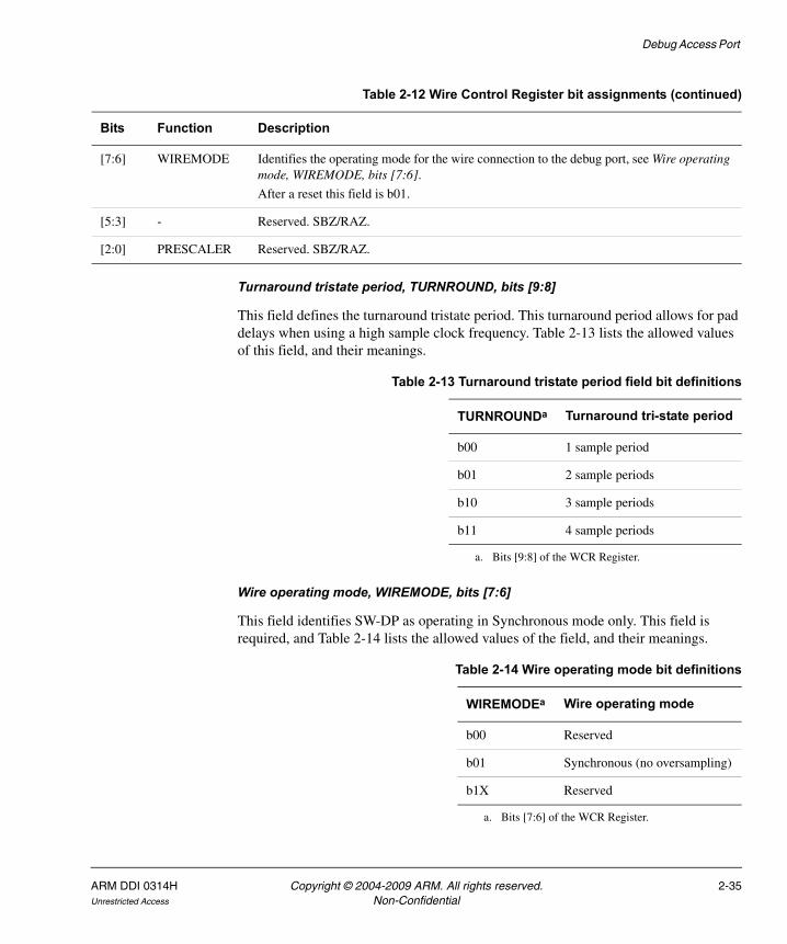
Debug Access Port
Turnaround tristate period, TURNROUND, bits [9:8]
This field defines the turnaround tristate period. This turnaround period allows for pad delays when using a high sample clock frequency. Table 2-13 lists the allowed values of this field, and their meanings.
Wire operating mode, WIREMODE, bits [7:6]
This field identifies SW-DP as operating in Synchronous mode only. This field is required, and Table 2-14 lists the allowed values of the field, and their meanings.
[7:6] WIREMODE Identifies the operating mode for the wire connection to the debug port, see Wire operating mode, WIREMODE, bits [7:6].
After a reset this field is b01.
[5:3] - Reserved. SBZ/RAZ.
[2:0] PRESCALER Reserved. SBZ/RAZ.
Table 2-12 Wire Control Register bit assignments (continued)
Bits Function Description
Table 2-13 Turnaround tristate period field bit definitions
TURNROUNDa
a. Bits [9:8] of the WCR Register.
Turnaround tri-state period
b00 1 sample period
b01 2 sample periods
b10 3 sample periods
b11 4 sample periods
Table 2-14 Wire operating mode bit definitions
WIREMODEa
a. Bits [7:6] of the WCR Register.
Wire operating mode
b00 Reserved
b01 Synchronous (no oversampling)
b1X Reserved
ARM DDI 0314H Copyright © 2004-2009 ARM. All rights reserved. 2-35Unrestricted Access Non-Confidential

Debug Access Port
Target Identification Register, TARGETID (SW-DP only)
The Target Identification Register provides information about the target when the host is connected to a single device. The Target Identification Register is:
• a read-only register
• accessed by a read of DP register 0x4 when the DPBANKSEL bit in the SELECT Register is set to 0x2.
The value of this register reflects the value of the TARGETID[31:0] input.
Figure 2-17 shows the Target Identification Register bit assignments.
Figure 2-17 Target Identification Register bit assignments
Table 2-15 shows the Target Identification Register bit assignments.
Data Link Protocol Identification Register, DLPIDR (SW-DP only)
The Data Link Protocol Identification Register provides information about the Serial Wire protocol version. The Data Link Protocol Identification Register is:
• a read-only register
• accessed by a read of DP register 0x4 when the DPBANKSEL bit in the SELECT Register is set to 0x3.
31 28 27 12 11 1 0
TPARTNO TDESIGNER
TREVISION Reserved, RAO
Table 2-15 Target Identification Register bit assignments
Bits Function Description
[31:28] TREVISION Target revision.
[27:12] TPARTNO Implementation defined. This value is assigned by the designer of the part and must be unique to that part.
[11:1] TDESIGNER Implementation defined. This field identifies the designer of the part. The value is based on the code assigned to the designer by JEDEC standard JEP-106, as used in IEEE 1149.1.
[0] - Reserved, RAO.
2-36 Copyright © 2004-2009 ARM. All rights reserved. ARM DDI 0314HNon-Confidential Unrestricted Access
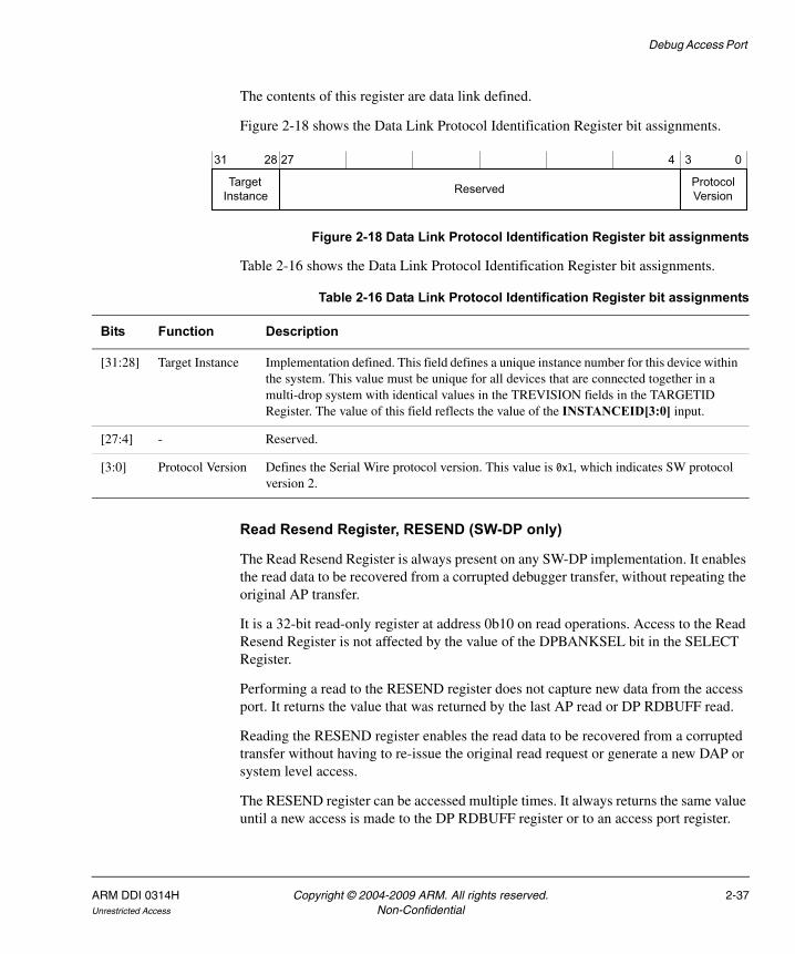
Debug Access Port
The contents of this register are data link defined.
Figure 2-18 shows the Data Link Protocol Identification Register bit assignments.
Figure 2-18 Data Link Protocol Identification Register bit assignments
Table 2-16 shows the Data Link Protocol Identification Register bit assignments.
Read Resend Register, RESEND (SW-DP only)
The Read Resend Register is always present on any SW-DP implementation. It enables the read data to be recovered from a corrupted debugger transfer, without repeating the original AP transfer.
It is a 32-bit read-only register at address 0b10 on read operations. Access to the Read Resend Register is not affected by the value of the DPBANKSEL bit in the SELECT Register.
Performing a read to the RESEND register does not capture new data from the access port. It returns the value that was returned by the last AP read or DP RDBUFF read.
Reading the RESEND register enables the read data to be recovered from a corrupted transfer without having to re-issue the original read request or generate a new DAP or system level access.
The RESEND register can be accessed multiple times. It always returns the same value until a new access is made to the DP RDBUFF register or to an access port register.
Protocol Version
Target Instance
31 28 27 4 3 0
Reserved
Table 2-16 Data Link Protocol Identification Register bit assignments
Bits Function Description
[31:28] Target Instance Implementation defined. This field defines a unique instance number for this device within the system. This value must be unique for all devices that are connected together in a multi-drop system with identical values in the TREVISION fields in the TARGETID Register. The value of this field reflects the value of the INSTANCEID[3:0] input.
[27:4] - Reserved.
[3:0] Protocol Version Defines the Serial Wire protocol version. This value is 0x1, which indicates SW protocol version 2.
ARM DDI 0314H Copyright © 2004-2009 ARM. All rights reserved. 2-37Unrestricted Access Non-Confidential
Debug Access Port
2.6 Access portsAn access port provides the interface between the debug port interface and one or more debug components present within the system. There are two kinds of access port supplied with this DAP:
• Memory Access Ports (MEM-AP), which are designed for connection to memory bus system with address and data controls.
• JTAG Access Ports (JTAG-AP) for connecting to on-chip based debug TAPs.
All access ports follow a base standard for identification, and debuggers must be able to recognize and ignore access ports that they do not support. The connection method does not depend on the type of debug port used and the type of access port being accessed.
For more information on access ports and recommend debugger interaction with access ports, see the ARM Debug Interface v5 Architecture Specification and the ARM Debug Interface v5.1 Architecture Supplement.
2.6.1 Overview
There are three access ports supplied in the DAP, and it is possible to connect a fourth access port externally. The supplied access ports within this release are:
• AHB-AP for connection to the main system bus
• APB-AP to enable direct connection to the dedicated Debug Bus
• JTAG-AP to control up to eight scan chains.
Another connection, to a fourth access port, is exported from the DAP. This is described in Auxiliary Access Port on page 2-65.
2-38 Copyright © 2004-2009 ARM. All rights reserved. ARM DDI 0314HNon-Confidential Unrestricted Access
Debug Access Port
2.7 AHB-APThe AHB-AP implements the MEM-AP architecture to directly connect to an AHB based memory system. Connection to other memory systems is possible through suitable bridging local.
As part of the MEM-AP description, the AHB-AP has a number of implementation specific features described in:
• External interfaces
• Implementation features on page 2-42
• Programmers model overview on page 2-43
• DAP transfers on page 2-47
• Differentiation between system and access port initiated error responses on page 2-49
• Effects of resets on page 2-49
• Effects of power down signals on page 2-49
• AHB-AP dual power domain support on page 2-50.
For information about all the registers and features in a MEM-AP, see the ARM Debug Interface v5 Architecture Specification and the ARM Debug Interface v5.1 Architecture Supplement.
2.7.1 External interfaces
The primary external interface to the system is an AHB-Lite master port supporting the following:
• AHB in AMBA v2.0
• ARM11 AMBA extensions
• TrustZone extensions.
The AHB-Lite master port does not support the following:
• BURST and SEQ
• Exclusive accesses
• Unaligned transfers.
ARM DDI 0314H Copyright © 2004-2009 ARM. All rights reserved. 2-39Unrestricted Access Non-Confidential
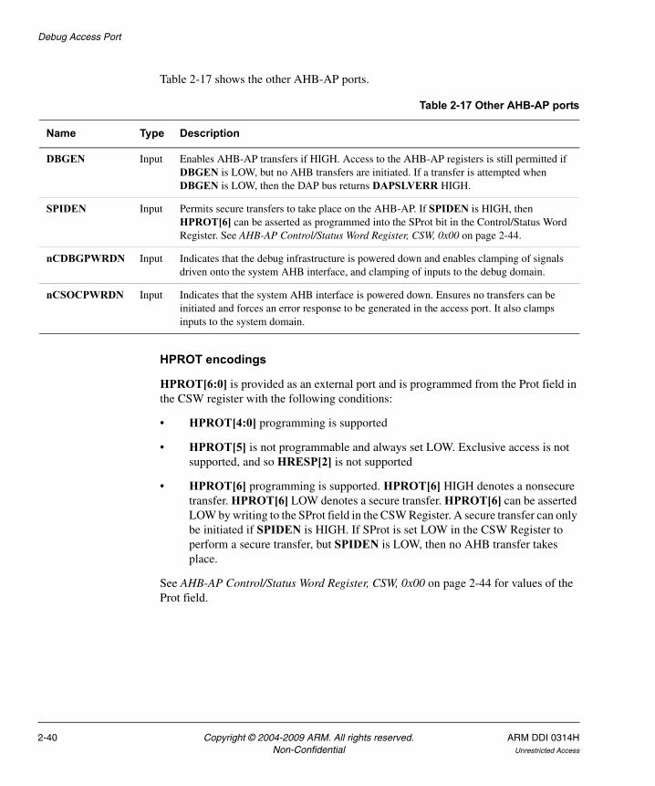
Debug Access Port
Table 2-17 shows the other AHB-AP ports.
HPROT encodings
HPROT[6:0] is provided as an external port and is programmed from the Prot field in the CSW register with the following conditions:
• HPROT[4:0] programming is supported
• HPROT[5] is not programmable and always set LOW. Exclusive access is not supported, and so HRESP[2] is not supported
• HPROT[6] programming is supported. HPROT[6] HIGH denotes a nonsecure transfer. HPROT[6] LOW denotes a secure transfer. HPROT[6] can be asserted LOW by writing to the SProt field in the CSW Register. A secure transfer can only be initiated if SPIDEN is HIGH. If SProt is set LOW in the CSW Register to perform a secure transfer, but SPIDEN is LOW, then no AHB transfer takes place.
See AHB-AP Control/Status Word Register, CSW, 0x00 on page 2-44 for values of the Prot field.
Table 2-17 Other AHB-AP ports
Name Type Description
DBGEN Input Enables AHB-AP transfers if HIGH. Access to the AHB-AP registers is still permitted if DBGEN is LOW, but no AHB transfers are initiated. If a transfer is attempted when DBGEN is LOW, then the DAP bus returns DAPSLVERR HIGH.
SPIDEN Input Permits secure transfers to take place on the AHB-AP. If SPIDEN is HIGH, then HPROT[6] can be asserted as programmed into the SProt bit in the Control/Status Word Register. See AHB-AP Control/Status Word Register, CSW, 0x00 on page 2-44.
nCDBGPWRDN Input Indicates that the debug infrastructure is powered down and enables clamping of signals driven onto the system AHB interface, and clamping of inputs to the debug domain.
nCSOCPWRDN Input Indicates that the system AHB interface is powered down. Ensures no transfers can be initiated and forces an error response to be generated in the access port. It also clamps inputs to the system domain.
2-40 Copyright © 2004-2009 ARM. All rights reserved. ARM DDI 0314HNon-Confidential Unrestricted Access
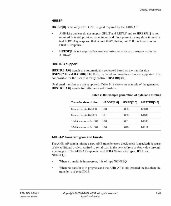
Debug Access Port
HRESP
HRESP[0] is the only RESPONSE signal required by the AHB-AP:
• AHB-Lite devices do not support SPLIT and RETRY and so HRESP[1] is not required. It is still provided as an input, and if not present on any slave it must be tied LOW. Any response that is not OKAY, that is, not 2'b00, is treated as an ERROR response.
• HRESP[2] is not required because exclusive accesses are unsupported in the AHB-AP.
HBSTRB support
HBSTRB[3:0] signals are automatically generated based on the transfer size HSIZE[2:0] and HADDR[1:0]. Byte, halfword and word transfers are supported. It is not possible for the user to directly control HBSTRB[3:0].
Unaligned transfers are not supported. Table 2-18 shows an example of the generated HBSTRB[3:0] signals for different-sized transfers.
AHB-AP transfer types and bursts
The AHB-AP cannot initiate a new AHB transfer every clock cycle (unpacked) because of the additional cycles required to serial scan in the new address or data value through a debug port. The AHB-AP supports two HTRANS transfer types, IDLE and NONSEQ:
• When a transfer is in progress, it is of type NONSEQ
• When no transfer is in progress and the AHB-AP is still granted the bus then the transfer is of type IDLE.
Table 2-18 Example generation of byte lane strobes
Transfer description HADDR[1:0] HSIZE[2:0] HBSTRB[3:0]
8-bit access to 0x1000 b00 b000 b0001
8-bit access to 0x1003 b11 b000 b1000
16-bit access to 0x1002 b10 b001 b1100
32-bit access to 0x1004 b00 b010 b1111
ARM DDI 0314H Copyright © 2004-2009 ARM. All rights reserved. 2-41Unrestricted Access Non-Confidential
Debug Access Port
The only unpacked HBURST encoding supported is SINGLE. Packed 8-bit transfers or 16-bit transfers are treated as individual NONSEQ, SINGLE transfers at the AHB-Lite interface. This ensures that there are no issues with boundary wrapping, to avoid additional AHB-AP complexity.
A full AHB master interface can be created by adding an AHB-Lite to AHB wrapper to the output of the AHB-AP, as provided in the AMBA Design Kit.
2.7.2 Implementation features
The AHB-AP provides the following specific MEM-AP features:
• Auto-incrementing of the Transfer Address Register with address wrapping on 1k byte boundaries
• Word, half-word and byte accesses to devices present on the AHB memory system
• Packed transfers on sub-word transfers
The AHB-AP does not support the following MEM-AP features:
• Big endian. All accesses performed as expected to be to a little endian memory structure
• Slave memory port disabling. The AHB-Lite master interface is not shared with any other connection so there is no slave port to disable access to this interface. If the memory map presented to the AHB-AP is to be shared with another AHB-Lite master then this is implemented externally to the DAP.
The AHB-AP has two clock domains:
• DAPCLK Drives the DAP bus interface and access control for register read and writes. DAPCLK must be driven by a constant clock. When started, it must not be stopped or altered while the DAP is in use.
• HCLK AHB clock domain driving AHB interface. DAPCLK and HCLK are asynchronous domains. Synchronizers are used between the Access Control block and the AHB master interface.
DAPRESETn initializes the state of all registers in the DAPCLK domain. DAPRESETn enables initialization of the DAP without affecting the normal operation of the SoC in which the DAP is integrated, and must be driven by the tools on external connection by accessing the appropriate location in the debug port. HRESETn is used to reset the AHB interface and does not reset any state in the DAP interface
2-42 Copyright © 2004-2009 ARM. All rights reserved. ARM DDI 0314HNon-Confidential Unrestricted Access
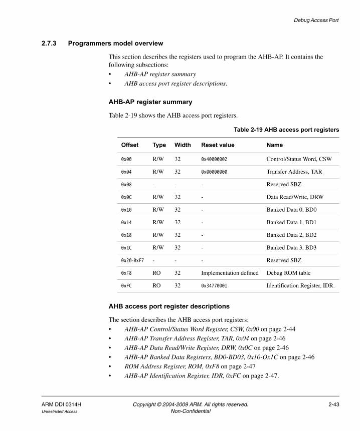
Debug Access Port
2.7.3 Programmers model overview
This section describes the registers used to program the AHB-AP. It contains the following subsections:
• AHB-AP register summary
• AHB access port register descriptions.
AHB-AP register summary
Table 2-19 shows the AHB access port registers.
AHB access port register descriptions
The section describes the AHB access port registers:
• AHB-AP Control/Status Word Register, CSW, 0x00 on page 2-44
• AHB-AP Transfer Address Register, TAR, 0x04 on page 2-46
• AHB-AP Data Read/Write Register, DRW, 0x0C on page 2-46
• AHB-AP Banked Data Registers, BD0-BD03, 0x10-Ox1C on page 2-46
• ROM Address Register, ROM, 0xF8 on page 2-47
• AHB-AP Identification Register, IDR, 0xFC on page 2-47.
Table 2-19 AHB access port registers
Offset Type Width Reset value Name
0x00 R/W 32 0x40000002 Control/Status Word, CSW
0x04 R/W 32 0x00000000 Transfer Address, TAR
0x08 - - - Reserved SBZ
0x0C R/W 32 - Data Read/Write, DRW
0x10 R/W 32 - Banked Data 0, BD0
0x14 R/W 32 - Banked Data 1, BD1
0x18 R/W 32 - Banked Data 2, BD2
0x1C R/W 32 - Banked Data 3, BD3
0x20-0xF7 - - - Reserved SBZ
0xF8 RO 32 Implementation defined Debug ROM table
0xFC RO 32 0x34770001 Identification Register, IDR.
ARM DDI 0314H Copyright © 2004-2009 ARM. All rights reserved. 2-43Unrestricted Access Non-Confidential
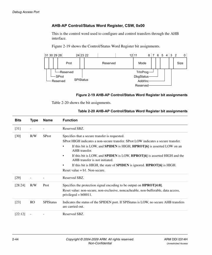
Debug Access Port
AHB-AP Control/Status Word Register, CSW, 0x00
This is the control word used to configure and control transfers through the AHB interface.
Figure 2-19 shows the Control/Status Word Register bit assignments.
Figure 2-19 AHB-AP Control/Status Word Register bit assignments
Table 2-20 shows the bit assignments.
Size
31 30 29 28 24 23 12 11 8 7 6 5 4 3 2 0
Prot Reserved Mode
TrInProgDbgStatus
AddrIncReserved
ReservedSProt
Reserved SPIStatus
22
Table 2-20 AHB-AP Control/Status Word Register bit assignments
Bits Type Name Function
[31] - - Reserved SBZ.
[30] R/W SProt Specifies that a secure transfer is requested.
SProt HIGH indicates a non-secure transfer. SProt LOW indicates a secure transfer.
• If this bit is LOW, and SPIDEN is HIGH, HPROT[6] is asserted LOW on an AHB transfer.
• If this bit is LOW, and SPIDEN is LOW, HPROT[6] is asserted HIGH and the AHB transfer is not initiated.
• If this bit is HIGH, the state of SPIDEN is ignored. HPROT[6] is HIGH.
Reset value = b1. Non-secure.
[29] - - Reserved SBZ.
[28:24] R/W Prot Specifies the protection signal encoding to be output on HPROT[4:0].Reset value: non-secure, non-exclusive, noncacheable, non-bufferable, data access, privileged = b00011.
[23] RO SPIStatus Indicates the status of the SPIDEN port. If SPIStatus is LOW, no secure AHB transfers are carried out.
[22:12] - - Reserved SBZ.
2-44 Copyright © 2004-2009 ARM. All rights reserved. ARM DDI 0314HNon-Confidential Unrestricted Access
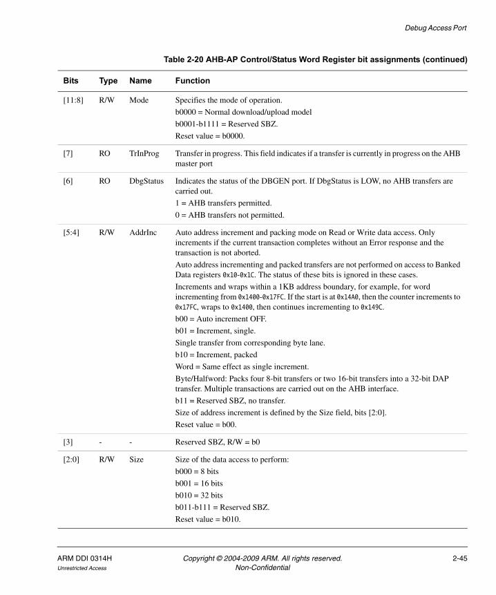
Debug Access Port
[11:8] R/W Mode Specifies the mode of operation.
b0000 = Normal download/upload model
b0001-b1111 = Reserved SBZ.
Reset value = b0000.
[7] RO TrInProg Transfer in progress. This field indicates if a transfer is currently in progress on the AHB master port
[6] RO DbgStatus Indicates the status of the DBGEN port. If DbgStatus is LOW, no AHB transfers are carried out.
1 = AHB transfers permitted.
0 = AHB transfers not permitted.
[5:4] R/W AddrInc Auto address increment and packing mode on Read or Write data access. Only increments if the current transaction completes without an Error response and the transaction is not aborted.
Auto address incrementing and packed transfers are not performed on access to Banked Data registers 0x10-0x1C. The status of these bits is ignored in these cases.
Increments and wraps within a 1KB address boundary, for example, for word incrementing from 0x1400-0x17FC. If the start is at 0x14A0, then the counter increments to 0x17FC, wraps to 0x1400, then continues incrementing to 0x149C.
b00 = Auto increment OFF.
b01 = Increment, single.
Single transfer from corresponding byte lane.
b10 = Increment, packed
Word = Same effect as single increment.
Byte/Halfword: Packs four 8-bit transfers or two 16-bit transfers into a 32-bit DAP transfer. Multiple transactions are carried out on the AHB interface.
b11 = Reserved SBZ, no transfer.
Size of address increment is defined by the Size field, bits [2:0].
Reset value = b00.
[3] - - Reserved SBZ, R/W = b0
[2:0] R/W Size Size of the data access to perform:
b000 = 8 bits
b001 = 16 bits
b010 = 32 bits
b011-b111 = Reserved SBZ.
Reset value = b010.
Table 2-20 AHB-AP Control/Status Word Register bit assignments (continued)
Bits Type Name Function
ARM DDI 0314H Copyright © 2004-2009 ARM. All rights reserved. 2-45Unrestricted Access Non-Confidential
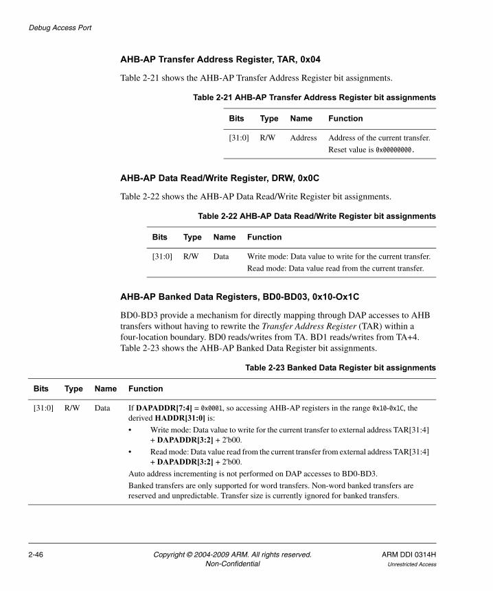
Debug Access Port
AHB-AP Transfer Address Register, TAR, 0x04
Table 2-21 shows the AHB-AP Transfer Address Register bit assignments.
AHB-AP Data Read/Write Register, DRW, 0x0C
Table 2-22 shows the AHB-AP Data Read/Write Register bit assignments.
AHB-AP Banked Data Registers, BD0-BD03, 0x10-Ox1C
BD0-BD3 provide a mechanism for directly mapping through DAP accesses to AHB transfers without having to rewrite the Transfer Address Register (TAR) within a four-location boundary. BD0 reads/writes from TA. BD1 reads/writes from TA+4. Table 2-23 shows the AHB-AP Banked Data Register bit assignments.
Table 2-21 AHB-AP Transfer Address Register bit assignments
Bits Type Name Function
[31:0] R/W Address Address of the current transfer.
Reset value is 0x00000000.
Table 2-22 AHB-AP Data Read/Write Register bit assignments
Bits Type Name Function
[31:0] R/W Data Write mode: Data value to write for the current transfer.
Read mode: Data value read from the current transfer.
Table 2-23 Banked Data Register bit assignments
Bits Type Name Function
[31:0] R/W Data If DAPADDR[7:4] = 0x0001, so accessing AHB-AP registers in the range 0x10-0x1C, the derived HADDR[31:0] is:
• Write mode: Data value to write for the current transfer to external address TAR[31:4] + DAPADDR[3:2] + 2'b00.
• Read mode: Data value read from the current transfer from external address TAR[31:4] + DAPADDR[3:2] + 2'b00.
Auto address incrementing is not performed on DAP accesses to BD0-BD3.
Banked transfers are only supported for word transfers. Non-word banked transfers are reserved and unpredictable. Transfer size is currently ignored for banked transfers.
2-46 Copyright © 2004-2009 ARM. All rights reserved. ARM DDI 0314HNon-Confidential Unrestricted Access
Debug Access Port
ROM Address Register, ROM, 0xF8
Table 2-24 shows the ROM Address Register bit assignments.
AHB-AP Identification Register, IDR, 0xFC
Figure 2-20 shows the AHB-AP Identification Register bit assignments.
Figure 2-20 AHB-AP Identification Register bit assignments
Table 2-25 shows the AHB-AP Identification Register bit assignments.
2.7.4 DAP transfers
This section describes:
• DAP transfer aborts on page 2-48
• Error response generation on page 2-48.
Table 2-24 ROM Address Register bit assignments
Bits Type Name Function
[31:0] RO Debug AHB ROM Address Base address of a ROM table. The ROM provides a look-up table for system components. Set to 0xFFFFFFFF in the AHB-AP in the initial release.
Revision
31 28 27 24 23 17 16 15 8 7 0
JEDEC bank JEDEC code Reserved Identity value
Mem AP
Table 2-25 AHB-AP Identification Register bit assignments
Bits Type Name Value Meaning
[31:28] RO Revision 0x4 Revision 4
[27:24] RO JEDEC bank 0x4 Designed by ARM
[23:17] RO JEDEC code 0x3B Designed by ARM
[16] RO Mem AP 0x1 Is a Mem AP
[15:8] - Reserved 0x00 -
[7:0] RO Identity value 0x01 AHB-AP
ARM DDI 0314H Copyright © 2004-2009 ARM. All rights reserved. 2-47Unrestricted Access Non-Confidential
Debug Access Port
DAP transfer aborts
The AHB-AP does not cancel the system-facing operation and returns DAPREADY HIGH one cycle after DAPABORT has been asserted by the driving debug port. The externally driving AHB master port does not violate the AHB protocol. After a transfer has been aborted, the Control/Status Word Register can be read to determine the state of the transfer in progress bit, TrInProg. When TrInProg returns to zero, either because the external transfer completes, or because of a reset, the AHB-AP returns to normal operation. All other writes to the AHB-AP are ignored until this bit is returned LOW after a Transfer Abort.
Error response generation
This section describes:
• System initiated error response
• Access port initiated error response
• AHB-AP reads after an abort
• AHB-AP writes after an abort.
System initiated error response
An error response received on the system driving master propagates onto the DAP bus when the transfer is completed. This response is received by the debug ports.
Access port initiated error response
Access port initiated error responses are:
• AHB-AP reads after an abort
• AHB-AP writes after an abort.
AHB-AP reads after an abort
After a DAPABORT operation has been carried out, and an external transfer is still pending, that is, the TrInProg bit is still HIGH, reads of all registers return a normal response except for reads of the Data Read/Write Register and banked registers which cannot initiate a new system read transfer. Reads of the Data Read/Write Register and banked registers return an error response until the TrInProg bit in the Control/Status Word Register is cleared because of the system transfer completing, or because of a reset.
AHB-AP writes after an abort
After a DAPABORT operation has been carried out, and an external transfer is still pending, that is, the transfer in progress bit is still HIGH, all writes to the access port return an error response, because they are ignored until the TrInProg bit is cleared.
2-48 Copyright © 2004-2009 ARM. All rights reserved. ARM DDI 0314HNon-Confidential Unrestricted Access
Debug Access Port
2.7.5 Differentiation between system and access port initiated error responses
If DAPSLVERR is HIGH and TrInProg is LOW in the Control/Status Word Register, the error is from either:
• a system error response if DBGEN and SPIDEN permit the transfer to be initiated
• an AHB-AP error response if DBGEN and SPIDEN do not permit the transfer to be initiated.
Table 2-26 shows the options.
If DAPSLVERR is HIGH and TrInProg is HIGH, then the error is from an access port error response. The transfer has not been accepted by the access port. This case can only occur after an abort has been initiated and the system transfer has not completed.
2.7.6 Effects of resets
The HRESETn signal can be asserted LOW at any time. The DAP interface must return DAPSLVERR for the current transaction.
The DAPRESETn signal must only be asserted LOW if there is no pending transaction on the AHB interface.
2.7.7 Effects of power down signals
The nCSOCPWRDN signal can be asserted LOW at any time. The DAP interface must return DAPSLVERR for the current transaction. The nCDBGPWRDN signal must only be asserted LOW if there is no pending transaction on the AHB interface.
Table 2-26 Error responses with DAPSLVERR HIGH and TrInProg LOW
SProt SPIDEN DBGEN Error response from Reason
x x 0 AHB-AP No transfers permitted
0 0 1 AHB-AP Secure transfers not permitted
0 1 1 System Secure transfer produced an error response
1 x 1 System Non secure transfer produced an error response
ARM DDI 0314H Copyright © 2004-2009 ARM. All rights reserved. 2-49Unrestricted Access Non-Confidential

Debug Access Port
2.7.8 AHB-AP dual power domain support
If the AHB-AP is split across multiple power domains, with the DAPCLK driven side in the Debug domain, and the AHB master port in the SoC power domain, clamping logic must be instantiated on the outputs of signals crossing each power-down domain. See the CoreSight Components Implementation Guide and the applicable Integration Manual for more information.
RTL hierarchy
Figure 2-21 shows the RTL structure to support power domain separation.
Figure 2-21 AHB-AP signal clamping
nCSOCPWRDN
DAPAHBAP.v
DAPAhbDBG.v DAPAhbSOC.vDAPAhbCLAMP.v
DAPAhbApSlv.vDAPAhbApMst.v
DAPAhbApSyn.v(SyncReqTran)
DAPAhbApSyn.v(SyncReqEnd)
System APBDAP internal bus
nCDBGPWRDN
2-50 Copyright © 2004-2009 ARM. All rights reserved. ARM DDI 0314HNon-Confidential Unrestricted Access
Debug Access Port
2.8 APB-APThe APB-AP implements the MEM-AP architecture to directly connect to an APB based system. The intention is that this bus is dedicated to CoreSight and other debug components.
As part of the MEM-AP description, the APB-AP has a number of implementation specific features. These are described in:
• External interfaces
• Implementation features
• Programmers model overview on page 2-52
• DAP transfers on page 2-57.
For information on all the registers and features in a MEM-AP, see the ARM Debug Interface v5 Architecture Specification and the ARM Debug Interface v5.1 Architecture Supplement.
2.8.1 External interfaces
The primary interface on APB-AP is an APB AMBAv3 compliant interface supporting:
• extended slave transfers
• transfer response errors.
Table 2-27 shows the other APB-AP ports.
2.8.2 Implementation features
The APB-AP provides the following specific MEM-AP features:
• Auto-incrementing of the Transfer Address Register with address wrapping on 1k byte boundaries.
• Slave memory port disabling: a slave interface is provided through the APB-MUX to enable another APB master to connect to the same memory map as the APB-AP
Table 2-27 APB-AP other ports
Name Type Description
PDBGSWEN Output Enables software access to the Debug APB at the APB multiplexor
DEVICEEN Input Disables device when LOW
ARM DDI 0314H Copyright © 2004-2009 ARM. All rights reserved. 2-51Unrestricted Access Non-Confidential
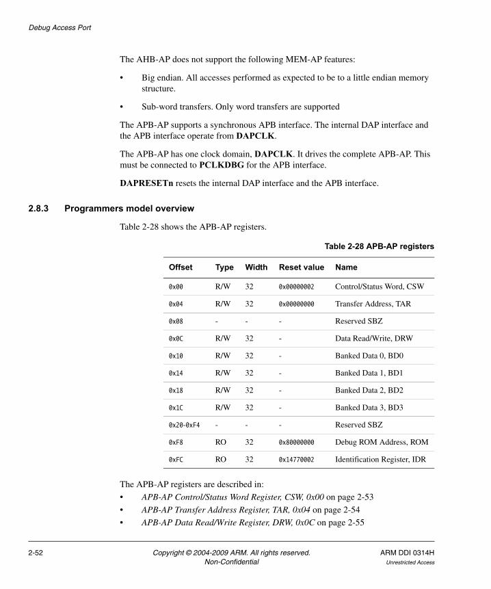
Debug Access Port
The AHB-AP does not support the following MEM-AP features:
• Big endian. All accesses performed as expected to be to a little endian memory structure.
• Sub-word transfers. Only word transfers are supported
The APB-AP supports a synchronous APB interface. The internal DAP interface and the APB interface operate from DAPCLK.
The APB-AP has one clock domain, DAPCLK. It drives the complete APB-AP. This must be connected to PCLKDBG for the APB interface.
DAPRESETn resets the internal DAP interface and the APB interface.
2.8.3 Programmers model overview
Table 2-28 shows the APB-AP registers.
The APB-AP registers are described in:
• APB-AP Control/Status Word Register, CSW, 0x00 on page 2-53
• APB-AP Transfer Address Register, TAR, 0x04 on page 2-54
• APB-AP Data Read/Write Register, DRW, 0x0C on page 2-55
Table 2-28 APB-AP registers
Offset Type Width Reset value Name
0x00 R/W 32 0x00000002 Control/Status Word, CSW
0x04 R/W 32 0x00000000 Transfer Address, TAR
0x08 - - - Reserved SBZ
0x0C R/W 32 - Data Read/Write, DRW
0x10 R/W 32 - Banked Data 0, BD0
0x14 R/W 32 - Banked Data 1, BD1
0x18 R/W 32 - Banked Data 2, BD2
0x1C R/W 32 - Banked Data 3, BD3
0x20-0xF4 - - - Reserved SBZ
0xF8 RO 32 0x80000000 Debug ROM Address, ROM
0xFC RO 32 0x14770002 Identification Register, IDR
2-52 Copyright © 2004-2009 ARM. All rights reserved. ARM DDI 0314HNon-Confidential Unrestricted Access
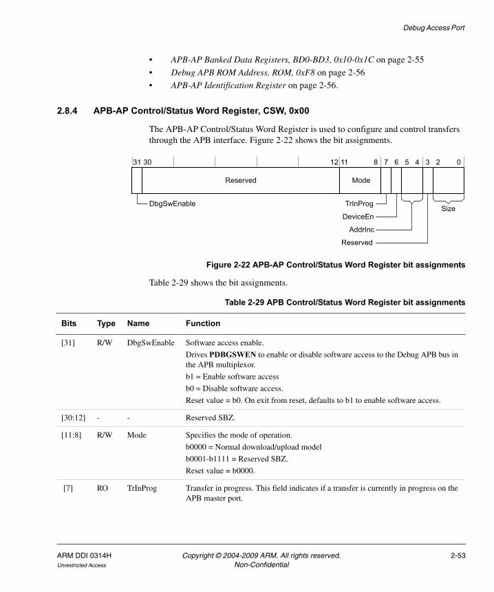
Debug Access Port
• APB-AP Banked Data Registers, BD0-BD3, 0x10-0x1C on page 2-55
• Debug APB ROM Address, ROM, 0xF8 on page 2-56
• APB-AP Identification Register on page 2-56.
2.8.4 APB-AP Control/Status Word Register, CSW, 0x00
The APB-AP Control/Status Word Register is used to configure and control transfers through the APB interface. Figure 2-22 shows the bit assignments.
Figure 2-22 APB-AP Control/Status Word Register bit assignments
Table 2-29 shows the bit assignments.
31 30 12 11 8 7 6 5 4 3 2
DbgSwEnable
Reserved Mode
0
SizeTrInProg
DeviceEn
AddrInc
Reserved
Table 2-29 APB Control/Status Word Register bit assignments
Bits Type Name Function
[31] R/W DbgSwEnable Software access enable.
Drives PDBGSWEN to enable or disable software access to the Debug APB bus in the APB multiplexor.
b1 = Enable software access
b0 = Disable software access.
Reset value = b0. On exit from reset, defaults to b1 to enable software access.
[30:12] - - Reserved SBZ.
[11:8] R/W Mode Specifies the mode of operation.
b0000 = Normal download/upload model
b0001-b1111 = Reserved SBZ.
Reset value = b0000.
[7] RO TrInProg Transfer in progress. This field indicates if a transfer is currently in progress on the APB master port.
ARM DDI 0314H Copyright © 2004-2009 ARM. All rights reserved. 2-53Unrestricted Access Non-Confidential
Debug Access Port
2.8.5 APB-AP Transfer Address Register, TAR, 0x04
The Transfer Address Register holds the address of the current transfer. Figure 2-23 on page 2-55 shows the bit assignments.
[6] RO DeviceEn Indicates the status of the DEVICEEN input.
• If APB-AP is connected to the Debug APB, that is, a bus connected only to debug and trace components, it must be permanently enabled by tying DEVICEEN HIGH. This ensures that trace components can still be programmed when DBGEN is LOW. In practice, it is expected that the APB-AP is almost always used in this way.
• If APB-AP is connected to a system APB dedicated to the non-secure world, DEVICEEN must be connected to DBGEN.
• If APB-AP is connected to a system APB dedicated to the secure world, DEVICEEN must be connected to SPIDEN.
[5:4] R/W AddrInc Auto address increment and packing mode on Read or Write data access. Does not increment if the transaction completes with an error response or the transaction is aborted.
Auto address incrementing is not performed on access to banked data registers 0x10-0x1C.
The status of these bits is ignored in these cases.
b11 = Reserved
b10 = Reserved
b01 = Increment
b00 = Auto increment OFF.
Increment occurs in word steps.
Reset value = b00.
[3] - - Reserved SBZ.
[2:0] RO Size Size of the access to perform.
Fixed at b010 = 32 bits.
Reset value = b010.
Table 2-29 APB Control/Status Word Register bit assignments (continued)
Bits Type Name Function
2-54 Copyright © 2004-2009 ARM. All rights reserved. ARM DDI 0314HNon-Confidential Unrestricted Access
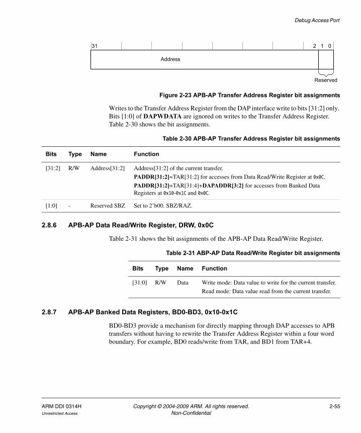
Debug Access Port
Figure 2-23 APB-AP Transfer Address Register bit assignments
Writes to the Transfer Address Register from the DAP interface write to bits [31:2] only. Bits [1:0] of DAPWDATA are ignored on writes to the Transfer Address Register. Table 2-30 shows the bit assignments.
2.8.6 APB-AP Data Read/Write Register, DRW, 0x0C
Table 2-31 shows the bit assignments of the APB-AP Data Read/Write Register.
2.8.7 APB-AP Banked Data Registers, BD0-BD3, 0x10-0x1C
BD0-BD3 provide a mechanism for directly mapping through DAP accesses to APB transfers without having to rewrite the Transfer Address Register within a four word boundary. For example, BD0 reads/write from TAR, and BD1 from TAR+4.
31 2 1
Address
0
Reserved
Table 2-30 APB-AP Transfer Address Register bit assignments
Bits Type Name Function
[31:2] R/W Address[31:2] Address[31:2] of the current transfer.
PADDR[31:2]=TAR[31:2] for accesses from Data Read/Write Register at 0x0C.
PADDR[31:2]=TAR[31:4]+DAPADDR[3:2] for accesses from Banked Data Registers at 0x10-0x1C and 0x0C.
[1:0] - Reserved SBZ Set to 2’b00. SBZ/RAZ.
Table 2-31 ABP-AP Data Read/Write Register bit assignments
Bits Type Name Function
[31:0] R/W Data Write mode: Data value to write for the current transfer.
Read mode: Data value read from the current transfer.
ARM DDI 0314H Copyright © 2004-2009 ARM. All rights reserved. 2-55Unrestricted Access Non-Confidential
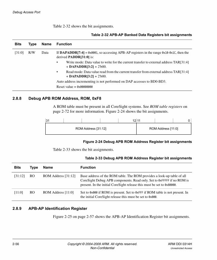
Debug Access Port
Table 2-32 shows the bit assignments.
2.8.8 Debug APB ROM Address, ROM, 0xF8
A ROM table must be present in all CoreSight systems. See ROM table registers on page 2-72 for more information. Figure 2-24 shows the bit assignments.
Figure 2-24 Debug APB ROM Address Register bit assignments
Table 2-33 shows the bit assignments.
2.8.9 APB-AP Identification Register
Figure 2-25 on page 2-57 shows the APB-AP Identification Register bit assignments.
Table 2-32 APB-AP Banked Data Registers bit assignments
Bits Type Name Function
[31:0] R/W Data If DAPADDR[7:4] = 0x0001, so accessing APB-AP registers in the range 0x10-0x1C, then the derived PADDR[31:0] is:
• Write mode: Data value to write for the current transfer to external address TAR[31:4] + DAPADDR[3:2] + 2'b00.
• Read mode: Data value read from the current transfer from external address TAR[31:4] + DAPADDR[3:2] + 2'b00.
Auto address incrementing is not performed on DAP accesses to BD0-BD3.
Reset value = 0x00000000
31 12 11 0
ROM Address [31:12] ROM Address [11:0]
Table 2-33 Debug APB ROM Address Register bit assignments
Bits Type Name Function
[31:12] RO ROM Address [31:12] Base address of the ROM table. The ROM provides a look-up table of all CoreSight Debug APB components. Read only. Set to 0xFFFFF if no ROM is present. In the initial CoreSight release this must be set to 0x80000.
[11:0] RO ROM Address [11:0] Set to 0x000 if ROM is present. Set to 0xFFF if ROM table is not present. In the initial CoreSight release this must be set to 0x000.
2-56 Copyright © 2004-2009 ARM. All rights reserved. ARM DDI 0314HNon-Confidential Unrestricted Access
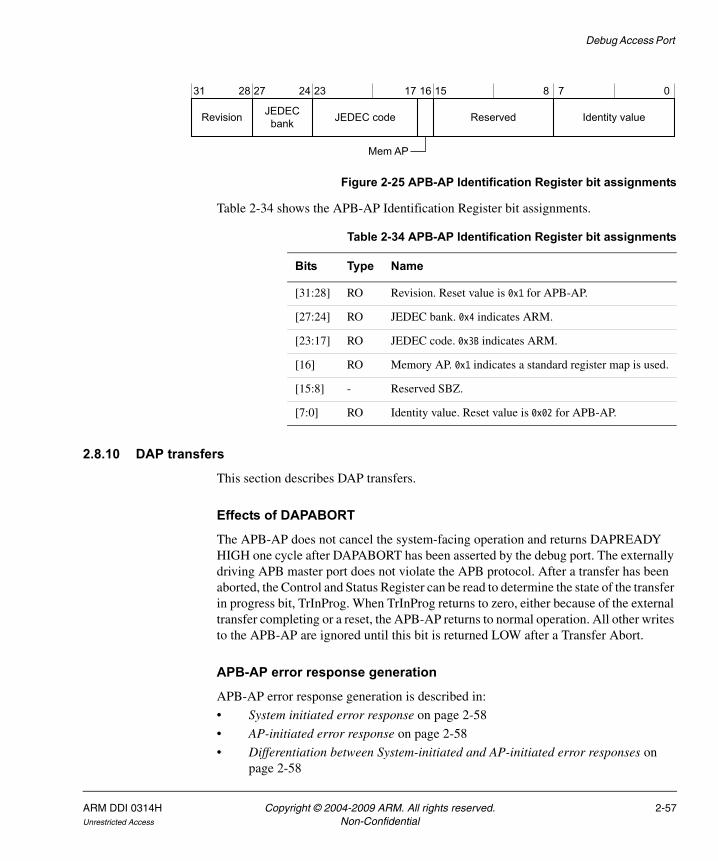
Debug Access Port
Figure 2-25 APB-AP Identification Register bit assignments
Table 2-34 shows the APB-AP Identification Register bit assignments.
2.8.10 DAP transfers
This section describes DAP transfers.
Effects of DAPABORT
The APB-AP does not cancel the system-facing operation and returns DAPREADY HIGH one cycle after DAPABORT has been asserted by the debug port. The externally driving APB master port does not violate the APB protocol. After a transfer has been aborted, the Control and Status Register can be read to determine the state of the transfer in progress bit, TrInProg. When TrInProg returns to zero, either because of the external transfer completing or a reset, the APB-AP returns to normal operation. All other writes to the APB-AP are ignored until this bit is returned LOW after a Transfer Abort.
APB-AP error response generation
APB-AP error response generation is described in:
• System initiated error response on page 2-58
• AP-initiated error response on page 2-58
• Differentiation between System-initiated and AP-initiated error responses on page 2-58
Revision
31 28 27 24 23 17 16 15 8 7 0
JEDEC bank JEDEC code Reserved Identity value
Mem AP
Table 2-34 APB-AP Identification Register bit assignments
Bits Type Name
[31:28] RO Revision. Reset value is 0x1 for APB-AP.
[27:24] RO JEDEC bank. 0x4 indicates ARM.
[23:17] RO JEDEC code. 0x3B indicates ARM.
[16] RO Memory AP. 0x1 indicates a standard register map is used.
[15:8] - Reserved SBZ.
[7:0] RO Identity value. Reset value is 0x02 for APB-AP.
ARM DDI 0314H Copyright © 2004-2009 ARM. All rights reserved. 2-57Unrestricted Access Non-Confidential
Debug Access Port
System initiated error response
An error response received on the APB master interface propagates onto the DAP bus as the transfer is completed. This is received by the debug ports.
AP-initiated error response
• APB-AP reads after an abort:
After a Transfer Abort operation has been carried out, and an external transfer is still pending, that is, the TrInProg bit in the Control/Status Word Register is still HIGH, reads of all registers return a normal response except for reads of the data registers Data Read/Write Register and banked registers which cannot initiate a new system read transfer. Reads of the Data Read/Write Register and banked registers return an error response until the TrInProg bit is cleared because of the system transfer completing, or a reset.
• APB-AP writes after an abort:
After a Transfer Abort operation has been carried out, and an external transfer is still pending, that is, the transfer in progress bit is still HIGH, all writes to the access port return an error response, because they are ignored until the TrInProg bit has cleared.
Differentiation between System-initiated and AP-initiated error responses
If DAPSLVERR is HIGH and TrInProg is LOW in the Control/Status Word Register then the error is from a system error response.
If DAPSLVERR is HIGH and TrInProg is HIGH, then the error is from an access port error response. The transfer has not been accepted by the access port. This case can only occur after an abort has been initiated and the system transfer has not completed.
2-58 Copyright © 2004-2009 ARM. All rights reserved. ARM DDI 0314HNon-Confidential Unrestricted Access
Debug Access Port
2.9 JTAG-APThe JTAG Access Port (JTAG-AP) provides JTAG access to on-chip components, operating as a JTAG master port to drive JTAG chains throughout a SoC. The JTAG command protocol is byte-orientated, with a word wrapper on the read and write ports to yield acceptable performance from the DAP internal bus which has a 32-bit data path only. Daisy chaining is avoided by using a port multiplexor. In this way, slower cores do not impede faster cores. For more information about the JTAG-AP, see the description of the JTAG-AP in the ARM Debug Interface v5 Architecture Specification and the ARM Debug Interface v5.1 Architecture Supplement.
The implementation specific features of the JTAG-AP is described in the following sections
• External interfaces
• RTCK connections on page 2-60
• Programmers model overview on page 2-61
2.9.1 External interfaces
Table 2-35 shows the JTAG to slave device signals.
Each o f the eight JTAG scan chains are on the same bit positions for each JTAG signal. For example, connections for scan chain 0 can be located on bit [0] of each bus connection of CSTCK, CSTMS, CSTDI, PORTCONNECTED.
Table 2-35 JTAG to slave device signals
Name Type Description
nSRSTOUT[7:0] Output Subsystem Reset Out
SRSTCONNECTED[7:0] Input Subsystem Reset is present/wired
nCSTRST[7:0] Output JTAG Test Reset
CSTCK[7:0] Output JTAG Test Clock
CSTMS[7:0] Output JTAG Test Mode Select
CSTDI[7:0] Output JTAG Test Data In, to external TAP
CSTDO[7:0] Input JTAG Test Data Out, from external TAP
ARM DDI 0314H Copyright © 2004-2009 ARM. All rights reserved. 2-59Unrestricted Access Non-Confidential
Debug Access Port
2.9.2 RTCK connections
This section describes the RTCK connections.
Global port and RTCK
When more than one bit of PORTSEL[7:0] is set, all active JTAG-AP multiplexor port RTCKs are combinatorially joined, so that:
• If TCK=0 then select OR of active RTCKs
• TCK=1 then select AND of active RTCKs.
An active RTCK is generated by an active port which is defined as a port which:
• is selected, when its PORTSEL[7:0] bit is set
• is connected, when its PORTCONNECTED[7:0] bit is set
• has not been disabled or powered down in this session, when its PSTA bit is 0.
If no ports are active, RTCK is connected directly to TCK. This means that disabling or powering down a JTAG slave cannot lock up the RTCK interface.
Asynchronous TAP controllers which do not require an RTCK connection should connect their TCK output from JTAG-AP to the corresponding RTCK input.
RTCK wrapper
Note This section applies only to synchronous TAP controllers.
Where devices do not have a return clock, a RTCK wrapper must be used to register TCK against the processor clock. See the CoreSight Components Implementation Guide and the applicable Integration Manual for details on how to implement an RTCK wrapper.
CSRTCK[7:0] Input Return Test Clock, target pacing signal
PORTCONNECTED[7:0] Input JTAG Port is connected, status signal
PORTENABLED[7:0] Input JTAG Port is enabled, for example, it might be deasserted by a processor powering down
Table 2-35 JTAG to slave device signals (continued)
Name Type Description
2-60 Copyright © 2004-2009 ARM. All rights reserved. ARM DDI 0314HNon-Confidential Unrestricted Access
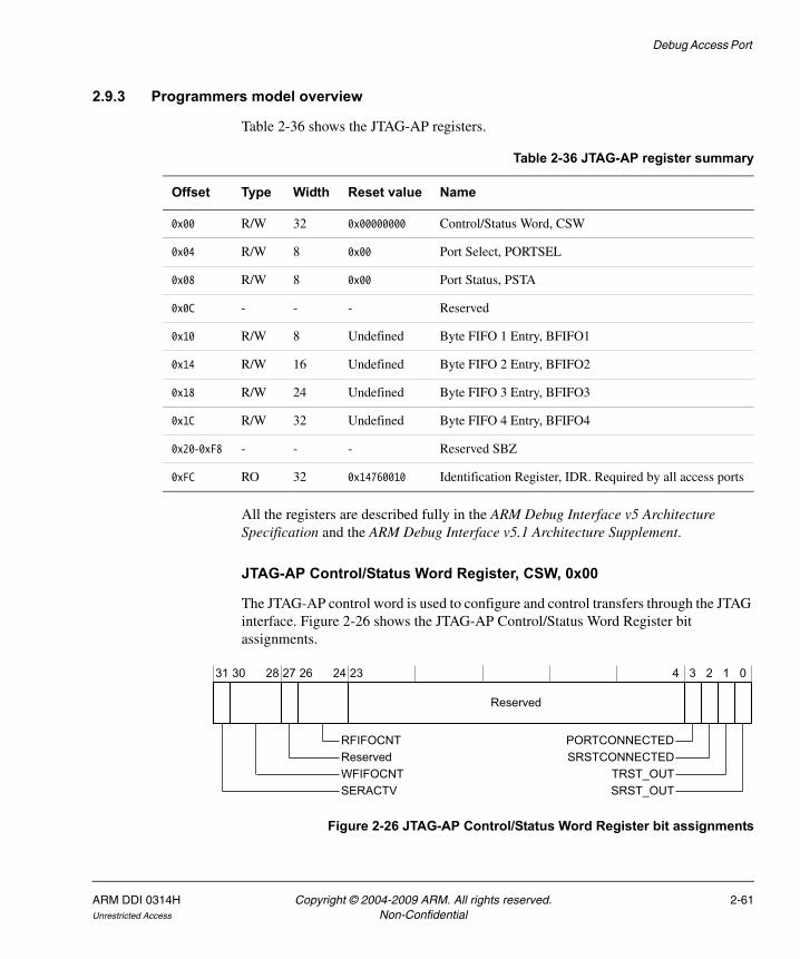
Debug Access Port
2.9.3 Programmers model overview
Table 2-36 shows the JTAG-AP registers.
All the registers are described fully in the ARM Debug Interface v5 Architecture Specification and the ARM Debug Interface v5.1 Architecture Supplement.
JTAG-AP Control/Status Word Register, CSW, 0x00
The JTAG-AP control word is used to configure and control transfers through the JTAG interface. Figure 2-26 shows the JTAG-AP Control/Status Word Register bit assignments.
Figure 2-26 JTAG-AP Control/Status Word Register bit assignments
Table 2-36 JTAG-AP register summary
Offset Type Width Reset value Name
0x00 R/W 32 0x00000000 Control/Status Word, CSW
0x04 R/W 8 0x00 Port Select, PORTSEL
0x08 R/W 8 0x00 Port Status, PSTA
0x0C - - - Reserved
0x10 R/W 8 Undefined Byte FIFO 1 Entry, BFIFO1
0x14 R/W 16 Undefined Byte FIFO 2 Entry, BFIFO2
0x18 R/W 24 Undefined Byte FIFO 3 Entry, BFIFO3
0x1C R/W 32 Undefined Byte FIFO 4 Entry, BFIFO4
0x20-0xF8 - - - Reserved SBZ
0xFC RO 32 0x14760010 Identification Register, IDR. Required by all access ports
31 30 28 27 26 24 23 4 3 2 1 0
Reserved
RFIFOCNTReservedWFIFOCNTSERACTV
PORTCONNECTEDSRSTCONNECTED
TRST_OUTSRST_OUT
ARM DDI 0314H Copyright © 2004-2009 ARM. All rights reserved. 2-61Unrestricted Access Non-Confidential

Debug Access Port
Table 2-37 shows the JTAG-AP Control/Status Word Register bit assignments. The register must not be modified while there are outstanding commands in the Write FIFO.
JTAG-AP Port Select Register, PORTSEL, 0x04
The Port Select Register enables ports if connected and the slave port is currently enabled. The Port Select Register must be written when the TCK engine is idle, SERACTV=0, and WFIFO, WFIFOCNT=0, is empty. Writing at other times can generate unpredictable results.
Figure 2-27 shows the shows the JTAG-AP Port Select Register bit assignments.
Table 2-37 JTAG-AP Control/Status Word Register bit assignments
Bits Type Name Function
[31] RO SERACTV JTAG Serializer active.
Reset value = b0.
[30:28] RO WFIFOCNT Outstanding Write FIFO Byte Count.
Reset value = b000.
[27] - - Reserved SBZ
[26:24] RO RFIFOCNT Outstanding Read FIFO Byte Count.
Reset value = b000
[23:4] - - Reserved SBZ 0x00000
[3] RO PORTCONNECTED PORT Connected. AND of PORTCONNECTED inputs of currently selected ports.Reset value = b0.
[2] RO SRSTCONNECTEDa SRST Connected.
AND of SRSTCONNECTED inputs of currently selected ports. If multiple ports are selected, it is the AND of all the SRSTCONNECTED inputs from the selected ports.
Reset value = b0.
[1] R/W TRST_OUT TRST Assert, not self clearing.
JTAG TAP controller reset.
Reset value = b0.
[0] R/W SRST_OUT SRST Assert, not self clearing.
Core Reset.
Reset value = b0.
a. SRSTCONNECTED is a strap pin on the multiplexor inputs. It is set to 1 to indicate that the target JTAG device supports individual SRST controls.
2-62 Copyright © 2004-2009 ARM. All rights reserved. ARM DDI 0314HNon-Confidential Unrestricted Access
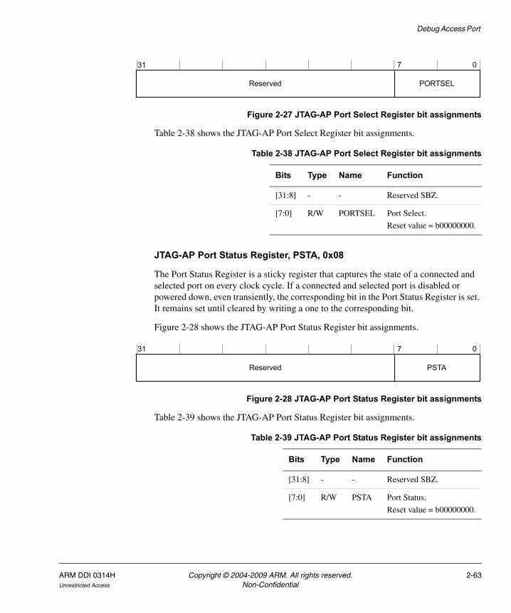
Debug Access Port
Figure 2-27 JTAG-AP Port Select Register bit assignments
Table 2-38 shows the JTAG-AP Port Select Register bit assignments.
JTAG-AP Port Status Register, PSTA, 0x08
The Port Status Register is a sticky register that captures the state of a connected and selected port on every clock cycle. If a connected and selected port is disabled or powered down, even transiently, the corresponding bit in the Port Status Register is set. It remains set until cleared by writing a one to the corresponding bit.
Figure 2-28 shows the JTAG-AP Port Status Register bit assignments.
Figure 2-28 JTAG-AP Port Status Register bit assignments
Table 2-39 shows the JTAG-AP Port Status Register bit assignments.
0
PORTSEL
7
Reserved
31
Table 2-38 JTAG-AP Port Select Register bit assignments
Bits Type Name Function
[31:8] - - Reserved SBZ.
[7:0] R/W PORTSEL Port Select.
Reset value = b00000000.
0
PSTA
7
Reserved
31
Table 2-39 JTAG-AP Port Status Register bit assignments
Bits Type Name Function
[31:8] - - Reserved SBZ.
[7:0] R/W PSTA Port Status.
Reset value = b00000000.
ARM DDI 0314H Copyright © 2004-2009 ARM. All rights reserved. 2-63Unrestricted Access Non-Confidential

Debug Access Port
JTAG-AP Byte FIFO registers, BFIFOn, 0x10-0x1C
The Byte FIFO registers are a word interface to one, two, three, or four parallel byte entries in the Byte Command FIFO, LSB first. The DAP Internal Bus is a 32-bit interface with no SIZE field. So, an address decoding is used to designate size, because the JTAG-AP Engine JTAG protocol is byte encoded. Writes to the BFIFOx larger than the current write FIFO depth stall on DAPREADY in Normal mode. Reads to the BFIFOx larger than the current read FIFO depth stall on DAPREADY in Normal mode. For reads less than the full 32-bits, the upper bits are zero. For example, for a 24-bit read, DAPRDATA[31:24] is 0x00.
JTAG-AP Identification Register
Figure 2-29 shows the JTAG-AP Identification Register bit assignments.
Figure 2-29 JTAG-AP Identification Register bit assignments
Table 2-40 shows the JTAG-AP Identification Register bit assignments.
Revision
31 28 27 24 23 17 16 15 8 7 0
JEDEC bank JEDEC code Reserved Identity value
Mem AP
Table 2-40 JTAG-AP Identification Register bit assignments
Bits Type Name Value Meaning
[31:28] RO Revision 0x3 Revision 3
[27:24] RO JEDEC bank 0x4 Designed by ARM
[23:17] RO JEDEC code 0x3B Designed by ARM
[16] RO Mem AP 0x0 Is a Mem AP
[15:8] - Reserved 0x00 -
[7:0] RO Identity value 0x10 JTAG-AP
2-64 Copyright © 2004-2009 ARM. All rights reserved. ARM DDI 0314HNon-Confidential Unrestricted Access
Debug Access Port
2.10 Auxiliary Access PortAn auxiliary interface is supplied to enable connecting to the access port of processors that have a compliant debug interface, such as the Cortex-M3. This interface is selected when the APSelect bits (bits [31:24] of the SELECT register in the Debug Port) are set to 0x03.
If this interface is not used then reads to the AP Identification Register (IDR) return 0x00000000, which indicates that no AP is present. See the applicable Integration Manual for more details of wiring this interface when not required. For more information on reading the IDR, see the ARM Debug Interface v5 Architecture Specification and the ARM Debug Interface v5.1 Architecture Supplement.
ARM DDI 0314H Copyright © 2004-2009 ARM. All rights reserved. 2-65Unrestricted Access Non-Confidential
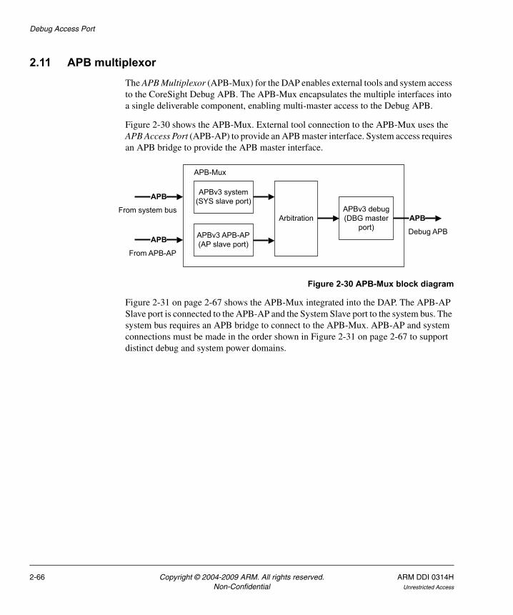
Debug Access Port
2.11 APB multiplexorThe APB Multiplexor (APB-Mux) for the DAP enables external tools and system access to the CoreSight Debug APB. The APB-Mux encapsulates the multiple interfaces into a single deliverable component, enabling multi-master access to the Debug APB.
Figure 2-30 shows the APB-Mux. External tool connection to the APB-Mux uses the APB Access Port (APB-AP) to provide an APB master interface. System access requires an APB bridge to provide the APB master interface.
Figure 2-30 APB-Mux block diagram
Figure 2-31 on page 2-67 shows the APB-Mux integrated into the DAP. The APB-AP Slave port is connected to the APB-AP and the System Slave port to the system bus. The system bus requires an APB bridge to connect to the APB-Mux. APB-AP and system connections must be made in the order shown in Figure 2-31 on page 2-67 to support distinct debug and system power domains.
APBv3 system (SYS slave port)
APBv3 APB-AP (AP slave port)
APBv3 debug(DBG master
port)Arbitration APB
APB
APB
APB-Mux
From system bus
From APB-AP
Debug APB
2-66 Copyright © 2004-2009 ARM. All rights reserved. ARM DDI 0314HNon-Confidential Unrestricted Access
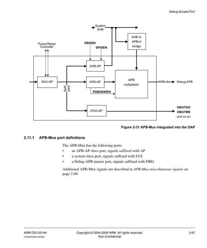
Debug Access Port
Figure 2-31 APB-Mux integrated into the DAP
2.11.1 APB-Mux port definitions
The APB-Mux has the following ports:
• an APB-AP slave port, signals suffixed with AP
• a system slave port, signals suffixed with SYS
• a Debug APB master port, signals suffixed with DBG.
Additional APB-Mux signals are described in APB-Mux miscellaneous signals on page 2-68.
SWJ-DP APBmultiplexer
AHB-AP
APB-AP
SPIDENDBGEN
JTAG-AP
PDBGSWEN
DA
PA
PB
Power/ResetController
AHB toAPBv3bridge
Debug APBAPBv3
DBGTDODBGTMSand so on
SystemAHB
ARM DDI 0314H Copyright © 2004-2009 ARM. All rights reserved. 2-67Unrestricted Access Non-Confidential
Debug Access Port
2.11.2 APB-Mux miscellaneous signals
Table 2-41 shows the APB-Mux miscellaneous signals.
2.11.3 APB-Mux arbitration and APB Mux connectivity
This section describes APB-Mux arbitration and connectivity:
• APB-Mux arbitration
• APB-Mux connectivity on page 2-69.
APB-Mux arbitration
The APB-Mux uses a fixed arbitration scheme to support the two slave interfaces. The arbitration logic ensures that only one APB bus master, either the APB-AP, or system bus master has access to the CoreSight Debug APB at any one time.
The APB-AP Slave port always has priority over the System Slave port. If two transfers are initiated at the same time, the transfer from the APB-AP Slave port is always propagated to the master port output for Debug APB access. The System Slave port is only granted access if the APB-AP Slave port is not requesting an access, that is, PSELAP is LOW. It is therefore possible for the APB-AP Slave port to maintain back-to-back transfers on the Debug APB without allowing access to the System Slave port. When a transaction is in progress on one slave port and the other port initiates a transaction, PREADY is held LOW for the newly requested transaction until the APB-Mux arbiter grants access to the other slave port.
The APB-Mux provides no address decoding, nor default response generation. This must be implemented by an external address decoder incorporating a default slave.
Table 2-41 APB-Mux miscellaneous signals
Name Type Description
nCDBGPWRDN Input Indicates that the debug infrastructure is powered down. Any system accesses to the debug APB return an error response. Also enables clamping of signals driven onto the system interface, and clamping of inputs to the debug domain.
nCSOCPWRDN Input Indicates that the system APB slave interface is powered down and enables clamping of signals driven into the APB Mux. Also clamps inputs to the system domain.
PDBGSWEN Input Enables software access to the Debug APB.
2-68 Copyright © 2004-2009 ARM. All rights reserved. ARM DDI 0314HNon-Confidential Unrestricted Access
Debug Access Port
APB-Mux connectivity
The connection rules are:
• AP-AP Slave port connects to the APB-AP
• System Slave port connects to the system bus.
2.11.4 APB-Mux Software Access Enable
The APB-Mux receives PDBGSWEN from the APB-AP to enable software access from the System Slave Port to the Debug APB.
PDBGSWEN LOW
System access to the Debug APB is not permitted. The System Slave port must return PSLVERRSYS HIGH on any access. No APB-Mux master transfer is initiated.
PDBGSWEN HIGH
System access to the Debug APB is permitted.
2.11.5 APB-Mux clocks, power, and resets
The APB-Mux has two clocks:
PCLKDBG Drives all logic, except for the System Slave port interface.
PCLKSYS Drives the System Slave port interface.
The APB-Mux has an asynchronous interface between the System Slave port and the rest of the APB-Mux, as shown in Figure 2-32 on page 2-70. The asynchronous interface defines a common boundary between:
• debug and system clocks domains, PCLKDBG and PCLKSYS• debug and system reset domains, PRESETDBGn and PRESETSYSn• debug and system power domains.
ARM DDI 0314H Copyright © 2004-2009 ARM. All rights reserved. 2-69Unrestricted Access Non-Confidential
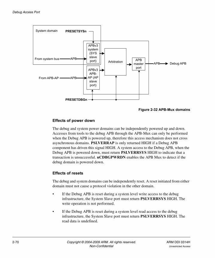
Debug Access Port
Figure 2-32 APB-Mux domains
Effects of power down
The debug and system power domains can be independently powered up and down. Accesses from tools to the debug APB through the APB-Mux can only be performed when the Debug APB is powered up, therefore this access mechanism does not cross asynchronous domains. PSLVERRAP is only returned HIGH if a Debug APB component has driven this signal HIGH. A system access to the Debug APB, when the Debug APB is powered down, must return PSLVERRSYS HIGH to indicate that a transaction is unsuccessful. nCDBGPWRDN enables the APB Mux to detect if the debug domain is powered down.
Effects of resets
The debug and system domains can be independently reset. A reset initiated from either domain must not cause a protocol violation in the other domain.
• If the Debug APB is reset during a system level write access to the debug infrastructure, the System Slave port must return PSLVERRSYS HIGH. The write operation is not performed.
• If the Debug APB is reset during a system level read access to the debug infrastructure, the System Slave port must return PSLVERRSYS HIGH. The read data is undefined.
PRESETDBGn
PRESETSYSn
APBv3 system(SYS slave port)
APBv3 APB-
AP (AP slave port)
Arbitration APB master
port
APB
APB
From APB-AP
From system busDebug APB
System domain
APB
2-70 Copyright © 2004-2009 ARM. All rights reserved. ARM DDI 0314HNon-Confidential Unrestricted Access
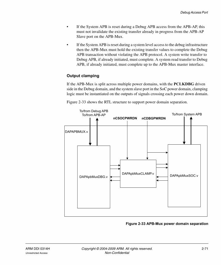
Debug Access Port
• If the System APB is reset during a Debug APB access from the APB-AP, this must not invalidate the existing transfer already in progress from the APB-AP Slave port on the APB-Mux.
• If the System APB is reset during a system level access to the debug infrastructure then the APB-Mux must hold the existing transfer values to complete the Debug APB transaction without violating the APB protocol. A system write transfer to Debug APB, if already initiated, must complete. A system read transfer to Debug APB, if already initiated, must complete up to the APB-Mux master interface.
Output clamping
If the APB-Mux is split across multiple power domains, with the PCLKDBG driven side in the Debug domain, and the system slave port in the SoC power domain, clamping logic must be instantiated on the outputs of signals crossing each power down domain.
Figure 2-33 shows the RTL structure to support power domain separation.
Figure 2-33 APB-Mux power domain separation
DAPAPBMUX.v
DAPApbMuxDBG.v DAPApbMuxSOC.vDAPApbMuxCLAMP.v
To/from System APBTo/from Debug APB
To/from APB-APnCSOCPWRDN nCDBGPWRDN
ARM DDI 0314H Copyright © 2004-2009 ARM. All rights reserved. 2-71Unrestricted Access Non-Confidential
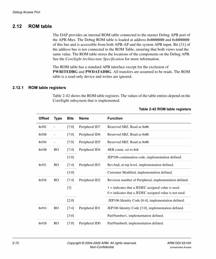
Debug Access Port
2.12 ROM tableThe DAP provides an internal ROM table connected to the master Debug APB port of the APB-Mux. The Debug ROM table is loaded at address 0x00000000 and 0x80000000 of this bus and is accessible from both APB-AP and the system APB input. Bit [31] of the address bus is not connected to the ROM Table, ensuring that both views read the same value. The ROM table stores the locations of the components on the Debug APB. See the CoreSight Architecture Specification for more information.
The ROM table has a standard APB interface except for the exclusion of PWRITEDBG and PWDATADBG. All transfers are assumed to be reads. The ROM table is a read-only device and writes are ignored.
2.12.1 ROM table registers
Table 2-42 shows the ROM table registers. The values of the table entries depend on the CoreSight subsystem that is implemented.
Table 2-42 ROM table registers
Offset Type Bits Name Function
0xFDC - [7:0] Peripheral ID7 Reserved SBZ. Read as 0x00.
0xFD8 - [7:0] Peripheral ID6 Reserved SBZ. Read as 0x00.
0xFD4 - [7:0] Peripheral ID5 Reserved SBZ. Read as 0x00.
0xFD0 RO [7:4] Peripheral ID4 4KB count, set to 0x0.
[3:0] JEP106 continuation code, implementation defined.
0xFEC RO [7:4] Peripheral ID3 RevAnd, at top level, implementation defined.
[3:0] Customer Modified, implementation defined.
0xFE8 RO [7:4] Peripheral ID2 Revision number of Peripheral, implementation defined.
[3] 1 = indicates that a JEDEC assigned value is used.
0 = indicates that a JEDEC assigned value is not used.
[2:0] JEP106 Identity Code [6:4], implementation defined.
0xFE4 RO [7:4] Peripheral ID1 JEP106 Identity Code [3:0], implementation defined.
[3:0] PartNumber1, implementation defined.
0xFE0 RO [7:0] Peripheral ID0 PartNumber0, implementation defined.
2-72 Copyright © 2004-2009 ARM. All rights reserved. ARM DDI 0314HNon-Confidential Unrestricted Access

Debug Access Port
The ROM table has a specific PrimeCell class. In all registers 0xFD0-0xFFC, bits [31:8] are reserved and should be read as zero. Locations 0xF00-0xFCC are reserved and should be read as zero.
2.12.2 ROM table entries
Table 2-43 shows the ROM table entries bit assignments for each entry in the 0x000-0xEFC region.
The last entry in the ROM table has the value 0x00000000, which is reserved.If the CoreSight component occupies several consecutive 4KB blocks, the base address of the lowest block in memory is given. The locations of components are stored in sequential locations with the ROM table. The entry following the last component in the table must read 0x00000000, and subsequent locations are assumed to read as zero.
0xFF0 RO [7:0] Component ID0 Preamble. Set to 0x0D.
0xFF4 RO [7:0] Component ID1 Preamble. Set to 0x10.
0xFF8 RO [7:0] Component ID2 Preamble. Set to 0x05.
0xFFC RO [7:0] Component ID3 Preamble. Set to 0xB1.
Table 2-42 ROM table registers (continued)
Offset Type Bits Name Function
Table 2-43 ROM table entries bit assignments
Bits Name Description
[31:12] Address offset Base address of the component, relative to the ROM address. Negative values are permitted using two's complement.
ComponentAddress = ROMAddress + (AddressOffset SHL 12).
[11:2] - Reserved SBZ.
[1] Format 1 = 32-bit format. In the DAP Debug ROM this is set to 1.
0 = 8-bit format.
[0] Entry present Set HIGH to indicate an entry is present.
ARM DDI 0314H Copyright © 2004-2009 ARM. All rights reserved. 2-73Unrestricted Access Non-Confidential
Debug Access Port
2.13 Authentication requirements for Debug Access PortThis section describes the functionality that must be available in the debug and trace components to permit authentication using the signals, and describes how they must be connected. If you do not require the system to support this level of control, you can simplify the system design.
The full authentication requirements are defined in the CoreSight Architecture Specification.
APB-AP has one authentication signal, called DEVICEEN:
• If the APB-AP is connected to a debug bus, this signal must be tied HIGH. In this release of the CoreSight Design Kit, the APB-AP must be connected to a debug bus, and DEVICEEN must be tied HIGH.
• If the APB-AP is connected to a system bus dedicated to the secure world, this signal must be connected to SPIDEN.
• If the APB-AP is connected to a system bus dedicated to the non-secure world, this signal must be connected to DBGEN.
For more information about SPIDEN and DBGEN, see the CoreSight Architecture Specification.
2-74 Copyright © 2004-2009 ARM. All rights reserved. ARM DDI 0314HNon-Confidential Unrestricted Access
Debug Access Port
2.14 Clocks, power, and resetsThe DAP implements 4 clock and power domains they are:
• Debug Port interface domain, driven by SWCLKTCK, which governs the Serial Wire and JTAG Debug Ports
• Debug Domain, covering the internal bus communication of the DAP, the APB-AP and the dedicated Debug APB, based on PCLKDBG
• AHB system domain, clocked by HCLK, is the AHB-Lite master interface on AHB-AP
• APB system domain, clocked by PCLKSYS on the APB slave input to the APB-MUX.
For more information on the partitioning and controlling signals for the separate clock domains, refer to the appropriate sections.
PCLKDBG must be driven by a constant clock. It must not be stopped or altered while the DAP is in use (determined by the debug power request from the Debug Port). PCLKENDBG can be used as a clock gating term to reduce the effective clock speed from PCLKDBG. PRESETDBGn initializes the state of all registers in the PCLKDBG domain. PRESETDBGn enables initialization of the DAP without affecting the normal operation of the SoC in which the DAP is integrated, and should be driven by the tools on external connection to the debug port. The reset can be initiated by writing to the control register of the Debug Port (the debug reset request register). This resets all the registers in the Debug clock domain, that is, Debug APB and DAP domains.
Note Internally to the DAP there is a clock signal which is not presented at the top level but is internally connected to PCLKDBG. Correspondingly the internal reset and clock enable terms are also connected to PRESETDBGn and PCLKENDBG respectively.
ARM DDI 0314H Copyright © 2004-2009 ARM. All rights reserved. 2-75Unrestricted Access Non-Confidential

Debug Access Port
2-76 Copyright © 2004-2009 ARM. All rights reserved. ARM DDI 0314HNon-Confidential Unrestricted Access
Chapter 3 CoreSight Trace Sources
This chapter gives an overview of two CoreSight trace sources, HTMs and ETMs. It contains the following sections:
• AMBA AHB Trace Macrocell on page 3-2
• Embedded Trace Macrocells on page 3-4.
ARM DDI 0314H Copyright © 2004-2009 ARM. All rights reserved. 3-1Unrestricted Access Non-Confidential
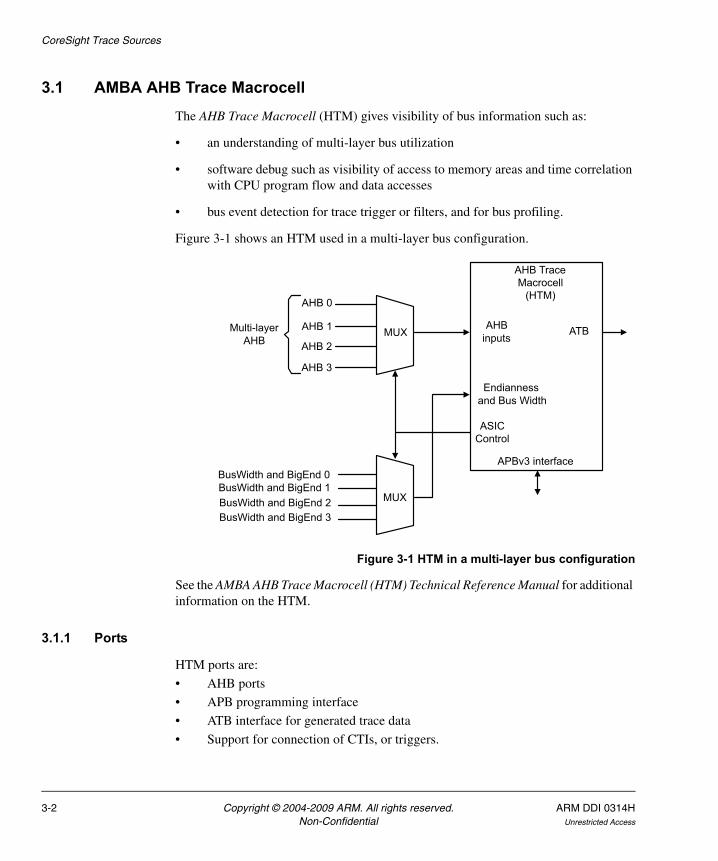
CoreSight Trace Sources
3.1 AMBA AHB Trace MacrocellThe AHB Trace Macrocell (HTM) gives visibility of bus information such as:
• an understanding of multi-layer bus utilization
• software debug such as visibility of access to memory areas and time correlation with CPU program flow and data accesses
• bus event detection for trace trigger or filters, and for bus profiling.
Figure 3-1 shows an HTM used in a multi-layer bus configuration.
Figure 3-1 HTM in a multi-layer bus configuration
See the AMBA AHB Trace Macrocell (HTM) Technical Reference Manual for additional information on the HTM.
3.1.1 Ports
HTM ports are:
• AHB ports
• APB programming interface
• ATB interface for generated trace data
• Support for connection of CTIs, or triggers.
AHB Trace Macrocell
(HTM)
Endiannessand Bus Width
APBv3 interface
ATB
ASICControl
MUXBusWidth and BigEnd 1
BusWidth and BigEnd 3BusWidth and BigEnd 2
BusWidth and BigEnd 0
AHB 0
AHB 1
AHB 2
AHB 3
MUXAHB
inputsMulti-layer
AHB
3-2 Copyright © 2004-2009 ARM. All rights reserved. ARM DDI 0314HNon-Confidential Unrestricted Access
CoreSight Trace Sources
3.1.2 Authentication requirements for the HTM
See the AMBA™ AHB Trace Macrocell (HTM) Technical Reference Manual for more information.
ARM DDI 0314H Copyright © 2004-2009 ARM. All rights reserved. 3-3Unrestricted Access Non-Confidential
CoreSight Trace Sources
3.2 Embedded Trace MacrocellsCoreSight-compliant Embedded Trace Macrocells (ETMs) provide processor-driven trace through an ATB-compliant trace port. Configuration is supported through the CoreSight APB programming interface.
3.2.1 Ports
ETM ports are:
• Core interface
• APB programming interface
• ATB interface for generation of trace data
• Support for connection of CTIs, or triggers.
Further reading on page xxiv lists publications that provide additional information on ETMs.
3-4 Copyright © 2004-2009 ARM. All rights reserved. ARM DDI 0314HNon-Confidential Unrestricted Access
Chapter 4 Embedded Cross Trigger
This chapter describes the Embedded Cross Trigger (ECT), Cross Trigger Interface (CTI), and the Cross Trigger Matrix (CTM). It contains the following sections:
• About the Embedded Cross Trigger on page 4-2
• ECT programmers model on page 4-8
• Summary of CTI registers on page 4-9
• CTI register descriptions on page 4-12
• ECT Integration Test Registers on page 4-23
• ECT CoreSight defined registers on page 4-28
• ECT connectivity recommendations on page 4-30
• ECT authentication requirements on page 4-35.
ARM DDI 0314H Copyright © 2004-2009 ARM. All rights reserved. 4-1Unrestricted Access Non-Confidential
Embedded Cross Trigger
4.1 About the Embedded Cross TriggerThe ECT for CoreSight consists of a number of CTIs and CTMs connected together. You can operate a single CTI without the requirement for a CTM.
4.1.1 How ECT works
The ECT provides an interface to the debug system as shown in Figure 4-1 on page 4-3. This enables ARM/ETM subsystems to interact, that is cross trigger, with each other. The debug system enables debug support for multiple cores, together with cross triggering between the cores and their respective ETMs.
The main function of the ECT (CTI and CTM) is to pass debug events from one core to another. For example, the ECT can communicate debug state information from one core to another, so that program execution on both processors can be stopped at the same time if required.
Cross Trigger Interface (CTI)
The CTI combines and maps the trigger requests, and broadcasts them to all other interfaces on the ECT as channel events. When the CTI receives a channel event it maps this onto a trigger output. This enables subsystems to cross trigger with each other. The receiving and transmitting of triggers is performed through the trigger interface.
Cross Trigger Matrix (CTM)
This block controls the distribution of channel events. It provides Channel Interfaces (CIs) for connection to either CTIs or CTMs. This enables multiple CTIs to be linked together.
4-2 Copyright © 2004-2009 ARM. All rights reserved. ARM DDI 0314HNon-Confidential Unrestricted Access
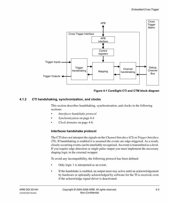
Embedded Cross Trigger
Figure 4-1 CoreSight CTI and CTM block diagram
4.1.2 CTI handshaking, synchronization, and clocks
This section describes handshaking, synchronization, and clocks in the following sections:
• Interfaces handshake protocol
• Synchronization on page 4-4
• Clock domains on page 4-6.
Interfaces handshake protocol
The CTI does not interpret the signals on the Channel Interface (CI) or Trigger Interface (TI). If handshaking is enabled it is assumed the events are edge-triggered. As a result, closely occurring events can be unreliably recognized. An event is transmitted as a level. If you require edge detection or single pulse output you must implement the necessary shaping logic in the external wrapper.
To avoid any incompatibility, the following protocol has been defined:
• Only logic 1 is interpreted as an event.
• If the handshake is enabled, an output must stay active until an acknowledgement by hardware or optionally acknowledged by software for the TI is received, even if the acknowledge signal driver is deactivated.
APB interface
Control registers
MappingChannel
handshaking
Triggerhandshaking
Cross Trigger Interface
Cross Trigger Matrix
Trigger Inputs
Trigger Outputs
Debug Channel
Bus
APB
ARM DDI 0314H Copyright © 2004-2009 ARM. All rights reserved. 4-3Unrestricted Access Non-Confidential

Embedded Cross Trigger
If the handshaking is enabled, the CTI can only handle one-shot events. If events are close to one another, or multi-shot, and mapped to the same channel they are possibly merged into one event on an output trigger. For debug events such as breakpoint, trace start, and trace stop this does not cause a problem because input events mapped to the same triggers are required to do the same thing.
Events arising from different interfaces but mapped to the same channel might also be merged. This is acceptable because the mapping logic would have been programmed to enable this. Events can be merged because blocks handshake between asynchronous clock domains or channels events are mapped onto the same output trigger.
If the events sent on the CTI emanate from the same clock domain then you can bypass the handshaking and synchronizing logic. The output does not receive an acknowledgement. In such cases you can use the CTI to transmit multiple shot events. The output has to remain active for at least one clock cycle to ensure it is captured at the destination interface.
Synchronization
Systems where events broadcast into the CTI can emanate from asynchronous clock domains must observe the following rules:
1. Register input events. Any signal that is an input to the CTI must be glitch-free to avoid any false event. The built-in synchronizers must be enabled unless external synchronization has been performed.
2. Synchronize output events on page 4-5. The outputs of the CTI must be synchronized to the local clock domain before being used by the subsystem, if such synchronization is not already present in the subsystem.
Register input events
The concern here is that a glitch on an output of the subsystem is propagated in the CTI and can be interpreted as an event. Also, the synthesis tools do not provide the necessary mechanism to constrain signals so that they are glitch free.
For example, in an ARM9E processor design, DBGACK is the output of a combinatorial circuit, that is, a three-input OR gate. There is no way to ensure that a change of state on the inputs does not result in a glitch on the DBGACK signal that can be fetched by an asynchronous circuit.
A single register can be used in this case provided the signal is in the same clock domain as the CTI. Alternatively, you can enable the synchronization logic in the CTI for that specific trigger input adding an extra clock cycle to the latency.
4-4 Copyright © 2004-2009 ARM. All rights reserved. ARM DDI 0314HNon-Confidential Unrestricted Access
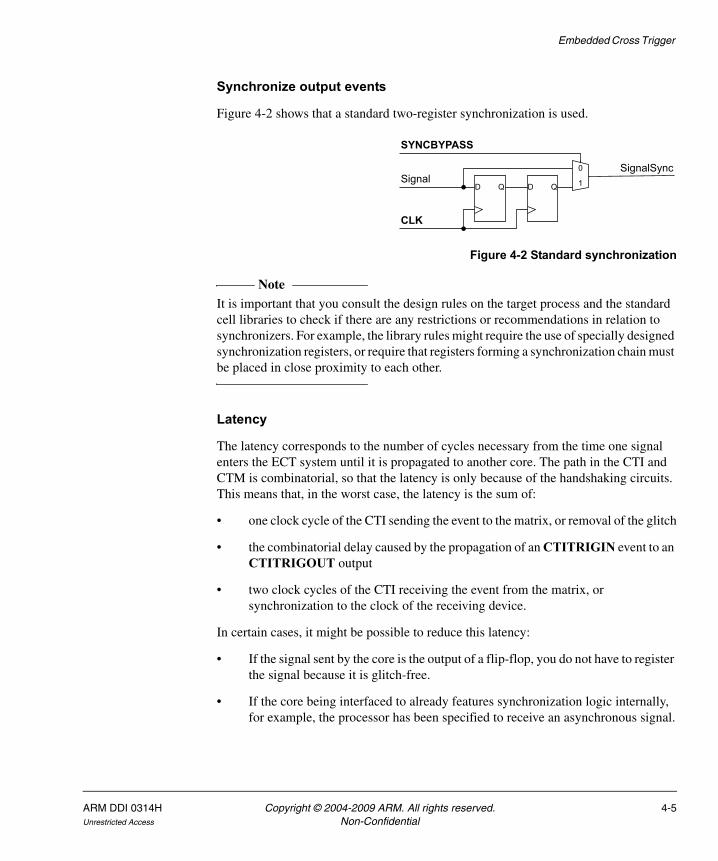
Embedded Cross Trigger
Synchronize output events
Figure 4-2 shows that a standard two-register synchronization is used.
Figure 4-2 Standard synchronization
Note It is important that you consult the design rules on the target process and the standard cell libraries to check if there are any restrictions or recommendations in relation to synchronizers. For example, the library rules might require the use of specially designed synchronization registers, or require that registers forming a synchronization chain must be placed in close proximity to each other.
Latency
The latency corresponds to the number of cycles necessary from the time one signal enters the ECT system until it is propagated to another core. The path in the CTI and CTM is combinatorial, so that the latency is only because of the handshaking circuits. This means that, in the worst case, the latency is the sum of:
• one clock cycle of the CTI sending the event to the matrix, or removal of the glitch
• the combinatorial delay caused by the propagation of an CTITRIGIN event to an CTITRIGOUT output
• two clock cycles of the CTI receiving the event from the matrix, or synchronization to the clock of the receiving device.
In certain cases, it might be possible to reduce this latency:
• If the signal sent by the core is the output of a flip-flop, you do not have to register the signal because it is glitch-free.
• If the core being interfaced to already features synchronization logic internally, for example, the processor has been specified to receive an asynchronous signal.
D Q
SYNCBYPASS
Signal
CLK
D Q
SignalSync0
1
ARM DDI 0314H Copyright © 2004-2009 ARM. All rights reserved. 4-5Unrestricted Access Non-Confidential
Embedded Cross Trigger
• If all the subsystems are synchronous, the TI bypass signals, TISBYPASSACK and TISBYPASSIN, can be activated. However, this path must respect the layout and synthesis timing constraints.
• If the CTM and CTI clocks are synchronous, the CI bypass signals, CISBYPASSACK and CISBYPASSIN can be activated.
Clock domains
In most systems the CTICLK is connected to the same clock as its local processor and the CTMCLK is connected to the fastest processor clock in the system so reducing the trigger latency and the requirement for clock enable ports.
If a CTI is going to be disabled while the processor enters a clock stopped mode, ARM recommends the following:
• The CTI turns off the event-to-channel mapping, so that unwanted events are not generated to the CTM.
• The channel-to-event mapping circuit is turned off or disabled for a few clock cycles after the clock is on.
• This version of the CTI must not be connected to clocks that might be removed, that is stopped. This version of the CTI must not be placed within a power domain that can be turned off. In these scenarios it is recommended that CTICLK is the same as CTMCLK.
When a processor clock is stopped, for example, waiting for an interrupt, the corresponding CTI can receive an event from the CTM. When the CTI clock is the same as the subsystem clock and the handshaking is not bypassed, the CTM keeps the signal active until an acknowledgement is received, which only occurs when the clock is started again. In this case, out-of-date events can happen on the core. This does not inhibit the channel being used by other processors.
However, if the CTI clock differs from the local processor clock, for example, it is gated differently, it is possible for the CTI to raise an event to the core using CTITRIGOUT, while the processor clock is off. If raising an event to the core must be avoided, the processor must disable its CTI before stopping the clock.
Linking CTIs and CTMs
Where the clock used on a CTI and a connected CTM, or CTM to CTM, or CTI to CTI, is asynchronous, then both the handshaking logic and synchronization registers must be left enabled, that is, CIHSBYPASS and CISBYPASS must be tied LOW.
4-6 Copyright © 2004-2009 ARM. All rights reserved. ARM DDI 0314HNon-Confidential Unrestricted Access
Embedded Cross Trigger
If both devices have synchronous clocks then synchronization can be bypassed, CISBYPASS tied HIGH, to reduce latency.
If both clocks are the same, that is, CTMCLK = CTICLK, and the channel is required to send multi-shot events, the handshaking can be bypassed by tying CIHSBYPASS HIGH.
ARM DDI 0314H Copyright © 2004-2009 ARM. All rights reserved. 4-7Unrestricted Access Non-Confidential
Embedded Cross Trigger
4.2 ECT programmers modelThe base addresses of the CTIs are not fixed, and can be different for any particular system implementation. However, the offset of any particular register from the base address is fixed. Each CTI has a 4KB programmers model. Each CTI must be programmed separately. All unused memory space is reserved.
The following applies to all registers:
• Reserved or unused bits of registers must be written as 0, and ignored on a read unless otherwise stated in the text.
• All register bits are reset to 0 unless otherwise stated in the text.
• All registers must be accessed as words and so are compatible with big-endian and little-endian systems.
Note The CTM does not have a programmers model itself because it is a link between two or more CTIs, or additional CTMs.
4-8 Copyright © 2004-2009 ARM. All rights reserved. ARM DDI 0314HNon-Confidential Unrestricted Access
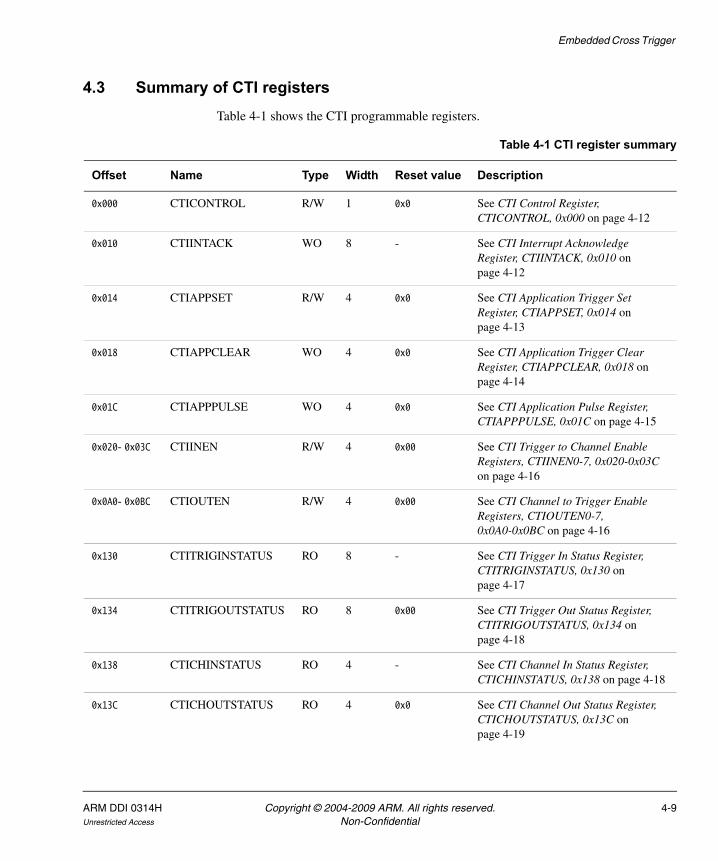
Embedded Cross Trigger
4.3 Summary of CTI registersTable 4-1 shows the CTI programmable registers.
Table 4-1 CTI register summary
Offset Name Type Width Reset value Description
0x000 CTICONTROL R/W 1 0x0 See CTI Control Register, CTICONTROL, 0x000 on page 4-12
0x010 CTIINTACK WO 8 - See CTI Interrupt Acknowledge Register, CTIINTACK, 0x010 on page 4-12
0x014 CTIAPPSET R/W 4 0x0 See CTI Application Trigger Set Register, CTIAPPSET, 0x014 on page 4-13
0x018 CTIAPPCLEAR WO 4 0x0 See CTI Application Trigger Clear Register, CTIAPPCLEAR, 0x018 on page 4-14
0x01C CTIAPPPULSE WO 4 0x0 See CTI Application Pulse Register, CTIAPPPULSE, 0x01C on page 4-15
0x020- 0x03C CTIINEN R/W 4 0x00 See CTI Trigger to Channel Enable Registers, CTIINEN0-7, 0x020-0x03C on page 4-16
0x0A0- 0x0BC CTIOUTEN R/W 4 0x00 See CTI Channel to Trigger Enable Registers, CTIOUTEN0-7, 0x0A0-0x0BC on page 4-16
0x130 CTITRIGINSTATUS RO 8 - See CTI Trigger In Status Register, CTITRIGINSTATUS, 0x130 on page 4-17
0x134 CTITRIGOUTSTATUS RO 8 0x00 See CTI Trigger Out Status Register, CTITRIGOUTSTATUS, 0x134 on page 4-18
0x138 CTICHINSTATUS RO 4 - See CTI Channel In Status Register, CTICHINSTATUS, 0x138 on page 4-18
0x13C CTICHOUTSTATUS RO 4 0x0 See CTI Channel Out Status Register, CTICHOUTSTATUS, 0x13C on page 4-19
ARM DDI 0314H Copyright © 2004-2009 ARM. All rights reserved. 4-9Unrestricted Access Non-Confidential
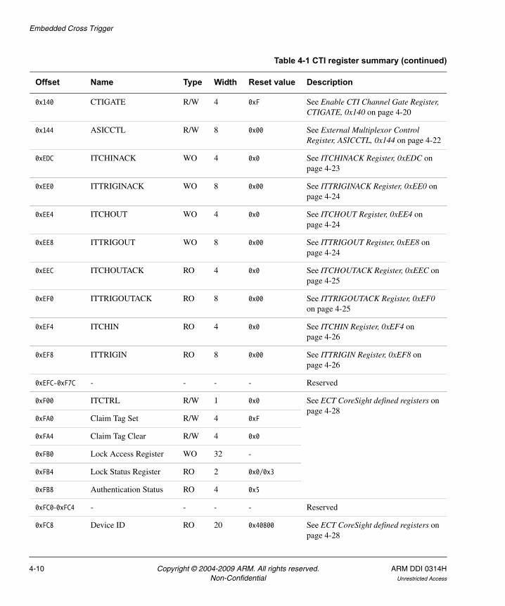
Embedded Cross Trigger
0x140 CTIGATE R/W 4 0xF See Enable CTI Channel Gate Register, CTIGATE, 0x140 on page 4-20
0x144 ASICCTL R/W 8 0x00 See External Multiplexor Control Register, ASICCTL, 0x144 on page 4-22
0xEDC ITCHINACK WO 4 0x0 See ITCHINACK Register, 0xEDC on page 4-23
0xEE0 ITTRIGINACK WO 8 0x00 See ITTRIGINACK Register, 0xEE0 on page 4-24
0xEE4 ITCHOUT WO 4 0x0 See ITCHOUT Register, 0xEE4 on page 4-24
0xEE8 ITTRIGOUT WO 8 0x00 See ITTRIGOUT Register, 0xEE8 on page 4-24
0xEEC ITCHOUTACK RO 4 0x0 See ITCHOUTACK Register, 0xEEC on page 4-25
0xEF0 ITTRIGOUTACK RO 8 0x00 See ITTRIGOUTACK Register, 0xEF0 on page 4-25
0xEF4 ITCHIN RO 4 0x0 See ITCHIN Register, 0xEF4 on page 4-26
0xEF8 ITTRIGIN RO 8 0x00 See ITTRIGIN Register, 0xEF8 on page 4-26
0xEFC-0xF7C - - - - Reserved
0xF00 ITCTRL R/W 1 0x0 See ECT CoreSight defined registers on page 4-28
0xFA0 Claim Tag Set R/W 4 0xF
0xFA4 Claim Tag Clear R/W 4 0x0
0xFB0 Lock Access Register WO 32 -
0xFB4 Lock Status Register RO 2 0x0/0x3
0xFB8 Authentication Status RO 4 0x5
0xFC0-0xFC4 - - - - Reserved
0xFC8 Device ID RO 20 0x40800 See ECT CoreSight defined registers on page 4-28
Table 4-1 CTI register summary (continued)
Offset Name Type Width Reset value Description
4-10 Copyright © 2004-2009 ARM. All rights reserved. ARM DDI 0314HNon-Confidential Unrestricted Access
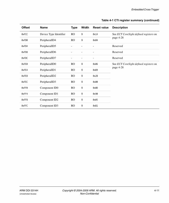
Embedded Cross Trigger
0xFCC Device Type Identifier RO 8 0x14 See ECT CoreSight defined registers on page 4-28
0xFD0 PeripheralID4 RO 8 0x04
0xFD4 PeripheralID5 - - - Reserved
0xFD8 PeripheralID6 - - - Reserved
0xFDC PeripheralID7 - - - Reserved
0xFE0 PeripheralID0 RO 8 0x06 See ECT CoreSight defined registers on page 4-28
0xFE4 PeripheralID1 RO 8 0xB9
0xFE8 PeripheralID2 RO 8 0x2B
0xFEC PeripheralID3 RO 8 0x00
0xFF0 Component ID0 RO 8 0x0D
0xFF4 Component ID1 RO 8 0x90
0xFF8 Component ID2 RO 8 0x05
0xFFC Component ID3 RO 8 0xB1
Table 4-1 CTI register summary (continued)
Offset Name Type Width Reset value Description
ARM DDI 0314H Copyright © 2004-2009 ARM. All rights reserved. 4-11Unrestricted Access Non-Confidential
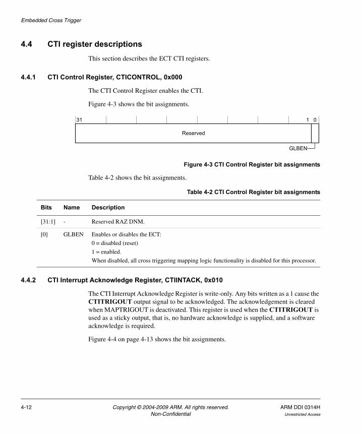
Embedded Cross Trigger
4.4 CTI register descriptionsThis section describes the ECT CTI registers.
4.4.1 CTI Control Register, CTICONTROL, 0x000
The CTI Control Register enables the CTI.
Figure 4-3 shows the bit assignments.
Figure 4-3 CTI Control Register bit assignments
Table 4-2 shows the bit assignments.
4.4.2 CTI Interrupt Acknowledge Register, CTIINTACK, 0x010
The CTI Interrupt Acknowledge Register is write-only. Any bits written as a 1 cause the CTITRIGOUT output signal to be acknowledged. The acknowledgement is cleared when MAPTRIGOUT is deactivated. This register is used when the CTITRIGOUT is used as a sticky output, that is, no hardware acknowledge is supplied, and a software acknowledge is required.
Figure 4-4 on page 4-13 shows the bit assignments.
GLBEN
Reserved
31 1 0
Table 4-2 CTI Control Register bit assignments
Bits Name Description
[31:1] - Reserved RAZ DNM.
[0] GLBEN Enables or disables the ECT:
0 = disabled (reset)
1 = enabled.
When disabled, all cross triggering mapping logic functionality is disabled for this processor.
4-12 Copyright © 2004-2009 ARM. All rights reserved. ARM DDI 0314HNon-Confidential Unrestricted Access
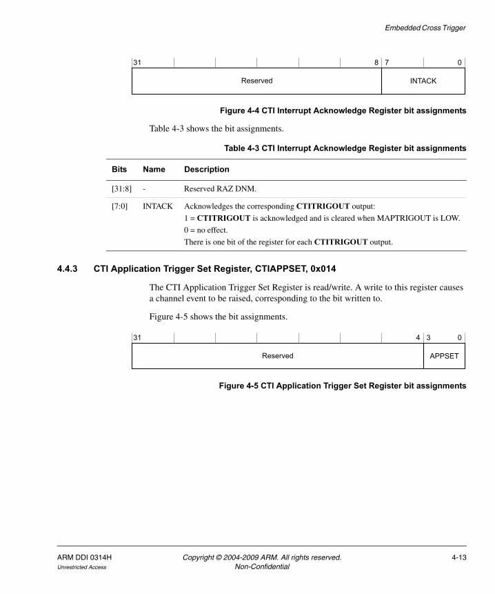
Embedded Cross Trigger
Figure 4-4 CTI Interrupt Acknowledge Register bit assignments
Table 4-3 shows the bit assignments.
4.4.3 CTI Application Trigger Set Register, CTIAPPSET, 0x014
The CTI Application Trigger Set Register is read/write. A write to this register causes a channel event to be raised, corresponding to the bit written to.
Figure 4-5 shows the bit assignments.
Figure 4-5 CTI Application Trigger Set Register bit assignments
INTACKReserved
31 8 07
Table 4-3 CTI Interrupt Acknowledge Register bit assignments
Bits Name Description
[31:8] - Reserved RAZ DNM.
[7:0] INTACK Acknowledges the corresponding CTITRIGOUT output:
1 = CTITRIGOUT is acknowledged and is cleared when MAPTRIGOUT is LOW.
0 = no effect.
There is one bit of the register for each CTITRIGOUT output.
APPSETReserved
31 4 03
ARM DDI 0314H Copyright © 2004-2009 ARM. All rights reserved. 4-13Unrestricted Access Non-Confidential
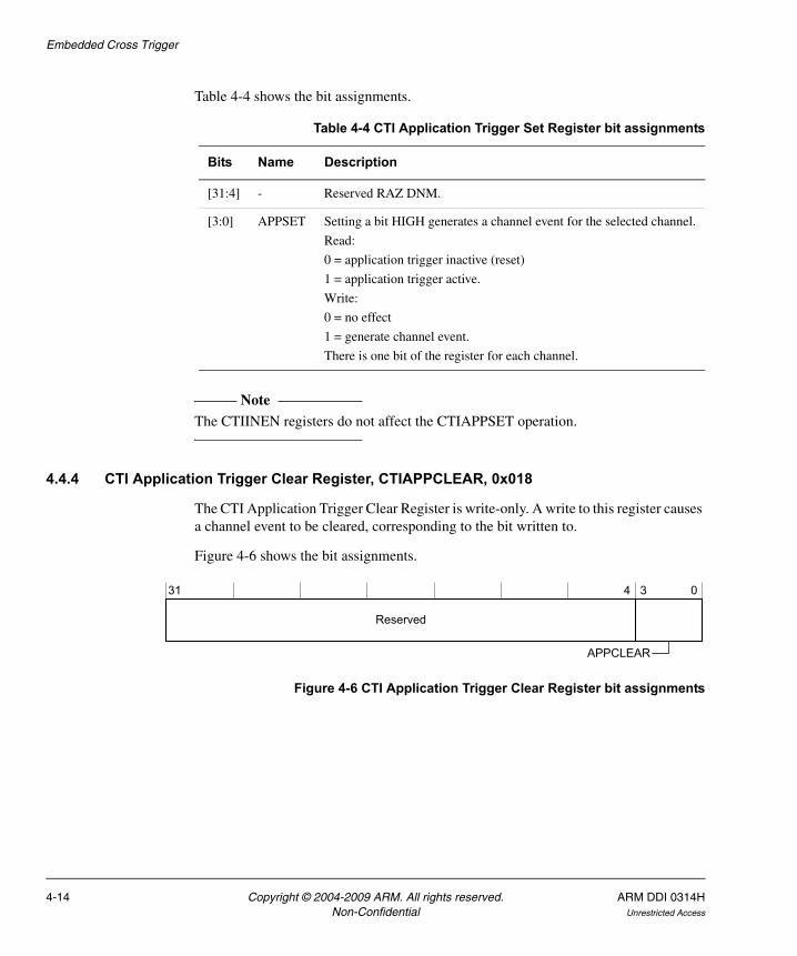
Embedded Cross Trigger
Table 4-4 shows the bit assignments.
Note The CTIINEN registers do not affect the CTIAPPSET operation.
4.4.4 CTI Application Trigger Clear Register, CTIAPPCLEAR, 0x018
The CTI Application Trigger Clear Register is write-only. A write to this register causes a channel event to be cleared, corresponding to the bit written to.
Figure 4-6 shows the bit assignments.
Figure 4-6 CTI Application Trigger Clear Register bit assignments
Table 4-4 CTI Application Trigger Set Register bit assignments
Bits Name Description
[31:4] - Reserved RAZ DNM.
[3:0] APPSET Setting a bit HIGH generates a channel event for the selected channel.
Read:
0 = application trigger inactive (reset)
1 = application trigger active.
Write:
0 = no effect
1 = generate channel event.
There is one bit of the register for each channel.
Reserved
31 4 03
APPCLEAR
4-14 Copyright © 2004-2009 ARM. All rights reserved. ARM DDI 0314HNon-Confidential Unrestricted Access
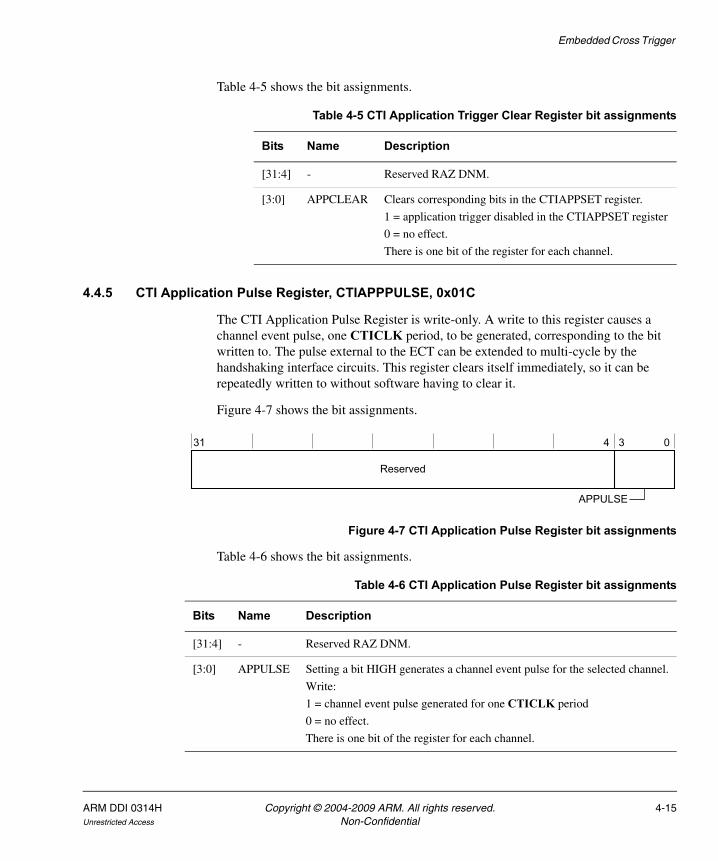
Embedded Cross Trigger
Table 4-5 shows the bit assignments.
4.4.5 CTI Application Pulse Register, CTIAPPPULSE, 0x01C
The CTI Application Pulse Register is write-only. A write to this register causes a channel event pulse, one CTICLK period, to be generated, corresponding to the bit written to. The pulse external to the ECT can be extended to multi-cycle by the handshaking interface circuits. This register clears itself immediately, so it can be repeatedly written to without software having to clear it.
Figure 4-7 shows the bit assignments.
Figure 4-7 CTI Application Pulse Register bit assignments
Table 4-6 shows the bit assignments.
Table 4-5 CTI Application Trigger Clear Register bit assignments
Bits Name Description
[31:4] - Reserved RAZ DNM.
[3:0] APPCLEAR Clears corresponding bits in the CTIAPPSET register.
1 = application trigger disabled in the CTIAPPSET register
0 = no effect.
There is one bit of the register for each channel.
Reserved
31 4 03
APPULSE
Table 4-6 CTI Application Pulse Register bit assignments
Bits Name Description
[31:4] - Reserved RAZ DNM.
[3:0] APPULSE Setting a bit HIGH generates a channel event pulse for the selected channel.
Write:
1 = channel event pulse generated for one CTICLK period
0 = no effect.
There is one bit of the register for each channel.
ARM DDI 0314H Copyright © 2004-2009 ARM. All rights reserved. 4-15Unrestricted Access Non-Confidential
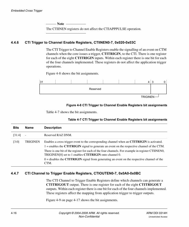
Embedded Cross Trigger
Note The CTIINEN registers do not affect the CTIAPPPULSE operation.
4.4.6 CTI Trigger to Channel Enable Registers, CTIINEN0-7, 0x020-0x03C
The CTI Trigger to Channel Enable Registers enable the signalling of an event on CTM channels when the core issues a trigger, CTITRIGIN, to the CTI. There is one register for each of the eight CTITRIGIN inputs. Within each register there is one bit for each of the four channels implemented. These registers do not affect the application trigger operations.
Figure 4-8 shows the bit assignments.
Figure 4-8 CTI Trigger to Channel Enable Registers bit assignments
Table 4-7 shows the bit assignments.
4.4.7 CTI Channel to Trigger Enable Registers, CTIOUTEN0-7, 0x0A0-0x0BC
The CTI Channel to Trigger Enable Registers define which channels can generate a CTITRIGOUT output. There is one register for each of the eight CTITRIGOUT outputs. Within each register there is one bit for each of the four channels implemented. These registers affect the mapping from application trigger to trigger outputs.
Figure 4-9 on page 4-17 shows the bit assignments.
Reserved
31 4 03
TRIGINEN
Table 4-7 CTI Trigger to Channel Enable Registers bit assignments
Bits Name Description
[31:4] - Reserved RAZ DNM.
[3:0] TRIGINEN Enables a cross trigger event to the corresponding channel when an CTITRIGIN is activated.
1 = enables the CTITRIGIN signal to generate an event on the respective channel of the CTM.
There is one bit of the register for each of the four channels. For example in register CTIINEN0, TRIGINEN[0] set to 1 enables CTITRIGIN onto channel 0.
0 = disables the CTITRIGIN signal from generating an event on the respective channel of the CTM.
4-16 Copyright © 2004-2009 ARM. All rights reserved. ARM DDI 0314HNon-Confidential Unrestricted Access
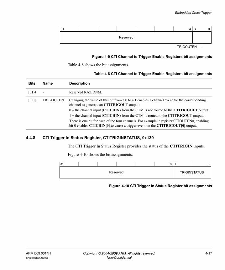
Embedded Cross Trigger
Figure 4-9 CTI Channel to Trigger Enable Registers bit assignments
Table 4-8 shows the bit assignments.
4.4.8 CTI Trigger In Status Register, CTITRIGINSTATUS, 0x130
The CTI Trigger In Status Register provides the status of the CTITRIGIN inputs.
Figure 4-10 shows the bit assignments.
Figure 4-10 CTI Trigger In Status Register bit assignments
Reserved
31 4 03
TRIGOUTEN
Table 4-8 CTI Channel to Trigger Enable Registers bit assignments
Bits Name Description
[31:4] - Reserved RAZ DNM.
[3:0] TRIGOUTEN Changing the value of this bit from a 0 to a 1 enables a channel event for the corresponding channel to generate an CTITRIGOUT output:
0 = the channel input (CTICHIN) from the CTM is not routed to the CTITRIGOUT output
1 = the channel input (CTICHIN) from the CTM is routed to the CTITRIGOUT output.
There is one bit for each of the four channels. For example in register CTIOUTEN0, enabling bit 0 enables CTICHIN[0] to cause a trigger event on the CTITRIGOUT[0] output.
TRIGINSTATUSReserved
31 8 07
ARM DDI 0314H Copyright © 2004-2009 ARM. All rights reserved. 4-17Unrestricted Access Non-Confidential
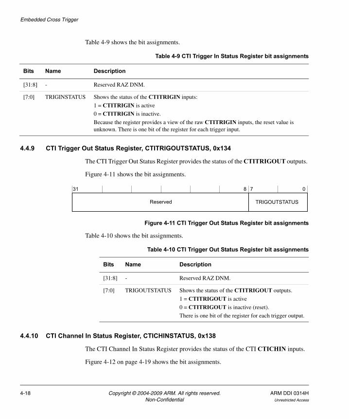
Embedded Cross Trigger
Table 4-9 shows the bit assignments.
4.4.9 CTI Trigger Out Status Register, CTITRIGOUTSTATUS, 0x134
The CTI Trigger Out Status Register provides the status of the CTITRIGOUT outputs.
Figure 4-11 shows the bit assignments.
Figure 4-11 CTI Trigger Out Status Register bit assignments
Table 4-10 shows the bit assignments.
4.4.10 CTI Channel In Status Register, CTICHINSTATUS, 0x138
The CTI Channel In Status Register provides the status of the CTI CTICHIN inputs.
Figure 4-12 on page 4-19 shows the bit assignments.
Table 4-9 CTI Trigger In Status Register bit assignments
Bits Name Description
[31:8] - Reserved RAZ DNM.
[7:0] TRIGINSTATUS Shows the status of the CTITRIGIN inputs:
1 = CTITRIGIN is active
0 = CTITRIGIN is inactive.
Because the register provides a view of the raw CTITRIGIN inputs, the reset value is unknown. There is one bit of the register for each trigger input.
TRIGOUTSTATUSReserved
31 8 07
Table 4-10 CTI Trigger Out Status Register bit assignments
Bits Name Description
[31:8] - Reserved RAZ DNM.
[7:0] TRIGOUTSTATUS Shows the status of the CTITRIGOUT outputs.
1 = CTITRIGOUT is active
0 = CTITRIGOUT is inactive (reset).
There is one bit of the register for each trigger output.
4-18 Copyright © 2004-2009 ARM. All rights reserved. ARM DDI 0314HNon-Confidential Unrestricted Access
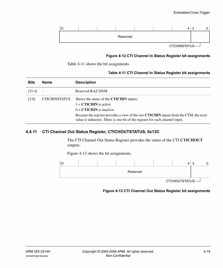
Embedded Cross Trigger
Figure 4-12 CTI Channel In Status Register bit assignments
Table 4-11 shows the bit assignments.
4.4.11 CTI Channel Out Status Register, CTICHOUTSTATUS, 0x13C
The CTI Channel Out Status Register provides the status of the CTI CTICHOUT outputs.
Figure 4-13 shows the bit assignments.
Figure 4-13 CTI Channel Out Status Register bit assignments
Reserved
31 4 03
CTCHINSTATUS
Table 4-11 CTI Channel In Status Register bit assignments
Bits Name Description
[31:4] - Reserved RAZ DNM.
[3:0] CTICHINSTATUS Shows the status of the CTICHIN inputs:
1 = CTICHIN is active
0 = CTICHIN is inactive.
Because the register provides a view of the raw CTICHIN inputs from the CTM, the reset value is unknown. There is one bit of the register for each channel input.
Reserved
31 4 03
CTCHOUTSTATUS
ARM DDI 0314H Copyright © 2004-2009 ARM. All rights reserved. 4-19Unrestricted Access Non-Confidential
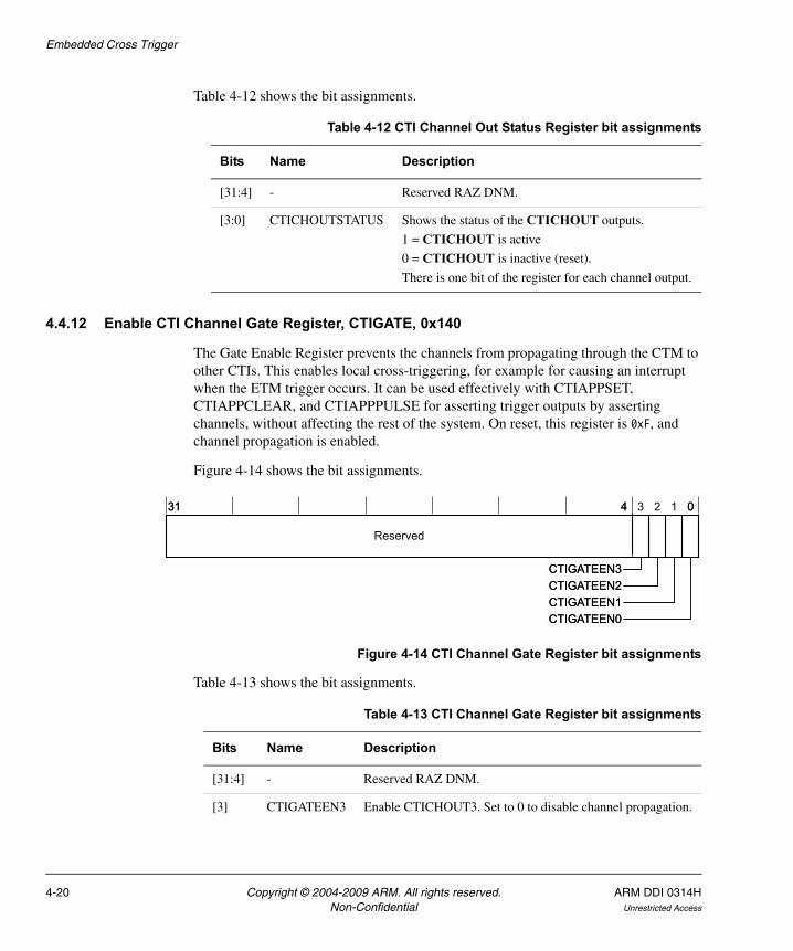
Embedded Cross Trigger
Table 4-12 shows the bit assignments.
4.4.12 Enable CTI Channel Gate Register, CTIGATE, 0x140
The Gate Enable Register prevents the channels from propagating through the CTM to other CTIs. This enables local cross-triggering, for example for causing an interrupt when the ETM trigger occurs. It can be used effectively with CTIAPPSET, CTIAPPCLEAR, and CTIAPPPULSE for asserting trigger outputs by asserting channels, without affecting the rest of the system. On reset, this register is 0xF, and channel propagation is enabled.
Figure 4-14 shows the bit assignments.
Figure 4-14 CTI Channel Gate Register bit assignments
Table 4-13 shows the bit assignments.
Table 4-12 CTI Channel Out Status Register bit assignments
Bits Name Description
[31:4] - Reserved RAZ DNM.
[3:0] CTICHOUTSTATUS Shows the status of the CTICHOUT outputs.
1 = CTICHOUT is active
0 = CTICHOUT is inactive (reset).
There is one bit of the register for each channel output.
Reserved
31 4 03
CTIGATEEN3
12
CTIGATEEN2CTIGATEEN1CTIGATEEN0
Reserved
31 4 0
CTIGATEEN3CTIGATEEN2CTIGATEEN1CTIGATEEN0
Table 4-13 CTI Channel Gate Register bit assignments
Bits Name Description
[31:4] - Reserved RAZ DNM.
[3] CTIGATEEN3 Enable CTICHOUT3. Set to 0 to disable channel propagation.
4-20 Copyright © 2004-2009 ARM. All rights reserved. ARM DDI 0314HNon-Confidential Unrestricted Access

Embedded Cross Trigger
Figure 4-15 shows channel gates used with the CTI.
Figure 4-15 Channel gate used with the CTI
[2] CTIGATEEN2 Enable CTICHOUT2. Set to 0 to disable channel propagation.
[1] CTIGATEEN1 Enable CTICHOUT1. Set to 0 to disable channel propagation.
[0] CTIGATEEN0 Enable CTICHOUT0. Set to 0 to disable channel propagation.
Table 4-13 CTI Channel Gate Register bit assignments (continued)
Bits Name Description
Cross-trigger interface
Application set/ clear/
pulse registers
[3:0]
Gate enable register
[3:0]
CTM
Trigger channel to debug channel mapping
CTITRIGOUT[7:0]
CTITRIGIN[7:0]
&&&&
CTICHIN
CTMCHOUT
CTICHOUT
Gateenable
APB I/F
CoreWrapper -
Trigger interface
CTMCHIN
APB I/F
ARM DDI 0314H Copyright © 2004-2009 ARM. All rights reserved. 4-21Unrestricted Access Non-Confidential
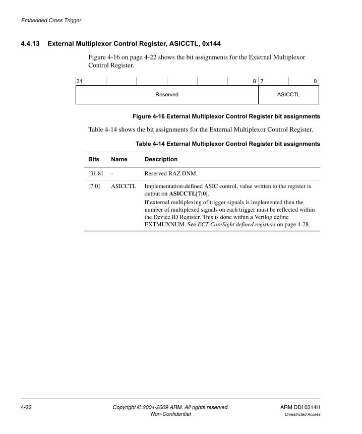
Embedded Cross Trigger
4.4.13 External Multiplexor Control Register, ASICCTL, 0x144
Figure 4-16 on page 4-22 shows the bit assignments for the External Multiplexor Control Register.
Figure 4-16 External Multiplexor Control Register bit assignments
Table 4-14 shows the bit assignments for the External Multiplexor Control Register.
ASICCTLReserved
31 8 07
Table 4-14 External Multiplexor Control Register bit assignments
Bits Name Description
[31:8] - Reserved RAZ DNM.
[7:0] ASICCTL Implementation-defined ASIC control, value written to the register is output on ASICCTL[7:0].If external multiplexing of trigger signals is implemented then the number of multiplexed signals on each trigger must be reflected within the Device ID Register. This is done within a Verilog define EXTMUXNUM. See ECT CoreSight defined registers on page 4-28.
4-22 Copyright © 2004-2009 ARM. All rights reserved. ARM DDI 0314HNon-Confidential Unrestricted Access

Embedded Cross Trigger
4.5 ECT Integration Test RegistersIntegration Test Registers are provided to simplify the process of verifying the integration of the ECT with other devices in a CoreSight system. These registers enable direct control of outputs and the ability to read the value of inputs. You must only use these registers when the Integration Mode Control Register (0xF00) bit [0] is set to 1.
For details of how to use these signals, see the CoreSight Components Implementation Guide and the applicable Integration Manual.
This section describes the following registers:
• ITCHINACK Register, 0xEDC
• ITTRIGINACK Register, 0xEE0 on page 4-24
• ITCHOUT Register, 0xEE4 on page 4-24
• ITTRIGOUT Register, 0xEE8 on page 4-24
• ITCHOUTACK Register, 0xEEC on page 4-25
• ITTRIGOUTACK Register, 0xEF0 on page 4-25
• ITCHIN Register, 0xEF4 on page 4-26
• ITTRIGIN Register, 0xEF8 on page 4-26.
4.5.1 ITCHINACK Register, 0xEDC
This register is a write-only register. Figure 4-17 shows the bit assignments.
Figure 4-17 ITCINACK Register bit assignments
Table 4-15 shows the bit assignments.
31 0
CTCHINACK
Reserved
34
Table 4-15 ITCHINACK Register bit assignments
Bits Name Description
[31:4] - Reserved
[3:0] CTCHINACK Set the value of the CTCHINACK outputs
ARM DDI 0314H Copyright © 2004-2009 ARM. All rights reserved. 4-23Unrestricted Access Non-Confidential
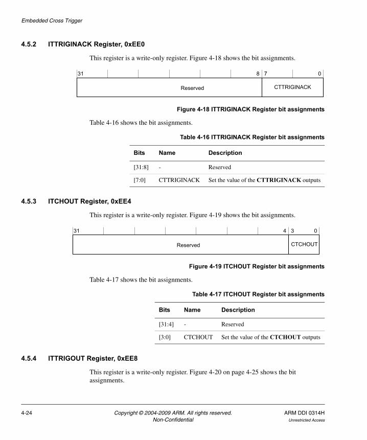
Embedded Cross Trigger
4.5.2 ITTRIGINACK Register, 0xEE0
This register is a write-only register. Figure 4-18 shows the bit assignments.
Figure 4-18 ITTRIGINACK Register bit assignments
Table 4-16 shows the bit assignments.
4.5.3 ITCHOUT Register, 0xEE4
This register is a write-only register. Figure 4-19 shows the bit assignments.
Figure 4-19 ITCHOUT Register bit assignments
Table 4-17 shows the bit assignments.
4.5.4 ITTRIGOUT Register, 0xEE8
This register is a write-only register. Figure 4-20 on page 4-25 shows the bit assignments.
31 0
CTTRIGINACKReserved
78
Table 4-16 ITTRIGINACK Register bit assignments
Bits Name Description
[31:8] - Reserved
[7:0] CTTRIGINACK Set the value of the CTTRIGINACK outputs
31 0
CTCHOUTReserved
34
Table 4-17 ITCHOUT Register bit assignments
Bits Name Description
[31:4] - Reserved
[3:0] CTCHOUT Set the value of the CTCHOUT outputs
4-24 Copyright © 2004-2009 ARM. All rights reserved. ARM DDI 0314HNon-Confidential Unrestricted Access
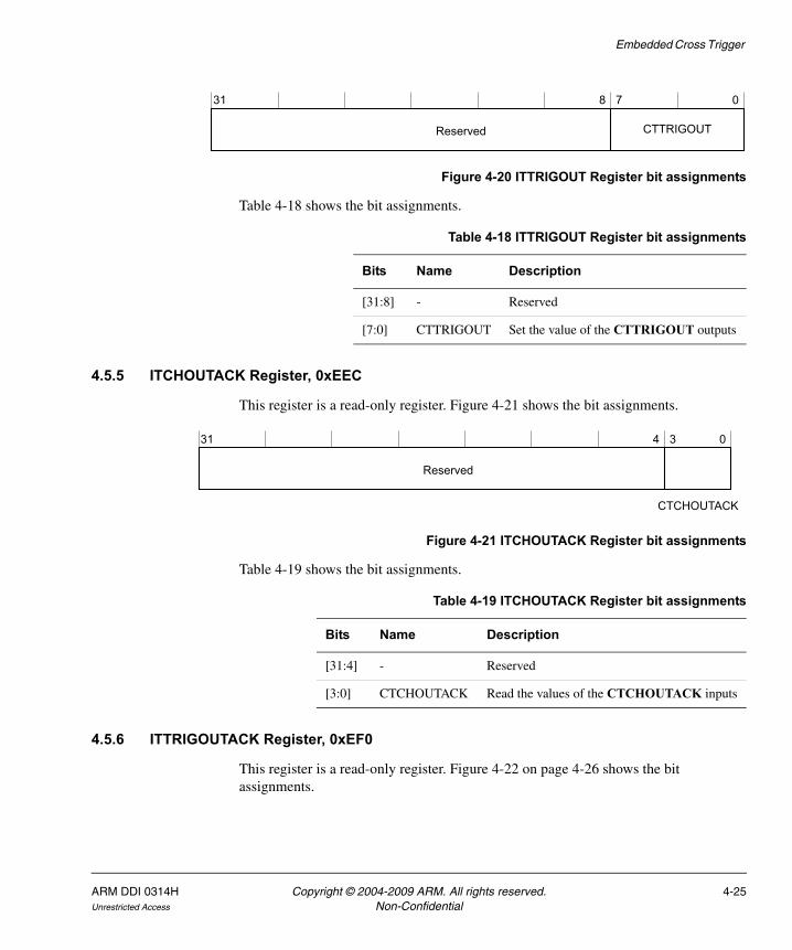
Embedded Cross Trigger
Figure 4-20 ITTRIGOUT Register bit assignments
Table 4-18 shows the bit assignments.
4.5.5 ITCHOUTACK Register, 0xEEC
This register is a read-only register. Figure 4-21 shows the bit assignments.
Figure 4-21 ITCHOUTACK Register bit assignments
Table 4-19 shows the bit assignments.
4.5.6 ITTRIGOUTACK Register, 0xEF0
This register is a read-only register. Figure 4-22 on page 4-26 shows the bit assignments.
31 0
CTTRIGOUTReserved
78
Table 4-18 ITTRIGOUT Register bit assignments
Bits Name Description
[31:8] - Reserved
[7:0] CTTRIGOUT Set the value of the CTTRIGOUT outputs
31 0
CTCHOUTACK
Reserved
34
Table 4-19 ITCHOUTACK Register bit assignments
Bits Name Description
[31:4] - Reserved
[3:0] CTCHOUTACK Read the values of the CTCHOUTACK inputs
ARM DDI 0314H Copyright © 2004-2009 ARM. All rights reserved. 4-25Unrestricted Access Non-Confidential
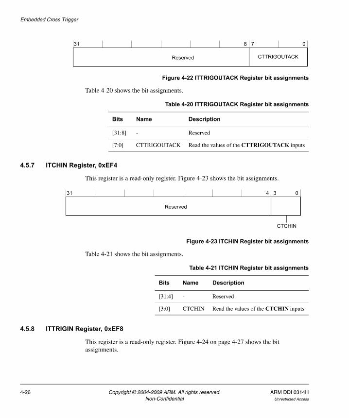
Embedded Cross Trigger
Figure 4-22 ITTRIGOUTACK Register bit assignments
Table 4-20 shows the bit assignments.
4.5.7 ITCHIN Register, 0xEF4
This register is a read-only register. Figure 4-23 shows the bit assignments.
Figure 4-23 ITCHIN Register bit assignments
Table 4-21 shows the bit assignments.
4.5.8 ITTRIGIN Register, 0xEF8
This register is a read-only register. Figure 4-24 on page 4-27 shows the bit assignments.
31 0
CTTRIGOUTACKReserved
78
Table 4-20 ITTRIGOUTACK Register bit assignments
Bits Name Description
[31:8] - Reserved
[7:0] CTTRIGOUTACK Read the values of the CTTRIGOUTACK inputs
31 0
CTCHIN
Reserved
34
Table 4-21 ITCHIN Register bit assignments
Bits Name Description
[31:4] - Reserved
[3:0] CTCHIN Read the values of the CTCHIN inputs
4-26 Copyright © 2004-2009 ARM. All rights reserved. ARM DDI 0314HNon-Confidential Unrestricted Access
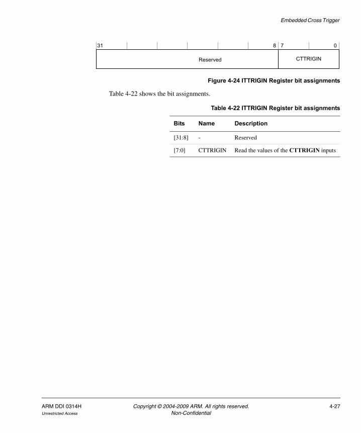
Embedded Cross Trigger
Figure 4-24 ITTRIGIN Register bit assignments
Table 4-22 shows the bit assignments.
31 0
CTTRIGINReserved
78
Table 4-22 ITTRIGIN Register bit assignments
Bits Name Description
[31:8] - Reserved
[7:0] CTTRIGIN Read the values of the CTTRIGIN inputs
ARM DDI 0314H Copyright © 2004-2009 ARM. All rights reserved. 4-27Unrestricted Access Non-Confidential

Embedded Cross Trigger
4.6 ECT CoreSight defined registersSee the CoreSight Architecture Specification for the definitions of these registers.
The information given here is specific to the ECT:
Claim tags, 0xFA0 and 0xFA4
The CTI implements a four-bit claim tag. The use of bits [3:0] is software defined.
Lock access mechanism, 0xFB0 and 0xFB4
The CTI implements two memory maps controlled through PADDRDBG31. When PADDRDBG31 is HIGH, the Lock Status Register reads as 0x0 indicating that no lock exists. When PADDRDBG31 is LOW, the Lock Status Register reads as 0x3 from reset. This indicates a 32-bit lock access mechanism is present and is locked.
Authentication Status Register, 0xFB8
Reports the required security level. Table 4-23 shows the authentication values.
Table 4-23 Authentication values for ECT
Bits Value Description
[31:4] 0x0000000 Reserved
[3] - Current value of noninvasive debug enable signals
[2] 1'b1 Non-invasive debug controlled
[1] - Current value of invasive debug enable signals
[0] 1'b1 Invasive debug controlled
4-28 Copyright © 2004-2009 ARM. All rights reserved. ARM DDI 0314HNon-Confidential Unrestricted Access
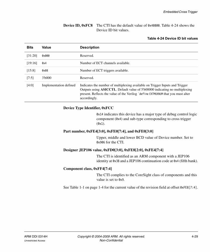
Embedded Cross Trigger
Device ID, 0xFC8 The CTI has the default value of 0x40800. Table 4-24 shows the Device ID bit values.
Device Type Identifier, 0xFCC
0x14 indicates this device has a major type of debug control logic component (0x4) and sub-type corresponding to cross trigger (0x1).
Part number, 0xFE4[3:0], 0xFE0[7:4], and 0xFE0[3:0]
Upper, middle and lower BCD value of Device number. Set to 0x906 for the CTI.
Designer JEP106 value, 0xFD0[3:0], 0xFE8[2:0], 0xFE4[7:4]
The CTI is identified as an ARM component with a JEP106 identity at 0x3B and a JEP106 continuation code at 0x4 (fifth bank).
Component class, 0xFF4[7:4]
The CTI complies to the CoreSight class of components and this value is set to 0x9.
See Table 1-1 on page 1-4 for the current value of the revision field at offset 0xFE8[7:4].
Table 4-24 Device ID bit values
Bits Value Description
[31:20] 0x000 Reserved.
[19:16] 0x4 Number of ECT channels available.
[15:8] 0x08 Number of ECT triggers available.
[7:5] 3'b000 Reserved.
[4:0] Implementation defined Indicates the number of multiplexing available on Trigger Inputs and Trigger Outputs using ASICCTL. Default value of 5'b00000 indicating no multiplexing present. Reflects the value of the Verilog `define EXTMUXNUM that you must alter accordingly.
ARM DDI 0314H Copyright © 2004-2009 ARM. All rights reserved. 4-29Unrestricted Access Non-Confidential
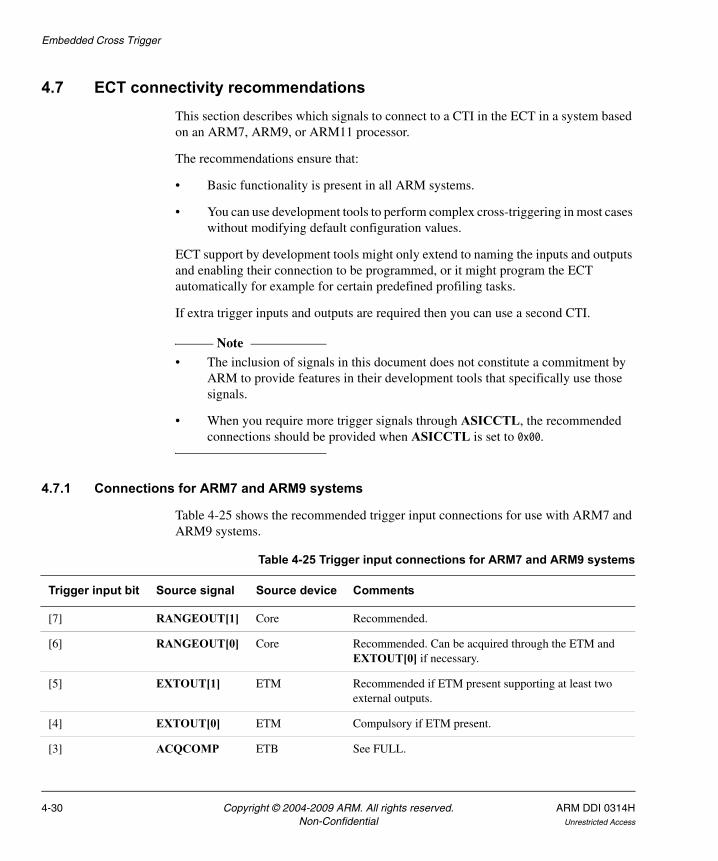
Embedded Cross Trigger
4.7 ECT connectivity recommendationsThis section describes which signals to connect to a CTI in the ECT in a system based on an ARM7, ARM9, or ARM11 processor.
The recommendations ensure that:
• Basic functionality is present in all ARM systems.
• You can use development tools to perform complex cross-triggering in most cases without modifying default configuration values.
ECT support by development tools might only extend to naming the inputs and outputs and enabling their connection to be programmed, or it might program the ECT automatically for example for certain predefined profiling tasks.
If extra trigger inputs and outputs are required then you can use a second CTI.
Note • The inclusion of signals in this document does not constitute a commitment by
ARM to provide features in their development tools that specifically use those signals.
• When you require more trigger signals through ASICCTL, the recommended connections should be provided when ASICCTL is set to 0x00.
4.7.1 Connections for ARM7 and ARM9 systems
Table 4-25 shows the recommended trigger input connections for use with ARM7 and ARM9 systems.
Table 4-25 Trigger input connections for ARM7 and ARM9 systems
Trigger input bit Source signal Source device Comments
[7] RANGEOUT[1] Core Recommended.
[6] RANGEOUT[0] Core Recommended. Can be acquired through the ETM and EXTOUT[0] if necessary.
[5] EXTOUT[1] ETM Recommended if ETM present supporting at least two external outputs.
[4] EXTOUT[0] ETM Compulsory if ETM present.
[3] ACQCOMP ETB See FULL.
4-30 Copyright © 2004-2009 ARM. All rights reserved. ARM DDI 0314HNon-Confidential Unrestricted Access

Embedded Cross Trigger
Inputs not connected as shown in Table 4-25 on page 4-30 can be used for user-defined functions.
Table 4-26 shows the recommended trigger output connections for ARM7 and ARM9 systems.
Outputs not connected as shown in Table 4-26 can be used for user-defined functions.
[2] FULL ETB Recommended if an ETB is present. If a single ETB is shared between multiple cores, only connect to the CTI of one of the cores.
[1] User defined - -
[0] DBGACK Core Compulsory.
Table 4-25 Trigger input connections for ARM7 and ARM9 systems (continued)
Trigger input bit Source signal Source device Comments
Table 4-26 Trigger output connections for ARM7 and ARM9 systems
Trigger output bit Destination signal Destination device Comments
[7] DBGEXT[1]/EXTERN1 Core Recommended.
[6] DBGEXT[0]/ EXTERN0 Core Recommended.
[5] EXTIN[1] ETM Recommended if ETM present.
[4] EXTIN[0] ETM Compulsory if ETM present.
[3] VICINTSOURCE[y] VIC Recommended if the Vectored Interrupt Controller (VIC) is present. Any interrupt can be used.
[2] VICINTSOURCE[x] VIC Compulsory if the VIC is present. Any interrupt can be used.
!nIRQ Core Compulsory if the VIC is not present. The output must be negated and connected to the core nIRQ input, ANDed with other signals using this input.
[1] User-defined - -
[0] DBGRQ/EDBGRQ Core Compulsory.
ARM DDI 0314H Copyright © 2004-2009 ARM. All rights reserved. 4-31Unrestricted Access Non-Confidential
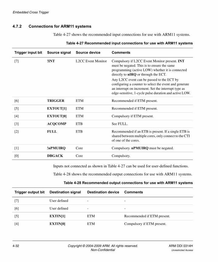
Embedded Cross Trigger
4.7.2 Connections for ARM11 systems
Table 4-27 shows the recommended input connections for use with ARM11 systems.
Inputs not connected as shown in Table 4-27 can be used for user-defined functions.
Table 4-28 shows the recommended output connections for use with ARM11 systems.
Table 4-27 Recommended input connections for use with ARM11 systems
Trigger input bit Source signal Source device Comments
[7] !INT L2CC Event Monitor Compulsory if L2CC Event Monitor present. INT must be negated. This is to ensure the same programming (active LOW) whether it is connected directly to nIRQ or through the ECT.
Any L2CC event can be passed to the ECT by configuring a counter to select the event and generate an interrupt on increment. Set the interrupt type as edge-sensitive, 1-cycle pulse duration and active LOW.
[6] TRIGGER ETM Recommended if ETM present.
[5] EXTOUT[1] ETM Recommended if ETM present.
[4] EXTOUT[0] ETM Compulsory if ETM present.
[3] ACQCOMP ETB See FULL.
[2] FULL ETB Recommended if an ETB is present. If a single ETB is shared between multiple cores, only connect to the CTI of one of the cores.
[1] !nPMUIRQ Core Compulsory. nPMUIRQ must be negated.
[0] DBGACK Core Compulsory.
Table 4-28 Recommended output connections for use with ARM11 systems
Trigger output bit Destination signal Destination device Comments
[7] User defined - -
[6] User defined - -
[5] EXTIN[1] ETM Recommended if ETM present.
[4] EXTIN[0] ETM Compulsory if ETM present.
4-32 Copyright © 2004-2009 ARM. All rights reserved. ARM DDI 0314HNon-Confidential Unrestricted Access
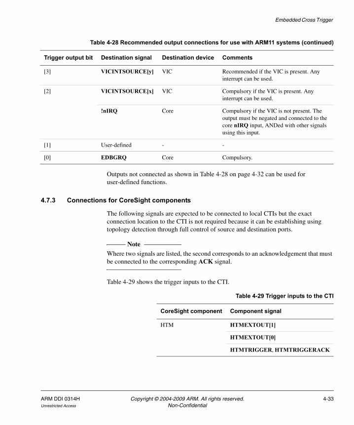
Embedded Cross Trigger
Outputs not connected as shown in Table 4-28 on page 4-32 can be used for user-defined functions.
4.7.3 Connections for CoreSight components
The following signals are expected to be connected to local CTIs but the exact connection location to the CTI is not required because it can be establishing using topology detection through full control of source and destination ports.
Note Where two signals are listed, the second corresponds to an acknowledgement that must be connected to the corresponding ACK signal.
Table 4-29 shows the trigger inputs to the CTI.
[3] VICINTSOURCE[y] VIC Recommended if the VIC is present. Any interrupt can be used.
[2] VICINTSOURCE[x] VIC Compulsory if the VIC is present. Any interrupt can be used.
!nIRQ Core Compulsory if the VIC is not present. The output must be negated and connected to the core nIRQ input, ANDed with other signals using this input.
[1] User-defined - -
[0] EDBGRQ Core Compulsory.
Table 4-28 Recommended output connections for use with ARM11 systems (continued)
Trigger output bit Destination signal Destination device Comments
Table 4-29 Trigger inputs to the CTI
CoreSight component Component signal
HTM HTMEXTOUT[1]
HTMEXTOUT[0]
HTMTRIGGER, HTMTRIGGERACK
ARM DDI 0314H Copyright © 2004-2009 ARM. All rights reserved. 4-33Unrestricted Access Non-Confidential

Embedded Cross Trigger
Table 4-30 shows the trigger outputs from the CTI.
Table 4-30 Trigger outputs from CTI
CoreSight component Component signal
HTM HTMEXTIN[1]
HTMEXTIN[0]
HTMTRACEDISABLE
ETB FLUSHIN, FLUSHINACK
TRIGIN, TRIGINACK
TPIU FLUSHIN, FLUSHINACK
TRIGIN, TRIGINACK
4-34 Copyright © 2004-2009 ARM. All rights reserved. ARM DDI 0314HNon-Confidential Unrestricted Access
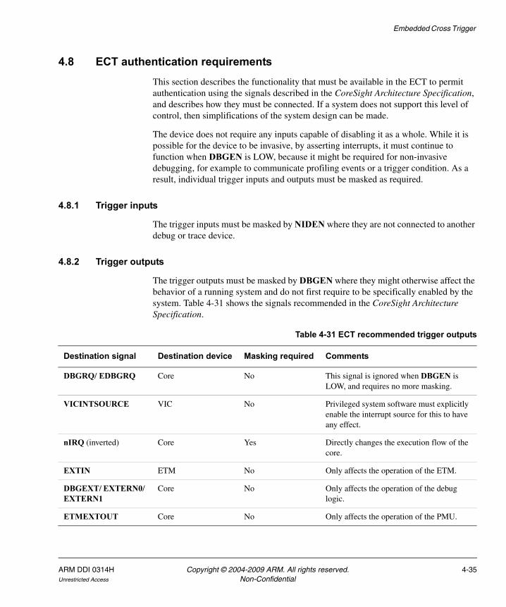
Embedded Cross Trigger
4.8 ECT authentication requirements This section describes the functionality that must be available in the ECT to permit authentication using the signals described in the CoreSight Architecture Specification, and describes how they must be connected. If a system does not support this level of control, then simplifications of the system design can be made.
The device does not require any inputs capable of disabling it as a whole. While it is possible for the device to be invasive, by asserting interrupts, it must continue to function when DBGEN is LOW, because it might be required for non-invasive debugging, for example to communicate profiling events or a trigger condition. As a result, individual trigger inputs and outputs must be masked as required.
4.8.1 Trigger inputs
The trigger inputs must be masked by NIDEN where they are not connected to another debug or trace device.
4.8.2 Trigger outputs
The trigger outputs must be masked by DBGEN where they might otherwise affect the behavior of a running system and do not first require to be specifically enabled by the system. Table 4-31 shows the signals recommended in the CoreSight Architecture Specification.
Table 4-31 ECT recommended trigger outputs
Destination signal Destination device Masking required Comments
DBGRQ/ EDBGRQ Core No This signal is ignored when DBGEN is LOW, and requires no more masking.
VICINTSOURCE VIC No Privileged system software must explicitly enable the interrupt source for this to have any effect.
nIRQ (inverted) Core Yes Directly changes the execution flow of the core.
EXTIN ETM No Only affects the operation of the ETM.
DBGEXT/ EXTERN0/ EXTERN1
Core No Only affects the operation of the debug logic.
ETMEXTOUT Core No Only affects the operation of the PMU.
ARM DDI 0314H Copyright © 2004-2009 ARM. All rights reserved. 4-35Unrestricted Access Non-Confidential
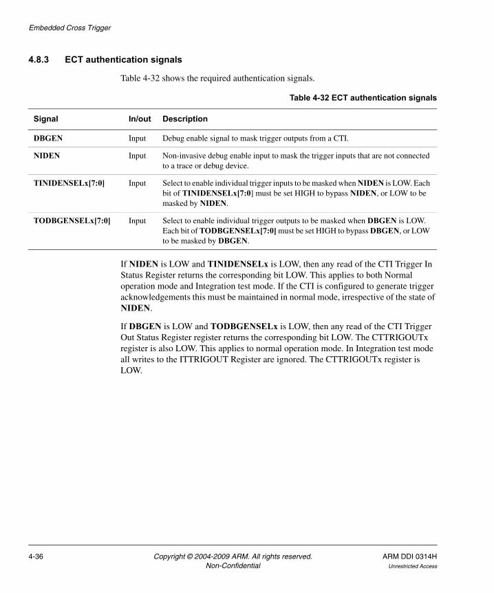
Embedded Cross Trigger
4.8.3 ECT authentication signals
Table 4-32 shows the required authentication signals.
If NIDEN is LOW and TINIDENSELx is LOW, then any read of the CTI Trigger In Status Register returns the corresponding bit LOW. This applies to both Normal operation mode and Integration test mode. If the CTI is configured to generate trigger acknowledgements this must be maintained in normal mode, irrespective of the state of NIDEN.
If DBGEN is LOW and TODBGENSELx is LOW, then any read of the CTI Trigger Out Status Register register returns the corresponding bit LOW. The CTTRIGOUTx register is also LOW. This applies to normal operation mode. In Integration test mode all writes to the ITTRIGOUT Register are ignored. The CTTRIGOUTx register is LOW.
Table 4-32 ECT authentication signals
Signal In/out Description
DBGEN Input Debug enable signal to mask trigger outputs from a CTI.
NIDEN Input Non-invasive debug enable input to mask the trigger inputs that are not connected to a trace or debug device.
TINIDENSELx[7:0] Input Select to enable individual trigger inputs to be masked when NIDEN is LOW. Each bit of TINIDENSELx[7:0] must be set HIGH to bypass NIDEN, or LOW to be masked by NIDEN.
TODBGENSELx[7:0] Input Select to enable individual trigger outputs to be masked when DBGEN is LOW. Each bit of TODBGENSELx[7:0] must be set HIGH to bypass DBGEN, or LOW to be masked by DBGEN.
4-36 Copyright © 2004-2009 ARM. All rights reserved. ARM DDI 0314HNon-Confidential Unrestricted Access
Chapter 5 ATB 1:1 Bridge
This chapter describes the AMBA Trace Bus (ATB) 1:1 bridge that enables design integrators to meet timing closure that can occur on an ATB system. It contains the following sections:
• About the ATB 1:1 bridge on page 5-2
• Authentication requirements for ATB 1:1 Bridge on page 5-4.
ARM DDI 0314H Copyright © 2004-2009 ARM. All rights reserved. 5-1Unrestricted Access Non-Confidential

ATB 1:1 Bridge
5.1 About the ATB 1:1 bridgeThe ATB 1:1 bridge consists of a set of registers across the data interface and the control signals that are emitted from trace sources. This bridge has two ATB interfaces, a slave and a master. Both interfaces exist in the same clock domain which is why it is referred to as a 1:1 bridge.
There are no programmable registers and the component appears transparent.
5.1.1 Normal operation
The synchronous bridge acts as a buffering element and adds a minimum of one clock cycle delay to ATB transactions. As shown in Figure 5-1, when the buffer is empty it can assert ATREADYS and can accept a packet of data from the trace source, ATVALIDS. When the buffer is full, this can be indicated using ATVALIDM and then the buffer can be emptied when ATREADYM goes HIGH.
Figure 5-1 ATB basic operation
5.1.2 Flushing operation
Figure 5-2 on page 5-3 shows how a flush appears on the two interfaces to the bridge. All signals are registered so AFVALIDS goes HIGH one cycle later than AFVALIDM. This also causes a cycle delay of the flush acknowledgement, AFREADYS to AFREADYM.
ATCLK
ATVALIDM
ATREADYM
ATVALIDS
ATREADYS
Empty Full
5-2 Copyright © 2004-2009 ARM. All rights reserved. ARM DDI 0314HNon-Confidential Unrestricted Access
ATB 1:1 Bridge
Figure 5-2 ATB flushing operation on master and slave interfaces
5.1.3 Flushing and data packets
The return of AFREADYM must be held up if there is data associated with the flush event. The indication of the flush completion must be delayed until all historical data has been transmitted. This includes data stored within the synchronous bridge.
Figure 5-3 shows an example of such a sequence. AFREADYM is only indicated after AFREADYS has been captured, from the trace source, and the data packet within the bridge has been accepted by ATREADYM, the trace sink.
Figure 5-3 ATB flushing data packets
ATCLK
AFVALIDM
AFREADYM
AFVALIDS
AFREADYS
ATCLK
AFVALIDM
AFREADYM
AFVALIDS
AFREADYS
ATVALIDM
ATREADYM
ATVALIDS
ATREADYS
ARM DDI 0314H Copyright © 2004-2009 ARM. All rights reserved. 5-3Unrestricted Access Non-Confidential
ATB 1:1 Bridge
5.2 Authentication requirements for ATB 1:1 BridgeNo disable inputs are required because this component has no effect on the ATB data.
5-4 Copyright © 2004-2009 ARM. All rights reserved. ARM DDI 0314HNon-Confidential Unrestricted Access
Chapter 6 ATB Replicator
This chapter describes the AMBA Trace Bus (ATB) replicator. The ATB replicator enables two trace sinks to be wired together and operate from the same incoming trace stream. It contains the following sections:
• About the ATB replicator on page 6-2
• ATB replicator connection behavior on page 6-3
• Authentication requirements for replicators on page 6-5.
ARM DDI 0314H Copyright © 2004-2009 ARM. All rights reserved. 6-1Unrestricted Access Non-Confidential

ATB Replicator
6.1 About the ATB replicatorThe ATB replicator enables two trace sinks to be wired together and to operate from the same incoming trace stream. There are no programmable registers. This component is invisible to you on a particular trace path, from source to sink. Figure 6-1 shows the example ATB replicator.
Figure 6-1 Example ATB replicator
6.1.1 Incoming ATB interface
The ATB replicator accepts trace data from a trace source, either directly or through a trace funnel.
6.1.2 Outgoing ATB interfaces
The ATB replicator sends identical trace data on outgoing master port interfaces.
ATB Input Slave Port
ATB Output Master Port 0
ATB OutputMaster Port1
6-2 Copyright © 2004-2009 ARM. All rights reserved. ARM DDI 0314HNon-Confidential Unrestricted Access
ATB Replicator
6.2 ATB replicator connection behaviorThe ATB replicator is a rewiring unit for the connection of two trace sinks. Buses cannot be connected directly together.
The only design considerations are for:
• ATREADY to the incoming ATB
• ATVALID to the outgoing ATBs
• AFVALID to the incoming ATB.
Because of the simplicity of the block, no programmers model exists for this block. It is a requirement of the attached trace sinks to set their ATREADY signal when they are disabled. This enables the replicator to operate as a pass-through to the remaining enable trace sink.
Any connected blocks, on both the inputs and the outputs, must operate on the same ATCLK domain.
6.2.1 ATREADYS and ATVALIDM
The ATREADYS to the original trace source can only be asserted when both of the trace outputs have accepted the current packet. One or both connected trace sinks might be disabled. If so, they must tie ATREADYS HIGH.
Because the trace sinks accept the trace data at different moments, the ATVALIDM signal to them is not asserted immediately after they have read the data packet because the data packet must persist for the other trace sink. The ATVALIDM signal is valid only for new packets until a valid ATREADYM cycle is seen. If ATVALIDM is incorrectly asserted when an old data value is still present then this might cause a packet duplication to appear in the trace stream for that source. This is highly likely to create problems at decompression.
Devices that connect to the output of the Replicator, the TPIU and the ETB for example, must tie the ATREADYM signal HIGH when they are disabled. If connected devices do not do this they cause the trace stream to stop the other channel that might still be enabled. This removes the requirement for the replicator to be aware of the state of downstream components
6.2.2 Flushing AFVALIDM and AFREADYM
Whenever one of the trace sinks initiates a flush to remove old information from the system then the replicator must propagate this request even when the other sink has not requested it.
ARM DDI 0314H Copyright © 2004-2009 ARM. All rights reserved. 6-3Unrestricted Access Non-Confidential

ATB Replicator
This does not cause any problems with the non-requested trace sink. It receives the flushed data. If the second master port receives a request to start a flush when there is already a flush operation under way that was begun by the first master port, then the Replicator must wait until the first request is serviced and then hold AFVALIDS HIGH to service the second request.
Figure 6-2 shows the expected interactions of the three AFVALID and AFREADY signal pairs. A flush request is started on master port 0 at time t0 that propagates to the slave port interface, AFVALIDM0 to AFVALIDS. While this is still being serviced a second request is made, at time t1, but on master port 1, AFVALIDM1. At t2, the first request is completed by the indication of ATREADYS on the slave port. This causes AFREADYM0 to complete the flush request. Because of the second request being made, the Replicator holds AFVALIDS HIGH to initiate a second flush of the system that continues until AFREADYS goes HIGH a second time at time t3.
Figure 6-2 ATB replicator flushing behavior
ATCLK
AFVALIDM0
AFREADYM0
AFVALIDM1
AFREADYM1
AFVALIDS
AFREADYS
t0 t1 t2 t3
6-4 Copyright © 2004-2009 ARM. All rights reserved. ARM DDI 0314HNon-Confidential Unrestricted Access
ATB Replicator
6.3 Authentication requirements for replicatorsATB replicators do not require any inputs capable of disabling them.
ARM DDI 0314H Copyright © 2004-2009 ARM. All rights reserved. 6-5Unrestricted Access Non-Confidential

ATB Replicator
6-6 Copyright © 2004-2009 ARM. All rights reserved. ARM DDI 0314HNon-Confidential Unrestricted Access
Chapter 7 CoreSight Trace Funnel
This chapter describes the CoreSight Trace Funnel (CSTF). It contains the following sections:
• About the CoreSight Trace Funnel on page 7-2
• CSTF programmers model on page 7-3
• CSTF specific registers on page 7-5
• CSTF Integration Test Registers on page 7-9
• CoreSight management registers for CSTF on page 7-15
• Unconnected slave interfaces on page 7-17
• Disabled slave interfaces on page 7-18
• CSTF input arbitration on page 7-19
• Authentication requirements for funnels on page 7-26.
ARM DDI 0314H Copyright © 2004-2009 ARM. All rights reserved. 7-1Unrestricted Access Non-Confidential
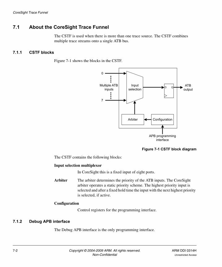
CoreSight Trace Funnel
7.1 About the CoreSight Trace FunnelThe CSTF is used when there is more than one trace source. The CSTF combines multiple trace streams onto a single ATB bus.
7.1.1 CSTF blocks
Figure 7-1 shows the blocks in the CSTF.
Figure 7-1 CSTF block diagram
The CSTF contains the following blocks:
Input selection multiplexor
In CoreSight this is a fixed input of eight ports.
Arbiter The arbiter determines the priority of the ATB inputs. The CoreSight arbiter operates a static priority scheme. The highest priority input is selected and after a fixed hold time the input with the next highest priority is selected, if active.
Configuration
Control registers for the programming interface.
7.1.2 Debug APB interface
The Debug APB interface is the only programming interface.
0
7
Multiple ATB inputs
Arbiter
APB programming interface
Configuration
Input selection
D Q ATB output
7-2 Copyright © 2004-2009 ARM. All rights reserved. ARM DDI 0314HNon-Confidential Unrestricted Access
CoreSight Trace Funnel
7.2 CSTF programmers modelTable 7-1 shows the CSTF registers.
Table 7-1 CSTF visible registers
Offset Type Width Reset value Name Description
0x000 R/W 12 0x300 Funnel Control Register CSTF Control Register, 0x000 on page 7-5
0x004 R/W 24 0xFAC688 Priority Control Register CSTF Priority Control Register, 0x004 on page 7-6
0xEEC R/W 5 0x00 Integration Register, ITATBDATA0 CSTF Integration Test Registers on page 7-9
0xEF0 R/W 2 0x0 Integration Register, ITATBCTR2 CSTF Integration Test Registers on page 7-9
0xEF4 R/W 7 0x00 Integration Register, ITATBCTR1 CSTF Integration Test Registers on page 7-9
0xEF8 R/W 10 0x000 Integration Register, ITATBCTR0 CSTF Integration Test Registers on page 7-9
0xF00 R/W 1 0x0 Integration Mode Control Register CoreSight management registers for CSTF on page 7-15
0xFA0 R/W 4 0xF Claim Tag Set Register
0xFA4 R/W 4 0x0 Claim Tag Clear Register
0xFB0 WO 32 - Lock Access
0xFB4 RO 3 0x0/0x3 Lock Status
0xFB8 RO 8 0x00 Authentication status
0xFC8 RO 8 0x28 Device ID
0xFCC RO 8 0x12 Device Type Identifier
0xFD0 RO 8 0x04 Peripheral ID4
0xFD4 RO 8 0x00 Peripheral ID5
0xFD8 RO 8 0x00 Peripheral ID6
0xFDC RO 8 0x00 Peripheral ID7
0xFE0 RO 8 0x08 Peripheral ID0
ARM DDI 0314H Copyright © 2004-2009 ARM. All rights reserved. 7-3Unrestricted Access Non-Confidential

CoreSight Trace Funnel
0xFE4 RO 8 0xB9 Peripheral ID1 CoreSight management registers for CSTF on page 7-15
0xFE8 RO 8 0x1B Peripheral ID2
0xFEC RO 8 0x00 Peripheral ID3
0xFF0 RO 8 0x0D Component ID0
0xFF4 RO 8 0x90 Component ID1
0xFF8 RO 8 0x05 Component ID2
0xFFC RO 8 0xB1 Component ID3
Table 7-1 CSTF visible registers (continued)
Offset Type Width Reset value Name Description
7-4 Copyright © 2004-2009 ARM. All rights reserved. ARM DDI 0314HNon-Confidential Unrestricted Access
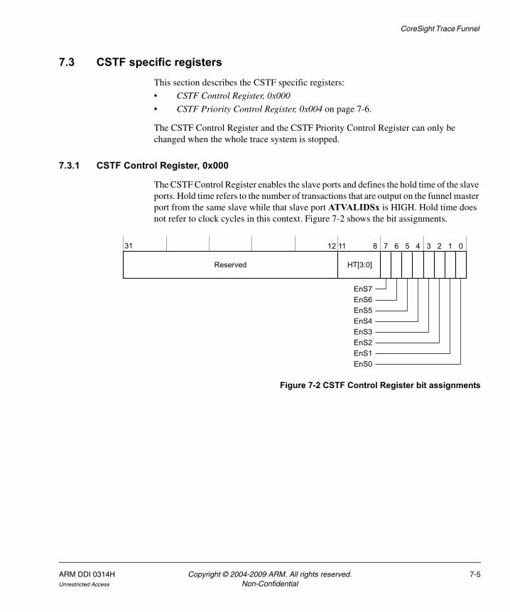
CoreSight Trace Funnel
7.3 CSTF specific registersThis section describes the CSTF specific registers:
• CSTF Control Register, 0x000
• CSTF Priority Control Register, 0x004 on page 7-6.
The CSTF Control Register and the CSTF Priority Control Register can only be changed when the whole trace system is stopped.
7.3.1 CSTF Control Register, 0x000
The CSTF Control Register enables the slave ports and defines the hold time of the slave ports. Hold time refers to the number of transactions that are output on the funnel master port from the same slave while that slave port ATVALIDSx is HIGH. Hold time does not refer to clock cycles in this context. Figure 7-2 shows the bit assignments.
Figure 7-2 CSTF Control Register bit assignments
31 4 3 2 1
Reserved
0
EnS7
12 11 5678
HT[3:0]
EnS6EnS5EnS4EnS3EnS2EnS1EnS0
ARM DDI 0314H Copyright © 2004-2009 ARM. All rights reserved. 7-5Unrestricted Access Non-Confidential
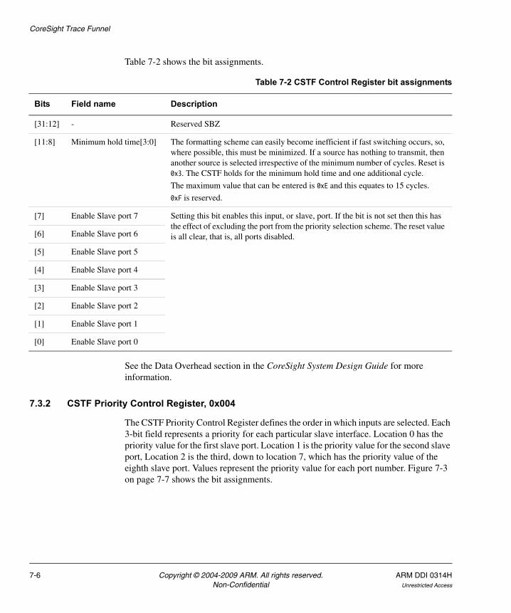
CoreSight Trace Funnel
Table 7-2 shows the bit assignments.
See the Data Overhead section in the CoreSight System Design Guide for more information.
7.3.2 CSTF Priority Control Register, 0x004
The CSTF Priority Control Register defines the order in which inputs are selected. Each 3-bit field represents a priority for each particular slave interface. Location 0 has the priority value for the first slave port. Location 1 is the priority value for the second slave port, Location 2 is the third, down to location 7, which has the priority value of the eighth slave port. Values represent the priority value for each port number. Figure 7-3 on page 7-7 shows the bit assignments.
Table 7-2 CSTF Control Register bit assignments
Bits Field name Description
[31:12] - Reserved SBZ
[11:8] Minimum hold time[3:0] The formatting scheme can easily become inefficient if fast switching occurs, so, where possible, this must be minimized. If a source has nothing to transmit, then another source is selected irrespective of the minimum number of cycles. Reset is 0x3. The CSTF holds for the minimum hold time and one additional cycle.
The maximum value that can be entered is 0xE and this equates to 15 cycles.
0xF is reserved.
[7] Enable Slave port 7 Setting this bit enables this input, or slave, port. If the bit is not set then this has the effect of excluding the port from the priority selection scheme. The reset value is all clear, that is, all ports disabled.[6] Enable Slave port 6
[5] Enable Slave port 5
[4] Enable Slave port 4
[3] Enable Slave port 3
[2] Enable Slave port 2
[1] Enable Slave port 1
[0] Enable Slave port 0
7-6 Copyright © 2004-2009 ARM. All rights reserved. ARM DDI 0314HNon-Confidential Unrestricted Access
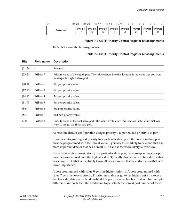
CoreSight Trace Funnel
Figure 7-3 CSTF Priority Control Register bit assignments
Table 7-3 shows the bit assignments.
At reset the default configuration assigns priority 0 to port 0, and priority 1 to port 1.
If you want to give highest priority to a particular slave port, the corresponding port must be programmed with the lowest value. Typically this is likely to be a port that has more important data or that has a small FIFO and is therefore likely to overflow.
If you want to give lowest priority to a particular slave port, the corresponding slave port must be programmed with the highest value. Typically this is likely to be a device that has a large FIFO that is less likely to overflow or a source that has information that is of lower importance.
A port programmed with value 0 gets the highest priority. A port programmed with value 7 gets the lowest priority.Priority must always go to the highest priority source that has valid data available, if enabled. If a priority value has been entered for multiple different slave ports then the arbitration logic selects the lowest port number of them.
Reserved PriPort 2
PriPort 3
PriPort 4
PriPort 5
PriPort 6
PriPort 7
PriPort 1
PriPort 0
31 24 23 21 20 18 17 15 14 12 11 9 8 6 5 3 2 0
Table 7-3 CSTF Priority Control Register bit assignments
Bits Field name Description
[31:24] - Reserved.
[23:21] PriPort 7 Priority value of the eighth port. The value written into this location is the value that you want to assign the eighth slave port.
[20:18] PriPort 6 7th port priority value.
[17:15] PriPort 5 6th port priority value.
[14:12] PriPort 4 5th port priority value.
[11:9] PriPort 3 4th port priority value.
[8:6] PriPort 2 3rd port priority value.
[5:3] PriPort 1 2nd port priority value.
[2:0] PriPort 0 Priority value of the first slave port. The value written into this location is the value that you want to assign the first slave port.
ARM DDI 0314H Copyright © 2004-2009 ARM. All rights reserved. 7-7Unrestricted Access Non-Confidential

CoreSight Trace Funnel
Note This register must only be altered when the trace system is disabled, that is, trace sources are off and the system is drained.
7-8 Copyright © 2004-2009 ARM. All rights reserved. ARM DDI 0314HNon-Confidential Unrestricted Access
CoreSight Trace Funnel
7.4 CSTF Integration Test RegistersIntegration Test Registers are provided to simplify the process of verifying the integration of the CSTF with other devices in a CoreSight system. These registers enable direct control of outputs and the ability to read the value of inputs. You must only use these registers when the Integration Mode Control Register (0xF00) bit [0] is set to 1.
There must be no trace in the system when you use the Integration registers. You use the same integration registers to check all the ATB slave interfaces in addition to the ATB master interface. To select which slave interface is connected to the integration registers, you must select the interface using the CSTF Control register at 0x000. For integration purposes you must only enable one port at any time. When checking the ATB master port, the value of the CSTF Control Register has no effect.
For example, to read the ATVALIDS1 input the CSTF Control Register must be set to 0x02 to only select slave port 1, then a read of ITATBCTR0 bit 0 yields the value of ATVALIDS1.
To set the value of ATVALIDM, the value in the CSTF Control Register is irrelevant and a write to ITATBCTR0 bit 0 sets the value of ATVALIDM.
For full details of how to use the integration registers in a system to verify the integration of multiple devices see the CoreSight Components Implementation Guide and the applicable Integration Manual.
7.4.1 CSTF Integration Test Registers
This sections describes the following registers:
• Integration Test ATB Data 0 Register, ITATBDATA0, 0xEEC
• Integration Test ATB Control 2 Register, ITATBCTR2, 0xEF0 on page 7-11
• Integration Test ATB Control 1 Register, ITATBCTR1, 0xEF4 on page 7-12
• Integration Test ATB Control 0 Register, ITATBCTR0, 0xEF8 on page 7-13.
Integration Test ATB Data 0 Register, ITATBDATA0, 0xEEC
The Integration Test ATB Data 0 Register performs different functions depending on whether the access is a read or a write:
• A write outputs data on ATDATAM.
• A read returns the data from ATDATAS<n>, where <n> is defined by the status of the CSTF Control register at 0x000. The read data is only valid when ATVALIDS<n> is HIGH.
Figure 7-4 on page 7-10 shows the bit assignments.
ARM DDI 0314H Copyright © 2004-2009 ARM. All rights reserved. 7-9Unrestricted Access Non-Confidential
CoreSight Trace Funnel
Figure 7-4 Integration Test ATB Data 0 Register bit assignments
Table 7-4 shows the bit assignments for this register on reads.
Table 7-5 shows the bit assignments for this register on writes.
31 4 3 2 1
Reserved
0
ATDATA[31]ATDATA[23]ATDATA[15]
ATDATA[0]ATDATA[7]
5
Table 7-4 Integration Test ATB Data 0 Register bit assignments on reads
Bits Type Name Function
[31:5] - - Reserved
[4] RO ATDATA[31] Read the value of ATDATAS<31>
[3] RO ATDATA[23] Read the value of ATDATAS<23>
[2] RO ATDATA[15] Read the value of ATDATAS<15>
[1] RO ATDATA[7] Read the value of ATDATAS<7>
[0] RO ATDATA[0] Read the value of ATDATAS<0>
Table 7-5 Integration Test ATB Data 0 Register bit assignments on writes
Bits Type Name Function
[31:5] - - Reserved
[4] WO ATDATA[31] Set the value of ATDATAM[31]
[3] WO ATDATA[23] Set the value of ATDATAM[23]
[2] WO ATDATA[15] Set the value of ATDATAM[15]
[1] WO ATDATA[7] Set the value of ATDATAM[7]
[0] WO ATDATA[0] Set the value of ATDATAM[0]
7-10 Copyright © 2004-2009 ARM. All rights reserved. ARM DDI 0314HNon-Confidential Unrestricted Access
CoreSight Trace Funnel
Integration Test ATB Control 2 Register, ITATBCTR2, 0xEF0
The Integration Test ATB Control 2 Register performs different functions depending on whether the access is a read or a write:
• A write outputs data on ATREADYS<n> and AFVALIDS<n>, where <n> is defined by the status of the CSTF Control Register at 0x000
• A read returns the data from ATREADYM and AFVALIDM.
Figure 7-5 shows the bit assignments.
Figure 7-5 Integration Test ATB Control 2 Register bit assignments
Table 7-6 shows the bit assignments on reads.
Table 7-7 shows the bit assignments on writes.
31
Reserved
01
AFVALIDATREADY
Table 7-6 Integration Test ATB Control 2 Register bit assignments on reads
Bits Type Name Function
[31:2] - - Reserved
[1] RO AFVALID Read the value of AFVALIDM
[0] RO ATREADY Read the value of ATREADYM
Table 7-7 Integration Test ATB Control 2 Register bit assignments on writes
Bits Type Name Function
[31:2] - - Reserved
[1] WO AFVALID Set the value of AFVALIDS<n>
[0] WO ATREADY Set the value of AFREADYS<n>
ARM DDI 0314H Copyright © 2004-2009 ARM. All rights reserved. 7-11Unrestricted Access Non-Confidential
CoreSight Trace Funnel
Integration Test ATB Control 1 Register, ITATBCTR1, 0xEF4
The Integration Test ATB Control 1 Register performs different functions depending on whether the access is a read or a write:
• A write outputs data on ATIDM.
• A read returns the data from ATIDS<n>, where <n> is defined by the status of the CSTF Control register at 0x000. The read data is only valid when ATVALIDS<n> is HIGH.
ITATBCTR1 contains the value of the ATIDS input to the CSTF. Figure 7-6 shows the bit assignments.
Figure 7-6 Integration Test ATB Control 1 Register bit assignments
Table 7-8 shows the bit assignments on reads.
Table 7-9 shows the bit assignments on writes.
31
Reserved
6 0
ATID
7
Table 7-8 Integration Test ATB Control 1 Register bit assignments on reads
Bits Type Name Function
[31:7] - - Reserved
[6:0] RO ATID Read the value of ATIDS
Table 7-9 Integration Test ATB Control 1 Register bit assignments on writes
Bits Type Name Function
[31:7] - - Reserved
[6:0] WO ATID Set the value of ATIDM
7-12 Copyright © 2004-2009 ARM. All rights reserved. ARM DDI 0314HNon-Confidential Unrestricted Access

CoreSight Trace Funnel
Integration Test ATB Control 0 Register, ITATBCTR0, 0xEF8
The Integration Test ATB Control 0 Register performs different functions depending on whether the access is a read or a write:
• a write sets the value of the ATVALIDM, AFREADYM, and ATBYTESM signals.
• a read returns the value of the ATVALIDS<n>, AFREADYS<n>, and ATBYTESS<n> signals, where <n> is defined by the status of the CSTF Control register at 0x000. The read value of ATBYTESS<n> is only valid when ATVALIDS<n> is HIGH.
Figure 7-7 shows the bit assignments.
Figure 7-7 Integration Test ATB Control 0 Register bit assignments
Table 7-10 shows the bit assignments for this register on reads.
31
Reserved
01
AFREADYATVALID
9 8
Reserved
ATBYTES
10 7 2
Table 7-10 Integration Test ATB Control 1 Register bit assignments on reads
Bits Type Name Function
[31:10] - - Reserved
[9:8] RO ATBYTES Read the value of ATBYTESS<n>
[7:2] - - Reserved
[1] RO AFREADYS Read the value of AFREADYS<n>
[0] RO ATVALID Read the value of ATVALIDS<n>
ARM DDI 0314H Copyright © 2004-2009 ARM. All rights reserved. 7-13Unrestricted Access Non-Confidential
CoreSight Trace Funnel
Table 7-11 shows the bit assignments for this register on writes.
Table 7-11 Integration Test ATB Control 0 Register bit assignments on writes
Bits Type Name Function
[31:10] - - Reserved
[9:8] WO ATBYTES Set the value of ATBYTESM
[7:2] - - Reserved
[1] WO AFREADYS Set the value of AFREADYM
[0] WO ATVALID Set the value of ATVALIDM
7-14 Copyright © 2004-2009 ARM. All rights reserved. ARM DDI 0314HNon-Confidential Unrestricted Access
CoreSight Trace Funnel
7.5 CoreSight management registers for CSTFThis section gives information specific to the CSTF programmable registers.
Claim tags, 0xFA0 and 0xFA4
The CSTF implements a four-bit claim tag. The use of bits [3:0] is software defined.
Lock access mechanism, 0xFB0 and 0xFB4
The CSTF implements two memory maps controlled through PADDRDBG31. When PADDRDBG31 is HIGH, the Lock Status Register reads as 0x0 indicating that no lock exists. When PADDRDBG31 is LOW, the Lock Status Register reads as 0x3 from reset. This indicates a 32-bit lock access mechanism is present and is locked.
Authentication Status, 0xFB8 [7:0]
Reports the required security level. This is set to 0x00 for functionality not implemented.
Device ID, 0xFC8 The CSTF has the default value of 0x28. Table 7-12 shows the Device ID bit assignments.
Device Type Identifier, 0xFCC [7:0]
A value of 0x12 identifies this device as a trace link (0x2) and specifically as a funnel/router (0x1).
PartNumber, 0xFE4 [3:0], 0xFE0 [7:4], 0xFE0 [3:0]
Upper, middle, and lower BCD value of Device number. Set to 0x908.
Designer JEP106 value, 0xFD0[3:0], 0xFE8[2:0], 0xFE4[7:4]
The CSTF is identified as an ARM component with a JEP106 identity at 0x3B and a JEP106 continuation code at 0x4 (fifth bank).
Table 7-12 CSTF Device ID bit assignments
Bits Value Description
[31:8] 0x000000 Reserved.
[7:4] 0x2 The CSTF implements a static priority scheme.
[3:0] 0x8 This is the value of the Verilog define PORTCOUNT and represents the number of input ports connected. By default all 8 ports are connected. 0x0 and 0x1 are illegal values.
ARM DDI 0314H Copyright © 2004-2009 ARM. All rights reserved. 7-15Unrestricted Access Non-Confidential
CoreSight Trace Funnel
Component class, 0xFF4[7:4]
The CSTF complies to the CoreSight class of components and this value is set to 0x9.
See Table 1-1 on page 1-4 for the current value of the revision field at offset 0xFE8[7:4].
7-16 Copyright © 2004-2009 ARM. All rights reserved. ARM DDI 0314HNon-Confidential Unrestricted Access

CoreSight Trace Funnel
7.6 Unconnected slave interfacesThe CSTF is fixed as an eight-input device. Not all eight inputs might be required. When unused ports are present these must be suitably tied off as shown in Table 7-13. If ports are unconnected but not disabled, the operation is UNPREDICTABLE.
Table 7-13 Tie-offs for unconnected ports
Port name Tie-off value
ATIDSx[6:0] None required but a recommendation of 7'b0000000
ATDATASx[31:0] None required but a recommendation of 32'h00000000
ATVALIDSx 1'b0
ATBYTESSx[1:0] None required but a recommendation of 2'b00
ATREADYSx None required because this is an output
AFVALIDSx None required because this is an output
AFREADYSx 1'b1
ARM DDI 0314H Copyright © 2004-2009 ARM. All rights reserved. 7-17Unrestricted Access Non-Confidential
CoreSight Trace Funnel
7.7 Disabled slave interfacesWhen a slave interface is disabled, that is, the corresponding bit is cleared in the Funnel Control Register, the interface returns ATREADYx HIGH and AFALIDx LOW.
7-18 Copyright © 2004-2009 ARM. All rights reserved. ARM DDI 0314HNon-Confidential Unrestricted Access
CoreSight Trace Funnel
7.8 CSTF input arbitrationTypical arbiters in AHB systems use a simple fixed priority scheme. This reduces the required complexity of the arbiter and also removes any direct user control in programmable registers. To ensure maximum flexibility is obtained before intended use is decided, the arbitration scheme used in the CSTF is more flexible than the simple fixed priority.
7.8.1 Static priority
Static priority is a small expansion of the standard fixed priority scheme. Rather than dictate the priorities of the inputs at the design stage, this can be altered before any trace capture is begun to enable refinement of input priority ordering for different requirements. The advantage of this scheme compared to the fixed version is that the integrator does not have to know trace usage requirements that might change depending on the particular application.
7.8.2 Minimum hold time
The Funnel Control Register enables slave inputs of the funnel to be held for a number of cycles before the arbiter logic changes to a higher priority source. This value is the minimum number of cycles of data that are output from a source before a change to a higher priority is performed, plus 1, that is, a value of 0x0 indicates a minimum hold time of 1 and a value of 0x5, indicates a minimum hold time of six cycles. Large values enable the formatter in an ETB or TPIU to be less wasteful by having to indicate source changes in the protocol. These source changes reduce the amount of bandwidth available for trace data.
Figure 7-8 on page 7-20 shows an example of how a minimum hold time of two cycles stops the change of the arbiter from Slave1, ATVALIDS1 and ATREADYS1, even though a higher priority source indicates valid data, ATVALIDS0, after t0.
ARM DDI 0314H Copyright © 2004-2009 ARM. All rights reserved. 7-19Unrestricted Access Non-Confidential
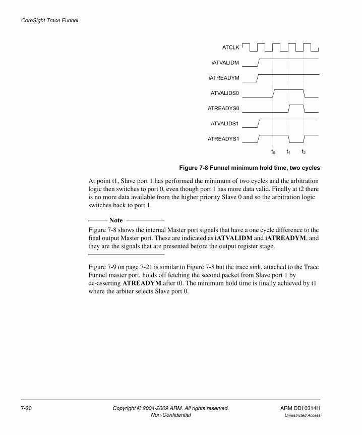
CoreSight Trace Funnel
Figure 7-8 Funnel minimum hold time, two cycles
At point t1, Slave port 1 has performed the minimum of two cycles and the arbitration logic then switches to port 0, even though port 1 has more data valid. Finally at t2 there is no more data available from the higher priority Slave 0 and so the arbitration logic switches back to port 1.
Note Figure 7-8 shows the internal Master port signals that have a one cycle difference to the final output Master port. These are indicated as iATVALIDM and iATREADYM, and they are the signals that are presented before the output register stage.
Figure 7-9 on page 7-21 is similar to Figure 7-8 but the trace sink, attached to the Trace Funnel master port, holds off fetching the second packet from Slave port 1 by de-asserting ATREADYM after t0. The minimum hold time is finally achieved by t1 where the arbiter selects Slave port 0.
ATCLK
iATVALIDM
iATREADYM
ATVALIDS0
ATREADYS0
ATVALIDS1
ATREADYS1
t0 t1 t2
7-20 Copyright © 2004-2009 ARM. All rights reserved. ARM DDI 0314HNon-Confidential Unrestricted Access
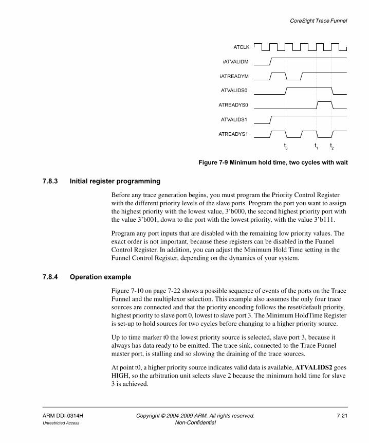
CoreSight Trace Funnel
Figure 7-9 Minimum hold time, two cycles with wait
7.8.3 Initial register programming
Before any trace generation begins, you must program the Priority Control Register with the different priority levels of the slave ports. Program the port you want to assign the highest priority with the lowest value, 3’b000, the second highest priority port with the value 3’b001, down to the port with the lowest priority, with the value 3’b111.
Program any port inputs that are disabled with the remaining low priority values. The exact order is not important, because these registers can be disabled in the Funnel Control Register. In addition, you can adjust the Minimum Hold Time setting in the Funnel Control Register, depending on the dynamics of your system.
7.8.4 Operation example
Figure 7-10 on page 7-22 shows a possible sequence of events of the ports on the Trace Funnel and the multiplexor selection. This example also assumes the only four trace sources are connected and that the priority encoding follows the reset/default priority, highest priority to slave port 0, lowest to slave port 3. The Minimum HoldTime Register is set-up to hold sources for two cycles before changing to a higher priority source.
Up to time marker t0 the lowest priority source is selected, slave port 3, because it always has data ready to be emitted. The trace sink, connected to the Trace Funnel master port, is stalling and so slowing the draining of the trace sources.
At point t0, a higher priority source indicates valid data is available, ATVALIDS2 goes HIGH, so the arbitration unit selects slave 2 because the minimum hold time for slave 3 is achieved.
ATCLK
iATVALIDM
iATREADYM
ATVALIDS0
ATREADYS0
ATVALIDS1
ATREADYS1
t0 t1 t2
ARM DDI 0314H Copyright © 2004-2009 ARM. All rights reserved. 7-21Unrestricted Access Non-Confidential
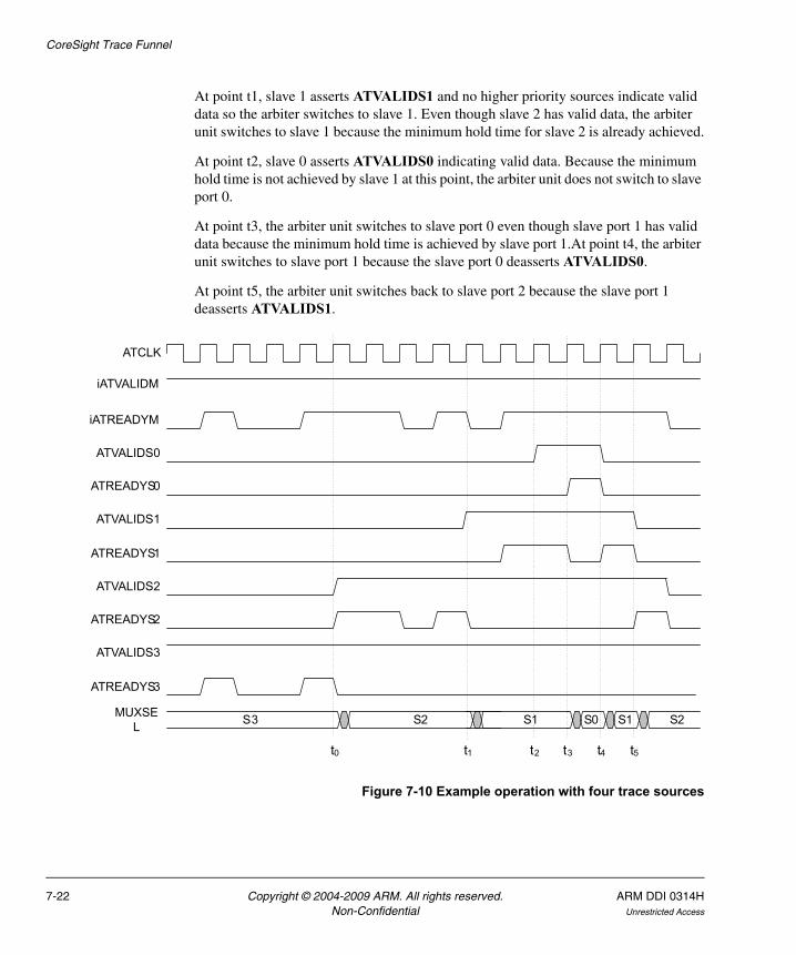
CoreSight Trace Funnel
At point t1, slave 1 asserts ATVALIDS1 and no higher priority sources indicate valid data so the arbiter switches to slave 1. Even though slave 2 has valid data, the arbiter unit switches to slave 1 because the minimum hold time for slave 2 is already achieved.
At point t2, slave 0 asserts ATVALIDS0 indicating valid data. Because the minimum hold time is not achieved by slave 1 at this point, the arbiter unit does not switch to slave port 0.
At point t3, the arbiter unit switches to slave port 0 even though slave port 1 has valid data because the minimum hold time is achieved by slave port 1.At point t4, the arbiter unit switches to slave port 1 because the slave port 0 deasserts ATVALIDS0.
At point t5, the arbiter unit switches back to slave port 2 because the slave port 1 deasserts ATVALIDS1.
Figure 7-10 Example operation with four trace sources
t0 t1 t4 t5
MUXSEL S3 S2 S0S1 S1 S2
ATCLK
iATVALIDM
iATREADYM
ATVALIDS0
ATREADYS0
ATVALIDS1
ATREADYS1
ATVALIDS2
ATREADYS2
ATVALIDS3
ATREADYS3
t2 t3
7-22 Copyright © 2004-2009 ARM. All rights reserved. ARM DDI 0314HNon-Confidential Unrestricted Access
CoreSight Trace Funnel
7.8.5 Flushing
Flushing is the emptying of existing data from the trace source buffers before tracing new data begins. See the CoreSight Architecture Specification for more on flushing mechanisms. At all times during a flushing operation, all ATB signals must comply with the ATB protocol.
The behavior of the CSTF is that AFREADYM only responds HIGH when all Slave ports have returned AFREADYS HIGH.
On assertion of AFVALIDM to the CSTF, all the enabled slave ports must have their AFVALIDS signals asserted to ensure that the marker for flushing historical information is located at similar times. AFVALIDS must then remain asserted until the specific slave port responds with AFREADYS HIGH. AFVALIDS is deasserted on a port by port basis.
The CSTF flushing mechanism uses the funnel prioritization for flushing historical data from components connected to the funnel inputs.
When AFVALIDS is output HIGH on all CSTF slave ports, the first source to indicate that it has valid data, indicated by ATVALIDS HIGH, is accepted.
If multiple sources assert ATVALIDS HIGH on the same cycle, then the highest priority source is selected. When this source completes other sources can be serviced.
When the flush is complete for a particular trace source, it is ignored in the input selection priority selection scheme until all enabled inputs have completed the flush operation by returning AFREADYS HIGH. This occurs even if it might have more data available, that is, ATVALID is HIGH.
7.8.6 Flushing example
Figure 7-11 on page 7-25 has four sources connected to the first four slave ports and they are configured so that they are enabled with priorities reflecting their port number Slave port 0 is the highest priority, and port 3 is the lowest.
Before time t0, the system is under normal operation where different trace sources are selected according to the arbitration scheme, in this example slave port 2. At time t0 there is a request from the trace sink device to flush the system of historical data this request is then propagated onto the slave ports in the following cycle, at time t1. The CSTF, at this point, is then operating in a flushing mode where it selects each device that has not been drained in turn.
At time t1, CSTF selects slave port 1, highest priority with valid data, to drain first. At the same time the source connected to port 3 returns AFREADYS3, which causes AFVALIDS3 to be deasserted in the following cycle.
ARM DDI 0314H Copyright © 2004-2009 ARM. All rights reserved. 7-23Unrestricted Access Non-Confidential

CoreSight Trace Funnel
Draining of slave port 1 continues until time t2 where it responds with AFREADYS1. If all higher priority sources are already flushed, the CSTF then switches to the next highest priority source that is still to drain. In this example, slave port 2 is not selected. It is overridden because a higher priority port reports valid data that has not finished flushing, therefore slave port 0 is selected.
This continues until time t3 when AFREADYS0 goes HIGH and draining of slave port 2 can begin and which continues until time t4, AFREADYS2 going HIGH.
At time t4 all slave ports have responded with AFREADY HIGH. This indicates that there is no more historical information remaining at this level. This is indicated on AFREADYM with a HIGH response, that in turn results in AFVALIDM returning LOW. The flush sequence is now complete and the CSTF can return to normal operation, in this example by selecting slave port 1.
Slave port 1 is not selected for a second time before time t4 even though it is at a higher priority than slave port 2. This is because it has returned AFREADYS1 HIGH previously.
7-24 Copyright © 2004-2009 ARM. All rights reserved. ARM DDI 0314HNon-Confidential Unrestricted Access
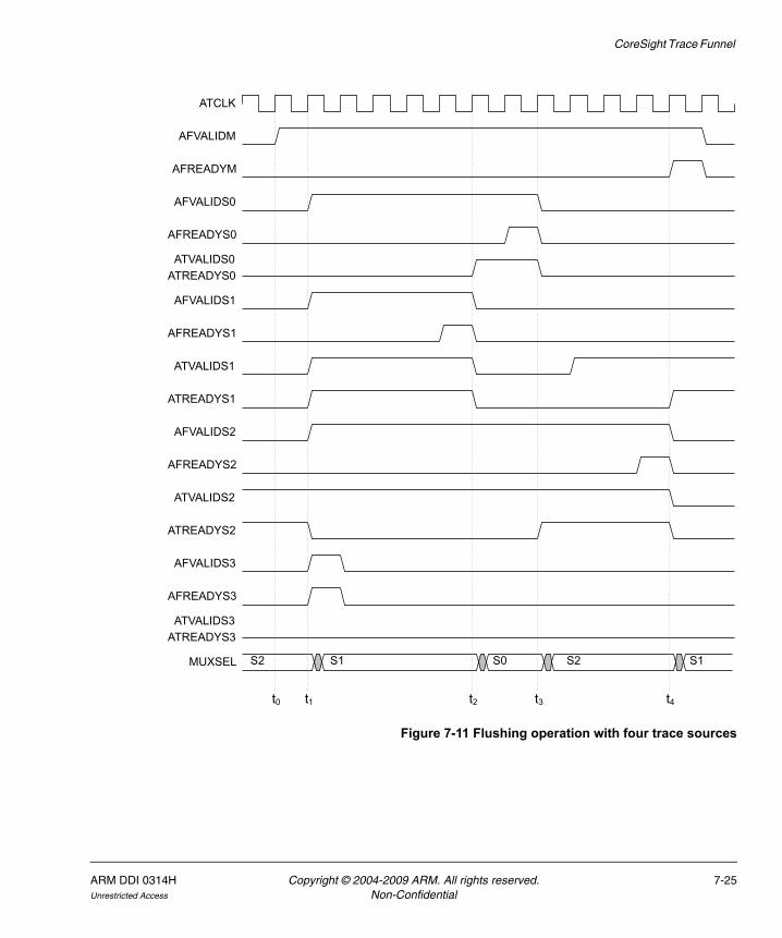
CoreSight Trace Funnel
Figure 7-11 Flushing operation with four trace sources
ATCLK
AFVALIDM
AFREADYM
AFVALIDS0
AFREADYS0
AFVALIDS1
AFREADYS1
AFVALIDS2
AFREADYS2
AFVALIDS3
AFREADYS3
ATVALIDS0ATREADYS0
ATVALIDS1
ATREADYS1
ATVALIDS2
ATREADYS3ATVALIDS3
ATREADYS2
MUXSEL S2 S1 S0 S2 S1
t0 t1 t2 t3 t4
ARM DDI 0314H Copyright © 2004-2009 ARM. All rights reserved. 7-25Unrestricted Access Non-Confidential
CoreSight Trace Funnel
7.9 Authentication requirements for funnelsFunnels do not require any inputs capable of disabling them.
7-26 Copyright © 2004-2009 ARM. All rights reserved. ARM DDI 0314HNon-Confidential Unrestricted Access

Chapter 8 Trace Port Interface Unit
This chapter describes the Trace Port Interface Unit (TPIU). It contains the following sections:
• About the Trace Port Interface Unit on page 8-2
• Trace Out Port on page 8-4
• Miscellaneous connections on page 8-5
• TPIU programmers model on page 8-6
• TPIU CoreSight management registers on page 8-9
• Trace port control registers on page 8-11
• TPIU trace port sizes on page 8-25
• TPIU triggers on page 8-27
• Other TPIU design considerations on page 8-29
• Authentication requirements for TPIUs on page 8-33
• TPIU pattern generator on page 8-34
• TPIU formatter and FIFO on page 8-36
• Configuration options on page 8-38
• Example configuration scenarios on page 8-39.
ARM DDI 0314H Copyright © 2004-2009 ARM. All rights reserved. 8-1Unrestricted Access Non-Confidential
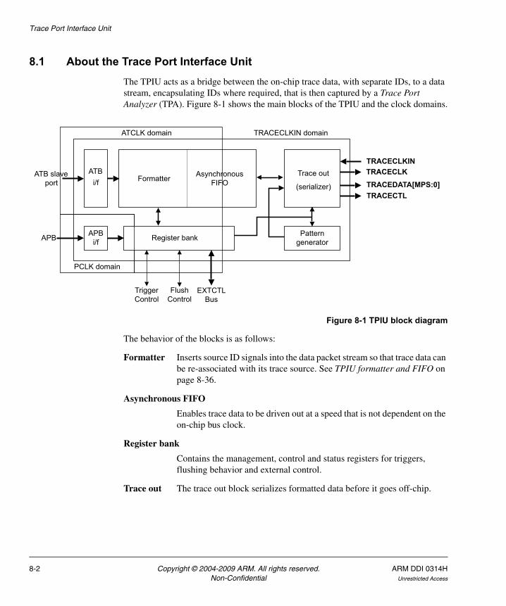
Trace Port Interface Unit
8.1 About the Trace Port Interface UnitThe TPIU acts as a bridge between the on-chip trace data, with separate IDs, to a data stream, encapsulating IDs where required, that is then captured by a Trace Port Analyzer (TPA). Figure 8-1 shows the main blocks of the TPIU and the clock domains.
Figure 8-1 TPIU block diagram
The behavior of the blocks is as follows:
Formatter Inserts source ID signals into the data packet stream so that trace data can be re-associated with its trace source. See TPIU formatter and FIFO on page 8-36.
Asynchronous FIFO
Enables trace data to be driven out at a speed that is not dependent on the on-chip bus clock.
Register bank
Contains the management, control and status registers for triggers, flushing behavior and external control.
Trace out The trace out block serializes formatted data before it goes off-chip.
PCLK domain
TRACECLKIN
APBi/f Register bank
FormatterTrace out
(serializer)
Pattern generatorAPB
TRACECTL
TRACECLKIN domain
EXTCTL Bus
TRACEDATA[MPS:0]TRACECLK
Flush Control
ATB slave port
ATBi/f
Trigger Control
AsynchronousFIFO
ATCLK domain
8-2 Copyright © 2004-2009 ARM. All rights reserved. ARM DDI 0314HNon-Confidential Unrestricted Access

Trace Port Interface Unit
Pattern Generator
The pattern generator unit provides a simple set of defined bit sequences or patterns that can be output over the Trace Port and be detected by the TPA or other associated Trace Capture Device (TCD). The TCD can use these patterns to indicate if it is possible to increase or to decrease the trace port clock speed. See TPIU pattern generator on page 8-34 for more information.
8.1.1 ATB interface
The TPIU accepts trace data from a trace source, either direct from a trace source or using a Trace Funnel.
8.1.2 APB interface
The APB interface is the programming interface for the TPIU.
ARM DDI 0314H Copyright © 2004-2009 ARM. All rights reserved. 8-3Unrestricted Access Non-Confidential
Trace Port Interface Unit
8.2 Trace Out PortTable 8-1 shows the Trace Out Port signals.
Table 8-1 Trace Out Port signals
Name Type Description
TRACECLKIN Input Decoupled clock from ATB to enable easy control of the trace port speed. This is typically derived from a controllable clock source on chip but could be driven by an external clock generator if a high speed pin is used. Data changes on the rising edge only. See Off-chip based TRACECLKIN on page 8-32 for more details of off-chip operated TRACECLKIN.
TRACECLK Output Exported version of TRACECLKIN. This is TRACECLKIN/2, and data changes on both rising edges and falling edges. See TRACECLK generation on page 8-29 for more details about TRACECLK generation.
TRACEDATA[MPS:0] Output Output data. MPS is TPMAXDATASIZE. See Supported Port Size Register, 0x000 on page 8-11.
TRACECTL Output Used to indicate nonvalid trace data and triggers. See Other TPIU design considerations on page 8-29.
TRESETn Input This is a reset signal for the TRACECLKIN domain. Because off-chip devices connect to the Trace Out port, this signal is related to the Trace Bus Resetting signal, ATRESETn.
TPCTL Input ASIC tie-off to report the presence of the TRACECTL pin. If TRACECTL is not present then this must be tied LOW. This input affects bit 2 of the Formatter and Flush Status Register. See Formatter and Flush Status Register, 0x300 on page 8-16.
TPMAXDATASIZE[4:0]
Input Tie-off to indicate the maximum TRACEDATA width available on the ASIC. The valid values are 1-32 (0x00-0x1F), for example if only a maximum of a 16-bit data port is available then this takes the value 0x0F. This input affects the Supported Port Size Register Supported Port Size Register, 0x000 on page 8-11.
8-4 Copyright © 2004-2009 ARM. All rights reserved. ARM DDI 0314HNon-Confidential Unrestricted Access
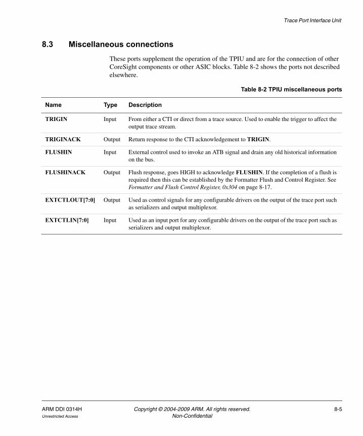
Trace Port Interface Unit
8.3 Miscellaneous connectionsThese ports supplement the operation of the TPIU and are for the connection of other CoreSight components or other ASIC blocks. Table 8-2 shows the ports not described elsewhere.
Table 8-2 TPIU miscellaneous ports
Name Type Description
TRIGIN Input From either a CTI or direct from a trace source. Used to enable the trigger to affect the output trace stream.
TRIGINACK Output Return response to the CTI acknowledgement to TRIGIN.
FLUSHIN Input External control used to invoke an ATB signal and drain any old historical information on the bus.
FLUSHINACK Output Flush response, goes HIGH to acknowledge FLUSHIN. If the completion of a flush is required then this can be established by the Formatter Flush and Control Register. See Formatter and Flush Control Register, 0x304 on page 8-17.
EXTCTLOUT[7:0] Output Used as control signals for any configurable drivers on the output of the trace port such as serializers and output multiplexor.
EXTCTLIN[7:0] Input Used as an input port for any configurable drivers on the output of the trace port such as serializers and output multiplexor.
ARM DDI 0314H Copyright © 2004-2009 ARM. All rights reserved. 8-5Unrestricted Access Non-Confidential
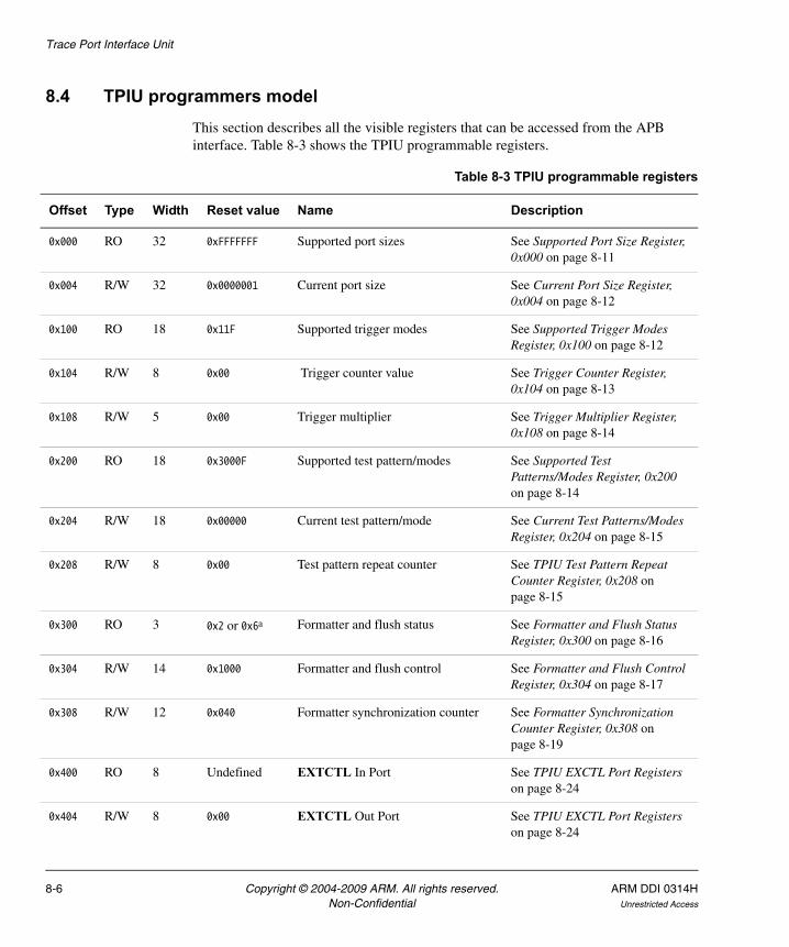
Trace Port Interface Unit
8.4 TPIU programmers modelThis section describes all the visible registers that can be accessed from the APB interface. Table 8-3 shows the TPIU programmable registers.
Table 8-3 TPIU programmable registers
Offset Type Width Reset value Name Description
0x000 RO 32 0xFFFFFFF Supported port sizes See Supported Port Size Register, 0x000 on page 8-11
0x004 R/W 32 0x0000001 Current port size See Current Port Size Register, 0x004 on page 8-12
0x100 RO 18 0x11F Supported trigger modes See Supported Trigger Modes Register, 0x100 on page 8-12
0x104 R/W 8 0x00 Trigger counter value See Trigger Counter Register, 0x104 on page 8-13
0x108 R/W 5 0x00 Trigger multiplier See Trigger Multiplier Register, 0x108 on page 8-14
0x200 RO 18 0x3000F Supported test pattern/modes See Supported Test Patterns/Modes Register, 0x200 on page 8-14
0x204 R/W 18 0x00000 Current test pattern/mode See Current Test Patterns/Modes Register, 0x204 on page 8-15
0x208 R/W 8 0x00 Test pattern repeat counter See TPIU Test Pattern Repeat Counter Register, 0x208 on page 8-15
0x300 RO 3 0x2 or 0x6a Formatter and flush status See Formatter and Flush Status Register, 0x300 on page 8-16
0x304 R/W 14 0x1000 Formatter and flush control See Formatter and Flush Control Register, 0x304 on page 8-17
0x308 R/W 12 0x040 Formatter synchronization counter See Formatter Synchronization Counter Register, 0x308 on page 8-19
0x400 RO 8 Undefined EXTCTL In Port See TPIU EXCTL Port Registers on page 8-24
0x404 R/W 8 0x00 EXTCTL Out Port See TPIU EXCTL Port Registers on page 8-24
8-6 Copyright © 2004-2009 ARM. All rights reserved. ARM DDI 0314HNon-Confidential Unrestricted Access
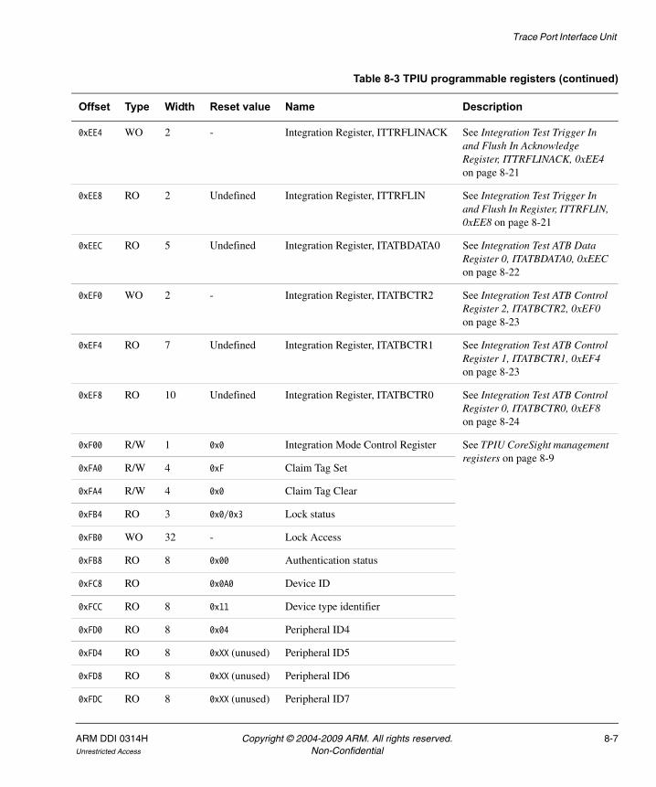
Trace Port Interface Unit
0xEE4 WO 2 - Integration Register, ITTRFLINACK See Integration Test Trigger In and Flush In Acknowledge Register, ITTRFLINACK, 0xEE4 on page 8-21
0xEE8 RO 2 Undefined Integration Register, ITTRFLIN See Integration Test Trigger In and Flush In Register, ITTRFLIN, 0xEE8 on page 8-21
0xEEC RO 5 Undefined Integration Register, ITATBDATA0 See Integration Test ATB Data Register 0, ITATBDATA0, 0xEEC on page 8-22
0xEF0 WO 2 - Integration Register, ITATBCTR2 See Integration Test ATB Control Register 2, ITATBCTR2, 0xEF0 on page 8-23
0xEF4 RO 7 Undefined Integration Register, ITATBCTR1 See Integration Test ATB Control Register 1, ITATBCTR1, 0xEF4 on page 8-23
0xEF8 RO 10 Undefined Integration Register, ITATBCTR0 See Integration Test ATB Control Register 0, ITATBCTR0, 0xEF8 on page 8-24
0xF00 R/W 1 0x0 Integration Mode Control Register See TPIU CoreSight management registers on page 8-9
0xFA0 R/W 4 0xF Claim Tag Set
0xFA4 R/W 4 0x0 Claim Tag Clear
0xFB4 RO 3 0x0/0x3 Lock status
0xFB0 WO 32 - Lock Access
0xFB8 RO 8 0x00 Authentication status
0xFC8 RO 0x0A0 Device ID
0xFCC RO 8 0x11 Device type identifier
0xFD0 RO 8 0x04 Peripheral ID4
0xFD4 RO 8 0xXX (unused) Peripheral ID5
0xFD8 RO 8 0xXX (unused) Peripheral ID6
0xFDC RO 8 0xXX (unused) Peripheral ID7
Table 8-3 TPIU programmable registers (continued)
Offset Type Width Reset value Name Description
ARM DDI 0314H Copyright © 2004-2009 ARM. All rights reserved. 8-7Unrestricted Access Non-Confidential
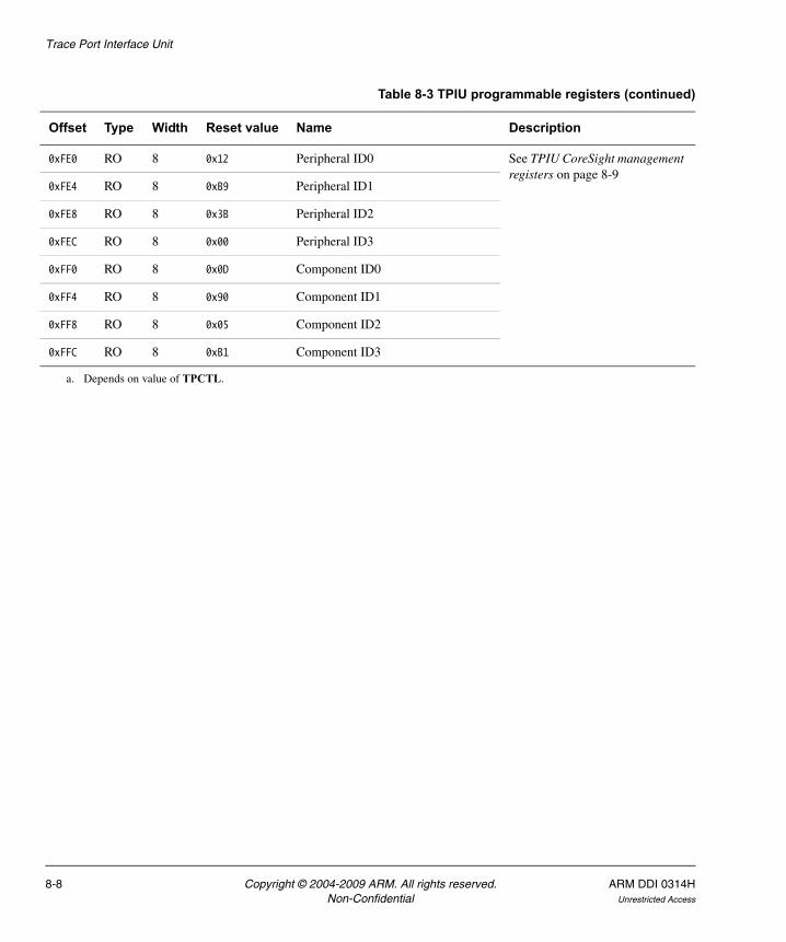
Trace Port Interface Unit
0xFE0 RO 8 0x12 Peripheral ID0 See TPIU CoreSight management registers on page 8-9
0xFE4 RO 8 0xB9 Peripheral ID1
0xFE8 RO 8 0x3B Peripheral ID2
0xFEC RO 8 0x00 Peripheral ID3
0xFF0 RO 8 0x0D Component ID0
0xFF4 RO 8 0x90 Component ID1
0xFF8 RO 8 0x05 Component ID2
0xFFC RO 8 0xB1 Component ID3
a. Depends on value of TPCTL.
Table 8-3 TPIU programmable registers (continued)
Offset Type Width Reset value Name Description
8-8 Copyright © 2004-2009 ARM. All rights reserved. ARM DDI 0314HNon-Confidential Unrestricted Access
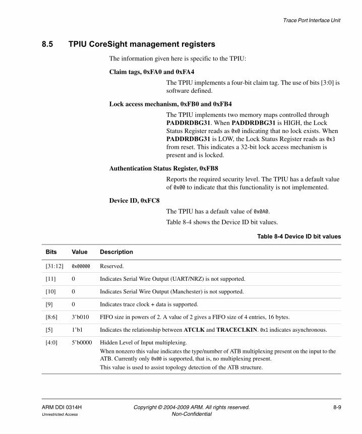
Trace Port Interface Unit
8.5 TPIU CoreSight management registersThe information given here is specific to the TPIU:
Claim tags, 0xFA0 and 0xFA4
The TPIU implements a four-bit claim tag. The use of bits [3:0] is software defined.
Lock access mechanism, 0xFB0 and 0xFB4
The TPIU implements two memory maps controlled through PADDRDBG31. When PADDRDBG31 is HIGH, the Lock Status Register reads as 0x0 indicating that no lock exists. When PADDRDBG31 is LOW, the Lock Status Register reads as 0x3 from reset. This indicates a 32-bit lock access mechanism is present and is locked.
Authentication Status Register, 0xFB8
Reports the required security level. The TPIU has a default value of 0x00 to indicate that this functionality is not implemented.
Device ID, 0xFC8
The TPIU has a default value of 0x0A0.
Table 8-4 shows the Device ID bit values.
Table 8-4 Device ID bit values
Bits Value Description
[31:12] 0x00000 Reserved.
[11] 0 Indicates Serial Wire Output (UART/NRZ) is not supported.
[10] 0 Indicates Serial Wire Output (Manchester) is not supported.
[9] 0 Indicates trace clock + data is supported.
[8:6] 3’b010 FIFO size in powers of 2. A value of 2 gives a FIFO size of 4 entries, 16 bytes.
[5] 1’b1 Indicates the relationship between ATCLK and TRACECLKIN. 0x1 indicates asynchronous.
[4:0] 5’b0000 Hidden Level of Input multiplexing.
When nonzero this value indicates the type/number of ATB multiplexing present on the input to the ATB. Currently only 0x00 is supported, that is, no multiplexing present.
This value is used to assist topology detection of the ATB structure.
ARM DDI 0314H Copyright © 2004-2009 ARM. All rights reserved. 8-9Unrestricted Access Non-Confidential
Trace Port Interface Unit
Device Type Identifier, 0xFCC
0x11 indicates this device is a trace sink (0x1) and specifically a TPIU (0x1).
Part number, 0xFE4[3:0], 0xFE0[7:4], and 0xFE0[3:0]
Upper, middle, and lower BCD value of Device number. This is set to 0x912.
Designer JEP106 value, 0xFD0[3:0], 0xFE8[2:0], 0xFE4[7:4]
The TPIU is identified as an ARM component with a JEP106 identity at 0x3B and a JEP106 continuation code at 0x4 (fifth bank).
Component class, 0xFF4[7:4]
The TPIU complies to the CoreSight class of components and this value is set to 0x9.
See Table 1-1 on page 1-4 for the current value of the revision field at offset 0xFE8[7:4].
8-10 Copyright © 2004-2009 ARM. All rights reserved. ARM DDI 0314HNon-Confidential Unrestricted Access
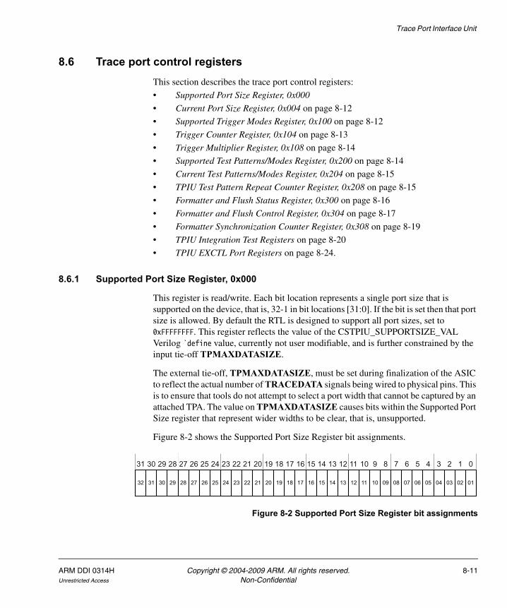
Trace Port Interface Unit
8.6 Trace port control registersThis section describes the trace port control registers:
• Supported Port Size Register, 0x000
• Current Port Size Register, 0x004 on page 8-12
• Supported Trigger Modes Register, 0x100 on page 8-12
• Trigger Counter Register, 0x104 on page 8-13
• Trigger Multiplier Register, 0x108 on page 8-14
• Supported Test Patterns/Modes Register, 0x200 on page 8-14
• Current Test Patterns/Modes Register, 0x204 on page 8-15
• TPIU Test Pattern Repeat Counter Register, 0x208 on page 8-15
• Formatter and Flush Status Register, 0x300 on page 8-16
• Formatter and Flush Control Register, 0x304 on page 8-17
• Formatter Synchronization Counter Register, 0x308 on page 8-19
• TPIU Integration Test Registers on page 8-20
• TPIU EXCTL Port Registers on page 8-24.
8.6.1 Supported Port Size Register, 0x000
This register is read/write. Each bit location represents a single port size that is supported on the device, that is, 32-1 in bit locations [31:0]. If the bit is set then that port size is allowed. By default the RTL is designed to support all port sizes, set to 0xFFFFFFFF. This register reflects the value of the CSTPIU_SUPPORTSIZE_VAL Verilog `define value, currently not user modifiable, and is further constrained by the input tie-off TPMAXDATASIZE.
The external tie-off, TPMAXDATASIZE, must be set during finalization of the ASIC to reflect the actual number of TRACEDATA signals being wired to physical pins. This is to ensure that tools do not attempt to select a port width that cannot be captured by an attached TPA. The value on TPMAXDATASIZE causes bits within the Supported Port Size register that represent wider widths to be clear, that is, unsupported.
Figure 8-2 shows the Supported Port Size Register bit assignments.
Figure 8-2 Supported Port Size Register bit assignments
32 02 01
31 30 29 28 27 26 25 24 23 22 21 20 19 18 17 16 15 14 13 12 11 10 9 8 7 6 5 4 3 2 1 0
31 30 29 28 27 26 25 24 23 22 21 20 19 18 17 16 15 14 13 12 11 10 09 08 07 06 05 04 03
ARM DDI 0314H Copyright © 2004-2009 ARM. All rights reserved. 8-11Unrestricted Access Non-Confidential
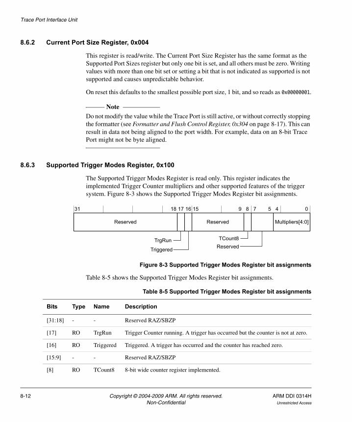
Trace Port Interface Unit
8.6.2 Current Port Size Register, 0x004
This register is read/write. The Current Port Size Register has the same format as the Supported Port Sizes register but only one bit is set, and all others must be zero. Writing values with more than one bit set or setting a bit that is not indicated as supported is not supported and causes unpredictable behavior.
On reset this defaults to the smallest possible port size, 1 bit, and so reads as 0x00000001.
Note Do not modify the value while the Trace Port is still active, or without correctly stopping the formatter (see Formatter and Flush Control Register, 0x304 on page 8-17). This can result in data not being aligned to the port width. For example, data on an 8-bit Trace Port might not be byte aligned.
8.6.3 Supported Trigger Modes Register, 0x100
The Supported Trigger Modes Register is read only. This register indicates the implemented Trigger Counter multipliers and other supported features of the trigger system. Figure 8-3 shows the Supported Trigger Modes Register bit assignments.
Figure 8-3 Supported Trigger Modes Register bit assignments
Table 8-5 shows the Supported Trigger Modes Register bit assignments.
Reserved Reserved Multipliers[4:0]
31 18 17 16 15 9 8 7 5 4 0
Triggered
TrgRun TCount8Reserved
Table 8-5 Supported Trigger Modes Register bit assignments
Bits Type Name Description
[31:18] - - Reserved RAZ/SBZP
[17] RO TrgRun Trigger Counter running. A trigger has occurred but the counter is not at zero.
[16] RO Triggered Triggered. A trigger has occurred and the counter has reached zero.
[15:9] - - Reserved RAZ/SBZP
[8] RO TCount8 8-bit wide counter register implemented.
8-12 Copyright © 2004-2009 ARM. All rights reserved. ARM DDI 0314HNon-Confidential Unrestricted Access
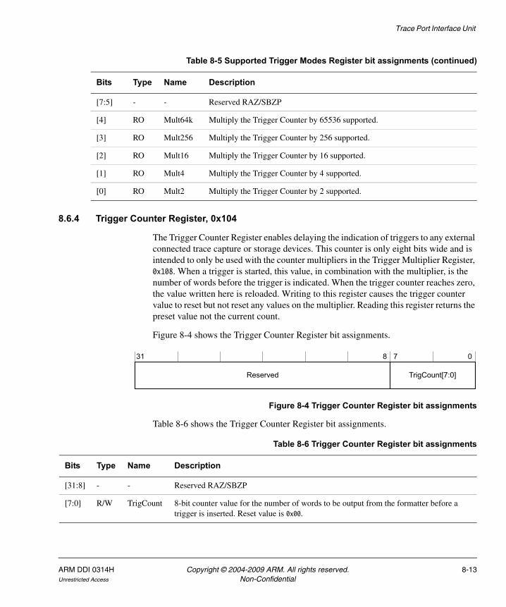
Trace Port Interface Unit
8.6.4 Trigger Counter Register, 0x104
The Trigger Counter Register enables delaying the indication of triggers to any external connected trace capture or storage devices. This counter is only eight bits wide and is intended to only be used with the counter multipliers in the Trigger Multiplier Register, 0x108. When a trigger is started, this value, in combination with the multiplier, is the number of words before the trigger is indicated. When the trigger counter reaches zero, the value written here is reloaded. Writing to this register causes the trigger counter value to reset but not reset any values on the multiplier. Reading this register returns the preset value not the current count.
Figure 8-4 shows the Trigger Counter Register bit assignments.
Figure 8-4 Trigger Counter Register bit assignments
Table 8-6 shows the Trigger Counter Register bit assignments.
[7:5] - - Reserved RAZ/SBZP
[4] RO Mult64k Multiply the Trigger Counter by 65536 supported.
[3] RO Mult256 Multiply the Trigger Counter by 256 supported.
[2] RO Mult16 Multiply the Trigger Counter by 16 supported.
[1] RO Mult4 Multiply the Trigger Counter by 4 supported.
[0] RO Mult2 Multiply the Trigger Counter by 2 supported.
Table 8-5 Supported Trigger Modes Register bit assignments (continued)
Bits Type Name Description
TrigCount[7:0]Reserved
31 8 7 0
Table 8-6 Trigger Counter Register bit assignments
Bits Type Name Description
[31:8] - - Reserved RAZ/SBZP
[7:0] R/W TrigCount 8-bit counter value for the number of words to be output from the formatter before a trigger is inserted. Reset value is 0x00.
ARM DDI 0314H Copyright © 2004-2009 ARM. All rights reserved. 8-13Unrestricted Access Non-Confidential
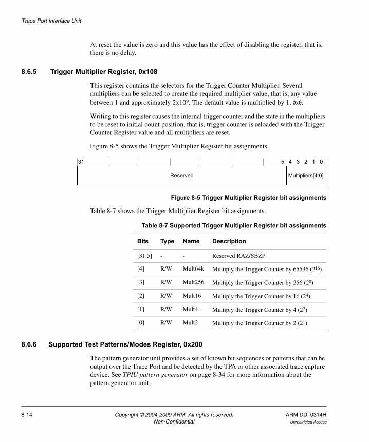
Trace Port Interface Unit
At reset the value is zero and this value has the effect of disabling the register, that is, there is no delay.
8.6.5 Trigger Multiplier Register, 0x108
This register contains the selectors for the Trigger Counter Multiplier. Several multipliers can be selected to create the required multiplier value, that is, any value between 1 and approximately 2x10⁹. The default value is multiplied by 1, 0x0.
Writing to this register causes the internal trigger counter and the state in the multipliers to be reset to initial count position, that is, trigger counter is reloaded with the Trigger Counter Register value and all multipliers are reset.
Figure 8-5 shows the Trigger Multiplier Register bit assignments.
Figure 8-5 Trigger Multiplier Register bit assignments
Table 8-7 shows the Trigger Multiplier Register bit assignments.
8.6.6 Supported Test Patterns/Modes Register, 0x200
The pattern generator unit provides a set of known bit sequences or patterns that can be output over the Trace Port and be detected by the TPA or other associated trace capture device. See TPIU pattern generator on page 8-34 for more information about the pattern generator unit.
Multipliers[4:0]Reserved
31 5 4 3 2 1 0
Table 8-7 Supported Trigger Multiplier Register bit assignments
Bits Type Name Description
[31:5] - - Reserved RAZ/SBZP
[4] R/W Mult64k Multiply the Trigger Counter by 65536 (216)
[3] R/W Mult256 Multiply the Trigger Counter by 256 (28)
[2] R/W Mult16 Multiply the Trigger Counter by 16 (24)
[1] R/W Mult4 Multiply the Trigger Counter by 4 (22)
[0] R/W Mult2 Multiply the Trigger Counter by 2 (21)
8-14 Copyright © 2004-2009 ARM. All rights reserved. ARM DDI 0314HNon-Confidential Unrestricted Access
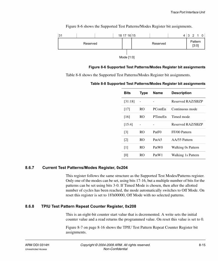
Trace Port Interface Unit
Figure 8-6 shows the Supported Test Patterns/Modes Register bit assignments.
Figure 8-6 Supported Test Patterns/Modes Register bit assignments
Table 8-8 shows the Supported Test Patterns/Modes Register bit assignments.
8.6.7 Current Test Patterns/Modes Register, 0x204
This register follows the same structure as the Supported Test Modes/Patterns register. Only one of the modes can be set, using bits 17-16, but a multiple number of bits for the patterns can be set using bits 3-0. If Timed Mode is chosen, then after the allotted number of cycles has been reached, the mode automatically switches to Off Mode. On reset this register is set to 18'h00000, Off Mode with no selected patterns.
8.6.8 TPIU Test Pattern Repeat Counter Register, 0x208
This is an eight-bit counter start value that is decremented. A write sets the initial counter value and a read returns the programmed value. On reset this value is set to 0.
Figure 8-7 on page 8-16 shows the TPIU Test Pattern Repeat Counter Register bit assignments.
ReservedReserved Pattern[3:0]
31 18 17 16 15 4 3 2 1 0
Mode [1:0]
Table 8-8 Supported Test Patterns/Modes Register bit assignments
Bits Type Name Description
[31:18] - - Reserved RAZ/SBZP
[17] RO PContEn Continuous mode
[16] RO PTimeEn Timed mode
[15:4] - - Reserved RAZ/SBZP
[3] RO PatF0 FF/00 Pattern
[2] RO PatA5 AA/55 Pattern
[1] RO PatW0 Walking 0s Pattern
[0] RO PatW1 Walking 1s Pattern
ARM DDI 0314H Copyright © 2004-2009 ARM. All rights reserved. 8-15Unrestricted Access Non-Confidential
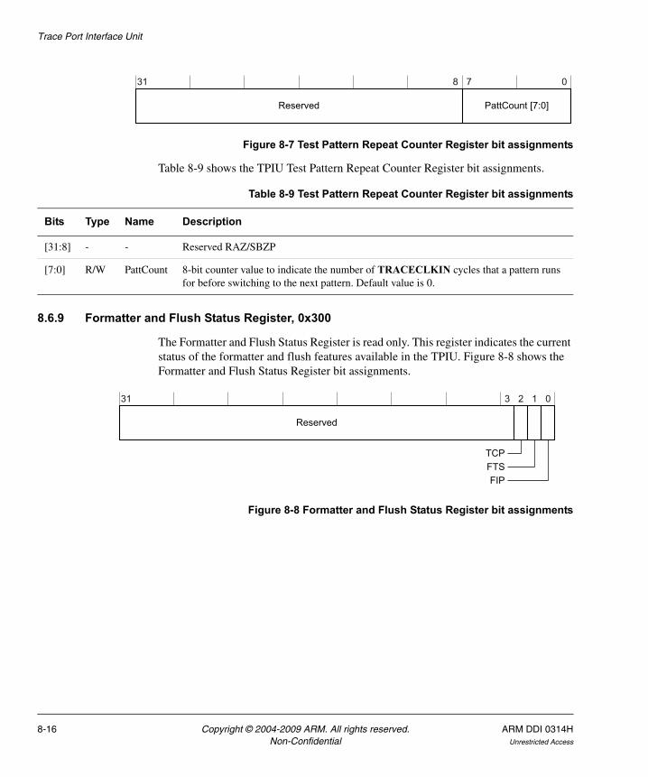
Trace Port Interface Unit
Figure 8-7 Test Pattern Repeat Counter Register bit assignments
Table 8-9 shows the TPIU Test Pattern Repeat Counter Register bit assignments.
8.6.9 Formatter and Flush Status Register, 0x300
The Formatter and Flush Status Register is read only. This register indicates the current status of the formatter and flush features available in the TPIU. Figure 8-8 shows the Formatter and Flush Status Register bit assignments.
Figure 8-8 Formatter and Flush Status Register bit assignments
Reserved PattCount [7:0]
31 8 7 0
Table 8-9 Test Pattern Repeat Counter Register bit assignments
Bits Type Name Description
[31:8] - - Reserved RAZ/SBZP
[7:0] R/W PattCount 8-bit counter value to indicate the number of TRACECLKIN cycles that a pattern runs for before switching to the next pattern. Default value is 0.
Reserved
TCPFTSFIP
31 3 2 1 0
8-16 Copyright © 2004-2009 ARM. All rights reserved. ARM DDI 0314HNon-Confidential Unrestricted Access
Trace Port Interface Unit
Table 8-10 shows the Formatter and Flush Status Register bit assignments.
8.6.10 Formatter and Flush Control Register, 0x304
This register controls the generation of stop, trigger, and flush events. Figure 8-9 shows the Formatter and Flush Control Register bit assignments.
Figure 8-9 Formatter and Flush Control Register bit assignments
Table 8-10 Formatter and Flush Status Register bit assignments
Bits Type Name Description
[31:3] - - Reserved RAZ/SBZP.
[2] RO TCPresent If this bit is set then TRACECTL is present. If no TRACECTL pin is available, that is, this bit is zero, then the data formatter must be used and only in continuous mode.
This is constrained by the CSTPIU_TRACECTL_VAL Verilog ̀ define, which is not user modifiable, and the external tie-off TPCTL. If either constraint reports zero/LOW then no TRACECTL is present and this inability to use the pin is reflected in this register. See TRACECTL removal on page 8-31 for more information.
[1] RO FtStopped Formatter stopped. The formatter has received a stop request signal and all trace data and post-amble has been output. Any more trace data on the ATB interface is ignored and ATREADYS goes HIGH.
[0] RO FlInProg Flush In Progress. This is an indication of the current state of AFVALIDS.
Reserved
31 14 13 12 11 10 9 8 7 6 5 4 3 2 1 0
Reserved
Reserved
TrigFlTrigEvt
TrigIn
FOnManFOnTrigFOnFlIn
StopTrigStopFl
ReservedEnFCont
EnFTCEnF events
Trigger marks
FOn events
Stop events
15
ARM DDI 0314H Copyright © 2004-2009 ARM. All rights reserved. 8-17Unrestricted Access Non-Confidential
Trace Port Interface Unit
Table 8-11 shows the Formatter and Flush Control Register bit assignments.
To disable formatting and put the formatter into bypass mode, bits 1 and 0 must be clear. Setting both bits is the same as setting bit 1.
Table 8-11 Formatter and Flush Control Register bit assignments
Bits Type Name Description
[31:14] - - Reserved RAZ/SBZP.
[13] R/W StopTrig Stop the formatter after a Trigger Eventa is observed. Reset to disabled, or zero.
[12] R/W StopFl Stop the formatter after a flush completes (return of AFREADYS). This forces the FIFO to drain off any part-completed packets. Setting this bit enables this function but this is clear on reset, or disabled.
[11] - - Reserved RAZ/SBZP.
[10] R/W TrigFl Indicates a trigger on Flush completion on AFREADYS being returned.
[9] R/W TrigEvt Indicate a trigger on a Trigger Eventa.
[8] R/W TrigIn Indicate a trigger on TRIGIN being asserted.
[7] - - Reserved RAZ/SBZP.
[6] R/W FOnMan Manually generate a flush of the system. Setting this bit causes a flush to be generated. This is cleared when this flush has been serviced. This bit is clear on reset.
[5] R/W FOnTrig Generate flush using Trigger event. Set this bit to cause a flush of data in the system when a Trigger Eventa occurs. Reset value is this bit clear.
[4] R/W FOnFlIn Generate flush using the FLUSHIN interface. Set this bit to enable use of the FLUSHIN connection. This is clear on reset.
[3:2] - - Reserved RAZ/SBZP.
[1] R/W EnFCont Continuous Formatting, no TRACECTL. Embed in trigger packets and indicate null cycles using Sync packets. Reset value is this bit clear. Can only be changed when FtStopped is HIGH.
[0] R/W EnFTC Enable Formatting. Do not embed Triggers into the formatted stream. Trace disable cycles and triggers are indicated by TRACECTL, where fitted. Reset value is this bit clear. Can only be changed when FtStopped is HIGH.
a. A Trigger Event is defined as when the Trigger counter reaches zero or, in the case of the Trigger counter being zero, when TRIGIN is HIGH.
8-18 Copyright © 2004-2009 ARM. All rights reserved. ARM DDI 0314HNon-Confidential Unrestricted Access
Trace Port Interface Unit
All three flush generating conditions can be enabled together. However, if a second or third flush event is generated from another condition then the current flush completes before the next flush is serviced. Flush from FLUSHIN takes priority over flush from Trigger, which in turn completes before a manually activated flush. All Trigger indication conditions can be enabled simultaneously although this can cause the appearance of multiple triggers if flush using trigger is also enabled.
Both 'Stop On' settings can be enabled, although if flush on trigger is set up then none of the flushed data is stored. When the system stops, it returns ATREADYS and does not store the accepted data packets. This is to avoid stalling of any other devices that are connected to a Trace Replicator.
If an event in the Formatter and Flush Control Register is required, it must be enabled before the originating event starts. Because requests from flushes and triggers can originate in an asynchronous clock domain, the exact time the component acts on the request cannot be determined with respect to configuring the control.
Note • It is recommended that the Trace Port width is changed without enabling
continuous mode. Enabling continuous mode causes data to be output from the Trace Port and modifying the port size can result in data not being aligned for power2 port widths.
• To perform a stop on flush completion through a manually-generated flush request, two write operations to the register are required:
— one to enable the stop event, if it is not already enabled
— one to generate the manual flush.
8.6.11 Formatter Synchronization Counter Register, 0x308
The Formatter Synchronization Counter Register enables effective use on different sized Trace Port Analyzers (TPAs) without wasting large amounts of the storage capacity of the capture device.
This counter is the number of formatter frames since the last synchronization packet of 128 bits, and is a 12-bit counter with a maximum count value of 4096. This equates to synchronization every 65536 bytes, that is, 4096 packets x 16 bytes per packet. The default is set up for a synchronization packet every 1024 bytes, that is, every 64 formatter frames.
Figure 8-10 on page 8-20 shows the Formatter Synchronization Counter Register bit assignments.
ARM DDI 0314H Copyright © 2004-2009 ARM. All rights reserved. 8-19Unrestricted Access Non-Confidential
Trace Port Interface Unit
Figure 8-10 Formatter Synchronization Counter Register bit assignments
Table 8-12 shows the Formatter Synchronization Counter Register bit assignments.
If the formatter has been configured for continuous mode, full and half-word sync frames are inserted during normal operation. Under these circumstances the count value represents the maximum number of complete frames between full synchronization packets.
See Supported Trigger Modes Register, 0x100 on page 8-12 for more on different modes.
8.6.12 TPIU Integration Test Registers
Integration Test Registers are provided to simplify the process of verifying the integration of the TPIU with other devices in a CoreSight system. These registers enable direct control of outputs and the ability to read the value of inputs. You must only use these registers when the Integration Mode Control Register (0xF00) bit [0] is set to 1.
The registers in the TPIU enable the system to set the FLUSHINACK and TRIGINACK output pins. The FLUSHIN and TRIGIN inputs to the TPIU can also be read. The other Integration Test Registers are for testing the integration of the ATB slave interface on the TPIU. For details of how to use these signals see the applicable CoreSight DK Integration Manual.
This section describes the following registers:
• Integration Test Trigger In and Flush In Acknowledge Register, ITTRFLINACK, 0xEE4 on page 8-21
• Integration Test Trigger In and Flush In Register, ITTRFLIN, 0xEE8 on page 8-21
• Integration Test ATB Data Register 0, ITATBDATA0, 0xEEC on page 8-22
• Integration Test ATB Control Register 2, ITATBCTR2, 0xEF0 on page 8-23
Reserved CycCount [11:0]
31 12 11 0
Table 8-12 Formatter Synchronization Counter Register bit assignments
Bits Type Name Description
[31:12] - - Reserved RAZ/SBZP.
[11:0] R/W CycCount 12-bit counter value to indicate the number of complete frames between full synchronization packets. Default value is 64 (0x40).
8-20 Copyright © 2004-2009 ARM. All rights reserved. ARM DDI 0314HNon-Confidential Unrestricted Access
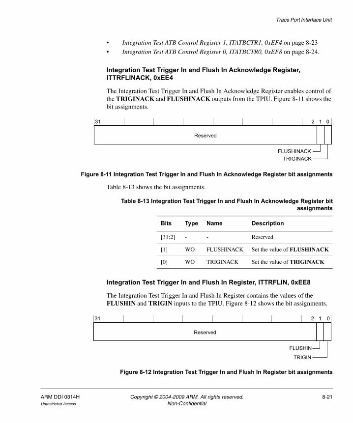
Trace Port Interface Unit
• Integration Test ATB Control Register 1, ITATBCTR1, 0xEF4 on page 8-23
• Integration Test ATB Control Register 0, ITATBCTR0, 0xEF8 on page 8-24.
Integration Test Trigger In and Flush In Acknowledge Register, ITTRFLINACK, 0xEE4
The Integration Test Trigger In and Flush In Acknowledge Register enables control of the TRIGINACK and FLUSHINACK outputs from the TPIU. Figure 8-11 shows the bit assignments.
Figure 8-11 Integration Test Trigger In and Flush In Acknowledge Register bit assignments
Table 8-13 shows the bit assignments.
Integration Test Trigger In and Flush In Register, ITTRFLIN, 0xEE8
The Integration Test Trigger In and Flush In Register contains the values of the FLUSHIN and TRIGIN inputs to the TPIU. Figure 8-12 shows the bit assignments.
Figure 8-12 Integration Test Trigger In and Flush In Register bit assignments
31 2 1 0
FLUSHINACKTRIGINACK
Reserved
Table 8-13 Integration Test Trigger In and Flush In Acknowledge Register bitassignments
Bits Type Name Description
[31:2] - - Reserved
[1] WO FLUSHINACK Set the value of FLUSHINACK
[0] WO TRIGINACK Set the value of TRIGINACK
31 2 1 0
FLUSHIN
TRIGIN
Reserved
ARM DDI 0314H Copyright © 2004-2009 ARM. All rights reserved. 8-21Unrestricted Access Non-Confidential
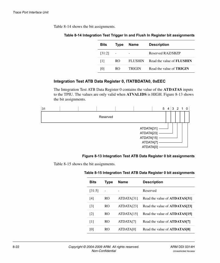
Trace Port Interface Unit
Table 8-14 shows the bit assignments.
Integration Test ATB Data Register 0, ITATBDATA0, 0xEEC
The Integration Test ATB Data Register 0 contains the value of the ATDATAS inputs to the TPIU. The values are only valid when ATVALIDS is HIGH. Figure 8-13 shows the bit assignments.
Figure 8-13 Integration Test ATB Data Register 0 bit assignments
Table 8-15 shows the bit assignments.
Table 8-14 Integration Test Trigger In and Flush In Register bit assignments
Bits Type Name Description
[31:2] - - Reserved RAZ/SBZP
[1] RO FLUSHIN Read the value of FLUSHIN
[0] RO TRIGIN Read the value of TRIGIN
31 4 3 2 1
Reserved
0
ATDATA[31]ATDATA[23]ATDATA[15]
ATDATA[0]ATDATA[7]
5
Table 8-15 Integration Test ATB Data Register 0 bit assignments
Bits Type Name Description
[31:5] - - Reserved
[4] RO ATDATA[31] Read the value of ATDATAS[31]
[3] RO ATDATA[23] Read the value of ATDATAS[23]
[2] RO ATDATA[15] Read the value of ATDATAS[15]
[1] RO ATDATA[7] Read the value of ATDATAS[7]
[0] RO ATDATA[0] Read the value of ATDATAS[0]
8-22 Copyright © 2004-2009 ARM. All rights reserved. ARM DDI 0314HNon-Confidential Unrestricted Access
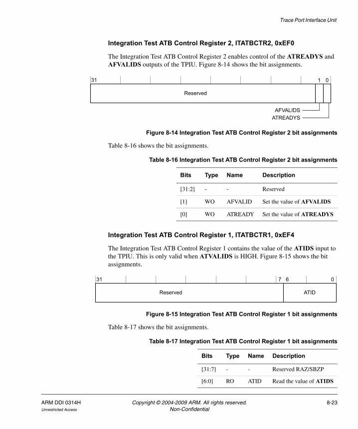
Trace Port Interface Unit
Integration Test ATB Control Register 2, ITATBCTR2, 0xEF0
The Integration Test ATB Control Register 2 enables control of the ATREADYS and AFVALIDS outputs of the TPIU. Figure 8-14 shows the bit assignments.
Figure 8-14 Integration Test ATB Control Register 2 bit assignments
Table 8-16 shows the bit assignments.
Integration Test ATB Control Register 1, ITATBCTR1, 0xEF4
The Integration Test ATB Control Register 1 contains the value of the ATIDS input to the TPIU. This is only valid when ATVALIDS is HIGH. Figure 8-15 shows the bit assignments.
Figure 8-15 Integration Test ATB Control Register 1 bit assignments
Table 8-17 shows the bit assignments.
31
Reserved
01
AFVALIDSATREADYS
Table 8-16 Integration Test ATB Control Register 2 bit assignments
Bits Type Name Description
[31:2] - - Reserved
[1] WO AFVALID Set the value of AFVALIDS
[0] WO ATREADY Set the value of ATREADYS
31
Reserved
6 0
ATID
7
Table 8-17 Integration Test ATB Control Register 1 bit assignments
Bits Type Name Description
[31:7] - - Reserved RAZ/SBZP
[6:0] RO ATID Read the value of ATIDS
ARM DDI 0314H Copyright © 2004-2009 ARM. All rights reserved. 8-23Unrestricted Access Non-Confidential
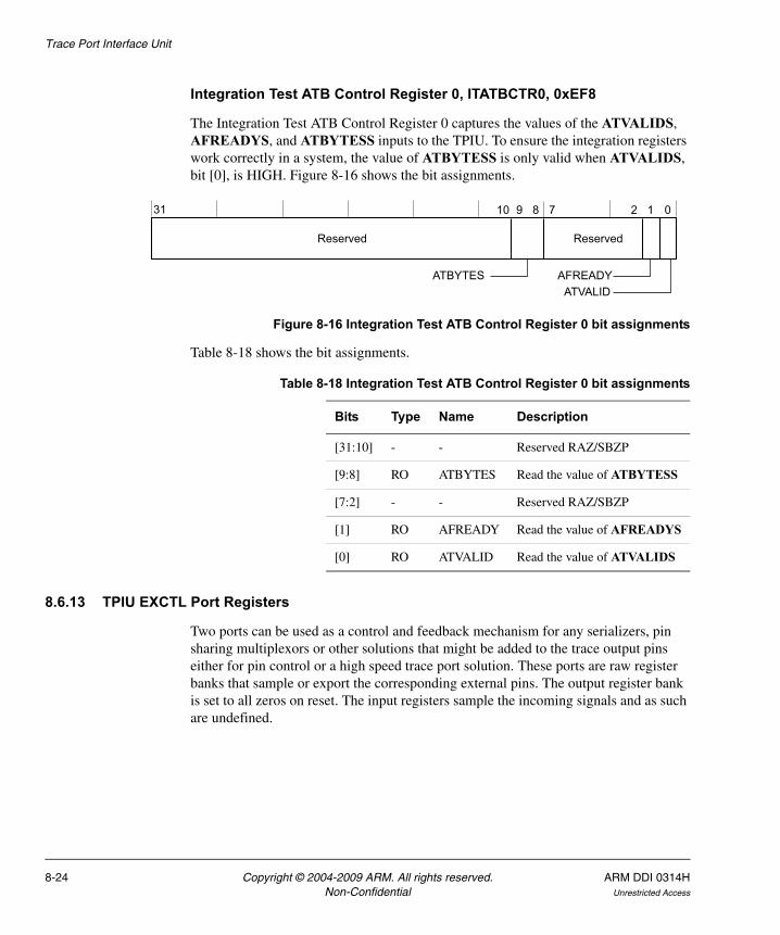
Trace Port Interface Unit
Integration Test ATB Control Register 0, ITATBCTR0, 0xEF8
The Integration Test ATB Control Register 0 captures the values of the ATVALIDS, AFREADYS, and ATBYTESS inputs to the TPIU. To ensure the integration registers work correctly in a system, the value of ATBYTESS is only valid when ATVALIDS, bit [0], is HIGH. Figure 8-16 shows the bit assignments.
Figure 8-16 Integration Test ATB Control Register 0 bit assignments
Table 8-18 shows the bit assignments.
8.6.13 TPIU EXCTL Port Registers
Two ports can be used as a control and feedback mechanism for any serializers, pin sharing multiplexors or other solutions that might be added to the trace output pins either for pin control or a high speed trace port solution. These ports are raw register banks that sample or export the corresponding external pins. The output register bank is set to all zeros on reset. The input registers sample the incoming signals and as such are undefined.
31
Reserved
01
AFREADYATVALID
9 8
Reserved
ATBYTES
10 7 2
Table 8-18 Integration Test ATB Control Register 0 bit assignments
Bits Type Name Description
[31:10] - - Reserved RAZ/SBZP
[9:8] RO ATBYTES Read the value of ATBYTESS
[7:2] - - Reserved RAZ/SBZP
[1] RO AFREADY Read the value of AFREADYS
[0] RO ATVALID Read the value of ATVALIDS
8-24 Copyright © 2004-2009 ARM. All rights reserved. ARM DDI 0314HNon-Confidential Unrestricted Access
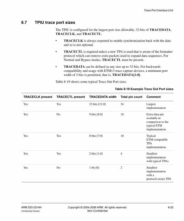
Trace Port Interface Unit
8.7 TPIU trace port sizesThe TPIU is configured for the largest port size allowable, 32 bits of TRACEDATA, TRACECLK, and TRACECTL.
• TRACECLK is always exported to enable synchronization back with the data and so is not optional.
• TRACECTL is required unless a new TPA is used that is aware of the formatter protocol which can remove extra packets used to expand data sequences. For Normal and Bypass modes, TRACECTL must be present.
• TRACEDATA can be defined as any size up to 32 bits. For backwards compatibility and usage with ETMv3 trace capture devices, a minimum port width of 2 bits is permitted, that is, TRACEDATA[1:0].
Table 8-19 shows some typical Trace Out Port sizes.
Table 8-19 Example Trace Out Port sizes
TRACECLK present TRACECTL present TRACEDATA width Total pin count Comment
Yes Yes 32 bits [31:0] 34 Largest implementation
Yes No 9 bits [8:0] 10 Extra data pin available in comparison to the typical ETM implementation.
Yes Yes 8 bits [7:0] 10 Typical ETM-compatible TPA implementation.
Yes Yes 2 bits [1:0] 4 Smallest implementation with typical TPAs.
Yes No 1 bit [0] 2 Smallest implementation with a protocol-aware TPA
ARM DDI 0314H Copyright © 2004-2009 ARM. All rights reserved. 8-25Unrestricted Access Non-Confidential
Trace Port Interface Unit
8.7.1 Programming registers
There are two registers that contain information relating to the physical Trace Out port. These are the Supported Port Size Register and the Formatter and Flush Status Register. For more information about these registers see Supported Port Size Register, 0x000 on page 8-11 and Formatter and Flush Control Register, 0x304 on page 8-17.
Constraining the supported TRACEDATA port widths
The TPIU currently supports data port widths from 1-32 bits. A Verilog `define, CSTPIU_SUPPORTSIZE_VAL, is used to state the supported port sizes by the RTL. This is currently set to report that all options are supported and is not user modifiable.
When placing on an Application Specific Integrated Circuit (ASIC), not all the signals of TRACEDATA can go to pads, that is, only TRACEDATA[(MDS-1):0] go to pins, where MDS represents the Maximum Data Size going to pins. If MDS is not 32, that is, the maximum supported data width for capture by a TPA is less than 32 bits of data, this must be reflected in the programmers view of the Supported Port Size Register through the tie-off input TPMAXDATASIZE[4:0]. See Supported Port Size Register, 0x000 on page 8-11 for more details.
The tie-off must be set to represent the number of TRACEDATA connections that go to ASIC pads, with all LOW indicating 1 pin, which is the minimum possible, and all HIGH indicating 32 pins, which is a full TRACEDATA bus. For example, if a 16-bit trace port is implemented, that is TRACEDATA[15:0] is connected, then TPMAXDATASIZE[4:0] must be tied to 0x0F. With a maximum TRACEDATA[7:0] connected to the ASIC, the tie-offs must be set to 0x07.
8.7.2 Omission of TRACECTL
For restricted pin devices where removal of the trace data is important, the TRACECTL can be removed. Omitting TRACECTL is only possible with the formatter enabled and continuous mode selected. See Formatter and Flush Control Register, 0x304 on page 8-17.
There are two mechanisms that can report the omission or presence of the TRACECTL pin:
• A Verilog `define, CSTPIU_TRACECTL_VAL, in the RTL that can be set to zero. This is not user-modifiable.
• An external tie-off, TPCTL, that must be tied LOW if no TRACECTL is present.
Currently, only the changing of TPCTL is supported and this must be done within the ASIC to indicate the presence, tied HIGH, or absence, tied LOW, of a TRACECTL pin.
8-26 Copyright © 2004-2009 ARM. All rights reserved. ARM DDI 0314HNon-Confidential Unrestricted Access
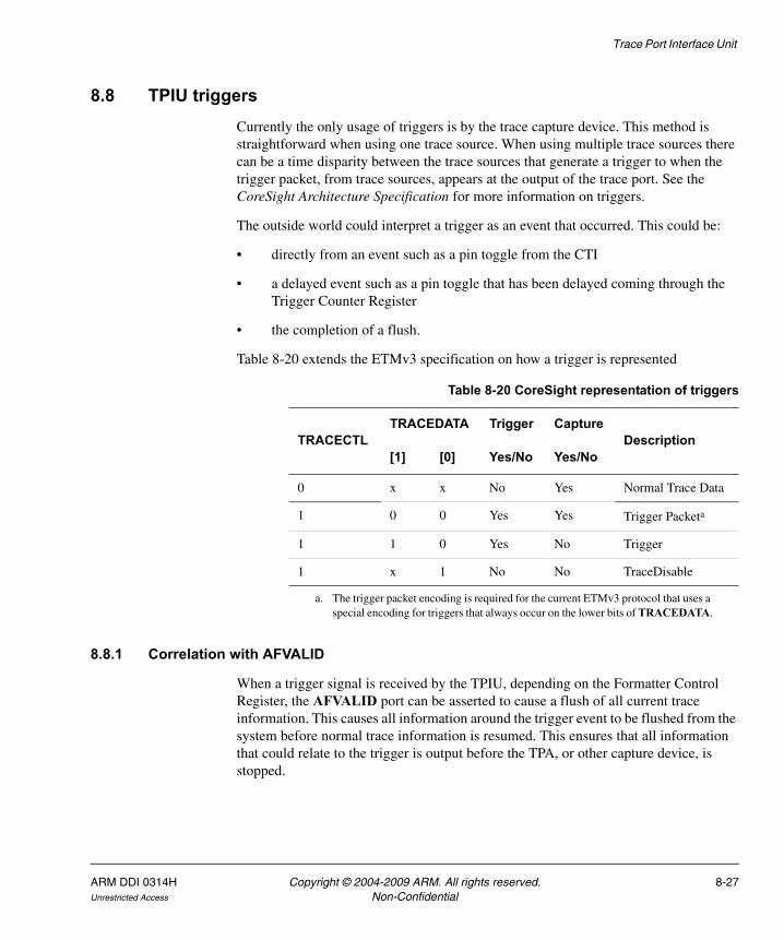
Trace Port Interface Unit
8.8 TPIU triggersCurrently the only usage of triggers is by the trace capture device. This method is straightforward when using one trace source. When using multiple trace sources there can be a time disparity between the trace sources that generate a trigger to when the trigger packet, from trace sources, appears at the output of the trace port. See the CoreSight Architecture Specification for more information on triggers.
The outside world could interpret a trigger as an event that occurred. This could be:
• directly from an event such as a pin toggle from the CTI
• a delayed event such as a pin toggle that has been delayed coming through the Trigger Counter Register
• the completion of a flush.
Table 8-20 extends the ETMv3 specification on how a trigger is represented
8.8.1 Correlation with AFVALID
When a trigger signal is received by the TPIU, depending on the Formatter Control Register, the AFVALID port can be asserted to cause a flush of all current trace information. This causes all information around the trigger event to be flushed from the system before normal trace information is resumed. This ensures that all information that could relate to the trigger is output before the TPA, or other capture device, is stopped.
Table 8-20 CoreSight representation of triggers
TRACECTLTRACEDATA Trigger Capture
Description[1] [0] Yes/No Yes/No
0 x x No Yes Normal Trace Data
1 0 0 Yes Yes Trigger Packeta
a. The trigger packet encoding is required for the current ETMv3 protocol that uses a special encoding for triggers that always occur on the lower bits of TRACEDATA.
1 1 0 Yes No Trigger
1 x 1 No No TraceDisable
ARM DDI 0314H Copyright © 2004-2009 ARM. All rights reserved. 8-27Unrestricted Access Non-Confidential
Trace Port Interface Unit
Using FOnTrig HIGH, it is possible to indicate the trigger on completion of the flush routine, so ensuring that if the TPA stopped capture on a trigger, the TPA does get all historical data relating to the trigger. See Formatter and Flush Control Register, 0x304 on page 8-17.
8-28 Copyright © 2004-2009 ARM. All rights reserved. ARM DDI 0314HNon-Confidential Unrestricted Access
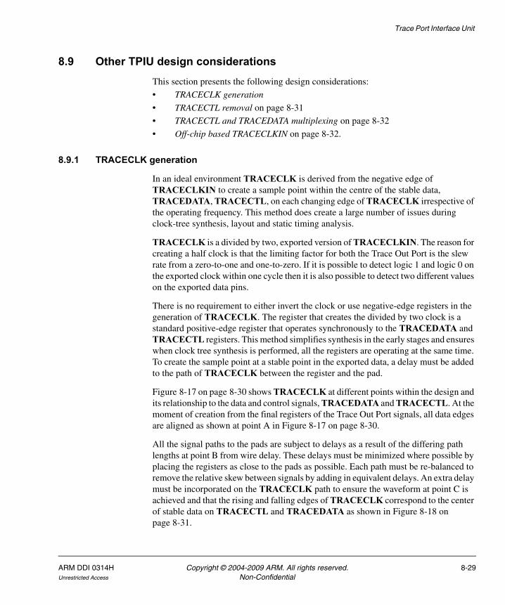
Trace Port Interface Unit
8.9 Other TPIU design considerationsThis section presents the following design considerations:
• TRACECLK generation
• TRACECTL removal on page 8-31
• TRACECTL and TRACEDATA multiplexing on page 8-32
• Off-chip based TRACECLKIN on page 8-32.
8.9.1 TRACECLK generation
In an ideal environment TRACECLK is derived from the negative edge of TRACECLKIN to create a sample point within the centre of the stable data, TRACEDATA, TRACECTL, on each changing edge of TRACECLK irrespective of the operating frequency. This method does create a large number of issues during clock-tree synthesis, layout and static timing analysis.
TRACECLK is a divided by two, exported version of TRACECLKIN. The reason for creating a half clock is that the limiting factor for both the Trace Out Port is the slew rate from a zero-to-one and one-to-zero. If it is possible to detect logic 1 and logic 0 on the exported clock within one cycle then it is also possible to detect two different values on the exported data pins.
There is no requirement to either invert the clock or use negative-edge registers in the generation of TRACECLK. The register that creates the divided by two clock is a standard positive-edge register that operates synchronously to the TRACEDATA and TRACECTL registers. This method simplifies synthesis in the early stages and ensures when clock tree synthesis is performed, all the registers are operating at the same time. To create the sample point at a stable point in the exported data, a delay must be added to the path of TRACECLK between the register and the pad.
Figure 8-17 on page 8-30 shows TRACECLK at different points within the design and its relationship to the data and control signals, TRACEDATA and TRACECTL. At the moment of creation from the final registers of the Trace Out Port signals, all data edges are aligned as shown at point A in Figure 8-17 on page 8-30.
All the signal paths to the pads are subject to delays as a result of the differing path lengths at point B from wire delay. These delays must be minimized where possible by placing the registers as close to the pads as possible. Each path must be re-balanced to remove the relative skew between signals by adding in equivalent delays. An extra delay must be incorporated on the TRACECLK path to ensure the waveform at point C is achieved and that the rising and falling edges of TRACECLK correspond to the center of stable data on TRACECTL and TRACEDATA as shown in Figure 8-18 on page 8-31.
ARM DDI 0314H Copyright © 2004-2009 ARM. All rights reserved. 8-29Unrestricted Access Non-Confidential
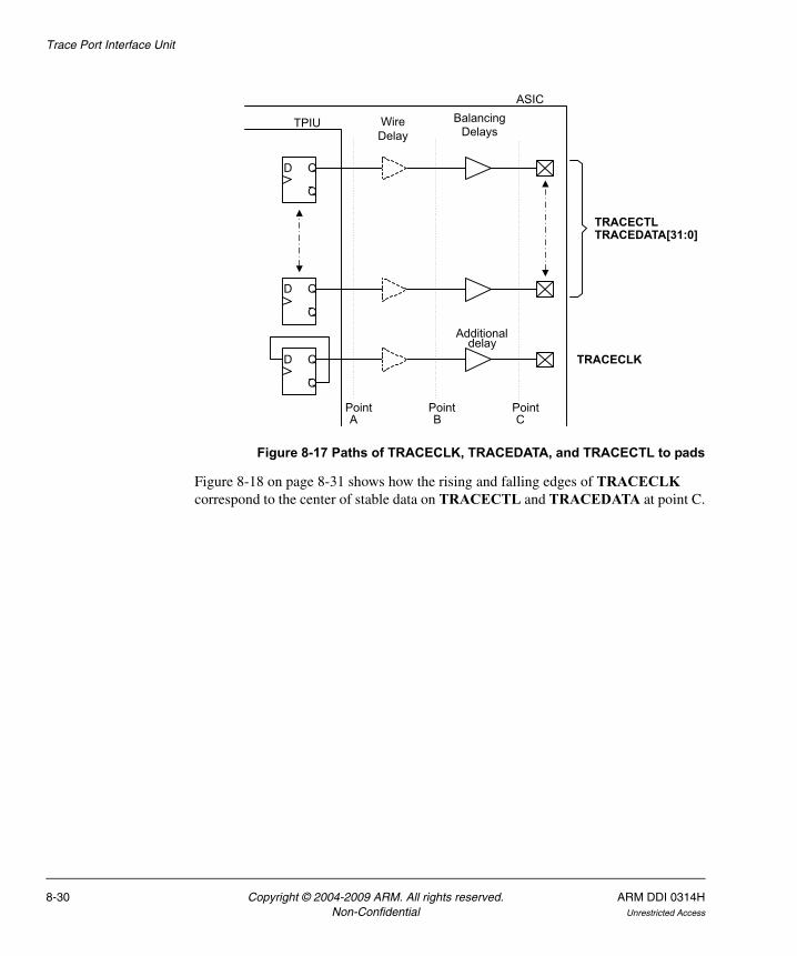
Trace Port Interface Unit
Figure 8-17 Paths of TRACECLK, TRACEDATA, and TRACECTL to pads
Figure 8-18 on page 8-31 shows how the rising and falling edges of TRACECLK correspond to the center of stable data on TRACECTL and TRACEDATA at point C.
TRACEDATA[31:0]
BalancingDelays
Wire Delay
ASIC
TPIU
D Q
Q
D Q
Q
D Q
Q
PointA
TRACECLK
TRACECTL
PointB
PointC
Additionaldelay
8-30 Copyright © 2004-2009 ARM. All rights reserved. ARM DDI 0314HNon-Confidential Unrestricted Access
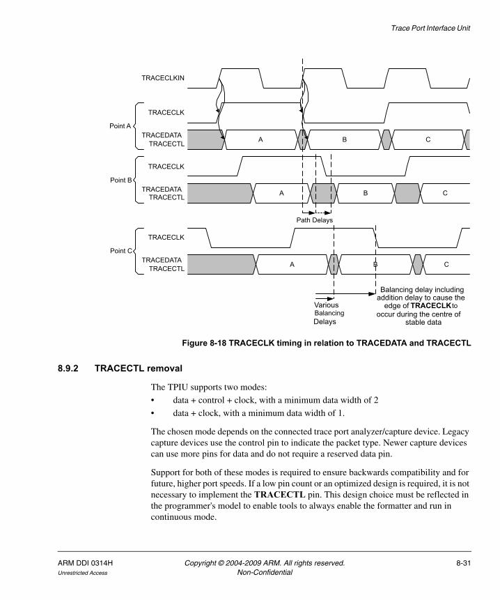
Trace Port Interface Unit
Figure 8-18 TRACECLK timing in relation to TRACEDATA and TRACECTL
8.9.2 TRACECTL removal
The TPIU supports two modes:
• data + control + clock, with a minimum data width of 2
• data + clock, with a minimum data width of 1.
The chosen mode depends on the connected trace port analyzer/capture device. Legacy capture devices use the control pin to indicate the packet type. Newer capture devices can use more pins for data and do not require a reserved data pin.
Support for both of these modes is required to ensure backwards compatibility and for future, higher port speeds. If a low pin count or an optimized design is required, it is not necessary to implement the TRACECTL pin. This design choice must be reflected in the programmer's model to enable tools to always enable the formatter and run in continuous mode.
A B CTRACEDATATRACECTL
TRACECLK
Point A
TRACECLKIN
TRACEDATATRACECTL
TRACECLK
A B C
Point C
TRACEDATATRACECTL
TRACECLK
A B C
Point B
Path Delays
VariousBalancingDelays
Balancing delay includingaddition delay to cause the
edge of TRACECLK tooccur during the centre of
stable data
ARM DDI 0314H Copyright © 2004-2009 ARM. All rights reserved. 8-31Unrestricted Access Non-Confidential
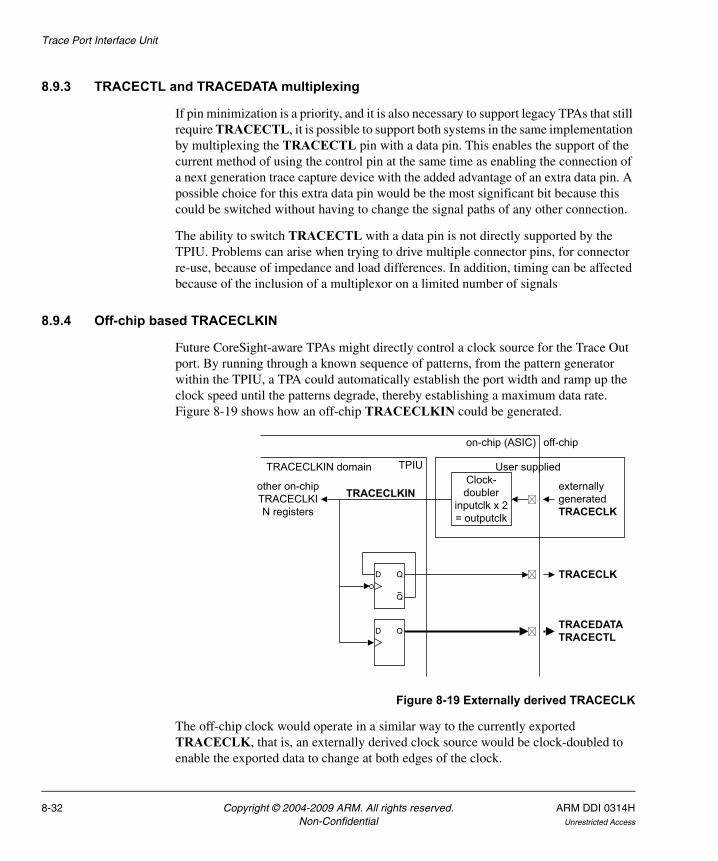
Trace Port Interface Unit
8.9.3 TRACECTL and TRACEDATA multiplexing
If pin minimization is a priority, and it is also necessary to support legacy TPAs that still require TRACECTL, it is possible to support both systems in the same implementation by multiplexing the TRACECTL pin with a data pin. This enables the support of the current method of using the control pin at the same time as enabling the connection of a next generation trace capture device with the added advantage of an extra data pin. A possible choice for this extra data pin would be the most significant bit because this could be switched without having to change the signal paths of any other connection.
The ability to switch TRACECTL with a data pin is not directly supported by the TPIU. Problems can arise when trying to drive multiple connector pins, for connector re-use, because of impedance and load differences. In addition, timing can be affected because of the inclusion of a multiplexor on a limited number of signals
8.9.4 Off-chip based TRACECLKIN
Future CoreSight-aware TPAs might directly control a clock source for the Trace Out port. By running through a known sequence of patterns, from the pattern generator within the TPIU, a TPA could automatically establish the port width and ramp up the clock speed until the patterns degrade, thereby establishing a maximum data rate. Figure 8-19 shows how an off-chip TRACECLKIN could be generated.
Figure 8-19 Externally derived TRACECLK
The off-chip clock would operate in a similar way to the currently exported TRACECLK, that is, an externally derived clock source would be clock-doubled to enable the exported data to change at both edges of the clock.
User supplied
externally generatedTRACECLK
Clock-doubler
inputclk x 2 = outputclk
TRACECLKIN
D Q
Q
D Q
other on-chip TRACECLKIN registers
TPIU
TRACEDATATRACECTL
TRACECLK
on-chip (ASIC) off-chip
TRACECLKIN domain
8-32 Copyright © 2004-2009 ARM. All rights reserved. ARM DDI 0314HNon-Confidential Unrestricted Access
Trace Port Interface Unit
8.10 Authentication requirements for TPIUsTPIUs do not require any authentication signals capable of disabling them.
ARM DDI 0314H Copyright © 2004-2009 ARM. All rights reserved. 8-33Unrestricted Access Non-Confidential
Trace Port Interface Unit
8.11 TPIU pattern generatorA simple set of defined bit sequences or patterns can be output over the Trace Port and be detected by the TPA or other associated trace capture device. Analysis of the output can indicate if it was possible to increase or, for reliability, to decrease the trace port clock speed. The patterns can also be used to determine the timing characteristics and so alter any delay components on the data channels in a TCD, to ensure reliable data capture.
8.11.1 Pattern generator modes of operation
There are a number of patterns supported to enable a number of metrics to be determined, for example, timing between pins, data edge timing, voltage fluctuations, ground bounce, and cross talk. When examining the trace port, there are two pattern modes you can choose:
Timed Each pattern runs for a programmable number of TRACECLKIN cycles after which the pattern generator unit reverts back to an off state where normal trace is output, assuming trace output is enabled. The first thing the trace port outputs after returning to normal trace is a synchronization packet. This is useful with special trace port analyzers and capture devices that are aware of the pattern generator, and so the TPIU can be set to a standard configuration that the capture device is expecting. The preset test pattern can then be run, by the end of which, the TCD is calibrated ready for normal operation, which the TPIU switches to automatically, without the requirement to reprogram the TPIU.
Continuous The selected pattern runs continuously until manually disabled. This is primarily intended for manual refinement of electrical characteristics and timing.
Off When neither of the other two modes is selected the device reverts to outputting any trace data. After timed operation finishes, the pattern generator reverts back to the Off Mode.
8.11.2 Supported options
Patterns operate over all the TRACEDATA pins for a given port width setting. Test patterns are aware of port sizes and always align to TRACEDATA[0]. Walking bit patterns wrap at the highest data pin for the selected port width even if the device has a larger port width available. Also, the alternating patterns do not affect unenabled data pins on smaller trace port sizes.
8-34 Copyright © 2004-2009 ARM. All rights reserved. ARM DDI 0314HNon-Confidential Unrestricted Access
Trace Port Interface Unit
Walking 1s
All output pins clear (0) with a single bit set at a time, tracking across every TRACEDATA output pin. This can be used to watch for data edge timing, or synchronization, high voltage level of logic 1 and cross talk against adjacent wires. This can also be used as a simple way to test for broken/faulty cables and data signals.
Walking 0s
All output pins are set (1) with a single bit cleared at a time, tracking across every TRACEDATA output pin. In a similar way to the walking 1s this can be used to watch for data edge timing, or synchronization, low voltage level of logic 0, cross talk, and ground lift.
Alternating AA/55 pattern
Alternate TRACEDATA pins set with the others clear. This alternates every cycle with the sequence starting with TRACEDATA[1] set ('AA' pattern == 8'b1010_1010) and then TRACEDATA[0] set ('55' pattern == 8'b0101_0101). The pattern repeats over the entire selected bus width. This pattern can be used to check voltage levels, cross talk and data edge timing.
Alternating FF/00 pattern
On each clock cycle the TRACEDATA pins are either all set ('FF' pattern) or all cleared ('00' pattern). This sequence of alternating the entire set of data pins is a good way to check any power supply stability to the TPIU and the final pads because of the stresses the drivers are under.
Combinations of patterns
Each selected pattern is repeated for a defined number of cycles before moving onto the next pattern. After all patterns have been performed, the unit switches to normal mode that is, tracing data. If some combination is chosen and the continuous mode selected, each pattern runs for the number of cycles indicated in the repeat counter register before looping around enabled parameters.
ARM DDI 0314H Copyright © 2004-2009 ARM. All rights reserved. 8-35Unrestricted Access Non-Confidential
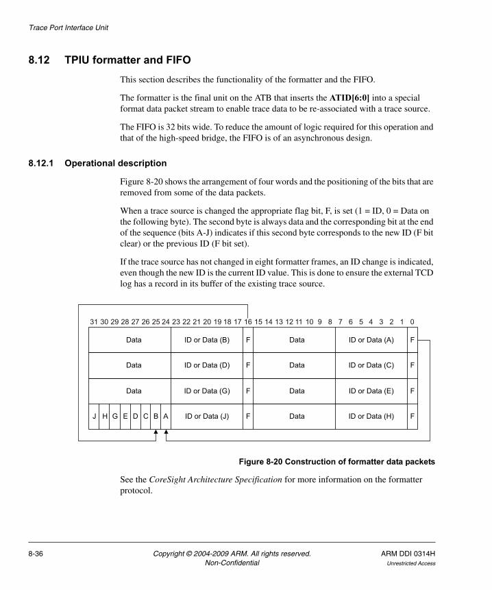
Trace Port Interface Unit
8.12 TPIU formatter and FIFOThis section describes the functionality of the formatter and the FIFO.
The formatter is the final unit on the ATB that inserts the ATID[6:0] into a special format data packet stream to enable trace data to be re-associated with a trace source.
The FIFO is 32 bits wide. To reduce the amount of logic required for this operation and that of the high-speed bridge, the FIFO is of an asynchronous design.
8.12.1 Operational description
Figure 8-20 shows the arrangement of four words and the positioning of the bits that are removed from some of the data packets.
When a trace source is changed the appropriate flag bit, F, is set (1 = ID, 0 = Data on the following byte). The second byte is always data and the corresponding bit at the end of the sequence (bits A-J) indicates if this second byte corresponds to the new ID (F bit clear) or the previous ID (F bit set).
If the trace source has not changed in eight formatter frames, an ID change is indicated, even though the new ID is the current ID value. This is done to ensure the external TCD log has a record in its buffer of the existing trace source.
Figure 8-20 Construction of formatter data packets
See the CoreSight Architecture Specification for more information on the formatter protocol.
ID or Data (J)
ID or Data (C)DataID or Data (D)Data
ID or Data (E)DataID or Data (G)Data
ID or Data (H)Data
FF
FF
FFJ ABCDEGH
31 30 29 28 27 26 25 24 23 22 21 20 19 18 17 16 15 14 13 12 11 10 9 8 7 6 5 4 3 2 1 0
ID or Data (B)Data ID or Data (A)Data FF
8-36 Copyright © 2004-2009 ARM. All rights reserved. ARM DDI 0314HNon-Confidential Unrestricted Access
Trace Port Interface Unit
8.12.2 Special trace source IDs
The following IDs are set aside for special purposes and must not be used under normal operation:
0x00 NULL trace source. Typically this is not used except when draining the formatter where filling of empty locations of frames is required.
0x70-0x7C Reserved.
0x7D Trigger event.
0x7E Reserved.
0x7F Reserved. This must never be used as a trace source ID because this can cause issues with correctly detecting synchronization packets.
8.12.3 Supported modes of operation
The formatter within the TPIU supports three basic modes of operation:-
Bypass IDs are not incorporated and raw trace data is emitted. It is assumed that the trace source is not changing. This requires the use of TRACECTL.
Normal Typical operation with capture devices that require use of a TRACECTL pin.
Continuous An extension of normal mode except when the control pin would normally indicate no data to be captured, there is data emitted that shows this fact. Also, triggers are embedded into the data stream because they cannot be indicated otherwise.
See the CoreSight Architecture Specification for more information on these modes.
8.12.4 Periodic synchronization
When the Formatter is in Continuous mode it can output more synchronization packets, both intraframe and interframe. When an interframe synchronization packet is emitted because of continuous mode, this causes the synchronization counter to restart counting. Full and half synchronization packets are output within interframe and intraframe respectively. See the CoreSight Architecture Specification for more information.
ARM DDI 0314H Copyright © 2004-2009 ARM. All rights reserved. 8-37Unrestricted Access Non-Confidential
Trace Port Interface Unit
8.13 Configuration optionsExisting TPAs that are only capable of operation with TRACECTL must only use the formatter in either bypass or normal mode, not continuous.
8.13.1 Configuration guidelines
TPIU configuration guidelines are as follows:
• It is recommended that following a trigger event within a multi-trace source configuration, a flush must be performed to ensure that all historical information that could relate to the trigger has been output.
• If Flush on Trigger Event and Stop on Trigger Event options are chosen then any data after the trigger is not captured by the TPA. When the TPIU is instructed to stop, it returns ATREADYS HIGH and does not store any of the accepted data.
• Although multiple flushes can be scheduled using Flush on Trigger Event, Flush on FLUSHIN and manual flush, when one of these requests have been made it masks any more requests of the same type, that is, repeated writing to the manual flush bit does not schedule multiple manual requests unless each is allowed to complete first. See Generation of flush on FLUSHIN on page 9-31, Generation of flush from a trigger event on page 9-32, and Generation of a flush on manual on page 9-33 for diagrams showing these sequences in detail.
• Unless multiple triggers are required, it is not advisable to set both Trigger on Trigger Event and Trigger on Flush Completion, if Flush on Trigger Event is also enabled. In addition, if Trigger on TRIGIN is enabled with this configuration, it can also cause multiple trigger markers from one trigger request.
8-38 Copyright © 2004-2009 ARM. All rights reserved. ARM DDI 0314HNon-Confidential Unrestricted Access
Trace Port Interface Unit
8.14 Example configuration scenariosThis section describes a number of configurations scenarios:
• Capturing trace after an event and stopping
• Only indicating triggers and still flushing on page 8-40
• Multiple trigger indications on page 8-40
• Independent triggering and flushing on page 8-41.
8.14.1 Capturing trace after an event and stopping
Two things must happen before trace capture can be stopped:
• a suitable length of time has to elapse to encompass knock-on effects within trace data
• all historical information relating to these previous events must have been emitted.
Figure 8-21 on page 8-40 shows a possible timeline of events where an event of interest, referred to as a trigger event, causes some trace that must be captured and thereafter the trace capture device can be stopped.
When one trace source is used, there is no requirement to flush the system, instead the length of the trigger counter delay can be increased to enable more trace to be generated, thereby pushing out historical information.
Traditionally only the initial trigger event is sent to the TPA at time t1, indicated using TRACECTL and a special encoding on TRACEDATA. This can still be done but if trace is stopped at this point, there might still be related trace stalled within the ATB system. Trigger signals are now abstracted from ATB through the CTI/CTM infrastructure. To allow all trace information to have been output that could have related to an internally generated trigger event, the system must be flushed after which trace capture can be safely stopped.
ARM DDI 0314H Copyright © 2004-2009 ARM. All rights reserved. 8-39Unrestricted Access Non-Confidential

Trace Port Interface Unit
Figure 8-21 Capturing trace after an event and stopping
In Figure 8-21 the action to cause trace capture to be stopped at time t3 could be:
• the TPA could watch for a trigger to be indicated through TRACECTL and stop
• the TPA could watch for a trigger to be indicated in the TRACEDATA stream that is, using continuous mode without the requirement for TRACECTL)
• the TPIU could automatically stop trace if the TPA only recognizes trace disable cycles, that is, it cannot act on trigger markers.
8.14.2 Only indicating triggers and still flushing
It is possible to still indicate a trigger at the soonest possible moment and cause a flush while at the same time still allowing externally requested flushes. This enables trace around a key event to be captured and all historical information to be stored within a period immediately following the trigger, and have some secondary event causing regular trace flushes.
8.14.3 Multiple trigger indications
After a trigger has been sent to external tools this could cause more than trace capture stopping. For example, in cases where the events immediately before the trigger might be important but only a small buffer is available, uploads to a host computer for decompression could occur so reducing the amount stored in the TPA. This would also be useful where the trigger originated from a device not directly associated with a trace source and is a marker for a repeating interesting event. See Figure 8-22 on page 8-41.
time
Internal event“Trigger”
Trace flush started
Trace flush completed
Trace capture stopped
t1 t2 t3
Trigger delay counter decreasing
Flush of ATB in progress (non-
determinable length)
8-40 Copyright © 2004-2009 ARM. All rights reserved. ARM DDI 0314HNon-Confidential Unrestricted Access
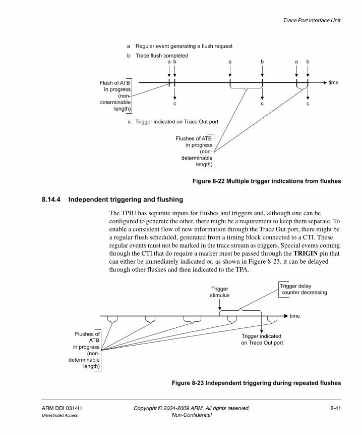
Trace Port Interface Unit
Figure 8-22 Multiple trigger indications from flushes
8.14.4 Independent triggering and flushing
The TPIU has separate inputs for flushes and triggers and, although one can be configured to generate the other, there might be a requirement to keep them separate. To enable a consistent flow of new information through the Trace Out port, there might be a regular flush scheduled, generated from a timing block connected to a CTI. These regular events must not be marked in the trace stream as triggers. Special events coming through the CTI that do require a marker must be passed through the TRIGIN pin that can either be immediately indicated or, as shown in Figure 8-23, it can be delayed through other flushes and then indicated to the TPA.
Figure 8-23 Independent triggering during repeated flushes
time
a a ab b b
c c c
Trigger indicated on Trace Out portc
Flush of ATB in progress
(non-determinable
length)
Regular event generating a flush requesta
Trace flush completedb
Flushes of ATB in progress
(non-determinable
length)
time
Trigger stimulus
Flushes of ATB
in progress (non-
determinable length)
Trigger indicated on Trace Out port
Trigger delay counter decreasing
ARM DDI 0314H Copyright © 2004-2009 ARM. All rights reserved. 8-41Unrestricted Access Non-Confidential

Trace Port Interface Unit
8-42 Copyright © 2004-2009 ARM. All rights reserved. ARM DDI 0314HNon-Confidential Unrestricted Access
Chapter 9 Embedded Trace Buffer
This chapter describes the Embedded Trace Buffer (ETB) for CoreSight. It contains the following sections:
• About the ETB for CoreSight on page 9-2
• ETB programmers model on page 9-5
• ETB register descriptions on page 9-8
• ETB CoreSight management registers on page 9-22
• ETB clocks, resets, and synchronization on page 9-24
• ETB Trace capture and formatting on page 9-25
• Flush assertion on page 9-30
• Triggers on page 9-34
• Write address generation for trace data storage on page 9-36
• Trace data storage on page 9-37
• APB configuration and RAM access on page 9-38
• Trace RAM on page 9-39
• Authentication requirements for CoreSight ETBs on page 9-40
• ETB RAM support on page 9-41
• ETB configuration options on page 9-42
• Comparisons with ETB11 on page 9-43.
ARM DDI 0314H Copyright © 2004-2009 ARM. All rights reserved. 9-1Unrestricted Access Non-Confidential
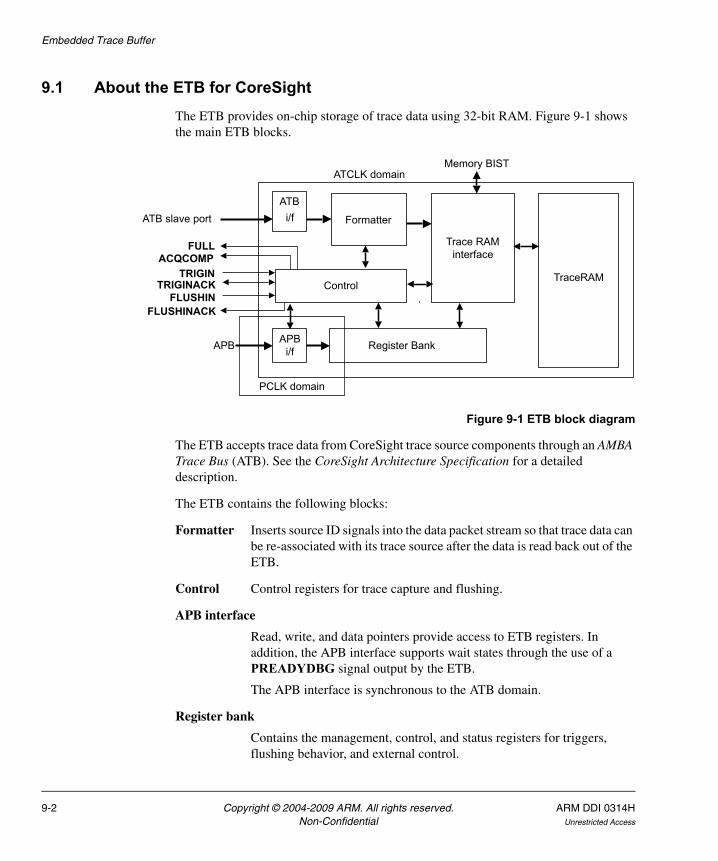
Embedded Trace Buffer
9.1 About the ETB for CoreSightThe ETB provides on-chip storage of trace data using 32-bit RAM. Figure 9-1 shows the main ETB blocks.
Figure 9-1 ETB block diagram
The ETB accepts trace data from CoreSight trace source components through an AMBA Trace Bus (ATB). See the CoreSight Architecture Specification for a detailed description.
The ETB contains the following blocks:
Formatter Inserts source ID signals into the data packet stream so that trace data can be re-associated with its trace source after the data is read back out of the ETB.
Control Control registers for trace capture and flushing.
APB interface
Read, write, and data pointers provide access to ETB registers. In addition, the APB interface supports wait states through the use of a PREADYDBG signal output by the ETB.
The APB interface is synchronous to the ATB domain.
Register bank
Contains the management, control, and status registers for triggers, flushing behavior, and external control.
PCLK domain
APBi/f Register Bank
Formatter
APB
ATCLK domain
ATB slave portATB
i/f
TraceRAMControl
Trace RAM interface
FULLACQCOMP
TRIGINTRIGINACK
FLUSHINFLUSHINACK
Memory BIST
9-2 Copyright © 2004-2009 ARM. All rights reserved. ARM DDI 0314HNon-Confidential Unrestricted Access
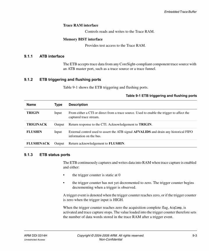
Embedded Trace Buffer
Trace RAM interface
Controls reads and writes to the Trace RAM.
Memory BIST interface
Provides test access to the Trace RAM.
9.1.1 ATB interface
The ETB accepts trace data from any CoreSight-compliant component trace source with an ATB master port, such as a trace source or a trace funnel.
9.1.2 ETB triggering and flushing ports
Table 9-1 shows the ETB triggering and flushing ports.
9.1.3 ETB status ports
The ETB continuously captures and writes data into RAM when trace capture is enabled and either:
• the trigger counter is static at 0
• the trigger counter has not yet decremented to zero. The trigger counter begins decrementing when a trigger is observed.
A trigger event is denoted when the trigger counter reaches zero, or if the trigger counter is zero when the trigger input is HIGH.
When the trigger counter reaches zero the acquisition complete flag, AcqComp, is activated and trace capture stops. The value loaded into the trigger counter therefore sets the number of data words stored in the trace RAM after a trigger event.
Table 9-1 ETB triggering and flushing ports
Name Type Description
TRIGIN Input From either a CTI or direct from a trace source. Used to enable the trigger to affect the captured trace stream.
TRIGINACK Output Return response to the CTI. Acknowledgement to TRIGIN.
FLUSHIN Input External control used to assert the ATB signal AFVALIDS and drain any historical FIFO information on the bus.
FLUSHINACK Output Return acknowledgement to FLUSHIN.
ARM DDI 0314H Copyright © 2004-2009 ARM. All rights reserved. 9-3Unrestricted Access Non-Confidential
Embedded Trace Buffer
Table 9-2 shows the ETB status ports.
9.1.4 Memory BIST interface
Table 9-3 shows the Memory BIST interface ports.
Table 9-2 ETB status ports
Name Type Description
ACQCOMP
Output When HIGH, indicates that trace acquisition is complete, that is, the trigger counter is at zero.
FULL Output When HIGH indicates that the ETB RAM has overflowed or wrapped around to address zero.
Table 9-3 ETB Memory BIST interface ports
Name Type Description
MBISTADDR [CSETB_ADDR_WIDTH-1:0] Input Address bus for the external BIST controller, active when MTESTON is HIGH.
CSETB_ADDR_WIDTH defines the address bus width used, and therefore the RAM depth supported.
MBISTCE Input Active HIGH chip select for external BIST controller, active when MTESTON is HIGH.
MBISTDIN[31:0] Input Write data bus for external BIST controller, active when MTESTON is HIGH.
MBISTDOUT[31:0] Output Read data bus for external BIST controller, active when MTESTON is HIGH.
MBISTWE Input Active HIGH write enable for external BIST controller, active when MTESTON is HIGH.
MTESTON Input Enable signal for the external BIST controller.
9-4 Copyright © 2004-2009 ARM. All rights reserved. ARM DDI 0314HNon-Confidential Unrestricted Access
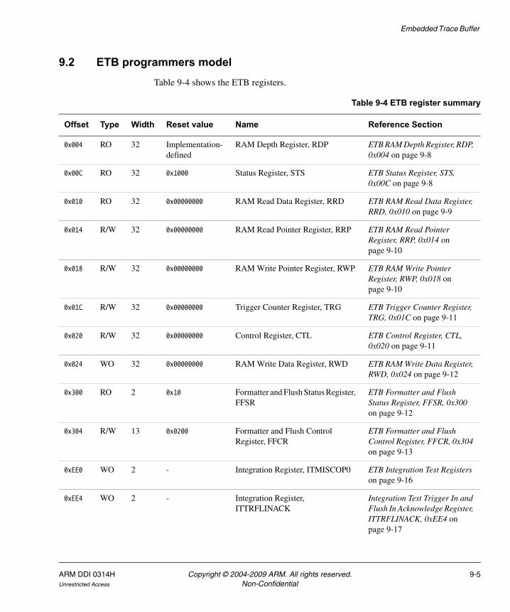
Embedded Trace Buffer
9.2 ETB programmers modelTable 9-4 shows the ETB registers.
Table 9-4 ETB register summary
Offset Type Width Reset value Name Reference Section
0x004 RO 32 Implementation- defined
RAM Depth Register, RDP ETB RAM Depth Register, RDP, 0x004 on page 9-8
0x00C RO 32 0x1000 Status Register, STS ETB Status Register, STS, 0x00C on page 9-8
0x010 RO 32 0x00000000 RAM Read Data Register, RRD ETB RAM Read Data Register, RRD, 0x010 on page 9-9
0x014 R/W 32 0x00000000 RAM Read Pointer Register, RRP ETB RAM Read Pointer Register, RRP, 0x014 on page 9-10
0x018 R/W 32 0x00000000 RAM Write Pointer Register, RWP ETB RAM Write Pointer Register, RWP, 0x018 on page 9-10
0x01C R/W 32 0x00000000 Trigger Counter Register, TRG ETB Trigger Counter Register, TRG, 0x01C on page 9-11
0x020 R/W 32 0x00000000 Control Register, CTL ETB Control Register, CTL, 0x020 on page 9-11
0x024 WO 32 0x00000000 RAM Write Data Register, RWD ETB RAM Write Data Register, RWD, 0x024 on page 9-12
0x300 RO 2 0x10 Formatter and Flush Status Register, FFSR
ETB Formatter and Flush Status Register, FFSR, 0x300 on page 9-12
0x304 R/W 13 0x0200 Formatter and Flush Control Register, FFCR
ETB Formatter and Flush Control Register, FFCR, 0x304 on page 9-13
0xEE0 WO 2 - Integration Register, ITMISCOP0 ETB Integration Test Registers on page 9-16
0xEE4 WO 2 - Integration Register, ITTRFLINACK
Integration Test Trigger In and Flush In Acknowledge Register, ITTRFLINACK, 0xEE4 on page 9-17
ARM DDI 0314H Copyright © 2004-2009 ARM. All rights reserved. 9-5Unrestricted Access Non-Confidential
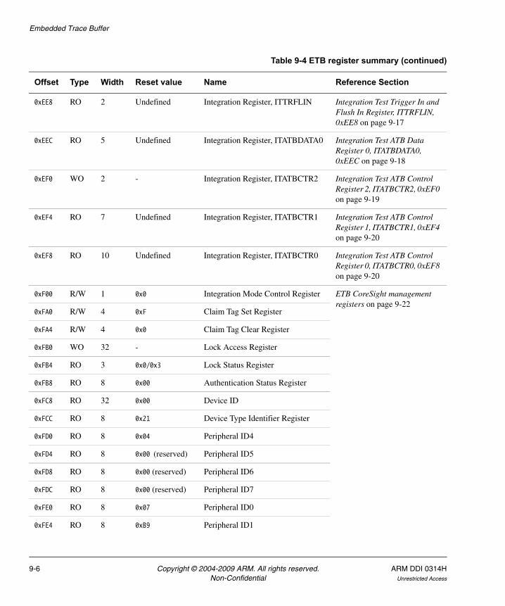
Embedded Trace Buffer
0xEE8 RO 2 Undefined Integration Register, ITTRFLIN Integration Test Trigger In and Flush In Register, ITTRFLIN, 0xEE8 on page 9-17
0xEEC RO 5 Undefined Integration Register, ITATBDATA0 Integration Test ATB Data Register 0, ITATBDATA0, 0xEEC on page 9-18
0xEF0 WO 2 - Integration Register, ITATBCTR2 Integration Test ATB Control Register 2, ITATBCTR2, 0xEF0 on page 9-19
0xEF4 RO 7 Undefined Integration Register, ITATBCTR1 Integration Test ATB Control Register 1, ITATBCTR1, 0xEF4 on page 9-20
0xEF8 RO 10 Undefined Integration Register, ITATBCTR0 Integration Test ATB Control Register 0, ITATBCTR0, 0xEF8 on page 9-20
0xF00 R/W 1 0x0 Integration Mode Control Register ETB CoreSight management registers on page 9-22
0xFA0 R/W 4 0xF Claim Tag Set Register
0xFA4 R/W 4 0x0 Claim Tag Clear Register
0xFB0 WO 32 - Lock Access Register
0xFB4 RO 3 0x0/0x3 Lock Status Register
0xFB8 RO 8 0x00 Authentication Status Register
0xFC8 RO 32 0x00 Device ID
0xFCC RO 8 0x21 Device Type Identifier Register
0xFD0 RO 8 0x04 Peripheral ID4
0xFD4 RO 8 0x00 (reserved) Peripheral ID5
0xFD8 RO 8 0x00 (reserved) Peripheral ID6
0xFDC RO 8 0x00 (reserved) Peripheral ID7
0xFE0 RO 8 0x07 Peripheral ID0
0xFE4 RO 8 0xB9 Peripheral ID1
Table 9-4 ETB register summary (continued)
Offset Type Width Reset value Name Reference Section
9-6 Copyright © 2004-2009 ARM. All rights reserved. ARM DDI 0314HNon-Confidential Unrestricted Access
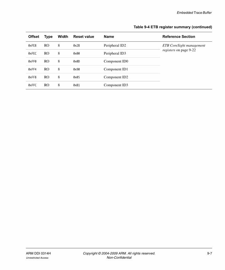
Embedded Trace Buffer
0xFE8 RO 8 0x2B Peripheral ID2 ETB CoreSight management registers on page 9-22
0xFEC RO 8 0x00 Peripheral ID3
0xFF0 RO 8 0x0D Component ID0
0xFF4 RO 8 0x90 Component ID1
0xFF8 RO 8 0x05 Component ID2
0xFFC RO 8 0xB1 Component ID3
Table 9-4 ETB register summary (continued)
Offset Type Width Reset value Name Reference Section
ARM DDI 0314H Copyright © 2004-2009 ARM. All rights reserved. 9-7Unrestricted Access Non-Confidential
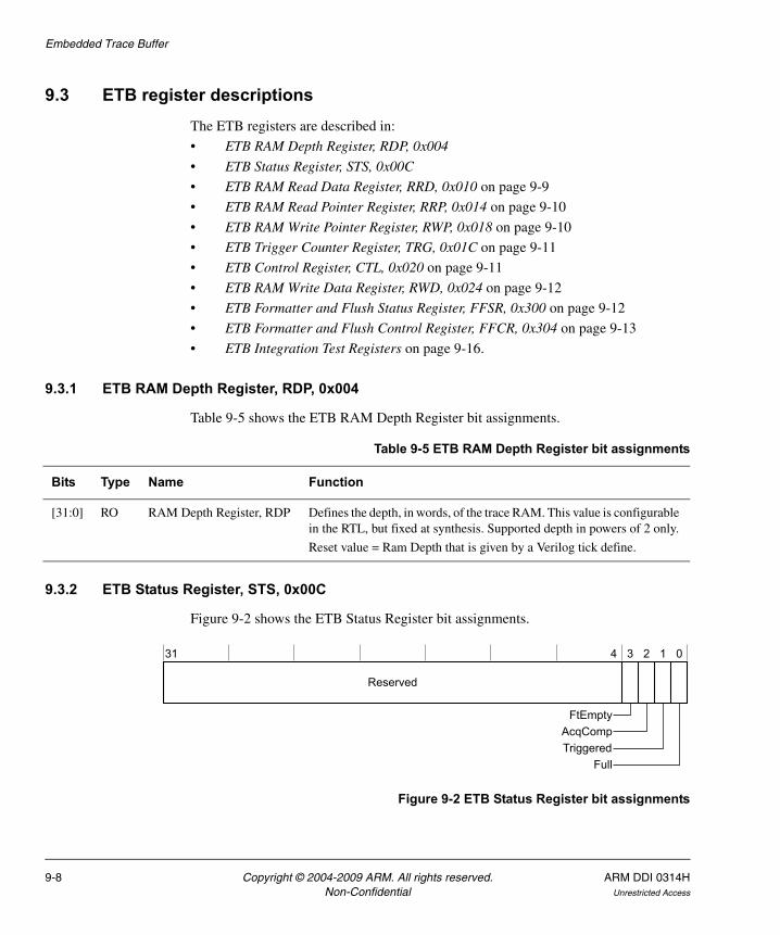
Embedded Trace Buffer
9.3 ETB register descriptionsThe ETB registers are described in:
• ETB RAM Depth Register, RDP, 0x004
• ETB Status Register, STS, 0x00C
• ETB RAM Read Data Register, RRD, 0x010 on page 9-9
• ETB RAM Read Pointer Register, RRP, 0x014 on page 9-10
• ETB RAM Write Pointer Register, RWP, 0x018 on page 9-10
• ETB Trigger Counter Register, TRG, 0x01C on page 9-11
• ETB Control Register, CTL, 0x020 on page 9-11
• ETB RAM Write Data Register, RWD, 0x024 on page 9-12
• ETB Formatter and Flush Status Register, FFSR, 0x300 on page 9-12
• ETB Formatter and Flush Control Register, FFCR, 0x304 on page 9-13
• ETB Integration Test Registers on page 9-16.
9.3.1 ETB RAM Depth Register, RDP, 0x004
Table 9-5 shows the ETB RAM Depth Register bit assignments.
9.3.2 ETB Status Register, STS, 0x00C
Figure 9-2 shows the ETB Status Register bit assignments.
Figure 9-2 ETB Status Register bit assignments
Table 9-5 ETB RAM Depth Register bit assignments
Bits Type Name Function
[31:0] RO RAM Depth Register, RDP Defines the depth, in words, of the trace RAM. This value is configurable in the RTL, but fixed at synthesis. Supported depth in powers of 2 only.
Reset value = Ram Depth that is given by a Verilog tick define.
Reserved
31 4 03
FtEmptyAcqCompTriggered
Full
2 1
9-8 Copyright © 2004-2009 ARM. All rights reserved. ARM DDI 0314HNon-Confidential Unrestricted Access
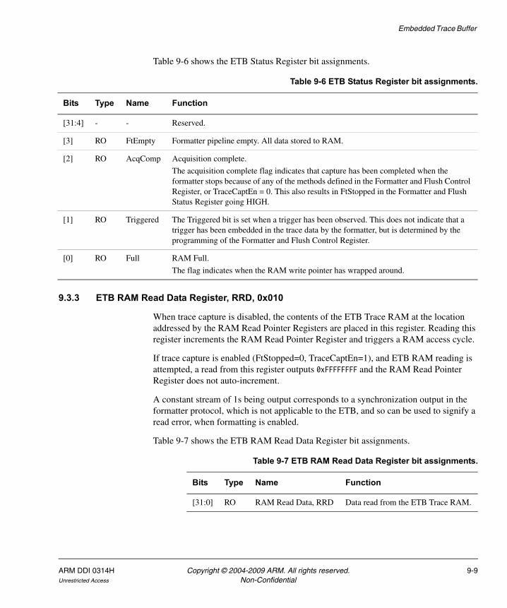
Embedded Trace Buffer
Table 9-6 shows the ETB Status Register bit assignments.
9.3.3 ETB RAM Read Data Register, RRD, 0x010
When trace capture is disabled, the contents of the ETB Trace RAM at the location addressed by the RAM Read Pointer Registers are placed in this register. Reading this register increments the RAM Read Pointer Register and triggers a RAM access cycle.
If trace capture is enabled (FtStopped=0, TraceCaptEn=1), and ETB RAM reading is attempted, a read from this register outputs 0xFFFFFFFF and the RAM Read Pointer Register does not auto-increment.
A constant stream of 1s being output corresponds to a synchronization output in the formatter protocol, which is not applicable to the ETB, and so can be used to signify a read error, when formatting is enabled.
Table 9-7 shows the ETB RAM Read Data Register bit assignments.
Table 9-6 ETB Status Register bit assignments.
Bits Type Name Function
[31:4] - - Reserved.
[3] RO FtEmpty Formatter pipeline empty. All data stored to RAM.
[2] RO AcqComp Acquisition complete.
The acquisition complete flag indicates that capture has been completed when the formatter stops because of any of the methods defined in the Formatter and Flush Control Register, or TraceCaptEn = 0. This also results in FtStopped in the Formatter and Flush Status Register going HIGH.
[1] RO Triggered The Triggered bit is set when a trigger has been observed. This does not indicate that a trigger has been embedded in the trace data by the formatter, but is determined by the programming of the Formatter and Flush Control Register.
[0] RO Full RAM Full.
The flag indicates when the RAM write pointer has wrapped around.
Table 9-7 ETB RAM Read Data Register bit assignments.
Bits Type Name Function
[31:0] RO RAM Read Data, RRD Data read from the ETB Trace RAM.
ARM DDI 0314H Copyright © 2004-2009 ARM. All rights reserved. 9-9Unrestricted Access Non-Confidential

Embedded Trace Buffer
9.3.4 ETB RAM Read Pointer Register, RRP, 0x014
The RAM Read Pointer Register sets the read pointer used to read entries from the Trace RAM over the APB interface. When this register is written to, a RAM access is initiated. The RAM Read Data Register is then updated. The register can also be read to determine the current memory location being referenced.
This register must not be written to when trace capture is enabled (FtStopped=0, TraceCaptEn=1). If access is attempted, the register is not updated.
Table 9-8 shows the ETB RAM Read Pointer Register bit assignments.
9.3.5 ETB RAM Write Pointer Register, RWP, 0x018
The RAM Write Pointer Register sets the write pointer used to write entries from the CoreSight bus into Trace RAM. During trace capture the pointer increments when the DataValid flag is asserted by the Formatter. When this register increments from its maximum value back to zero, the Full flag is set.
This register can also be written to over APB to set the pointer for write accesses carried out through the APB interface.
This register must not be written to when trace capture is enabled (FtStopped=0, TraceCaptEn=1). If access is attempted, the register is not updated. The register can also be read to determine the current memory location being referenced.
It is recommended that addresses are 128-bit aligned when the formatter is used in normal or continuous modes.
Table 9-9 shows the ETB RAM Write Pointer Register bit assignments.
Table 9-8 ETB RAM Read Pointer Register bit assignments.
Bits Type Name Function
[CSETB_ADDR_WIDTH-1:0] R/W RAM Read Pointer, RRP Sets the read pointer used to read entries from the Trace RAM over the APB interface.
Table 9-9 ETB RAM Write Pointer Register bit assignments.
Bits Type Name Function
[CSETB_ADDR_WIDTH-1:0] R/W RAM Write Pointer, RWP Sets the write pointer used to write entries from the CoreSight bus into the Trace RAM
9-10 Copyright © 2004-2009 ARM. All rights reserved. ARM DDI 0314HNon-Confidential Unrestricted Access

Embedded Trace Buffer
9.3.6 ETB Trigger Counter Register, TRG, 0x01C
The Trigger Counter Register disables write access to the Trace RAM by stopping the Formatter after a defined number of words have been stored following the trigger event. The number of 32-bit words written into the Trace RAM following the trigger event is equal to the value stored in this register+1.
Table 9-10 shows the ETB Trigger Counter Register bit assignments.
9.3.7 ETB Control Register, CTL, 0x020
Figure 9-3 shows the ETB Control Register bit assignments.
Figure 9-3 ETB Control Register bit assignments
Table 9-10 ETB Trigger Counter Register bit assignments.
Bits Type Name Function
[31:CSETB_ADDR_WIDTH] - - Reserved.
CSETB_ADDR_WIDTH defines the address bus width, and the RAM depth supported
[CSETB_ADDR_WIDTH-1:0] R/W Trigger Counter, TRG Trigger Counter Register.
The counter is used as follows:
• Trace after
The counter is set to a large value, slightly less than the number of entries in the RAM.
• Trace before
The counter is set to a small value.
• Trace about
The counter is set to half the depth of the Trace RAM.
This register must not be written to when trace capture is enabled (FtStopped=0, TraceCaptEn=1). If a write is attempted, the register is not updated. A read access is permitted with trace capture enabled.
Reserved
31 0
TraceCaptEn
1
ARM DDI 0314H Copyright © 2004-2009 ARM. All rights reserved. 9-11Unrestricted Access Non-Confidential

Embedded Trace Buffer
Table 9-11 shows the ETB Control Register bit assignments.
9.3.8 ETB RAM Write Data Register, RWD, 0x024
Table 9-12 shows the ETB RAM Write Data Register bit assignments.
9.3.9 ETB Formatter and Flush Status Register, FFSR, 0x300
This register indicates the implemented Trigger Counter multipliers and other supported features of the trigger system.
Figure 9-4 on page 9-13 shows the ETB Formatter and Flush Status Register bit assignments.
Table 9-11 ETB Control Register bit assignments.
Bits Type Name Function
[31:1] - - Reserved
[0] R/W TraceCaptEn ETB Trace Capture Enable.
1 = enable trace capture
0 = disable trace capture.
This is the master enable bit forcing FtStopped HIGH when TraceCaptEn is LOW. When capture is disabled, any remaining data in the ATB formatter is stored to RAM. When all data is stored the formatter outputs FtStopped. Capture is fully disabled, or complete, when FtStopped goes HIGH. See ETB Formatter and Flush Status Register, FFSR, 0x300.
Table 9-12 ETB RAM Write Data Register bit assignments
Bits Type Name Function
[31:0] R/W RAM Write Data Register, RWD Data written to the ETB Trace RAM.
When trace capture is disabled, the contents of this register are placed into the ETB Trace RAM when this register is written to. Writing to this register increments the RAM Write Pointer Register.
If trace capture is enabled, and this register is accessed, then a read from this register outputs 0xFFFFFFFF. Reads of this register never increment the RAM Write Pointer Register. A constant stream of 1s being output corresponds to a synchronization output from the ETB. If a write access is attempted, the data is not written into Trace RAM.
9-12 Copyright © 2004-2009 ARM. All rights reserved. ARM DDI 0314HNon-Confidential Unrestricted Access

Embedded Trace Buffer
Figure 9-4 ETB Formatter and Flush Status Register bit assignments
Table 9-13 shows the ETB Formatter and Flush Status Register bit assignments.
9.3.10 ETB Formatter and Flush Control Register, FFCR, 0x304
This register indicates the stop, trigger, and flush events. Figure 9-5 on page 9-14 shows the ETB Formatter and Flush Control Register bit assignments.
Reserved
31 2 1 0
FtStoppedFlInProg
Table 9-13 ETB Formatter and Flush Status Register bit assignments
Bits Type Name Description
[31:2] - - Reserved RAZ/SBZP.
[1] RO FtStopped Formatter stopped. The formatter has received a stop request signal and all trace data and post-amble has been output. Any more trace data on the ATB interface is ignored and ATREADYS goes HIGH.
[0] RO FlInProg Flush In Progress. This is an indication of the current state of AFVALIDS.
ARM DDI 0314H Copyright © 2004-2009 ARM. All rights reserved. 9-13Unrestricted Access Non-Confidential
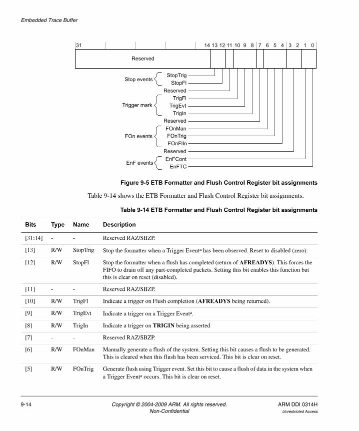
Embedded Trace Buffer
Figure 9-5 ETB Formatter and Flush Control Register bit assignments
Table 9-14 shows the ETB Formatter and Flush Control Register bit assignments.
Reserved
31 14 13 12 11 10 9 8 7 6 5 4 3 2 1 0
Reserved
Reserved
TrigFlTrigEvt
TrigIn
FOnManFOnTrigFOnFlIn
StopTrigStopFl
ReservedEnFCont
EnFTC
Stop events
Trigger mark
FOn events
EnF events
Table 9-14 ETB Formatter and Flush Control Register bit assignments
Bits Type Name Description
[31:14] - - Reserved RAZ/SBZP.
[13] R/W StopTrig Stop the formatter when a Trigger Eventa has been observed. Reset to disabled (zero).
[12] R/W StopFl Stop the formatter when a flush has completed (return of AFREADYS). This forces the FIFO to drain off any part-completed packets. Setting this bit enables this function but this is clear on reset (disabled).
[11] - - Reserved RAZ/SBZP.
[10] R/W TrigFl Indicate a trigger on Flush completion (AFREADYS being returned).
[9] R/W TrigEvt Indicate a trigger on a Trigger Eventa.
[8] R/W TrigIn Indicate a trigger on TRIGIN being asserted
[7] - - Reserved RAZ/SBZP.
[6] R/W FOnMan Manually generate a flush of the system. Setting this bit causes a flush to be generated. This is cleared when this flush has been serviced. This bit is clear on reset.
[5] R/W FOnTrig Generate flush using Trigger event. Set this bit to cause a flush of data in the system when a Trigger Eventa occurs. This bit is clear on reset.
9-14 Copyright © 2004-2009 ARM. All rights reserved. ARM DDI 0314HNon-Confidential Unrestricted Access

Embedded Trace Buffer
To disable formatting and put the formatter into bypass mode, bits 1 and 0 must be clear. If both bits are set, then the formatter inserts triggers into the formatted stream.All three flush generating conditions can be enabled together. However, if a second or third flush event is generated then the current flush completes before the next flush is serviced. Flush from FLUSHIN takes priority over flush from Trigger, which in turn completes before a manually activated flush.All trigger indication conditions can be enabled simultaneously although this can cause the appearance of multiple triggers if flush using trigger is also enabled.
Both 'Stop On' settings can be enabled although if flush on trigger, FOnTrig, is set then none of the flushed data is stored. When the system stops, it returns ATREADY and does not store the accepted data packets. This is to stop stalling of any other connected devices using a Trace Replicator.
If an event in the Formatter and Flush Control Register is required, it must be enabled before the originating event starts. Because requests from flushes and triggers can originate in an asynchronous clock domain, the exact time the component acts on the request cannot be determined with respect to configuring the control.
Note To perform a stop on flush completion through a manually-generated flush request, two write operations to the register are required:
• one to enable the stop event, if it is not already enabled
• one to generate the manual flush.
[4] R/W FOnFlIn Generate flush using the FLUSHIN interface. Set this bit to enable use of the FLUSHIN connection. This bit is clear on reset.
[3:2] - - Reserved RAZ/SBZP.
[1] R/W EnFCont Continuous Formatting. Continuous mode in the ETB corresponds to normal mode with the embedding of triggers. Can only be changed when FtStopped is HIGH. This bit is clear on reset.
[0] R/W EnFTC Enable Formatting. Do not embed Triggers into the formatted stream. Trace disable cycles and triggers are indicated by TRACECTL, where fitted. Can only be changed when FtStopped is HIGH. This bit is clear on reset.
a. A Trigger Event is defined as when the Trigger counter reaches zero (where fitted) or, in the case of the trigger counter being zero (or not fitted), when TRIGIN is HIGH.
Table 9-14 ETB Formatter and Flush Control Register bit assignments (continued)
Bits Type Name Description
ARM DDI 0314H Copyright © 2004-2009 ARM. All rights reserved. 9-15Unrestricted Access Non-Confidential
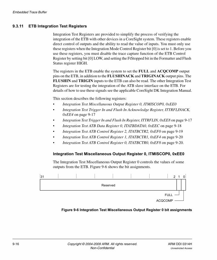
Embedded Trace Buffer
9.3.11 ETB Integration Test Registers
Integration Test Registers are provided to simplify the process of verifying the integration of the ETB with other devices in a CoreSight system. These registers enable direct control of outputs and the ability to read the value of inputs. You must only use these registers when the Integration Mode Control Register bit [0] is set to 1. Before you use these registers, you must disable the trace capture function of the ETB Control Register by setting bit [0] LOW, and setting the FtStopped bit in the Formatter and Flush Status register HIGH.
The registers in the ETB enable the system to set the FULL and ACQCOMP output pins on the ETB, in addition to the FLUSHINACK and TRIGINACK output pins. The FLUSHIN and TRIGIN inputs to the ETB can also be read. The other Integration Test Registers are for testing the integration of the ATB slave interface on the ETB. For details of how to use these signals see the applicable CoreSight DK Integration Manual.
This section describes the following registers:
• Integration Test Miscellaneous Output Register 0, ITMISCOP0, 0xEE0
• Integration Test Trigger In and Flush In Acknowledge Register, ITTRFLINACK, 0xEE4 on page 9-17
• Integration Test Trigger In and Flush In Register, ITTRFLIN, 0xEE8 on page 9-17
• Integration Test ATB Data Register 0, ITATBDATA0, 0xEEC on page 9-18
• Integration Test ATB Control Register 2, ITATBCTR2, 0xEF0 on page 9-19
• Integration Test ATB Control Register 1, ITATBCTR1, 0xEF4 on page 9-20
• Integration Test ATB Control Register 0, ITATBCTR0, 0xEF8 on page 9-20.
Integration Test Miscellaneous Output Register 0, ITMISCOP0, 0xEE0
The Integration Test Miscellaneous Output Register 0 controls the values of some outputs from the ETB. Figure 9-6 shows the bit assignments.
Figure 9-6 Integration Test Miscellaneous Output Register 0 bit assignments
31 2 1 0
FULL
ACQCOMP
Reserved
9-16 Copyright © 2004-2009 ARM. All rights reserved. ARM DDI 0314HNon-Confidential Unrestricted Access
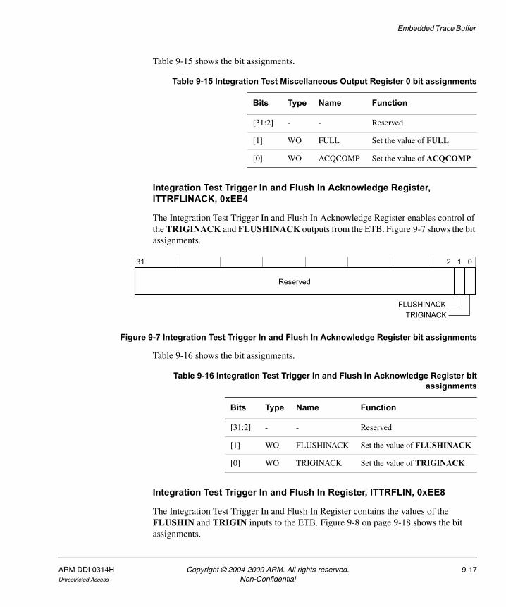
Embedded Trace Buffer
Table 9-15 shows the bit assignments.
Integration Test Trigger In and Flush In Acknowledge Register, ITTRFLINACK, 0xEE4
The Integration Test Trigger In and Flush In Acknowledge Register enables control of the TRIGINACK and FLUSHINACK outputs from the ETB. Figure 9-7 shows the bit assignments.
Figure 9-7 Integration Test Trigger In and Flush In Acknowledge Register bit assignments
Table 9-16 shows the bit assignments.
Integration Test Trigger In and Flush In Register, ITTRFLIN, 0xEE8
The Integration Test Trigger In and Flush In Register contains the values of the FLUSHIN and TRIGIN inputs to the ETB. Figure 9-8 on page 9-18 shows the bit assignments.
Table 9-15 Integration Test Miscellaneous Output Register 0 bit assignments
Bits Type Name Function
[31:2] - - Reserved
[1] WO FULL Set the value of FULL
[0] WO ACQCOMP Set the value of ACQCOMP
31 2 1 0
FLUSHINACKTRIGINACK
Reserved
Table 9-16 Integration Test Trigger In and Flush In Acknowledge Register bitassignments
Bits Type Name Function
[31:2] - - Reserved
[1] WO FLUSHINACK Set the value of FLUSHINACK
[0] WO TRIGINACK Set the value of TRIGINACK
ARM DDI 0314H Copyright © 2004-2009 ARM. All rights reserved. 9-17Unrestricted Access Non-Confidential
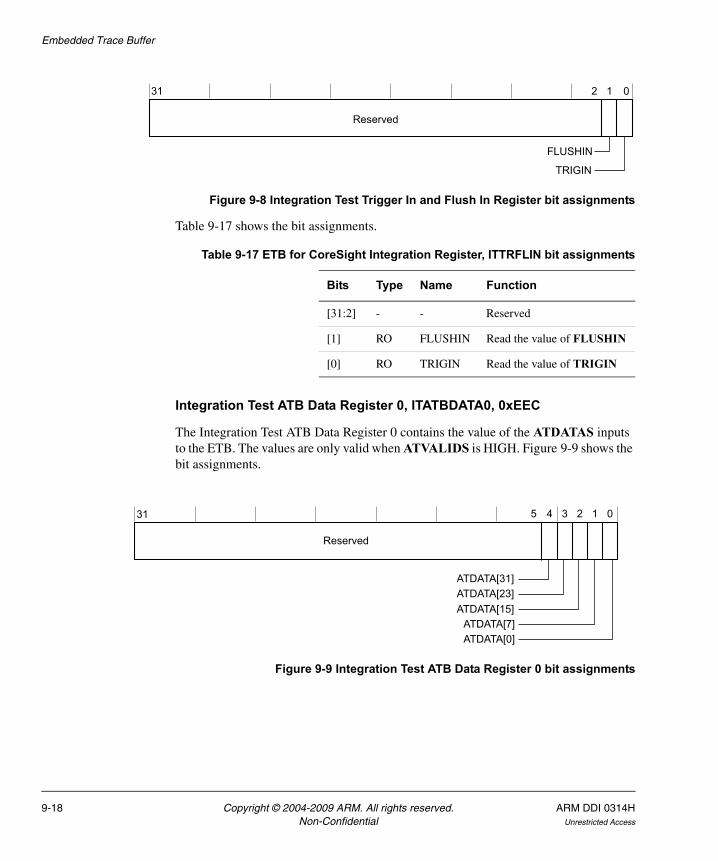
Embedded Trace Buffer
Figure 9-8 Integration Test Trigger In and Flush In Register bit assignments
Table 9-17 shows the bit assignments.
Integration Test ATB Data Register 0, ITATBDATA0, 0xEEC
The Integration Test ATB Data Register 0 contains the value of the ATDATAS inputs to the ETB. The values are only valid when ATVALIDS is HIGH. Figure 9-9 shows the bit assignments.
Figure 9-9 Integration Test ATB Data Register 0 bit assignments
31 2 1 0
FLUSHIN
TRIGIN
Reserved
Table 9-17 ETB for CoreSight Integration Register, ITTRFLIN bit assignments
Bits Type Name Function
[31:2] - - Reserved
[1] RO FLUSHIN Read the value of FLUSHIN
[0] RO TRIGIN Read the value of TRIGIN
31 4 3 2 1
Reserved
0
ATDATA[31]ATDATA[23]ATDATA[15]
ATDATA[0]ATDATA[7]
5
9-18 Copyright © 2004-2009 ARM. All rights reserved. ARM DDI 0314HNon-Confidential Unrestricted Access
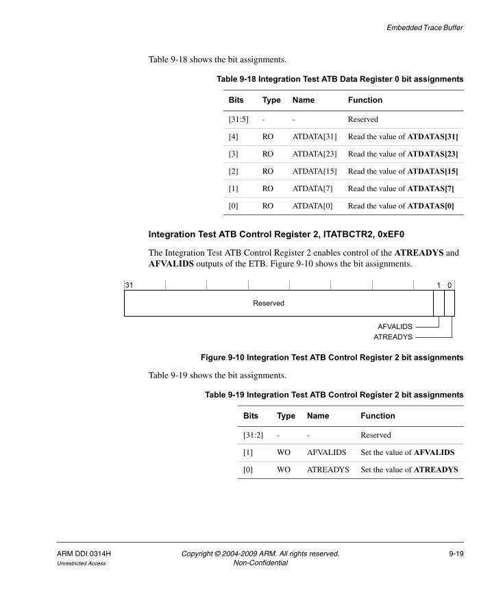
Embedded Trace Buffer
Table 9-18 shows the bit assignments.
Integration Test ATB Control Register 2, ITATBCTR2, 0xEF0
The Integration Test ATB Control Register 2 enables control of the ATREADYS and AFVALIDS outputs of the ETB. Figure 9-10 shows the bit assignments.
Figure 9-10 Integration Test ATB Control Register 2 bit assignments
Table 9-19 shows the bit assignments.
Table 9-18 Integration Test ATB Data Register 0 bit assignments
Bits Type Name Function
[31:5] - - Reserved
[4] RO ATDATA[31] Read the value of ATDATAS[31]
[3] RO ATDATA[23] Read the value of ATDATAS[23]
[2] RO ATDATA[15] Read the value of ATDATAS[15]
[1] RO ATDATA[7] Read the value of ATDATAS[7]
[0] RO ATDATA[0] Read the value of ATDATAS[0]
31
Reserved
01
AFVALIDSATREADYS
Table 9-19 Integration Test ATB Control Register 2 bit assignments
Bits Type Name Function
[31:2] - - Reserved
[1] WO AFVALIDS Set the value of AFVALIDS
[0] WO ATREADYS Set the value of ATREADYS
ARM DDI 0314H Copyright © 2004-2009 ARM. All rights reserved. 9-19Unrestricted Access Non-Confidential
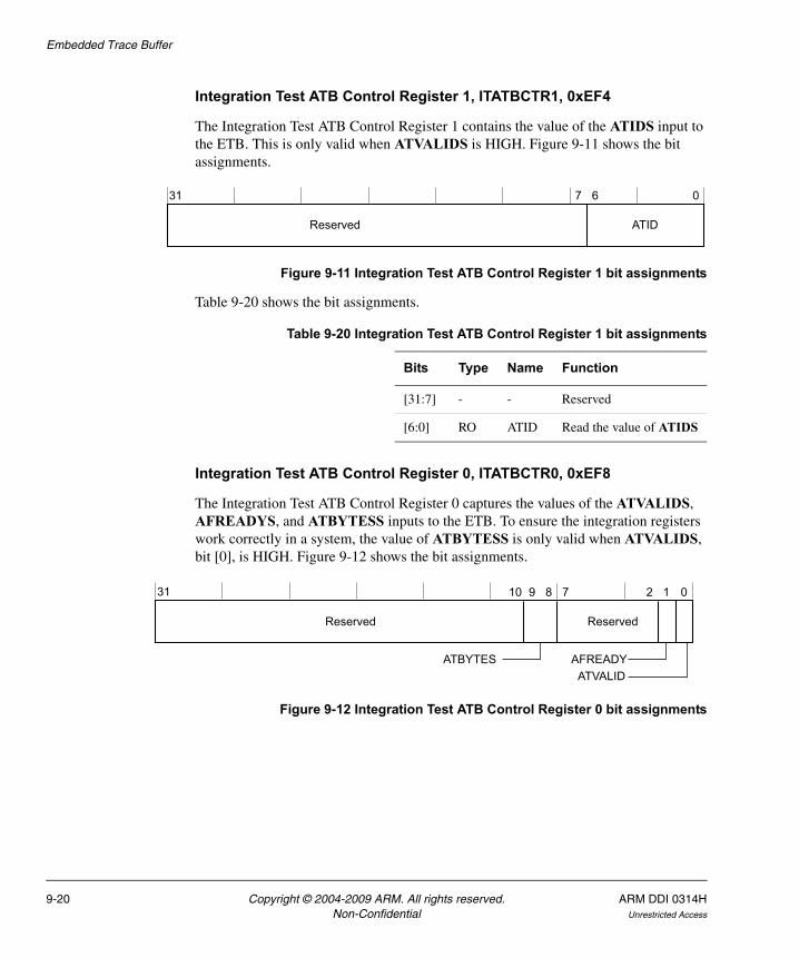
Embedded Trace Buffer
Integration Test ATB Control Register 1, ITATBCTR1, 0xEF4
The Integration Test ATB Control Register 1 contains the value of the ATIDS input to the ETB. This is only valid when ATVALIDS is HIGH. Figure 9-11 shows the bit assignments.
Figure 9-11 Integration Test ATB Control Register 1 bit assignments
Table 9-20 shows the bit assignments.
Integration Test ATB Control Register 0, ITATBCTR0, 0xEF8
The Integration Test ATB Control Register 0 captures the values of the ATVALIDS, AFREADYS, and ATBYTESS inputs to the ETB. To ensure the integration registers work correctly in a system, the value of ATBYTESS is only valid when ATVALIDS, bit [0], is HIGH. Figure 9-12 shows the bit assignments.
Figure 9-12 Integration Test ATB Control Register 0 bit assignments
31
Reserved
6 0
ATID
7
Table 9-20 Integration Test ATB Control Register 1 bit assignments
Bits Type Name Function
[31:7] - - Reserved
[6:0] RO ATID Read the value of ATIDS
31
Reserved
01
AFREADYATVALID
9 8
Reserved
ATBYTES
10 7 2
9-20 Copyright © 2004-2009 ARM. All rights reserved. ARM DDI 0314HNon-Confidential Unrestricted Access
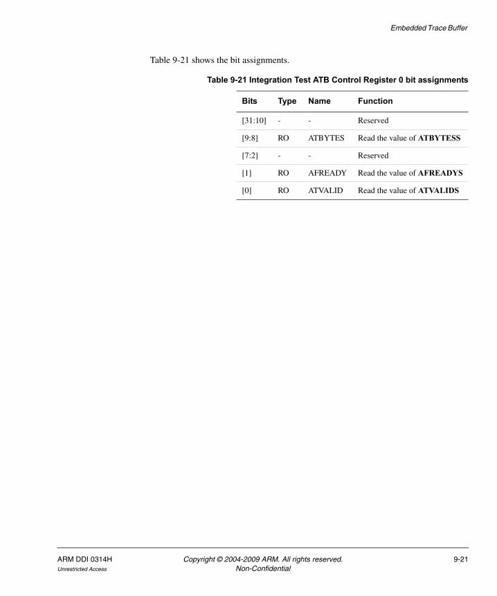
Embedded Trace Buffer
Table 9-21 shows the bit assignments.
Table 9-21 Integration Test ATB Control Register 0 bit assignments
Bits Type Name Function
[31:10] - - Reserved
[9:8] RO ATBYTES Read the value of ATBYTESS
[7:2] - - Reserved
[1] RO AFREADY Read the value of AFREADYS
[0] RO ATVALID Read the value of ATVALIDS
ARM DDI 0314H Copyright © 2004-2009 ARM. All rights reserved. 9-21Unrestricted Access Non-Confidential
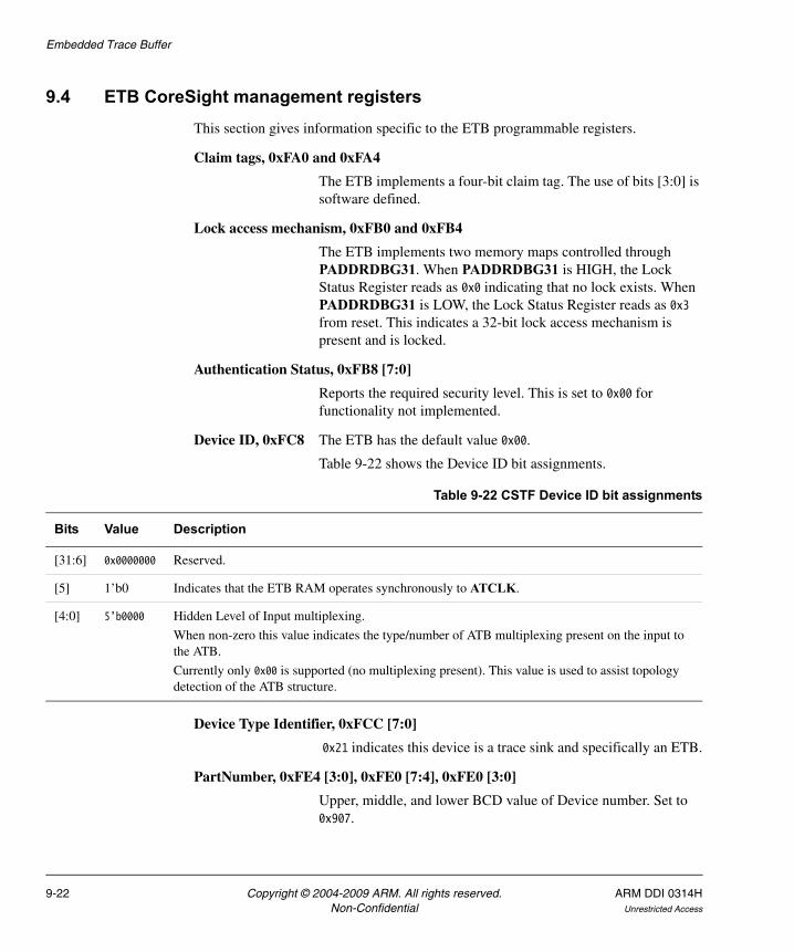
Embedded Trace Buffer
9.4 ETB CoreSight management registersThis section gives information specific to the ETB programmable registers.
Claim tags, 0xFA0 and 0xFA4
The ETB implements a four-bit claim tag. The use of bits [3:0] is software defined.
Lock access mechanism, 0xFB0 and 0xFB4
The ETB implements two memory maps controlled through PADDRDBG31. When PADDRDBG31 is HIGH, the Lock Status Register reads as 0x0 indicating that no lock exists. When PADDRDBG31 is LOW, the Lock Status Register reads as 0x3 from reset. This indicates a 32-bit lock access mechanism is present and is locked.
Authentication Status, 0xFB8 [7:0]
Reports the required security level. This is set to 0x00 for functionality not implemented.
Device ID, 0xFC8 The ETB has the default value 0x00.
Table 9-22 shows the Device ID bit assignments.
Device Type Identifier, 0xFCC [7:0]
0x21 indicates this device is a trace sink and specifically an ETB.
PartNumber, 0xFE4 [3:0], 0xFE0 [7:4], 0xFE0 [3:0]
Upper, middle, and lower BCD value of Device number. Set to 0x907.
Table 9-22 CSTF Device ID bit assignments
Bits Value Description
[31:6] 0x0000000 Reserved.
[5] 1’b0 Indicates that the ETB RAM operates synchronously to ATCLK.
[4:0] 5’b0000 Hidden Level of Input multiplexing.
When non-zero this value indicates the type/number of ATB multiplexing present on the input to the ATB.
Currently only 0x00 is supported (no multiplexing present). This value is used to assist topology detection of the ATB structure.
9-22 Copyright © 2004-2009 ARM. All rights reserved. ARM DDI 0314HNon-Confidential Unrestricted Access
Embedded Trace Buffer
Designer JEP106 value, 0xFD0[3:0], 0xFE8[2:0], 0xFE4[7:4]
The ETB is identified as an ARM component with a JEP106 identity at 0x3B and a JEP106 continuation code at 0x4 (fifth bank).
Component class, 0xFF4[7:4]
The ETB complies to the CoreSight class of components and this value is set to 0x9.
See Table 1-1 on page 1-4 for the current value of the revision field at offset 0xFE8[7:4].
ARM DDI 0314H Copyright © 2004-2009 ARM. All rights reserved. 9-23Unrestricted Access Non-Confidential
Embedded Trace Buffer
9.5 ETB clocks, resets, and synchronizationThis section describes ETB clocks, resets, and synchronization.
9.5.1 ETB clock domains
The ETB has two clock domains:
PCLKDBG Drives the APB interface and selected control registers.
ATCLK Drives the ATB interface, all control logic, and RAM.
9.5.2 ETB resets
ATRESETn resets all of the ETB registers in the ATCLK domain. ATRESETn must be synchronized externally in the CoreSight infrastructure by a global CoreSight reset signal that asserts ATRESETn asynchronously and deasserts ATRESETn synchronously with ATCLK.
PRESETDBGn resets the APB interface of the ETB. PRESETDBGn must be synchronized externally in the CoreSight infrastructure by a global CoreSight reset signal that asserts PRESETDBGn asynchronously and deasserts PRESETDBGn synchronously with PCLKDBG.
9.5.3 ETB synchronization
ATCLK and PCLKDBG are synchronous domains.
Note PCLKDBG must be equivalent to, or an integer division of ATCLK.
9-24 Copyright © 2004-2009 ARM. All rights reserved. ARM DDI 0314HNon-Confidential Unrestricted Access
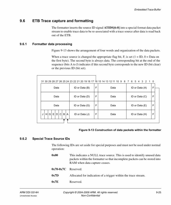
Embedded Trace Buffer
9.6 ETB Trace capture and formattingThe formatter inserts the source ID signal ATIDS[6:0] into a special format data packet stream to enable trace data to be re-associated with a trace source after data is read back out of the ETB.
9.6.1 Formatter data processing
Figure 9-13 shows the arrangement of four words and organization of the data packets.
When a trace source is changed the appropriate flag bit, F, is set (1 = ID, 0 = Data on the first byte). The second byte is always data. The corresponding bit at the end of the sequence (bits A to J) indicates if this second byte corresponds to the new ID (bit clear) or the previous ID (bit set).
Figure 9-13 Construction of data packets within the formatter
9.6.2 Special Trace Source IDs
The following IDs are set aside for special purposes and must not be used under normal operation:
0x00 This indicates a NULL trace source. This is used to identify unused data packets within the formatter so that incomplete packets can be stored into RAM when data capture ceases.
0x70-0x7C Reserved.
0x7D Allocated for indication of a trigger within the trace stream.
0x7E Reserved.
ID or Data (J)
ID or Data (C)DataID or Data (D)Data
ID or Data (E)DataID or Data (G)Data
ID or Data (H)Data
FF
FF
FFJ ABCDEGH
31 30 29 28 27 26 25 24 23 22 21 20 19 18 17 16 15 14 13 12 11 10 9 8 7 6 5 4 3 2 1 0
ID or Data (B)Data ID or Data (A)Data FF
ARM DDI 0314H Copyright © 2004-2009 ARM. All rights reserved. 9-25Unrestricted Access Non-Confidential
Embedded Trace Buffer
0x7F Reserved. This ID must never be used as a trace source ID because it can cause issues with correctly detecting the synchronization packet.
9.6.3 Special modes of operation
The Formatter supports two distinct modes of operation as specified by bits [1:0] in the Formatter and Flush Control Register:
Bypass In this mode, no formatting information is inserted into the trace stream and a raw reproduction of the incoming trace stream is stored. If any bytes remain in the formatter when tracing is stopped, because of non 32-bit ATDATAS, then the word stored to RAM is appended with a single logic 1 bit and filled in with zeros. A second word, 0x00000000 is then stored. If no bytes remain in the formatter, when capture is stopped, four additional words are stored, 0x00000001 then three words of 0x00000000.
When data is later decompressed it is then possible to determine that a post-amble is present by back tracking the trailing zero data at then end of the trace stream until the last single bit at logic 1 is detected. All data preceding this first logic 1 is then treated as decompressible data. When all data has been stored in the RAM, FtStopped in the Formatter and Flush Status Register is set HIGH.
Note This mode assumes that the source ID is not changing.
Normal Normal mode has the option of embedding triggers into the data packets.
Formatting information is added to indicate the change of source ID along with the associated wrapping additions, as described in TPIU formatter and FIFO on page 8-36. If any data remains in the formatter when tracing is stopped then the formatter is filled with NULL packets (ID = 0x00) to ensure all data is stored in RAM. When all remaining data has been stored in the RAM, FtStopped in the Formatter and Flush Status Register is set HIGH.
Continuous Continuous mode in the ETB corresponds to normal mode with the embedding of triggers. Unlike continuous mode in the TPIU, no formatter synchronization packets are added because alignment of data to the RAM locations is assumed.
9-26 Copyright © 2004-2009 ARM. All rights reserved. ARM DDI 0314HNon-Confidential Unrestricted Access
Embedded Trace Buffer
9.6.4 Stopping tracing
The stopping of tracing is indicated by FtStopped HIGH in the Formatter and Flush Status Register. This is set by:
• TraceCaptEn = 0 in the Control Register.
• A trigger event occurring, TRIGIN goes HIGH and the Trigger Counter Register reaches zero, and StopTrig set HIGH in the Formatter and Flush Control Register (0x304).
• A flush completing and StopFl set HIGH in the Formatter and Flush Control Register.
Figure 9-14 on page 9-28 shows a flowchart defining the conditions for stopping trace capture.
ARM DDI 0314H Copyright © 2004-2009 ARM. All rights reserved. 9-27Unrestricted Access Non-Confidential
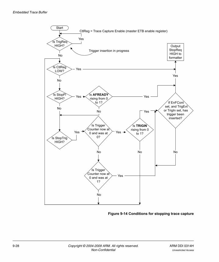
Embedded Trace Buffer
Figure 9-14 Conditions for stopping trace capture
Is CtlRegLOW?
CtlReg = Trace Capture Enable (master ETB enable register)
Is StopFl HIGH?
Is StopTrig HIGH?
Is AFREADY rising from 0
to 1?
Is TRIGIN rising from 0
to 1?
Yes
No
Yes
NoNo
Yes
Yes
No
Yes
Start
Is TrigReq HIGH?
No
Yes
Trigger insertion in progress
Is Trigger Counter now at
0 and was at 0?
Is Trigger Counter now at
0 and was at 1?
No
No No
If EnFCont set, and TrigEvt or TrigIn set, has
trigger been inserted?
Output StopReq HIGH to formatter
Yes
Yes
Yes
9-28 Copyright © 2004-2009 ARM. All rights reserved. ARM DDI 0314HNon-Confidential Unrestricted Access

Embedded Trace Buffer
StopTrig and StopFl in the Formatter and Flush Control Register can be enabled at the same time. For example, if FOnTrig in the Formatter and Flush Control Register is set to perform a flush on a trigger event, but StopTrig is HIGH, none of the flushed data is stored, because StopTrig is HIGH. If the situation requires that all the flushed data is captured StopTrig must be LOW and StopFl must be HIGH in this situation.
When the formatter stops, ATREADYS is output HIGH to prevent an ATB bus from stalling, which is important when a replicator is present, but the received data is ignored.
ARM DDI 0314H Copyright © 2004-2009 ARM. All rights reserved. 9-29Unrestricted Access Non-Confidential
Embedded Trace Buffer
9.7 Flush assertionAll three flush generating conditions can be enabled together:
• flush from FLUSHIN• flush from Trigger
• manually activated flush.
If more flush events are generated while a flush is in progress, the current flush is serviced before the next flush is started. Only one request for each source of flush can be pended. If a subsequent flush request signal is deasserted while the flush is still being serviced or pended, a second flush is not generated.
Flush from FLUSHIN takes priority over Flush from Trigger, which in turn is completed before a manually activated flush. The operation of the flush mechanism is defined in the CoreSight Architecture Specification.
Figure 9-15 on page 9-31 shows a flowchart defining the conditions for generating a flush on the ATB interface.
9-30 Copyright © 2004-2009 ARM. All rights reserved. ARM DDI 0314HNon-Confidential Unrestricted Access
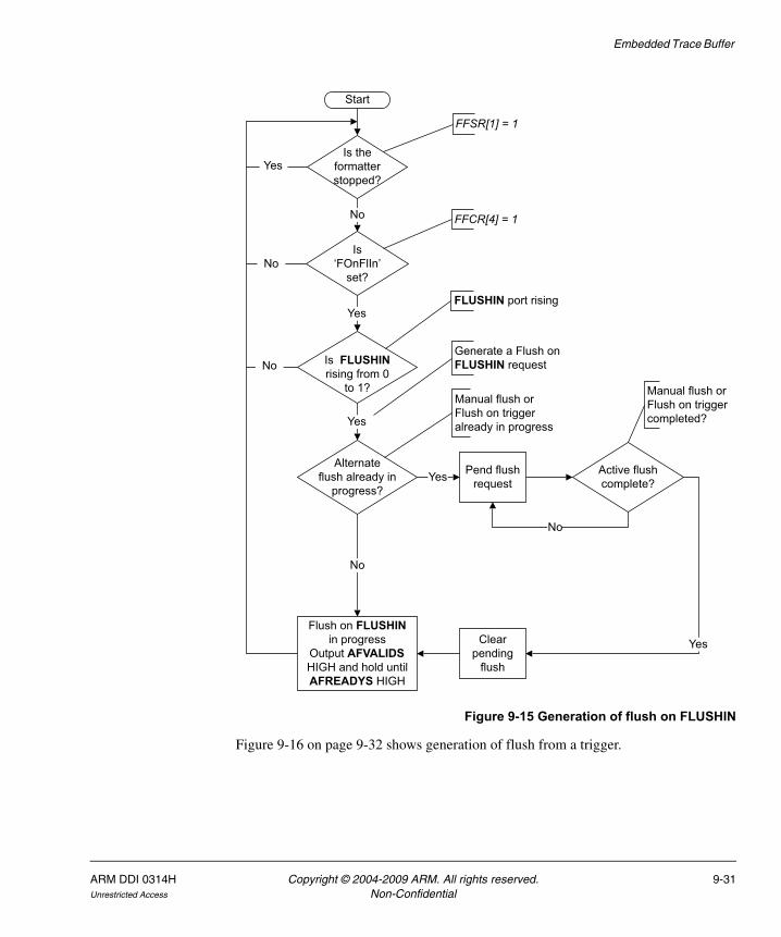
Embedded Trace Buffer
Figure 9-15 Generation of flush on FLUSHIN
Figure 9-16 on page 9-32 shows generation of flush from a trigger.
Start
Is the formatter stopped?
Is ‘FOnFlIn’
set?
Is FLUSHIN rising from 0
to 1?
Alternate flush already in
progress?
Pend flush request
Active flush complete?
Flush on FLUSHIN in progress
Output AFVALIDS HIGH and hold until AFREADYS HIGH
No
Yes
Yes
No
No
Yes
Yes
No
Clear pending
flush
Yes
No
FFSR[1] = 1
FFCR[4] = 1
FLUSHIN port rising
Manual flush or Flush on trigger already in progress
Manual flush or Flush on trigger completed?
Generate a Flush on FLUSHIN request
ARM DDI 0314H Copyright © 2004-2009 ARM. All rights reserved. 9-31Unrestricted Access Non-Confidential
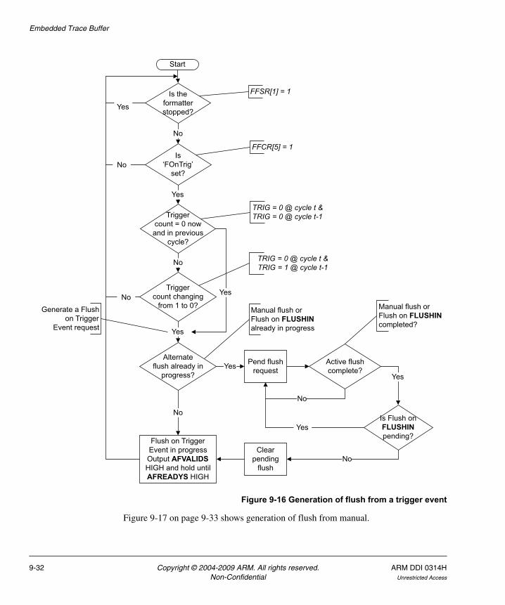
Embedded Trace Buffer
Figure 9-16 Generation of flush from a trigger event
Figure 9-17 on page 9-33 shows generation of flush from manual.
Start
Is the formatter stopped?
Is ‘FOnTrig’
set?
Trigger count = 0 now and in previous
cycle?
Alternate flush already in
progress?
Pend flush request
Active flush complete?
Flush on Trigger Event in progressOutput AFVALIDS HIGH and hold until AFREADYS HIGH
No
Yes
Yes
No
Yes
No
Clear pending
flush
No
FFSR[1] = 1
FFCR[5] = 1
TRIG = 0 @ cycle t & TRIG = 0 @ cycle t-1
Manual flush or Flush on FLUSHIN already in progress
Manual flush or Flush on FLUSHIN completed?
Trigger count changing
from 1 to 0?
Yes
Generate a Flush on Trigger
Event request
TRIG = 0 @ cycle t & TRIG = 1 @ cycle t-1
No
Yes
Is Flush on FLUSHIN pending?
Yes
No
Yes
No
9-32 Copyright © 2004-2009 ARM. All rights reserved. ARM DDI 0314HNon-Confidential Unrestricted Access
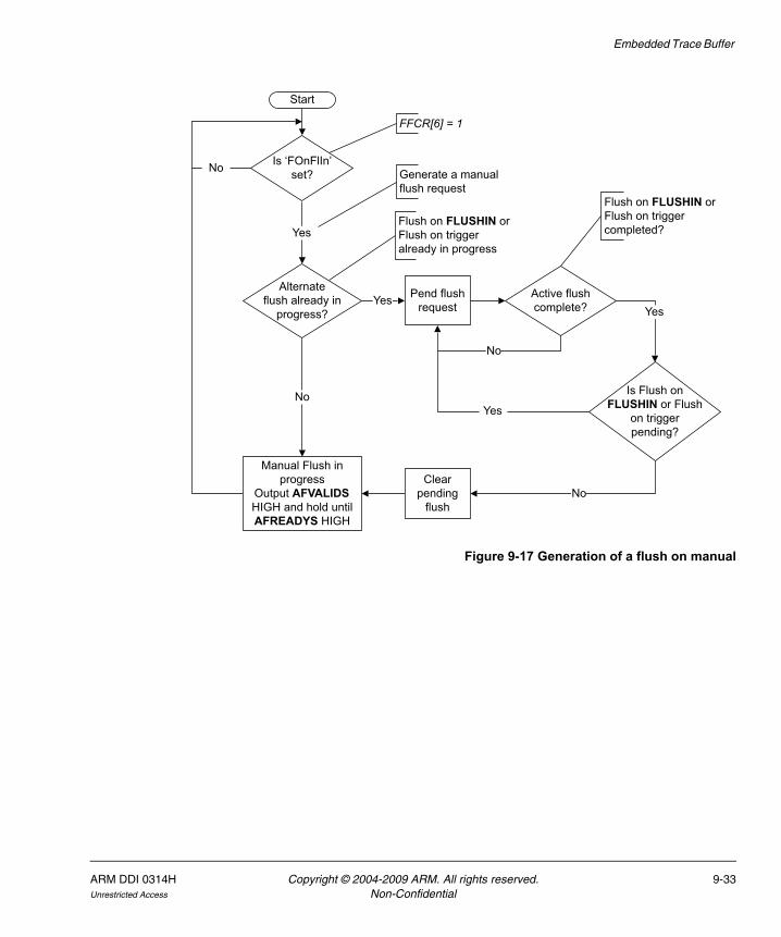
Embedded Trace Buffer
Figure 9-17 Generation of a flush on manual
Start
Is ‘FOnFlIn’ set?No
FFCR[6] = 1
Generate a manual flush request
Alternate flush already in
progress?
Pend flush request
Active flush complete?Yes
No
No
Flush on FLUSHIN or Flush on trigger already in progress
Flush on FLUSHIN or Flush on trigger completed?Yes
Is Flush on FLUSHIN or Flush
on trigger pending?
Yes
Yes
No
Manual Flush in progress
Output AFVALIDS HIGH and hold until AFREADYS HIGH
Clear pending
flush
ARM DDI 0314H Copyright © 2004-2009 ARM. All rights reserved. 9-33Unrestricted Access Non-Confidential
Embedded Trace Buffer
9.8 TriggersA trigger event is defined as when the Trigger Counter reaches zero, or when the trigger counter is zero, when TRIGIN is HIGH. All trigger indication conditions, TrigEvt, TrigFl, and TrigIn, in the Formatter and Flush Control Register can be enabled simultaneously. This results in multiple triggers appearing in the trace stream.
The trigger counter register controls how many words are written into the Trace RAM after a trigger event. After the formatter is flushed in normal or continuous mode a complete empty frame is generated. This is a data overhead of seven extra words in the worst case. The trigger counter defines the number of 32-bit words remaining to be stored in the ETB Trace RAM. If the formatter is in bypass mode, a maximum of two additional words are stored for the trace capture post-amble. See Formatter and Flush Control Register, 0x304 on page 8-17.
Figure 9-18 on page 9-35 shows a flowchart defining the conditions for indicating a trigger in the formatted data. This flowchart only applies for the condition when continuous formatting is enabled (EnFCont HIGH) in the Formatter and Flush Control Register.
9-34 Copyright © 2004-2009 ARM. All rights reserved. ARM DDI 0314HNon-Confidential Unrestricted Access
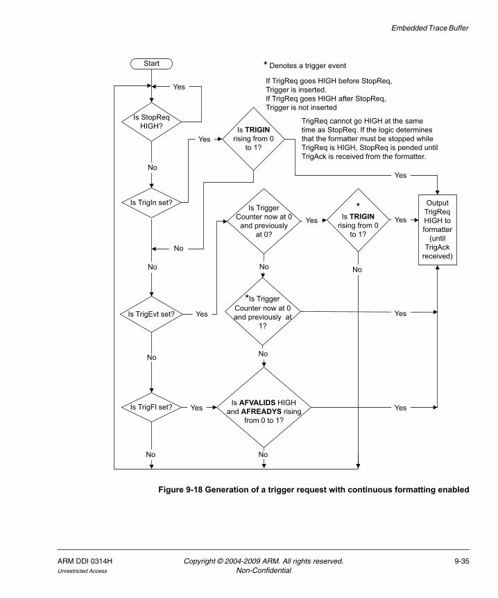
Embedded Trace Buffer
Figure 9-18 Generation of a trigger request with continuous formatting enabled
Is TRIGIN rising from 0
to 1?
Is Trigger Counter now at 0
and previously at 0?
*Is Trigger Counter now at 0 and previously at
1?
*Is TRIGIN
rising from 0 to 1?
Output TrigReq HIGH to formatter
(until TrigAck
received)No
Yes
No No
No
No
Is AFVALIDS HIGH and AFREADYS rising
from 0 to 1?
No
No
No
Yes
Yes
Yes
Yes
Yes
No
Is TrigIn set?
Is TrigEvt set?
Start
Is TrigFl set?
Is StopReq HIGH?
Yes
Yes
Yes
If TrigReq goes HIGH before StopReq,Trigger is inserted.If TrigReq goes HIGH after StopReq,Trigger is not inserted
* Denotes a trigger event
TrigReq cannot go HIGH at the same time as StopReq. If the logic determines that the formatter must be stopped while TrigReq is HIGH, StopReq is pended until TrigAck is received from the formatter.
ARM DDI 0314H Copyright © 2004-2009 ARM. All rights reserved. 9-35Unrestricted Access Non-Confidential

Embedded Trace Buffer
9.9 Write address generation for trace data storageThe RAM Write Pointer is automatically selected for addressing the Trace RAM when trace capture is enabled in the Control Register. Data is written into the Trace RAM when the formatter asserts the DataValid flag on generation of a formatted word. On completion of a write access to the Trace RAM the register is automatically incremented.
The RAM Write Pointer Register must be programmed before trace capture is enabled.
9-36 Copyright © 2004-2009 ARM. All rights reserved. ARM DDI 0314HNon-Confidential Unrestricted Access
Embedded Trace Buffer
9.10 Trace data storageData is received by the ETB ATB Formatter block. When TraceCaptEn is asserted the Formatter starts the process of embedding the source IDs into the data stream, or normal mode, then outputs 32-bit words to be stored in the ETB Trace RAM. When data is ready to be stored in the Trace RAM, data is written to at the address stored in the RAM Write Pointer Register. When the Trigger Counter Register reaches zero, the acquisition complete flag AcqComp is asserted and trace capture is stopped.
ARM DDI 0314H Copyright © 2004-2009 ARM. All rights reserved. 9-37Unrestricted Access Non-Confidential
Embedded Trace Buffer
9.11 APB configuration and RAM accessThis section describes APB configuration and RAM accesses:
• Read access
• Write access.
9.11.1 Read access
When trace capture is disabled (TraceCaptEn=0), the RAM Read Pointer is used to generate the RAM address for reading data stored in the ETB Trace RAM. Updating the RAM Read Pointer automatically triggers a RAM access to ensure all RAM data present in the RAM Read Data Register is up-to-date.
The RAM Read Pointer is updated either by writing directly to it, or performing a read of the RAM Read Data Register, causing the RAM Read Pointer to be incremented. Therefore, a read of the RAM Read Data Register consequentially causes the next memory location to be read and loaded into the RAM Read Data Register.
9.11.2 Write access
When trace capture is disabled (TraceCaptEn=0), the RAM Write Pointer Register is used to generate the RAM address for writing data from the RAM Read Data Register. Compare this with trace capture is enabled, and trace data storage from the ATB interface. The data to be stored in the RAM Write Data Register is derived from an APB write transfer to the APB interface.
Updating the RAM Read Data Register automatically triggers a RAM access to write the register contents into the Trace RAM at the address present in the RAM Write Pointer Register. On completion of the write cycle the RAM Write Pointer Register is automatically incremented.
Note A write access to the RAM Write Pointer Register does not initiate a write transfer to the Trace RAM, only a write to the RAM Read Data Register causes a RAM write.
The RAM Write Pointer Register must be programmed before trace capture is re-enabled.
9-38 Copyright © 2004-2009 ARM. All rights reserved. ARM DDI 0314HNon-Confidential Unrestricted Access
Embedded Trace Buffer
9.12 Trace RAMSee the CoreSight Components Implementation Guide for information about Trace RAM and RAM integration.
ARM DDI 0314H Copyright © 2004-2009 ARM. All rights reserved. 9-39Unrestricted Access Non-Confidential
Embedded Trace Buffer
9.13 Authentication requirements for CoreSight ETBsCoreSight ETBs do not require any inputs capable of disabling them.
9-40 Copyright © 2004-2009 ARM. All rights reserved. ARM DDI 0314HNon-Confidential Unrestricted Access
Embedded Trace Buffer
9.14 ETB RAM supportThe ETB RAM support is described in:
• Access sizes
• BIST interface
• RAM instantiation.
9.14.1 Access sizes
Byte writable RAMs are not supported. Trace storage is only in word accesses, and APB accesses take place through the RAM Write Data Register, again 32 bits. The APB interface has no concept of data size.
9.14.2 BIST interface
The RAM BIST interface connects though the Trace RAM Interface block to provide test access to the Trace RAM. MTESTON enables the memory BIST interface and disables all other accesses to and from the RAM.
9.14.3 RAM instantiation
As shown in Figure 9-19, the CSEtbRam block provides the wrapper in which the RAM simulation model/hardened cell can be instantiated. The active level of Chip Enable, Write Enable can be modified in this block.
Figure 9-19 ETB trace RAM block wrapper
AMBISTADDR
DINMBISTDIN
CSMBISTCE
WEMBISTWEMTESTON
CLK
ETBMBISTDOUT
CSEtbramA
DIN
CS
WE
CLK
DOUT
ARM DDI 0314H Copyright © 2004-2009 ARM. All rights reserved. 9-41Unrestricted Access Non-Confidential
Embedded Trace Buffer
9.15 ETB configuration optionsThis section describes:
• ETM architecture version no longer required
• RAM options.
9.15.1 ETM architecture version no longer required
ETM architecture version configuration is no longer required on the Formatter input. The ETB is now trace data agnostic, with formatting carried out in a consistent manner, with optional bypass, as defined in the CoreSight Architecture Specification.
9.15.2 RAM options
RAM width is 32 bits. This minimizes buffering in the formatter and ensures that the Trace RAM can be used as slow software-accessible memory.
The RAM depth is configurable by setting the address bus width using CSETB_RAM_ADRW, as shown in Table 9-23. Previous implementations of the ETB did not specify a lower and upper range of RAM configurations. ARM currently recommends customers adopt a minimum RAM size of 4KB. The range specified covers both ends of requirements, and meets future trace storage requirements.
Table 9-23 ETB RAM size options
Address range Words stored Total storage in KB
[7:0] 256 1
[8:0] 512 2
[9:0] 1024 4
[10:0] 2048 8
[11:0] 4096 16
[12:0] 8192 32
[13:0] 16384 64
[14:0] 32768 128
[15:0] 65536 256
[16:0] 131072 512
[17:0] 262144 1024
9-42 Copyright © 2004-2009 ARM. All rights reserved. ARM DDI 0314HNon-Confidential Unrestricted Access
Embedded Trace Buffer
9.16 Comparisons with ETB11Table 9-24 shows the differences and similarities between ETB11 and CoreSight ETB.
Table 9-24 ETB11 and ETB comparison
ETB11 feature Changes in ETB Comments References
JTAG Port Does not exist Access is through a single APB bus for memory access and configuration
ATB interface on page 9-3.
Programmers Model Integration into standard PrimeCell peripheral ID register structure
Existing registers maintain their current location where required
ETB register descriptions on page 9-8.
Existing registers are modified to support the peripheral ID register structure where required
ETB register descriptions on page 9-8.
AHB Interface Port is replaced with an AMBA 3 APB interface
Trace RAM is no longer memory-mapped.
ATB interface on page 9-3.
Access is through a single APB bus for memory access and configuration
ETM Trace Interface Replacement with an ATB-compliant trace input
- See ETB Trace capture and formatting on page 9-25.
Replacement of the Data Formatter block with CoreSight-compliant formatter unit
-
ETB Trace RAM Support for 32-bit RAM only
- -
Word-width access only required.
- -
Direct RAM access removed.
- -
Use of read and write register pointers, with auto-incrementing addresses, like the original JTAG access methodology
- -
ARM DDI 0314H Copyright © 2004-2009 ARM. All rights reserved. 9-43Unrestricted Access Non-Confidential

Embedded Trace Buffer
9-44 Copyright © 2004-2009 ARM. All rights reserved. ARM DDI 0314HNon-Confidential Unrestricted Access
Chapter 10 Serial Wire Viewer
This chapter describes the Serial Wire Viewer (SWV). It contains the following sections:
• About the Serial Wire Viewer on page 10-2
• SWV interfaces on page 10-3
• Authentication requirements on page 10-5.
ARM DDI 0314H Copyright © 2004-2009 ARM. All rights reserved. 10-1Unrestricted Access Non-Confidential
Serial Wire Viewer
10.1 About the Serial Wire ViewerThe Instrumentation Trace Macrocell (ITM) and Serial Wire Output (SWO) can be used to form a SWV, as shown in Figure 10-1.
Figure 10-1 ITM and SWO as part of a SWV system
When the ITM and SWO are used as part of the SWV:
• if PADDRDBG[12] is set LOW, the ITM registers are accessed
• if PADDRDBG[12] is set HIGH, the SWO registers are accessed.
The ATIDM and AFREADYM outputs from the ITM are left unconnected. These signals are not required for the connection to SWO. Because of this, it is not necessary to write to the ITM Integration Register, ITATBCTR1, for integration testing against the SWO.
Note For more information on the ITM and SWO, see Chapter 12 Instrumentation Trace Macrocell and Chapter 11 Serial Wire Output.
ITM SWO
APB mux
ATB TRACESWO
SWV
APB
10-2 Copyright © 2004-2009 ARM. All rights reserved. ARM DDI 0314HNon-Confidential Unrestricted Access
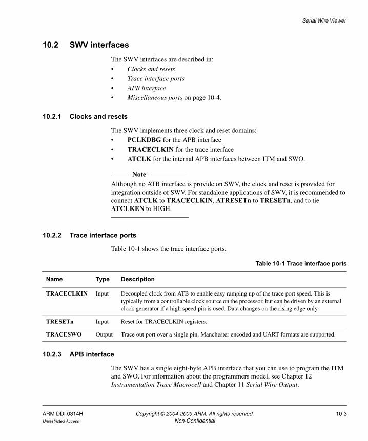
Serial Wire Viewer
10.2 SWV interfacesThe SWV interfaces are described in:
• Clocks and resets
• Trace interface ports
• APB interface
• Miscellaneous ports on page 10-4.
10.2.1 Clocks and resets
The SWV implements three clock and reset domains:
• PCLKDBG for the APB interface
• TRACECLKIN for the trace interface
• ATCLK for the internal APB interfaces between ITM and SWO.
Note Although no ATB interface is provide on SWV, the clock and reset is provided for integration outside of SWV. For standalone applications of SWV, it is recommended to connect ATCLK to TRACECLKIN, ATRESETn to TRESETn, and to tie ATCLKEN to HIGH.
10.2.2 Trace interface ports
Table 10-1 shows the trace interface ports.
10.2.3 APB interface
The SWV has a single eight-byte APB interface that you can use to program the ITM and SWO. For information about the programmers model, see Chapter 12 Instrumentation Trace Macrocell and Chapter 11 Serial Wire Output.
Table 10-1 Trace interface ports
Name Type Description
TRACECLKIN Input Decoupled clock from ATB to enable easy ramping up of the trace port speed. This is typically from a controllable clock source on the processor, but can be driven by an external clock generator if a high speed pin is used. Data changes on the rising edge only.
TRESETn Input Reset for TRACECLKIN registers.
TRACESWO Output Trace out port over a single pin. Manchester encoded and UART formats are supported.
ARM DDI 0314H Copyright © 2004-2009 ARM. All rights reserved. 10-3Unrestricted Access Non-Confidential
Serial Wire Viewer
When the ITM and SWO are used as part of the SWV:
• if PADDRDBG[12] is set LOW, the ITM registers are accessed
• if PADDRDBG[12] is set HIGH, the SWO registers are accessed.
10.2.4 Miscellaneous ports
Table 10-2 shows the miscellaneous SWV ports.
Table 10-2 Miscellaneous ports
Name Type Description
TRIGOUT Output Indicates a trigger event, that is, a write to a stimulus register that has a trigger enable against it
TRIGOUTACK Input Asynchronous TRIGOUT acknowledgement signal
10-4 Copyright © 2004-2009 ARM. All rights reserved. ARM DDI 0314HNon-Confidential Unrestricted Access
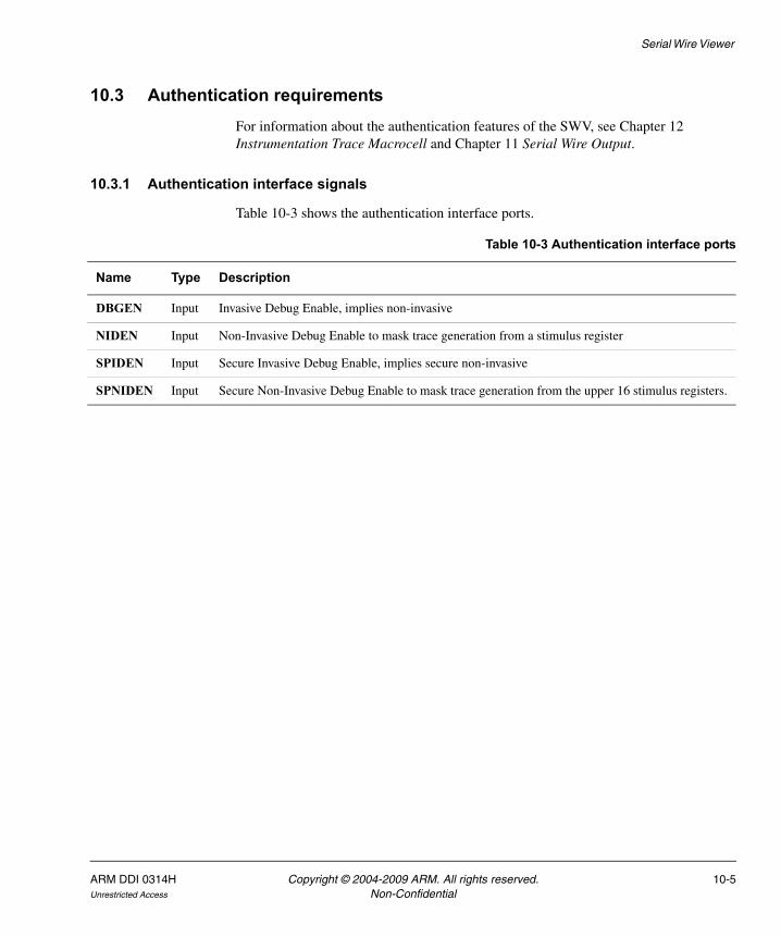
Serial Wire Viewer
10.3 Authentication requirementsFor information about the authentication features of the SWV, see Chapter 12 Instrumentation Trace Macrocell and Chapter 11 Serial Wire Output.
10.3.1 Authentication interface signals
Table 10-3 shows the authentication interface ports.
Table 10-3 Authentication interface ports
Name Type Description
DBGEN Input Invasive Debug Enable, implies non-invasive
NIDEN Input Non-Invasive Debug Enable to mask trace generation from a stimulus register
SPIDEN Input Secure Invasive Debug Enable, implies secure non-invasive
SPNIDEN Input Secure Non-Invasive Debug Enable to mask trace generation from the upper 16 stimulus registers.
ARM DDI 0314H Copyright © 2004-2009 ARM. All rights reserved. 10-5Unrestricted Access Non-Confidential

Serial Wire Viewer
10-6 Copyright © 2004-2009 ARM. All rights reserved. ARM DDI 0314HNon-Confidential Unrestricted Access
Chapter 11 Serial Wire Output
This chapter describes the Serial Wire Output (SWO). It contains the following sections:
• About the Serial Wire Output on page 11-2
• SWO ports on page 11-3
• SWO programmers model on page 11-4
• CoreSight defined registers on page 11-6
• Trace port control registers on page 11-9
• Trigger registers on page 11-11
• EXTCTL registers on page 11-12
• Test pattern registers on page 11-13
• Formatter and flush registers on page 11-14
• Integration test registers on page 11-16
• SWO trace port on page 11-18.
ARM DDI 0314H Copyright © 2004-2009 ARM. All rights reserved. 11-1Unrestricted Access Non-Confidential
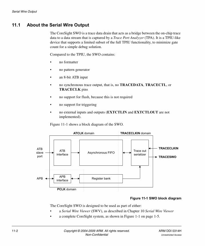
Serial Wire Output
11.1 About the Serial Wire OutputThe CoreSight SWO is a trace data drain that acts as a bridge between the on-chip trace data to a data stream that is captured by a Trace Port Analyzer (TPA). It is a TPIU-like device that supports a limited subset of the full TPIU functionality, to minimize gate count for a simple debug solution.
Compared to the TPIU, the SWO contains:
• no formatter
• no pattern generator
• an 8-bit ATB input
• no synchronous trace output, that is, no TRACEDATA, TRACECTL, or TRACECLK pins
• no support for flush, because this is not required
• no support for triggering
• no external inputs and outputs (EXTCTLIN and EXTCTLOUT are not implemented).
Figure 11-1 shows a block diagram of the SWO.
Figure 11-1 SWO block diagram
The CoreSight SWO is designed to be used as part of either:
• a Serial Wire Viewer (SWV), as described in Chapter 10 Serial Wire Viewer
• a complete CoreSight system, as shown in Figure 1-1 on page 1-5.
ATB interface
APB interface Register bank
Asynchronous FIFO Trace out serializer
ATB slave port
APB
TRACECLKIN
TRACESWO
ATCLK domain TRACECLKIN domain
PCLK domain
11-2 Copyright © 2004-2009 ARM. All rights reserved. ARM DDI 0314HNon-Confidential Unrestricted Access
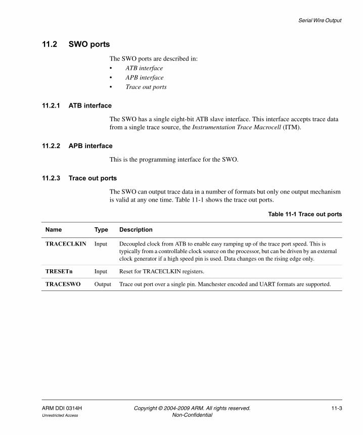
Serial Wire Output
11.2 SWO portsThe SWO ports are described in:
• ATB interface
• APB interface
• Trace out ports
11.2.1 ATB interface
The SWO has a single eight-bit ATB slave interface. This interface accepts trace data from a single trace source, the Instrumentation Trace Macrocell (ITM).
11.2.2 APB interface
This is the programming interface for the SWO.
11.2.3 Trace out ports
The SWO can output trace data in a number of formats but only one output mechanism is valid at any one time. Table 11-1 shows the trace out ports.
Table 11-1 Trace out ports
Name Type Description
TRACECLKIN Input Decoupled clock from ATB to enable easy ramping up of the trace port speed. This is typically from a controllable clock source on the processor, but can be driven by an external clock generator if a high speed pin is used. Data changes on the rising edge only.
TRESETn Input Reset for TRACECLKIN registers.
TRACESWO Output Trace out port over a single pin. Manchester encoded and UART formats are supported.
ARM DDI 0314H Copyright © 2004-2009 ARM. All rights reserved. 11-3Unrestricted Access Non-Confidential
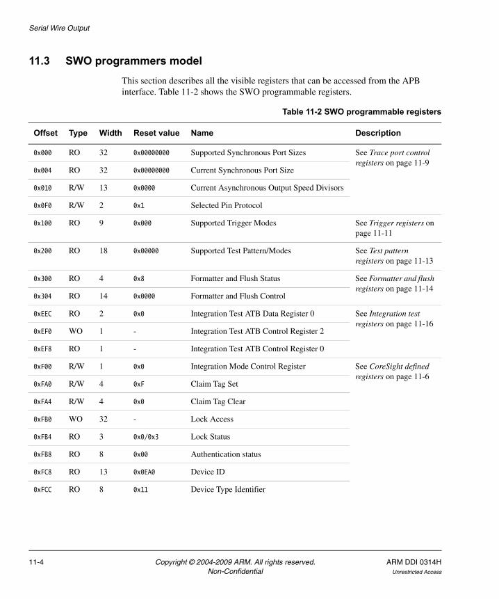
Serial Wire Output
11.3 SWO programmers modelThis section describes all the visible registers that can be accessed from the APB interface. Table 11-2 shows the SWO programmable registers.
Table 11-2 SWO programmable registers
Offset Type Width Reset value Name Description
0x000 RO 32 0x00000000 Supported Synchronous Port Sizes See Trace port control registers on page 11-9
0x004 RO 32 0x00000000 Current Synchronous Port Size
0x010 R/W 13 0x0000 Current Asynchronous Output Speed Divisors
0x0F0 R/W 2 0x1 Selected Pin Protocol
0x100 RO 9 0x000 Supported Trigger Modes See Trigger registers on page 11-11
0x200 RO 18 0x00000 Supported Test Pattern/Modes See Test pattern registers on page 11-13
0x300 RO 4 0x8 Formatter and Flush Status See Formatter and flush registers on page 11-14
0x304 RO 14 0x0000 Formatter and Flush Control
0xEEC RO 2 0x0 Integration Test ATB Data Register 0 See Integration test registers on page 11-16
0xEF0 WO 1 - Integration Test ATB Control Register 2
0xEF8 RO 1 - Integration Test ATB Control Register 0
0xF00 R/W 1 0x0 Integration Mode Control Register See CoreSight defined registers on page 11-6
0xFA0 R/W 4 0xF Claim Tag Set
0xFA4 R/W 4 0x0 Claim Tag Clear
0xFB0 WO 32 - Lock Access
0xFB4 RO 3 0x0/0x3 Lock Status
0xFB8 RO 8 0x00 Authentication status
0xFC8 RO 13 0x0EA0 Device ID
0xFCC RO 8 0x11 Device Type Identifier
11-4 Copyright © 2004-2009 ARM. All rights reserved. ARM DDI 0314HNon-Confidential Unrestricted Access
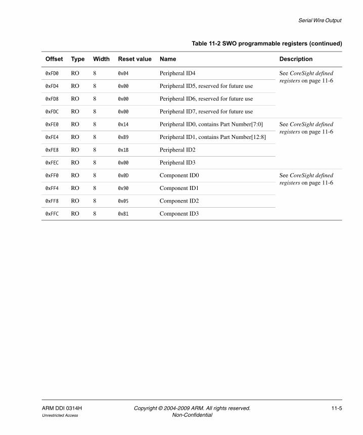
Serial Wire Output
0xFD0 RO 8 0x04 Peripheral ID4 See CoreSight defined registers on page 11-6
0xFD4 RO 8 0x00 Peripheral ID5, reserved for future use
0xFD8 RO 8 0x00 Peripheral ID6, reserved for future use
0xFDC RO 8 0x00 Peripheral ID7, reserved for future use
0xFE0 RO 8 0x14 Peripheral ID0, contains Part Number[7:0] See CoreSight defined registers on page 11-6
0xFE4 RO 8 0xB9 Peripheral ID1, contains Part Number[12:8]
0xFE8 RO 8 0x1B Peripheral ID2
0xFEC RO 8 0x00 Peripheral ID3
0xFF0 RO 8 0x0D Component ID0 See CoreSight defined registers on page 11-6
0xFF4 RO 8 0x90 Component ID1
0xFF8 RO 8 0x05 Component ID2
0xFFC RO 8 0xB1 Component ID3
Table 11-2 SWO programmable registers (continued)
Offset Type Width Reset value Name Description
ARM DDI 0314H Copyright © 2004-2009 ARM. All rights reserved. 11-5Unrestricted Access Non-Confidential
Serial Wire Output
11.4 CoreSight defined registersThese registers are described the CoreSight Architecture Specification. This section describes the values that are specific to the SWO:
• Integration Mode Control Register, 0xF00 [0]
• Claim Tag Set and Clear Registers, 0xFA0 [3:0] and 0xFA4 [3:0]
• Lock Access Register, 0xFB0 [31:0]
• Lock Status Register, 0xFB4 [2:0]
• SWO identification registers on page 11-7.
11.4.1 Integration Mode Control Register, 0xF00 [0]
This register enables the device to switch from a functional mode, or default behavior, into integration mode where the device inputs and outputs can be directly controlled for the purpose of integration testing/topology solving. For the SWO, it is set to 0x1 to enable Integration mode.
11.4.2 Claim Tag Set and Clear Registers, 0xFA0 [3:0] and 0xFA4 [3:0]
Typically these registers enable the sharing of resources. The SWO has no resources to share, and has a claim tag of 4 bits.
11.4.3 Lock Access Register, 0xFB0 [31:0]
The Lock Access Register is write-only. This register enables write access to component registers. A write of 0xC5ACCE55 enables further write access to this component. An invalid write has the effect of removing write access. This Lock Access Mechanism can be bypassed by setting PADDRDBG31, the highest APB Address line, to HIGH. In this case, the entire device can be accessed.
11.4.4 Lock Status Register, 0xFB4 [2:0]
The Lock Status Register indicates the status of the lock control mechanism, and is used in conjunction with the Lock Access Register.
11-6 Copyright © 2004-2009 ARM. All rights reserved. ARM DDI 0314HNon-Confidential Unrestricted Access
Serial Wire Output
Table 11-3 shows the bit assignments.
Note When PADDRDBG31 is HIGH, the Lock Access Mechanism is bypassed and the Lock Status Register does not reflect the actual status of the Lock Access, and the register reads zero.
11.4.5 SWO identification registers
The identification register values specific to the SWO are:
Authentication Status Register, 0xFB8 [7:0]
This register reports the required security level for operation, and is set to 0x00 for functionality not implemented.
Device ID, 0xFC8
Table 11-4 shows the SWO Device ID Register bit assignments.
Table 11-3 Lock Status Register bit assignments
Bits Name Description
[31:3] - Reserved RAZ/SBZP.
[2] 8-BIT Access Lock Register size. This bit reads 0 to indicate a 32-bit register is present.
[1] STATUS Lock Status. This bit is HIGH when the device is locked, and LOW when unlocked.
[0] IMP Lock mechanism is implemented. This bit always reads 1.
Table 11-4 Device ID Register bit assignments
Bits Value Description
[31:12] 0x00000 Reserved RAZ/SBZP.
[11] 1 UART/NRZ Serial Wire Output supported.
[10] 1 Manchester Serial Wire Output supported.
[9] 1 Synchronous trace port (trace clock and data) not supported.
ARM DDI 0314H Copyright © 2004-2009 ARM. All rights reserved. 11-7Unrestricted Access Non-Confidential
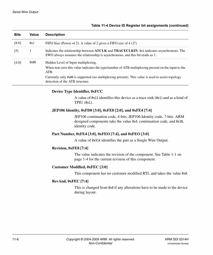
Serial Wire Output
Device Type Identifier, 0xFCC
A value of 0x11 identifies this device as a trace sink (0x1) and as a kind of TPIU (0x1).
JEP106 Identity, 0xFD0 [3:0], 0xFE8 [2:0], and 0xFE4 [7:4]
JEP106 continuation code, 4-bits, JEP106 Identity code, 7-bits. ARM designed components take the value 0x4, continuation code, and 0x3B, identity code.
Part Number, 0xFE4 [3:0], 0xFEO [7:4], and 0xFEO [3:0]
A value of 0x914 identifies the part as a Single Wire Output.
Revision, 0xFE8 [7:4]
The value indicates the revision of the component. See Table 1-1 on page 1-4 for the current revision of this component.
Customer Modified, 0xFEC [3:0]
This component has no customer modified RTL and takes the value 0x0.
RevAnd, 0xFEC [7:4]
This is changed from 0x0 if any alterations have to be made to the device during layout.
[8:6] 0x2 FIFO Size (Power of 2). A value of 2 gives a FIFO size of 4 (22).
[5] 1 Indicates the relationship between ATCLK and TRACECLKIN. 0x1 indicates asynchronous. The SWO always assumes the relationship is asynchronous, and this bit reads as 1.
[4:0] 0x00 Hidden Level of Input multiplexing.
When non-zero this value indicates the type/number of ATB multiplexing present on the input to the ATB.
Currently only 0x00 is supported (no multiplexing present). This value is used to assist topology detection of the ATB structure.
Table 11-4 Device ID Register bit assignments (continued)
Bits Value Description
11-8 Copyright © 2004-2009 ARM. All rights reserved. ARM DDI 0314HNon-Confidential Unrestricted Access
Serial Wire Output
11.5 Trace port control registersThis section describes the trace port control registers:
• Supported Synchronous Port Size Register, SPR, 0x000
• Current Synchronous Port Size Register, CPR, 0x004
• Current Output Divisor Register, CODR, 0x010
• Selected Pin Protocol Register, SPPR, 0xF0 on page 11-10.
Note For more information on the trace port, see SWO trace port on page 11-18.
11.5.1 Supported Synchronous Port Size Register, SPR, 0x000
The SWO does not support synchronous mode, so this register reads as zero.
11.5.2 Current Synchronous Port Size Register, CPR, 0x004
The SWO does not support synchronous mode, so this register reads as zero.
11.5.3 Current Output Divisor Register, CODR, 0x010
With this register is possible to scale the baud rate of the SWO output. It divides TRACECLKIN, enabling it when the counter reaches the programmed value, and reducing the baud rate of the TRACESWO pin. Its reset value is 0x0000 and the counter is always running. The actual division value for the TRACECLKIN frequency is the value of this register plus one.
Whenever this register is reprogrammed, the internal counter is automatically reset, making the baud-rate change instantaneously.
Note • The SWO does not support stopping. Changing the prescaler while trace is being
processed is permitted. However, the moment of change in relation to the trace port is unpredictable. It is recommended that the trace source is disabled, and the trace port idle, before changing this register.
• When the Divisor field has been altered, the capture device must also be adjusted where appropriate to ensure the correct data is captured.
Figure 11-2 on page 11-10 shows the Current Output Divisor Register bit assignments.
ARM DDI 0314H Copyright © 2004-2009 ARM. All rights reserved. 11-9Unrestricted Access Non-Confidential
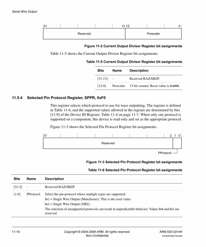
Serial Wire Output
Figure 11-2 Current Output Divisor Register bit assignments
Table 11-5 shows the Current Output Divisor Register bit assignments.
11.5.4 Selected Pin Protocol Register, SPPR, 0xF0
This register selects which protocol to use for trace outputting. The register is defined in Table 11-6, and the supported values allowed in the register are determined by bits [11:9] of the Device ID Register, Table 11-4 on page 11-7. When only one protocol is supported on a component, this device is read only and set as the appropriate protocol.
Figure 11-3 shows the Selected Pin Protocol Register bit assignments.
Figure 11-3 Selected Pin Protocol Register bit assignments
Reserved
31 13 12 0
Prescaler
Table 11-5 Current Output Divisor Register bit assignments
Bits Name Description
[31:13] - Reserved RAZ/SBZP.
[12:0] Prescaler 13 bit counter. Reset value is 0x0000.
Table 11-6 Selected Pin Protocol Register bit assignments
Bits Name Description
[31:2] - Reserved RAZ/SBZP.
[1:0] PProtocol Select the pin protocol where multiple types are supported:
0x1 = Single Wire Output (Manchester). This is the reset value.
0x2 = Single Wire Output (NRZ).
The selection of unsupported protocols can result in unpredictable behavior. Values 0x0 and 0x3 are reserved.
Reserved
31 2 1 0
PProtocol
11-10 Copyright © 2004-2009 ARM. All rights reserved. ARM DDI 0314HNon-Confidential Unrestricted Access
Serial Wire Output
11.6 Trigger registersTriggering is not supported in the SWO. For those trigger registers not present, read attempts return 0x00000000 and writes are ignored.
11.6.1 Supported Trigger Mode Register, STMR, 0x100
This register indicates the implemented Trigger Counter multipliers and other supported features of the trigger system. Because no trigger options are implemented in the SWO, this register reads as zero.
ARM DDI 0314H Copyright © 2004-2009 ARM. All rights reserved. 11-11Unrestricted Access Non-Confidential
Serial Wire Output
11.7 EXTCTL registersExternal control inputs and outputs are not implemented in the SWO. Read attempts to these registers, EXTCTLIN and EXTCTLOUT, return 0x00000000 and writes are ignored.
11-12 Copyright © 2004-2009 ARM. All rights reserved. ARM DDI 0314HNon-Confidential Unrestricted Access
Serial Wire Output
11.8 Test pattern registersThe test pattern generator is not implemented in the SWO. For those test pattern registers not present, read attempts return 0x00000000 and writes are ignored.
11.8.1 Supported Test Patterns and Modes Register, STPR, 0x200
This register indicates the implemented test patterns and modes in the SWO. It reads as zero because no pattern modes or test patterns are available in the SWO.
ARM DDI 0314H Copyright © 2004-2009 ARM. All rights reserved. 11-13Unrestricted Access Non-Confidential
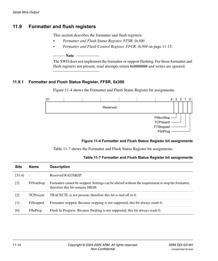
Serial Wire Output
11.9 Formatter and flush registersThis section describes the formatter and flush registers:
• Formatter and Flush Status Register, FFSR, 0x300
• Formatter and Flush Control Register, FFCR, 0x304 on page 11-15.
Note The SWO does not implement the formatter or support flushing. For those formatter and flush registers not present, read attempts return 0x00000000 and writes are ignored.
11.9.1 Formatter and Flush Status Register, FFSR, 0x300
Figure 11-4 shows the Formatter and Flush Status Register bit assignments.
Figure 11-4 Formatter and Flush Status Register bit assignments
Table 11-7 shows the Formatter and Flush Status Register bit assignments.
Reserved
31 4 3 2 1 0
FtNonStopTCPresentFTStopped
FlInProg
Table 11-7 Formatter and Flush Status Register bit assignments
Bits Name Description
[31:4] - Reserved RAZ/SBZP.
[3] FtNonStop Formatter cannot be stopped. Settings can be altered without the requirement to stop the formatter, therefore this bit remains HIGH.
[2] TCPresent TRACECTL is not present, therefore this bit is tied off to 0.
[1] FtStopped Formatter stopped. Because stopping is not supported, this bit always reads 0.
[0] FlInProg Flush In Progress. Because flushing is not supported, this bit always reads 0.
11-14 Copyright © 2004-2009 ARM. All rights reserved. ARM DDI 0314HNon-Confidential Unrestricted Access
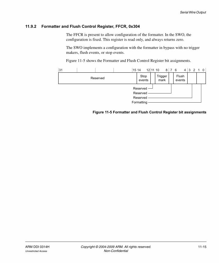
Serial Wire Output
11.9.2 Formatter and Flush Control Register, FFCR, 0x304
The FFCR is present to allow configuration of the formatter. In the SWO, the configuration is fixed. This register is read only, and always returns zero.
The SWO implements a configuration with the formatter in bypass with no trigger makers, flush events, or stop events.
Figure 11-5 shows the Formatter and Flush Control Register bit assignments.
Figure 11-5 Formatter and Flush Control Register bit assignments
Reserved
31 14 12 11 10 8 7 6 4 3 2 1 0
Stop events
Trigger mark
Flush events
ReservedReservedReserved
15
Formatting
ARM DDI 0314H Copyright © 2004-2009 ARM. All rights reserved. 11-15Unrestricted Access Non-Confidential
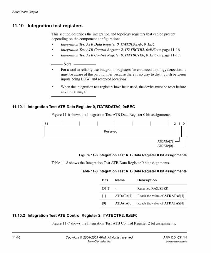
Serial Wire Output
11.10 Integration test registersThis section describes the integration and topology registers that can be present depending on the component configuration:
• Integration Test ATB Data Register 0, ITATBDATA0, 0xEEC
• Integration Test ATB Control Register 2, ITATBCTR2, 0xEF0 on page 11-16
• Integration Test ATB Control Register 0, ITATBCTR0, 0xEF8 on page 11-17.
Note • For a tool to reliably use integration registers for enhanced topology detection, it
must be aware of the part number because there is no way to distinguish between inputs being LOW, and reserved locations.
• When the integration test registers have been used, the device must be reset before any more usage.
11.10.1 Integration Test ATB Data Register 0, ITATBDATA0, 0xEEC
Figure 11-6 shows the Integration Test ATB Data Register 0 bit assignments.
Figure 11-6 Integration Test ATB Data Register 0 bit assignments
Table 11-8 shows the Integration Test ATB Data Register 0 bit assignments.
11.10.2 Integration Test ATB Control Register 2, ITATBCTR2, 0xEF0
Figure 11-7 shows the Integration Test ATB Control Register 2 bit assignments.
Reserved
31 2 1 0
ATDATA[7]ATDATA[0]
Table 11-8 Integration Test ATB Data Register 0 bit assignments
Bits Name Description
[31:2] - Reserved RAZ/SBZP.
[1] ATDATA[7] Reads the value of ATDATAS[7]
[0] ATDATA[0] Reads the value of ATDATAS[0]
11-16 Copyright © 2004-2009 ARM. All rights reserved. ARM DDI 0314HNon-Confidential Unrestricted Access
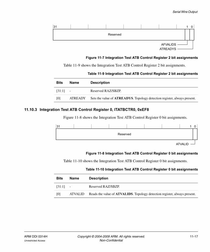
Serial Wire Output
Figure 11-7 Integration Test ATB Control Register 2 bit assignments
Table 11-9 shows the Integration Test ATB Control Register 2 bit assignments.
11.10.3 Integration Test ATB Control Register 0, ITATBCTR0, 0xEF8
Figure 11-8 shows the Integration Test ATB Control Register 0 bit assignments.
Figure 11-8 Integration Test ATB Control Register 0 bit assignments
Table 11-10 shows the Integration Test ATB Control Register 0 bit assignments.
31
Reserved
01
AFVALIDSATREADYS
Table 11-9 Integration Test ATB Control Register 2 bit assignments
Bits Name Description
[31:1] - Reserved RAZ/SBZP.
[0] ATREADY Sets the value of ATREADYS. Topology detection register, always present.
Reserved
31 1 0
ATVALID
Table 11-10 Integration Test ATB Control Register 0 bit assignments
Bits Name Description
[31:1] - Reserved RAZ/SBZP.
[0] ATVALID Reads the value of ATVALIDS. Topology detection register, always present.
ARM DDI 0314H Copyright © 2004-2009 ARM. All rights reserved. 11-17Unrestricted Access Non-Confidential
Serial Wire Output
11.11 SWO trace portThis section contains additional information about output port sizes and modes:
• Supported port sizes
• Physical pin protocol.
11.11.1 Supported port sizes
Both asynchronous port modes only operate over a single pin, TRACESWO, and do not require separate clock or control pins. Although data is output over a single pin, every data packet is in 8-bit multiples (bytes) when either the Manchester or UART pin protocols are selected.
11.11.2 Physical pin protocol
For a trace capture device to correctly interpret trace data from a SWO, it must know how to decode where data exists on the various pin protocols. This section describes how logic is interpreted and any wire protocols that must be decoded to establish the underlying transmit data.
Note In Table 11-11 on page 11-19 and Table 11-12 on page 11-20, the terms HIGH and LOW are relative terms that describe how the pin can appear electrically:
• LOW is typically 0V
• HIGH is equivalent to the supply voltage.
Two types of encoding are used:
• Manchester encoding
• UART encoding on page 11-19.
Manchester encoding
This protocol is supported if bit [10] of the Device ID Register, 0xFC8, is set. It is enabled when bits [1:0] of the Selected Pin Protocol Register, 0x00C, are set to 2'b01. When in Manchester encoding, the SWO outputs up to eight bytes of data between a start and a stop bit.
Figure 11-9 on page 11-19 shows how a sequence of bytes is transmitted using the Manchester bit encoding.
11-18 Copyright © 2004-2009 ARM. All rights reserved. ARM DDI 0314HNon-Confidential Unrestricted Access

Serial Wire Output
Figure 11-9 SWO Manchester encoded data sequence
Table 11-11 shows the Manchester pin protocol encoding.
Figure 11-10 shows an example of Manchester encoding, transmitting a bit pattern of 01100101.
Figure 11-10 Manchester encoding example
UART encoding
This protocol is supported if bit [11] of the Device ID Register, 0xFC8, is set. It is enabled when bits [1:0] of the Selected Pin Protocol Register, 0x00C, are set to 2'b10. Data is sent out in packets of ten bits, with start and stop bits, as shown in Figure 11-11 on page 11-20 and Table 11-12 on page 11-20. Capture devices are expected to operate at the same clocking speed as the TRACESWO pin and synchronize by waiting for a start bit.
Figure 11-11 on page 11-20 shows a UART encoded data sequence.
SPST DATA (1 to 8 bytes)
Table 11-11 Manchester pin protocol encoding
Pin Logic '0 'Logic '1 'Idle State (no data) Valid Data
TRACESWO
LOW-HIGH
(01)
HIGH-LOW
(10)
LOW
(00)
• start bit:
HIGH-LOW transition/Logic'1'
• between 1 and 8 bytes of data.
• stop bit:
output LOW, not a valid Manchester symbol
2 3 4 5 6 7 8 9 10 11 12 13 14 15 16 17 18 19 20
Start Stop
1 21 22
0 1 0 0 1 1 0 1 0 0 1 0 1 1 0 0 1 1 00 0 0
0 1 1 0 0 1 0 1
TRACECLKIN
TRACESWO
ARM DDI 0314H Copyright © 2004-2009 ARM. All rights reserved. 11-19Unrestricted Access Non-Confidential
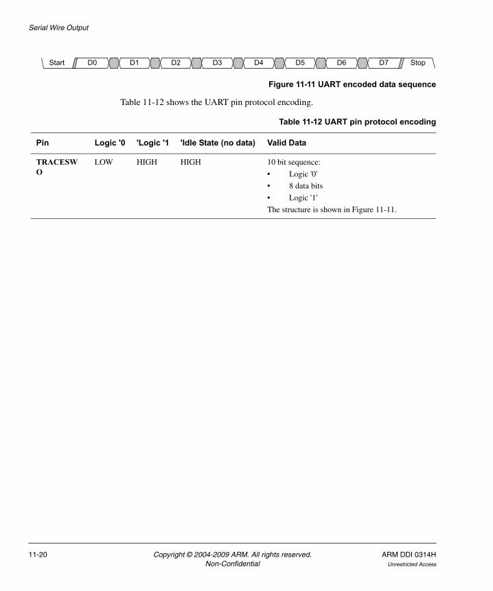
Serial Wire Output
Figure 11-11 UART encoded data sequence
Table 11-12 shows the UART pin protocol encoding.
Start D0 D1 D2 D3 D4 D5 D6 D7 Stop
Table 11-12 UART pin protocol encoding
Pin Logic '0 'Logic '1 'Idle State (no data) Valid Data
TRACESWO
LOW HIGH HIGH 10 bit sequence:
• Logic '0'
• 8 data bits
• Logic '1'
The structure is shown in Figure 11-11.
11-20 Copyright © 2004-2009 ARM. All rights reserved. ARM DDI 0314HNon-Confidential Unrestricted Access
Chapter 12 Instrumentation Trace Macrocell
This chapter describes the Instrumentation Trace Macrocell (ITM). It contains the following sections:
• About the Instrumentation Trace Macrocell on page 12-2
• ITM ports on page 12-9
• ITM programmers model on page 12-10
• CoreSight defined registers on page 12-12
• Stimulus registers on page 12-14
• Trace registers on page 12-16
• Control registers on page 12-18
• Integration test registers on page 12-21
• Authentication requirements on page 12-25.
ARM DDI 0314H Copyright © 2004-2009 ARM. All rights reserved. 12-1Unrestricted Access Non-Confidential
Instrumentation Trace Macrocell
12.1 About the Instrumentation Trace MacrocellThe CoreSight ITM block is a software application driven trace source. Supporting code generates SoftWare Instrumentation Trace (SWIT). In addition, the block provides a coarse-grained timestamp functionality. The main uses for this block are to:
• support printf style debugging
• trace OS and application events
• emit diagnostic system information.
Figure 12-1 shows a block diagram of the ITM.
Figure 12-1 ITM block diagram
The ITM contains the following sub-blocks:
Timestamp Generates timestamp packet.
Sync control ITM synchronizer.
Arbiter Arbitrates between synchronous, timestamp, and SWIT packet.
FIFO ATB First In First Out (FIFO).
Emitter ATB registered emitter.
Data is written to the stimulus registers using the APB interface. See Stimulus registers on page 12-14. This data is then transmitted on the ATB interface as SWIT packets as described in SWIT packet on page 12-7.
The operation of the ITM is described in more detail in:
• ITM ports on page 12-9
• Trace packet format on page 12-3
• Multiple source arbitration on page 12-8
APB interface
CoreSight management
registers
CoreSight ITM-specific registers and integration registers
ATB interface
Sync control
Time stamp
Arbiter FIFO Emitter
APB slave port
ATB master
port
PCLK domain ATCLK domain
12-2 Copyright © 2004-2009 ARM. All rights reserved. ARM DDI 0314HNon-Confidential Unrestricted Access
Instrumentation Trace Macrocell
• ITM FIFO on page 12-8.
12.1.1 Trace packet format
Trace data from ITM is output in packets with a byte protocol. These packets are 1-5 bytes in size, comprising:
• one byte header
• 0-4 byte payload.
Note Synchronization packets differ slightly, and comprise a unique 6-byte sequence for bit and byte synchronization.
Table 12-1 and Table 12-2 show the trace packet encodings.
The ITM trace packets are described in:
• Synchronization packet on page 12-4
• Overflow packet on page 12-4
• Timestamp packet on page 12-5
• SWIT packet on page 12-7
• Reserved encodings on page 12-7.
Table 12-1 Sync packet encoding
Description Packet value Payload Category Notes
Synchronization 0x800000000000 None Synchronization {47{1'b0}} followed by 1'b1. Matches ETM protocol.
Table 12-2 Trace packet encoding
Description Header value Payload Category Notes
Overflow 0b01110000 None Protocol Overflow
Timestamp 0bCDDD0000 0-4 bytes Protocol D = data (!=000) - time
C = continuation
Reserved 0bCxxx0100 0-4 bytes Reserved C = continuation
SWIT 0bBBBBB0SS 1, 2, or 4 bytes Software source (application)
SS = size (!=00) of payload B = SW Source Address
ARM DDI 0314H Copyright © 2004-2009 ARM. All rights reserved. 12-3Unrestricted Access Non-Confidential

Instrumentation Trace Macrocell
Synchronization packet
Synchronization packets are unique patterns in the bit-stream that enable capture hardware to identify bit-to-byte alignment. A synchronization packet is only emitted if the APB interface has been used since the last synchronization packet. Synchronization packets are output by the timestamp packet when the synchronization counter reaches zero. A synchronization packet is forty-seven 1'b0 followed by one 1'b1. Figure 12-2 shows the layout of a synchronization packet.
Figure 12-2 Synchronization packet layout
Overflow packet
Overflow packets can precede all packets except synchronization packets. Overflow is tracked by each source, either SWIT or timestamp.
SWIT overflow is against all stimulus ports. This happens when data is written to the Stimulus Registers but the FIFO is full. Timestamp overflows on reaching the value 2097151.
Figure 12-3 shows the layout of an overflow packet.
Figure 12-3 Overflow packet layout
Note Before disabling the ITM, tools must ensure the FIFO is not full before writing a dummy packet to a Stimulus Register to flush out any overflow information. They must then wait for the ITMBUSY bit to go LOW again, before finally clearing the ITMEn bit.
000001
000000
000000
000000
000000
000000
000000
000000
Byte 0Byte 1Byte 2Byte 3Byte 4Byte 5
MSB LSB
0 1 1 1 0 0 0 0MSB LSB
12-4 Copyright © 2004-2009 ARM. All rights reserved. ARM DDI 0314HNon-Confidential Unrestricted Access
Instrumentation Trace Macrocell
12.1.2 Timestamp packet
Timestamp packets encode timestamp information, generic control, and synchronization. The compression scheme uses delta timestamps. Emitting a timestamp zeroes the time counter. Timestamp resolution is related to the clock on the ATB interface. To prevent overflow, the timestamp is emitted at 95% of the counter limit.
The CoreSight ITM implementation has a 21-bit counter, emitting up to TS[20:0], and emitting a full timestamp at 2,000,000 (21'h1E847F) cycles. The architecture allows for a 28-bit counter.
Figure 12-4 shows the layout of an timestamp packet.
Figure 12-4 Timestamp packet layout
In Figure 12-4:
C Continuation bit, a byte follows.
Leading zeroes are implied where C=0, to compress the timestamp packet into the minimum of bytes.
TS [27:0] Byte packing timestamp information.
TC[2:0] Timestamp control where:
Only one byte output (header only) (C == 0 of Byte 0) Single byte timestamps are optimized encodings for when there is a timestamp of value 1-6 with no skew.
[b000] = Reserved timestamp control.
[b001-b110] = Timestamp emitted synchronous to ITM data.
[b111] = Overflow ITM.
Two+ bytes (header + payload) (C == 1 of Byte 0) [b000-b011] = Reserved timestamp control.
[b100] = Timestamp emitted synchronous to ITM data.
[b101] = Timestamp emitted delayed to ITM.
[b110] = Packet emitted delayed.
[b111] = Packet and timestamp emitted delayed.
CByte 0Byte 1Byte 2Byte 3Byte 4
MSB LSBTC[2] 0 0 0 0
0 TS[27] TS[26] TS[25] TS[24] TS[23] TS[22] TS[21]C TS[20] TS[19] TS[18] TS[17] TS[16] TS[15] TS[14]C TS[13] TS[12] TS[11] TS[10] TS[9] TS[8] TS[7]C TS[6] TS[5] TS[4] TS[3] TS[2] TS[1] TS[0]
TC[1] TC[0]
ARM DDI 0314H Copyright © 2004-2009 ARM. All rights reserved. 12-5Unrestricted Access Non-Confidential

Instrumentation Trace Macrocell
For example, a timestamp value of 7 is transmitted as two bytes. The value of 7 is transmitted in the second byte and delay information in the first byte.
A packet delay marker is emitted when ITM attempts to write to the FIFO but are blocked because of a priority rule, or the FIFO not accepting the data.
A timestamp delay marker is emitted when a timestamp is ready but the FIFO is unable to accept the packet. A delay is not marked if waiting on higher priority transactions, because the timestamp continues to count.
The timestamp counter zeroes on a successful write. Timestamps are appended after the source, SWIT. The exception is if a synchronization packet is transmitted after the SWIT or the timestamp counter has overflowed, so the timestamp is preceded by an OVERFLOW or if a full timestamp reference, two million, is reached and a packet is emitted.
For example, a timestamp is configured to count every ATB clock, with a value of 1001 on the first ITM packet:
1000 idle1001 SWIT1002 fifo not ready1003 fifo not ready1004 TS=1004 with TS delay marked (3 Bytes 0xd0, 0xec, 0x07)0 SWIT1 SWIT2 TS=2 (single byte 0x20)0 SWIT1 fifo not ready / ITM packet presented but not accepted2 SWIT3 TS=3 packet delay marked (2 Bytes 0xe0, 0x03)0 idle1 idle2 idle...1999997 idle1999998 idle1999999 TS=1999999 (2,000,000 ticks)0 idle1 idle...2097146 fifo not ready2097147 fifo not ready / ITM packet presented but not accepted2097148 SWIT packet2097149 fifo not ready2097150 fifo not ready2097151 fifo not ready (2^21 limit)0 fifo not ready
12-6 Copyright © 2004-2009 ARM. All rights reserved. ARM DDI 0314HNon-Confidential Unrestricted Access
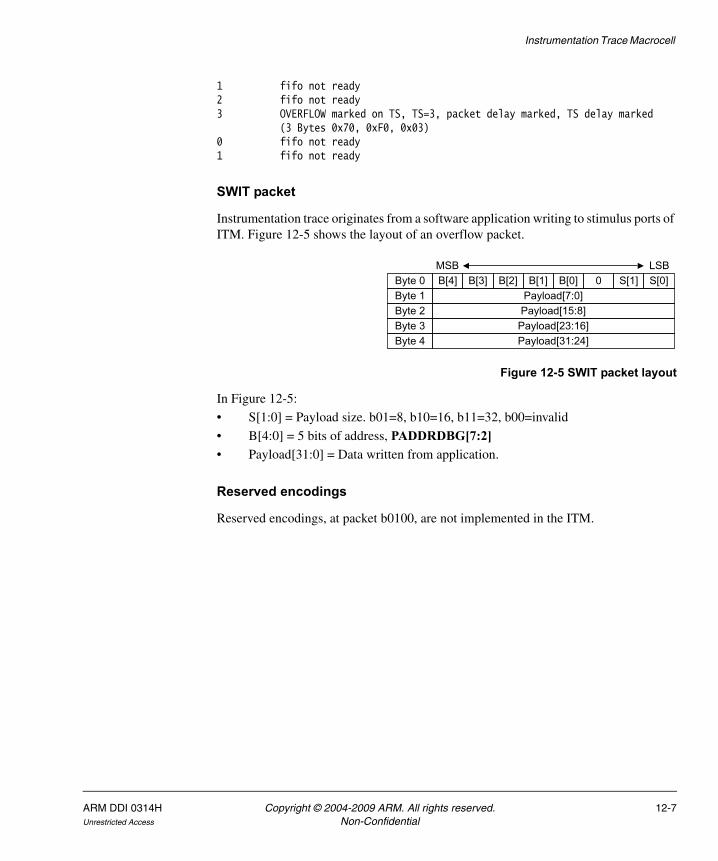
Instrumentation Trace Macrocell
1 fifo not ready2 fifo not ready3 OVERFLOW marked on TS, TS=3, packet delay marked, TS delay marked
(3 Bytes 0x70, 0xF0, 0x03)0 fifo not ready1 fifo not ready
SWIT packet
Instrumentation trace originates from a software application writing to stimulus ports of ITM. Figure 12-5 shows the layout of an overflow packet.
Figure 12-5 SWIT packet layout
In Figure 12-5:
• S[1:0] = Payload size. b01=8, b10=16, b11=32, b00=invalid
• B[4:0] = 5 bits of address, PADDRDBG[7:2]• Payload[31:0] = Data written from application.
Reserved encodings
Reserved encodings, at packet b0100, are not implemented in the ITM.
B[4]Payload[7:0]
B[3] B[2] B[1] B[0] 0 S[1] S[0]Byte 0Byte 1Byte 2Byte 3Byte 4
MSB LSB
Payload[15:8]Payload[23:16]Payload[31:24]
ARM DDI 0314H Copyright © 2004-2009 ARM. All rights reserved. 12-7Unrestricted Access Non-Confidential
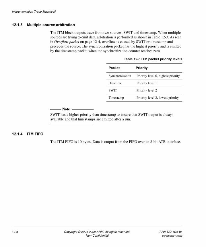
Instrumentation Trace Macrocell
12.1.3 Multiple source arbitration
The ITM block outputs trace from two sources, SWIT and timestamp. When multiple sources are trying to emit data, arbitration is performed as shown in Table 12-3. As seen in Overflow packet on page 12-4, overflow is caused by SWIT or timestamp and precedes the source. The synchronization packet has the highest priority and is emitted by the timestamp packet when the synchronization counter reaches zero.
Note SWIT has a higher priority than timestamp to ensure that SWIT output is always available and that timestamps are emitted after a run.
12.1.4 ITM FIFO
The ITM FIFO is 10 bytes. Data is output from the FIFO over an 8-bit ATB interface.
Table 12-3 ITM packet priority levels
Packet Priority
Synchronization Priority level 0, highest priority
Overflow Priority level 1
SWIT Priority level 2
Timestamp Priority level 3, lowest priority
12-8 Copyright © 2004-2009 ARM. All rights reserved. ARM DDI 0314HNon-Confidential Unrestricted Access

Instrumentation Trace Macrocell
12.2 ITM portsThe ITM ports are described in:
• Clocks and resets
• APB interface
• ATB interface
• Miscellaneous ports.
12.2.1 Clocks and resets
The ITM has two clock domains. One is for the APB interface, PCLKDBG, the other is for the ATB interface, ATCLK.
12.2.2 APB interface
The ITM has an AMBA 3 APB interface that restricts accesses to pure 32-bit transfers. This interface is used both to stimulate trace and to control the ITM. To reduce the data overhead when only writing low values to stimulus registers, the ITM uses leading zero compression on data values.
Stalled transfers are not permitted to registers between 0x000 and 0xDFC. This ensures that any writes to present or future stimulus registers do not decrease system performance.
12.2.3 ATB interface
ATB trace data is 8 bits wide and, therefore, the ATBYTES signal is not required. The flush control, AFVALIDM, is not implemented in the ITM. The ITM indicates when the FIFO is empty by asserting AFREADYM HIGH.
12.2.4 Miscellaneous ports
Table 12-4 shows the miscellaneous ITM ports.
Table 12-4 Miscellaneous ports
Name Type Description
TRIGOUT Output Indicates a trigger event, that is, a write to a stimulus register that has a trigger enable against it
TRIGOUTACK Input Asynchronous TRIGOUT acknowledgement signal
ARM DDI 0314H Copyright © 2004-2009 ARM. All rights reserved. 12-9Unrestricted Access Non-Confidential
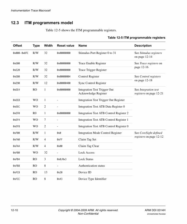
Instrumentation Trace Macrocell
12.3 ITM programmers modelTable 12-5 shows the ITM programmable registers.
Table 12-5 ITM programmable registers
Offset Type Width Reset value Name Description
0x000- 0x07C R/W 32 0x00000000 Stimulus Port Register 0 to 31 See Stimulus registers on page 12-14
0xE00 R/W 32 0x00000000 Trace Enable Register See Trace registers on page 12-16
0xE20 R/W 32 0x00000000 Trace Trigger Register
0xE80 R/W 32 0x00000004 Control Register See Control registers on page 12-18
0xE90 R/W 12 0x00000400 Sync Control Register
0xEE4 RO 1 0x00000000 Integration Test Trigger Out Acknowledge Register
See Integration test registers on page 12-21
0xEE8 WO 1 - Integration Test Trigger Out Register
0xEEC WO 2 - Integration Test ATB Data Register 0
0xEF0 R0 1 0x00000000 Integration Test ATB Control Register 2
0xEF4 WO 7 - Integration Test ATB Control Register 1
0xEF8 WO 2 - Integration Test ATB Control Register 0
0xF00 R/W 1 0x0 Integration Mode Control Register See CoreSight defined registers on page 12-12
0xFA0 R/W 4 0xFF Claim Tag Set
0xFA4 R/W 4 0x00 Claim Tag Clear
0xFB0 WO 32 - Lock Access
0xFB4 RO 3 0x0/0x3 Lock Status
0xFB8 RO 8 - Authentication status
0xFC8 RO 13 0x20 Device ID
0xFCC RO 8 0x43 Device Type Identifier
12-10 Copyright © 2004-2009 ARM. All rights reserved. ARM DDI 0314HNon-Confidential Unrestricted Access
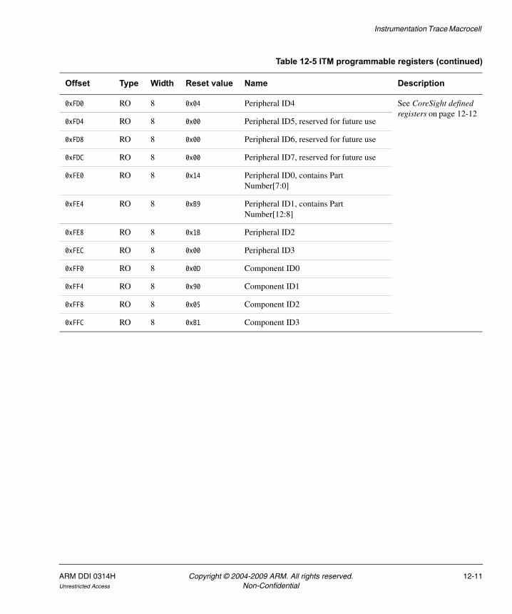
Instrumentation Trace Macrocell
0xFD0 RO 8 0x04 Peripheral ID4 See CoreSight defined registers on page 12-12
0xFD4 RO 8 0x00 Peripheral ID5, reserved for future use
0xFD8 RO 8 0x00 Peripheral ID6, reserved for future use
0xFDC RO 8 0x00 Peripheral ID7, reserved for future use
0xFE0 RO 8 0x14 Peripheral ID0, contains Part Number[7:0]
0xFE4 RO 8 0xB9 Peripheral ID1, contains Part Number[12:8]
0xFE8 RO 8 0x1B Peripheral ID2
0xFEC RO 8 0x00 Peripheral ID3
0xFF0 RO 8 0x0D Component ID0
0xFF4 RO 8 0x90 Component ID1
0xFF8 RO 8 0x05 Component ID2
0xFFC RO 8 0xB1 Component ID3
Table 12-5 ITM programmable registers (continued)
Offset Type Width Reset value Name Description
ARM DDI 0314H Copyright © 2004-2009 ARM. All rights reserved. 12-11Unrestricted Access Non-Confidential
Instrumentation Trace Macrocell
12.4 CoreSight defined registersThese registers are described in the CoreSight Architecture Specification. This section describes the values that are specific to the ITM.
12.4.1 Integration Mode Control Register, 0xF00
This register enables the component to switch from a functional mode, the default behavior, to integration mode. The ITM must be disabled and be in the idle state before setting the Integration Mode.
12.4.2 Claim Tag Set Register, 0xFA0, and Claim Tag Clear Register, 0xFA4
The ITM implements an 8-bit claim tag.
12.4.3 Lock Access Register, 0xFB0, and Lock Status Register, 0xFB4
When PADDRDBG31 is LOW, the Lock Status Register reads as 0x3 from the reset indicating that a 32-bit Lock Access Register is present. The lock access mechanism is not present for any access to stimulus registers (offsets 0x000 to 0x07C) and is also not present when PADDRDBG31 is HIGH.
12.4.4 Authentication Status Register, 0xFB8
Authentication Status Register == 8'b1S001N00 where S is secure non-invasive debug state and N is non-secure, non-invasive debug.
12.4.5 Device Configuration Register, 0xFC8
This register specifies the number of stimulus registers implemented, and reads as 0x20 indicating that 32 stimulus are available.
12.4.6 Device Type Identifier Register, 0xFCC
This register reads as 0x43 indicating that the device is a Trace Source (0x3) and the stimulus is derived from bus activity (0x4)
12.4.7 Peripheral ID Registers, 0xFDC-0xFE0
The ITM has the designer identity of ARM (0x38) with continuation code 0x4 and a part number of 0x913. This device uses only 4KB of memory.
12-12 Copyright © 2004-2009 ARM. All rights reserved. ARM DDI 0314HNon-Confidential Unrestricted Access
Instrumentation Trace Macrocell
12.4.8 Component ID Registers (0xFFC to 0xFF0)
The component class reads as 0x9 indicating that the ITM is a CoreSight component.
ARM DDI 0314H Copyright © 2004-2009 ARM. All rights reserved. 12-13Unrestricted Access Non-Confidential
Instrumentation Trace Macrocell
12.5 Stimulus registersEach of the 32 stimulus ports is represented by a virtual address, creating 32 stimulus registers. A write to one of these locations causes data to be written into the FIFO if the corresponding bit in the Trace Enable Register is set and ITM is enabled. Reading from any of the stimulus ports returns the FIFO status (notFull(1) / Full(0)) only if the ITM is enabled. This enables more efficient core register allocation because the stimulus address has already been generated.
The ITM transmits SWIT packets using leading zero compression. Packets can be 8, 16, or 32 bits. See SWIT packet on page 12-7.
The bank of 32 registers is split into a low-16 (0 to 15) and a high-16 (16 to 31). Writes to the high-16 are discarded by the ITM whenever secure non-invasive trace is disabled, regardless of how the Trace Enable Register bits [31:16] are set. Both the high-16 and low-16 are be disabled when non-invasive trace is disabled. When an input is disabled it must not alter the interface response and must always return an OK without stalling.
Note Any instrumented secure code must use the upper 16 (16-31) register locations that are masked against secure non-invasive enable. You must enable both secure and non-secure transactions to the ITM.
The APB interface does not provide an atomic Read Modify Write (RMW), so an exclusive monitor must be used if a polled printf is used concurrently with ITM usage by interrupts or other threads. The following polled code guarantees stimulus is not lost by polled access to the ITM:
; R0 = FIFO-full/exclusive status; R1 = base of ITM stimulus ports; R2 = value to write
retryLDREX R0,[R1,#??] ; read FIFO status and request excl lockCZBEQ R0,retry ; FIFO not ready, try againSTREX R0,R2,[R1,#??] ; store if FIFO !Full and excl lockCZBNE R0,retry ; excl lock failed, try again
If multiple writes are performed to the ITM when the FIFO is full, the transaction is discarded although no error or stall is generated on the interface.
These registers are not blocked by the Lock Access Register.
Writes to registers to 0x080-0xDFC result in no SWIT packet being transmitted. Reads from these registers return a 0x0. This address space is reserved for future stimulus registers.
12-14 Copyright © 2004-2009 ARM. All rights reserved. ARM DDI 0314HNon-Confidential Unrestricted Access
Instrumentation Trace Macrocell
Note The DEVID specifies how many stimulus registers are implemented.
ARM DDI 0314H Copyright © 2004-2009 ARM. All rights reserved. 12-15Unrestricted Access Non-Confidential
Instrumentation Trace Macrocell
12.6 Trace registersThis section describes the trace registers:
• Trace Enable Register, TER, 0xE00
• Trace Trigger Register, TTR, 0xE20.
12.6.1 Trace Enable Register, TER, 0xE00
Each bit location corresponds to a virtual stimulus register; when a bit is set, a write to the appropriate stimulus location results in a packet being generated, except when the FIFO is full. Reset to disable all locations is 0x00000000.
The setting of the bits [31:16] is ignored if secure trace is disabled. Stimulus ports 16-31 are disabled when the ability to perform secure non-invasive debug is removed.
The setting of the bits [31:0] is ignored if non-secure trace is disabled. Stimulus ports 0-31 are disabled when the ability to perform non-secure non-invasive debug is removed.
Table 12-6 shows the Trace Enable Register bit assignments.
12.6.2 Trace Trigger Register, TTR, 0xE20
Each bit in the register represents one of the virtual stimulus registers. When the bit is set, a pulse is sent on TRIGOUT when writing to the corresponding Stimulus Register. The pulse is held until TRIGOUTACK is returned, which can result in masking of multiple triggers with one acknowledgement. Triggers are not generated if trace is disabled. When secure non-invasive debug, or secure trace, is disabled, no triggers are generated for Stimulus Registers 16 to 31. If non-secure non-invasive debug, or trace, is disabled, no triggers are generated. The register is zero on reset, and the default is no triggers generated.
Table 12-7 shows the Trace Trigger Register bit assignments.
Table 12-6 Trace Enable Register bit assignments
Bits Name Description
[31:0] Trace Enable Register Bit mask to enable tracing on ITM stimulus ports.
Table 12-7 Trace Trigger Register bit assignments
Bits Name Description
[31:0] Trigger Mask Bit mask to enable trigger generation, TRIGOUT, on selected writes to the Stimulus Registers
12-16 Copyright © 2004-2009 ARM. All rights reserved. ARM DDI 0314HNon-Confidential Unrestricted Access
Instrumentation Trace Macrocell
Figure 12-6 shows two writes to the stimulus port. It shows the timing for generating TRIGOUT and deasserting TRIGOUT with TRIGOUTACK. PENABLE and PREADY show when a write happens to the Stimulus Register.
Figure 12-6 TRIGOUT and TRIGOUTACK operation
The write at T0-T2 causes the TRIGOUT. This is acknowledged at T5. A write at T2-T4 generates another TRIGOUT. If the TRIGOUTACK stays HIGH beyond T6, this TRIGOUT is also acknowledged at T6. In the example TRIGOUTACK goes LOW before T6, so another TRIGOUTACK is required.
ATCLK PCLKDBG
T0 T1 T2 T3 T4 T5 T6 T7 T8
TRIGOUT
TRIGOUTACK
PENABLE
PREADY
PWRITE
ARM DDI 0314H Copyright © 2004-2009 ARM. All rights reserved. 12-17Unrestricted Access Non-Confidential
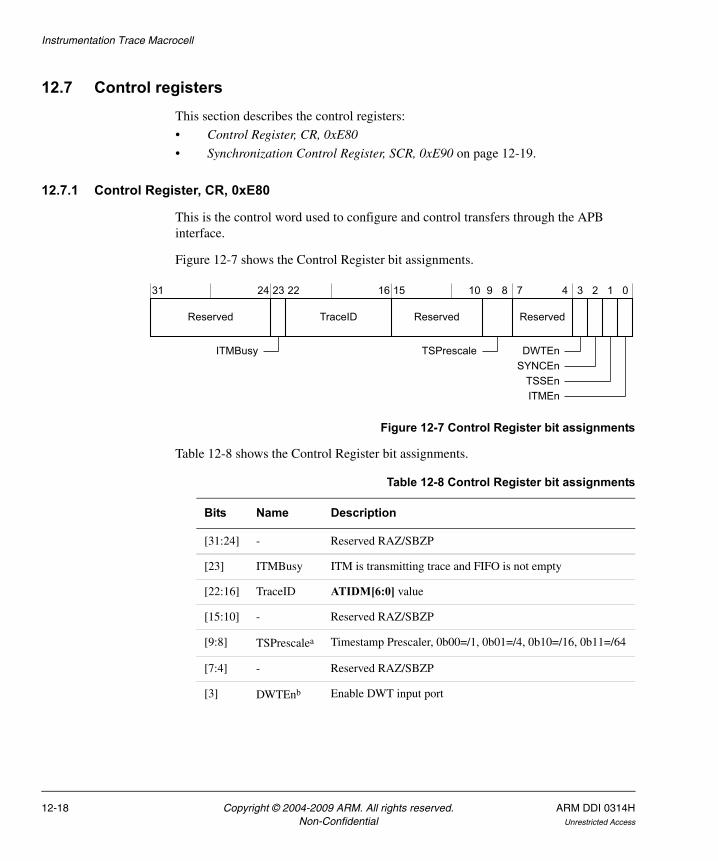
Instrumentation Trace Macrocell
12.7 Control registersThis section describes the control registers:
• Control Register, CR, 0xE80
• Synchronization Control Register, SCR, 0xE90 on page 12-19.
12.7.1 Control Register, CR, 0xE80
This is the control word used to configure and control transfers through the APB interface.
Figure 12-7 shows the Control Register bit assignments.
Figure 12-7 Control Register bit assignments
Table 12-8 shows the Control Register bit assignments.
Reserved
31 24 23 22 16 15 10 9 8 7 4 3 2 1 0
TraceID Reserved Reserved
ITMBusy TSPrescale DWTEnSYNCEn
TSSEnITMEn
Table 12-8 Control Register bit assignments
Bits Name Description
[31:24] - Reserved RAZ/SBZP
[23] ITMBusy ITM is transmitting trace and FIFO is not empty
[22:16] TraceID ATIDM[6:0] value
[15:10] - Reserved RAZ/SBZP
[9:8] TSPrescalea Timestamp Prescaler, 0b00=/1, 0b01=/4, 0b10=/16, 0b11=/64
[7:4] - Reserved RAZ/SBZP
[3] DWTEnb Enable DWT input port
12-18 Copyright © 2004-2009 ARM. All rights reserved. ARM DDI 0314HNon-Confidential Unrestricted Access

Instrumentation Trace Macrocell
12.7.2 Synchronization Control Register, SCR, 0xE90
Synchronization packets must be output on a regular basis to provide decompression tools markers in the trace stream. The first synchronization packet is output when the ITM is enabled by setting bit [0] in the Control Register. Subsequent packets are output when the counter reaches zero, that is, decrement on data entered into the FIFO. The Synchronization Control Register represents the reloaded count value when the counter reaches zero, not the current count. This register must only be changed when the ITM is disabled.
Note A value of 0x000 written to the Synchronization Control Register causes unpredictable results. This value must only be used when a synchronization counter is not implemented. This register always reads as zero if no synchronization counter is implemented. A counter can be detected by attempting to write a non-zero value to the register and reading it back. The default value is 0x400.
Figure 12-8 shows the Synchronization Control Register bit assignments.
Figure 12-8 Synchronization Control Register bit assignments
[2] SYNCEnc Enable sync packets
[1] TSSEn Enable timestamps, delta
[0] ITMEnd Enable ITM stimulus, also acts as a global enable
a. The TSPrescale bit is reset to 0x0. This means that the timestamp counts on every ATCLK tick. However, you can program the TSPrescale bit so that the timestamp counts once every 4, 16, or 64 ATCLK ticks.
b. Data Watchpoint and Trace (DWT) is not used in the CoreSight ITM, so the DWTEn bit is always 0x0.
c. The SYNCEn bit is always 0x1 and is enabled.d. It is recommended that the ITMEn bit is cleared and waits for the ITMBusy bit to be
cleared, before changing any fields in the Control Register, otherwise the behavior can be unpredictable. See Overflow packet on page 12-4 for information about disabling the ITM overflow packets.
Table 12-8 Control Register bit assignments (continued)
Bits Name Description
Reserved
31 12 11 0
Sync Count
ARM DDI 0314H Copyright © 2004-2009 ARM. All rights reserved. 12-19Unrestricted Access Non-Confidential

Instrumentation Trace Macrocell
Table 12-9 shows the Synchronization Control Register bit assignments.
Table 12-9 Synchronization Control Register bit assignments
Bits Name Description
[31:12] - Reserved RAZ/SBZP
[11:0] Sync Count Counter value for time between synchronization markers
12-20 Copyright © 2004-2009 ARM. All rights reserved. ARM DDI 0314HNon-Confidential Unrestricted Access
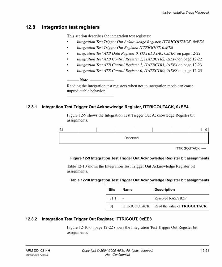
Instrumentation Trace Macrocell
12.8 Integration test registersThis section describes the integration test registers:
• Integration Test Trigger Out Acknowledge Register, ITTRIGOUTACK, 0xEE4
• Integration Test Trigger Out Register, ITTRIGOUT, 0xEE8
• Integration Test ATB Data Register 0, ITATBDATA0, 0xEEC on page 12-22
• Integration Test ATB Control Register 2, ITATBCTR2, 0xEF0 on page 12-22
• Integration Test ATB Control Register 1, ITATBCTR1, 0xEF4 on page 12-23
• Integration Test ATB Control Register 0, ITATBCTR0, 0xEF8 on page 12-23
Note Reading the integration test registers when not in integration mode can cause unpredictable behavior.
12.8.1 Integration Test Trigger Out Acknowledge Register, ITTRIGOUTACK, 0xEE4
Figure 12-9 shows the Integration Test Trigger Out Acknowledge Register bit assignments.
Figure 12-9 Integration Test Trigger Out Acknowledge Register bit assignments
Table 12-10 shows the Integration Test Trigger Out Acknowledge Register bit assignments.
12.8.2 Integration Test Trigger Out Register, ITTRIGOUT, 0xEE8
Figure 12-10 on page 12-22 shows the Integration Test Trigger Out Register bit assignments.
Reserved
31 1 0
ITTRIGOUTACK
Table 12-10 Integration Test Trigger Out Acknowledge Register bit assignments
Bits Name Description
[31:1] - Reserved RAZ/SBZP
[0] ITTRIGOUTACK Read the value of TRIGOUTACK
ARM DDI 0314H Copyright © 2004-2009 ARM. All rights reserved. 12-21Unrestricted Access Non-Confidential
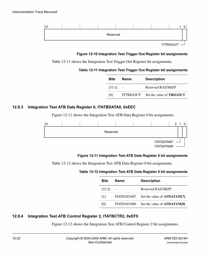
Instrumentation Trace Macrocell
Figure 12-10 Integration Test Trigger Out Register bit assignments
Table 12-11 shows the Integration Test Trigger Out Register bit assignments.
12.8.3 Integration Test ATB Data Register 0, ITATBDATA0, 0xEEC
Figure 12-11 shows the Integration Test ATB Data Register 0 bit assignments.
Figure 12-11 Integration Test ATB Data Register 0 bit assignments
Table 12-12 shows the Integration Test ATB Data Register 0 bit assignments.
12.8.4 Integration Test ATB Control Register 2, ITATBCTR2, 0xEF0
Figure 12-12 shows the Integration Test ATB Control Register 2 bit assignments.
Reserved
31 1 0
ITTRIGOUT
Table 12-11 Integration Test Trigger Out Register bit assignments
Bits Name Description
[31:1] - Reserved RAZ/SBZP
[0] ITTRIGOUT Set the value of TRIGOUT
Reserved
31 2 1 0
ITATDATAM7ITATDATAM0
Table 12-12 Integration Test ATB Data Register 0 bit assignments
Bits Name Description
[31:2] - Reserved RAZ/SBZP
[1] ITATDATAM7 Set the value of ATDATAM[7]
[0] ITATDATAM0 Set the value of ATDATAM[0]
12-22 Copyright © 2004-2009 ARM. All rights reserved. ARM DDI 0314HNon-Confidential Unrestricted Access
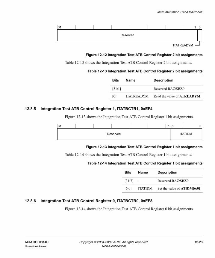
Instrumentation Trace Macrocell
Figure 12-12 Integration Test ATB Control Register 2 bit assignments
Table 12-13 shows the Integration Test ATB Control Register 2 bit assignments.
12.8.5 Integration Test ATB Control Register 1, ITATBCTR1, 0xEF4
Figure 12-13 shows the Integration Test ATB Control Register 1 bit assignments.
Figure 12-13 Integration Test ATB Control Register 1 bit assignments
Table 12-14 shows the Integration Test ATB Control Register 1 bit assignments.
12.8.6 Integration Test ATB Control Register 0, ITATBCTR0, 0xEF8
Figure 12-14 shows the Integration Test ATB Control Register 0 bit assignments.
Reserved
31 1 0
ITATREADYM
Table 12-13 Integration Test ATB Control Register 2 bit assignments
Bits Name Description
[31:1] - Reserved RAZ/SBZP
[0] ITATREADYM Read the value of ATREADYM
Reserved
31 0
ITATIDM
7 6
Table 12-14 Integration Test ATB Control Register 1 bit assignments
Bits Name Description
[31:7] - Reserved RAZ/SBZP
[6:0] ITATIDM Set the value of ATIDM[6:0]
ARM DDI 0314H Copyright © 2004-2009 ARM. All rights reserved. 12-23Unrestricted Access Non-Confidential
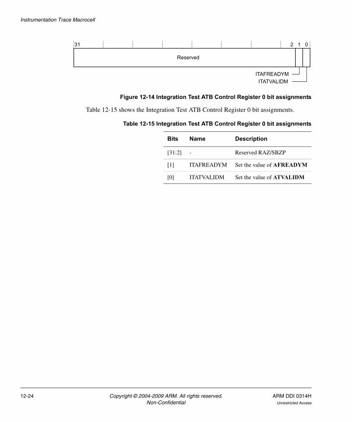
Instrumentation Trace Macrocell
Figure 12-14 Integration Test ATB Control Register 0 bit assignments
Table 12-15 shows the Integration Test ATB Control Register 0 bit assignments.
Reserved
31 1 0
ITATVALIDM
2
ITAFREADYM
Table 12-15 Integration Test ATB Control Register 0 bit assignments
Bits Name Description
[31:2] - Reserved RAZ/SBZP
[1] ITAFREADYM Set the value of AFREADYM
[0] ITATVALIDM Set the value of ATVALIDM
12-24 Copyright © 2004-2009 ARM. All rights reserved. ARM DDI 0314HNon-Confidential Unrestricted Access
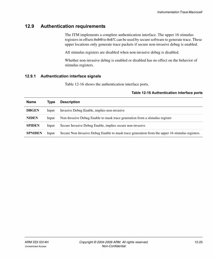
Instrumentation Trace Macrocell
12.9 Authentication requirementsThe ITM implements a complete authentication interface. The upper 16 stimulus registers in offsets 0x040 to 0x07C can be used by secure software to generate trace. These upper locations only generate trace packets if secure non-invasive debug is enabled.
All stimulus registers are disabled when non-invasive debug is disabled.
Whether non-invasive debug is enabled or disabled has no effect on the behavior of stimulus registers.
12.9.1 Authentication interface signals
Table 12-16 shows the authentication interface ports.
Table 12-16 Authentication interface ports
Name Type Description
DBGEN Input Invasive Debug Enable, implies non-invasive
NIDEN Input Non-Invasive Debug Enable to mask trace generation from a stimulus register
SPIDEN Input Secure Invasive Debug Enable, implies secure non-invasive
SPNIDEN Input Secure Non-Invasive Debug Enable to mask trace generation from the upper 16 stimulus registers.
ARM DDI 0314H Copyright © 2004-2009 ARM. All rights reserved. 12-25Unrestricted Access Non-Confidential

Instrumentation Trace Macrocell
12-26 Copyright © 2004-2009 ARM. All rights reserved. ARM DDI 0314HNon-Confidential Unrestricted Access
Appendix A CoreSight Port List
This appendix describes the CoreSight port and interface signals. It contains the following sections:
• Clock domains on page A-2
• CoreSight DAP signals on page A-3
• CoreSight ECT signals on page A-9
• CoreSight replicator signals on page A-12
• CoreSight synchronous bridge signals on page A-14
• CoreSight trace funnel signals on page A-15
• CoreSight TPIU signals on page A-19
• CoreSight ETB signals on page A-21
• CoreSight SWO signals on page A-23
• CoreSight ITM signals on page A-24.
ARM DDI 0314H Copyright © 2004-2009 ARM. All rights reserved. A-1Unrestricted Access Non-Confidential
CoreSight Port List
A.1 Clock domainsIn addition to the names of clock domains there are the following entries in the port lists:
• N/A, not applicable. This is used for the clock signals.
• None. This signal is an asynchronous input. This input can be from any clock domain because the block has internal synchronizers for this signal.
• xx/None. This signal can be from clock domain 'xx' or it can be asynchronous. The signal has bypassable synchronizers. It depends on which configuration the designer chooses.
A-2 Copyright © 2004-2009 ARM. All rights reserved. ARM DDI 0314HNon-Confidential Unrestricted Access
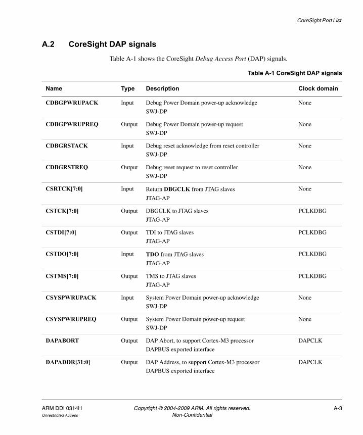
CoreSight Port List
A.2 CoreSight DAP signalsTable A-1 shows the CoreSight Debug Access Port (DAP) signals.
Table A-1 CoreSight DAP signals
Name Type Description Clock domain
CDBGPWRUPACK Input Debug Power Domain power-up acknowledge
SWJ-DP
None
CDBGPWRUPREQ Output Debug Power Domain power-up request
SWJ-DP
None
CDBGRSTACK Input Debug reset acknowledge from reset controller
SWJ-DP
None
CDBGRSTREQ Output Debug reset request to reset controller
SWJ-DP
None
CSRTCK[7:0] Input Return DBGCLK from JTAG slaves
JTAG-AP
None
CSTCK[7:0] Output DBGCLK to JTAG slaves
JTAG-AP
PCLKDBG
CSTDI[7:0] Output TDI to JTAG slaves
JTAG-AP
PCLKDBG
CSTDO[7:0] Input TDO from JTAG slaves
JTAG-AP
PCLKDBG
CSTMS[7:0] Output TMS to JTAG slaves
JTAG-AP
PCLKDBG
CSYSPWRUPACK Input System Power Domain power-up acknowledge
SWJ-DP
None
CSYSPWRUPREQ Output System Power Domain power-up request
SWJ-DP
None
DAPABORT Output DAP Abort, to support Cortex-M3 processor
DAPBUS exported interface
DAPCLK
DAPADDR[31:0] Output DAP Address, to support Cortex-M3 processor
DAPBUS exported interface
DAPCLK
ARM DDI 0314H Copyright © 2004-2009 ARM. All rights reserved. A-3Unrestricted Access Non-Confidential
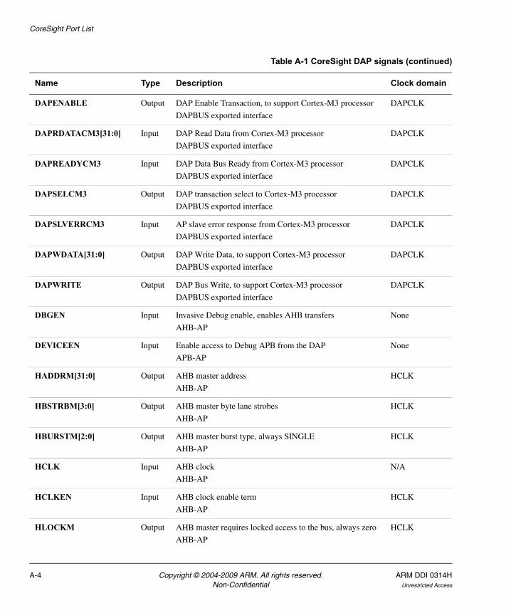
CoreSight Port List
DAPENABLE Output DAP Enable Transaction, to support Cortex-M3 processor
DAPBUS exported interface
DAPCLK
DAPRDATACM3[31:0] Input DAP Read Data from Cortex-M3 processor
DAPBUS exported interface
DAPCLK
DAPREADYCM3 Input DAP Data Bus Ready from Cortex-M3 processor
DAPBUS exported interface
DAPCLK
DAPSELCM3 Output DAP transaction select to Cortex-M3 processor
DAPBUS exported interface
DAPCLK
DAPSLVERRCM3 Input AP slave error response from Cortex-M3 processor
DAPBUS exported interface
DAPCLK
DAPWDATA[31:0] Output DAP Write Data, to support Cortex-M3 processor
DAPBUS exported interface
DAPCLK
DAPWRITE Output DAP Bus Write, to support Cortex-M3 processor
DAPBUS exported interface
DAPCLK
DBGEN Input Invasive Debug enable, enables AHB transfers
AHB-AP
None
DEVICEEN Input Enable access to Debug APB from the DAP
APB-AP
None
HADDRM[31:0] Output AHB master address
AHB-AP
HCLK
HBSTRBM[3:0] Output AHB master byte lane strobes
AHB-AP
HCLK
HBURSTM[2:0] Output AHB master burst type, always SINGLE
AHB-AP
HCLK
HCLK Input AHB clock
AHB-AP
N/A
HCLKEN Input AHB clock enable term
AHB-AP
HCLK
HLOCKM Output AHB master requires locked access to the bus, always zero
AHB-AP
HCLK
Table A-1 CoreSight DAP signals (continued)
Name Type Description Clock domain
A-4 Copyright © 2004-2009 ARM. All rights reserved. ARM DDI 0314HNon-Confidential Unrestricted Access
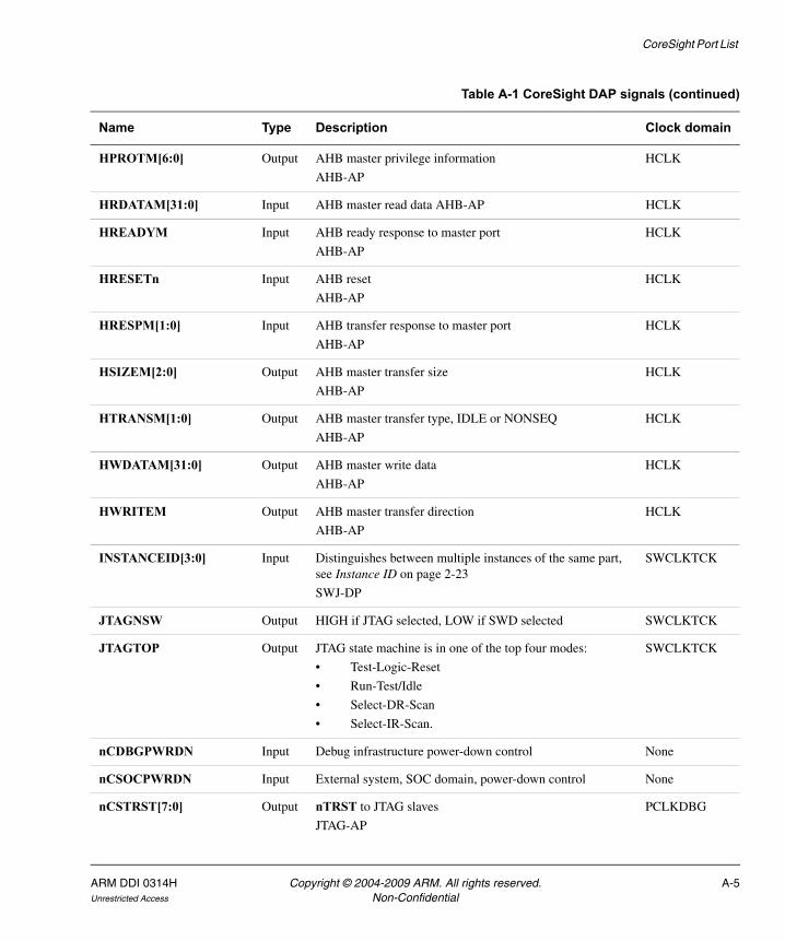
CoreSight Port List
HPROTM[6:0] Output AHB master privilege information
AHB-AP
HCLK
HRDATAM[31:0] Input AHB master read data AHB-AP HCLK
HREADYM Input AHB ready response to master port
AHB-AP
HCLK
HRESETn Input AHB reset
AHB-AP
HCLK
HRESPM[1:0] Input AHB transfer response to master port
AHB-AP
HCLK
HSIZEM[2:0] Output AHB master transfer size
AHB-AP
HCLK
HTRANSM[1:0] Output AHB master transfer type, IDLE or NONSEQ
AHB-AP
HCLK
HWDATAM[31:0] Output AHB master write data
AHB-AP
HCLK
HWRITEM Output AHB master transfer direction
AHB-AP
HCLK
INSTANCEID[3:0] Input Distinguishes between multiple instances of the same part, see Instance ID on page 2-23
SWJ-DP
SWCLKTCK
JTAGNSW Output HIGH if JTAG selected, LOW if SWD selected SWCLKTCK
JTAGTOP Output JTAG state machine is in one of the top four modes:
• Test-Logic-Reset
• Run-Test/Idle
• Select-DR-Scan
• Select-IR-Scan.
SWCLKTCK
nCDBGPWRDN Input Debug infrastructure power-down control None
nCSOCPWRDN Input External system, SOC domain, power-down control None
nCSTRST[7:0] Output nTRST to JTAG slaves
JTAG-AP
PCLKDBG
Table A-1 CoreSight DAP signals (continued)
Name Type Description Clock domain
ARM DDI 0314H Copyright © 2004-2009 ARM. All rights reserved. A-5Unrestricted Access Non-Confidential
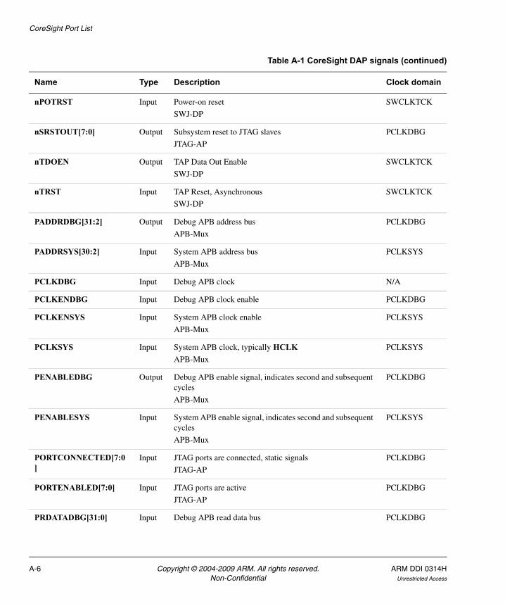
CoreSight Port List
nPOTRST Input Power-on reset
SWJ-DP
SWCLKTCK
nSRSTOUT[7:0] Output Subsystem reset to JTAG slaves
JTAG-AP
PCLKDBG
nTDOEN Output TAP Data Out Enable
SWJ-DP
SWCLKTCK
nTRST Input TAP Reset, Asynchronous
SWJ-DP
SWCLKTCK
PADDRDBG[31:2] Output Debug APB address bus
APB-Mux
PCLKDBG
PADDRSYS[30:2] Input System APB address bus
APB-Mux
PCLKSYS
PCLKDBG Input Debug APB clock N/A
PCLKENDBG Input Debug APB clock enable PCLKDBG
PCLKENSYS Input System APB clock enable
APB-Mux
PCLKSYS
PCLKSYS Input System APB clock, typically HCLKAPB-Mux
PCLKSYS
PENABLEDBG Output Debug APB enable signal, indicates second and subsequent cycles
APB-Mux
PCLKDBG
PENABLESYS Input System APB enable signal, indicates second and subsequent cycles
APB-Mux
PCLKSYS
PORTCONNECTED[7:0]
Input JTAG ports are connected, static signals
JTAG-AP
PCLKDBG
PORTENABLED[7:0] Input JTAG ports are active
JTAG-AP
PCLKDBG
PRDATADBG[31:0] Input Debug APB read data bus PCLKDBG
Table A-1 CoreSight DAP signals (continued)
Name Type Description Clock domain
A-6 Copyright © 2004-2009 ARM. All rights reserved. ARM DDI 0314HNon-Confidential Unrestricted Access
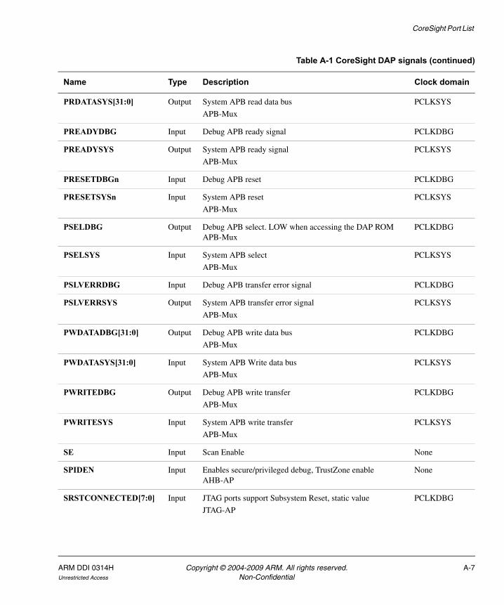
CoreSight Port List
PRDATASYS[31:0] Output System APB read data bus
APB-Mux
PCLKSYS
PREADYDBG Input Debug APB ready signal PCLKDBG
PREADYSYS Output System APB ready signal
APB-Mux
PCLKSYS
PRESETDBGn Input Debug APB reset PCLKDBG
PRESETSYSn Input System APB reset
APB-Mux
PCLKSYS
PSELDBG Output Debug APB select. LOW when accessing the DAP ROM APB-Mux
PCLKDBG
PSELSYS Input System APB select
APB-Mux
PCLKSYS
PSLVERRDBG Input Debug APB transfer error signal PCLKDBG
PSLVERRSYS Output System APB transfer error signal
APB-Mux
PCLKSYS
PWDATADBG[31:0] Output Debug APB write data bus
APB-Mux
PCLKDBG
PWDATASYS[31:0] Input System APB Write data bus
APB-Mux
PCLKSYS
PWRITEDBG Output Debug APB write transfer
APB-Mux
PCLKDBG
PWRITESYS Input System APB write transfer
APB-Mux
PCLKSYS
SE Input Scan Enable None
SPIDEN Input Enables secure/privileged debug, TrustZone enable AHB-AP
None
SRSTCONNECTED[7:0] Input JTAG ports support Subsystem Reset, static value
JTAG-AP
PCLKDBG
Table A-1 CoreSight DAP signals (continued)
Name Type Description Clock domain
ARM DDI 0314H Copyright © 2004-2009 ARM. All rights reserved. A-7Unrestricted Access Non-Confidential
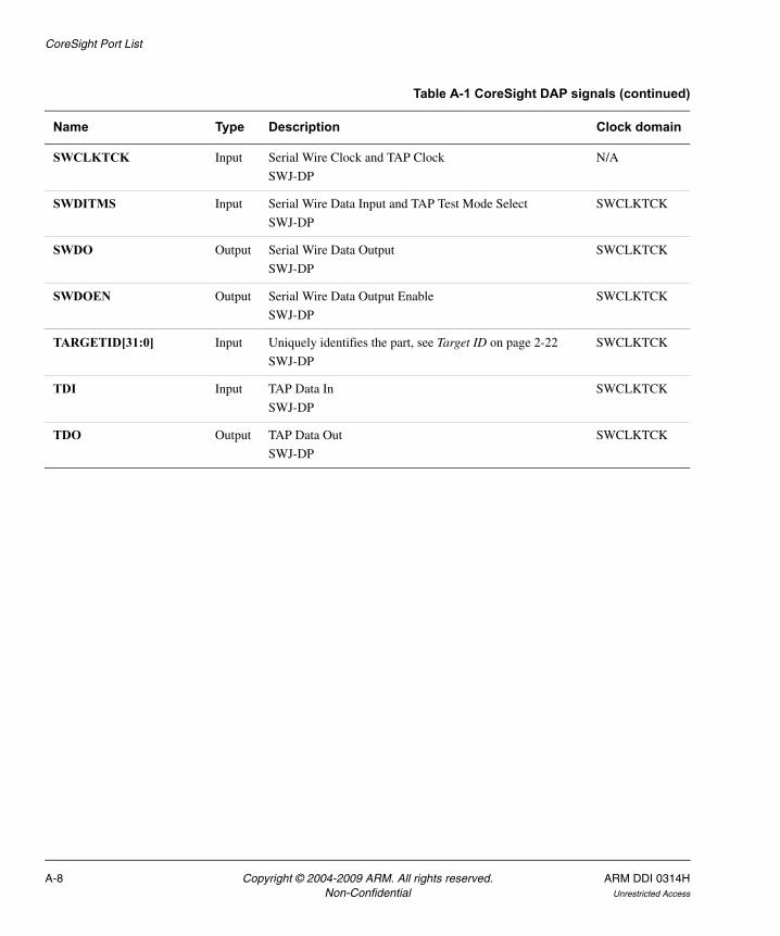
CoreSight Port List
SWCLKTCK Input Serial Wire Clock and TAP Clock
SWJ-DP
N/A
SWDITMS Input Serial Wire Data Input and TAP Test Mode Select
SWJ-DP
SWCLKTCK
SWDO Output Serial Wire Data Output
SWJ-DP
SWCLKTCK
SWDOEN Output Serial Wire Data Output Enable
SWJ-DP
SWCLKTCK
TARGETID[31:0] Input Uniquely identifies the part, see Target ID on page 2-22
SWJ-DP
SWCLKTCK
TDI Input TAP Data In
SWJ-DP
SWCLKTCK
TDO Output TAP Data Out
SWJ-DP
SWCLKTCK
Table A-1 CoreSight DAP signals (continued)
Name Type Description Clock domain
A-8 Copyright © 2004-2009 ARM. All rights reserved. ARM DDI 0314HNon-Confidential Unrestricted Access
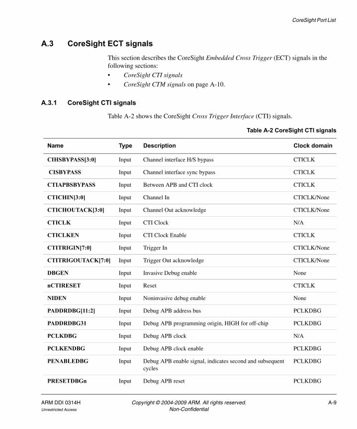
CoreSight Port List
A.3 CoreSight ECT signalsThis section describes the CoreSight Embedded Cross Trigger (ECT) signals in the following sections:
• CoreSight CTI signals
• CoreSight CTM signals on page A-10.
A.3.1 CoreSight CTI signals
Table A-2 shows the CoreSight Cross Trigger Interface (CTI) signals.
Table A-2 CoreSight CTI signals
Name Type Description Clock domain
CIHSBYPASS[3:0] Input Channel interface H/S bypass CTICLK
CISBYPASS Input Channel interface sync bypass CTICLK
CTIAPBSBYPASS Input Between APB and CTI clock CTICLK
CTICHIN[3:0] Input Channel In CTICLK/None
CTICHOUTACK[3:0] Input Channel Out acknowledge CTICLK/None
CTICLK Input CTI Clock N/A
CTICLKEN Input CTI Clock Enable CTICLK
CTITRIGIN[7:0] Input Trigger In CTICLK/None
CTITRIGOUTACK[7:0] Input Trigger Out acknowledge CTICLK/None
DBGEN Input Invasive Debug enable None
nCTIRESET Input Reset CTICLK
NIDEN Input Noninvasive debug enable None
PADDRDBG[11:2] Input Debug APB address bus PCLKDBG
PADDRDBG31 Input Debug APB programming origin, HIGH for off-chip PCLKDBG
PCLKDBG Input Debug APB clock N/A
PCLKENDBG Input Debug APB clock enable PCLKDBG
PENABLEDBG Input Debug APB enable signal, indicates second and subsequent cycles
PCLKDBG
PRESETDBGn Input Debug APB reset PCLKDBG
ARM DDI 0314H Copyright © 2004-2009 ARM. All rights reserved. A-9Unrestricted Access Non-Confidential
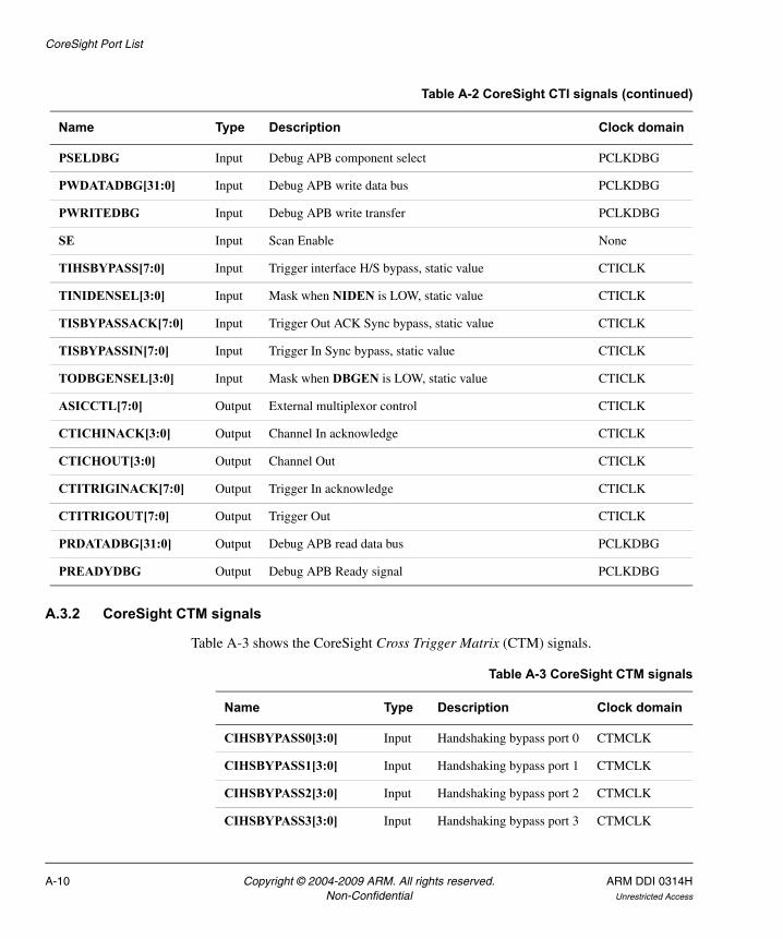
CoreSight Port List
A.3.2 CoreSight CTM signals
Table A-3 shows the CoreSight Cross Trigger Matrix (CTM) signals.
PSELDBG Input Debug APB component select PCLKDBG
PWDATADBG[31:0] Input Debug APB write data bus PCLKDBG
PWRITEDBG Input Debug APB write transfer PCLKDBG
SE Input Scan Enable None
TIHSBYPASS[7:0] Input Trigger interface H/S bypass, static value CTICLK
TINIDENSEL[3:0] Input Mask when NIDEN is LOW, static value CTICLK
TISBYPASSACK[7:0] Input Trigger Out ACK Sync bypass, static value CTICLK
TISBYPASSIN[7:0] Input Trigger In Sync bypass, static value CTICLK
TODBGENSEL[3:0] Input Mask when DBGEN is LOW, static value CTICLK
ASICCTL[7:0] Output External multiplexor control CTICLK
CTICHINACK[3:0] Output Channel In acknowledge CTICLK
CTICHOUT[3:0] Output Channel Out CTICLK
CTITRIGINACK[7:0] Output Trigger In acknowledge CTICLK
CTITRIGOUT[7:0] Output Trigger Out CTICLK
PRDATADBG[31:0] Output Debug APB read data bus PCLKDBG
PREADYDBG Output Debug APB Ready signal PCLKDBG
Table A-2 CoreSight CTI signals (continued)
Name Type Description Clock domain
Table A-3 CoreSight CTM signals
Name Type Description Clock domain
CIHSBYPASS0[3:0] Input Handshaking bypass port 0 CTMCLK
CIHSBYPASS1[3:0] Input Handshaking bypass port 1 CTMCLK
CIHSBYPASS2[3:0] Input Handshaking bypass port 2 CTMCLK
CIHSBYPASS3[3:0] Input Handshaking bypass port 3 CTMCLK
A-10 Copyright © 2004-2009 ARM. All rights reserved. ARM DDI 0314HNon-Confidential Unrestricted Access
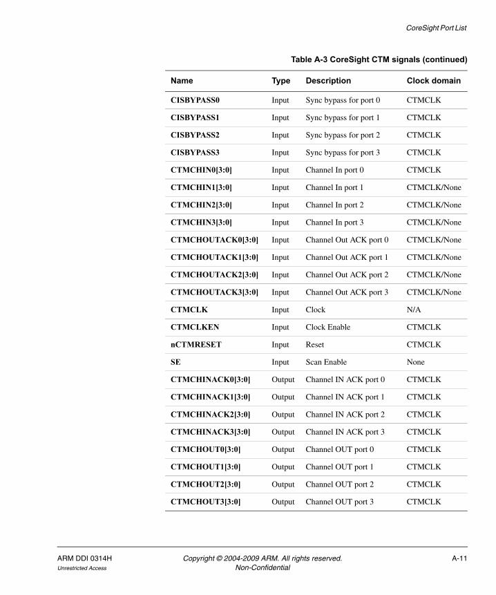
CoreSight Port List
CISBYPASS0 Input Sync bypass for port 0 CTMCLK
CISBYPASS1 Input Sync bypass for port 1 CTMCLK
CISBYPASS2 Input Sync bypass for port 2 CTMCLK
CISBYPASS3 Input Sync bypass for port 3 CTMCLK
CTMCHIN0[3:0] Input Channel In port 0 CTMCLK
CTMCHIN1[3:0] Input Channel In port 1 CTMCLK/None
CTMCHIN2[3:0] Input Channel In port 2 CTMCLK/None
CTMCHIN3[3:0] Input Channel In port 3 CTMCLK/None
CTMCHOUTACK0[3:0] Input Channel Out ACK port 0 CTMCLK/None
CTMCHOUTACK1[3:0] Input Channel Out ACK port 1 CTMCLK/None
CTMCHOUTACK2[3:0] Input Channel Out ACK port 2 CTMCLK/None
CTMCHOUTACK3[3:0] Input Channel Out ACK port 3 CTMCLK/None
CTMCLK Input Clock N/A
CTMCLKEN Input Clock Enable CTMCLK
nCTMRESET Input Reset CTMCLK
SE Input Scan Enable None
CTMCHINACK0[3:0] Output Channel IN ACK port 0 CTMCLK
CTMCHINACK1[3:0] Output Channel IN ACK port 1 CTMCLK
CTMCHINACK2[3:0] Output Channel IN ACK port 2 CTMCLK
CTMCHINACK3[3:0] Output Channel IN ACK port 3 CTMCLK
CTMCHOUT0[3:0] Output Channel OUT port 0 CTMCLK
CTMCHOUT1[3:0] Output Channel OUT port 1 CTMCLK
CTMCHOUT2[3:0] Output Channel OUT port 2 CTMCLK
CTMCHOUT3[3:0] Output Channel OUT port 3 CTMCLK
Table A-3 CoreSight CTM signals (continued)
Name Type Description Clock domain
ARM DDI 0314H Copyright © 2004-2009 ARM. All rights reserved. A-11Unrestricted Access Non-Confidential
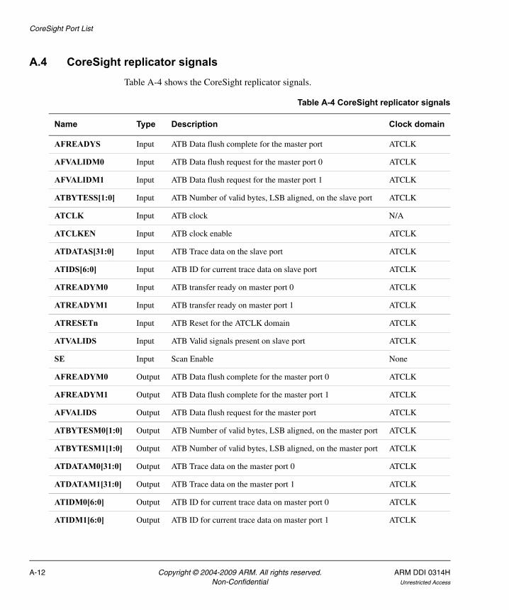
CoreSight Port List
A.4 CoreSight replicator signalsTable A-4 shows the CoreSight replicator signals.
Table A-4 CoreSight replicator signals
Name Type Description Clock domain
AFREADYS Input ATB Data flush complete for the master port ATCLK
AFVALIDM0 Input ATB Data flush request for the master port 0 ATCLK
AFVALIDM1 Input ATB Data flush request for the master port 1 ATCLK
ATBYTESS[1:0] Input ATB Number of valid bytes, LSB aligned, on the slave port ATCLK
ATCLK Input ATB clock N/A
ATCLKEN Input ATB clock enable ATCLK
ATDATAS[31:0] Input ATB Trace data on the slave port ATCLK
ATIDS[6:0] Input ATB ID for current trace data on slave port ATCLK
ATREADYM0 Input ATB transfer ready on master port 0 ATCLK
ATREADYM1 Input ATB transfer ready on master port 1 ATCLK
ATRESETn Input ATB Reset for the ATCLK domain ATCLK
ATVALIDS Input ATB Valid signals present on slave port ATCLK
SE Input Scan Enable None
AFREADYM0 Output ATB Data flush complete for the master port 0 ATCLK
AFREADYM1 Output ATB Data flush complete for the master port 1 ATCLK
AFVALIDS Output ATB Data flush request for the master port ATCLK
ATBYTESM0[1:0] Output ATB Number of valid bytes, LSB aligned, on the master port ATCLK
ATBYTESM1[1:0] Output ATB Number of valid bytes, LSB aligned, on the master port ATCLK
ATDATAM0[31:0] Output ATB Trace data on the master port 0 ATCLK
ATDATAM1[31:0] Output ATB Trace data on the master port 1 ATCLK
ATIDM0[6:0] Output ATB ID for current trace data on master port 0 ATCLK
ATIDM1[6:0] Output ATB ID for current trace data on master port 1 ATCLK
A-12 Copyright © 2004-2009 ARM. All rights reserved. ARM DDI 0314HNon-Confidential Unrestricted Access
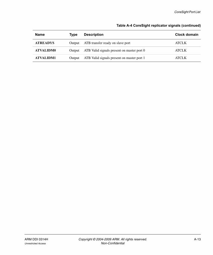
CoreSight Port List
ATREADYS Output ATB transfer ready on slave port ATCLK
ATVALIDM0 Output ATB Valid signals present on master port 0 ATCLK
ATVALIDM1 Output ATB Valid signals present on master port 1 ATCLK
Table A-4 CoreSight replicator signals (continued)
Name Type Description Clock domain
ARM DDI 0314H Copyright © 2004-2009 ARM. All rights reserved. A-13Unrestricted Access Non-Confidential
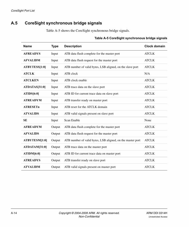
CoreSight Port List
A.5 CoreSight synchronous bridge signalsTable A-5 shows the CoreSight synchronous bridge signals.
Table A-5 CoreSight synchronous bridge signals
Name Type Description Clock domain
AFREADYS Input ATB data flush complete for the master port ATCLK
AFVALIDM Input ATB data flush request for the master port ATCLK
ATBYTESS[1:0] Input ATB number of valid bytes, LSB aligned, on the slave port ATCLK
ATCLK Input ATB clock N/A
ATCLKEN Input ATB clock enable ATCLK
ATDATAS[31:0] Input ATB trace data on the slave port ATCLK
ATIDS[6:0] Input ATB ID for current trace data on slave port ATCLK
ATREADYM Input ATB transfer ready on master port ATCLK
ATRESETn Input ATB reset for the ATCLK domain ATCLK
ATVALIDS Input ATB valid signals present on slave port ATCLK
SE Input Scan Enable None
AFREADYM Output ATB data flush complete for the master port ATCLK
AFVALIDS Output ATB data flush request for the master port ATCLK
ATBYTESM[1:0] Output ATB number of valid bytes, LSB aligned, on the master port ATCLK
ATDATAM[31:0] Output ATB trace data on the master port ATCLK
ATIDM[6:0] Output ATB ID for current trace data on master port ATCLK
ATREADYS Output ATB transfer ready on slave port ATCLK
ATVALIDM Output ATB valid signals present on master port ATCLK
A-14 Copyright © 2004-2009 ARM. All rights reserved. ARM DDI 0314HNon-Confidential Unrestricted Access

CoreSight Port List
A.6 CoreSight trace funnel signalsTable A-6 shows the CoreSight trace funnel signals.
Table A-6 CoreSight trace funnel signals
Name Type Description Clock domain
AFREADYS0 Input ATB Data flush complete for the slave port 0 ATCLK
AFREADYS1 Input ATB Data flush complete for the slave port 1 ATCLK
AFREADYS2 Input ATB Data flush complete for the slave port 2 ATCLK
AFREADYS3 Input ATB Data flush complete for the slave port 3 ATCLK
AFREADYS4 Input ATB Data flush complete for the slave port 4 ATCLK
AFREADYS5 Input ATB Data flush complete for the slave port 5 ATCLK
AFREADYS6 Input ATB Data flush complete for the slave port 6 ATCLK
AFREADYS7 Input ATB Data flush complete for the slave port 7 ATCLK
AFVALIDM Input ATB Data flush request for the master port ATCLK
ATBYTESS0[1:0] Input ATB Number of valid bytes, LSB aligned, on the slave port 0 ATCLK
ATBYTESS1[1:0] Input ATB Number of valid bytes, LSB aligned, on the slave port 1 ATCLK
ATBYTESS2[1:0] Input ATB Number of valid bytes, LSB aligned, on the slave port 2 ATCLK
ATBYTESS3[1:0] Input ATB Number of valid bytes, LSB aligned, on the slave port 3 ATCLK
ATBYTESS4[1:0] Input ATB Number of valid bytes, LSB aligned, on the slave port 4 ATCLK
ATBYTESS5[1:0] Input ATB Number of valid bytes, LSB aligned, on the slave port 5 ATCLK
ATBYTESS6[1:0] Input ATB Number of valid bytes, LSB aligned, on the slave port 6 ATCLK
ATBYTESS7[1:0] Input ATB Number of valid bytes, LSB aligned, on the slave port 7 ATCLK
ATCLK Input ATB clock N/A
ATCLKEN Input ATB clock enable ATCLK
ATDATAS0[31:0] Input ATB Trace data on the slave port 0 ATCLK
ATDATAS1[31:0] Input ATB Trace data on the slave port 1 ATCLK
ATDATAS2[31:0] Input ATB Trace data on the slave port 2 ATCLK
ATDATAS3[31:0] Input ATB Trace data on the slave port 3 ATCLK
ARM DDI 0314H Copyright © 2004-2009 ARM. All rights reserved. A-15Unrestricted Access Non-Confidential
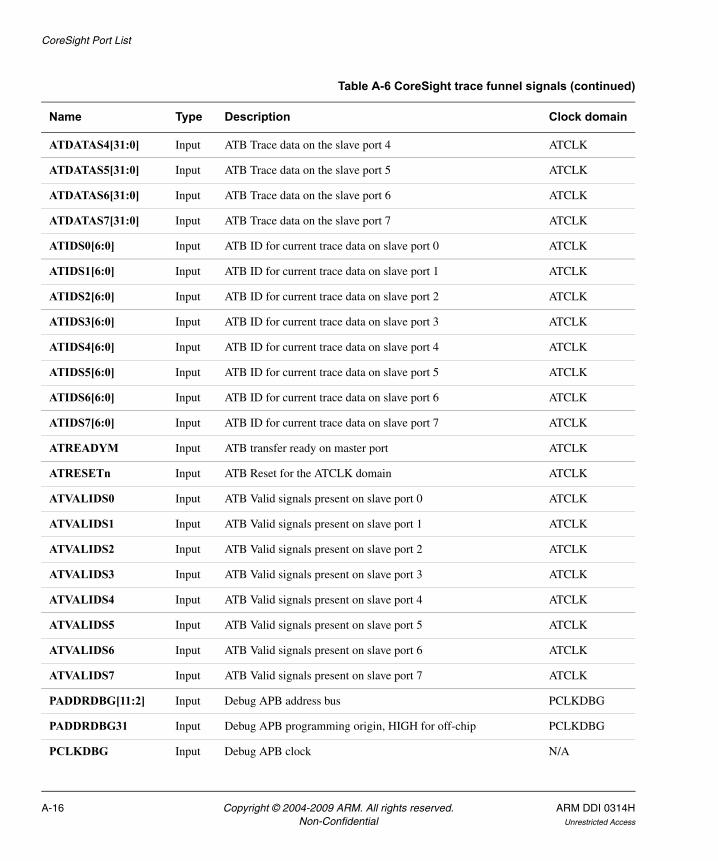
CoreSight Port List
ATDATAS4[31:0] Input ATB Trace data on the slave port 4 ATCLK
ATDATAS5[31:0] Input ATB Trace data on the slave port 5 ATCLK
ATDATAS6[31:0] Input ATB Trace data on the slave port 6 ATCLK
ATDATAS7[31:0] Input ATB Trace data on the slave port 7 ATCLK
ATIDS0[6:0] Input ATB ID for current trace data on slave port 0 ATCLK
ATIDS1[6:0] Input ATB ID for current trace data on slave port 1 ATCLK
ATIDS2[6:0] Input ATB ID for current trace data on slave port 2 ATCLK
ATIDS3[6:0] Input ATB ID for current trace data on slave port 3 ATCLK
ATIDS4[6:0] Input ATB ID for current trace data on slave port 4 ATCLK
ATIDS5[6:0] Input ATB ID for current trace data on slave port 5 ATCLK
ATIDS6[6:0] Input ATB ID for current trace data on slave port 6 ATCLK
ATIDS7[6:0] Input ATB ID for current trace data on slave port 7 ATCLK
ATREADYM Input ATB transfer ready on master port ATCLK
ATRESETn Input ATB Reset for the ATCLK domain ATCLK
ATVALIDS0 Input ATB Valid signals present on slave port 0 ATCLK
ATVALIDS1 Input ATB Valid signals present on slave port 1 ATCLK
ATVALIDS2 Input ATB Valid signals present on slave port 2 ATCLK
ATVALIDS3 Input ATB Valid signals present on slave port 3 ATCLK
ATVALIDS4 Input ATB Valid signals present on slave port 4 ATCLK
ATVALIDS5 Input ATB Valid signals present on slave port 5 ATCLK
ATVALIDS6 Input ATB Valid signals present on slave port 6 ATCLK
ATVALIDS7 Input ATB Valid signals present on slave port 7 ATCLK
PADDRDBG[11:2] Input Debug APB address bus PCLKDBG
PADDRDBG31 Input Debug APB programming origin, HIGH for off-chip PCLKDBG
PCLKDBG Input Debug APB clock N/A
Table A-6 CoreSight trace funnel signals (continued)
Name Type Description Clock domain
A-16 Copyright © 2004-2009 ARM. All rights reserved. ARM DDI 0314HNon-Confidential Unrestricted Access
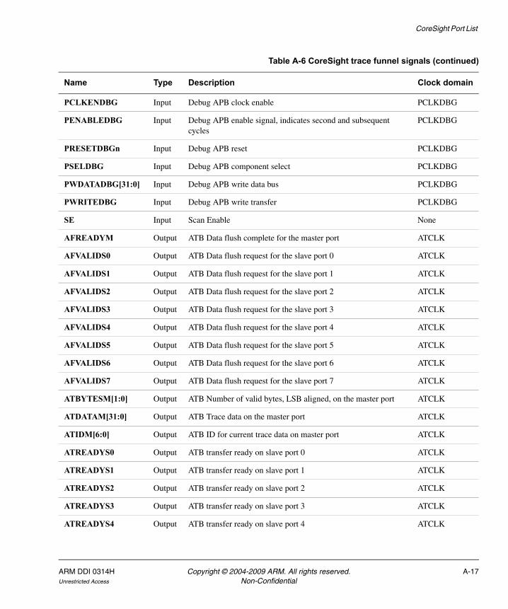
CoreSight Port List
PCLKENDBG Input Debug APB clock enable PCLKDBG
PENABLEDBG Input Debug APB enable signal, indicates second and subsequent cycles
PCLKDBG
PRESETDBGn Input Debug APB reset PCLKDBG
PSELDBG Input Debug APB component select PCLKDBG
PWDATADBG[31:0] Input Debug APB write data bus PCLKDBG
PWRITEDBG Input Debug APB write transfer PCLKDBG
SE Input Scan Enable None
AFREADYM Output ATB Data flush complete for the master port ATCLK
AFVALIDS0 Output ATB Data flush request for the slave port 0 ATCLK
AFVALIDS1 Output ATB Data flush request for the slave port 1 ATCLK
AFVALIDS2 Output ATB Data flush request for the slave port 2 ATCLK
AFVALIDS3 Output ATB Data flush request for the slave port 3 ATCLK
AFVALIDS4 Output ATB Data flush request for the slave port 4 ATCLK
AFVALIDS5 Output ATB Data flush request for the slave port 5 ATCLK
AFVALIDS6 Output ATB Data flush request for the slave port 6 ATCLK
AFVALIDS7 Output ATB Data flush request for the slave port 7 ATCLK
ATBYTESM[1:0] Output ATB Number of valid bytes, LSB aligned, on the master port ATCLK
ATDATAM[31:0] Output ATB Trace data on the master port ATCLK
ATIDM[6:0] Output ATB ID for current trace data on master port ATCLK
ATREADYS0 Output ATB transfer ready on slave port 0 ATCLK
ATREADYS1 Output ATB transfer ready on slave port 1 ATCLK
ATREADYS2 Output ATB transfer ready on slave port 2 ATCLK
ATREADYS3 Output ATB transfer ready on slave port 3 ATCLK
ATREADYS4 Output ATB transfer ready on slave port 4 ATCLK
Table A-6 CoreSight trace funnel signals (continued)
Name Type Description Clock domain
ARM DDI 0314H Copyright © 2004-2009 ARM. All rights reserved. A-17Unrestricted Access Non-Confidential
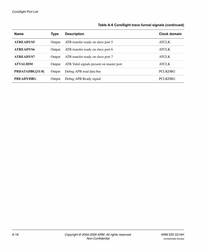
CoreSight Port List
ATREADYS5 Output ATB transfer ready on slave port 5 ATCLK
ATREADYS6 Output ATB transfer ready on slave port 6 ATCLK
ATREADYS7 Output ATB transfer ready on slave port 7 ATCLK
ATVALIDM Output ATB Valid signals present on master port ATCLK
PRDATADBG[31:0] Output Debug APB read data bus PCLKDBG
PREADYDBG Output Debug APB Ready signal PCLKDBG
Table A-6 CoreSight trace funnel signals (continued)
Name Type Description Clock domain
A-18 Copyright © 2004-2009 ARM. All rights reserved. ARM DDI 0314HNon-Confidential Unrestricted Access

CoreSight Port List
A.7 CoreSight TPIU signalsTable A-7 shows the CoreSight Trace Port Interface Unit (TPIU) signals.
Table A-7 CoreSight TPIU signals
Name Type Description Clock domain
AFREADYS Input ATB Data flush complete for the master port ATCLK
ATBYTESS[1:0] Input ATB Number of valid bytes, LSB aligned, on the slave port ATCLK
ATCLK Input ATB clock N/A
ATCLKEN Input ATB clock enable ATCLK
ATDATAS[31:0] Input ATB Trace data on the slave port ATCLK
ATIDS[6:0] Input ATB ID for current trace data on slave port ATCLK
ATRESETn Input ATB Reset for the ATCLK domain ATCLK
ATVALIDS Input ATB Valid signals present on slave port ATCLK
EXTCTLIN[7:0] Input External control input ATCLK
FLUSHIN Input Flush input from the CTI ATCLK/None
PADDRDBG[11:0] Input Debug APB address bus PCLKDBG
PADDRDBG31 Input Debug APB programming origin, HIGH for off-chip PCLKDBG
PCLKDBG Input Debug APB clock N/A
PCLKENDBG Input Debug APB clock enable PCLKDBG
PENABLEDBG Input Debug APB enable signal, indicates second and subsequent cycles
PCLKDBG
PRESETDBGn Input Debug APB reset PCLKDBG
PSELDBG Input Debug APB component select PCLKDBG
PWDATADBG[31:0] Input Debug APB write data bus PCLKDBG
PWRITEDBG Input Debug APB write transfer PCLKDBG
SE Input Scan Enable None
TPCTL Input Tie-off to report presence of TRACECTL, static value ATCLK
TPMAXDATASIZE[4:0]
Input Tie-off to report maximum number of pins on TRACEDATA, static value
ATCLK
ARM DDI 0314H Copyright © 2004-2009 ARM. All rights reserved. A-19Unrestricted Access Non-Confidential
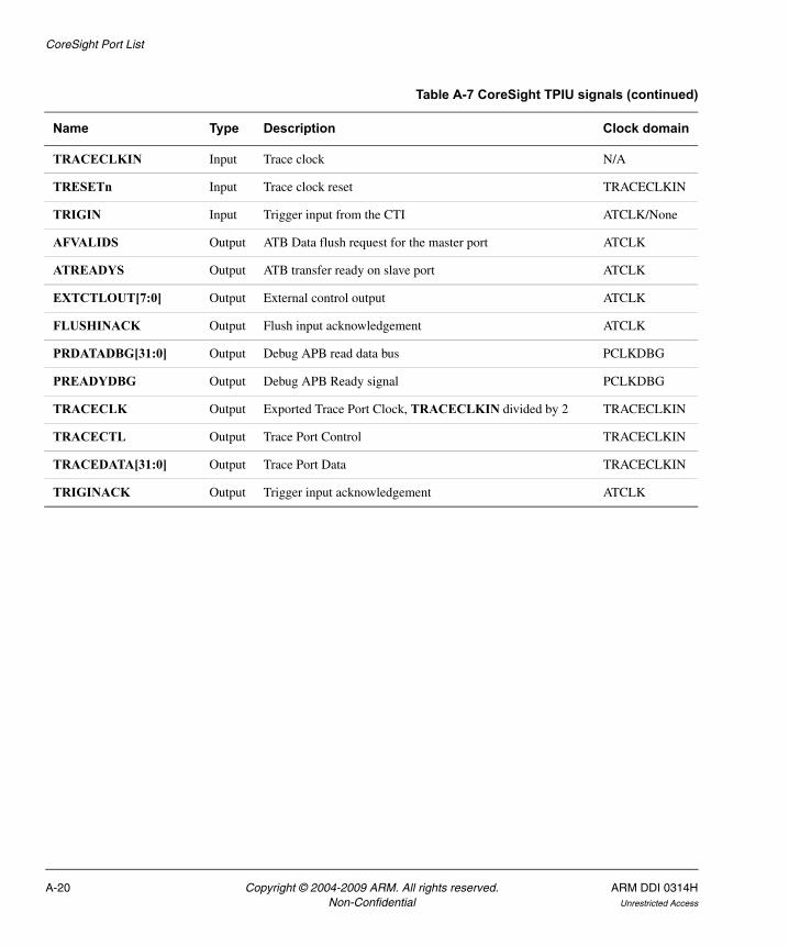
CoreSight Port List
TRACECLKIN Input Trace clock N/A
TRESETn Input Trace clock reset TRACECLKIN
TRIGIN Input Trigger input from the CTI ATCLK/None
AFVALIDS Output ATB Data flush request for the master port ATCLK
ATREADYS Output ATB transfer ready on slave port ATCLK
EXTCTLOUT[7:0] Output External control output ATCLK
FLUSHINACK Output Flush input acknowledgement ATCLK
PRDATADBG[31:0] Output Debug APB read data bus PCLKDBG
PREADYDBG Output Debug APB Ready signal PCLKDBG
TRACECLK Output Exported Trace Port Clock, TRACECLKIN divided by 2 TRACECLKIN
TRACECTL Output Trace Port Control TRACECLKIN
TRACEDATA[31:0] Output Trace Port Data TRACECLKIN
TRIGINACK Output Trigger input acknowledgement ATCLK
Table A-7 CoreSight TPIU signals (continued)
Name Type Description Clock domain
A-20 Copyright © 2004-2009 ARM. All rights reserved. ARM DDI 0314HNon-Confidential Unrestricted Access
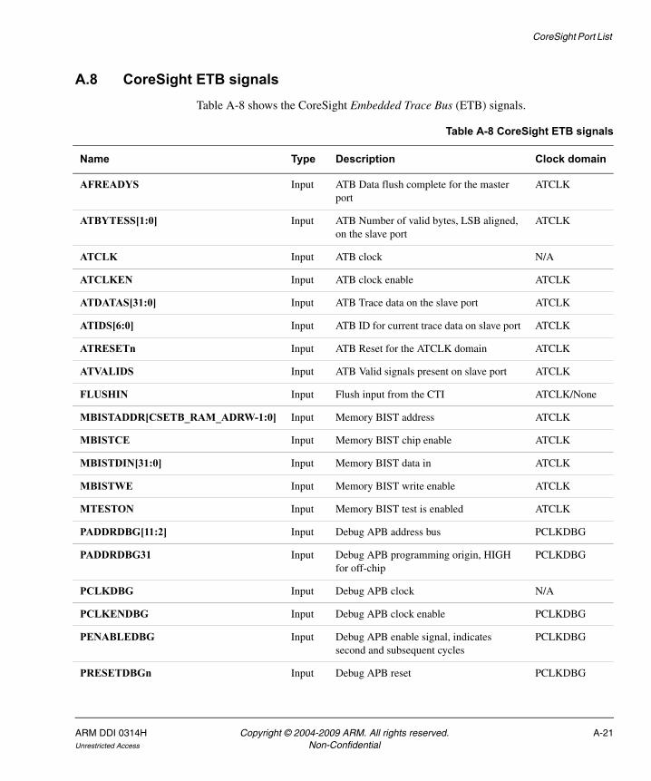
CoreSight Port List
A.8 CoreSight ETB signalsTable A-8 shows the CoreSight Embedded Trace Bus (ETB) signals.
Table A-8 CoreSight ETB signals
Name Type Description Clock domain
AFREADYS Input ATB Data flush complete for the master port
ATCLK
ATBYTESS[1:0] Input ATB Number of valid bytes, LSB aligned, on the slave port
ATCLK
ATCLK Input ATB clock N/A
ATCLKEN Input ATB clock enable ATCLK
ATDATAS[31:0] Input ATB Trace data on the slave port ATCLK
ATIDS[6:0] Input ATB ID for current trace data on slave port ATCLK
ATRESETn Input ATB Reset for the ATCLK domain ATCLK
ATVALIDS Input ATB Valid signals present on slave port ATCLK
FLUSHIN Input Flush input from the CTI ATCLK/None
MBISTADDR[CSETB_RAM_ADRW-1:0] Input Memory BIST address ATCLK
MBISTCE Input Memory BIST chip enable ATCLK
MBISTDIN[31:0] Input Memory BIST data in ATCLK
MBISTWE Input Memory BIST write enable ATCLK
MTESTON Input Memory BIST test is enabled ATCLK
PADDRDBG[11:2] Input Debug APB address bus PCLKDBG
PADDRDBG31 Input Debug APB programming origin, HIGH for off-chip
PCLKDBG
PCLKDBG Input Debug APB clock N/A
PCLKENDBG Input Debug APB clock enable PCLKDBG
PENABLEDBG Input Debug APB enable signal, indicates second and subsequent cycles
PCLKDBG
PRESETDBGn Input Debug APB reset PCLKDBG
ARM DDI 0314H Copyright © 2004-2009 ARM. All rights reserved. A-21Unrestricted Access Non-Confidential
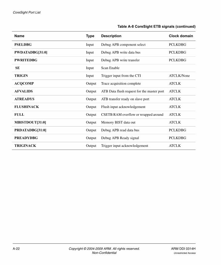
CoreSight Port List
PSELDBG Input Debug APB component select PCLKDBG
PWDATADBG[31:0] Input Debug APB write data bus PCLKDBG
PWRITEDBG Input Debug APB write transfer PCLKDBG
SE Input Scan Enable
TRIGIN Input Trigger input from the CTI ATCLK/None
ACQCOMP Output Trace acquisition complete ATCLK
AFVALIDS Output ATB Data flush request for the master port ATCLK
ATREADYS Output ATB transfer ready on slave port ATCLK
FLUSHINACK Output Flush input acknowledgement ATCLK
FULL Output CSETB RAM overflow or wrapped around ATCLK
MBISTDOUT[31:0] Output Memory BIST data out ATCLK
PRDATADBG[31:0] Output Debug APB read data bus PCLKDBG
PREADYDBG Output Debug APB Ready signal PCLKDBG
TRIGINACK Output Trigger input acknowledgement ATCLK
Table A-8 CoreSight ETB signals (continued)
Name Type Description Clock domain
A-22 Copyright © 2004-2009 ARM. All rights reserved. ARM DDI 0314HNon-Confidential Unrestricted Access
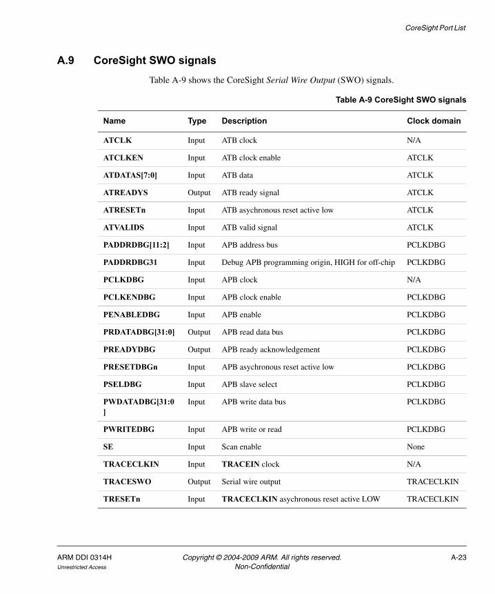
CoreSight Port List
A.9 CoreSight SWO signalsTable A-9 shows the CoreSight Serial Wire Output (SWO) signals.
Table A-9 CoreSight SWO signals
Name Type Description Clock domain
ATCLK Input ATB clock N/A
ATCLKEN Input ATB clock enable ATCLK
ATDATAS[7:0] Input ATB data ATCLK
ATREADYS Output ATB ready signal ATCLK
ATRESETn Input ATB asychronous reset active low ATCLK
ATVALIDS Input ATB valid signal ATCLK
PADDRDBG[11:2] Input APB address bus PCLKDBG
PADDRDBG31 Input Debug APB programming origin, HIGH for off-chip PCLKDBG
PCLKDBG Input APB clock N/A
PCLKENDBG Input APB clock enable PCLKDBG
PENABLEDBG Input APB enable PCLKDBG
PRDATADBG[31:0] Output APB read data bus PCLKDBG
PREADYDBG Output APB ready acknowledgement PCLKDBG
PRESETDBGn Input APB asychronous reset active low PCLKDBG
PSELDBG Input APB slave select PCLKDBG
PWDATADBG[31:0]
Input APB write data bus PCLKDBG
PWRITEDBG Input APB write or read PCLKDBG
SE Input Scan enable None
TRACECLKIN Input TRACEIN clock N/A
TRACESWO Output Serial wire output TRACECLKIN
TRESETn Input TRACECLKIN asychronous reset active LOW TRACECLKIN
ARM DDI 0314H Copyright © 2004-2009 ARM. All rights reserved. A-23Unrestricted Access Non-Confidential
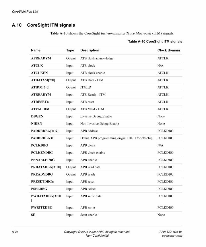
CoreSight Port List
A.10 CoreSight ITM signalsTable A-10 shows the CoreSight Instrumentation Trace Macrocell (ITM) signals.
Table A-10 CoreSight ITM signals
Name Type Description Clock domain
AFREADYM Output ATB flush acknowledge ATCLK
ATCLK Input ATB clock N/A
ATCLKEN Input ATB clock enable ATCLK
ATDATAM[7:0] Output ATB Data - ITM ATCLK
ATIDM[6:0] Output ITM ID ATCLK
ATREADYM Input ATB Ready - ITM ATCLK
ATRESETn Input ATB reset ATCLK
ATVALIDM Output ATB Valid - ITM ATCLK
DBGEN Input Invasive Debug Enable None
NIDEN Input Non-Invasive Debug Enable None
PADDRDBG[11:2] Input APB address PCLKDBG
PADDRDBG31 Input Debug APB programming origin, HIGH for off-chip PCLKDBG
PCLKDBG Input APB clock N/A
PCLKENDBG Input APB clock enable PCLKDBG
PENABLEDBG Input APB enable PCLKDBG
PRDATADBG[31:0] Output APB read data PCLKDBG
PREADYDBG Output APB ready PCLKDBG
PRESETDBGn Input APB reset PCLKDBG
PSELDBG Input APB select PCLKDBG
PWDATADBG[31:0]
Input APB write data PCLKDBG
PWRITEDBG Input APB write PCLKDBG
SE Input Scan enable None
A-24 Copyright © 2004-2009 ARM. All rights reserved. ARM DDI 0314HNon-Confidential Unrestricted Access

CoreSight Port List
SPIDEN Input Secure Invasive Debug Enable None
SPNIDEN Input Secure Non-Invasive Debug Enable None
TRIGOUT Output Indicates a trigger event ATCLK
TRIGOUTACK Input TRIGOUT acknowledgement ATCLK
Table A-10 CoreSight ITM signals (continued)
Name Type Description Clock domain
ARM DDI 0314H Copyright © 2004-2009 ARM. All rights reserved. A-25Unrestricted Access Non-Confidential

CoreSight Port List
A-26 Copyright © 2004-2009 ARM. All rights reserved. ARM DDI 0314HNon-Confidential Unrestricted Access
Appendix B CoreSight Components and Clock Domains
This appendix lists CoreSight components and their clock domains. It contains the following section:
• CoreSight components and clock domains on page B-2.
ARM DDI 0314H Copyright © 2004-2009 ARM. All rights reserved. B-1Unrestricted Access Non-Confidential
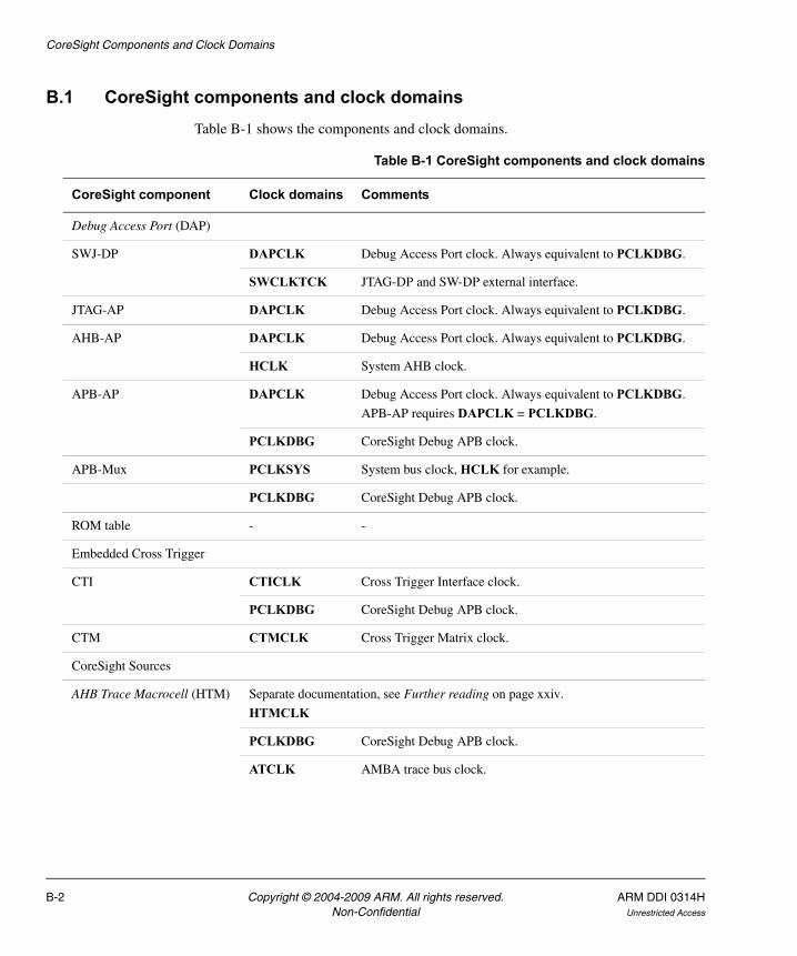
CoreSight Components and Clock Domains
B.1 CoreSight components and clock domainsTable B-1 shows the components and clock domains.
Table B-1 CoreSight components and clock domains
CoreSight component Clock domains Comments
Debug Access Port (DAP)
SWJ-DP DAPCLK Debug Access Port clock. Always equivalent to PCLKDBG.
SWCLKTCK JTAG-DP and SW-DP external interface.
JTAG-AP DAPCLK Debug Access Port clock. Always equivalent to PCLKDBG.
AHB-AP DAPCLK Debug Access Port clock. Always equivalent to PCLKDBG.
HCLK System AHB clock.
APB-AP DAPCLK Debug Access Port clock. Always equivalent to PCLKDBG.
APB-AP requires DAPCLK = PCLKDBG.
PCLKDBG CoreSight Debug APB clock.
APB-Mux PCLKSYS System bus clock, HCLK for example.
PCLKDBG CoreSight Debug APB clock.
ROM table - -
Embedded Cross Trigger
CTI CTICLK Cross Trigger Interface clock.
PCLKDBG CoreSight Debug APB clock.
CTM CTMCLK Cross Trigger Matrix clock.
CoreSight Sources
AHB Trace Macrocell (HTM) Separate documentation, see Further reading on page xxiv.
HTMCLK
PCLKDBG CoreSight Debug APB clock.
ATCLK AMBA trace bus clock.
B-2 Copyright © 2004-2009 ARM. All rights reserved. ARM DDI 0314HNon-Confidential Unrestricted Access
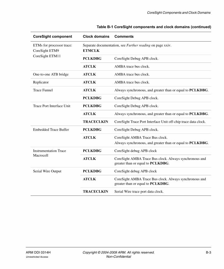
CoreSight Components and Clock Domains
ETMs for processor trace:
CoreSight ETM9
CoreSight ETM11
Separate documentation, see Further reading on page xxiv.
ETMCLK
PCLKDBG CoreSight Debug APB clock.
ATCLK AMBA trace bus clock.
One-to-one ATB bridge ATCLK AMBA trace bus clock.
Replicator ATCLK AMBA trace bus clock.
Trace Funnel ATCLK Always synchronous, and greater than or equal to PCLKDBG.
PCLKDBG CoreSight Debug APB clock.
Trace Port Interface Unit PCLKDBG CoreSight Debug APB clock.
ATCLK Always synchronous, and greater than or equal to PCLKDBG.
TRACECLKIN CoreSight Trace Port Interface Unit off-chip trace data clock.
Embedded Trace Buffer PCLKDBG CoreSight Debug APB clock.
ATCLK CoreSight AMBA Trace Bus clock.
Always synchronous, and greater than or equal to PCLKDBG.
Instrumentation Trace Macrocell
PCLKDBG CoreSight debug APB clock
ATCLK CoreSight AMBA Trace Bus clock. Always synchronous and greater than or equal to PCLKDBG.
Serial Wire Output PCLKDBG CoreSight debug APB clock
ATCLK CoreSight AMBA Trace Bus clock. Always synchronous and greater than or equal to PCLKDBG.
TRACECLKIN Serial Wire trace port data clock.
Table B-1 CoreSight components and clock domains (continued)
CoreSight component Clock domains Comments
ARM DDI 0314H Copyright © 2004-2009 ARM. All rights reserved. B-3Unrestricted Access Non-Confidential

CoreSight Components and Clock Domains
B-4 Copyright © 2004-2009 ARM. All rights reserved. ARM DDI 0314HNon-Confidential Unrestricted Access
Appendix C Serial Wire Debug and JTAG Trace Connector
This appendix describes the SWD and JTAG trace connector. It contains the following sections:
• About the SWD and JTAG trace connector on page C-2
• Pinout details on page C-3
• Signal definitions on page C-8.
ARM DDI 0314H Copyright © 2004-2009 ARM. All rights reserved. C-1Unrestricted Access Non-Confidential
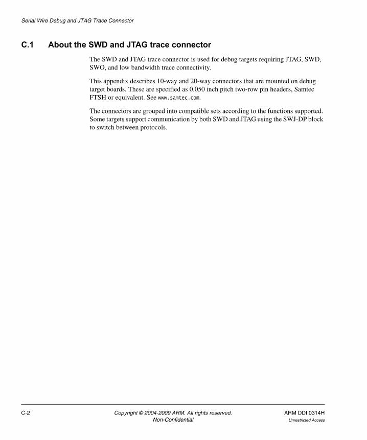
Serial Wire Debug and JTAG Trace Connector
C.1 About the SWD and JTAG trace connectorThe SWD and JTAG trace connector is used for debug targets requiring JTAG, SWD, SWO, and low bandwidth trace connectivity.
This appendix describes 10-way and 20-way connectors that are mounted on debug target boards. These are specified as 0.050 inch pitch two-row pin headers, Samtec FTSH or equivalent. See www.samtec.com.
The connectors are grouped into compatible sets according to the functions supported. Some targets support communication by both SWD and JTAG using the SWJ-DP block to switch between protocols.
C-2 Copyright © 2004-2009 ARM. All rights reserved. ARM DDI 0314HNon-Confidential Unrestricted Access

Serial Wire Debug and JTAG Trace Connector
C.2 Pinout detailsThe connector pin layouts are described in:
• Combined pin names
• 10-way connector pinouts on page C-5
• 20-way connector pinouts including trace on page C-6.
Note The equivalent pin numbers on a CoreSight-compatible Mictor connector pinout are shown in the tables. This enables you to build a target where the debug communication signals are brought in parallel to both connectors so that the target can be debugged using either physical connector.
C.2.1 Combined pin names
Table C-1 shows a summary of the pin names.
See Table C-4 on page C-8 for a generic description of the pins.
The following sections describe the use of pins 6, 8, 11, and 13:
• EXTa and EXTb pins on page C-4
• GND/TgtPwr+Cap pins on page C-4.
Table C-1 Summary of pin names
Pin number Combined pin name Pin number Combined pin name
1 VTref 11 Gnd/TgtPwr+Cap
2 TMS/SWDIO 12 TraceClk/RTCK
3 GND 13 Gnd/TgtPwr+Cap
4 TCK/SWCLK 14 TraceD0/SWO
5 GND 15 GND
6 TDO/SWO/EXTa/TraceCtl 16 TraceD1/nTRST
7 Key 17 GND
8 TDI/EXTb/TraceCtl 18 TraceD2/TrigIn
9 GNDDetect 19 GND
10 TraceCtl/nRESET 20 TraceD3/TrigOut
ARM DDI 0314H Copyright © 2004-2009 ARM. All rights reserved. C-3Unrestricted Access Non-Confidential
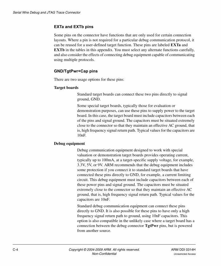
Serial Wire Debug and JTAG Trace Connector
EXTa and EXTb pins
Some pins on the connector have functions that are only used for certain connection layouts. Where a pin is not required for a particular debug communication protocol, it can be reused for a user-defined target function. These pins are labeled EXTa and EXTb in the tables in this appendix. You must select any alternate functions carefully, and also consider the effects of connecting debug equipment capable of communicating using multiple protocols.
GND/TgtPwr+Cap pins
There are two usage options for these pins:
Target boards
Standard target boards can connect these two pins directly to signal ground, GND.
Some special target boards, typically those for evaluation or demonstration purposes, can use these pins to supply power to the target board. In this case, the target board must include capacitors between each of the pins and signal ground. The capacitors must be situated extremely close to the connector so that they maintain an effective AC ground, that is, high frequency signal return path. Typical values for the capacitors are 10nF.
Debug equipment
Debug communication equipment designed to work with special valuation or demonstration target boards provides operating current, typically up to 100mA, at a target-specific supply voltage, for example, 3.3V, 5V, or 9V. ARM recommends that the debug equipment includes some protection if you connect it to standard target boards that have connected these pins directly to GND, for example, a current limiting circuit. This debug equipment must include capacitors between each of these power pins and signal ground. The capacitors must be situated extremely close to the connector so that they maintain an effective AC ground, that is, high frequency signal return path. Typical values for the capacitors are 10nF.
Standard debug communication equipment can connect these pins directly to GND. It is also possible for these pins to have only a high frequency signal return path to ground, using 10nF capacitors. This option is also compatible in the unlikely case where a target board has a connection between the debug connector TgtPwr pins, but is powered from another source.
C-4 Copyright © 2004-2009 ARM. All rights reserved. ARM DDI 0314HNon-Confidential Unrestricted Access
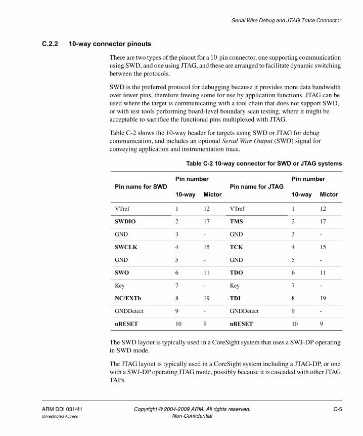
Serial Wire Debug and JTAG Trace Connector
C.2.2 10-way connector pinouts
There are two types of the pinout for a 10-pin connector, one supporting communication using SWD, and one using JTAG, and these are arranged to facilitate dynamic switching between the protocols.
SWD is the preferred protocol for debugging because it provides more data bandwidth over fewer pins, therefore freeing some for use by application functions. JTAG can be used where the target is communicating with a tool chain that does not support SWD, or with test tools performing board-level boundary scan testing, where it might be acceptable to sacrifice the functional pins multiplexed with JTAG.
Table C-2 shows the 10-way header for targets using SWD or JTAG for debug communication, and includes an optional Serial Wire Output (SWO) signal for conveying application and instrumentation trace.
The SWD layout is typically used in a CoreSight system that uses a SWJ-DP operating in SWD mode.
The JTAG layout is typically used in a CoreSight system including a JTAG-DP, or one with a SWJ-DP operating JTAG mode, possibly because it is cascaded with other JTAG TAPs.
Table C-2 10-way connector for SWD or JTAG systems
Pin name for SWDPin number
Pin name for JTAGPin number
10-way Mictor 10-way Mictor
VTref 1 12 VTref 1 12
SWDIO 2 17 TMS 2 17
GND 3 - GND 3 -
SWCLK 4 15 TCK 4 15
GND 5 - GND 5 -
SWO 6 11 TDO 6 11
Key 7 - Key 7 -
NC/EXTb 8 19 TDI 8 19
GNDDetect 9 - GNDDetect 9 -
nRESET 10 9 nRESET 10 9
ARM DDI 0314H Copyright © 2004-2009 ARM. All rights reserved. C-5Unrestricted Access Non-Confidential
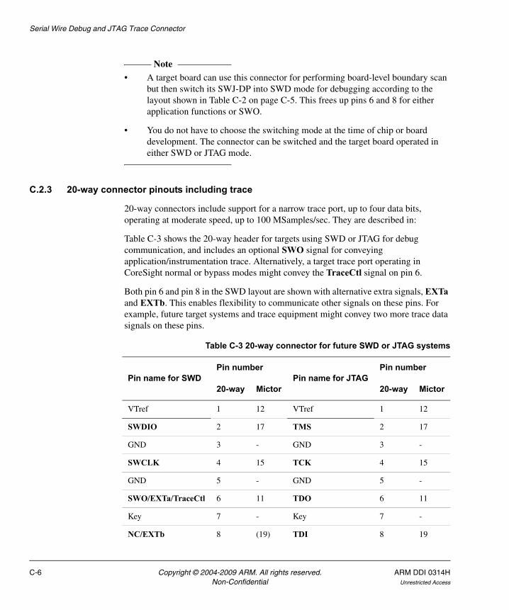
Serial Wire Debug and JTAG Trace Connector
Note • A target board can use this connector for performing board-level boundary scan
but then switch its SWJ-DP into SWD mode for debugging according to the layout shown in Table C-2 on page C-5. This frees up pins 6 and 8 for either application functions or SWO.
• You do not have to choose the switching mode at the time of chip or board development. The connector can be switched and the target board operated in either SWD or JTAG mode.
C.2.3 20-way connector pinouts including trace
20-way connectors include support for a narrow trace port, up to four data bits, operating at moderate speed, up to 100 MSamples/sec. They are described in:
Table C-3 shows the 20-way header for targets using SWD or JTAG for debug communication, and includes an optional SWO signal for conveying application/instrumentation trace. Alternatively, a target trace port operating in CoreSight normal or bypass modes might convey the TraceCtl signal on pin 6.
Both pin 6 and pin 8 in the SWD layout are shown with alternative extra signals, EXTa and EXTb. This enables flexibility to communicate other signals on these pins. For example, future target systems and trace equipment might convey two more trace data signals on these pins.
Table C-3 20-way connector for future SWD or JTAG systems
Pin name for SWDPin number
Pin name for JTAGPin number
20-way Mictor 20-way Mictor
VTref 1 12 VTref 1 12
SWDIO 2 17 TMS 2 17
GND 3 - GND 3 -
SWCLK 4 15 TCK 4 15
GND 5 - GND 5 -
SWO/EXTa/TraceCtl 6 11 TDO 6 11
Key 7 - Key 7 -
NC/EXTb 8 (19) TDI 8 19
C-6 Copyright © 2004-2009 ARM. All rights reserved. ARM DDI 0314HNon-Confidential Unrestricted Access
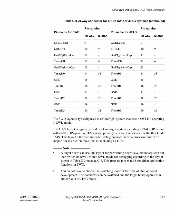
Serial Wire Debug and JTAG Trace Connector
The SWD layout is typically used in a CoreSight system that uses a SWJ-DP operating in SWD mode.
The JTAG layout is typically used in a CoreSight system including a JTAG-DP, or one with a SWJ-DP operating JTAG mode, possibly because it is cascaded with other JTAG TAPs. This layout s the recommended debug connection for a processor built with support for instruction trace, that is, including an ETM.
Note • A target board can use this layout for performing board-level boundary scan but
then switch its SWJ-DP into SWD mode for debugging according to the layout shown in Table C-3 on page C-6. This frees up pins 6 and 8 for either application functions or SWO.
• You do not have to choose the switching mode at the time of chip or board development. The connector can be switched and the target board operated in either SWD or JTAG mode.
GNDDetect 9 - GNDDetect 9 -
nRESET 10 9 nRESET 10 9
Gnd/TgtPwr+Cap 11 - Gnd/TgtPwr+Cap 11 -
TraceClk 12 6 TraceClk 12 6
Gnd/TgtPwr+Cap 13 - Gnd/TgtPwr+Cap 13 -
TraceD0 14 38 TraceD0 14 38
GND 15 - GND 15 -
TraceD1 16 28 TraceD1 16 28
GND 17 - GND 17 -
TraceD2 18 26 TraceD2 18 26
GND 19 - GND 19 -
TraceD3 20 24 TraceD3 20 24
Table C-3 20-way connector for future SWD or JTAG systems (continued)
Pin name for SWDPin number
Pin name for JTAGPin number
20-way Mictor 20-way Mictor
ARM DDI 0314H Copyright © 2004-2009 ARM. All rights reserved. C-7Unrestricted Access Non-Confidential

Serial Wire Debug and JTAG Trace Connector
C.3 Signal definitionsTable C-4 shows the generic trace connector signal definitions.
Note See Combined pin names on page C-3 for information on how these signals are used in the SWD and JTAG trace connector.
Table C-4 Generic signal definitions
Signal Type Description
VTref Output Debug and trace port reference voltage.
TMS Input Standard JTAG pin.
TCK Input Standard JTAG pin.
TDO Output User-definable JTAG pin.
Key - Key pin. Removed from target connector, or physically blocked on debug connector.
TDI Input User-definable JTAG pin.
GndDetect - Can be used by target system for debugger presence detection.
nRESET - Target reset signal.
TraceClk Output Clock trace pin.
TraceD[n] Output Trace data pins.
C-8 Copyright © 2004-2009 ARM. All rights reserved. ARM DDI 0314HNon-Confidential Unrestricted Access
Appendix D Deprecated SWJ-DP Switching Sequences
This appendix describes the switching sequences used in earlier versions of the Serial Wire JTAG Debug Port (SWJ-DP). It contains the following section:
• About the deprecated SWJ-DP switching sequences on page D-2.
ARM DDI 0314H Copyright © 2004-2009 ARM. All rights reserved. D-1Unrestricted Access Non-Confidential
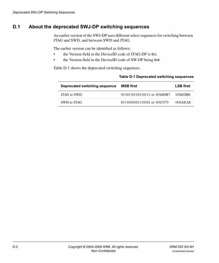
Deprecated SWJ-DP Switching Sequences
D.1 About the deprecated SWJ-DP switching sequencesAn earlier version of the SWJ-DP uses different select sequences for switching between JTAG and SWD, and between SWD and JTAG.
The earlier version can be identified as follows:
• the Version field in the DeviceID code of JTAG-DP is 0x1
• the Version field in the DeviceID code of SW-DP being 0x0.
Table D-1 shows the deprecated switching sequences.
Table D-1 Deprecated switching sequences
Deprecated switching sequence MSB first LSB first
JTAG to SWD 0110110110110111 or 16'h6DB7 16'hEDB6
SWD to JTAG 0111010101110101 or 16'h7575 16'hAEAE
D-2 Copyright © 2004-2009 ARM. All rights reserved. ARM DDI 0314HNon-Confidential Unrestricted Access
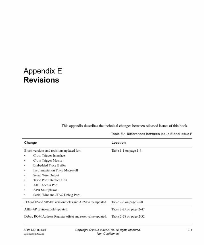
Appendix E Revisions
This appendix describes the technical changes between released issues of this book.
Table E-1 Differences between issue E and issue F
Change Location
Block versions and revisions updated for:
• Cross Trigger Interface
• Cross Trigger Matrix
• Embedded Trace Buffer
• Instrumentation Trace Macrocell
• Serial Wire Output
• Trace Port Interface Unit
• AHB Access Port
• APB Multiplexor
• Serial Wire and JTAG Debug Port.
Table 1-1 on page 1-4
JTAG-DP and SW-DP version fields and ARM value updated. Table 2-8 on page 2-28
AHB-AP revision field updated. Table 2-25 on page 2-47
Debug ROM Address Register offset and reset value updated. Table 2-28 on page 2-52
ARM DDI 0314H Copyright © 2004-2009 ARM. All rights reserved. E-1Unrestricted Access Non-Confidential
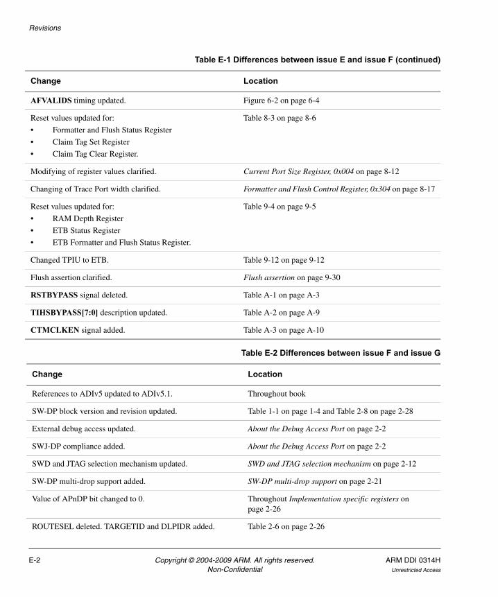
Revisions
AFVALIDS timing updated. Figure 6-2 on page 6-4
Reset values updated for:
• Formatter and Flush Status Register
• Claim Tag Set Register
• Claim Tag Clear Register.
Table 8-3 on page 8-6
Modifying of register values clarified. Current Port Size Register, 0x004 on page 8-12
Changing of Trace Port width clarified. Formatter and Flush Control Register, 0x304 on page 8-17
Reset values updated for:
• RAM Depth Register
• ETB Status Register
• ETB Formatter and Flush Status Register.
Table 9-4 on page 9-5
Changed TPIU to ETB. Table 9-12 on page 9-12
Flush assertion clarified. Flush assertion on page 9-30
RSTBYPASS signal deleted. Table A-1 on page A-3
TIHSBYPASS[7:0] description updated. Table A-2 on page A-9
CTMCLKEN signal added. Table A-3 on page A-10
Table E-2 Differences between issue F and issue G
Change Location
References to ADIv5 updated to ADIv5.1. Throughout book
SW-DP block version and revision updated. Table 1-1 on page 1-4 and Table 2-8 on page 2-28
External debug access updated. About the Debug Access Port on page 2-2
SWJ-DP compliance added. About the Debug Access Port on page 2-2
SWD and JTAG selection mechanism updated. SWD and JTAG selection mechanism on page 2-12
SW-DP multi-drop support added. SW-DP multi-drop support on page 2-21
Value of APnDP bit changed to 0. Throughout Implementation specific registers on page 2-26
ROUTESEL deleted. TARGETID and DLPIDR added. Table 2-6 on page 2-26
Table E-1 Differences between issue E and issue F (continued)
Change Location
E-2 Copyright © 2004-2009 ARM. All rights reserved. ARM DDI 0314HNon-Confidential Unrestricted Access
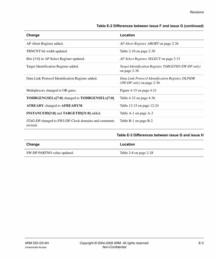
Revisions
AP Abort Register added. AP Abort Register, ABORT on page 2-26
TRNCNT bit width updated. Table 2-10 on page 2-30
Bits [3:0] in AP Select Register updated. AP Select Register, SELECT on page 2-31
Target Identification Register added. Target Identification Register, TARGETID (SW-DP only) on page 2-36
Data Link Protocol Identification Register added. Data Link Protocol Identification Register, DLPIDR (SW-DP only) on page 2-36
Multiplexors changed to OR gates. Figure 4-15 on page 4-21
TODBGENGSELx[7:0] changed to TODBGENSELx[7:0]. Table 4-32 on page 4-36
ATREADY changed to AFREADYM. Table 12-15 on page 12-24
INSTANCEID[3:0] and TARGETID[31:0] added. Table A-1 on page A-3
JTAG-DP changed to SWJ-DP. Clock domains and comments revised.
Table B-1 on page B-2
Table E-3 Differences between issue G and issue H
Change Location
SW-DP PARTNO value updated. Table 2-8 on page 2-28
Table E-2 Differences between issue F and issue G (continued)
Change Location
ARM DDI 0314H Copyright © 2004-2009 ARM. All rights reserved. E-3Unrestricted Access Non-Confidential

Revisions
E-4 Copyright © 2004-2009 ARM. All rights reserved. ARM DDI 0314HNon-Confidential Unrestricted Access
Glossary
This glossary describes some of the terms used in ARM manuals. Where terms can have several meanings, the meaning presented here is intended.
Abort A mechanism that indicates to a core that it must halt execution of an attempted illegal memory access. An abort can be caused by the external or internal memory system as a result of attempting to access invalid instruction or data memory. An abort is classified as either a Prefetch or Data Abort, and an internal or External Abort.
See also Data Abort, External Abort and Prefetch Abort.
Advanced eXtensible Interface (AXI)This is a bus protocol that supports separate address/control and data phases, unaligned data transfers using byte strobes, burst-based transactions with only start address issued, separate read and write data channels to enable low-cost DMA, ability to issue multiple outstanding addresses, out-of-order transaction completion, and easy addition of register stages to provide timing closure.The AXI protocol also includes optional extensions to cover signaling for low-power operation.
AXI is targeted at high performance, high clock frequency system designs and includes a number of features that make it very suitable for high speed sub-micron interconnect.
ARM DDI 0314H Copyright © 2004-2009 ARM. All rights reserved. Glossary-1Unrestricted Access Non-Confidential
Glossary
Advanced High-performance Bus (AHB)The AMBA Advanced High-performance Bus system connects embedded processors such as an ARM core to high-performance peripherals, DMA controllers, on-chip memory, and interfaces. It is a high-speed, high-bandwidth bus that supports multi-master bus management to maximize system performance.
See also Advanced Microcontroller Bus Architecture and AHB-Lite.
Advanced Microcontroller Bus Architecture (AMBA)AMBA is the ARM open standard for multi-master on-chip buses, capable of running with multiple masters and slaves. It is an on-chip bus specification that details a strategy for the interconnection and management of functional blocks that make up a System-on-Chip (SoC). It aids in the development of embedded processors with one or more CPUs or signal processors and multiple peripherals. AMBA complements a reusable design methodology by defining a common backbone for SoC modules. AHB conforms to this standard.
Advanced Peripheral Bus (APB)The AMBA Advanced Peripheral Bus is a simpler bus protocol than AHB. It is designed for use with ancillary or general-purpose peripherals such as timers, interrupt controllers, UARTs, and I/O ports. Connection to the main system bus is through a system-to-peripheral bus bridge that helps to reduce system power consumption.
See also Advanced High-performance Bus.
AHB See Advanced High-performance Bus.
AHB Access Port (AHB-AP)An optional component of the DAP that provides an AHB interface to an SoC.
AHB-AP See AHB Access Port.
AHB-Lite AHB-Lite is a subset of the full AHB specification. It is intended for use in designs where only a single AHB master is used. This can be a simple single AHB master system or a multi-layer AHB system where there is only one AHB master on a layer.
AMBA See Advanced Microcontroller Bus Architecture.
AMBA Trace Bus (ATB)A bus used by trace devices to share CoreSight capture resources.
APB See Advanced Peripheral Bus.
Application Specific Integrated Circuit (ASIC)An integrated circuit that has been designed to perform a specific application function. It can be custom-built or mass-produced.
Glossary-2 Copyright © 2004-2009 ARM. All rights reserved. ARM DDI 0314HNon-Confidential Unrestricted Access
Glossary
Architecture The organization of hardware and/or software that characterizes a processor and its attached components, and enables devices with similar characteristics to be grouped together when describing their behavior, for example, Harvard architecture, instruction set architecture, ARMv6 architecture.
ASIC See Application Specific Integrated Circuit.
ATB See AMBA Trace Bus.
ATB bridge A synchronous ATB bridge provides a register slice to facilitate timing closure through the addition of a pipeline stage. It also provides a unidirectional link between two synchronous ATB domains.
An asynchronous ATB bridge provides a unidirectional link between two ATB domains with asynchronous clocks. It is intended to support connection of components with ATB ports residing in different clock domains.
ATPG See Automatic Test Pattern Generation.
Automatic Test Pattern Generation (ATPG)The process of automatically generating manufacturing test vectors for an ASIC design, using a specialized software tool.
AXI See Advanced eXstensible Interface.
Banked registers Those physical registers whose use is defined by the current processor mode. The banked registers are r8 to r14.
Beat Alternative word for an individual transfer within a burst. For example, an INCR4 burst comprises four beats.
See also Burst.
Boundary scan chainA boundary scan chain is made up of serially-connected devices that implement boundary scan technology using a standard JTAG TAP interface. Each device contains at least one TAP controller containing shift registers that form the chain connected between TDI and TDO, through which test data is shifted. Processors can contain several shift registers to enable you to access selected parts of the device.
Breakpoint A breakpoint is a mechanism provided by debuggers to identify an instruction at which program execution is to be halted. Breakpoints are inserted by the programmer to enable inspection of register contents, memory locations, variable values at fixed points in the program execution to test that the program is operating correctly. Breakpoints are removed after the program is successfully tested.
See also Watchpoint.
ARM DDI 0314H Copyright © 2004-2009 ARM. All rights reserved. Glossary-3Unrestricted Access Non-Confidential
Glossary
Burst A group of transfers to consecutive addresses. Because the addresses are consecutive, there is no requirement to supply an address for any of the transfers after the first one. This increases the speed at which the group of transfers can occur. Bursts over AHB buses are controlled using the HBURST signals to specify if transfers are single, four-beat, eight-beat, or 16-beat bursts, and to specify how the addresses are incremented.
See also Beat.
Byte An 8-bit data item.
Byte lane strobe An AHB signal, HBSTRB, that is used for unaligned or mixed-endian data accesses to determine which byte lanes are active in a transfer. One bit of HBSTRB corresponds to eight bits of the data bus.
Clock gating Gating a clock signal for a macrocell with a control signal and using the modified clock that results to control the operating state of the macrocell.
Cold reset Also known as power-on reset. Starting the processor by turning power on. Turning power off and then back on again clears main memory and many internal settings. Some program failures can lock up the processor and require a cold reset to enable the system to be used again. In other cases, only a warm reset is required.
See also Warm reset.
Coprocessor A processor that supplements the main processor. It carries out additional functions that the main processor cannot perform. Usually used for floating-point math calculations, signal processing, or memory management.
Core A core is that part of a processor that contains the ALU, the datapath, the general-purpose registers, the Program Counter, and the instruction decode and control circuitry.
Core reset See Warm reset.
Cross Trigger Interface (CTI)Part of an Embedded Cross Trigger device. The CTI provides the interface between a core/ETM and the CTM within an ECT.
Cross Trigger Matrix (CTM)The CTM combines the trigger requests generated from CTIs and broadcasts them to all CTIs as channel triggers within an Embedded Cross Trigger device.
CTI See Cross Trigger Interface.
CTM See Cross Trigger Matrix.
CoreSight The infrastructure for monitoring, tracing, and debugging a complete system on chip.
Glossary-4 Copyright © 2004-2009 ARM. All rights reserved. ARM DDI 0314HNon-Confidential Unrestricted Access

Glossary
DBGTAP See Debug Test Access Port.
Debug Access Port (DAP)A TAP block that acts as an AMBA (AHB or AHB-Lite) master for access to a system bus. The DAP is the term used to encompass a set of modular blocks that support system wide debug. The DAP is a modular component, intended to be extendable to support optional access to multiple systems such as memory mapped AHB and CoreSight APB through a single debug interface.
Debugger A debugging system that includes a program, used to detect, locate, and correct software faults, together with custom hardware that supports software debugging.
Debug Test Access Port (DBGTAP)The collection of four mandatory and one optional terminals that form the input/output and control interface to a JTAG boundary-scan architecture. The mandatory terminals are DBGTDI, DBGTDO, DBGTMS, and TCK. The optional terminal is TRST. This signal is mandatory in ARM cores because it is used to reset the debug logic.
ECT See Embedded Cross Trigger.
Embedded Cross Trigger (ECT)The ECT is a modular component to support the interaction and synchronization of multiple triggering events with an SoC.
EmbeddedICE logic An on-chip logic block that provides TAP-based debug support for ARM processor cores. It is accessed through the TAP controller on the ARM core using the JTAG interface.
EmbeddedICE-RT The JTAG-based hardware provided by debuggable ARM processors to aid debugging in real-time.
Embedded Trace BufferThe ETB provides on-chip storage of trace data using a configurable sized RAM.
Embedded Trace Macrocell (ETM)A hardware macrocell that, when connected to a processor core, outputs instruction and data trace information on a trace port. The ETM provides processor driven trace through a trace port compliant to the ATB protocol.
ETB See Embedded Trace Buffer.
ETM See Embedded Trace Macrocell.
Event 1 (Simple) An observable condition that can be used by an ETM to control aspects of a trace.
2 (Complex) A boolean combination of simple events that is used by an ETM to control aspects of a trace.
ARM DDI 0314H Copyright © 2004-2009 ARM. All rights reserved. Glossary-5Unrestricted Access Non-Confidential
Glossary
External Abort An indication from an external memory system to a core that it must halt execution of an attempted illegal memory access. An External Abort is caused by the external memory system as a result of attempting to access invalid memory.
See also Abort, Data Abort and Prefetch Abort.
Formatter The formatter is an internal input block in the ETB and TPIU that embeds the trace source ID within the data to create a single trace stream.
Half-rate clocking (ETM)Dividing the trace clock by two so that the TPA can sample trace data signals on both the rising and falling edges of the trace clock. The primary purpose of half-rate clocking is to reduce the signal transition rate on the trace clock of an ASIC for very high-speed systems.
Halfword A 16-bit data item.
Host A computer that provides data and other services to another computer. Especially, a computer providing debugging services to a target being debugged.
IEM See Intelligent Energy Management.
Illegal instruction An instruction that is architecturally Undefined.
Implementation-definedMeans that the behavior is not architecturally defined, but should be defined and documented by individual implementations.
Implementation-specificMeans that the behavior is not architecturally defined, and does not have to be documented by individual implementations. Used when there are a number of implementation options available and the option chosen does not affect software compatibility.
Imprecise tracing A filtering configuration where instruction or data tracing can start or finish earlier or later than expected. Most cases cause tracing to start or finish later than expected.
For example, if TraceEnable is configured to use a counter so that tracing begins after the fourth write to a location in memory, the instruction that caused the fourth write is not traced, although subsequent instructions are. This is because the use of a counter in the TraceEnable configuration always results in imprecise tracing.
Intelligent Energy Management (IEM)A technology that enables dynamic voltage scaling and clock frequency variation to be used to reduce power consumption in a device.
Glossary-6 Copyright © 2004-2009 ARM. All rights reserved. ARM DDI 0314HNon-Confidential Unrestricted Access
Glossary
Internal scan chain A series of registers connected together to form a path through a device, used during production testing to import test patterns into internal nodes of the device and export the resulting values.
Joint Test Action Group (JTAG)The name of the organization that developed standard IEEE 1149.1. This standard defines a boundary-scan architecture used for in-circuit testing of integrated circuit devices. It is commonly known by the initials JTAG.
JTAG See Joint Test Action Group.
JTAG Access Port (JTAG-AP)An optional component of the DAP that provides JTAG access to on-chip components, operating as a JTAG master port to drive JTAG chains throughout a SoC.
JTAG-AP See JTAG Access Port.
JTAG Debug Port (JTAG-DP)An optional external interface for the DAP that provides a standard JTAG interface for debug access.
JTAG-DP See JTAG Debug Port.
Macrocell A complex logic block with a defined interface and behavior. A typical VLSI system comprises several macrocells (such as a processor, an ETM, and a memory block) plus application-specific logic.
Microprocessor See Processor.
Monitor debug-modeOne of two mutually exclusive debug modes. In Monitor debug-mode the processor enables a software abort handler provided by the debug monitor or operating system debug task. When a breakpoint or watchpoint is encountered, this enables vital system interrupts to continue to be serviced while normal program execution is suspended.
See also Halt mode.
Multi-ICE A JTAG-based tool for debugging embedded systems.
Multi-layered An AMBA scheme to break a bus into segments that are controlled in access. This enables local masters to reduce lock overhead.
Multi master An AMBA bus sharing scheme (not in AMBA Lite) where different masters can gain a bus lock (Grant) to access the bus in an interleaved fashion.
Power-on reset See Cold reset.
ARM DDI 0314H Copyright © 2004-2009 ARM. All rights reserved. Glossary-7Unrestricted Access Non-Confidential

Glossary
Prefetch Abort An indication from a memory system to a core that it must halt execution of an attempted illegal memory access. A Prefetch Abort can be caused by the external or internal memory system as a result of attempting to access invalid instruction memory.
See also Data Abort, External Abort and Abort.
Processor A processor is the circuitry in a computer system required to process data using the computer instructions. It is an abbreviation of microprocessor. A clock source, power supplies, and main memory are also required to create a minimum complete working computer system.
Read Reads are defined as memory operations that have the semantics of a load. That is, the ARM instructions LDM, LDRD, LDC, LDR, LDRT, LDRSH, LDRH, LDRSB, LDRB, LDRBT, LDREX, RFE, STREX, SWP, and SWPB, and the Thumb instructions LDM, LDR, LDRSH, LDRH, LDRSB, LDRB, and POP. Java instructions that are accelerated by hardware can cause a number of reads to occur, according to the state of the Java stack and the implementation of the Java hardware acceleration.
RealView ICE A system for debugging embedded processor cores using a JTAG interface.
Replicator A replicator enables two trace sinks to be wired together and to operate independently on the same incoming trace stream. The input trace stream is output onto two (independent) ATB ports.
Reserved A field in a control register or instruction format is reserved if the field is to be defined by the implementation, or produces Unpredictable results if the contents of the field are not zero. These fields are reserved for use in future extensions of the architecture or are implementation-specific. All reserved bits not used by the implementation must be written as 0 and read as 0.
SBO See Should Be One.
SBZ See Should Be Zero.
SBZP See Should Be Zero or Preserved.
Scan chain A scan chain is made up of serially-connected devices that implement boundary scan technology using a standard JTAG TAP interface. Each device contains at least one TAP controller containing shift registers that form the chain connected between TDI and TDO, through which test data is shifted. Processors can contain several shift registers to enable you to access selected parts of the device.
SCREG The currently selected scan chain number in an ARM TAP controller.
Serial Wire Debug PortAn optional external interface for the DAP that provides a serial-wire bidirectional debug interface.
Glossary-8 Copyright © 2004-2009 ARM. All rights reserved. ARM DDI 0314HNon-Confidential Unrestricted Access

Glossary
Should Be One (SBO)Should be written as 1 (or all 1s for bit fields) by software. Writing a 0 produces Unpredictable results.
Should Be Zero (SBZ)Should be written as 0 (or all 0s for bit fields) by software. Writing a 1 produces Unpredictable results.
Should Be Zero or Preserved (SBZP)Should be written as 0 (or all 0s for bit fields) by software, or preserved by writing the same value back that has been previously read from the same field on the same processor.
SW-DP See Serial Wire Debug Port.
TAP See Test access port.
TCD See Trace Capture Device.
Test Access Port (TAP)The collection of four mandatory and one optional terminals that form the input/output and control interface to a JTAG boundary-scan architecture. The mandatory terminals are TDI, TDO, TMS, and TCK. The optional terminal is TRST. This signal is mandatory in ARM cores because it is used to reset the debug logic.
TPA See Trace Port Analyzer.
TPIU See Trace Port Interface Unit.
Trace Capture Device (TCD)A generic term to describe Trace Port Analyzers, logic analyzers, and on-chip trace buffers.
Trace driver A Remote Debug Interface target that controls a piece of trace hardware. That is, the trigger macrocell, trace macrocell, and trace capture tool.
Trace funnel A device that combines multiple trace sources onto a single bus.
Trace hardware A term for a device that contains an Embedded Trace Macrocell.
Trace port A port on a device, such as a processor or ASIC, used to output trace information.
Trace Port Analyzer (TPA)A hardware device that captures trace information output on a trace port. This can be a low-cost product designed specifically for trace acquisition, or a logic analyzer.
Trace Port Interface Unit (TPIU)The TPIU is used to drain trace data and acts as a bridge between the on-chip trace data and the data stream captured by a TPA.
ARM DDI 0314H Copyright © 2004-2009 ARM. All rights reserved. Glossary-9Unrestricted Access Non-Confidential
Glossary
Undefined Indicates an instruction that generates an Undefined instruction trap. See the ARM Architecture Reference Manual for more details on ARM exceptions.
UNP See Unpredictable.
Unpredictable Means that the behavior of the ETM cannot be relied upon. Such conditions have not been validated. When applied to the programming of an event resource, only the output of that event resource is Unpredictable.Unpredictable behavior can affect the behavior of the entire system, because the ETM is capable of causing the core to enter debug state, and external outputs may be used for other purposes.
Unpredictable For reads, the data returned when reading from this location is unpredictable. It can have any value. For writes, writing to this location causes unpredictable behavior, or an unpredictable change in device configuration. Unpredictable instructions must not halt or hang the processor, or any part of the system.
Warm reset Also known as a core reset. Initializes the majority of the processor excluding the debug controller and debug logic. This type of reset is useful if you are using the debugging features of a processor.
Watchpoint A watchpoint is a mechanism provided by debuggers to halt program execution when the data contained by a particular memory address is changed. Watchpoints are inserted by the programmer to allow inspection of register contents, memory locations, and variable values when memory is written to test that the program is operating correctly. Watchpoints are removed after the program is successfully tested.
See also Breakpoint.
Word A 32-bit data item.
Write Writes are defined as operations that have the semantics of a store. That is, the ARM instructions SRS, STM, STRD, STC, STRT, STRH, STRB, STRBT, STREX, SWP, and SWPB, and the Thumb instructions STM, STR, STRH, STRB, and PUSH. Java instructions that are accelerated by hardware can cause a number of writes to occur, according to the state of the Java stack and the implementation of the Java hardware acceleration.
Write buffer A block of high-speed memory, arranged as a FIFO buffer, between the data cache and main memory, whose purpose is to optimize stores to main memory.
Glossary-10 Copyright © 2004-2009 ARM. All rights reserved. ARM DDI 0314HNon-Confidential Unrestricted Access


![Case Study: Security of Modern Bluetooth Keyboards|SySS IT … · 2018-06-25 · 9 [LinkKey] 10 Key ... 40 CoreSight components: 41 ROMTbl[0] @ F0000000 42 ROMTbl[0][0]: E00FF000,](https://static.fdocuments.in/doc/165x107/5c4505f193f3c34c3c36aec4/case-study-security-of-modern-bluetooth-keyboardssyss-it-2018-06-25-9.jpg)