copertina en - 3-mtr.info3-mtr.info/manuals/RVR/TEX150/TEX150_en.pdf · TEX150 User Manual Rev. 4.0...
110
Manufactured by Italy TEX150 User Manual
Transcript of copertina en - 3-mtr.info3-mtr.info/manuals/RVR/TEX150/TEX150_en.pdf · TEX150 User Manual Rev. 4.0...

Manufactured by Italy
TEX150
User Manual

TEX150 - User ManualVersion 4.0
© Copyright 1993-2001R.V.R. Elettronica SpAVia del Fonditore 2/2c - 40138 - Bologna (Italia)Telefono: +39 051 6010506Fax: +39 051 6011104Email: [email protected]: www.rvr.it
All rights reservedPrinted and bound in Italy. No part of this manual may be reproduced,memorized or transmitted in any form or by any means, eletronic ormechanic, including photocopying, recording or by any informationstorage and retrieval system, without the permission of the copyrightowner.

Notification of intended purpose and limitations of product useThis product is a FM transmitter intended for FM audio broadcasting. It utilisesoperating frequencies not harmonised in the intended countries of use.The user must obtain a license before using the product in intended country ofuse. Ensure respective country licensing requirements are complied with.Limitations of use can apply in respect of operating freuency, transmitter powerand/or channel spacing.
Declaration of ConformityHereby, R.V.R. Elettronica SpA, declares that this FM transmitter is incompliance with the essential requirements and other relevant provisions ofDirective 1999/5/EC.

This page intentionally left blank

TEX150
iUser Manual Rev. 4.0 - 27/07/01
Table of Contents1. Preliminary Instructions 12. Warranty 33. First Aid 5
3.1 Treating electric shocks 53.2 Treating electric burns 6
4. General Description 75. Quick Start 9
5.1 Preparation 95.2 Operations 105.3 Operation using the Stereo Encoder (Only for Stereo ver.) 125.4 Connection of an External Stereophonic Source 125.5 Monophonic Transmission 13
6. External Description 156.1 Front Panel (TEX150/S stereo version) 156.2 Front Panel (TEX150 mono version) 166.3 Rear Panel 176.4 Connectors Description 18
7. Technical Specifications 197.1 Mechanical Specifications 197.2 Electrical Specifications 19
8. Identification and Access to the Modules 218.1 Modules Identification 218.2 Removal of the Modules 23
9. Theory of the Operations 279.1 Power Supply 289.2 Audio Input Card 289.3 Coder mixer (only for stereo version) 289.4 R.F. Power Amplifier 299.5 Meter Card 299.6 Contraves Card 309.7 Alarms Card 309.8 Mono/MPX Coder Card (mono version) 309.9 Clipper Card (optional) 30
9.10 PLL Card 319.11 VCO Card 3110. Calibration Procedure 33
10.1 Internal Adjustment 33AppendixComponent layouts, schematics, bills of material

TEX150
ii User ManualRev. 4.0 - 27/07/01
This page was intentionally left blank

TEX150
1 / 40User Manual Rev. 4.0 - 27/07/01
1. Preliminary InstructionsThis manual is designed to provide a general guide to skilled and qualifiedpersonnel, who are aware of the dangers that may arise when handling electricand electronic circuits.
It does not aim to provide a complete description of all the safety precautions thatmust be observed by people who use this or similar equipment.
The installation, operation, maintenance and use of this piece of equipment involverisks both for people and the equipment itself, which must be handled only byexperienced technicians.
R.V.R. Elettronica SpA does not assume responsibility for injuries to persons ordamage to items caused by improper use or incorrect usage procedures, whetherthe users are experienced or not.
Users should observe local regulations and fire-prevention rules while installingand using this equipment.
WARNING: always disconnect the power before opening covers or removing anypart of the equipment.Take appropriate earthing measures to discharge the condensers and high voltagepoints before doing any maintenance work.
WARNING: this equipment may radiate radio-frequency energy, and if it is notinstalled according to the instructions, may cause troublesome interference toradio communications.Operating this equipment in a residential environment may give rise to radiodisturbance; if so, the user may be asked to take appropriate counter measures.
R.V.R. Elettronica SpA reserves the right to make modifications to the designand technical specifications of the equipment, and to update this manual withoutnotice.

TEX150
2 / 40 User ManualRev. 4.0 - 27/07/01
This page was intentionally left blank

TEX150
3 / 40User Manual Rev. 4.0 - 27/07/01
2. WarrantyThe guarantee, which is for 12 (twelve) months, is valid for any R.V.R. Elettronicaproduct.
On components such as tubes for final amplifiers, the manufacturer�s guaranteeapplies.
R.V.R. Elettronica extends all transferable original guarantees to its own products.To ensure that servicing is carried out properly and as fast as possible, the workshall be handled by R.V.R. Elettronica; any claims should be sent directly to R.V.R.Elettronica, in accordance with the defined procedures.
The warranty does not include:1 damage while the equipment is being shipped to R.V.R. for repairs;2 any unauthorized modification or repair;3 accidental damage, or damage not due to defects in the equipment;4 nominal damage not accidental;5 shipping the equipment and insuring it, and replacement of parts or units.
Any damage to the equipment caused during shipment must be reported to thetransporters and notified in writing on the forwarding receipt.
Any difference or damage discovered after delivery must be reported to R.V.R.Elettronica within 5 (five) days from the delivery date.
To take advantage of the guarantee, adopt the following procedure:1 Contact the retailer or dealer where you bought the equipment; describe the
problem or fault to check if there is a simple solution.Retailers and Distributors can provide full information on the problems thatoccur most frequently; they can normally repair the equipment much fasterthan the manufacturer
2 If your dealer cannot help you, contact R.V.R. Elettronica and describe theproblem to them; if necessary, you will be sent authorization with the necessaryinstructions;
3 When you have received authorisation, return the equipment carriage paid tothe address specified.Pack it carefully, if possible in the original packing, and seal the package.
Do not return the machine without prior authorization, otherwise it may be returnedto you4 Quote the machine�s type, model and serial number; attach a written technical
diagnosis listing all the problems and faults encountered, and enclose a copyof the invoice.

TEX150
4 / 40 User ManualRev. 4.0 - 27/07/01
Replacement of parts under guarantee or spare parts can be ordered from thefollowing address:
R.V.R. Elettronica SpAVia del Fonditore, 2/2c40138 BOLOGNAITALYTel. +39 051 6010506
quoting type, model and serial number of the device.

TEX150
5 / 40User Manual Rev. 4.0 - 27/07/01
3. First AidPersonnel involved in the installation, use, and maintenance of the equipmentmust be familiar with the theory and practice of first aid.
3.1 Treating electric shocks
3.1.1 If the victim is inconscious
Follow the first aid principles described below.� Lay the victim down on his back on a rigid surface� Free the respiratory tracts by raising the neck and pushing the forehead back
(Figure 1).� If necessary, check the breathing of the victim opening his mouth.� If the victim is not breathing, start artificial respiration immediately (Figure 2):
incline the head, close the nostrils, apply your mouth to the victim�s and makefour fast respirations.
Figure 1 Figure 2
� Check the heart beat (Figure 3); if there is none, start a cardiac massageimmediately (Figure 4) pressing the sternum approximately at the centre of thechest (Figure 5).
Figure 3 Figure 4 Figure 5� If there is just one person providing first aid, he must adopt a rhythm of 15
compressions and 2 fast respirations alternately.� If there are two persons, the rhythm must be 1 respiration and 5 compressions
alternately

TEX150
6 / 40 User ManualRev. 4.0 - 27/07/01
� Do not interrupt the cardiac massage during the artificial respiration.� Call a doctor as soon as possible
3.1.2 If the victim is conscious� Cover the victim with a blanket� Keep him calm.� Loosen the victim�s clothes and keep him lying down� Call a doctor as soon as possible
3.2 Treating electric burns
3.2.1 Large-scale burns and serious cuts� Cover the area concerned with a sheet or a clean cloth.� Do not break the blisters; remove any fabric and parts of clothing that may be
attached to the skin; apply a suitable ointment.� Treat the victim depending on the type of accident.� Take the victim to hospital as soon as possible.� If the arms and legs are injured, keep them raised.
If no medical help is available within an hour and the victim is conscious and hasnot retched, administer a liquid solution of salt and bicarbonate of soda: 1teaspoonful of salt to every 250ml of water.Get the victim to slowly drink half a glass of the solution, four times, over a periodof 15 minutes.Stop the treatment if the victim starts to retch.
Do not administer alcoholics!
3.2.2 Less serious burns� Apply cold gauze compresses (not iced) using a clean cloth (i.e. as clean as
possible).� Do not break any blisters; remove any fabric and parts of clothing that may be
attached to the skin; apply a suitable ointment.� If necessary, dress the victim in clean dry clothes.� Treat the victim depending on the type of accident.� Take the victim to hospital as soon as possible.� If the arms and legs are injured, keep them raised.

TEX150
7 / 40User Manual Rev. 4.0 - 27/07/01
4. General DescriptionThe TEX150 is an exciter working in the 87.5 to 108 MHz band, programmable insteps of 10KHz. Its power output is continuously adjustable from 10W to 100Winto a 50 Ohm load and it�s contained in a 19� rack mountable 3HE case.
The power output control, audio input level control and analog meter for themeasurement of operating parameters, are all mounted on the front panel.
The line power, audio input, RF output and telemetry (optional) connectors aremounted on the rear panel.
This device is present in two version: the mono (TEX150) and the stereo version(TEX150/S).
The TEX150 incorporates a stereo coder which guarantees excellent stereoseparation together with low harmonic distortion (only for Stereo version). It alsoaccepts two SCA signals.
A front panel switch allows stereo operation (only for stereo version) or "mono/mpx" operation which excludes the stereo encoder and uses the "right" input asthe mono input and the "left" input as the wideband composite input.
The specification features low audio distortion and intermodulation figures (typically0.03%) and a high signal-to-noise ratio (typically -80 dB).
A voltage selector on the transformer primary allows a variety of supply voltagesto be used.
The operating parameters of the exciter can be monitored using the analogmultimeter situated on the front panel. The parameter to be measured is selectedby the rotary selector. The frequency control allows frequencies to be selected insteps of 10KHz.
Three red alarm leds indicate VCO unlock , excess VSWR on the output and theexcess of temperature, and the shutdown condition, programmed by a remotecommand. Three green leds indicate the presence of +12V, +15V and +28V voltageswhich are used to power the various cards inside the exciter.
A selector allows selection between Mono/MPX and Stereo functions and anotherselector is provided to choose the level of the input signal. Trimmers are providedfor adjustment of left and right channels and a switch allows the stereo subcarrierto be enabled or disabled.
The operating frequency is governed by a thermally-compensated, referenceoscillator working within a phase-locked loop (PLL). The TEX150 reaches frequencylock within a maximum of 30 seconds.

TEX150
8 / 40 User ManualRev. 4.0 - 27/07/01
The control circuits allow automatic control of output power(internal and external),maintaining the chosen power level across the entire operating band. Furthermoreanother circuit protects the final stage against excessive VSWR or short circuitsand excessive temperature.
Then, there are other protection circuits that allow to limit the maximum outputpower and to protect the equipment against a power supply's overvoltage.
The RF amplifier is a wide-band design and guarantees an adjustable power outputof 10 to 150 watts across the entire band.
A low-pass filter enables the TEX150 to be used as a low power transmitter,connected directly to an antenna.
The TEX150 is designed in a modular way: the different functionalities are performedby modules that are then interconnected either directly (the male connector of onemodule plugs in the the female connector of another one) or by means ofconnectors-ended cables. This design allows easy servicing and replacement ofthe single modules.

TEX150
9 / 40User Manual Rev. 4.0 - 27/07/01
5. Quick StartThis chapter gives a concise view of the points that are necessary for the installationof the device. If any item is not completely clear, for example when you use theexciter for the first time, we strongly suggest to read throughly the manual.
5.1 Preparation
Unpack the exciter and before any other operation check the unit for any shippingdamage and check that all the controls and connectors on the front and rear panelsare in good conditions.
Check the mains voltage selector on the rear panel: the selected value is indicatedby an arrow. If required, extract the selector block levering with a little screwdriver.
Rotate the block until the correct printed value corresponds with the arrow, thenreinsert it.
The current capacity of the fuses are are the follows:
220-240V 10A 5X20
100-120V 12A 5X20
P.A. FUSE 6A 10X38
FUSE 16A 10X38
Now ensure that the PWR ADJ control is rotated fully anti-clockwise, using a smallscrewdriver.
NOTE: The control is a ten-turn potentiometer so care should be taken to verifythe minimum position.
Units are usually shipped with this control already at minimum.
NOTE: When the unit is switched on with the control at its minimum position,power output is about 10W.
Connect a dummy load with a power rating of at least 150 W continuous to the RFoutput, situated on the rear panel of the unit. It is advisable to connect a bypasswattmeter in series with this load in order to verify the accuracy of the unit's owninternal wattmeter, as shown in the figure below:

TEX150
10 / 40 User ManualRev. 4.0 - 27/07/01
figure 5.1
Connect a switch, via a cable, to the REMOTE 3 connector on the rear panel sothat the switch is able to short the central conductor to its screen. Leave the switchin the short-circuit position.
Verify that TEX150 is switch off.
Connect line power to the unit via the VDE socket.
NOTE: This device shall be correctly connected to ground. Correct grounding isessential both for safety and to reach the rated performances.
5.2 Operations
Switch the power On switc to the ON position and check that the three greeninternal voltage led and the red UNLOCK led are all on.
Select the desired operating frequency using the corresponding selector. The redUNLOCK led should switch off within 30 seconds, indicating that the oscillator haslocked onto the operating frequency. The frequency selector comprises five figuresof which the three to the left of the decimal point represent (from left to right)hundreds of MHz, tens of MHz and MHz. The two figures to the right of the decimalpoint represent (from left to right) hundreds of KHz and tens of KHz.
Eg: 098.45 = ninety eight megahertz and four hundred and fifty Kilohertz.
Eg: 103.94 = one hundred and three Megahertz and nine hundred and forty Kilohertz.
Furthermore, if a frequency is selected beyond the two limits of the 87.5-108 MHzband, the amplifier will continue to work even through the displayed frequency nolonger corresponds to the operating frequency of the unit.
NOTE: Transmitting outside the legal band (87.5-108 MHz) is an offence and maylead to prosecution.

TEX150
11 / 40User Manual Rev. 4.0 - 27/07/01
After having verified that the UNLOCK led is switched off and that the unit istherefore locked to the selected operating frequency, switch the switch connectedto the REMOTE connector so as to remove the short circuit between the centralconductor and ground. The RF output is now enabled and should correspond to apower level of about 10W. To check this reading, select FWD on the meter selectorand read the power from the 200 W FSD scale.
Using a small screwdriver, rotate the PWR ADJ control clockwise; the power outputshould increase progressively to a maximum of 150W. Check the value with thebypass wattmeter which should be within ±10%.
With the power output at 150W, select a new operating frequency well away fromthe current value.
Eg. 107 MHz: the UNLOCK led should switch on and the power output should fallto zero at the same time. Only when the UNLOCK led switches off (unit locked tonew frequency) should the power output resume its previous level.
Automatic power control check
It is advisable to start this procedure with the operating frequency set to 87.50MHz. When locked to this frequency, the PWR ADJ control should be adjusted foran output power of 50 W.
Now, with no further adjustment of the PWR ADJ control, change the operatingfrequency in steps of 4-5 MHz, ensuring that the output power remains constant at50 W.
SWR alarm check
For this test, adjust the PWR ADJ control for a power output of 10W. Disconnectthe output load and check that the S.W.R. led switches on. Now adjust the PWRADJ control to check that the unit switches on again at a reflected power level ofabout 20 W.
Turn the PWR ADJ control for maximum power and check that the reflected powerdoes not exceed 50 W.
Re-connect the output load and check that REF falls to zero, the SWR led switchesoff and that PWR FWD jumps to 150 W.
Now short circuit the central conductor of the REMOTE input to ground and theoutput power should drop instantly to zero. Removing the short should cause thepower output to return, gradually, to its previous level.
Verifica misuratore di deviazione
The maximum input sensitivity is determined by the position of the INPUT LEVELcontrol. In the -12/+9 position, the sensitivity will depend on the L/mpx and R/mono controls.

TEX150
12 / 40 User ManualRev. 4.0 - 27/07/01
� Put the selector in the DEV position.� Connect a low-distortion audio generator to the LEFT and RIGHT inputs.� Inject a 400 Hz tone at a level of 0dBm (775mVRMS = 2.2Vpp).� Put the INPUT LEVEL control in the 0dBm position.� Select stereo mode (the corresponding led will switch on).
Enable the PILOT using the relevant switch (the green led will switch on). With theselector in the R/MONO position, check that the reading is 0b, measured on the+3dB FSD scale. Repeat the operation for the L/MPX. Check that the deviationreading is 100%.
5.3 Operation using the Stereo Encoder (Only for Stereo ver.)
Inject the pilot tone checking that the corresponding led switches on, than selectSTEREO operation confirmed by the corresponding led.
Select the sensitivity of the audio LEFT/RIGHT inputs to match the signal levelbeing supplied to the unit. Connect the signal source to the LEFT/RIGHT inputs(these are balanced inputs).
figure 5.2
Check on the internal analog meter that the L/R signal levels are those expected,selecting the desired input with the corresponding control. The effective modulationlevel may be measured on the analog multimeter by selecting DEV with thecorresponding selector.
5.4 Connection of an External Stereophonic Source
Connect the stereo source's output to the MPX input of the unit.

TEX150
13 / 40User Manual Rev. 4.0 - 27/07/01
figure 5.3
Adjust the stereo encoder to obtain just the 19 KHz subcarrier output and ensurethe total absence of signals on the left and right inputs of the encoder.
Adjust the output level of the encoder to obtain the correct level as displayed onthe analog meter of the TEX150. Inject audio signals into the left and right inputsof the encoder and adjust the sensitivity of the input to obtain a peak reading ofMAX=75KHz with both channels enabled.
5.5 Monophonic Transmission
Connect the signal source (audio mixer, receiver, compressor etc.) to the MONOinput (this input is unbalanced), and select the desired INPUT LEVEL.
figure 5.4
Adjust the signal level of the equipment connected to the TEX150 (with the audiosignal present) for a peak reading of DEVIATION MAX 75 KHz.
NOTE: The international standards permit a maximum deviation (DEV MAX) of 75KHz for frequency modulated, radiophonic transmissions. Exceeding this limit willonly result in the degradation of signal quality. In the case of mono transmissions,the stereo input is available for frequencies between 15 KHz and 100 KHz (i.e.subcarriers for SCA, RDS etc.).

TEX150
14 / 40 User ManualRev. 4.0 - 27/07/01
This page was intentionally left blank

TEX150
15 / 40User Manual Rev. 4.0 - 27/07/01
6. External DescriptionThis chapter describes the elements of the front and rear panels of the TEX150.
6.1 Front Panel (TEX150/S stereo version)
figure 6.1
[1] STEREO/MONO MPX Selects STEREO or MONO/MPX operation[2] STEREO LED Indicates the operation of the stereo encoder[3] 19KHz LED Indicates the 19KHz pilot tone presence[4] MODE SELECTOR Button in: STEREO OPERATION MODE pilot tone present
Button out: MONO OPERATION MODE pilot tone absent[5] L/MPX & R/MONO LEVEL L/MPX and R/MONO input level adjustable from -12 to +9dBm;
this is possible if the input level switch is completly turnedclockwise
[6] INPUT LEVEL Input signal attenuator adjustable in 5 steps from -9 to +6 dBm[7] VOLTAGES LED Indicates the presence of internal operating voltages +12V,
+15V and +28V[8] SWR Indicates that reflected power exceeds 10W[9] PWR ADJ 10-turn trimmer to regulate the power outpu of the exciter. AGC
mainteins the level set by this control[10] REMOTE Indicates that the exciter has been shutdown by remote control[11] MEASUREMENT SELECTOR
The measurement made by the meter corresponds to theposition of this selector
[12] METER Analog meter used to display the following operatingparameters of the exciter:Direct power f.s. 200WReflected power f.s. 50WDeviation f.s. 100KHzRight channel input level f.s. 3dBLeft channel input level f.s. 3dB
[13] POWER ON/OFF switch[14] MHz/KHz Rotary frequency selector[15] L.O. UNLOCK If On indicates that the VCO is not locked to the reference
frequency. The output power will drop zero in this condition

TEX150
16 / 40 User ManualRev. 4.0 - 27/07/01
6.2 Front Panel (TEX150 mono version)
figure 6.2
[1] L/MPX & R/MONO LEVEL L/MPX and R/MONO input level adjustable fom -12 to +9dBm[2] INPUT LEVEL Input signal attenuator adjustable in 5 steps from -9 to +6dBm[3] VOLTAGES LED Indicates the presence of the internal operating voltages +12V,
+15V and +28V[4] SWR Indicates that reflected power exceeds 10W[5] PWR ADJ 10-tirn trimmer to regulate the power outpu of the exciter. AGC
mainteins the level set by this control[6] REMOTE Indicates that the exciter has been shutdown by remote control[8] MEASUREMENT SELECTOR
The measurement made by the meter corresponds to theposition of this selector
[9] METER Analog meter used to display the following operatingparameters of the exciter:Direct power f.s. 200WReflected power f.s. 50WDeviation f.s. 100KHzRight channel input level f.s. 3dBLeft channel input level f.s. 3dB
[10] POWER ON/OFF switch[11] MHz/KHz Rotary frequency selector[12] L.O. UNLOCK If On indicates that the VCO is not locked to the reference
frequency. The output power will drop zero in this condition

TEX150
17 / 40User Manual Rev. 4.0 - 27/07/01
6.3 Rear Panel
figure 6.3
[1] FUSE BLOCK Fuse block and line voltage selector. Use a small screwdriver tochange the fuse or the line voltage. Rotate the block andposition i for the desired
[2] PLUG Line power connector[3] REMOTE 1 BNC connector, extenal AGC input[4] REMOTE 2 BNC connector, extenal reflected feedback input[5] EXT REF 1KHz External 1KHz reference (optional)[6] REMOTE 3 BNC connector. Connecting the central conductor to ground will
cause the Rf output power level to drop to zero and to staythere until the short is removed. When used with an R.V.R.amplifier, this connector should be connected to the REMOTEoutput of the power amplifier
[7] FAN Fan assisted cooling for the power stage and the power supply[8] TELEMETRY TERMINALS 10 pin telemetry card[9] P.A.. FUSE Power amplifier protection fuse 8A[10] R.F. OUTPUT N type connector, 50Ohm[11] R.F. TEST POINT -40dB output referred to the output power level[12] FUSE Main protection fuse 6A[13] RIGHT (MONO) BNC connector for FCC unbalanced version; cannon XLR for
CCIR version with balanced input[14] LEFT (MPX) BNC connector for FCC version; cannon XLR for CCIR version
with balanced input[15] SCA 1 BNC connector, unbalanced SCA1 input[16] SCA 2 BNC connector, unbalanced SCA2 input or output (internally
selectable) for pilot tone (i.e. for R.D.S. encoder)

TEX150
18 / 40 User ManualRev. 4.0 - 27/07/01
6.4 Connectors Description
6.4.1 Left (MONO) / Right (MPX Bal)
Type: XLR female
1 GND2 Inphase (+)3 Return (-)
2 13

TEX150
19 / 40User Manual Rev. 4.0 - 27/07/01
7. Technical Specifications
7.1 Mechanical SpecificationsPanel size 483 mm (19�) x 132.50 mm (5.20�) (3 HE)Depth 345 mm (13.7�)Weight 12 KgTemperature range -10 °C ¸ +50 °C
7.2 Electrical Specifications
GeneralA.C. Supply 100-130 V, 50-60 Hz
198-250 V, 50-60 HzD.C. Supply 24VPower consuption approx.350WCooling Forced ventilationFrequency range from 87.5 to 108MHz in steps of 10KHzOutput power Adjustable from 10 to 100WAutomatic output level control Stabilizes the set RF output levelOutput Impedance 50OhmOutput connector Standard N-type�Harmonic suppression > -65dBSpurious signal suppression > -80dBMono intermodulation distorion 0.05% or less, measured at 1KHz and
1.3KHz, ratio 1:1 at 100% modulationFrequency stability ± 500Hz (typically ± 300Hz) from 0° to 50° CModulation type Direct frequency modulation of the
fundamental frequencyFrequency deviation ± 75KHz nominalHarmonic distortion < 0.05% (tipically 0.01%)FM signal/noise ratio > 75dB mono, > 70dB stereo measured with
75KHz deviation in the 30Hz to 15KHz bandRMS.
Residual AM (asyncronous) approx. 0.05% = 65dB RMSResidual AM (syncronous) 0.1% = 60dBPre-emphasis 50µs ±2% or 75µs ±2% selectableAudio input impedance 10KOhm balanced or 50KOhm unbalanced
(600Ohm on request)Audio input level Selectable from -9 to +6dBm in five steps,
Continuosly from -12 to +9 dBmAudio frequency range 30-15000Hz, MONO input
30-10000H, MPX inputAudio input filter > 45dB at 19KHz (mono)
> 40dB from 20KHz to 100KHzMono frequency response ±0.3dB from 30Hz to 15KHzMPX frequency response ±0.5dB from 30Hz to 75KHzStereo Separation > 45dB (typically 50dB)Pilot tone frequency 19KHz ± 1HzPilot tone level -20dBm adjustbleNumber of SCA inputs 2SCA input impedance 1KOhm unbalancedSCA input level 0dBm per ±7.5KHz of deviationSCA input response ±0.5dBm from 40KHz to 100KHz

TEX150
20 / 40 User ManualRev. 4.0 - 27/07/01
This page was intentionally left blank

TEX150
21 / 40User Manual Rev. 4.0 - 27/07/01
8. Identification and Access to the Modules
8.1 Modules Identification
The TEX150 is composed of different modules wired between them with connectors,allowing for easy servicing or module substitution.
8.1.1 Upper view
Figure below shows the upper view of the device with the indication of the differentcomponents.
8
1
23 4
7 56
figure 8.1
[1] Audio input card[2] Power supply[3] Switching power supply 1[4] Analog meter[5] Meter card[6] Stereo coder card (for stereo version)[7] Mono/MPX card (for mono version)[8] Alarms card

TEX150
22 / 40 User ManualRev. 4.0 - 27/07/01
8.1.2 Bottom view
Figure below shows the bottom view of the device with the indication of the differentcomponents.
3 1 46 5
210 9 78
figure 8.2
[1] Power amplifier card[2] Low pass filter[3] Audio input card[4] VCO card[5] Frequency selector card[6] PLL card[7] Meter card[8] Switching power supply2 (not present on the new version)[9] Toroidal transformer[10] Directional coupler[9] Trasformatore toroidale[10] Accoppiatore direzionale

TEX150
23 / 40User Manual Rev. 4.0 - 27/07/01
8.2 Removal of the Modules
NOTA: When the exciter is operated with the cover removed, hazardous voltagesand heavy current are accessible. Ensure all primary power is disconnected fromthe exciter before attempting equipment maintenance.
To reinstall the card is enough to execute operations sequence in the oppositeway.
Remove all the screws that are located on the top and bottom covers of the machine.After that the covers have been removed, extract, with the help of the chapters8.1.1 and 8.1.2, all exciter modules.
8.2.1 Stereo encoder card replacement� Open the top and bottom covers of the unit.� Disconnect connectors J1, J3 and J4.� Unscrew the four nuts fixing the card on internal chassis.� Unscrew the screw inside the INPUT LEVEL knob and slide it off.� Raise the card from its supports, simultaneously sliding the switches and the
INPUT L\EVEL switch pivot from the panel.
8.2.2 RF power amplifier transistor replacement
For this module it's only possible to replacement the transistors:� Open the top cover of the unit.� Open the top cover of the RF power amplifier.� Unscrew the two fixing screws of the device (BGY33, MRF317 or SD1480).� Remove the broken transistor.
NOTE: During replacement of broken devices it's necessary to pay attention todevice's pin position and insertion, to check that the device's fixing screws aren'tin short-circuit and to check that the soldering is good and without impurities.
NOTE: Interpose between devices and heat-sink an electronic silicone compound.
8.2.3 VCO replacement� Open the top cover of the unit.� Disconnect connectors CN1, CN2, J1, J3 and J4.� Desolder the two wires connected on J2 and J5 of the VCO Card.� Unscrew the fixing screws of the VCO card metal box on the internal chassis.� Remove the metal box.

TEX150
24 / 40 User ManualRev. 4.0 - 27/07/01
NOTE: For any adjustment is sufficient remove the top and bottom covers of themetal box.
8.2.4 Audio input card replacement� Open the bottom cover of the unit.� Disconnect connectors CN1, and CN2.� Unscrew the nuts of the two connectors BNC1 and BNC2 situated on the rear
panel.� Desolder the six wires (placed on EC1 and EC2) connecting the Audio Input
Card to the two audio connectors, RIGHT (mono) and LEFT (MPX).� Slide the card out.
8.2.5 Main power supply's transistors replacement� Open the top and bottom covers of the unit.� Remove from flat cable clamp the flatwire fixed on heat-sink.� Unscrew the two fixing screws of the components U1 and D1 of the switching
power supply (pay attention to device insulator).� Unscrew the two fixing screws of the two rectifier bridges.� Unscrew the fixing screws of the heat-sink and raise the top part of heat-sink
paying attention to cabling.� Desolder the device's pins.� Carefully lift out the device.
NOTE: During replacement of broken devices it's necessary to pay attention todevice's pin position and insertion, to check that the device's fixing screws aren'tin short-circuit and to check that the soldering is good and without impurities.
NOTE: Interpose between devices and heat-sink an electronic silicone compound.
8.2.6 Meter card replacement� Open the top and bottom covers of the unit.� Unscrew the four fixing screws of the front panel.� Unscrew the nut inside the measurement selector situated on the front panel
and the selector fixing nut.� Disconnect connectors CN1, CN2, CN3, CN6 and CN7 situated on the meter
card.� Disconnect the faston CN4.� Remove the card paying careful attention to the various leds and adjustments.
TEX150
25 / 40User Manual Rev. 4.0 - 27/07/01
8.2.7 Frequency selector card replacement� Open the top and bottom covers of the unit.� Unscrew the four fixing screws of the front panel.� Disconnect connector CN1 situated on the Contraves card.� Unscrew the two card's fixing screws on the front panel.� Remove the Contraves card.
8.2.8 PLL card replacement� Open the top and bottom covers of the unit.� Disconnect connectors CN1, J2, and J5, desolder the two wires connected on
J1 and J3 of the PLL Card.� Unscrew the fixing screws of the PLL card metal box on the internal chassis.� Remove the metal box.
NOTE: For any adjustment is sufficient remove the top and bottom covers of themetal box.
8.2.9 Mono/MPX card replacement� Open the top and bottom covers of the unit.� Disconnect connectors JP1, JP2 and JP3.� Unscrew the four nuts fixing the card on internal chassis.� Unscrew the screw inside the INPUT LEVEL knob and slide it off.� Raise the card from its supports, simultaneously sliding the switches and the
INPUT LEVEL switch pivot from the panel.
8.2.10 Alarms card replacement� Open the top and bottom covers of the unit.� Disconnect connectors JP1 and JP2 of the Stereo Coder card (or Mono/MPX
card) to ease the removal of the Alarms card.� Disconnect connectors CN1, CN2, CN3 and CN4.� Unscrew the fixing screws of the card on the internal chassis.� Remove the card.
NOTE: During replacement of broken devices it's necessary to pay attention todevice's pin position and insertion, to check that the device's fixing screws aren'tin short-circuit and to check that the soldering is good and without impurities.Interpose between devices and heat-sink an electronic silicone compound.

TEX150
26 / 40 User ManualRev. 4.0 - 27/07/01
8.2.11 Switching power supply replacement� Aprire il coperchio inferiore della macchina.� Disconnettere il connettore JP1 e JP2 della scheda switching.� Svitare le due viti di fissaggio del componente D2 e U1 posto sul dissipatore.� Svitare le viti di fissaggio della scheda switching.� Estrarre la scheda.
NOTE: During replacement of broken devices it's necessary to pay attention todevice's pin position and insertion, to check that the device's fixing screws aren'tin short-circuit and to check that the soldering is good and without impurities.Interpose between devices and heat-sink an electronic silicone compound.
8.2.12 Directional coupler replacement� Open the top and bottom covers of the unit.� Disconnect input SMA connector.� Desolder three wires connecting to METER100 card.� Unscrew the fixing screws of the two connectors on the rear panel.� Remove the card.
8.2.13 Fan replacement� Open the top and bottom covers of the unit.� Unscrew the fixing screws of the rear panel to ease fan removal, paying attention
to connecting wires.� Unscrew the fixing screws of the R.F. Power Amplifier on the rear panel.� Unscrew the fixing screws of the two connectors on the rear panel.� Desolder the two supply wires of the fan.� Remove the fan.
8.2.14 Analog meter replacement� Open the top and bottom covers of the unit.� Unscrew the fixing screws of the front panel to ease Meter removal, paying
attention to connetcing wires.� Disconnect connector CN3 on the METER card.� Unscrew the fixing bold of the transformer.� Remove the transformer paying attention to rubber insulators (pay attention to
replace correctly rubber insulators).

TEX150
27 / 40User Manual Rev. 4.0 - 27/07/01
figure 9.1
figure 9.2
9. Theory of the OperationsThe figure shows the block diagrams of TEX150 (fig. 9.1) and TEX150/S (fig. 9.2).The blocks are described in the following chapter:

TEX150
28 / 40 User ManualRev. 4.0 - 27/07/01
9.1 Power Supply
This circuit comprises a board, mounted on a heat sink, which is fixed to thecentral part of the lower section of the unit.
The power supply generates the various stabilized voltages necessary for each ofthe various modules that make up the TEX150.
The transformer has a selectable input from 110 V to 240 V and two outputs A+18V (6.3A) and B +32V (10A).
This power supply is composed of two main parts: after having undergone filteringfor mains-borne interference, the supply is transformed into four lower voltages,rectified, smoothed and stabilized to the following values: +12V, +15V and 10 to28V variable to obtain the high efficiency (85-90%).
The +15V supplies the encoder mixer, the PLL card, the VCO card, the meter 100card and the alarm card. The +12V supplies the input of RF power amplifier driver(BGY33) and the 10-28V variable supplies the output of RF power amplifier driver(BGY33) and the final power stage of the same module (two MRF317 or twoSD1480).
The variable voltage of the final stage is controlled by the PWR ADJ control whichdetermines the R.F. power output of the exciter.
The automatic control of output power guarantees the power level set by the PWRADJ control right across the frequency range and independantly of other variablessuch as temperature, load variations etc.
The system works by comparing the value set by the PWR ADJ control with theactual power output of the unit and compensating accordingly.
The final stage driveris composed of two separate parts, the input part is suppliedwith +12V voltage, and the output part is supplied by the switching power supplywith 4-12V variable voltage obtained dividing the 10-28V variable voltage. A powerlimiting circuit intervenes in the event of excess SWR on the output, thus protectingthe final stage.
9.2 Audio Input Card
This card is situated on the rear panel of the exciter.
The card filters all audio signal inputs to the unit, removing RF interference, beforesupplying them to the encoder mixer or Mono\MPX card. The main operatingparameters of the exciter are available for remote monitoring via a telemetryconnector.
9.3 Coder mixer (only for stereo version)
This card is situated in the lower part of the unit.

TEX150
29 / 40User Manual Rev. 4.0 - 27/07/01
The card can function either as a stereo encoder or as a simple mixer for thevarious audio inputs. The function may be selected by a control situated on thefront panel.
In stereo encoder mode, the 19KHz pilot tone is derived from a quartz crystalreference oscillator. So too is the sampling frequency which allows the L and Rsignals to be separated from the multiplexed signal, plus the suppression of the38KHz frequency.
The level of the left and right signals is set by the corresponding selector situatedon the front panel. The signals are then filtered at 15KHz and pre-emphasized(50µS CCIR, 75µS FCC) before being sent to the multiplex circuit.
The audio signals from the two SCA inputs are mixed in to provide the output. Inmixer mode (Mono MPX) the stereo encoder is bypassed, the right input acceptsa mono signal and the left input accepts a multiplex signal upto 100KHz. The SCAinputs remain unchanged.
Three rectifiers allow the peak levels of the two inputs "Left/MPX" and "right/mono"to be displayed on the analog meter, and provide the audio detector circuit withthe deviation level.
9.4 R.F. Power Amplifier
The final power stage is mounted on a heat sink to dissapate waste heat and isenclosed in a totally screened, metal container, fixed to the upper-middle part ofthe central section of the unit.
The RF signal coming from the Stereo Decoder or Mono\MPX at a power level ofabout 300 mW, reaches the driver stage (BGY33) and is amplified to a level fromabout 1W to 20 W before being further amplified by the final stage (two MRF317or two SD1480) to a level of up to 150 W.
The resultant signal is then filtered by a low-pass filter which removes any harmoniccontent.
A directional coupler allows the direct and reflected power levels to be measuredand displayed on the analog multimeter and also fedback to the power supply forautomatic control of the output power (see Power Supply description).
A BNC connector situated on the rear panel provides a power signal at -40 dB ofthe amplifier output power.
9.5 Meter Card
This card is situated centrally on the front panel. The card receives direct andreflected power signals from the power supply which, in turn, come from the finalpower stage. The Stereo encoder card supplies deviation and left and right signallevels.

TEX150
30 / 40 User ManualRev. 4.0 - 27/07/01
These signal levels are then displayed on the analog meter according to the positionof the rotary selector situated on the front panel.
9.6 Contraves Card
This card is fixed to the left-hand side of the front panel.
The operating frequency selected by the frequency control is represented by asignal which is supplied to the frequency dividers that form part of the PLL circuitsfound on the PLL card.
9.7 Alarms Card
This card is fixed in the lower part of the unit.
This circuit allows to adjust, through 7 trimmers, the threeshold of the external andinternal output level, internal and external VSWR level, temperature and to presetthe maximum value of the output power.
In case of fault there isn't an automatic reset, because the transmitter provides todecrease the output power to continue the transmission without stops, even if atminimum power.
9.8 Mono/MPX Coder Card (mono version)
This card is fixed in the lower part of the unit.
The Mono\MPX card is an Audio Mixer at four inputs, two balanced (Mono andMPX) and two unbalanced (SCA1 and SCA2).
Mono and MPX input level can be setted through relative switches placed on frontpanel, on 5 fixed positions and on a variable position from -12dBm to +9dBm(presetted at 0dBm).
It's possible to set the pre-enphasis value at 50µS, 75µS or linear. Then, it's possibleto insert or remove a low pass filter at 15KHz.
9.9 Clipper Card (optional)
This card is fixed with a sandwich structure on the coder card and is accesiblefrom lower part of the equipment.
Its function is that to limit drastically any audio signal that exceeds a prefixedthreshold. Therefore, it's used to avoid any type of over-modulation as to maximumpeak permitted of ± 75KHz.
With an exceeding signal, immediately too, of 6 dB the nominal level for a deviationof ± 75KHz, this card allows to contain deviation increasing within 1dB.

TEX150
31 / 40User Manual Rev. 4.0 - 27/07/01
9.10 PLL Card
The PLL card is situated internally, in the upper part of the unit.
The circuit includes a reference cristal oscillator (optional high stability), a logicsection that includes the frequncy dividers and comparator.
The reference cristal oscillator generates a 4MHz frequency that is divided togenerate a 1KHz fixed signal.
This signal is compared to the operating frequency generated by the VCO dividedopportunely on the ground of the frequency setted on the Contraves.
An indicator situated on the front panel signals the "unlocked" condition.
The comparator output (AFC signal) is sent to the varicap diodes situated on theVCO Card.
9.11 VCO Card
The VCO card is situated internally, in the upper part of the unit.
This module includes an audio input stage at low frequency, a voltage controlledoscillator at low noise (VCO) and a driver stage.
The audio signal supplied by the encoder mixer is amplified and then injected intothe VCO to provide class F3 modulation.
The voltage controlled oscillator (VCO) generates the signal on the frequencysetted on the Contraves.
This signal is amplified to 300 mW level (25dBm) to drive the final stage and to besent to PLL circuit situated on the PLL card.
The operating frequency genereted by the VCO is divided down before beingcompared to a reference frequency, generated by a high stability oscillator (standard5ppm). The error voltage is filtered and used to compensate the VCO frequencyand guarantee its stability.
A trimmer is present on this card for adjustment of deviation.

TEX150
32 / 40 User ManualRev. 4.0 - 27/07/01
This page was intentionally left blank

TEX150
33 / 40User Manual Rev. 4.0 - 27/07/01
10. Calibration Procedure
10.1 Internal Adjustment
Please note that this kind of operations should only be done by skilled technicalpeople. Remember that this operation is not normally needed. Opening the devicemay void you�re warranty.
10.1.1 Stereo coder adjustment
It will be necessary to check and recalibrate the following parameters afterreplacement of the Stereo Encoder card (see the setup below):
figure 10.1
� Select 0dBm on the INPUT LEVEL selector (encoder and pilot tone inserted).� Connect a low distortion, sine-wave, audio generator to the left and right inputs.� Connect a 50 Ohm 300 W load to the RF output of the TEX150.� Connect the -40dB tap to the F.A.M. (or other modulation analyzer).� Connect a stereo MEAS-decoder to the rear FM-MPX output of the F.A.M.� Switch on the TEX150 and wait for the PLL to lock.� Adjust the audio output of the generator to 0dBm (2.2Vpp = 775mVRMS 400Hz).� Select, with the appropriate control, a reading of Right (MONO) and adjust P8
on the encoder to obtain 0dB.� Repeat the operation for Left (MPX), adjusting P7.� With the FAM in FM, P+ mode, and with a 30Hz-200KHz audio filter, check that
the deviation is 75KHz. If not, adjust trimmer R35, situated on the Main card,accordingly.
� Remove the audio signal from both channels, leaving the pilot tone inserted,andcheck that the deviation is between 6.5KHz and 8KHz (typically 7.5KHz). AdjustP6 if necessary.
� Remove the audio signal from one channel.
NOTE: Check that the generator output is still at 0db.

TEX150
34 / 40 User ManualRev. 4.0 - 27/07/01
Now measure the stereo separation with the Stereo Meas-Decoder, which, with a400Hz signal, should be better than 45dB. Repeat the operation for the otherchannel. Should the separation figure be different for the two channels (a differenceof upto 3dB is acceptable), adjust trimmer P4 on the Encoder card accordingly.
10.1.2 VCO card adjustment
After having replaced the VCO Card and relevant connectors, carry out the followingprocedure:
MONO VERSION� Connect an audio generator to the Mono input or MPX.
figure 10.2
� Switch on TEX150, select a frequency at 98MHz and select 0dBm on the INPUTLEVEL selector (pilot tone inserted).
� Connect a 50 Ohm, 300 W dummy load to the RF output.� Connect the F.A.M. or other modulation analyzer to the -40dB tap.� Inject a 400Hz, 0dBm (775mVrms = 2.2Vpp) tone into the Mono (or MPX)
input.� Configure the FAM to measure deviation with the 30Hz-200KHz/FM/P+ filters
and check that it is 75KHz. If not, adjust trimmer R15 accordingly.� Verify correct value on TEX150's analog meter.
STEREO VERSION� Connect an audio generator to the Left and Right inputs (together), see SETUP
below:

TEX150
35 / 40User Manual Rev. 4.0 - 27/07/01
figure 10.3
� Switch on TEX150, select a frequency at 98MHz and select 0dBm on the INPUTLEVEL selector (pilot tone inserted).
� Connect a 50 Ohm, 300 W dummy load to the RF output.� Connect the F.A.M. or other modulation analyzer to the -40dB tap.� Inject a 400Hz, 0dBm (775Vrms=2.2Vpp) tone into Left and Right.� Configure the F.A.M. to measure deviation with the 30Hz-200KHz/FM/P+ filters
and check that it is 75KHz. If not, adjust trimmer R15 accordingly.� Verify correct value on TEX150's analog meter.
NOTE: The audio generator used in these tests must have a distortion figurebetter than 0.01%. Perform this test at the operating frequency of the exciter.
10.1.3 RF power amplifier module adjustment
No calibration is required after the replacement of this card.
10.1.4 Power supply adjustment
No calibration is required after the replacement of these two cards (Main powersupply and switching power supply).
10.1.5 Audio input card adjustment
No calibration is required after the replacement of this card.
10.1.6 Meter card adjustment
All meter readings should be calibrated after the replacement of any card:� Inject a 400 Hz, 0dBm pilot tone into the Left (or Right) input. (see fig. 10.3 for
Stereo Version, or see fig. 10.2 for Mono Version).

TEX150
36 / 40 User ManualRev. 4.0 - 27/07/01
� Connect a bypass wattmeter between the RF output and a 50 Ohm, 300Wdummy load.
� Adjust the power output to 150W.� With the selector, select the following measurements and make adjustments
according to the table below:MEASUREMENT VALUE FSD TRIMMER NOTER(MONO) 0dB +3dB R6L(MPX) 0dB +3dB R5FWD PWR 150W 200W R8REF PWR 10W 50W R7 1DEV VAR 100KHz R4SWR LED --- --- R23
NOTA: 1 - Disconnect the load for this measurement only and adjust PWR ADJfor 50W of direct output power.
10.1.7 Frequency selector card adjustment
No calibration is required after the replacement of this card.
10.1.8 PLL card adjustment
After having replaced the PLL card, carry out the following procedure (see thesetup below):

TEX150
37 / 40User Manual Rev. 4.0 - 27/07/01
figure 10.4
� Switch on the equipment and select the frequency of 98MHz.� Wait 10 minutes to have thermal stabilization of the equipment.� Unscrew the fixing screws of PLL's metal box and open the cover near to VCO
metal box.� Check with frequency meter if the frequency setted is right.
If the frequency read on frequency meter is different from frequency setted onthe contraves , adjust variable capacitor C2 on PLL card.
10.1.9 Alarms card adjustment
After having replaced the alarms card, carry out the following procedure:
Internal AGC Adjustment� Connect a 50 Ohm, 300 W dummy load to the RF output.� Adjust output power at minimum turning PWR ADJ trimmer completely
anticlockwise and then switch on the equipment.� Turn trimmer R2, placed on Alarms card, completely clockwise.� Increase output power until maximum through PWR ADJ trimmer (clockwise).� Adjust variable capacitor C2 on Directional Coupler to read, through a voltmeter
between Directional Coupler's REF contact and GND (see as referenceDirectional Coupler Layout), minimum voltage value.
� Adjust R2 to obtain a reading of 150W on external wattmeter.� Select with Meter Selector the FWD position.

TEX150
38 / 40 User ManualRev. 4.0 - 27/07/01
� Adjust trimmer R8 on METER card to read 150W on TEX150's analog meter.
Internal VSWR Adjustment� Connect a 50 Ohm, 300 W dummy load to the RF output.� Adjust output power at minimum turning PWR ADJ trimmer completely
anticlockwise and then switch on the equipment.� Turn trimmer R7, placed on Alarms card, completely clockwise.� Disconnect external dummy load, increase output power until 150W turning
PWR ADJ trimmer clockwise.Output power must increase slowly because the protection is working. (If thisdoesn't happen, suspend all operation e contact the seller)
� Adjust R7 to obtain a reading of 10W on external wattmeter.� Select with Meter Selector the REF position.� Adjust trimmer R7 on METER card to read 10W on TEX150's analog meter.
External AGC Adjustment� Perform the setups below (fig. 10.5 and 10.6).
figure 10.5
figure 10.6
� Adjust output power at minimum turning PWR ADJ trimmer completelyanticlockwise and then switch on the equipment.
� This adjustment it's necessary when TEX150 is connected as exciter or driverfor a power amplifier. Therefore, it's necessary to have on last amplifier of thesystem an output voltage proportional with antenna output forward power andconnect this signal to REMOTE1. Increase TEX150's output power with PWRADJ to have the necessary output power to drive the next stage of the system(e.g. for a 1KW amplifier, read 1050W on external wattmeter).
� Turn trimmer R16, until to have maximum output power of the power amplifieron external wattmeter (e.g. 1000W). In these conditions is possible to controloutput power into the range of 50W presetted, protecting the equimpmentagainst voltage variations).

TEX150
39 / 40User Manual Rev. 4.0 - 27/07/01
External VSWR Adjustment� Perform the setup below:
figure 10.7
� Adjust output power at minimum turning PWR ADJ trimmer completelyanticlockwise and then switch on the equipment.
� This adjustment it's necessary when TEX150 is connected as exciter or driverfor a power amplifier.Therefore, it's necessary to have on last amplifier of the system an outputvoltage proportional with antenna output reflected power and connect this signalto REMOTE2.
� Turn trimmer R12, until to have an output power of the power amplifier onexternal wattmeter (e.g. 900W, -10%). In these conditions is possible to controloutput power into the range of ±10% presetted, protecting the equimpmentagainst VSWR variations).
Temperature Alarm Adjustment� Perform the setup below:

TEX150
40 / 40 User ManualRev. 4.0 - 27/07/01
figure 10.8

TEX150
41 / 40User Manual Rev. 4.0 - 27/07/01
� Adjust output power at minimum turning PWR ADJ trimmer completelyanticlockwise and then switch on the equipment.
� Increase output power until 150W turning PWR ADJ trimmer clockwise.� Turn trimmer R23, until to have on pin 3 of U4 a voltage included between 265
and 275 mV. In these conditions temperature protection starts at 70°C. AdjustR23 until output power begins to decrease.
� Then, adjust R25 until SWR/TEMP led indicator starts to blink.
Maximum Output Power Adjustment
Can be necessary to set maximum output power at maximum value includedbetween 10 and 150W.� Connect a 50 Ohm, 300 W dummy load to the RF output.� Adjust output power at minimum turning PWR ADJ trimmer completely
anticlockwise and then switch on the equipment.� Increase output power until 150W turning PWR ADJ trimmer clockwise.� Turn trimmer R44, until to have maximum output power presetted on external
wattmeter.� Then, adjust output power turning PWR ADJ trimmer and note that output
power can be increased over presetted value.
NOTE: The jumpers shown in table , disable all protections (all enabled from firm).A no-correct use of these jumpers can cause seroius damage to the unit and willautomatically make the warranty void.
ALARMS CARD TRIMMERS AND JUMPERS
REF. DESCRIPTIONR2 Internal AGC Adjustment
R7 Max Power Output Adjustment (VSWR INFINITE)
R12 External VSWR Threshold Adjustment
R16 External AGC Adjustment
R23 Temperature Threshold Adjustment
R25 Temperature Led Lighting Adjustment
R44 Max Power Output Adjustment
JP1 Internal AGC Insertion (DON'T REMOVE)
JP2 Internal AGC Insertion (DON'T REMOVE)
JP3 External VSWR Insertion
JP4 External AGC Insertion
JP5 Temperature Threshold Insertion
JP6 Maximum Output Power Threshold Insertion

TEX150
42 / 40 User ManualRev. 4.0 - 27/07/01
This page was intentionally left blank

TEX150
1 / 2User ManualTecnical Appendix
1.1 - 07/01/03
Appendix A Piani di montaggio, schemi elettrici, listecomponenti / Component layouts,schematics, bills of material
Questa parte del manuale contiene i dettagli tecnici riguardanti la costruzione dellesingole schede componenti il TEX150. L’appendice è composta dalle seguentisezioni:
This part of the manual contains the technical details about the different boards ofthe TEX150. This appendix is composed of the following sections:
Description RVR Code Vers. PagesMain power supply CSALMTEX100 1.0 4Power amplifier CSFIN150W03 1.0 4Power supply 2812b PSSW2812B 1.0 4Audio input CSAUDIOCTE 1.0 4Stereo coder CSSDC30A003 1.0 6Mono/MPX CSCSAFMMPX002 1.0 4PLL CSSINTEX100 1.0 4TCXO card CSTCXO02 1.0 4Directional coupler SLWSTDTEX100 1.0 4Filtro passa basso CSLPF3TEX100 1.0 4VCO CSVCODRVTX02 1.1 4Meter CSMETER100 1.0 4Contraves CSCONTRAVES 1.0 6Alarms card CSP100 1.0 4

TEX150
2 / 2 User ManualTechnical Appendix
1.1 - 07/01/03
Pagina lasciata intenzionalmente in biancoThis page intentionally left blank

TEX150
CSALMTEX100 - 1 / 4Technical Appendix Rev. 1.0 - 27/07/01
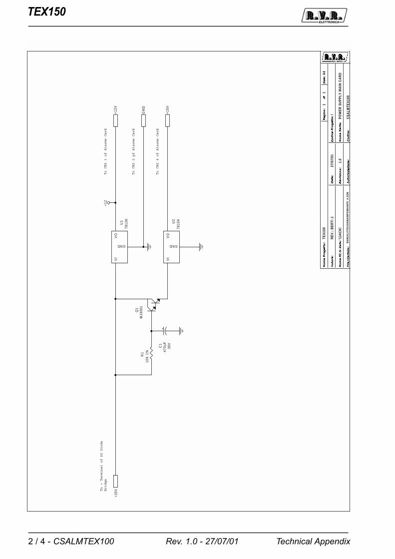
TEX150
2 / 4 - CSALMTEX100 Technical AppendixRev. 1.0 - 27/07/01
To + Terminal of D2 Diode
Bridge
To CN2 1 of Alarms Card
To CN2 4 of Alarms Card
To CN2 2 pf Alarms Card
\\JA
CK
\P
OW
ER
SU
PP
LY M
AIN
CA
RD
CS
ALM
TEX
100
1.0
TEX
150
/
MA
NU
ALI
\TEX
150\
MA
INPS
\MA
INPS
_A.D
SN
RE
V.:
BE
RTI
J.
27/0
7/01
11
A4
������������
�����
�� �����������
��������
����
�������������
����
���������
�� ���
���������
�������������
������
����
�
+12
U2
7815
K
VI
GND
VO
Q1
MJ3
001
+C
147
0uF
35V
R1
10K
1%
U1
7812
K
VI
GND
VO
+20V
+12V
+15V
GN
D

TEX150
CSALMTEX100 - 3 / 4Technical Appendix Rev. 1.0 - 27/07/01
TEX 150 Bill Of Materials Page 1
Item Quantity Reference Part DESCRIPTION PART ORDER CDE
___________________________________________________________________________________________
1 1 R1 10K 1% RESISTOR 1/4W 1% RSM1/4FK0010
2 1 C1 470UF ELECTROLYTIC CAPACITOR CEA477BM350
3 1 SW1 1V 2P DEVIATORE 1 VIA 2 POS DEV1V1103CS
4 1 U1 7812K POS. STABILIZER 1.5A CIL7812K
5 1 U2 7815K POS. STABILIZER 1.5A CIL7815K
6 1 Q1 MJ3001 POWER TRANSISTOR TRNMJ3001

TEX150
4 / 4 - CSALMTEX100 Technical AppendixRev. 1.0 - 27/07/01
Pagina lasciata intenzionalmente in biancoThis page was intentionally left blank

TEX150
CSFIN150W03 - 1 / 4Technical Appendix Rev. 1.0 - 27/07/01

TEX150
2 / 4 - CSFIN150W03 Technical AppendixRev. 1.0 - 27/07/01
RF INPUT
CAV3
RG179
CAV2
RG179
CAV1
RG179
CAV4
RG179
CAV5
RG179-25
CAV6
CAVO
CN3 7
CN3 8
to alarms card
RF OUTPUT
\\JA
CK
\S
CH
ED
A F
INA
LE T
EX
150
CS
FIN
150W
03
1.0
TEX
150
/
MA
NU
ALI
\TE
X15
0\PO
WER
_AM
P\D
ESIG
N1.
DSN
BE
RTI
J.
23/0
1/01
11
A4
No
me P
rogett
o:
Au
tore:
Co
dic
e P
rogett
o:
Nom
e P
C in
Rete
:
File/
Carte
lla:
Data
:
Revis
ion
e:
Co
dic
e:
No
me P
arte
:
Au
toriz
zazio
ne:
Pag
ina:
Siz
e:
di
+V
CC
+V
CC
+V
CC
CA
V7
SM
AF 1
2
R15
270
CH
R13
270
CH
R14
10C
H
TR
11K
CA
V5
RG
179
1
2
1
2
R2
1KC
H
CA
V4
RG
179
1
2
C15
470
pF
1
2
C19
150p
FH
Q
R5
1KC
H
C20
100p
FH
Q
D2
1N41
48
C25
470p
FH
Q
C40
470p
FH
Q
C29
1nF
C28
100u
FC
301n
FQ
4S
D14
80
Q5
SD
1480
C16
470
pF
R1
5K6
C37
1nF
C26
0.1u
F
R21
12*
C24
0.1u
F
C10
680p
FH
Q
L13
VK
L1V
K
C6
680
pFH
QC
391n
F
C22
1nF
UN
ELC
O
L5 L
59.5
RV
R1
C1
100u
F
NC
R12 10
0CH
C3
1nF
C2
1nF
L9
2m
H2
L11
2m
H2
C18
1nF
C17
470
pF
C41
470
pFH
Q
C38
1nF
R6
10#
C27
1nF
L12
2m
H2
C21
470u
F
R20
12*
C33
1nF
C32
100u
FC
341n
F
L6V
K
C23
1nF
UN
ELC
O
R16
12*
L10
L43
RV
R0.
5
Q1
TIP
120
L2
L57R
VR
1
C13
220p
F
C5
1uF
PR
41K
CH
L4L3
6.5R
VR
1
Q3
BF
Q68
R17
12*
C9
470p
F
C8
470p
F
L7 2m
H2
C11
470p
FH
Q
C12
470p
FH
Q
Q2
BLF
244
L3 VK
D3
1N41
48
C36
1nF
UN
ELC
O
C35
1nF
UN
ELC
O
D1
Z18
V
R7
10#
CA
V3
RG
1791
2C
AV
2R
G17
9
1
2
1
2
CA
V1
RG
179
1
2
C31
100p
FH
Q
1
CA
V6
CA
VO
1
R3
1KC
H
L8 L
43R
VR
0.5
C14
220
pFR
1010
#
R19
39#
C7
1nF
R18
39#
R11
270
R9
270
R8
100*
1
2 1
2
C4
1nF

TEX150
CSFIN150W03 - 3 / 4Technical Appendix Rev. 1.0 - 27/07/01
TEX 150 (150 F.M. EXCITER) Bill Of Materials Page1
Item Q.ty Reference Part Description Part Order Code______________________________________________________________________________________________
1 1 CAV1 RG179 CAVO SCHERMATO 25Ohm 23cm2 2 CAV2,CAV3 RG179 CAVO SCHERMATO 25Ohm 13cm3 2 CAV4,CAV5 RG179 CAVO SCHERMATO 25Ohm 24cm4 1 CAV6 CAVO CAVO DIA 1.5 11.5cm5 1 CAV7 SMAF CONN. SMA F TELAIO CNTSMAFPACRI7 3 C1,C28,C32 100Uf ELECTROLYTIC CAPACITOR CEA107BM3508 13 C2,C3,C4,C7,C18,C27, 1nf CERAMIC CAPACITOR CKM102BK600P
C29,C30,C33,C34,C37,C38,C39
9 1 C5 1uFT TANATALIUM CAPACITOR10 2 C6,C10 680pFHQ HIGH Q CAPACITOR ATC CHQ681AJ50011 4 C8,C9,C16,C17 470pF13 5 C11,C12,C25,C40,C41 470pFHQ HIGH Q CAPACITOR ATC CHQ471AJ50014 2 C13,C14 220pF CERAMIC CAPACITOR NP0 CKM221BK600C16 1 C15 470pF CERAMIC CAPACITOR CKM471BK600P17 1 C19 150pFHQ HIGH Q CAPACITOR ATC CHQ151AJ50018 2 C20,C31 100pFHQ HIGH Q CAPACITOR ATC CHQ101AJ50019 1 C21 470uF ELECTROLYTIC CAPACITOR CEA477BM35020 4 C22,C23,C35,C36 1nFUNELCO SILVER MICA CAPACITOR CSM102XK35121 2 C26,C24 0.1uF CERAMIC CAPACITOR CKM104BK600P24 1 D1 Z18V ZENER DIODE 18V 0.4W25 2 D2,D3 1N4148 SILICON DIODE DIS1N414826 4 L1,L3,L6,L13 VK RF CHOKE IMPVK00A27 1 L2 L57RVR1 5SP DIA7 RAME AR 1mm28 1 L4 L36.5RVR1 3SP DIA6.5 RAME AR 1mm29 1 L5 L59.5RVR1 5SP DIA9.5 RAME AR 1mm30 4 L7,L9,L11,L12 2mH2 IMPEDENZA31 2 L10,L8 L43RVR0.5 4 SP DIA3 RAME SM 0.5mm32 1 NC N.C. NON CONNESSO33 1 Q1 TIP120 NPN DARLINGTON TRNTIP12034 1 Q2 BLF244 TRANSISTOR BLF244 TRNBLF24435 1 Q3 BFQ68 NPN RF TRANSISTOR TRNBFQ6836 2 Q4,Q5 SD1480 RF POWER TRANSISTOR TRNSD148037 1 R1 5K6 RESISTOR 1/4W 5% RSC1/4JK000138 4 R2,R3,R4,R5 1KCH CHIP RESISTOR RCH085J0001K39 3 R6,R7,R10 10# RESISTOR 2W RSC002JH001040 1 R8 100* RESISTOR 1/2W 5% RSC1/2JH010041 2 R11,R9 270 RESISTOR 1/4W 5% RSC1/4JH027042 1 R12 100CH CHIP RESISTOR43 2 R15,R13 270CH CHIP RESISTOR RCH085J0270H44 1 R14 10CH CHIP RESISTOR RCH1/4JH001045 4 R16,R17,R20,R21 12* RESISTOR 1/2W 5% RSC1/2JH01246 2 R19,R18 39# RESISTOR 2W RSC002JH003947 1 TR1 1K

TEX150
4 / 4 - CSFIN150W03 Technical AppendixRev. 1.0 - 27/07/01
Pagina lasciata intenzionalmente in biancoThis page was intentionally left blank

TEX150
PSSW2812B - 1 / 4Technical Appendix Rev. 1.0 - 27/07/01

TEX150
2 / 4 - PSSW2812B Technical AppendixRev. 1.0 - 27/07/01
165KHZ
\\JA
CK
\P
OW
ER
SU
PP
LY
281
2B
PS
SW
2812
B
1.0
TE
X15
0
/
MA
NU
ALI
\TEX
150\
PSSW
2812
\PS2
812.
DSN
RE
V.:
BE
RTI
J.
01/0
9/98
11
A4
������������
�����
�� �����������
��������
����
�������������
����
���������
�� ���
���������
�������������
������
����
�
PW
R
PW
R
VR
EF
VIN
SH
DW
VIN
SH
DW
VC
C
VC
C
VC
C
R3
10
R
C3
1
CD
1KP
F/1
00
C3
0
CD
1K
PF
R5
10
R/2
W
+C1
8
CT
1/35
C1
7
CD
.1U
F
Q1IR
FZ
44
R4
4K
7R
6
10
R/2
W
C2
2
CD
1KP
F/1
00
DZ
3
15
V/1
W
R1
5
MIA
10
UH
R2
3
560K
+
C3
2
100/
25
R2
456
0K
+
C2
8
220/
35
C2
CP
.1uF
R1
01
K
+ C1
6
1000
/50
+C1
5
1000
/50
+
C1
4
1000
/50
C1
1
CP
.1uF
C3
CP
.1uF
C1
0
CP
.1uF
R2
0
47
R
D3
11
DQ
06
R1
7
47
0R
/5W
C1
9
CD
.1U
F
C4
CM
.1U
F
C8
CD
.1U
F
DZ
1
13
V/1
W
D1
11
DQ
06
+ C5
CT
1/35
+C
29
4.7u
F
R1
3
1K
C9
CP
.1uF
C6
CD
.1U
F
JP2
KR
A4
1234
R2 1K
R1
6 10K
L1
T28
12
+
C2
4
EK
R22
0/63
+C1
3
1000
/50
+C2
3
EK
R22
0/63
+C1
2
1000
/50
+C
25
EK
R22
0/63
+C
7
EK
R22
0/63
R2
1
560R
R2
6
10M
U2
UC
38
23
1 2 3 4 5 6 7 8
16 15 14 13 12 11 10 9
INV
.N
.I.
E/A
OU
TC
LK
RT
CT
RA
MP
S.S
TA
RT
VR
EF
VC
CO
UT
VC
PW
RG
ND
ILM
RE
FG
ND
ILS
.D.
R1
9N
.C.
Q2
BC
23
7
R7
3K
3
R2
21K
80
C2
1
CD
10
KP
FIS
1
4N26
12
54
6
R8
680R
C2
0
R1
22K
R1
8
10K
R1
1
4R
7
C1 4
n7
UF
2.5%
R1
4
R2
2/5
W
R9
R2
2/5
W
R1
2
5k6
JP3
ST
RIP
-2
DZ
2
3V3/
0.5
JP1
KR
A2 12
IS2
4N26
1 2
5 4
6
DZ
4
3V3/
0.5
U1
IR21
25
1 2 3 4
8 7 6 5
VC
CIN E
RR
GN
D
VB
HO
CS
VS
D2
MB
R16
60
F1
BL0
2F
2
BL0
2
C2
6C
D.1
uF
R2
782
0R
R2
8
R1
/10
W
R2
5
10
R

TEX150
PSSW2812B - 3 / 4Technical Appendix Rev. 1.0 - 27/07/01
PS2812B.SCH Bill Of Materials Page 1
Item Quantity Reference Part
____________________________________________________
1 1 C1 4n7UF
2 5 C2,C3,C9,C10,C11 CP.1uF
3 1 C4 CM.1UF
4 2 C18,C5 CT1/35
5 5 C6,C8,C17,C19,C26 CD.1UF
6 4 C7,C23,C24,C25 EKR220/63
7 5 C12,C13,C14,C15,C16 1000/50
8 1 C20 N.C.
9 1 C21 CD10KPF
10 2 C22,C31 CD1KPF/100
11 1 C28 220/35
12 1 C29 4.7uF
13 1 C30 CD1KPF
14 1 C32 100/25
15 1 DZ1 13V/1W
16 2 DZ2,DZ4 3V3/0.5
17 1 DZ3 15V/1W
18 2 D1,D3 11DQ06
19 1 D2 MBR1660
20 2 F2,F1 BL02
21 2 IS2,IS1 4N26
22 1 JP1 KRA2
23 1 JP2 KRA4
24 1 JP3 STRIP-2
25 1 L1 T2812
26 1 Q1 IRFZ44
27 1 Q2 BC237
28 1 R1 22K
29 3 R2,R10,R13 1K
30 2 R3,R25 10R
31 1 R4 4K7
32 2 R6,R5 10R/2W
33 1 R7 3K3
34 1 R8 680R
35 2 R14,R9 R22/5W
36 1 R11 4R7
37 1 R12 5k6
38 1 R15 MIA10UH
39 2 R16,R18 10K
40 1 R17 470R/5W
41 1 R19 N.C.
42 1 R20 47R
43 1 R21 560R
44 1 R22 1K80
45 2 R24,R23 560K
46 1 R26 10M
47 1 R27 820R
48 1 U1 IR2125
49 1 U2 UC3823
50 1 R28 R1/10W

TEX150
4 / 4 - PSSW2812B Technical AppendixRev. 1.0 - 27/07/01
Pagina lasciata intenzionalmente in biancoThis page was intentionally left blank

TEX150
CSAUDIOCTE - 1 / 4Technical Appendix Rev. 1.0 - 27/07/01

TEX150
2 / 4 - CSAUDIOCTE Technical AppendixRev. 1.0 - 27/07/01
1 2 3 4 5 6 7 8 9 10
EC3
GND AUDIO
GND AUDIO
GND
PWR DIR
PWR REF
VPA
VCC
VPA
GND
VCC
WIRE ON H1 H2 H5 H7 H9
NOTE:
R1 R2 OPTION FOR 600 OHM INPUT IMP.
132
4 x 0.1uF
132
REFERENCE
EC2
EC1
BNC1 -> SCA1 INPUT
BNC2 -> SCA2 INPUT
EC1 -> RIGHT (MONO) AUDIO INPUT
EC2 -> LEFT (MPX) AUDIO INPUT
EC3 -> TELEMETRY CONNECTOR
\\JA
CK
\S
CH
ED
A A
UD
IO IN
PU
T
CS
AU
DIO
CTE
1.0
TEX
150
/
MA
NU
ALI
\TEX
150\
AU
DIN
P\A
UD
IOIN
.PS
RE
V.:
BE
RTI
J.
25/0
7/01
11
A4
������������
�����
�� �����������
��������
����
�������������
����
���������
�� ���
���������
�������������
������
����
�
R1
0 0R
12 0
R1
1 0
H7
H3
H4
H2
H1
H9
H8
H6
H5
H1
0
CN
226
PIN
CO
NN
.
1 23 45 67 89 10
11 1213 1415 1617 1819 2021 2223 2425 26
R9
0
BN
C2
BN
C is
. c.
s.
BN
C1
BN
C is
. c.
s.
EC
2X
LRF
TL
EC
1X
LRF
TL
C4
33pF
L3V
K
L4V
K
L2V
K
L1V
K
C1
133
pF
C9
33pF
C1
033
pF
C5
33pF
C6
33pF
C7
33pF
C8
33pF
C1
33pF
C2
33pF
C3
33pF
EC
3M
OR
SE
TT
IER
A 1
0
123456789
10
C1
4C
16
C1
8C
20
L5V
K
L6V
K
C1
233
pF
R2
N.C
.
R1
N.C
.
CN
126
PIN
CO
NN
.
1 23 45 67 89 10
11 1213 1415 1617 1819 2021 2223 2425 26
C2
2N
.C.
C2
4N
.C.
C2
3N
.C.
C2
1N
.C.
C1
90.
1uF
C1
70.
1uF
C1
50.
1uF
C1
30.
1uF
R8
N.C
.
R7
N.C
.
R6
1K
R5
1K
R4
1K
R3
1K

TEX150
CSAUDIOCTE - 3 / 4Technical Appendix Rev. 1.0 - 27/07/01
CSAUDIOCTE Bill Of Materials Page 1
Item Quantity Reference Part Description Part Order Code
____________________________________________________________________________________________________
1 4 R3,R4, 1K RESISTOR 1/4W 5% RSC1/4JK0001
R5,R6
2 12 C1,C2,C3, 33pF CERAMIC CAPACITOR NP0 CKM330BJ600C
C4,C5,C6,
C7,C8,C9,
C10,C11,C12
3 8 C13,C14, 0.1uF CERAMIC CAPACITOR CKM104BK600P
C15,C16,
C17,C18,
C19,C20
4 6 L1,L2,L3, VK RF CHOKE IMPVK00A
L4,L5,L6
5 2 EC1,EC2 XLRFTL XLR FEMM. DA TELAIO CNTXLRFP3P
6 1 EC3 MORSET. 10 MORSETT. TEL. 10 CONT. MORSP10P
7 2 CN1,CN2 26 P CONN. CONN. M 2*13 P 2.54 CNTMCSFC26P
8 2 BNC1,BNC2 BNC IS.CS. CONN. BNC A STAMP. IS. CNTBNCFCSIS
9 10 H1,H2,H3, WIRE JUMP. PONTICELLO A FILO WIREJUMPER
H4,H5,H6,
H7,H8,
H9,H10
10 8 R1,R2,R7, N.C. RESISTOR 0OHM
R8,C21,C22,
C23,C24
11 4 R9,R10,R11, 0 NOT CONNECTED
R12

TEX150
4 / 4 - CSAUDIOCTE Technical AppendixRev. 1.0 - 27/07/01
Pagina lasciata intenzionalmente in biancoThis page was intentionally left blank

TEX150
CSSDC30A003 - 1 / 6Technical Appendix Rev. 1.0 - 27/07/01

TEX150
2 / 6 - CSSDC30A003 Technical AppendixRev. 1.0 - 27/07/01
\\JA
CK
\S
TER
EO
CO
DE
R S
DC
30A
SLS
DC
30A
002
1.0
TEX
150
/
MA
NU
ALI
\TE
X15
0\S
TER
EO
CO
DE
R\S
DC
30A
R2.
DSN
RE
V.:
BE
RTI
J.
25/0
7/01
31
A4
������������
�����
�� �����������
��������
����
�������������
����
���������
�� ���
���������
�������������
������
����
�
Inpu
t, F
iltri
e P
reen
fasi
INP
UT
.SC
H
L+ L- R+
R-
VC
C
RE
F
GN
D
RO
NL
ON
PH
LM
PX
RM
PX
LM
ON
O
RM
ON
O
LM
EA
S
RM
EA
S
Cod
er,
Sel
. F
unzi
oni
CO
DE
R.S
CH
LM
PX
RM
PX
LM
ON
O
RM
ON
O
VC
C
GN
D
CO
DE
RM
IXE
RM
ON
O
MP
X
OU
TM
EA
S
SC
A1
SC
A2
RE
F
OU
T
SC
A1
RO
N
SC
A2
LO
N
L+M
PX
MIX
ER
L-O
UT
R+
R-
+VL
M+V
MM
LO
N
RE
FR
MR
EF
GN
DG
ND
RO
NC
OD
ER
LO
NM
IXE
RP
HP
HM
ON
O
RO
N
+V+V
MO
NO
AU
_A
LC
OD
ER
RE
F
+V
L++V
L- L+
SC
A1
SC
A2
R+
L-R
-O
UT
MM
MP
XL+
R+
R-
R+
x1x3
x1x3
MM
x2x4
x2x4
LM
RM
GN
D
+V
AU
_A
L
C5
20.
1uF
JP1
CN
26
PD
OU
TP
UT
12
34
56
78
910
1112
1314
1516
1718
1920
2122
2324
2526
JP2
CN
26
PD
INP
UT
12
34
56
78
910
1112
1314
1516
1718
1920
2122
2324
2526
JP3
CN
10
PD
ME
AS
UR
E
12
34
56
78
910
SW
1A
SW
WP
4_2
CO
DE
R
21 3
SW
2A
NC
LEF
T
21 3
SW
3A
NC
PH
AS
E
21 3
SW
4A
NC
RIG
HT
21 3
SW
5A
SW
WP
4_2
MO
NO
21 3
D1
LED
-G5
R1
1K8
D2
NC
R2
NC
D3
NC
JP16
ST
M03
S60
0H
1 2 3
R3
NC
D4
NC
R4
NC
D5
LED
-G5
R5
1K8
R11
760
4H0
R11
860
4H0
JP17
ST
M03
S60
0H
1 2 3
+C
53
100u
FR
126
10K
0
R12
510
K0
D1
0
1N41
48 D1
11N
4148
D1
2
1N41
48
D1
3
1N41
48
JP18
JSM
03L-
R
1 2 3
FIX
5F
IX35
FIX
6F
IX35
+ -
U1
1A
LM39
33 2
1
48
R11
639
K0
R11
58K
20
R8
147
0K0
R8
210
K0
Q5
PB
C5
57 J6
JSM
DL
OA
D
C3
7
0.1u
F
J7JS
MD
CM
EA
S
12
R10
5
10K
0
+ -
U1
1B
LM39
35 6
7
R11
3
10K
0
+C
36
2.2u
F
TP
18
TP
GN
D
D8
1N41
48
+C
48
47uF
R10
42M
20
R10
3
56K
0
R10
13K
30R10
2
100K
0R
114
1K0
TP
17
TP
AU
AL
OU
T
FIX
1F
IX35
FIX
2F
IX35
FIX
3F
IX35
FIX
4F
IX35

TEX150
CSSDC30A003 - 3 / 6Technical Appendix Rev. 1.0 - 27/07/01
J1, J2, J3 e J4 vanno fatti lato componenti
SW6, RV2, RV3 VANNO MONTATI LATO SALDATURE
470uF
\\JA
CK
\IN
PU
T,FI
LTE
R,P
RE
EM
PH
AS
YS
SLS
DC
30A
0002
1.0
TEX
150
/
MA
NU
ALI
\TE
X15
0\S
TER
EO
CO
DER
\SD
C30
AR
2.D
SN
RE
V.:
BE
RTI
J.
25/0
7/01
32
A3
������������
�����
�� �����������
��������
����
�������������
����
���������
�� ���
���������
�������������
������
����
�
+V
ref
ref
ref
ref
ref
LO
N
PH
ref
ref
ref
ref
R-
ref
LMP
XR
MO
NO
RM
PX
RO
NR
ON
PH
ref
ref
+V ref
LO
N
L+ L- R+
LMP
X
LMP
X
RM
PX
RM
PX
+V
GN
D
+V
+V
+V
+V
+V
+V
LM
ON
O
VD
D
VE
E
VS
S
R29
2K49
J1 J3
cw
RV
220
K
R-V
AR
R27
7K15
R26
10K
0
R28
4K99
+ -
U3B
TL0
725 6
7R
24
4K99
R25
14K
0
R30
1K78
J21
2
HY
1IR
V30
FT
12345678910 11
121314151617181920INA
GNDGND
-VGNDGND
OUTAGNDGND
+V INBGNDGND-VGNDGNDOUTBGNDGND+V
R12
7
1M0
R12
8
1M0
R34
10K
0
+ -
U2A
TL0
723 2
1
48
C50
22pF
J41
2
+
C6
100u
F
+
C7
100u
F
R14
4K99
+
C8
100u
F
R13
14K
7
R15
4K99
R16
14K
7
+
C9
100u
F
R10
4K99
R11
4K99
R12
14K
7
+ -
U2B
TL0
72
5 67
R57
39K
0
R33
10K
0
+C25
10uF
R9
14K
7
R55
8K20
R31
10K
0R
32
10K
0
R56
39K
0
+C
2710
uF
+ -
U5B
TL0
72
5 67
1 0U4A
4053 11
6
14
1213
R54
8K20
R40
10K
0
R41
4K99
R42
4K99
+C26
10uF
1 0U4
C40
53 9
4
53R
37
10K
0R
38
10K
0
R39
10K
0
R35
P
82K
5
R36
82K
5
+ -
U6B
TL0
725 6
7
1 0U4B
405310
15
1 2
TP
4TPLE
FT
2
TP
3TPR
IGH
T2
cwR
V1
1K38K
NU
LL
R12
9
10K
0
R22
2K49
C51
22pF
TP
1TPLE
FT
1
TP
2TPR
IGH
T1
R23
1K78
cw
RV
320
K
L-V
AR
R20
7K15
R21
4K99
+ -
U3A
TL0
723 2
1
48
R17
4K99
R18
14K
0R
1910
K0
C19
100p
F
R46
680H
0
cw
SW
6B
SW
59
40
P
8910121314
11
cw
SW
6A
SW
59
40
P
123567
4
+ -
U6A
TL0
723 2
1
48
R45
22K
1
C17
1nF
C18
2n2
C21
0.1u
F
C14
1nF
C15
2n2
C16
100p
F
JP4
ST
M03
SR
-50u
S
1 2 3JP7
ST
M03
SL-
50uS
1 2 3
JP6
ST
M03
SL-
25uS1 2 3
JP5
ST
M03
SR
-25u
S
1 2 3
+ -
U7A
LM39
3
3 21
48
+C
222.
2uF
+
C54
47uF
C20
0.1u
F
R48
4K99
C23
0.1u
F
R12
3
10H
0
R12
210
H0
Q4
BC
557
R50
4K99
R47
470K
0
Q3
BC
557
C13
0.1u
F
+ -
U7B
LM39
35 6
7
+C
242.
2uF
R49
470K
0
R44
680H
0
C10
0.1u
F
C11
0.1u
F
C12
0.1u
F
R52
10K
0
R43
22K
1
R51
10K
0R
5310
K0
+ -
U5A
TL0
723 2
1
48
L+ L- R+ R-
VC
C
GN
D
LMP
X
RM
PX
RM
ON
O
RO
N
LO
N
PH
RE
FLM
EA
SR
ME
AS
LM
ON
O

TEX150
4 / 6 - CSSDC30A003 Technical AppendixRev. 1.0 - 27/07/01
Il CODER va montato lato saldature evitando componenti sul bordo
J5, J6 e J7 vanno fatti lato componenti
470uF
\\JA
CK
\S
TER
EO
CO
DE
R,F
UN
CTI
ON
SEL
ECTO
R,C
LIPP
ER
SLS
DC
30A
0002
1.0
TEX
150
/
MA
NU
ALI
\TE
X15
0\S
TER
EO
CO
DER
\SD
C30
AR
2.D
SN
RE
V.:
BE
RTI
J.
25/0
7/01
33
A3
������������
�����
�� �����������
��������
����
�������������
����
���������
�� ���
���������
�������������
������
����
�
ref
ref
CL+
CL-
ref
CLI
PP
LM
ON
O+V
ref
ref
CL+
pil
MP
XC
OD
mon
oon
CL-
mix
er
ref
pil
MP
XC
OD
RM
ON
O
code
rm
ixer
LM
ON
O
LM
ON
OC
LIP
Pre
f+V
ref
ref
ref
OU
T
mon
o
pil
code
r
mix
er
mon
o
ref
ref
RM
ON
O
RM
ON
O
+V
+V
+V
+V
GN
D
+V
+V
+V
+V
VD
D
VE
E
VS
S
R8
1K0
Q1
BC
547
R10
910
0K0
R10
810
K0
R10
710
K0
+C
4710
uF
TP
15
TP 19K
TT
LD
94V
7
R11
2
2K20
C49
0.1u
F
cw
RV
850
KS
EP
-LC
OD
1
IRV
30C
T
14 13 12 11 10 9 8 7 6 5 4 3 2 127262524232221201918171615
R-O
UT
R-I
NG
ND
VE
EG
ND
L-IN
L-O
UT
GN
DG
ND
TP
119
K-O
UT
GN
DP
IL-A
DJ
ST
-ON
PH
AS
E-A
DJ
PIL
-OU
TV
CC
MP
XC
INT
GN
DG
NDCL
CR
SE
P-R
SE
P-L
PIL
-IN
MP
U
JP15
ST
M03
S19
KT
TL1
23
TP
16
TP GN
D
cw
RV
710
KP
IL-L
EV
C41
CV
40pF
PIL
-PH
C42
CV
20pF
PIL
-FQ
cw
RV
650
KS
EP
-R
U9
4053
12 13 2 1 5 3 6 11 10 9
14 15 4
X0
X1
Y0
Y1
Z0
Z1
INH A B C
X Y Z
R58
14K
0U
8
4053
12 13 2 1 5 3 6 11 10 9
14 15 4
X0
X1
Y0
Y1
Z0
Z1
INH A B C
X Y Z
C28
0.1u
F
JP9
ST
M03
SL-
SE
L123
JP8
ST
M03
SR
-SE
L
123
R61
10K
0
R59
4K99
C29
0.1u
F
R64
10K
0
R63
10K
0
+ -
U10
AT
L072
3 21
48
R60
4K99
R62
10K
0
TP
9TP LE
FT
3
TP
5
TP 4864
K
TP
7TPM
PX
2
R65
4K99
TP
6TPM
PX
1
TP
8TPR
IGH
T3
R69
49K
9
R67
49K
9
JP10
ST
M03
S
CLI
PP
ER
123
+ -
U10
B
TL0
72
5 67
R68
49K
9
R70
124K
0
R71
10K
0
+ -
U13
AT
L072
3 21
48
R73
10K
0
+ -
U13
BT
L072
5 67
R72
10K
0
R66
10K
0
R76
47K
0
+C30
220u
F
R75
10K
0
R74
4K99
TP
11
TPMP
X0
R77
10K
0
+C31
100u
F
TP
10
TP MP
X3
C34
10nF
C33
10nF
TP
12TP G
ND
C32
0.1u
F
JP12
ST
M03
SS
CA
2SE
L
123T
P14
TP GN
D
TP
13
TP SC
A3
C35
10nF
JP11
ST
M03
SS
CA
1LE
V
123
R80
22K
0
R79
22K
0
R78
22K
0
R85
10K
0R
8410
K0
R83
10K
0
JP13
ST
M03
SP
ILO
T
1 2 3
R86
10K
0D
7
1N41
48
D6
1N41
48
J5
R89
4K42
Q6
BC
547
R88
10K
0
R87
10K
0
R90
4K99
R10
6
1K0
cw RV
55K
CL-
LEV
cwRV
41K
CL-
SY
M
R92
10K
0
R91
10K
0
+ -
U14
BLM
358N
5 67
+ -
U14
ALM
358N
3 21
48
U12
EC
A30
96
141513
C38
0.1u
F
R94
10K
0
R93
10K
0
U12
BC
A30
96
56 4
R12
0
10H
0U12
AC
A30
96
13 2
16
R11
9
10H
0
R96
47K
0
R95
47K
0
U12
CC
A30
968
9 7
U12
DC
A30
96
111210
C39
47pF
R98
2K20
R97
10K
0
Q7
BC
557
C43
0.1u
F
C40
47pF
R10
02K
20
R99
10K
0
+ -
U1B
TL0
72
5 67
+C
4610
uF
+C
4510
uF
C44
0.1u
F
+ C1
10uF
R7
10K
0
R6
10K
0
+ -
U1A
TL0
723 2
1
48
+C4
47uF
+C
347
uF
C5
0.1u
F
C2
0.1u
F
LM
ON
O
RM
ON
O
MP
X
SC
A1
SC
A2
CO
DE
R
MIX
ER
MO
NO
LMP
X
RM
PX
VC
C
GN
D
RE
F
OU
T

TEX150
CSSDC30A003 - 5 / 6Technical Appendix Rev. 1.0 - 27/07/01
SLSDC30A002 Bill Of Materials Page1
ItemQuantity Reference Part
_______________________________________________________________________________________________
1 1 COD1 IRV30CT
2 7 C1,C25,C26,C27,C45,C46, 10uF
C47
3 18 C2,C5,C10,C11,C12,C13, 0.1uF
C20,C21,C23,C28,C29,C32,
C37,C38,C43,C44,C49,C52
4 4 C3,C4,C48,C54 47uF
5 6 C6,C7,C8,C9,C31,C53 100uF
6 2 C17,C14 1nF
7 2 C18,C15 2n2
8 2 C19,C16 100pF
9 3 C22,C24,C36 2.2uF
10 1 C30 220uF
11 3 C33,C34,C35 10nF
12 2 C39,C40 47pF
13 1 C41 CV40pF
14 1 C42 CV20pF
15 2 C50,C51 22pF
16 2 D1,D5 LED-G5
17 9 SW2,R2,D2,SW3,R3,D3,SW4, NC
R4,D4
18 7 D6,D7,D8,D10,D11,D12,D13 1N4148
19 1 D9 4V7
20 6 FIX1,FIX2,FIX3,FIX4,FIX5, FIX35
FIX6
21 1 HY1 IRV30FT
22 2 JP1,JP2 CN26PD
23 1 JP3 CN10PD
24 13 JP4,JP5,JP6,JP7,JP8,JP9, STM03S
JP10,JP11,JP12,JP13,JP15,
JP16,JP17
25 1 JP18 JSM03
26 4 J1,J3,J5,J6 JSMD
27 3 J2,J4,J7 JSMDC
28 2 Q1,Q6 BC547
29 4 Q3,Q4,Q5P,Q7 BC557
30 2 RV4,RV1 1K
31 2 RV2,RV3 20K
32 1 RV5 5K
33 2 RV8,RV6 50K
34 1 RV7 10K
35 2 R1,R5 1K8
36 45 R6,R7,R19,R26,R31,R32, 10K0
R33,R34,R37,R38,R39,R40,
R51,R52,R53,R61,R62,R63,
R64,R66,R71,R72,R73,R75,
R77,R82,R83,R84,R85,R86,
R87,R88,R91,R92,R93,R94,
R97,R99,R105,R107,R108,
R113,R125,R126,R129
37 3 R8,R106,R114 1K0
38 4 R9,R12,R13,R16 14K7
39 17 R10,R11,R14,R15,R17,R21, 4K99
R24,R28,R41,R42,R48,R50,
R59,R60,R65,R74,R90

TEX150
6 / 6 - CSSDC30A003 Technical AppendixRev. 1.0 - 27/07/01
40 3 R18,R25,R58 14K0
41 2 R27,R20 7K15
42 2 R29,R22 2K49
43 2 R30,R23 1K78
44 2 R35P,R36 82K5
45 2 R45,R43 22K1
46 2 R46,R44 680H0
47 3 R47,R49,R81 470K0
48 3 R54,R55,R115 8K20
49 3 R56,R57,R116 39K0
50 3 R67,R68,R69 49K9
51 1 R70 124K0
52 3 R76,R95,R96 47K0
53 3 R78,R79,R80 22K0
54 1 R89 4K42
55 3 R98,R100,R112 2K20
56 1 R101 3K30
57 2 R102,R109 100K0
58 1 R103 56K0
59 1 R104 2M20
60 2 R117,R118 604H0
61 4 R119,R120,R122,R123 10H0
62 2 R127,R128 1M0
63 2 SW1,SW5 SWWP4_2
64 1 SW6 SW5940P
65 18 TP1,TP2,TP3,TP4,TP5,TP6, TP
TP7,TP8,TP9,TP10,TP11,
TP12,TP13,TP14,TP15,TP16,
TP17,TP18
66 7 U1,U2,U3,U5,U6,U10,U13 TL072
67 3 U4,U8,U9 4053
68 2 U11,U7 LM393
69 1 U12 CA3096
70 1 U14 LM358N

TEX150
CSAFM-MPX002 - 1 / 4Technical Appendix Rev. 1.0 - 27/07/01

TEX150
2 / 4 - CSAFM-MPX002 Technical AppendixRev. 1.0 - 27/07/01

TEX150
CSAFM-MPX002 - 3 / 4Technical Appendix Rev. 1.0 - 27/07/01
SLAFM-MPX002 Bill Of Materials Page 1
Item Q.ty Reference Part
_____________________________________________________________________________________________________
1 11 C1,C16,C18,C21,C23,C24, 0.1uF
C25,C26,C27,C28,C29
2 3 C2,C19,C34 220uF
3 6 C3,C4,C5,C6,C32,C33 100uF
4 2 C7,C8 10nF
5 1 C9 1nF
6 1 C10 100pF
7 1 C11 2n2
8 3 C12,C13,C14 2.2uF
9 3 C15,C17,C20 10uF
10 1 C22 47uF
11 2 C30,C31 47pF
12 1 D1 1N4148
13 4 FIX1,FIX2,FIX3,FIX4 FIX35
14 2 JP1,JP5 CN26PD
15 2 JP2,JP3 STM04S
16 5 JP4,JP7,JP8,JP9,JP10 STM03S
17 1 JP6 CN10PD
18 1 J1 JSMD
19 1 J2 JSMDC
20 2 LPF1,LPF2 LPF19K1
21 4 Q1,Q2,Q3,Q4 BC557
22 1 Q5 BC547
23 2 RV1,RV2 20K
24 2 RV3,RV5 1K
25 1 RV4 5K
26 2 R1,R16 604H0
27 6 R2,R5,R8,R17,R20,R23 14K7
28 8 R3,R4,R6,R11,R18,R19,R21, 5K11
R26
29 2 R7,R22 1M0
30 19 R9,R14,R24,R29,R31,R32, 10K0
R47,R51,R55,R56,R57,R58,
R59,R63,R64,R65,R67,R76,
R78
31 2 R10,R25 7K15
32 5 R12,R15,R27,R30,R42 2K49
33 2 R13,R28 1K78
34 2 R33,R34 24K9
35 1 R35 88K7
36 1 R36 750
37 1 R37 21K5
38 1 R38 33K0
39 1 R39 7K50
40 1 R40 4K64
41 1 R41 5K90
42 4 R43,R61,R73,R74 4K99
43 3 R44,R48,R52 39K0
44 3 R45,R49,R53 8K20
45 3 R46,R50,R54 470K0
46 3 R60,R66,R68 1K0
47 1 R62 10H0
48 1 R69 221H0

TEX150
4 / 4 - CSAFM-MPX002 Technical AppendixRev. 1.0 - 27/07/01
49 1 R70 7K87
50 1 R71 56K2
51 1 R72 2M21
52 1 R75 4K42
53 2 R77,R79 2K21
54 2 R81,R80 47K5
55 1 SW1 SW5940P
56 6 TP1,TP2,TP3,TP4,TP5,TP6 TP15
57 2 U2,U1 LM393
58 4 U3,U4,U5,U6 TL072
59 2 U8,U7 LM358N
60 1 U9 CA3096

TEX150
CSSINTEX100 - 1 / 4Technical Appendix Rev. 1.0 - 27/07/01

TEX150
2 / 4 - CSSINTEX100 Technical AppendixRev. 1.0 - 27/07/01
16
6
25
To Pin 5 JP1
KHz x 1
7
521
MHz x 1
17
16
KHz x 10
23
KHz x 100
11
24
10
14
18
TCXO Card
12
9
to sp8680
EXT.REFER.1KHz
8
14
7
8
19
To Pin 1 JP1
3
TCXO Card
4
20
7
22
MHz x 10
\\JA
CK
\P
LL C
IRC
UIT
DIA
GR
AM
CS
SIN
TEX
100
1.0
TEX
150
/
MAN
UALI
\TEX
150\
PLL\
PLL_
A.DS
N
RE
V.:
BE
RTI
J.
25/0
7/01
11
A3
������������
�����
�� �����������
��������
����
�������������
����
���������
�� ���
���������
�������������
������
����
�
8
16
16
8
1616
8
8
8
16
16
8
16
+15
F
+15
V
8
+15
V
J1
+15
V
+15
V
+5V
J6
+5V
+15
V
J4
+15
V
+5V
J5 SM
B
J2 SM
B
J72
PIN
ST
RIP
R49
0
R39
22 1
%
R47
100
1%
R46
N.C
.
CN
1
DB
25 M
F
13251224112310229218207196185174163152141
R41
56 1
%
C37
4n7
R42
47 1
%R
4310
1%
C38
220p
F
C36
2p2
C40
4n7
R44
220
1%
C42
0.1u
FC
39N
.C.
R45
22K
1%
Q4
BF
R96
C41
4n7
C35
330p
F
L4 2u2
U3
4046
3 4 14 6 7 5 11 12
1 2 13 9 10 15
CIN
VC
OU
T
SIN
CX
CX
INH
R1
R2
PP P1
P2
VC
OIN
DE
MO
ZE
N
+C
1610
uF 50V
C11
47nF
+C
1210
uF50
V
+C
1410
uF 50V
C3
47nF
+C
2347
uF50
V
C28
0.1u
F+
C30
10uF
50V
+C
3210
uF 50V
R36
1K5
1%
C29
0.1u
F
U1A
4520
1 2 7
3 4 5 6
CLK
EN
RS
T
Q0
Q1
Q2
Q3
U1B
4520
91015
11121314
CLKE
N
RS
T
Q0
Q1
Q2
Q3
C31
0.1u
FC
330.
1uF
C27
0.1u
F
R34
270
1%+
C25
10uF
50V
U7C
7400
9108
U7B
7400
4 56
+C
2410
uF50
V
R33
470
1%
U13
74LS
190
153
12
106
9713
14451112
AQ
AB
QB
CQ
CD
QD
RC
OC
LKGD
/UL
OA
DMX
/MN
U5
74LS
196
45
109
32
1112
8 6 1 13
AQ
AB
QB
CQ
CD
QD
CLK
1C
LK2
LO
AD
CLR
U11
74LS
190
153
12
106
9713
14451112
AQ
AB
QB
CQ
CD
QD
RC
OC
LKGD
/UL
OA
DMX
/MN
R35
180
U9
74LS
190
153
12
106
9713
14451112
AQ
AB
QB
CQ
CD
QD
RC
OC
LKGD
/UL
OA
DMX
/MN
R40
470
1%
U10
74LS
190
153
12
106
9713
14451112
AQ
AB
QB
CQ
CD
QD
RC
OC
LKGD
/UL
OA
DMX
/MN
C43
10uF
50V
U7A
7400
1 23
U12
74LS
190
153
12
106
9713
14451112
AQ
AB
QB
CQ
CD
QD
RC
OC
LKGD
/UL
OA
DMX
/MN
R22
27 1
%
R38
1K 1
%
R18
1K 1
%R
1682
K 1
%
+
C18
22uF
50V
R9
10K
1%
R19
47K
1%
R20
1K 1
%
R30
1K 1
%
R26
1K 1
%
+C
2210
uF50
V
R28
27K
1%
R14
10K
1%
R17
1K 1
%
+C
1510
uF 50V
U2B
4518
9 10 15
11 12 13 14
CLK
EN
RS
T
Q0
Q1
Q2
Q3
R8
100
1%
R7
5K6
1%
R5
100
1%
R10
22K
1%
R4
470
1%
Q2
2N91
8
D3
1N41
48
R6
100
1%
R3
390
1%
U2A
4518
1 2 7
3 4 5 6
CLK
EN
RS
T
Q0
Q1
Q2
Q3
C9
47nF
D2
1N41
48
+C
1010
uF50
V
C21
0.1u
F
R48
33K
1%
C6
560p
F
C19
0.1u
FT
Q3
BC
547
R29
1M 1
%
R25
47K
1%
R27
1K 1
%
R37
1K5
1%
R21
470
1%
R32
270
1%
R12
10K
1%
C26
0.1u
F
R13
1K5
1%
R23
100K
1%
R11
4K7
1%
+
C20
100u
F50
V
R31
2K2
1%
+C
1722
uFT
16V
110
L2 VK
15
L122
0uH
+C
710
uF50
V
+C
810
uF50
V
L3 VK
18
14
15
14
RR
1
18
12
RR
21
2
RR
2K2
RR
2
19
RR
2K2
16
13
RR
2K2
RR
1
17
13
RR
2
17
RR
2K2
19
RR
2K2
RR
1
16
RR
2K2
110
C34
1n5P
U6
7805
1
2
3
+
C13
2.2u
FT
20V
+ -U
4AT
L082
3 21
8 4
+ -
U4B
TL0
82
5 67
R24
10M
1%
JP1
4 P
IN S
TR
IP
12
34
56
78
R15
39K
1%
U8
SP
8680
1
2
3
4
5
6
7
8 9
10
11
12
13
14
15
16
RF
RF

TEX150
CSSINTEX100 - 3 / 4Technical Appendix Rev. 1.0 - 27/07/01
CSSINTEX100 Bill Of Materials Page 1
Item Quantity Reference Part DESCRIPTION PART ORDER CODE
________________________________________________________________________________________________
1 1 R49 0 0 OHM RESISTOR R000
2 1 R43 10 1% RESISTOR 1/4W 1% RSM1/4FH0010
3 1 R39 22 1% RESISTOR 1/4W 1% RSM1/4FH0022
4 1 R22 27 1% RESISTOR 1/4W 1% RSM1/4FH0027
5 1 R42 47 1% RESISTOR 1/4W 1% RSM1/4FH0047
6 1 R50 47# RESISTOR 2W RSC002JH0047
7 1 R41 56 1% RESISTOR 1/4W 1% RSM1/4FH0056
8 4 R5,R6,R8,R47 100 1% RESISTOR 1/4W 1% RSM1/4FH0100
9 1 R35 180 RESISTOR 1/4W 5% RSC1/4JH0180
10 1 R44 220 1% RESISTOR 1/4W 1% RSM1/4FH0220
11 2 R32,R34 270 1% RESISTOR 1/4W 1% RSM1/4FH0270
12 1 R3 390 1% RESISTOR 1/4W 1% RSM1/4FH0390
13 4 R4,R21,R33,R40 470 1% RESISTOR 1/4W 1% RSM1/4FH0470
14 1 R2 820 1% RESISTOR 1/4W 1% RSM1/4FH0820
15 7 R17,R18,R20,R26,R27,R30, 1K 1% RESISTOR 1/4W 1% RSM1/4FK0001
R38
16 3 R13,R36,R37 1K5 1% RESISTOR 1/4W 1% RSC1/4FK01,5
17 1 R31 2K2 1% RESISTOR 1/4W 1% RSC1/4FK02,2
18 1 R11 4K7 1% RESISTOR 1/4W 1% RSM1/4FK04,7
19 1 R7 5K6 1% RESISTOR 1/4W 1% RSM1/4FK05,6
20 3 R9,R12,R14 10K 1% RESISTOR 1/4W 1% RSM1/4FK0010
21 2 R10,R45 22K 1% RESISTOR 1/4W 1% RSM1/4FK0022
22 1 R28 27K 1% RESISTOR 1/4W 1% RSM1/4FK0027
23 1 R48 33K 1% RESISTOR 1/4W 1% RSM1/4FK0033
24 1 R15 39K 1% RESISTOR 1/4W 1% RSM1/4FK0039
25 2 R19,R25 47K 1% RESISTOR 1/4W 1% RSM1/4FK0047
26 1 R16 82K 1% RESISTOR 1/4W 1% RSM1/4FK0082
27 1 R23 100K 1% RESISTOR 1/4W 1% RSM1/4FH0100
28 2 R1,R29 1M 1% RESISTOR 1/4W 1% RSM1/4FM0001
29 1 R24 10M 1% RESISTOR 1/4W 1% RSM1/4FM0010
30 2 RR1,RR2 RR2K2 RESISTOR NETWORK RRR1/4JK02,2
31 1 C36 2P2 CERAMIC CAPACITOR NP0 CKM2,2BJ600C
32 1 C2 M10PF PRECISION TRIMMER CAP. CVA100BK101
33 1 C1 18PF CERAMIC CAPACITOR NP0 CKM180BJ600C
34 1 C5 33PF CERAMIC CAPACITOR NP0 CKM330BJ600C
35 1 C38 220PF CERAMIC CAPACITOR NP0 CKM221BK600C
36 1 C35 330PF CERAMIC CAPACITOR CKM331BK600P
37 1 C6 560PF CERAMIC CAPACITOR CKM561BK600P
38 1 C34 1N5P POLIESTER CAPACITOR CPE152BK101
39 3 C37,C40,C41 4N7 CERAMIC CAPACITOR CKM472BK600P
40 4 C3,C4,C9,C11 47NF CERAMIC CAPACITOR CKM473BK600P
41 8 C21,C26,C27,C28,C29,C31, 0.1UF CERAMIC CAPACITOR CKM104BK600P
C33,C42
42 1 C19 0.1UFT TANTALIUM CAPACITOR CET104AM350
43 1 C13 2.2UFT TANTALIUM CAPACITOR CET225AM350
44 13 C7,C8,C10,C12,C14,C15, 10UF ELECTROLYTIC CAPACITOR CEA106AM350
C16,C22,C24,C25,C30,C32,
C43
45 1 C18 22UF ELECTROLYTIC CAPACITOR CEA226BM350
46 1 C17 22UFT TANTALIUM CAPACITOR CET226AM350
47 1 C23 47UF ELECTROLYTIC CAPACITOR CEA476BM630
48 1 C20 100UF ELECTROLYTIC CAPACITOR CEA107BM350
49 1 L4 2U2 RF CHOKE IMP02U2A
50 1 L1 220UH RF CHOKE IMP220UA
51 2 L2,L3 VK RF CHOKE IMPVK00A

TEX150
4 / 4 - CSSINTEX100 Technical AppendixRev. 1.0 - 27/07/01
Pagina lasciata intenzionalmente in biancoThis page was intentionally left blank
52 1 J7 2 PIN STRIP STRIP M P 2.54 2 PIN CNTSTRIPMCS
53 1 JP1 4 PIN STRIP STRIP M P 2.54 4 PIN CNTSTRIPMCS
54 1 J1 2 PIN JUMP MINIJUMPER P 2.54 MINIJUMPER
55 1 CN1 DB25 M F CONN. M 25 FILTRATO MURATA
56 2 J2,J5 SMB CONN. SMB A CRIMP. RG188 CNTSMBFCVD
57 1 XTAL TERM1 PTH CRYSTAL HEATER PTHHC18
58 1 X1 Q4MHZ CRYSTAL QRZ4HC18
59 3 D1,D2,D3 1N4148 SILICON DIODE DIS1N4148
60 1 U6 7805 POS. STABILIZER 1A CIL7805P
61 1 Q3 BC547 NPN TRANSISTOR TRNBC547
62 1 Q2 2N918 NPN RF TRANSISTOR TRN2N918
63 1 Q4 BFR96 NPN RF TRANSISTOR TRNBFR96
64 1 Q1 BF245B FET TRANSISTOR TRNBF245B
65 1 U4 TL082 DOUBLE OP. AMP. CILTL082
66 1 U8 SP8680 ECL DIVIDER CIDSP8680B
67 1 U3 4046 CMOS PHASE COMPARATOR CID4046
68 1 U2 4518 CMOS BCD DIVIDER CID4518
69 1 U1 4520 CMOS BIN DIVIDER CID4520
70 1 U7 7400 TTL QUAD NAND CID7400
71 5 U9,U10,U11,U12,U13 74LS190 TTL BCD DIVIDER CID74LS190
72 1 U5 74LS196 TTL LS DIVIDER CID74LS196
73 2 C39,R46 N.C. NOT CONNECTED

TEX150
CSTCXO02 - 1 / 4Technical Appendix Rev. 1.0 - 27/07/01

TEX150
2 / 4 - CSTCXO02 Technical AppendixRev. 1.0 - 27/07/01
F Out
10MHz
4MHz
2MHz
1MHz
500KHz
100KHz
J1
J2
J3
J4
J5
J6
J7
J8
XX
XX
XX
XX
XX
XX
XX
XX
\\JA
CK
\S
CH
ED
A T
CX
O
CS
TCX
O02
1.0
TEX
150
/
MA
NU
ALI
\TEX
150\
PLL\
TCXO
1.D
SN
RE
V.:
BE
RTI
J.
25/0
7/01
11
A4
������������
�����
�� �����������
��������
����
�������������
����
���������
�� ���
���������
�������������
������
����
�
5V
5VG
ND
VC
C
GN
D
JP1
ST
M06
SO
123456
R2
270
R1
4K7
C1
0.1u
FJ3
C2
0.1u
FR
315
0K
D
Q1
MM
BF
J310
J6
J1
J2
U1A
74H
C39
0SM
D
1 4 2
3 5 6 7
CK
AC
KB
CL
R
QA
QB
QC
QD
J8J7R
447
0
Q2
BC
857
J5
U1B
74H
C39
0SM
D
15 12 14
13 11 10 9
CK
AC
KB
CL
R
QA
QB
QC
QD
J4
TC
X1
TC
XO
S
123 4
OU
T
VC
CG
ND
GN
D
FIX
1F
IX35

TEX150
CSTCXO02 - 3 / 4Technical Appendix Rev. 1.0 - 27/07/01
TCXO10MHZ Bill Of Materials Page 1
Item Quantity Reference Part
__________________________________________________
1 2 C1,C2 0.1uF
2 1 FIX1 FIX35
3 1 JP1 STM06SO
4 8 J1,J2,J3,J4,J5,J6,J7,J8 JSMD
5 1 Q1 MMBFJ310
6 1 Q2 BC857
7 1 R1 4K7
8 1 R2 270
9 1 R3 150K
10 1 R4 470
11 1 TCX1 TCXOS
12 1 U1 HC390SMD

TEX150
4 / 4 - CSTCXO02 Technical AppendixRev. 1.0 - 27/07/01
Pagina lasciata intenzionalmente in biancoThis page was intentionally left blank

TEX150
SLWSTDTEX100 - 1 / 4Technical Appendix Rev. 1.0 - 27/07/01

TEX150
2 / 4 - SLWSTDTEX100 Technical AppendixRev. 1.0 - 27/07/01
R.F. OUTPUT CONNECTOR
REF PWR
FWD PWR
E F
R.F. TEST -40dB
INPUT R.F.FROM LOW PASS
FILTER
TO METER CARD
\\JA
CK
\D
IRE
CTI
ON
AL
CO
UP
LER
WS
TD1
1.0
TEX
150
/
MA
NU
ALI
\TEX
150\
DIR
CPL
\DIR
CO
UP.
DSN
RE
V.:
BE
RTI
J.
25/0
7/01
11
A4
������������
�����
�� �����������
��������
����
�������������
����
���������
�� ���
���������
�������������
������
����
�
CF
31n
FP
AS
C6
2p2
CF
41n
FP
AS
R12
47.5
1%
R13
47.5
1%
R6
10K
1%
R9
10K
1%
R14
47 1
%
CN
2B
NC
TE
LAIO
CN
1N
CO
NN
EC
TO
R
R2
47#
R1
47#
R8
10K
1%
R5
10K
1%
D1
1N41
48
TR
1W
IDE
-BA
ND
TR
F
R3
1K*
C2
T2p
22F
D2
1N41
48

TEX150
SLWSTDTEX100 - 3 / 4Technical Appendix Rev. 1.0 - 27/07/01
WSTD1 Bill Of Materials Page 1
Item Quantity Reference Part DESCRIPTION PART CODE
__________________________________________________________________________________________________
1 1 R14 47 1% RESISTOR 1/4W 1% RSM1/4FH0047
2 2 R1,R2 47# RESISTOR 2W RSC002JH0047
3 2 R12,R13 47.5 1% RESISTOR 1/4W 1% RSM1/4FH47.5
4 1 R3 1K* RESISTOR 1/2W 5% RSC1/2JK0001
5 4 R5,R6,R8,R9 10K 1% RESISTOR 1/4W 1% RSM1/4FK0010
6 1 C6 2P2 CERAMIC CAPACITOR NP0 CKM2,2BJ600C
7 1 C2 T2P22F TRIMMER CAPACITOR CVC2,22CK600
8 2 C3,C4 1NFPAS CERAMIC THROUGH CAPACITOR CDP102XK500
9 1 CN2 BNC TELAIO CONN. BNC A TELAIO CNTBNCFPV
10 1 CN1 N CONNECTOR CONN. N A TELAIO CNTNFPFL
11 2 D1,D2 1N4148 SILICON DIODE DIS1N4148
12 1 TR1 WIDE-BAND TRF WIDE-BAND TRANSFORMER TRFWIDEBAND

TEX150
4 / 4 - SLWSTDTEX100 Technical AppendixRev. 1.0 - 27/07/01
Pagina lasciata intenzionalmente in biancoThis page was intentionally left blank

TEX150
CSLPF3TEX100 - 1 / 4Technical Appendix Rev. 1.0 - 27/07/01

TEX150
2 / 4 - CSLPF3TEX100 Technical AppendixRev. 1.0 - 27/07/01
R.F. AMP.
FROM
OUT R.F.
IN R.F.
TO
DIRECT.
COUPLER
\\JA
CK
\LO
W P
AS
S F
ILTE
R
CS
LPF3
TEX
100
1.0
TEX
150
/
MA
NU
ALI
\TEX
150\
LPF\
LPF.
DSN
RE
V.:
BE
RTI
J.
25/0
7/01
11
A4
������������
�����
�� �����������
��������
����
�������������
����
���������
�� ���
���������
�������������
������
����
�
L5L2
8RV
R1.
5L6
L28R
VR
1.5
L7L
41
0R
VR
2L8
L4
10
RV
R2
L9L
41
0R
VR
2
C1
72
7p
HQ
C1
62
7p
HQ
C2
02
7p
HQ
C2
12
7p
HQ
C2
22
7p
HQ
C2
32
7p
HQ
C1
94
p7
FH
QC
18
10
pF
HQ
C1
1n
FP
AS
J1S
MA
F
C3
34
p7
FH
QC
25
27
pH
QC
24
27
pH
Q

TEX150
CSLPF3TEX100 - 3 / 4Technical Appendix Rev. 1.0 - 27/07/01
CSLPF3TEX100 Bill Of Materials Page 1
Item Quantity Reference Part DESCRIPTION PART ORDER CODE
_______________________________________________________________________________________________
1 2 C19,C33 4P7FHQ HIGHT Q CAPACITO CHQ4,7AJ500
2 1 C18 10PFHQ HIGHT Q CAPACITOR CHQ100AJ500
3 8 C16,C17,C20,C21,C22,C23, 27PHQ SILVER MICA CAPACITOR CSM270XK351
C24,C25
4 1 C1 1NFPAS CERAMIC THROUGH CAPACITOR CDP102XK500
5 2 L5,L6 L28RVR1.5 2 SP DIAM 8 RAME ARGEN 1.5mm BFS15000208
6 3 L7,L8,L9 L410RVR2 4 SP DI 10 RAME ARGEN 2.0mm BFS20000410
7 1 J1 SMAF CONN. SMA F TELAIO CNTSMAF

TEX150
4 / 4 - CSLPF3TEX100 Technical AppendixRev. 1.0 - 27/07/01
Pagina lasciata intenzionalmente in biancoThis page was intentionally left blank

TEX150
CSVCODRVTX02 - 1 / 4Technical Appendix Rev. 1.1 - 24/12/02

TEX150
2 / 4 - CSVCODRVTX02 Technical AppendixRev. 1.1 - 24/12/02
TRF TOR = 6 sp BIFILARE dia. 0.3 mm
\\JA
CK
\V
CO
DR
IVE
R
SLV
CO
DR
VTX
02
1.1
TEX
150
/
MA
NU
ALI
\TE
X15
0\V
CO
2\V
CO
DR
V02
.DS
N
RE
V.:
BE
RTI
J.
24/1
2/02
11
A2
���
���
�����
���
��
�������
�����
���
���
�����
��
����� ���
���
���
���������
�����
���
���
���
���
����������
�����
�
����
��
OF
F
+V
15V
+V
15F
PO
L
+V
15F
+V
15A
+V
15F
MU
TE
-O
PD
WN
+V
15
MU
TE
-O
OF
F
PD
WN
+V
15
+V
15A
+V
15V
+V
15F
+C4
47uF
C29
1nF
R52
1K0
R73
390H
0
C27
220p
F
R8
1M0
Q1
BC
237
2
13
L11
2.2u
H
+C
60N
C
+C
510
0uF
C32
4.7n
F
+C
6247
uF
R9
6K81
C30
1nF
C61
0.1u
F
R17
1K2
+C
3147
uF
R72
100K
0
J2 TP
1U
NLO
CK
R74
33K
0
R45
4K75
R75
330K
0
R33
22K
R64 27
C47
4.7n
F
Q13
BC
547
2
13
J1 SM
B_C
S
1
2
34
5
R12
47K
0
R18
27
D3
6V8
21
R86
4K7
R11
33K
0
R67
220
R41
47K
0
C63
0.1u
F
R10
150K
0
R19
10
R42
1M0
R79
150H
0
R54
56
Q4
BC
547
2
13
J4 SM
B_C
S
1
2
34
5
R20
47
+C
910
0uF
R63
820
J3 SM
B_C
S
1
2
34
5
L2 2.2u
H
R44
8K2
R21
100
C8
4.7n
F
R1
10K
C70
27pF
R53
1K0
D4
1N41
48
21
D5
1N41
48
21
+
C57
100u
F
R55
4K70
L8 VK
200
D6
1N41
48
21
D7
1N41
48
21
R68
22K
0
L12
VK
200
Q3
BC
547
2
13
R56
8K2
C1
27pF
R35
1K0
R46
5K6
C2
27pF
+C
747
uF
C36
4.7n
F
+C51
470u
F
Q5
BC
547
2
13
R85
22K
0
U1
78L0
81
2
3IN
GND
OU
T
C37
4.7n
FR
83
10H
0
C38
0.1u
F
C10
4.7n
F
Q2
BC
547
2
13
+-
U2A
TL0
82
2 31
48
R59
10K
0
+ -
U2B
TL0
825 6
7
R57
680H
0
R22
330
D11
1N41
48
2 1
D10
5V6
21
D9
5V6
21
C64
0.1u
F
L3 2.2u
H
C53
NC
R39
22
R47
270H
0C
54
10nF
L13
VK
200
C33
4.7n
F
R80
10H
0R
81
10H
0
R82
10H
0
R23
220
R24
2K7R
36
10K
J5 TP
1+
V15
cw
RV
320
K
13
2
cw RV
120
K
13
2
D19
1N41
48
21
C65
NC
R70
1K5
R2
1K5
C66
NC
D18
1N41
48
21
R38
10
D1
1N41
48
21
R25
4K7
cw
RV
250
0
13
2
C67
NC
D17
1N41
48
21
R26 6K
8
D2
1N41
4821
R27
680
C68
NC
D12
MV
209
2 1
R48
56
R34
10
CN
1
CN
26P
DO
12
34
56
78
910
1112
1314
1516
1718
1920
2122
2324
2526
D13
MV
209
2 1
R7
1K5
R28
220
JP2
CN
20P
DO1
23
45
67
89
1011
1213
1415
1617
1819
20
C69
NC
D14
MV
209
21
R69
1K5
R29
470
D15
MV
209
21
R50
47
D8
HP
2800
21
R3
47
R76
1K0
D16
HP
28002 1
L6 LCA
VO1 23 4
R78
150H
0
R77
NCD
Q6
J310
2
3 1
R49
47
L5 LCA
VO1 23 4
Q7
PN
918
2
13
R4
47
R43
22K
Q8
PN
918
2
13
Q9
PN
918
2
13
L72.
2uH
Q10
2N38
662
13
L4 22uH
Q11
2N38
662
13
R5
100
L1 2.2u
H
L92.
2uH
C12
10nF
+C
3510
0uF
+C11
10uF
R40
10K
0
C13
47pF
C49
0.1u
F
+C14
1uF
+C
610
0uF
+C
40
47uF
R6
12K
C48
0.1u
F
+C
1510
uF
+C
3410
uF
C56
4.7n
F
C55
4.7n
F
R84
220
C16
1nF
R66
390
C42
0.1u
F
C50
470p
F
R65
3K3
+
C41
47uF
R30
2K7
C17
1nF
R31
10
L10
TR
FT
OR
1 2
3
C19
1nF
C18
100p
F
C20
4.7n
F
R58
4H7
R37
100
C43
4.7n
F
C21
27pF
R51
10K
0
R13
220
C44
4.7n
F
R71
10K
0
R14
220
C22
4.7n
F
R62
220
C23
1nF
+C
347
uF
R61
220
C24
100p
F
R32
820K
R15
1K5
C25
4.7n
F
C39
NC
R60
680
C45
4.7n
F
R16
1K
C26
220p
F
C58
NC
+C52
2.2u
F
Q12
BF
R96
2
13
C46
4.7n
F
C59
10pF
C28
2.2p
F

TEX150
CSVCODRVTX02 - 3 / 4Technical Appendix Rev. 1.1 - 24/12/02
SLVCODRVTX02 Bill Of Materials Page1
ItemQuantity Reference Part
_____________________________________________________________________________________________
1 1 CN1 CN26PDO
2 4 C1,C2,C21,C70 27pF
3 7 C3,C4,C7,C31,C40,C41,C62 47uF
4 5 C5,C6,C9,C35,C57 100uF
5 16 C8,C10,C20,C22,C25,C32, 4.7nF
C33,C36,C37,C43,C44,C45,
C46,C47,C55,C56
6 3 C11,C15,C34 10uF
7 2 C12,C54 10nF
8 1 C13 47pF
9 1 C14 1uF
10 6 C16,C17,C19,C23,C29,C30 1nF
11 2 C18,C24 100pF
12 2 C27,C26 220pF
13 1 C28 2.2pF
14 7 C38,C42,C48,C49,C61,C63, 0.1uF
C64
15 10 C39,C53,C58,C60,C65,C66, NC
C67,C68,C69,R77
16 1 C50 470pF
17 1 C51 470uF
18 1 C52 2.2uF
19 1 C59 10pF
20 10 D1,D2,D4,D5,D6,D7,D11, 1N4148
D17,D18,D19
21 1 D3 6V8
22 2 D8,D16 HP2800
23 2 D10,D9 5V6
24 4 D12,D13,D14,D15 MV209
25 1 JP2 CN20PDO
26 3 J1,J3,J4 SMB_CS
27 2 J5,J2 TP1
28 6 L1,L2,L3,L7,L9,L11 2.2uH
29 1 L4 22uH
30 2 L6,L5 LCAVO
31 3 L8,L12,L13 VK200
32 1 L10 TRFTOR
33 1 Q1 BC237
34 5 Q2,Q3,Q4,Q5,Q13 BC547
35 1 Q6 J310
36 3 Q7,Q8,Q9 PN918
37 2 Q10,Q11 2N3866
38 1 Q12 BFR96
39 2 RV3,RV1 20K
40 1 RV2 500
41 2 R1,R36 10K
42 5 R2,R7,R15,R69,R70 1K5
43 5 R3,R4,R20,R49,R50 47
44 3 R5,R21,R37 100
45 1 R6 12K
46 2 R42,R8 1M0
47 1 R9 6K81
48 1 R10 150K0
49 2 R74,R11 33K0

TEX150
4 / 4 - CSVCODRVTX02 Technical AppendixRev. 1.1 - 24/12/02
50 2 R41,R12 47K0
51 8 R13,R14,R23,R28,R61,R62, 220
R67,R84
52 1 R16 1K
53 1 R17 1K2
54 2 R64,R18 27
55 4 R19,R31,R34,R38 10
56 1 R22 330
57 2 R24,R30 2K7
58 2 R86,R25 4K7
59 1 R26 6K8
60 2 R60,R27 680
61 1 R29 470
62 1 R32 820K
63 2 R43,R33 22K
64 4 R35,R52,R53,R76 1K0
65 1 R39 22
66 4 R40,R51,R59,R71 10K0
67 2 R44,R56 8K2
68 1 R45 4K75
69 1 R46 5K6
70 1 R47 270H0
71 2 R48,R54 56
72 1 R55 4K70
73 1 R57 680H0
74 1 R58 4H7
75 1 R63 820
76 1 R65 3K3
77 1 R66 390
78 2 R68,R85 22K0
79 1 R72 100K0
80 1 R73 390H0
81 1 R75 330K0
82 2 R78,R79 150H0
83 4 R80,R81,R82,R83 10H0
84 1 U1 78L08
85 1 U2 TL082

TEX150
METER100/3 - 1 / 4Technical Appendix Rev. 1.1 - 09/10/01

TEX150
2 / 4 - METER100/3 Technical AppendixRev. 1.1 - 09/10/01
+15V
+12V
+28V
PWR ADJ
REMOTE
DEV
R-MO
L-MP
SWR
EXT PWREXT PWR ADJ
REF
FWD
SWR/TEMP
\\JA
CK
\M
ETE
R C
AR
D
ME
TER
100/
3
1.1
TEX
150
/
MA
NU
ALI
\TE
X15
0\M
ETE
R\M
ISU
RE
.DS
N
RE
V.:
BE
RTI
J.
09/1
0/01
11
A3
������������
�����
�� �����������
��������
����
�������������
����
���������
�� ���
���������
�������������
������
����
�
I+ I-
I+ I-
R2
1T
M1K
CN
7M
OR
SK
B04
PP
O
1234 C
20
0.1u
F
R1
110
0K 1
%
R7
TC
10K
R8
TC
10K
R9
10
K 1
%
R1
0
2K
2 1
%
+ -
U1
A
LM35
8N
3 21
8 4
CN
32
PIN
CO
NN
.
1 2R
16
10K
1%
+
C1
7
N.C
.
R1
2
N.C
.R
13
N.C
.
R1
4 0
R1
710
0
+
C3
10
uF
50V
R1
5
4K
7 1
%
+
C2
100u
F50
V
+ -
U1
BLM
358N
5 67
CN
226
PIN
CO
NN
.
1234567891011121314151617181920212223242526
R1
9
680
R1
8
470
1%
DL
1L
ED
-G5
DL
3
LED
-G5
R2
0
1K2
1%
R4
TC
10K
R5
TC
10K
R6
TC
10K
R3
10 1
%R
210
1%
R1
10 1
%
DL
2
LED
-G5
R2
7
1K2
R2
6
2M2
R2
510
0K 1
%
R2
410
0K 1
%R
23
TC
10K
DL
4
LE
D-R
5
R2
81K
1%
+ -U
2A
LM
358
N
3 21
8 4
R2
22K
2 1
%
CN
110
PIN
CO
NN
.
12345678910
R4
31
K2
1 1%
R3
6
1K 1
%
R3
5
10K
1%
R3
4
680
1%
R2
910
0 1% +
C5
10uF
50V
R3
3
22
K 1
%
R3
222
K 1
%
R3
110
0K 1
%
R3
010
0K 1
%
+ -
U2
BL
M3
58N
5 67
R4
2
10
K 1
%
R4
14
K7
1%
CN
4F
AS
TO
NQ
3
BC
547
Q2
BC
547
R4
0N
.C.
R3
910
K 1
%R
38
1K2
1%
Q1
BC
557
R3
7
10K
1%
R4
41K
5 1
%
CN
620
PIN
CO
NN
.
1234567891011121314151617181920
CN
5F
AS
TO
N
DL
5L
ED
-R5
SW
1A
SW
2V
6P
SW
1B
SW
2V
6P
R4
7
N.C
.
R4
6N
.C.
JP1
2*2
PIN
ST
RIP
1 23 4
+C
16
10uF
50V
C7
0.1u
F
C6
0.1u
F
C1
50.
1uF
C4
0.1u
FC
14
0.1u
F
C1
30.
1uF
C1
2
0.1u
F
R4
51K
1%

TEX150
METER100/3 - 3 / 4Technical Appendix Rev. 1.1 - 09/10/01
METER CARD Revised: October 26, 1995
Revision:
Bill Of Materials October 26, 1995 14:04:34 Page 1
Item Quantity Reference Part DESCRIPTION PART ORDER
CDE
__________________________________________________________________________________________________
1 1 R14 0 0 OHM RESISTOR R000
2 3 R1,R2,R3 10 1% RESISTOR 1/4W 1% RSM1/4FH0010
3 1 R29 100 1% RESISTOR 1/4W 1% RSM1/4FH0100
4 1 R17 100 RESISTOR 1/4W 5% RSC1/4JH0100
5 1 R18 470 1% RESISTOR 1/4W 1% RSM1/4FH0470
6 1 R34 680 1% RESISTOR 1/4W 1% RSM1/4FH0680
7 1 R19 680 RESISTOR 1/4W 5% RSC1/4JH0680
8 3 R28,R36,R45 1K 1% RESISTOR 1/4W 1% RSM1/4FK0001
9 2 R20,R38 1K2 1% RESISTOR 1/4W 1% RSM1/4FK01,2
10 1 R27 1K2 RESISTOR 1/4W 5% RSC1/4JK01,2
11 1 R43 1K21 1% RESISTOR 1/4W 1% RSC1/4FK1,21
12 2 R10,R22 2K2 1% RESISTOR 1/4W 1% RSC1/4FK02,2
13 3 R15,R40,R41 4K7 1% RESISTOR 1/4W 1% RSM1/4FK04,7
14 6 R9,R16,R35,R37,R39,R42 10K 1% RESISTOR 1/4W 1% RSM1/4FK0010
15 2 R32,R33 22K 1% RESISTOR 1/4W 1% RSM1/4FK0022
16 5 R11,R24,R25,R30,R31 100K 1% RESISTOR 1/4W 1% RSM1/4FH0100
17 1 R26 2M2 RESISTOR 1/4W 5% RSC1/4JM02,2
18 6 R4,R5,R6,R7,R8,R23 TC10K TRIMMER REG. VERT. CERMET RVTCERVK0010
19 1 R21 TM1K TRIMM. MULTIGIRI REG. VERT. RVTMULVK0001
20 8 C4,C6,C7,C12,C13,C14, 0.1UF CERAMIC CAPACITOR CKM104BK600P
C15,C20
21 3 C3,C5,C16 10UF ELECTROLYTIC CAPACITOR CEA106AM350
22 1 C2 100UF ELECTROLYTIC CAPACITOR CEA107BM350
23 1 JP1 2*2 PIN STRIP STRIP M P 2.54 2*2 PIN CNTSTRIPMCS
24 2 CN4,CN5 FASTON CONN. FASTON M CIRC. ST. CNTFSTMCSGR
25 1 CN7 MORSKB04PPO MORS. LUMBERG FEMM. CS 04P MORSKB04PPO
26 1 CN3 2 PIN CONN. CONN. M 2*1 P 2.54 CNTM2PCS
27 1 CN1 10 PIN CONN. CONN. M 2*5 P 2.54 CNTMCSFC10P
28 1 CN6 20 PIN CONN. CONN. M 2*10 P 2.54 CNTMCSFC20P
29 1 CN2 26 PIN CONN. CONN. M 2*13 P 2.54 CNTMCSFC26P
30 1 SW1 SW2V6P COMMUTATORE 2 VIE 6 POS FEME COMR2V6PCS
31 2 DL4,DL5 LED-R5 RED LED DIODE LEDRO05
32 3 DL1,DL2,DL3 LED-G5 GREEN LED DIODE LEDVE05
33 2 Q2,Q3 BC547 NPN TRANSISTOR TRNBC547
34 1 Q1 BC557 PNP TRANSISTOR TRNBC557
35 2 U1,U2 LM358N DOUBLE OP. AMP. CILLM358N
36 5 R12,R13,C17,R46,R4,R40 N.C. NOT CONNECTED
37 1 R44 1K5 1% RESISTOR 1/4W 1% RSM1/4FK04,7

TEX150
4 / 4 - METER100/3 Technical AppendixRev. 1.1 - 09/10/01
Pagina lasciata intenzionalmente in biancoThis page was intentionally left blank

TEX150
CSCONTRAVES - 1 / 6Technical Appendix Rev. 1.0 - 27/07/01

TEX150
2 / 6 - CSCONTRAVES Technical AppendixRev. 1.0 - 27/07/01
L.O. UNLOCK
100 MHz
10 MHz
1 MHz
100 KHz
10 KHz
\\JA
CK
\C
ON
TRA
VE
S C
AR
D T
SW
-3
CS
CO
NTR
AV
ES
1.0
TEX
150
/
MA
NU
ALI
\TEX
150\
CO
NTR
AVE
S\TS
W_3
.DSN
RE
V.:
BE
RTI
J.
25/0
7/01
11
A4
������������
�����
�� �����������
��������
����
�������������
����
���������
�� ���
���������
�������������
������
����
�
PIN
28
2751
2
PIN
14
2751
2
U1
27C
512
10 9 8 7 6 5 4 3 25 24 21 23 2 26 202227 1
11 12 13 15 16 17 18 19
A0
A1
A2
A3
A4
A5
A6
A7
A8
A9
A10
A11
A12
A13
CE
OE
/VP
P
A14
A15
O0
O1
O2
O3
O4
O5
O6
O7
CN
TR
5C
ON
TR
AV
ES
1234
CN
TR
4C
ON
TR
AV
ES
1234
CN
TR
3C
ON
TR
AV
ES
1234
CN
TR
2C
ON
TR
AV
ES
1234
CN
TR
1C
ON
TR
AV
ES
1234
D3
LED
-R5
D2
1N41
48
D1
1N41
48
CN
126
PIN
CO
NN
.
12
34
56
78
910
1112
1314
1516
1718
1920
2122
2324
2526

TEX150
CSCONTRAVES - 3 / 6Technical Appendix Rev. 1.0 - 27/07/01
FREQUENCY SELECTOR CARD CIRCUIT DIAGRAM Revised: October 17, 1994
TSW-3 Revision:
Bill Of Materials October 17, 1994 14:55:09 Page 1
Item Quantity Reference Part DESCRIPTION PART ORDER
CODE
_________________________________________________________________________________________________
1 1 CN1 26 PIN CONN. CONN. M 2*13 P 2.54 CNTMCSFC26P
2 5 CNTR1,CNTR2,CNTR3,CNTR4, CONTRAVES COMMUTATORI BCD 15mm COMBCD15
CNTR5
3 2 D1,D2 1N4148 SILICON DIODE DIS1N4148
4 1 D3 LED-R5 RED LED DIODE LEDRO05
5 1 U1 27512 65,536 X 8 BIT CMOS EPROM CID27512

TEX150
4 / 6 - CSCONTRAVES Technical AppendixRev. 1.0 - 27/07/01

TEX150
CSCONTRAVES - 5 / 6Technical Appendix Rev. 1.0 - 27/07/01
L.O. UNLOCK
LED
100 MHz
10 MHz
1 MHz
100 KHz
10 KHz
\\JA
CK
\C
ON
TRA
VE
S C
AR
D T
SW
-1
CS
CO
NTR
AV
ES
1.0
TEX
150
/
MA
NU
ALI
\TEX
150\
CO
NTR
AVE
S\TS
W_1
.DSN
RE
V.:
BE
RTI
J.
25/0
7/01
11
A4
������������
�����
�� �����������
��������
����
�������������
����
���������
�� ���
���������
�������������
������
����
�
CN
TR
1C
ON
TR
AV
ES
1234
CN
TR
2C
ON
TR
AV
ES
1234
CN
TR
3C
ON
TR
AV
ES
1234
CN
TR
4C
ON
TR
AV
ES
1234
CN
TR
5C
ON
TR
AV
ES
1234 D
1
1N41
48 D2
1N41
48
D3
LED
-R5
CN
1
1234567891011121314151617181920212223242526

TEX150
6 / 6 - CSCONTRAVES Technical AppendixRev. 1.0 - 27/07/01
CSCONTRAVES Bill Of Materials Page 1
Item Quantity Reference Part DESCRIPTION PART CODE
_________________________________________________________________________________________________
1 1 CN1 26 PIN CONN. CONN. M 2*13 P 2.54 CNTMCSFC26P
2 5 CNTR1,CNTR2,CNTR3,CNTR4, CONTRAVES COMMUTATORI BCD 15mm COMBCD15
CNTR5
3 2 D1,D2 1N4148 SILICON DIODE DIS1N4148
4 1 D3 LED-R5 RED LED DIODE LEDRO05

TEX150
CSP100 - 1 / 4Technical Appendix Rev. 1.0 - 27/07/01

TEX150
2 / 4 - CSP100 Technical AppendixRev. 1.0 - 27/07/01
150PS2 Card
CN3 6 -> To Terminal B of Power Supply Main Card
CN4 3 -> Not Used
CN3 5 -> To Terminal E of Power Supply Main Card
CN2 1 -> To Terminal +12V of Power Supply Main Card
CN3 4 -> J1 6 Swtiching 1 Power Supply
CN3 3 -> To Terminal +20V of Power Supply Main Card
CN2 2 -> To Terminal GND of Power Supply Main Card
CN4
CN4 2 -> To REMOTE 2 BNC Connector
CN4
CN3 1 -> Not Used
CN3 2 -> J1 2 Switching 1 Power Supply
CN3 8 -> To Cathode of Diode Temp. Sensor of R.F. Amp.
To D Terminal of
CN4 1 -> To REMOTE 1 BNC Connector
To C Terminal of 150PS2 Card
CN1 Connected to CN2 Meter Card Connector
CN4 Table Connections
CN3 Table Connections
CN2 3 -> J1 4 Switching 1 Power Supply
and to Terminal E of R.F. Power Amplifier
CN2 Table Connections
To E Terminal of 150PS2 Card
CN4 4 -> Not Used
CN2 4 -> To Terminal +15V of Power Supply Main Card
CN3 9 -> J1 3 Switching 1 Power Supply
CN3 7 -> To Anode of Diode Temp. Sensor of R.F. Amp.
CN3 10 -> J1 5 Switching 1 Power Supply
ONLY FOR SGS TIMER 555
\\JA
CK
\A
LAR
MS
CA
RD
CS
P10
0
1.0
TEX
150
/
MAN
UALI
\TEX
150\
ALM
CARD
\PRO
T.DS
N
RE
V.:
BE
RTI
J.
25/0
7/01
11
A3
������������
�����
�� �����������
��������
����
�������������
����
���������
�� ���
���������
�������������
������
����
�
EX
TR
EF
INT
FW
D
TE
MP
TE
MP
LE
D
TE
MP
EX
TF
WD
EX
TF
WD
INT
FW
D
12IN
TR
EF
EX
TR
EF
LED
TE
MP
INT
RE
F
MA
XP
WR
8IN
TF
WD
MA
XP
WR
+15
+15
+15
+12
+15
+12
+15
+15
+28
+15
+28
+28
+15
+12
+15
+12
+28
+C
3810
uF25
V
+C
3510
uF50
V
+C
3410
uF50
V
R54
22K
1%
CN
2M
OR
SK
B0
4P
PO
1 2 3 4
R53
22K
1%
R57
1K 1
%
C22
470p
F
C21
N.C
.
C26
N.C
.
C23
470p
F
+C
3210
0uF
R1
12K
1%
C2
4n7
C1
4n7
R5
1K 1
%
+ -
U2A
LM35
8N
3 21
8 4
+C
30.
47uF
T
R4
12K
1%
C4
12pF
R2
TC
10K
R6
12K
1%
R3
1K 1
%
R7
TC
10K
+ -
U2B
LM35
8N
5 67
R8
330
1%
C5
4n7
R12
TC
10K
R10
1K 1
%
+C
70.
47uF
T
C8
12pF
+C
330.
47uF
T
R11
12K
1%
+ -
U3A
LM35
8N
3 21
8 4
R9
12K
1%
C6
4n7
C9
4n7
R15
12K
1%
R52
12K
1%
R14
1K 1
%
R13
1K 1
%
C12
12pF
+ -
U3B
LM35
8N
5 67
+C
110.
47uF
T
C10
4n7
+ -
U4A
LM35
8N
3 21
8 4
R17
1K 1
%
C13
4n7
R21
12K
1%
C14
4n7
+ -
U4B
LM35
8N
5 67
+C
150.
47uF
T
R18
12K
1%
R19
1K 1
%
C16
12pF
R16
TC
10K
R20
1K 1
%
R51
1M 1
%
R22
22K
1%
R28
100K
1%
+ -
U5B
LM35
8N
5 67
R23
M1K
R24
47K
1%
R27
N.C
.
R29
100K
1%
R30
470
1%
R32
4K7
1%
R34
15 1
%
R26
100K
1%
+ -
U5A
LM35
8N3 2
1
8 4
R25
M20
K
D1
Z12
V
JP1
2 P
IN S
TR
IP
D5
1N41
48 D7
1N41
48
R33
1K 1
%
R31
4K7
1%
JP2
2 P
IN S
TR
IP
D6
1N41
48
D3
1N41
48
D8
1N41
48D4
1N41
48
+ -
U1A
LM35
8N3 2
1
8 4
JP5
2 P
IN S
TR
IP
R41
100K
1%
D2
Z24
V
R39
470K
1%
R35
1K 1
%
JP3
2 P
IN S
TR
IP
R42
1K 1
%
R37
4K7
1%
JP6
2 P
IN S
TR
IP
+C
3710
uF50
V
JP4
2 P
IN S
TR
IP
R38
10K
1%
+ -U1B
LM35
8N
5 67
+C
361u
F50
V
R43
22K
1%
R36
100
1%
R46
1K 1
%
D9
1N41
48
+C
1810
uF
R40
470K
1%
CN
126
PIN
CO
NN
.
12
34
56
78
910
1112
1314
1516
1718
1920
2122
2324
2526
R45
10K
1%
R44
M10
K
D10
1N41
48
CN
3M
OR
SK
B1
0P
PO
12345678910
CN
4M
OR
SK
B0
4P
PO
1 2 3 4
C29
N.C
.
C28
4n7
R47
1K 1
%
D11
1N41
48
+C
17N
.C.
R55
100K
1%
R56
100K
1%
C30
N.C
.
C19
N.C
.
C27
N.C
.
C20
2n2
C31
N.C
.
+
C24
100u
F35
V
+C
2510
uF50
V
U6
NE
555
2 5
3 7 6
4
TR
CV
Q
DIS
TH
R
R
R50
2K2
1%
R48
470
1%
R49
47K
1%

TEX150
CSP100 - 3 / 4Technical Appendix Rev. 1.0 - 27/07/01
Alarms Card Circuit Diagram Bill Of Materials Page 1
Item Quantity Reference Part DESCRIPTION PART CODE
_________________________________________________________________________________________________
1 1 R34 15 1% RESISTOR 1/4W 1% RSM1/4JH0015
2 1 R36 100 1% RESISTOR 1/4W 1% RSM1/4FH0100
3 1 R8 330 1% RESISTOR 1/4W 5% RSM1/4FH0330
4 2 R30,R48 470 1% RESISTOR 1/4W 1% RSM1/4FH0470
5 14 R3,R5,R10,R13,R14,R17, 1K 1% RESISTOR 1/4W 1% RSM1/4FK0001
R19,R20,R33,R35,R42,R46,
R47,R57
6 1 R50 2K2 1% RESISTOR 1/4W 1% RSC1/4FK02,2
7 3 R31,R32,R37 4K7 1% RESISTOR 1/4W 1% RSM1/4FK04,7
8 2 R38,R45 10K 1% RESISTOR 1/4W 1% RSM1/4FK0010
9 9 R1,R4,R6,R9,R11,R15,R18, 12K 1% RESISTOR 1/4W 1% RSM1/4FK0012
R21,R52
10 4 R22,R43,R53,R54 22K 1% RESISTOR 1/4W 1% RSM1/4FK0022
11 2 R24,R49 47K 1% RESISTOR 1/4W 1% RSM1/4FK0047
12 6 R26,R28,R29,R41,R55,R56 100K 1% RESISTOR 1/4W 1% RSM1/4FH0100
13 2 R39,R40 470K 1% RESISTOR 1/4W 1% RSC1/4FK0470
14 1 R51 1M 1% RESISTOR 1/4W 1% RSM1/4FM0001
15 4 R2,R7,R12,R16 TC10K TRIMMER REG. VERT. CERMET RVTCERVK0010
16 1 R23 M1K TRIMMER MULTIGIRI RVTMULAK0001
17 1 R44 M10K TRIMMER MULTIGIRI RVTMULAK0010
18 1 R25 M20K TRIMMER MULTIGIRI RVTMULAK0020
19 4 C4,C8,C12,C16 12PF CERAMIC CAPACITOR NP0 CKM120BJ600C
20 2 C22,C23 470PF CERAMIC CAPACITOR CKM471BK600P
21 1 C20 2N2 CERAMIC CAPACITOR CKM222BK600P
22 9 C1,C2,C5,C6,C9,C10,C13, 4N7 CERAMIC CAPACITOR CKM472BK600P
C14,C28
23 5 C3,C7,C11,C15,C33 0.47UFT TANTALIUM CAPACITOR CET474AM350
24 1 C36 1UF ELECTROLYTIC CAPACITOR CEA105AM630
25 6 C18,C25,C34,C35,C37,C38 10UF ELECTROLYTIC CAPACITOR CEA106AM350
26 2 C24,C32 100UF ELECTROLYTIC CAPACITOR CEA107BM350
27 6 JP1,JP2,JP3,JP4,JP5,JP6 2 PIN STRIP STRIP M P 2.54 2 PIN CNTSTRIPMCS
28 1 CN3 MORSKB10PPO MORS. LUMBERG FEMM. CS 10P MORSKB10PPO
29 2 CN2,CN4 MORSKB04PPO MORS. LUMBERG FEMM. CS 04P MORSKB04PPO
30 1 CN1 26 PIN CONN. CONN. M 2*13 P 2.54 CNTMCSFC26P
31 9 D3,D4,D5,D6,D7,D8,D9,D10, 1N4148 SILICON DIODE DIS1N4148
D11
32 1 D1 Z12V ZENER DIODE 12V 0.4W DIZ12V0W4
33 1 D2 Z24V ZENER DIODE 24V 0.4W DIZ24V0W4
34 5 U1,U2,U3,U4,U5 LM358N DOUBLE OP. AMP. CILLM358N
35 1 U6 NE555 TIMER CIL555
36 9 C17,C19,C21,C26,R27,C27, N.C. NOT CONNECTED
C29,C30,C31

TEX150
4 / 4 - CSP100 Technical AppendixRev. 1.0 - 27/07/01
Pagina lasciata intenzionalmente in biancoThis page was intentionally left blank