CoolSiC™ MOSFET 650V M1 trench power device
40
Application Note Please read the Important Notice and Warnings at the end of this document V 1.1 www.infineon.com/sicmosfet page 1 of 40 2021-12-23 AN_1907_PL52_1911_144109 CoolSiC™ MOSFET 650 V M1 trench power device Infineon’s first 650 V silicon carbide MOSFET for industrial applications Author: Rene Mente, Manuel Gomez About this document Scope and purpose Due to the worldwide increase in power consumption it is necessary to design power supplies that offer the highest possible efficiency during standard operating conditions. This application note will first give an overview covering the technological parameters of Infineon’s first 650 V SiC trench MOSFET. Second, it will provide benchmarking results based on characterization data, and in target applications against competitors. Finally, it will provide design guidelines for implementing SiC in the target applications. Intended audience SMPS designers, technology developers.
Transcript of CoolSiC™ MOSFET 650V M1 trench power device

Application Note Please read the Important Notice and Warnings at the end of this document V 1.1
www.infineon.com/sicmosfet page 1 of 40 2021-12-23
AN_1907_PL52_1911_144109
CoolSiC™ MOSFET 650 V M1 trench power device
Infineon’s first 650 V silicon carbide MOSFET for industrial applications
Author: Rene Mente , Manuel Gomez
About this document
Scope and purpose
Due to the worldwide increase in power consumption it is necessary to design power supplies that offer the
highest possible efficiency during standard operating conditions. This application note will first give an overview covering the technological parameters of Infineon’s first 650 V SiC trench MOSFET. Second, it will
provide benchmarking results based on characterization data, and in target applications against competitors. Finally, it will provide design guidelines for implementing SiC in the target applications.
Intended audience
SMPS designers, technology developers.

Application Note 2 of 40 V 1.1
2021-12-23
CoolSiC™ MOSFET 650 V M1 trench power device Infineon’s first 650 V silicon carbide MOSFET for industrial applications
Table of contents
Table of contents
About this document ....................................................................................................................... 1
Table of contents ............................................................................................................................ 2
1 Introduction .......................................................................................................................... 3
2 Overview of CoolSiC™ M1 SiC trench power device ..................................................................... 4 2.1 Positioning ............................................................................................................................................... 4 2.2 Target applications ................................................................................................................................. 5
2.3 Focus topologies ..................................................................................................................................... 6
2.3.1 CCM totem pole PFC (or representative for any hard-switching bridge configuration) .................. 7 2.3.2 LLC (or representative for any resonant switching bridge configuration) ....................................... 9
3 Technology parameters ......................................................................................................... 10
3.1 RDS(on) junction over-temperature ......................................................................................................... 10
3.2 Qrr – reverse recovery charge ................................................................................................................ 11
3.3 V(BR)DSS – drain-source breakdown voltage ............................................................................................ 12
3.4 Transfer characteristics ........................................................................................................................ 13
3.5 Coss – output capacitance ...................................................................................................................... 14
3.6 Eoss – energy stored in output capacitance/Qoss – charge in the output capacitance ......................... 16
3.7 VSD (VF) – forward voltage of the body diode......................................................................................... 18
3.8 QG – gate charge .................................................................................................................................... 19
4 Gate driving guidelines .......................................................................................................... 21
4.1 On-state gate voltage VGS(on) .................................................................................................................. 21
4.2 Off-state gate voltage VGS(off) .................................................................................................................. 22 4.2.1 Crosstalk mitigation ......................................................................................................................... 22
4.2.2 Improving long-term performance ................................................................................................. 24
4.3 Advantages of VGS(off) = 0 ......................................................................................................................... 25
4.4 Kelvin source configuration .................................................................................................................. 27
5 Benchmarking in target applications ....................................................................................... 28
5.1 Switching energies (Eon and Eoff)............................................................................................................ 28
5.2 3.3 kW CCM totem pole PFC .................................................................................................................. 31 5.3 3 kW LLC converter ................................................................................................................................ 34
6 Summary ............................................................................................................................. 37
7 References ........................................................................................................................... 38
Revision history............................................................................................................................. 39

Application Note 3 of 40 V 1.1
2021-12-23
CoolSiC™ MOSFET 650 V M1 trench power device Infineon’s first 650 V silicon carbide MOSFET for industrial applications
Introduction
1 Introduction
The CoolSiC™ MOSFET 650 V M1 trench power device is Infineon’s first generation of SiC trench MOSFETs. It is
designed to address the needs of power supplies in the range from several hundred watts to tens of kilowatts, including server and telecom SMPS, solar inverters and EV charging. These applications, considering the overall Total Cost of Ownership (TCO), benefit from power semiconductors and topology that serves high switching frequencies, enabling fast switching under hard-switching conditions and providing low conduction losses as
well as a small output and reverse recovery charge (Qrr).
This technology enables highly efficient topologies such as the full-bridge totem pole PFC, which is by nature a bridgeless topology and therefore boosts efficiency in all load points. It can achieve peak efficiency of more than 99 percent. This high PFC efficiency is the minimum needed in order to achieve an overall system
efficiency of more than 98 percent.

Application Note 4 of 40 V 1.1
2021-12-23
CoolSiC™ MOSFET 650 V M1 trench power device Infineon’s first 650 V silicon carbide MOSFET for industrial applications
Overview of CoolSiC™ M1 SiC trench power device
2 Overview of CoolSiC™ M1 SiC trench power device
2.1 Positioning
Due to the CoolSiC™ M1 technology parameters, which will be explained later, nearly every application/topology can benefit from it in terms of increased efficiency. Nevertheless, due to the body diode behavior and the linear output capacitance the main focus is the hard-switching topologies, which have a hard commutation on a conducting body diode in every switching cycle, e.g., in a CCM totem pole PFC, and resonant
topologies like an LLC converter.
Infineon Technologies is offering Si-, SiC- and GaN-based power products. This gives customers the chance to
cover the whole power transmission line from AC to DC and vice versa. Next it is necessary to explain the
positioning of these three technologies.
Figure 1 Positioning of Infineon technologies for HV power switches
As can be seen in the positioning diagram in Figure 1, Si power transistors will remain the mainstream
technology in the next few years, covering a wide range of possible applications with adequate power and frequency possibilities. SiC, on the other hand, complements Si in many applications but also enables new solutions and topologies for higher-power and robust applications. GaN is able to achieve the highest efficiency and by nature has the best figure of merit (FOM) for achieving the highest switching frequency.

Application Note 5 of 40 V 1.1
2021-12-23
CoolSiC™ MOSFET 650 V M1 trench power device Infineon’s first 650 V silicon carbide MOSFET for industrial applications
Overview of CoolSiC™ M1 SiC trench power device
Infineon recommends the different technologies as follows:
CoolMOS™:
• Maintaining cost/performance benefit across a wide range of applications
• High efficiency (up to 97 percent) for certain power density limitations
• Easy design-in
• PFC topologies and resonant topologies covering switching frequency from 45 kHz to 300 kHz
• Short evaluation times and plenty of experience using silicon in PSU
CoolGaN™:
• Top efficiency and density: best FOM efficiency x power density
• Best for maintaining high efficiency while increasing frequency
• Totem pole PFC and any hard and resonant switching topology operating at higher frequencies
• Daughter card/SMD optimized design approach
CoolSiC™:
• High efficiency and density: applications where high power is combined with high-temperature operating
conditions
• Totem pole PFC and any hard and resonant switching topology
• Robustness
There is a clear overlap between the three technologies, and the selection of the right technology is heavily
dependent on the application requirements, as all three technologies have a specific value proposition in the
600 V/650 V segment.
The next section of this chapter will explain the target applications and the target topologies that can benefit
from SiC.
2.2 Target applications
With SiC MOSFETs it is possible to easily achieve the high efficiency necessary for customers in order to reduce the overall power consumption, which is dramatically increased by server, telecom and EV charging
applications.
Now the question arises: why should CoolSiC™ be used in the applications mentioned? This is answered in the next section.

Application Note 6 of 40 V 1.1
2021-12-23
CoolSiC™ MOSFET 650 V M1 trench power device Infineon’s first 650 V silicon carbide MOSFET for industrial applications
Overview of CoolSiC™ M1 SiC trench power device
Figure 2 Target applications for CoolSiC™
In all of these applications SiC gives a high value proposition if a topology uses the internal body diode for short usage or for body diode operation in switching frequency of more than 8 kHz.
One of these topologies is the Continuous Conduction Mode (CCM) totem pole PFC, which is a bridgeless topology and by nature suitable for bi-directional operation, including highest possible efficiency compared to
nearly all available PFC topologies.
2.3 Focus topologies
Standard server and telecom applications consist of two stages: first the AC-DC conversion, and second a DC-
DC conversion as represented in the following image, based on a full-bridge CCM totem pole PFC and an LLC converter.
Figure 3 Example SMPS

Application Note 7 of 40 V 1.1
2021-12-23
CoolSiC™ MOSFET 650 V M1 trench power device Infineon’s first 650 V silicon carbide MOSFET for industrial applications
Overview of CoolSiC™ M1 SiC trench power device
2.3.1 CCM totem pole PFC (or representative for any hard-switching bridge
configuration)
The principle of operation of the CCM totem pole PFC is simplified and divided into four phases over one AC cycle – two phases for the positive and two for the negative cycle of the input voltage.
Positive AC-line cycle:
The low-ohmic superjunction (SJ) MOSFET (SJ2) is continuously conducting. During the magnetizing phase the
SiC MOSFET (SiC2) is turned on and operates as in a standard PFC, which is necessary in order to magnetize the PFC choke. After SiC2 is turned off, the body diode of SiC1 is conducting and finally actively turning on SiC1, and the demagnetizing phase starts. During this time SiC1 acts as a synchronous boost. At exactly the same time as
the synchronous boost turns off, there is a short period in which the body diode of SiC1 is conducting again and
SiC2 is actively turned on, which leads to a hard commutation on the conducting body diode. This means this hard commutation is present in every switching cycle on one of the SiC MOSFETs, and therefore the switching energy and the losses increase during this turn-on based on the Qrr and the Qoss.
Figure 4 Operating principle of positive AC-line cycle

Application Note 8 of 40 V 1.1
2021-12-23
CoolSiC™ MOSFET 650 V M1 trench power device Infineon’s first 650 V silicon carbide MOSFET for industrial applications
Overview of CoolSiC™ M1 SiC trench power device
Negative AC-line cycle:
The negative AC-line cycle operation is exactly the same as the inverted positive AC-line cycle. In this case the low-ohmic SJ MOSFET (SJ1) is continuously conducting. During the magnetizing phase the SiC MOSFET (SiC1) is turned on and operates as in a standard PFC, which is necessary in order to magnetize the PFC choke. After SiC1 is turned off, the body diode of SiC2 is conducting and finally actively turning on SiC2, and the
demagnetizing phase starts. During this time SiC2 acts as a synchronous boost. As can be seen in this topology, the already mentioned lowest possible Qrr and Qoss are required, as during every switching cycle there is a hard
commutation on the conducting body diode.
Figure 5 Operating principle of negative AC-line cycle
For this reason, the SiC MOSFET and its related technology parameters are the optimum choice to easily achieve 99 percent efficiency.

Application Note 9 of 40 V 1.1
2021-12-23
CoolSiC™ MOSFET 650 V M1 trench power device Infineon’s first 650 V silicon carbide MOSFET for industrial applications
Overview of CoolSiC™ M1 SiC trench power device
2.3.2 LLC (or representative for any resonant switching bridge configuration)
Due to the low Qrr and Qoss CoolSiC™ can give the system on the one hand an increased system reliability in
abnormal operating conditions, and fast changes in switching frequency due to, e.g., load jumps, and on the other hand higher efficiency and the possibility to boost the switching frequency due to easily achievable full
Zero Voltage Switching (ZVS) under any load condition and/or reduction of the resonant current in order to achieve full ZVS operation.
The next chapter describes the CoolSiC™ technology parameters compared to the most well-known
technology, CFD7, before looking at the results in the application testing.

Application Note 10 of 40 V 1.1
2021-12-23
CoolSiC™ MOSFET 650 V M1 trench power device Infineon’s first 650 V silicon carbide MOSFET for industrial applications
Technology parameters
3 Technology parameters
This chapter will describe the most important technology parameters and give general recommendations for using CoolSiC™.
3.1 RDS(on) junction over-temperature
One of the most important benefits of CoolSiC™ describes the thermal characteristics of the on-state
resistance. In all device datasheets the typical RDS(on) is represented at 25°C junction temperature. Usually the
devices operate at higher junction temperatures, so it is also necessary to know the RDS(on) at higher
temperatures, for example at 100°C.
The junction temperature can be seen on the X-axis, and on the Y-axis the normalized RDS(on) is visible. The gray
line correlates to the CoolMOS™ and the blue line to the CoolSiC™ devices. It is shown that at 25°C the RDS(on) is
the same for CoolMOS™ and CoolSiC™. This 25°C value is represented in the datasheets and in the naming
convention.
Figure 6 Normalized RDS(on) over-temperature comparison between CoolMOS™ and CoolSiC™
The multiplication factor from 25°C to 100°C to the RDS(on) is 1.67 for CoolMOS™ and 1.13 for CoolSiC™. This
means that in order to have the same conduction losses (𝑃𝑐𝑜𝑛𝑑 = 𝐼2 ∙ 𝑅𝐷𝑆(𝑜𝑛)(𝑇𝐽)) of CoolMOSTM and CoolSiC™
it is possible to design-in a higher RDS(on) for CoolSiC™. Ideally there is the potential for CoolSiC™ 84 mΩ to have
the same conduction losses as a 57 mΩ CoolMOS™ at 100°C. Beside of the same conduction losses, CoolSiC™ also enables lower switching losses and lower cost.

Application Note 11 of 40 V 1.1
2021-12-23
CoolSiC™ MOSFET 650 V M1 trench power device Infineon’s first 650 V silicon carbide MOSFET for industrial applications
Technology parameters
3.2 Qrr – reverse recovery charge
As already anticipated, the reverse recovery charge (Qrr) is one of the most important parameters for any
resonant topology, or any topology that has a continuous hard commutation on a conducting body diode. Such
a topology is the already explained CCM totem pole PFC. The Qrr is the charge that needs to be removed from
the body diode after it is conducting. In the diagram the Qrr is shown as the area below the 0 A line.
Figure 7 Simplified explanation for Qrr measurement
CoolMOS™ has already found ways to improve or reduce the Qrr of the body diode, which came out as a fast
diode device like the CFD or CFD7. Nevertheless, this charge is still too much in order to achieve high efficiency
values in the CCM totem pole PFC, but now the CoolSiC™ can be used. CoolSiC™ has 10 times lower charge than
the best fast diode SJ MOSFET available on the market.
Figure 8 Qrr comparison between CoolMOS™, CoolMOS™ fast diode and CoolSiC™

Application Note 12 of 40 V 1.1
2021-12-23
CoolSiC™ MOSFET 650 V M1 trench power device Infineon’s first 650 V silicon carbide MOSFET for industrial applications
Technology parameters
It is only because of this behavior that CoolSiC™ is able to achieve more than 99 percent peak efficiency in the PFC stage.
3.3 V(BR)DSS – drain-source breakdown voltage
In general the behavior of the breakdown voltage from CoolSiC™ and CoolMOS™ is equal; the main difference is
that CoolSiC™ has a lower slope, as can be seen in Figure 9, in which the X-axis corresponds to the junction temperature and the Y-axis represents the breakdown. One very important difference is that at lower
temperatures the breakdown voltage is higher than compared to CoolMOS™, which is beneficial for customers for outdoor applications or applications that start up at lower temperatures. CoolSiC™ has a rated breakdown voltage of 650 V at 25°C for the whole portfolio.
Figure 9 V(BR)DSS comparison between CoolMOS™ and CoolSiC™
It is never recommended to apply voltages above the rated breakdown voltage even during switching transients and abnormal operation conditions.

Application Note 13 of 40 V 1.1
2021-12-23
CoolSiC™ MOSFET 650 V M1 trench power device Infineon’s first 650 V silicon carbide MOSFET for industrial applications
Technology parameters
3.4 Transfer characteristics
This technology parameter is very important as it describes how much current can be transferred via the channel and the dependency on the gate-source voltage.
Figure 10 Transfer characteristics comparison between CoolMOS™ and CoolSiC™ at VDS = 20 V;
TJ = 25°C (upper) and TJ = 150°C (lower)

Application Note 14 of 40 V 1.1
2021-12-23
CoolSiC™ MOSFET 650 V M1 trench power device Infineon’s first 650 V silicon carbide MOSFET for industrial applications
Technology parameters
In these two graphs the X-axis describes the gate-source voltage and the Y-axis the transferable drain current. The straight gray line represents the CoolMOS™ and the straight blue line the CoolSiC™ device. The dashed lines
always represent the different RDS(on) classes of CoolSiC™. The additional lines are included in all technology
parameters due to the RDS(on) over-temperature behavior. The upper graph shows the transfer characteristics at
25°C and the lower graph shows them at 150°C.
As can be seen, the transfer characteristics here also follow the same basic principles. Nevertheless, CoolSiC™ shows up to 20 V gate-source voltage with no saturation, unlike CoolMOS™, which saturates at around 10 V. It is
also clear to see why for CoolSiC™ the 18 V driving voltage is recommended in order to enable driving the
current required by the application. This does not mean that CoolSiC™ cannot be driven with lower gate-source voltage – it absolutely can – but customers need to consider which drain current they need in their application and not operate it in linear mode.
Another very important benefit of CoolSiC™ is again visible due to the RDS(on) over-temperature behavior; the
transfer characteristics show nearly no impact at 150°C. This means that at 25°C ideally CoolMOS™ can transfer higher currents, but the higher the temperature gets the worse is the behavior of CoolMOS™ in comparison to CoolSiC™.
3.5 Coss – output capacitance
The output capacitance for both technologies as it is a very important indicator with respect to switching speed and EMI behavior. In this graph it is visualized that CoolMOS™ CFD7 offers much lower output capacitance than
CoolSiC™ with the same typical RDS(on) at 25°C above 50 V drain-source voltage.

Application Note 15 of 40 V 1.1
2021-12-23
CoolSiC™ MOSFET 650 V M1 trench power device Infineon’s first 650 V silicon carbide MOSFET for industrial applications
Technology parameters
Figure 11 Typical Coss of CoolMOS™ and CoolSiC™
This indicates that CoolMOS™ has the capability to offer lower Eoss, which is the energy stored in the output
capacitance that needs to be dissipated during a non-zero-voltage turn-on, allowing for higher switching speed and lower switching losses. However, lower output capacitance at higher voltages may lead to a higher sensitivity of PCB behavior and design parasitics, including drain-source voltage overshoots during turn-off,
resulting in higher RG usage for CoolMOS™. At voltages below 50 V drain-source voltage, CoolSiC™ offers lower
capacitances than CoolMOS™, therefore representing a much more linear output capacitance behavior. A
higher output capacitance at higher voltages does not directly mean there is no benefit from this capacitance.
The benefit of a higher Coss at higher voltages is directly interlinked with the “ease of use” in target applications
and a direct indicator for the switching losses. In Figure 12 a comparison in the same 3 kW LLC converter during start-up is shown. The marked waveform is the drain-source voltage peak. It can be clearly seen that due to the higher output capacitance the CoolSiC™ does not need to be manually slowed down via the external gate
resistor in order to stay within de-rating guidelines of 80 percent VDS,max.

Application Note 16 of 40 V 1.1
2021-12-23
CoolSiC™ MOSFET 650 V M1 trench power device Infineon’s first 650 V silicon carbide MOSFET for industrial applications
Technology parameters
Figure 12 VDS overshoot during start-up in 3 kW LLC converter
Typically, customers are used to 80 percent de-rating on the drain source voltage, which means that the maximum allowed drain-source voltage peak is 80 percent of the rated blocking voltage in the datasheets. In
order to have this de-rating guideline applied it is necessary to manually slow down the switching speed of the CoolMOS™ with an external turn-on gate resistor of 47 Ω. Meanwhile, on the right-hand side the external gate
resistor for CoolSiC™ is adjusted to 0 Ω while still having more than 80 percent de-rating. This external gate
resistor has a big impact on the switching losses during turn-off, especially if the turn-off current is increased.
As result CoolSiC™ offers much greater ease-of-use with respect to voltage peaks.
Based on the Coss the next two parameters can be directly derived from this parameter.
3.6 Eoss – energy stored in output capacitance/Qoss – charge in the output
capacitance
The Eoss is derived by:
𝐸𝑜𝑠𝑠 = ∫ 𝐶𝑜𝑠𝑠 ∙ 𝑉 𝑑𝑉
400 𝑉
0
and the Qoss by:
𝑄𝑜𝑠𝑠 = ∫ 𝐶𝑜𝑠𝑠 ∙dV
dt d𝑡
400 𝑉
0
The following diagram illustrates the Eoss in µJ on the Y-axis and the related drain-source voltage on the X-axis.
Due to the higher output capacitance at voltages above 50 V also the related the energy stored in the output
capacitance which needs to be dissipated during a non-zero-voltage turn-on is 400 V higher than the CoolMOS™ counterpart compared to the same typical RDS(on). This leads to the assumption that the hard-switching turn-on
losses at 400 V bulk voltage are around 1.5 times higher than CoolMOS™. Despite this fact, the Eoss is much
smaller than the real turn-on losses in a CCM totem pole PFC, as this also depends on the Qoss and the Qrr of the

Application Note 17 of 40 V 1.1
2021-12-23
CoolSiC™ MOSFET 650 V M1 trench power device Infineon’s first 650 V silicon carbide MOSFET for industrial applications
Technology parameters
devices. It can also be seen that using the RDS(on) over-temperature benefit from CoolSiC™ and comparing the
72 mΩ against the CoolMOS™ counterpart the Eoss drawback is once again on the same level.
Figure 13 Eoss comparison between CoolMOS™ and CoolSiC™
As already anticipated, CoolSiC™ can be used in the high-efficiency CCM totem pole PFC, while CoolMOS™
cannot. This technology parameter is one key parameter which makes this possible. During hard commutation
on a conducting body diode the Qoss also needs to be discharged accordingly, leading to additional losses. In
this case the CoolSiC™ offers around 75 percent lower Qoss at 400 V.

Application Note 18 of 40 V 1.1
2021-12-23
CoolSiC™ MOSFET 650 V M1 trench power device Infineon’s first 650 V silicon carbide MOSFET for industrial applications
Technology parameters
Figure 14 Qoss comparison between CoolMOS™ and CoolSiC™
This difference arises from the linear output capacitance of CoolSiC™. Especially in the region of less than 50 V drain-source voltage the CoolMOS™ has one or two orders of magnitude higher Coss, resulting in a big step of the
Qoss. The Qoss is also related in resonant topologies that define the current and time, which is necessary in order
to achieve full ZVS operation. As the charge is described by current multiplied by time designers can reduce
either the necessary recirculating current or the time resulting on one side on the reduced losses, and on the other side there is the possibility to increase switching frequency.
There is one drawback for CoolSiC™ related to the lower Qoss and the body diode, which will be described in the
following section.
3.7 VSD (VF) – forward voltage of the body diode
As already visible in the Qrr analysis, the body diode of CoolSiC™ shows ruggedness never seen before in any
silicon counterpart. Nevertheless, the forward voltage is around four times higher than the body diode of a CoolMOS™.

Application Note 19 of 40 V 1.1
2021-12-23
CoolSiC™ MOSFET 650 V M1 trench power device Infineon’s first 650 V silicon carbide MOSFET for industrial applications
Technology parameters
Table 1 Forward voltage comparison between IMZA65R048M1H and IPW60R070CFD7
This leads to the fact, that if customers intend to use the CoolSiC™ in a plug-and-play scenario without adapting or reducing the body diode conduction time, the body diode conduction losses will be around four times higher at the same diode current. This can impact the light load efficiency in an LLC converter depending on the output power up to 0.5 percent, which will be described in the benchmark section of this application
note. A very important point is also that in order to achieve the highest possible peak efficiency in a CCM totem pole PFC, it is necessary to boost via the channel and not the body diode.
3.8 QG – gate charge
The final technology parameter is the gate charge. The gate charge is an indicator of how quickly a device can
be turned on and off. Furthermore, it describes the charge needed in order to fully activate the device, resulting in an indicator for switching losses.
The diagram shows the gate charge on the X-axis and the gate-source voltage on the Y-axis. In this comparison it can be seen that the CoolSiC™ has around 50 percent lower gate charge in order to turn on the device with the same typical RDS(on).
Figure 15 QG comparison between CoolMOS™ and CoolSiC™
CoolMOS™ has a clear plateau visible, which is the so-called Miller plateau derived from the Miller capacitance, also known as gate-drain capacitance CGD. CoolSiC™ does not show a plateau like CoolMOS™, which is the so-
called Drain Induced Barrier Lowering (DIBL) where the electric field from the drain of the chip starts to act on
the channel by depleting it. In the DIBL VGS(th) decreases with increasing drain-source voltage.
CGS is still being charged during this Miller plateau. With the opening channel, e.g., decreasing VDS, more and
more charges in the channel have to be controlled by the gate, so they contribute to charging the CGS. In long-
Parameter CoolSiC™ CoolMOS™
VF,typical at IF = 15 A and 25°C 3.6 V 1 V

Application Note 20 of 40 V 1.1
2021-12-23
CoolSiC™ MOSFET 650 V M1 trench power device Infineon’s first 650 V silicon carbide MOSFET for industrial applications
Technology parameters
channel devices such as the CoolMOS™ the plateau is flat, because all charges in the channel are independent
of the VDS; for example, they are always completely controlled by the gate electrode. So once the channel is
open, the gate electrode must provide charges for CGD (which is changing because of the drift zone filling with
mobile carriers), but not for CGS, hence the plateau.
Now that the technology differences are known, the following section will focus on some application-related
guidelines and also some application benchmarks.

Application Note 21 of 40 V 1.1
2021-12-23
CoolSiC™ MOSFET 650 V M1 trench power device Infineon’s first 650 V silicon carbide MOSFET for industrial applications
Gate driving guidelines
4 Gate driving guidelines
In order to leverage the maximum long-term performance of CoolSiC™, special attention should be paid when selecting the on-state gate voltage VGS(on) and the off-state gate voltage VGS(off).
4.1 On-state gate voltage VGS(on)
The RDS(on) of 650 V CoolSiC™ is the sum of the channel resistance (Rch), the junction-field-effect-transistor
resistance (RJFET ), the epitaxial layer resistance of the drift region (Repi) and the resistance of the highly doped SiC substrate (RSub).
𝑅𝐷𝑆(𝑜𝑛) = 𝑅𝑐ℎ + 𝑅𝐽𝐹𝐸𝑇 + 𝑅𝑒𝑝𝑖 + 𝑅𝑠𝑢𝑏
Where the channel resistance Rch (see equation below) has a higher contribution to the overall RDS(on):
𝑅𝑐ℎ =𝐿
𝑊µ𝑛𝐶𝑜𝑥(𝑉𝐺𝑆(𝑜𝑛) − 𝑉𝐺𝑆(𝑡ℎ))
where L is the length of the channel, W is the width of the channel, µ𝑛 is the free electron mobility, Cox is the gate
oxide capacitance, VGS(on) is the positive on-state gate voltage and VGS(th) is the threshold voltage of the device.
Infineon recommends a VGS(on) = 18 V as it enables to minimize the RDS(on) and as a consequence also conduction
losses. 650 V CoolSiC™ can also be driven at lower voltages like CoolMOS™ (e.g., 15 V); nevertheless, the RDS(on)
will have a negative effect when operating in this condition.
Figure 16 RDS(on) dependency on VGS
Figure 16 shows the RDS(on) dependency of the gate voltage. On the Y-axis the RDS(on) is represented in absolute
values. The X-axis shows the junction temperature. Comparing the RDS(on) with the 15 V gate-source voltage (red
line) with the 18 V gate-source voltage (turquoise line) at 60°C, one can see that the RDS(on) changes from 34 mΩ
to 28 mΩ, which can have a significant impact, especially under full-load condition.

Application Note 22 of 40 V 1.1
2021-12-23
CoolSiC™ MOSFET 650 V M1 trench power device Infineon’s first 650 V silicon carbide MOSFET for industrial applications
Gate driving guidelines
4.2 Off-state gate voltage VGS(off)
Two criteria must be considered for the selection of VGS(off):
• Crosstalk mitigation
• Long-term performance
4.2.1 Crosstalk mitigation
In a half-bridge, the unwanted VGS overshoot and VGS undershoot generated in a device in off-state during the turn-on and turn-off, respectively of the complementary device, is known in literature as crosstalk.
Moreover, the aforementioned term also refers, in case of 3-pin devices, to the unwanted VGS undershoot
generated in one device in off-state during the turn-off of the complementary devices due to the coupling of the gate and power loop.
VGS overshoot mitigation
In a half-bridge configuration, the high dVDS/dt during the hard-switching (HS) turn-on of either the high-side or the low-side device induces a Miller current (𝐼𝑚𝑖𝑙𝑙𝑒𝑟) and consequently a VGS overshoot in the complementary
device (see Figure 17).
If VGS overshoot is greater than Vth, a parasitic turn-on of the complementary device will be induced, causing additional losses in both devices, in the best-case scenario; or a fatal failure in the worst-case scenario. On the
other hand, if VGS overshoot is less than Vth, no parasitic turn-on will be present, therefore no additional losses will appear.
Figure 17 HS turn-on of the high-side CoolSiC™ device, while the low-side device is in off-stage in the
totem pole PFC
The VGS overshoot is a function of the gate loop inductance 𝐿𝐺, the dVDS/dt, the Crss/Ciss ratio and the VGS(off) value.

Application Note 23 of 40 V 1.1
2021-12-23
CoolSiC™ MOSFET 650 V M1 trench power device Infineon’s first 650 V silicon carbide MOSFET for industrial applications
Gate driving guidelines
Thanks to the best-in-class Crss/Ciss ratio (i.e., the lowest value) combined with Vth = 4.5 V, the 650 V CoolSiC™ devices can be driven with VGS(off) = 0 V, presenting either non or negligibly small parasitic turn-on, while
achieving optimum performance in terms of switching times and losses – contrary to other 650 V - 750 V vendors that require a negative voltage to tackle parasitic turn-on, also known in literature as cross-
conduction. In order to leverage the maximum performance, the gate loop inductance has to be minimized and the turn-on gate resistor value 𝑹𝒈,𝒐𝒏 has to be fine-tuned to achieve a maximum VGS
overshoot ≈ Vth.
VGS undershoot mitigation
In a half-bridge configuration, the high dV/dt during the zero voltage switching (ZVS) turn-off of either the high-
side or the low-side device induces a Miller current (𝐼𝑚𝑖𝑙𝑙𝑒𝑟) and consequently a VGS undershoot in the complementary device (see Figure 17).
The undershoot value must be greater than the VGS(transient) min. value declared in the datasheet and if possible, as will be explained in the next subsection, within the operation range declared in the
datasheet.
Figure 18 ZVS turn-off of the high-side CoolSiC™ device, while the low-side device is in off-state in
the totem pole PFC
Similar to the VGS overshoot, the VGS undershoot is a function of the gate loop inductance, the dVDS/dt, the Crss/Ciss ratio and the VGS(off) value.
Worst-case scenario
The positive and negative dVDS/dt that generate the 𝐼𝑚𝑖𝑙𝑙𝑒𝑟 depend on the inductor current value during the rise
or fall of the VDS voltage and the value of the equivalent capacitance formed by the parallel of the Coss of the high-side- and low-side device and the equivalent parasitic capacitances that arise, for example, from the PCB tracks. Therefore, one has to control the VGS overshoot and VGS undershoot value when the inductor connected

Application Note 24 of 40 V 1.1
2021-12-23
CoolSiC™ MOSFET 650 V M1 trench power device Infineon’s first 650 V silicon carbide MOSFET for industrial applications
Gate driving guidelines
to the middle point of the half-bridge experiences the maximum absolute current values. However, it is always recommendable to control the VGS overshoot and VGS undershoot for the whole inductor current operation
range.
Finally, special attention has to be paid when using 3-pin devices, given that a high dI/dt during commutation of one of the MOSFETs can induce gate source voltage spikes in the complementary device due to the coupling
between the gate and power loop in the source inductance of the aforementioned device.
4.2.2 Improving long-term performance
Due to the intrinsic properties of the gate-oxide dielectric, the threshold voltage of SiC MOSFET devices may undergo a drift triggered by the switching events (turn-on and turn-off of the device). This additional
component can only be identified in long-term switching tests. Based on the current knowledge, the effect is
related to gate-oxide trap dynamics. More details will be discussed in the upcoming scientific papers. This effect is a general characteristic of the current SiC MOSFET technologies as related internal studies have shown.
It is not limited to Infineon 650 V CoolSiC™ MOSFET devices.
Please note that the basic function of the device is not affected, in particular:
• The blocking capability
• The reliability level of the devices, e.g., cosmic radiation robustness, humidity ruggedness, etc.
• The VGS(th) drift has a negligible effect on the total switching losses
Key parameters that influence the switching-induced VGS(th) drift include:
• The number of switching events, which translates into switching frequency and total operation time
• Gate drive voltage, mainly VGS(off)
• The overshoot and undershoot of the gate-source terminal directly at the chip
The following operation parameters were found to have minor or negligible impact on the switching-induced VGS(th) drift:
• Junction temperature (𝑇𝐽)
• Switching slopes (dv/dt and di/dt)
• Drain-source voltage
• Drain current
The RDS(on) variation caused by switching events with negative gate voltage turn-off (VGS(off)) is more pronounced
in 650 V CoolSiC™ MOSFET devices compared to the higher breakdown voltage devices (e.g., 1200 V CoolSiC™ MOSFET), given that the channel resistance Rch has a higher contribution to the overall RDS(on) . However, the
RDS(on) variation can be reduced to a smaller variation margin by operating the device within the gate
source voltage operating range specified in the product datasheet.
In order to extend the negative driving capabilities of 650 V CoolSiC™ MOSFET devices, several tests under various conditions are currently ongoing (i.e., at the time of publication of this revision). The ongoing tests
follow the methodology presented in [1].
Figure 19 is derived from the preliminary results to assess the worst-case end-of-mission profile (EoMP) RDS(on) in a simple way. Applications operating below the maximum limits given in the product datasheet may exhibit
even lower RDS(on) – drift values for the same number of switching cycles.

Application Note 25 of 40 V 1.1
2021-12-23
CoolSiC™ MOSFET 650 V M1 trench power device Infineon’s first 650 V silicon carbide MOSFET for industrial applications
Gate driving guidelines
Note: For the latest information, the most recent version of this application note has to be consulted. The application note can be found on the Infineon website.
Figure 19 Relative RDS(on) change at VGS(on) = 18 V, Tj = 25°C, 100°C and 175°C based on preliminary
results
How to use this information is explained in the following example:
• Targeted lifetime [years]: 10
• Real operation time [percent]: 50
• Real operation time [s]: 1.577 E8
• Switching frequency [kHz]: 65
• Number of cycles at end of life: operation time * switching frequency = 1.025 E+13
According to Figure 19, for a turn-on voltage of 18 V, an RDS(on) change of 11.5 percent at 100°C and 8.3 percent
at 175°C can be expected.
4.3 Advantages of VGS(off) = 0
From a long-term performance perspective, VGS(off) = 0 V represents an advantage. Considering 650 V – 750 V industrial SiC MOSFETs, the negative undershoot could hinder the switching time of the device since the turn-off dv/dt and di/dt (in case of 3-pin devices) have to be limited to ensure that VGS undershoot is greater than the
VGS(transient) min. value given in the datasheet. However, for 650 V CoolSiC™ SiC MOSFETs, the possibility of utilizing unipolar driving (i.e., VGS(off)= 0 V) allows to overcome this limitation by using a diode clamp to eliminate the negative undershoot.
Note: It is very important that the diode is located close to the power device.

Application Note 26 of 40 V 1.1
2021-12-23
CoolSiC™ MOSFET 650 V M1 trench power device Infineon’s first 650 V silicon carbide MOSFET for industrial applications
Gate driving guidelines
Figure 20 Impact of diode clamp
For the 3-pin devices, the clamp diode should be placed as close as possible to the source of the device to minimize the source impedance in the gate loop.
Figure 21 Diode clamp recommendation for standard and Kelvin source connection

Application Note 27 of 40 V 1.1
2021-12-23
CoolSiC™ MOSFET 650 V M1 trench power device Infineon’s first 650 V silicon carbide MOSFET for industrial applications
Gate driving guidelines
4.4 Kelvin source configuration
Infineon Technologies has been offering products with Kelvin source connection for years, as Infineon wants to ensure the best efficiency and performance in customer applications. Figure 22 shows the impact of the Kelvin
source with respect to the switching losses Eon and Eoff on the Y-axis over the drain current on the X-axis.
Especially in a totem pole configuration, the Eon values are the point of interest.
Figure 22 Comparison of switching energies of standard and Kelvin source configuration
In a 3.3 kW totem pole PFC at a 90-degree phase angle, the turn-off current reaches around 25 A to 30 A. As can
be seen, the Eon losses of this device are heavily dependent on the drain current. The higher the current, the
greater the benefit for the designer with respect to switching losses. Assuming an average current of 13 A at 3.3 kW over the AC cycle and 65 kHz switching frequency, this results in 3.9 W, which additionally has to be dissipated by one MOSFET; only due to switching losses.
As the overall CoolSiC™ technology is very similar to CoolMOS™ with respect to usage, all other restrictions are
valid for both technologies and are therefore not described further in this document.

Application Note 28 of 40 V 1.1
2021-12-23
CoolSiC™ MOSFET 650 V M1 trench power device Infineon’s first 650 V silicon carbide MOSFET for industrial applications
Benchmarking in target applications
5 Benchmarking in target applications
As already anticipated this application note will first start to show Eon and Eoff measurements of CoolSiC™ for the
different RDS(on) classes. It is always very important to mention the Eon and Eoff values, which are heavily
dependent on the measurement setup due to parasitic inductances, coupling capacitors, gate-drive loop, operating conditions and more. Therefore, these values are not implemented in CoolSiC™ datasheets, as the
values probably do not represent the behavior in end customer designs.
5.1 Switching energies (Eon and Eoff)
The represented data is measured in the following setup:
Figure 23 Test setup for Eon and Eoff measurements (double-pulse setup)
As can be seen, the Eon values include the losses related to the hard commutation on a conducting body diode,
which represents the standard operation in a CCM totem pole PFC. For further information related to the
measurement setup, please see application note AN2017-44.
With this test setup it is possible to test IGBT and CoolSiC™ up to 900 V bulk voltage, and it is also suitable for
400 V bulk voltage and the assessment of switching losses of the 650 V CoolSiC™.
The results represented will show the 27 mΩ, 48 mΩ and 72 mΩ typical RDS(on), launched in February 2020.

Application Note 29 of 40 V 1.1
2021-12-23
CoolSiC™ MOSFET 650 V M1 trench power device Infineon’s first 650 V silicon carbide MOSFET for industrial applications
Benchmarking in target applications
Figure 24 Typical switching energies for IMZA65R027M1H
Application Note 30 of 40 V 1.1
2021-12-23
CoolSiC™ MOSFET 650 V M1 trench power device Infineon’s first 650 V silicon carbide MOSFET for industrial applications
Benchmarking in target applications
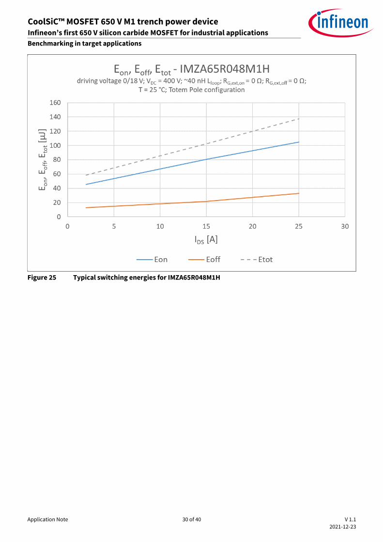
Figure 25 Typical switching energies for IMZA65R048M1H

Application Note 31 of 40 V 1.1
2021-12-23
CoolSiC™ MOSFET 650 V M1 trench power device Infineon’s first 650 V silicon carbide MOSFET for industrial applications
Benchmarking in target applications
Figure 26 Typical switching energies for IMZA65R072M1H
5.2 3.3 kW CCM totem pole PFC
The CCM totem pole PFC is the highest-efficiency bridgeless topology, achieving efficiency higher than 99
percent peak. 99 percent efficiency is necessary to achieve system efficiency of an SMPS of above 98 percent. This power supply is a 3.3 kW server power supply, a full Infineon solution using the IMZA6R048M1H as boost
stage including 600 V CoolMOS™ C7 17 mΩ devices as grid rectifier, Infineon 18 V auxiliary bias supply, XMC1404 and more. The input voltage is from 176 V AC to 360 V AC, fully capable of 3.3 kW output power at 400 V output
voltage and a switching frequency of 65 kHz. This board can also be equipped with the newest static switch
from Infineon technologies, the 600 V CoolMOS™ S7.

Application Note 32 of 40 V 1.1
2021-12-23
CoolSiC™ MOSFET 650 V M1 trench power device Infineon’s first 650 V silicon carbide MOSFET for industrial applications
Benchmarking in target applications
Figure 27 3.3 kW CCM totem pole PFC
Figure 28 shows the absolute efficiency over the output power at 230 V AC input voltage and 25°C ambient temperature, which was possible to achieve with the IMZA65R048M1H. The gray line corresponds to the
IMZA65R048M1H, which has more than 99 percent from 20 percent to 50 percent of load. Even with the
IMZA65R072M1H it is possible to achieve 99 percent peak efficiency and full capability to deliver the output
power down to 176 V AC. Also, the IMZA65R107M1H is able to come close to 99 percent peak efficiency and can
operate up to 3.3 kW at 230 V AC; nevertheless, by decreasing the input voltage the output power also needs to
be reduced due to thermal management. If the customer is willing to reduce the output power at lower input voltages it can lower costs significantly.

Application Note 33 of 40 V 1.1
2021-12-23
CoolSiC™ MOSFET 650 V M1 trench power device Infineon’s first 650 V silicon carbide MOSFET for industrial applications
Benchmarking in target applications
Figure 28 Efficiency comparison between CoolMOS™ and CoolSiC™
The best calculated efficiency which can be achieved in a dual-boost PFC by CoolMOS™ is represented as a
green line with a peak efficiency of 98.85 percent; nevertheless, this might result in an increased bill of
materials (BOM) cost due to the use of a synchronous grid, additional magnetics and space restrictions. It would be possible to further improve the efficiency using CoolMOS™ in a TCM totem pole PFC; this would result
in much higher driving and controlling complexity, and once again a higher part count.
All restrictions on VGS and 80 percent de-rating on VDS are applicable for CoolSiC™, and the best measurement
results in this design are obtained by the following external gate resistor selection.
Table 3 Used RG,ext values for the 3.3 kW CCM totem pole PFC
In order to operate the IMZA65R107M1H at lower input voltages and benefit from lower costs in a CCM totem pole PFC it is necessary to reduce the output power based on the decreased input voltage. According to this measurement the mold compound temperature was kept constant at 80°C at 25°C ambient.
Device RG,ext [Ω]
IMZA65R048M1H 6.4
IMZA65R072M1H 10
IMZA65R107M1H 15

Application Note 34 of 40 V 1.1
2021-12-23
CoolSiC™ MOSFET 650 V M1 trench power device Infineon’s first 650 V silicon carbide MOSFET for industrial applications
Benchmarking in target applications
Figure 29 Power de-rating need for low Vin for IMZA65R107M1H
In order to verify that the junction temperature is not exceeding the limit in the datasheet at 60°C ambient the assumption based on simulations is taken that the junction in this system has around 20°C higher temperature
than the mold compound. Under these conditions there is still enough safety margin. It can be clearly seen that it is possible to have full output power down to 220 V AC. Further increasing the input voltage leads to an
output power de-rating down to 2.5 kW at 176 V AC input voltage.
5.3 3 kW LLC converter
Due to the described technology parameters CoolSiC™ is also a very good fit for resonant topologies like the LLC converter. The body diode behavior can improve the system stability under certain operating conditions in which a hard commutation can occur.
This test board is based on telecom requirements with an input voltage of 380 V DC and an output power of 3 kW at 54 V output voltage. For the measurements only one rail of the dual phase was chosen in order to see the differences on the primary-side MOSFETs while not depending on the synchronous rectification on the
secondary stage.

Application Note 35 of 40 V 1.1
2021-12-23
CoolSiC™ MOSFET 650 V M1 trench power device Infineon’s first 650 V silicon carbide MOSFET for industrial applications
Benchmarking in target applications
Figure 30 Relative efficiency comparison with optimized body diode conduction time
This setup was introduced with CoolMOS™, and so the measurements can only show a comparison with
maximum 14 V gate driving.
The diode conduction times of silicon carbide devices have been measured. From this, the diode losses have
been calculated and implemented in the efficiency curves in order to get an estimation of the resulting efficiency in case optimized dead-times were used. This calculation has not been done for CoolMOS™ devices, since diode conduction time ‒ due to non-optimal dead-times ‒ is an almost-negligible contribution to the
overall efficiency. With these considerations, CoolSiC™ can have around 0.5 percent higher efficiency, especially at light load.
The diode conduction time is very important. The following efficiency comparison shows the impact of
CoolSiC™ forward voltage and an un-optimized dead-time setting. All devices present in this comparison have
ZVS. The board has a minimum dead-time of 200 ns, so a full optimization per device is not possible.

Application Note 36 of 40 V 1.1
2021-12-23
CoolSiC™ MOSFET 650 V M1 trench power device Infineon’s first 650 V silicon carbide MOSFET for industrial applications
Benchmarking in target applications
Figure 31 Relative efficiency comparison with 200 ns body diode conduction time
This leads to long diode conduction times, which will in turn lead to lower efficiency. Therefore, customers
need to take special care of the dead-time changes and be aware that plug-and-play is generally not
recommended in any resonant topology.

Application Note 37 of 40 V 1.1
2021-12-23
CoolSiC™ MOSFET 650 V M1 trench power device Infineon’s first 650 V silicon carbide MOSFET for industrial applications
Summary
6 Summary
In summary:
CoolMOS™:
• Cost-effective solution for SMPS up to 97 percent system efficiency
• Easy to use
• Most granular portfolio
• Proven quality
CoolSiC™:
• Cost-effective solution for SMPS greater than or equal to 97 percent system efficiency
• Easy to use, with recommended driving voltage of 18 V turn-on and 0 V turn-off
• Indicated for high-power applications
• Most suitable in any application where hard commutation on a conducting body diode is present or might
occur
Application Note 38 of 40 V 1.1
2021-12-23
CoolSiC™ MOSFET 650 V M1 trench power device Infineon’s first 650 V silicon carbide MOSFET for industrial applications
References
7 References
[1] P. Salmen, M. W. Feil, K. Waschneck, H. Reisinger, G. Rescher, T. Aichinger: A new test procedure to
realistically estimate end-of-life electrical parameter stability of SiC MOSFETs in switching operation (2021).

Application Note 39 of 40 V 1.1
2021-12-23
CoolSiC™ MOSFET 650 V M1 trench power device Infineon’s first 650 V silicon carbide MOSFET for industrial applications
Revision history
Revision history
Document
version
Date of release Description of changes
V 1.0 2020-01-16 Release of final version
V 1.1 2021-12-23 Gate driving guidelines

Trademarks All referenced product or service names and trademarks are the property of their respective owners.
Published by
Infineon Technologies AG
81726 Munich, Germany
© 2021 Infineon Technologies AG.
All Rights Reserved.
Do you have a question about this
document?
Email: [email protected]
Document reference
IMPORTANT NOTICE The information contained in this application note is given as a hint for the implementation of the product only and shall in no event be regarded as a description or warranty of a certain functionality, condition or quality of the product. Before implementation of the product, the recipient of this application note must verify any function and other technical information given herein in the real application. Infineon Technologies hereby disclaims any and all warranties and liabilities of any kind (including without limitation warranties of non-infringement of intellectual property rights of any third party) with respect to any and all information given in this application note. The data contained in this document is exclusively intended for technically trained staff. It is the responsibility of customer’s technical departments to evaluate the suitability of the product for the intended application and the completeness of the product information given in this document with respect to such application.
For further information on the product, technology, delivery terms and conditions and prices please contact your nearest Infineon Technologies office (www.infineon.com).
WARNINGS Due to technical requirements products may contain dangerous substances. For information on the types in question please contact your nearest Infineon Technologies office. Except as otherwise explicitly approved by Infineon Technologies in a written document signed by authorized representatives of Infineon Technologies, Infineon Technologies’ products may not be used in any applications where a failure of the product or any consequences of the use thereof can reasonably be expected to result in personal injury.
Edition 2021-12-23
AN_1907_PL52_1911_144109