Control of Electronic Coupling and Optical Properties in ... · Control of Electronic Coupling and...
132
Control of Electronic Coupling and Optical Properties in Quantum Dot Solids Dissertation der Fakultät für Physik der Ludwig-Maximilians-Universität München vorgelegt von Jianhong Zhang aus Shannxi (China) München, im September 2010
-
Upload
nguyenkhuong -
Category
Documents
-
view
214 -
download
0
Transcript of Control of Electronic Coupling and Optical Properties in ... · Control of Electronic Coupling and...

Control of Electronic Coupling
and Optical Properties in Quantum
Dot Solids
Dissertation der Fakultät für Physik der Ludwig-Maximilians-Universität München
vorgelegt von
Jianhong Zhang
aus Shannxi (China)
München, im September 2010

II
1. Gutachter: Prof. Dr. Jochen Feldmann
2. Gutachter: Prof. Dr. Alexander Högele
Mündliche Prüfung am 28. Oktober 2010
III
Publications on results of this thesis
• Thermomechanical control of electronic coupling in quantum dot solids
J. Zhang, A. A. Lutich, A. S. Susha, M. Döblinger, C. Mauser, A. O. Govorov,
A. L. Rogach, F. Jäckel, and J. Feldmann
Journal of Applied Physics 2010, 107, 123516
• Optical anisotropy of semiconductor nanowires beyond the electrostatic limit
J. Zhang, A. A. Lutich, J. Rodríguez-Fernández, A. S. Susha, A. L. Rogach, F. Jäckel,
and J. Feldmann
Phys. Rev. B 2010, 82, 155301
• Single-mode waveguiding in bundles of self-assembled semiconductor nanowires
J. Zhang, A. A. Lutich, A. S. Susha, A. L. Rogach, F. Jäckel, and J. Feldmann
Submitted

IV
Poster contributions to conferences and workshops
• Thermomechanic control of electronic coupling in polycrystalline semiconductor
nanowires
J. Zhang, A. A. Lutich, C. Mauser, J. Rodríguez-Fernández, A. S. Susha,
M. Döblinger, A. O. Govorov, A. L. Rogach, F. Jäckel, and J. Feldmann
NaNax 4- Nanoscience with Nanocrystals, Munich, 04/2010
• Controlling the electronic coupling in quantum dot solids-making photoluminescence
temperature independent
J. Zhang, A. A. Lutich, A. S. Susha, M. Döblinger, A. O. Govorov, A. L. Rogach,
F. Jäckel, and J. Feldmann
NRS 2009 Full Meeting, Boston, USA, 11/2009
• Thermomechanical control of electronic coupling in quantum dot solids
J. Zhang, A. A. Lutich, A. S. Susha, M. Döblinger, A. O. Govorov, A. L. Rogach,
F. Jäckel, and J. Feldmann
NIM workshop, Munich, 10/2009
• CdTe nanowires grown in solution using oriented attachment of spherical
nanocrystals
J. Zhang, A. S. Susha, A. L. Rogach, and J. Feldmann
NODE Summer School, Palazzone di Cortona (AR), Italy, 07/2008

V
To my parents
献给我的父母

VI

VII
Contents
Abstract .................................................................................................................................... IX
Kurzfassung..............................................................................................................................XI
1. Introduction ............................................................................................................................ 1
2. Background ............................................................................................................................ 7
2.1 Semiconductor nanocrystals............................................................................................. 7
2.1.1 Band gap in semiconductor materials ....................................................................... 7
2.1.2 Excitons in semiconductor materials......................................................................... 9
2.1.3 Excitons in semiconductor nanocrystals ................................................................. 10
2.2 Electronic coupling in quantum systems........................................................................ 12
2.2.1 Electronic interactions in the hydrogen molecule ................................................... 12
2.2.2 Electronic coupling in 1D quantum well superlattices............................................ 13
2.2.3 Electronic coupling in QD solids ............................................................................ 15
2.3 Oriented attachment of SNCs......................................................................................... 17
2.4 Propagation of electromagnetic waves........................................................................... 21
2.4.1 Maxwell’s equations in matter ................................................................................ 21
2.4.2 Optical anisotropies of 1D nanostructures .............................................................. 23
2.4.3 Waveguiding in 1D nanostructures ......................................................................... 26
3. Experimental ........................................................................................................................ 31
3.1 Materials and sample preparation .................................................................................. 32
3.1.1 Synthesis of CdTe nanocrystals .............................................................................. 32
3.1.2 Size-selective precipitation of CdTe nanocrystals .................................................. 33
3.1.3 Isolated CdTe NCs in a polyvinyl alcohol matrix................................................... 34
3.1.4 Densely packed CdTe NCs ..................................................................................... 34
3.1.5 Nanowires prepared from CdTe NCs...................................................................... 34
3.1.6 Nanoribbons prepared from CdTe NCs .................................................................. 38
3.1.7 Alignment of NWs .................................................................................................. 39
3.2 Experimental setups ....................................................................................................... 41
3.2.1 Absorption and photoluminescence spectroscopy .................................................. 41
3.2.2 Single-molecule spectroscopy................................................................................. 42
3.2.3 Dark field microscopy............................................................................................. 45
3.2.4 Time-correlated single photon counting ................................................................. 47
3.2.5 Optical lithography.................................................................................................. 48
3.2.6 Further devices used in this work............................................................................ 49
4. Thermomechanical control of electronic coupling in QD solids ......................................... 51

Contents
VIII
4.1 Electronic coupling in QD solids ................................................................................... 52
4.1.1 QD solids with different coupling strength ............................................................. 52
4.1.2 Photoluminescence at room temperature ................................................................ 54
4.1.3 Photoluminescence lifetime at room temperature................................................... 55
4.2 Thermomechanical control of electronic coupling......................................................... 56
4.2.1 Photoluminescence at 5K........................................................................................ 56
4.2.2 Electronic coupling in QD solids at different temperatures .................................... 58
4.2.3 Calculation of electronic coupling in QD solids ..................................................... 60
4.2.4 Composite nature of polycrystalline NWs .............................................................. 66
4.3 Conclusion...................................................................................................................... 68
5. Optical anisotropy of semiconductor NWs beyond the electrostatic limit........................... 71
5.1 Optical anisotropies in single NWs................................................................................ 72
5.1.1 Polarized photoluminescence from single NWs ..................................................... 73
5.1.2 Breakdown of the electrostatic limit ....................................................................... 74
5.1.3 FDTD calculations of polarization anisotropies...................................................... 76
5.1.4 Polarized scattering from single NWs..................................................................... 79
5.2 Optical anisotropies in NW arrays ................................................................................. 81
5.2.1 Disorder in NW arrays ............................................................................................ 82
5.2.2 Polymer environment .............................................................................................. 84
5.2.3 Multiple scattering................................................................................................... 84
5.3 Conclusion...................................................................................................................... 85
6. Nanoribbon waveguide ........................................................................................................ 87
6.1 Nanoribbons prepared by CdTe nanocrystals ................................................................ 88
6.2 Nanoribbon waveguides................................................................................................. 88
6.3 Single-mode nanoribbon waveguides ............................................................................ 90
6.4 Optical coupling between crossed nanoribbons ............................................................. 92
6.5 Losses studied by measuring the PL at tips as a function of excitation position ........... 93
6.6 Conclusion...................................................................................................................... 97
7. Conclusions and outlook ...................................................................................................... 99
Abbreviations ......................................................................................................................... 103
List of Figures ........................................................................................................................ 105
Bibliography........................................................................................................................... 109
Acknowledgements ................................................................................................................ 119

IX
Abstract In this thesis, we investigate the electronic coupling in quantum dot (QD) solids, optical anisotropies of nanowires (NWs) with diameters comparable to the wavelength of light, and the propagation of light in nanoribbon waveguides. In particular, we demonstrate a new mechanism to control the electronic coupling in QD solids thermomechanically, and how size controls the optical anisotropies in NWs.
We firstly demonstrate that the electronic coupling in QD solids can be controlled by a new thermomechanical mechanism. This mechanism is realized by controlling the expansion and shrinkage of the interstitial material in the QD solids, which in turn controls the distance and distance-dependent electronic coupling between semiconductor nanocrystals (SNCs). Photoluminescence (PL) and TEM investigation demonstrate the tuning of the band gap emission in individual polycrystalline NWs and densely packed SNCs via this mechanism. At low temperature, temperature-induced blueshift in densely packed SNC film and redshift in polycrystalline NWs were realized. This is qualitatively different from bulk CdTe and isolated CdTe SNCs. The electronic coupling between the nearest SNCs for sub-nm distances agrees well with semiempirical calculations.
Size dependence of optical anisotropies in NWs is demonstrated in this work. We found optical anisotropies in NWs with diameters comparable to the wavelength of light in the NW, i.e., beyond the electrostatic limit, are much lower than those of NWs in electrostatic limit. Finite-difference time domain calculations, with realistic parameters for the CdTe NWs, for excitation and PL anisotropy were carried out. It was found that the optical anisotropies of NWs display a strong size dependence when the NW is beyond the electrostatic limit. Changing the diameter allows tuning the polarization anisotropy from its maximum, predicted by the electrostatic limit, to zero. The optical anisotropies of a NW are determined by the diameter-wavelength ratio, the material dispersion, as well as the local refractive index of the surrounding. In addition, the optical anisotropies can be transferred into macroscopically aligned NW arrays, and the anisotropies of the NW arrays are determined by the optical anisotropies of isolated NWs, the disorder of the NWs in the film, the local environment and multiple scattering in the thick film.
Furthermore, we show that self-assembled nanoribbons can serve as single-mode waveguides for the propagation of PL light. Calculations show that the minimum width needed for single-mode operation is approximately 150 nm, which agrees well with SEM measurements. The loss in the nanoribbon waveguides was quantitatively determined. Re-absorption was demonstrated in the nanoribbon waveguides to be a major contribution in the loss mechanism. Losses in the nanoribbon waveguide are on the same order of magnitude as for plasmon waveguides.

Abstract
X

XI
Kurzfassung Im Rahmen dieser Arbeit untersuchen wir die elektronische Kopplung zwischen Quantenpunkten (QD) in QD-Festkörpern, optische Anisotropien von Nanodrähten (engl. Nanowires), deren Durchmesser vergleichbar mit der Wellenlänge im Material sind, sowie die Ausbreitung des Lichts in Nanoband (engl. Nanoribbon) Wellenleitern. Insbesondere demonstrieren wir einen neuen Mechanismus um die elektronische Kopplung in QD-Festkörpern thermomechanisch zu kontrollieren, und zeigen, wie die Größe die optische Anisotropie in Nanodrähten bestimmt.
Zunächst zeigen wir, dass die elektronische Kopplung in QD-Festkörpern durch einen neuen thermomechanischen Mechanismus kontrolliert werden kann. Dieser Mechanismus wird realisiert, indem die Ausdehnung und das Schrumpfen des Materials in den Zwischenräumen des QD-Festkörpers, welche wiederum den Abstand und somit die abstandsabhängige elektronische Kopplung zwischen den Halbleiter-Nanokristallen (SNCs) bestimmen, kontrolliert wurden. Photolumineszenz- (PL) und TEM-Untersuchungen veranschaulichen die Einstellung der Bandlücken–Emission in einzelnen polykristallinen Nanodrähten und dicht gepackten SNC-Filmen durch diesen Mechanismus. Bei tiefen Temperaturen wurden eine temperaturinduzierte Blauverschiebung in dicht gepackten SNC-Filmen und eine temperaturinduzierte Rotverschiebung in einzelnen polykristallinen Nanodrähten realisiert. Dies ist ein qualitativ neues Verhalten im Vergleich zu CdTe-Volumenkristallen und isolierten CdTe-SNC. Die elektronische Kopplung zwischen den nächstgelegenen Nachbarn im QD-Festkörper zeigt eine gute Übereinstimmung mit semiempirischen Rechnungen.
Des Weiteren wird in dieser Arbeit die Größenabhängigkeit der optischen Anisotropie in Nanodrähten untersucht. Wir zeigen, dass die optischen Anisotropien in Nanodrähten mit Durchmessern vergleichbar mit der Wellenlänge im Material, d.h. oberhalb des elektrostatischen Limits, kleiner sind als die von Nanodrähten mit kleineren Durchmessern.
FDTD–Rechnungen (engl. Finite-difference time domain) mit realistischen Parameter für die CdTe-Nanodrähte wurden für Anregungs- und Photolumineszenz-Anisotropie durchgeführt. Diese belegten, dass die optischen Anisotropien der Nanodrähte eine starke Größenabhängigkeit aufweisen falls der Durchmesser des Nanodrahts oberhalb des elektrostatischen Limits liegt. Änderungen des Durchmessers erlauben das Einstellen der Polarisationsanisotropie von ihrem Maximum bis zu null. Die optischen Anisotropien der Nanodrähte werden durch das Durchmesser-Wellenlänge-Verhältnis, die Materialdispersion sowie den Brechungsindex der Umgebung bestimmt. Außerdem bleiben die optischen Anisotropien einzelner Nanodrähte in Filmen makroskopisch ausgerichteter Nanodrähte größtenteils erhalten. Die optischen Anisotropien dieser Filme werden durch die optischen Anisotropien der einzelnen Nanodrähte, die Unordnung des Films, den Brechungsindex der Umgebung und durch multiple Streuprozesse in den dicken Filmen bestimmt.
Weiterhin zeigen wir, dass selbst-aggregierte Nanobänder als Einzelmoden-Wellenleiter für die Ausbreitung des Photolumineszenz-Lichtes fungieren können. Modellrechnungen zeigen, dass 150 nm als minimale Breite für den Einsatz als Einzelmoden-Wellenleiter notwendig sind. Diese Größe liegt in guter Übereinstimmung mit SEM-Experimenten. Die Verluste in Nanobänder wurden quantitativ bestimmt. Hierzu wurde gezeigt, dass die Reabsortion in den Nanobänder den Hauptanteil am Verlust-mechanismus darstellt. Die Verluste in den Nanobändern sind von derselben Größenordnung wie bei plasmonischen Wellenleitern.

Kurzfassung
XII

1
1. Introduction
Semiconductor nanocrystals (SNCs), also known as quantum dots (QDs), have attracted much
attention since they were discovered in the beginning of the 1980s [1]. SNCs, with sizes
between the molecular and solid state regime, confine the electrons and holes on the
nanometre scale. This gives rise to quantized electronic states which in turn control the optical
properties. Consequently, optical and electronic properties can be controlled by the size and
shape of the SNCs [2-5]. The controllable physical properties provide rich ground for basic
scientific research that has attracted considerable attention.
Because of their peculiar optical and electronic properties, SNCs are promising
components for applications in optoelectronic devices. The high luminescence efficiency and
the narrow spectral emission allow for the application of SNCs in light sources. When used in
hybrid light-emitting diodes (LEDs), the control of the colour of the emission can be achieved
by tuning the size of the SNCs due to the quantum size effect [6-7], and broad spectral
emission is generated by mixed monolayer of SNCs with different sizes in the hybrid
structures [8]. Optical gain in SNCs can overcome optical losses from scattering. As emission
wavelengths are tuneable with the size of SNCs, wavelength controlled lasing has been
demonstrated [9]. Classical light sources, such as LEDs and lasers, usually generate a large
number of photons obeying Poisson statistics. On the other hand, several applications in the
field of quantum information technology require light sources that can control the number of
photons. SNCs can be used for such applications and the controlled generation of single
photons can be realized using different methods [10-12]. Because SNCs have a larger
interfacial area for change transfer than bulk materials, they are also used in solar cells.
Compared to organic solar cells, the higher electron mobility in SNCs can improve the
efficiency [13-15] of solar cells. W. U. Huynh et al. have investigated the efficiency of
nanorod-polymer solar cells with nanorods of different morphologies, and they found the

Chapter 1. Introduction
2
charge transport in the solar cells depends on the length of nanorods [13]. Single-electron
transistors based on the Coulomb blockade in the tunnel junctions have also been designed
using SNCs [16-17]. At present, SNCs are mostly used in the field of biology. The broad
absorption spectra of SNCs enable excitation by a wide range of wavelengths. Because SNCs
are extremely bright and photostable, they can be used as cell markers in the field of live-cell
imaging [18-22]. SNCs can also be used as ion probes and pH sensors because the
luminescence intensity of SNCs is affected by the ionic environment and the pH [23-25].
SNCs can self-assemble to give extended arrays, called QD solids. This kind of artificial
solids exhibits tuneable optical and electronic properties [26-27], and offers opportunities to
explore cooperative physical phenomena and to engineer the optical and electronic properties
of materials on the nanometre scale. The optical and electronic properties of these systems are
determined by the electronic structures of the SNC building blocks and the interactions
between them. The former can be controlled by the material, size and shape of SNCs [2-5].
And the latter, the electronic coupling between them, is tuneable by adjusting the distance
between the SNCs [27]. The control of the electronic coupling in QD solids by the adjustment
of the capping group of SNCs [28], or by removing the ligands to reduce the distance between
SNCs [29] has been reported. As the expansion and shrinkage of a solid can be controlled by
temperature, it is interesting to know if the electronic coupling can be controlled
thermomechanically, i.e., by controlling the separation between SNCs with temperature. In
this work, we will explore the possibility of thermomechanical control of electronic coupling
in QD solids.
Since the 1990s, quasi one-dimensional (1D) semiconductor nanostructures, i.e.,
nanowires (NWs) and nanoribbons, have emerged [30]. These structures have cross-sections
of 2–200 nm and lengths up to several micrometers. SNCs confine charge carriers in all three
dimensions and consequently the band gap depends on the size of the SNCs. Different from
SNCs, in the 1D nanostructures, charge carriers are confined only in two dimensions. The size
dependence of the band gap has also been observed due to quantum confinement [31-32], and
the band gap increases as the diameter of the quantum wire decreases. The high-aspect-ratio
of the 1D nanostructures allows for the bridging between the nanoscopic and macroscopic
world. And the 1D nanostructures were recognized as the essential building blocks for
electrical or optoelectronic devices [33-35].

Chapter 1. Introduction
3
The appearance of 1D nanostructures attracted much attention and much work has been
centred on the synthesis of 1D semiconductor nanostructures for specific applications.
Catalysts are most frequently used to prepare nanostructures from vapour [36-40] or in
solution [41-43]. Investigation on the growth mechanism shows that the diameter of the
product is controlled by the size of the catalyst [44]. This method is mostly used to prepare
single crystalline NWs with high electrical conductivity. Catalysts are also employed to
prepare p-n junction NWs, or grow a QD in the NW, or even prepare NW superlattices, by the
modulation of the reactants during growth [45-47]. Besides catalysts, templates are also
commonly used for the preparation of 1D nanostructures [48-52]. The underlying idea is the
crystallization of semiconductors within the restricted environment of the template. The
template serves as a scaffold in this method against which other materials with similar
morphologies are synthesized. Another method to prepare 1D semiconductor nanostructures
is the oriented attachment of SNCs [53-56]. This method is used in this work, and it will be
discussed in detail in chapter 2.
1D semiconductor nanostructures show important applications in diverse areas. As
discussed above, using catalysts, p-n junctions and even QDs can be synthesised in the NWs.
NW p-n junctions used for LEDs can control electrical injection along the wire [47, 57]. A
QD grown within a p-n diode can precisely define the emission in the QD region [58].
Because semiconductor NWs with high surface-volume ratio allow for fast electron transport
along the NWs, compared to SNCs, semiconductor NWs are preferred in solar cells [59]. As
the binding of charged molecules will result in depletion or accumulation of carriers and
change the conductance of NWs, NW-based field-effect transistors can be used as sensitive
chemical and biological sensors [60-65]. Another interesting property of 1D semiconductor
nanostructures is their optical anisotropy [66-67]. The anisotropies of thin NWs mainly
originate from the dielectric mismatch between the 1D nanostructure and the surrounding
environment, and the polarized properties of 1D nanostructures allow for their applications as
polarized light sources [47] and detectors [68]. In this work, we will investigate the optical
anisotropies of NWs with diameters comparable with the wavelength of light in the NWs, and
to explore if the optical anisotropies depend on the size of the NWs.
For some applications of 1D nanostructures in optical, electronic and optoelectronic
devices, it is important to transfer the properties of individual NWs into large NW arrays.
Aligned NWs have already shown their advantages in many fields, for example, crossed NWs
Chapter 1. Introduction
4
are used in LEDs to control the colour of the emitted light [69]; NW arrays are used in solar
cells to increase the efficiency of the solar cells [70-71]; integrated NW array sensors, in
which distinct NWs were incorporated as individual device elements, can largely increase the
sensitivity [64]; and also aligned 1D nanostructure arrays can be used as polarized light
source or detector [72-74]. The alignment of NWs in a particular direction is an attractive
topic, and external forces are used for this purpose, including electric fields [35, 73, 75-77],
templates [78-80], Langmuir−Blodgett techniques [81], or stretching of polymer film [82-83].
In this work, NWs were aligned in polymer film. We will study the optical anisotropies of
NW arrays, combining with those of single NWs.
In integrated photonic circuits, photons are required to be precisely delivered between
different components, and the development of 1D semiconductor nanostructure waveguides is
an important step towards this end. The dielectric contrast between the semiconductor and its
surrounding enables the confinement of the wave in the nanostructure and propagation along
the axis [84-87]. With flat reflecting end facets, the nanostructure can serve as an axial Fabry-
Pérot cavity. In addition, the semiconductor nanostructures represent an optical gain medium
and above a certain threshold of incident pump power, lasing was observed [88-89]. In this
work, the propagation of light in the nanoribbon waveguides will be investigated.
This work aimed at exploring possibilities to control the electronic coupling in QD solids,
to study size dependent optical anisotropies and propagation of light in 1D semiconductor
nanostructures, as well as possible applications.
This thesis consists of seven chapters, and it is arranged in following way. After this
general introduction of SNCs, the background needed for the understanding of the work
presented in this thesis is introduced in chapter 2. Since 1D semiconductor nanostructures
investigated in this thesis are prepared from SNCs, the fundamentals of semiconductors and
SNCs are firstly reviewed, followed by the interactions between SNCs in the QD solids and
the oriented attachment of SNCs into 1D nanostructures. In 1D semiconductor nanostructures,
dielectric screening can lead to optical anisotropies and total internal reflection can restrict
and guide the waves to propagate along the nanostructures. As optical anisotropies and
waveguiding are studied in this work, we will discuss how electromagnetic waves are passing
through or propagating in materials.
Chapter 3 describes the materials and experimental methods used in this work.

Chapter 1. Introduction
5
In chapter 4, we demonstrated the thermomechanical control of electronic coupling in QD
solids by controlling the expansion and shrinkage of inter-particle distance with temperature.
The size-dependent optical anisotropies in semiconductor NWs were demonstrated in
chapter 5. And the anisotropies of single NWs were transferred into macroscopically aligned
NW arrays.
In chapter 6, we investigated the propagation of waves in the nanoribbon waveguides.
The work ends with a conclusion and outlook.

Chapter 1. Introduction
6

7
2. Background
This chapter gives an introduction to the background needed for the understanding of the
work presented in this thesis. We firstly describe the fundamentals of semiconductor and
semiconductor nanocrystals. Afterwards interactions between SNCs in QD solids are
presented. Oriented attachment of SNCs, which is the method to prepare quasi one-
dimensional semiconductor nanostructures in this work, is introduced. In addition, we will
introduce how waves are passing through different mediums or propagating in the same
medium.
2.1 Semiconductor nanocrystals
Semiconductor nanocrystals have received growing interests because of their high
luminescence efficiency (on the order of 10%) and size controllable optical and electronic
properties [2-5]. In this work, CdTe SNCs are building block of 1D polycrystalline
nanostructures. In what follows, the fundamental properties of semiconductor and SNCs are
presented.
2.1.1 Band gap in semiconductor materials
The properties of a solid are significantly determined by the arrangement of the atoms in the
form of a periodic lattice with a lattice vector R . The electrons in the solids not only have
interactions with atomic nuclei, but also with other electrons. Assuming that all the
interactions between electrons and nuclei are described by an effective potential )(rU , the
electronic properties of a solid can be examined by the time independent Schrödinger
equation 2.1 [90]

Chapter 2. Background
8
)()(2
)( 22
rrUm
rE ψψ ⎟⎟⎠
⎞⎜⎜⎝
⎛+∇−=
h (2.1)
Here, )(rψ is the wave function for one electron. One of the most important properties of the
potential )(rU is that it is periodic on a lattice, i.e., )()( RrUrU += . Independent electrons,
which obey a one-electron Schrödinger equation 2.1 with a periodic potential, are known as
Bloch electrons.
At the edge of the Brillouin zone, the strong scattering produces standing waves of the
electron wave function and different distributions of the charge density arise. The
distributions with different energies are the origin of the band gap [91].
The band structures of many semiconductor materials have been calculated by M. L.
Cohen and T. K. Bergstresser [92]. Figure 2.1 shows the band structure of CdTe, the material
of which SNCs are investigated in this work. One can see that there are energies that are not
allowed at a temperature T = 0. For CdTe, all states of the valence band are filled, while the
states in the conduction band are empty. The minimum of the conduction band and the
maximum of the valence band appear at the same wave vector, which makes CdTe a direct
band gap semiconductor. Because the band gap is rather small, electrons may be excited
thermally at room temperature from the valence band to the conduction band. Generally
speaking, the number of excited electrons is appreciable (at room temperature) when the
energy gap is smaller than 2 eV.
Figure 2. 1: Band structure of CdTe. Reprinted figure with permission from [92]. Copyright 2006 by
the American Physical Society.

2.1 Semiconductor nanocrystals
9
The band gap of a semiconductor, however, depends strongly on the temperature of the
material. This behaviour is described by a simple formula by Y. P. Varshni [93]:
TTETE GG +
−=βα 2
)0()( (2.2)
Here )0(GE is the band gap at T = 0 K, α and β are empirical parameters. The band gap of
bulk CdTe is 1.51 eV at room temperature and it increases to 1.61 eV at liquid helium
temperature [94]. The band widening of CdTe at low temperature is explained by the
shrinkage of the crystal lattice and reduced phonon scattering [95].
2.1.2 Excitons in semiconductor materials
The excitation of electrons to the conduction band can be realized by the absorption of
photons of appropriate energy. When electrons are excited across the gap, the bottom of the
conduction band is populated by electrons, and the top of the valence band by holes. The
electron and hole are bound as a pair by Coulomb attraction and the bound state is called
exciton. The exciton has an energy slightly lower than an unbound electron-hole pair, and the
quantum mechanical description of excitons is similar to the one of hydrogen atom. The
energy of the exciton can be described in equation 2.3 [90]
re
mP
mP
Eh
h
e
e
0
222
422 πεε−+= ∗∗ (2.3)
Here, ∗em and ∗
hm are the effective masses of the electron and hole, respectively. ε is the
dielectric constant of the semiconductor. The first two terms are the kinetic energies of
electron and hole, and the last term corresponds to the attractive Coulomb interaction.
With the known solutions for the hydrogen atom [90], the energy levels of an exciton are
given by
⎥⎥⎦
⎤
⎢⎢⎣
⎡⎟⎟⎠
⎞⎜⎜⎝
⎛−=
2
0
2
22 421
πεεµ e
nEn
h (2.4)
Here µ is the reduced mass given by

Chapter 2. Background
10
∗∗ +=he mm
111µ
(2.5)
The Bohr radius of the exciton is given by
2
204
eaB µ
πεε h= (2.6)
Charge carriers in semiconductors normally have relatively low effective mass and the
refractive index of the materials is high, so that the Bohr radius of the exciton is typically
about several nm [96].
2.1.3 Excitons in semiconductor nanocrystals
In bulk semiconductor, excitons are delocalized on the scale of the Bohr radius. But SNCs
with size smaller than the Bohr radius strongly confine the wave functions of electrons and
holes in all three dimensions, and the charge carriers have to assume higher kinetic energies
leading to an increasing band gap and quantization of the energy levels to discrete values.
Such three-dimensional confinement effects collapse the continuous density of states of the
bulk solid into the discrete electronic states of the SNC [97]. Figure 2.2 shows how the
density of states changes with energy for semiconductor structures with different geometries.
SNCs, belonging to 0-dimensional case, have discrete energy levels.
Figure 2. 2: Density of states of a charge carrier confined in different dimensions. Eg is the band gap
of bulk semiconductor.
Semiconductor nanocrystals, with a size of several nanometres have some peculiar and
fascinating properties and applications superior to both bulk and molecular systems. Strong
photoluminescence and size-dependent optical and electronic properties are most promising
features of SNCs [3-4]. The finite size of the SNC quantizes the allowed wave vector (k)

2.1 Semiconductor nanocrystals
11
values. Decreasing the size of SNC shifts the first states to larger k values and increases the
energetic separation between the states. Spectroscopically, the blueshift of the PL and
absorption was observed when decreasing the diameter of SNCs, indicating the increase of
quantum confinement [98-100]. (Figure 2.3)
Figure 2. 3: (a) Energy diagrams illustrate that decreasing the diameter of the SNCs shifts the first
state to larger values of k and increases the energetic separation between states. (b) PL image and (c)
absorption and PL spectra of CdTe NCs with different diameters. The arrows in (b) and (c) indicate
the decreasing the size of SNCs. Reprinted with permission from [100]. Copyright 2002 American
Chemical Society.
The quantum states of charge carriers in the SNCs can be considered as those of a particle
in a central potential )(rU [90]. If the Coulomb interaction between electron and hole is
considered, the Hamiltonian of the system is given by
he
hheehh
ee rr
erUrUmm
H−
−++∇−∇−= ∗∗
0
22
22
2
4)()(
22 πεε
hh (2.7)
For CdTe, the effective masses of the electrons and holes are 0.096 m0 [101] and 0.37 m0 [102]
with m0 the free electron mass, respectively. So the effective masses of the two charges are
only a small fraction of an electron mass, implying the large localization energies for electron
and hole. The dielectric constant of inorganic semiconductors is very large, for example, bulk

Chapter 2. Background
12
CdTe has a dielectric constant between 12 and 9 in the UV-Vis spectral range [103], the
Coulomb interaction is very small and can be considered as a perturbation [96].
L. E. Brus built a model to explore the relationship between band gap and the size of
SNCs [96]. In this model, the kinetic energy is treated by the effective mass approximation,
and Coulomb interaction is considered. An approximate formula is given for the lowest
excited electronic state energy by solving Schrödinger equation. The band gap gE can be
approximately written as [96, 104]
Re
eREE bulk
gg0
2
2
22
48.11
2 πεεµπ
−+≅h (2.8)
Here, bulkgE is the bulk energy gap, R is the particle radius, µ is the effective mass of the
exciton, ε is the relative permittivity, and e is the charge of the electron. It can be seen that the
band gap is increasing by decreasing the size of nanoparticles.
2.2 Electronic coupling in quantum systems
SNCs have interesting properties and promising applications in many fields [6-7, 23-25],
however, the optical and electronic properties of individual SNCs can be modified via
electronic coupling between densely packed SNCs. The electronic coupling between SNCs is
investigated within the course of this work. In this section, the fundamental principles of such
electronic coupling will be introduced.
2.2.1 Electronic interactions in the hydrogen molecule
Electronic coupling not only occurs between SNCs, but also occurs between atoms or
molecules. When atoms or molecules organize into condensed systems, new collective
phenomena develop. The simplest case is the hydrogen molecule, H2, which can be
considered to be made up of two separate protons and electrons. The electrons in isolated
hydrogen atoms occupy atomic orbitals, and the spatial wave functions are schematically
illustrated in figure 2.4 (a) and (b). When the hydrogen atoms are bound to form a molecule,
there are two molecular orbitals formed due to the interaction between the electrons. The
lower energy orbital, called the bonding molecular orbital, with the wave function shown in
figure 2.4(c), has significant electron density between the two nuclei. While the antibonding

2.2 Electronic coupling in quantum systems
13
molecular orbital has a vanishing electron density in the centre and it has higher energy than
the atomic orbitals (Figure 2.4(d)).
Figure 2. 4: (a), (b) The spatial wave function of electrons in isolated hydrogen atoms, and the wave
functions of a hydrogen molecule for the bonding state (c), which has lower energy than the atomic
orbitals, and the antibonding state (d) with higher energy.
2.2.2 Electronic coupling in 1D quantum well superlattices
Like atoms or molecules, but in the next level of hierarchy, SNCs may also be used as the
building blocks of condensed matter. The exciton in SNCs is similar to the hydrogen atom,
and electronic coupling will occur when the distance between the SNCs is comparable to
atomic distance. As an introduction to the interactions between neighbouring SNCs, we start
with 1D quantum well superlattices.
Figure 2. 5: Potential and subband energy diagrams of (a) isolated quantum well and (b) superlattice.
In the superlattice, confined states in isolated quantum well expand to form minibands.

Chapter 2. Background
14
We assume that the superlattice is composed of smaller-band gap (EgW) quantum well
layers with a thickness of LZ, and the larger-band gap (EgB) barriers with a width of LB. In the
case of an isolated quantum well, confined subband states, formed due to quantum size effect,
are localized in the particular well regions shown in figure 2.5(a). However, in the
superlattices, the confined states are degenerate in energy and can couple through the thin
barriers by tunnelling, the envelope wave function is delocalized and spread over all wells,
and the original states expand to form minibands, as illustrated in figure 2.5(b) [105].
1D minibands are formed for the tunnelling of both the electrons and holes. The width of
the miniband, ∆2 , depends on how much the wave function can penetrate into the classical
forbidden area, and it can be calculated based on the Kronig-Penney model [106] using the
effective mass approximation. The eigenvalue of energy can be calculated from the following
equation:
[ ] )cos()cosh()sin()sinh(21)(cos ZBZB
W
B
B
WBZ kLLkLL
mkm
kmm
LLK θθθ
θ+⎟⎟
⎠
⎞⎜⎜⎝
⎛−=+ ∗
∗
∗
∗
(2.9)
where 22 2
h
Emk W
∗
= and 22 )(2
h
EVmB −=
∗
θ
V denotes the band offset between the quantum well and the barrier, h is Plank’s constant
divided by π2 , ZL and BL are the thickness of the quantum well and barrier, K is the wave
vector, and ∗Wm and ∗
Bm are the effective masses of the quantum well and barrier materials,
respectively.
The width of the miniband for GaAs/AlAs superlattice is calculated [105], and the
calculation is schematically shown in figure 2.6. It allows the following conclusions [105]: (1)
If the thickness of the quantum well ( ZL ) stays constant, the coupling of the electronic wave
function decreases with increasing barrier thickness. (2) If the barrier stays constant,
decreasing the thickness of the quantum well will increase the energy of the subband states.
The coupling strength is illustrated in figure 2.6(a) as ∆2 . (3) The calculations [105] indicate
that the width of the miniband can be tuned between zero and a few hundred meV. (4) The
width of the heavy-hole miniband is narrower than that of electron miniband, because of
larger effective mass (figure 2.6(b)). These phenomena are experimentally confirmed by
absorption spectra [107]. By decreasing the barrier thickness, the absorption edge shifts to

2.2 Electronic coupling in quantum systems
15
lower energies, indicating the enhancement of resonant coupling through the tunnelling
process between the quantum wells.
Figure 2. 6: Schematic illustration of minibands for (a) electrons in different quantum wells and (b)
electrons and holes in the same quantum well in GaAs/AlAs superlattices.
2.2.3 Electronic coupling in QD solids
As synthetic techniques have developed for producing SNCs with very narrow size
distributions, they may also be used as the building blocks of condensed matter. Many
artificial SNCs structures, like ordered arrays of SNCs or SNC superlattices [27], SNC
particle chains [108], conjugates of NWs and SNCs [109], and SNC bilayers [110-111] have
been built. In the NC assemblies, which are also called QD solids, the strong confinement of
electrons and holes within isolated SNCs can be relaxed by tunnelling of charge carriers
between neighbouring SNCs. So the properties of SNC assemblies are determined not only by
the SNC units but also by the interactions between neighbouring SNCs. The new collective
phenomena in the artificial SNC structures offer enormous possibility in the design of novel
materials with controlled optical and electronic properties. Furthermore, such materials
provide a unique model system for the study of fundamental physical processes, such as
charge carrier transport, exciton diffusion, and energy transfer. They also open up the
possibilities of fabricating new solid state materials and devices with novel physical
properties.
Chapter 2. Background
16
Similar to 1D quantum well superlattices, the control of the optical and electronic
properties of QD solids can be realized by controlling the SNC units or the coupling between
them.
The coupling strength in the QD solids depends on the distance between the adjacent
SNCs. When the inter-particle separations is between 0.5 and 10 nm, the interaction between
proximal SNCs is dominated by dipolar coupling [27]. The dipoles in SNCs arise from
oscillations in charge distributions as SNCs change eigenstate, and dipole-dipole interactions
lead to electronic energy transfer. Energy transfer often occurs in solids containing two sizes
of SNCs, one called the donor and the other the acceptor. The acceptor has both a transition in
resonance with the energy of donor emission and a lower energy state in which to trap the
transferred excitation. Once the transferred excitation is trapped in the lower energy state of
the acceptor, the excitation cannot be transferred back because the donor is transparent to the
lower energy excitation. Energy transfer is measured spectroscopically by the quenching of
the PL quantum yield of the donor, or by the accompanied enhancement of the PL quantum
yield of the acceptor. Energy transfer was experimentally realized in many artificial SNC
assembles, for example, the mixture of different SNCs [112], layer-by-layer assembled
bilayers of SNCs with different sizes [113], SNCs electrostatically bound by ions [114], or
even transfer from organic dye molecules to SNCs [115].
When the distance between SNCs is smaller than 0.5 nm, exchange interactions become
significant, and electronic excitations are delocalized over many SNCs. S. V. Gaponenko et al.
[26, 116-117] showed that in close-packed QD solids, the electronic wave functions of the
SNCs extended toward neighbouring SNCs. In the case of densely packed SNCs, the
exchange interactions become significant and electronic excitations become delocalized.
When the size of the SNCs decreases, the electronic wave functions from the SNC states spill
further outside the volume of the SNCs, and the optical spectra of close-packed SNC solids,
prepared from the smallest CdSe NCs, are similar to those of bulk CdSe [117].
Consequently, the control of the optical and electronic properties of QD solids can be
achieved by controlling the size and material of the SNCs, or by tuning the separation
between SNCs. The first mechanism is based on the quantum size effect, and the second is
based on the distance dependent coupling. Usually, SNCs are capped by ligands, and the
control of the inter-particle distance can be realized by adjusting the size of capping groups
SNCs [28] or by removing the ligands [29, 118].

2.3 Oriented attachment of SNCs
17
Electronic coupling can also be investigated using scanning tunnelling microscopy and
spectroscopy at low temperature. The investigation of quantum mechanical coupling in two-
dimensional (2D) arrays of PbSe NCs has been reported by P. Liljeroth et al. [119]. PbSe has
low effective masses of both the electron and hole, which lead to an increased extension of
the wave function outside the SNC and an increased coupling between adjacent SNCs. By
comparing the tunnelling spectra of isolated SNC (figure 2.7(a)) and single SNC in SNC
arrays (figure 2.7(b)), predominant coupling between individual NC in the 2D array was
found with a coupling strength of 50-150 meV between the electronic states. In some regions,
the strong coupling of both the conduction and valence levels was observed.
Figure 2. 7: Experimental dVdI spectra measured on (a) an isolated QD and (b) different QDs in
the QD arrays. Reprinted figure with permission from [119]. Copyright 2006 by the American
Physical Society.
In this work, investigation of electronic coupling between SNCs in QD solids is carried
out spectroscopically on polycrystalline NWs, which have inter-particle distances smaller
than 0.5 nm due to organic ligands. The NWs are prepared by the oriented attachment of
CdTe SNCs. In what follows, this method is introduced.
2.3 Oriented attachment of SNCs
1D nanostructures can be prepared using catalysts [43-50] or templates [48-52]. Comparing to
these two methods, the growth of 1D semiconductor nanostructures by the oriented
attachment of SNCs is a new method. This method was first reported by R. L. Penn and J. F.
Banfield in 1998 [53-54]. In this process, the adjacent SNCs organize spontaneously, and the
Chapter 2. Background
18
coalescence of primary SNCs in specific crystallographic orientation is caused by the
difference of surface energy at each face.
In this work, 1D semiconductor nanostructures are prepared by the oriented attachment of
CdTe SNCs. As CdTe SNCs have been reported to have many important applications in
photovoltaic devices [120], and biolabeling and detection [121-122], preparation of
nanostructures using CdTe SNCs has attracted much attention [55, 123-125]. The
semiconductor nanostructures prepared using CdTe SNCs are expected to enhance or modify
the optical and electronic properties of their units.
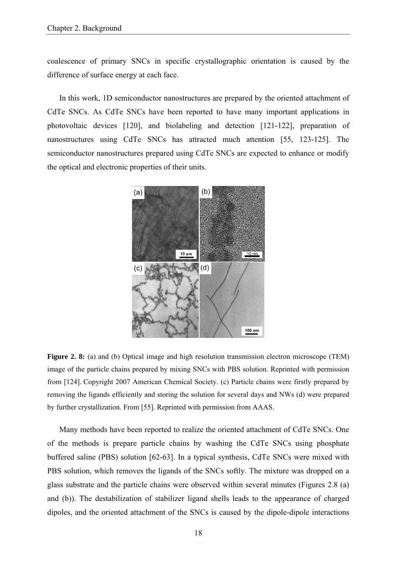
Figure 2. 8: (a) and (b) Optical image and high resolution transmission electron microscope (TEM)
image of the particle chains prepared by mixing SNCs with PBS solution. Reprinted with permission
from [124]. Copyright 2007 American Chemical Society. (c) Particle chains were firstly prepared by
removing the ligands efficiently and storing the solution for several days and NWs (d) were prepared
by further crystallization. From [55]. Reprinted with permission from AAAS.
Many methods have been reported to realize the oriented attachment of CdTe SNCs. One
of the methods is prepare particle chains by washing the CdTe SNCs using phosphate
buffered saline (PBS) solution [62-63]. In a typical synthesis, CdTe SNCs were mixed with
PBS solution, which removes the ligands of the SNCs softly. The mixture was dropped on a
glass substrate and the particle chains were observed within several minutes (Figures 2.8 (a)
and (b)). The destabilization of stabilizer ligand shells leads to the appearance of charged
dipoles, and the oriented attachment of the SNCs is caused by the dipole-dipole interactions

2.3 Oriented attachment of SNCs
19
between spherical SNCs. As prepared particle chains are not stable and can be dispersed as
individual SNCs in water. Another method was reported by N. A. Kotov’s group [55]. They
found that negatively charged zincblende CdTe NCs can spontaneous self-assembly into NWs.
NW formation was initiated by removing the stabilizer efficiently by washing with methanol
followed by centrifugation. The precipitate was then redispersed in water at pH 9 and allowed
to age at room temperature in the dark for several days. During this period, SNCs firstly
connected to form particle chains (Figure 2.8(c)), and over 7 days, the colour of the solution
gradually turned from orange to dark brown or black, and NWs were observed in the solution
(Figure 2.8(d)).
The oriented attachment of SNCs has attracted much interest because it is a general
method applicable in principle to all colloidal SNCs [65-71], and materials with controlled
size and morphology can be designed using this method.
The shape and property of the nanostructures prepared by the oriented attachment of
SNCs depend on the primary SNCs. For example, the choice of the SNC size offers a suitable
way to control the extent of quantum confinement and morphology of the NWs. Single
crystalline NWs were prepared by the oriented attachment of CdTe NCs by Z. Y. Tang et al.
The diameters of the NWs are identical to the diameters of precursor nanoparticles, and the
emission wavelength of the NW luminescence can be easily tuned by sizing the starting
nanoparticles [55].
Materials with controlled size and morphology can also be realized by controlling the
growing conditions during the oriented attachment. PbSe NWs with different thickness and
even smooth, single crystalline rectangular nanorings were controllably realized at different
conditions [126]. By the modulation of surface energies of the different crystallographic faces,
nanostructures with shape evolves from bullet and diamond structures to rods and branched
rods were prepared [127].
At present, the detailed assembly process is not fully understood, and it is considered that
charged dipoles are induced by the removal of ligands and oriented attachment in the
formation of nanostructures involves dipole–dipole attractions between SNCs [55]. From a
thermodynamical point of view, the combination in a coherent crystallographic orientation
will eliminate the interfaces and the surface energy of SNCs will be reduced in this process.

Chapter 2. Background
20
The difference of surface energy at each face leads to the coalescence of primary particles in
specific crystallographic orientation and oriented attachment based growth [56].
Simulations of the oriented attachment process of CdTe nanoparticles into NWs was also
reported [128]. In this simulation, the SNCs were assumed to have the shape of a truncated
tetrahedron. The direction of the dipole moment is strongly dependent on the number of
truncations. The oriented attachment depends on the face-face attraction between SNCs and
the repulsion caused by the charges. The delicate balance of various anisotropic interactions
between the SNCs is responsible for the assembly.
Not only QDs can grow into 1D nanostructures by oriented attachment, but also nanorods
or NWs can attach to build different morphologies [129]. Nanorods with diameters between
20 and 1000 nm were reported to axially self-assemble into multisegmented coaxial NWs by
an end-to-end self-assembly process (Figure 2.9(a)). While NWs with diameter of 10~30 nm
aligned side-by-side to form nanoribbons (Figure 2.9(b)).
Figure 2. 9: Illustration of end-to-end oriented attachment assisted self-assembly of nanorods into
multisegmented coaxial nanowires (a) and side-by-side oriented attachment assisted self-assembly of
nanowires into nanobelts (b). Reprinted with permission from [129]. Copyright 2007 American
Chemical Society.
The end-to-end attachment is due to high-energy crystal face on the tips of nanorods. The
high-energy faces act as the sticky points to induce the nanorods to join in the ends. As a
result, the nanorods attach end-by-end along the axis of the nanorods to form NWs. Lateral
oriented attachment occurs when the energy of the crystal face of the side is adequate for

2.4 Propagation of electromagnetic waves
21
NWs to align side-by-side and to form NW bundles. Nanobelts were prepared by the further
crystallization of the NW bundles through oriented attachment. In this work, polycrystalline
semiconductor NWs were prepared by the oriented attachment of CdTe NCs, and nanoribbons
were prepared by the side-by-side alignment of NWs.
2.4 Propagation of electromagnetic waves
1D semiconductor nanostructures prepared by the oriented attachment of CdTe SNCs in this
work have high-aspect-ratio and large dielectric constant [103]. They have promising shapes
for applications in the field of polarization and waveguiding. In this work, we investigate how
light is emitted/absorbed between NWs and the surrounding, and how it is guided to
propagate in nanoribbons. The basic knowledge on how electromagnetic waves passing
through different mediums or propagating in the same medium will be introduced in the
following section.
2.4.1 Maxwell’s equations in matter
To understand how light is passing through or propagating in the 1D semiconductor
nanostructures, we need to know the physical process when electromagnetic waves propagate
in nanostructures and the surrounding medium. Maxwell’s equations are the fundamental
equations describing the evolution of electromagnetic fields in the presence of charges,
current, and media. This set of equations includes Gauss’ (2.10 and 2.11), Faraday’s (2.12),
and Ampère’s (2.13) laws. They relate the electric flux density D (C/m2), electric field E
(V/m), magnetic flux density B (T = Wb/m2), magnetic field H (A/m), charge density ρ
(C/m3), and current density J (A/cm2), to one another in space and time [130], as
ρ=⋅∇ D (2.10)
0=⋅∇ B (2.11)
dtBdE −=×∇ (2.12)
Chapter 2. Background
22
dtDdJH +=×∇ (2.13)
When the electrodynamic theory is used to describe the interactions of matter with electric
and magnetic fields, some material properties (for example, the complex dielectric function)
enter as input parameters. The material dependent parameters are taken either from
experimental data or calculations by solid state theory. And the changes in the material
properties induced by the interaction with electromagnetic field cannot be explained by
classical electrodynamics.
To distinguish external fields and fields produced by the response of the material, the
electric flux density D and the induced electrical polarization P (C/m2) are related to E by
EEEEEDP m χεεεεεεεεε 000000 )1()()( =−=−=−=−= (2.14)
mε represents the permittivity (F/m). ε is the dielectric constant, a dimensionless term. And
the susceptibility χ is defined as
IR iχχεχ +=−= 1 (2.15)
Microscopically, the real part of the susceptibility χ is derived from the dipole response of
atoms and electrons in the material to an electromagnetic wave, which is the basis of
polarization.
Likewise, the magnetic field vector H is related to the magnetic flux density B by
HB mµ= , mµ represents the permeability (H/m).
Since the spatial variation of E is related to a time variation of H and vice versa, the
propagation of electromagnetic waves can be described explicitly by means of a wave
equation.
If we assume that the electric field propagates in the z direction, λπ2
=k is the
propagation constant in the material, and ω is the angular frequency, then in the case where
0=ρ , the electric field and the polarization term P can be described as plane waves:

2.4 Propagation of electromagnetic waves
23
)(0
tkzieEE ω−= and )(0
tkziePP ω−= (2.16)
The electric field can be presented by the components of absorption, propagation and time
dependence of a wave in a material:
tizikzeeeEE Z ωα −−
⋅⋅= 21
0 (2.17)
Here, α is the intensity loss coefficient, and the equation gives the magnitude, phase, and
time dependence of the electric field propagating in the z direction in a material.
In a homogeneous medium, all components of the field E , H , D , and B are continuous
functions of space. At the boundary between two dielectric media, in the absence of free
electric charges and currents, the tangential components of the electric and magnetic fields E
and H are continuous. While the normal components of the electric and magnetic flux
densities D and B are continuous.
2.4.2 Optical anisotropies of 1D nanostructures
Studying the propagation of electric field in NWs and the surrounding medium also helps to
understand the optical anisotropies in semiconductor NWs. Most of the semiconductor
materials have a dielectric constant much larger than air [103]. When the semiconductor NWs
are measured in vacuum, because of the 1D morphology, the dielectric screening of the
electric field leads to anisotropies in absorption, emission and scattering at different
polarizations. A purely dielectric contrast model is usually used to explain the polarization
anisotropy of NWs when the diameter is much smaller than the wavelength of light in the NW,
i.e., the NW is in the electrostatic limit [66, 131].

Chapter 2. Background
24
Figure 2. 10: Dielectric contrast model of polarization anisotropy. The laser polarizations are
considered as electrostatic fields oriented as depicted. Field intensities (|E|2) are calculated from
Maxwell’s equations. It clearly shows that for the perpendicular polarization, the field is strongly
attenuated inside the NW, whereas the field inside the nanowire is unaffected for the parallel
polarization. From [66]. Reprinted with permission from AAAS.
The dielectric contrast model illustrated in figure 2.10 is based on the anisotropic
dielectric mismatch between the NW and its environment, i.e., an anisotropic refractive index
“contrast”. In the dielectric contrast model, the NW in the electrostatic limit is treated as an
infinite dielectric cylinder in a vacuum. When the polarization of the incident field is parallel
to the cylinder, the electric field inside the cylinder is not reduced:
//// ei EE = (2.17)
But when the polarization of the excitation is perpendicular to the axis of the NW, the
amplitude of the electric field is attenuated following the equation:
⊥⊥ ⎟⎟⎠
⎞⎜⎜⎝
⎛+
= ei EE0
0
)(2
εωεε
(2.18)
Here, iE and eE represent the electric field inside and outside of the NWs, respectively.
)(ωε and 0ε are the dielectric constants of the NW and the surrounding medium. It should be
noted that the dielectric constant )(ωε depends on the wavelength in the material, due to
material dispersion.
The polarization ratio of the NW is defined by

2.4 Propagation of electromagnetic waves
25
⎥⎥⎦
⎤
⎢⎢⎣
⎡⎟⎟⎠
⎞⎜⎜⎝
⎛+
+⎥⎥⎦
⎤
⎢⎢⎣
⎡⎟⎟⎠
⎞⎜⎜⎝
⎛+
−=+−
=⊥
⊥
2
0
0
2
0
0
//
// 21
21
εεε
εεε
IIII
P (2.19)
Where //I and ⊥I are the intensities of photoluminescence when the polarization of the
excitation is parallel and perpendicular to the axis of the NW, respectively.
J. F. Wang et al. investigated optical anisotropies of InP NWs satisfying the electrostatic
limit [66]. It was found that the polarization anisotropies of the photoluminescence of the
NWs are larger than 0.9 in both excitation and emission. It agrees very well with the
theoretical polarization ratio calculated using the dielectric contrast model (P = 0.96). C. X.
Shan et al. investigated the optical anisotropies of NWs of different growth direction [131],
and it was found that the contribution from the symmetry of the crystal structure is negligible.
It indicates that optical anisotropies are expected in polycrystalline NWs, although to our
knowledge, all of the reports on optical anisotropies are from single crystalline NWs.
There is another mechanism for NWs with diameters smaller than the exciton Bohr radius
that leads to polarization anisotropies. This mechanism is based on the mixing of valence
band states due to quantum confinement, which strongly alters the underlying polarization
sensitivity and selectivity of interband optical transitions [132-133]. Experimental evidence
for this mechanism has been reported from lithographically defined InGaAs quantum well
wires [134]. To avoid the dielectric contrast contributions to the anisotropy as discussed
above, the observed wires were prepared in a medium having a similar dielectric constant.
Smaller anisotropies ( excP ≈ 0.4) have been observed, demonstrating that confinement-
induced valence band mixing occurs. Analogous behaviour was also seen in GaAs/AlAs wires
where similar excP values were measured [135]. These results, along with corresponding
theory [132-133], simultaneously support an important role played by confinement in
inducing nanowire polarization anisotropies.
Both of the above two mechanisms are limited in NWs in electrostatic limit. However,
size-dependent effects can be expected when the diameter of the NW is comparable to the
wavelength of light in the material [136-137]. Only little work has been done so far on the
size-dependent optical properties of NWs. In this work, we investigate the optical anisotropies
of NWs with an average diameter of about 90 nm, which is comparable with the wavelength
of the light in the NWs. Size-dependent optical anisotropies were observed in such NWs, and
Chapter 2. Background
26
the optical anisotropies of single NWs can be transferred into macroscopically aligned NW
arrays.
Polarized photoluminescence is observed in NWs with small diameters, while for 1D
nanostructures with large width, photons are confined in two dimensions and are guided along
the third dimension. In the following section, the propagation of light, i.e., waveguiding in the
1D nanostructures will be introduced.
2.4.3 Waveguiding in 1D nanostructures
Waveguides are generally based on the phenomenon of total internal reflection. When a wave
propagates from a material of high refractive index in to another material with lower
refractive index tn , total internal reflection at the interface can occur, which confines the
wave in the material with high refractive index. If iθ is the incidence angle, the condition for
total internal reflection at the interface is given by [130]
tii nn ≥θsin (2.20)
No light will be transmitted across the boundary when the angle of incidence is larger than the
critical angle
⎟⎟⎠
⎞⎜⎜⎝
⎛= −
i
tc n
n1sinθ (2.21)
If the high index material is completely surrounded by the low index material, the waves will
be confined in the material with high refractive index by total internal reflection.
However, this does not mean light rays with arbitrary angles larger than cθ can be guided
to propagate in the material. In the simplest configuration [138], light is guided in a slab
waveguide, which can be modelled in the simplest case as two plane mirrors held parallel to
each other in free space, as shown in figure 2.11. The plane waves are expected to bounce up
and down between the mirrors and the field is guided down the z-axis. The distance between
the two mirrors is h.

2.4 Propagation of electromagnetic waves
27
Figure 2. 11: Propagation of a wave in the parallel-mirror slab waveguide.
If we assume that a y-polarized plane wave travels at an angle θ to the z-axis, then the
time-independent field has the form:
[ ] [ ])cossin(exp)cossin(exp θθθθ xzikExzikEEy −−++−= −+ (2.22)
The first part indicates an upward-travelling wave and the second part indicates a downward-
travelling wave. λπ2
=k is the propagation constant.
The boundary conditions require the electric field to vanish at the walls, i.e., Ey = 0 at x =
0 and x = h. The boundary conditions can be satisfied if the time-independent field have the
form:
)sinexp()cossin(0 θθ ikzkxEEy −= (2.23)
and 0)cos2sin()cossin( == θλπθ hkh (2.24)
Equation 2.24 is satisfied whenever
⎟⎠⎞
⎜⎝⎛= −
hN
N 2cos 1 λθ N=1, 2, 3…… (2.25)
Equation 2.25 indicates that the in the waveguide, the propagation takes place in the form
of discrete modes with different reflection conditions.
Consider 1cos2
≤= NhN θλ , for the smallest N value, N=1, 2
λ≥h . It means that the
thickness of the material should be large enough to serve as waveguide for a specific
electromagnetic wave. Also, for specific waveguides, the propagation wavelength should

Chapter 2. Background
28
satisfy h2≤λ . And for wavelengths longer than a certain cutoff wavelength hc 2=λ , no
mode will be allowed for the propagation.
Here, we only consider the simplest model, i.e., two mirrors in free space. For dielectric
waveguides, some other effects, such as phase shift upon total internal reflection, should be
taken into account.
If the wave is confined in a further dimension by adding more surfaces, then a channel
waveguide is formed. It represents optical fibers and leads the guided wave along the axis.
Nanostructural waveguides with such geometry have attracted much attention because of the
important applications of optical fibers in optical communication systems. Nanowire or
nanoribbon waveguides have been realized using different semiconductor materials [85-88,
139] or conjugated polymer NWs [140]. The development of 1D subwavelength waveguides
is an important step towards the application of 1D nanostructure in photonic devices. Similar
to the propagation in slab waveguides, electromagnetic wave propagation in fibers is known
to occur in discrete modes that are guided as stable light patterns along the fiber [141], while
continuous modes are not guided along the fiber [142].
Similar to the restriction in the slab waveguide, the propagation of waves in 1D
nanostructures is also determined by the size of the structures. F. Balzer et al. developed an
analytical expressions to describe optical waveguiding through two dimensionally confined
rectangular nanofibers [143]. In the analytical theory, the electromagnetic fields in the
rectangular waveguide and surrounding space are derived from Maxwell’s equations and the
boundary conditions. It is found that electromagnetic waves can propagate in such a
waveguide only as transverse magnetic (TM) modes (Hz = 0). The propagation constant
cnωβ = can be written as
2////2
22 )(
am
cπ
εε
εωβ⊥
−= m=1, 2, 3…… (2.26)
Here, a is the width of the nanofiber, and ⊥ε and //ε are the dielectric constants along and
perpendicular to the fiber.
The cutoff wavelength for TM waves satisfies

2.4 Propagation of electromagnetic waves
29
ma
c⊥=
ελ
2 (2.27)
And the width of the waveguide is restricted by
⊥−>
εε
εελ //
//2 s
ma (2.28)
Here, sε is the dielectric constant of the substrate, and m is the number of possible modes.
Equation 2.28 indicates that the dimensions required for a waveguide is mainly
determined by the dielectric constant of the waveguide and also by the wavelength of the
propagating light. The width requirement for waveguides has been experimentally proved.
Figure 2.12 shows morphology and PL images of CdS NWs with different diameters. The
wavelength of PL peak for both of the two batches of NWs is about 500 nm. It is assumed that
both ⊥ε and //ε of CdS are close to the bulk material (~6.3 [139]), the dielectric constant of
glass substrate is ~2.3 [144]. According to equation 2.28, the minimum width required for
light propagation at 500 nm is approximately 125 nm as given by m=1. Figure 2.12 (a) and (b)
show TEM and PL images of CdS NWs with diameter of about 14 nm. It is found that the PL
is uniform along the NW [145]. While CdS NWs shown in figure 2.12(c) have diameters of
about 200 nm, which is larger than the minimum width required for the propagation of PL,
and waveguide was observed to propagate PL (Figure 2.12(d)) [146].
Figure 2. 12: (a) TEM image of CdS NWs with diameter of ~14 nm, and (b) PL image of a single NW.
Reprinted with permission from [145]. Copyright 2008 American Chemical Society. (c) SEM images
of three CdS NWs, and (d) PL image of a single NW excited in the centre. Reprinted with permission
from [146]. Copyright 2010 American Chemical Society.

Chapter 2. Background
30
Equation 2.28 can also be interpreted such that the wavelength of the propagating light is
restricted by the dimensions of the waveguide. As light below the cutoff frequency can not
propagate in the waveguide, optical waveguides can serve as short-pass filters [86].
According to Maxwell’s equations, for the case of 0== ρσ , and vanishing the
polarization, we can obtain the equation
2
22
tEE
∂∂
=∇ εµ (2.29)
By applying the technique of separation of variables, if the electric field is assumed to be
separable, )()(),( tTrRtrE = , then equation 2.29 can be written as
22
2
2
kTtT
RR
=∂∂
=∇ εµ (2.30)
We arrive at the Helmholtz equation
RkR 22 =∇ (2.31)
Equation 2.31 is similar to the Schrödinger equation in quantum mechanics
ϕϕ )(22
2 EVm−=∇
h (2.32)
In quantum mechanics, when the distance between charged particles decreases, their wave
functions will interact. Similarly, in QD solids, the electronic wave functions couple between
neighbouring NCs by tunnelling. The propagation of electromagnetic wave is in close analogy
with the quantum theory of charged particle, the mode coupling might occur between parallel
waveguides in fiber-optics bundles or in photonic crystals [147]. The optical coupling can
also occur between crossed waveguides [148]. The coupling between fibers of an array is of
interest in the fields of fiber optics and optical communication.

31
3. Experimental
In this chapter, the materials and the various characterization techniques employed within the
course of this work are presented. In the first part of this chapter, CdTe semiconductor
nanocrystals, as the building block for one-dimensional semiconductor nanostructures studied
in this work, will be introduced. Then, the preparation of 1D semiconductor nanostructures
and the alignment of nanowires to form NW arrays will be presented. The characterization
techniques used in this work will be discussed in the second part of this chapter. Absorption
and photoluminescence spectroscopy was used to characterize the SNCs, in terms of their size,
concentration, and band gap. Single-molecule spectroscopy and combined dark field/laser
microscopy were used for the photoluminescence and scattering measurements. The
photoluminescence lifetime of quantum dot solids was measured using time-correlated single-
photon counting. Optical lithography was used to prepare macroscopic electrodes as well as
grids as labels for the measurements of the same sample at different setups.
Chapter 3. Experimental
32
3.1 Materials and sample preparation
In this work, we investigated 1D polycrystalline nanostructures prepared using CdTe SNCs.
In what follows, we will introduce the materials investigated in this work, including the
starting material, CdTe SNCs, 1D semiconductor nanostructures, i.e., NWs and nanoribbons,
and NW arrays aligned in polymer film.
3.1.1 Synthesis of CdTe nanocrystals
The CdTe SNCs used in this work were synthesized using the method described in Ref.[149].
In a typical synthesis, Cd(ClO4)2×6H2O was dissolved in water, and thiol stabilizer was added
under stirring. The thiol ligands control the growth process and prevent the aggregation of the
prepared SNCs. The pH of the solution was adjusted by dropwise addition of a 1 M solution
of NaOH to 11.2. H2Te gas was firstly produced in the reaction of solid Al2Te3 with sulphuric
acid H2SO4 (reaction 1) in a nitrogen atmosphere. The gas was then passed through the
Cd(ClO4)2 solution under stirring, together with a slow nitrogen flow. CdTe SNC precursors
were formed at this stage (reaction 2). Formation and growth of SNCs (reaction 3) proceed
upon refluxing at 100 °C under ambient atmosphere with a condenser attached. The size of
the resulting SNCs can be controlled by the reaction time at this stage, and the synthesis
process can last between several tens of minutes and several days depending on the desired
diameter of the SNCs (2-8 nm size range).
Al2Te3 + 3H2SO4 ⎯→⎯ 3H2Te↑ + Al2(SO4)3 (1)
Cd(ClO4)2 + H2Te ⎯⎯ →⎯ −RHS Cd-(SR)xTey + 2HClO4 (2)
Cd-(SR)xTey ⎯⎯ →⎯ Co100 CdTe – nanocrystals (3)
Different thiol stabilizers were used in the synthesis of SNCs, whose chemical structures
are depicted in figure 3.1 for mercaptopropionic acid (MPA), mercaptoamine (MA), and
thioglycolic acid (TGA). CdTe SNCs capped with TGA are mostly used in this work for the
preparation of 1D nanostructures. The TGA ligand is expected to be about 0.4 nm in length.
Each SNC is covered with tens to hundreds of TGA molecules of which the thiol group (-SH)
is connected to the SNC surface as shown in figure 3.1(d) and the –COOH groups provide
negative charge on the outer surface in basic aqueous environment (–COO-).

3.1 Materials and sample preparation
33
Figure 3. 1: (a), (b), and (c) Chemical structure of MPA, MA, and TGA, respectively. (d) Schematic
representation of a CdTe SNC with a stabilizing layer of TGA.
3.1.2 Size-selective precipitation of CdTe nanocrystals
Although the average diameter of the SNCs is controlled by the reaction time, the freshly
synthesized CdTe SNCs are of a broad size distribution in the resulting solution. In order to
obtain SNCs with a narrow size distribution, size-selective precipitation is applied [150]. In
this centrifugation process, larger particles precipitate faster than smaller particles when a
non-solvent (2-propanol) is added to the solution. The precipitate containing the largest
particles stays at the bottom of the tube after centrifugation and can be easily re-dispersed in
pure water given the first fraction, while the smaller particles stay in the solution. The size of
the precipitated particles depends on the amount of the non-solvent added. Several fractions
of SNCs of gradually decreasing sizes can be obtained from the crude solution by repeated
addition of the non-solvent followed by centrifugation process. Figure 3.2(a) shows
photoluminescence of CdTe SNCs with different sizes after size-selective precipitation. Size-
selected SNCs have a very narrow size distribution of about 10% after the size-selective
precipitation procedure. Figure 3.2(b) is a representative high-resolution TEM image of CdTe
SNCs fraction after size-selective precipitation, with a mean particle size of 4 nm. It should be
noted that size-selective precipitation process offers an added advantage of the removal of the
excess cadmium salt and stabilizer from the solution of SNCs.

Chapter 3. Experimental
34
Figure 3. 2: (a) PL spectra of CdTe SNCs synthesized in the same batch after size-selective
precipitation. (b) High-resolution TEM image of CdTe SNCs.
3.1.3 Isolated CdTe NCs in a polyvinyl alcohol matrix
CdTe SNCs were dispersed in a polyvinyl alcohol (PVA) matrix in order to investigate the
electronic properties of isolated SNCs. PVA is a water-soluble synthetic polymer and with a
density of about 1.269 g/cm3. Typically, 1 µL CdTe SNCs (~10-4 M particle concentration)
were dispersed in 100 µL PVA (10% wt). The mixture was dropped on a substrate and kept in
dark until it dried. The distance between SNCs in the PVA matrix is about 100 nm.
3.1.4 Densely packed CdTe NCs
Densely packed SNC film was prepared by dropcasting CdTe SNCs (~10-4 M) on the
substrate. When the sample dries, the SNCs in the film are separated only by the organic
stabilizer. As the TGA stabilizer is expected to be about 0.4 nm in length, the inter- SNC-
distances are typically between 0.4 and 0.8 nm.
3.1.5 Nanowires prepared from CdTe NCs
In this work, polycrystalline nanowires were prepared by the oriented attachment [55, 126] of
CdTe SNCs. In a typical fabrication procedure, phosphate buffered saline (PBS) solution (for
exact composition, see Ref. [123]) was mixed with 0.01mM (particle concentration) colloidal
solution of the CdTe SNCs in a 3:1 ratio, and the mixture was kept in the dark for 3 days.
Then the solution was centrifuged for 3 min at 6000 rpm, and the precipitate was separated

3.1 Materials and sample preparation
35
and dispersed in water. The solution was dispersed on a glass substrate and 1D structures with
a length of about 20 µm were observed using optical microscopy (figure 3.3).
Figure 3. 3: Optical image of 1D structures prepared from CdTe SNCs.
The morphology of the 1D structures was investigated using transmission electron
microscope and atomic force microscope (AFM). As evidenced by figure 3.4, NWs with
diameter between 60 and 120 nm are prepared. AFM results (Figure 3.4 (c)-(e)) indicate the
height is uniform along the NW and is the same as that measured using TEM (figure 3.4 (a)
and (b)). High resolution TEM image (Figure 3.4 (f)) and the electron diffraction pattern
(Figure 3.4 (g)) reveal the polycrystalline nature of the NWs.
The NWs are prepared by the oriented attachment of SNCs. The TGA capped CdTe SNCs
are homogenously negatively charged after size-selective precipitation because of the
presence of deprotonated carboxylic groups of TGA molecules all over the surface of SNCs.
When PBS buffer solution is mixed with CdTe SNCs, it both removes the stabilizer of SNCs
in a gentle way and also screens the charges at the SNC surface. The removal of the stabilizer
reduces the overall charges of the SNCs, while the screening action of ions induces charged
dipoles [125, 128]. The interaction between SNCs is determined by the dipole-dipole
attraction and the repulsion caused by charges. The partial removal of the stabilizer decreases
the repulsion between the SNCs, and the induced dipole-dipole interaction serves as the main
attraction force for the oriented attachment of SNCs. The oriented attachment is determined
by the particle size, the charge on the SNCs, the concentration of the free stabilizer present in
the solution, and the dipole-dipole interactions. In an ideal situation, when the stabilizer is
removed from the surface over some critical point, the repulsion between SNCs becomes very
weak, and the SNCs start to form chain-like clusters due to the dipole-dipole interactions [128]

Chapter 3. Experimental
36
and on the later stages NWs. The oriented attachment takes place only when the stabilizer is
properly removed and the dipole-dipole attraction is the dominant force in the growth. Taken
into account the complexity of the above described processes, it is clear that the reliable
formation of high-quality NWs depends on many factors and may not be so easy to achieve.
The oriented attachment of SNCs depends on the repulsion caused by charges and the
attraction by the charged dipoles.
Figure 3. 4: (a) (b) TEM images indicate the NWs have a diameter between 60 and 120 nm. (c) AFM
image of a single NW shows it has a length of more than 20 µm. (d) Cross-section along the black line
in (c). (e) 3D AFM topographic graph of the NW in (c) indicates the uniform in height. High
resolution TEM image (f) and the electron diffraction pattern (g) reveal the polycrystalline nature of
the NWs.

3.1 Materials and sample preparation
37
The optical and electronic properties of SNCs can be well controlled by the reaction time
and the size-selective precipitation. However, it is difficult to control the distribution of
charges on SNCs, which is the most important parameter in the oriented attachment of SNCs.
The stabilizers on SNCs can also be partially removed when we carry out the size-selective
precipitation, which will reduce the charges on the SNCs. The charge variation between
different batches of SNCs influences the reproducibility of the formation of 1D nanostructures
which vary significantly from batch to batch. For some batches of SNCs, it was extremely
difficult and sometimes even impossible to reliably form NWs; for others the wires formed
readily and reproducibly and these were the batches which were used to produce NWs studied
in details in this work in terms of their strong electronic coupling, optical anisotropies and
waveguiding properties.
The morphology of the product was also significantly influenced by SNCs prepared in
different batches. Besides 1D nanostructures, 3D aggregates as well as nanoribbons described
below were observed for some batches of TGA capped CdTe SNCs. Besides TGA capped
CdTe SNCs, CdTe SNCs capped with MPA and MA, and CdSe SNCs capped with TGA were
also tested for their ability to form NWs, however, with limited success. For the batches of
CdTe SNCs which readily formed NWs, the diameter of the NWs can be controlled by tuning
the ratio between the NCs and the PBS solution. Figure 3.5 (a) and (b) show TEM images of
the prepared NWs when the volume ratio between PBS solution and the SNCs is 3:1 and 1:1,
respectively. It is found that by decreasing the volume ratio between PBS solution and SNCs,
the average diameter decreases from 110 to 40 nm. When increasing the ratio between PBS
solution and SNCs, the stabilizer of the SNCs is removed more efficiently, the charge
repulsion between SNCs becomes weaker, and the SNCs have more potential to grow in the
radial direction when the repulsion is decreased.

Chapter 3. Experimental
38
Figure 3. 5: TEM images of the NWs prepared using the same batch of CdTe NCs. The volume ratio
between PBS solution and the SNCs decreases from 3:1 (a) to1:1 (b).
3.1.6 Nanoribbons prepared from CdTe NCs
Formation of nanoribbons was observed for the similar conditions of growth for some batches
of CdTe SNCs used. Figure 3.6(a) shows a TEM image of typical nanoribbons. Most of the
nanoribbons have a width between 150 nm and 500 nm, and they have an average length of
about 5 µm. AFM image of a nanoribbon is shown in figure 3.6(b), and the cross-section in
figure 3.6(c) shows it has a height of about 70 nm. Cross-section measurements of many
nanoribbons show that the height of the nanoribbons ranges from 30 to 80 nm. Figure 3.6(d)
and (e) are the AFM image of the tip marked by the arrow in figure 3.6(b), and the
corresponding 3D AFM topography. It indicates the nanoribbons have been formed by the
lateral (side-by-side) attachment of NWs with diameter of 20-40 nm which were initially
formed by the oriented attachment of CdTe NCs as described above. The removal of the
stabilizer increases the energy of the crystal face on the side of the NWs. The NWs aligned
side-by-side and nanoribbons were formed through further partial crystallization.

3.1 Materials and sample preparation
39
Figure 3. 6: (a) TEM image of nanoribbons indicates they have diameters between 150 to 500 nm. (b)
AFM image of a single nanoribbon. (c) Cross-section measured in the middle of the nanoribbon shown
in (b). (d) AFM image of the tip of the nanoribbon indicated by the arrow in (b). (e) 3D AFM
topographic graph of the sample.
3.1.7 Alignment of NWs
In this work, NWs were aligned using the stretching of a polymer film [82-83]. The procedure
is illustrated in figure 3.7. Typically, NWs were mixed with polyvinyl alcohol (PVA, 7.5%wt),
and the mixture was dropped on a glass substrate. The sample was kept for 24 hours until it
dried, and then the polymer film with the NWs embedded in it was separated from the
substrate. The film was held at the ends and stretched.

Chapter 3. Experimental
40
Figure 3. 7: Schematic illustration of the procedure for the preparation of NW arrays. (a) and (b) The
mixture of NWs and polymer was dropped on substrate. (c) The drop was allowed to dry for 24 hours,
and (d) the polymer film was separated from the substrate. (e) The film was held at the ends and
stretched along the direction illustrated by the arrow in (f).
A typical Rayleigh scattering image of NWs aligned in a PVA film is shown in figure 3.8.
The NWs can be clearly recognized as bright elongated objects of high scattering intensity.
As prepared NW arrays have lateral sizes of about 1.5 cm and the thickness of the film is
about 50 µm.
Figure 3. 8: Rayleigh scattering image of NW arrays. The arrow indicates the average orientation by
the statistics of app. 120 NWs.

3.2 Experimental setups
41
3.2 Experimental setups
In the last section, we described the materials and samples investigated in this work. In this
section, we will introduce the setups used to investigate the physical properties of the
nanostructures.
3.2.1 Absorption and photoluminescence spectroscopy
The optical density of a sample indicates the ability of absorption at a specific wavelength,
and the transmission of light through the sample is measured to determine this parameter.
Figure 3. 9: Absorption (black) and photoluminescence (red) of the same CdTe NCs.
As an example, a typical absorption spectrum of CdTe NCs in solution is shown by the
black curve in figure 3.9. The size of the SNCs can be determined by the wavelength of the
first excitonic absorption peak. W. W. Yu et al. measured the PL spectra and the size of
different SNCs, and they gave the empirical fitting functions of several semiconductor SNCs
[151]. The size of the CdTe NCs is given by
84.1940064.1107147.1108127.9 2337 −⋅+⋅×−⋅×= −− λλλD (3.1)
In the above equation, D (nm) is the diameter of CdTe NCs, and λ (nm) is the wavelength of
the first excitonic absorption peak.

Chapter 3. Experimental
42
The concentration of the SNCs can also be determined by the value of the optical density
at the first absorption peak position. According to the Beer-Lambert Law, the intensity
transmitted through the sample at wavelength λ is determined by
lcII ελλ −⋅= 10)()( 0 (3.2)
Where )(0 λI is the incident light intensity on the sample, ε is the extinction coefficient per
mole of SNCs (L/mol×cm), c is the molar concentration (mol/L) of the SNCs, and l is the
thickness of the sample (cm). The optical density (OD) is defined as
(3.3)
The extinction coefficient of CdTe NCs can be fitted into an empirical function of the size
of the SNCs, which is determined by the wavelength of the first excitonic absorption peak
[151].
12.210043 D⋅=ε (3.4)
When the thickness of the sample is known, the concentration is determined by
εlAc = (3.5)
The CdTe NCs used in this work have a diameter between 2 and 6 nm and the
concentration is about 4101 −× M.
The SNCs have very good luminescence properties shown by the red curve in figure 3.9,
which indicates the band gap of the SNCs. In a typical measurement, the sample was excited
at 350 nm, and the signal is collected at an angle of °90 with the excitation beam. It is
important to perform the PL measurements in diluted solutions (OD < 0.05) so that re-
absorption of light in the solution could be avoided. The spectra in the figure show that the PL
and the absorption overlap at the blue edge of the PL spectrum.
3.2.2 Single-molecule spectroscopy
A home built single-molecule spectroscopy setup was used for the photoluminescence
measurements of isolated SNCs, densely packed SNC film and single polycrystalline NWs at
)(log0
10 IIAOD −==

3.2 Experimental setups
43
different temperatures, and PL images of single NWs at different orientations. The setup is
schematically illustrated in figure 3.10.
Figure 3. 10: Schematic of the single molecule setup.
The principle of the setup is similar to a wide field microscope. The excitation light is the
frequency doubled output of a Ti:Sapphire laser (Spectra Physics, model Tsunami) pumped
by a Nd:YVO4 laser emitting at 532 nm (Spectra Physics, Millennia model V). The
wavelength of the Ti:Sapphire laser can be tuned up to 918 nm, and it was selected 830 nm in
the measurements. A lithium Triborate (LBO) crystal is used for second harmonic generation
of the laser light. An additional narrow band-pass filter is installed to fix the excitation at 415
nm. The sample is held in vacuum in a helium flow cryostat microscope (CryoVac GmbH and
Co KG, model continuous cryostat micro). The cryostat is located in a xy-translation stage
and the temperature can be controlled between 5 and 300K. The fluorescence of the sample is
collected using a microscopy objective with a numerical aperture (N.A.) of 0.55 (Olympus,
PlanFC model, 40-fold magnification) and a working distance of 8 mm. The focus is adjusted
using the scattering of the excitation laser. A longpass filter is placed in the detection path to
block scattered excitation light. In the spectrometer there are two different grids for spectral
analysis and a mirror for direct viewing of the sample. The best spectral resolution of the
grating is 0.10 nm for the grating with 1200 lines / mm, and the other is 0.40 nm for the
grating with 300 lines / mm. The fluorescence is collected by a Peltier-cooled charge-coupled
device (CCD, LaVision, Imager QE model) at a working temperature of -10°C to reduce
thermal noise.

Chapter 3. Experimental
44
In the PL measurements, the signal can be collected as images using a mirror in place of
the grating in order to identify and select the region of interest. Figure 3.11 displays the
procedure to investigate the photoluminescence of single SNCs. A wild field imaging mode is
firstly used to obtain the PL image of many SNCs. The entrance silt is then reduced for
selecting object of interest, and all other SNCs having the same y coordinate with the selected
SNC have been blocked. If the mirror is replaced by a grating, i.e., the spectrometer is
changed to spectrum mode, the light entering the entrance slit is horizontally dispersed
according to its frequency. The data are analyzed using the software program Extreme Fun
Imager. The spectrum in the region of interest is integrated over several lines and the
spectrum from the single nanostructure is obtained by subtracting the background.
Figure 3. 11: Measurements (a)-(c) and analysis (d), (e) of the photoluminescence of a single SNC. (a)
Wide field PL image of many SNCs. (b) PL image of selected SNCs in the entrance slit and the
corresponding spectrum (c). (d) Selection of region of interest (white rectangle) and background (red
rectangle). (e) PL spectrum of a single SNC.
When measuring the photoluminescence of single NWs at different temperatures, the wide
field PL image is very important. Because the sample might move when the cooling system is
connected, the photoluminescence of nearby nanostructures can be used to find the same NWs
at different temperatures.

3.2 Experimental setups
45
When measuring the polarized photoluminescence on single NWs, a 4λ plate was
installed in the excitation beam path to obtain circularly polarized laser. For polarized
excitation, another polarizer was put in the excitation path to obtain linearly polarized
excitation and the complete emission signal was collected. For polarized detection, a polarizer
was installed in front of the spectrometer with circularly polarized excitation. Isotropically
emitting and absorbing test samples were used to correct for the intrinsic polarization effects
of the optics in the setup.
3.2.3 Dark field microscopy
Dark field microscopy was used to measure optical anisotropies of white light Rayleigh
scattering of single NWs and NW arrays. The dark field setup combined with laser
microscopy was also used for the photoluminescence measurements on single NWs and NW
arrays. The setup is schematically illustrated in figure 3.12.
Figure 3. 12: Schematic of the dark field microscopy.
In optics, the N.A. characterizes the range of angles over which an optical system can
accept or emit light. In most areas of optics, the numerical aperture of an optical system is
defined by:

Chapter 3. Experimental
46
)sin(.. θnAN = (3.6)
Here, n is the refractive index of the medium in which the light propagates. θ is the half-
angle of the maximum cone of light that can enter or exit the optical system, which is shown
in figure 3.12 (a) and (b) for objective and dark field condenser, respectively.
Figure 3. 13: Schematic illustration of θ for objective and dark field condenser.
The dark field aperture has to block exactly the light which would propagate directly into
the objective. So the N.A. of the condenser has to be larger than that of the objective. The oil
condenser used here has an illumination N.A. of 1.2 to 1.4, and the objective has N.A. of 0.9.
The air condenser has an illumination N.A. of 0.8 to 0.95, and that of the corresponding
objective is 0.75.
In the measurements of scattering, white light is used as the excitation, and the scattered
light is coupled to the spectrometer then to a liquid nitrogen cooled CCD array (Princeton
Instruments). Similar to the single-molecule setup, the signal could be collected as images
using a mirror in place of the grating in order to identify and select the region of interest. If
the mirror is replaced by a grating, the light entering the entrance slit is horizontally dispersed
according to its frequency. The software (WinSpec32) allows the integration of the light
collected from the region of interest in x direction. To obtain the scattering spectra, the spectra
need to be corrected with the spectrum of the excitation white light.
The setup also allows the use of a laser for PL measurements. The second harmonic of a
diode-pumped Nd:YAG laser emitting at 532 nm was used in this work, and the PL was
collected by the same objective and split off using a dichroic mirror and a laser blocking filter.
Combining a focused laser with a movable microscope stage allows localized excitation and
precise positioning.

3.2 Experimental setups
47
Polarization measurements on photoluminescence or scattering can be carried out on this
setup. A polarizer was used to obtain linearly polarized excitation or detect the
photoluminescence or scattering at different polarization orientations.
3.2.4 Time-correlated single photon counting
A fluorescence lifetime spectrometer FluoTime 200 (PicoQuant) combined with optical
microscopy was used for the measurement of PL lifetimes. The FluoTime 200 uses a
technique called Time-Correlated Single Photon Counting [152-153]. A pulsed LDH-P-C-405
diode laser with 400 nm wavelength was used for excitation, and the excitation is focused on
one spot on the sample. The repetition rate can be varied between 2.5 to 40 MHz. When a
photon is detected, the time of the corresponding detector pulse is measured. The events are
collected in a memory location with an address proportional to the detection time. After many
photons, the number of registered photons depending on their detection time is plotted as a
histogram. The system is schematically shown in figure 3.14.
Figure 3. 14: Schematic of the FluoTime 200 combined with optical microscopy.
In the measurement, the repetition rate of the laser has to be chosen so that the time
between the pulses is longer than the fluorescence lifetime of the sample. The intensity of the
pulsed laser also needs to be controlled to make sure that after each laser pulse, no more than
one single photon is detected. PL lifetime can then be determined from fits of the arrival time
distribution of the photons.

Chapter 3. Experimental
48
3.2.5 Optical lithography
Optical lithography was used to prepare finger electrodes used for the conductivity
measurements and grids on the substrates. Figure 3.15 illustrates the lithography process to
prepare electrodes on the substrates. A layer of 10nm thick adhesion promoter (ALLRESIST
GmbH, AR 300-80) and a layer of 1 µm of photoresist (ALLRESIST GmbH, AR-P 5350)
were baked after spin coating. The exposure process is applied in a mask aligner (Suss
MicroTec Lithography GmbH, Model MicroTec MA6). After illumination, the photoresist
exposed to light becomes soluble to the photoresist developer (ALLRESIST GmbH, 300-35
AR), and it was removed after developing. A layer of Au was deposited on top using a
thermal evaporation (Edwards, Edwards Auto 306 Turbo model). In the last step, the
remaining photoresist was removed using hot acetone in the lift-off process.
Figure 3. 15: (a)-(f) Schematic illustration of the procedure for the lithography. (a) and (b) Spin
coating and baking of promoter and photoresist. (c) Illumination in mask aligner followed by
developing (d). (e) and (f) Evaporation and lift off. (g) and (h) Optical images of finger electrodes
prepared using lithography. (i) Optical image of grids prepared by lithography.
In the process to prepare grids on the substrates, the photoresist was prebaked and
exposed to a pattern of intense light, followed by a second baking and exposure of the whole
substrate. The photoresist, which was protected during the first exposure become soluble in
the developer. And then a layer of metal was evaporated and the rest of the photoresist was
removed by acetone.

3.2 Experimental setups
49
3.2.6 Further devices used in this work
A transmission electron microscope JEOL JEM 1011 was used to measure the morphology
and the size of nanostructures.
High resolution TEM with an acceleration voltage of 300 kV as used to determine the crystal
structure of the NWs. The NWs were measured using the same TEM at room temperature and
liquid nitrogen temperature to investigate the thermal expansion of the NWs.
A scanning electron microscope (SEM) was used to measure the width of nanoribbon
waveguides.
An atomic force microscope (JPK) combined with optical microscopy (ZEISS) was used to
measure the size of nanoribbons.
Agilent 4156C Semiconductor Parameter Analyzer with 0.01 fA display resolution at 10 pA
range was used to measure the conductivity of NWs.

Chapter 3. Experimental
50

51
4. Thermomechanical control of
electronic coupling in QD solids
In this chapter, we demonstrate that the electronic coupling between semiconductor
nanocrystals in a quantum dot solid can be controlled thermomechanically, i.e., by controlling
how the solid shrinks or expands with temperature. We studied single polycrystalline
nanowires and densely packed films, prepared from colloidal CdTe SNCs coated by
thioglycolic acid stabilizer, via photoluminescence and transmission electron microscopy at
variable temperatures. In the case of strongest coupling the PL shifts to the red at low
temperatures, while it shifts to the blue for weaker coupling. The redshift is in stark contrast
to the well-established blueshift in bulk CdTe and in isolated SNCs in our measurements.
TEM-based length measurements of individual NWs at room and liquid nitrogen temperature
reveal that individual NWs indeed exhibit thermomechanical properties different from the
bulk semiconductor material. Our study shows that, with QD solids, the temperature
dependence of the band gap emission can be controlled and in particular, materials with
temperature independent band gaps can be realized.

Chapter 4. Thermomechanical control of electronic coupling in QD solids
52
4.1 Electronic coupling in QD solids
As introduced in chapter 2, the strong confinement of electronic wave functions within
isolated SNCs can be relaxed by quantum mechanical coupling between them in the QD
solids. In what follows, we will investigate the electronic coupling in QD solids composed of
CdTe NCs.
4.1.1 QD solids with different coupling strength
Three different sample geometries of QD solids: well-separated CdTe NCs in a polyvinyl
alcohol (PVA) matrix, densely packed film of SNCs, and polycrystalline NWs made from the
same SNCs, were investigated, as shown in figures 4.1(a)-(c). The preparation of the samples
has been introduced in chapter 3.
Figure 4. 1: Three geometries of QD solids: (a) Well-separated CdTe NCs with negligible electronic
coupling between the SNCs due to the large interparticle distances. (b) Densely packed CdTe NCs
with weaker electronic coupling between the SNCs due to the presence of an intact ligand shell on
each SNC. (c) Polycrystalline NWs with strong electronic coupling between the constituting CdTe
NCs. Modified with permission from [154]. Copyright 2010, American Institute of Physics.
In the PVA matrix, the distance between CdTe NCs is about 100nm, and the coupling is
completely absent. In the densely packed SNC film, the SNCs are separated by the organic
stabilizer. The coupling is significant since the inter- SNC-distances are typically between 0.4
and 0.8 nm. In the NWs, the distance between the SNCs is smaller than that in the densely

4.1 Electronic coupling in QD solids
53
packed SNC film since during the synthesis of polycrystalline semiconductor NWs, the
stabilizing ligands of the CdTe NCs were partially removed. So the coupling in the NWs is
expected to be stronger than densely packed SNCs.
Figure 4. 2: (a) Absorption and PL spectra of 3.3 nm diameter CdTe NCs in aqueous solution,
excitation wavelength 350 nm, (b) and (c) TEM images of NWs and (d) High resolution TEM image
of a NW. In (d) individual SNCs with different lattice orientation indicated by the bars are circled. The
inset in (d) shows an electron diffraction pattern from an individual NW. Reprinted with permission
from [154]. Copyright 2010, American Institute of Physics.
Figure 4.2(a) displays the optical absorption and PL spectra of the starting material (CdTe
NCs) in solution. The TGA stabilized SNCs have an average core diameter of 3.3 nm and
show a strong PL emission peaking at 2.11 eV. NWs were prepared by partial removal of the
TGA stabilizer and the oriented attachment of SNCs. As evidenced by the TEM images
displayed in figures 4.2(b) and (c), NWs with lengths of up to 20 µm and diameters of 60 to
70 nm are formed. It should be noted that due to the slow destabilization of the colloidal
SNCs, some ligands are expected to be present in the NWs. High resolution TEM reveals the

Chapter 4. Thermomechanical control of electronic coupling in QD solids
54
polycrystalline nature of the NWs as displayed in figure 4.2(d). Several individual SNCs are
indicated with circles. Crystallites are clearly visible with sizes of a few nanometres and with
different orientations. The inset shows an electron diffraction pattern from such a
polycrystalline NW exhibiting an intense ring that corresponds to a lattice spacing of
(3.9±0.2) Å. This spacing is consistent with the CdTe (111) lattice plane spacing of 3.7 Å in
the cubic (zincblende) structure of CdTe [155].
4.1.2 Photoluminescence at room temperature
The photoluminescence of the three different sample geometries was measured in a home
built single-molecule spectroscopy setup. Figure 4.3 displays the PL spectra of a typical
single NW (green, triangle), a film of densely packed SNCs with intact ligand shells (red,
circle), and a film of SNCs well-dispersed in PVA (black, square) at room temperature. It can
be clearly seen by comparing the spectra in figure 4.3, that there is an increasing redshift of
the PL from isolated SNCs via densely packed SNCs to NWs. The overall increasing redshift
of the PL is due to increasing coupling in the three sample geometries. The NWs represent a
quantum dot solid with a particularly strong electronic coupling between the constituting
SNCs, and the strongest redshift is observed in the NWs.
For well-separated CdTe NCs, at room temperature the PL maximum is observed at 2.09
eV. While for densely packed SNCs the PL maximum is located at 2.04 eV. The redshift
comparing to isolated SNCs shows the coupling between the SNCs. The PL from isolated
single NWs (a typical example of a NW is shown in figure 4.3, green curve) is broad and
peaks between 1.98 eV and 2.03 eV (as determined from Gaussian fits) at room temperature.
The broad PL spectra of the NWs are attributed to the disorder in the polycrystalline NWs.
The peak is significantly shifted to the red (80 to 130 meV) compared to the PL of SNCs in
solution, indicating strong coupling between the SNCs in the NWs [28, 117]. The variation of
peak position for different NWs is likely due to differences in morphology between individual
NWs such as thickness, amount of remaining ligands, etc.

4.1 Electronic coupling in QD solids
55
Figure 4. 3: PL spectra of well-separated CdTe NCs in PVA (black, square), close packed CdTe NCs
(red, circle) and an individual NW (green, triangle) at room temperature. The band gap energies of
bulk CdTe of 1.51eV at room temperature is indicated as vertical line. The inset shows the PL image
of an individual NW at room temperature (height of image 17.5 µm). Modified with permission from
[154]. Copyright 2010, American Institute of Physics.
4.1.3 Photoluminescence lifetime at room temperature
The argument of the strong electronic coupling in the NWs prepared by the oriented
attachment of SNCs is further supported by the photoluminescence lifetime measurements.
The lifetime of diluted CdTe NCs in solution, SNC clusters dropped on the substrate and a
single polycrystalline NW prepared using the corresponding SNCs were measured at room
temperature, using time-correlated single-photon counting as introduced in chapter 3. The
samples were excited using 400 nm picosecond pulses with a 5 MHz repetition rate. And the
photons emitted at the whole wavelength were detected.
Figure 4.4 shows the PL decay curves of the samples with different morphologies. PL
decay curve for SNC clusters shows a decrease in the luminescence lifetime (6.5 ns)
comparing with the SNC solution (21.6 ns), and a further decrease to 3 ns for NWs. The
decrease of the PL lifetime indicates the optical properties of the SNCs in the QD solids are
influenced by the interactions between SNCs and they are different from those of isolated
SNCs.

Chapter 4. Thermomechanical control of electronic coupling in QD solids
56
Figure 4. 4: PL decay curves of CdTe NCs in solution (black), SNCs clusters (red) and a single NW
made from the same SNCs (green).
4.2 Thermomechanical control of electronic coupling
As discussed in chapter 2, the optical and electronic properties of the QD solids are
determined not only by the SNC units but also by the interactions between neighbouring
SNCs. The latter can be controlled by tuning the distance between SNCs, which has been
realized via adjustment of the capping group [28], or by removing the ligands of SNCs [29].
Here, we demonstrate a new mechanism to control the electronic coupling
thermomechanically. The thermomechanical control of the electronic coupling in the QD
solids is mainly based on the control of the expansion and shrinkage of solids by temperature.
The nature and amount of interstitial material, i.e., ligands in between the SNCs constituting
the solid, controls the temperature dependence of the inter-particle distances and thereby also
the distance dependent electronic interactions between them. These interactions include
Coulomb, exchange and excitonic contributions. At sub-nm distances, exponential distance
dependence dominates, and QD solids with tunable degrees of electronic coupling between
SNCs can be expected by varying the temperature. In addition, the temperature dependent
band gap of semiconductor materials can also affect the electronic coupling.
4.2.1 Photoluminescence at 5K
The thermomechanical control of the electronic coupling in QD solids is demonstrated by
comparing the PL of QD solids with different geometries at variable temperatures.

4.2 Thermomechanical control of electronic coupling
57
As can be seen from comparing the PL spectra of the same samples at 300K (Figure 4.3)
and 5K (Figure 4.5), well-separated CdTe SNCs and densely packed SNCs show a blueshift
of the PL at 5K compared to 300K, however, NWs show a surprising redshift. For well-
separated SNCs (Figure 4.5, black curve, square) the PL maximum shifts to the blue by 100
meV at 5K. And for densely packed SNCs (Figure 4.5, red curves, circle) it shifts to the blue
by 80 meV at 5K. While for individual NWs, the surprising redshift of the PL on average by
~70 meV is observed. For other individual NWs we observed redshifts as large as 120 meV,
but never a blueshift. The redshift of PL at low temperature has been observed in all
investigated batches of NWs.
Figure 4. 5: PL spectra of well-separated CdTe NCs in PVA (black, square), close packed CdTe NCs
(red, circle) and an individual NW (green, triangle) at 5K. All of the spectra are taken from the same
samples shown in figure 4.3 at low temperature. The band gap energies of bulk CdTe of 1.61eV at 5K
is indicated as vertical line. The dotted lines indicate the PL maximums of the samples measured at
room temperature. The arrows in the figure indicate the shift of the PL maximums. The inset is the PL
image of the same NW shown in figure 4.3 at 5K. Modified with permission from [154]. Copyright
2010, American Institute of Physics.
The inset of figure 4.5 is the PL image of the same NW shown in figure 4.3 at 5K. The PL
intensity increases about four times at low temperature for single NWs, which is similar to the
behaviour of SNCs. The increase of the PL intensity at low temperature is explained by the
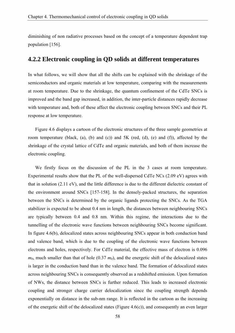
Chapter 4. Thermomechanical control of electronic coupling in QD solids
58
diminishing of non radiative processes based on the concept of a temperature dependent trap
population [156].
4.2.2 Electronic coupling in QD solids at different temperatures
In what follows, we will show that all the shifts can be explained with the shrinkage of the
semiconductors and organic materials at low temperature, comparing with the measurements
at room temperature. Due to the shrinkage, the quantum confinement of the CdTe SNCs is
improved and the band gap increased, in addition, the inter-particle distances rapidly decrease
with temperature and, both of these affect the electronic coupling between SNCs and their PL
response at low temperature.
Figure 4.6 displays a cartoon of the electronic structures of the three sample geometries at
room temperature (black, (a), (b) and (c)) and 5K (red, (d), (e) and (f)), affected by the
shrinkage of the crystal lattice of CdTe and organic materials, and both of them increase the
electronic coupling.
We firstly focus on the discussion of the PL in the 3 cases at room temperature.
Experimental results show that the PL of the well-dispersed CdTe NCs (2.09 eV) agrees with
that in solution (2.11 eV), and the little difference is due to the different dielectric constant of
the environment around SNCs [157-158]. In the densely-packed structures, the separation
between the SNCs is determined by the organic ligands protecting the SNCs. As the TGA
stabilizer is expected to be about 0.4 nm in length, the distances between neighbouring SNCs
are typically between 0.4 and 0.8 nm. Within this regime, the interactions due to the
tunnelling of the electronic wave functions between neighbouring SNCs become significant.
In figure 4.6(b), delocalized states across neighbouring SNCs appear in both conduction band
and valence band, which is due to the coupling of the electronic wave functions between
electrons and holes, respectively. For CdTe material, the effective mass of electron is 0.096
m0, much smaller than that of hole (0.37 m0), and the energetic shift of the delocalized states
is larger in the conduction band than in the valence band. The formation of delocalized states
across neighbouring SNCs is consequently observed as a redshifted emission. Upon formation
of NWs, the distance between SNCs is further reduced. This leads to increased electronic
coupling and stronger charge carrier delocalization since the coupling strength depends
exponentially on distance in the sub-nm range. It is reflected in the cartoon as the increasing
of the energetic shift of the delocalized states (Figure 4.6(c)), and consequently an even larger

4.2 Thermomechanical control of electronic coupling
59
redshift is observed experimentally compared to densely packed SNCs. Förster-type resonant
energy transfer (FRET) is excluded here as a dominant mechanism, since after size selective
precipitation, the SNCs have a very narrow size distribution of about 10%, and FRET
typically does not lead to a shift of the low energy edge of the PL emission [114].
Figure 4. 6: Cartoon representation of the sample geometries studied at 300K and 5K: (a) and (d),
well-dispersed SNCs in a matrix, (b) and (e), densely packed SNCs and (c) and (f), polycrystalline
NW. D and L indicate the size of the NC and the distance between neighbouring SNCs. At 300K, from
(a) to (c), the decrease of the inter-particle distance leads to the increase of exchange interaction and
larger energetic shift of the delocalized states. At 5K, the shrinkage of the crystal leads to the increase
of the band gap of isolate CdTe NCs (d). The decrease of the separation between SNCs in the QD
solids increases the electronic coupling and the energetic shift of the delocalized states (e and f).
We now turn to the PL at 5K. For bulk CdTe, band gap widening at low temperatures is
well-known [94] and has been explained by the shrinkage of the crystal lattice and reduced

Chapter 4. Thermomechanical control of electronic coupling in QD solids
60
phonon scattering [95]. The temperature-induced blueshift of the PL of isolated SNCs in PVA
of 100 meV is similar to the bulk value of 90 meV [159] (Figure 4.6(d)).
The optical and electronic properties of the densely packed SNC film at low temperature
are determined by the shrinkage of the whole system. The shrinkage of CdTe crystal lattice
and the reduction of phonon scattering increase the band gap of CdTe SNCs. In addition, the
shrinkage of the whole system including organic ligands in the SNC film reduces the
separation between SNCs and increases the electronic coupling between them, which partially
compensates the blueshift of the PL caused by isolated SNCs (illustrated in figure 4.6(e)). The
influence of the electronic coupling caused by the shrinkage of SNCs in QD solids is a small
effect and will be neglected here. Comparing with the temperature-induced band gap
widening of isolated CdTe SNCs, the electronic coupling between SNCs in the densely
packed SNC film was still very weak at low temperature, and a temperature-induced blueshift
to 80 meV was experimentally observed in densely packed SNCs.
The redshift of the PL in the NWs at low temperature can be explained using the same
model. In the NWs, the distance between the SNCs is smaller than 0.5 nm. Within this regime,
the electronic coupling increases strongly with the decrease of the separation. At low
temperature, the shrinkage of the organic ligands in the NWs greatly increases the electronic
coupling, and, the energetic shift of the delocalized states caused by the electronic coupling
between neighbouring SNCs overcompensates the temperature-induced band gap widening of
isolated CdTe SNCs, illustrated in the cartoon by comparing figure 4.6(c) and (f). The strong
electronic coupling results in a redshift of the PL spectra in polycrystalline NWs at low
temperature.
4.2.3 Calculation of electronic coupling in QD solids
Theoretical descriptions of electronic coupling between SNCs need to take into account the
quantum-mechanic nature of the SNCs. In QD solids, the wave functions of electrons and
holes are typically obtained by numerically solving Schrödinger’s equation in a chosen
potential such as rectangular or Gaussian confining potentials [160]. The wave functions
generally extend into the classically forbidden regions, which leads to spatial overlap with
wave functions of electrons and holes in neighbouring SNCs when the inter-particle distance
is sufficiently small. The tunnelling of the electronic wave functions eventually results in
energetic degeneracy and delocalization of the states in the QD solids. In addition, Coulomb

4.2 Thermomechanical control of electronic coupling
61
interaction between charge carriers needs to be taken into account. The Coulomb interaction
can be either repulsive, i.e., electron-electron or hole-hole-interaction, or attractive, i.e.,
exciton binding. The latter case, relevant after optical excitation, counteracts the above
discussed delocalization of the charge carriers, while the former case is more relevant in the
description of charge carrier transport [161]. A careful consideration of both tunnelling and
Coulomb interaction is needed for an accurate description and to identify the dominant
mechanism in a given QD solid. We firstly estimate the electronic coupling energy in a simple
tight binding model and then discuss more systematic semiempirical calculations.
Within a simple tight binding model we estimate the electronic coupling energy Eβ
between neighbouring SNCs from the observed decrease of the band gap ∆Eg neglecting the
exciton binding energy [29]. Assuming a (locally) hexagonally close packed arrangement of
SNCs with 12 nearest neighbours so that
ββ EmmEE
h
eg 15)1(12 ≈+=∆ (4.1)
Here we use the approximation that the effective hole mass is four times the effective electron
mass in CdTe [160]. With this, the coupling energy between two neighbouring SNCs at room
temperature is becomes 3 meV in densely packed SNCs and between 4 and 7 meV in NWs.
At 5K these values increase to 5 meV and to the range between 15 and 20 meV, respectively.
In order to obtain a more quantitative estimate of the electronic coupling effects between
SNCs in the NWs we modelled the system by using a semiempirical approach based on an
effective mass approximation [162-163]. The calculation was carried out by C. Mauser. In the
stationary Schrödinger equation ψψ EH = , the exciton-Hamilton is
heheh
he
e rrerUrU
mmH rr
rrhh
−−++∇−∇−=
0
22
*
22
*
2
4)()(
22 πεε (4.2)
The last part is the Coulomb term, the coupling between electron and hole.
If we do not consider the Coulomb interaction, the ground-state wave function and energy
of electron and hole can be obtained by solving the Schrödinger equation of electron and hole
separately. The coupling energy is defined as the energy shift of the lowest conduction and
valence band levels for interacting SNCs compared to a single SNC:

Chapter 4. Thermomechanical control of electronic coupling in QD solids
62
couplingE energy = nglesiE SNC - teractinginE SNCs (4.3)
Here, we use the effective masses of electrons and holes in CdTe NCs 0.096 m0 [101] and
0.37 m0 [102], respectively. As dielectric constant of CdTe 7.1 is used [164], and the potential
barrier between the SNCs was set to 2 eV. The Schrödinger equation was solved for a single
exciton in single SNCs with a diameter of 3.3 nm as reference. And SNC diameters and SNCs
in a hexagonally closed packed geometry with 12 nearest neighbours were calculated with a
dielectric constant for the remaining capping ligands of 3.
Figure 4. 7: (a) and (b) Isosurface-plot of distribution of the electronic wave function in isolated NC
and NC dimer, respectively. (c) Coupling energy between the SNCs in the dimer as function of the
distance.
The distributions of the electron wave function are displayed in a coloured isosurface plot
for a single CdTe NC and NC dimer in figure 4.7 (a) and (b), and the coupling energy of
electrons and holes in the NC dimer at different barrier energy was calculated in figure 4.7(c)
for different distances. It can be seen that for both electrons and holes, the coupling energy

4.2 Thermomechanical control of electronic coupling
63
increases with decreasing distance, and the increase is becoming stronger at smaller distance
(electron coupling increases 7 meV when the inter-particle distance decreases from 0.3 to 0.2
nm, while 5.6 meV when the distance changes from 0.4 to 0.3 nm). Because of the large
effective mass, the coupling between holes is much smaller than electrons.
Figure 4. 8: (a) Geometry of the NC cluster considered here. Isosurface-plot of wave function
distributions of electron (b) and hole (c) calculated using the geometry in (a). (d) Coupling energy
between the SNCs in the cluster as function of the distance between them.
The coupling energy between the CdTe NCs in a NW is calculated for the 12 nearest
neighbours in a hexagonally closed packed geometry. The three-dimensional arrangement of
the SNCs in a hexagonal closed packed system is shown in figure 4.8(a), and the distance
between the SNCs is 0.3 nm. In Figure 4.8(b) and (c), the wave function distributions of the
electron and hole are displayed in a coloured isosurface plot for the same configuration of
figure 4.8(a), respectively. The calculated coupling energy for different distances is illustrated

Chapter 4. Thermomechanical control of electronic coupling in QD solids
64
in figure 4.8(d). It indicates that at sub-nm distances, the coupling energy can shift in the 100
meV range. The energy level shift strongly depends on the inter-particle distance when the
distance between SNCs is very small.
If the Coulomb interaction between electrons and holes is included, the Hamiltons of the
electron and hole can be described by the uncoupled term with an effective potential
)(rU effectiver :
)()(2 ,
2*
2
eeffectiveheeee
e rUrUm
H rrh++∇−= (4.4)
)()(2 ,
2*
2
heffectiveehhhh
h rUrUm
H rrh++∇−= (4.5)
The effective potential is calculated with the Poisson equation
)()( ,/,/ rqrU effectiveheeffectiveherr
Φ⋅= (4.6)
It satisfies
0
2/
0
/,/
2 )()()(
εεψ
εερ rer
r heheeffectivehe
rm
rr
−=−=Φ∇ (4.7)
The Hartree-Fock method was used for the determination of ground-state energy and
wave function. The uncoupled Schrödinger equation of holes ( 0)(, =heffectivee rV r ) was firstly
solved numerically to obtain the ground-state wave function hψ . Using this wave function,
we can determine the effective potential )(, eeffectiveh rU r , which helps us to solve the Schrödinger
equation of electrons. The wave function eψ is used for the effective potential of electrons
)(, heffectivee rV r , which appears in the Schrödinger equation of holes. And then the wave function
of holes can be determined in the second cycle. By iteration, we can determine the stable
eigenvalues (energy) and wave functions of electrons and holes.
Figures 4.9 (a) and (b) show the wave function distributions of hole and electron without
Coulomb interactions. Clearly the wave functions extend to neighbouring CdTe NCs,
indicating the coupling in the NC ensemble. Figure 4.9(c) is the distribution of wave function

4.2 Thermomechanical control of electronic coupling
65
indicating the coupling in the NC ensemble. Figure 4.9(c) is the distribution of wave function
of electron after three cycles of calculation using Hartree-Fock method. Comparing with the
distribution without Coulomb interaction (figure 4.9(b)), Coulomb interaction shrinks the
wave function to the centre, and the strength of coupling decreases. It can be understood,
because Coulomb interaction between electrons and holes is attractive (exciton binding). The
fourth cycle further decreases the tunnelling of the wave function (figure 4.9(d)). After six
cycles, the distributions of the wave function are stable, and we find Coulomb interaction
greatly confines the wave functions of electrons (figure 4.9(e)) and holes (figure 4.9(f)) in the
SNCs.
Figure 4. 9: (a) and (b) Isosurface-plot of wave function distributions of hole and electron without
Coulomb interaction. (c) and (d) Wave function distributions of electron after 3 cycles and 4 cycles of
calculation. (e) and (f) Wave function distributions of electron and hole considering Coulomb
interaction.
Figure 4.10 compares calculations that take into account both Coulomb and tunnelling
coupling (black squares), or tunnelling coupling only (blue circles). It can be observed in
figure 4.9 that Coulomb interaction shrinks the wave function to the centre, and reduces the
coupling strength. In both cases, energy level shifts, in the 100 meV range were found for
sub-nm distances between the CdTe NCs. And the magnitude of the calculated coupling
energies corresponds well to the redshifts observed for individual NWs as compared to well
separated SNCs at room temperature and 5K, respectively. This supports our attribution of the
redshifts to electronic coupling between the SNCs and suggests that we mainly observe
nearest neighbour interactions. Furthermore, it can be seen that the Coulomb interaction

Chapter 4. Thermomechanical control of electronic coupling in QD solids
66
lowers the coupling energies due to higher localization of the charge carriers. However, this
effect is smaller than the tunnelling coupling which therefore governs the coupling energy at
small distances and thus the redshifts. More realistic model need to take into account the
disorder of the SNCs in the NWs and the barrier variation. In conclusion, our simple model
calculations reproduce the order of magnitude of the observed redshifts. It is also revealed
that the electronic coupling is dominated by tunnelling interactions between the nearest
neighbours.
Figure 4. 10: Coupling energy between the SNCs in the cluster as function of the distance between
them without (black squares) and with Coulomb interaction (blue circles).
4.2.4 Composite nature of polycrystalline NWs
Our interpretation that the polycrystalline NWs are composite materials composed of CdTe
SNCs and organic ligands in between is supported by length measurements of individual
NWs by TEM at different temperatures.
The length of individual NWs was measured at room and liquid nitrogen temperatures
using TEM. The measurements were carried out in collaboration with Dr. M. Döblinger and
we observed significant shrinkage between 0.2 and 0.4%. This corresponds to thermal
expansion coefficients (averaged over this temperature range) of 1x10⁻⁵ to 2x10⁻⁵/K.
Polystyrene latex beads (Sigma, LB-11) were also measured at room and liquid nitrogen

4.2 Thermomechanical control of electronic coupling
67
temperatures, and an average shrinkage of 0.9% was observed, corresponding to a thermal
expansion coefficient of 4.5x10⁻⁵, which agrees with that of organic materials (5x10⁻⁵ to 10-
4/K). It shows that the shrinkage values of the polycrystalline NWs are larger than the values
for bulk CdTe (~3x10⁻⁶/K [165]), while smaller than that of organic materials, suggesting that
we observe the behavior of a composite material. An averaged linear expansion coefficient of
the NWs αNW as we have measured can be estimated as
)/()( 111 dDdD SNCSNCCdTeNW ++= ααα (4.8)
where CdTeα and 1α are the expansion coefficients of CdTe and ligands, respectively, and
SNCD and 1d are the SNC diameter and the inter-SNC distance filled with ligands,
correspondingly. Using this equation, the above expansion coefficients, and SNCD =3.3 nm,
we estimate a lower limit for the inter-NC-distances 1d of 0.3 nm, which is an order-of-
magnitude estimate in the expected range. It should be noted that the shrinking of the NWs is
not substrate-induced since the substrates, for both optical and TEM measurements, have
linear expansion coefficients much smaller than observed for the NWs.
Because of the existence of organic ligands in the NWs, low conductivity is expected in
the polycrystalline NWs. In order to measure the conductivity of a singe NW, NWs were
deposited on a quartz substrate, and Au finger electrodes were deposited on top. A single NW
connecting electrodes was observed by optical microscopy shown in figure 4.11(a). Then all
the other electrodes were destroyed, leaving only this pair of electrodes with the single NW
connecting them. The conductivity was measured using Agilent 4156C Semiconductor
Parameter Analyzer by two-terminal sensing. Similar method was used for the measurements
of bare substrate.
Figure 4.11(b) shows I-V cures of a single NW (red) and the quartz substrate (black)
measured in vacuum. A very weak current is observed through the NW. The almost
symmetrical nonlinear I-V curve of the NW exhibits the sign of a Schottky barrier in this
system. The Schottky barrier is a well-studied phenomenon that exists at the metal-
semiconductor interface [166], and it has a direct effect on the nonlinearity of the I-V curve
[167]. At very low bias, the current passing through the system is small and mainly
distributed on the Schottky barriers. At high bias the majority of the voltage drop is
distributed to the NW [167]. Here, the resistance is calculated when the voltage is larger than

Chapter 4. Thermomechanical control of electronic coupling in QD solids
68
6 V. The resistively of the nanowire is about 2×10⁶ Ω·cm, which is two orders larger than that
of polycrystalline CdTe NWs reported by M. C. Kum et al. (~1×10⁴ Ω·cm) [168]. The poor
conductivity in the polycrystalline NWs is due to the composite nature of the NWs. The
existence of the organic ligands prevents the charge transport in the NWs.
Figure 4. 11: (a) Optical image of a single NW connects two electrodes. (b) I-V curve of the NW (red)
and substrate (black).
4.3 Conclusion
In this chapter, we demonstrate a new mechanism to control the electronic coupling in QD
solids. This new mechanism, i.e., thermomechanical control of the electronic coupling, is
realized by controlling the expansion and shrinkage of inter-particle distance by temperature.
Semiempirical calculations of the coupling energies agree well with experiment and it is
revealed the coupling is dominated by tunnelling coupling between the nearest neighbouring
interactions. The QD solids are composed of CdTe SNCs and organic ligands between them.
Three different kinds of samples, isolated CdTe SNCs, densely packed SNC film, and
polycrystalline NWs prepared using the same SNCs were investigated. The increasing
electronic coupling between SNCs due to the decreasing inter-particle distance was
demonstrated by the increasing redshift of the PL spectra in the three samples. At 5K, the
shrinkage of the inter-particle distance allows for an increase of electronic coupling in QD
solids. Comparing with that of isolated SNCs, a smaller blueshift of PL spectra was observed
in densely packed SNC film with weak electronic coupling. A redshift of PL spectra from
CdTe QD solids was firstly observed in polycrystalline NWs with strong electronic coupling.
Coupling energies were calculated for the nearest neighbours in a hexagonally closed packed

4.3 Conclusion
69
geometry. They show the right order of the magnitude comparing with the redshifts observed
for individual NWs at room temperature and 5K, respectively. This supports our attribution of
the redshifts to electronic coupling between the nearest SNCs.

Chapter 4. Thermomechanical control of electronic coupling in QD solids
70

71
5. Optical anisotropy of semiconductor
NWs beyond the electrostatic limit
In the previous chapter, we investigated the electronic coupling between semiconductor
nanocrystals in polycrystalline nanowires, which determines the optical properties of NWs.
Here, we will investigate how light is absorbed/emitted in NWs, and how these processed
depend on the size of the NWs. In particular, polarization anisotropies were observed in
excitation, photoluminescence, and Rayleigh scattering from CdTe NWs with diameters of
about 90 nm. Finite-difference time domain calculations were performed with realistic
parameters of the CdTe NWs for polarized photoluminescence. It is demonstrated that for
NWs with diameter comparable with the wavelength of light in material, the optical
anisotropies are determined by diameter-wavelength ratio, the material dispersion of the NW
(i.e., the wavelength dependency of the refractive index), as well as the local refractive index
of the surrounding. The ensembles of NWs arrays in polymer films were prepared by
stretching the film. The optical anisotropies of individual NWs can be completely transferred
into macroscopically aligned polymer films. The polarization properties of the NW arrays are
not only determined by the optical anisotropies of isolated NWs, but also by the disorder of
the NWs in the film, the local environment and multiple scattering in the thick film.

Chapter 5. Optical anisotropy of semiconductor NWs beyond the electrostatic limit
72
5.1 Optical anisotropies in single NWs
Semiconductor NWs exhibit strong polarization anisotropies of excitation, photoluminescence,
and photoconductivity when the diameter of the NWs is much smaller than the wavelength of
light in the material, i.e., the NW is in electrostatic limit [66]. NWs with diameters
comparable to the wavelength of light in the material might have some interesting properties
that are absent both for very thin NWs and bulk-like materials[136-137]. Here, we will
explore size-dependent optical anisotropies in NWs beyond the electrostatic limit.
The NWs investigated were prepared by the oriented attachment of colloidal CdTe SNCs
as introduced in chapter 3. The absorption (red) and PL (black) spectra of the CdTe NCs used
to prepare the NWs are shown in figure 5.1(a). The absorption at 535 nm indicates the CdTe
NCs have a diameter of 3.1 nm. As an evidence for the formation of NWs, a representative
TEM image of the products is shown in figure 5.1(b). The TEM image shows that the NWs
have an average diameter of about 90 nm. From the analysis of more than 50 NWs, the NWs
have an average diameter of 90 nm with a standard deviation of 20 nm as determined from the
TEM images. This diameter range is on the same order of magnitude as the wavelength of
visible light in, the high refractive index, CdTe. The green curve in figure 5.1(a) is a typical
PL spectrum of an individual NW. Comparing with the photoluminescence of the SNCs in
solution, the spectrum of the NW is redshifted. It indicates the electronic coupling between
the SNCs in the polycrystalline NWs, which is discussed in chapter 4. Here, we want to
explore whether there are size-dependent effects in these NWs.
Figure 5. 1: (a) Absorption (red, triangle) and PL (black, square) spectra of the SNCs used to prepare
the NWs. The green curve (circle) is a typical PL spectrum of a single NW. (b) A TEM image of the
NWs. (c) Statistic distribution of the diameter of NWs.

5.1 Optical anisotropies in single NWs
73
5.1.1 Polarized photoluminescence from single NWs
Polarization anisotropies in excitation and photoluminescence were investigated from
individual NWs. The measurements were performed on a home built single-molecule
spectroscopy setup, which has been introduced in chapter 3. The wavelength of the excitation
was fixed at 415 nm.
Figures 5.2 (a)-(f) show PL images of an individual NW excited with linearly polarized
laser light, the polarization of the excitation is indicated by the arrows in each panel. It can be
clearly seen, that, the PL intensity is smallest when the polarization of the excitation is
perpendicular to the long axis of the NW, and largest when they are parallel with each other.
Figure 5. 2: Polarized photoluminescence in a single NW. (a)-(f) Wide-field PL images of an
individual NW for different excitation polarizations as indicated by the arrow (raw data). The scale bar
is 5µm. (g) and (h) PL intensity under linearly polarized excitation or detection, respectively, of the
same individual NW shown in (a)-(f). The angle is measured with respect to the long axis of the NW.
Squares are experimental data, and curves are best fits to cos²-functions.

Chapter 5. Optical anisotropy of semiconductor NWs beyond the electrostatic limit
74
Figure 5.2(g) quantifies the PL intensity for a larger number of excitation angles. The
angular dependence, like all the following dependences, can be well fitted by cos²-function.
The polarization anisotropy is defined by
⊥
⊥
+−
=IIII
P//
// (5.1)
The anisotropy in excitation for this NW as calculated from the fit parameters is 0.37.
Upon excitation of the same NW with circularly polarized light and a polarizer in the
detection path, the curve displayed in figure 5.2(h) is obtained. The polarization anisotropy of
P = 0.52 for polarized detection is larger than that for the excitation. This observation is the
same for all individual NWs investigated, which shows average polarization anisotropies of
0.32 and 0.48 with standard deviations of 0.10 and 0.07 for polarized excitation and detection
of photoluminescence, respectively.
5.1.2 Breakdown of the electrostatic limit
If we simply consider the electrostatic limit, in which the diameter of the NW is much smaller
than the wavelength in the material, the polarization anisotropies would be explained by the
dielectric contrast between NW and surrounding environment [66]. The incident electric field
eE would not be attenuated inside the NW if the polarization of the excitation is along the
long axis of the NW. But if it is perpendicular to the NW axis, the attenuation of the electric
field would be determined by the dielectric contrast between the NW and the environment,
following the equation
ei EE ⎟⎟⎠
⎞⎜⎜⎝
⎛+
=0
0
)(2
εωεε
(5.2)
Here, Ei and Ee are the electric field inside the NW and the excitation field, respectively. 0ε is
the dielectric constant of the surrounding environment, and )(ωε is the dielectric constant of
the NW.
The polarization ratio defined in equation 5.1 can be written as
200
2
200
2
5)(2)(3)(2)(εεωεωεεεωεωε
++
−+=P (5.3)

5.1 Optical anisotropies in single NWs
75
The dielectric constant of bulk CdTe is between 12 and 9 in the UV-Vis spectral range
[103], and if we neglect the contributions from the substrate, one would expect a polarization
anisotropy larger than 0.9 in excitation. This value of the polarization anisotropy calculated in
the electrostatic limit is much larger than what we observed.
In this simple calculation, we neglect the existence of organic stabilizer in the NWs. We
have demonstrated in the previous chapter that the NWs prepared from SNCs are composite
materials. In order to estimate the effect of the composite materials on the dielectric constant,
we assume that the CdTe NCs in the NWs are closely packed and occupy 74% of its volume.
The composite nature of the NW was taken into account by estimating its effective dielectric
constant using the Maxwell-Garnett approximation [169-170]
)1()2()22()21(
δεδεδεδε
εε−++
−−+=
im
mime (5.4)
Here, eε is the effective dielectric constant of the medium, iε is the dielectric constant of the
inclusions and mε is that of the matrix. δ is the volume fraction of the embedded material. In
the polycrystalline NWs, the CdTe SNCs are treated as the matrix. If we assume the dielectric
constant of CdTe is 9, and that of TGA ligands is 2, then the NWs have an effective dielectric
constant of 6.7. The polarization ratio of this material calculated in the electrostatic limit is
0.87, which is still much larger than the experimental results.
It should also be noted that in the electrostatic limit, the polarization anisotropy is
determined by the dielectric constant, which depends on the wavelength in the material. D. T.
F. Marple measured the refractive index of several materials at 300K from a prism of melt-
grown material with polished surfaces [171]. The following empirical formula was found for
the dielectric constant:
22
2
)(c
BA−
+=λ
λλε (5.5)
For CdTe, the best values of the parameters are A = 5.68, B = 1.53, and c2 = 0.366. This shows
that the dielectric constant decreases with increasing wavelength. So compared to polarized
detection, the polarized excitation has higher dielectric constant since it occurs at shorter
wavelength. According to equation 5.3, the optical anisotropy of polarized excitation should

Chapter 5. Optical anisotropy of semiconductor NWs beyond the electrostatic limit
76
be larger than that of polarized detection. However, our measurements show an opposite
effect: the polarization ratio of detection was observed to be larger than that of excitation for
all individual NWs.
Both of these phenomena strongly suggest that the polarization anisotropies reported
above reflect the breakdown of the electrostatic limit. For a proper explanation, the finite NW
diameter needs to be taken into account.
5.1.3 FDTD calculations of polarization anisotropies
In order to have a full understanding of the polarization of the NWs with diameter comparable
to the wavelength of the light in the semiconductor material, a series of FDTD calculations
were performed to include a finite NW diameter. The calculations were carried out by A. A.
Lutich. In the calculations, the NW was modeled as a cylinder placed on a silica substrate
( subε = 2.13). The cylinder has an effective dielectric constant effε and a diameter d. With
bulk dielectric constants for different wavelength from the literature, we considered the
composite nature of the NWs and found the effective dielectric constant at 400 nm and 600
nm are 8.3 and 6.42, respectively [103]. Both of these effective dielectric constants predict
polarization anisotropies larger than 0.8 in the electrostatic approximation, and thus
significantly larger values than what we observed in the measurements.
The simulated geometries are illustrated in figure 5.3 (a) and (c) for the excitation and
detection of photoluminescence, respectively. For the polarization anisotropy in excitation,
the NW was excited by an incident plane wave at 400 nm, which is close to the experimental
excitation wavelength (415 nm). The polarization anisotropy was determined by comparing
the average power density in the NW when the polarization of the incident plane wave was
parallel or perpendicular to the long NW axis, respectively. For the calculation of the
polarization anisotropy in detection, a point source was placed inside the NW with its dipole
moment parallel to the substrate. The emission was set to 600 nm, which is close to the
emission of the NWs. The polarization anisotropy was calculated from the energy flux
passing through the plane of a virtual detector in the far-field when the dipole moment was
either parallel or perpendicular to the NW axis, respectively. In the latter approach we did not
include the anisotropy in excitation because we found that ensembles of SNCs immobilized
on a substrate did not exhibit a polarized emission under linearly polarized excitation.

5.1 Optical anisotropies in single NWs
77
Figure 5. 3: (a) and (c) Simulated geometries for the excitation and detection of PL, respectively. (b)
and (d) Calculated polarization anisotropy in excitation and emission as function of the NW diameter-
to-vacuum wavelength ratio, respectively. The blue curves represent the calculation using electrostatic
limit without a substrate, the red solid curves show FDTD calculations including the substrate, and the
black dash-dot curves are FDTD calculations without the substrate.
The results of the calculations are summarized in figure 5.3 (b) and (d). Figure 5.3(b)
displays the calculated polarization anisotropies in excitation as function of diameter-
wavelength ratio d/λ of the NW. The blue line represents the calculation using the dielectric
contrast model. The black dash-dot curve represents our calculation in absence of the
substrate, while the red solid curve is the calculation including the substrate. Firstly, we point
out that at the smallest ratios, i.e., thinnest NWs, our calculations without substrate perfectly
reproduce the electrostatic limit and predict a polarization anisotropy of 0.9. The presence of
the substrate (red curve) lowers this anisotropy slightly since the refractive index “contrast”
near the NW is reduced. However, at d/λ ratios larger than 0.05, significant deviation from the

Chapter 5. Optical anisotropy of semiconductor NWs beyond the electrostatic limit
78
electrostatic limit are observed. First, the anisotropy slightly increases, and then, at ratios
exceeding 0.1 sharply decreases, displaying a strong diameter dependence. For NWs with a
diameter of 90 nm and an excitation wavelength of 400 nm our calculations predict a
polarization anisotropy of ~0.38, which is in excellent agreement with the observation of
0.32+/-0.1 for individual NWs reported above. We therefore conclude that the observed
polarization anisotropies reflect the finite diameter of the NWs and thus the breakdown of the
electrostatic limit associated with it.
Figure 5.3(d) displays the calculation results for the polarization anisotropy in the
emission. Qualitatively, the same behaviour, i.e., agreement with the electrostatic limit at
small d/λ ratios and sharp decrease of polarization at large d/λ ratios, is observed. Subtle but
important difference can be found: Both the electrostatic limit and our calculation now predict
slightly lower polarization anisotropies for the thinnest NWs, compared to the polarized
excitation. According to equation 5.5, the dielectric constant at the detection wavelength is
smaller than that for the excitation, and a smaller polarization ratio is expected in the
polarized detection.
The predicted difference of the polarization anisotropy in emission and excitation is
further illustrated in figure 5.4, in which we show excem PPP −=∆ as function of the d/λ ratio.
Two facts should be noted: Firstly, one can see that at small d/λ ratios, excP is larger, which
agrees with the argument of dielectric contrast model, while for larger d/λ ratios, emP is larger.
Secondly, the largest diameter dependent differences are observed in the diameter range
spanned by our NWs. For thin NWs, our calculations reproduce the polarization of
electrostatic limit, indicating the polarization ratio is determined mainly by the dielectric
contrast as discussed above. The effective dielectric constant of CdTe at excitation
wavelength (400 nm) is larger than that at detection wavelength (600 nm). And the higher
polarization in the excitation is due to the larger dielectric contract between the NW and the
environment. While for NWs with diameter-wavelength ratio larger than 0.1, for both the
excitation and detection, the polarization ratio drops very fast when increasing the d/λ ratio of
the NWs. For the same NW, the diameter-wavelength ratio is smaller at the detection
wavelength than that for excitation. Thus, the calculations predict a larger polarization
anisotropy of NWs in detection than in excitation. In a word, the polarization competition
between the excitation and the emission depends both on the material dispersion and the

5.1 Optical anisotropies in single NWs
79
diameter-wavelength ratio. The diameter of the NWs investigated in the thesis lies in the
region where the polarization is mainly determined by the diameter-wavelength ratio, and
experimentally, we observed that individual NWs show (on average) 50% higher anisotropies
in the emission.
Figure 5. 4: The difference of the polarization anisotropy between detection and excitation.
5.1.4 Polarized scattering from single NWs
The NWs beyond electrostatic limit show strong Rayleigh scattering when excited by white
light in a dark-field microscope. The Rayleigh scattering of single NWs shows a polarization
anisotropy in excitation and emission when a polarizer is placed in either the excitation path
or in front of the detector.
Figures 5.5(a) through (l) show scattering images of two individual NWs excited with
non-polarized white light and detection at different polarizations. The polarization of the
detection is indicated by the arrows. Similar to the PL, the scattering of the NWs also shows
polarization anisotropies. Quantified scattering intensities in excitation and detection from the
NW marked by the arrow were plotted in figures 5.5(m) and (n), respectively. The red curves,
fits by cos²-function, indicate polarization anisotropies of 0.34 and 0.61 for scattering
excitation and detection, respectively. The measurements of a number of NWs yield average
values of 0.58 and 0.35, with standard deviations of 0.06 and 0.04, for polarized detection and
excitation of scattering, respectively. Similar to the case of PL, the anisotropy is larger for the
polarized detection.

Chapter 5. Optical anisotropy of semiconductor NWs beyond the electrostatic limit
80
Figure 5. 5: Polarized scattering in single NWs. (a)-(l) Rayleigh scattering images of two individual
NWs when excited by non-polarized light and detected at different polarizations. The height of the
images is 60µm. (m) and (n) Rayleigh scattering intensity of the NW marked by the arrow under
polarized excitation and detection, respectively. The angle is measured with respect to the long axis of
the measured NW. Squares are experimental data, and curves are best fits to cos²-functions.
The polarization anisotropies in Rayleigh scattering are more complicated than in
photoluminescence, and we limit ourselves to a qualitative discussion here. One can expect an
anisotropic excitation of classical scattering dipoles, and these classical scattering dipoles will
lead to anisotropic scattering. The calculations for the polarization anisotropy in excitation of
photoluminescence can in principal also be used for the classical scattering dipoles. However,
the polarized excitation and detection in scattering is performed in the same, much broader
spectral range, so the above discussion on material dispersion and wavelength are not valid
anymore. In addition, with a polarizer in front of the dark field condenser the excitation
polarization at the sample is not purely linearly polarized [172]. The polarization of the light
will be changed after passing through the dark field condenser, and the light beam only has a
dominant polarization component in the projection of the excitation light into the sample
plane. Therefore, the observed lower polarization anisotropy in excitation is likely to contain
a major component from this difference in excitation geometry.

5.2 Optical anisotropies in NW arrays
81
5.2 Optical anisotropies in NW arrays
Single NWs show optical anisotropies in photoluminescence and scattering, and transferring
the anisotropies into NW arrays is attractive for application as polarized light source, or for
the detection of polarized light [73-74].
The NWs were mixed with PVA and they were aligned by stretching the polymer film.
The process of this method and a typical Rayleigh scattering image of the NW arrays were
shown in chapter 3. As prepared NW arrays have lateral sizes of about 1.5 cm and thicknesses
of about 50 µm.
Figure 5. 6: PL intensity of NW ensembles aligned in polymer films under: (a) under linearly
polarized excitation, and (b) linearly polarized detection. (c) and (d) Rayleigh scattering of these films
with a polarizer in the excitation and detection paths, respectively. Blue squares are experimental data,
and red curves are best fits to sin²-functions.
Rayleigh scattering and photoluminescence of the NW arrays were measured in a
combined dark-field/laser microscopy. The PL of NW arrays was excited with the second
harmonic of a diode-pumped Nd:YAG laser at 532 nm, and Rayleigh scattering was excited
with white light. Polarized excitation and detection were observed in both photoluminescence
and scattering as shown in figure 5.6. The blue squares are experimental data, and red curves

Chapter 5. Optical anisotropy of semiconductor NWs beyond the electrostatic limit
82
are best fits to sin²-functions. The measurements show the polarization ratios for the NW
arrays are 0.22, 0.2, 0.41 and 0.26 for PL excitation, PL detection, excitation and detection of
scattering, respectively. The pronounced optical anisotropies of NW arrays originate from the
contribution of their unit. However, the polarization anisotropies of the NW ensembles are
lower than those of single NWs.
The polarization of single NWs, the disorder of the NWs in the aligned films, the presence
of a higher refractive index environment, i.e., the PVA matrix, as well as multiple scattering
events need to be taken into account to understand the optical anisotropies of the NW arrays.
We will discuss each contribution separately in what follows.
5.2.1 Disorder in NW arrays
In this section, we will discuss the relationship of the optical anisotropies between single
NWs and NW arrays, based on the statistics of the anisotropies in single NWs and the
disorder of the NWs in the NW arrays.
Figure 5.7 shows the distribution of the angle between NWs with respect to the alignment
direction determined from 120 NWs in the scattering image in figure 3.8. The standard
deviation of this distribution is ~30°. The distribution was fitted to a Gaussian distribution
shown by the blue curve.
Figure 5. 7: Distribution of the angle between the long axis of individual NWs and the alignment
direction in the PVA film. The blue curve is the Gaussian fit of the distribution.
Figures 5.8 (a) through (d) display best fits curves of the experimental measurements of
polarized NW arrays (red). Green curves are the calculations from single NWs, considering
the disorder of the NWs in the NW arrays. These curves were obtained from numerically
convoluting the trace expected from an average individual NW with the fitted Gaussian

5.2 Optical anisotropies in NW arrays
83
distribution shown in figure 5.7. The shaded areas represent the standard deviation of the
polarization anisotropies observed for individual NWs.
Figure 5. 8: Polarized PL and Rayleigh scattering in excitation and detection from NW arrays. Red
curves are best fits of the measurements of NW arrays to cos²-functions, and green curves are the
expected polarization anisotropies based on average single NW polarization anisotropy convoluted
with the distribution of the angle shown by the blue curve in figure 5.7. The shaded areas represent
expected standard deviation based on average single NW data.
For the polarization anisotropy in PL excitation and in both excitation and detection of
Rayleigh scattering, we find agreement between the curves calculated from the single-NW
data and the experimental data of the ensembles within one standard deviation. The
polarization anisotropy in PL emission is slightly smaller for the ensembles than expected
from the convoluted single-NW data.
This good agreement, only considering the disorder in the films is surprising, since we did
not consider the presence of the PVA matrix. In what follows, we will discuss the
contribution of the polymer matrix to the optical anisotropy of NW arrays.

Chapter 5. Optical anisotropy of semiconductor NWs beyond the electrostatic limit
84
5.2.2 Polymer environment
The polymer matrix is expected to reduce the “refractive index contrast” with the NWs due
to its refractive index being larger than 1. This should lead to a further decrease of the
polarization anisotropy. We therefore tested the significance of the matrix effect by Rayleigh
scattering from single NWs with a polarizer in the detection path. For the same individual
NWs we obtained polarization anisotropies in air and in PVA film, respectively (figure 5.9).
Indeed, we found that for each NW the polarization anisotropy was significantly reduced in
the higher refractive index medium. On average a reduction of 40% was observed. Similar
behaviour was observed when measuring polarization anisotropies of NWs in air and in oil
with a large refractive index of 1.518.
Figure 5. 9: (a) and (b) Rayleigh scattering intensity of the same NW under polarized detection
measured in air and in PVA film, respectively. Squares indicate experimental data, and curves are best
fits to sin²-functions.
The optical anisotropies of NWs decrease in PVA matrix so large that the agreement by
only considering the disorder in the film must be considered coincidental. Then the in the
films is broken down. Therefore, there must be an additional effect that increases the
polarization ratio in the NW arrays.
5.2.3 Multiple scattering
Since the films are tens of micrometers thick, multiple scattering becomes significant when
light passing through the film. During the multiple scattering processes, the NWs are
illuminated not by circularly polarized light, but by partially polarized light with preferred
polarization ratio long the NW axis, and each of the multiple scattering process increases the
polarization anisotropy of the detected light. An alternative explanation for increased

5.3 Conclusion
85
polarization anisotropy via the birefringence of stretched PVA films is considered unlikely
since the differences in refractive index for the different polarization are small, typically on
the order of 10-2 refractive index units [173].
We therefore attribute the polarization anisotropies in the polymer films to a combined
effect of disorder, higher refractive index matrix, and multiple scattering. The disorder in the
NW arrays and the polymer environment decrease the polarization anisotropies, while the
multiple scattering increases the anisotropies.
5.3 Conclusion
In this chapter, we studied the optical anisotropies in semiconductor NWs as function of the
size of the NWs. The optical anisotropies of individual NWs could be completely transferred
into macroscopically aligned NW arrays. The polarization anisotropy in excitation and
emission of photoluminescence as well as Rayleigh scattering from individual and ensembles
of CdTe NWs aligned in polymer films were investigated. The experimental results on the
photoluminescence of single NWs reflect the breakdown of electrostatic limit, which is used
to explain the optical anisotropies in NWs with diameter much smaller than the wavelength.
FDTD calculations were carried out to understand the anisotropies in the NWs, and the
calculations agree well with the experimental results. It indicates that for very thin NWs, the
anisotropies are mainly determined by the dielectric mismatch between the NW and the
surrounding environment. While for NWs with diameter comparable with the wavelength, the
optical anisotropies strongly depend on the diameter-wavelength ratio of the NWs. We
investigated a NW diameter regime in which a pronounced dependence of the polarization
anisotropy on the diameter-wavelength ratio is observed. In this regime, the optical
anisotropies can be tuned between its maximum predicted by the electrostatic limit to zero. A
lower polarization anisotropy in excitation is observed than in emission because of the higher
diameter-wavelength ratio at shorter wavelength for the same NW. Furthermore, the
polarization anisotropy is affected by the material dispersion of the NWs and the local
refractive index of the environment. The properties of individual NWs can be completely
transferred into macroscopically aligned polymer films. The optical anisotropies of the NW
arrays are determined by the polarization of single NWs, the disorder of the NWs in the
aligned films, the presence of a higher refractive index matrix, as well as multiple scattering

Chapter 5. Optical anisotropy of semiconductor NWs beyond the electrostatic limit
86
events in the thick film. The alignment of the NW arrays opens opportunities for their
applications in polarization sensitive applications.

87
6. Nanoribbon waveguide
In the last chapter, we investigated the absorption, emission and scattering of light by the
one-dimensional nanostructure. Optical anisotropies were observed because of the dielectric
screening of the electric field. Here, we will investigate the propagation of light in the
nanostructures. The nanoribbons prepared from semiconductor nanocrystals serve as optical
waveguide on the nanoscale. When the nanoribbons are optically excited, the
photoluminescence will couple into a guided mode, propagate in the ribbon, and be emitted
at the ends. Calculation and SEM measurements show that most of the nanoribbons are
single-mode waveguides. In addition, coupling between different nanoribbon waveguides is
observed. Re-absorption of the photoluminescence is demonstrated when PL propagating in
the waveguides. The propagation loss of the waveguides is quantitatively determined.

Chapter 6. Nanoribbon waveguide
88
6.1 Nanoribbons prepared by CdTe nanocrystals
The preparation of nanoribbon by the oriented attachment of CdTe NCs was introduced in
chapter 3. The absorption (black) and photoluminescence (PL, red) spectra of the SNCs used
to prepare the nanoribbons are shown in figure 6.1(a). The SNCs have an average diameter of
3.5 nm. The green curve in figure 6.1(a) is the PL spectrum of a single nanoribbon collected
from the whole ribbon. The redshift of the PL spectrum comparing to that of the SNCs is due
to the electronic coupling between the SNCs in the nanoribbons, as discussed in chapter 4.
Figure 6.1(b) shows a TEM image of the nanoribbons. Besides nanoribbons, there are also
some particle chains in the TEM image. The particle chains, as the intermediate products,
were also observed during the preparation of nanowires using NCs [55]. Most of the
nanoribbons have width between 150 and 500 nm, but nanoribbons with diameters of about
100 nm or even thinner were also observed in the TEM and SEM measurements.
Figure 6. 1: (a) Absorption (black) and PL (red) spectra of CdTe NCs with a diameter of 3.5 nm used
to prepare the nanoribbons and a typical PL spectrum of a single ribbon (green). (b) TEM image of
nanoribbons.
6.2 Nanoribbon waveguides
In this section, we will demonstrate that nanoribbons can serve as waveguide, and the PL can
be guided in the nanoribbon and emitted at the tips.
We first measure the PL of the nanoribbon when exciting it locally in the centre. The
experiment was carried out on a dark field microscopy combined with a green laser as

6.2 Nanoribbon waveguides
89
introduced in chapter 3. The experimental geometry is shown in figure 6.2(a). The second
harmonic of diode-pumped Nd:YAG laser at 532 nm was focused by a 100x objective to a
spot less than 1 µm in diameter. The laser spot is much smaller than the length of the
nanoribbons, so the nanoribbons can be excited locally. The scattering or photoluminescence
was collected by the same objective. The nanoribbons were spread on an ITO substrate with
grids prepared using lithography for both morphology and optical investigation. The width of
the nanoribbons was measured using SEM. Figure 6.2(b) and (c) show SEM and scattering
images of the same nanoribbon, respectively. When the nanoribbon was excited in its centre,
pronounced emission was observed at the tips, where the nanoribbon was not excited
(Figure6.2 (d)). It indicates the strong emission at the tips propagated from the middle of the
nanoribbon.
Figure 6. 2: (a) Experimental geometry whereby the nanoribbon is excited in the middle by a focused
laser. (b) SEM image of a single nanoribbon. (c) Scattering image of the same ribbon shown in 2(b).
(d) PL image of the nanoribbon when excited in the middle of the nanoribbon.
The propagation of the signal from the excitation spot to the tips may have different forms.
The excitons might firstly recombine radiatively and the photons then propagate in the
nanoribbon, or the excitons diffuse and emit photons after relaxation into low energy sites
[174]. If it is the diffusion of excitons, strong emission along the whole nanoribbon is

Chapter 6. Nanoribbon waveguide
90
expected. So it is the propagation of PL in the nanoribbon and the photons are emitted at the
tips.
The waveguide behaviour was also observed when the whole nanoribbon was excited.
The measurement is schematically shown in figure 6.3(a). Blue light at 400 nm was focused
using a 100x objective to form an excitation spot of about 50 µm in diameter. This spot is
much larger than the length of the nanoribbons (~ 5 µm), so the whole nanoribbon is excited.
Photoluminescence from the individual ribbons was collected by the same objective and a
CCD was used for imaging. A photoluminescence image of a nanoribbon is shown in figure
6.3(b). Pronounced emission is observed at two spots. The distance between the two spots is
about 5 µm, which is very close to the length of the nanoribbons. So it is expected that the
pronounced emission is from the tips, while the emission from the body of the ribbon is very
weak. It also indicates that the emission from the body is guided in the nanoribbon waveguide
and emitted at the tips.
Figure 6. 3: (a) Experimental geometry whereby the nanoribbon is uniformly excited perpendicular to
its long axis. (b) PL image of a nanoribbon under uniform laser illumination. Scale bar, 5 µm.
6.3 Single-mode nanoribbon waveguides
The development of nanoscale waveguides is an important step towards the manipulation of
optical signals [85-87, 140, 144, 175-177] as discussed in detail in chapter 2. During our
experiments, we found that not all the nanoribbons serve as waveguide. For some
nanoribbons, when they were excited in the centre, emission was only observed at the
excitation position. In order to determine the size of the waveguides, nanoribbons were
dispersed on the ITO substrate with grids on the surface. The nanoribbons were firstly
measured on the dark field microscopy combined with a green laser, and the sizes of the same
ribbons were measured using SEM. Figure 6.4 (a) and (b) show the scattering and SEM
images of the nanoribbons in the same grid. The width distribution of many nanoribbons that
can serve as waveguide is show in figure 6.4(c). The smallest width of nanoribbon waveguide
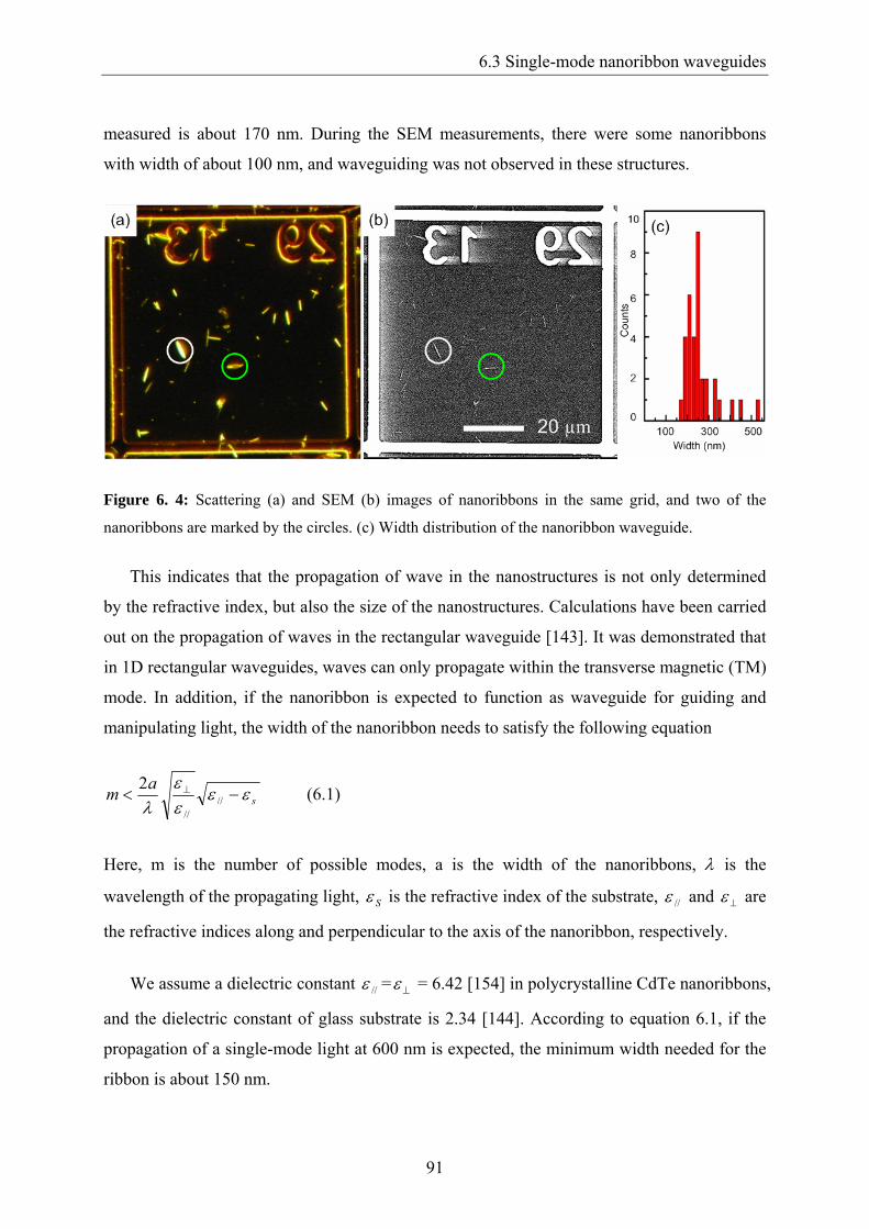
6.3 Single-mode nanoribbon waveguides
91
measured is about 170 nm. During the SEM measurements, there were some nanoribbons
with width of about 100 nm, and waveguiding was not observed in these structures.
Figure 6. 4: Scattering (a) and SEM (b) images of nanoribbons in the same grid, and two of the
nanoribbons are marked by the circles. (c) Width distribution of the nanoribbon waveguide.
This indicates that the propagation of wave in the nanostructures is not only determined
by the refractive index, but also the size of the nanostructures. Calculations have been carried
out on the propagation of waves in the rectangular waveguide [143]. It was demonstrated that
in 1D rectangular waveguides, waves can only propagate within the transverse magnetic (TM)
mode. In addition, if the nanoribbon is expected to function as waveguide for guiding and
manipulating light, the width of the nanoribbon needs to satisfy the following equation
sam εε
εε
λ−< ⊥
////
2 (6.1)
Here, m is the number of possible modes, a is the width of the nanoribbons, λ is the
wavelength of the propagating light, Sε is the refractive index of the substrate, //ε and ⊥ε are
the refractive indices along and perpendicular to the axis of the nanoribbon, respectively.
We assume a dielectric constant //ε = ⊥ε = 6.42 [154] in polycrystalline CdTe nanoribbons,
and the dielectric constant of glass substrate is 2.34 [144]. According to equation 6.1, if the
propagation of a single-mode light at 600 nm is expected, the minimum width needed for the
ribbon is about 150 nm.

Chapter 6. Nanoribbon waveguide
92
This calculation agrees well with our measurements, in which waveguide is only observed
in nanoribbons with width larger than 170 nm. Most of the nanoribbon waveguides have a
width between 180 and 280 nm, and they are expected to be single-mode waveguides. And
for the NWs investigated in the last two chapters, the diameter is not large enough to serve as
waveguide, and the photoluminescence was observes uniform along the NWs.
6.4 Optical coupling between crossed nanoribbons
For the application of waveguide in integrated photonics, it is very important to route the
wave in designed path. In the following experiment, we will demonstrate that the
photoluminescence can not only propagate in isolated nanoribbon waveguides, but can also
couple between crossed ribbons and propagate in another waveguides.
Figure 6. 5: (a) Scattering image of several crossed nanoribbons. (b) Scattering image of the ribbons
with laser spot. (c) PL image of the nanoribbons when excited in the middle of the ribbon 1.
The crossed nanoribbons were prepared by dispersing nanoribbons with high
concentration on the substrate. Figure 6.5(a) shows the scattering image of three crossed
nanoribbons. Here, we only excite ribbon 1 and detect the signal from the crossed ribbons. In
the scattering image shown in figure 6.5(b), we can see the laser spot which is focused on the
middle of ribbon 1. Figure 6.5(c) is the corresponding photoluminescence image. Emission is
observed not only from ribbon 1 which was excited, but also in the other nanoribbons. And
the strongest emission is observed at the crossing of the nanoribbons. The emission at the tips
of ribbon 1 is very weak, while for ribbon 2 and 3, the signal at the ends is stronger than in the
body. It indicates that the photoluminescence produced in the middle of ribbon 1 firstly
propagates along the ribbon, when the wave reaches the crosses between nanoribbons, it tends
to couple to the other ribbon. There is a significant loss when the wave couples between
nanoribbons. The wave coupled into the other ribbon will propagate and be emitted at the tips.

6.5 Losses studied by measuring the PL at tips as a function of excitation position
93
6.5 Losses studied by measuring the PL at tips as a
function of excitation position
The propagation loss is an important parameter in waveguiding. In this section, we will
determine the propagation loss of the nanoribbon waveguides quantitatively.
The scattering image of a typical nanoribbon is shown in figure 6.6(a), and figures 6.6(b)-
(d) show PL images of the nanoribbon when the excitation spot is shifted from left to right,
indicated by the green arrows. The PL spectra at the tips of the ribbon are shown in figures
6.6(e)-(g) for different excitation positions and the black and red curves indicate the emission
spectra at tip 1 and tip 2, respectively.
When the ribbon was excited close to the tip 1 (figure 6.6(b) and (e)), the strong emission
at tip 1 was observed, and the peak position was at 610 nm. At tip 2, very weak emission was
also observed with the emission peak at 616 nm. It should be noted that the emission at both
tips originated from the same source. The spectra in figure 6.6(e) were normalized separately
and shown in figure 6.6(h). One can clearly see that the two curves overlap at the red edge,
i.e., at the edge of the larger wavelength. However, at the green edge with higher energy, the
spectrum of tip 2, which is farther away from the excitation, the spectrum is partially
disappearing. As shown in figure 6.1(a), the spectra of absorption and PL overlap in the green
edge of the PL. Emitted photons with energy lying in the overlap region can be absorbed
when propagating in the nanoribbon. The stronger re-absorption with longer propagation
distance could explain the difference in the normalized spectra very well. The same behaviour
was observed when reversing the tips (figure 6.6(d), (g) and (i)).

Chapter 6. Nanoribbon waveguide
94
Figure 6. 6: (a) Scattering image of a single nanoribbon. (b)-(d) PL images of the nanoribbon in (a)
when excited at different positions, the excitation spots are pointed by the arrows. (e)-(g) PL spectra
collected at the tips of the nanoribbon in (b)-(d), respectively. The black curves are the spectra at tip 1,
and red at tip 2. (h) and (i) are normalized spectra of (e) and (g), respectively.
When the excitation spot was shifted from one end to the other, the redshift of the spectra
at tip 1 was observed from 610 nm to 614 nm and further to 617 nm with the excitation
moving away. In addition, the blue-shift of the spectra at tip 2 was observed from 616 nm to
613 nm and further to 609 nm with the excitation moving closer (figures 6.6(e), (f) and (g)).
The PL images indicate the decreasing of relative intensity with an increasing propagation
distance and stronger re-absorption.

Chapter 6. Nanoribbon waveguide
95
Figure 6. 7: (a)-(g) PL images of a nanoribbon excited with the excitation spots moving from tip a to
tip b . (h) Schematic indication of waves will be emitted at the boundary (red) and waves might
propagate in a nanoribbon waveguide (blue). (i) Schematic depiction of the emission in a waveguide.
The green spots in (h) and (i) indicate the excitation spots. (j) Distance dependence of the out-couple
efficiency at two tips. The red and blue curves are fitted curves.
The loss of the photoluminescence in the nanoribbon waveguide arises from re-absorption,
the disorder induced scattering, etc. To understand the loss in the nanoribbon waveguide
quantitatively, we measured the intensity at the tips as a function of the excitation position.
Figures 6.7(a)-(g) are the PL images of the same nanoribbon when the excitation spot was
moved from one tip to the other. In order to suppress the variation in excitation or emission
efficiency along the waveguide, the PL intensities at a tip are normalized by the emission of
the whole nanoribbon, which is called out-coupling efficiency at this tip.
The total internal reflection at the boundary of a material and the air occurs when the
incidence angle satisfies

Chapter 6. Nanoribbon waveguide
96
1sin ≥θn (6.2)
Here, n is the refractive index of the material. Only the waves satisfying equation (6.2) might
propagate in the nanoribbon waveguide (blue in figure 6.7(h)). Otherwise, they will be
emitted to the air during propagation (red in figure 6.7(h)).
To explain the process, a simple model schematically shown in figure 6.7(i) can be used.
We assume that the nanoribbon waveguide is excited in position S , and the emitted photons
have total intensity of 0I . The waves that do not satisfy equation (6.2) will escape the
nanoribbon and will be emitted at the excitation position with an intensity of 0Iα . Waves with
the same intensity 0Iβ satisfying (6.2) will propagate towards the tip a and b of the
waveguide. α and β fulfil:
12 =+ βα (6.3)
In the following, we assume that the loss of PL is uniform along the axis of the
nanoribbon waveguide. As illustrated in figure 6.7(i), the distances from the excitation
position to tip a and tip b are 1L and 2L , respectively. The length of the nanoribbon
waveguide is
21 LLL += (6.4)
The length of the nanoribbon shown in figure 6.7 is 5.29 µm.
The intensities of the emission at the tip a and b can be expressed by
10
kLa eII −= β , and 2
0kL
b eII −= β (6.5)
Here, k is a fitting parameter.
Then the out-coupling efficiency at tip a is
)2(1 )(00
011
1
21
1
−++=
++=
++= −−−
−
−−
−
LLkkL
kL
kLo
kL
kL
boa
aa ee
eeIIeI
eIIII
Ie
ββ
βαββ
α (6.6)

6.6 Conclusion
97
The out-coupling efficiency at tip a (indicated in figure 6.7(a)) as a function of excitation
distance is plotted in figure 6.7(j) by the red dots. The red curve which fits to equation (6.6)
indicates propagation loss of about 4.2 dB µm-1. The fitted parameter β is 0.435, which
indicates that more than 85% of the wave propagates towards the ends. If we assume that the
nanoribbons have a refractive index of 3 [103], then the θ satisfying equation (6.2) is smaller
than 20°. Similar analysis was carried out on the emission at the other tip, shown in blue in
figure 6.7(j). The fitted parameters of propagation loss and β are 3.6 dB µm-1 and 0.47,
respectively. The propagation loss is in the same order as metallic plasmon waveguides (~1
dB µm-1) [178].
6.6 Conclusion
In this chapter, we demonstrated that nanoribbons prepared by the oriented attachment of
SNCs can serve as single-mode waveguides, and the loss in the nanoribbon waveguides was
quantitatively determined. Strong emission was observed at the ends of the nanoribbons when
they were locally excited. PL investigation shows that the strong emission at the tips arises
from the propagation of PL in the nanoribbon. In addition, the PL was observed to couple
between crossed nanoribbons. SEM measurements show that most of the nanoribbons have a
width between 180 and 280 nm. Calculation indicates these nanoribbons are single-mode
waveguides. Re-absorption was demonstrated when PL propagating in the nanoribbon
waveguides. Propagation loss in the nanoribbon waveguides was studied by measuring the
out-coupling efficiency of the PL at the ends as a function of excitation distance. Results
show that the nanoribbon waveguides have the same order of propagation loss as metallic
plasmon waveguides.

Chapter 6. Nanoribbon waveguide
98

99
7. Conclusions and outlook
This work aims at exploring the possibilities to control the electronic coupling in quantum dot
solids, and to study the size dependent optical properties in quasi one-dimensional
semiconductor nanostructures.
We firstly demonstrated that the electronic coupling in QD solids can be controlled by a
new thermomechanical mechanism. The interstitial material in the QD solids allows control
of the expansion and shrinkage of the solid with temperature, and this thermomechanical
control of the electronic coupling is realized by controlling the inter-particle distance with
temperature. Photoluminescence and TEM investigation demonstrate tuning of the band gap
emission in single polycrystalline nanowires and densely packed semiconductor nanocrystals
via this mechanism. Temperature-induced blueshift in densely packed SNC film and redshift
in polycrystalline NWs were realized at low temperature. The change of PL of QD solids at
low temperature is qualitatively different from that of the bulk material and isolated CdTe
SNCs. The electronic coupling between neighbouring SNCs in the polycrystalline NWs is
estimated to be between 4 and 7 meV at room temperature and between 15 and 20 meV at 5K.
Calculations of the electronic coupling between nearest SNCs for sub-nm distances show the
same order of energetic shift of the delocalized states. This supports our attribution of the PL
shifts to electronic coupling between the nearest SNCs.
Size dependence of optical anisotropies in NWs was demonstrated, and the optical
anisotropies can be transferred into macroscopically aligned NW arrays. Optical anisotropies
in excitation and detection of photoluminescence and scattering were observed in NWs with
diameters of about 90 nm. This diameter range is on the same order of magnitude as the
wavelength of visible light in CdTe. The anisotropies in the thick NWs do not agree with the
calculations of NWs in electrostatic limit. Finite-difference time domain calculations with

Chapter 7. Conclusions and outlook
100
realistic parameters for the CdTe NWs for excitation and photoluminescence anisotropy were
carried out in order to explain the observed anisotropies. It is found that the optical
anisotropies of NWs display a strong size dependence especially when the diameter of the
NW is comparable with the wavelength of light in the material. The optical anisotropies of a
NW are determined by the diameter-wavelength ratio, the material dispersion, as well as the
local refractive index of the surrounding. The NWs were aligned to form macroscopically
NW arrays in polymer film, and it was found the optical anisotropies of individual NWs could
be completely transferred into the NW arrays. The polarization properties of the NW arrays
were not only determined by the optical anisotropies of isolated NWs, but also by the disorder
of the NWs in the film, the local environment and multiple scattering in the thick film.
We showed that nanoribbons can serve as single-mode waveguides for the propagation of
PL, and the loss in the nanoribbon waveguides was studied. It was found that the nanoribbons
with width larger than 170 nm could serve as waveguides. Strong emission was observed at
the ends of the nanoribbons when they were locally excited. In addition, the PL was observed
to couple between crossed nanoribbons. We calculated the size requirement of the
nanoribbons to propagate waves using a model for rectangular waveguide. It was found that
in order to propagate the PL in the nanoribbons, the minimum width needed was about 150
nm, and SEM measurements showed that most of the nanoribbons were single-mode
waveguides. By measuring the PL at the ends as a function of excitation distance, re-
absorption was demonstrated when light propagating in the nanoribbon waveguides. To
quantitatively study the loss in the waveguides, we built a simple model to analyse the out-
coupling efficiency of the PL at the ends as a function of excitation distance. It was found the
nanoribbons had a propagation loss of about 4 dB µm-1, the same order with the reported
plasmon waveguides.
Based on the work in this thesis, we suggest the following directions for further research.
The thermomechanical control of the electronic coupling in QD solids indicates that one can
control and design the temperature dependence of the PL wavelength in quantum dot solids.
This mechanism can serve as a basis for tuning PL temperature dependence in SNC-based
superlattices and quantum dot solids as well as in supramolecular organic systems exhibiting
π-π-interactions. Such control may also be realized in quantum dot solids from core-shell
nanoparticles of different materials and varying shell thicknesses. Furthermore, a similar
control can be realized using stimuli other than temperature, i.e. chemical, pressure, light, etc.

Chapter 7. Conclusions and outlook
101
It has been reported by Alivisatos’ group that optical and electrical properties of SNCs can be
altered in response to the external stresses [179]. In the QD solids, the expansion and
shrinkage can also be controlled by the mechanic force, and the design of the pressure
dependence of optical properties in QD solids can be expected.
Further investigation is needed to understand the detailed assembly process of oriented
attachment. Nanostructures with different morphologies, such as NWs and nanoribbons, were
prepared using different batches of CdTe SNCs. And we attributed the difference in
morphology to batch-to-batch variation, because different nanostructures were prepared when
different batches of SNCs with nearly the same size and concentration were used. The batch-
to-batch variation might be raised by different amount of ligands on the SNCs, the charge of
SNCs etc. It is a challenge to suppress the batch-to-batch variation and realize the control of
the morphology and size of nanostructures in the synthesis.
Lasing was not observed in our measurement on the nanoribbon waveguides. It is because
the resonator effect is suppressed by the rough ends of the nanoribbon. The preparation of
nanoribbons with flat ends would potentially allow the realization of 1D QD solid lasers.

Chapter 7. Conclusions and outlook
102

103
Abbreviations
SNCs Semiconductor nanocrystals
QDs Quantum dots
LEDs Light-emitting diodes
1D Quasi one-dimensional
NWs Nanowires
PL Photoluminescence
FDTD Finite-difference time domain
TM Transverse magnetic
TEM Transmission electron microscope
TGA Thioglycolic acid
PVA Polyvinyl alcohol
PBS Phosphate buffered saline
AFM Atomic force microscope
OD Optical density
CCD Charge-coupled device
N.A. Numerical aperture
SEM Scanning electron microscope

Abbreviations
104

105
List of Figures Figure 2. 1: Band structure of CdTe........................................................................................... 8
Figure 2. 2: Density of states of a charge carrier confined in different dimensions. Eg is the band gap of bulk semiconductor. ..................................................................................... 10
Figure 2. 3: (a) Energy diagrams illustrate that decreasing the diameter of the SNCs shifts the first state to larger values of k. ......................................................................................... 11
Figure 2. 4: (a), (b) The spatial wave function of electrons in isolated hydrogen atoms, and the wave functions of a hydrogen molecule for the bonding state......................................... 13
Figure 2. 5: Potential and subband energy diagrams of (a) isolated quantum well and (b) superlattice ....................................................................................................................... 13
Figure 2. 6: Schematic illustration of minibands for (a) electrons in different quantum wells and (b) electrons and holes in the same quantum well in GaAs/AlAs superlattices. ....... 15
Figure 2. 7: Experimental dVdI spectra measured on (a) an isolated QD and (b) different QDs in the QD arrays.. ..................................................................................................... 17
Figure 2. 8: (a) and (b) Optical image and high resolution transmission electron microscope (TEM) image of the particle chains.................................................................................. 18
Figure 2. 9: Illustration of end-to-end oriented attachment assisted self-assembly of nanorods into multisegment coaxial nanowires (a) and side-by-side oriented attachment assisted self-assembly of nanowires into nanobelts (b). ................................................................ 20
Figure 2. 10: Dielectric contrast model of polarization anisotropy.......................................... 24
Figure 2. 11: Propagation of a wave in the parallel-mirror slab waveguide. ........................... 27
Figure 2. 12: (a) TEM image of CdS NWs with diameter of ~14 nm, and (b) PL image of a single NW......................................................................................................................... 29
Figure 3. 1: (a), (b), and (c) Chemical structure of MPA, MA, and TGA, respectively. (d)
Schematic representation of a CdTe SNC with a stabilizing layer of TGA..................... 33

List of Figures
106
Figure 3. 2: (a) PL spectra of CdTe SNCs synthesized in the same batch after size-selective precipitation. (b) High-resolution TEM image of CdTe SNCs. ....................................... 34
Figure 3. 3: Optical image of 1D structures prepared from CdTe SNCs. ................................ 35
Figure 3. 4: (a) (b) TEM images indicate the NWs have a diameter between 60 and 120 nm. (c) AFM image of a single NW. ............................................................................................ 36
Figure 3. 5: TEM images of the NWs prepared using the same batch of CdTe NCs. The volume ratio between PBS solution and the SNCs decreases from 3:1 (a) to1:1 (b)....... 38
Figure 3. 6: (a) TEM image of nanoribbons indicates they have diameters between 150 to 500 nm. (b) AFM image of a single nanoribbon..................................................................... 39
Figure 3. 7: Schematic illustration of the procedure for the preparation of NW arrays........... 40
Figure 3. 8: Rayleigh scattering image of NW arrays. The arrow indicates the average orientation by the statistics of app. 120 NWs................................................................... 40
Figure 3. 9: Absorption (black) and photoluminescence (red) of the same CdTe NCs. .......... 41
Figure 3. 10: Schematic of the single molecule setup.............................................................. 43
Figure 3. 11: Measurements (a)-(c) and analysis (d), (e) of the photoluminescence of a single SNC.. ................................................................................................................................ 44
Figure 3. 12: Schematic of the dark field microscopy. ............................................................ 45
Figure 3. 13: Schematic illustration of θ for objective and dark field condenser. .................. 46
Figure 3. 14: Schematic of the FluoTime 200 combined with optical microscopy. ................ 47
Figure 3. 15: (a)-(f) Schematic illustration of the procedure for the lithography. ................... 48
Figure 4. 1: Three geometries of QD solids. ............................................................................ 52
Figure 4. 2: (a) Absorption and PL spectra of 3.3 nm diameter CdTe NCs in aqueous solution, excitation wavelength 350 nm, (b) and (c) TEM images of NWs. .................................. 53
Figure 4. 3: PL spectra of well-separated CdTe NCs in PVA (black, square), close packed CdTe NCs (red, circle) and an individual NW (green, triangle) at room temperature..... 55
Figure 4. 4: PL decay curves of CdTe NCs in solution (black), SNCs clusters (red) and a single NW made from the same SNCs (green). ............................................................... 56
Figure 4. 5: PL spectra of well-separated CdTe NCs in PVA (black, square), close packed CdTe NCs (red, circle) and an individual NW (green, triangle) at 5K. ........................... 57
Figure 4. 6: Cartoon representation of the sample geometries studied at 300K and 5K.......... 59
Figure 4. 7: (a) and (b), Isosurface-plot of distribution of the electronic wave function in isolated NC and NC dimer, respectively. ......................................................................... 62

List of Figures
107
Figure 4. 8: (a) Geometry of the NC cluster considered here. Isosurface-plot of wave function distributions of electron (b) and hole (c) .......................................................................... 63
Figure 4. 9: (a) and (b) Isosurface-plot of wave function distributions of hole and electron without Coulomb interaction............................................................................................ 65
Figure 4. 10: Coupling energy between the SNCs in the cluster as function of the distance between them without (black squares) and with Coulomb interaction (blue circles). ..... 66
Figure 4. 11: (a) Optical image of a single NW connects two electrodes. (b) I-V curve of the NW (red) and substrate (black). ....................................................................................... 68
Figure 5. 1: (a) Absorption (red, triangle) and PL (black, square) spectra of the SNCs used to
prepare the NWs............................................................................................................... 72
Figure 5. 2: Polarized photoluminescence in a single NW. ..................................................... 73
Figure 5. 3: (a) and (c) simulated geometries for the excitation and detection of PL, respectively....................................................................................................................... 77
Figure 5. 4: The difference of the polarization anisotropy between detection and excitation. 79
Figure 5. 5: Polarized scattering in single NWs....................................................................... 80
Figure 5. 6: PL intensity of NW ensembles aligned in polymer films under: (a) under linearly polarized excitation, and (b) linearly polarized detection.. .............................................. 81
Figure 5. 7: Distribution of the angle between the long axis of individual NWs and the alignment direction in the PVA film. ............................................................................... 82
Figure 5. 8: Polarized PL and Rayleigh scattering in excitation and detection from NW arrays........................................................................................................................................... 83
Figure 5. 9: (a) and (b) Rayleigh scattering intensity of the same NW under polarized detection measured in air and in PVA film, respectively................................................. 84
Figure 6. 1: (a) Absorption (black) and PL (red) spectra of CdTe NCs with a diameter of 3.5
nm used to prepare the nanoribbons................................................................................. 88
Figure 6. 2: (a) Experimental geometry whereby the nanoribbon is excited in the middle by a focused laser. .................................................................................................................... 89
Figure 6. 3: (a) Experimental geometry whereby the nanoribbon is uniformly excited perpendicular to its long axis. .......................................................................................... 90
Figure 6. 4: Scattering (a) and SEM (b) images of nanoribbons in the same grid, and two of the nanoribbons are marked by the circles. ...................................................................... 91
Figure 6. 5: (a) Scattering image of several crossed nanoribbons. (b) Scattering image of the ribbons with laser spot...................................................................................................... 92

List of Figures
108
Figure 6. 6: (a) Scattering image of a single nanoribbon. (b)-(d) PL images of the nanoribbon in (a) when excited at different positions ......................................................................... 94
Figure 6. 7: (a)-(g) PL images of a nanoribbon excited with the excitation spots moving from tip a to tip b .................................................................................................................... 95

109
Bibliography [1] Ekimov, A. I., Onushchenko, A. A., Quantum size effect in three-dimensional microscopic semiconductor crystals. Journal of Experimental and Theoretical Physics Letters 1981, 34, 345-349. [2] Weller, H., Colloidal semiconductor Q-particles: Chemistry in the transition region between solid state and molecules. Angewandte Chemie International Edition in English 1993, 32, 41-53. [3] Peng, X., Manna, L., Yang, W., Wickham, J., et al., Shape control of CdSe nanocrystals. Nature 2000, 404, 59-61. [4] Alivisatos, A. P., Semiconductor clusters, nanocrystals, and quantum dots. Science 1996, 271, 933-937. [5] Murray, C. B., Norris, D. J., Bawendi, M. G., Synthesis and characterization of nearly monodisperse CdE (E = sulfur, selenium, tellurium) semiconductor nanocrystallites. Journal of the American Chemical Society 1993, 115, 8706-8715. [6] Colvin, V. L., Schlamp, M. C., Alivisatos, A. P., Light-emitting diodes made from cadmium selenide nanocrystals and a semiconducting polymer. Nature 1994, 370, 354-357. [7] Coe, S., Woo, W. K., Bawendi, M., Bulovic, V., Electroluminescence from single monolayers of nanocrystals in molecular organic devices. Nature 2002, 420, 800-803. [8] Anikeeva, P. O., Halpert, J. E., Bawendi, M. G., Bulović, V., Electroluminescence from a mixed red−green−blue colloidal quantum dot monolayer. Nano Letters 2007, 7, 2196-2200. [9] Klimov, V. I., Mikhailovsky, A. A., Xu, S., Malko, A., et al., Optical gain and stimulated emission in nanocrystal quantum dots. Science 2000, 290, 314-317. [10] Michler, P., Kiraz, A., Becher, C., Schoenfeld, W. V., et al., A quantum dot single-photon turnstile device. Science 2000, 290, 2282-2285. [11] Santori, C., Pelton, M., Solomon, G., Dale, Y., Yamamoto, Y., Triggered single photons from a quantum dot. Physical Review Letters 2001, 86, 1502. [12] Yuan, Z., Kardynal, B. E., Stevenson, R. M., Shields, A. J., et al., Electrically driven single-photon source. Science 2002, 295, 102-105. [13] Huynh, W. U., Dittmer, J. J., Alivisatos, A. P., Hybrid nanorod-polymer solar cells. Science 2002, 295, 2425-2427. [14] Gur, I., Fromer, N. A., Chen, C. P., Kanaras, A. G., Alivisatos, A. P., Hybrid solar cells with prescribed nanoscale morphologies based on hyperbranched semiconductor nanocrystals. Nano Letters 2006, 7, 409-414. [15] Sun, B., Marx, E., Greenham, N. C., Photovoltaic devices using blends of branched CdSe nanoparticles and conjugated polymers. Nano Letters 2003, 3, 961-963. [16] Klein, D. L., Roth, R., Lim, A. K. L., Alivisatos, A. P., McEuen, P. L., A single-electron transistor made from a cadmium selenide nanocrystal. Nature 1997, 389, 699-701. [17] Wolf, C. R., Thonke, K., Sauer, R., Single-electron transistors based on self-assembled silicon-on-insulator quantum dots. Applied Physics Letters 2010, 96, 142108.

Bibliography
110
[18] Chan, W. C. W., Nie, S., Quantum dot bioconjugates for ultrasensitive nonisotopic detection. Science 1998, 281, 2016-2018. [19] Bruchez, M., Jr., Moronne, M., Gin, P., Weiss, S., Alivisatos, A. P., Semiconductor nanocrystals as fluorescent biological labels. Science 1998, 281, 2013-2016. [20] Mitchell, G. P., Mirkin, C. A., Letsinger, R. L., Programmed assembly of DNA functionalized quantum dots. Journal of the American Chemical Society 1999, 121, 8122-8123. [21] Alivisatos, A. P., Gu, W., Larabell, C., Quantum dots as cellular probes. Annual Review of Biomedical Engineering 2005, 7, 55-76. [22] Gao, X., Cui, Y., Levenson, R. M., Chung, L. W. K., Nie, S., In vivo cancer targeting and imaging with semiconductor quantum dots. Nature biotechnology 2004, 22, 969-976. [23] Moore, D. E., Patel, K., Q-CdS photoluminescence activation on Zn2+ and Cd2+ salt introduction. Langmuir 2001, 17, 2541-2544. [24] Chen, Y., Rosenzweig, Z., Luminescent CdS quantum dots as selective ion probes. Analytical Chemistry 2002, 74, 5132-5138. [25] Susha, A. S., Javier, A. M., Parak, W. J., Rogach, A. L., Luminescent CdTe nanocrystals as ion probes and pH sensors in aqueous solutions. Colloids and Surfaces A: Physicochemical and Engineering Aspects 2006, 281, 40-43. [26] Artemyev, M. V., Bibik, A. I., Gurinovich, L. I., Gaponenko, S. V., Woggon, U., Evolution from individual to collective electron states in a dense quantum dot ensemble. Physical Review B 1999, 60, 1504. [27] Murray, C. B., Kagan, C. R., Bawendi, M. G., Synthesis and characterization of monodisperse nanocrystals and close-packed nanocrystal assemblies. Annual Review of Materials Science 2000, 30, 545-610. [28] Murray, C. B., Kagan, C. R., Bawendi, M. G., Self-organization of CdSe nanocrystallites into three-dimensional quantum dot superlattices. Science 1995, 270, 1335-1338. [29] Williams, K. J., Tisdale, W. A., Leschkies, K. S., Haugstad, G., et al., Strong electronic coupling in two-dimensional assemblies of colloidal PbSe quantum dots. ACS Nano 2009, 3, 1532-1538. [30] Yazawa, M., Koguchi, M., Hiruma, K., Heteroepitaxial ultrafine wire-like growth of InAs on GaAs substrates. Applied Physics Letters 1991, 58, 1080-1082. [31] Yu, H., Li, J., Loomis, R. A., Gibbons, P. C., et al., Cadmium selenide quantum wires and the transition from 3D to 2D confinement. Journal of the American Chemical Society 2003, 125, 16168-16169. [32] Yu, H., Li, J., Loomis, R. A., Wang, L.-W., Buhro, W. E., Two- versus three-dimensional quantum confinement in indium phosphide wires and dots. Nature Materials 2003, 2, 517-520. [33] Huang, Y., Duan, X., Cui, Y., Lauhon, L. J., et al., Logic gates and computation from assembled nanowire building blocks. Science 2001, 294, 1313-1317. [34] Cui, Y., Lieber, C. M., Functional nanoscale electronic devices assembled using silicon nanowire building blocks. Science 2001, 291, 851-853. [35] Duan, X., Huang, Y., Cui, Y., Wang, J., Lieber, C. M., Indium phosphide nanowires as building blocks for nanoscale electronic and optoelectronic devices. Nature 2001, 409, 66-69. [36] Gudiksen, M. S., Lieber, C. M., Diameter-selective synthesis of semiconductor nanowires. Journal of the American Chemical Society 2000, 122, 8801-8802. [37] Peng, H., Schoen, D. T., Meister, S., Zhang, X. F., Cui, Y., Synthesis and phase transformation of In2Se3 and CuInSe2 nanowires. Journal of the American Chemical Society 2006, 129, 34-35. [38] Lew, K. K., Pan, L., Dickey, E. C., Redwing, J. M., Vapor-liquid-solid growth of silicon-germanium nanowires. Advanced Materials 2003, 15, 2073-2076.

Bibliography
111
[39] Kong, D., Randel, J. C., Peng, H., Cha, J. J., et al., Topological insulator nanowires and nanoribbons. Nano Letters 2009, 10, 329-333. [40] Hu, J., Odom, T. W., Lieber, C. M., Chemistry and physics in one dimension: Synthesis and properties of nanowires and nanotubes. Accounts of Chemical Research 1999, 32, 435-445. [41] Trentler, T. J., Hickman, K. M., Goel, S. C., Viano, A. M., et al., Solution-liquid-solid growth of crystalline III-V semiconductors - an analogy to vapor-liquid-solid growth. Science 1995, 270, 1791-1794. [42] Kuno, M., Ahmad, O., Protasenko, V., Bacinello, D., Kosel, T. H., Solution-based straight and branched CdTe nanowires. Chemistry of Materials 2006, 18, 5722-5732. [43] Grebinski, J. W., Hull, K. L., Zhang, J., Kosel, T. H., Kuno, M., Solution-based straight and branched CdSe nanowires. Chemistry of Materials 2004, 16, 5260-5272. [44] Wu, Y., Yang, P., Direct observation of vapor−liquid−solid nanowire growth. Journal of the American Chemical Society 2001, 123, 3165-3166. [45] Wu, Y., Fan, R., Yang, P., Block-by-block growth of single-crystalline Si/SiGe superlattice nanowires. Nano Letters 2002, 2, 83-86. [46] Björk, M. T., Ohlsson, B. J., Sass, T., Persson, A. I., et al., One-dimensional steeplechase for electrons realized. Nano Letters 2002, 2, 87-89. [47] Gudiksen, M. S., Lauhon, L. J., Wang, J., Smith, D. C., Lieber, C. M., Growth of nanowire superlattice structures for nanoscale photonics and electronics. Nature 2002, 415, 617-620. [48] Martin, C. R., Nanomaterials: a membrane-based synthetic approach. Science 1994, 266, 1961-1966. [49] Xu, D., Xu, Y., Chen, D., Guo, G., et al., Preparation of CdS single-crystal nanowires by electrochemically induced deposition. Advanced Materials 2000, 12, 520-522. [50] Klein, J. D., Herrick, R. D., Palmer, D., Sailor, M. J., et al., Electrochemical fabrication of cadmium chalcogenide microdiode arrays. Chemistry of Materials 1993, 5, 902-904. [51] Zhao, L., Lu, T., Yosef, M., Steinhart, M., et al., Single-crystalline CdSe nanostructures: from primary grains to oriented nanowires. Chemistry of Materials 2006, 18, 6094-6096. [52] Gates, B., Wu, Y., Yin, Y., Yang, P., Xia, Y., Single-crystalline nanowires of Ag2Se can be synthesized by templating against nanowires of trigonal Se. Journal of the American Chemical Society 2001, 123, 11500-11501. [53] Penn, R. L., Banfield, J. F., Oriented attachment and growth, twinning, polytypism, and formation of metastable phases: Insights from nanocrystalline TiO2. American Mineralogist 1998, 83, 1077-1082. [54] Penn, R. L., Banfield, J. F., Imperfect oriented attachment: Dislocation generation in defect-free nanocrystals. Science 1998, 281, 969-971. [55] Tang, Z., Kotov, N. A., Giersig, M., Spontaneous organization of single CdTe nanoparticles into luminescent nanowires. Science 2002, 297, 237-240. [56] Zhang, J., Huang, F., Lin, Z., Progress of nanocrystalline growth kinetics based on oriented attachment. Nanoscale 2010, 2, 18-34. [57] Kim, H. M., Cho, Y. H., Lee, H., Kim, S. I., et al., High-brightness light emitting diodes using dislocation-free indium gallium nitride/gallium nitride multiquantum-well nanorod arrays. Nano Letters 2004, 4, 1059-1062. [58] Minot, E. D., Kelkensberg, F., van Kouwen, M., van Dam, J. A., et al., Single quantum dot nanowire LEDs. Nano Letters 2007, 7, 367-371. [59] Kelzenberg, M. D., Turner-Evans, D. B., Kayes, B. M., Filler, M. A., et al., Photovoltaic measurements in single-nanowire silicon solar cells. Nano Letters 2008, 8, 710-714. [60] Du, J., Liang, D., Tang, H., Gao, X. P. A., InAs nanowire transistors as gas sensor and the response mechanism. Nano Letters 2009, 9, 4348-4351.

Bibliography
112
[61] Cui, Y., Wei, Q., Park, H., Lieber, C. M., Nanowire nanosensors for highly sensitive and selective detection of biological and chemical species. Science 2001, 293, 1289-1292. [62] Li, C., Curreli, M., Lin, H., Lei, B., et al., Complementary detection of prostate-specific antigen using In2O3 nanowires and carbon nanotubes. Journal of the American Chemical Society 2005, 127, 12484-12485. [63] Stern, E., Klemic, J. F., Routenberg, D. A., Wyrembak, P. N., et al., Label-free immunodetection with CMOS-compatible semiconducting nanowires. Nature 2007, 445, 519-522. [64] Zheng, G., Patolsky, F., Cui, Y., Wang, W. U., Lieber, C. M., Multiplexed electrical detection of cancer markers with nanowire sensor arrays. Nature biotechnology 2005, 23, 1294-1301. [65] McAlpine, M. C., Ahmad, H., Wang, D., Heath, J. R., Highly ordered nanowire arrays on plastic substrates for ultrasensitive flexible chemical sensors. Nature Materials 2007, 6, 379-384. [66] Wang, J., Gudiksen, M. S., Duan, X., Cui, Y., Lieber, C. M., Highly polarized photoluminescence and photodetection from single indium phosphide nanowires. Science 2001, 293, 1455-1457. [67] Protasenko, V., Bacinello, D., Kuno, M., Experimental determination of the absorption cross-section and molar extinction coefficient of CdSe and CdTe nanowires. Journal of Physical Chemistry B 2006, 110, 25322-25331. [68] Pettersson, H., Trägårdh, J., Persson, A. I., Landin, L., et al., Infrared photodetectors in heterostructure nanowires. Nano Letters 2006, 6, 229-232. [69] Huang, Y., Duan, X., Lieber, Charles M., Nanowires for integrated multicolor nanophotonics. Small 2005, 1, 142-147. [70] Law, M., Greene, L. E., Johnson, J. C., Saykally, R., Yang, P., Nanowire dye-sensitized solar cells. Nature Materials 2005, 4, 455-459. [71] Leschkies, K. S., Divakar, R., Basu, J., Enache-Pommer, E., et al., Photosensitization of ZnO nanowires with CdSe quantum dots for photovoltaic devices. Nano Letters 2007, 7, 1793-1798. [72] Rizzo, A., Nobile, C., Mazzeo, M., Giorgi, M. D., et al., Polarized light emitting diode by long-range nanorod self-assembling on a water surface. ACS Nano 2009, 3, 1506-1512. [73] Carbone, L., Nobile, C., De Giorgi, M., Sala, F. D., et al., Synthesis and micrometer-scale assembly of colloidal CdSe/CdS nanorods prepared by a seeded growth approach. Nano Letters 2007, 7, 2942-2950. [74] Zhou, R. H., Chang, H. C., Protasenko, V., Kuno, M., et al., CdSe nanowires with illumination-enhanced conductivity: Induced dipoles, dielectrophoretic assembly, and field-sensitive emission. Journal of Applied Physics 2007, 101, 073704. [75] Kuno, M., An overview of solution-based semiconductor nanowires: synthesis and optical studies. Physical Chemistry Chemical Physics 2008, 10, 620-639. [76] Ryan, K. M., Mastroianni, A., Stancil, K. A., Liu, H., Alivisatos, A. P., Electric-field-assisted assembly of perpendicularly oriented nanorod superlattices. Nano Letters 2006, 6, 1479-1482. [77] Smith, P. A., Nordquist, C. D., Jackson, T. N., Mayer, T. S., et al., Electric-field assisted assembly and alignment of metallic nanowires. Applied Physics Letters 2000, 77, 1399-1401. [78] Huang, Y., Duan, X., Wei, Q., Lieber, C. M., Directed assembly of one-dimensional nanostructures into functional networks. Science 2001, 291, 630-633. [79] Muller, J., Sonnichsen, C., von Poschinger, H., von Plessen, G., et al., Electrically controlled light scattering with single metal nanoparticles. Applied Physics Letters 2002, 81, 171-173. [80] Artemyev, M., Möller, B., Woggon, U., Unidirectional alignment of CdSe nanorods. Nano Letters 2003, 3, 509-512.

Bibliography
113
[81] Whang, D., Jin, S., Wu, Y., Lieber, C. M., Large-scale hierarchical organization of nanowire arrays for integrated nanosystems. Nano Letters 2003, 3, 1255-1259. [82] Pérez-Juste, J., Rodríguez-González, B., Mulvaney, P., Liz-Marzán, L. M., Optical control and patterning of gold-nanorod-poly(vinyl alcohol) nanocomposite films. Advanced Functional Materials 2005, 15, 1065-1071. [83] van der Zande, B. M. I., Pages, L., Hikmet, R. A. M., van Blaaderen, A., Optical properties of aligned rod-shaped gold particles dispersed in poly(vinyl alcohol) films. The Journal of Physical Chemistry B 1999, 103, 5761-5767. [84] van Vugt, L. K., Zhang, B., Piccione, B., Spector, A. A., Agarwal, R., Size-dependent waveguide dispersion in nanowire optical cavities: Slowed light and dispersionless guiding. Nano Letters 2009, 9, 1684-1688. [85] Yan, B., Liao, L., You, Y., Xu, X., et al., Single-crystalline V2O5 ultralong nanoribbon waveguides. Advanced Materials 2009, 21, 2436-2440. [86] Law, M., Sirbuly, D. J., Johnson, J. C., Goldberger, J., et al., Nanoribbon waveguides for subwavelength photonics integration. Science 2004, 305, 1269-1273. [87] Pan, A., Liu, D., Liu, R., Wang, F., et al., Optical waveguide through CdS nanoribbons. Small 2005, 1, 980-983. [88] Yan, H., Johnson, J., Law, M., He, R., et al., ZnO nanoribbon microcavity lasers. Advanced Materials 2003, 15, 1907-1911. [89] Johnson, J. C., Choi, H. J., Knutsen, K. P., Schaller, R. D., et al., Single gallium nitride nanowire lasers. Nature Materials 2002, 1, 106-110. [90] A.C.Phillips (Ed.), Introduction to quantum mechanics, Wiley 2003. [91] Kittel, C. (Ed.), Introduction to solid state physics, Wiley 1995. [92] Cohen, M. L., Bergstresser, T. K., Band structures and pseudopotential form factors for fourteen semiconductors of the diamond and zinc-blende structures. Physical Review 1966, 141, 789. [93] Varshni, Y. P., Temperature dependence of energy gap in semiconductors. Physica 1967, 34, 149-154. [94] Fonthal, G., Tirado-Mejía, L., Marín-Hurtado, J. I., Ariza-Calderón, H., Mendoza-Alvarez, J. G., Temperature dependence of the band gap energy of crystalline CdTe. Journal of Physics and Chemistry of Solids 2000, 61, 579-583. [95] Bleil, C. E., Exciton-phonon interactions in CdS. Journal of Physics and Chemistry of Solids 1966, 27, 1631-1637. [96] Brus, L. E., Electron-electron and electron-hole interactions in small semiconductor crystallites : The size dependence of the lowest excited electronic state. Journal of Chemical Physics 1984, 80, 4403-4409. [97] Alivisatos, A. P., Perspectives on the physical chemistry of semiconductor nanocrystals. The Journal of Physical Chemistry 1996, 100, 13226-13239. [98] Brus, L., Electronic wave functions in semiconductor clusters: Experiment and theory. The Journal of Physical Chemistry 1986, 90, 2555-2560. [99] Rogach, A. L. (Ed.), Semiconductor nanocrystal quantum dots: Synthesis, assembly, spectroscopy and applications Springer Wien New York 2008. [100] Gaponik, N., Talapin, D. V., Rogach, A. L., Hoppe, K., et al., Thiol-capping of CdTe nanocrystals: An alternative to organometallic synthetic routes. Journal of Physical Chemistry B 2002, 106, 7177-7185. [101] Mears, A. L., Stradling, R. A., Cyclotron resonance and cross-modulation with n-type CdTe at 1 mm and 2 mm wavelength. Solid State Communications 1969, 7, 1267-1269. [102] Krsmanovic, N., Lynn, K. G., Weber, M. H., Tjossem, R., et al., Electrical compensation in CdTe and Cd0.9Zn0.1Te by intrinsic defects. Physical Review B 2000, 62, R16279-R16282.

Bibliography
114
[103] Palik, E. D., Handbook of optical constants of solids II, Academic Press, Boston, USA 1991. [104] Lin, K. F., Cheng, H. M., Hsu, H. C., Lin, L. J., Hsieh, W. F., Band gap variation of size-controlled ZnO quantum dots synthesized by sol-gel method. Chemical Physics Letters 2005, 409, 208-211. [105] Grahn, H. T., Semiconductor superlattices: Growth and electronic properties, World Scientific Publishing Company 1995. [106] Fujiwara, K., Cingolani, R., Ploog, K., Spectroscopic investigations of miniband dispersion and excitonic effects in GaAs/AlAs short-period superlattices Solid State Communications 1989, 72, 389-392. [107] Kawashima, K., Fujiwara, K., Yamamoto, T., Sigeta, M., Kobayashi, K., Electrooptical bistability and multistability in GaAs/AlAs superlattices with different miniband widths. Japanese Journal of Applied Physics Part 2-Letters 1991, 30, L1542-L1544. [108] Tang, Z., Ozturk, B., Wang, Y., Kotov, N. A., Simple preparation strategy and one-dimensional energy transfer in CdTe nanoparticle chains. The Journal of Physical Chemistry B 2004, 108, 6927-6931. [109] Lee, J., Govorov, A. O., Dulka, J., Kotov, N. A., Bioconjugates of CdTe nanowires and Au nanoparticles: plasmon−exciton interactions, luminescence enhancement, and collective effects. Nano Letters 2004, 4, 2323-2330. [110] Franzl, T., Shavel, A., Rogach, Andrey L., Gaponik, N., et al., High-rate unidirectional energy transfer in directly assembled CdTe nanocrystal bilayers. Small 2005, 1, 392-395. [111] Gross, D., Susha, A. S., Klar, T. A., Da Como, E., et al., Charge separation in type II tunneling structures of close-packed CdTe and CdSe nanocrystals. Nano Letters 2008, 8, 1482-1485. [112] Kagan, C. R., Murray, C. B., Nirmal, M., Bawendi, M. G., Electronic energy transfer in CdSe quantum dot solids. Physical Review Letters 1996, 76, 1517-1520. [113] Franzl, T., Koktysh, D. S., Klar, T. A., Rogach, A. L., et al., Fast energy transfer in layer-by-layer assembled CdTe nanocrystal bilayers. Applied Physics Letters 2004, 84, 2904-2906. [114] Mayilo, S., Hilhorst, J., Susha, A. S., Höhl, C., et al., Energy transfer in solution-based clusters of CdTe nanocrystals electrostatically bound by calcium ions. The Journal of Physical Chemistry C 2008, 112, 14589-14594. [115] Artemyev, M., Ustinovich, E., Nabiev, I., Efficiency of energy transfer from organic dye molecules to CdSe−ZnS nanocrystals: Nanorods versus nanodots. Journal of the American Chemical Society 2009, 131, 8061-8065. [116] Artemyev, M. V., Bibik, A. I., Gurinovich, L. I., Gaponenko, S. V., et al., Optical properties of dense and diluted ensembles of semiconductor quantum dots. physica status solidi (b) 2001, 224, 393-396. [117] Artemyev, M. V., Woggon, U., Jaschinski, H., Gurinovich, L. I., Gaponenko, S. V., Spectroscopic study of electronic states in an ensemble of close-packed CdSe nanocrystals. The Journal of Physical Chemistry B 2000, 104, 11617-11621. [118] Talapin, D. V., Murray, C. B., PbSe nanocrystal solids for n- and p-channel thin film field-effect transistors. Science 2005, 310, 86-89. [119] Liljeroth, P., Overgaag, K., Urbieta, A., Grandidier, B., et al., Variable orbital coupling in a two-dimensional quantum-dot solid probed on a local scale. Physical Review Letters 2006, 97, 096803. [120] Kumar, S., Nann, T., First solar cells based on CdTe nanoparticle/MEH-PPV composites. Journal of Materials Research 2004, 19, 1990-1994. [121] Mamedova, N. N., Kotov, N. A., Rogach, A. L., Studer, J., Albumin−CdTe Nanoparticle Bioconjugates: Preparation, Structure, and Interunit Energy Transfer with Antenna Effect. Nano Letters 2001, 1, 281-286.

Bibliography
115
[122] Sutherland, A. J., Quantum dots as luminescent probes in biological systems. Current Opinion in Solid State and Materials Science 2002, 6, 365-370. [123] Volkov, Y., Mitchell, S., Gaponik, N., Rakovich, Y. P., et al., In-situ observation of nanowire growth from luminescent CdTe nanocrystals in a phosphate buffer solution. ChemPhysChem 2004, 5, 1600-1602. [124] Rakovich, Y. P., Volkov, Y., Sapra, S., Susha, A. S., et al., CdTe nanowire networks: fast self-assembly in solution, internal structure, and optical properties. The Journal of Physical Chemistry C 2007, 111, 18927-18931. [125] Srivastava, S., Santos, A., Critchley, K., Kim, K. S., et al., Light-controlled self-assembly of semiconductor nanoparticles into twisted ribbons. Science 2010, 327, 1355-1359. [126] Cho, K. S., Talapin, D. V., Gaschler, W., Murray, C. B., Designing PbSe nanowires and nanorings through oriented attachment of nanoparticles. Journal of the American Chemical Society 2005, 127, 7140-7147. [127] Jun, Y. W., Casula, M. F., Sim, J. H., Kim, S. Y., et al., Surfactant-assisted elimination of a high energy facet as a means of controlling the shapes of TiO2 nanocrystals. Journal of the American Chemical Society 2003, 125, 15981-15985. [128] Zhang, Z. L., Tang, Z. Y., Kotov, N. A., Glotzer, S. C., Simulations and analysis of self-assembly of CdTe nanoparticles into wires and sheets. Nano Letters 2007, 7, 1670-1675. [129] Deng, Z., Chen, D., Tang, F., Meng, X., et al., Orientated attachment assisted self-assembly of Sb2O3 nanorods and nanowires: End-to-end versus side-by-side. The Journal of Physical Chemistry C 2007, 111, 5325-5330. [130] Zappe, H. P., Introduction to semiconductor integrated optics, Artech House Publishers 1995. [131] Shan, C. X., Liu, Z., Hark, S. K., Photoluminescence polarization in individual CdSe nanowires. Physical Review B 2006, 74, 153402. [132] Maslov, A. V., Ning, C. Z., Radius-dependent polarization anisotropy in semiconductor nanowires. Physical Review B 2005, 72, 161310. [133] Sercel, P. C., Vahala, K. J., Analytical technique for determining the polarization dependence of optical matrix-elements in quantum wires with band-coupling effects. Applied Physics Letters 1990, 57, 545-547. [134] Ils, P., Gréus, C., Forchel, A., Kulakovskii, V. D., et al., Linear polarization of photoluminescence emission and absorption in quantum-well wire structures: experiment and theory. Physical Review B 1995, 51, 4272. [135] Akiyama, H., Someya, T., Sakaki, H., Optical anisotropy in 5-nm-scale T-shaped quantum wires fabricated by the cleaved-edge overgrowth method. Physical Review B 1996, 53, R4229-R4232. [136] Chen, H. Y., Yang, Y. C., Lin, H. W., Chang, S. C., Gwo, S., Polarized photoluminescence from single GaN nanorods: Effects of optical confinement. Optics Express 2008, 16, 13465-13475. [137] Giblin, J., Protasenko, V., Kuno, M., Wavelength sensitivity of single nanowire excitation polarization anisotropies explained through a generalized treatment of their linear absorption. ACS Nano 2009, 3, 1979-1987. [138] Syms, R. R. A., Cozens, J. R. (Eds.), Optical guided waves and devices, 1992. [139] Duan, X., Huang, Y., Agarwal, R., Lieber, C. M., Single-nanowire electrically driven lasers. Nature 2003, 421, 241-245. [140] O'Carroll, D., Lieberwirth, I., Redmond, G., Microcavity effects and optically pumped lasing in single conjugated polymer nanowires. Nature Nanotechnology 2007, 2, 180-184. [141] Snitzer, E., Cylindrical dielectric waveguide modes. Journal of the Optical Society of America 1961, 51, 491-498. [142] Snyder, A. W., Continuous mode spectrum of a circular dielectric rod. Ieee Transactions on Microwave Theory and Techniques 1971, MT19, 720-727.

Bibliography
116
[143] Balzer, F., Bordo, V. G., Simonsen, A. C., Rubahn, H. G., Optical waveguiding in individual nanometer-scale organic fibers. Physical Review B 2003, 67, 115408. [144] Takazawa, K., Kitahama, Y., Kimura, Y., Kido, G., Optical waveguide self-assembled from organic dye molecules in solution. Nano Letters 2005, 5, 1293-1296. [145] Puthussery, J., Lan, A., Kosel, T. H., Kuno, M., Band-filling of solution-synthesized CdS nanowires. ACS Nano 2008, 2, 357-367. [146] Piccione, B., van Vugt, L. K., Agarwal, R., Propagation loss spectroscopy on single nanowire active waveguides. Nano Letters 2010, 10, 2251-2256. [147] Snyder, A. W., Coupled-mode theory for optical fibers. Journal of the Optical Society of America 1972, 62, 1267-1277. [148] Zhao, Yong S., Xu, J., Peng, A., Fu, H., et al., Optical waveguide based on crystalline organic microtubes and microrods. Angewandte Chemie International Edition 2008, 47, 7301-7305. [149] Rogach, A. L., Franzl, T., Klar, T. A., Feldmann, J., et al., Aqueous synthesis of thiol-capped CdTe nanocrystals: State-of-the-art The Journal of Physical Chemistry C 2007, 111, 14628-14637. [150] Chemseddine, A., Weller, H., Highly monodisperse quantum sized CdS particles by size selective precipitation. Berichte Der Bunsen-Gesellschaft-Physical Chemistry Chemical Physics 1993, 97, 636-637. [151] Yu, W. W., Qu, L. H., Guo, W. Z., Peng, X. G., Experimental determination of the extinction coefficient of CdTe, CdSe, and CdS nanocrystals. Chemistry of Materials 2003, 15, 2854-2860. [152] O’Connor, D. V. O., Phillips, D. (Ed.), Time-correlated Single-photon Counting, Academic Press, London 1984. [153] J.R.Lakowicz (Ed.), Principles of Fluorescence Spectroscopy, Springer Science+Business Media, New York 2006. [154] Zhang, J. H., A. A. Lutich, et al, Thermomechanical control of electronic coupling in quantum dot solids. Journal of Applied Physics 2010, 107, 123516. [155] O. Madelung, M. S., and H. Weiss, Landolt-Börstein Group III Condensed Matter 41B Berlin 1999. [156] Eychmuller, A., Hasselbarth, A., Katsikas, L., Weller, H., Photochemistry of semiconductor colloids. 36. Fluorescence investigations on the nature of electron and hole traps in Q-sized colloidal CdS particles. Berichte Der Bunsen-Gesellschaft-Physical Chemistry Chemical Physics 1991, 95, 79-84. [157] Yu, K., Zaman, B., Singh, S., Wang, D., Ripmeester, J. A., The effect of dispersion media on photoluminescence of colloidal CdSe nanocrystals synthesized from TOP. Chemistry of Materials 2005, 17, 2552-2561. [158] Resch, U., Eychmueller, A., Haase, M., Weller, H., Absorption and fluorescence behavior of redispersible cadmium sulfide colloids in various organic solvents. Langmuir 1992, 8, 2215-2218. [159] Fonthal, G., Tirado-Mejia, L., Marin-Hurtado, J. I., Ariza-Calderon, H., Mendoza-Alvarez, J. G., Temperature dependence of the band gap energy of crystalline CdTe. Journal of Physics and Chemistry of Solids 2000, 61, 579-583. [160] Masumoto, Y., Sonobe, K., Size-dependent energy levels of CdTe quantum dots. Physical Review B 1997, 56, 9734. [161] Koole, R., Liljeroth, P., de Mello Donegá, C., Vanmaekelbergh, D., Meijerink, A., Electronic coupling and exciton energy transfer in CdTe quantum-dot molecules. Journal of the American Chemical Society 2006, 128, 10436-10441. [162] Müller, J., Lupton, J. M., Lagoudakis, P. G., Schindler, F., et al., Wave function engineering in elongated semiconductor nanocrystals with heterogeneous carrier confinement. Nano Letters 2005, 5, 2044-2049.

Bibliography
117
[163] Mauser, C., Limmer, T., Da Como, E., Becker, K., et al., Anisotropic optical emission of single CdSe/CdS tetrapod heterostructures: Evidence for a wavefunction symmetry breaking. Physical Review B 2008, 77, 153303. [164] Rowe, J. M., Nicklow, R. M., Price, D. L., Zanio, K., Lattice dynamics of cadmium telluride. Physical Review B 1974, 10, 671. [165] Browder, J. S., Ballard, S. S., Low temperature thermal expansion measurements on optical materials. Applied Optics 1969, 8, 793-798. [166] Kindl, D., Toušková, J., Charge transport study in thin film Au-CdTe schottky diodes. physica status solidi (a) 1988, 106, 297-304. [167] Zhang, Z., Yao, K., Liu, Y., Jin, C., et al., Quantitative analysis of current–voltage characteristics of semiconducting nanowires: Decoupling of contact effects. Advanced Functional Materials 2007, 17, 2478-2489. [168] Kum, M. C., Yoo, B. Y., Rheem, Y., Bozhilov, K. N., et al., Synthesis and characterization of cadmium telluride nanowire. Nanotechnology 2008, 19, 325711. [169] Jepsen, P. U., Fischer, B. M., Thoman, A., Helm, H., et al., Metal-insulator phase transition in a VO2 thin film observed with terahertz spectroscopy. Physical Review B 2006, 74, 205103. [170] JC, M.-G., Phil Trans Royal Soc 1904, 203, 385. [171] Marple, D. T. F., Refractive index of ZnSe, ZnTe, and CdTe. Journal of Applied Physics 1964, 35, 539-542. [172] Wagner, D., Fakultät für mathematik, informatik und naturwissenschaften, RWTH Aachen University, Köln 2008, p. 55. [173] Gurp, M. v., Ginkel, G. v., Levine, Y. K., On the distribution of dye molecules in stretched poly(vinyl alcohol). Journal of Polymer Science Part B: Polymer Physics 1988, 26, 1613-1625. [174] Lee, J., Hernandez, P., Lee, J., Govorov, A. O., Kotov, N. A., Exciton-plasmon interactions in molecular spring assemblies of nanowires and wavelength-based protein detection. Nature Materials 2007, 6, 291-295. [175] Tong, L., Gattass, R. R., Ashcom, J. B., He, S., et al., Subwavelength-diameter silica wires for low-loss optical wave guiding. Nature 2003, 426, 816-819. [176] Yan, R., Gargas, D., Yang, P., Nanowire photonics. Nature Photonics 2009, 3, 569-576. [177] Zhao, Y. S., Peng, A., Fu, H., Ma, Y., Yao, J., Nanowire waveguides and ultraviolet lasers based on small organic molecules. Advanced Materials 2008, 20, 1661-1665. [178] Yan, M., Thylén, L., Qiu, M., Parekh, D., Feasibility study of nanoscaled optical waveguide based on near-resonant surface plasmon polariton. Optics Express 2008, 16, 7499-7507. [179] Choi, C. L., Koski, K. J., Sivasankar, S., Alivisatos, A. P., Strain-dependent photoluminescence behavior of CdSe/CdS nanocrystals with spherical, linear, and branched topologies. Nano Letters 2009, 9, 3544-3549.

Bibliography
118

119
Acknowledgements
The dissertation was carried out at the Photonics and Optoelectronic chair at the Ludwig-
Maximilians-Universität Munich. Hereby, I would like to thank everybody, who supported
me in making of the presented work.
At first place I would like to thank Prof. Dr. Jochen Feldmann for giving me the
opportunity to do my thesis in his group, the supervision of my work, many very useful ideas,
comments and criticism. In this context I want to mention the high research standard of the
chair, the excellent academic atmosphere and the excellent experimental equipment.
I am especially grateful to Prof. Dr. Andrey Rogach for his supervision of the projects, his
expertise and proof-reading the manuscript of the thesis, his nice and helpful nature.
I would in particular like to thank Dr. Frank Jäckel. His physical understanding and
excellent supervision had a very important effect on the progress of this work. Discussion
with him has been a crucial step for a deeper understanding of all aspects of this thesis. I want
to express my great thanks for critical proof-reading the manuscript of the thesis. I also want
to thank you for the nice help you gave me on many aspects.
I would also in particular like to thank Dr. Andrey Lutich. His advice and supervision are
very important to this work. I also thank you for your instruction in the experimental work,
the techniques and tricks I learned from you.
I am also especially grateful to Dr. Andrei Susha for his instruction, his helpful and his
clever advice on different aspects of chemistry.
In addition, I am very grateful to all members in this group. I want to particular thank Dr.
Enrico Da Como, Christian Mauser, and Dr. Stephan Haneder for the help in single-molecule
spectroscopy setup and useful discussion. I am especially grateful to Calin Hrelescu and
Alexander Urban for instruction and discussion on dark field microscopy. I want to thank Dr.

Acknowledgements
120
Andrey Lutich, Christian Mauser, Calin Hrelescu and Siji Wu for their instruction on the
AFM setup. I am grateful to Thomas Limmer for his instruction on the lithography, and
Dr.Sergiy Mayilo for instruction on time-correlated single-photon counting. I want to thank
Dr. Jessica Rodríguez Fernández for her help on the aspects of chemistry, Dr. Markus
Döblinger for TEM investigation, Christian Mauser for calculations on electronic coupling
and Dr. Andrey Lutich for calculations on optical anisotropies.
I want to thank the computer administration team for help with various computer issues. A
special thank goes to Alexander Ohlinger for highly motivated computer assistance.
My gratitude also goes to Werner Stadler, Stefan Niedermaier, Christian Holopirek, Anna
Helfrich, Gerlinde Adam and Irmgard Beier for available help in technical support, chemical,
and excellent organization.
My thanks are extended to all of my office mates for the nice working atmosphere.
I would thank the supporting from China Scholarship Council and help from international
office of LMU.
I want to thank the help from my friends. I want to particular thank Haojin Ba, Wei Li,
Weihai Ni, Guoxin Jiang and Haiyan Sun. They gave me many good suggestions in the work
and much help in everyday life.
Finally, I would like to thank my parents for always encouraging me and believing in me.
I love you.