Control of Dynamics of SPM Probes for Non-destructive...
7
XXX. ASR '2005 Seminar, Instruments and Control, Ostrava, April 29, 2005 209 Control of Dynamics of SPM Probes for Non-destructive Defectoscopy KALA, Jaroslav Ing., Physics Department, FEEC, BUT, Technická 8, Brno, 616 00 [email protected] Abstract: Paper describes a control of dynamics of Scanning Probe Microscopy (SPM) and especially STM microscope probes, which are going to be used for non-destructive defectoscopy on surface and subsurface layers of material with nanometer resolution. STM microscope is based on an electron tunnel effect. The tunnel effect proceeds between a probe and a tested sample, where a probe disturbs so called near-field of the material. A principle of STM microscope allows get an information only from material spot which is just under the probe. Therefore have to be used a manipulator to move with the sample under probe to scan whole surface of the material. The piezonanomanipulator is necessary to this movement, this instrument provide movement under the probe with high accuracy of few nanometers. The nanomanipulator can move itself in 3 axis x,y,z, a movement is realized by the help of piezo- crystals, these are feeding by the voltage from −2 to +12 V. Paper is focused on the quality of used nanomanipulator for a mouvement of the sample. Some characteristics of the capacitance sensors, which form feedback of the mouvement, were also presented. Keywords: STM, SPM, probes, nanotechnology, near-field Introduction STM (Scanning Tunneling Microscopy) belongs to the group of the methods with raster probe known as SPM (Scanning Probe Microscope). These microscopes work in this way: the surface of the object is scanned by the help of thin mechanical probe, which is proceeding very close to the surface and the signal acquired from particular point forms subsequently whole picture of the object (Kala 2004). The carrier of the information can be electric flow or voltage. STM uses a tunnel effect, which is coming up when an electric charge breaches the air barrier. The electric charge breaches the barrier even if the distance sample-tip is very low (a few nm). Therefore we need to place the probe very close to the object. When electric current gets through the barrier the magnitude of this current can be read and compile one point of the image. Tunnel effect STM method uses an effect known as a tunnel effect for testing procedure. This phenomenon is one of the headstones of quantum theory. And for STM study is necessary to understand its principle (Magonov et al. 1996). Therefore is first part of the paper focused on this problem.
-
Upload
doannguyet -
Category
Documents
-
view
214 -
download
1
Transcript of Control of Dynamics of SPM Probes for Non-destructive...

XXX. ASR '2005 Seminar, Instruments and Control, Ostrava, April 29, 2005 209
Control of Dynamics of SPM Probes for Non-destructive Defectoscopy
KALA, Jaroslav Ing., Physics Department, FEEC, BUT, Technická 8, Brno, 616 00
Abstract: Paper describes a control of dynamics of Scanning Probe Microscopy (SPM) and especially STM microscope probes, which are going to be used for non-destructive defectoscopy on surface and subsurface layers of material with nanometer resolution. STM microscope is based on an electron tunnel effect. The tunnel effect proceeds between a probe and a tested sample, where a probe disturbs so called near-field of the material. A principle of STM microscope allows get an information only from material spot which is just under the probe. Therefore have to be used a manipulator to move with the sample under probe to scan whole surface of the material. The piezonanomanipulator is necessary to this movement, this instrument provide movement under the probe with high accuracy of few nanometers. The nanomanipulator can move itself in 3 axis x,y,z, a movement is realized by the help of piezo-crystals, these are feeding by the voltage from −2 to +12 V. Paper is focused on the quality of used nanomanipulator for a mouvement of the sample. Some characteristics of the capacitance sensors, which form feedback of the mouvement, were also presented.
Keywords: STM, SPM, probes, nanotechnology, near-field
Introduction STM (Scanning Tunneling Microscopy) belongs to the group of the methods with raster
probe known as SPM (Scanning Probe Microscope). These microscopes work in this way: the surface of the object is scanned by the help of thin mechanical probe, which is proceeding very close to the surface and the signal acquired from particular point forms subsequently whole picture of the object (Kala 2004). The carrier of the information can be electric flow or voltage.
STM uses a tunnel effect, which is coming up when an electric charge breaches the air barrier. The electric charge breaches the barrier even if the distance sample-tip is very low (a few nm). Therefore we need to place the probe very close to the object. When electric current gets through the barrier the magnitude of this current can be read and compile one point of the image.
Tunnel effect
STM method uses an effect known as a tunnel effect for testing procedure. This phenomenon is one of the headstones of quantum theory. And for STM study is necessary to understand its principle (Magonov et al. 1996). Therefore is first part of the paper focused on this problem.

XXX. ASR '2005 Seminar, Instruments and Control, Ostrava, April 29, 2005 210
One-Dimensional Tunneling
Figure 1 shows an energy level diagram for the system consisting of the sample and tip that are separated by a vacuum. Here, the tip is considered to be a metal with a constant density of states, while the sample also contains a distribution of surface states as shown. When the sample and tip are independent, their vacuum levels are considered to be equal, as in Fig.1a, and their respective Fermi energies (or levels), Ef, lie below the vacuum level by their respective work functions Φs and Φt. The quantum-mechanical wave functions of the electrons are periodic in the solid and decay exponentially into the vacuum region like
hZEmA )(22exp( −−=Ψ ,
where Z is the distance perpendicular to the surface plane and E is the energy measured with respect to the Fermi level. This energy-depend decay of the functions wave functions is also illustrated in Fig.1a, for different states of the tip. More strongly bound electrons have large negatives values for E and so decay quickly into the vacuum, while high energy states lying close to the vacuum level decay very slowly. The exponential decay of the wave functions onto the vacuum is often written in terms of a inverse decay length K as Ψ = A exp (-KZ), where )(22 1 EmHK −= −h . If the sample and tip are in thermodynamic equilibrium, their Fermi levels must be equal, as illustrated in Fig.1b. Electrons at tempting to pass from sample to tip (or vice versa) encounter a potential barrier, which is approximately trapezoidal in shape, but electrons can tunnel through, if the barrier is sufficiently narrow (Bonnell, 1993).
When a voltage V is applied to the sample, its energy levels will be rigidly shifted upward or downward in energy by the amount |eV|, depending on whether the polarity is negative or positive, respectively. At positive sample bias, the net tunneling current arises from electrons that tunnel from the occupied states of the tip into unoccupied states of the sample, as shown in Fig.1c. At negative sample bias the situation is reserved, and electrons tunnel from occupied states of the sample into unoccupied states of the tip, as in Fig.1d. Since states with the highest energy have the longest
decay lengths into the vacuum, most of the tunneling current arises from electrons lying near Fermi level of the negative-biased electrode.
For any given lateral position of the tip above the sample, the tunneling current (I) is
(a)
(b)
(c)
(d)
Fig. 1: Energy level diagram of sample and tip
XXX. ASR '2005 Seminar, Instruments and Control, Ostrava, April 29, 2005 211
determined by the sample-tip separation (Z), the applied voltage (V), and the electronic structure of the sample and tip which is quantitatively described by their respective density of states. Information relies on changing the voltage V, but it can be obtained in a number of ways depending on which of the other variables are held constant and which are measured.
STM The main particle of STM is its head. The head contains a scanner and a microscope
stage, which hold metallic tip and a sample. In our alternative the tip position is fixed and the sample is placed on the scanner. The operation of scanning tunnelling microscope is controlled by the tunnelling parameters, the set-point current and the bias voltage.
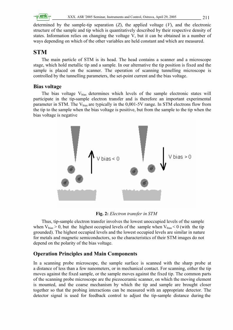
Bias voltage The bias voltage Vbias determines which levels of the sample electronic states will
participate in the tip-sample electron transfer and is therefore an important experimental parameter in STM. The Vbias are typically in the 0,001-5V range. In STM electrons flow from the tip to the sample when the bias voltage is positive, but from the sample to the tip when the bias voltage is negative
Fig. 2: Electron transfer in STM
Thus, tip-sample electron transfer involves the lowest unoccupied levels of the sample when Vbias > 0, but the highest occupied levels of the sample when Vbias < 0 (with the tip grounded). The highest occupied levels and the lowest occupied levels are similar in nature for metals and magnetic semiconductors, so the characteristics of their STM images do not depend on the polarity of the bias voltage.
Operation Principles and Main Components
In a scanning probe microscope, the sample surface is scanned with the sharp probe at a distance of less than a few nanometers, or in mechanical contact. For scanning, either the tip moves against the fixed sample, or the sample moves against the fixed tip. The common parts of the scanning probe microscope are the piezoceramic scanner, on which the moving element is mounted, and the coarse mechanism by which the tip and sample are brought closer together so that the probing interactions can be measured with an appropriate detector. The detector signal is used for feedback control to adjust the tip-sample distance during the

XXX. ASR '2005 Seminar, Instruments and Control, Ostrava, April 29, 2005 212
scanning. The main components of scanning tunneling microscopes are shown on fig. 2.
Fig. 3: Scheme of the STM
The microscope head contains the scanner, the coarse mechanism, the probing tip, and the detector. Instrument operations are performed through the electronic unit controlled by the computer station. The software allows one monitor the tip-sample approach, record the strength of the probing interaction as a function of the tip position, convert the collected information into the image on the screen, and store the data in the computer.
Tip-Sample Approach an Electronic Feedback
The strength of the local probing interactions between the tip and the sample (i.e., the tunneling current in STM and the repulsive force in contact mode AFM) becomes measurable only when tip is positioned close enough to the sample surface (Tománek 2000). To prevent any possible damage of the sample by a tip-sample contact, the approach of the tip to the sample should be delicate. Initially the tip and sample are put close to each other by manually rotating the high-precision mechanical screws which are incorporated into the microscope stage. This procedure is facilitated by an optical control, when a scanning probe microscope is combined with an optical microscope or optical camera system. Closer approach is performed by the stepper motor, which brings the tip to the sample at separations that can be controlled by the scanner. The final adjustment of the tip-sample separation, to the value at which the probing interaction reaches the set-point level determined by the user, is performed by the scanner.
After this engagement, the lateral scanning is activated. The scanning tip can crash into the sample surface because of surface roughness and imperfect tip-sample alignment, unless the scanning is performed with a feedback mechanism. The difference ∆ between the actual and the set-point values of the probing interaction is used for the feedback control. The

XXX. ASR '2005 Seminar, Instruments and Control, Ostrava, April 29, 2005 213
electronic feedback system generates the response to the scanner, to adjust the vertical position to eliminate the difference ∆. Different types of feedback function (e.g., linear and logarithmic) can be used, depending upon the known or presumed relationship between the probing interaction and the tip-sample separation. The accuracy of imaging is strongly influenced by the feedback gain parameters. Use of very low gains keeps the tip position constant, whereas use of very high gains renders unstable the electronic circuit controlling the feedback, because the piezodrive and the current amplifier cannot respond instantaneously. Therefore the scanning should be performed with moderate gain parameters, which are commonly adjusted by the user.
TS 3130 Example of the STM microscopes is instrument made by TESCAN Company. Its name
is TS 3130. This instrument is without vacuum chest and operates with air barrier. In this instrument the tip position is fixed and the sample is placed on the scanner (Tománek, 2002).
Fig. 4: STM probe-sample system
TS 3130 can operate in two modes, constant current mode and constant height mode.
Constant height mode
The value of the tunnel current, which is thorough the air barrier is very depend on the distance between the probe and the sample. If a probe of the microscope is kept in constant height Z above the object, which is not ideally smooth, the electric current is changing in dependence on thin of the air barrier. If the size of the passing current is known, the relief of the sample can be reconstructed. Figure 2 shows a model of the probe-sample system during scanning the metal material.
Constant current mode
In this mode, the current is scanned, modified and fetched to the input of the

XXX. ASR '2005 Seminar, Instruments and Control, Ostrava, April 29, 2005 214
nanomanipulator, whereby is kept constant distance between probe of the STM and tested sample. To construct the image is necessary to scan movement of the manipulator.
Nanomanipulator In this case the instrument made by Physik Instrumente is used. Manipulator is controlled
by control unit PZT. In the input of PZT a signal in range from -2V to + 10V of DCV can be fetched. Usually, we test this instrument in three different frequencies, e.g. for STM the frequencies until 50 Hz are used. But, how one can see from the following, the manipulator is much better than this “limit”.
The signal with various frequencies is fetched to the input of the oscilloscope and to the PZT-servo controller E-5509.C3A, too. The reaction of the capacitive sensors of mouvement of the sample is displayed as output from PZT.
Fig. 5: In/Out from PZT-servo controller , E-5509.C3A by 10 Hz
Fig. 6: In/Out from PZT-servo controller , E-5509.C3A by 100 Hz
Fig. 7: In/Out from PZT-servo controller , E-5509.C3A by 200 Hz
In Out
In Out
Out In

XXX. ASR '2005 Seminar, Instruments and Control, Ostrava, April 29, 2005 215
Conclusion In present, there is a running project in our department, which object is to join STM and SNOM (Scanning Near-field Optical Microscopy) method (Tománek, 2002). Despite of similarity of these two methods, the connection of both will be quite difficult, but not impossible. It is necessary to know very well possibilities of SNOM and STM probes and problems of their movements to complete this task.
Main problems of probe movement were described (Kala, 2004) and some realisations from STM and SNOM topics were also published (e.g., Tománek, 2000). In the first stage of the work, we focused our effort on the theory of the electron and photon tunnel effects. This information is necessary to understand STM and SNOM principle. In the last part of the paper we were inquired into nanomanipulator made by Physik Instrumente. We measured its response to the input signal. The experimental results show that the instrument is efficient up to 200 Hz, what is more better than we can use by scanning process in STM or SNOM methods.
Acknowledgement This paper is based on the research supported by the Research project MSM 0021630503.
References BONNELL, D.A 1993.: Scanning Tunneling Microscopy and Spectroscopy, VCH Publishers,
New York, 1993, ISBN 0-89573-768-X. KALA, J.: Scanning Tunnelling Microscopy 2004, Workshop NDT 2004, Brno University of
Technology, p. 75-79, ISBN 80-7204-371-4. MAGONOV, S.N., WHANGBO. M. 1996. Surface Analysis with STM and AFM Weinheim.
ISBN 3-527-29313-2. TOMÁNEK, P. 2000 Nanotechnologie a optická nanometrologie, VUT Brno, ISBN 80-214-
1589-4. TOMÁNEK,P. 2002 Optická tunelová mikroskopie s lokální sondou, In FRANK, L., KRÁL,
J., (Eds) Metody analýzy povrchu: iontové, sondové a speciální metody, Academia Praha, ISBN 80-200-0594-3.