CONTROL ASPECTS OF A DOUBLE-INPUT BUCKBOOST …power.mst.edu › media › academic › power ›...
81
Transcript of CONTROL ASPECTS OF A DOUBLE-INPUT BUCKBOOST …power.mst.edu › media › academic › power ›...


CONTROL ASPECTS OF A DOUBLE-INPUT BUCKBOOST
POWER ELECTRONIC CONVERTER
by
DEEPAK SOMAYAJULA
A THESIS
Presented to the Faculty of the Graduate School of the
MISSOURI UNIVERSITY OF SCIENCE AND TECHNOLOGY
In Partial Fulfillment of the Requirements for the Degree
MASTER OF SCIENCE IN ELECTRICAL ENGINEERING
2009
Approved by
Mehdi Ferdowsi, Advisor
Norman R. Cox
Jonathan W. Kimball

2009
DEEPAK SOMAYAJULA
ALL RIGHTS RESERVED

iii
ABSTRACT
Systems in which two or more energy sources combine to supply power to a
common load are called hybrid energy systems. Applications of these systems have grown
due to their flexibility and reliability. Hybrid energy systems have been successfully
implemented in hybrid electric vehicles and wind-solar systems where two or more energy
sources share the same load. Double-input (DI) dc-dc power electronic converters
(DIPECs) have been gaining popularity in hybrid energy systems due to their reduced
component count and control simplicity. In addition, employing DIPECs increases the
reliability, stability, and flexibility of the system. In this thesis, a small-signal model for
one of the DIPEC topologies, the DI buckboost converter, is developed and compensator
design is carried out based on the small-signal model. The compensators are designed to
accommodate optimal power sharing between the sources. Theoretically, it is also proven
in this thesis that the two inputs of the DI buckboost topology can be independently
controlled which gives great flexibility in terms of the compensator design. Time domain
analysis of the system is carried out with the compensators included and the results agree
with the theoretical analysis. In addition to the small-signal modeling, a new control
method called offset time control is also introduced and successfully applied to a DIPEC
topology in this thesis. The control scheme is based on adjusting the offset time between
the switching commands; which is proven to have a direct impact on the amount of
current drawn from each input. Small-signal modeling of the offset time control scheme
has been carried out to prove the improvement in the speed of response of the system
when the offset time control scheme is applied.

iv
ACKNOWLEDGEMENTS
I would like to thank my advisor, Dr. Mehdi Ferdowsi, for giving me the
opportunity to work on the project, and for constantly motivating me in my research. I
would also like to thank Dr. Norman Cox and Dr. Jonathan Kimball for serving on my
committee. All three of them have been a great source of inspiration to me.
I would like to thank my lab mates Andrew Meintz, Seyed Mostafa Khazraei, and
Anand Prabhala for giving me valuable inputs on the topic. I would also like to thank my
roommates and friends for being a constant source of support while away from family.
I‟m also grateful to our Department Secretary, Mrs. Regina Kohout for guiding me
through the paperwork and other departmental procedures.
I would like to especially thank my father, S. N. Rama Rao and my mother, S.
Lakshmi for emphasizing the importance of good education all through my life. I would
also like to thank my sister and a few of my friends for encouraging me to pursue graduate
studies in the US. Lastly, I would like to thank everybody else who influenced my life in a
positive way.

v
TABLE OF CONTENTS
Page
ABSTRACT ................................................................................................................... iii
ACKNOWLEDGEMENTS ............................................................................................ iv
LIST OF ILLUSTRATIONS ......................................................................................... vii
LIST OF TABLES ......................................................................................................... ix
SECTION
1. INTRODUCTION ...................................................................................................1
1.1. THE IMPORTANCE OF MULTI-INPUT CONVERTERS .............................1
1.2. ADVANTAGES AND CHALLENGES OF MULTI-INPUT
CONVERTERS ...............................................................................................2
1.2.1. Flexibility of the DIPEC Topologies in Power Sharing ............................3
1.2.2. Control Challenges .................................................................................8
1.3. SMALL-SIGNAL MODELING .......................................................................9
1.4. OFFSET TIME CONTROL ........................................................................... 10
1.5. THESIS ORGANIZATION ........................................................................... 10
2. SMALL-SIGNAL ANALYSIS OF A DI BUCKBOOST CONVERTER ............... 12
2.1. DI BUCKBOOST CONVERTER .................................................................. 12
2.2. DEVELOPMENT OF THE SMALL-SIGNAL MODEL ................................ 14
2.3. TRANSFER FUNCTIONS DERIVATION BASED ON THE SMALL-
SIGNAL MODEL ......................................................................................... 18
2.4. VERIFICATION OF THE TRANSFER FUNCTIONS BASED ON TIME
DOMAIN ANALYSIS................................................................................... 23
3. COMPENSATOR DESIGN AND INDEPENDENT CONTROL OF THE
LOOPS ................................................................................................................. 31
3.1. INDEPENDENT CONTROL OF THE LOOPS ............................................. 32
3.2. CURRENT COMPENSATOR GC2(S) DESIGN ............................................ 35
3.3. VOLTAGE COMPENSATOR GC1(S) DESIGN ............................................ 39
3.4. TIME-DOMAIN SIMULATION OF THE CLOSED LOOP SYSTEM ......... 41
4. OFFSET TIME CONTROL IN A DI BUCKBOOST CONVERTER .................... 45

vi
4.1. OFFSET TIME CONTROL SCHEME .......................................................... 46
4.2. CONTROL SCHEME REALIZATION ......................................................... 49
4.3. SIMULATION RESULTS FOR OPEN-LOOP RESPONSE .......................... 52
4.4. SMALL-SIGNAL ANALYSIS WITH OFFSET TIME CONTROL ............... 55
4.5. TRANSFER FUNCTION DERIVATION WITH OFFSET TIME
CONTROL INCLUDED ............................................................................... 58
4.6. SIMULATION RESULTS FOR CLOSED-LOOP RESPONSE ..................... 62
4.7. CONCLUSION .............................................................................................. 65
5. CONCLUSION ..................................................................................................... 66
BIBLIOGRAPHY ......................................................................................................... 67
VITA ............................................................................................................................. 71

vii
LIST OF ILLUSTRATIONS
Figure Page
1.1. General block diagram of a system with two single-input dc-dc converters ................4
1.2. Two independent single-input buckboost converters regulating the output voltage
to 90 V .....................................................................................................................4
1.3. General block diagram of a DIPEC topology .............................................................6
1.4. DI buckboost converter regulating the output voltage at 90 V ...................................6
1.5. Flexibility in power sharing of a DI buckboost converter when output voltage and
load are constant .......................................................................................................7
2.1. Block diagram of a DI buckboost converter ............................................................ 13
2.2. Inductor voltage waveform and averaged inductor voltage waveform ...................... 15
2.3. Capacitor current waveform and averaged capacitor current waveform ................... 15
2.4. Small-signal model of a DI buckboost converter ...................................................... 18
2.5. Small-signal model of a DI buckboost converter when 0ˆˆˆ212 vvd ......................... 19
2.6. Proposed control procedure with independent control of the loops to realize the
control objective ..................................................................................................... 24
2.7. Block diagram showing the effect of small-signal variations in )(ˆ1 td on )(ˆ tvo .......... 26
2.8. Simulation setup for measuring the effect of small-signal variations in )(ˆ1 td on
)(ˆ tvo ...................................................................................................................... 27
2.9. Bode plot for the transfer function Gvd1(s) ............................................................... 27
2.10. Block diagram showing the effect of small-signal variations in )(ˆ2 td on )(ˆ
2 tis ....... 29
2.11. Bode plot for the transfer function Gis2d2(s)............................................................ 29
3.1. Block diagram of the control system for case 2 where Is2 and V0 are constant .......... 32
3.2. Block diagram of the converter system with the inner current loop closed ............... 33
3.3. Bode plots of the functions Gis2d2(s), Gc2(s) and Ti(s) of the system .......................... 36
3.4. Comparison between Gvd1(s) and Gnew(s) to verify the independency of the loops ..... 38
3.5. Small-signal control loop of the DI buckboost converter where Is2 and V0 are
constant and the loops are independently controlled ................................................ 39
3.6. Bode plots of the functions Gvd1(s), Gc1(s) and Tv(s) of the system ........................... 41

viii
3.7. Output voltage waveform for a step change in load from 10 to 5Ω at t=0.015s
with the current and voltage loop closed with compensators Gc1(s) and Gc2(s) ......... 42
3.8. Average current IS1 waveforms for a step change in load from 10 to 5Ω at
t=0.015s with both loops closed .............................................................................. 43
3.9. Average current Is2 waveforms for a step change in load from 10 to 5Ω at
t=0.015s with both loops closed .............................................................................. 43
4.1. Inductor current waveform in the steady state operation .......................................... 45
4.2. Typical plot of α vs. D12 .......................................................................................... 48
4.3. Block diagram of the overall system ........................................................................ 50
4.4. Block diagram of the power sharing controller ........................................................ 51
4.5. Pulse width modulation block and delay D12 between S1 and S2............................... 51
4.6. Variations of α vs. D12 ............................................................................................. 53
4.7. Variations of <is1> and <is2> vs. D12 ........................................................................ 53
4.8. Step response of α for a step change in D12 from 0.1 to 0.35 ................................... 54
4.9 Small-signal model of a DI buckboost converter with offset time control .................. 58
4.10 Block diagram of the converter system with the inner offset time control loop
closed ..................................................................................................................... 59
4.11 Bode plots of the functions Gis1d1(s), Gis1d1_offfset(s) and Tα(s) of the system .............. 61
4.12. Output voltage V0 waveforms with and without D12 control for a step change
in Iref2 from 9 to 7 A .............................................................................................. 64
4.13. Average current of source 1 <is1> waveforms with and without D12 control
for a step change in Iref2 from 9 to 7 A ................................................................... 64
4.14. Average current of source 2 <is2> waveforms with and without D12 control
for a step change in Iref2 from 9 to 7 A ................................................................... 65

ix
LIST OF TABLES
Table Page
2.1. Modes of operation of a DI buckboost converter ..................................................... 13
3.1. Different control strategies for DI converters .......................................................... 31

1. INTRODUCTION
1.1. THE IMPORTANCE OF MULTI-INPUT CONVERTERS
Wind and solar energy generation is on the rise along with other green energy
sources. The intermittent nature of these energy sources is the main drawback which has
prevented their complete integration into mainstream energy generation. To address this
issue, combining various energy sources with each other to form a hybrid energy system is
proposed in the literature [1]. Batteries, ultra-capacitors, and flywheels are the most
common energy storage mechanisms used to hybridize energy systems. Hybrid electric
power-trains are other examples for energy systems with multiple sources. Hybridization
can also happen at the energy storage level to combine ultra-capacitor and batteries
together in order to make high power and high energy density storage systems.
In general, a dc-dc converter is required to integrate each energy related
component into the system. Integrating each energy source with a dc-dc converter is
expensive, bulky, less efficient, and hard to control. To overcome these shortfalls, using a
single dc-dc isolated or non-isolated multi-input converter is proposed [1-16]. Utilizing a
single dc-dc multi-input converter to integrate all the energy sources provides several
advantages [7], including reduced component count, potential reduction in weight, control
simplicity, and flexibility in the integration of the sources. Multi-input converters are
much like their single-input counterparts in terms of the types of the components being
used and the way they are connected. However, they are generally powered by at least
two energy sources. In this thesis, the analysis and the discussion are based on DI dc-dc
power converters (DIPECs), however, the same can be extended to other systems with
more than two inputs.

2
1.2. ADVANTAGES AND CHALLENGES OF MULTI-INPUT CONVERTERS
Among several advantages [7], reduced component count, flexibility and control
simplicity make DIPECs as attractive options to be utilized in hybrid energy systems
where the input supplied power and the output load demand are variable. Several isolated
and non-isolated DIPECs have been introduced, analyzed, and compared in the literature
[9-16] including DI buck, buckboost, and buck-buckboost converters [9]. As suggested
in [17] various topologies of these converters can be explored just by varying the number
of common components. The authors of [17] also explore and compare various other
topologies based on their reliability, flexibility, modularity potential, and cost.
DIPECs are also proven to be more flexible because various combinations of input
voltages can be used to provide various combinations of output voltages. Compared to
two single-input dc-dc converters which integrate two inputs to supply a common load,
using a DIPEC is considered more advantageous in this case. This is because the inputs in
a DIPEC topology would collaborate together to provide the required output voltage;
whereas regulating the dc-bus voltage in the case with two single input converters would
be much harder since the individual inputs compete to meet the load demand. The
flexibility aspect of the DIPEC topologies when compared to two single-input dc-dc
converters is explored in the next section.
The main challenge in the DIPEC topologies is the choice of the topology and the
choice and implementation of the control strategy. Due to the availability of large number
of these topologies the exact choice of the topology for a given application should be
based on the type of the application and cost [17]. Also, the control strategy which
decides on the amount of power supplied by each source plays an important role in DIPEC

3
topologies. And this control strategy varies from application to application thereby
changing the control procedure.
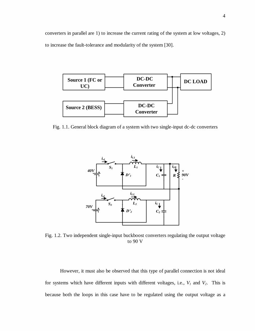
1.2.1. Flexibility of the DIPEC Topologies in Power Sharing. In this section, a
brief comparative study between two systems is carried out to show the amount of
flexibility that is available in DIPEC topologies in terms of power sharing. In the first
system, the sources are integrated to the load through two separate dc-dc converters (see
Figs. 1.1 and 1.2). In the second system, the sources are integrated through a DIPEC
topology (see Figs. 1.3 and 1.4). In both the cases, two different sources of V1=40 V and
V2=70 V are being used to regulate the output voltage of the converter (V0) at 90 V. In
Fig. 1.1, a general block diagram of the first system is presented. In this case, source 1 is
a fuel cell (FC) or an ultra-capacitor (UC) and source 2 can be a battery energy storage
system (BESS). In Fig. 1.2, a specific case of Fig. 1.1 is presented where two single-input
dc-dc buckboost converters are connected in parallel at the output to provide a constant
output voltage of 90 V. It can be clearly seen from Fig. 1.2 that two capacitors and two
inductors are needed in this case which adds to the cost, weight, and losses of the system.
The output voltage equation for the system (see Fig. 1.2) is given by [28, 29]:
)1()1( 2
220
1
110
D
VDVand
D
VDV
(1.1)
where D1 and D2 and are the duty ratios of switches S1 and S2, respectively. Therefore, in
order to regulate the output voltage at 90 V there is only one solution for (1.1) which is
given by D1=0.69 and D2=0.5625. The main advantages of connecting two dc-dc
4
converters in parallel are 1) to increase the current rating of the system at low voltages, 2)
to increase the fault-tolerance and modularity of the system [30].
Source 1 (FC or
UC)
DC-DC
Converter
Source 2 (BESS)
DC LOAD
DC-DC
Converter
Fig. 1.1. General block diagram of a system with two single-input dc-dc converters
70VD’2
40VD’1
L1
C1 R
S2
S1
is1
is2
iL1
iC iO
90V-
+
L2
iL2
iC
C2
Fig. 1.2. Two independent single-input buckboost converters regulating the output voltage
to 90 V
However, it must also be observed that this type of parallel connection is not ideal
for systems which have different inputs with different voltages, i.e., V1 and V2. This is
because both the loops in this case have to be regulated using the output voltage as a

5
reference signal and in the absence of any current sharing compensator the two converters
interact with each other which causes oscillations in the output voltage and the duty ratio
of the converter with the lower voltage loop gain gets saturated as mentioned in [30].
Therefore, the converters in this case compete with each other to meet the load demand.
The voltage loop gain of the converters is dependent on the converter parameters
like V1, L1, C1 and V2, L2, C2 and therefore, it is hard to exactly match the voltage loop
gains of converters with non-identical parameters. Therefore, a current sharing
compensator must be used in this case which provides control over the amount of power
supplied by each source. The design of the current sharing compensator is hard and has
only been carried out for systems with equal input voltages and for equal current sharing
among the sources [30-32]. In other words, it is hard to control the amount of power
supplied by the FC or UC and the BESS and the system is not exactly suited for energy or
power diversification between the two sources which is a major drawback of this system.
In the second system, a DIPEC topology is used to integrate both the sources to
the load as shown in Fig. 1.3. In Fig. 1.4, a specific case of a DIPEC topology (DI
buckboost converter) is used to integrate the sources to the load which has a single
inductor and capacitor thereby reducing the number of components in the system. The
steady-state output voltage V0 of the DI buckboost converter can be described as [9, 14]:
)1()1( 21
22
21
110
DD
VD
DD
VDV
(1.2)
where D1 and D2 are again duty ratios of switches S1 and S2, respectively.

6
Source 1 (FC or
UC) Multi-Input or
Double-Input
DC-DC
ConverterSource 2 (BESS)
DC LOAD
Fig. 1.3. General block diagram of a DIPEC topology
70VD2
40VD1
L
C R
S2
S1
is1
is2
iL
iC iO
90V-
+
Fig. 1.4. DI buckboost converter regulating the output voltage at 90 V
In this case, (1.2) has more than one solution and a few of the solutions of (1.2)
along with the average input powers supplied (P1 and P2) are presented in Fig. 1.5. It can
be clearly observed from Fig. 1.5 that while keeping the output voltage and load constant,
the amount of power supplied by each source P1 and P2 can be varied by varying duty
ratios D1 and D2 without changing the inductor size, i.e., without interfering with the
power stage. Thus, it can be concluded that the DI buckboost converter provides a lot of
flexibility in terms of power sharing between the two sources. This flexibility in terms of
power sharing is the main advantage DIPEC topologies provide in renewable energy

7
applications where the sources can be intermittent. However, the flexibility in power
sharing also calls for a well-defined control strategy or control objective which decides on
the amount of power supplied from each source based on factors like battery state-of-
charge (SOC), solar irradiance, etc. Apart from power sharing, the control strategy
should also focus on load regulation through a constant output voltage. These control
challenges are presented in the next section.
1 2 30
100
200
300
400
500
600
700
800
900
1000
P0 (
W)
V1=40V, V
2=70V, P
0=810W
P2=630W
P1=308.5W
P1=453.6W
P1=180W
P2=501.5W
P2=356.4W
D1=0.2, D
2=0.4, V
0=90V D
1=0.323, D
2=0.3, V
0=90V D
1=0.446, D
2=0.2, V
0=90V
Fig. 1.5. Flexibility in power sharing of a DI buckboost converter when output voltage and
load are constant

8
1.2.2. Control Challenges. As mentioned earlier, the control strategy plays a very
prominent role in DIPEC topologies. Most of the work reported in this field only covers
topology exploration and steady state operation of such converters. Different approaches
to synthesize DI converters have also been reported earlier [13-19]. The control aspects
for specific multi-input topologies are discussed in few papers [20-26]. Control of the
amount of power drawn from each of the sources in a hybrid energy system is important.
When the power supplied by one of the sources decreases, the power supplied by other
sources must be managed effectively to meet the load demand.
Power sharing is necessary in hybrid energy systems such as a wind and solar
combination or a battery and ultra-capacitor combination. For instance, on a cloudy day
when the amount of solar power being supplied is less, the amount of power from other
energy sources needs to increase. Also, in a battery and ultra-capacitor combination when
the ultra-capacitor is discharged, the power drawn from the battery should be increased to
meet the load demand. Thus, the controller must be able to control the amount of power
flowing out from each individual source.
In [9], the importance of battery and ultra-capacitor combination for hybrid
electric vehicles is emphasized and the various DIPEC topologies that can be used to
realize the battery and ultra-capacitor integration are explored. One of the DIPEC
topologies explored in [9] is the DI buckboost (see Fig. 1.4) topology which is introduced
in [16]. In [16], a multiple-input buckboost converter is introduced and its steady state
operation is discussed; the analysis and the equations can be simplified to a DI buckboost
converter by assuming only two inputs. The DI buckboost converter is used for
photovoltaic (PV)-grid integration in [21] and it is proven that input powers of the system
9
can be flexibly controlled while maintaining a constant output voltage. In [22], the same
system is controlled such that maximum power is supplied by the PV array using ripple
correlation control and the additional load demand is met by the grid for a constant load.
In [27], the multi-input buckboost topology is slightly modified for bidirectional power
flow and for operating the converter in all the three modes i.e. buck, boost and buckboost
modes.
In this thesis, the same DI buckboost converter is controlled; however, the control
objective in this case is different and the controller design is based on small-signal
modeling of the DIPEC topologies which has not been reported earlier. In this thesis, the
control objective is power sharing between the sources (e. g. battery and ultra-capacitor)
for a variable load, where one of the sources is expected to supply a constant power and
the other source is expected to meet the excess load demand during load variations while
the output voltage is regulated. The authors of [23] propose a similar control objective
for another DIPEC topology, the DI buck-buckboost converter.
1.3. SMALL-SIGNAL MODELING
DIPEC topologies are nonlinear systems just like their single-input counterparts
and they have to be linearized. Linear time invariant (LTI) models of the converters are
necessary for a systematic controller design. Development of such models is also crucial
for analyzing system stability and for designing optimal compensators. In this thesis, the
LTI small-signal model of the DI buckboost converter is developed. Various transfer
functions necessary for realizing the control objective mentioned in the previous section
are also developed. In this thesis, it is analytically proven in that the two control loops

10
controlling the two switches S1 and S2 are nearly independent of each other for the DI
buckboost converter. This feature of the loops being independently controllable makes the
compensator design much simpler as the two compensators can now be independently
designed. Compensator design based on the transfer functions is carried out.
1.4. OFFSET TIME CONTROL
In this thesis, it is proven that the offset time between the switch commands has a
direct impact on the power sharing of the two sources. Therefore, the proposed control
method is called offset time control. Apart from the two control variables which happen
to be the switch commands, controlling the offset time as an additional control variable
gives an extra degree of freedom in meeting the control objectives. It is also shown that
using the offset time as an additional control variable helps in regulating the output voltage
faster when compared to a system with no offset time control.
1.5. THESIS ORGANIZATION
This thesis is organized into five sections; in Section 2 the small-signal modeling of
the DI buckboost converter is carried out. Compensator design based on models
developed in Section 2 is carried out in Section 3. It is also analytically proven in this
section that the two control loops which control the two control inputs are nearly
independent of each other and the compensators for the loops can be independently

11
designed. Offset time control scheme and its relevant equations are developed in Section
4 in which the advantages of having offset time control are discussed. Conclusions and
future work are presented in Section 5.

12
2. SMALL-SIGNAL ANALYSIS OF A DI BUCKBOOST CONVERTER
Power electronic converters are nonlinear systems and to test the transient stability
they have to be linearized by carrying out small-signal analysis. Compensators can then be
designed based on the developed Linear Time Invariant (LTI) models in order to meet
various control objectives. Small-signal analysis for single input dc-dc converters is very
well established in the literature [28, 29]. However, small-signal modeling for DIPEC
topologies has not been reported yet. Although, the control of DIPEC topologies has
been reported in the literature [21, 23], a systematic design procedure of compensators
based on LTI models has not been reported yet.
Small-signal models for the DIPEC topologies are necessary in order to optimize
the compensator design and to provide a stable system which meets all the control
objectives. This being the intention, the small-signal analysis of a DI buckboost converter
is carried out in this section. A small-signal circuit model for the topology is also
developed and various transfer functions that are responsible for the control of the
converter are derived and analyzed. Similar analysis can be carried for other DIPEC
topologies which are listed in [17] and the required transfer functions can then be derived
from the obtained small-signal models.
2.1. DI BUCKBOOST CONVERTER
The circuit diagram of a DI buckboost converter is shown again in Fig. 2.1 [9, 12,
16, and 21]. In this topology, switch S1 can be any kind of switch as long as V1 is greater
than V2. However, if V1 is not guaranteed to be greater than V2 then S1 needs to be a
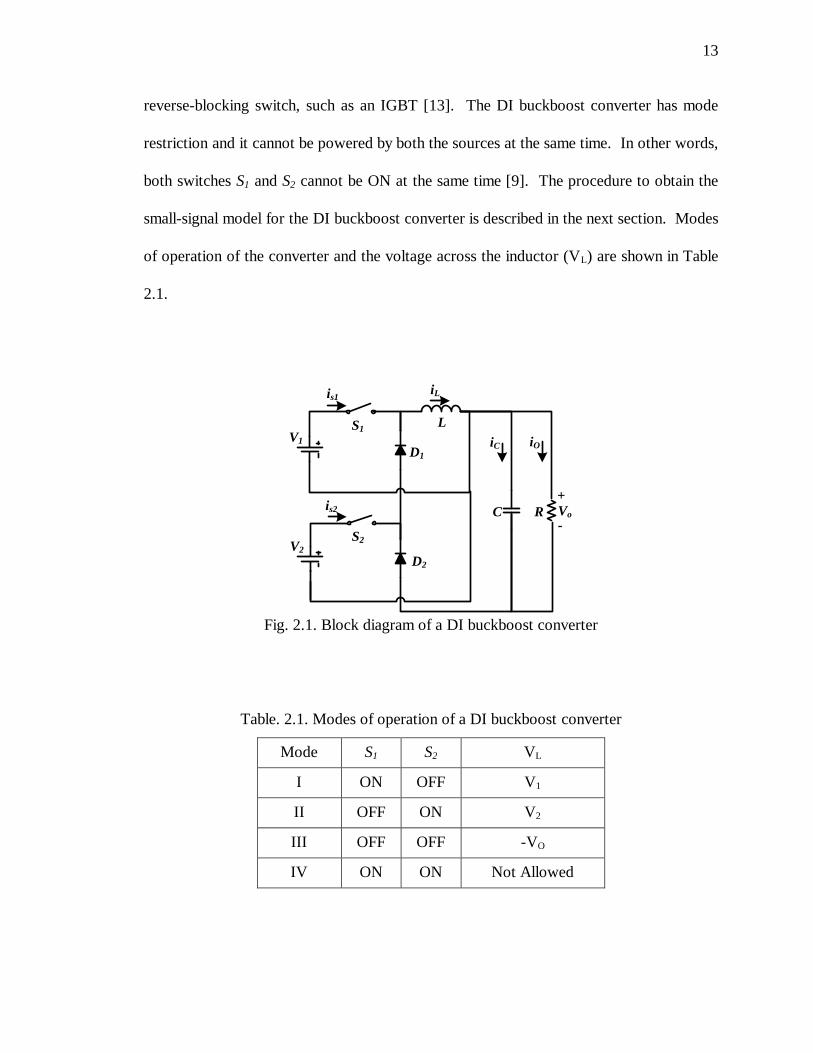
13
reverse-blocking switch, such as an IGBT [13]. The DI buckboost converter has mode
restriction and it cannot be powered by both the sources at the same time. In other words,
both switches S1 and S2 cannot be ON at the same time [9]. The procedure to obtain the
small-signal model for the DI buckboost converter is described in the next section. Modes
of operation of the converter and the voltage across the inductor (VL) are shown in Table
2.1.
V2
D2
V1
D1
L
C R
S2
S1
is1
is2
iL
iC iO
Vo
-
+
Fig. 2.1. Block diagram of a DI buckboost converter
Table. 2.1. Modes of operation of a DI buckboost converter
Mode S1 S2 VL
I ON OFF V1
II OFF ON V2
III OFF OFF -VO
IV ON ON Not Allowed

14
2.2. DEVELOPMENT OF THE SMALL-SIGNAL MODEL
In a DI buckboost converter, the time varying circuit averaged equations (see
Figs.2.2 and 2.3) which describe the low frequency behavior of the system are:
S
s
s To
TL
TL tvtdtdtvtdtvtddt
tidLtv )()()(1)()()()(
)()( 212211 (2.1)
S
SS
S TL
ToTo
TC titdtdR
tv
dt
tvdCti )()()(1
)()()( 21 (2.2)
where d1(t) and d2(t) are the time dependent duty ratios of switches S1 and S2,
respectively. Equation (2.1) is obtained by finding the average of the voltage across the
inductor vL(t) during the ON time of the switches which is indicated by the dashed line in
Fig. 2.2. Then average vL(t) during the OFF time is found which is indicated by the other
dashed line. The actual average inductor voltage during the whole switching cycle is
shown in (2.1) is found by averaging the inductor voltage vL(t) during the ON time and
OFF time of the swithches and is indicated by the dotted line in the Fig. 2.2. In steady
state this dotted line is very close to zero assuming there are no inductor current losses.
Similar procedure is used to obtain (2.2) by averaging the capacitor current waveform
shown in Fig. 2.3 when the switches are ON and OFF, respectively. The dotted lines
shown in Figs. 2.2 and 2.3 represent the circuit averaged equations of (2.1) and (2.2) and
the system would follow these dotted lines in a time-domain simulation when the circuit
averaged model is used.
However, (2.1) and (2.2) both have terms which are products of time varying
quantities and therefore the model is still a non-linear model and it cannot be used to

15
STo tv )(
SS ToTL tvtdtdtvtdtvtdtv )())()(1()()()()()( 212211
)()()()( 2211 tvtdtvtd
sTtd )(1 sTtd )(2
sTtdtd ))()(1( 21
)(1 tv)(1 tv
)(2 tv
Lv
sTt
Fig. 2.2. Inductor voltage waveform and averaged inductor voltage waveform (indicated
by dotted line)
R
tvSTo )(
S
S
S TL
To
TC titdtdR
tvti )())()(1(
)()( 21
R
tvti S
S
To
TL
)()(
STtdtd ))()(1( 21 STtd )(2STtd )(1
sT t
Ci
Fig. 2.3. Capacitor current waveform and averaged capacitor current waveform (indicated
by dotted line)

16
predict the system behavior during load or input voltage transients. The model given by
(2.1) and (2.2) can be linearized around a steady state operating point by including small-
signal ac perturbations around the operating point. Then the time varying quantities in
(2.1) and (2.2) change to:
)(ˆ)(
)(ˆ)(
)(ˆ)(
)(ˆ)(
)(ˆ)(
)(ˆ)(
0
222
111
222
111
tiIti
tvVtv
tvVtv
tvVtv
tdDtd
tdDtd
LLTL
oTo
S
S
(2.3)
In (2.3) all the values in capital case are steady state values and all the values with
a hat are small-signal ac perturbations. Replacing the time varying parameters in (2.1) and
(2.2) with the values in (2.3) would give:
))(ˆ))((ˆ)(ˆ1(
))(ˆ))((ˆ())(ˆ))((ˆ())(ˆ(
02211
22221111
tvVtdDtdD
tvVtdDtvVtdDdt
tiIdL
o
LL
(2.4)
))(ˆ))((ˆ)(ˆ1())(ˆ())(ˆ(
221100 tiItdDtdD
R
tvV
dt
tvVdC LL
oo
(2.5)
Neglecting the product of small-signal perturbed ac terms and equating the derivatives of
the steady state terms to zero on both sides in (2.4) and (2.5) yeilds:
)(ˆ)1()(ˆ)()(ˆ)()(ˆ)(ˆ)(ˆ
212021012211 tvDDtdVVtdVVtvDtvDdt
tidL o
L (2.6)
)(ˆ)1())(ˆ)(ˆ()(ˆ)(ˆ
2121 tiDDItdtdR
tv
dt
tvdC LL
oo
(2.7)

17
Converting (2.6) and (2.7) into frequency domain using the Laplace Transformation would
give[28, 29]:
)(ˆ)1(
)(ˆ)()(ˆ)()(ˆ)(ˆ)(ˆ
21
2021012211
svDD
sdVVsdVVsvDsvDsisL
o
L
(2.8)
)(ˆ)1())(ˆ)(ˆ()(ˆ
)(ˆ2121 siDDIsdsd
R
svsvsC LL
oo (2.9)
The process of obtaining small-signal model for the DIPEC topologies is very
similar to the process ascertained for single-input dc-dc converters [28, 29]. The only
difference for DIPEC topologies is that in this case there are two control inputs 21
ˆ,ˆ dd and
also two disturbance inputs 21ˆ,ˆ vv . Multi-phase converters and converters connected in
parallel also have more than one control input as discussed in [31]; however, in such
systems the control inputs are generally made equal (i.e. ddd ˆˆˆ21 ) for equal current
sharing in the inductors. The input side of the small-signal model which has the switch
current perturbations can be obtained by perturbing the steady state switch current
equations. The equations for steady state average switch currents Is1 and Is2 are given by
Ls IDI 11 (2.10)
Ls IDI 22 (2.11)
Equations (2.10) and (2.11) in perturbed form give
)(ˆ)(ˆ)(ˆ
))(ˆ))((ˆ()(ˆ
111
1111
siDsdIsi
siIsdDsiI
LLs
LLss
(2.12)

18
)(ˆ)(ˆ)(ˆ
))(ˆ))((ˆ()(ˆ
222
2222
siDsdIsi
siIsdDsiI
LLs
LLss
.
(2.13)
The small-signal model shown in Fig. 2.4 is obtained by combining (2.8), (2.9),
(2.12) and (2.13) into current sources, voltage sources, current dependent sources, and
voltage dependent sources. In Fig. 2.4, the voltage and current sources which have either
of the control inputs 1d or
2d in the product are independent sources and all the other
sources which have the disturbance inputs 1v or 2v , inductor currentLi , and output voltage
ov states are dependent sources.
sL
-
+
1ˆsi
1v1dIL LiD ˆ
1
2ˆsi
2v2dIL LiD ˆ
2
+-
-+
11vD
22vD
-ovDD ˆ)1( 21 +
22ˆ)( dVV o11
ˆ)( dVV oLi
LiDD ˆ)1( 21 )ˆˆ( 21 ddIL ov
oi
1
sC R
Fig. 2.4. Small-signal model of a DI buckboost converter
2.3. TRANSFER FUNCTIONS DERIVATION BASED ON THE SMALL-SIGNAL
MODEL
It can be observed from Fig. 2.4 that the model has two control inputs 1d , 2d and
two disturbance inputs 21ˆ,ˆ vv and all the other perturbations are dependent on these four
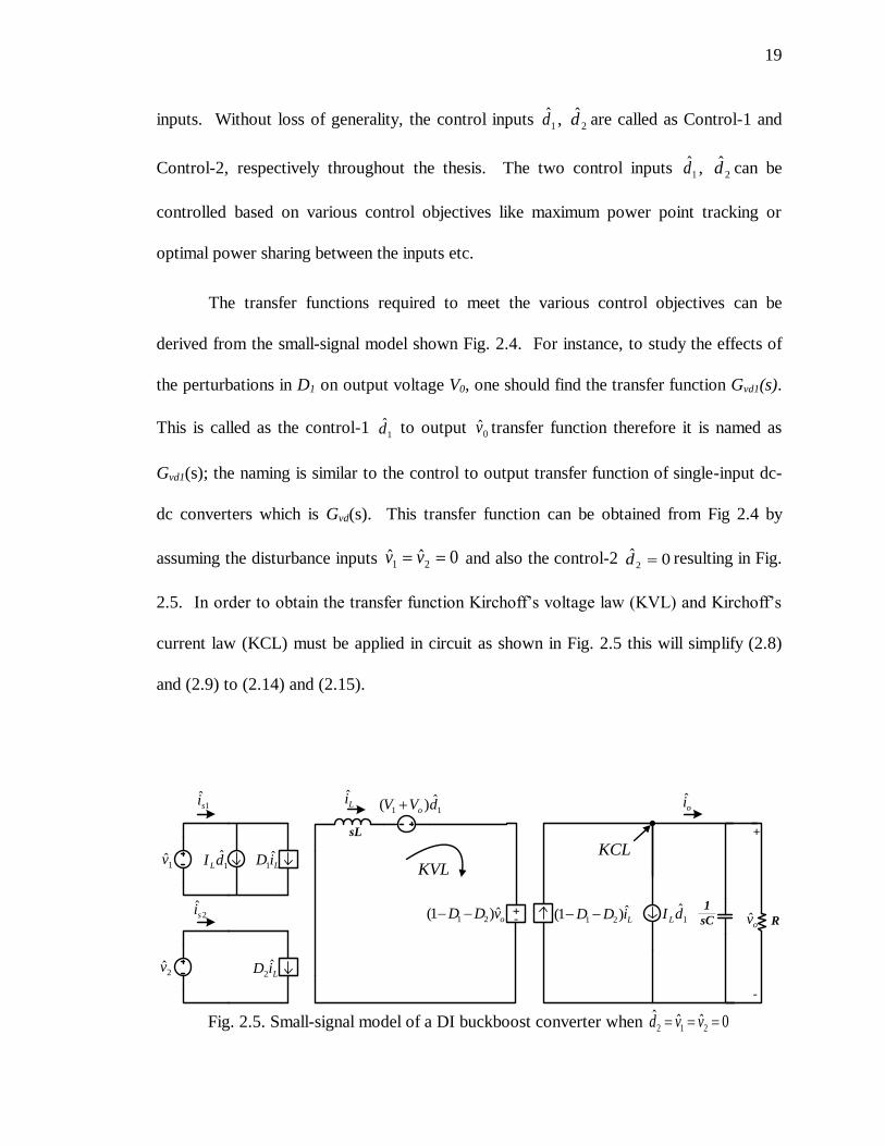
19
inputs. Without loss of generality, the control inputs 1d , 2d are called as Control-1 and
Control-2, respectively throughout the thesis. The two control inputs 1d , 2d can be
controlled based on various control objectives like maximum power point tracking or
optimal power sharing between the inputs etc.
The transfer functions required to meet the various control objectives can be
derived from the small-signal model shown Fig. 2.4. For instance, to study the effects of
the perturbations in D1 on output voltage V0, one should find the transfer function Gvd1(s).
This is called as the control-1 1d to output 0v transfer function therefore it is named as
Gvd1(s); the naming is similar to the control to output transfer function of single-input dc-
dc converters which is Gvd(s). This transfer function can be obtained from Fig 2.4 by
assuming the disturbance inputs 0ˆˆ21 vv and also the control-2 0ˆ
2 d resulting in Fig.
2.5. In order to obtain the transfer function Kirchoff‟s voltage law (KVL) and Kirchoff‟s
current law (KCL) must be applied in circuit as shown in Fig. 2.5 this will simplify (2.8)
and (2.9) to (2.14) and (2.15).
sL
-
+
1ˆsi
1v1dIL LiD ˆ
1
2ˆsi
2vLiD ˆ
2
-ovDD ˆ)1( 21 +
11ˆ)( dVV oLi
LiDD ˆ)1( 21 1dI Lov
oi
1
sC R
KVL
KCL
Fig. 2.5. Small-signal model of a DI buckboost converter when 0ˆˆˆ212 vvd

20
sL
svDDsdVVsi o
L
)(ˆ)1()(ˆ)()(ˆ 21101 (2.14)
)(ˆ)1()(ˆ)(ˆ1
211 siDDIsdsvR
sC LLo
(2.15)
Eliminating )(ˆ siLfrom (2.14) and (2.15) results in
sL
svDDsdVVDDIsdsv
RsC o
Lo
)(ˆ)1()(ˆ)()1()(ˆ)(ˆ
1 21101211
(2.16)
Equation (2.16) can be further simplified to
)(ˆ)))(1(
()(ˆ)1(1
10121
2
21 sdsL
VVDDIsv
sL
DD
RsC Lo
(2.17)
Equation (2.17) can be further simplified to
2
21
2
2101
0ˆˆˆ1
1
)1(
)1)((
)(ˆ
)(ˆ)(
212 DDR
LsLCs
sLIDDVV
sd
svsG L
vvd
ovd
(2.18)
This transfer function is a second order system with a resonant pole pair and a
right-half plane (RHP) zero. The RHP zero is a characteristic of the buckboost converters
and it limits the bandwidth of the system. If D2 is zero, then the transfer function will be
reduced to that of a single input buckboost converter [28]. Similarly, the effect of the
perturbations in D2 on the output voltage Vo can be found by assuming 0ˆˆ21 vv and
also control-1 0ˆ1 d and following the same procedure as

21
2
21
2
2102
0ˆˆˆ2
2
)1(
)1)((
)(ˆ
)(ˆ)(
211 DDR
LsLCs
sLIDDVV
sd
svsG L
vvd
ovd
(2.19)
This transfer function is the control-2 to output transfer function and hence its
name is Gvd2(s). Transfer function Gvd2(s) and its response are very similar to Gvd1(s)
except for term V2 in the numerator. This similarity is due to the fact that both the inputs
of the system are connected to the output in a buckboost configuration. Transfer
functions Gvd1(s) and Gvd2(s) would be different in case of other DIPEC topologies like DI
buck-buckboost where one input is connected to the output in the buck configuration and
the other input is connected to the output in the buckboost configuration. In such a case,
it would be easier to regulate the output voltage by controlling the switch of the input
connected in buck configuration; since, there will be a RHP zero in the control to output
transfer function of input connected in buckboost configuration which will limit the
bandwidth of the system. These are some of the design choices that will be available to
the designer which are non-existent in the single-input topologies.
One can also study how perturbations in D1 effect the inductor current and this is
obtained by eliminating )(ˆ svo from (2.14) and (2.15) which leads to
2
21
2
2101
0ˆˆˆ1
1
)1(
)1()1
)((
)(ˆ
)(ˆ)(
212 DDR
LsLCs
IDDsCR
VV
sd
sisG
L
vvd
Lid
(2.20)

22
The control-1 to inductor current transfer function Gid1(s) is important when implementing
a current-mode control scheme for controlling D1 [32]. Similarly, the effect of
perturbations in D2 on the inductor current is given by
2
21
2
2102
0ˆˆˆ2
2
)1(
)1()1
)((
)(ˆ
)(ˆ)(
211 DDR
LsLCs
IDDsCR
VV
sd
sisG
L
vvd
Lid
(2.21)
If the objective is to maintain one of the average switch currents constant the
following transfer functions shown in (2.24) and (2.25) are important in this context.
Control-to-switch current gain for the buck converter has been derived in [33] in which
average switch current in each cycle is controlled using charge control. Similar analysis
can be carried out for the DI buckboost converter to obtain the control-2 to switch current
2 transfer function Gis2d2(s). From Fig. 2.4 the switch current 2 perturbations )(ˆ2 sis
are
given by (2.22) and it is also known that the inductor current perturbations are functions
of both the control inputs1d and
2d as shown in (2.23)
)(ˆ)(ˆ)(ˆ222 siDsdIsi LLs (2.22)
)(ˆ)()(ˆ)()(ˆ2211 sdsGsdsGsi ididL (2.23)
Substittuting (2.23) in (2.22) and commanding the control-1 1d =0 leads to the required
transfer function

23
2
21
2
2102
2
0ˆˆˆ2
222
22
0ˆ2
222
22211222
)1(
)1()1
)((
)(ˆ
)(ˆ)(
)()(ˆ
)(ˆ)(
)(ˆ)()(ˆ)()(ˆ)(ˆ
211
1
DDR
LsLCs
IDDsCR
VV
DIsd
sisG
sGDIsd
sisG
sdsGDsdsGDsdIsi
L
L
vvd
sdis
idL
d
sdis
ididLs
(2.24)
Similar analysis leads to the control-1 to switch current 1 transfer function Gis1d1(s):
2
21
2
2101
1
0ˆˆˆ1
111
)1(
)1()1
)((
)(ˆ
)(ˆ)(
211 DDR
LsLCs
IDDsCR
VV
DIsd
sisG
L
L
vvd
sdis
(2.25)
From (2.24) and (2.25) it can be seen that the transfer functions Gis1d1(s) and Gis2d2(s) are
important when one of the switch currents needs to be maintained constant and thereby
supplying constant power from one of the sources irrespective of the load demand.
2.4. VERIFICATION OF THE TRANSFER FUNCTIONS BASED ON TIME
DOMAIN ANALYSIS
Few of the developed transfer functions are verified in this section. As mentioned
earlier, the control objective in this thesis is to supply constant power from one of the
sources and meet the additional load demand from the other source even during load and
input variations. The control objective can be realized by regulating output voltage V0
through the control of the control variable D1 and by maintaining the average switch
current Is2 as constant through the control of the other control variable D2 as shown in Fig.

24
2.6. In Fig. 2.6, the two loops are being independently controlled and this feature of the
loops being independently controllable will be analytically proved in Section 3.
Voltage
Compensator
Vref
S2S1
PWM
Current
Compensator
PWM
+-
V0
Iref2+-
Is2
D1 D2
Fig. 2.6. Proposed control procedure with independent control of the loops to realize the
control objective
In order to regulate the output voltage by controlling D1, one needs to analyze
transfer function Gvd1(s) =)(ˆ
)(ˆ
1 sd
svo developed in (2.18). This transfer function is obtained at
the following operating point:
V1=40 V, V2=70 V, V0=90 V, L=50 µH, C=120 µF, R=10 Ω, D1=0.2, and D2=0.4
Initially, a time domain simulation is carried out at the same operating point by
inducing small-signal time domain ac sinusoidal perturbations )(ˆ1 td =0.05*sin(2π*f*t) at a
given frequency „f‟. These ac small-signal perturbations impact output voltage V0 and will

25
cause small-signal perturbations of )(ˆ tvo as shown in the block diagram of Fig. 2.7. The
simulation setup for measuring the effect of small-signal variations )(ˆ1 td on )(ˆ tvo is
shown in Fig. 2.8 and the simulation is carried out in Matlab/Simulink. The model is
designed considering all the diodes and switches are ideal. Also, the new model is
designed to based on the equations of the components rather than using the components
directly as this would reduce the simulation time. Apart from that the model is similar to a
switched model of a converter that can be built in PSPICE or Simpower. This impact can
be converted into frequency domain using
dBtd
tv
sd
svsG oo
vd
)(ˆ
)(ˆlog*20
)(ˆ
)(ˆ)(
11
1 (2.26)
Similarly, perturbations are induced at various other frequencies and a comparison
is carried out between the measured Gvd1(s) and predicted Gvd1(s) as shown in the Fig. 2.9.
The predicted function is obtained by calculating Gvd1(s) at the operating point and it is
plotted in MATHCAD as shown in Fig. 2.9. As mentioned previously the system is a
classic two pole system with a RHP zero which further introduces a phase delay of 90˚ in
addition to the 180˚ caused by the resonant pole pair thereby making the system to settle
at a phase angle of -270˚. It can be seen that there is a good match between the
measurements made in time domain and those predicted through the bode plot. This
indicates that the obtained transfer function Gvd1(s) is accurate. It must be noted here that
in real time applications, the time domain measurements are obtained through a network
analyzer [28] or through a digital modulator when the measured signal is discrete in which
case analog modulation results are not accurate [34]. The transfer function Gvd1(s) can

26
therefore be used for designing a compensator for output voltage regulation through
control of D1. Similar analysis can be performed on transfer function Gvd2(s) and its time
domain and frequency domain response would be very similar to Gvd1(s) as discussed
earlier since both the inputs are connected in buckboost configuration to the output.
Therefore, Gvd2(s) can also be used to regulate output voltage V0 using control variable
D2.
V1
S1is1
is2
Double-Input
Buckboost
Converter
L
o
a
dV2
S2
+
-
)(ˆ11 tdD
.2 constD
)(ˆ0 tvV o
Fig. 2.7. Block diagram showing the effect of small-signal variations in )(ˆ1 td on )(ˆ tvo

27
Fig. 2.8. Simulation setup for measuring the effect of small-signal variations in )(ˆ1 td on
)(ˆ tvo
10 100 1 103
1 104
1 105
1 106
1 107
40
20
0
20
40
60
80
Gvd1_measuredn 0
20 log Gvd1 j ( )
fmeasuredn 0
2
10 100 1 103
1 104
1 105
1 106
1 107
360
270
180
90
0
90
A_Gvd1_measuredn 0
A_Gvd1 ( )
fmeasuredn 0
2
Fig. 2.9. Bode plot for the transfer function Gvd1(s)

28
In order to maintain average switch current Is2 constant by controlling duty ratio
D2, a current compensator must be designed (see Fig. 2.6) for transfer function Gis2d2(s) =
)(ˆ
)(ˆ
2
2
sd
sis developed in (2.24). The transfer function Gis2d2(s) developed in (2.24) is therefore
analyzed here to test its accuracy by comparing it to a time-domain simulation. Initially, a
time domain simulation is carried out to study the effect of time domain ac sinusoidal
perturbations in )(ˆ2 td =0.05*sin (2π*f*t) at a given frequency „f‟. These ac small-signal
perturbations will impact the average switch current Is2 of source 2 and it will have small-
signal variations of )(ˆ2 tis as shown in the block diagram of Fig. 2.10 and the simulation
setup is similar to the one shown in Fig. 2.8 except that now D2 is perturbed with )(ˆ2 td
and )(ˆ2 tis is measured. This impact can be converted into frequency domain using
dBtd
ti
sd
sisG ss
dis
)(ˆ
)(ˆlog*20
)(ˆ
)(ˆ)(
2
2
2
2
22 (2.27)
The same procedure is applied at various other frequncies and the measured
Gis2d2(s) is compared with the predicted Gis2d2(s) as shown in Fig. 2.11. The predicted
function is obtained by calculating Gis2d2(s) at the operating point and it is plotted in
MATHCAD as shown in Fig. 2.11. The transfer function follows a single-pole response
at low frequencies dominated by the transfer function Gid2(s) in (2.24) but at high-
frequencies the response is dominated by the inductor current IL and therefore the phase
angle settles at 0˚ at high-frequencies. The good match between the values indicates that

29
the model obtained for the Gis2d2(s) is also accurate and it can be used to design the
current compensator.
V1
S1
Double-Input
Buckboost
Converter
L
o
a
dV2
S2
+
-
)(ˆ22 tdD
.1 constD
)(ˆ0 tvV o)(ˆ
22 tiI ss
1si
Fig. 2.10. Block diagram showing the effect of small-signal variations in )(ˆ2 td on )(ˆ
2 tis
10 100 1 103
1 104
1 105
1 106
1 107
20
0
20
40
60
80
Gis2d2_measuredn 0
20 log Gis2d2 j ( )
f1n 0
2
Fig. 2.11. Bode plot for the transfer function Gis2d2(s)

30
10 100 1 103
1 104
1 105
1 106
1 107
90
60
30
0
30
60
90
A_Gis2d2_measuredn 0
A_Gis2d2 ( )
f1n 0
2
Fig. 2.11. Bode plot for the transfer function Gis2d2(s) (cont.)
Since developed transfer functions Gvd1(s) and Gis2d2(s) are accurate, it is important
to discuss the procedure for the compensator design based on the control objective and to
analytically prove the independency of the two control loops. These results are discussed
and presented in Section 3. These results would aid in the formation of a stable closed-
loop control system which meets all the control objectives and helps in optimizing the
compensator design.

31
3. COMPENSATOR DESIGN AND INDEPENDENT CONTROL OF THE
LOOPS
Compensator design for the DI buck boost converter is presented in this section.
Chen et al. propose the following control strategies for DI buck-buckboost converter
topology in [23], for various types of applications as shown in Table 3.1.
Table. 3.1. Different control strategies for DI converters
Case Source 1 Source 2 Load
1 P1=constant P2=variable Pout=variable
2 P1=variable P2=constant Pout=variable
3 P1=constant P2=constant Pout=constant
It can be seen from the Table 3.1 that cases 1 and 2 are similar and in both of the
cases one of the sources is supplying constant power and the other source is supplying
variable power to meet the load demand during load variations. In case 3 both of the
sources are controlled to supply constant powers and the load must be capable of taking
the amount of supplied power. In cases 1 and 2, constant power is supplied from one of
the sources by commanding the average switch currents, either Is1 or Is2, as constant
through the control of either D1 or D2 alongwith maintaining output voltage regulation by
having V0 constant through the control of the other control variable D2 or D1. The block
diagram showing the control procedure for case 2 is shown in Fig. 3.1 which has been
32
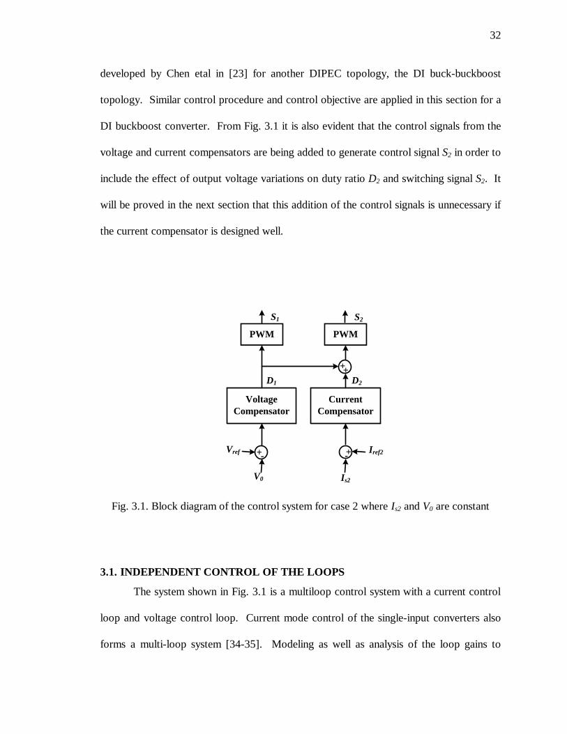
developed by Chen etal in [23] for another DIPEC topology, the DI buck-buckboost
topology. Similar control procedure and control objective are applied in this section for a
DI buckboost converter. From Fig. 3.1 it is also evident that the control signals from the
voltage and current compensators are being added to generate control signal S2 in order to
include the effect of output voltage variations on duty ratio D2 and switching signal S2. It
will be proved in the next section that this addition of the control signals is unnecessary if
the current compensator is designed well.
Voltage
Compensator
Vref
S2S1
PWM
Current
Compensator
PWM
+-
V0
Iref2+-
Is2
++D1 D2
Fig. 3.1. Block diagram of the control system for case 2 where Is2 and V0 are constant
3.1. INDEPENDENT CONTROL OF THE LOOPS
The system shown in Fig. 3.1 is a multiloop control system with a current control
loop and voltage control loop. Current mode control of the single-input converters also
forms a multi-loop system [34-35]. Modeling as well as analysis of the loop gains to

33
predict the stability are complex in the multi-loop systems [35] when compared to single-
loop systems because of interaction between loop gains. Therefore, an effort is made in
this section to simplify the multi-loop system of the DI buckboost converter into several
individual and independent loops. In this section, it is analytically proven that control
inputs )(ˆ1 sd and )(ˆ
2 sd can be independently controlled with each loop having a different
control objective, i.e., one of the loops is able to regulate output voltage V0 and the other
loop is regulating average switch current Is2 of source 2. The inner current control loop is
shown in the Fig. 3.2 and average current mode control (ACMC) scheme is used to keep
switch current Is2 constant. Transfer function Gis2d2(s) (the control-2 to switch current-2
gain) which is responsible for this has been developed and analyzed in Section 2.
However, perturbations in )(ˆ2 sis
are also dependent on the control-1 )(ˆ1 sd and this
dependency is given by transfer function Gis2d1(s) as shown in Fig. 3.2 and in (3.1).
)(22 sG dis
2ˆsi2d
MV
1)(2 sGc
)(12 sG dis
+-
2ˆrefi
++
1d
iT
Fig. 3.2. Block diagram of the converter system with the inner current loop closed
)(ˆ)()(ˆ)()(ˆ2221122 sdsGsdsGsi disdiss (3.1)

34
In order reduce this dependency, the perturbations )(ˆ1 sd are considered as
disturbance signals for the inner current control loop once the loop is closed and this leads
to
)(ˆ)(1
)()(ˆ
)(1
)()(ˆ
21
12
2 sisT
sTsd
sT
sGsi ref
i
i
i
diss
(3.2)
It is also known that the output voltage is a function of both the control input
perturbations and this relation is given as:
)(ˆ)()(ˆ)()(ˆ2211 sdsGsdsGsv vdvdo (3.3)
Replacing )(ˆ2 sd with corresponding perturbations in )(ˆ
2 sis by using Fig. 3.2 results in
)(ˆ)()()(ˆ)()(ˆ
2
2
211 siV
sGsGsdsGsv s
M
cvdvdo (3.4)
Equation (3.4) can be further simplified using (3.2) to
)(ˆ
)(1
)()(ˆ
)(1
)()()()(ˆ)()(ˆ
21122
211 sisT
sTsd
sT
sG
V
sGsGsdsGsv ref
i
i
i
dis
M
cvdvdo
(3.5)
If the current control loop is faster than the voltage loop then 0)(ˆ2 siref and therefore
(3.5) becomes
)(ˆ)(1
)()()()(ˆ)()(ˆ
1
122
211 sdsT
sG
V
sGsGsdsGsv
i
dis
M
c
vdvdo
(3.6)

35
The new transfer function control-1 to output transfer function Gnew(s) shown in (3.7) is
dependent on Gvd2(s), Gis2d1(s) and the current compensator Gc2(s). Gvd2(s) and Gis2d1(s)
functions can be derived following the procedure listed in Section 2 however, the current
compensator Gc2(s) must be designed in order to compare the functions Gvd1(s) and
Gnew(s).
)(1
)()()()(
)(ˆ
)(ˆ)( 122
21
1sT
sG
V
sGsGsG
sd
svsG
i
dis
M
c
vdvd
o
new (3.7)
3.2. CURRENT COMPENSATOR GC2(S) DESIGN
In this section, the current compensator design is discussed for the control of
average switch current. Average current mode control has been extensively reported and
implemented in the literature [31, 32, 36-39] for single-input topologies in which the
average inductor current is generally controlled. Controlling the average inductor current
for equal current sharing between inputs of a parallel connected dc-dc converter is
discussed in [40]. In few papers like [33] and [41], the control of average input switch
current for single-input topologies is proposed. Similar analysis is needed here to maintain
the average switch current of one of the sources in the DI converter constant (in order to
supply constant power from that source). This is the proposed control objective for case
1 and case 2 of Table 3.1.
Here, the analysis would be for case 2 to maintain Is2 constant and for this Gis2d2(s)
is the transfer function for which a current compensator Gc2(s) must be designed in order
to complete the current control loop Ti(s) as shown in Fig. 3.2. Bode plots of the transfer

36
function Gis2d2(s), the compensator Gc2(s) and the loop gain Ti(s) are shown in Fig. 3.3. It
can be observed from Fig. 3.3 that transfer function Gis2d2(s) has enough phase margin.
Therfore, it can be compensated just by using an integrator. However, in doing so the
phase tends to -180˚ in the 1-10 kHz region and so the phase margin would not be enough
in this case. Therefore, a Type-II (proposed in [42-44]) phase lead compensator which
consists of two poles and a zero is used. This compensator gives a phase boost in the 1-
10 kHz region and the gain of the compensator is adjusted to get the desired crossover
frequency of around 2.5 kHz. The compensator Gc2(s) has a zero at frequency fz=1.526
kHz and two poles at frequencies fp1 and fp2 one at origin fp1=0 and the other at fp2=22.07
kHz. The compensator transfer function is
3
3
2
10*07.22*21
10*526.1*21
400)(
s
s
ssGc
(3.8)
10 100 1 103
1 104
1 105
1 106
1 107
40
20
0
20
40
60
80
20 log Gis2d2 j ( )
20 log Gc2 j ( )
20 log Ti j ( )
2
10 100 1 103
1 104
1 105
1 106
1 107
270
180
90
0
90
A_Gis2d2 ( )
A_Gc2 ( )
A_Ti ( )
2 ( )
Fig. 3.3. Bode plots of the functions Gis2d2(s), Gc2(s) and Ti(s) of the system

37
10 100 1 103
1 104
1 105
1 106
1 107
270
180
90
0
90
A_Gis2d2 ( )
A_Gc2 ( )
A_Ti ( )
2 ( )
Fig. 3.3. Bode plots of the functions Gis2d2(s), Gc2(s) and Ti(s) of the system (cont.)
It can be observed from loop gain Ti(s) in Fig. 3.3 that the system has a phase margin of
63˚ at the crossover frequency which is 2.365 kHz. Thus, the inner control Ti(s) is a
stable control loop since its phase margin is positive and the phase margin and cross over
frequency are enough to meet load and line transients with a fast settling time and a low
overshoot. Now that the current compensator Gc2(s) is designed and the inner current
control loop Ti(s) is a stable; the new control-1 to output transfer function Gnew(s) can be
calculated using (3.7). Gnew(s) can be compared to the actual control-1 to output transfer
function Gvd1(s). The bode plots of the transfer functions Gvd1(s) and Gnew(s) are plotted in
Fig. 3.4 and it can be seen that the two functions are close to each other over a wide
frequency range both in terms of the magnitude and phase.

38
10 100 1 103
1 104
1 105
1 106
1 107
40
20
0
20
40
60
80
20 log Gvd1 j ( )
20 log Gnew j ( )
2
10 100 1 103
1 104
1 105
1 106
1 107
270
180
90
0
90
A_Gvd1 ( )
A_Gnew ( )
2 ( )
Fig. 3.4. Comparison between Gvd1(s) and Gnew(s) to verify the independency of the loops
Therefore, it can be concluded that voltage compensator Gc1(s) can be designed
independently neglecting the loop dynamics of current control loop Ti(s). However, it
must be noted that this independent control of the two loops and the negligible effect of
the inner current loop Ti(s) on the outer loop dynamics is true only if current compensator
Gc2(s) is well designed and inner current loop Ti(s) is stable. It has already been proven
that Ti(s) is a stable loop with a positive phase margin and therefore, both Ti(s) and Tv(s)
can be independently controlled as shown in Fig. 3.5.

39
3.3. VOLTAGE COMPENSATOR GC1(S) DESIGN
In this section, voltage compensator which is used to regulate output voltage (V0)
and its design is discussed and inner loop Ti(s) dynamics are neglected as shown in Fig.
3.5. The design procedure is similar to that of voltage mode controller design of single-
input buckboost topology. In [42], the voltage mode controller design for converters with
RHP zeros, i.e., the boost and the buckboost converters operating in CCM and DCM is
elaborately presented. The DI buckboost converter is also operating in CCM and it also
has a RHP zero and therefore, the same design methodology can be extended for this case.
)(1 sGvd
ov1d
MV
1)(1 sGc
refv+-
)(22 sG dis
2ˆsi
MV
1)(2 sGc
+-
2ˆrefi
iT
2d
vT
Fig. 3.5. Small-signal control loop of the DI buckboost converter where Is2 and V0 are
constant and the loops are independently controlled
The voltage compensator must be designed for control-1 to output gain (Gvd1(s))
as shown in Fig. 3.5. Bode plots of transfer function Gvd1(s), voltage compensator Gc1(s),
and loop gain Tv(s) are shown in Fig. 3.6. It can be observed from Fig. 3.6 that the phase

40
angle of Gvd1(s) goes from 0˚ to -180˚ once the system reaches the resonant pole pair
frequency fLC=821.8 Hz and it gradually reaches a phase angle of -270˚ due to the RHP
zero which is present at frequency fRHP=7356 Hz. Therefore, the system requires a phase
boost in the 1-25 kHz region. To provide this phase lead, a Type III compensator with
two zeros and three poles is used. The zeros are placed at frequencies fz1=fz2=575.311 Hz
which is 0.7*fLC based on the design procedure. One of the poles is fixed at the origin
fp1=0 Hz and the other two poles are placed at frequencies fp2=fp3=36.78 kHz which is
above half the switching frequency of 25 kHz. Placing these two poles at higher
frequencies helps in increasing the phase margin of the system and provides good load
regulation. Finally, the gain of the compensator is adjusted to have a crossover frequency
of 1.285 kHz which makes the voltage loop slower than current loop Ti(s). Voltage loop
Tv(s) has to be slower than current loop Ti(s) since in the dc-dc converter the output
voltage states are slower than the inductor current states [29]. The final compensator
transfer function is
2
1
36780*21
311.575*21
30)(
s
s
ssGc
(3.9)
It can be observed from Fig. 3.6 that the system has a phase margin of 42˚ at the required
crossover frequency of 1.285 kHz which makes the voltage loop Tv(s) a stable loop. Now
that compensators Gc1(s) and Gc2(s) are designed, a time domain simulation is carried out
to test the stability of the system during load changes, i.e., for load regulation. And the
41
system has to achieve the control objective as well. These results are presented in the next
section.
10 100 1 103
1 104
1 105
1 106
1 107
80
60
40
20
0
20
40
60
80
20 log Gvd1 j ( )
20 log Gc1 j ( )
20 log Tv j ( )
2
10 100 1 103
1 104
1 105
1 106
1 107
360
270
180
90
0
90
A_Gvd1 ( )
A_Gc1 ( )
A_Tv ( )
2 ( )
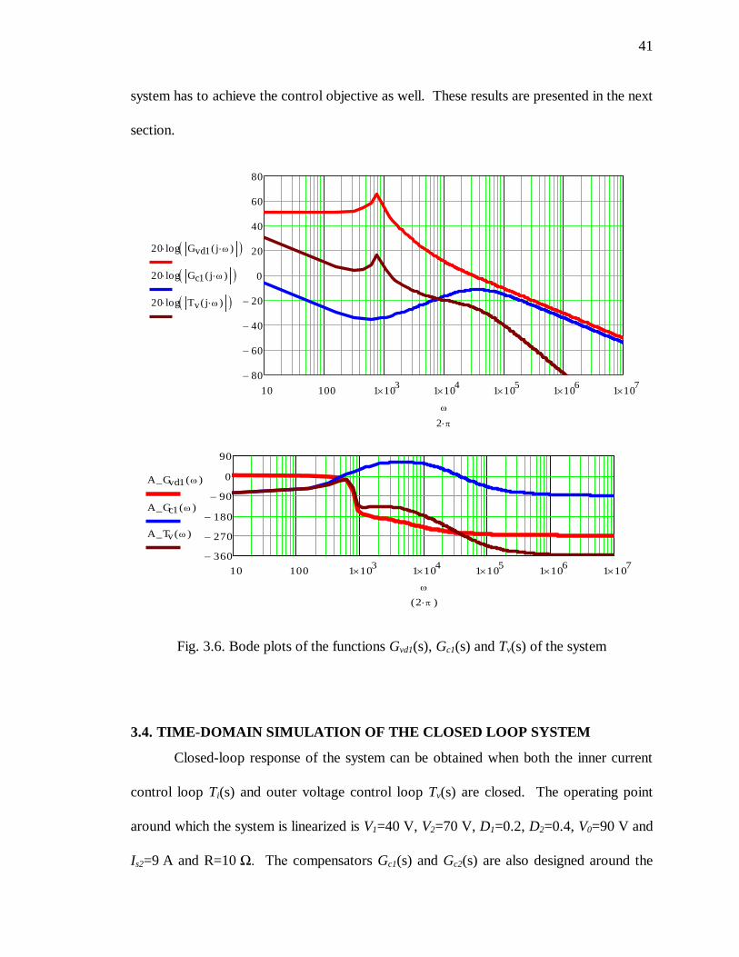
Fig. 3.6. Bode plots of the functions Gvd1(s), Gc1(s) and Tv(s) of the system
3.4. TIME-DOMAIN SIMULATION OF THE CLOSED LOOP SYSTEM
Closed-loop response of the system can be obtained when both the inner current
control loop Ti(s) and outer voltage control loop Tv(s) are closed. The operating point
around which the system is linearized is V1=40 V, V2=70 V, D1=0.2, D2=0.4, V0=90 V and
Is2=9 A and R=10 Ω. The compensators Gc1(s) and Gc2(s) are also designed around the

42
same operating point of the system. Using the compensators, a time domain simulation of
the system is carried out around the same operating point and the load is varied from 10 Ω
to 5 Ω at t=0.015 s in order to test the stability and effectiveness of the system in meeting
its control objectives. The results of the time domain simulation are shown in Figs. 3.7
3.8, and 3.9, respectively. It can be seen that output voltage V0 remains constant at 90 V
even during load variations and average switch current Is2 also remains constant at 9 A
during load variations. The additional power requirements are met by the source 1
through changes in Is1. Thus, the required control objective is effectively met through the
independent control of the two loops and proper design of Gc1(s) and Gc2(s)
compensators.
0.015 0.02 0.02560
65
70
75
80
85
90
95
100
Time (s)
V0 (
V)
Fig. 3.7. Output voltage waveform for a step change in load from 10 to 5Ω at t=0.015s
with the current and voltage loop closed with compensators Gc1(s) and Gc2(s)

43
0.015 0.02 0.0250
5
10
15
20
25
30
Time (s)
I s1 (
A)
Fig. 3.8. Average current IS1 waveforms for a step change in load from 10 to 5Ω at
t=0.015s with both loops closed
0.015 0.02 0.0258
9
10
11
12
13
14
15
Time (s)
I s2 (
A)
Fig. 3.9. Average current Is2 waveforms for a step change in load from 10 to 5Ω at
t=0.015s with both loops closed

44
So far in this thesis, the DI buckboost converter has been controlled using only
switch commands D1 and D2. In the next section, it will be proved that controlling the
delay or offset time between switch commands D1 and D2 also helps in achieving the
control objectives and improving the speed of response of the system.

45
4. OFFSET TIME CONTROL IN A DI BUCKBOOST CONVERTER
In Section 3, the closed loop control of the DI buckboost converter for the given
control objectives was achieved through the independent control of control variables D1
and D2. In this section, it is analytically proven that the offset time D12T (see Fig. 4.1) or
the delay between the switch commands can also be utilized as an additional control
variable in the closed-loop control of the converter; the actual control variables being D1
and D2. In [45], a control strategy is proposed to minimize the inductor current ripple in a
DI buck converter using D12. Offset time control has been discussed and applied to a DI
buckboost converter in [46].
In Fig. 4.1, the typical inductor current waveform for the converter is shown
where D1, D2 are the ON time duty ratios of switches S1 and S2, respectively. D12, D21 are
the offset time duty ratios or the delay between the switch commands.
D1T D12T D2T D21T
imax1
imin2
iL
t
D1+D12+D2+D21=1
imax2
T
imin1
Fig. 4.1. Inductor current waveform in the steady state operation

46
Steady-state output voltage V0 of the converter can be described as [9, 14]
)1()1( 21
22
21
110
DD
VD
DD
VDV
. (4.1)
Average inductor current IL of the converter for a resistive load R is equal to [12]
)1( 21
0
DDR
ViI LL
. (4.2)
The ratio of average switch currents is1 to is2 is defined as α
2
1
s
s
i
i
(4.3)
4.1. OFFSET TIME CONTROL SCHEME
In this section, the offset time control scheme is discussed. Alpha is proportional
to the ratio of the currents drawn from sources V1 and V2 as shown in (4.3). The amount
of power drawn from each source can thus be varied by varying α if V1 and V2 are
constant. As it will be described, α itself can be controlled by adjusting the offset time or
the delay between the switching commands (D12T or D21T in Fig. 4.1). Using the slopes of
the inductor current, the minimum inductor current imin1 can be related to imax1 by (see Fig.
4.1)
TDL
Vii 1
11max1min . (4.4)
Similarly, imin2 can be obtained from imax1 as
TDL
Vii 12
01max2min . (4.5)

47
And imax2 is related to imin2 by the following equation
TDL
Vii 2
22min2max . (4.6)
Average switch currents <is1> and <is2> are given by the following equations:
2)( 1
1min1max1
Diiis (4.7)
22 max 2 min 2( )
2s
Di i i (4.8)
From (4.5) and (4.6), it can be seen that inductor current values imax1 and imax2 are
related to each other. From (4.5), it can also be observed that imin2 is dependent on offset
time D12T. From (4.8), it can be observed that the average value of the current supplied
by V2, i.e., <is2> is dependent on imax2 and imin2 which are both in turn dependent on D12T.
Therefore, it can be concluded that by varying offset time D12T the average value of
switch currents (<is1> and <is2>) can be varied. Thus, the value of α can be varied by
varying D12T. By substituting (4.7) and (4.8) into (4.3) and by eliminating imin1, imax2, and
imin2 using (4.4), (4.5), and (4.6), eq. (4.9) can be obtained.
][
]2[
2
1
12
2
112
221220
1max
D
D
DVDVDDV
Lfi
(4.9)

48
Average inductor current <iL> can also be related to imax1 by calculating the area of
the four trapezoids in Fig. 4.1. Using (4.4), (4.5), and (4.6) this procedure leads to
])(2)([2
112022122122111max DVVDVVDDVDVD
LfiiL
(4.10)
In (4.9), a relation for imax1 in terms of α and D12 is obtained; however, imax1 needs to be
eliminated to find a relationship between D12 and α. This relationship can be obtained by
combining (4.2), (4.9), and (4.10) to eliminate imax1. The typical plot between α and D12 is
shown in Fig. 4.2 where αmin and αmax give the range in which α can be varied for the given
operating point of the converter which is determined by the value of D1 (D2 depends on D1
in order to have a constant output voltage). As shown in Fig. 4.2, the relationship
between α and D12 is almost linear and it can be observed that the ratio of power drawn
from each of the sources can be varied by varying offset time duty ratio D12 of the
converter.
D12
α
αmin
αmax
(1-D1-D2)0
Fig. 4.2. Typical plot of α vs. D12

49
4.2. CONTROL SCHEME REALIZATION
The offset time control scheme is implemented in two stages to control D12 as
shown in Figs. 4.3 and 4.4. In the first stage (see Fig. 4.3) the outer loop is regulated for
load regulation by maintaining output voltage V0 constant through the control of D1
through a voltage compensator. The average current of source 2 is held constant at Iref2
through the control of D2 through a current compensator. The value of Iref2 is based on
the energy management strategy and the control objective and is decided by an outer loop
system-level controller. In this case, the control objective is to adjust the amount of
power supplied by source 1 when the power from source 2 increases/decreases to meet
the load demand while having output voltage regulation. In other words, when reference
current Iref2 increases/decreases the average current of the other source (Is1) has to
decrease/increase accordingly to meet the load demand. For instance, in a battery/ultra-
capacitor hybrid energy system the system-level controller has to decide upon an energy
management strategy (i.e., choose a value for Iref2) based on various factors like the
battery SOC, ultra-capacitor SOC, and load demand. In this thesis, the value for Iref2 is
being externally commanded without the use of any system-level controller.
The voltage and current compensators necessary (see Fig. 4.3) for the control of
D1 and D2 have been designed in Section 3. Therefore, the offset time controller has all
the required inputs of D1, D2, and Iref2 and it should be able to vary the offset time D12
between the switch commands. In Fig. 4.4, the offset time controller block diagram is
shown. It can be realized by comparing the real value of α which is obtained at the end of
each switching cycle to αref and integrating the error to obtain the offset time duty ratio
(D12). αref can be calculated as <is1>/Iref2 as shown in Fig. 4.4 therefore, it must be noted

50
that the average switch current <is2> is being controlled through control of D2 and D12,
respectively. Finally, the PWM block (see Fig. 4.5) which has the offset time duty ratio
(D12) as an input generates the control pulses for switches S1 and S2 with a delay
proportional to the offset time D12 between them.
V1S1
is1
is2
Double-Input
Buckboost
Converter
L
o
a
dV2S2
Vref
V0
+
-
is2
is1
Iref2
D2
D1
D12
S2S1
PWM
Offset
Time
Controller
Voltage
Compensator
Current
Compensator Iref2
is2
Fig. 4.3. Block diagram of the overall system

51
Sample
& Hold
Divider
PWM
D12 S1
D1
αref= <is1>/Iref2
α
α
+
-
is2
is1
Sample
& Hold
Set
Reset
CLK
CLK
Set
Reset
K
<is1>
<is2>
Offset Time Controller
D2
αref
S2
Compensator
Compensator
Current
Voltage
<is2>
Iref2
V0
Vref
Fig. 4.4. Block diagram of the power sharing controller
S1
S2
S12
D2T
D1T
D12T
Vc_S12
Vc_S2
Sawtooth2
Sawtooth1
Fig. 4.5. Pulse width modulation block and delay D12 between S1 and S2

52
4.3. SIMULATION RESULTS FOR OPEN-LOOP RESPONSE
The DI buckboost converter with offset time controller was modeled in MATLAB
Simulink. The overall system was simulated for the following input parameters V1=40 V,
V2=70 V, V0=90 V, fs=50 kHz, L=50 µH for continuous conduction mode, and C=120 µF.
Initially the steady-state relationship between α and D12 is plotted in Fig. 4.6 for 3 different
values of D1 (0.446, 0.323, 0.2). D2 values are dependent on D1 if it is assumed that the
output voltage remains constant at 90 V. D2 values can be found by substituting all other
parameters in the steady state voltage transfer ratio given in (4.1).
From Fig. 4.6, it can be observed that the value of α increases almost linearly with
an increase in D12 when D1 and D2 are kept constant. Therefore, it can be concluded that
the ratio of the switch currents α can be controlled by controlling D12. The range in which
α can be varied depends on D1 and D2 as shown in Fig. 4.6. The average switch currents
(<is1> and <is2>)also change due to a change in D12, D1 and D2 as shown in Fig. 4.7 in
which the same set of D1, and D2 values used in Fig. 4.6 are used again. It can be
observed from Fig. 4.7 that <is1> increases with an increase in D12 and <is2> decreases
with an increase in D12. Therefore, by increasing D12, it is easier to increase average
switch current 1 <is1> when average switch current 2 <is2> is decreasing since an increase
in D12 also aids in decreasing <is2>.

53
0 0.05 0.1 0.15 0.2 0.25 0.3 0.35 0.4
0.25
0.5
0.75
1
1.25
1.5
1.75
2
2.25
2.5
2.75
3
D12
Alp
ha
()
D1=0.200, D
2=0.4, V
0=90V
D1=0.323, D
2=0.3, V
0=90V
D1=0.446, D
2=0.2, V
0=90V
a2=0.6289
a1=0.4235
Fig. 4.6. Variations of α vs. D12
0.05 0.1 0.15 0.2 0.25 0.3 0.35 0.4 0
5
10
15
D12
<i s1
>
0.05 0.1 0.15 0.2 0.25 0.3 0.35 0.44
6
8
10
D12
<i s2
>
Fig. 4.7. Variations of <is1> and <is2> vs. D12 (refer to Fig. 4.6 for markers)

54
The system is then simulated to obtain an open-loop step response for α ,i.e., a
step change in D12 from 0.10 to 0.35 occurs at t=0.015 s when D1 and D2 are kept
constant at 0.2 and 0.4, respectively. The compensators for the current and the voltage
loops are not included in the system. The value of α is expected to change from 0.4235 to
0.6289 (points a1 and a2, respectively) as predicted from the plot in Fig. 4.6. The step
response of α for a step change in D12 is shown in Fig. 4.8 which indicates a very fast
dynamics. The value of α changes almost instantaneously which indicates that the inner
loop dynamics are very fast. Therefore, controlling the input currents through the control
of the offset time would help in increasing the speed of response of the system.
0.015 0.02 0.0250.2
0.3
0.4
0.5
0.6
0.7
0.8
Time (sec)
Alp
ha
()
Fig. 4.8. Step response of α for a step change in D12 from 0.1 to 0.35

55
4.4. SMALL-SIGNAL ANALYSIS WITH OFFSET TIME CONTROL
In this section, the transfer functions are developed with the offset time control
scheme included in the model. The average switch currents Is1 and Is2 can no longer be
described by (2.10) and (2.11). The new more accurate average current equations which
are obtained from the inductor current waveform shown in Fig. 4.1 are given by
)2(2
)(2
111max
11min1max
11
Lf
DVi
Dii
DI s (4.11)
)2
2(2
)(2
221201max
22min2max
22
Lf
DV
Lf
DVi
Dii
DIs
(4.12)
Perturbing average switch current Is1, and the control variables D1, D2, and D12 in (4.11)
gives
Lf
sdDVsiisdDsiI ss
2
))(ˆ())(ˆ))((ˆ()(ˆ
2
1111max1max1111
(4.13)
It must be observed here that (4.11) seems to be a function of control variable D1 only.
However, imax1 is a function of D1, D2, and D12 as evident from (4.10). Therefore, it was
perturbed in (4.13). Neglecting the product of perturbations and equating the steady state
quantities on both sides (4.13) can be simplified to
)(ˆ]2
2[)(ˆ)(ˆ
111
1max1max11 sdLf
VDisiDsis
(4.14)
where )(ˆ1max si is obtained by perturbing (4.10)

56
))](ˆ)())((ˆ(2)))((ˆ))((ˆ(
))(ˆ())(ˆ[(2
1)(ˆ)(ˆ
12120222122211
2221111max1max
sdDVVsdDVVsdDsdD
VsdDVsdDLf
siisii LL
(4.15)
)(ˆ2
2)(ˆ
2
])(2)([
)(ˆ2
)](2[)(ˆ
2
)]([)(ˆ)(ˆ
0122
212021212
12022
11221
1max
svLf
DDsd
Lf
DVVVVDV
sdLf
VVDsd
Lf
VVDVsisi L
(4.16)
substituting (4.16) in (4.14) leads to
)(ˆ)(ˆ)(ˆ)(ˆ)(ˆ)(ˆ 12211212122111111 sv
Lf
DDDsdFsdFsdFsiDsi odsdsdsLs
(4.17)
where
Lf
VDi
Lf
VVDVDF ds
2
2
2
)]([ 111max
1221111
(4.18)
Lf
VVDVVDVDF ds
2
)](2)([ 02121212121
(4.19)
Lf
VVDDF ds
2
)](2[ 0221121
(4.20)
Using similar analysis, average switch current Is2 in perturbed form is given by
)(ˆ)(ˆ)(ˆ)()(ˆ)(ˆ 12212
202
120221max1max22 sv
Lf
DDsd
Lf
DVsd
Lf
DV
Lf
DVisiDsi os
(4.21)
Substituting (4.16) in (4.21) leads to

57
)(ˆ)1(
)(ˆ)(ˆ)(ˆ)(ˆ)(ˆ 12221212222211222 sv
Lf
DDDsdFsdFsdFsiDsi odsdsdsLs
(4.22)
where
Lf
VVDVDF ds
2
)]([ 1221212
(4.23)
Lf
DV
Lf
DVi
Lf
VVDVVDVDF ds
120221max
02121212222
2
)](2)([
(4.24)
Lf
DV
Lf
VVDDF ds
200222122
2
)](2[
(4.25)
The new set of equations (4.17) and (4.22) for )(ˆ1 sis
and )(ˆ2 sis
lead to a new
small-signal model which is shown in Fig. 4.9. It can be clearly observed from Fig. 4.9
that the switch current perturbations are functions of all the three control variables )(ˆ1 sd ,
)(ˆ2 sd , and )(ˆ
21 sd . It can also be observed that only the input side of the new small-signal
model has changed when compared to the model without offset time control shown in Fig.
2.4 and the output side has remained the same. The )(ˆ svo terms shown in (4.17) and
(4.22) are neglected in the model as the coefficients are negligible. Transfer functions
Gis1d1(s) and Gis2d2(s) derived in Section 2 as (2.24) and (2.25) will change for the model
with offset time control due to the changes in the input current dynamics in Fig. 4.9. The
new transfer functions with offset time control included can be developed from the model
shown in Fig. 4.9 and the procedure is described in the next section.

58
L
-
+
1ˆsi
1v LiD ˆ1
2ˆsi
2v LiD ˆ2
+-
-+
11vD
22vD-ovDD ˆ)1( 21 +
22ˆ)( dVV o
11ˆ)( dVV o
Li
LiDD ˆ)1( 21
)ˆˆ( 21 ddIL ov
oi
RC
222 dF ds12122 dF ds
12121 dF ds 221 dF ds 111 dF ds
112 dF ds
Fig. 4.9 Small-signal model of a DI buckboost converter with offset time control
4.5. TRANSFER FUNCTION DERIVATION WITH OFFSET TIME CONTROL
INCLUDED
In this section, the derivation of transfer function Gis1d1_offset(s) is carried out which
is the control-1 to switch current-1 transfer function when the offset time control is
included. From Fig. 4.9 and (4.17)
)(ˆ)(ˆ)(ˆ)(ˆ)(ˆ1212122111111 sdFsdFsdFsiDsi dsdsdsLs
(4.26)
In order to find transfer function Gis1d1_offset(s) one can assume 0)(ˆ2 sd in (4.26) and the
inductor current perturbations )(ˆ siLare converted into )(ˆ
1 sd by using the control-1 to
inductor current gain Gid1(s) derived earlier in Section 2 as (2.20). Furthermore, it is
assumed that the offset time control loop is closed. Therefore, )(ˆ12 sd can be replaced
with )(ˆ s by using Fig. 4.10 thereby simplifying (4.26) to
)(ˆ)(
)(ˆ)(ˆ)()(ˆ 3121
1111111 sV
sGFsdFsdsGDsi
M
cdsdsids
(4.27)

59
From Fig. 4.10, it can be observed that )(ˆ s is also dependent on )(ˆ1 sd and this
dependency is reduced by considering )(ˆ1 sd as the disturbance signal for the offset time
control loop Tα(s), once the loop is closed. Then )(ˆ s can be written as shown in (4.28)
)(ˆ)(1
)()(ˆ
)(1
)()(ˆ
1
1 sdsT
sGs
sT
sTs d
ref
(4.28)
It must be observed here that once the offset time control loop (Tα(s)) is closed then
0)(ˆ sref and (4.27) changes to
)(ˆ)(1
)()(ˆ)(ˆ)()(ˆ
1
13
1211111111 sdsT
G
V
sGFsdFsdsGDsi d
M
cdsdsids
(4.29)
12d
MV
1)(3 sGc
+- ++
1d
T
)(12 sG d
)(1 sG d
ref
Fig. 4.10 Block diagram of the converter system with the inner offset time control loop
closed
Now the transfer functions Gαd12(s) and Gαd1(s) need to be found in order to
eliminate these terms from (4.29). These relationships can be found by considering that

60
the ratio α=Is1/Is2 is controlled in offset time control. Therefore, the perturbations in
)(ˆ s are given by
2
21
122
22
11
)(ˆ)(ˆ)(ˆ
)(ˆ)(ˆ)(ˆ
)(ˆ
)(ˆ)(ˆ
s
ss
sss
ss
ss
I
sisis
sisiIs
siI
siIs
(4.30)
In order to obtain transfer function Gαd12(s), one can write )(ˆ1 sis
and )(ˆ2 sis
in terms of
control variable )(ˆ12 sd using the relations Fs1d12 and Fs2d12 obtained earlier in (4.20) and
(4.25) as
2
122121
12
12)(ˆ
)(ˆ)(
s
dsdsd
I
FF
sd
ssG
(4.31)
Using similar analysis one can also obtain the transfer function Gαd1(s) as
2
1211
1
1
)()(
)(ˆ
)(ˆ)(
s
disdisd
I
sGsG
sd
ssG
(4.32)
Therefore, the new control-1 to switch current 1 function Gis1d1_offset(s) is obtained by
substituting (4.31) and (4.32) in (4.29) leading to
)(1
)()(
)()(
)(ˆ
)(ˆ)( 2
1211
31211111
1
1_11
sT
I
sGsG
V
sGFFsGD
sd
sisG s
disdis
M
cdsdsid
soffsetdis
(4.33)
ssGc
30000)(3
(4.34)
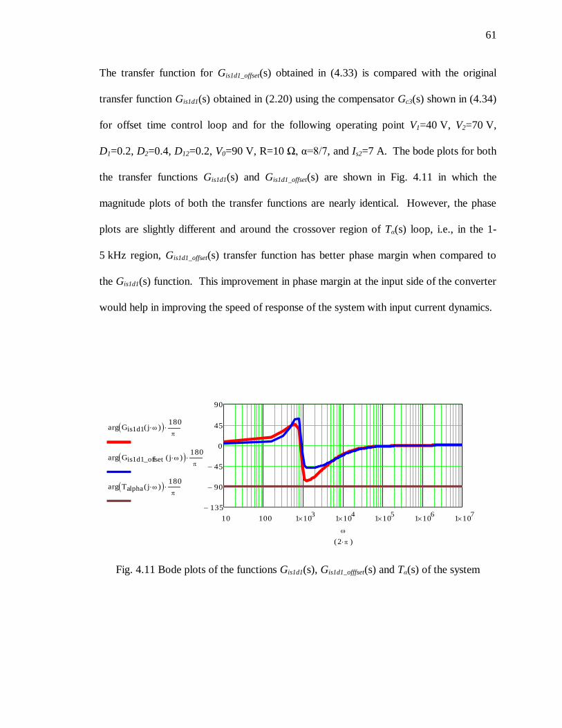
61
The transfer function for Gis1d1_offset(s) obtained in (4.33) is compared with the original
transfer function Gis1d1(s) obtained in (2.20) using the compensator Gc3(s) shown in (4.34)
for offset time control loop and for the following operating point V1=40 V, V2=70 V,
D1=0.2, D2=0.4, D12=0.2, V0=90 V, R=10 Ω, α=8/7, and Is2=7 A. The bode plots for both
the transfer functions Gis1d1(s) and Gis1d1_offset(s) are shown in Fig. 4.11 in which the
magnitude plots of both the transfer functions are nearly identical. However, the phase
plots are slightly different and around the crossover region of Tα(s) loop, i.e., in the 1-
5 kHz region, Gis1d1_offset(s) transfer function has better phase margin when compared to
the Gis1d1(s) function. This improvement in phase margin at the input side of the converter
would help in improving the speed of response of the system with input current dynamics.
10 100 1 103
1 104
1 105
1 106
1 107
135
90
45
0
45
90
arg Gis1d1 j ( ) 180
arg Gis1d1_offset j ( ) 180
arg Talpha j ( ) 180
2 ( )
Fig. 4.11 Bode plots of the functions Gis1d1(s), Gis1d1_offfset(s) and Tα(s) of the system
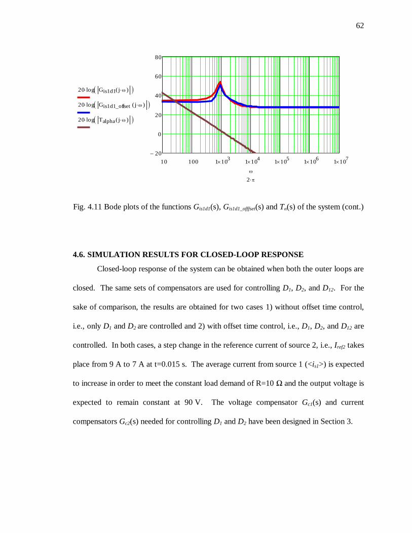
62
10 100 1 103
1 104
1 105
1 106
1 107
20
0
20
40
60
80
20 log Gis1d1 j ( )
20 log Gis1d1_offset j ( )
20 log Talpha j ( )
2
Fig. 4.11 Bode plots of the functions Gis1d1(s), Gis1d1_offfset(s) and Tα(s) of the system (cont.)
4.6. SIMULATION RESULTS FOR CLOSED-LOOP RESPONSE
Closed-loop response of the system can be obtained when both the outer loops are
closed. The same sets of compensators are used for controlling D1, D2, and D12. For the
sake of comparison, the results are obtained for two cases 1) without offset time control,
i.e., only D1 and D2 are controlled and 2) with offset time control, i.e., D1, D2, and D12 are
controlled. In both cases, a step change in the reference current of source 2, i.e., Iref2 takes
place from 9 A to 7 A at t=0.015 s. The average current from source 1 (<is1>) is expected
to increase in order to meet the constant load demand of R=10 Ω and the output voltage is
expected to remain constant at 90 V. The voltage compensator Gc1(s) and current
compensators Gc2(s) needed for controlling D1 and D2 have been designed in Section 3.

63
2
1
36780*21
311.575*21
30)(
s
s
ssGc
3
3
2
10*07.22*21
10*526.1*21
400)(
s
s
ssGc
(4.35)
The same compensators are used in this section to check the effectiveness of the
offset time control scheme. Control variable D12 is controlled through the compensator
Gc3(s) which is shown in (4.35). Output voltage V0 and the average current waveforms of
both the switches (<is1> and <is2>) with and without offset time (D12) control are shown in
Figs. 4.12, 4.13 and 4.14, respectively. It can be clearly observed from Fig. 4.12 that the
output voltage reaches the steady state value of 90 V much faster and has less overshoot
when the offset time control is applied. It can also be observed from Figs. 4.13 and 4.14
that the average switch currents (<is1> and <is2>) also settle to their new steady state
values much faster when the offset time control scheme is applied. Therefore, offset time
control scheme increases the speed of response of the system when the input currents of
the DI buckboost converter are varying. This is very common in hybrid energy systems.

64
0.015 0.02 0.02570
75
80
85
90
95
100
Time (sec)
V0 (
V)
V0 with D
12 control
V0 without D
12 control
Fig. 4.12. Output voltage V0 waveforms with and without D12 control for a step change in
Iref2 from 9 to 7 A
0.015 0.02 0.0252
3
4
5
6
7
8
9
10
Time (sec)
<i s1
> (
A)
Is1
with D12
control Is1
without D12
control
Fig. 4.13. Average current of source 1 <is1> waveforms with and without D12 control for
a step change in Iref2 from 9 to 7 A

65
0.015 0.02 0.0255
5.5
6
6.5
7
7.5
8
8.5
9
9.5
10
Time (sec)
<i s2
> (
A)
Is2
with D12
control
Is2
without D12
control
Fig. 4.14. Average current of source 2 <is2> waveforms with and without D12 control for
a step change in Iref2 from 9 to 7 A
4.7. CONCLUSION
Offset time control scheme is introduced and applied to a DI buckboost converter.
It is theoretically proven that adjusting the offset time between the switch commands has a
direct impact on the current drawn from each source. Offset time can be used as an
additional control variable in systems with input current dynamics. Offset time control is
very useful in situations like partial shading for a grid/solar combination or low ultra-
capacitor SOC for a battery/ultra-capacitor combination where the average current
supplied by the PV array or the ultra-capacitor is decreasing and the average current
supplied by the other source has to increase to meet the load demand. In such situations,
the ratio between the source currents is rapidly changing and controlling this ratio through
a proportional control variable (offset time) would help in improving the dynamic
performance of the system while the control objectives are achieved.

66
5. CONCLUSION
In this thesis, the control of DI buckboost converter is discussed. A small-signal
model for the DI buckboost converter is developed and the compensator design is carried
out for the system. Two compensators are designed to meet the control objective of
supplying constant power from one source (PV) and meeting the additional load demand
through the other source (battery) during load variations. It is analytically proven that the
control objective can be achieved by independent control of the two loops controlling the
two switches. This independent control of the two loops simplifies the compensator
design procedure. Therefore, the compensators for the two loops are designed
independently; one to maintain output voltage regulation and another to maintain switch
current from source 2 constant. The closed-loop system is tested for load regulation using
the designed compensators. The system is stable and has a good dynamic response. Apart
from the small-signal modeling a new control method called the offset time control is also
introduced and successfully applied to a DI buckboost converter in this thesis. The
control scheme is based on adjusting the offset time between the switching commands
which is proven to have a direct impact on the amount of current drawn from each input.
This devised control method is fixed frequency and provides an extra degree of freedom in
power sharing. The proposed control method has a very fast dynamic response, improves
the stability of traditional controllers, and meets the control objectives better. The analysis
can be extended to other DIPEC topologies which are used for the integration of various
renewable energy sources.
67
BIBLIOGRAPHY
[1] H. Li, Z. Du, K. Wang, L. M. Tolbert, and D. Liu, “A hybrid energy system using
cascaded H-bridge converter,” in Proc. IEEE Industrial Applications Conf., vol. 1,
Oct. 2006, pp.198-203.
[2] L. Solero, F. Caricchi, F. Crescimbini, O. Honorati, and F. Mezzetti, “Performance
of a 10 kW power electronic interface for combined wind/PV isolated generating
systems,” in Proc. IEEE Power Electronics Specialists Conf. (PESC), Jun. 1996,
vol. 2, pp. 1027–1032.
[3] A. D. Napoli, F. Crescimbini, S. Rodo, and L. Solero, “Multiple input dc-dc power
converter for fuel-cell powered hybrid vehicles”, in Proc. IEEE Power Electronics
Specialists Conf. (PESC), Jun. 2002, vol. 4, pp. 1685–1690.
[4] R. M. Schupbach, J. C. Balda, M. Zolot, and B. Kramer, “Design methodology of a
combined battery-ultracapacitor energy storage unit for vehicle power management,”
in Proc. IEEE Power Electronics Conf., 15-19 Jun. 2003, vol. 1, pp. 88-93.
[5] Y. M. Chen, Y. C. Liu, and F. Y. Wu, “Multi-input converter with power factor
correction, maximum power point tracking, and ripple-free input currents,” IEEE
Trans. Power Electronics, vol. 19, pp. 631-639, May 2004.
[6] Y. M. Chen, Y. C. Liu, F. Y. Wu, and Y. E. Wu, “Multi-input converter with power
factor correction and maximum power point tracking features,” in Proc. IEEE
Applied Power Electronics Conf. and Exposition (APEC), vol. 1, Mar. 2002, pp.
490-496.
[7] H. Tao, A. Kotsopoulos, J. L. Duarte, and M. A. M. Hendrix, “Family of multiport
bidirectional dc-dc converters,” in Proc. IEEE Electric Power Applications, vol.
153, May 2006, pp. 451 - 458.
[8] H. Tao, A. Kotsopoulos, J. L. Duarte, and M. A. M. Hendrix, “Triple-half-bridge
bidirectional converter controlled by phase shift and PWM,” in Proc. IEEE Applied
Power Electronics Conf. and Exposition (APEC), Dallas, TX, USA, Mar. 2006, pp.
1256-1262.
[9] K. P. Yalamanchili, M. Ferdowsi, and K. Corzine, “New double input dc-dc
converter for automotive applications,” in Proc. IEEE Vehicle Power and
Propulsion Conf., 6-8 Sept. 2006, pp 1-6.
[10] K. P. Yalamanchili and M. Ferdowsi, “Review of multiple input DC-DC converters
for electric and hybrid vehicles,” in Proc. IEEE Vehicle Power and Propulsion
Conf., 7-9 Sept. 2005, pp. 160-163.

68
[11] Y. M. Chen and Y. C. Liu, “Development of multi-port converters for hybrid wind-
photovoltaic power system,” in Proc. IEEE Region 10 International Conf. on
Electrical and Electronic Technology, vol.2, Aug. 2001, pp. 804-808.
[12] K. P. Yalamanchili, “Multi-input dc-dc converters for combined energy storage
systems in hybrid electric vehicles,” M. S. Thesis, University of Missouri-Rolla, Dec.
2006.
[13] K. Gummi, “Derivation of new double-input dc-dc converters using Building Block
Methodology,” M. S. Thesis, University of Missouri-Rolla, Dec. 2006.
[14] K. Gummi and M. Ferdowsi, “Synthesis of double-input dc-dc converters using
single pole triple throw switch as a building block,” in Proc. IEEE Power
Electronics Specialists Conf. (PESC), Greece, Jun. 2008.
[15] K. Gummi and M. Ferdowsi, “Derivation of new double-input converters using H-
Bridge cells as Building Blocks,” in Proc. IEEE Industrial Electronics Conf.,
Orlando, FL, USA, November 2008.
[16] B. G. Dobbs and P. L. Chapman, “A multiple-input dc-dc converter topology,”
IEEE Power Electronics Letters, vol. 1, pp. 6-9, Mar. 2003.
[17] S. H. Choung and A. Kwasinki, “Multi-input dc-dc converter topologies
comparison,” in Proc. IEEE Industrial Electronics Conf. (IECON), Nov. 2008, pp.
2359-2364.
[18] N. D. Benavides and P. L. Chapman, “Object-oriented modeling of a multiple-input
multiple-output flyback converter in Dymola,” in Proc. IEEE workshop on
Computer Power Electronics, 15-18 Aug. 2004, pp. 150-160.
[19] Y. C. Liu and Y. M. Chen, “A systematic approach to synthesizing multi-input dc/dc
converters,” in Proc. IEEE Power Electronics Specialists Conf. (PESC), Jun. 2007,
pp. 2626-2632.
[20] Y. M. Chen, Y. C. Liu, S. C. Hung, and C. S. Cheng, “Multi-input inverter for grid-
connected hybrid pv/wind power system,” in Proc. IEEE Trans. Power Electronics,
vol. 22, pp. 1070-1077, May 2007.
[21] N. D. Benavides and P. L. Chapman, “Power budgeting of a multiple-input buck-
boost converter,” IEEE Trans. Power Electronics, vol. 20, pp. 1303-1309, Nov.
2005.
[22] N. D. Benavides, T. Esram and P. L. Chapman, “Ripple correlation control of a
multiple-input dc-dc converter,” in Proc. IEEE Power Electronics Specialists Conf.
(PESC), Jun. 2005, pp. 160-164.
69
[23] Y. M. Chen, Y. C. Liu, and S. H. Lin, “Double-input pwm DC/DC converter for
high/low-voltage sources,” IEEE Trans. Industrial Electronics, vol. 53, pp. 1538-
1545, Oct. 2006.
[24] Y. M. Chen, Y. C. Liu, and F. Y. Wu, “Multi-input DC/DC converter based on the
multiwinding transformer for renewable energy applications,” IEEE Trans. Industry
Applications., vol.38, pp. 1096-1104, Aug. 2002.
[25] Y. M. Chen, C. S. Cheng, and H. C. Wu, “Grid-connected hybrid PV/wind power
generation system with improved DC bus voltage regulation strategy,” in Proc.
IEEE Applied Power Electronics Conf. (APEC), Mar. 2006, pp. 1088-1094.
[26] A. Di Napoli, F. Crescimbini, L. Solero, F. Caricchi, and F. G. Capponi, “Multiple-
input dc-dc power converter for power-flow management in hybrid vehicles,” in
Proc. Rec. 37th Annu. IEEE Industry Applications Conf., 2002, pp. 1578–1585.
[27] A. Khaligh, J.Ciao and Y. J. Lee, “A Multiple-input dc-dc converter topology,”
IEEE Power Electronic Letters, vol. 24, pp. 862-868, Mar 2009.
[28] R. W. Erickson and D. Maksimovic, Fundamentals of Power Electronics, 2nd ed.
Norwell, M. A. Kluwer, 2001.
[29] J. G. Kassakian, M. F. Schlecht, and G. C. Verghese, Principles of Power
Electronics, 2nd ed, Addison Wesley, 1991.
[30] J. Rajagopalan, K. Xing, Y. Guo, F. C. Lee and B. Manners, “Modeling and
dynamic analysis of paralleled dc/dc converters with master-slave current sharing
control,” in Proc. IEEE Applied Power Electronics Conf. (APEC), Mar. 1996, pp.
678-684.
[31] B. Choi, B. H. Cho, R. B. Ridley and F. C. Lee “Control Strategy for multi-module
parallel converter system,” in Proc. IEEE Power Electronic Specialists Conf.
(PESC), Jun 1990, pp. 225-234.
[32] S. Angkititrakul, H. Hu and Z. Liang, “Active inductor current balancing for
interleaving multi-phase buck-boost converter,” in Proc. IEEE Applied Power
Electronics Conf. (APEC), Feb. 2009, pp. 527-532.
[33] W. Tang, F. C. Lee, R. B. Ridley and I. Cohen “Charge Control: Modeling,
Analysis, and Design,” IEEE Trans. Power Electronics, vol. 8, pp.396-403, Oct.
1993.
[34] B. H. Cho and F. C. Lee “Measurement of loop gain with digital modulator,” in
Proc. IEEE Trans. Power Electronics, vol. 8, pp. 112-119, Apr 1993.
70
[35] R. B. Ridley, B. H. Cho and F. C. Lee, “Analysis and interpretation of loop gains of
multiloop-controlled switching regulators,” IEEE Trans. on Power Electronics, vol.
3, pp. 489-498, Oct. 1988.
[36] L. H. Dixon, “Average current-mode control of switching power supplies,” in
Unitrode Power Supply Design and Seminar Handbook, 1990.
[37] W. Tang, R. B. Ridley and F. C. Lee “Small-signal modeling of average current-
mode control,” in Proc. IEEE Trans. Power Electronics, vol. 8, pp. 55-62, Jan.
1986.
[38] S. M. Khazraei, A. Rahmati and A. Abrishamifar, “Fuzzy-linear control of an input-
series and output-parallel dc-dc converter,” in Proc. IEEE International Conference
on Industrial Technology, 21-24 Apr. 2008, pp. 1-5.
[39] S. M. Khazraei, A. Rahmati and A. Abrishamifar, “Small signal and large signal
charge control models for a phase-shifted PWM converter,” in Proc. IEEE
International Conference on Industrial Technology, 21-24 Apr. 2008, pp. 1-6.
[40] R. Ayyanar, R. Giri and N. Mohan, “Active input-voltage and load-current sharing in
input-series and output-parallel connected modular dc-dc converters using dynamic
input-voltage reference scheme,” IEEE Trans. Power Electronics, vol. 19, pp.1462-
1473, Nov 2004.
[41] L.H. Dixon, "Closing the Feedback Loop", Appendix C, Unitrode Power Supply
Design Seminar, pp.2C1-2C18, 1983
[42] http://dataweek.co.za/news.aspx?pklNewsId=31635&pklCategoryID=46 Loop
compensation of voltage-mode boost converters (last accessed on August 21, 2009).
[43] H. Dean Venable, “The k-factor: a new mathematical tool for stability analysis and
synthesis,” in Proc. Power Con 10, San Diego, CA, March 22-24, 1983.
[44] W. H. Lei and T. K. Man, “A general approach for optimizing dynamic response of a
buck converter,” in Proc. Application notes Onsemi Conductors, Document id
AND8143/D.
[45] Y. Li, Y. Dongsheng, and R. Xinbo, “Interleaved dual-edge modulation scheme for
double-input converter to minimize inductor current ripple,” in Proc. IEEE Power
Electronics Specialists Conference (PESC), 15-19 Jun. 2008, pp.1783 – 1789.
[46] D. Somayajula and M. Ferdowsi, “Power sharing in a double-input buckboost
converter using offset time control,” in Proc. IEEE Applied Power Electronics
Conf. (APEC), Feb. 2009, pp. 1091-1096.

71
VITA
Deepak Balaji Somayajula was born on 5th March, 1984. He graduated from
Pondicherry University (India) with a BSEE degree in 2005. He had been working as a
Software Engineer at Infosys Technologies, India from 2005 to 2007. He started his
MSEE degree at Missouri University of Science and Technology (Rolla) in August 2007
and graduated in December 2009. His main research interest is modeling and control of
multi-input dc-dc power electronic converters. His other research interests include design
and sizing of energy management systems for PHEVs and power electronics integration
into power systems.

![[1]Oracle® Fusion Middleware Oracle Cloud Adapter for ... · Srikanth Somayajula, Venkata Purna Vamsi Krishna Jandhyala, Rajesh Venkataraman, Divya Vijayalakshmi This software and](https://static.fdocuments.in/doc/165x107/5f0bf3827e708231d4330682/1oracle-fusion-middleware-oracle-cloud-adapter-for-srikanth-somayajula.jpg)