Contents - web.stanford.eduweb.stanford.edu/class/ee152/resources/main020312.pdf · C.5 Current...
165
Contents 1 Introduction: The World Needs Green Electronics 5 1.1 The Energy Crisis .......................... 5 1.2 Green Electronics: Part of the Solution .............. 6 1.2.1 Example 1: Photovoltaic Generation ............ 6 1.2.2 Example 2: An Electric Car ................. 8 1.3 The World Needs More Green Engineers .............. 10 1.3.1 What you will learn ..................... 10 1.3.2 Learn By Doing ....................... 11 1.3.3 Prerequisites ......................... 11 1.4 Bibliographic Notes .......................... 12 2 Build an Energy Meter 13 2.1 Hardware ............................... 13 2.2 Software ................................ 16 2.2.1 Sensing Software ....................... 17 2.3 The Lab ................................ 19 2.4 Extensions ............................... 20 3 Motor Controller 23 3.1 Motor Model ............................. 24 3.2 Power Path .............................. 27 3.3 Regenerative Braking ........................ 31 3.4 Matlab Simulation .......................... 32 3.5 Controller ............................... 36 3.6 The Lab ................................ 38 3.7 Extensions ............................... 39 4 Battery Charger 41 4.1 Modeling a Battery .......................... 41 4.2 Charging Sequence .......................... 42 4.3 Power Path of the Charger ..................... 44 4.3.1 Input Stage .......................... 44 4.3.2 Switching Stage and Output Filter ............. 47 4.4 Control of the Charger ........................ 49 1
Transcript of Contents - web.stanford.eduweb.stanford.edu/class/ee152/resources/main020312.pdf · C.5 Current...

Contents
1 Introduction: The World Needs Green Electronics 51.1 The Energy Crisis . . . . . . . . . . . . . . . . . . . . . . . . . . 51.2 Green Electronics: Part of the Solution . . . . . . . . . . . . . . 6
1.2.1 Example 1: Photovoltaic Generation . . . . . . . . . . . . 61.2.2 Example 2: An Electric Car . . . . . . . . . . . . . . . . . 8
1.3 The World Needs More Green Engineers . . . . . . . . . . . . . . 101.3.1 What you will learn . . . . . . . . . . . . . . . . . . . . . 101.3.2 Learn By Doing . . . . . . . . . . . . . . . . . . . . . . . 111.3.3 Prerequisites . . . . . . . . . . . . . . . . . . . . . . . . . 11
1.4 Bibliographic Notes . . . . . . . . . . . . . . . . . . . . . . . . . . 12
2 Build an Energy Meter 132.1 Hardware . . . . . . . . . . . . . . . . . . . . . . . . . . . . . . . 132.2 Software . . . . . . . . . . . . . . . . . . . . . . . . . . . . . . . . 16
2.2.1 Sensing Software . . . . . . . . . . . . . . . . . . . . . . . 172.3 The Lab . . . . . . . . . . . . . . . . . . . . . . . . . . . . . . . . 192.4 Extensions . . . . . . . . . . . . . . . . . . . . . . . . . . . . . . . 20
3 Motor Controller 233.1 Motor Model . . . . . . . . . . . . . . . . . . . . . . . . . . . . . 243.2 Power Path . . . . . . . . . . . . . . . . . . . . . . . . . . . . . . 273.3 Regenerative Braking . . . . . . . . . . . . . . . . . . . . . . . . 313.4 Matlab Simulation . . . . . . . . . . . . . . . . . . . . . . . . . . 323.5 Controller . . . . . . . . . . . . . . . . . . . . . . . . . . . . . . . 363.6 The Lab . . . . . . . . . . . . . . . . . . . . . . . . . . . . . . . . 383.7 Extensions . . . . . . . . . . . . . . . . . . . . . . . . . . . . . . . 39
4 Battery Charger 414.1 Modeling a Battery . . . . . . . . . . . . . . . . . . . . . . . . . . 414.2 Charging Sequence . . . . . . . . . . . . . . . . . . . . . . . . . . 424.3 Power Path of the Charger . . . . . . . . . . . . . . . . . . . . . 44
4.3.1 Input Stage . . . . . . . . . . . . . . . . . . . . . . . . . . 444.3.2 Switching Stage and Output Filter . . . . . . . . . . . . . 47
4.4 Control of the Charger . . . . . . . . . . . . . . . . . . . . . . . . 49
1

2 Green Electronics Class Notes
4.4.1 Layered Control . . . . . . . . . . . . . . . . . . . . . . . 494.4.2 State Machine . . . . . . . . . . . . . . . . . . . . . . . . 504.4.3 Buck Regulator . . . . . . . . . . . . . . . . . . . . . . . . 514.4.4 PWM Current-Mode Control . . . . . . . . . . . . . . . . 51
4.5 Simulation . . . . . . . . . . . . . . . . . . . . . . . . . . . . . . . 554.6 Software . . . . . . . . . . . . . . . . . . . . . . . . . . . . . . . . 574.7 Circuit Simulation . . . . . . . . . . . . . . . . . . . . . . . . . . 604.8 The Lab . . . . . . . . . . . . . . . . . . . . . . . . . . . . . . . . 694.9 Extensions . . . . . . . . . . . . . . . . . . . . . . . . . . . . . . . 69
5 Build a Photovoltaic Controller 735.1 Photovoltaic Panel . . . . . . . . . . . . . . . . . . . . . . . . . . 735.2 Power Path . . . . . . . . . . . . . . . . . . . . . . . . . . . . . . 755.3 Controller . . . . . . . . . . . . . . . . . . . . . . . . . . . . . . . 765.4 Matlab Simulation . . . . . . . . . . . . . . . . . . . . . . . . . . 765.5 SPICE Simulation . . . . . . . . . . . . . . . . . . . . . . . . . . 815.6 The Laboratory . . . . . . . . . . . . . . . . . . . . . . . . . . . . 835.7 Extensions . . . . . . . . . . . . . . . . . . . . . . . . . . . . . . . 83
A Safety 87A.1 Risks . . . . . . . . . . . . . . . . . . . . . . . . . . . . . . . . . . 87A.2 Rules and Procedures . . . . . . . . . . . . . . . . . . . . . . . . 88
B Processor Module 91B.1 Schematic . . . . . . . . . . . . . . . . . . . . . . . . . . . . . . . 91B.2 Software . . . . . . . . . . . . . . . . . . . . . . . . . . . . . . . . 93
B.2.1 Display and Switch Input . . . . . . . . . . . . . . . . . . 93B.2.2 Real-Time Clock Interrupt . . . . . . . . . . . . . . . . . 94B.2.3 Analog Input . . . . . . . . . . . . . . . . . . . . . . . . . 95B.2.4 PWM . . . . . . . . . . . . . . . . . . . . . . . . . . . . . 95B.2.5 Calibration . . . . . . . . . . . . . . . . . . . . . . . . . . 96B.2.6 Filtering . . . . . . . . . . . . . . . . . . . . . . . . . . . . 96
C Component Module 99C.1 Current Sense Resistor . . . . . . . . . . . . . . . . . . . . . . . . 99C.2 Inductor . . . . . . . . . . . . . . . . . . . . . . . . . . . . . . . . 100C.3 Diode . . . . . . . . . . . . . . . . . . . . . . . . . . . . . . . . . 101C.4 Capacitor . . . . . . . . . . . . . . . . . . . . . . . . . . . . . . . 101C.5 Current Transformer . . . . . . . . . . . . . . . . . . . . . . . . . 102C.6 AC Input Circuit . . . . . . . . . . . . . . . . . . . . . . . . . . . 102
D Half-Bridge Module 105D.1 Power MOSFETs . . . . . . . . . . . . . . . . . . . . . . . . . . . 105D.2 MOSFET Drivers . . . . . . . . . . . . . . . . . . . . . . . . . . . 107
Copyright (c) 2011 by W.J Dally, all rights reserved 3
E Buck Module 109E.1 Circuit Measurements and Subtleties . . . . . . . . . . . . . . . . 109
E.1.1 Measurements . . . . . . . . . . . . . . . . . . . . . . . . 109E.1.2 Input Snubber . . . . . . . . . . . . . . . . . . . . . . . . 114E.1.3 Overlap Current . . . . . . . . . . . . . . . . . . . . . . . 114
F Motor and Battery Cart 115
G Project Ideas 117
H Circuit Theory 119H.1 Voltage, Current, and Power . . . . . . . . . . . . . . . . . . . . . 119H.2 Resistors and Ohm’s Law . . . . . . . . . . . . . . . . . . . . . . 121H.3 Kirchoff’s Laws . . . . . . . . . . . . . . . . . . . . . . . . . . . . 122H.4 Examples . . . . . . . . . . . . . . . . . . . . . . . . . . . . . . . 124
H.4.1 Series Resistors and Voltage Dividers . . . . . . . . . . . . 124H.4.2 Parallel Resistors and Current Dividers . . . . . . . . . . 125H.4.3 Combined Series Parallel Circuit . . . . . . . . . . . . . . 126H.4.4 Thevenin and Norton Equivalents . . . . . . . . . . . . . 128
H.5 Linearity and Superposition . . . . . . . . . . . . . . . . . . . . . 129
I Capacitors and RC Circuits 131I.1 Capacitors . . . . . . . . . . . . . . . . . . . . . . . . . . . . . . . 131I.2 RC Circuits . . . . . . . . . . . . . . . . . . . . . . . . . . . . . . 132I.3 Impulse Response and Step Response . . . . . . . . . . . . . . . . 132
J Inductors, LR, and LC Circuits 133
K Operational Amplifiers 135K.1 Model . . . . . . . . . . . . . . . . . . . . . . . . . . . . . . . . . 135K.2 OpAmp Circuits . . . . . . . . . . . . . . . . . . . . . . . . . . . 135K.3 OpAmp and Capacitor Circuits . . . . . . . . . . . . . . . . . . . 138K.4 Real OpAmps . . . . . . . . . . . . . . . . . . . . . . . . . . . . . 138K.5 Exercises . . . . . . . . . . . . . . . . . . . . . . . . . . . . . . . 140
L Real Circuit Elements 141L.1 Resistors . . . . . . . . . . . . . . . . . . . . . . . . . . . . . . . . 141L.2 Inductors . . . . . . . . . . . . . . . . . . . . . . . . . . . . . . . 141L.3 Capacitors . . . . . . . . . . . . . . . . . . . . . . . . . . . . . . . 141L.4 Transformers . . . . . . . . . . . . . . . . . . . . . . . . . . . . . 141L.5 Standard Values . . . . . . . . . . . . . . . . . . . . . . . . . . . 141L.6 Cost Model . . . . . . . . . . . . . . . . . . . . . . . . . . . . . . 141

4 Green Electronics Class Notes
M Switches 143M.1 Metal-Oxide-Semiconductor Field Effect Transistor (MOSFET) . 143M.2 Insulated-Gate Bipolar Transistors . . . . . . . . . . . . . . . . . 143M.3 Diodes . . . . . . . . . . . . . . . . . . . . . . . . . . . . . . . . . 144M.4 Silicon Controller Rectifiers (SCRs) . . . . . . . . . . . . . . . . . 144M.5 Driver circuits . . . . . . . . . . . . . . . . . . . . . . . . . . . . . 144M.6 Isolation . . . . . . . . . . . . . . . . . . . . . . . . . . . . . . . . 144
N Feedback Control 145N.1 Basic Principles . . . . . . . . . . . . . . . . . . . . . . . . . . . . 145N.2 First Order System . . . . . . . . . . . . . . . . . . . . . . . . . . 148N.3 Second-Order System . . . . . . . . . . . . . . . . . . . . . . . . 152N.4 Controlling a Buck Converter . . . . . . . . . . . . . . . . . . . . 155
N.4.1 Voltage-Mode Control . . . . . . . . . . . . . . . . . . . . 155N.4.2 Current-Mode Control . . . . . . . . . . . . . . . . . . . . 156
N.5 Frequency Response of Controllers . . . . . . . . . . . . . . . . . 158
O SPICE Simulation 163O.1 A Simple Example . . . . . . . . . . . . . . . . . . . . . . . . . . 163O.2 Basic Circuit Elements . . . . . . . . . . . . . . . . . . . . . . . . 163O.3 Subcircuits . . . . . . . . . . . . . . . . . . . . . . . . . . . . . . 163O.4 Models and Libraries . . . . . . . . . . . . . . . . . . . . . . . . . 163O.5 Sources . . . . . . . . . . . . . . . . . . . . . . . . . . . . . . . . 163O.6 Measurement Statements . . . . . . . . . . . . . . . . . . . . . . 163O.7 A Detailed Example . . . . . . . . . . . . . . . . . . . . . . . . . 163
Chapter 1
Introduction: The WorldNeeds Green Electronics
1.1 The Energy Crisis
An increasing, industrialized world population is putting undue pressures on ourworld’s delicate ecosystem and on our natural resources. In the United States,85% of energy generated is from fossil fuels (DOE Annual Energy Outlook).While there are large reserves, that are increasing as people get better at ex-ploration and recovery, the supply is finite. We will ultimately run out of fossilfuels.
Even if our supply of fossil fuels was infinite, burning fossil fuels generatesgreenhouse gasses like CO2 that accumulate in the atmosphere leading to climatechange. In recent years, atmospheric CO2 has been increasing at a rate of about20ppm/decade (5% per decade) (NOAA data). We need to burn less fossil fuels,or sequester the carbon generated by burning these fuels, or both — or sufferthe consequences of climate change.
To deal both with the limited supplies of fossil fuels and their environmentalimpact, we need to develop technologies for economic renewable energy sources.Wind and solar power are two of the most promising candidates — both dependstrongly on green electronics. Photovoltaic controllers, generator controllers,and inverters are important components in efficiently getting energy from solarcells and windmills to the grid — and ultimately to the end user.
Conservation plays a large role in reducing our consumption of fossil fuelsand our generation of greenhouse gasses. Replacing inefficient incandescentlamps with highly-efficient LED lamps and using intelligent control to havelamps only illuminate areas where people are looking can dramatically reducethe energy consumption due to lighting. Data centers, which consume about2% of the electric power in the US, use power supplies that are often only 70-80% efficient and processors that spend the bulk of their power on overhead.More efficient power supply and processor design woudl dramatically reduce
5
6 Green Electronics Class Notes
electricity consumption. There are many more examples where efficient powerelectronics and intelligent control can greatly reduce consumption.
1.2 Green Electronics: Part of the Solution
A key technology for both sustainable energy generation and conservation isthe combination of intelligent control with power electronics — the brains andbrawn of energy systems. The power electronics provides the brawn — doingthe heavy work of converting energy from one form to another. This includeselectrical conversion — as in a photovoltaic system where the DC output voltagefrom a string of solar panels is converted to AC power at a different voltage todrive the grid — and mechanical conversion where the system includes a motoror generator — as in a wind farm or an electric vehicle.
Intelligent computer control provides the brains of the system, optimizingoperation to improve efficiency. A photovoltaic controller searches to find theoptimum operating point for each solar cell in a string — optimizing efficiency.A controller electrically switches the windings of a brushless generator on a windmill, achieving greater efficiency than with an alternator or a generator with acommutator. A lighting controller uses cameras to sense the location and gazeof people in a building to turn on lights only where they are needed.
1.2.1 Example 1: Photovoltaic Generation
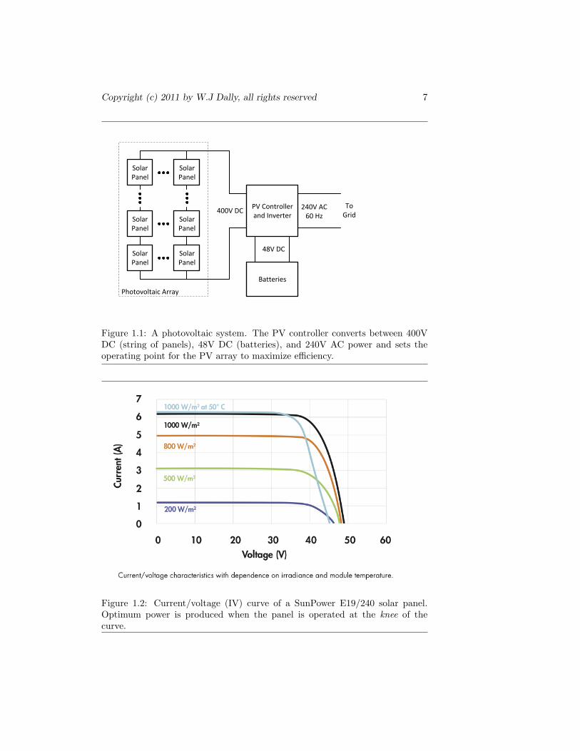
As an example of a green-electronics system, consider the grid-connected photo-voltaic system of Figure 1.1. A photovoltaic (PV) array of solar panels convertssolar energy to electricity. With a typical configuration of 10 40V panels ineach series string, the output of this array is 400V DC. The power depends onthe number of strings and for a residential system is typically in the range of4-10kW. So the DC current out of the PV array is in the rane of 10-25A.
A PV Controller and Inverter connects the PV array to a bank of batteries(that operate at 48V DC) and to the electric grid (240V AC). The PV controllerconverts electrical energy from one form to another. For a 4kW system, itconverts 10A at 400V DC to 16.7A at 240V AC to drive the grid, or to 83.3Aat 48V DC to charge the batteries.
The controller also sets the operating point of the PV array to maximizethe energy produced. As shown in Figure 1.2, a solar panel acts as a currentsource — producing a nearly constant current up until a maximum voltagewhere the current falls quickly. To get maximum power out of the panel, itmust be operated at the knee of this curve — at the voltage where the currentjust begins to drop. The PV controller adjusts its output impedance to operatethe array at this point.
Because of non-uniformity of illumination and manufacturing not all panelsmay have the same opimal operating point. In a simple system like that shown inFigure 1.1 the controller must set a single operating point that is a compromise— it gives the highest power over all but may not be the best for each panel.
Copyright (c) 2011 by W.J Dally, all rights reserved 7
Solar Panel
Solar Panel
Solar Panel
Solar Panel
Solar Panel
Solar Panel
Photovoltaic Array
PV Controller and Inverter
Batteries
400V DC 240V AC60 Hz
48V DC
To Grid
Figure 1.1: A photovoltaic system. The PV controller converts between 400VDC (string of panels), 48V DC (batteries), and 240V AC power and sets theoperating point for the PV array to maximize efficiency.
Figure 1.2: Current/voltage (IV) curve of a SunPower E19/240 solar panel.Optimum power is produced when the panel is operated at the knee of thecurve.

8 Green Electronics Class Notes
Charger120/240V AC60 Hz
From Grid
Battery
Battery
Battery
Battery Pack
400V DCMotor
Controller
AC Induction or Brushless PM Motor
400V DC
3-phase ACVariable Voltage
Variable Frequency
Resistive Load
User Interface
Figure 1.3: Block diagram of an electric car. Energy is stored in a centralbattery pack that can be charged from the grid when the car is parked. Acontroller can transfer energy in either direction between the battery pack andan electric motor.
More sophisticated PV controllers monitor the voltage and current acrosseach panel independently and by bypassing current around some panels (usinga switched-inductor shunt) operate every panel at its peak power point.
In a grid-connected system that includes battery storage, an intelligent con-troller decides when to charge the batteries to make best use of time-of-daypower rates. It will charge the batteries during off-peak times when electricityis substantially cheaper than during peak times1. Not only does this optimizeeconomics, it also optimizes efficiency because the peaking plants used by theelectric utility to provide power at peak times are substantially less efficientthan the plants used to provide base capacity.
The controller will also tailor the charging profile to maximize efficiency andbattery life. A sophisticated controller will monitor the voltage of individualbattery cells and balance the cells to optimize operation.
We will take a closer look at aspects of this model PV system in the labs thatmake up the bulk of this course. In Chapter 5 we investigate solar panels andbuild a photovoltaic controller for a single solar panel and develop an algorithmfor operating at the peak power point. We examine the properties of batteriesand build a battery charger in Chapter 4.
1.2.2 Example 2: An Electric Car
A second example of a green electronics system is the electric car of Figure 1.3.The electronics here charge and manage the batteries and control the motorthat provides vehicle propulsion.
When the car is parked, a charger converts 120V or 240V AC power to 400VDC power to charge the battery pack. While individual battery cells range from
1Under the California E-7 Tariff, the peak rate is nearly four times the off-peak rate.

Copyright (c) 2011 by W.J Dally, all rights reserved 9
2V (lead-acid) to 3.7V (Lithium ion), hundreds of these cells are connected inseries to give an efficient operating voltage of 400V DC. The charger mustcarefully manage voltage, current, and temperature during the charging processto maximize efficiency and battery life.
The motor controller converts the 400V DC voltage to a three-phase ACvoltage to drive the motor. The frequency of the motor drive depends on themotor speed. The effective voltage of the motor drive is varied using pulse-widthmodulation to control the motor current which determines the torque producedby the motor.
The motor controller employs a control law to decide how much current, andhence torque, to apply at any given time. The decision depends on throttleposition, vehicle speed, and battery state. The decision made is a compromisebetween drivability, energy efficiency, and battery longevity.
To recycle energy when slowing the car, the motor controller employs regen-erative braking by operating the motor as a generator. In this case, the kineticenergy of the vehicle is converted to electrical energy that is used to charge thebattery. During this process, the motor controller acts as a generator controller— sequencing the motor phases to optimize generator efficiency and controllingthe battery charging process. If regenerative braking occurs when the batteriesare fully charged the excess energy is disspated as thermal energy in a resistiveload.
In all modes of operation — whether accelerating or braking — the batterypack must be carefully managed to balance cell voltages, and avoid excessivecurrents and temperatures. Lithium Ion cells are particularly sensitive to properbattery management.
In a hybrid vehicle where a heat engine can be turned on to provide propul-sion and charge batteries the controller has an additional degree of freedom.The controller must decide when to turn on the heat engine, how to divide thetorque load between the heat engine and the electric motor, and how much en-ergy to divert to charging batteries when the heat engine is running. Makingoptimal power management decisions may involve predicting the future route ofthe car — for example, whether it is likely to arrive at a charging station soon,or whether it is likely to be doing up or down a large hill.
A user interface is provided to that the driver can understand how theircontrol actions result in energy movement within the system. A good userinterface can train the driver to drive more efficiently. Of course one must becareful with the user interface to avoid distracting the driver2
We will explore topics related to the electric vehicle example in more depthduring several of the labs in this course. The motor controller lab (Chapter 3)involves controlling a simple DC permanent magnet motor including develop-ing controllers for speed and torque and implementing regenerative braking.The battery charger lab of Chapter 4 introduces some of the issues of batterymanagement.
2In the long run the computer will drive the car, resulting in more efficient operation.

10 Green Electronics Class Notes
1.3 The World Needs More Green Engineers
To realize green electronic systems like efficient photovoltaic controllers, windmill controllers, energy converters, electric- and hybrid-vehicle drives, etc... re-quires engineers who understand power electronics and computer control. Thereis a shortage of such talented individuals.
The goal of this course is to teach the basics of these two critical disciplinesas an introductory engineering course. The course teaches engineering thinkingusing green electronic examples. In doing so, it conveys engineering fundamen-tals — learning the process of specification, design, and analysis and learningtechniques like modeling and simulation. At the same time, it gives a workingknowledge of simple power electronics and microprocessor-based control.
1.3.1 What you will learn
At the completion of the course, a student will have a basic understanding ofthe following fundamental engineering concepts:
Engineering Process Understand the basic development process that startswith a specification, proceeds to a design, and which includes analysis tounderstand the design and inform design choices.
Modeling Given a physical device, build an abstract model that captures therelevant behavior of that device — we will build models of many devicesincluding batteries and motors.
Simulation Understand and verify the operation of an engineering system bybuilding a mathematical model of the system and simulating its operationusing a computer program.
Optimization Vary the parameters of a design to optimize a metric, like effi-ciency.
Trade-offs Understand the principle of a Pareto-optimal frontier and how tochoose a design point when one metric (e.g., efficiency) must be sacrifiedto improve another metric (e.g., cost).
The student will also understand the following principles of electrical engi-neering and power electronics:
Basic Circuit Theory Be able to calculate the DC and AC response of simpleL, R, C circuits with switches.
Measurement Circuits for measuring current and voltage.
Pulse-Width Modulation (PWM) Efficiently varying the power level of asystem by modulating the pulse-width of a fixed-frequency signal.
Periodic Steady-State Analysis Compute the response of a PWM system.

Copyright (c) 2011 by W.J Dally, all rights reserved 11
Buck and Boost Converter Topologies Basic circuit topologies for efficientlyconverting voltages downward (buck) and upward (boost) without usingtransformers.
Characteristics of Energy Storage Components Critical parameters of powerinductors and capacitors.
Characteristics of Semiconductor Switches Critical parameters of mod-ern power MOSFETs, diodes, and IGBTs.
Motor/Generator Basics The basics of electromechanical energy conversion.
Battery Basics The basics of electrochemical energy storage.
And the following basics of microcomputer-based control:
Feedback Control The principle of feedback control and the analysis of sta-bility.
Interrupt-Driven Software The organization of a software system that istriggered by events.
Digital Number Representation Performing calculations using limited-precision,fixed-point binary numbers.
Digital Control Building feedback control systems using computer control.
Layered Control Building hierarchical control systems.
1.3.2 Learn By Doing
This course is based on the principle of just-in-time, or on-demand learning.Rather than drowning you in dry theory, we present you with a series of designand lab projects that require you to learn material to complete the project. Themotivation of completing the design and getting the lab to work will encourageyou to learn the required theory. The theory will also make a lot more sensewhen you see it put to practice in the laboratory exercises.
In these notes, most of the theory has been relegated to appendices that youcan refer to to learn, or refresh you knowledge of, various topics. The main-linechapters are centered around the four lab/design projects.
1.3.3 Prerequisites
The intent is for this course to be taken by freshmen. Thus, the course assumesonly that you know basic high-school mathematics including algebra and singlevariable integral and differential calculus. Some simple programming skills arealso useful.

12 Green Electronics Class Notes
1.4 Bibliographic Notes
DOE Annual Energy Outlook

Chapter 2
Build an Energy Meter
If we are going to design electronics to save power and energy, we first needto be able to measure these quantities. To that end, this chapter describes alaboratory where we will build a meter to measure power and energy. We willuse this meter to measure the efficiency of green electronic devices we will buildin future labs.
In the course of doing this lab, you will learn:
Electrical Quantities: A basic understanding of electrical quantities and units(voltage, current, power, and energy).
Circuit Theory: How do design simple electrical circuits with resistors andoperational amplifiers including voltage dividers, voltage followers, anddifferential amplifiers.
Real-Time Programming: How to program a simple embedded system thatoperates using real-time clock interrupts and A/D converter interrupts.
Embedded System Programming: How to program a basic embedded sys-tem using fixed-point signed and unsigned integer arithmetic and basicinput-output devices.
User Interface Programming: How to program a basic user interface withdisplay and user input.
Basic Lab Skills: How to use a lab power supply and voltmeter to calibrateyour energy meter. How to wire up and debug circuits.
2.1 Hardware
Our power and energy meter connects between a power source and a load asshown in Figure 2.1. The meter has three terminals, NS, NL, and P. The metersenses the load voltage VL by measuring the voltage between the negative load
13

14 Green Electronics Class Notes
Source LoadEnergyMeterNS NL
P
IL
VL
+
-
Figure 2.1: The energy meter sits between a source and a load. It has threeterminals negative source (NS), negative load (NL), and positive (P) that areused to sense both the load voltage and load current.
(NL) terminal and the positive terminal (P). The meter senses the load currentby measuring the current that flows between the negative load (NL) and negativesource (NS) terminals.
A schematic of our power and energy meter is shown in Figure 2.2. Thecomponent values are left for you to calculate as a lab exercise1. The meter usesour microprocessor module (Chapter B) for analog measurement and display,the current sense resistor on the component module to measure the load current(Chapter C), and an operational amplifier to amplify the voltage across thecurrent sense resistor.
Two analog inputs of the processor module, A0 and A1 are used to sensethe load voltage and current respectively. A voltage divider (Section H.4.1)composed of resistors R1 and R2 scales the load voltage VL to the 0-2.5V inputrange of the processor’s A/D converter V (A0). The zero point, the voltage atA0 when VL is zero, is set by the voltage divider formed by R7 and R8 and thevoltage follower (Section K.2) of U1B. This voltage follower also sets the zeropoint for the current amplifier. For a DC energy meter, the voltage divider ofR7 and R8 is used to bias the zero-input voltage on A0 and A1 up 10-20mVto avoid the dead zone at the bottom of the A/D range that is caused by theinternal ground of the processor being slightly higher than the external ground.For an AC energy meter, the voltage divider of R7 and R8 sets the zero-inputvoltage on A0 and A1 to 1.25V (the center of the A/D range) to allow bipolar(positive and negative) measurement.
The RS = 10mΩ current sense resistor connected between NL and NS con-verts the 0-20A load current into a 0-200mV voltage. For the AC meter thissame resistor converts the -10A to 10A load current into a -100mV to 100mVacross RS . We connect NL to processor ground so that our voltage measurement
1Different component values will be used for the DC and AC energy meters. The circuitotherwise remains the same.

Copyright (c) 2011 by W.J Dally, all rights reserved 15
+
_
+ _
NL
P
A0
R1
R2
RS
.01NS
A1
IL
R4 R6
R3 R5
VL
+
-
1
23
U1A
R8
R7
7
6
5U1B
Voltage Scaling and Offset
Current Scaling and Offset
U1 – MCP602GND – pin 4, +5V – pin 8
Figure 2.2: Schematic diagram of the energy meter lab.
16 Green Electronics Class Notes
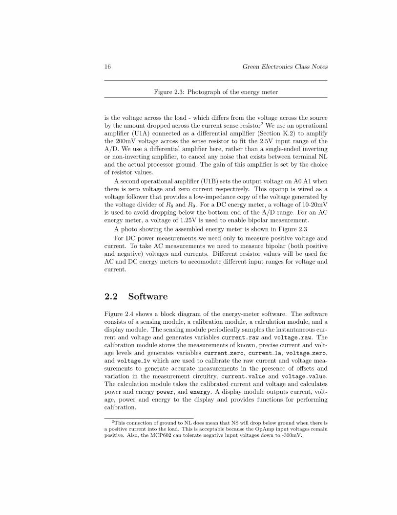
Figure 2.3: Photograph of the energy meter
is the voltage across the load - which differs from the voltage across the sourceby the amount dropped across the current sense resistor2 We use an operationalamplifier (U1A) connected as a differential amplifier (Section K.2) to amplifythe 200mV voltage across the sense resistor to fit the 2.5V input range of theA/D. We use a differential amplifier here, rather than a single-ended invertingor non-inverting amplifier, to cancel any noise that exists between terminal NLand the actual processor ground. The gain of this amplifier is set by the choiceof resistor values.
A second operational amplifier (U1B) sets the output voltage on A0 A1 whenthere is zero voltage and zero current respectively. This opamp is wired as avoltage follower that provides a low-impedance copy of the voltage generated bythe voltage divider of R8 and R9. For a DC energy meter, a voltage of 10-20mVis used to avoid dropping below the bottom end of the A/D range. For an ACenergy meter, a voltage of 1.25V is used to enable bipolar measurement.
A photo showing the assembled energy meter is shown in Figure 2.3For DC power measurements we need only to measure positive voltage and
current. To take AC measurements we need to measure bipolar (both positiveand negative) voltages and currents. Different resistor values will be used forAC and DC energy meters to accomodate different input ranges for voltage andcurrent.
2.2 Software
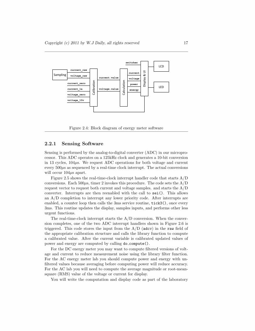
Figure 2.4 shows a block diagram of the energy-meter software. The softwareconsists of a sensing module, a calibration module, a calculation module, and adisplay module. The sensing module periodically samples the instantaneous cur-rent and voltage and generates variables current.raw and voltage.raw. Thecalibration module stores the measurements of known, precise current and volt-age levels and generates variables current zero, current 1a, voltage zero,and voltage 1v which are used to calibrate the raw current and voltage mea-surements to generate accurate measurements in the presence of offsets andvariation in the measurement circuitry, current.value and voltage.value.The calculation module takes the calibrated current and voltage and calculatespower and energy power, and energy. A display module outputs current, volt-age, power and energy to the display and provides functions for performingcalibration.
2This connection of ground to NL does mean that NS will drop below ground when there isa positive current into the load. This is acceptable because the OpAmp input voltages remainpositive. Also, the MCP602 can tolerate negative input voltages down to -300mV.
Copyright (c) 2011 by W.J Dally, all rights reserved 17
Sampling
Cal
ibra
tio
n
current_raw
voltage_raw
Cal
cula
tio
n
current_zero
current_1a
voltage_zero
voltage_10v
current
voltage
power
energy
Dis
pla
y &
UI
current.value
voltage.value
switches
LCD
LED
Figure 2.4: Block diagram of energy meter software
2.2.1 Sensing Software
Sensing is performed by the analog-to-digital converter (ADC) in our micropro-cessor. This ADC operates on a 125kHz clock and generates a 10-bit conversionin 13 cycles, 104µs. We request ADC operations for both voltage and currentevery 500µs as sequenced by a real-time clock interrupt. The actual conversionswill occur 104µs apart.
Figure 2.5 shows the real-time-clock interrupt handler code that starts A/Dconversions. Each 500µs, timer 2 invokes this procedure. The code sets the A/Drequest vector to request both current and voltage samples. and starts the A/Dconverter. Interrupts are then reenabled with the call to sei(). This allowsan A/D completion to interrupt any lower priority code. After interrupts areenabled, a counter loop then calls the 3ms service routine, tick3(), once every3ms. This routine updates the display, samples inputs, and performs other lessurgent functions.
The real-time-clock interrupt starts the A/D conversion. When the conver-sion completes, one of the two ADC interrupt handlers shown in Figure 2.6 istriggered. This code stores the input from the A/D (adcv) in the raw field ofthe appropriate calibration structure and calls the library function to computea calibrated value. After the current variable is calibrated updated values ofpower and energy are computed by calling do compute().
For the DC energy meter you may want to compute filtered versions of volt-age and current to reduce measurement noise using the library filter function.For the AC energy meter lab you should compute power and energy with un-filtered values because averaging before computing power will reduce accuracy.For the AC lab you will need to compute the average magnitude or root-mean-square (RMS) value of the voltage or current for display.
You will write the computation and display code as part of the laboratory

18 Green Electronics Class Notes
rtc()// request conversion on channels 0 and 1adreq |= AD_1 | AD_0 ;if(adidle) start_ad() ;
// reenable interruptssei() ;
// 3ms timerif(++t3 > T3) t3 = 0 ;tick3() ;
Figure 2.5: RTC interrupt handler code
void ad_0() // voltagevoltage.raw = adcv ;calibrate(&voltage) ;
void ad_1() // currentcurrent.raw = adcv ;calibrate(¤t) ;do_compute() ;
Figure 2.6: ADC interrupt handler code

Copyright (c) 2011 by W.J Dally, all rights reserved 19
assignment.
2.3 The Lab
For the laboratory you are to do the following:Part 1: DC energy meter:
1. Calculate the required resistance values to measure 0-60V DC, 0-20A witha 10mΩ sense resistor.
2. Build the energy meter of Figure 2.2 with these values.
3. Using the starter code provided, complete the calculation and display mod-ules to computer power and energy and to display current, voltage, power,and energy on the LCD display. Your code will also need to provide a wayto measure and store the calibration values for your energy meter.
4. Using a lab supply and a lab voltmeter and ammeter, calibrate your energymeter.
5. Using your energy meter, measure the voltage, current, power and energyof (a) a 48V battery driving a heating element, (b) a 48V battery drivingan unloaded electric motor, (c) a 48V battery driving a loaded electricmotor, (d) the load of the setup of (c), and (e) a photovoltaic cell connecteddirectly to a resistive load.
Part 2: AC energy meter:
1. Calculate the required resistance values to measure -200 to 200V, -10 to10A with a 10mΩ sense resistor. Note that a 120V AC line will havevoltages from -170V to 170V over one AC cycle.
2. Build the energy meter of Figure 2.2 with these values.
The AC input will need to be fused but not rectified. To do this with thecomponent module you will need to jumper across the rectifier diode D1.To avoid reverse biasing the electrolytic capacitor, wire POW to COM.Connect nothing else to COM. Wire AC Hot (black wire) from the linecord to the quick-connect lug that feeds the fuse. Connect AC Neutral(white wire) from the line cord to one end of the current sense resistor.Connect your load between the other end of the current sense resistor andPOW. You can monitor the load voltage — with a 100kΩresistor to serveas the upper branch of your voltage divider — via terminal P+.
3. Modify your energy meter code from part 1 to output average AC voltageand current and average power3. Voltage, current, and power compu-tations will need to be integrated over at least one AC cycle to get anaccurate measurement of RMS or average values.
3We leave as an extension computing RMS voltage and current which is what is actuallywanted.
20 Green Electronics Class Notes
4. Using a lab supply and a lab voltmeter and ammeter, calibrate your energymeter.
5. Check out your AC energy meter using a DC lab supply. Reverse thepolarity of the input and verify that current and voltage are negative butthat power and energy are positive. Swap the source and load and verifythat power and energy are negative.
6. (Optional) Using your energy meter, measure the voltage, current, powerand energy of (a) the 110V line driving a resistive load, (b) a 110V linedriving a light bulb, (c) a 110V line driving a fan, and (d) a 110V linedriving a 2.2uF 200V capacitor.
2.4 Extensions
The following are some optional extensions that can be added to the lab:
Timer: Add a feature to the energy meter that allows it to measure energy fora fixed period of time and then stop — holding the final value measured.
RMS Voltage and Current: Add a feature to the AC energy meter to com-pute root-mean-square values for voltage and current measured over thelast 50ms or 1s.
Efficiency Meter: Design an efficiency meter - two energy meters one for inputand one for output and compute the efficiency of the device connectedbetween the two meters. Be careful to account for energy stored in thedevice (in capacitors, inductors, and batteries). You can implement thiswith one processor module by using four of the analog channels.
Temperature Compensation: The resistors we use in the lab have a fairlyhigh temperature coefficient. As a result, your calibration is really onlyvalid at a single temperature. You can compensate for this by measur-ing calibration coefficients at two widely spaced temperatures and thenmeasuring the actual temperature and computing appropriate coefficientsvia interpolation. Using an MCP9701A thermal sensor on analog chan-nel 3 implement a power and energy meter with two-point temperaturecompensation.
Anti-Aliasing: Our input signal conditioning circuit (Figure 2.2) has a flatfrequency response. Thus, noise of all frequencies is input to the A/Dconverter. The sampling process aliases high-frequency noise down intothe band sampled. To reduce noise, and eliminate aliasing, we can im-plement a low-pass filter in each A/D input. With our 1kHz sample ratewe can measure frequencies only up to 500Hz. Higher frequencies willalias into the band from DC to 500Hz. Thus, our low-pass filter shouldattenuate frequencies above this point.

Copyright (c) 2011 by W.J Dally, all rights reserved 21
Design an anti-aliasing filter — i.e., a low-pass filter with a cutoff freuqencyof fc = 500Hz (or lower). This can be accomplished by adding just twocapacitors to Figure 2.2. Implement your filter, and test the resultingenergy meter. Compare its performance to the energy meter withoutfiltering.
Power Factor Measurement: Power factor is the ratio P|V I| averaged over an
AC cycle. For a resistive load, the power factor is 1 while for a reactiveload, a capacitor or inductor, the power factor is zero. Modify your energymeter to measure and display power factor.
Autoranging: Our energy meter has poor relative precision at the low endof its range because the fixed gain is set for the largest possible signal.Fix this issue by modifying the energy meter to automatically vary itscurrent and voltage gain depending on the magnitude of the signal beingmeasured.
For example, for the DC energy meter, the voltage gain can be variedby using a few digital outputs of the microprocessor to pull down on oneof several resistors to form the lower branch of the voltage divider (R2).The outputs connected to the unused resistors are left floating. Gainvariation can aslo be achieved using an external analog multiplexer (becareful about common-mode range) or by using multiple analog inputswith different gain into each.
Better A/D Converter: The 10-bit A/D converter in the AVR microproces-sor is limited. Modify the energy meter to use a higher resolution externalA/D to improve resolution.

22 Green Electronics Class Notes
Chapter 3
Motor Controller
Many green electronic systems use motors to interact with the physical world.For example, an electric or hybrid vehicle uses a motor to propel the vehicle.In other cases motors are used to pump fluids, move air or other gases, controlvalves, etc.... Motors are how all electronic systems affect the physical world.
In all systems that use motors, a motor controller is used to control themotor by regulating the motor voltage and current to achieve a desired angularvelocity ω and/or torque τ . Intelligent control of a motor can often result insignificant energy savings. For example, rather than controlling motor speedby linearly dropping a fixed supply voltage — which dissipates very high powerin the regulator, we use pulse-width modulation to provide the correct averagevoltage to the motor with very low losses in the controller. As a second example,the motor can act as a generator during braking — converting the kinetic energyof the vehicle to electrical energy and returing it to the battery. Many electricand hybrid vehicles use this technique, which is called regenerative braking toimprove their efficiency.
This chapter describes a laboratory where we will build a motor controllerand use this controller to drive a permanent-magnet DC motor at constant speedunder variable load.
In the course of doing this lab you will learn:
Motor Theory: The basics of how voltage v, current i, angular velocity ω,and torque τ are related.
Pulse-Width Modulation: How we can create an effective voltage v by con-trolling the duty-factor of a square-wave signal that switches between twopower supplies.
Buck and Boost Converters: How switching an inductor can (to first ap-proximation) losslessly convert power from a higher voltage to a lowervoltage (a buck converter) and how that same converter running back-wards (a boost converter) converts power from a lower voltage to a highervoltage.
23
24 Green Electronics Class Notes
LM RM
V =KVB
+
-
=K iM
+
-iM
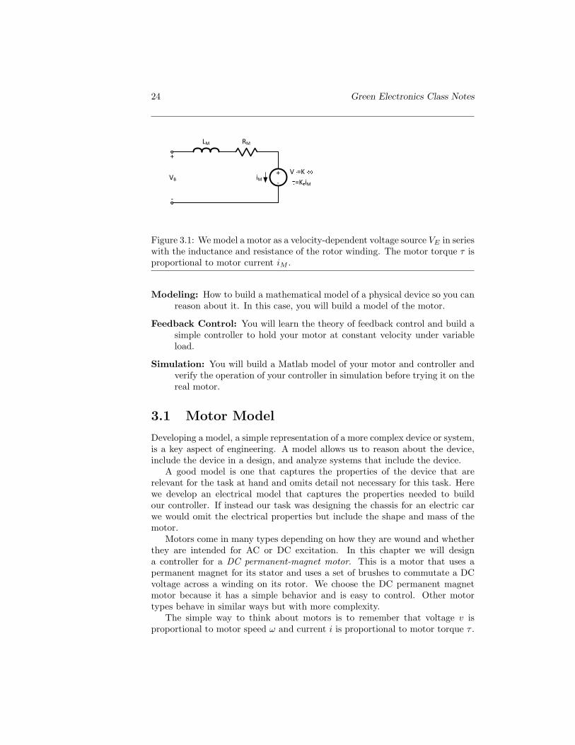
Figure 3.1: We model a motor as a velocity-dependent voltage source VE in serieswith the inductance and resistance of the rotor winding. The motor torque τ isproportional to motor current iM .
Modeling: How to build a mathematical model of a physical device so you canreason about it. In this case, you will build a model of the motor.
Feedback Control: You will learn the theory of feedback control and build asimple controller to hold your motor at constant velocity under variableload.
Simulation: You will build a Matlab model of your motor and controller andverify the operation of your controller in simulation before trying it on thereal motor.
3.1 Motor Model
Developing a model, a simple representation of a more complex device or system,is a key aspect of engineering. A model allows us to reason about the device,include the device in a design, and analyze systems that include the device.
A good model is one that captures the properties of the device that arerelevant for the task at hand and omits detail not necessary for this task. Herewe develop an electrical model that captures the properties needed to buildour controller. If instead our task was designing the chassis for an electric carwe would omit the electrical properties but include the shape and mass of themotor.
Motors come in many types depending on how they are wound and whetherthey are intended for AC or DC excitation. In this chapter we will designa controller for a DC permanent-magnet motor. This is a motor that uses apermanent magnet for its stator and uses a set of brushes to commutate a DCvoltage across a winding on its rotor. We choose the DC permanent magnetmotor because it has a simple behavior and is easy to control. Other motortypes behave in similar ways but with more complexity.
The simple way to think about motors is to remember that voltage v isproportional to motor speed ω and current i is proportional to motor torque τ .
Copyright (c) 2011 by W.J Dally, all rights reserved 25
Hence electrical power (PE = iv) is proportional1 to mechanical power(PM = ωτ).
Figure 3.1 shows the model of a DC permanent-magnet motor we will usein this chapter. The motor is modeled as a voltage source VE that representsthe electromotive force generated by rotating the rotor windings through themagnetic field of the stator. As the motor rotates faster, dφ/dt increases, andthus VE increases.
VE =dφ
dt= KEω. (3.1)
The current through the rotor generates a force with the magnetic field ofthe stator (F = iL×B). This force in turn generates a torque τ on the rotor.
τ = i(L×B)r = Kτ i. (3.2)
The motor dynamics are governed by the angular momentum of the rotatingsystem
ω =1IM
∫τdt, (3.3)
where IM is the moment of inertia of the rotating part of the motor. In thecase where the motor is propelling a mass, such as a vehicle, the mass can beconverted to an addition to the moment of inertia.
Our model includes the parasitic inductance LM and resistance RM of therotor winding.
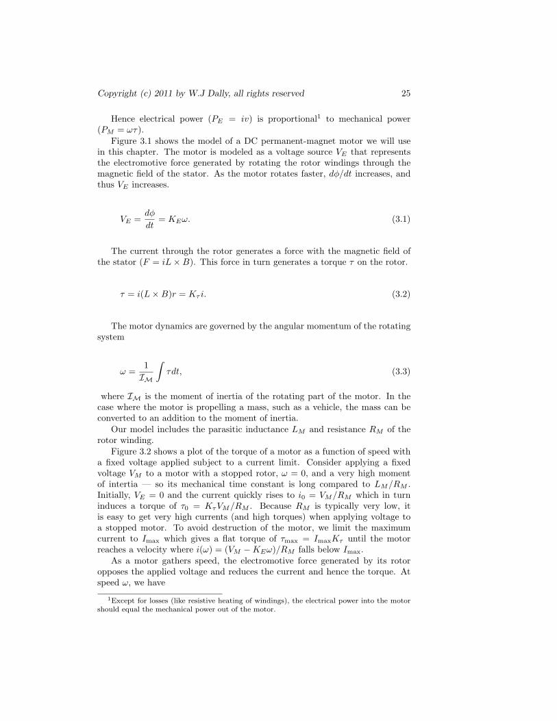
Figure 3.2 shows a plot of the torque of a motor as a function of speed witha fixed voltage applied subject to a current limit. Consider applying a fixedvoltage VM to a motor with a stopped rotor, ω = 0, and a very high momentof intertia — so its mechanical time constant is long compared to LM/RM .Initially, VE = 0 and the current quickly rises to i0 = VM/RM which in turninduces a torque of τ0 = KτVM/RM . Because RM is typically very low, itis easy to get very high currents (and high torques) when applying voltage toa stopped motor. To avoid destruction of the motor, we limit the maximumcurrent to Imax which gives a flat torque of τmax = ImaxKτ until the motorreaches a velocity where i(ω) = (VM −KEω)/RM falls below Imax.
As a motor gathers speed, the electromotive force generated by its rotoropposes the applied voltage and reduces the current and hence the torque. Atspeed ω, we have
1Except for losses (like resistive heating of windings), the electrical power into the motorshould equal the mechanical power out of the motor.
26 Green Electronics Class Notes
Anguar Velocity (rad/s)
Torq
ue
(N
m)
0
max
max
Figure 3.2: Motor torque τ as a function of velocity ω for a constant appliedvoltage subject to a current limit Imax. While current limited τ is constant,then τ falls off linearly with ω.
Copyright (c) 2011 by W.J Dally, all rights reserved 27
48V34AH M
RCSM1
M2
M3
M4
iM
F1
C1
A
A
B
B
S1
S2
C
RL
Optional Load
M5
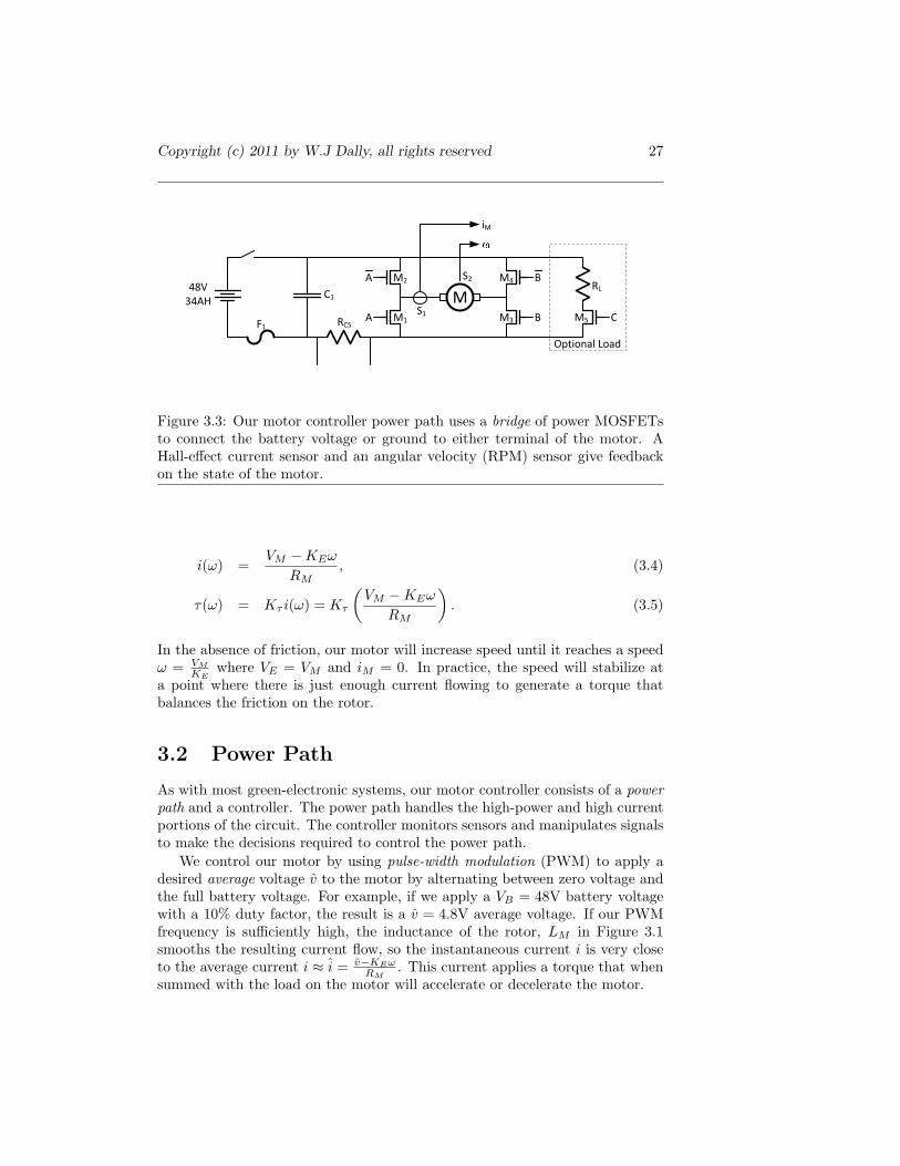
Figure 3.3: Our motor controller power path uses a bridge of power MOSFETsto connect the battery voltage or ground to either terminal of the motor. AHall-effect current sensor and an angular velocity (RPM) sensor give feedbackon the state of the motor.
i(ω) =VM −KEω
RM, (3.4)
τ(ω) = Kτ i(ω) = Kτ
(VM −KEω
RM
). (3.5)
In the absence of friction, our motor will increase speed until it reaches a speedω = VM
KEwhere VE = VM and iM = 0. In practice, the speed will stabilize at
a point where there is just enough current flowing to generate a torque thatbalances the friction on the rotor.
3.2 Power Path
As with most green-electronic systems, our motor controller consists of a powerpath and a controller. The power path handles the high-power and high currentportions of the circuit. The controller monitors sensors and manipulates signalsto make the decisions required to control the power path.
We control our motor by using pulse-width modulation (PWM) to apply adesired average voltage v to the motor by alternating between zero voltage andthe full battery voltage. For example, if we apply a VB = 48V battery voltagewith a 10% duty factor, the result is a v = 4.8V average voltage. If our PWMfrequency is sufficiently high, the inductance of the rotor, LM in Figure 3.1smooths the resulting current flow, so the instantaneous current i is very closeto the average current i ≈ i = v−KEω
RM. This current applies a torque that when
summed with the load on the motor will accelerate or decelerate the motor.
28 Green Electronics Class Notes
The power path that applies pulse-width modulated battery voltage to themotor is shown in Figure 3.3. The circuit uses a bridge of four MOSFETs M1
through M4 to apply either VB or ground to either terminal of the motor. Thetransistors in the bridge operate in pairs so that if M1 is on M2 is off and viceversa. Similarly for M3 and M4. To apply positive voltage across the motor weturn on M2 and M3. Turning on M1 and M4 applies negative voltage acrossthe motor.
If M2 and M4 are turned on, the current in the inductance of the rotorfreewheels around the loop formed. The inductor current freewheels around thelower loop when M1 and M3 are turned on. If either of these cases persists longenough for the current in the motor inductor reverse direction, the motor willbe braked by having its EMF, VE in Figure 3.1 induce a reverse current i thatproduces a torque that opposes the direction of rotation. More on braking inSection 3.3.
If both M3 and M4 are turned off (or if both M1 and M2 are turned off),the motor current will go to zero — after the inductor returns its stored energyto the battery via the body diodes of the MOSFETS. In this state the motorwill coast.
By convention we will use M3 and M4 to control the sign of the appliedaverage voltage v and M1 and M2 to control the magnitude of v. If we onlywant to operate the motor in one direction, we can omit M3 and M4 and tie theright terminal of the motor to ground. Setting B = 1(B = 0) gives a positive vand setting B = 0(B = 1) gives a negative v. With B = 1, the duty factor ofM2, 〈A〉 sets the magnitude of v while the duty factor of M1 〈A〉 = 1−〈A〉 setsthe magnitude when B = 0.
In summary:
v =
(1− 〈A〉)VB if B = 1−〈A〉VB if B = 0.
(3.6)
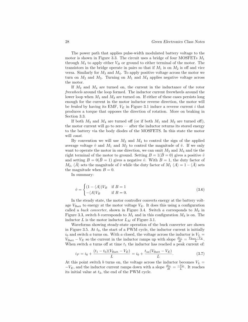
In the steady state, the motor controller converts energy at the battery volt-age VBatt to energy at the motor voltage VE . It does this using a configurationcalled a buck converter, shown in Figure 3.4. Switch a corresponds to M2 inFigure 3.3, switch b corresponds to M1 and in this configuration M3 is on. Theinductor L is the motor inductor LM of Figure 3.1.
Waveforms showing steady-state operation of the buck converter are shownin Figure 3.5. At t0, the start of a PWM cycle, the inductor current is initiallyi0 and switch a turns on. With a closed, the voltage across the inductor is VL =VBatt − VE so the current in the inductor ramps up with slope diL
dt = VBatt−VE
L .When switch a turns off at time t1 the inductor has reached a peak current of:
iP = i0 +(t1 − t0)(VBatt − VE)
L= i0 +
ton(VBatt − VE)L
. (3.7)
At this point switch b turns on, the voltage across the inductor becomes VL =−VE , and the inductor current ramps down with a slope diL
dt = −VE
L . It reachesits initial value at t2, the end of the PWM cycle.
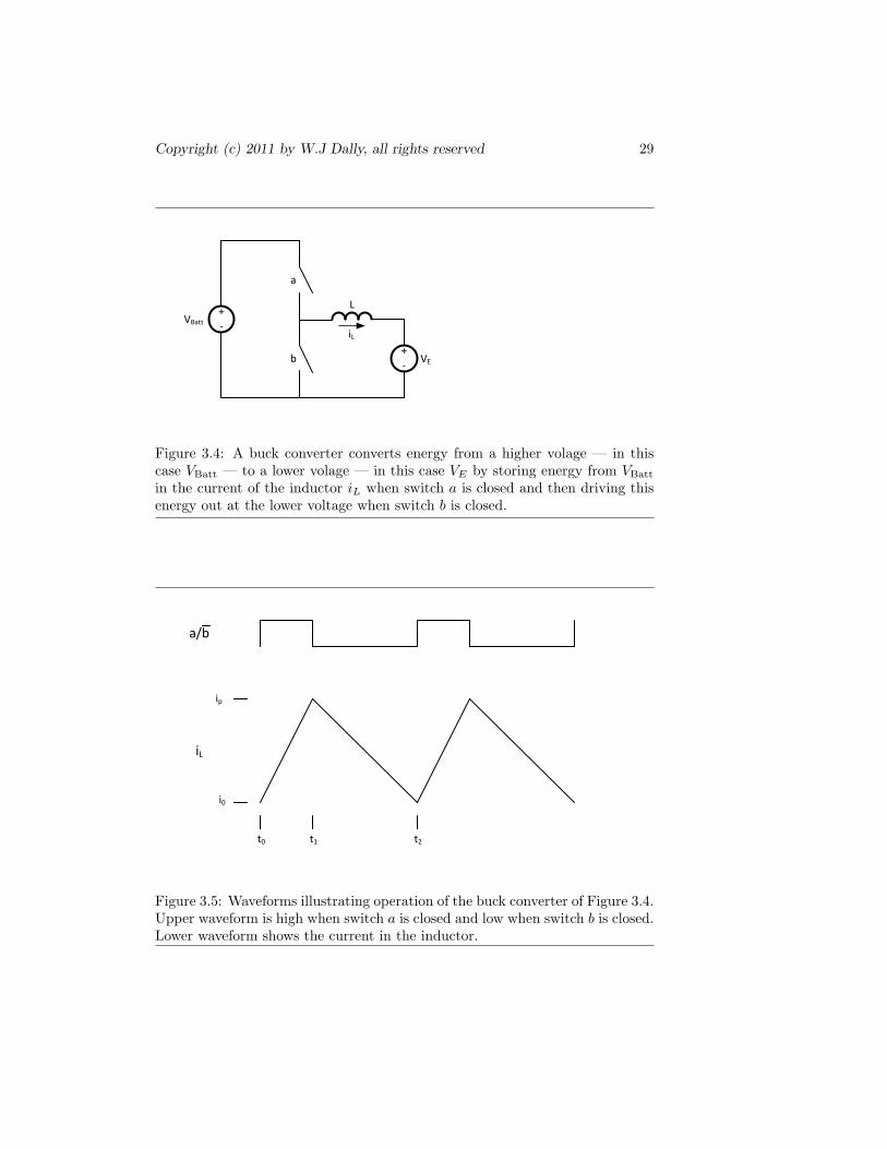
Copyright (c) 2011 by W.J Dally, all rights reserved 29
L
VE
+
-
iL
VBatt
+
-
a
b
Figure 3.4: A buck converter converts energy from a higher volage — in thiscase VBatt — to a lower volage — in this case VE by storing energy from VBatt
in the current of the inductor iL when switch a is closed and then driving thisenergy out at the lower voltage when switch b is closed.
ip
i0
t0 t1 t2
iL
a/b
Figure 3.5: Waveforms illustrating operation of the buck converter of Figure 3.4.Upper waveform is high when switch a is closed and low when switch b is closed.Lower waveform shows the current in the inductor.
30 Green Electronics Class Notes
For steady-state operation the current at the end of the cycle must be thesame as the current at the beginning of the cycle. Thus we have the relationship
toffVE , = ton(VBatt − VE), (3.8)(toff + ton)VE = tcyVE = tonVBatt, (3.9)
VE
VBatt=
tontcy
= 〈A〉. (3.10)
Thus, we see that the buck converter — by storing energy in the magneticfield of an inductor while moving it from one voltage to another — produces anaverage voltage proportional to the duty factor at its output v = 〈A〉VBatt.
The buck converter works equally well regardless of the initial inductor cur-rent i0. In fact, if i0 is negative the converter can work backwards — transferringenergy from the lower-voltage “output” to the higher voltage “input”. Operat-ing in this mode, we call it a boost converter (see Section 3.3). The directionand magnitude of i0, and hence the current and power flow, in a buck converteris determined by the voltages and resistances of the input and output circuits.The buck converter just sets the voltage ratio.
For example, suppose the duty factor is set at 1/3, the input is an idealvoltage source (zero resistance) of VBatt=48V, and the output is voltage sourceof 15V in series with a resistance of 1Ω. In this case, the converter convertsthe 48V to 16V which gives a 1V drop across the load resistance giving a 1Acurrent. If the load source increases to 17V we get 1A flowing in the oppositedirection.
The buck converter is widely used in green electronics, and in power elec-tronics more generally. We will see it again.
As a compromise between minimizing switching losses and minimizing ripplecurrent in the inductor’s windings we choose a PWM frequence of 15kHz.
The power path of Figure 3.3 includes three sensors. A hall effect sensorS1 measures the current into the positive terminal of the motor. This lets usdirectly measure iM and hence τ . An optical sensor S2 generates a pulse trainwith a frequency proportional to the motor speed |ω|. Finally, a sense resistorRCS measures the instantaneous current applied during each pulse.
The input circuit includes a filter capacitor and a fuse. Filter capacitor C1
filters the 15kHz current pulse train to limit the voltage ripple across the bridge.The battery is switched and is fused at its negative terminal. Fusing at thenegative terminal of the battery protects against a short from an intermediateterminal of the battery stack to ground.
The power path includes an optional load resistor RL that is switched byMOSFET M5. This load is used to draw current away from the battery toprevent the battery from overcharging during regenerative braking. By pulse-width modulating signal C controlling M5 with duty factor 〈C〉 the effectiveload resistance becomes Reff = RL/〈C〉.
Copyright (c) 2011 by W.J Dally, all rights reserved 31
L
VE+
-
iL
a
b
VBatt+
-
Figure 3.6: A boost converter converts a low volage — in this case VE — toa higher volage — in this case VBatt by storing energy from VE in the currentof the inductor iL when switch a is closed and then driving this energy out atthe higher voltage when switch b is closed. A boost converter is just a buckconverter with its input and output reversed.
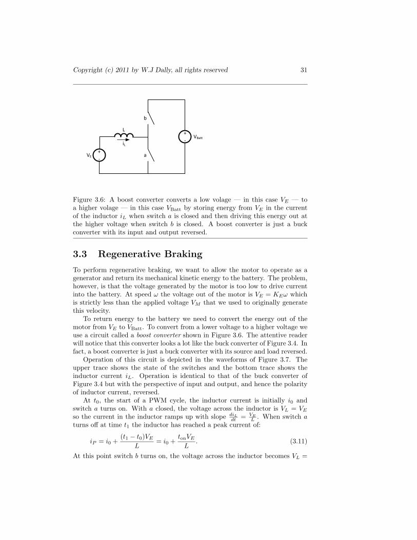
3.3 Regenerative Braking
To perform regenerative braking, we want to allow the motor to operate as agenerator and return its mechanical kinetic energy to the battery. The problem,however, is that the voltage generated by the motor is too low to drive currentinto the battery. At speed ω the voltage out of the motor is VE = KEω whichis strictly less than the applied voltage VM that we used to originally generatethis velocity.
To return energy to the battery we need to convert the energy out of themotor from VE to VBatt. To convert from a lower voltage to a higher voltage weuse a circuit called a boost converter shown in Figure 3.6. The attentive readerwill notice that this converter looks a lot like the buck converter of Figure 3.4. Infact, a boost converter is just a buck converter with its source and load reversed.
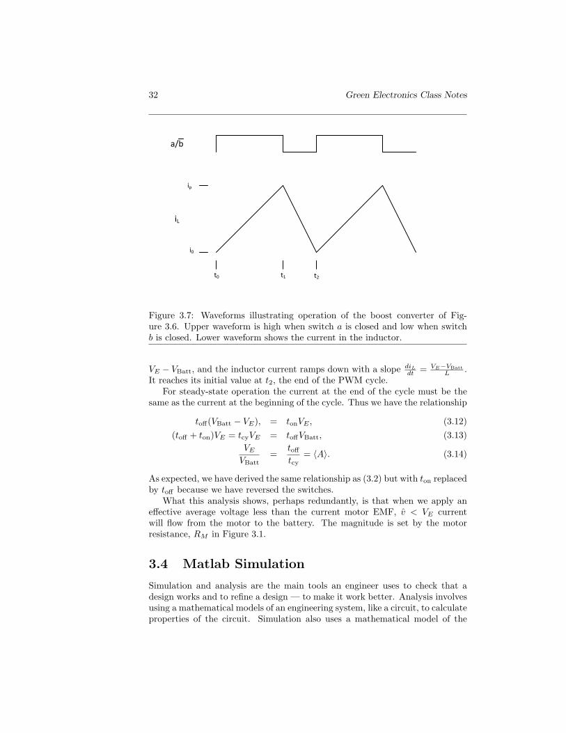
Operation of this circuit is depicted in the waveforms of Figure 3.7. Theupper trace shows the state of the switches and the bottom trace shows theinductor current iL. Operation is identical to that of the buck converter ofFigure 3.4 but with the perspective of input and output, and hence the polarityof inductor current, reversed.
At t0, the start of a PWM cycle, the inductor current is initially i0 andswitch a turns on. With a closed, the voltage across the inductor is VL = VE
so the current in the inductor ramps up with slope diL
dt = VE
L . When switch aturns off at time t1 the inductor has reached a peak current of:
iP = i0 +(t1 − t0)VE
L= i0 +
tonVE
L. (3.11)
At this point switch b turns on, the voltage across the inductor becomes VL =
32 Green Electronics Class Notes
ip
i0
t0 t1 t2
iL
a/b
Figure 3.7: Waveforms illustrating operation of the boost converter of Fig-ure 3.6. Upper waveform is high when switch a is closed and low when switchb is closed. Lower waveform shows the current in the inductor.
VE − VBatt, and the inductor current ramps down with a slope diL
dt = VE−VBattL .
It reaches its initial value at t2, the end of the PWM cycle.For steady-state operation the current at the end of the cycle must be the
same as the current at the beginning of the cycle. Thus we have the relationship
toff(VBatt − VE), = tonVE , (3.12)(toff + ton)VE = tcyVE = toffVBatt, (3.13)
VE
VBatt=
tofftcy
= 〈A〉. (3.14)
As expected, we have derived the same relationship as (3.2) but with ton replacedby toff because we have reversed the switches.
What this analysis shows, perhaps redundantly, is that when we apply aneffective average voltage less than the current motor EMF, v < VE currentwill flow from the motor to the battery. The magnitude is set by the motorresistance, RM in Figure 3.1.
3.4 Matlab Simulation
Simulation and analysis are the main tools an engineer uses to check that adesign works and to refine a design — to make it work better. Analysis involvesusing a mathematical models of an engineering system, like a circuit, to calculateproperties of the circuit. Simulation also uses a mathematical model of the
Copyright (c) 2011 by W.J Dally, all rights reserved 33
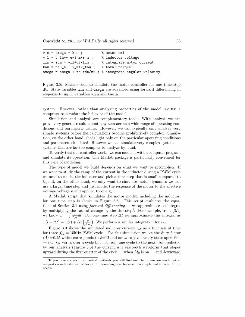
v_e = omega * k_e ; % motor emfv_l = v_in-v_e-i_m*r_m ; % inductor voltagei_m = i_m + v_l*dt/l_m ; % integrate motor currenttau = tau_a + i_m*k_tau ; % total torqueomega = omega + tau*dt/mi ; % integrate angular velocity
Figure 3.8: Matlab code to simulate the motor controller for one time stepdt. State variables i m and omega are advanced using forward differencing inresponse to input variables v in and tau a.
system. However, rather than analyzing properties of the model, we use acomputer to simulate the behavior of the model.
Simulation and analysis are complementary tools. With analysis we canprove very general results about a system across a wide range of operating con-ditions and parametric values. However, we can typically only analyze verysimple systems before the calculations become prohibitively complex. Simula-tion, on the other hand, sheds light only on the particular operating conditionsand parameters simulated. However we can simulate very complex systems —systems that are far too complex to analyze by hand.
To verify that our controller works, we can model it with a computer programand simulate its operation. The Matlab package is particularly convenient forthis type of modeling.
The type of model we build depends on what we want to accomplish. Ifwe want to study the ramp of the current in the inductor during a PWM cyclewe need to model the inductor and pick a time step that is small compared totcy. If, on the other hand, we only want to simulate motor dynamics we canuse a larger time step and just model the response of the motor to the effectiveaverage voltage v and applied torque τa.
A Matlab script that simulates the motor model, including the inductor,for one time step is shown in Figure 3.8. This script evaluates the equa-tions of Section 3.1 using forward differencing — we approximate an integralby multiplying the rate of change by the timestep2. For example, from (3.1)we know ω =
∫τIM dt. For one time step ∆t we approximate this integral as
ω(t + ∆t) = ω(t) + ∆t(
τIM
). We perform a similar integration for iM .
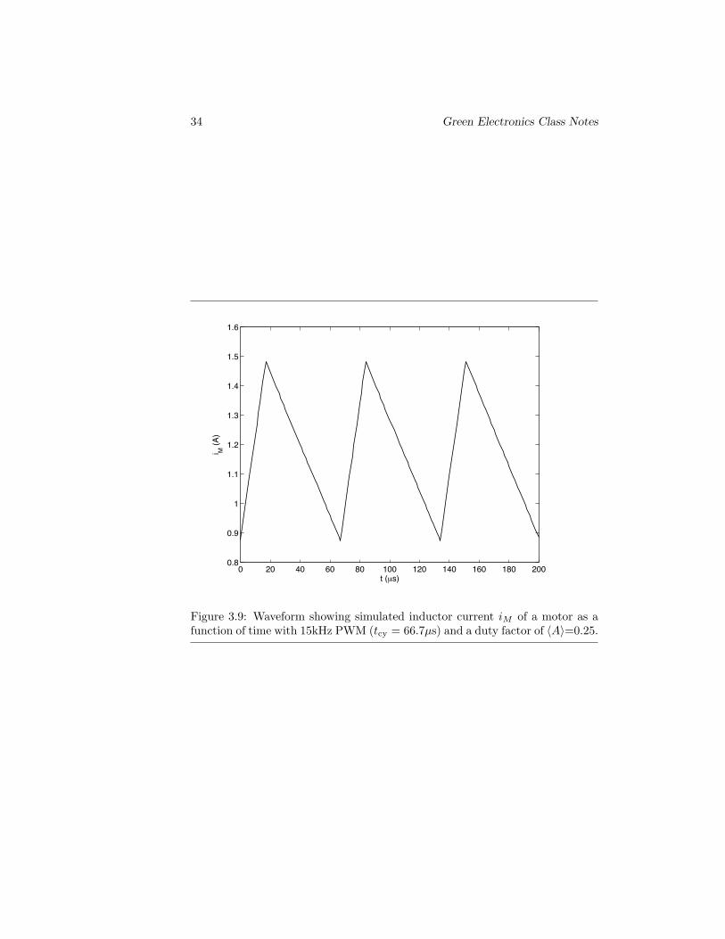
Figure 3.9 shows the simulated inductor current iM as a function of timefor three fcy = 15kHz PWM cycles. For this simulation we set the duty factor〈A〉 =0.25 which corresponds to v=12 and set ω to give steady-state operation— i.e., iM varies over a cycle but not from one-cycle to the next. As predictedby our analysis (Figure 3.5) the current is a sawtooth waveform that slopesupward during the first quarter of the cycle — when M2 is on — and downward
2If you take a class in numerical methods you will find out that there are much betterintegration methods, we use forward differencing here because it is simple and suffices for ourneeds.
34 Green Electronics Class Notes
0 20 40 60 80 100 120 140 160 180 2000.8
0.9
1
1.1
1.2
1.3
1.4
1.5
1.6
i M (A
)
t (µs)
Figure 3.9: Waveform showing simulated inductor current iM of a motor as afunction of time with 15kHz PWM (tcy = 66.7µs) and a duty factor of 〈A〉=0.25.
Copyright (c) 2011 by W.J Dally, all rights reserved 35
0 0.5 1 1.5 2 2.5 30
10
20
30
40
50
60
70
(rad
/s)
t (s)
Figure 3.10: Waveform showing simulated angular velocity ω of a motor as afunction of time with a constant applied voltage VM=10V.
for the last three quarters of the cycle — when M1 is on.
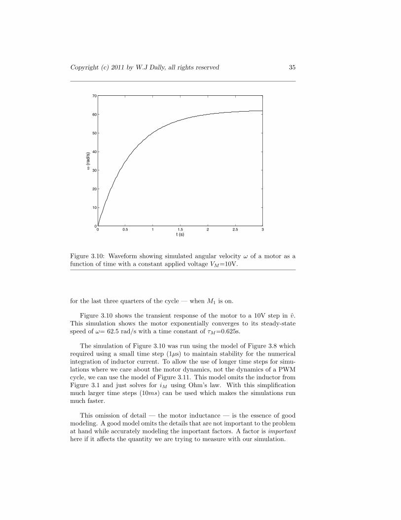
Figure 3.10 shows the transient response of the motor to a 10V step in v.This simulation shows the motor exponentially converges to its steady-statespeed of ω= 62.5 rad/s with a time constant of τM=0.625s.
The simulation of Figure 3.10 was run using the model of Figure 3.8 whichrequired using a small time step (1µs) to maintain stability for the numericalintegration of inductor current. To allow the use of longer time steps for simu-lations where we care about the motor dynamics, not the dynamics of a PWMcycle, we can use the model of Figure 3.11. This model omits the inductor fromFigure 3.1 and just solves for iM using Ohm’s law. With this simplificationmuch larger time steps (10ms) can be used which makes the simulations runmuch faster.
This omission of detail — the motor inductance — is the essence of goodmodeling. A good model omits the details that are not important to the problemat hand while accurately modeling the important factors. A factor is importanthere if it affects the quantity we are trying to measure with our simulation.

36 Green Electronics Class Notes
v_e = omega * k_e ; % motor emfi_m = (v_in-v_e)/r_m ; % motor current - assumes no inductortau = tau_a + i_m*k_tau ;% total torqueomega = omega + tau*dt/mi ; % angular velocity
Figure 3.11: Matlab code to simulate the motor controller for one time step dtignoring the inductor. This permits the use of a larger time step than the modelof Figure 3.8 but cannot be used to study PWM dynamics.
3.5 Controller
When we use a motor in a Green Electronics system we typically want to controlits position, velocity, or torque. To compute the appropriate input v to get thedesired output we use a controller. Most controllers use feedback control asdiscussed in Appendix N.
Consider the problem of building a speed control. The input to our controlleris a desired velocity ωd. The output of our controller is the effective motorvoltage v or equivalently the PWM duty factor 〈A〉. To compute v, a feedbackcontrol system computes an error signal, e(t) = ωd − ω and then computes v asa function of e(t).
A proportional-integral controller (Appendix N) computes the control signalby summing a weighted error signal and a weighted integral of the error signal.
v(t) = pe(t) + q
∫e(t)dt. (3.15)
Here p is the proportional gain and q is the integral gain. Choosing these gainsdetermines the performance and stability of a PI controller.
Our motor has a first-order low-pass response with a time constant τM thatis related to the motor parameters3.
τM =RMIMKτKE
. (3.16)
Thus, we can write the transfer function of the motor as
ω(s) = v(s)(
11 + τs
). (3.17)
Lets pick the frequency4 of our control system as ωc = 2τ . We use the gain
of the control system to give an overall system response that is faster than theplant being controlled.
3 Be careful not to confuse τM the motor time constant with τ its torque — we clearlyneed more greek letters.
4Do not confuse ωc, the natural frequency of the closed-loop system with ω the speed ofthe motor.
Copyright (c) 2011 by W.J Dally, all rights reserved 37
0 0.2 0.4 0.6 0.8 1 1.2 1.4 1.60
20
40
60
(rad
/s)
0 0.2 0.4 0.6 0.8 1 1.2 1.4 1.650
0
50
100
v M (V
)
0 0.2 0.4 0.6 0.8 1 1.2 1.4 1.650
0
50
100
i M (A
)
t (s)
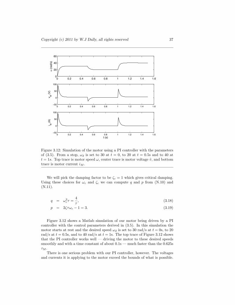
Figure 3.12: Simulation of the motor using a PI controller with the parametersof (3.5). From a stop, ωd is set to 30 at t = 0, to 20 at t = 0.5s and to 40 att = 1s. Top trace is motor speed ω, center trace is motor voltage v, and bottomtrace is motor current iM .
We will pick the damping factor to be ζc = 1 which gives critical damping.Using these choices for ωc and ζc we can compute q and p from (N.10) and(N.11).
q = ω2cτ =
4τ
, (3.18)
p = 2ζτωc − 1 = 3. (3.19)
Figure 3.12 shows a Matlab simulation of our motor being driven by a PIcontroller with the control parameters derived in (3.5). In this simulation themotor starts at rest and the desired speed ωd is set to 30 rad/s at t = 0s, to 20rad/s at t = 0.5s, and to 40 rad/s at t = 1s. The top trace of Figure 3.12 showsthat the PI controller works well — driving the motor to these desired speedssmoothly and with a time constant of about 0.1s — much faster than the 0.625sτM .
There is one serious problem with our PI controller, however. The voltagesand currents it is applying to the motor exceed the bounds of what is possible.
38 Green Electronics Class Notes
0 0.2 0.4 0.6 0.8 1 1.2 1.4 1.60
20
40
60
(rad
/s)
0 0.2 0.4 0.6 0.8 1 1.2 1.4 1.620
0
20
40
v M (V
)
0 0.2 0.4 0.6 0.8 1 1.2 1.4 1.620
0
20
40
i M (A
)
t (s)
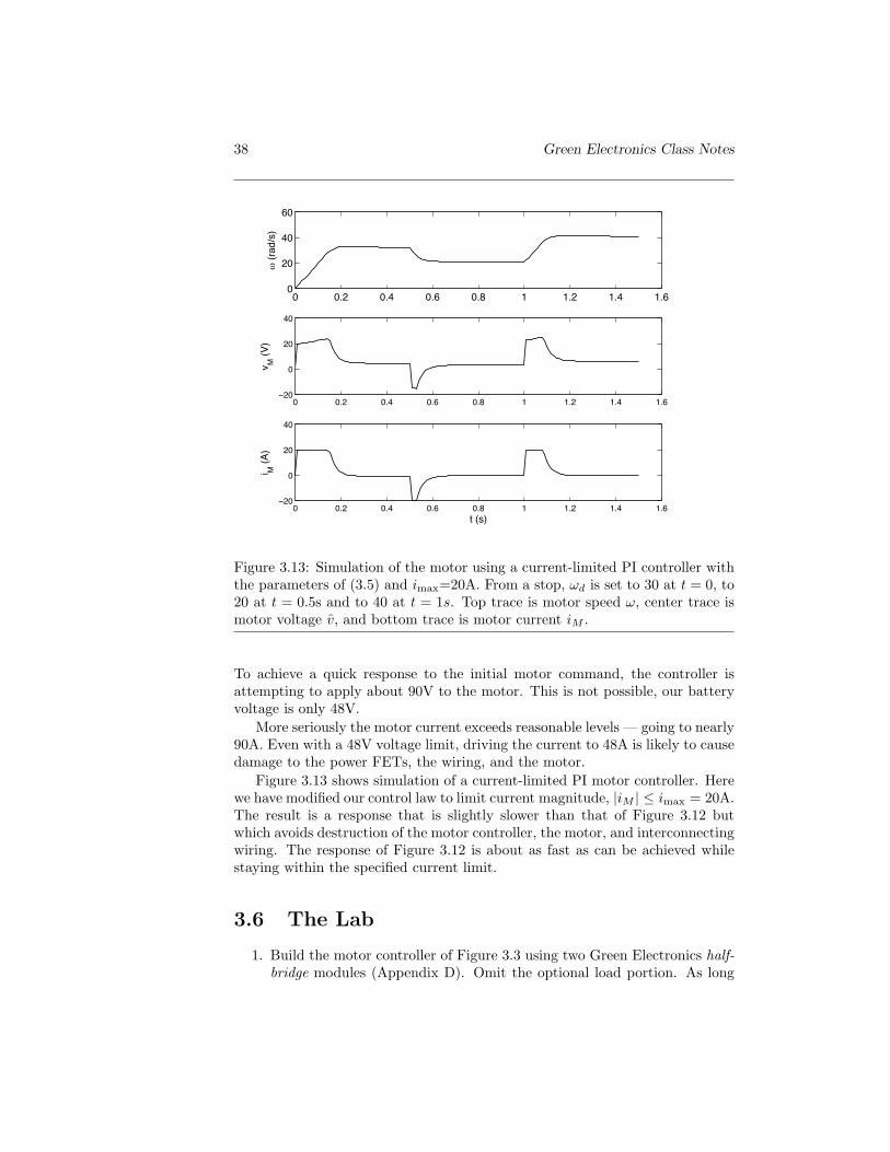
Figure 3.13: Simulation of the motor using a current-limited PI controller withthe parameters of (3.5) and imax=20A. From a stop, ωd is set to 30 at t = 0, to20 at t = 0.5s and to 40 at t = 1s. Top trace is motor speed ω, center trace ismotor voltage v, and bottom trace is motor current iM .
To achieve a quick response to the initial motor command, the controller isattempting to apply about 90V to the motor. This is not possible, our batteryvoltage is only 48V.
More seriously the motor current exceeds reasonable levels — going to nearly90A. Even with a 48V voltage limit, driving the current to 48A is likely to causedamage to the power FETs, the wiring, and the motor.
Figure 3.13 shows simulation of a current-limited PI motor controller. Herewe have modified our control law to limit current magnitude, |iM | ≤ imax = 20A.The result is a response that is slightly slower than that of Figure 3.12 butwhich avoids destruction of the motor controller, the motor, and interconnectingwiring. The response of Figure 3.12 is about as fast as can be achieved whilestaying within the specified current limit.
3.6 The Lab
1. Build the motor controller of Figure 3.3 using two Green Electronics half-bridge modules (Appendix D). Omit the optional load portion. As long
Copyright (c) 2011 by W.J Dally, all rights reserved 39
as the motor is to be run in only one direction the second half-bridge canalso be omitted and the right terminal of the motor can be connected toGND.
2. Develop a motor model. This involves finding the parameters LM , RM ,KE , Kτ , and IM from Figure 3.1, (3.1),(3.1), and (3.1). Write a programfor your motor controller to carry out a series of experiments to measurethese parameters. You have control of voltage v via the PWM duty factorand load and can measure current i and velocity ω. Some experimentsyou might consider include (a) running at a constant voltage at variousloads and measure velocity ω and current i, (b) apply a voltage step andmeasure the transient response of ω and i. Run these experiments andderive your model. Test your model to see how well it predicts observedbehavior.
3. Simulate your motor system in Matlab. Write a Matlab .m file that sim-ulates operation of your motor system. Pick an appropriate timestep ∆tand write code to update the state variables ω, and i each timestep asa function of applied voltage and torque. Run your simulation model onthe test cases you used to develop your model and verify that you get thesame response.
4. Develop a constant-speed controller. Develop a control algorithm andwrite the corresponding control software to maintain your motor at con-stant speed which not exeeding peak current. Test your controller firston your simulation model and then on the actual motor. You controllershould hold speed constant while different loads are applied to the motor— corresponding to a car going up and down hills. It should also tran-sition smoothly between two programmed speeds. The course staff willprogram an adversary load to make it difficult to hold a constant speed.
3.7 Extensions
Regenerative Braking: Add to your controller the ability to perform braking— reducing ω at a specified amount of negative torque τ or eqivalently cur-rent iM . This is needed to slow a car with a controllable force dependingon how hard the driver steps on the brake pedal.
Torque Control: Add to your controller the ability to acclerate with a speci-fied amount of torque τ or equivalently current iM . This is needed to givean acceleration force that is proportional to how far the driver pushes theaccelerator pedal.
Optimize PWM Frequency: We picked the PWM frequency for this lab15kHz somewhat arbitrarily before we measured the motor parameters.

40 Green Electronics Class Notes
Given the motor parameters you measured in your lab, determine an op-timal PWM frequency. You may choose to optimize for efficiency, a fre-quency that gives the lowest losses, performance, a frequency that givesthe fastest response to speed commands (staying within a peak currentlimit).
Program an adversary load: Write the code to drive the “load” generator togive a more sophisticated load for testing motor controllers. Your “load”should simulate the momentum of a car of a specified mass and should beable to model this car going up and down hills of various slope. Note thaton a downhill the load will actually drive the motor and the motor willneed to provide braking — reversing roles with the load.
Vehicle dynamics: Extend your motor simulation model with a model of thedynamics of a vehicle containing the motor. You should take into accountthe mass of the vehicle and account for the momentum of the vehicle andenergy expended and released with the vehicle going up and down hills.
Motor estimation: With accurate motor parameters and a measurement ofmotor current and occasional updates of rotor position your should beable to estimate rotor position at any point in time. Write software toperform this estimation.
Brushless DC Motor Control: A brushless DC motor replaces the mechan-ical commutator of a conventional DC motor with semiconductor switches.Based on the position of the motor multiple windings are switched on andoff and their polarity reversed to provide torque in the desired direction.Write control software to drive the windings of such a motor.
3-Phase AC Motor Control: An AC induction motor requires a three-phasesinusoidal drive where both amplitude and frequency can be controlled.Using three half-bridges build such a motor controller. As a first step,write sofware to generate three-phase sine-waves of specified frequencyand amplitude. As a second step, couple this with a motor estimator andmotor control algorithm to set the frequency, phase, and amplitude toperform constant-speed and constant-torque control with a peak currentconstraint.

Chapter 4
Battery Charger
Energy storage is an important component of many Green Energy systems, andis often provided by batteries. In this chapter we will develop a model of a bat-tery and will then use our model do drive design of a battery charger. Differentbatteries have different properties, different models, and different charging re-quirements. In this chapter we restrict our attention to deep-cycle lead/acidbatteries such as are found in golf carts and some other electric vehicles.
This chapter describes a laboratory where you will build a battery chargerto charge a 48V lead-acid battery pack from 110V 60Hz AC wall current. Inthe course of this laboratory you will learn
Battery Characteristics: The basics of how batteries work as viewed fromtheir terminals, in particular their V-I characteristics and charging char-acteristics.
Modeling: You will practice the modeling skills you developed in Chapter 3by developing a model for our battery pack.
AC Rectification: How AC current is converted to DC current using a diode.
Buck Converter: Some details of the buck converter, introduced in Section 3.2,as it is applied to efficiently convert a high voltage to a lower voltage.
Layered Control: How to decompose a complex control task into several sim-ple layers.
Current-Mode Control: A method for controlling a pulse-width-modulatedsystem, like the buck converter, by controlling the current in the inductoreach cycle.
4.1 Modeling a Battery
Just as we developed a motor model in Section 3.1 we will develop a batterymodel that captures just the behavior of the battery that we need to know to
41
42 Green Electronics Class Notes
LB RB
VBS VB
+
-
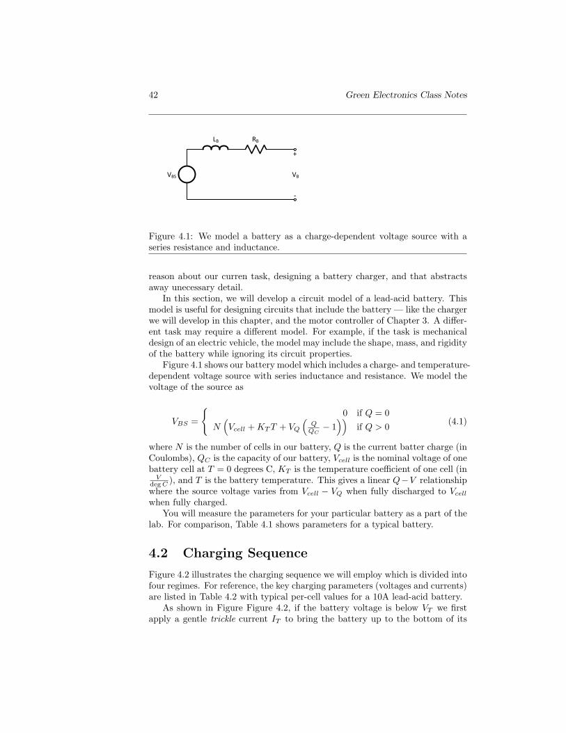
Figure 4.1: We model a battery as a charge-dependent voltage source with aseries resistance and inductance.
reason about our curren task, designing a battery charger, and that abstractsaway unecessary detail.
In this section, we will develop a circuit model of a lead-acid battery. Thismodel is useful for designing circuits that include the battery — like the chargerwe will develop in this chapter, and the motor controller of Chapter 3. A differ-ent task may require a different model. For example, if the task is mechanicaldesign of an electric vehicle, the model may include the shape, mass, and rigidityof the battery while ignoring its circuit properties.
Figure 4.1 shows our battery model which includes a charge- and temperature-dependent voltage source with series inductance and resistance. We model thevoltage of the source as
VBS =
0 if Q = 0
N(Vcell + KT T + VQ
(Q
QC− 1))
if Q > 0 (4.1)
where N is the number of cells in our battery, Q is the current batter charge (inCoulombs), QC is the capacity of our battery, Vcell is the nominal voltage of onebattery cell at T = 0 degrees C, KT is the temperature coefficient of one cell (in
Vdeg C ), and T is the battery temperature. This gives a linear Q−V relationshipwhere the source voltage varies from Vcell − VQ when fully discharged to Vcell
when fully charged.You will measure the parameters for your particular battery as a part of the
lab. For comparison, Table 4.1 shows parameters for a typical battery.
4.2 Charging Sequence
Figure 4.2 illustrates the charging sequence we will employ which is divided intofour regimes. For reference, the key charging parameters (voltages and currents)are listed in Table 4.2 with typical per-cell values for a 10A lead-acid battery.
As shown in Figure Figure 4.2, if the battery voltage is below VT we firstapply a gentle trickle current IT to bring the battery up to the bottom of its
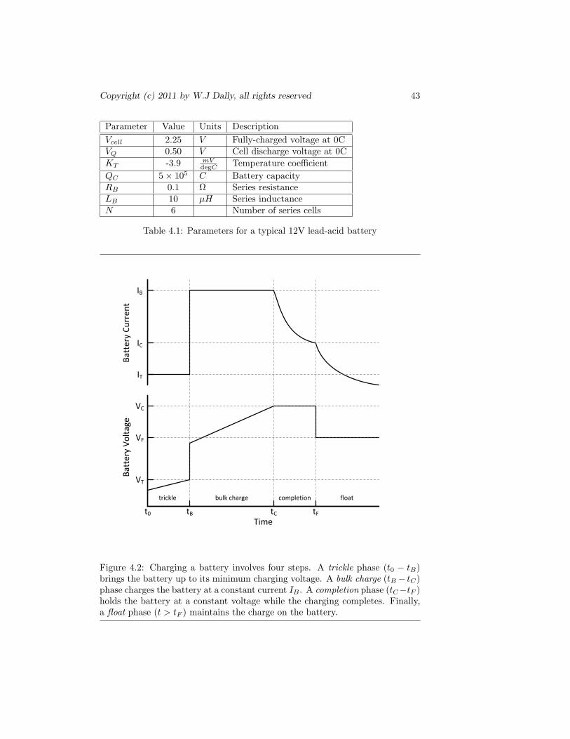
Copyright (c) 2011 by W.J Dally, all rights reserved 43
Parameter Value Units DescriptionVcell 2.25 V Fully-charged voltage at 0CVQ 0.50 V Cell discharge voltage at 0CKT -3.9 mV
degC Temperature coefficientQC 5× 10⁵ C Battery capacityRB 0.1 Ω Series resistanceLB 10 µH Series inductanceN 6 Number of series cells
Table 4.1: Parameters for a typical 12V lead-acid battery
IB
IT
IC
VT
VC
VF
t0 tB tC tF
Bat
tery
Vo
ltag
eB
atte
ry C
urr
ent
Time
trickle bulk charge completion float
Figure 4.2: Charging a battery involves four steps. A trickle phase (t0 − tB)brings the battery up to its minimum charging voltage. A bulk charge (tB − tC)phase charges the battery at a constant current IB . A completion phase (tC−tF )holds the battery at a constant voltage while the charging completes. Finally,a float phase (t > tF ) maintains the charge on the battery.
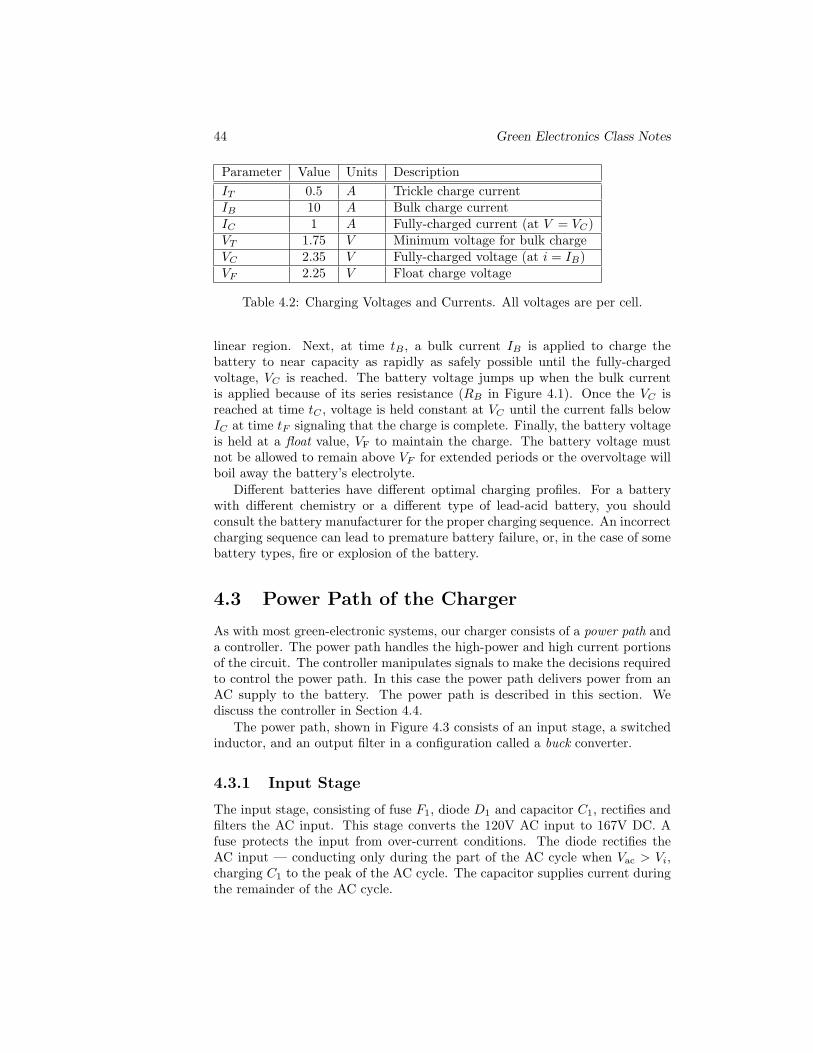
44 Green Electronics Class Notes
Parameter Value Units DescriptionIT 0.5 A Trickle charge currentIB 10 A Bulk charge currentIC 1 A Fully-charged current (at V = VC)VT 1.75 V Minimum voltage for bulk chargeVC 2.35 V Fully-charged voltage (at i = IB)VF 2.25 V Float charge voltage
Table 4.2: Charging Voltages and Currents. All voltages are per cell.
linear region. Next, at time tB , a bulk current IB is applied to charge thebattery to near capacity as rapidly as safely possible until the fully-chargedvoltage, VC is reached. The battery voltage jumps up when the bulk currentis applied because of its series resistance (RB in Figure 4.1). Once the VC isreached at time tC , voltage is held constant at VC until the current falls belowIC at time tF signaling that the charge is complete. Finally, the battery voltageis held at a float value, VF to maintain the charge. The battery voltage mustnot be allowed to remain above VF for extended periods or the overvoltage willboil away the battery’s electrolyte.
Different batteries have different optimal charging profiles. For a batterywith different chemistry or a different type of lead-acid battery, you shouldconsult the battery manufacturer for the proper charging sequence. An incorrectcharging sequence can lead to premature battery failure, or, in the case of somebattery types, fire or explosion of the battery.
4.3 Power Path of the Charger
As with most green-electronic systems, our charger consists of a power path anda controller. The power path handles the high-power and high current portionsof the circuit. The controller manipulates signals to make the decisions requiredto control the power path. In this case the power path delivers power from anAC supply to the battery. The power path is described in this section. Wediscuss the controller in Section 4.4.
The power path, shown in Figure 4.3 consists of an input stage, a switchedinductor, and an output filter in a configuration called a buck converter.
4.3.1 Input Stage
The input stage, consisting of fuse F1, diode D1 and capacitor C1, rectifies andfilters the AC input. This stage converts the 120V AC input to 167V DC. Afuse protects the input from over-current conditions. The diode rectifies theAC input — conducting only during the part of the AC cycle when Vac > Vi,charging C1 to the peak of the AC cycle. The capacitor supplies current duringthe remainder of the AC cycle.
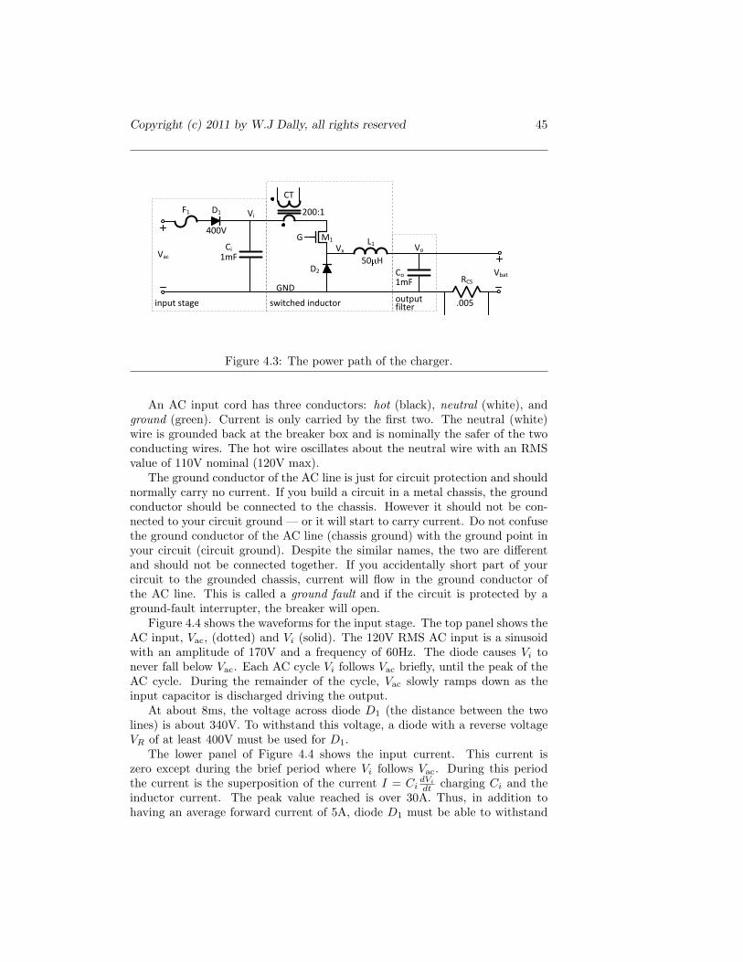
Copyright (c) 2011 by W.J Dally, all rights reserved 45
Vac
RCS
Vbat
L1
CoD2
D1
G M1
Ci
CT
200:1
50 H
.005
1mF
1mF
Vx
F1
400V
Vi
GND
Vo
input stage switched inductor output filter
Figure 4.3: The power path of the charger.
An AC input cord has three conductors: hot (black), neutral (white), andground (green). Current is only carried by the first two. The neutral (white)wire is grounded back at the breaker box and is nominally the safer of the twoconducting wires. The hot wire oscillates about the neutral wire with an RMSvalue of 110V nominal (120V max).
The ground conductor of the AC line is just for circuit protection and shouldnormally carry no current. If you build a circuit in a metal chassis, the groundconductor should be connected to the chassis. However it should not be con-nected to your circuit ground — or it will start to carry current. Do not confusethe ground conductor of the AC line (chassis ground) with the ground point inyour circuit (circuit ground). Despite the similar names, the two are differentand should not be connected together. If you accidentally short part of yourcircuit to the grounded chassis, current will flow in the ground conductor ofthe AC line. This is called a ground fault and if the circuit is protected by aground-fault interrupter, the breaker will open.
Figure 4.4 shows the waveforms for the input stage. The top panel shows theAC input, Vac, (dotted) and Vi (solid). The 120V RMS AC input is a sinusoidwith an amplitude of 170V and a frequency of 60Hz. The diode causes Vi tonever fall below Vac. Each AC cycle Vi follows Vac briefly, until the peak of theAC cycle. During the remainder of the cycle, Vac slowly ramps down as theinput capacitor is discharged driving the output.
At about 8ms, the voltage across diode D1 (the distance between the twolines) is about 340V. To withstand this voltage, a diode with a reverse voltageVR of at least 400V must be used for D1.
The lower panel of Figure 4.4 shows the input current. This current iszero except during the brief period where Vi follows Vac. During this periodthe current is the superposition of the current I = Ci
dVi
dt charging Ci and theinductor current. The peak value reached is over 30A. Thus, in addition tohaving an average forward current of 5A, diode D1 must be able to withstand
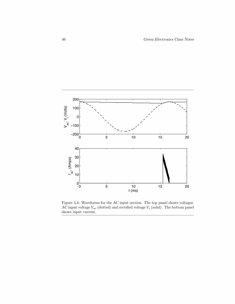
46 Green Electronics Class Notes
0 5 10 15 20200
100
0
100
200
V ac, V
i (Vol
ts)
0 5 10 15 200
10
20
30
40
I ac, (
Amps
)
t (ms)
Figure 4.4: Waveforms for the AC input section. The top panel shows voltages:AC input voltage Vac (dotted) and rectified voltage Vi (solid). The bottom panelshows input current.
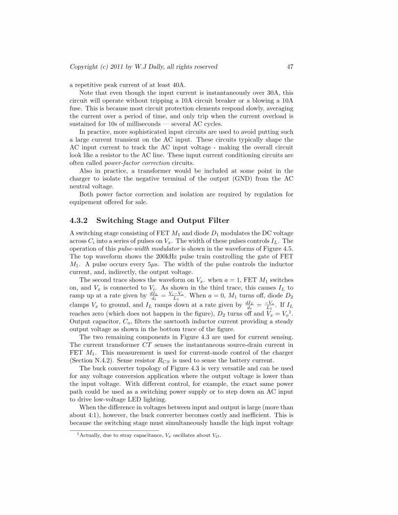
Copyright (c) 2011 by W.J Dally, all rights reserved 47
a repetitive peak current of at least 40A.Note that even though the input current is instantaneously over 30A, this
circuit will operate without tripping a 10A circuit breaker or a blowing a 10Afuse. This is because most circuit protection elements respond slowly, averagingthe current over a period of time, and only trip when the current overload issustained for 10s of milliseconds — several AC cycles.
In practice, more sophisticated input circuits are used to avoid putting sucha large current transient on the AC input. These circuits typically shape theAC input current to track the AC input voltage - making the overall circuitlook like a resistor to the AC line. These input current conditioning circuits areoften called power-factor correction circuits.
Also in practice, a transformer would be included at some point in thecharger to isolate the negative terminal of the output (GND) from the ACneutral voltage.
Both power factor correction and isolation are required by regulation forequipement offered for sale.
4.3.2 Switching Stage and Output Filter
A switching stage consisting of FET M1 and diode D1 modulates the DC voltageacross Ci into a series of pulses on Vx. The width of these pulses controls IL. Theoperation of this pulse-width modulator is shown in the waveforms of Figure 4.5.The top waveform shows the 200kHz pulse train controlling the gate of FETM1. A pulse occurs every 5µs. The width of the pulse controls the inductorcurrent, and, indirectly, the output voltage.
The second trace shows the waveform on Vx. when a = 1, FET M1 switcheson, and Vx is connected to Vi. As shown in the third trace, this causes IL toramp up at a rate given by dIL
dt= Vi−Vo
L1. When a = 0, M1 turns off, diode D2
clamps Vx to ground, and IL ramps down at a rate given by dIL
dt= −Vo
L1. If IL
reaches zero (which does not happen in the figure), D2 turns off and Vx = Vo1.
Output capacitor, Co, filters the sawtooth inductor current providing a steadyoutput voltage as shown in the bottom trace of the figure.
The two remaining components in Figure 4.3 are used for current sensing.The current transformer CT senses the instantaneous source-drain current inFET M1. This measurement is used for current-mode control of the charger(Section N.4.2). Sense resistor RCS is used to sense the battery current.
The buck converter topology of Figure 4.3 is very versatile and can be usedfor any voltage conversion application where the output voltage is lower thanthe input voltage. With different control, for example, the exact same powerpath could be used as a switching power supply or to step down an AC inputto drive low-voltage LED lighting.
When the difference in voltages between input and output is large (more thanabout 4:1), however, the buck converter becomes costly and inefficient. This isbecause the switching stage must simultaneously handle the high input voltage
1Actually, due to stray capacitance, Vx oscillates about VO.
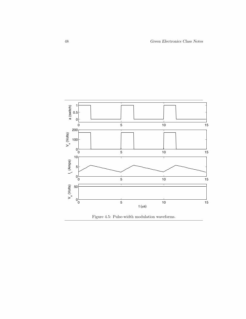
48 Green Electronics Class Notes
0 5 10 150
0.5
1
a (s
witc
h)
0 5 10 150
100
200
V x (Vol
ts)
0 5 10 150
5
10
I L (Am
ps)
0 5 10 150
50
V o (Vol
ts)
t (µs)
Figure 4.5: Pulse-width modulation waveforms.
Copyright (c) 2011 by W.J Dally, all rights reserved 49
State Machine
V or IControl
State
Vbat
Ibat
PWMCurrentControl
Imax
IM1 G
Figure 4.6: Layered controller for the battery charger
and the high output current. When a large step-down (or step-up) is required,a full-bridge or half-bridge converter, using a transformer is more efficient.
The actual buck converter is a bit more complicated than what we haveshown here. It includes a high-side driver to provide the voltage levels neededto drive the gate G of M1, a power supply for this high-side driver including astart-up supply, and a snubber on the drain of M1 to avoid high voltage-spikesdue to the inductance of the current transformer when M1 switches off. Fordetails of these circuits see Appendix E.
4.4 Control of the Charger
4.4.1 Layered Control
The battery charger uses a layered controller, illustrated in Figure 4.6. Layeredcontrol is a common theme in green electronics systems. Each level of thecontroller monitors its inputs, performs a control function, and sends a commandto the next lower layer. Layered control partitions a complex controller ina manner that each individual layer and box is fairly simple. Thus, both theindividual modules and the controller as a whole are easily understood, designed,and modified.
Our controller has three layers. The top layer is a state machine that deter-ines — by monitoring battery voltage and current — which of the four chargingphases of Figure 4.2 the controller is in. The middle layer is a voltage or cur-rent regulator. Depending on the state, it either holds current constant (in

50 Green Electronics Class Notes
Off Trick Bulk Comp Float
Off I = IT I = IB V = VC V = VF
VT>V≥0 V≥VT
VB>V≥VT
V≥VC
VMax>V≥VC
Reset, V<0,
V>VMax I<IF
Figure 4.7: State diagram of the battery charger.
the trickle and bulk charge phases), or voltage constant (in the completion andfloat phases). This layer holds the appropriate variable constant by setting Imax,the maximum inductor current. The bottom layer, in this case the PWM con-troller, controls the power path, in this case by driving G, the gate of FET M1
in Figure 4.3. It monitors the current in FET M1 (via the current transformer)and terminates each PWM pulse when the desired maximum current, Imax, isreached.
4.4.2 State Machine
Figure 4.7 shows the state diagram of the top level of the controller of Figure 4.6.The system has five states, Off, Trick, Comp, Top, and Float the last four ofwhich correspond to the four phases of charging shown in Figure 4.2. Transitionsbetween the states are made when various voltage and current thresholds arereached. The label below each state indicates the function of the controllerin that state. The controller regulates current in states Trick and Bulk andregulates voltage in states Comp and Float.
The system starts in the Off state with no current flowing. The system willstay in the Off state, and will return to this state from any other state, if reversepolarity is sensed or if the battery voltage exceeds a maximum value VMax.
The transition out of the Off state depends on the battery voltage. If thebattery voltage is below threshold VT , the controller enters the Trick (tricklecharge) state to trickle charge the battery at a relatively low current IT untilit reaches threashold. If the battery starts above threshold — or after it hasbeen trickle charged to this state — the controller enters the Bulk state to bulkcharge the battery by holding the current at the bulk charge level IB . If thebattery is at a voltage at or above the completion voltage VC , the charger entersthe Comp state. The charger transitions from each state to its right neighborwhen the appropriate voltage or current threshold is reached.
Copyright (c) 2011 by W.J Dally, all rights reserved 51
4.4.3 Buck Regulator
The second level of the controller of Figure 4.6 is a current-mode buck controller(Section N.4.2) that regulates the battery voltage or current depending on thecurrent state. The quantity regulated is depicted under each state in Figure 4.7.For example, in the bulk state current is regulated so that I = IB and duringthe comp state, voltage is regulated so that V = VC .
The current mode controller commands the target inductor current Imax asneeded to achieve the regulation goal. As described in Section N.4.2, we use asimple PI controller to compute Imax from an error term e.
Imax = pe + q
∫edt (4.2)
Following the derivation in Sections N.2 and N.4.2, we choose ω = 62.8(10Hz) to allow software to close the loop with a 1kHz sample rate and a 100Hzcommand bandwidth, and we choose ζ = 1 to provide critical damping. Fromthese two choices, we use Equation (N.45) to derive q = 3.95 and (N.46) toderive p = 0.125.
These values of p and q are used when we are controlling voltage. Whenwe are controlling current, we must compensate for the gain represented by theseries resistance of the battery, RB . A differential change in battery voltage∆v produces a differential change in batter current ∆i = ∆v
RB. Thus, from the
point of view of the controller, the battery is a stage with gain 1RB
that convertsvoltage to current. To compensate, we multiply our controller gains by RB
when regulating current. Assuming the value RB = 0.1Ω from Table 4.1 wehave qi = qRB = 0.395 and pi = pRB = 0.0125.
To check our choice of p and q, we use Matlab to compute the open-loopfrequency response of our controller (Figure 4.8). The figure shows a unity-gainfrequency of 20.6Hz and a phase margin of 76.
A controller with a unity-gain frequency of 20Hz may seem slow. However,this is plenty fast to charge a battery. Choosing a low ω allows us to implementthe middle level of our controller in software and to use a relatively slow PWMoutput on our microprocessor to generate the voltage that controls Imax.
4.4.4 PWM Current-Mode Control
The bottom layer of our controller controls the pulse-width applied to MOSFETM1 in Figure 4.3 to maintain the desired maximum inductor current Imax. Thislayer of the controller uses a UC3843 current-mode PWM controller integratedcircuit connected as shown in Figure 4.9. The UC3843 combines an oscillator, anop-amp, a comparator, a flip-flop, an output driver, an undervoltage protectioncircuit, and a flip-flop.
The PWM waveform is generated to regulate current by setting the flip-flop with the oscillator and resetting it with the comparator. The oscillatorgenerates a sawtooth waveform with a frequency given by f = 1.64
R5C3. Once each
cycle, the flip-flop is set, causing a rising edge on the PWM output which turns
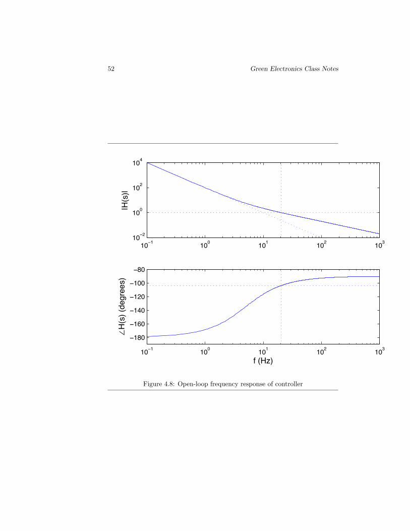
52 Green Electronics Class Notes
10 1 100 101 102 10310 2
100
102
104
|H(s
)|
10 1 100 101 102 103
180
160
140
120
100
80
H(s
) (de
gree
s)
f (Hz)
Figure 4.8: Open-loop frequency response of controller
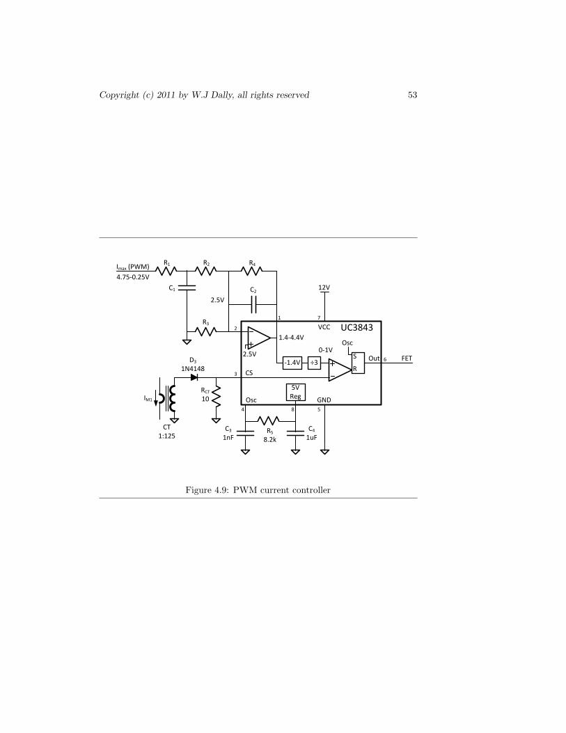
Copyright (c) 2011 by W.J Dally, all rights reserved 53
2
1
R2 R4
C2
RCT
10
D3
1N4148
CT1:125
3
12V
7
6
R5
8.2k
C3
1nFC4
1uF
4 8 5
FET
IM1
UC3843VCC
GND
Out
Osc
CS
S
R-1.4V ÷3
Imax (PWM)
0-1V
1.4-4.4V
4.75-0.25V
2.5V
R3
Osc
2.5V
5V Reg
R1
C1
Figure 4.9: PWM current controller

54 Green Electronics Class Notes
on FET M1. As current builds in inductor L1, the current transformer sensesthis current and resistor RCT generates a current-sense voltage. When thiscurrent sense voltage (on pin 3 of the UC3843) exceeds the value at the positiveterminal of the internal comparator (which reflects Imax) the flip-flop resets,causing a falling edge on the PWM output and limiting the inductor current tothe specified Imax.
Current Sense
To provide a maximum inductor current of 10A, the current sense circuit needsto provide a 1V signal at pin 3 of the UC3843 when the inductor current reachesabout 10A. The current transformer has a turns ratio of 1:125. Thus, a 10Ainductor current is reduced to a 80mA current in the secondary. A 10Ω resistorprovides a signal that reaches 1V at an inductor current of 12.5A.
The diode in series with the resistor rectifies the current — providing theproper offset. Because the transformer only couples the AC component of theMOSFET current, the signal out of the current transformer is offset — goingbelow ground when the actual MOSFET current is zero. The diode cancels thisoffset.
Low-pass Filter
The Imax signal is generated as a pulse-width modulated digital signal from oneof the microcontroller’s timer/counters. We use the op-amp (pins 1 and 2) ofthe UC3843 as a low-pass filter and level translator to convert this pulse trainto a level signal on pin 1 of the UC3843. Resistors R1 to R4 and capacitors C1
and C2 configure the op-amp for this functionality2.The DC response of this circuit is set by the four resistors to translate an
input range of 4.75-0.25V to an output range of 1.4-4.4V. (For arcane reasons,internal block of hte UC3843 apply the function f(x) = x−1.4
3 to the voltageon the output of the op-amp before applying it to the positive input of thecomparator, so the 1.4-4.4V range is ultimately converted to a 0-1V range atthe comparator.) We leave it as an exercise for you to calculate the values forR1 to R4 and C1 to C2. Note that for R1 and C1 to be an effective low-passstage, R1 must be at least an order of magnitude smaller than R2.
To smooth the PWM Imax pulse train into a DC level, we use a two-polelow-pass filter. The first pole is provided by R1 and C1 and the second poleis provided by R4 and C2. The cutoff frequencies f = 1
2πRC for these twofilter stages should be chosen small enough so that the AC component of thePWM signal is attenuated by at least 40dB (100×), but high enough to give aquick response to changes in this signal — quick compared to the speed of themiddle-level control loop which has a bandwidth of 10Hz.
2The UC3843 provides this op-amp to implment the PI controller (the middle-level of ourlayered control) we implement the PI controller in the microcontroller and choose to use theop-amp as a level translator and filter.

Copyright (c) 2011 by W.J Dally, all rights reserved 55
4.5 Simulation
In this section we simulate our battery charger using Matlab. Like any model, asimulation model is tailored to the questions that need to be answered. In thissection we are concerned with the overall behavior of our charger — what thegeneral shape of the waveforms are and how our control law operates. We choosenot to model the details of the switching transient — which would be requiredto calculate switching losses for example. As with any engineering model, theprinciple here is to keep things as simple as possible, but no simpler. Nothingis gained by adding unnecessary complexity to a model, and a lot of time iswasted.
We start our simulation model by writing a Matlab function bcupdate.m(Figure 4.10) that advances the state of our power path by one timestep. Thestate of our power path is to first order described by the state variables of theenergy storage devices: the voltage across the input capacitor Vi, the voltageacross the output capacitor Vo, and the current through the inductor, IL. Wemodel these three state variables as Matlab variables v i, v o, and i l respec-tively. The code in Figure 4.10 computes difference variables dv i, dv o, anddi l which reflect how much each of the state variables changes in one timestep, dt. For example, if the switch is closed ((a==1)), we compute dv i =-i l*dt/c i. This is directly from the constituent equation of the capacitori = C dv
dt . Which can be rewritten as dv = idtC .
After the difference variables are computed using the old values of the statevariables, we update the state variables by adding the difference variables, e,g.,v i = v i + dv i.
The last portion of the code in Figure 4.10 simulates the input stage. Thiscode updates v i to follow the AC input if v ac > v i and calculates the result-ing input capacitor current. When the switch is closed, v i has already beendecremented to account for the inductor current, so the value computed for i acincludes the inductor current.
Figure 4.11 shows the Matlab code to simulate our battery charger powerpath for one PWM cycle tc. The first part of the code simulates the battery,computing the battery voltage (v bat) and current (i bat), and updating thecharge state (q).
The bottom portion of the code loops over the timesteps within a PWMcycle (steps) calling bcupdate for each timestep. The switch starts out closedat the beginning of each PWM cycle (a = 1). Then, each step we check if theinductor current has reached the set value (i l >= i a) and if so, open theswitch. Once the switch is set to the appropriate state, bcupdate is called tosimulate one timestep. The final line of the loop logs per-timestep values to beused in plots.
What remains is to simulate the upper two layers of our three-layer controlsystem. The code for this is shown in Figure 4.12. This code also runs onceeach PWM cycle. The case statement simulates the state machine, advancing tothe next state when the specified conditions are met. The PI controller is thensimulated by computing the error (err) integrating it to compute the integral

56 Green Electronics Class Notes
% bcupdate.m update vi, vo, il for one timestep
% simulate switching stageif (a==1) % switch closeddv_i = -i_l*dt/c_i ; % input capacitordi_l = (v_i-v_o)*dt/l ; % inductor
else % switch opendv_i = 0 ; % input capacitordi_l = -v_o*dt/l ; % inductor
enddv_o = (i_l-(v_o-v_bat)/r_b)*dt/c_o ; % output capacitor
% update v_i, v_o, and i_l by adding deltasv_i = v_i + dv_i ; % this gets i_l incorporated automaticallyv_o = v_o + dv_o ;i_l = max(0, i_l + di_l) ; % diode keeps i_l non negative
% simulate input rectifierv_ac = v_acmax*cos(t*omega) ;if (v_ac > v_i) % rectifier diode is ondv_i = v_ac - v_i ;v_i = v_ac ;i_ac = dv_i*c_i/dt ;
else % rectifier diode is offi_ac = 0 ;
end
Figure 4.10: Matlab simulation model to advance the state of the battery chargerpower path by one timestep, dt.
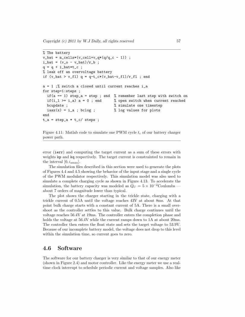
Copyright (c) 2011 by W.J Dally, all rights reserved 57
% The batteryv_bat = n_cells*(v_cell+v_q*(q/q_c - 1)) ;i_bat = (v_o - v_bat)/r_b ;q = q + i_bat*t_c ;% leak off an overvoltage batteryif (v_bat > v_fl) q = q-t_c*(v_bat-v_fl)/r_fl ; end
a = 1 ;% switch a closed until current reaches i_afor step=1:steps ;if(a == 1) step_a = step ; end % remember last step with switch onif(i_l >= i_a) a = 0 ; end % open switch when current reachedbcupdate ; % simulate one timestepiaax(x) = i_a ; bclog ; % log values for plots
endt_a = step_a * t_c/ steps ;
Figure 4.11: Matlab code to simulate one PWM cycle tc of our battery chargerpower path.
error (ierr) and computing the target current as a sum of these errors withweights kp and kq respectively. The target current is constrainted to remain inthe interval [0, iamax].
The simulation files described in this section were used to generate the plotsof Figures 4.4 and 4.5 showing the behavior of the input stage and a single cycleof the PWM modulator respectively. This simulation model was also used tosimulate a complete charging cycle as shown in Figure 4.13. To accelerate thesimulation, the battery capacity was modeled as QC = 5 × 10⁻²Coulombs —about 7 orders of magnitude lower than typical.
The plot shows the charger starting in the trickle state, charging with atrickle current of 0.5A until the voltage reaches 43V at about 8ms. At thatpoint bulk charge starts with a constant current of 5A. There is a small over-shoot as the controller settles to this value. Bulk charge continues until thevoltage reaches 56.4V at 19ms. The controller enters the completion phase andholds the voltage at 56.4V while the current ramps down to 1A at about 20ms.The controller then enters the float state and sets the target voltage to 53.9V.Because of our incomplete battery model, the voltage does not drop to this levelwithin the simulation time, so current goes to zero.
4.6 Software
The software for our battery charger is very similar to that of our energy meter(shown in Figure 2.4) and motor controller. Like the energy meter we use a real-time clock interrupt to schedule periodic current and voltage samples. Also like

58 Green Electronics Class Notes
% the state machineswitch statecase ’trick’ % trickmode = ’current’ ;i_t = i_trick ;if(v_o > v_trick) state = ’bulk’ ; end
case ’bulk’ % bulkmode = ’current’ ;i_t = i_bulk ;if(v_o > v_c) state = ’top’ ; end
case ’top’ % topmode = ’voltage’ ;v_t = v_c ;if(i_bat < i_c) state = ’float’ ; end
case ’float’ % floatmode = ’voltage’ ;v_t = v_float ;
end
% control lawif(mode == ’voltage’) err = v_t - v_o ;else err = (i_t - i_bat)*r_b ;endierr = ierr + err*t_c ; % integrate
i_a = max(0, min(i_amax, kp*err + kq*ierr)) ;
Figure 4.12: Matlab code to simulate one PWM cycle tc of the control law.

Copyright (c) 2011 by W.J Dally, all rights reserved 59
0 5 10 15 20 2540
50
60
V o (V)
0 5 10 15 20 2540
50
60
V bat (V
)
0 5 10 15 20 250
5
10
I bat (A
)
t (ms)
Figure 4.13: Result of simulating an entire charging cycle: trickle, bulk, com-pletion, and float. The battery capacity QC has been artificially reduced byseveral orders of magnitude to accelerate the simulation.
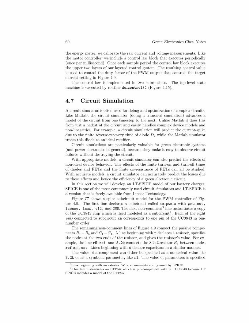
60 Green Electronics Class Notes
the energy meter, we calibrate the raw current and voltage measurements. Likethe motor controller, we include a control law block that executes periodically(once per millisecond). Once each sample period the control law block executesthe upper two layers of our layered control system. The resulting control valueis used to control the duty factor of the PWM output that controls the targetcurrent setting in Figure 4.9.
The control law is implemented in two subroutines. The top-level statemachine is executed by routine do control() (Figure 4.15).
4.7 Circuit Simulation
A circuit simulator is often used for debug and optimization of complex circuits.Like Matlab, the circuit simulator (doing a transient simulation) advances amodel of the circuit from one timestep to the next. Unlike Matlab it does thisfrom just a netlist of the circuit and easily handles complex device models andnon-linearities. For example, a circuit simulation will predict the current-spikedue to the finite reverse-recovery time of diode D2 while the Matlab simulatortreats this diode as an ideal rectifier.
Circuit simulations are particularly valuable for green electronic systems(and power electronics in general), because they make it easy to observe circuitfailures without destroying the circuit.
With appropriate models, a circuit simulator can also predict the effects ofnon-ideal device behavior. The effects of the finite turn-on and turn-off timesof diodes and FETs and the finite on-resistance of FETs can all be studied.With accurate models, a circuit simulator can accurately predict the losses dueto these effects and hence the efficiency of a green electronic circuit.
In this section we will develop an LT-SPICE model of our battery charger.SPICE is one of the most commmonly used circuit simulators and LT-SPICE isa version that is freely available from Linear Technology.
Figure ?? shows a spice subcircuit model for the PWM controller of Fig-ure 4.9. The first line declares a subcircuit called cm pwm a with pins out,isense, imax, v12, and GND. The next non-comment3 line instantiates a copyof the UC3843 chip which is itself modeled as a subcircuit4. Each of the eightpins connected to subcircuit xa corresponds to one pin of the UC3843 in pin-number order.
The remaining non-comment lines of Figure 4.9 connect the passive compo-nents R1−R5 and C1−C4. A line beginning with r declares a resistor, specifiesthe nodes at the two ends of the resistor, and gives the resistor’s value. For ex-ample, the line r5 ref osc 8.2k connects the 8.2kΩresistor R5 between nodesref and osc. Lines beginning with c declare capacitors in a similar manner.
The value of a component can either be specified as a numerical value like8.2k or as a symbolic parameter, like r1. The value of parameters is specified
3lines beginning with an asterisk “*” are comments and ignored by SPICE.4This line instantiates an LT1247 which is pin-compatible with teh UC3843 because LT
SPICE includes a model of the LT1247.

Copyright (c) 2011 by W.J Dally, all rights reserved 61
// the control algorithm - runs at 1kHzvoid do_control() // FSMif((voltage <= 0)||(voltage > vmax)) state = S_OFF ;switch(state) case S_OFF: // off initially or if voltage out of rangeif((voltage > 0) && (voltage < vmax)) init_pi() ; state = S_TRICK ;OCR1B = 0xFFF ;break ;
case S_TRICK: // trickle charge until at VTif(voltage > vt) init_pi() ; state = S_BULK ;do_pi_control(SET_I, it) ;break ;
case S_BULK: // bulk charge until VOCif(voltage > voc) tcount++ ;if(tcount >= S_COUNT) tcount = 0 ; init_pi() ; state = S_TOP ;
else tcount = 0 ;do_pi_control(SET_I, ib) ;break ;
case S_TOP: // hold voltage at VOC until IOCif(current < ioc) tcount++ ;if(tcount >= S_COUNT) tcount = 0 ; init_pi() ; state = S_FLOAT ;
else tcount = 0 ;if(current > (ib+IFUZZ)) bcount++ ;if(bcount >= S_COUNT) bcount = 0 ; init_pi() ; state = S_BULK ;
else bcount = 0 ;do_pi_control(SET_V, voc) ;break ;
case S_FLOAT: // then floatif(current > ioc+IFUZZ) bcount++ ;if(bcount >= S_COUNT) bcount = 0 ; init_pi() ; state = S_BULK ;
else bcount = 0 ;do_pi_control(SET_V, vfloat) ;break ;
default:state = S_OFF ;break ;
Figure 4.14: “C” code that implements the charging state machine. This codeexecutes at 1kHz (once per millisecond).

62 Green Electronics Class Notes
// do_pi_control - one time step of PI controllervoid do_pi_control(int mode, int16_t target) int16_t value ;
// select current or voltage modeif(mode == SET_I) value = current ; p = pi ; q = qi ; // current modeelse value = voltage ; p = pv ; q = qv ; // voltage mode
// compute errorserr = target - value ;ierr = ierr + err ; // scaled by 1/dt (factor into Q)if(ierr > IERR_MAX) ierr = IERR_MAX ;if(ierr < -IERR_MAX) ierr = -IERR_MAX ;
// the control lawcontrol = p*err + q*ierr ;
// scalingcontrol = control>>SHIFT ; // to normalize - 1 = 11bits.control = 3000L - control ; // offset to middle of range and invertif(control > 4095L) control = 4095L ; // saturateif(control < 0L) control = 0L ;OCR1B = control ;
Figure 4.15: “C” code that implements the PI controller. This code executes at1kHz (once per millisecond).
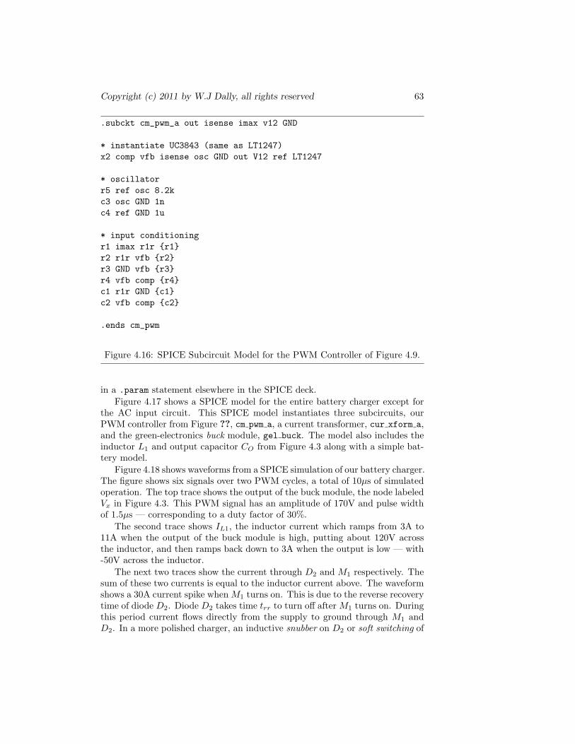
Copyright (c) 2011 by W.J Dally, all rights reserved 63
.subckt cm_pwm_a out isense imax v12 GND
* instantiate UC3843 (same as LT1247)x2 comp vfb isense osc GND out V12 ref LT1247
* oscillatorr5 ref osc 8.2kc3 osc GND 1nc4 ref GND 1u
* input conditioningr1 imax r1r r1r2 r1r vfb r2r3 GND vfb r3r4 vfb comp r4c1 r1r GND c1c2 vfb comp c2
.ends cm_pwm
Figure 4.16: SPICE Subcircuit Model for the PWM Controller of Figure 4.9.
in a .param statement elsewhere in the SPICE deck.Figure 4.17 shows a SPICE model for the entire battery charger except for
the AC input circuit. This SPICE model instantiates three subcircuits, ourPWM controller from Figure ??, cm pwm a, a current transformer, cur xform a,and the green-electronics buck module, gel buck. The model also includes theinductor L1 and output capacitor CO from Figure 4.3 along with a simple bat-tery model.
Figure 4.18 shows waveforms from a SPICE simulation of our battery charger.The figure shows six signals over two PWM cycles, a total of 10µs of simulatedoperation. The top trace shows the output of the buck module, the node labeledVx in Figure 4.3. This PWM signal has an amplitude of 170V and pulse widthof 1.5µs — corresponding to a duty factor of 30%.
The second trace shows IL1, the inductor current which ramps from 3A to11A when the output of the buck module is high, putting about 120V acrossthe inductor, and then ramps back down to 3A when the output is low — with-50V across the inductor.
The next two traces show the current through D2 and M1 respectively. Thesum of these two currents is equal to the inductor current above. The waveformshows a 30A current spike when M1 turns on. This is due to the reverse recoverytime of diode D2. Diode D2 takes time trr to turn off after M1 turns on. Duringthis period current flows directly from the supply to ground through M1 andD2. In a more polished charger, an inductive snubber on D2 or soft switching of

64 Green Electronics Class Notes
* instantiate the UC3843 and componentsxpwm pwm isense imax V12 GND cm_pwm_a
* current sensexct vd vdd isense GND cur_xform_a
* buck modulexbuck vdd out pwm GND V12 gel_buck
* InductorL1 out ld 22uH
* output capacitorCO ld GND 1000uF
* battery modelVL bat GND 48RL ld bat 0.1
* suppliesVD vd GND 170V12 V12 GND 12VVin imax GND 2.6
.ic v(pwm:comp)=2.8
.tran tcy*ncy
Figure 4.17: SPICE Model for the battery charger.
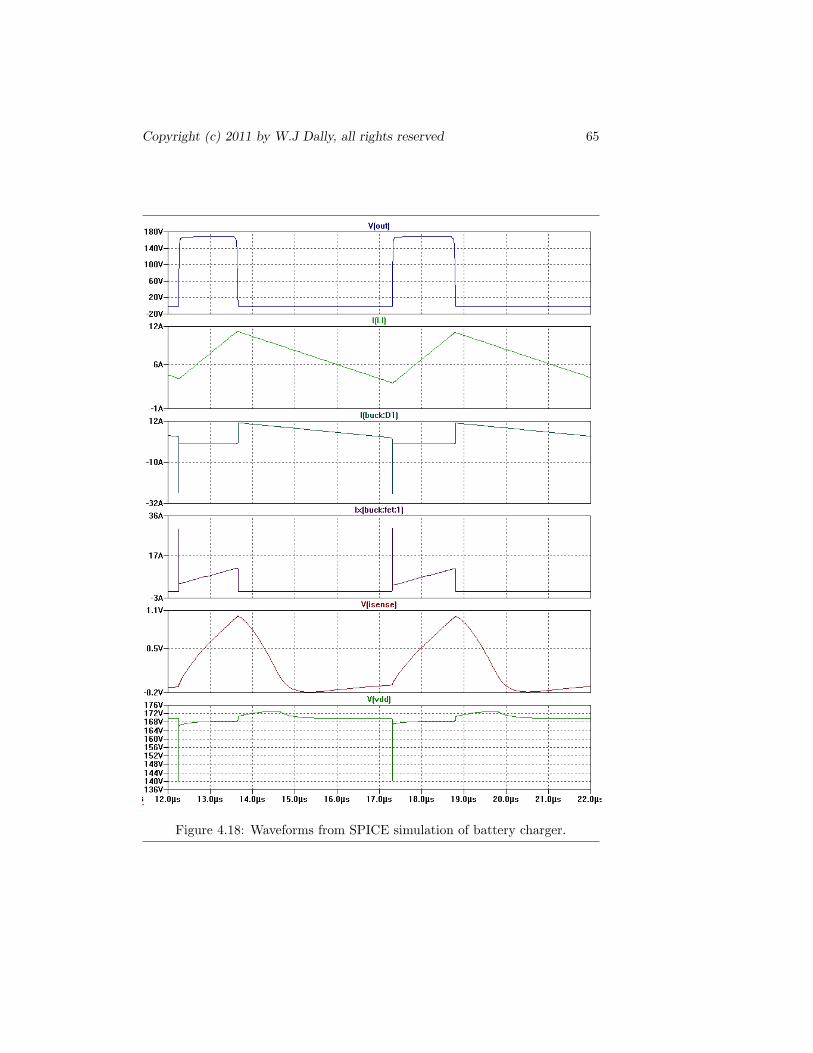
Copyright (c) 2011 by W.J Dally, all rights reserved 65
Figure 4.18: Waveforms from SPICE simulation of battery charger.
66 Green Electronics Class Notes
M1 would be employed to avoid this shoot-through current.
Ignoring the shoot-through current for the moment, these two waveformsshow that M1 carries the inductor current during the upward ramp and D2
carries the current during the downward ramp as expected.
The fifth waveform is the voltage across the current sense resistor on thesecondary of the current transformer. This signal shows that the transformercurrent ramps up with the current in M1 but then continues after M1 turnsoff. This is due to the inductance of the current transformer. A capacitivesnubber on the drain of M1 in the buck module prevents the energy stored inthis inductor from causing a damaging voltage spike on the drain of M1 duringturn-off.
The bottom trace of Figure 4.18 shows the voltage on the drain of M1. Thisvoltage drops briefly to 140V as M1 turns on as the shoot-through current isdropped across the resistor of the drain snubber in the buck module. It thensettles just slightly below the 170V input voltage as the current in M1 rampsup. It goes a few volts above the input voltate when M1 turns off as the energystored in the inductance of the current transformer is absorbed by the drainsnubber.
SPICE simulation is particularly useful for studying switching losses. Fig-ure 4.19 shows the current through, voltage across, and power dissipated inMOSFET M1 during the turn-on transient. As the figure shows, the shoot-through current that occurs before diode D2 recovers causes the current toramp to 30A while the voltage across the device is over 140 V. The result is aninstantaneous power of over 4kW for a few nanoseconds. The current settlesdown to 4 A while the voltage ramps from 130V down to zero. This results inthe power ramping from about 400W down to zero over about 25ns. The energydissipated during the turn-on switching event, the area under the power curve,is measured (using a SPICE .meas statement) to be 13.1µJ.
The turn-off transient is shown in Figure 4.20. Here the current holds steadyat 11A while the voltage ramps up to 170V over 25ns resulting in the powerramping up to 1.7kW. The energy dissipated during the turn-off event is mea-sured to be 31.2µJ. Even though there is no shoot-through current, the turn-offloss is substantially larger than the turn-on loss because the inducotr currentat turn-off is almost four times larger than the current at turn-on. The totalswitching energy is 44.3µJ each 200kHz cycle giving a switching power of 8.86W.The 0.9W conduction loss due to the FET’s 30mΩRon is small in comparison.
Of course these predictions of switching loss, like any SPICE results, areonly as good as the models used in the SPICE simulation. This simulation usesMOSFET and diode models provided by the manufacturers but ignores almostall layout parasitics — the stray inductance and capacitance due to wires andprinted-circuit board traces. In practice these parasitic circuit elements canbe quite important and may cause actual circuit behavior to deviate from thesimulation results in significant ways. For truly accurate simulation results thesecircuit elements need to be accurately modeled.
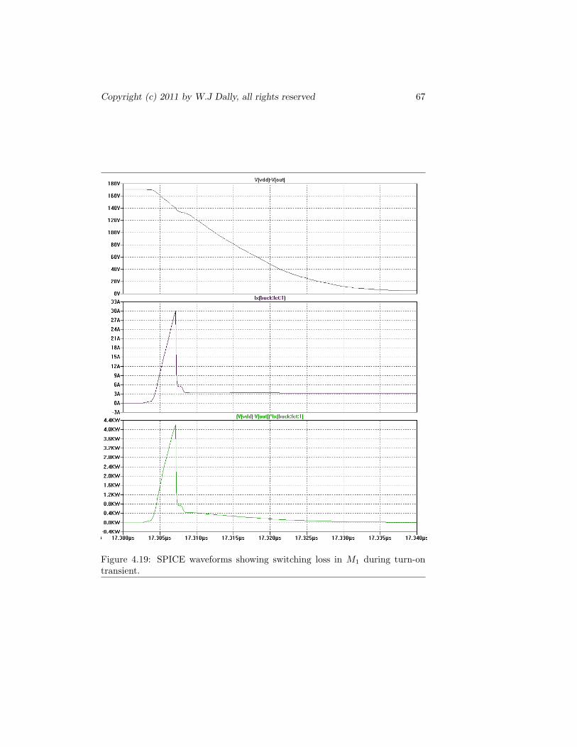
Copyright (c) 2011 by W.J Dally, all rights reserved 67
Figure 4.19: SPICE waveforms showing switching loss in M1 during turn-ontransient.

68 Green Electronics Class Notes
Figure 4.20: SPICE waveforms showing switching loss in M1 during turn-offtransient.

Copyright (c) 2011 by W.J Dally, all rights reserved 69
4.8 The Lab
For the laboratory you should do the following:
1. Using a lab power supply and power resistor to source and sink currentfrom the battery, estimate the series resistance of the battery, RB in Fig-ure 4.1.
2. Calculate appropriate values for R1 to R4, C1, and C2 and, using thesevalues, build the PWM controller illustrated in Figure 4.9.
3. Run a SPICE simulation of your charger using the resistor values youcalculated.
4. Build and incrementally verify your PWM controller. Start by checkingthat the oscillator (pin 4) has a 200kHz sawtooth waveform. Next, applya PWM waveform to the left side of R1 and verify that the OpAmp outputhas a smooth DC voltage that can be varied from 1.4 to 4.4 V as the PWMduty factor is varied.
5. Assemble the power path of your charger (Figure 4.3). Use a lab powersupply to supply voltage to your charger, and a resistive load in place ofthe battery during verification to limit damage if something goes wrong.
6. With the lab supply connected across the input capacitor verify the oper-ation of your charger. Verify one layer of your controller at a time. Startby putting your charger in a mode where you can manually set the PWMduty factor and verify that the controller behaves as expected. Next, putthe charger in a mode where you can manually specify the current or volt-age the charger is to produce and verify that the charger regulates to thisvalue. Finally put the charger into its normal operating mode and verifythat it sequenes through the charging states.
Limit your charging current to no more than 4A to avoid overheating theinductor on the component board.
7. Repeat your verification with your charger connected to the battery —but still powered from the lab supply. You can determine the batteryinductance LB at this time.
8. Finally, connect your charger to the AC line and verify that it operates asexpected.
4.9 Extensions
More Accurate Battery Model: Our battery model is too simple to capturemany important electrical characteristics of a lead-acid battery. Determinethe shortcomings of our model and develop a more accurate model thatovercomes these shortcomings.

70 Green Electronics Class Notes
Slope Compensation: Regulating maximum PWM current — as performedby our UC3843 can result in unstable operation when the duty factorexceeds 50%. At high duty factors the controller can alternate between afat pulse and a skinny pulse. A technique called slope compensation canelminate this unstable behavior. Implement slope compensation in thislab.
Synchronous Rectification: Losses can be reduced by replacing the diode D2
in the power path with a second MOSFET. Implement a battery chargerusing this techqnique, which is called synchronous rectification.
Soft Switching: Our battery charger has high switching losses because MOS-FET M1 turns on with high voltage (170V) across it and turns off withhigh current (up to 10A). The turn-on transient is particularly costly be-cause diode D2 does not turn off instantly. During the reverse-recoverytime of D2 M1 shorts 170V to ground and can draw a very large amountof current until the diode stops conducting.
Redesign the converter to use soft switching so that the MOSFET onlyswitches when it has either zero voltage across its terminals (ZVS) or zerocurrent flowing through it (ZCS) or both.
Power Factor Correction: To comply with regulations, products offered forsale must have a power factor close to unity. Design a pre-regulator thatcomes before our buck regulator and performs power-factor correction.Most often such PFC stages are implemented as boost regulators thatstep-up the variable AC voltage to a higher intermediate voltage (between200 V and 400 V) while shaping the input current to be proportional tothe rectified AC volage. A bulk capacitor on this intermediate voltagestores energy across the null in the AC input with this design — replacingVi.
Isolation: In many applications our charger must also be completely isolatedfrom the AC line. By adding a transformer to our buck converter wecan provide this isolation. Such an organization is called a full-bridge orhalf-bridge converter — depending on how the transformer is connected.Design such an isolated charger.
Highly-efficient charger: Because of losses due to rectification, switching,and conduction most chargers are not particularly efficient — perhapsaveraging 80 to 90% efficiency. Design a charger with the goal of makingit as efficient as possible. A 97% efficient charger shoudl be achievable andhigher efficiencies may be possible.
Battery Management and Equalization: Our 48 V battery is composedof 24 2 V cells. Over time the voltages across these cells may becomeimbalanced. While we don’t have access to the individual cells, we canmonitor the voltage across each 12V group of six cells to determine whenimbalance occurs.

Copyright (c) 2011 by W.J Dally, all rights reserved 71
Design a battery management system that monitors the voltage across eachgroup of cells and turns on switches that connect bleed resistors across cellgroups that have a higher voltage than their peers. Integrate this systemwith teh charger so this equalization occurs near the end of charging.
Your battery management system might also display the current state ofthe battery and maintain a history of its charging and discharging.
Charge Reistribution: Design a battery management system that equalizescells without losses. In place of a bleed resistor, use a switched inductorto bypass current around overcharged cells during charging and aroundundercharged cells during discharge to equalize voltages.

72 Green Electronics Class Notes
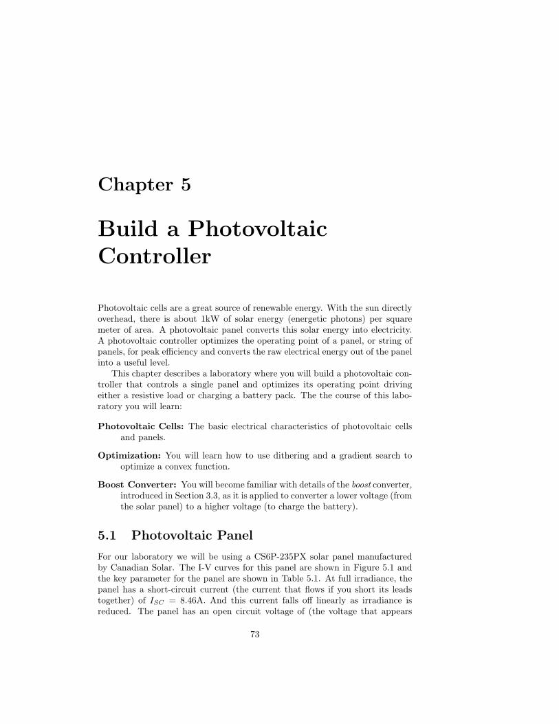
Chapter 5
Build a PhotovoltaicController
Photovoltaic cells are a great source of renewable energy. With the sun directlyoverhead, there is about 1kW of solar energy (energetic photons) per squaremeter of area. A photovoltaic panel converts this solar energy into electricity.A photovoltaic controller optimizes the operating point of a panel, or string ofpanels, for peak efficiency and converts the raw electrical energy out of the panelinto a useful level.
This chapter describes a laboratory where you will build a photovoltaic con-troller that controls a single panel and optimizes its operating point drivingeither a resistive load or charging a battery pack. The the course of this labo-ratory you will learn:
Photovoltaic Cells: The basic electrical characteristics of photovoltaic cellsand panels.
Optimization: You will learn how to use dithering and a gradient search tooptimize a convex function.
Boost Converter: You will become familiar with details of the boost converter,introduced in Section 3.3, as it is applied to converter a lower voltage (fromthe solar panel) to a higher voltage (to charge the battery).
5.1 Photovoltaic Panel
For our laboratory we will be using a CS6P-235PX solar panel manufacturedby Canadian Solar. The I-V curves for this panel are shown in Figure 5.1 andthe key parameter for the panel are shown in Table 5.1. At full irradiance, thepanel has a short-circuit current (the current that flows if you short its leadstogether) of ISC = 8.46A. And this current falls off linearly as irradiance isreduced. The panel has an open circuit voltage of (the voltage that appears
73
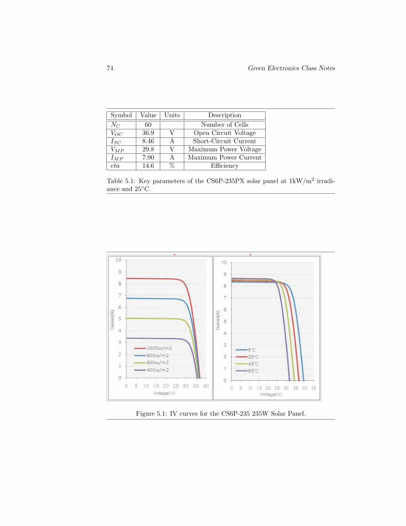
74 Green Electronics Class Notes
Symbol Value Units DescriptionNC 60 Number of CellsVOC 36.9 V Open Circuit VoltageISC 8.46 A Short-Circuit CurrentVMP 29.8 V Maximum Power VoltageIMP 7.90 A Maximum Power Currenteta 14.6 % Efficiency
Table 5.1: Key parameters of the CS6P-235PX solar panel at 1kW/m2 irradi-ance and 25C.
Figure 5.1: IV curves for the CS6P-235 235W Solar Panel.

Copyright (c) 2011 by W.J Dally, all rights reserved 75
RSHISC
RS
D1 VC
+
_
D2
Figure 5.2: Model of a single photovoltaic cell.
across its terminals with no current flowing) of VOC = 36.9V. The open circuitvoltage is reduced slightly as irradiance is reduced but is a strong function oftemperature.
The current is initially very flat, holding relatively steady as voltage is in-creased until about 30V. At that point the current is drops exponentially withvoltage. The peak power point, the point where the power (the product ofvoltage and current) is a maximum is at the knee of this curve.
Figure 5.2 shows a circuit model of a single photovoltaic cell. We modelthe cell as a current source — that represents the photocurrent generated byenergetic photons — in parallel with two diodes. The diodes have differentcharacteristics, one is nearly ideal with an emissivity constant n = 1 and ISat =3×10⁻¹⁰ while the other represents losses due to recombination and other effectsand hence has an emissivity constant of n = 3 and ISat = 5× 10⁻⁴. The shuntresistor RSH sets the slope of the horizontal part of the current curve at lowvoltages. The series resistor RS sets the slope of the vertical part of the currentcurve at low currents.
5.2 Power Path
Figure 5.3 shows the power path of the PV controller, a simple boost converter(Section 3.3). The PV panel provides energy at its operating voltage VPV andcurrent IPV , which is sensed across resistor RS . Input capacitor Ci stores thisenergy to smooth the inductor ripple current. Current in inductor L1 rampsup when MOSFET M1 is on and ramps down — transferring its energy to thehigher load voltage VL — when M2 is on. Output capacitor CO smooths theoutput load current.
As derived in Section 3.3 the duty factor D of M1 determines the voltageratio.
VL
VPV=
11−D
(5.1)
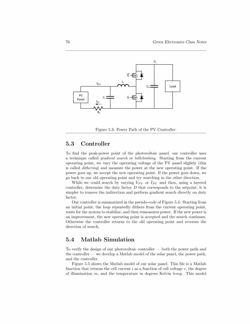
76 Green Electronics Class Notes
Ci
VPV
PV Panel
RS
M1G
CO
L1
Load
M2G
VL
IPV
Figure 5.3: Power Path of the PV Controller.
5.3 Controller
To find the peak-power point of the photovoltaic panel, our controller usesa technique called gradient search or hillclimbing. Starting from the currentoperating point, we vary the operating voltage of the PV panel slightly (thisis called dithering) and measure the power at the new operating point. If thepower goes up, we accept the new operating point. If the power goes down, wego back to our old operating point and try searching in the other direction.
While we could search by varying VPV or IPV and then, using a layeredcontroller, determine the duty factor D that corresponds to the setpoint, it issimpler to remove the indirection and perform gradient search directly on dutyfactor.
Our controller is summarized in the pseudo-code of Figure 5.4. Starting froman initial point, the loop repeatedly dithers from the current operating point,waits for the system to stabilize, and then remeasures power. If the new power isan improvement, the new operating point is accepted and the search continues.Otherwise the controller returns to the old operating point and reverses thedirection of search.
5.4 Matlab Simulation
To verify the design of our photovoltaic controller — both the power path andthe controller — we develop a Matlab model of the solar panel, the power path,and the controller.
Figure 5.5 shows the Matlab model of our solar panel. This file is a Matlabfunction that returns the cell current i as a function of cell voltage v, the degreeof illumination m, and the temperature in degrees Kelvin temp. This model
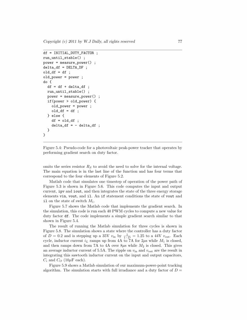
Copyright (c) 2011 by W.J Dally, all rights reserved 77
df = INITIAL_DUTY_FACTOR ;run_until_stable() ;power = measure_power() ;delta_df = DELTA_DF ;old_df = df ;old_power = power ;do df = df + delta_df ;run_until_stable() ;power = measure_power() ;if(power > old_power) old_power = power ;old_df = df ;
else df = old_df ;delta_df = - delta_df ;
Figure 5.4: Pseudo-code for a photovoltaic peak-power tracker that operates byperforming gradient search on duty factor.
omits the series resistor RS to avoid the need to solve for the internal voltage.The main equation is in the last line of the function and has four terms thatcorrespond to the four elements of Figure 5.2.
Matlab code that simulates one timestep of operation of the power path ofFigure 5.3 is shown in Figure 5.6. This code computes the input and outputcurrent, ipv and iout, and then integrates the state of the three energy storageelements vin, vout, and il. An if statement conditions the state of vout andil on the state of switch M1.
Figure 5.7 shows the Matlab code that implements the gradient search. Inthe simulation, this code is run each 40 PWM cycles to compute a new value forduty factor df. The code implements a simple gradient search similar to thatshown in Figure 5.4.
The result of running the Matlab simulation for three cycles is shown inFigure 5.8. The simulation shows a state where the controller has a duty factorof D = 0.2 and is stepping up a 35V vin by 1
1−D = 1.25 to a 44V vout. Eachcycle, inductor current iL ramps up from 4A to 7A for 2µs while M1 is closed,and then ramps down from 7A to 4A over 8µs while M2 is closed. This givesan average inductor current of 5.5A. The ripple on vin and vout are the result inintegrating this sawtooth inductor current on the input and output capacitors,Ci and CO (10µF each).
Figure 5.9 shows a Matlab simulation of our maximum-power-point trackingalgorithm. The simulation starts with full irradiance and a duty factor of D =

78 Green Electronics Class Notes
function [i] = pv(v,m,temp)% model of a PV cell% i is current% v is voltage% m is illumination - 0-dark, 1-full sunlight% temp is temperature in degrees K
% ignore Rs and find current from diodes and Rshrsh = 300 ; % shunt resistanceis1 = 5e-4 ; % diode 1 parametersdn1 = 3 ;is2 = 3e-10 ; % diode 2 parametersdn2 = 1 ;cells = 60 ; % number of cells in seriesk = 1.38E-23 ;q = 1.6E-19 ;ve = k*temp/q ;
igen = 8.46*m ;
i = igen - v/rsh - is1*(exp(v/(cells*dn1*ve))-1) - is2*(exp(v/(cells*dn2*ve))-1) ;
Figure 5.5: Matlab model of our solar panel.
% simulate one step, dt of PV power path% if a switch is down, otherwise switch is upipv = pv(vin,illum) ;iout = vout/rout ;if(a)dil = vin*dt/l1 ;dvout = -iout*dt/cout ;
elsedil = (vin-vout)*dt/l1 ;dvout = (il - iout)*dt/cout ;
endvin = vin + (ipv - il)*dt/cin ;vout = vout + dvout ;il = il + dil ;
Figure 5.6: Matlab code to advance the state of the power-path of Figure 5.3one time step.
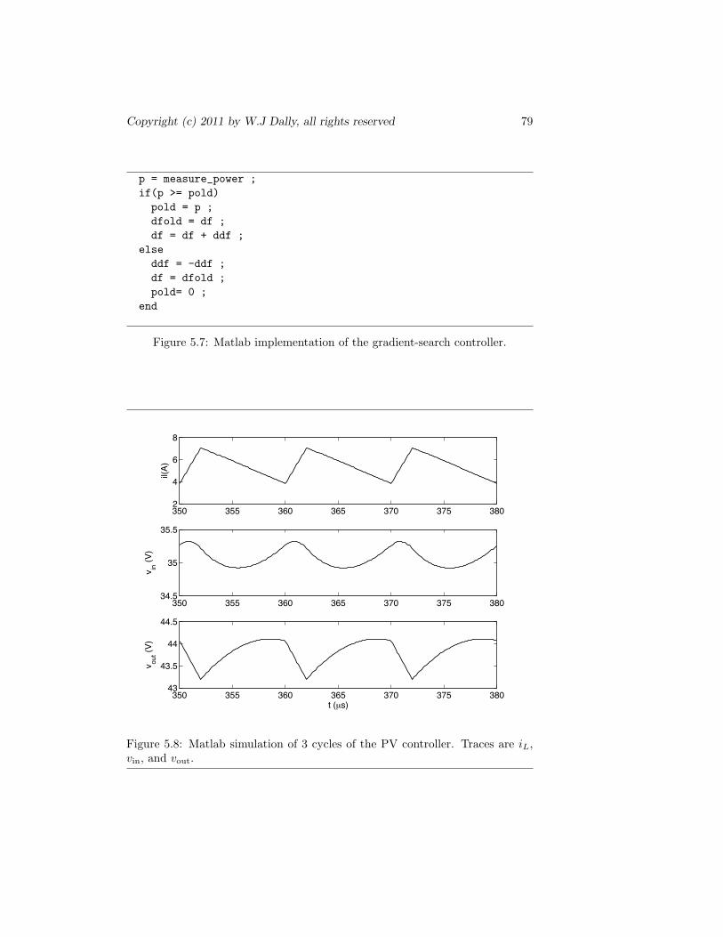
Copyright (c) 2011 by W.J Dally, all rights reserved 79
p = measure_power ;if(p >= pold)pold = p ;dfold = df ;df = df + ddf ;
elseddf = -ddf ;df = dfold ;pold= 0 ;
end
Figure 5.7: Matlab implementation of the gradient-search controller.
350 355 360 365 370 375 3802
4
6
8
il(A)
350 355 360 365 370 375 38034.5
35
35.5
v in (V
)
350 355 360 365 370 375 38043
43.5
44
44.5
v out (V
)
t (µs)
Figure 5.8: Matlab simulation of 3 cycles of the PV controller. Traces are iL,vin, and vout.
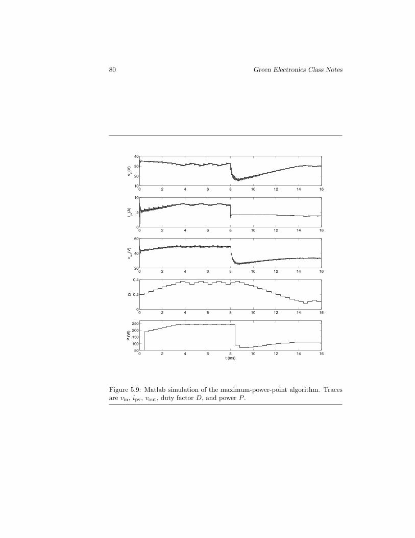
80 Green Electronics Class Notes
0 2 4 6 8 10 12 14 1610
20
30
40
v in(V
)
0 2 4 6 8 10 12 14 160
5
10
i pv(A
)
0 2 4 6 8 10 12 14 1620
40
60
v out(V
)
0 2 4 6 8 10 12 14 160
0.2
0.4
D
0 2 4 6 8 10 12 14 1650
100150200250
P (W
)
t (ms)
Figure 5.9: Matlab simulation of the maximum-power-point algorithm. Tracesare vin, ipv, vout, duty factor D, and power P .

Copyright (c) 2011 by W.J Dally, all rights reserved 81
* SPICE model of the power pathx1 an ca pv_panel
RS ca 0 0.01CI an 0 ciL1 an x 22uH
xf2 l g2 x irlb3036pbfxf1 x g1 0 irlb3036pbf
CO l 0 coRL l 0 10
Figure 5.10: SPICE model of the power path of Figure 5.3.
0.2. Half-way through the simulation, at 8ms, irradiance is abruptly reduced to50%.
During the first 4ms of the simulation, D ramps from its initial value of 0.2which yeilds a power of about 190W to a value of 0.36 where power reachesa peak of about 240W. The simulation spends the next 4ms dithering aboutthe optimal value with duty factor varying between 0.34 and 0.38. Because thepower curve is fairly smooth in this area, power holds steady at about 240W.
At 8ms the irradiance is abruptly cut in half. This cuts the panel currentroughly in half - from about 8A to about 4A and both the input and outputvoltage fall in response. This puts the panel at a very non-optimal operatingpoint — due to its low input voltage — about 18V.
The peak-power tracking algorithm responds to the transient by ramping Ddown to 0.1 at about 14ms. This ramps the input voltage back up to about 30Vgiving a power P of about 110W. The controller then dithers about this newoptimal point with D varying between 0.08 and 0.12.
5.5 SPICE Simulation
Matlab is useful for understanding the high-level operation of the PV controllerand for simulating the control algorithm along with the circuit. SPICE, onthe other hand, is useful for exploring the details of circuit operation includingswitching losses, transient currents, and stresses on components.
A SPICE model of the power path of Figure 5.3, including the photovoltaicpanel and a resistive load, is shown in Figure 5.10. Subcircuit x1 is the pho-tovoltaic panel and subcircuits xf1 and xf2 are M2 and M1. The model alsoincludes the inductor L1 input capacitor CI, output capacitor, CO, load resistorRL, and sense resistor RS.
Figure 5.11 shows a SPICE simulation of two cycles of the power path ofFigure 5.10. The waveforms closely match those of Figure 5.8 although the
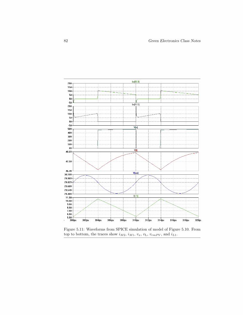
82 Green Electronics Class Notes
Figure 5.11: Waveforms from SPICE simulation of model of Figure 5.10. Fromtop to bottom, the traces show iM2, iM1, vx, vL, vrmPV , and iL1.
Copyright (c) 2011 by W.J Dally, all rights reserved 83
operating point here has a higher duty factor (0.4). During the first portionof each cycle inductor, vX is zero and inductor current ramps up through M1.During the second portion of each cycle, vX is equal to vL and inductor currentramps down through M2.
The top two traces show a large current transient when M1 turns on. Thiseffect is due to the reverse recovery time of the body diode in M2. When M2
turns off, the body diode of M2 carries the inductor current until M1 turns on.When M1 turns on, it sinks the inductor current to ground and reverse biasesthe body diode of M2. However, it takes several nanoseconds for this diode toturn off. During these few nanoseconds, M1 shorts vL to ground and draws avery large current.
Figure 5.12 shows a close-up of the M1 turn-on transient. The figure showsthat because of the slow diode reverse-recovery, current in M1 (and M2) rampsto over 150A while the voltage across M1 is still over 44V. This shoot-throughcurrent occurs because M1 and the body diode of M2 are both on at the sametime — effectively shorting vL to ground. At the peak of the current transient,the instantaneous power dissipated in M1 reaches nearly 7kW. Fortunately thislasts for only a few nanoseconds. The total energy of this transient Eon, the areaunder the power curve, is 29µJ (as measured with a SPICE .measure statement.With a switching frequency of 100kHz, this gives a switching loss due to theM1-on transient of 2.9W. There is also a 7.4µJ loss in M2.
The M2 turn-on-transient, shown in Figure 5.13 is much less dramatic. AsM1 turns off, and the current in M1 (bottom trace) ramps down, the body diodeof M2 turns on instantly and picks up the remainder of the inductor current iL.Thus, as iM1 ramps from 11A to 0A iM2 ramps from 0A to 11A. Voltage vx
swings from 0V to 48V during this 70ns period. The PM1 peaks at about 180Wand PM2 peaks at about 90W. The energy during this transient Eoff is 9.2µJfor M1 and 4.6µJ for M2 for a total of 13.8µJ or 1.3W at 100kHz.
The total switching losses over both M1 and M2 over both the on transitionof Figure 5.12 and the off transition of Figure 5.13 is 49µJ or 4.9W at 100kHz.These switching losses can be largely eliminated by using soft-switching tech-niques. There are also conduction losses in the transistors and inductors thatwe are not considering here.
Of course, the results of this SPICE simulation are only as good as themodels that went into it. This simulation used manufacturers models for theMOSFETs. However parasitic inductance due to board layout was ignored. Ifthis inductance is significant, it can make a very large difference to the switchinglosses. A truly accurate simulation would include parasitic circuit elementscalculated from layout geometry and validated via experiment.
5.6 The Laboratory
For the laboratory you are to do the following.
1. Build a Matlab model of the PV controller and simulate operation of the

84 Green Electronics Class Notes
Figure 5.12: Close-up of the M1 turn-on transient. Traces are PM1, vx (voltageat the drain of M1), iM2, and iM1.
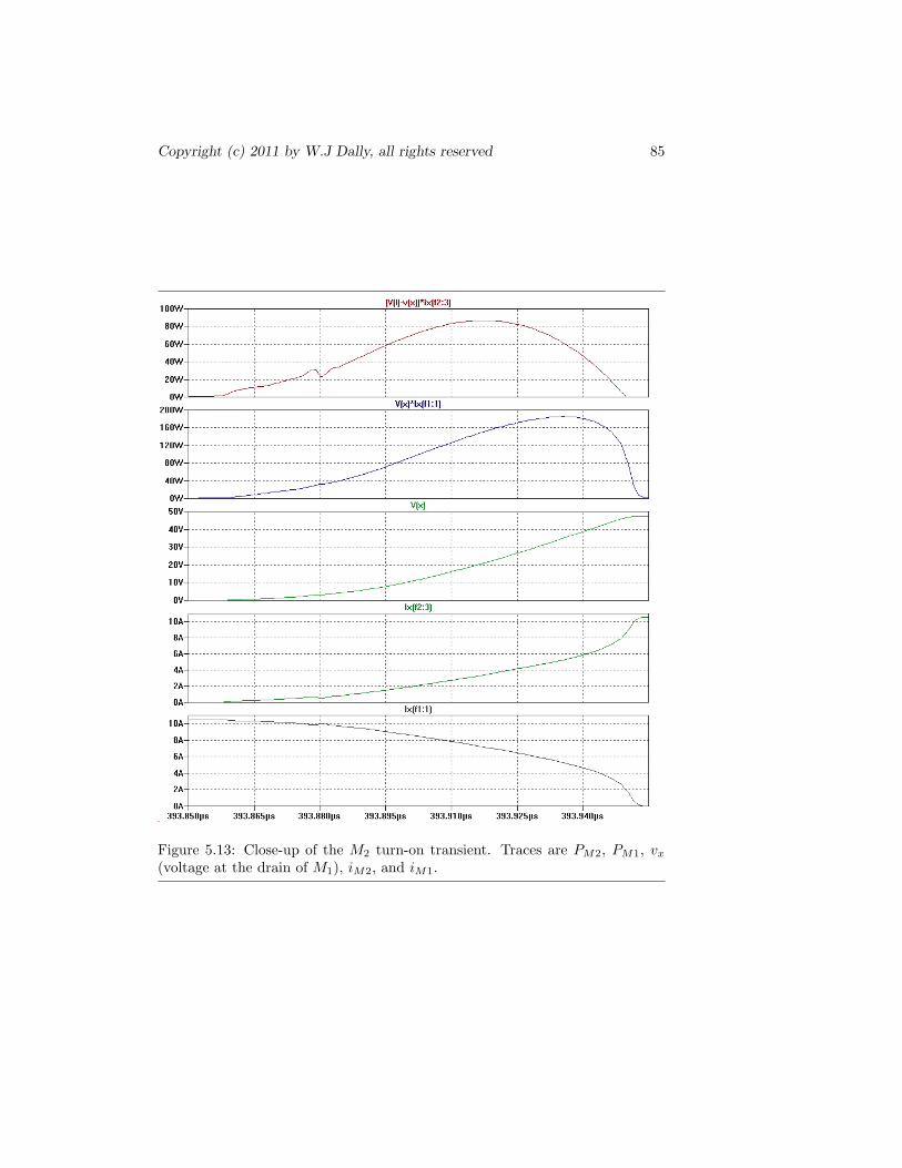
Copyright (c) 2011 by W.J Dally, all rights reserved 85
Figure 5.13: Close-up of the M2 turn-on transient. Traces are PM2, PM1, vx
(voltage at the drain of M1), iM2, and iM1.

86 Green Electronics Class Notes
controller including finding the maximum-power point and dealing withtransients in irradiance and temperature.
2. Buld a SPICE model of the PV controller and simulate five cycles ofoperation in a steady state conditions. Measure the energy of the turn-onand turn-off transients.
3. Wire up the power path of Figure 5.3 and control it using a 100kHz PWMsignal from teh processor module. Write the embedded code to performthe maximum-power point tracking.
4. Test your prototype PV controller using a lab power supply set for 30Vmaximum voltage and 3A maximum current to simulate a PV panel (albeitwith a rather square I-V curve. Your maximum-power point tracker shouldfind the pulse width needed to stay at this maximum power point.
5. Test your prototype PV controller using an actual solar panel. Verify thatit finds a new maximum-power point when you shade half of your panelwith a piece of cardboard.
6. (Optional) Measure the efficiency of your PV controller by placing energymeters before and after the controller.
5.7 Extensions
Inverter: Modify your PV controller to include an inverting output stage to in-terface with a power line. The boost stage of Figure 5.3 should be modifiedto produce an intermediate voltage that is larger than the maximum ACvoltage (170V for 110V AC and 340V for 220V AC). A full-bridge stageshould then be added to synthesize a sine wave via pulse-width modu-lation. An LC output filter is needed to filter out the PWM frequencynoise.
Panel Balancing: If two PV panels (or two PV cells) connected in a stringare not identical or do not have identical irradiance, it will not be possibleto simultaneously find the maximum-power point for both. The currentiPV which is common to all of the panels in a string will be a compromisebetween the maximum-power current of the two panels.
Using our Matlab model for a solar panel, quantify the amount of powerlost when two panels must operate at the same current point when one hasan full irradiance (1000W/m2) and the other has half irradiance (500W/m2)compared to the power when both are operated at their individual maximum-power points.
The current of each panel (or cell) in a string can be made individuallyadjustable by using a pulse-width-modulated inductor to losslessly bypasscurrent around panels requiring a lower current. Design such a panelbypass circuit and simulate it in SPICE on a two-panel configuration.

Copyright (c) 2011 by W.J Dally, all rights reserved 87
(Optional) Implement your circuit and demonstrate it on a real two panelconfiguration with one panel half shaded.
Variable-Step Gradient Search: Our gradient-search algorithm has a fixedstep size. This causes it to take a long time to track a large transientand at the same time results in a fairly large dithering region once weare converged on the maximum-power point. Develop a better searchalgorithm that varies the step size for faster tracking of transients andsmaller dithering intervals when converged.
Soft Switching: As illustrated in Figure 5.12 and Figure 5.13, our PV con-troller power path performs hard switching, resulting in significant switch-ing losses. By switching our MOSFETs only when the current throughthem is zero (zero-current switching or ZCS), or the voltage across them iszero (zero-voltage switchign or ZVS), or both, we can reduce the switchinglosses to zero.
Design a power path that uses soft switching to eliminate switching lossesand simulate this power path using SPICE. Measure the total losses —switching, MOSFET conduction, and inductor conduction and core losses— for both the original configuration and your new design.
(Optional) Implement your design and demonstrate it operating with aPV panel. Measure its efficiency using an energy meter before and afterthe PV controller.
Stability Analysis: We use a 10µF film capactior for Ci because it reducesvoltage ripple due to the inductor current ripple to acceptable levels. Itturns out that if this capacitor is made very large, say 1mF, the PV con-troller will oscillate. Develop a model of the PV controller that allows youto study its stability. Using your model, predict the value of capacitancethat causes the controller to oscillate. Develop a strategy to stabilize thecontroller when using a large capacitor.

88 Green Electronics Class Notes

Appendix A
Safety
If a few basic rules are followed a power electronics laboratory exercise canbe completed in a safe manner — with little risk of injury or damage to equip-ment. However, because of the high voltages, currents and power levels involveddeviation from the rules or careless activity has the potential to cause harm.
This appendix outlines the risks associated with a power electronics labora-tory and a set of rules and procedures to manage these risks without incident.
A.1 Risks
The risks associated with a power electronics lab an inherent to working withhigh-voltage, high-current electronics and include:
Electric Shock: Some conductors in the circuits you will build will be at highvoltages (up to several hundred volts). Touching these conductors withyour bare hands or with a conductive tool can result in a severe electricshock.
The capacitors in the circuits you will build store many Joules of energyand can retain this energy even when the circuit is powered down. Do notassume it is safe to touch a circuit just because the power is turned off.Always make sure high energy capacitors have been drained.
Burns: Some components in power electronic systems dissipate large amountsof power in the form of waste heat. Because of finite thermal resistance,these components get hot — often as much as 100-200C. It can take manyminutes after a circuit is powered down for hot components to cool off.Touching a hot component can result in a severe burn.
During failures of power circuits wires and other conductors may get sohot that they vaporize. If your hand — or other body part — is nearthese conductors when they vaporize you can suffer a plasma burn.
89

90 Green Electronics Class Notes
Projectiles: An incorrectly operating power circuit can overheat a componentcausing it to explode and eject fragments with high velocity. Power semi-conductors, power resistors, capacitors, and inductors can all exhibit thisbehavior if they are overloaded. If a part of your body gets in the pathof a fragment of an exploding component you can suffer an injury. Youreyes are particularly vulnerable.
A.2 Rules and Procedures
To manage the risks associated with a power electronics lab, we follow a fewsimple rules and procedures. Please take these seriously — ignoring the rulesor taking shortcuts can result in someone getting hurt — possibly you.
Don’t work alone: A minor injury can become life threatening if there is noone present to lend aid and call for help. Never work in the lab by yourselfon high-power circuits.
For EE26N we carry this one step further by opening the lab only whenit is supervised by an instructor or section leader.
Don’t work if you are not at your best: If you are tired, sick, distractedby a situation outside the lab, inebriated, or otherwise operating at lessthan 100% of your mental capacity, don’t work in the lab. Accidentshappen when people aren’t completely focused on what they are doingwith all of their faculties.
Don’t “operate” on a powered circuit: Do not attempt to rewire a circuit,apply or move a prove, or any other manipulation of a power circuit whileit is powered on. With the lid closed while power is applied you shouldn’tbe able to do this anyway. Moving a probe or a wire is a good way tocause a momentary short that can vaporize the wire and give you a nastyplasma burn.
Close the lid before applying power: To protect you from vaporizing wiresand exploding components, our Green Electronics lab kits have plexiglasslids. These lids let you see your circuit while protecting you from flyingdebris. However, they will only work if they are down when the explosionhappens, so lower the lid before applying power.
Wear eye protection when power is applied: On the off chance that a par-ticularly energetic explosion escapes the lid, wear eye protectin when cir-cuits are powered on — either regular eyeglasses or safety glasses.
Check component temperatures before touching: Before touching a powercomponent, use the infrared thermometer — not your finger — to checkits temperature. Wait until all components have cooled to less than 40C(104F) before touching anything.

Copyright (c) 2011 by W.J Dally, all rights reserved 91
Check capacitor voltages before touching: Large capacitors can hold a sig-nificant charge for weeks. The Green Electronics modules have bleeder re-sistors on these capacitors to discharge them in a few minutes, but don’tassume they are functioning. Either check a capacitor with a voltmeter,or short it to ground with a 25W 1K resistor (which will discharge a 1mFcapacitor in a few seconds) before operating.
While less important from a safety perspective, the following guidelines willavoid uneccesary destruction of lab equipment:
Low-power first: Before hooking a lab to the 48V 100A (4.8kW) battery packor to the 110V 15A (1.65kW) AC mains hook it up to a lab supply thatcan provide moderate voltage with a current limit. This will let you find acircuit problem without having the problem cause your circuit to destroyitself — leaving few clues of what went wrong.
Pulsed power second: Once your circuit is working on a lab power supplyhook it to the high-power supply (battery or AC mains depending on thelab) and pulse the supply on and then quickly off. You should power thecircuit just long enough to take a measurement with the oscilloscope. Afterpowering down, check component temperatures. If everything is workingas expected, power it on for a bit longer and check again. Repeat withlonger time intervals until you are comfortable with steady-state operation.
Understand the startup transient: Many problems with power circuits hap-pen during the transient when either the input power or the load is applied.An inrush of current when input power is applied can overload conductorsor components and with parasitic inductance in the input path can leadto over-voltage conditions as well. Control systems are sometimes peggedin a full-on state when the input power is off leading to exessive currentflow when power is first applied — particularly if the controller is slow torespond. Make sure you understand the transient behavior of your cir-cuit during key transitions. It is a good idea to trigger a scope on eachtransient of interest to capture a “picture” of your circuit’s behavior.
Make sure your controller is stable: Many other problems with power cir-cuits stem from control problems. An unstable controller can easily drivea circuit to destruction. Make sure your controller is stable. Its also agood idea to put in one or more fail-safe checks that shut the circuit downif an out-of-limit condition is detected.
Understand a failure before trying again: Repeating an action and expect-ing a different response is the operational definition of insanity. If youpower on your circuit and it explodes, don’t just replace the burned-outparts and try again. Think. Understand what caused the failure andredesign (or reprogram) your circuit to fix the problem. If you don’t un-derstand the failure — and there’s not enough of your circuit left to figureout what failed first — plan a low-power experiment to verify operationbefore attempting another high-power trial.

92 Green Electronics Class Notes
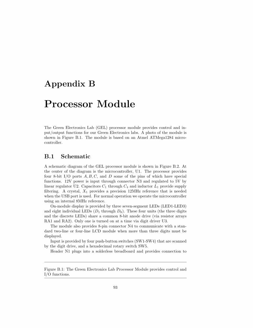
Appendix B
Processor Module
The Green Electronics Lab (GEL) processor module provides control and in-put/output functions for our Green Electronics labs. A photo of the module isshown in Figure B.1. The module is based on an Atmel ATMega1284 micro-controller.
B.1 Schematic
A schematic diagram of the GEL processor module is shown in Figure B.2. Atthe center of the diagram is the microcontroller, U1. The processor providesfour 8-bit I/O ports A,B, C, and D some of the pins of which have specialfunctions. 12V power is input through connector N3 and regulated to 5V bylinear regulator U2. Capacitors C1 through C4 and inductor L1 provide supplyfiltering. A crystal, X1 provides a precision 12MHz reference that is neededwhen the USB port is used. For normal operation we operate the microcontrollerusing an internal 8MHz reference.
On-module display is provided by three seven-segment LEDs (LED1-LED3)and eight individual LEDs (D1 through D8). These four units (the three digitsand the discrete LEDs) share a common 8-bit anode drive (via resistor arraysRA1 and RA2). Only one is turned on at a time via digit driver U3.
The module also provides 8-pin connector N4 to communicate with a stan-dard two-line or four-line LCD module when more than three digits must bedisplayed.
Input is provided by four push-button switches (SW1-SW4) that are scannedby the digit drive, and a hexadecimal rotary switch SW5.
Header N1 plugs into a solderless breadboard and provides connection to
Figure B.1: The Green Electronics Lab Processor Module provides control andI/O functions.
93
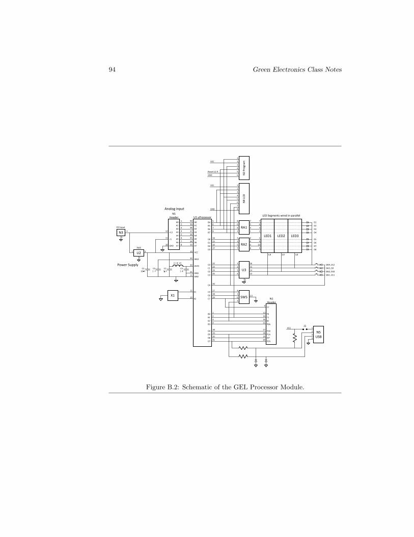
94 Green Electronics Class Notes
40A0
39 A138 A237 A336 A435 A534 A633 A7
30 AVCC
33 AREF
10 VCC
31
11
C31 F
C41 F
C11 F
L1 10 H
C210 F
GND
GND
A0
A1
A2
A3
A4
A5
A6
A7
1
2
3
4
5
6
7
8
Analog input
U2
7805
N3
1 3
2
3
1
12V input
N1 Header
10
11
12
GND
+5
+12
U1 uProcessor
RA1
B4
B5
B6
Power Supply
B7
D0
D1
D2
D3
5
1
2
VCC
8 7
6
7
8
14
6 5
N4
LC
D
3
4
5
6
7
8
N2
Pro
gram
1
2VCC
3
4
5
6
GND
4 3
2 1
RA217
15
16
1
3
5
7
2
4
6
8
LED1 LED2 LED3
GND
C0
C1
C2
C3
22
25
23
24
1
2
3
4
U3
16
D1
D8
D2
D3
D4
D5
D6
D7
15
LED Segments wired in parallel
3,83,8 3,8
14
13
Reset U1-9
SW4, D12
SW3, D9
SW2, D10
SW1, D11
26C4
8
7
6
4
2
1
9
5
10
C5
C6
C7
27
28
29 SW5 2,51
4
6
B0
B1
B2
B3
N1 Header
1T0
2
13
3
14T1
4
3
16B2
15P0A
D7
D4
D5
D6
18 17P1B
19 18P1A
20
21
19
20P2A
ICP
N5USB
1
2
J1VCC
3
4
X1
X2
X1
12
13
9C7
Figure B.2: Schematic of the GEL Processor Module.

Copyright (c) 2011 by W.J Dally, all rights reserved 95
selected port pins of the microprocessor. The first eight pins of the headerconnect to processor port A (A0 to A7). These pins can (among other functions)be configured as analog inputs to an A/D converter. Pins 10-12 of the headerbring out the three power supplies on the module (GND, +5V, and +12V). Theremaining pins bring out selected pins of other ports including the low Nybbleof port B and the high Nybble of port D. Some of these pins are shared withother functions.
B.2 Software
A software library is provided to simplify access to the functions of the processormodule. The following sections give an overview of the library. For details thereader should consult the source code.
Many of the library functions provide access to registers of the ATMega1284processor. For details of these registers and the functions of the processor’s A/Dand timer/counters, refer to the processor manual available online. 1
B.2.1 Display and Switch Input
To use the displays call lcd init() and led init() at the beginning of programexecution. Then call refresh display() once every 3ms. This will copy thevalues of arrays led[4] (segment data) and lcd[80] (ASCII characters) to thedisplays.
The preferred way to display data on the LED display is to use libraryroutine snprintf. For example, the following program fragment displays threevariables on the first line of the display and one variable on the second line.
snprintf(&lcd[0],SPN,"P%03d I%6d V%6d",pwm,current.value,voltage.value) ;snprintf(&lcd[20],SPN,"T%6d",temperature.value) ;lcd_fix_zeros() ;
snprintf does have the unfortunate side effect of writing a zero after thelast character of the string being printed. To deal with this, the display shouldbe written in order, so later writes overwrite any zeros from earlier writes thatwrapped to the next line. After all writes are complete the routine lcd fix zeros()replaces any zeros remaining with a space (hex 20).
The preferred way to display data on the seven-segment LED display is to uselibrary routines set hex display(start,nr,value) and set bcd display(start,nr,value).These routines take a 16-bit unsigned value and display it as nr digits startingfrom digit start. Arguments start and nr are unsigned 8-bit values. For ex-ample, the following call displays current.value as a decimal number on thethree LED digits:
set_bcd_display(0,3,current.value) ;
1At the time of writing, the processor manual was available athttp://atmel.com/dyn/resources/prod documents/doc8272.pdf.

96 Green Electronics Class Notes
If we would rather display the value in hexadecimal we use:
set_hex_display(0,3,current.value) ;
To update the discrete LEDs simply write the desired value to led[3].The state of the four pushbutton switches can be accessed by reading variable
pb. The value of the hex switch is returned as an eight-bit unsigned value byroutine hex in().
B.2.2 Real-Time Clock Interrupt
Most of our Green Electronics Labs are interrupt driven. The lab code is exe-cuted in response to processor interrupts. A real-time clock causes an interruptto occur at regular intervals to allow certain functions to be performed on aperiodic basis.
By convention we use timer/counter 2 of the ATMega1284 to generate real-time clock interrupts. To configure this counter, the user calls rtc2 init withthree arguments to set up registers TCCR2A, TCCR2B, and OCR2A. The user thendefines a routine rtc() that is called on each interrupt.
For example, to set up an interrupt once every 1ms, the counter is configuredwith the call
rtc2_init(TCCRA_CTC, TCCR2B_D32, OCR2A_1MS_D32) ;
The first argument configures the counter in CTC (clear timer on comparematch) mode. The second sets the counter source to divide the 8MHz processorclock by 32 - so the processor counts at 250kHz. The final argument sets thecounter to compare and cause an interrupt when it reaches 250 - which gives ainterrupt every 1ms.
To get an interrupt every 3ms the call is:
rtc2_init(TCCRA_CTC, TCCR2B_D1K, OCR2A_3MS_D1K) ;
Routine rtc() then defines what happens on each interrupt. This routinemight request A/D conversions, refresh the display, and count down to performother functions at longer periods.
For example, consider the following routine.
void rtc() adreq |= AD_0 ; // start conversion on channel 0if(adidle) start_ad() ;sei() ; // enable interruptsrefresh_display() ; // refresh LED and update LCDif(++timer_50 > TIME_50) // count down for 50ms routinet50=0 ;rtc50ms() ; // do this every 50ms

Copyright (c) 2011 by W.J Dally, all rights reserved 97
This routine requests an A/D conversion on channel 0 by ORing AD 0 intoadreq and then starting the converter if it is idle. Interrupts are then renabledto allow higher priority interrupts access to the processor while the remain-ing functions are performed. Next the displays are refreshed with a call torefresh display(). The final loop counts down to perform other real-timefunctions every 50ms in routine rtc50ms().
B.2.3 Analog Input
The ATMega1284 processor includes a 10-bit analog-to-digital (A/D) converter.The converter runs on a 125kHz clock (the 8MHz processor clock divided by64) and takes 13 cycles to perform a conversion, so just over 9 conversions canbe performed each 1ms.
To use the A/D converter, the programmer must first make a call to adc init()to configure the converter. Conversions are requested by ORing requests intobit-vector adreq, and then calling start ad() if adidle is true — as in thecode fragment in Section B.2.2 above.
When a conversion is complete, the A/D interrupt handler calls a user-defined routing corresponding to the request to handle the converted value whichis available in variable adcv. For the request AD 0 a routine ad 0() is called.The following code fragment shows an example ad 0() routine.
void ad_0() current.raw = adcv ;calibrate(¤t) ;
This routine copies the result of the conversion into the raw field of structurecurrent and then calls a calibration routine to compute a calibrated currentvalue.
B.2.4 PWM
For some of our labs we need to produce pulse-width modulated waveforms — adigital signal with a fixed frequency and a pulse-width that is varied as required.For our labs we will configure one or both of timer/counter 0 and timer/counter1 to generate PWM waveforms.
To use a timer/counter as a PWM generator, it is first configured with acall to an initialization routine. Then the pulse width is set by writing a controlvalue to the appropriate output compare register.
For example, to use timer/counter 0 to generate a 16kHz PWM signal onoutput A we first configure the counter with the following call:
pwm0_init(TCCRA_PWM, TCCRB_D1) ;
The first argument sets control register TCCR0A to select PWM mode withoutput A enabled. The second argument sets the counter to operate directly

98 Green Electronics Class Notes
off of the 8MHz processor clock. Because the 8-bit counter in PWM mode goesthrough 510 cycles for each pulse, this gives a pulse frequency of 15.69kHz.
To set the pulse width, we set register OCR0A. A value of zero produces aminimum-width pulse - 125ns wide. A value of 255 (hex FF) produces an outputthat is always high.
B.2.5 Calibration
The library provides a calibration function to facilitate calibrating inputs fromthe A/D converter. The function works with the following structure.
struct cal // value to be calibrateduint16_t raw ; // raw sampleuint16_t zero ; // raw value of zeroint32_t scale ; // multiplied by 2^16int16_t value ; // calibrated value
;
Calibration is performed by measuring the raw A/D values at two points,zero and a standard value. For example, suppose we have measured the rawA/D readings for voltage at zero (voltage zero) and 10V (voltage 10v) andthat we want our calibrated voltage to be in units of 100mV. We initialize thestructure with the following code.
voltage.zero = voltage_zero ;// 10V std, 0.1V resolutioncompute_scale(&voltage,voltage_10v, 100UL) ;
We set the zero point by just assigning to voltage.zero. The value of voltage.scaleis then computed by calling compute scale with the raw value of our calibrationmeasurement voltage 10v and the value we would like this to correspond to 100(since 10V is 100 100mV increments). The routine computes the appropriatescale factor and stores it in the structure.
Once the structure is initialized each time we wish to convert a raw mea-surement to a calibrated value we just assign the raw value and call calibrate.The calibrated value is stored in the value field of the calibration structure.For example, when we read from the A/D we can execute the following code:
voltage.raw = adcv ; // raw value read from A/Dcalibrate(voltage) ; // computes calibrated value in voltage.value
B.2.6 Filtering
To reduce measurement noise on slowly changing signals the library provides afilter structure and routine that implements an autoregressive moving average(ARMA) filter. The filter structure contains three fields:
Copyright (c) 2011 by W.J Dally, all rights reserved 99
struct filter // variables to implement ARMA filterint32_t running_avg ;// running averageint16_t filtered ; // last filtered valueuint8_t shift ; // amount to shift by
A 32-bit running average running avg holds the state of the filter. This value isshifted left by shift bits. The filtered field holds the last output of the filter.The shift field sets the time constant of the impulse response of the filter.
The filter function:
void filter(int16_t value, filterP f) f->running_avg = f->running_avg - f->filtered + value ;f->filtered = (f->running_avg) >> f->shift ;
performs the following calculation
yi =2s − 1
2syi−1 +
12s
xi (B.1)
where yi is the filter output at timestep i, xi is the filter input at timestep i,and s is the shift value.

100 Green Electronics Class Notes

Appendix C
Component Module
Figure C.1 shows a photograph of the Green Electronics component module. Aschematic diagram of the module is shown in Figure C.2. The module containsan AC input circuit with fuse, rectifier, and filter capacitor, a second capacitor,an inductor, a current sense resistor, and a current transformer.
Power connections to the module are made via 0.25-inch quick-connect tabs(sometimes called faston or blade connectors). Signal connections are made viaa 6-pin female header that accepts 22AWG solid hookup wire for connectionsto a solderless breadboard.
Each of the sub-modules are described in more detail in the following sections— in increasing order of complexity. For the individual components the readeris encouraged to consult the manufacturers data sheets for more details.
C.1 Current Sense Resistor
The current sense resistor, shown at the bottom left of Figure C.2 is simply a10mΩ 5W resistor (a TT Electronics open-air resistor, part number OAR5R010FLF).Power connections are made to the resistor via two quick-connect terminals la-beled Ra and Rb. Signal connections are available via two female header re-ceptacles with the same labels. This four-point connection to a current-senseresistor, called a Kelvin connection, allows a differential voltage to be measuredjust across the resistor — avoiding any parasitic voltage drops on the powerconductors leading to and from the resistor.
Figure C.1: Photograph of the Green Electronics Component Module.
101
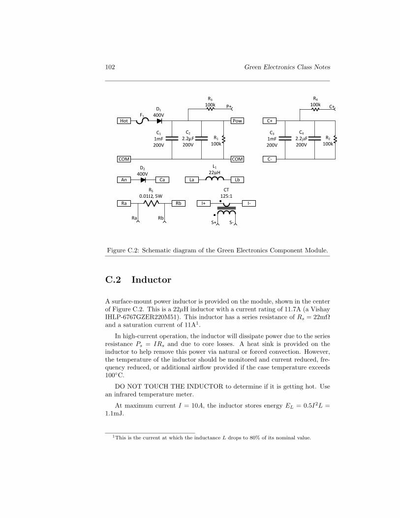
102 Green Electronics Class Notes
D1
400V
C1
1mF200V
F1
Hot
COM
C2
2.2 F200V
COM
Pow
C3
1mF200V
C4
2.2 F200V
C-
C+
D2
400VAn Ca La Lb
Ra Rb
L1
22 H
CT125:1
I+ I-
RS
0.01 , 5W
Ra RbS+ S-
R1
100k
R3
100k P+
R4
100k C+
R2
100k
Figure C.2: Schematic diagram of the Green Electronics Component Module.
C.2 Inductor
A surface-mount power inductor is provided on the module, shown in the centerof Figure C.2. This is a 22µH inductor with a current rating of 11.7A (a VishayIHLP-6767GZER220M51). This inductor has a series resistance of Rs = 22mΩand a saturation current of 11A1.
In high-current operation, the inductor will dissipate power due to the seriesresistance Ps = IRs and due to core losses. A heat sink is provided on theinductor to help remove this power via natural or forced convection. However,the temperature of the inductor should be monitored and current reduced, fre-quency reduced, or additional airflow provided if the case temperature exceeds100C.
DO NOT TOUCH THE INDUCTOR to determine if it is getting hot. Usean infrared temperature meter.
At maximum current I = 10A, the inductor stores energy EL = 0.5I2L =1.1mJ.
1This is the current at which the inductance L drops to 80% of its nominal value.
Copyright (c) 2011 by W.J Dally, all rights reserved 103
C.3 Diode
A 400V 20A diode is provided on the module, shown at the center left of Fig-ure C.2 and is accessed via quick-connect tabs labeled Anode and Cath. Thecurrent batch of component boards uses an NXP BYT79X-600,127 for this com-ponent, which is actually a 600V 40A diode with a 55ns reverse recovery time,a maximum forward voltage of 1.9V, and a maximum reverse leakage current of200µA.
C.4 Capacitor
The capacitor unit, at the upper right of Figure C.2 includes a 1mF 200V alu-minum electrolytic capacitor C3, a 2.2µF 200V film capacitor C4, a 100kΩdrainresistor R2, and a 100kΩsense resistor R4. The two capacitors and the drainresistor are connected in parallel and to two quick-connect tabs, labeled C+and C−. The sense resistor connects the positive terminal of the capacitors toone of the female header sockets, labeled C+.
Capacitor C3 is a 1mF 200V aluminum electrolytic capacitor (PanasonicEET-ED2D102CA). This part has an effective series resistance of Rs = 0.149Ωamaximum ripple current of Ir = 2.84A and a lifetime of 3,000 hours at 105C. Tofirst approximation, the lifetime doubles for each 10C reduction in temperaturebelow this point.
When selecting a capacitor for energy storage in a green electronics appli-cation the series resistance and ripple current limits are often as important, ifnot more important, than the actual capacitance. The lifetime rating is alsocritical. Electrolytic capacitors often limit the reliability of green electronic sys-tems. To design a system to operate 10 years (about 80,000 hours) for example,with a 3,000 hour at 105C capacitor, one must ensure the temperature of thecapacitor remains below 57C.
The series resistance of C3 gives it a pole at f = 12πRC 1kHz. The overall
impedance of the capacitor is the sum of its resistive and capacitive impedanceZC(s) = Rs + 1
Cs . Below 1kHz, this impedance is dominated by the capaci-tance. Above 1kHz the resistive term dominates. Above a few 100kHz parasiticinductance dominates.
To provide capacitance above 1kHz, we place film capacitor C4 in parallelwith C3. Capacitor C4 is a 2.2µF (Panasonic ECQ-E2225KF). This capacitorhas negligible series resistance, but its leads have a series inductance of about10nH. This gives it a resonant frequency of f = 1
2π√
LC1MHz. Above this
frequency the impedance of C4 is dominated by its inductance.Drain resistor R2 is provided to drain the charge off of C3 (and C4) when
not in use. When fully charged to V = 200V, C3 contains EC = 0.5CV 2 =20Jof energy. This could deliver a nasty shock even hours after the circuit is dis-connected. To prevent this, R2 drains the energy from C3 with a time constantof τ = RC = 100s. Because of this long time constant one should WAIT ATLEAST 5 min (3τ) before touching the capacitor terminals after powering the
104 Green Electronics Class Notes
circuit down.Sense resistor R4 is intended to form the upper branch of a voltage divider
to sense the voltage on the capacitor. For example, to scale a 200V voltageto a the 2.5V range of the A/D requires a divider with an 80:1 ratio. Using apull-down resistor with the standard value of 1.2kΩ gives a ratio of 84.3:1 whichwill suffice. The 100kΩresistor limits the current that flows if the sense lead isdisconnected from the bottom branch of the voltage divder or shorted to groundto about 2mA.
C.5 Current Transformer
The current transformer is a small transformer with a 1-turn primary and a 125-turn secondary that provides moderate frequency isolated current measurement.When a current is passed through the primary of the transformer — accessedvia quick-connect tabs I+ and I−, a current 125-times smaller appears betweenheader terminals S+ and S− which can be sensed via a small-valued resistor.To avoid negative voltages a diode is often used in series with the sense resistor.
For example, a 20A current in the primary will cause a 10125 = 160mA current
to flow in the secondary. Using a 6.25Ω sense resistor will generate an 1V sensevoltage.
This particular transformer is an ICE CT04-125. It is rated for up to a20A primary current and has a secondary inductance of 2.2mH. The primaryinductance is given by LP = Ls
N2r
= 140nH. This primary inducance affects thecircuit being measured.
C.6 AC Input Circuit
The AC input circuit provides protection, rectification, and filtering for a 110VAC input. Capacitors C1 and C2 and resistors R1 and R3 are a copy of thecapacitor submodule. Refer to Section C.4 for a discussion of their function.
Fuse F1 (nominally 10A) provides circuit protection. Should their be adownstream short causing more than this amount of current to flow, this fusewill blow opening the input circuit and shutting off the current flow. However,even a fast-acting fuse may take a large fraction of a second to blow — morethan enough time for considerable damage to occur to the downstream circuitry.
Diode D1 is the same diode as used in the diode submodule (Section C.3).In this case, it is wired as a half-wave rectifier. When the hot AC input (theblack wire) is in the positive half of its cycle and at a voltage above Pow, D1 willconduct causing Pow to follow hot up to the top of its cycle (at about 170V). Atthat point the diode becomes reverse biased and shuts off until the next cycle.At the point where hot is at its most negative voltage (-170V), there can be asmuch as 340V across the reverse-biased diode — hence the need for a minimumvoltage of 400V for this part.

Copyright (c) 2011 by W.J Dally, all rights reserved 105
The capacitors are used to filter the half-wave AC input. During the smallpart of the AC cycle when D1 conducts, C1 and C2 are charged to 170V. Duringthe remainder of the cycle, these capacitors supply current to the downstreamcircuit, partly discharging. To avoid overstressing the capacitor the downstreamcircuit should not draw more than Ir = 2.84A on average — higher peaks can beprovided by C2. To first approximation, C1 filters the AC input, storing energyduring the portion of the AC cycle when no current is being provided and C2
filters the higher frequency (often 200kHz) pulsed output current — allowingC1 to see the average of this current.

106 Green Electronics Class Notes

Appendix D
Half-Bridge Module
The half-bridge module is a push-pull driver stage that drives an output signalto either a power supply or ground. The driver uses power MOSFETs that arecapable of driving very high currents. For our motor lab, we will use this moduleconfigured with FETs capable of driving up to 195A with a series resistance ofRON = 2mΩ. A MOSFET driver allows these MOSFETs to be controlled withordinary logic signals.
A photograph of the module is shown in Figure D.1 and a schematic is shownin Figure D.2. The module drives the voltage from supply VD or common COM(another name for ground) onto the output Out via MOSFETs M1 and M2.Two quick-connect tabs are provided for each of these high-power signals.
A four-pin header plugs into a solderless breadboard to provide a +12Vsupply V12 signal ground GND high drive Hin and low-true low drive Lin’.An IRS21834 half-bridge driver converts these logic signals to higher-voltage,higher-current gate drive signals for the MOSFETs. Circuitry is included toprovide a floating bootstrap supply for the high side driver (the VB supply) andto filter the drain voltage to the half-bridge (the VD filter).
The remainder of this appendix describes each section in more detail.
D.1 Power MOSFETs
MOSFETs M1 and M2 perform the main function of the half-bridge moduleswitching the output between VD and COM. The major properties of the half-bridge module are inherited from the properties of these MOSFETs. For ourmotor controller and photovoltaic controller labs we use a version of the half-bridge module populated with IRLB3036. As described in Table M.1 this is a60V MOSFET with a typical on resistance RON of 2mΩand a maximum current
Figure D.1: Photograph of the Green Electronics Half-Bridge Module.
107
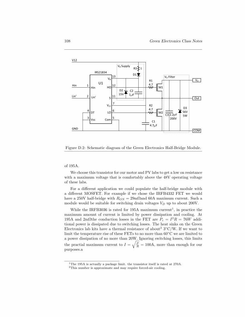
108 Green Electronics Class Notes
1
2
Hin
IRS21834
ComVss
LO
S
HO
COM
Out
VDVB
M1
M2
R14.7
R24.7
U1
Lin’
VCC
3
DT
GND
4
Hin
Lin’
V12
C14.7 F
2.2 F200V
D356V5W
D1
R3 1
C21 F
VB Supply
VD Filter
D215V
C3
7
6
5
13
12
11
Figure D.2: Schematic diagram of the Green Electronics Half-Bridge Module.
of 195A.
We choose this transistor for our motor and PV labs to get a low on resistancewith a maximum voltage that is comfortably above the 48V operating voltageof these labs.
For a different application we could populate the half-bridge module witha different MOSFET. For example if we chose the IRFB4332 FET we wouldhave a 250V half-bridge with RON = 29mΩand 60A maximum current. Such amodule would be suitable for switching drain voltages VD up to about 200V.
While the IRFB3036 is rated for 195A maximum current1, in practice themaximum amount of current is limited by power dissipation and cooling. At195A and 2mΩthe conduction losses in the FET are Pc = I2R = 76W addi-tional power is dissipated due to switching losses. The heat sinks on the GreenElectronics lab kits have a thermal resistance of about2 3C/W. If we want tolimit the temperature rise of these FETs to no more than 60C we are limited toa power dissipation of no more than 20W. Ignoring switching losses, this limits
the practial maximum current to I =√
PR = 100A, more than enough for our
purposes.a
1The 195A is actually a package limit. the transistor itself is rated at 270A.2This number is approximate and may require forced-air cooling.

Copyright (c) 2011 by W.J Dally, all rights reserved 109
D.2 MOSFET Drivers
Power MOSFETs are happy (dissipate minimal power) in two states — on andoff. When a MOSFET is on, it has little voltage across it. When a MOS-FET is off, it has no current through it. In both cases there is minimal powerdissipation.
When a MOSFET switches, however, it simultaneously has both high currentand high voltage - leading to high power. For our IRFB3036, for example, duringswitching this device may for an instant have a current of i = 100A and a voltageof v = 48V giving it an instantaneous power dissipation of P = iv = 4.8kW .Fortunately it is energy that kills, not power, so as long as we don’t allow theFET to remain in this high-power state for more than a few nanoseconds itwon’t burn itself up.
The role of the MOSFET driver is to drive the gates of the MOSFETs torapidly turn them on and off — to minimize switching losses.
ground isolation

110 Green Electronics Class Notes

Appendix E
Buck Module
E.1 Circuit Measurements and Subtleties
E.1.1 Measurements
[Replot this figure with white background]An oscilloscope screen shot of four key waveforms of our battery charger is
shown in Figure E.2. We introduce the waveforms here and then describe eachin detail below. The top waveform is the output of our switch (point Vx inFigure 4.3). This is a square wave that swings through up to 170V. The nextwaveform is the output of our current transformer (the voltage across RCT inFigure 4.9). The third waveform is the voltage at the drain of FET M1 VD.Finally, the bottom waveform is the output voltage VO.
The waveform on Vx is shown in more detail in Figure E.3 and closeups ofthe overshoots of the rising and falling edges are shown Figures ?? and ??. Therise time is ?? 20ns. It is important to keep the rise time short to keep theswitching losses in M1 small. To first approximation, the energy lost on therising edge is
Er = trILVi. (E.1)
With Vi = 170V and IL =10A, this is Er = (2× 10⁻⁸)(170)(10) = 34µJ. Witha frequency of f = 200kHz we have Pr = fEr = 7W.
The down side of a fast rise time is that it couples energy into various partsof the circuit through parasitic capacitance. This in turn causes ringing asevidence by the ringing on multiple waveforms of Figure E.2.
It is very important to manage the current in inductors on transients. Thecurrent transformer has an inductance of 500nH.
with 125:1 xformer - 10ACurrent Sense Switch Output Battery Voltage Drain VoltageAlso3843 oscillator 3843 outputRepeat top for discontinous mode at low current
111

112 Green Electronics Class Notes
D5
M1
Out
VD
GND
D4R3
R2
R5
C5
7
5
HO
VS
VB
C2,6 D6
R4
D1
6
Q1
D2
R7
D3C7
R1
VDD
3C3
C1,4
VCC
Hin
GND COM
L1
SD
Lin
9
10
11
12
13 2
Drain SnubberStartup VB Supply
VB Supply
12V
5V
Hin
Lin
SD
GND
R6
U1 FAN7392
Figure E.1: Schematic of the buck module.
Figure E.2: Waveforms from battery charger. From top to bottom: Vx, ICT ,VD
,VO.
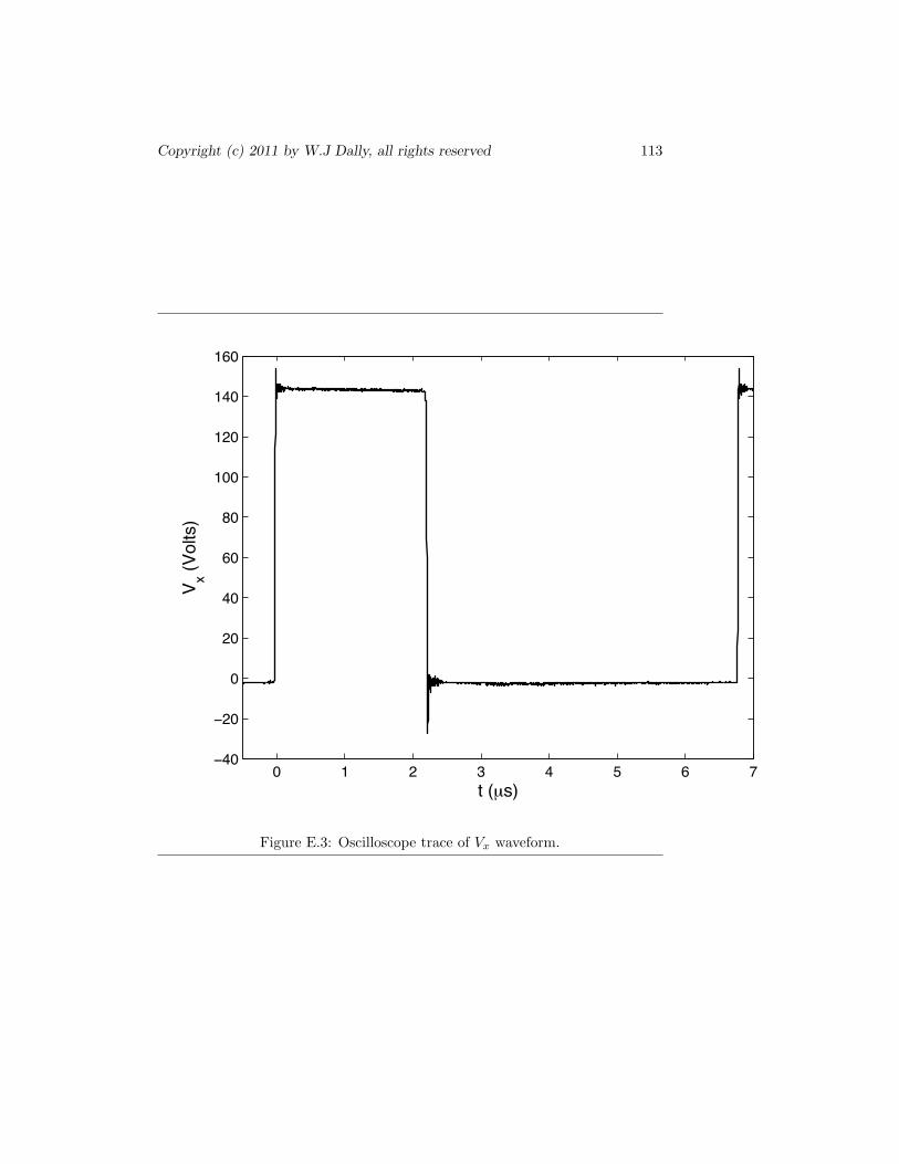
Copyright (c) 2011 by W.J Dally, all rights reserved 113
0 1 2 3 4 5 6 740
20
0
20
40
60
80
100
120
140
160
V x (Vol
ts)
t (µs)
Figure E.3: Oscilloscope trace of Vx waveform.

114 Green Electronics Class Notes
0 10 20 30 40 50 60 70 80
0
20
40
60
80
100
120
140
160
V x (Vol
ts)
t (ns)
Figure E.4: Close-up of rising edge of Vx. Rise time is 15ns and overshoot is14V.
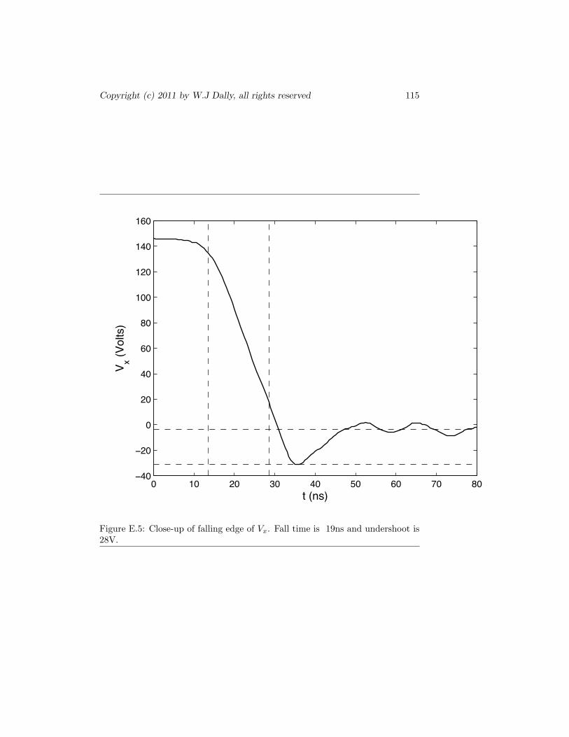
Copyright (c) 2011 by W.J Dally, all rights reserved 115
0 10 20 30 40 50 60 70 8040
20
0
20
40
60
80
100
120
140
160
V x (Vol
ts)
t (ns)
Figure E.5: Close-up of falling edge of Vx. Fall time is 19ns and undershoot is28V.

116 Green Electronics Class Notes
E.1.2 Input Snubber
E.1.3 Overlap Current

Appendix F
Motor and Battery Cart
contains motors with sensorsload48V of batteries with switch and fuse
117

118 Green Electronics Class Notes

Appendix G
Project Ideas
Power-Factor Correcting Input Circuit:
Inverter:
Battery Management System:
Battery State Indicator:
High-Efficiency Power Supply:
Intelligent Lighting:
Intelligent Appliance Control:
119

120 Green Electronics Class Notes

Appendix H
Circuit Theory
This appendix gives a quick overview of the basics of linear DC circuit the-ory. That is, circuits composed of independent current and voltage sources andresistors.
H.1 Voltage, Current, and Power
Electric circuits involve the movement of charged particles (electrons and holes)through conductors and components (such as resistors, capacitors, and induc-tors). We refer to the movement of charged particles as current which is mea-sured in Amperes or Amps which we abbreviate as A. One Ampere is a flow of1 Coulomb of charge every second.
If we move a charge carrier across an electric field, that carrier aquires po-tential energy - just as if we lift a mass through a gravitational field. We referto the potential of a particle as its voltage which is measured in Volts. A con-ductive node of a circuit has carriers that are all of the same potential which werefer to as the voltage of that node. We pick one node in a circuit arbitrarily tobe a reference of zero Volts — this is often called ground or GND.
Many people find an analogy to hydraulics helpful to understand currentand voltage. An electrical circuit is analgous to a hydraulic circuit — wherewater molecules replaces the charge carriers. The voltage of a node correspondsto the pressure in a water pipe. The current in a wire corresponds to the flowof water through a pipe — liters per second.
The power produced by a source is the product of the voltage across thesource times the current out of the source:
P = V I. (H.1)
If the net current flows into the positive terminal of a device, we refer to it asa load rather than a source. We tend to refer to power out of a source or into aload.
121
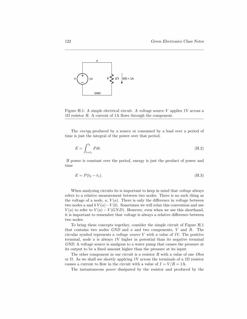
122 Green Electronics Class Notes
R
a
GND
+_V I(R) = 1A 1V 1
Figure H.1: A simple electrical circuit. A voltage source V applies 1V across a1Ω resistor R. A current of 1A flows through the component.
The energy produced by a source or consumed by a load over a period oftime is just the integral of the power over that period.
E =∫ t2
t=t1
Pdt. (H.2)
If power is constant over the period, energy is just the product of power andtime
E = P (t2 − t1). (H.3)
When analyzing circuits its is important to keep in mind that voltage alwaysrefers to a relative measurement between two nodes. There is no such thing asthe voltage of a node, a, V (a). There is only the difference in voltage betweentwo nodes a and b V (a)−V (b). Sometimes we will relax this convention and useV (a) to refer to V (a)− V (GND). However, even when we use this shorthand,it is important to remember that voltage is always a relative difference betweentwo nodes.
To bring these concepts together, consider the simple circuit of Figure H.1that contains two nodes GND and a and two components, V and R. Thecircular symbol represents a voltage source V with a value of 1V. The positiveterminal, node a is always 1V higher in potential than its negative terminalGND. A voltage source is analgous to a water pump that causes the pressure atits output to be a fixed amount higher than the pressure at its input.
The other component in our circuit is a resistor R with a value of one Ohmor Ω. As we shall see shortly applying 1V across the terminals of a 1Ω resistorcauses a current to flow in the circuit with a value of I = V/R = 1A.
The instantaneous power dissipated by the resistor and produced by the
Copyright (c) 2011 by W.J Dally, all rights reserved 123
source is given by:
P = V I. (H.4)
This is analagous to water flowing down a hill returning its potential energyas kinetic — and ultimately thermal — energy. A component dissipates powerif current flows into its more positive terminal — like the resistor in Figure H.1and it generates power if current flows out of its more positive terminal — likethe voltage source in Figure H.1.
H.2 Resistors and Ohm’s Law
A resistor, like the one in our simple circuit, is a passive element that, as itsname implies, resists current flow. Giving a current that is proportional to thevoltage applied across its terminals. The flow of current through the resistor isgoverned by Ohms Law:
V = IR, (H.5)
or equivalently:
I = V/R. (H.6)
The constant of proportionality that relates voltage and current here is calledresistance and has units of Ohms, abbreviated Ω.
Figure H.2 shows photographs of a few example resistors. Most resistorstoday are surface-mount (SMT) resistors like those shown in Figure H.2(a).These small rectalinear solids are soldered directly to the surface of a printedcircuit board. Each resistor is labeled with its resistance in scientific notationwith the “E” omitted. For example, the resistors labeled 222 have a resistanceof 22E2 or 2,200Ωor 2.2kΩ.
SMT resistors are described by their resistance and their size, which is spec-ified by their length and width in hundredths of an inch. The resistors inFigure H.2(a) are 0805 resistors which are 0.08 × 0.05 inch (2.0 × 1.3 mm) andhave a power rating of 0.1W. Resistors as small as 01005 (0.01 × 0.005 inch)with a power rating of 1/32 W are widely used.
Older systems use through-hole resistors like the 1/4 Watt resistor shown inFigure H.2(b). These resistors are inserted through holes in a printed-circuitboard and soldered in place. Through hole components are often used for small-quantity prototypes because they are easier to assemble by hand and reworkthan SMT components. SMT components, however, are preferred for high-volume assemblies because they are less expensive to assemble with automatedmachinery, require less board area, and don’t require holes to be drilled andplated.
Small through-hole resistors are labeled with their resistance value using thecolor code shown in Table H.1. For example, the resistor in Figure H.2(b) has
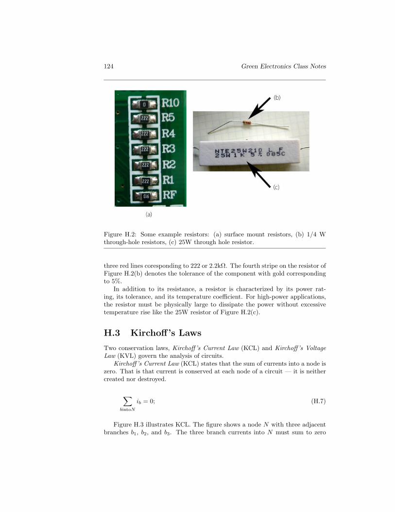
124 Green Electronics Class Notes
Figure H.2: Some example resistors: (a) surface mount resistors, (b) 1/4 Wthrough-hole resistors, (c) 25W through hole resistor.
three red lines coresponding to 222 or 2.2kΩ. The fourth stripe on the resistor ofFigure H.2(b) denotes the tolerance of the component with gold correspondingto 5%.
In addition to its resistance, a resistor is characterized by its power rat-ing, its tolerance, and its temperature coefficient. For high-power applications,the resistor must be physically large to dissipate the power without excessivetemperature rise like the 25W resistor of Figure H.2(c).
H.3 Kirchoff’s Laws
Two conservation laws, Kirchoff’s Current Law (KCL) and Kirchoff’s VoltageLaw (KVL) govern the analysis of circuits.
Kirchoff’s Current Law (KCL) states that the sum of currents into a node iszero. That is that current is conserved at each node of a circuit — it is neithercreated nor destroyed.
∑bintoN
ib = 0; (H.7)
Figure H.3 illustrates KCL. The figure shows a node N with three adjacentbranches b1, b2, and b3. The three branch currents into N must sum to zero

Copyright (c) 2011 by W.J Dally, all rights reserved 125
Color ValueBlack 0Brown 1Red 2Orange 3Yellow 4Green 5Blue 6Violet 7Gray 8White 9Gold -1Silver -2
Table H.1: Numeric color code used for labeling electronic components.
NIb1 Ib3
Ib2
b1
b2
b3
Figure H.3: Kirchoff’s current law (KCL). The three currents into node N mustsum to zero, Ib1 + Ib2 + Ib3 = 0.
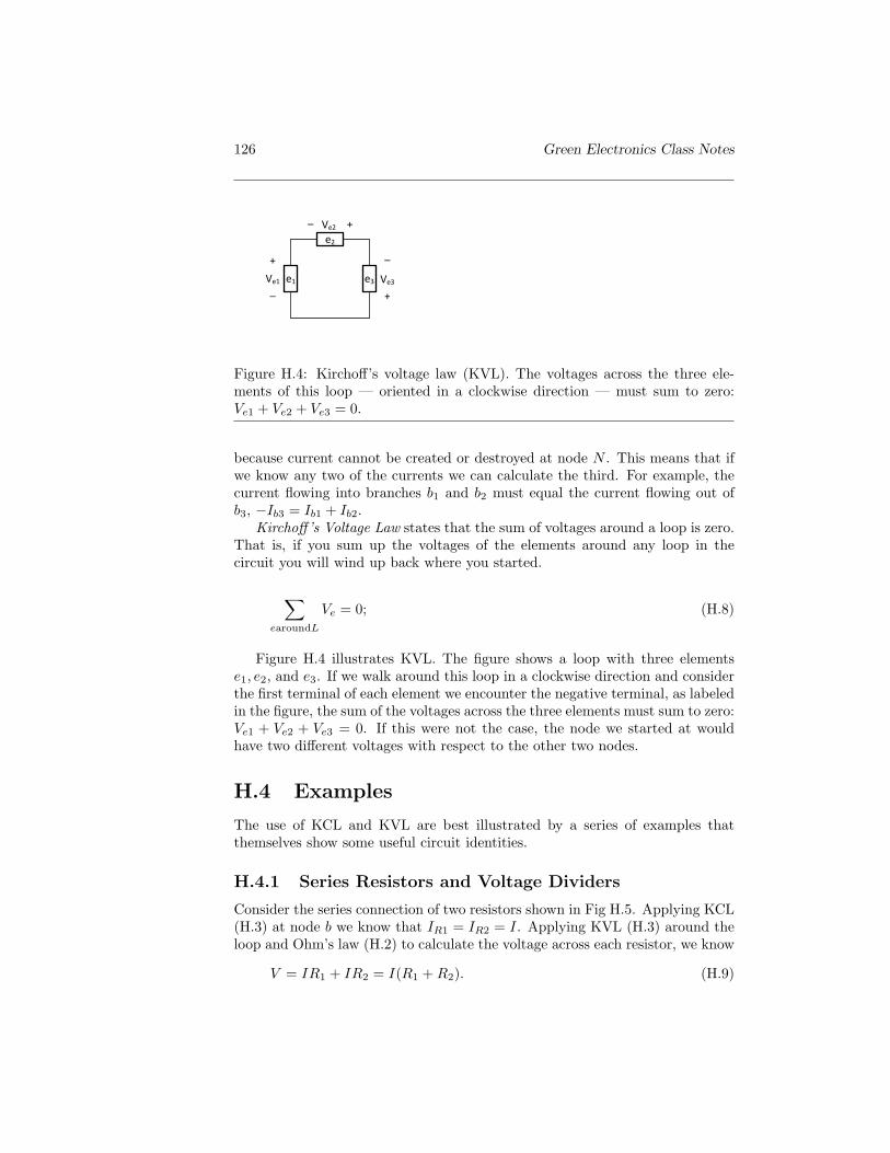
126 Green Electronics Class Notes
e2
e1 e3
+
_Ve1
_
+
Ve3
+_ Ve2
Figure H.4: Kirchoff’s voltage law (KVL). The voltages across the three ele-ments of this loop — oriented in a clockwise direction — must sum to zero:Ve1 + Ve2 + Ve3 = 0.
because current cannot be created or destroyed at node N . This means that ifwe know any two of the currents we can calculate the third. For example, thecurrent flowing into branches b1 and b2 must equal the current flowing out ofb3, −Ib3 = Ib1 + Ib2.
Kirchoff’s Voltage Law states that the sum of voltages around a loop is zero.That is, if you sum up the voltages of the elements around any loop in thecircuit you will wind up back where you started.
∑earoundL
Ve = 0; (H.8)
Figure H.4 illustrates KVL. The figure shows a loop with three elementse1, e2, and e3. If we walk around this loop in a clockwise direction and considerthe first terminal of each element we encounter the negative terminal, as labeledin the figure, the sum of the voltages across the three elements must sum to zero:Ve1 + Ve2 + Ve3 = 0. If this were not the case, the node we started at wouldhave two different voltages with respect to the other two nodes.
H.4 Examples
The use of KCL and KVL are best illustrated by a series of examples thatthemselves show some useful circuit identities.
H.4.1 Series Resistors and Voltage Dividers
Consider the series connection of two resistors shown in Fig H.5. Applying KCL(H.3) at node b we know that IR1 = IR2 = I. Applying KVL (H.3) around theloop and Ohm’s law (H.2) to calculate the voltage across each resistor, we know
V = IR1 + IR2 = I(R1 + R2). (H.9)
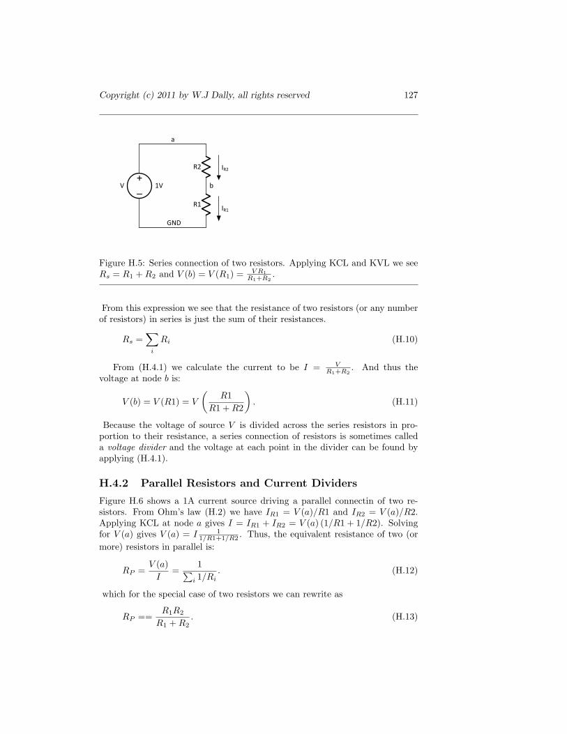
Copyright (c) 2011 by W.J Dally, all rights reserved 127
R1
a
GND
+_V
IR1
1V
R2
b
IR2
Figure H.5: Series connection of two resistors. Applying KCL and KVL we seeRs = R1 + R2 and V (b) = V (R1) = V R1
R1+R2.
From this expression we see that the resistance of two resistors (or any numberof resistors) in series is just the sum of their resistances.
Rs =∑
i
Ri (H.10)
From (H.4.1) we calculate the current to be I = VR1+R2
. And thus thevoltage at node b is:
V (b) = V (R1) = V
(R1
R1 + R2
). (H.11)
Because the voltage of source V is divided across the series resistors in pro-portion to their resistance, a series connection of resistors is sometimes calleda voltage divider and the voltage at each point in the divider can be found byapplying (H.4.1).
H.4.2 Parallel Resistors and Current Dividers
Figure H.6 shows a 1A current source driving a parallel connectin of two re-sistors. From Ohm’s law (H.2) we have IR1 = V (a)/R1 and IR2 = V (a)/R2.Applying KCL at node a gives I = IR1 + IR2 = V (a) (1/R1 + 1/R2). Solvingfor V (a) gives V (a) = I 1
1/R1+1/R2 . Thus, the equivalent resistance of two (ormore) resistors in parallel is:
RP =V (a)
I=
1∑i 1/Ri
. (H.12)
which for the special case of two resistors we can rewrite as
RP ==R1R2
R1 + R2. (H.13)

128 Green Electronics Class Notes
R1
a
GND
I IR11A R2 IR2
I
Figure H.6: Parallel connection of two resistors. Applying KVL and KVL wesee RP = 1
1/R1+1/R2 = R1R2R1+R2 and I(R1) = I/R1
1/R1+1/R2 = IR2R1+R2
.
The resistors in parallel act as a current divider with the amount of currentI flowing in resistor Ri being proportional to 1/Ri.
IR1 = I
(1/R1
1/R1 + 1/R2
)= I
(R2
R1 + R2
). (H.14)
The reciprocal of resistance is called conductance, Gi = 1/Ri. Rewriting(H.4.2) in terms of conductance, we have
IR1 = I
(G1
G1 + G2
). (H.15)
H.4.3 Combined Series Parallel Circuit
Consider the series-parallel circuit of Figure H.7(a). Suppose we need to solvefor the voltage at node b. We start by replacing the parallel combination of R2
and R3 with an equivalent resistor RP using (H.4.2) as shown in Figure H.7(b).Then applying (H.4.1) we have
V (b) = V
(RS
R1 + RS
), (H.16)
= V
(R2R3
R2+R3
R1 + R2R3R2+R3
), (H.17)
= V
(R2R3
R1R2 + R1R3 + R2R3
). (H.18)

Copyright (c) 2011 by W.J Dally, all rights reserved 129
R1
a
GND
+_V 1V
R2
b
R3
R1
a
GND
+_V 1V
RP=
b
(a) (b)
R2R3
R2 + R3
Figure H.7: A series-parallel resistor circuit.
Two-PortNetwork
+
_
V
I
V
I
ISC
VOC
Figure H.8: V-I characteristics. A two-port network can be characterized by itsV-I characteristic. If the network is linear this characteristic is a straight linewith intercepts at the network’s open-circuit voltage VOC and its short-circuitcurrent ISC .
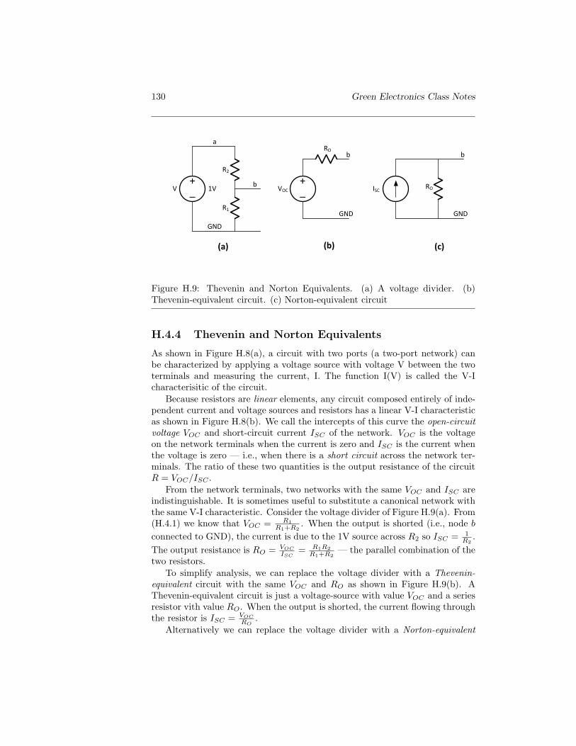
130 Green Electronics Class Notes
R1
a
GND
+_V 1V
R2
b +_VOC
RO
(a) (b)
ISC RO
b
GND
b
GND
(c)
Figure H.9: Thevenin and Norton Equivalents. (a) A voltage divider. (b)Thevenin-equivalent circuit. (c) Norton-equivalent circuit
H.4.4 Thevenin and Norton Equivalents
As shown in Figure H.8(a), a circuit with two ports (a two-port network) canbe characterized by applying a voltage source with voltage V between the twoterminals and measuring the current, I. The function I(V) is called the V-Icharacterisitic of the circuit.
Because resistors are linear elements, any circuit composed entirely of inde-pendent current and voltage sources and resistors has a linear V-I characteristicas shown in Figure H.8(b). We call the intercepts of this curve the open-circuitvoltage VOC and short-circuit current ISC of the network. VOC is the voltageon the network terminals when the current is zero and ISC is the current whenthe voltage is zero — i.e., when there is a short circuit across the network ter-minals. The ratio of these two quantities is the output resistance of the circuitR = VOC/ISC .
From the network terminals, two networks with the same VOC and ISC areindistinguishable. It is sometimes useful to substitute a canonical network withthe same V-I characteristic. Consider the voltage divider of Figure H.9(a). From(H.4.1) we know that VOC = R1
R1+R2. When the output is shorted (i.e., node b
connected to GND), the current is due to the 1V source across R2 so ISC = 1R2
.The output resistance is RO = VOC
ISC= R1R2
R1+R2— the parallel combination of the
two resistors.To simplify analysis, we can replace the voltage divider with a Thevenin-
equivalent circuit with the same VOC and RO as shown in Figure H.9(b). AThevenin-equivalent circuit is just a voltage-source with value VOC and a seriesresistor vith value RO. When the output is shorted, the current flowing throughthe resistor is ISC = VOC
RO.
Alternatively we can replace the voltage divider with a Norton-equivalent

Copyright (c) 2011 by W.J Dally, all rights reserved 131
circuit as shown in Figure H.9(c). Here a current source with value ISC isconnected in parallel with a resistor with value RO. When no output currentflows, all of the current from the source flows through the resistor generatingVOC = ISCRO.
H.5 Linearity and Superposition

132 Green Electronics Class Notes
Appendix I
Capacitors and RC Circuits
Green Electronic systems rely heavily on capacitors and inductors, circuit ele-ments that store energy so that we can convert it from one form to another. Inthis chapter we will explore the properties of capacitors and circuits composedof capacitors and resistors. In Appendix J we will visit inductors.
I.1 Capacitors
A capacitor is a two-terminal device that stores energy in an electric field.A schematic symbol for a capacitor is shown in ??. As current flows into acapacitor, the capacitor charges up, building up voltage across its two terminals.The capacitor can later be discharged releasing the stored energy.
At any point in time, the charge Q in the capacitor is proportional to thevoltage across the capacitor’s terminals.
q = Cv (I.1)
The constant here C is the capacitance. Differentiating Erefcap1 with respectto time gives us
dq
dt= C
dv
dt(I.2)
i = Cdv
dt(I.3)
(I.4)
Thus, we see that the current through a capacitor is proportional to the deriva-tive of the voltage across the capacitor.
Returning to our analogy to hydraulics, a capacitor is like a tank of water.As water flows into the tank the level in the tank, and hence the pressure at thebottom of the tank, increases. Similarly, as current flows into a capacitor thevoltage in the capacitor increases.
133
134 Green Electronics Class Notes
Figure I.1: RC Circuits: (a) a low-pass filter, (b) a high-pass filter
If we start with a discharged capacitor and charge it to V volts with a steady1A current, the capacitor voltage will increase linearly over the CV secondsrequired to complete the charge, so v(t) = t/C. At any point in time, thecharging power is P = iv = v = t/C. Thus, integrating over the CV secondsthe total charging energy, which is stored in the capacitor at the end of charging,is:
EC =∫ CV
0
t
Cdt =
12C
t2|CV0 =
CV 2
2. (I.5)
Capacitor circuits are particularly easy to analyze using Laplace transforms.Taking the transform of (I.1) gives:
i(s) = Csv(s). (I.6)
Thus, we can consider a capacitor as an impedance with value:
ZC =V (s)I(s)
=1
Cs. (I.7)
I.2 RC Circuits
We use KCL and KVL to analyze RC circuits in the same manner that we ana-lyzed purely resistive circuits. Consider the high-pass filter circuit of Figure ??.This is just a voltage divider with the bottom resistor replaced by a capacitor.From KCL we know that the current in the resistor is the same as the currentin the capacitor, thus we have
vi − vo
R= C
dvo
dt. (I.8)
We can solve (I.2) for specific waveforms vi(t). For example, for a unit step,vi(t) = u(t), we have
vo(t) = 1− exp
(t
RC
). (I.9)
This is a low-pass response with a time constant of τ = RC.As a second example, consider the
I.3 Impulse Response and Step Response
Appendix J
Inductors, LR, and LCCircuits
135

136 Green Electronics Class Notes
Appendix K
Operational Amplifiers
An operational amplifier or opamp is a three-terminal device that provides gain.That is, the power out of the amplifier is greater than the power into the am-plifier. We use opamps to construct a variety of signal conditioning circuits toamplify, level shift, and filter circuits. This appendix introduces the opamp,describes how to analyze opamp circuits, gives a number of example circuits,and discusses the limitations of real opamps.
K.1 Model
As shown in Figure K.1, an opamp can be modeled as a dependent voltagesource where the output voltage is proportional to the difference between thepositive and negative input voltages.
VO = A (VP − VN ) (K.1)
The gain A is assumed to be very large.An opamp is most often used with negative feedback from the output to the
negative input. Because the gain A is very large, as long as the output of theopamp remains in its operating region (i.e., it doesn’t peg at a power supply),the negative feedback will drive the negative input to the same voltage as thepositive input. Thus, when we analyze opamp circuits with negative feeback wecan, to first approximation, assume VN = VP .
With this assumption, analyzing an opamp circuit is a simple process. Wefirst compute the voltage on the positive input, VP . Then, we calculate whatoutput voltage VO is required to make VN = VP . We illustrate this analysismethod in the next section on several common opamp circuits.
K.2 OpAmp Circuits
Figure K.2(a) shows an opamp connected as a voltage follower. As the nameimplies, the output voltage follows in the input voltage VO = VI . The opamp
137

138 Green Electronics Class Notes
+_ VO = A(VP-VN)
VO
VP
VN
+
_
VP
VO
(a)
VN
(b)
Figure K.1: An opamp can be modeled as a dependent voltage source. Theoutput voltage is equal to a gain A times the difference in input voltages, VO =A (VP − VN ): (a) schematic symbol, (b) model.
+
_
VI
VO
(a)
+
_
VP
VO
VI
(b)
Ri Rf
+
_
VO
VINRi Rf
Ri RfVIP
(c)
Figure K.2: Common opamp circuits: (a) voltage follower, (b) inverting andnon-inverting amplifier, (c) differential amplifer.

Copyright (c) 2011 by W.J Dally, all rights reserved 139
provides isolation and gives a low impedance drive. It is used for example toprovide a low-impedance copy of a voltage generated by a high-resistance voltagedivider (as in Figure 2.2).
The analysis of this circuit using our two-step procedure is trivial. Thevoltage on the positive input is VP = VI . Assuming VN = VP , the outputvoltage required is VO = VP = VI .
Figure K.2(b) shows an opamp connected as an inverting or non-invertingamplifier. From input VI this is an inverting amplifier while from input VP it isa non-inverting amplifer.
To analyze this circuit lets first consider the case where VP = 0, i.e., thepositive input is connected to ground. In this case our assumption that VN = VP
makes VN a virtual ground. Thus, the current in Ri flowing toward the inputis I(Ri) = − VI
Ri. Because no current flows into the opamp input, by KCL, all
of this current continues on into Rf giving V (Rf ) = I(Ri)Rf = −VIRf
Ri. With
VN = 0 this is also the output voltage:
VO = −VIRf
Ri. (K.2)
This circuit gives amplifies the input with a gain of −Rf
Ri.
Now consider the case where VP is non-zero and VI is zero. Assumign VN =VP , we have I(Ri) = VP
Rigiving a voltage across Rf of V (Rf ) = VP
Rf
Ri. This is
summed with the voltage VN = VP to give an output voltage of
VO = VN + V (Rf ) = VP + VPRf
Ri= VP
(1 +
Rf
Ri
). (K.3)
By superposition we can write the general expression for VO as:
VO = VP
(1 +
Rf
Ri
)− VI
Rf
Ri. (K.4)
Here the gain from the positive input is one more than the negation of the gainfrom the negative input.
In cases where we want to amplify a differential voltage, we would like thegains from the two inputs to be equal and opposite. The circuit shown inFigure K.2(c) accomplishes this by dividing VIP to give VP = VIP
Rf
Ri+Rf. Sub-
stituting this into (K.2) gives:
VO = (VPI − VNI)(
Rf
Ri
). (K.5)
Note that the common-mode rejection of this circuit depends on the matchingbetween the two pairs of resistors.
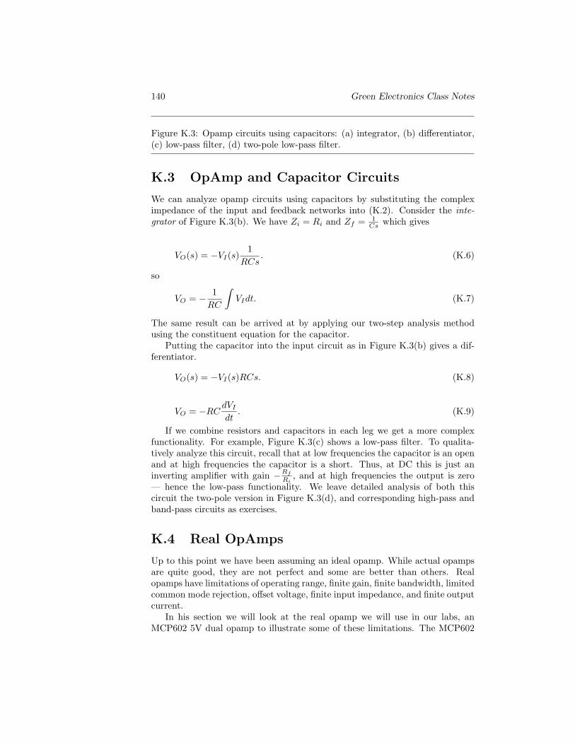
140 Green Electronics Class Notes
Figure K.3: Opamp circuits using capacitors: (a) integrator, (b) differentiator,(c) low-pass filter, (d) two-pole low-pass filter.
K.3 OpAmp and Capacitor Circuits
We can analyze opamp circuits using capacitors by substituting the compleximpedance of the input and feedback networks into (K.2). Consider the inte-grator of Figure K.3(b). We have Zi = Ri and Zf = 1
Cs which gives
VO(s) = −VI(s)1
RCs. (K.6)
so
VO = − 1RC
∫VIdt. (K.7)
The same result can be arrived at by applying our two-step analysis methodusing the constituent equation for the capacitor.
Putting the capacitor into the input circuit as in Figure K.3(b) gives a dif-ferentiator.
VO(s) = −VI(s)RCs. (K.8)
VO = −RCdVI
dt. (K.9)
If we combine resistors and capacitors in each leg we get a more complexfunctionality. For example, Figure K.3(c) shows a low-pass filter. To qualita-tively analyze this circuit, recall that at low frequencies the capacitor is an openand at high frequencies the capacitor is a short. Thus, at DC this is just aninverting amplifier with gain −Rf
Ri, and at high frequencies the output is zero
— hence the low-pass functionality. We leave detailed analysis of both thiscircuit the two-pole version in Figure K.3(d), and corresponding high-pass andband-pass circuits as exercises.
K.4 Real OpAmps
Up to this point we have been assuming an ideal opamp. While actual opampsare quite good, they are not perfect and some are better than others. Realopamps have limitations of operating range, finite gain, finite bandwidth, limitedcommon mode rejection, offset voltage, finite input impedance, and finite outputcurrent.
In his section we will look at the real opamp we will use in our labs, anMCP602 5V dual opamp to illustrate some of these limitations. The MCP602
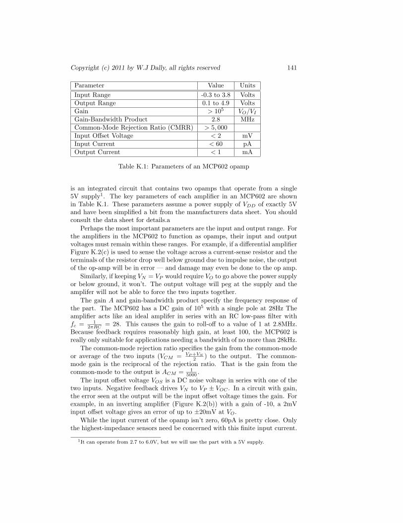
Copyright (c) 2011 by W.J Dally, all rights reserved 141
Parameter Value UnitsInput Range -0.3 to 3.8 VoltsOutput Range 0.1 to 4.9 VoltsGain > 105 VO/VI
Gain-Bandwidth Product 2.8 MHzCommon-Mode Rejection Ratio (CMRR) > 5, 000Input Offset Voltage < 2 mVInput Current < 60 pAOutput Current < 1 mA
Table K.1: Parameters of an MCP602 opamp
is an integrated circuit that contains two opamps that operate from a single5V supply1. The key parameters of each amplifier in an MCP602 are shownin Table K.1. These parameters assume a power supply of VDD of exactly 5Vand have been simplified a bit from the manufacturers data sheet. You shouldconsult the data sheet for details.a
Perhaps the most important parameters are the input and output range. Forthe amplifiers in the MCP602 to function as opamps, their input and outputvoltages must remain within these ranges. For example, if a differential amplifierFigure K.2(c) is used to sense the voltage across a current-sense resistor and theterminals of the resistor drop well below ground due to impulse noise, the outputof the op-amp will be in error — and damage may even be done to the op amp.
Similarly, if keeping VN = VP would require VO to go above the power supplyor below ground, it won’t. The output voltage will peg at the supply and theamplifer will not be able to force the two inputs together.
The gain A and gain-bandwidth product specify the frequency response ofthe part. The MCP602 has a DC gain of 105 with a single pole at 28Hz Theamplifier acts like an ideal amplifer in series with an RC low-pass filter withfc = 1
2πRC = 28. This causes the gain to roll-off to a value of 1 at 2.8MHz.Because feedback requires reasonably high gain, at least 100, the MCP602 isreally only suitable for applications needing a bandwidth of no more than 28kHz.
The common-mode rejection ratio specifies the gain from the common-modeor average of the two inputs (VCM = VP +VN
2 ) to the output. The common-mode gain is the reciprocal of the rejection ratio. That is the gain from thecommon-mode to the output is ACM = 1
5000 .The input offset voltage VOS is a DC noise voltage in series with one of the
two inputs. Negative feedback drives VN to VP ± VOC . In a circuit with gain,the error seen at the output will be the input offset voltage times the gain. Forexample, in an inverting amplifier (Figure K.2(b)) with a gain of -10, a 2mVinput offset voltage gives an error of up to ±20mV at VO.
While the input current of the opamp isn’t zero, 60pA is pretty close. Onlythe highest-impedance sensors need be concerned with this finite input current.
1It can operate from 2.7 to 6.0V, but we will use the part with a 5V supply.

142 Green Electronics Class Notes
On the other hand, the output drive is quite modest. If more than 1mA ofoutput current is needed, additional buffering is required.
K.5 Exercises
common mode rejectionlow pass analysistwo-pole low-pass analysishigh-passband-pass

Appendix L
Real Circuit Elements
L.1 Resistors
resistor - pretty close to ideal, power limit, tolerance
L.2 Inductors
inductor - series resistance, interwinding capacitance
L.3 Capacitors
capacitor - series inductance, esr types for different frequency bands and voltageselectrolytic polymer film (polycarbonate) ceramic
tolerances and standard values
L.4 Transformers
magnetizing and leakage inductancecore saturationseries resistance
L.5 Standard Values
L.6 Cost Model
a simple cost model for components
143

144 Green Electronics Class Notes

Appendix M
Switches
M.1 Metal-Oxide-Semiconductor Field Effect Tran-sistor (MOSFET)
MOSFETszero-th order model - on or off - when on has resistance Ron1st order model - turned on which charge - amount of charge determines
conductance Qth needed to start turning on Then conductance linearly goesfrom 0 to 1/Ron with next Qon Beyond that point
Gate is non-linear capacitorKey specifications are Vds max, Ids max, Ron, and tswFigure of merit is V 2/R which has dimensions of power.V /R per dollar is about 9E5 for 100V to 400V FETs and about 4E5 outside
this range.Table showing some typical power mosfets
M.2 Insulated-Gate Bipolar Transistors
IGBTsFigure of merit is P=VI All drop about 2V, so conduction power is 2I
Part No. VDSmax (V) IDSmax (A) RON (mΩ) Qg (nC)IRLB3036 60 195 2 91IRFB4332 250 60 29 99
Table M.1: Characteristics of selected power MOSFETs
145

146 Green Electronics Class Notes
M.3 Diodes
Switches to allow current to flow in only one direction. Called rectification.Simple control (none), but costs us a diode drop (from 0.5 to 2V) Function ofdiode often done today by MOSFET (synchronous rectification).
M.4 Silicon Controller Rectifiers (SCRs)
SCRs
M.5 Driver circuits
M.6 Isolation

Appendix N
Feedback Control
Many green electronic systems involve controlling a device to drive a key param-eter to a set point or to optimize some metric. For example, in our photovoltaiccontroller (Chapter ??) we control pulse width ta to drive the operating voltageof our solar cell array Vi to a set point Vt. This set point, in turn, is controlledto optimize power. As a second example, in our motor controller (Chapter ??)we control pulse width to drive motor torque to a set point.
In this chapter we show how the principles of feedback control can be appliedto build controllers of this type.
This chapter assumes a knowledge of Laplace transforms because their usegreatly simplifies the mathematics needed to describe these systems. If youare not familiar with Laplace transforms, you can use the results derived in acookbook manner without the need to understand their derivation.
N.1 Basic Principles
The principles of feedback control can be applied any time we need to control adevice via an input to drive an output to a desired setpoint. A basic feedback
Controller Plantx e a y
+
_
Figure N.1: A basic feedback control system. The The current output y issubtracted from the input set point x to produce an error signal e. A controlleruses the error signal to compute an input w to drive the plant to the desiredoutput.
147
148 Green Electronics Class Notes
control system is shown in Figure N.1. The device we are trying to control, calledthe plant, takes an input signal w and produces an output signal y. We use acontroller to generate the input signal based on an error signal, the differencebetween the desired set point and the current output, e = x− y.
There are many examples of feedback control in everyday life. The processof steering a car, for example, involves feedback control. In this case, the car isthe plant, the position (or angle) of the steering wheel is the input, w, and theposition of the car on the road is the output, y. The driver, as the controlleris mentally computing an error signal, e, by observing the difference betweenthe car’s position, y, and its desired position x, usually the center of the lane.Using this error signal, the driver determines a steering wheel angle w that willreturn the car to the desired position, x.
The car, as a plant, integrates the steering wheel position w to give theagngle, or direction of the car, and then integrates the angle of the car to giveits position on the road. Hence we have y(t) =
∫ ∫aw(t)dt2, where a is the gain
of the steering system (in units of ms2rad )
To generate an input w that drives the plant to the desired state, we willuse controllers that combine the error, its integral, and its derivative: integral
w(t) = pe(t) + q
∫e(t)dt + r
de(t)dt
. (N.1)
We refer to this as a proportional-integral-differential or PID controller. Theconstant’s p, q, and r are the proportional, integral, and differential gain respec-tively. The response of our overall system is determined by these three constantsalong with the characteristics of the plant. By setting p, q, and r appropriatelywe can get the plant output y(t) to track the input x(t), rapidly responding totransients in x but with minimum overshoot and no oscillation.
It is particularly important that we choose gain constants that give a stablesystem response, one where a bounded input gives a bounded output. Choosingthe constants incorrectly can give a system where a simple transient on theinput results in unbounded output oscillations, or where an input of a particularfrequency excites a resonance — giving an output of increasing magnitude.
Returning to our car example, if we use just a proportional controller, settingthe steering wheel position w equal to our distance from the center of the lane e,our car will oscillate back and forth across the centerline of the lane — and weare likely to get stopped and asked to take a sobriety test. To control the car in astable manner, we need to include a derivative term in our control law, reducingour steering input w proportion to the rate at which we are approaching thecenterline. In the sections below, we explain how to choose the proper valuesfor p, q, and r to give the desired response.
We often use subsets of the full PID controller. If all we need is proportionalcontrol, we use a P controller where q = r = 0. If r = 0 we have a PI controller,and if q = 0 we have a PD controller.
The rest of this section formulates a feedback control system using Laplacetransforms. If you are not familiar with Laplace transforms, you can skip to thebeginning of Section N.2.
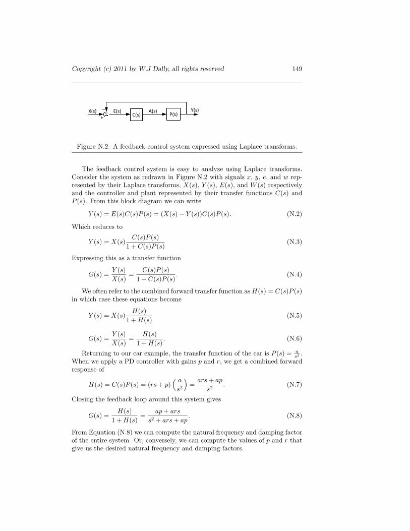
Copyright (c) 2011 by W.J Dally, all rights reserved 149
C(s) P(s)X(s) E(s) A(s) Y(s)
+
_
Figure N.2: A feedback control system expressed using Laplace transforms.
The feedback control system is easy to analyze using Laplace transforms.Consider the system as redrawn in Figure N.2 with signals x, y, e, and w rep-resented by their Laplace transforms, X(s), Y (s), E(s), and W (s) respectivelyand the controller and plant represented by their transfer functions C(s) andP (s). From this block diagram we can write
Y (s) = E(s)C(s)P (s) = (X(s)− Y (s))C(s)P (s). (N.2)
Which reduces to
Y (s) = X(s)C(s)P (s)
1 + C(s)P (s)(N.3)
Expressing this as a transfer function
G(s) =Y (s)X(s)
=C(s)P (s)
1 + C(s)P (s). (N.4)
We often refer to the combined forward transfer function as H(s) = C(s)P (s)in which case these equations become
Y (s) = X(s)H(s)
1 + H(s)(N.5)
G(s) =Y (s)X(s)
=H(s)
1 + H(s). (N.6)
Returning to our car example, the transfer function of the car is P (s) = as2 .
When we apply a PD controller with gains p and r, we get a combined forwardresponse of
H(s) = C(s)P (s) = (rs + p)( a
s2
)=
ars + ap
s2. (N.7)
Closing the feedback loop around this system gives
G(s) =H(s)
1 + H(s)=
ap + ars
s2 + ars + ap. (N.8)
From Equation (N.8) we can compute the natural frequency and damping factorof the entire system. Or, conversely, we can compute the values of p and r thatgive us the desired natural frequency and damping factors.

150 Green Electronics Class Notes
N.2 First Order System
A first-order system has a response that is determined by a first-order differentialequation. A typical first-order system is described by a single parameter, its timeconstant, τ , and it responds to a unit step on its input by following the inputwith an decaying exponental curve
y(t) = 1− exp(−t
τ
). (N.9)
As we shall see in the derivation below, we can improve the time constantof a first-order system by using a feedback control system with a PI controller.The resulting system is a second-order system. The gains of this controller pand q along with the original time constant τ determine the frequency ω andthe damping factor ζ of the resulting system as follows:
ω =√
aq (N.10)
where a = 1τ and
ζ =p + 12τω
=(
p + 12
)√a
q. (N.11)
Of course in designing controllers with these equations, it is important tokeep in mind that our controller has limited output range. For our photovoltaiccontroller of Chapter ??, for example, the pulse width ta is limited to a minimumof 0 (we can’t have a negative pulse width) and a maximum of tc (at most ourpulse can be high all the time). If we increase our gains in an attempt to makeour response time arbitrarily fast, we are likely to exceed the operating rangeof our controller. The controller will clip the input w to its range resulting innon-linear behavior. Clipping the input is not necessarily a bad thing, but itcauses the response to deviate from what is predicted by linear system analysis.
If you aren’t familiar with Laplace transforms, you can stop reading this sec-tion here. Equations (N.10) and (N.11) are all you need to design PI controllersfor first-order systems using a cookbook method. If you are curious how this isderived, read on.
Consider, for example, our motor control system. In this case, the motoris the plant, the input to the motor a is the pulse width (which determinesthe effective voltage seen by the motor), and the output y we are concernedwith is the motor’s torque, which is proportional to the current through themotor’s winding. For the special case where the motor is at rest, it is basicallyan inductor and if we ignore its series resistance we have
y = k
∫adt, (N.12)
where k is a constant that is proportional to VL . Taking the transform gives
P (s) =k
s(N.13)

Copyright (c) 2011 by W.J Dally, all rights reserved 151
and
Y (s) =kA(s)
s(N.14)
If we use a proportional control law, where the input is proportional to theerror a(t) = pe(t), substituting into (N.6) gives
G(s) =kp
s + kp=
a
s + a, (N.15)
where a = kp is the combined gain.If we apply a unit step, X(s) = 1
s to this system, the response is
Y (s) =a
s2 + as, (N.16)
which in the time domain gives
y(t) = 1− exp(−at). (N.17)
In this case, the feedback has converted the integrator into a first-ordersystem where the output follows the input with a time constant of τ = 1
a .The response of this system with a = 10 to a unit step function is shown inFigure N.3.
For a general first-order system where
P (s) =a
s + a. (N.18)
Applying a proportional controller with gain k gives
G(s) =ka
s + a(k + 1). (N.19)
The response to a unit step is
Y (s) =ka
s2 + a(k + 1)s. (N.20)
Which in the time domain is
G(s) =k
k + 1(1− exp(−a(k + 1)t)) . (N.21)
Here the feedback control has reduce the time constant by a factor of k + 1from τ = a−1 to τ = (a(k +1))−1. However, at the same time, the feedback hasreduced the overall gain from input to output from 1 to k
k+1 .If we want the output to exactly follow the input, a simple proportional
controller won’t do. One commoon approach is to add an integral term to ourcontrol equation. In this case
C(s) = p +q
s. (N.22)
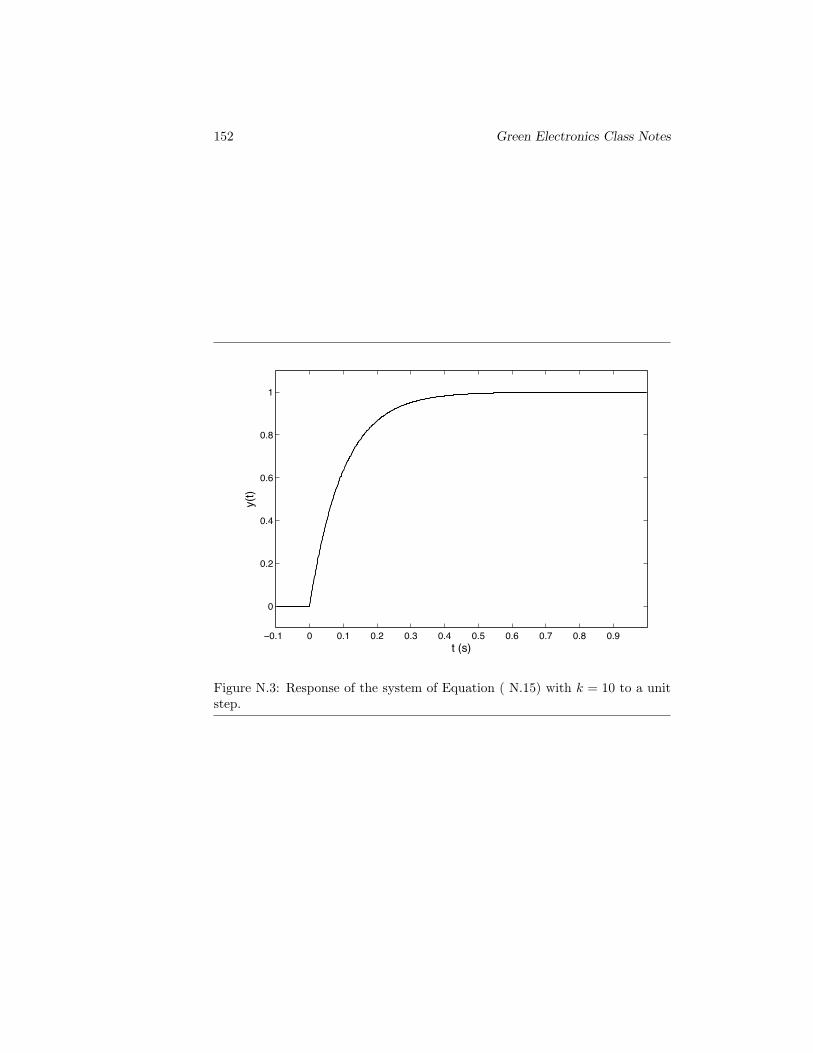
152 Green Electronics Class Notes
0.1 0 0.1 0.2 0.3 0.4 0.5 0.6 0.7 0.8 0.9
0
0.2
0.4
0.6
0.8
1
y(t)
t (s)
Figure N.3: Response of the system of Equation ( N.15) with k = 10 to a unitstep.
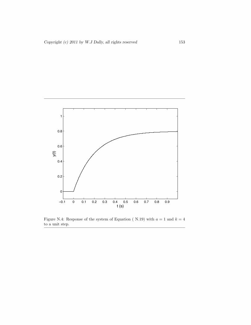
Copyright (c) 2011 by W.J Dally, all rights reserved 153
0.1 0 0.1 0.2 0.3 0.4 0.5 0.6 0.7 0.8 0.9
0
0.2
0.4
0.6
0.8
1
y(t)
t (s)
Figure N.4: Response of the system of Equation ( N.19) with a = 1 and k = 4to a unit step.
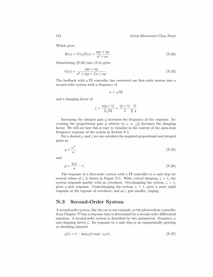
154 Green Electronics Class Notes
Which gives
H(s) = C(s)P (s) =aps + aq
s2 + as. (N.23)
Substituting (N.23) into (N.4) gives
G(s) =aps + aq
s2 + a(p + 1)s + aq. (N.24)
The feedback with a PI controller has converted our first-order system into asecond-order system with a frequency of
ω =√
aq
and a damping factor of
ζ =a(p + 1)2√
aq=
(p + 1)2
√a
q
.Increasing the integral gain q increases the frequency of the response. In-
creasing the proportional gain p relative to ω ∝ √q increases the damping
factor. We will see how this is easy to visualize in the context of the open-loopfrequency response of the system in Section N.5.
For a desired ω and ζ we can calculate the required proportional and integralgains as:
q =ω2
a. (N.25)
and
p =2ωζ
a− 1. (N.26)
The response of a first-order system with a PI controller to a unit step forseveral values of ζ is shown in Figure N.5. With critical damping, ζ = 1, thesystem responds quickly with no overshoot. Overdamping the system, ζ > 1,gives a slow response. Underdamping the system, ζ < 1, gives a more rapidresponse at the expense of overshoot, and as ζ gets smaller, ringing.
N.3 Second-Order System
A second-order system, like the car in our example, or the photovoltaic controllerfrom Chapter ?? has a response that is determined by a second-order differentialequation. A second-order system is described by two parameters: frequency ωand damping factor ζ. Its response to a unit step is an exponentially growingor shrinking sinusoid
y(t) = 1− sin(ωdt) exp(−ζωt), (N.27)
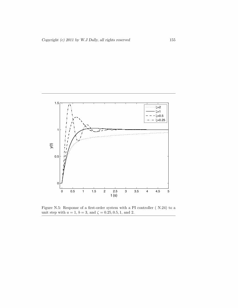
Copyright (c) 2011 by W.J Dally, all rights reserved 155
0 0.5 1 1.5 2 2.5 3 3.5 4 4.5 5
0
0.5
1
1.5
y(t)
t (s)
=2=1=0.5=0.25
Figure N.5: Response of a first-order system with a PI controller ( N.24) to aunit step with a = 1, b = 3, and ζ = 0.25, 0.5, 1, and 2.

156 Green Electronics Class Notes
where ωd = ω√
1− ζ2.
As we shall see in the derivation below, we can stabilize a second-ordersystem using a PD controller. The gains of this controller determine ω′ and ζ ′
of the feedback system as:
ω′ =√
ω2 + p (N.28)
ζ ′ =2ζω + r
2√
ω′. (N.29)
These equations make it clear that increasing the derivative gain r increases thedamping factor.
Again, if you are not familiar with Laplace transforms, you can stop readingthis section here and simply use Equations (N.28) and (N.29) as a cookbookmethod to design controllers for second-order systems. If you are curious abouttheir derivation, read on.
Let us consider first a second order system like our car that just integratesour input signal twice
P (s) =a
s2. (N.30)
From Equation (N.8) we know that applying a PD controller to this systemgives
G(s) =H(s)
1 + H(s)=
ap + ars
s2 + ars + ap. (N.31)
So we have ω =√
ap and ζ = ar2√
ap . Note the similarity of these terms to thosederived for first-order systems but with the roles of the gains shifted. The extra1s in the plant makes the proportional gain term act like an integral gain termon a first order-system and the derivative gain term act like the proportionalgain term on a first-order system.
For a more general second order system with a transfer function of
P (s) =b
s2 + as + b(N.32)
applying a PD controller gives
G(s) =brs + bp
s2 + (a + r)s + (b + p). (N.33)
So we have ω =√
b + p and ζ = a+r2√
b+p. Note also that the DC gain of the
system, is bpb+p .
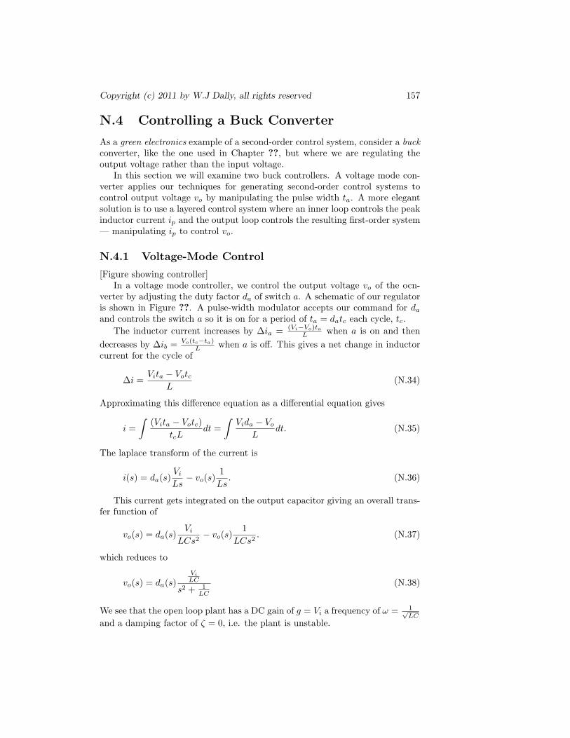
Copyright (c) 2011 by W.J Dally, all rights reserved 157
N.4 Controlling a Buck Converter
As a green electronics example of a second-order control system, consider a buckconverter, like the one used in Chapter ??, but where we are regulating theoutput voltage rather than the input voltage.
In this section we will examine two buck controllers. A voltage mode con-verter applies our techniques for generating second-order control systems tocontrol output voltage vo by manipulating the pulse width ta. A more elegantsolution is to use a layered control system where an inner loop controls the peakinductor current ip and the output loop controls the resulting first-order system— manipulating ip to control vo.
N.4.1 Voltage-Mode Control
[Figure showing controller]In a voltage mode controller, we control the output voltage vo of the ocn-
verter by adjusting the duty factor da of switch a. A schematic of our regulatoris shown in Figure ??. A pulse-width modulator accepts our command for da
and controls the switch a so it is on for a period of ta = datc each cycle, tc.The inductor current increases by ∆ia = (Vi−Vo)ta
L when a is on and thendecreases by ∆ib = Vo(tc−ta)
L when a is off. This gives a net change in inductorcurrent for the cycle of
∆i =Vita − Votc
L(N.34)
Approximating this difference equation as a differential equation gives
i =∫
(Vita − Votc)tcL
dt =∫
Vida − Vo
Ldt. (N.35)
The laplace transform of the current is
i(s) = da(s)Vi
Ls− vo(s)
1Ls
. (N.36)
This current gets integrated on the output capacitor giving an overall trans-fer function of
vo(s) = da(s)Vi
LCs2− vo(s)
1LCs2
. (N.37)
which reduces to
vo(s) = da(s)Vi
LC
s2 + 1LC
(N.38)
We see that the open loop plant has a DC gain of g = Vi a frequency of ω = 1√LC
and a damping factor of ζ = 0, i.e. the plant is unstable.
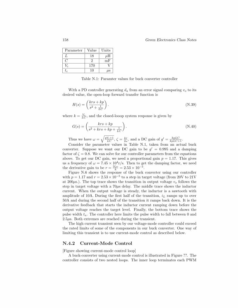
158 Green Electronics Class Notes
Parameter Value UnitsL 18 µHC 2 mFVi 170 Vtc 10 µs
Table N.1: Paramter values for buck converter controller
With a PD controller generating da from an error signal comparing vo to itsdesired value, the open-loop forward transfer function is
H(s) =(
krs + kp
s2 + 1LC
). (N.39)
where k = Vi
LC , and the closed-looop system response is given by
G(s) =(
krs + kp
s2 + krs + kp + 1LC
). (N.40)
Thus we have ω =√
pVi+1LC , ζ = kr
2ω , and a DC gain of g′ = kpLCkpLC+1 .
Consider the parameter values in Table N.1, taken from an actual buckconverter. Suppose we want our DC gain to be g′ = 0.995 and a dampingfactor of ζ = 0.8. We can solve for our controller parameters from the equationsabove. To get our DC gain, we need a proportional gain p = 1.17. This givesus a frequency of ω = 7.45 × 10⁴r/s. Then to get the damping factor, we needthe derivative gain to be r = 2ζω
k = 2.53× 10⁻⁵.Figure N.6 shows the response of the buck converter using our controller
with p = 1.17 and r = 2.53× 10⁻⁵ to a step in target voltage (from 20V to 21Vat 200µs.). The top trace shows the transition in output voltage vo follows thestep in target voltage with a 70µs delay. The middle trace shows the inductorcurrent. When the output voltage is steady, the inductor is a sawtooth withamplitude of 10A. During the first half of the transition, iL ramps up to over50A and during the second half of the transition it ramps back down. It is thederivative feedback that starts the inductor current ramping down before theoutput voltage reaches the target level. Finally, the bottom trace shows thepulse width ta. The controller here limits the pulse width to fall between 0 and2.5µs. Both extremes are reached during the transient.
The high current transient seen by our voltage-mode controller could exceedthe rated limits of some of the components in our buck converter. One way oflimiting this transient is to use current-mode control as described below.
N.4.2 Current-Mode Control
[Figure showing current-mode control loop]A buck-converter using current-mode control is illustrated in Figure ??. The
controller consists of two nested loops. The inner loop terminates each PWM
Copyright (c) 2011 by W.J Dally, all rights reserved 159
0 50 100 150 200 250 300 350 40019.5
20
20.5
21
V o (Vol
ts)
0 50 100 150 200 250 300 350 4000
20
40
60
I L (Am
ps)
0 50 100 150 200 250 300 350 4000
1
2
3
t a (µs)
t(µs)
Figure N.6: Response of our example PD feedback buck converter controller astep in the target voltage.
160 Green Electronics Class Notes
pulse when the inductor current reaches a target imax. The outer loop computesimax from the output voltage error e = vo − vt.
To simplify the analysis, assume the control variable sets average inductorcurrent i. Then our system is a simple first-order integrator:
vo =∫
i
Cdt, (N.41)
vo(s) =i(s)Cs
(N.42)
If we apply a PI controller to this first order system we have
H(s) =ps + q
Cs2. (N.43)
G(s) =pC s + q
C
s2 + pC s + q
C
. (N.44)
ω =√
q
C(N.45)
ζ =p
2Cω. (N.46)
If C = 2mF and we choose ω = 6.28 × 10⁴ (f = 10kHz) and ζ = 1 we getq = 7.89× 10⁶ and p = 251.
Figure N.7 shows the response of this current-mode buck controller to a stepin target voltage. To protect converter components, the controller is designedto limit the peak current to 30A. The top panel shows that the voltage rampssmoothly from 20 to 21V over 100µs, as fast as is possible given the peak currentlimitation. The second panel shows the target peak current ip computed by thePI controller which steps from 10A to 30A during the transition and then backto 10A. The actual inductor current waveform is shown in the third panel. Theinner loop controls switch a to make this current ramp up to ip each cycle in asawtooth waveform. The pulsewidths produced by the inner loop are shown inthe final panel.
Compared to the voltage-mode controller, the current mode controller pre-vents overstressing components with high current during transients, gives acrisper response, and is simpler to control and stabilize.
N.5 Frequency Response of Controllers
Considerable insight can be gained by looking at the frequency response of theforward transfer function, H(s), of a feedback control system (i.e., the transferfunction of the system with the feedback disconnected).
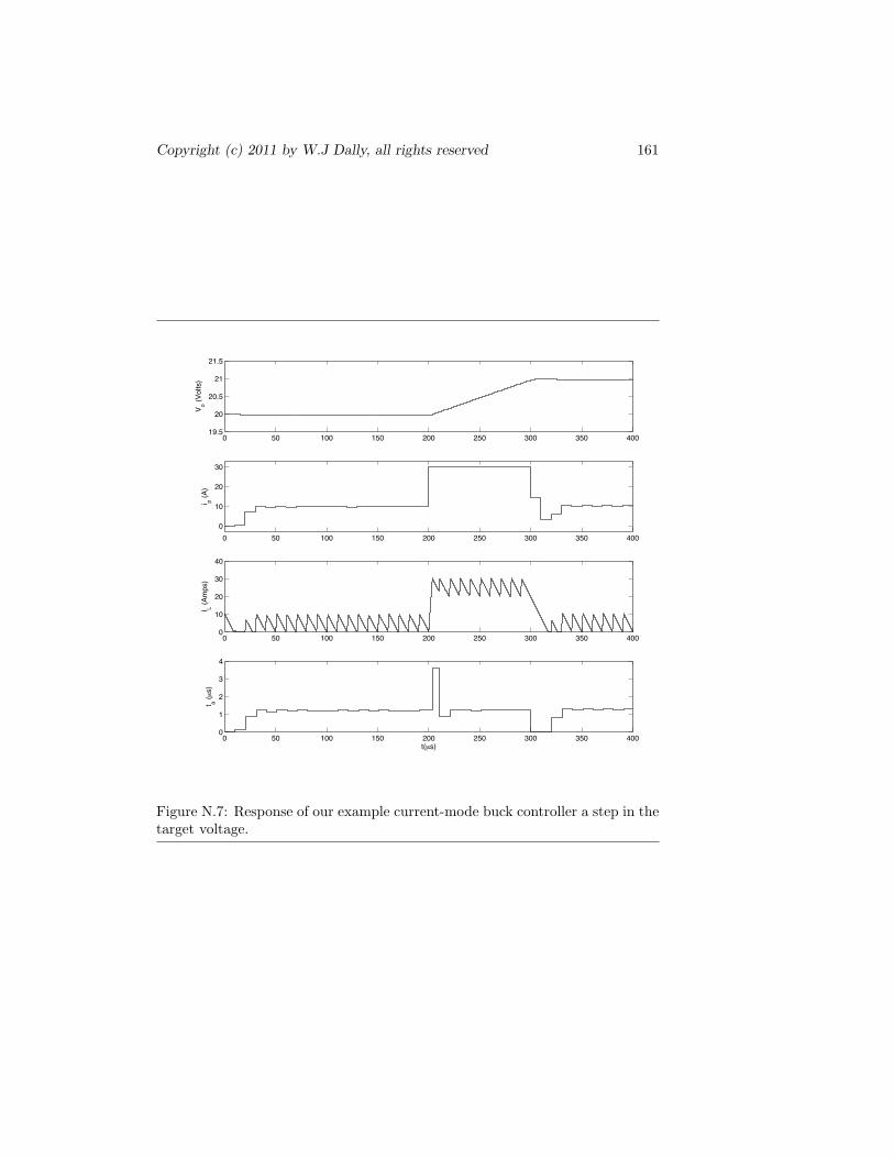
Copyright (c) 2011 by W.J Dally, all rights reserved 161
0 50 100 150 200 250 300 350 40019.5
20
20.5
21
21.5
V o (Vol
ts)
0 50 100 150 200 250 300 350 4000
10
20
30
i p (A)
0 50 100 150 200 250 300 350 4000
10
20
30
40
I L (Am
ps)
0 50 100 150 200 250 300 350 4000
1
2
3
4
t a (µs)
t(µs)
Figure N.7: Response of our example current-mode buck controller a step in thetarget voltage.
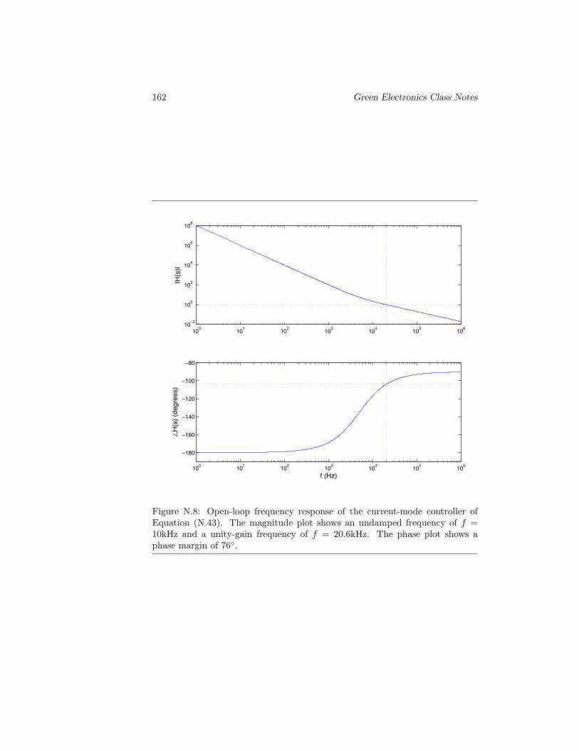
162 Green Electronics Class Notes
100 101 102 103 104 105 10610 2
100
102
104
106
108
|H(s
)|
100 101 102 103 104 105 106
180
160
140
120
100
80
H(s
) (de
gree
s)
f (Hz)
Figure N.8: Open-loop frequency response of the current-mode controller ofEquation (N.43). The magnitude plot shows an undamped frequency of f =10kHz and a unity-gain frequency of f = 20.6kHz. The phase plot shows aphase margin of 76.

Copyright (c) 2011 by W.J Dally, all rights reserved 163
For example, Figure N.8 shows the open-loop frequency response of of thebuck converter with current-mode control developed in Section N.4.2. Becauseof the s2 in the denominator (two poles at the origin), the response starts with aphase of -180 and the magnitude falls off at 20dB per decade. The PI controllerinserts a zero into the response at a frequency of f = q
2πp = 5kHz. This shiftsthe phase of the response to -90 (reaching -135 at 5kHz) at reduces the dropin magnitude to 10dB per decade.
The magnitude reaches unity-gain (shown by the dotted line) at f = 20.6kHz.The difference between the open-loop phase at this unity-gain frequency and -180 is called the phase margin of the system and determines the system stabil-ity. For our current-mode controller, the phase at unity gain is -104. This givesa phase margin of 180 − 104 = 76 which corresponds to a critically-dampedsystem (ζ = 1).
Without the stabilizing pole, an extrapolation of the 20db per decade linereaches unity gain at 10kHz, the value we chose for ω, the undamped frequency.
As a second example, Figure N.9 shows the frequency response of the forwardtransfer function of our voltage-mode controller of Section N.4.1. Here ourmagnitude response starts flat with a DC gain of pVi = 199 and a phase of 0.The tank circuit formed by the inductor and output capacitor introduce twopoles at the resonant frequency of f = 1
2π√
LC= 839Hz. This pair of poles
causes the phase to shift to -180 and causes the magnitude to peak and thenfall off at 20dB per decade. The magnitude reaches unity-gain at 20.1kHz.
The derivative feedback inserts a zero into the response at f = p2πr = 7.4kHz.
This zero shifts the phase back to -90 to stabilize the system. The phase marginat the unity-gain frequency of 20.1kHz is −110 corresponding to our choice ofζ = 0.8.
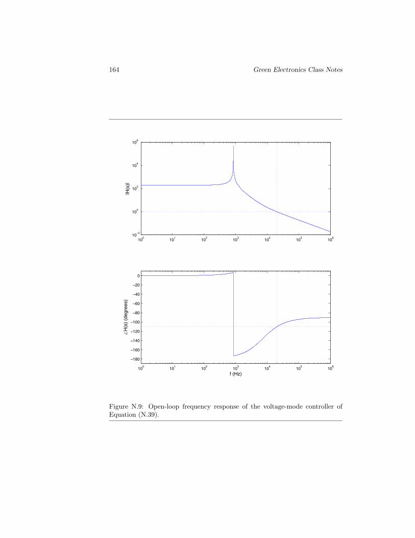
164 Green Electronics Class Notes
100 101 102 103 104 105 10610 2
100
102
104
106
|H(s
)|
100 101 102 103 104 105 106
180
160
140
120
100
80
60
40
20
0
H(s
) (de
gree
s)
f (Hz)
Figure N.9: Open-loop frequency response of the voltage-mode controller ofEquation (N.39).

Appendix O
SPICE Simulation
O.1 A Simple Example
O.2 Basic Circuit Elements
O.3 Subcircuits
O.4 Models and Libraries
O.5 Sources
O.6 Measurement Statements
O.7 A Detailed Example
165