Contents · Experiment #11(B) Inverting amplifier ... configuration, the base is common to both...
20
Transcript of Contents · Experiment #11(B) Inverting amplifier ... configuration, the base is common to both...

Contents
EXPERIMENT NO -9 TRANSITOR COMMON -BASE CONFIGURATION CHARACTERISTICS ............................. 3
EXPERIMENT NO -10. FET CHARACTERISTICS ............................................................................................... 8
Experiment # 11 Non-inverting amplifier .................................................................................................. 13
Experiment #11(B) Inverting amplifier ....................................................................................................... 15
Experiment # 12(a) Subtractor or Differential amplifier............................................................................. 17
Experiment # 12(B) Summing amplifier using Op Amp .............................................................................. 19
. ................................................................................................................................................................... 19
EXPERIMENT NO -9 TRANSITOR COMMON -BASE CONFIGURATION
CHARACTERISTICS
OBJECTIVE: 1.To observes and draw the input and output characteristics of a transistor
connected in common base configuration.
2. To find α of the given transistor and also its input and output Resistances.
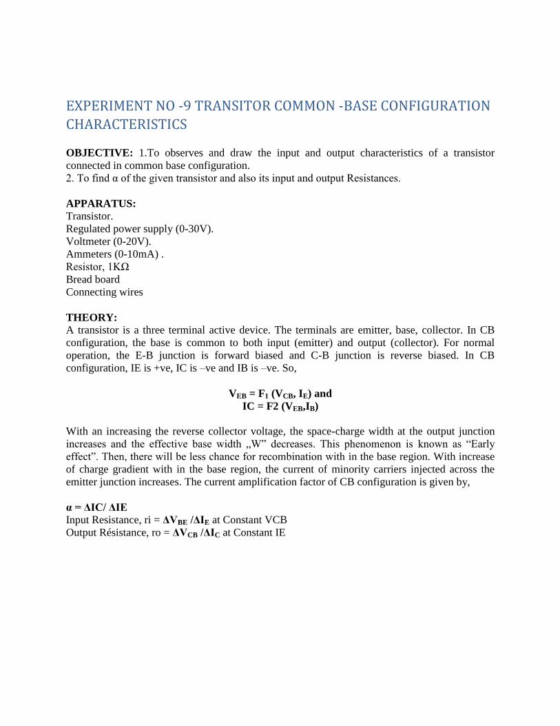
APPARATUS:
Transistor.
Regulated power supply (0-30V).
Voltmeter (0-20V).
Ammeters (0-10mA) .
Resistor, 1KΩ
Bread board
Connecting wires
THEORY:
A transistor is a three terminal active device. The terminals are emitter, base, collector. In CB
configuration, the base is common to both input (emitter) and output (collector). For normal
operation, the E-B junction is forward biased and C-B junction is reverse biased. In CB
configuration, IE is +ve, IC is –ve and IB is –ve. So,
VEB = F1 (VCB, IE) and
IC = F2 (VEB,IB)
With an increasing the reverse collector voltage, the space-charge width at the output junction
increases and the effective base width „W‟ decreases. This phenomenon is known as “Early
effect”. Then, there will be less chance for recombination with in the base region. With increase
of charge gradient with in the base region, the current of minority carriers injected across the
emitter junction increases. The current amplification factor of CB configuration is given by,
α = ΔIC/ ΔIE
Input Resistance, ri = ΔVBE /ΔIE at Constant VCB
Output Résistance, ro = ΔVCB /ΔIC at Constant IE
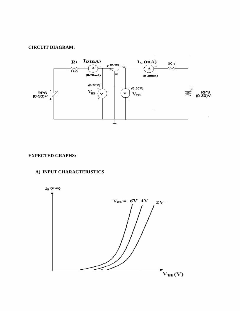
CIRCUIT DIAGRAM:
EXPECTED GRAPHS:
A) INPUT CHARACTERISTICS
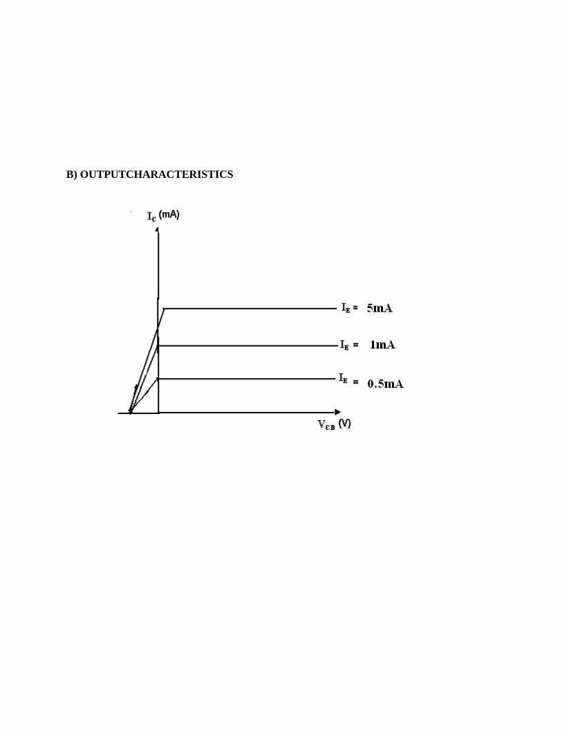
B) OUTPUTCHARACTERISTICS

OBSERVATIONS:
A) INPUT CHARACTERISTICS:
VEE(V) VCB=1V VCB=2V VCB=3V
VEB(V) IE(mA) VEB(V) IE(mA) VEB(V) IE(mA)
B) OUTPUT CHARACTERISTICS:
Vcc(V) IE=10mA IE=20mA IE=30mA
VCB(V) IC(mA) VCB(V) IC(mA) VCB(V) IC(mA)
PROCEDURE:
A) INPUT CHARACTERISTICS:
1. Connections are made as per the circuit diagram.
2. For plotting the input characteristics, the output voltage VCE is kept constant at 0V and for
different values of VEE ,note down the values of IE and VBE
3. Repeat the above step keeping VCB at 2V, 4V, and 6V and all the readings are tabulated.
4. A graph is drawn between VEB and IE for constant VCB.
B) OUTPUT CHARACTERISTICS:
1. Connections are made as per the circuit diagram.
2. For plotting the output characteristics, the input IE is kept constant at 0.5mA and for different
values of VCC, note down the values of IC and VCB.
3. Repeat the above step for the values of IE at 1mA, 5mA and all the readings are tabulated.
4. A graph is drawn between VCB and Ic for constant IE
RESULT: The Current gain of the Transistor in CB is ______ , the input Resistance is
_____ and the output Resistance is ______.
VIVA QUESTIONS:
1. What is the range of α for the transistor?
2. Draw the input and output characteristics of the transistor in CB configuration.
3. Identify various regions in output characteristics.
4. What is the relation between α and β?
5. What are the applications of CB configuration?
6. What are the input and output impedances of CB configuration?
7. Define α (alpha).
8. What is early effect?
9. Draw Circuit diagram of CB configuration for PNP transistor.
10. What is the power gain of CB configuration?
EXPERIMENT NO -10. FET CHARACTERISTICS
OBJECTIVE: a).To draw the drain and transfer characteristics of a given FET. b).To find the
drain resistance (rd.) amplification factor (μ) and Trans Conductance (gm) of the given FET.
APPARATUS:
FET
Regulated power supply (0-30V) -1No.
Voltmeter (0-20V) -2No.
Ammeter (0-20mA) -1No.
Bread board
Connecting wires
THEORY:
A FET is a three terminal device, in which current conduction is by majority carriers only. The
flow of current is controlled by means of an Electric field. The three terminals of FET are Gate,
Drain and Source. It is having the characteristics of high input impedance and less noise, the
Gate to Source junction of the FETs always reverse biased. In response to small applied voltage
from drain to source, the n-type bar acts as sample resistor, and the drain current increases
linearly with VDS. With increase in ID the ohmic voltage drop between the source and the channel
region reverse biases the junction and the conducting position of the channel begins to remain
constant. The VDS at this instant is called “pinch of voltage”. If the gate to source voltage (VGS)
is applied in the direction to provide additional reverse bias, the pinch off voltage ill is decreased.
In amplifier application, the FET is always used in the region beyond the pinch-off.
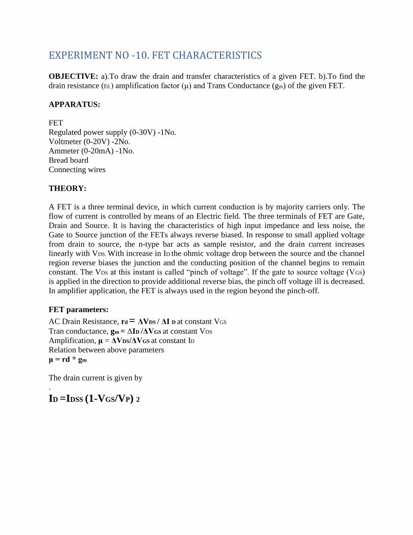
FET parameters:
AC Drain Resistance, rd = ΔVDS / ΔI D at constant VGS
Tran conductance, gm = ΔID /ΔVGS at constant VDS
Amplification, μ = ΔVDS/ΔVGS at constant ID
Relation between above parameters
μ = rd * gm
The drain current is given by
.
ID =IDSS (1-VGS/VP) 2
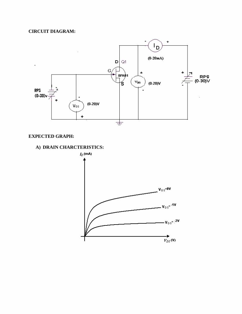
CIRCUIT DIAGRAM:
EXPECTED GRAPH:
A) DRAIN CHARCTERISTICS:
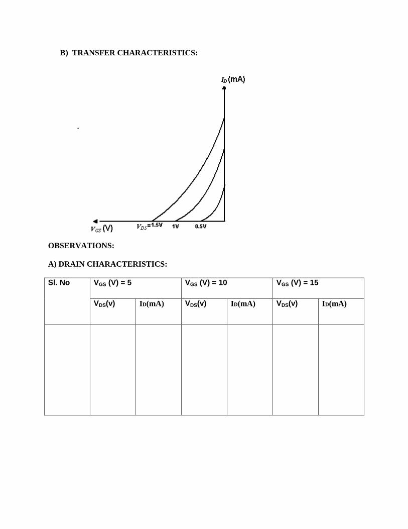
B) TRANSFER CHARACTERISTICS:
OBSERVATIONS:
A) DRAIN CHARACTERISTICS:
Sl. No VGS (V) = 5 VGS (V) = 10 VGS (V) = 15
VDS(v) ID(mA) VDS(v) ID(mA) VDS(v) ID(mA)
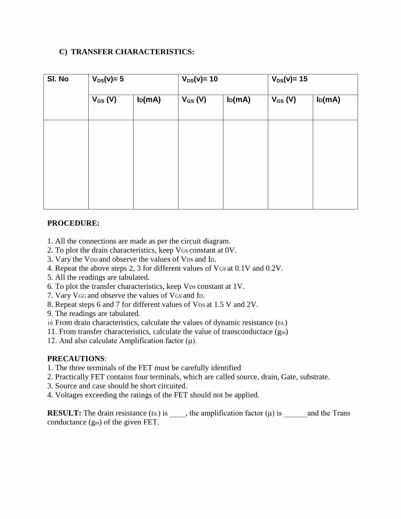
C) TRANSFER CHARACTERISTICS:
Sl. No VDS(v)= 5 VDS(v)= 10 VDS(v)= 15
VGS (V) ID(mA) VGS (V) ID(mA) VGS (V) ID(mA)
PROCEDURE:
1. All the connections are made as per the circuit diagram.
2. To plot the drain characteristics, keep VGS constant at 0V.
3. Vary the VDD and observe the values of VDS and ID.
4. Repeat the above steps 2, 3 for different values of VGS at 0.1V and 0.2V.
5. All the readings are tabulated.
6. To plot the transfer characteristics, keep VDS constant at 1V.
7. Vary VGG and observe the values of VGS and ID.
8. Repeat steps 6 and 7 for different values of VDS at 1.5 V and 2V.
9. The readings are tabulated.
10. From drain characteristics, calculate the values of dynamic resistance (rd.)
11. From transfer characteristics, calculate the value of transconductace (gm)
12. And also calculate Amplification factor (μ).
PRECAUTIONS:
1. The three terminals of the FET must be carefully identified
2. Practically FET contains four terminals, which are called source, drain, Gate, substrate.
3. Source and case should be short circuited.
4. Voltages exceeding the ratings of the FET should not be applied.
RESULT: The drain resistance (rd.) is ____, the amplification factor (μ) is ______and the Trans
conductance (gm) of the given FET.

VIVA QUESTIONS:
1. What are the advantages of FET?
2. What is the difference between FET and BJT?
3. Explain different regions of V-I characteristics of FET.
4. What are the applications of FET?
5. What are the types of FET?
Experiment # 11 Non-inverting amplifier
Objective: To understand the behavior of opamp in the case of using inverting & non inverting
pins .
Theory:
The input signal is applied to the non-inverting (+) input. The output is applied back to the
inverting (-) input through the feedback circuit (closed loop) formed by the input resistor R1
and the feedback resistor Rf. This creates –ve feedback as follows. Resistors R1 and Rf form a
voltage-divider circuit, which reduces VO and connects the reduced voltage Vf to the inverting
input. The feedback is expressed as
The difference of the input voltage, Vin and the feedback voltage, Vf is the differential input of
the opamp. This differential voltage is amplified by the gain of the op-amp and produces an
output voltage expressed as
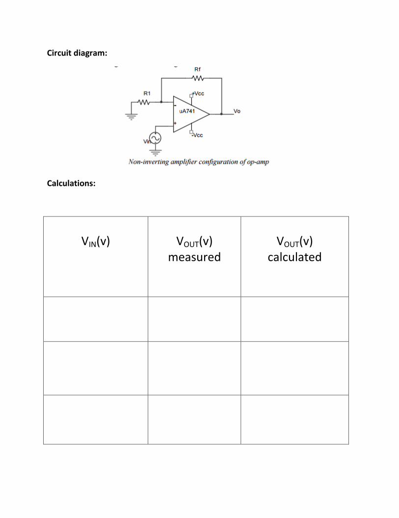
Circuit diagram:
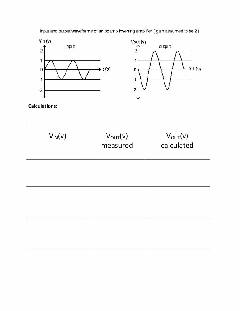
Calculations:
VIN(v)
VOUT(v)
measured
VOUT(v)
calculated
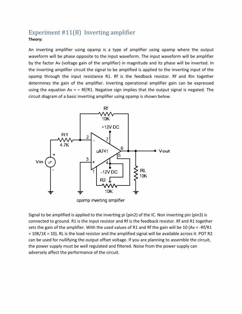
Experiment #11(B) Inverting amplifier Theory:
An inverting amplifier using opamp is a type of amplifier using opamp where the output
waveform will be phase opposite to the input waveform. The input waveform will be amplifier
by the factor Av (voltage gain of the amplifier) in magnitude and its phase will be inverted. In
the inverting amplifier circuit the signal to be amplified is applied to the inverting input of the
opamp through the input resistance R1. Rf is the feedback resistor. Rf and Rin together
determines the gain of the amplifier. Inverting operational amplifier gain can be expressed
using the equation Av = – Rf/R1. Negative sign implies that the output signal is negated. The
circuit diagram of a basic inverting amplifier using opamp is shown below.
Signal to be amplified is applied to the inverting pi (pin2) of the IC. Non inverting pin (pin3) is
connected to ground. R1 is the input resistor and Rf is the feedback resistor. Rf and R1 together
sets the gain of the amplifier. With the used values of R1 and Rf the gain will be 10 (Av = -Rf/R1
= 10K/1K = 10). RL is the load resistor and the amplified signal will be available across it. POT R2
can be used for nullifying the output offset voltage. If you are planning to assemble the circuit,
the power supply must be well regulated and filtered. Noise from the power supply can
adversely affect the performance of the circuit.
Calculations:
VIN(v)
VOUT(v)
measured
VOUT(v)
calculated
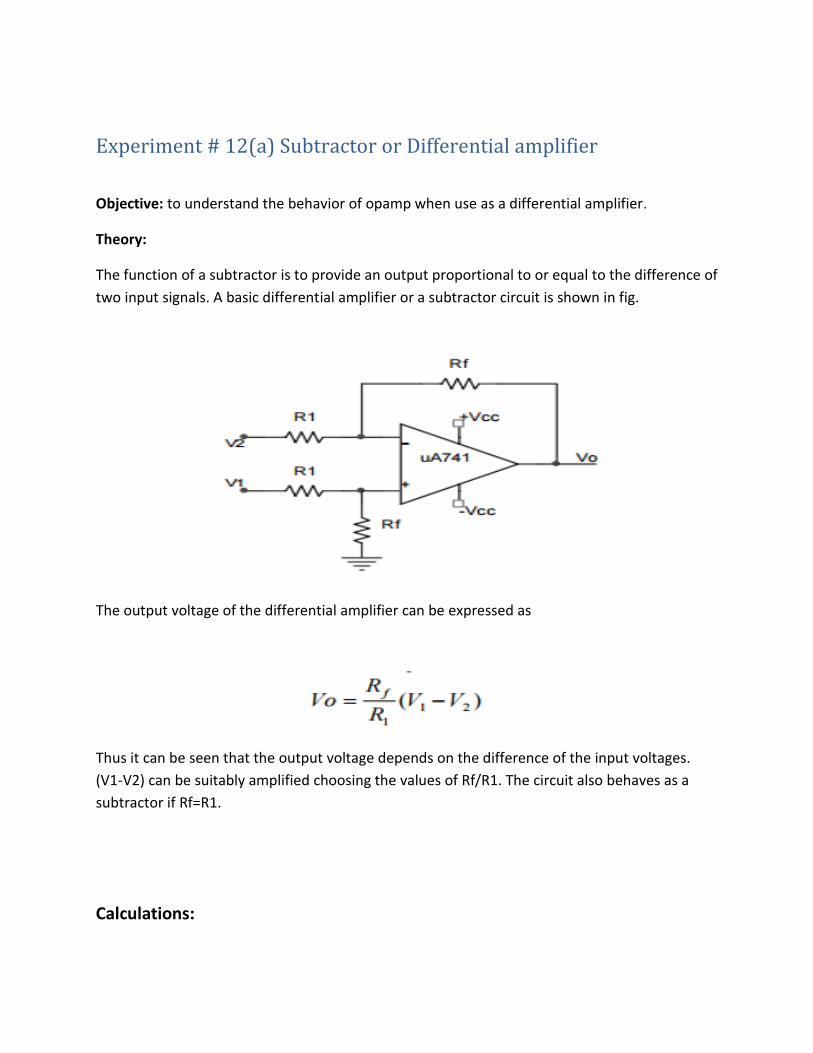
Experiment # 12(a) Subtractor or Differential amplifier
Objective: to understand the behavior of opamp when use as a differential amplifier.
Theory:
The function of a subtractor is to provide an output proportional to or equal to the difference of
two input signals. A basic differential amplifier or a subtractor circuit is shown in fig.
The output voltage of the differential amplifier can be expressed as
Thus it can be seen that the output voltage depends on the difference of the input voltages.
(V1-V2) can be suitably amplified choosing the values of Rf/R1. The circuit also behaves as a
subtractor if Rf=R1.
Calculations:

VIN1(v)
VIN2(v)
VOUT(v)
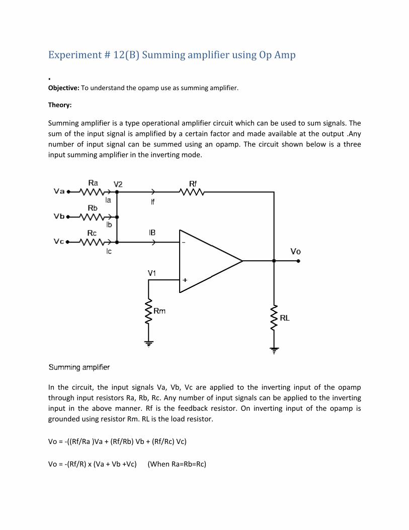
Experiment # 12(B) Summing amplifier using Op Amp
. Objective: To understand the opamp use as summing amplifier.
Theory:
Summing amplifier is a type operational amplifier circuit which can be used to sum signals. The
sum of the input signal is amplified by a certain factor and made available at the output .Any
number of input signal can be summed using an opamp. The circuit shown below is a three
input summing amplifier in the inverting mode.
In the circuit, the input signals Va, Vb, Vc are applied to the inverting input of the opamp
through input resistors Ra, Rb, Rc. Any number of input signals can be applied to the inverting
input in the above manner. Rf is the feedback resistor. On inverting input of the opamp is
grounded using resistor Rm. RL is the load resistor.
Vo = -((Rf/Ra )Va + (Rf/Rb) Vb + (Rf/Rc) Vc)
Vo = -(Rf/R) x (Va + Vb +Vc) (When Ra=Rb=Rc)
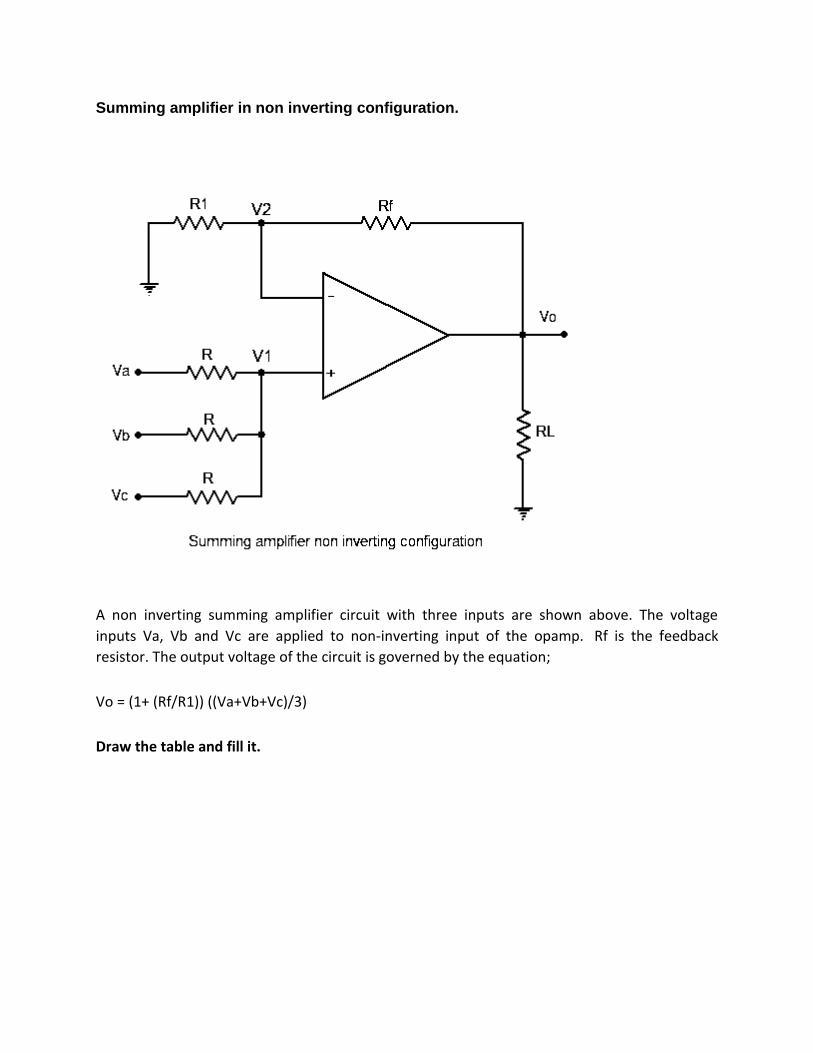
Summing amplifier in non inverting configuration.
A non inverting summing amplifier circuit with three inputs are shown above. The voltage
inputs Va, Vb and Vc are applied to non-inverting input of the opamp. Rf is the feedback
resistor. The output voltage of the circuit is governed by the equation;
Vo = (1+ (Rf/R1)) ((Va+Vb+Vc)/3)
Draw the table and fill it.