Constructing Current-Based Gate Models Based on Existing Timing Library Andrew Kahng, Bao Liu, Xu Xu...
21
Constructing Current-Based Gate Models Based on Existing Timing Library Andrew Kahng, Bao Liu, Xu Xu UC San Diego http://vlsicad.ucsd.edu
-
date post
20-Dec-2015 -
Category
Documents
-
view
223 -
download
1
Transcript of Constructing Current-Based Gate Models Based on Existing Timing Library Andrew Kahng, Bao Liu, Xu Xu...

Constructing Current-Based Gate Models Based on Existing Timing Library
Constructing Current-Based Gate Models Based on Existing Timing Library
Andrew Kahng, Bao Liu, Xu Xu
UC San Diego
http://vlsicad.ucsd.edu

OutlineOutline
Gate Modeling Background
Problem Formulation
Approximation and Regression
Applications
Experiments
Conclusion

Gate ModelsGate Models
K-factor lookup tables
1. Dg = f(Cload, Tr)
2. Trout = g(Cload, Tr)
Efficient capacitance Ceff for distributed load capacitance To achieve identical gate delay
(and output signal transition time at the same time!)
E.g., by achieving the same average gate output current
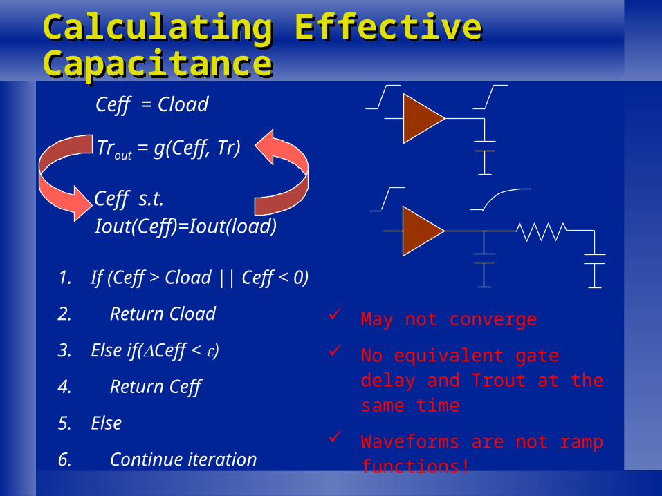
Calculating Effective CapacitanceCalculating Effective Capacitance
1. If (Ceff > Cload || Ceff < 0)
2. Return Cload
3. Else if(Ceff < )
4. Return Ceff
5. Else
6. Continue iteration
May not converge
No equivalent gate delay and Trout at the same time
Waveforms are not ramp functions!
Trout = g(Ceff, Tr)
Ceff s.t. Iout(Ceff)=Iout(load)
Ceff = Cload

Current-Based Transistor ModelCurrent-Based Transistor Model MOSFET is a voltage-controlled current source,
e.g., as in the alpha-power-law model
For a simple inverter, gate output current is given by one of the transistors
An equivalent inverter macro-model for an inverting complex gate
current-based gate modeling
Ids
Vgs V tW
Leff
P c
PvVgs V t Vds Pv Vgs V t
W
LeffP c Vgs V t Vds Pv Vgs V t
02( ) ( )
( ) ( )
/

Current-Based Gate ModelingCurrent-Based Gate Modeling Consists of a lookup table I(Vi, Vo) and C(Vi, Vo)
Transient analysis for output signal waveform
Vi I(Vi, Vo)
C
RVoVi
Voltage-Based Current-Based
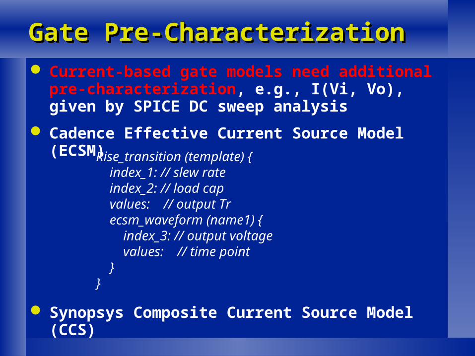
Gate Pre-CharacterizationGate Pre-Characterization Current-based gate models need additional pre-
characterization, e.g., I(Vi, Vo), given by SPICE DC sweep analysis
Cadence Effective Current Source Model (ECSM)
Synopsys Composite Current Source Model (CCS)
Rise_transition (template) { index_1: // slew rate index_2: // load cap values: // output Tr ecsm_waveform (name1) { index_3: // output voltage values: // time point }}

OutlineOutline
Gate Modeling Background
Problem Formulation
Approximation and Regression
Applications
Experiments
Conclusion

Constructing Current-Based Gate Model From Existing Timing LibrariesConstructing Current-Based Gate Model From Existing Timing Libraries
Given gate delays and output slew rates for load caps and input slew rates, find an equivalent current-based gate model, e.g., I(Vi, Vo) and C
Vi I(Vi, Vo)
C
1. Dg = f(Cload, Tr)
2. Trout = g(Cload, Tr)
Tr
Clo
ad
Dg
Tr
Clo
ad
TroutVo
Vi
I
C

To find an unknown underlying physical process by a set of measurements
Q = C V
Inhomogeneous Fredholm integral equations of the first kind
Inverse ProblemInverse Problem
outTrinTrDg
outTrinTrDg
ddL
inTrDg
ddL
VCCdtVoViI
VCCdtVoViI
5.05.0
5.05.0
5.0
0
))(2.08.0(),(
)(5.0),(
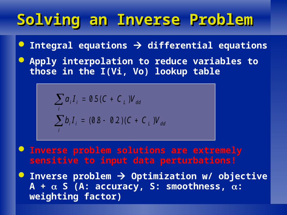
Integral equations differential equations
Apply interpolation to reduce variables to those in the I(Vi, Vo) lookup table
Inverse problem solutions are extremely sensitive to input data perturbations!
Inverse problem Optimization w/ objective A + S (A: accuracy, S: smoothness, : weighting factor)
Solving an Inverse ProblemSolving an Inverse Problem
a I C C V
b I C C V
i i L ddi
i i L ddi
0 5
0 8 0 2
. ( )
( . . )( )

OutlineOutline
Gate Modeling Background
Problem Formulation
Solution: Approximation and Regression
Applications
Experiments
Conclusion
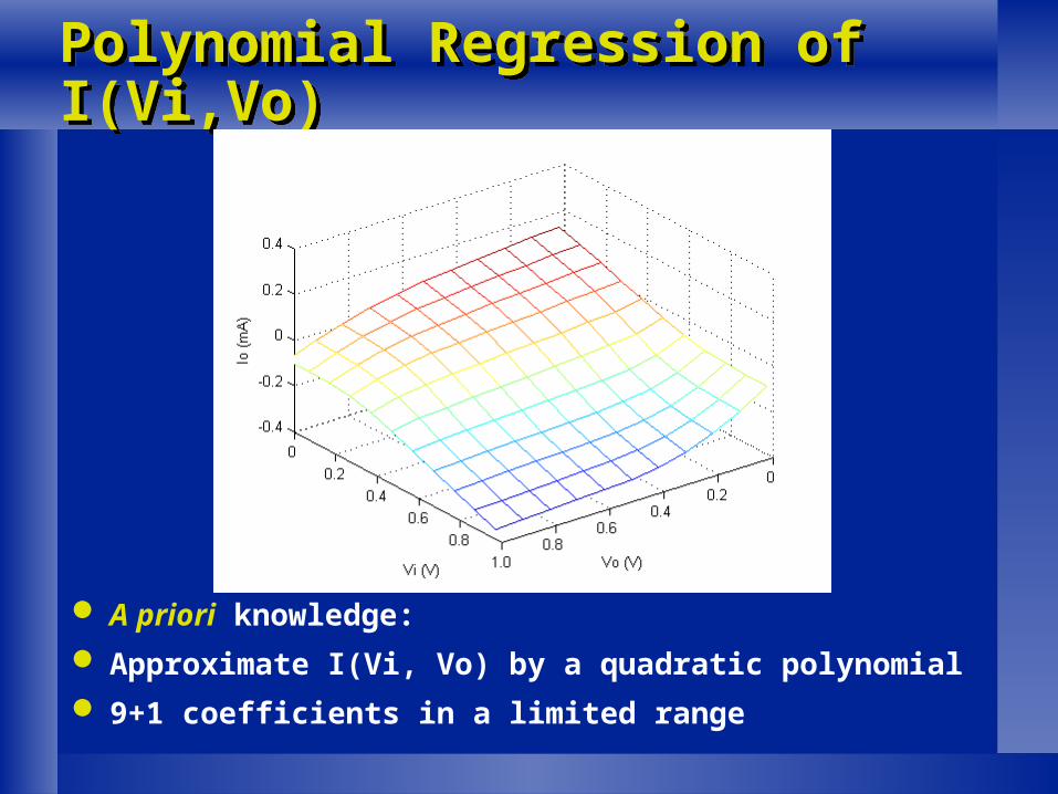
Polynomial Regression of I(Vi,Vo)Polynomial Regression of I(Vi,Vo)
A priori knowledge:
Approximate I(Vi, Vo) by a quadratic polynomial
9+1 coefficients in a limited range

Polynomial Regression of I(Vi,Vo)Polynomial Regression of I(Vi,Vo)
I V V a a V a V
a V a V V a V V
a V a V V a V V
i o o o
i i o i o
i i o i o
( , )
0 0 0 1 0 22
1 0 11 1 22
2 02
2 12
2 22 2
I
I
I
I
I V V
I V VV i i o
Vo i o
( , )
( , )
( , )
( , )
( , )
( , )
0 0
0 1
1 0
1 1
0
0
0
0
0
0
a a
a a a
a a a
a a a
a a a
a a a
0 0 2 0
0 1 0 2 1 0
0 0 0 1 0 2
0 0 1 0 2 0
0 1 11 2 1
1 0 11 1 2
0
0
0
0
0
0
,
, ,

1. Start with an initial polynomial coefficient
2. For each iteration
3. Perturb a coefficient ai’ = ai +
4. Compute mean square gate delay mismatch
5. If reduces, commit perturbation ai = ai +
6. Else, go other direction ai = ai –
7. Stop if no improvement
8. Reduce step for another iteration
9. Compute I(Vi, Vo) and C
Our Constructive Method Our Constructive Method

ApplicationsApplications
More accuracy, arbitrary waveform
Efficiency advantage over SPICE simulation
Gate delay calculation for Long interconnects
Cross-coupling interconnects
Supply voltage drop effect
Supply current calculation
Noise calculation

Supply Voltage Variation Effect on Gate Delay CalculationSupply Voltage Variation Effect on Gate Delay Calculation
There exists an equivalent inverter macro-model for each input combination for any (inverting) complex gate
Adjust input and output voltages for I(Vi, Vo) table lookup for a falling input signal, but not for a rising input signal
VVV
VVV
VVII
oo
ii
oi
'
'
)','('

ExperimentsExperiments BPTM 70nm technology cell library
Compare (our) constructed and (SPICE simulation based) pre-characterization models
Our Constructed
Quad. Pre -Characterization
Cubic Pre -Characterization
invx4 1.25 5.7 9.73 45.2 11.12 37.8
invx8 1.85 16.9 12.93 27.2 14.67 27.8
nor2x4 0.46 4.8 7.06 152.7 5.91 56.5

ExperimentsExperiments Gate delays by (1) our model and (2) pre-characterized
model normalized by SPICE simulation resultsFor Ideal (1.0V) Supply Voltage
(1) 93.0 97.4 99.0 101.0 97.8 94.9 95.7 98.0
(2) 100.0 98.7 99.3 100.0 102.5 101.2 100.6 100.0
(1) 98.4 102.6 99.0 95.5 103.9 100.8 100.2 99.5
(2) 104.3 101.8 100.0 100.0 97.6 98.5 99.2 100.1
For Degraded (0.9V) Supply Voltage
(1) 102.0 105.4 106.7 108.6 101.2 106.8 108.6 106.9
(2) 102.1 99.8 98.7 98.8 100.8 99.6 98.7 97.9
(1) 107.8 106.4 106.6 106.2 107.8 106.4 106.6 108.3
(2) 100.0 99.6 99.1 97.8 95.6 97.9 98.7 100.2

SummarySummary Utilize existing timing libraries for application of
novel current-based gate modeling
Wide range of applications: supply current calculation, delay calculation for complex waveforms, e.g., resistive shielding, crosstalk coupling, supply voltage variation, etc.
Slightly less accurate than pre-characterized current-based gate models, e.g., within 8.6% vs. 4.4% for gate delay calculation with varied supply voltage
Reasonable runtime for model construction, 28.3 seconds in average on a 2.8GHz P4 system

Thank you !Thank you !