Constant-Voltage Constant-Current Flyback ... · Constant-Voltage Constant-Current Flyback...
32
UCC28740 www.ti.com SLUSBF3A – JULY 2013 – REVISED JULY 2013 Constant-Voltage Constant-Current Flyback Controller Using Opto-Coupled Feedback Check for Samples: UCC28740 1FEATURES DESCRIPTION The UCC28740 isolated-flyback power-supply • Less than 10-mW No-Load Power Capability controller provides Constant-Voltage (CV) using an • Opto-Coupled Feedback for CV, and optical coupler to improve transient response to large- Primary-Side Regulation (PSR) for CC load steps. Constant-Current (CC) regulation is accomplished through Primary-side Regulation (PSR) • Enables ±1% Voltage Regulation and ±5% techniques. This device processes information from Current Regulation Across Line and Load opto-coupled feedback and an auxiliary flyback • 700-V Startup Switch winding for precise high-performance control of • 100-kHz Maximum Switching Frequency output voltage and current. Enables High-Power-Density Charger Designs An internal 700-V startup switch, dynamically- • Resonant-Ring Valley-Switching Operation for controlled operating states, and a tailored modulation Highest Overall Efficiency profile support ultra-low standby power without sacrificing startup time or output transient response. • Frequency Dithering to Ease EMI Compliance • Clamped Gate-Drive Output for MOSFET Control algorithms in the UCC28740 allow operating efficiencies to meet or exceed applicable standards. • Overvoltage, Low-Line, and Overcurrent The drive output interfaces to a MOSFET power Protection Functions switch. Discontinuous conduction mode (DCM) with • SOIC-7 Package valley-switching reduces switching losses. Modulation of switching frequency and primary current-peak APPLICATIONS amplitude (FM and AM) keeps the conversion efficiency high across the entire load and line ranges. • USB-Compliant Adapters and Chargers for Consumer Electronics The controller has a maximum switching frequency of 100 kHz and always maintains control of the peak- – Smart Phones primary current in the transformer. Protection features – Tablet Computers keep primary and secondary component stresses in – Cameras check. A minimum switching frequency of 170 Hz • Standby Supply for TV and Desktop facilitates the achievement of less than 10-mW no- load power. • White Goods TYPICAL V-I DIAGRAM SIMPLIFIED APPLICATION DIAGRAM 1 Please be aware that an important notice concerning availability, standard warranty, and use in critical applications of Texas Instruments semiconductor products and disclaimers thereto appears at the end of this data sheet. PRODUCTION DATA information is current as of publication date. Copyright © 2013, Texas Instruments Incorporated Products conform to specifications per the terms of the Texas Instruments standard warranty. Production processing does not necessarily include testing of all parameters.
-
Upload
truongdang -
Category
Documents
-
view
275 -
download
0
Transcript of Constant-Voltage Constant-Current Flyback ... · Constant-Voltage Constant-Current Flyback...
UCC28740
www.ti.com SLUSBF3A –JULY 2013–REVISED JULY 2013
Constant-Voltage Constant-Current Flyback Controller Using Opto-Coupled FeedbackCheck for Samples: UCC28740
1FEATURES DESCRIPTIONThe UCC28740 isolated-flyback power-supply• Less than 10-mW No-Load Power Capabilitycontroller provides Constant-Voltage (CV) using an• Opto-Coupled Feedback for CV, and optical coupler to improve transient response to large-
Primary-Side Regulation (PSR) for CC load steps. Constant-Current (CC) regulation isaccomplished through Primary-side Regulation (PSR)• Enables ±1% Voltage Regulation and ±5%techniques. This device processes information fromCurrent Regulation Across Line and Loadopto-coupled feedback and an auxiliary flyback• 700-V Startup Switch winding for precise high-performance control of
• 100-kHz Maximum Switching Frequency output voltage and current.Enables High-Power-Density Charger Designs
An internal 700-V startup switch, dynamically-• Resonant-Ring Valley-Switching Operation for controlled operating states, and a tailored modulation
Highest Overall Efficiency profile support ultra-low standby power withoutsacrificing startup time or output transient response.• Frequency Dithering to Ease EMI Compliance
• Clamped Gate-Drive Output for MOSFET Control algorithms in the UCC28740 allow operatingefficiencies to meet or exceed applicable standards.• Overvoltage, Low-Line, and OvercurrentThe drive output interfaces to a MOSFET powerProtection Functionsswitch. Discontinuous conduction mode (DCM) with• SOIC-7 Package valley-switching reduces switching losses. Modulationof switching frequency and primary current-peakAPPLICATIONS amplitude (FM and AM) keeps the conversionefficiency high across the entire load and line ranges.• USB-Compliant Adapters and Chargers for
Consumer Electronics The controller has a maximum switching frequency of100 kHz and always maintains control of the peak-– Smart Phonesprimary current in the transformer. Protection features– Tablet Computerskeep primary and secondary component stresses in
– Cameras check. A minimum switching frequency of 170 Hz• Standby Supply for TV and Desktop facilitates the achievement of less than 10-mW no-
load power.• White Goods
TYPICAL V-I DIAGRAMSIMPLIFIED APPLICATION DIAGRAM
1
Please be aware that an important notice concerning availability, standard warranty, and use in critical applications ofTexas Instruments semiconductor products and disclaimers thereto appears at the end of this data sheet.
PRODUCTION DATA information is current as of publication date. Copyright © 2013, Texas Instruments IncorporatedProducts conform to specifications per the terms of the TexasInstruments standard warranty. Production processing does notnecessarily include testing of all parameters.
UCC28740
SLUSBF3A –JULY 2013–REVISED JULY 2013 www.ti.com
This integrated circuit can be damaged by ESD. Texas Instruments recommends that all integrated circuits be handled withappropriate precautions. Failure to observe proper handling and installation procedures can cause damage.
ESD damage can range from subtle performance degradation to complete device failure. Precision integrated circuits may be moresusceptible to damage because very small parametric changes could cause the device not to meet its published specifications.
PRODUCT INFORMATION (1)
PACKAGE PINS ORDERABLE MINIMUM SWITCHING OPTIONSDEVICES FREQUENCY (Hz)SOIC (D) 7 UCC28740D 170
(1) See Orderable Addendum for specific device ordering information.
ABSOLUTE MAXIMUM RATINGS (1)
MIN MAX UNITStart-up pin voltage, HV VHV 700
VBias supply voltage, VDD VVDD 38Continuous gate-current sink IDRV 50Continuous gate-current source IDRV Self-limiting
mAPeak current, VS IFB 1Peak current, FB IVS −1.2Gate-drive voltage at DRV VDRV −0.5 Self-limiting
CS −0.5 5V
Voltage range FB −0.5 7VS −0.75 7
Operating junction temperature range TJ −55 150Storage temperature TSTG −65 150 °CLead temperature 0.6 mm from case for 10 seconds 260
Human-body model (HBM) 2000ESD rating V
Charged-device model (CDM) 500
(1) Stresses beyond those listed under absolute maximum ratings may cause permanent damage to the device. These are stress ratingsonly and functional operation of the device at these or any other conditions beyond those indicated under recommended operatingconditions is not implied. Exposure to absolute-maximum-rated conditions for extended periods may affect device reliability. All voltagesare with respect to GND. Currents are positive into, negative out of the specified terminal. These ratings apply over the operatingambient temperature ranges unless otherwise noted.
2 Submit Documentation Feedback Copyright © 2013, Texas Instruments Incorporated
Product Folder Links: UCC28740

UCC28740
www.ti.com SLUSBF3A –JULY 2013–REVISED JULY 2013
RECOMMENDED OPERATING CONDITIONSover operating free-air temperature range (unless otherwise noted)
MIN TYP MAX UNITVVDD Bias-supply operating voltage 9 35 VCVDD VDD bypass capacitor 0.047 µFIFB Feedback current, continuous 50 µAIVS VS pin current, out of pin 1 mATJ Operating junction temperature −20 125 °C
THERMAL INFORMATIONUCC28740
THERMAL METRIC (1) D UNITS7 PINS
θJA Junction-to-ambient thermal resistance (2) 141.5θJCtop Junction-to-case (top) thermal resistance (3) 73.8θJB Junction-to-board thermal resistance (4) 89.0 °C/WψJT Junction-to-top characterization parameter (5) 23.5ψJB Junction-to-board characterization parameter (6) 88.2
(1) For more information about traditional and new thermal metrics, see the IC Package Thermal Metrics application report, SPRA953.(2) The junction-to-ambient thermal resistance under natural convection is obtained in a simulation on a JEDEC-standard, high-K board, as
specified in JESD51-7, in an environment described in JESD51-2a.(3) The junction-to-case (top) thermal resistance is obtained by simulating a cold plate test on the package top. No specific JEDEC-
standard test exists, but a close description can be found in the ANSI SEMI standard G30-88.(4) The junction-to-board thermal resistance is obtained by simulating in an environment with a ring cold plate fixture to control the PCB
temperature, as described in JESD51-8.(5) The junction-to-top characterization parameter, ψJT, estimates the junction temperature of a device in a real system and is extracted
from the simulation data for obtaining θJA, using a procedure described in JESD51-2a (sections 6 and 7).(6) The junction-to-board characterization parameter, ψJB, estimates the junction temperature of a device in a real system and is extracted
from the simulation data for obtaining θJA , using a procedure described in JESD51-2a (sections 6 and 7).
Copyright © 2013, Texas Instruments Incorporated Submit Documentation Feedback 3
Product Folder Links: UCC28740
UCC28740
SLUSBF3A –JULY 2013–REVISED JULY 2013 www.ti.com
ELECTRICAL CHARACTERISTICSover operating free-air temperature range, VVDD = 25 V, HV = open, VFB = 0 V, VVS = 4 V, TA = –40°C to +125°C, TJ = TA(unless otherwise noted)
PARAMETER TEST CONDITIONS MIN TYP MAX UNITSHIGH-VOLTAGE START UPIHV Start-up current out of VDD VHV = 100 V, VVDD = 0 V, start state 100 250 500
µAIHVLKG25 Leakage current at HV VHV = 400 V, run state, TJ = 25°C 0.01 0.5BIAS SUPPLY INPUTIRUN Supply current, run IDRV = 0, run state 2 2.65 mAIWAIT Supply current, wait IDRV = 0, wait state 95 125ISTART Supply current, start IDRV = 0, VVDD = 18 V, start state, IHV = 0 18 30 µAIFAULT Supply current, fault IDRV = 0, fault state 95 130UNDERVOLTAGE LOCKOUTVVDD(on) VDD turnon threshold VVDD low to high 19 21 23
VVVDD(off) VDD turnoff threshold VVDD high to low 7.35 7.75 8.15VS INPUTVVSNC Negative clamp level IVSLS = –300 µA, volts below ground 190 250 325 mVIVSB Input bias current VVS = 4 V –0.25 0 0.25 µAFB INPUTIFBMAX Full-range input current fSW = fSW(min) 16 23 30 µAVFBMAX Input voltage at full range IFB = 25 µA, TJ = 25°C 0.75 0.88 1 V
ΔIFB = 20 µA, centered at IFB = 15 µA, TJ =RFB FB-input resistance, linearized 10 14 18 kΩ25°CCS INPUTVCST(max) Maximum CS threshold voltage IFB = 0 µA (1) 738 773 810
mVVCST(min) Minimum CS threshold voltage IFB = 35 µA (1) 170 194 215KAM AM-control ratio VCST(max) / VCST(min) 3.6 4 4.45 V/VVCCR Constant-current regulation factor 318 330 343 mVKLC Line-compensation current ratio IVSLS = –300 µA, IVSLS / current out of CS pin 24 25 28.6 A/AtCSLEB Leading-edge blanking time DRV output duration, V CS = 1 V 180 230 280 nsDRIVERSIDRS DRV source current VDRV = 8 V, VVDD = 9 V 20 25 mARDRVLS DRV low-side drive resistance IDRV = 10 mA 6 12 ΩVDRCL DRV clamp voltage VVDD = 35 V 14 16 VRDRVSS DRV pulldown in start-state 150 190 230 kΩTIMINGfSW(max) Maximum switching frequency IFB = 0 µA (1) 91 100 106 kHzfSW(min) Minimum switching frequency IFB = 35 µA (1) 140 170 210 HztZTO Zero-crossing timeout delay 1.8 2.1 2.55 µs
(1) This device automatically varies the control frequency and current sense thresholds to improve EMI performance. These thresholdvoltages and frequency limits represent average levels.
4 Submit Documentation Feedback Copyright © 2013, Texas Instruments Incorporated
Product Folder Links: UCC28740
UCC28740
www.ti.com SLUSBF3A –JULY 2013–REVISED JULY 2013
ELECTRICAL CHARACTERISTICS (continued)over operating free-air temperature range, VVDD = 25 V, HV = open, VFB = 0 V, VVS = 4 V, TA = –40°C to +125°C, TJ = TA(unless otherwise noted)
PARAMETER TEST CONDITIONS MIN TYP MAX UNITSPROTECTIONVOVP Overvoltage threshold At VS input, TJ = 25°C (2) 4.52 4.6 4.71
VVOCP Overcurrent threshold At CS input 1.4 1.5 1.6IVSL(run) VS line-sense run current Current out of VS pin increasing 190 225 275
µAIVSL(stop) VS line-sense stop current Current out of VS pin decreasing 70 80 100KVSL VS line sense ratio IVSL(run) / IVSL(stop) 2.45 2.8 3.05 A/ATJ(stop) Thermal-shutdown temperature Internal junction temperature 165 °C
(2) The overvoltage threshold level at VS decreases with increasing temperature by 0.8 mV/°C. This compensation is included to reduce thepower-supply output overvoltage detection variance over temperature.
Copyright © 2013, Texas Instruments Incorporated Submit Documentation Feedback 5
Product Folder Links: UCC28740
UCC28740
SLUSBF3A –JULY 2013–REVISED JULY 2013 www.ti.com
DEVICE INFORMATIONFunctional Block Diagram
Figure 1. Functional Block Diagram
6 Submit Documentation Feedback Copyright © 2013, Texas Instruments Incorporated
Product Folder Links: UCC28740
UCC28740
www.ti.com SLUSBF3A –JULY 2013–REVISED JULY 2013
SOIC (D) PACKAGE7 PINS
(TOP VIEW)
PIN FUNCTIONSPIN
I/O DESCRIPTIONNAME NO.
The current-sense (CS) input connects to a ground-referenced current-sense resistor in series withthe power switch. The resulting voltage monitors and controls the peak primary current. A seriesCS 5 I resistor is added to this pin to compensate for peak switch-current levels as the AC-mains inputvaries.Drive (DRV) is an output that drives the gate of an external high-voltage MOSFET switchingDRV 6 O transistor.The feedback (FB) input receives a current signal from the optocoupler output transistor. An internalcurrent mirror divides the feedback current by 2.5 and applies it to an internal pullup resistor toFB 3 I generate a control voltage, VCL. The voltage at this resistor directly drives the control law function,which determines the switching frequency and the peak amplitude of the switching current .The ground (GND) pin is both the reference pin for the controller, and the low-side return for the drive
GND 4 — output. Special care must be taken to return all AC-decoupling capacitors as close as possible to thispin and avoid any common trace length with analog signal-return paths.The high-voltage (HV) pin may connect directly, or through a series resistor, to the rectified bulkHV 7 I voltage and provides a charge to the VDD capacitor for the startup of the power supply.VDD is the bias-supply input pin to the controller. A carefully-placed bypass capacitor to GND isVDD 1 I required on this pin.Voltage sense (VS) is an input used to provide demagnetization timing feedback to the controller tolimit frequency, to control constant-current operation, and to provide output-overvoltage detection. VSis also used for AC-mains input-voltage detection for peak primary-current compensation. This pinVS 2 I connects to a voltage divider between an auxiliary winding and GND. The value of the upper resistorof this divider programs the AC-mains run and stop thresholds, and factors into line compensation atthe CS pin.
Copyright © 2013, Texas Instruments Incorporated Submit Documentation Feedback 7
Product Folder Links: UCC28740
UCC28740
SLUSBF3A –JULY 2013–REVISED JULY 2013 www.ti.com
Detailed Pin DescriptionVDD (Device Bias Voltage Supply) The VDD pin connects to a bypass capacitor-to-ground. The turnon UVLO
threshold is 21 V and turnoff UVLO threshold is 7.75 V with an available operating range up to 35 V onVDD. The typical USB-charging specification requires the output current to operate in constant-currentmode from 5 V down to at least 2 V which is achieved easily with a nominal VVDD of approximately 25 V.The additional VDD headroom up to 35 V allows for VVDD to rise due to the leakage energy delivered tothe VDD capacitor during high-load conditions.
GND (Ground) UCC28740 has a single ground reference external to the device for the gate-drive current andanalog signal reference. Place the VDD-bypass capacitor close to GND and VDD with short traces tominimize noise on the VS, FB, and CS signal pins.
HV (High-Voltage Startup) The HV pin connects directly to the bulk capacitor to provide a startup current to theVDD capacitor. The typical startup current is approximately 250 µA which provides fast charging of theVDD capacitor. The internal HV startup device is active until VVDD exceeds the turnon UVLO threshold of21 V at which time the HV startup device turns off. In the off state the HV leakage current is very low tominimize standby losses of the controller. When VVDD falls below the 7.75 V UVLO turnoff threshold theHV startup device turns on.
VS (Voltage Sense) The VS pin connects to a resistor-divider from the auxiliary winding to ground. The auxiliaryvoltage waveform is sampled at the end of the transformer secondary-current demagnetization time toprovide accurate control of the output current when in constant-current mode. The waveform on the VSpin determines the timing information to achieve valley-switching, and the timing to control the duty-cycleof the transformer secondary current. Avoid placing a filter capacitor on this input which interferes withaccurate sensing of this waveform.During the MOSFET on-time, this pin also senses VS current generated through RS1 by the reflected bulk-capacitor voltage to provide for AC-input run and stop thresholds, and to compensate the current-sensethreshold across the AC-input range. For the AC-input run/stop function, the run threshold on VS is 225µA and the stop threshold is 80 µA.At the end of off-time demagnetization, the reflected output voltage is sampled at this pin to provide outputovervoltage protection. The values for the auxiliary voltage-divider upper-resistor, RS1, and lower-resistor,RS2, are determined by Equation 1 and Equation 2.
where• NPA is the transformer primary-to-auxiliary turns-ratio,• VIN(run) is the AC RMS voltage to enable turnon of the controller (run),
(in case of DC input, leave out the √2 term in the equation),• IVSL(run) is the run-threshold for the current pulled out of the VS pin during the switch on-time (see
ELECTRICAL CHARACTERISTICS). (1)
where• VOV is the maximum allowable peak voltage at the converter output,• VF is the output-rectifier forward drop at near-zero current,• NAS is the transformer auxiliary-to-secondary turns-ratio,• RS1 is the VS divider high-side resistance,• VOVP is the overvoltage detection threshold at the VS input (see ELECTRICAL CHARACTERISTICS). (2)
8 Submit Documentation Feedback Copyright © 2013, Texas Instruments Incorporated
Product Folder Links: UCC28740
LC S1 CS D PALC
P
K R R t NR
L
´ ´ ´ ´
=
CCR PSCS XFMR
OCC
V NR
2I
´= ´ h
UCC28740
www.ti.com SLUSBF3A –JULY 2013–REVISED JULY 2013
FB (Feedback) The FB pin connects to the emitter of an analog-optocoupler output transistor which usually hasthe collector connected to VDD. The current supplied to FB by the optocoupler is reduced internally by afactor of 2.5 and the resulting current is applied to an internal 480-kΩ resistor to generate the control lawvoltage (VCL). This VCL directly determines the converter switching frequency and peak primary currentrequired for regulation per the control-law for any given line and load condition.
DRV (Gate Drive) The DRV pin connects to the MOSFET gate pin, usually through a series resistor. The gatedriver provides a gate-drive signal limited to 14 V. The turnon characteristic of the driver is a 25-mAcurrent source which limits the turnon dv/dt of the MOSFET drain and reduces the leading-edge currentspike while still providing a gate-drive current to overcome the Miller plateau. The gate-drive turnoffcurrent is determined by the RDSON of the low-side driver along with any external gate-drive resistance.Adding external gate resistance reduces the MOSFET drain turn-off dv/dt, if necessary.
CS (Current Sense) The current-sense pin connects through a series resistor (RLC) to the current-sense resistor(RCS). The maximum current-sense threshold (VCST(max)) is 0.773 V for IPP(max), and the minimum current-sense threshold (VCST(min)) is 0.194 V for IPP(min). RLC provides the feed-forward line compensation toeliminate changes in IPP with input voltage due to the propagation delay of the internal comparator andMOSFET turnoff time. An internal leading-edge blanking time of 235 ns eliminates sensitivity to theMOSFET turnon current spike. Placing a bypass capacitor on the CS pin is unnecessary. The targetoutput current in constant-current (CC) regulation determines the value of RCS. The values of RCS and RLCare calculated using Equation 3 and Equation 4. The term VCCR is the product of the demagnetizationconstant, 0.425, and VCST(max). VCCRis held to a tighter accuracy than either of its constituent terms. Theterm ηXFMR accounts for the energy stored in the transformer but not delivered to the secondary. This termincludes transformer resistance and core loss, bias power, and primary-to-secondary leakage ratio.
Example:With a transformer core and winding loss of 5%, primary-to-secondary leakage inductance of 3.5%, and biaspower to output power ratio of 0.5%, the ηXFMR value at full power is approximately: 1 - 0.05 - 0.035 - 0.005 =0.91.
where• VCCR is a constant-current regulation factor (see ELECTRICAL CHARACTERISTICS),• NPS is the transformer primary-to-secondary turns-ratio (a ratio of 13 to 15 is typical for 5-V output),• IOCC is the target output current in constant-current regulation,• ηXFMR is the transformer efficiency at full power. (3)
where• RS1 is the VS pin high-side resistor value,• RCS is the current-sense resistor value,• tD is the total current-sense delay consisting of MOSFET turnoff delay, plus approximately 50 ns internal delay,• NPA is the transformer primary-to-auxiliary turns-ratio,• LP is the transformer primary inductance,• KLC is a current-scaling constant for line compensation (see ELECTRICAL CHARACTERISTICS). (4)
Copyright © 2013, Texas Instruments Incorporated Submit Documentation Feedback 9
Product Folder Links: UCC28740
0
40
80
120
160
200
240
280
320
-50 -25 0 25 50 75 100 125
I HV -
HV
Sta
rtup
Cur
rent
(µ
A)
TJ - Temperature (oC) C003
VHV = 100 V, VVDD = 0 V
0
50
100
150
200
250
300
-50 -25 0 25 50 75 100 125
VS
Lin
e-S
ense
Cur
rent
(µ
A)
TJ - Temperature (oC) C004
IVSL(run)
IVSL(stop)
0.0001
0.001
0.01
0.1
1
10
0 5 10 15 20 25 30 35
I VD
D -
Bia
s-S
uppl
y C
urre
nt
(mA
)
VDD - Bias-Supply Voltage (V) C001
HV = Open Run State
Wait State
Start State
VDD Turn-On VDD Turn-Off
0.0001
0.001
0.01
0.1
1
10
-50 -25 0 25 50 75 100 125I V
DD -
Bia
s-S
uppl
y C
urre
nt
(mA
)
TJ - Temperature (oC) C002
HV = Open IRUN, VDD = 25 V
IWAIT, VDD = 25 V
ISTART, VDD = 18 V
UCC28740
SLUSBF3A –JULY 2013–REVISED JULY 2013 www.ti.com
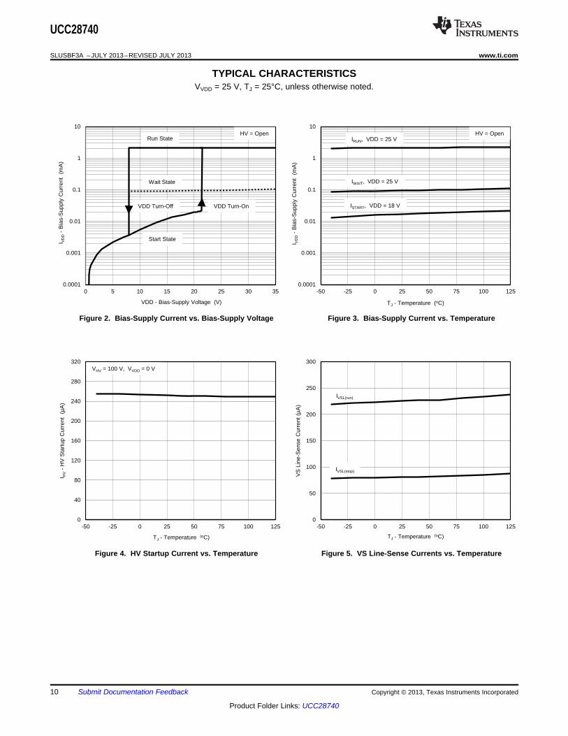
TYPICAL CHARACTERISTICSVVDD = 25 V, TJ = 25°C, unless otherwise noted.
Figure 2. Bias-Supply Current vs. Bias-Supply Voltage Figure 3. Bias-Supply Current vs. Temperature
Figure 4. HV Startup Current vs. Temperature Figure 5. VS Line-Sense Currents vs. Temperature
10 Submit Documentation Feedback Copyright © 2013, Texas Instruments Incorporated
Product Folder Links: UCC28740
140
150
160
170
180
190
200
-50 -25 0 25 50 75 100 125
f SW
(min
) - M
inim
um S
witc
hing
Fre
quen
cy
(Hz)
TJ - Temperature (oC) C007
20
22
24
26
28
30
32
34
-50 -25 0 25 50 75 100 125
I DR
S -
DR
V S
ourc
e C
urre
nt
(mA
)
TJ - Temperature (oC) C008
VDRV = 8 V, VVDD = 9 V
170
175
180
185
190
195
200
205
210
-50 -25 0 25 50 75 100 125
VC
ST
(min
) - M
inim
um C
S T
hres
hold
Vol
tage
(m
V)
TJ - Temperature (oC) C005
310
315
320
325
330
335
340
345
350
-50 -25 0 25 50 75 100 125
VC
CR -
Con
stan
t-C
urre
nt R
egul
atio
n F
acto
r (
mV
) TJ - Temperature (oC)
C006
UCC28740
www.ti.com SLUSBF3A –JULY 2013–REVISED JULY 2013
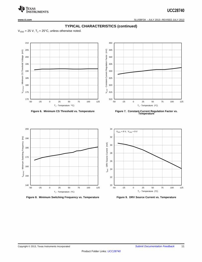
TYPICAL CHARACTERISTICS (continued)VVDD = 25 V, TJ = 25°C, unless otherwise noted.
Figure 6. Minimum CS Threshold vs. Temperature Figure 7. Constant-Current Regulation Factor vs.Temperature
Figure 8. Minimum Switching Frequency vs. Temperature Figure 9. DRV Source Current vs. Temperature
Copyright © 2013, Texas Instruments Incorporated Submit Documentation Feedback 11
Product Folder Links: UCC28740
0.0
0.1
0.2
0.3
0.4
0.5
0.6
0.7
0.8
0.9
1.0
0 5 10 15 20 25 30 35
VF
B -
FB
Inpu
t V
olta
ge
(V)
IFB - FB Input Current (µA) C009
4.52
4.54
4.56
4.58
4.60
4.62
4.64
4.66
4.68
-50 -25 0 25 50 75 100 125
VO
VP -
VS
Ove
rvol
tage
Thr
esho
ld
(V)
TJ - Temperature (oC) C010
UCC28740
SLUSBF3A –JULY 2013–REVISED JULY 2013 www.ti.com
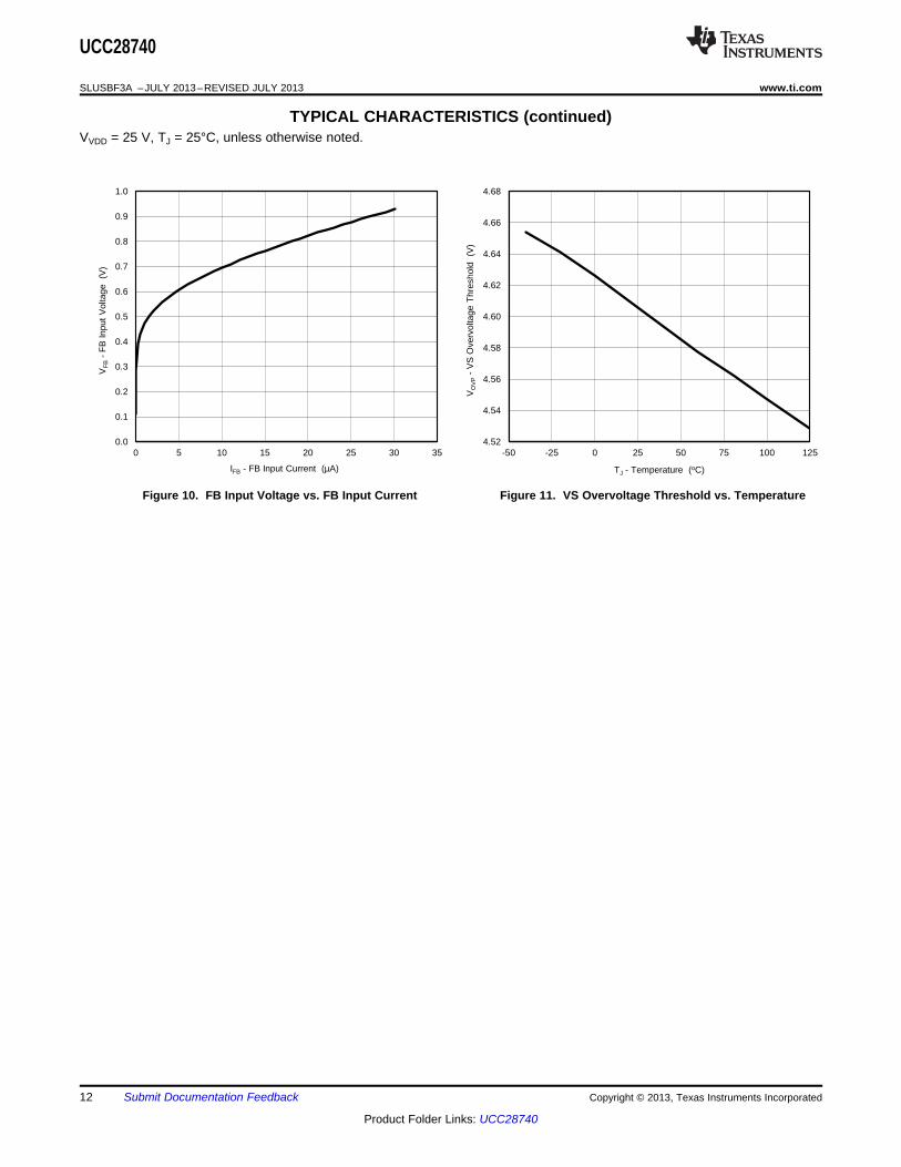
TYPICAL CHARACTERISTICS (continued)VVDD = 25 V, TJ = 25°C, unless otherwise noted.
Figure 10. FB Input Voltage vs. FB Input Current Figure 11. VS Overvoltage Threshold vs. Temperature
12 Submit Documentation Feedback Copyright © 2013, Texas Instruments Incorporated
Product Folder Links: UCC28740
UCC28740
www.ti.com SLUSBF3A –JULY 2013–REVISED JULY 2013
FUNCTIONAL DESCRIPTION
The UCC28740 is a flyback power-supply controller which provides high-performance voltage regulation using anoptically-coupled feedback signal from a secondary-side voltage regulator. The device provides accurateconstant-current regulation using primary-side feedback. The controller operates in discontinuous-conductionmode (DCM) with valley-switching to minimize switching losses. The control law scheme combines frequencywith primary peak-current amplitude modulation to provide high conversion efficiency across the load range. Thecontrol law provides a wide dynamic operating range of output power which allows the power-supply designer toeasily achieve less than 30-mW standby power dissipation using a standard shunt-regulator and optocoupler. Fora target of less than 10-mW standby power, careful loss-management design with a low-power regulator andhigh-CTR optocoupler is required.
During low-power operating conditions, the power-management features of the controller reduce the device-operating current at switching frequencies below 32 kHz. At and above this frequency, the UCC28740 includesfeatures in the modulator to reduce the EMI peak energy of the fundamental switching frequency and harmonics.A complete low-cost and low component-count charger-solution is realized using a straight-forward designprocess.
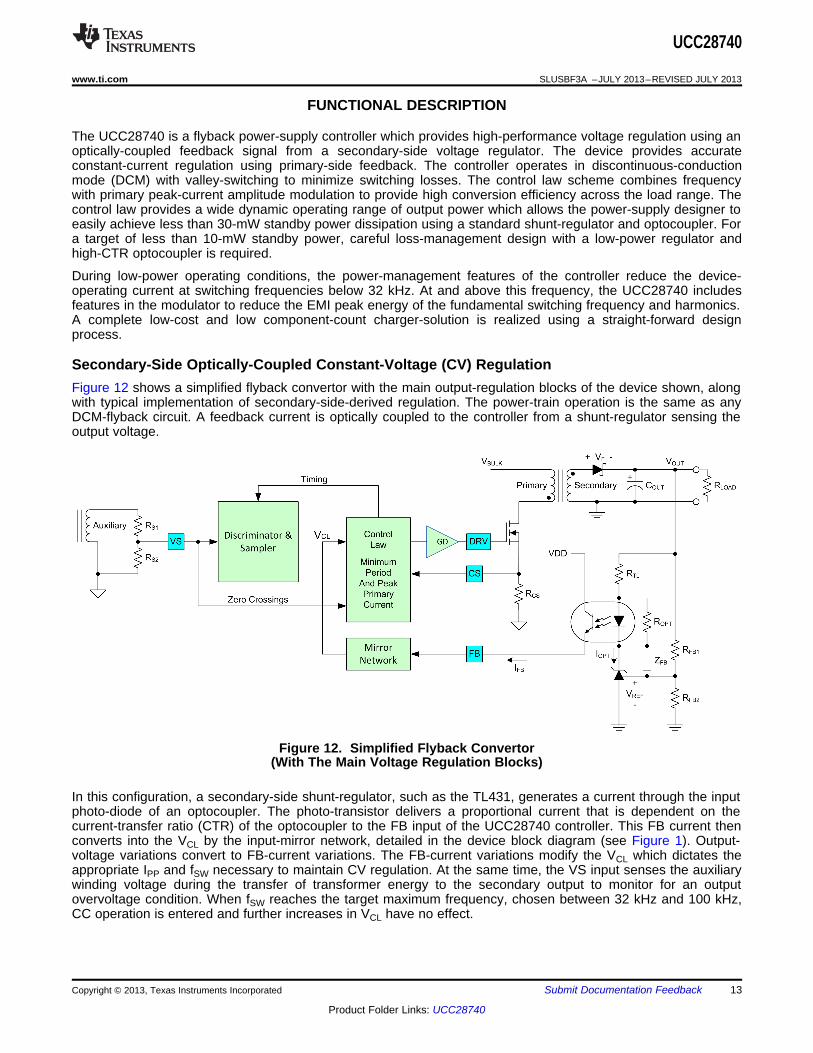
Secondary-Side Optically-Coupled Constant-Voltage (CV) RegulationFigure 12 shows a simplified flyback convertor with the main output-regulation blocks of the device shown, alongwith typical implementation of secondary-side-derived regulation. The power-train operation is the same as anyDCM-flyback circuit. A feedback current is optically coupled to the controller from a shunt-regulator sensing theoutput voltage.
Figure 12. Simplified Flyback Convertor(With The Main Voltage Regulation Blocks)
In this configuration, a secondary-side shunt-regulator, such as the TL431, generates a current through the inputphoto-diode of an optocoupler. The photo-transistor delivers a proportional current that is dependent on thecurrent-transfer ratio (CTR) of the optocoupler to the FB input of the UCC28740 controller. This FB current thenconverts into the VCL by the input-mirror network, detailed in the device block diagram (see Figure 1). Output-voltage variations convert to FB-current variations. The FB-current variations modify the VCL which dictates theappropriate IPP and fSW necessary to maintain CV regulation. At the same time, the VS input senses the auxiliarywinding voltage during the transfer of transformer energy to the secondary output to monitor for an outputovervoltage condition. When fSW reaches the target maximum frequency, chosen between 32 kHz and 100 kHz,CC operation is entered and further increases in VCL have no effect.
Copyright © 2013, Texas Instruments Incorporated Submit Documentation Feedback 13
Product Folder Links: UCC28740
UCC28740
SLUSBF3A –JULY 2013–REVISED JULY 2013 www.ti.com
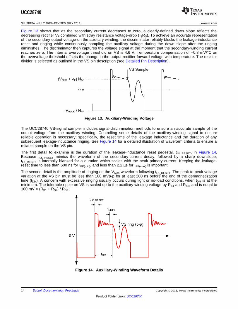
Figure 13 shows that as the secondary current decreases to zero, a clearly-defined down slope reflects thedecreasing rectifier VF combined with stray resistance voltage-drop (ISRS). To achieve an accurate representationof the secondary output voltage on the auxiliary winding, the discriminator reliably blocks the leakage-inductancereset and ringing while continuously sampling the auxiliary voltage during the down slope after the ringingdiminishes. The discriminator then captures the voltage signal at the moment that the secondary-winding currentreaches zero. The internal overvoltage threshold on VS is 4.6 V. Temperature compensation of –0.8 mV/°C onthe overvoltage threshold offsets the change in the output-rectifier forward voltage with temperature. The resistordivider is selected as outlined in the VS pin description (see Detailed Pin Description).
Figure 13. Auxiliary-Winding Voltage
The UCC28740 VS-signal sampler includes signal-discrimination methods to ensure an accurate sample of theoutput voltage from the auxiliary winding. Controlling some details of the auxiliary-winding signal to ensurereliable operation is necessary; specifically, the reset time of the leakage inductance and the duration of anysubsequent leakage-inductance ringing. See Figure 14 for a detailed illustration of waveform criteria to ensure areliable sample on the VS pin.
The first detail to examine is the duration of the leakage-inductance reset pedestal, tLK_RESET, in Figure 14.Because tLK_RESET mimics the waveform of the secondary-current decay, followed by a sharp downslope,tLK_RESET is internally blanked for a duration which scales with the peak primary current. Keeping the leakage-reset time to less than 600 ns for IPP(min), and less than 2.2 µs for IPP(max) is important.
The second detail is the amplitude of ringing on the VAUX waveform following tLK_RESET. The peak-to-peak voltagevariation at the VS pin must be less than 100 mVp-p for at least 200 ns before the end of the demagnetizationtime (tDM). A concern with excessive ringing usually occurs during light or no-load conditions, when tDM is at theminimum. The tolerable ripple on VS is scaled up to the auxiliary-winding voltage by RS1 and RS2, and is equal to100 mV × (RS1 + RS2) / RS2 .
Figure 14. Auxiliary-Winding Waveform Details
14 Submit Documentation Feedback Copyright © 2013, Texas Instruments Incorporated
Product Folder Links: UCC28740
UCC28740
www.ti.com SLUSBF3A –JULY 2013–REVISED JULY 2013
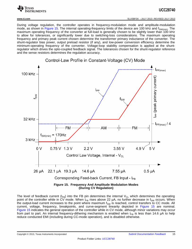
During voltage regulation, the controller operates in frequency-modulation mode and amplitude-modulationmode, as shown in Figure 15. The internal operating-frequency limits of the device are 100 kHz and fSW(min). Themaximum operating frequency of the converter at full-load is generally chosen to be slightly lower than 100 kHzto allow for tolerances, or significantly lower due to switching-loss considerations. The maximum operatingfrequency and primary peak current chosen determine the transformer primary inductance of the converter. Theshunt-regulator bias power, output preload resistor (if any), and low-power conversion efficiency determine theminimum-operating frequency of the converter. Voltage-loop stability compensation is applied at the shunt-regulator which drives the opto-coupled feedback signal. The tolerances chosen for the shunt-regulator referenceand the sense resistors determines the regulation accuracy.
Figure 15. Frequency And Amplitude Modulation Modes(During CV Regulation)
The level of feedback current (IFB) into the FB pin determines the internal VCL which determines the operatingpoint of the controller while in CV mode. When IFB rises above 22 µA, no further decrease in fSW occurs. Whenthe output-load current increases to the point where maximum fSW is reached, control transfers to CC mode. Allcurrent, voltage, frequency, breakpoints, and curve-segment linearity depicted in Figure 15 are nominal.Figure 15 indicates the general operation of the controller while in CV mode, although minor variations may occurfrom part to part. An internal frequency-dithering mechanism is enabled when IFB is less than 14.6 µA to helpreduce conducted EMI (including during CC-mode operation), and is disabled otherwise.
Copyright © 2013, Texas Instruments Incorporated Submit Documentation Feedback 15
Product Folder Links: UCC28740
PP P DMOUT
S SW
I N tI
2 N t= ´ ´
UDG-12203
tON tDM
tSW
IPP IS × NS/NP
UCC28740
SLUSBF3A –JULY 2013–REVISED JULY 2013 www.ti.com
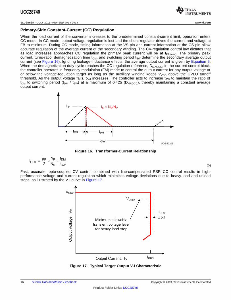
Primary-Side Constant-Current (CC) RegulationWhen the load current of the converter increases to the predetermined constant-current limit, operation entersCC mode. In CC mode, output voltage regulation is lost and the shunt-regulator drives the current and voltage atFB to minimum. During CC mode, timing information at the VS pin and current information at the CS pin allowaccurate regulation of the average current of the secondary winding. The CV-regulation control law dictates thatas load increases approaches CC regulation the primary peak current will be at IPP(max). The primary peakcurrent, turns-ratio, demagnetization time tDM, and switching period tSW determine the secondary average outputcurrent (see Figure 16). Ignoring leakage-inductance effects, the average output current is given by Equation 5.When the demagnetization duty-cycle reaches the CC-regulation reference, DMAGCC, in the current-control block,the controller operates in frequency modulation (FM) mode to control the output current for any output voltage ator below the voltage-regulation target as long as the auxiliary winding keeps VVDD above the UVLO turnoffthreshold. As the output voltage falls, tDM increases. The controller acts to increase tSW to maintain the ratio oftDM to switching period (tDM / tSW) at a maximum of 0.425 (DMAGCC), thereby maintaining a constant averageoutput current.
Figure 16. Transformer-Current Relationship
(5)
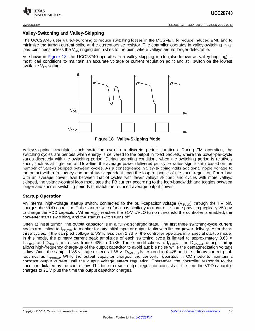
Fast, accurate, opto-coupled CV control combined with line-compensated PSR CC control results in high-performance voltage and current regulation which minimizes voltage deviations due to heavy load and unloadsteps, as illustrated by the V-I curve in Figure 17.
Figure 17. Typical Target Output V-I Characteristic
16 Submit Documentation Feedback Copyright © 2013, Texas Instruments Incorporated
Product Folder Links: UCC28740
UCC28740
www.ti.com SLUSBF3A –JULY 2013–REVISED JULY 2013
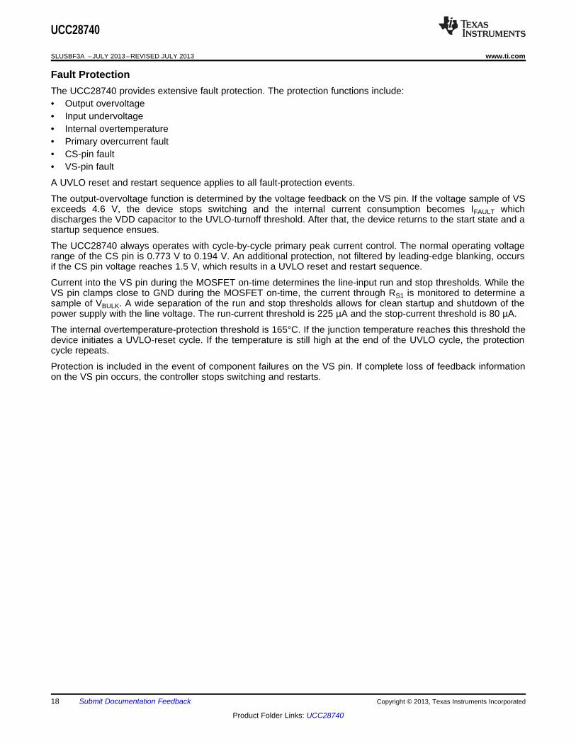
Valley-Switching and Valley-SkippingThe UCC28740 uses valley-switching to reduce switching losses in the MOSFET, to reduce induced-EMI, and tominimize the turnon current spike at the current-sense resistor. The controller operates in valley-switching in allload conditions unless the VDS ringing diminishes to the point where valleys are no longer detectable.
As shown in Figure 18, the UCC28740 operates in a valley-skipping mode (also known as valley-hopping) inmost load conditions to maintain an accurate voltage or current regulation point and still switch on the lowestavailable VDS voltage.
Figure 18. Valley-Skipping Mode
Valley-skipping modulates each switching cycle into discrete period durations. During FM operation, theswitching cycles are periods when energy is delivered to the output in fixed packets, where the power-per-cyclevaries discretely with the switching period. During operating conditions when the switching period is relativelyshort, such as at high-load and low-line, the average power delivered per cycle varies significantly based on thenumber of valleys skipped between cycles. As a consequence, valley-skipping adds additional ripple voltage tothe output with a frequency and amplitude dependent upon the loop-response of the shunt-regulator. For a loadwith an average power level between that of cycles with fewer valleys skipped and cycles with more valleysskipped, the voltage-control loop modulates the FB current according to the loop-bandwidth and toggles betweenlonger and shorter switching periods to match the required average output power.
Startup OperationAn internal high-voltage startup switch, connected to the bulk-capacitor voltage (VBULK) through the HV pin,charges the VDD capacitor. This startup switch functions similarly to a current source providing typically 250 µAto charge the VDD capacitor. When VVDD reaches the 21-V UVLO turnon threshold the controller is enabled, theconverter starts switching, and the startup switch turns off.
Often at initial turnon, the output capacitor is in a fully-discharged state. The first three switching-cycle currentpeaks are limited to IPP(min) to monitor for any initial input or output faults with limited power delivery. After thesethree cycles, if the sampled voltage at VS is less than 1.33 V, the controller operates in a special startup mode.In this mode, the primary current peak amplitude of each switching cycle is limited to approximately 0.63 ×IPP(max) and DMAGCC increases from 0.425 to 0.735. These modifications to IPP(max) and DMAGCC during startupallows high-frequency charge-up of the output capacitor to avoid audible noise while the demagnetization voltageis low. Once the sampled VS voltage exceeds 1.38 V, DMAGCC is restored to 0.425 and the primary current peakresumes as IPP(max). While the output capacitor charges, the converter operates in CC mode to maintain aconstant output current until the output voltage enters regulation. Thereafter, the controller responds to thecondition dictated by the control law. The time to reach output regulation consists of the time the VDD capacitorcharges to 21 V plus the time the output capacitor charges.
Copyright © 2013, Texas Instruments Incorporated Submit Documentation Feedback 17
Product Folder Links: UCC28740
UCC28740
SLUSBF3A –JULY 2013–REVISED JULY 2013 www.ti.com
Fault ProtectionThe UCC28740 provides extensive fault protection. The protection functions include:• Output overvoltage• Input undervoltage• Internal overtemperature• Primary overcurrent fault• CS-pin fault• VS-pin fault
A UVLO reset and restart sequence applies to all fault-protection events.
The output-overvoltage function is determined by the voltage feedback on the VS pin. If the voltage sample of VSexceeds 4.6 V, the device stops switching and the internal current consumption becomes IFAULT whichdischarges the VDD capacitor to the UVLO-turnoff threshold. After that, the device returns to the start state and astartup sequence ensues.
The UCC28740 always operates with cycle-by-cycle primary peak current control. The normal operating voltagerange of the CS pin is 0.773 V to 0.194 V. An additional protection, not filtered by leading-edge blanking, occursif the CS pin voltage reaches 1.5 V, which results in a UVLO reset and restart sequence.
Current into the VS pin during the MOSFET on-time determines the line-input run and stop thresholds. While theVS pin clamps close to GND during the MOSFET on-time, the current through RS1 is monitored to determine asample of VBULK. A wide separation of the run and stop thresholds allows for clean startup and shutdown of thepower supply with the line voltage. The run-current threshold is 225 µA and the stop-current threshold is 80 µA.
The internal overtemperature-protection threshold is 165°C. If the junction temperature reaches this threshold thedevice initiates a UVLO-reset cycle. If the temperature is still high at the end of the UVLO cycle, the protectioncycle repeats.
Protection is included in the event of component failures on the VS pin. If complete loss of feedback informationon the VS pin occurs, the controller stops switching and restarts.
18 Submit Documentation Feedback Copyright © 2013, Texas Instruments Incorporated
Product Folder Links: UCC28740
UCC28740
www.ti.com SLUSBF3A –JULY 2013–REVISED JULY 2013
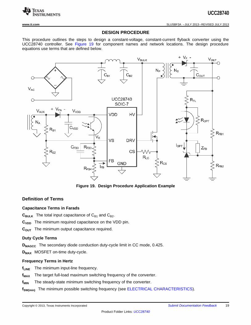
DESIGN PROCEDUREThis procedure outlines the steps to design a constant-voltage, constant-current flyback converter using theUCC28740 controller. See Figure 19 for component names and network locations. The design procedureequations use terms that are defined below.
Figure 19. Design Procedure Application Example
Definition of Terms
Capacitance Terms in FaradsCBULK The total input capacitance of CB1 and CB2.
CVDD The minimum required capacitance on the VDD pin.
COUT The minimum output capacitance required.
Duty Cycle TermsDMAGCC The secondary diode conduction duty-cycle limit in CC mode, 0.425.
DMAX MOSFET on-time duty-cycle.
Frequency Terms in HertzfLINE The minimum input-line frequency.
fMAX The target full-load maximum switching frequency of the converter.
fMIN The steady-state minimum switching frequency of the converter.
fSW(min) The minimum possible switching frequency (see ELECTRICAL CHARACTERISTICS).
Copyright © 2013, Texas Instruments Incorporated Submit Documentation Feedback 19
Product Folder Links: UCC28740
UCC28740
SLUSBF3A –JULY 2013–REVISED JULY 2013 www.ti.com
Current Terms in AmperesIOCC The converter output constant-current target.
IPP(max) The maximum transformer primary peak current.
ISTART The startup bias-supply current (see ELECTRICAL CHARACTERISTICS).
ITRAN The required positive load-step current.
IVSL(run) The VS-pin run current (see ELECTRICAL CHARACTERISTICS).
Current and Voltage Scaling TermsKAM The maximum-to-minimum peak primary current ratio (see ELECTRICAL CHARACTERISTICS).
KLC The current-scaling constant for line compensation(see ELECTRICAL CHARACTERISTICS).
Transformer TermsLP The transformer primary inductance.
NAS The transformer auxiliary-to-secondary turns-ratio.
NPA The transformer primary-to-auxiliary turns-ratio.
NPS The transformer primary-to-secondary turns-ratio.
Power Terms in WattsPIN The converter maximum input power.
POUT The full-load output power of the converter.
PSB The total standby power.
Resistance Terms in OhmsRCS The primary peak-current programming resistance.
RESR The total ESR of the output capacitor(s).
RPL The preload resistance on the output of the converter.
RS1 The high-side VS-pin sense resistance.
RS2 The low-side VS-pin sense resistance.
Timing Terms in SecondstD The total current-sense delay including MOSFET-turnoff delay; add 50 ns to MOSFET delay.
tDM(min) The minimum secondary rectifier conduction time.
tON(min) The minimum MOSFET on time.
tR The resonant frequency during the DCM dead time.
tRESP The maximum response time of the voltage-regulation control-loop to the maximum required load-step.
Voltage Terms in VoltsVBLK The highest bulk-capacitor voltage for standby power measurement.
VBULK(min) The minimum valley voltage on CB1 and CB2 at full power.
VCCR The constant-current regulation factor (see ELECTRICAL CHARACTERISTICS).
VCST(max) The CS-pin maximum current-sense threshold (see ELECTRICAL CHARACTERISTICS).
VCST(min) The CS-pin minimum current-sense threshold (see ELECTRICAL CHARACTERISTICS).
VVDD(off) The UVLO turnoff voltage (see ELECTRICAL CHARACTERISTICS).
20 Submit Documentation Feedback Copyright © 2013, Texas Instruments Incorporated
Product Folder Links: UCC28740
UCC28740
www.ti.com SLUSBF3A –JULY 2013–REVISED JULY 2013
VVDD(on) The UVLO turnon voltage (see ELECTRICAL CHARACTERISTICS).
VDSPK The MOSFET drain-to-source peak voltage at high line.
VF The secondary-rectifier forward-voltage drop at near-zero current.
VFA The auxiliary-rectifier forward-voltage drop.
VLK The estimated leakage-inductance energy reset voltage.
VOΔ The output voltage drop allowed during the load-step transient in CV mode.
VOCBC The target cable-compensation voltage added to VOCV (provided by an external adjustment circuit appliedto the shunt-regulator). Set equal to 0 V if not used.
VOCC The converter lowest output voltage target while in constant-current regulation.
VOCV The regulated output voltage of the converter.
VOV The maximum allowable peak output voltage.
VOVP The overvoltage-detection level at the VS input (see ELECTRICAL CHARACTERISTICS).
VREVA The peak reverse voltage on the auxiliary rectifier.
VREVS The peak reverse voltage on the secondary rectifier.
VRIPPLE The output peak-to-peak ripple voltage at full-load.
AC Voltage Terms in VRMS
VIN(max) The maximum input voltage to the converter.
VIN(min) The minimum input voltage to the converter.
VIN(run) The converter startup (run) input voltage.
Efficiency Termsη The converter overall efficiency at full-power output.
ηSB The estimated efficiency of the converter at no-load condition, excluding startup resistance or bias losses.For a 5-V USB-charger application, 60% to 65% is a good initial estimate.
ηXFMR The transformer primary-to-secondary power-transfer efficiency.
Copyright © 2013, Texas Instruments Incorporated Submit Documentation Feedback 21
Product Folder Links: UCC28740
UCC28740
SLUSBF3A –JULY 2013–REVISED JULY 2013 www.ti.com
Standby Power Estimate and No-Load Switching FrequencyAssuming minimal no-load standby power is a critical design requirement, determine the estimated no-loadpower loss based on an accounting of all no-load operating and leakage currents at their respective voltages.Close attention to detail is necessary to account for all of the sources of leakage, however, in many cases,prototype measurement is the only means to obtain a realistic estimation of total primary and secondary leakagecurrents. At present, converter standby power is certified by compliance-agency authorities based on steady-state room-temperature operation at the highest nominal input voltage rating (typically 230 Vrms).
Equation 6 estimates the standby power loss from the sum of all leakage currents of the primary-sidecomponents of the converter. These leakage currents are measured in aggregate by disconnecting the HV inputof the controller from the bulk-voltage rail to prevent operating currents from interfering with the leakagemeasurement.
(6)
Equation 7 estimates the standby power loss from the sum of all leakage and operating currents of thesecondary-side components on the output of the converter. Leakage currents result from reverse voltage appliedacross the output rectifier and capacitors, while the operating current includes currents required by the shunt-regulator, optocoupler, and associated components.
(7)
Equation 8 estimates the standby power loss from the sum of all leakage and operating currents of the auxiliary-side components on the controller of the converter. Leakage currents of the auxiliary diode and capacitor areusually negligible. The operating current includes the wait-state current, IWAIT, of the UCC28740 controller, plusthe optocoupler-output current for the FB network in the steady-state no-load condition. The VDD voltage in theno-load condition VVDDNL are the lowest practicable value to minimize loss.
(8)
Note that PPRI_SB is the only loss that is not dependent on transformer conversion efficiency. PSEC_SB and PAUX_SBare processed through the transformer and incur additional losses as a consequence. Typically, the transformerno-load conversion efficiency ηSWNL lies in the range of 0.50 to 0.70. Total standby input power (no-loadcondition) is estimated by Equation 9.
(9)
Although the UCC28740 is capable of operating at the minimum switching frequency of 170 Hz, a typicalconverter is likely to require a higher frequency to sustain operation at no-load. An accurate estimate of the no-load switching frequency fSWNL entails a thorough accounting of all switching-related energy losses within theconverter including parasitic elements of the power-train components. In general, fSWNL is likely to lie within therange of 400 Hz to 800 Hz. A more detailed treatment of standby power and no-load frequency is beyond thescope of this data sheet.
Input Bulk Capacitance and Minimum Bulk VoltageDetermine the minimum voltage on the input bulk capacitance, CB1 and CB2 total, in order to determine themaximum Np-to-Ns turns-ratio of the transformer. The input power of the converter based on target full-loadefficiency, the minimum input RMS voltage, and the minimum AC input frequency determine the inputcapacitance requirement.
Maximum input power is determined based on IOCC, VOCV, VCBC (if used), and the full-load conversion-efficiencytarget.
22 Submit Documentation Feedback Copyright © 2013, Texas Instruments Incorporated
Product Folder Links: UCC28740

CCR PSCS XFMR
OCC
V NR
2I
´= ´ h
UCC28740
www.ti.com SLUSBF3A –JULY 2013–REVISED JULY 2013
(10)
Equation 11 provides an accurate solution for the total input capacitance based on a target minimum bulk-capacitor voltage. Alternatively, to target a given input capacitance value, iterate the minimum capacitor voltageto achieve the target capacitance value.
(11)
Transformer Turns-Ratio, Inductance, Primary Peak CurrentThe target maximum switching frequency at full-load, the minimum input-capacitor bulk voltage, and theestimated DCM quasi-resonant time determine the maximum primary-to-secondary turns-ratio of the transformer.
Initially determine the maximum-available total duty-cycle of the on-time and secondary conduction time basedon the target switching frequency, fMAX, and DCM resonant time. For DCM resonant frequency, assume 500 kHzif an estimate from previous designs is not available. At the transition-mode operation limit of DCM, the intervalrequired from the end of secondary current conduction to the first valley of the VDS voltage is ½ of the DCMresonant period (tR), or 1 µs assuming 500 kHz resonant frequency. The maximum allowable MOSFET on-timeDMAX is determined using Equation 12.
(12)
When DMAX is known, the maximum primary-to-secondary turns-ratio is determined with Equation 13. DMAGCC isdefined as the secondary-diode conduction duty-cycle during CC operation and is fixed internally by theUCC28740 at 0.425. The total voltage on the secondary winding must be determined, which is the sum of VOCV,VF, and VOCBC. For the 5-V USB-charger applications, a turns ratio range of 13 to 15 is typically used.
(13)
A higher turns-ratio generally improves efficiency, but may limit operation at low input voltage. Transformerdesign iterations are generally necessary to evaluate system-level performance trade-offs. When the optimumturns-ratio NPS is determined from a detailed transformer design, use this ratio for the following parameters.
The UCC28740 constant-current regulation is achieved by maintaining DMAGCC at the maximum primary peakcurrent setting. The product of DMAGCC and VCST(max) defines a CC-regulating voltage factor VCCR which is usedwith NPS to determine the current-sense resistor value necessary to achieve the regulated CC target, IOCC (seeEquation 14).
Because a small portion of the energy stored in the transformer does not transfer to the output, a transformer-efficiency term is included in the RCS equation. This efficiency number includes the core and winding losses, theleakage-inductance ratio, and a bias-power to maximum-output-power ratio. An overall-transformer efficiency of0.91 is a good estimate based on 3.5% leakage inductance, 5% core & winding loss, and 0.5% bias power, forexample. Adjust these estimates as appropriate based on each specific application.
(14)
The primary transformer inductance is calculated using the standard energy storage equation for flybacktransformers. Primary current, maximum switching frequency, output voltage and current targets, and transformerpower losses are included in Equation 16.
First, determine the transformer primary peak current using Equation 15. Peak primary current is the maximumcurrent-sense threshold divided by the current-sense resistance.
Copyright © 2013, Texas Instruments Incorporated Submit Documentation Feedback 23
Product Folder Links: UCC28740
UCC28740
SLUSBF3A –JULY 2013–REVISED JULY 2013 www.ti.com
(15)
(16)
NAS is determined by the lowest target operating output voltage while in constant-current regulation and by theVDD UVLO turnoff threshold of the UCC28740. Additional energy is supplied to VDD from the transformerleakage-inductance which allows a lower turns ratio to be used in many designs.
(17)
Transformer Parameter VerificationBecause the selected transformer turns-ratio affects the MOSFET VDS and the secondary and auxiliary rectifierreverse voltages, a review of these voltages is important. In addition, internal timing constraints of the UCC28740require a minimum on time of the MOSFET (tON) and a minimum demagnetization time (tDM) of the transformer inthe high-line minimum-load condition. The selection of fMAX, LP, and RCS affects the minimum tON and tDM.
Equation 18 and Equation 19 determine the reverse voltage stresses on the secondary and auxiliary rectifiers.Stray inductance can impress additional voltage spikes upon these stresses and snubbers may be necessary.
(18)
(19)
For the MOSFET VDS peak voltage stress, an estimated leakage inductance voltage spike (VLK) is included.
(20)
Equation 21 determines if tON(min) exceeds the minimum tON target of 280 ns (maximum tCSLEB). Equation 22verifies that tDM(min) exceeds the minimum tDM target of 1.2 µs.
(21)
(22)
VS Resistor Divider, Line CompensationThe VS divider resistors determine the output overvoltage detection point of the flyback converter. The high-sidedivider resistor (RS1) determines the input-line voltage at which the controller enables continuous DRV operation.RS1 is determined based on transformer primary-to-auxiliary turns-ratio and desired input voltage operatingthreshold.
(23)
The low-side VS pin resistor is then selected based on the desired overvoltage limit, VOV.
(24)
24 Submit Documentation Feedback Copyright © 2013, Texas Instruments Incorporated
Product Folder Links: UCC28740
LC S1 CS D PALC
P
K R R t NR
L
´ ´ ´ ´
=
UCC28740
www.ti.com SLUSBF3A –JULY 2013–REVISED JULY 2013
The UCC28740 maintains tight constant-current regulation over varying input line by using the line-compensationfeature. The line-compensation resistor (RLC) value is determined by current flowing in RS1 and the total internalgate-drive and external MOSFET turnoff delay. Assume an internal delay of 50 ns in the UCC28740.
(25)
Output CapacitanceThe output capacitance value is often determined by the transient-response requirement from the no-loadcondition. For example, in typical low-power USB-charger applications, there is a requirement to maintain aminimum transient VO of 4.1 V with a load-step ITRAN from 0 mA to 500 mA. Yet new higher-performanceapplications require smaller transient voltage droop VOΔ with ITRAN of much greater amplitude (such as from no-load to full-load), which drives the need for high-speed opto-coupled voltage feedback.
where• tRESP is the time delay from the moment ITRAN is applied to the moment when IFB falls below 1 µA (26)
Additional considerations for the selection of appropriate output capacitors include ripple-current, ESR, and ESLratings necessary to meet reliability and ripple-voltage requirements. Detailed design criteria for theseconsiderations are beyond the scope of this datasheet.
VDD Capacitance, CVDD
The capacitance on VDD must supply the primary-side operating current used during startup and between low-frequency switching pulses. The largest result of three independent calculations denoted in Equation 27,Equation 28, and Equation 29 determines the value of CVDD.
At startup, when VVDD(on) is reached, CVDD alone supplies the device operating current and MOSFET gate currentuntil the output of the converter reaches the target minimum-operating voltage in CC regulation, VOCC. Now theauxiliary winding sustains VDD for the UCC28740 above UVLO. The total output current available to the load andto charge the output capacitors is the CC-regulation target, IOCC. Equation 27 assumes that all of the outputcurrent of the converter is available to charge the output capacitance until VOCC is achieved. For typicalapplications, Equation 27 includes an estimated qGfSW(max) of average gate-drive current and a 1-V margin addedto VVDD.
(27)
During a worst-case un-load transient event from full-load to no-load, COUT overcharges above the normalregulation level for a duration of tOV, until the output shunt-regulator loading is able to drain VOUT back toregulation. During tOV, the voltage feedback loop and optocoupler are saturated, driving maximum IFB andtemporarily switching at fSW(min). The auxiliary bias current expended during this situation exceeds that normallyrequired during the steady-state no-load condition. Equation 28 calculates the value of CVDD (with a safety factorof 2) required to ride through the tOV duration until steady-state no-load operation is achieved.
(28)
Finally, in the steady-state no-load operating condition, total no-load auxiliary-bias current, IAUXNL is provided bythe converter switching at a no-load frequency, fSWNL, which is generally higher than fSW(min). CVDD is calculated tomaintain a target VDD ripple voltage lower than ΔVVDD, using Equation 29.
Copyright © 2013, Texas Instruments Incorporated Submit Documentation Feedback 25
Product Folder Links: UCC28740

UCC28740
SLUSBF3A –JULY 2013–REVISED JULY 2013 www.ti.com
(29)
Feedback Network BiasingAchieving very low standby power while maintaining high-performance load-step transient response requirescareful design of the feedback network. Optically-coupled secondary-side regulation is used to provide the rapidresponse needed when a heavy load step occurs during the no-load condition. One of the most commonly useddevices to drive the optocoupler is the TL431 shunt-regulator, due to its simplicity, regulation performance, andlow cost. This device requires a minimum bias current of 1 mA to maintain regulation accuracy. Together with theUCC28740 primary-side controller, careful biasing will ensure less than 30 mW of standby power loss at roomtemperature. Where a more stringent standby loss limit of less than 10 mW is required, the TLV431 device isrecommended due to its minimum 80-µA bias capability.
Facilitating these low standby-power targets is the approximate 23-µA range of the FB input for full to no-loadvoltage regulation. The control-law profile graph (see Figure 15) shows that for FB-input current greater than 22µA, no further reduction in switching frequency is possible. Therefore, minimum power is converted at fSW(min).However, the typical minimum steady-state operating frequency tends to be in the range of several-hundredHertz, and consequently the maximum steady-state FB current at no-load will be less than IFBMAX. Even so,prudent design practice dictates that IFBMAX should be used for conservative steady-state biasing calculations. Atthis current level, VFBMAX can be expected at the FB input.
Referring to the Design Procedure Application Example in Figure 19, the main purpose of RFB4 is to speed up theturnoff time of the optocoupler in the case of a heavy load-step transient condition. The value of RFB4 isdetermined empirically due to the variable nature of the specific optocoupler chosen for the design, but tends tofall within the range of 10 kΩ to 100 kΩ. A tradeoff must be made between a lower value for faster transientresponse and a higher value for lower standby power. RFB4 also serves to set a minimum bias current for theoptocoupler and to drain dark current.
It is important to understand the distinction between steady-state no-load bias currents and voltages which affectstandby power, and the varying extremes of these same currents and voltages which affect regulation duringtransient conditions. Design targets for minimum standby loss and maximum transient response often result inconflicting requirements for component values. Trade-offs, such as for RFB4 as discussed previously, must bemade.
During standby operation, the total auxiliary current (used in Equation 8) is the sum of IWAIT into the IC and theno-load optocoupler-output current ICENL. This optocoupler current is given by Equation 30.
(30)
For fast response, the optocoupler-output transistor is biased to minimize the variation of VCE between full-loadand no-load operation. Connecting the emitter directly to the FB input of the UCC28740 is possible, however, anunload-step response may unavoidably drive the optocoupler into saturation which will overload the FB input withfull VDD applied. A series-resistor RFB3 is necessary to limit the current into FB and to avoid excess draining ofCVDD during this type of transient situation. The value of RFB3 is chosen to limit the excess IFB and RFB4 current toan acceptable level when the optocoupler is saturated. Like RFB4, the RFB3 value is also chosen empiricallyduring prototype evaluation to optimize performance based on the conditions present during that situation. Astarting value may be estimated using Equation 31.
(31)
Note that RFB3 is estimated based on the expected no-load VDD voltage, but full-load VDD voltage will be higherresulting in initially higher ICE current during the unload-step transient condition. Because RFB3 is interposedbetween VE and the FB input, the optocoupler transistor VCE varies considerably more as ICE varies and transientresponse time is reduced. Capacitor CFB3 across RFB3 helps to improve the transient response again. The valueof CFB3 is estimated initially by equating the RFB3CFB3 time constant to 1 ms, and later is adjusted higher or lowerfor optimal performance during prototype evaluation.
26 Submit Documentation Feedback Copyright © 2013, Texas Instruments Incorporated
Product Folder Links: UCC28740
UCC28740
www.ti.com SLUSBF3A –JULY 2013–REVISED JULY 2013
The optocoupler transistor-output current ICE is proportional to the optocoupler diode input current by its currenttransfer ratio, CTR. Although many optocouplers are rated with nominal CTR between 50% and 600%, or areranked into narrower ranges, the actual CTR obtained at the low currents used with the UCC28740 falls around5% to 15%. At full-load regulation, when IFB is near zero, VFB is still approximately 0.4 V and this sets a minimumsteady-state current for ICE through RFB4. After choosing an optocoupler, the designer must characterize its CTRover the range of low output currents expected in this application, because optocoupler data sheets rarelyinclude such information. The actual CTR obtained is required to determine the diode input current range at thesecondary-side shunt-regulator.
Referring again to Figure 19, the shunt-regulator (typically a TL431) current must be at least 1 mA even whenalmost no optocoupler diode current flows. Since even a near-zero diode current establishes a forward voltage,ROPT is selected to provide the minimum 1-mA regulator bias current. The optocoupler input diode must becharacterized by the designer to obtain the actual forward voltage versus forward current at the low currentsexpected. At the full-load condition of the converter, IFB is around 0.5 µA, ICE may be around (0.4 V / RFB4), andCTR at this level is about 10%, so the diode current typically falls in the range of 25 µA to 100 µA. Typical opto-diode forward voltage at this level is about 0.97 V which is applied across ROPT. If ROPT is set equal to 1 kΩ, thisprovides 970 µA plus the diode current for IOPT.
As output load decreases, the voltage across the shunt-regulator also decreases to increase the current throughthe optocoupler diode. This increases the diode forward voltage across ROPT. CTR at no-load (when ICE ishigher) is generally a few percent higher than CTR at full-load (when ICE is lower). At steady-state no-loadcondition, the shunt-regulator current is maximized and can be estimated by Equation 30 and Equation 32.IOPTNL, plus the sum of the leakage currents of all the components on the output of the converter, constitute thetotal current required for use in Equation 7 to estimate secondary-side standby loss.
(32)
The shunt-regulator voltage can decrease to a minimum, saturated level of about 2 V. To prevent excessivediode current, a series resistor, RTL, is added to limit IOPT to the maximum value necessary for regulation.Equation 33 provides an estimated initial value for RTL, which may be adjusted for optimal limiting later during theprototype evaluation process.
(33)
The output-voltage sense-network resistors RFB1 and RFB2 are calculated in the usual manner based on theshunt-regulator reference voltage and input bias current. Having characterized the optocoupler at low currentsand determined the initial values of RFB1, RFB2, RFB3, RFB4, CFB3, ROPT and RTL using the above procedure, theDC-bias states of the feedback network can be established for steady-state full-load and no-load conditions.Adjustments of these initial values may be necessary to accommodate variations of the UCC28740, optocoupler,and shunt-regulator parameters for optimal overall performance.
The shunt-regulator compensation network, ZFB, is determined using well-established design techniques forcontrol-loop stability. Typically, a type-II compensation network is used. The compensation design procedure isbeyond the scope of this datasheet.
REVISION HISTORY
Changes from Original (July, 2013) to Revision A Page
• Changed marketing status from Product Preview to Production Data. ................................................................................ 1
Copyright © 2013, Texas Instruments Incorporated Submit Documentation Feedback 27
Product Folder Links: UCC28740
PACKAGE OPTION ADDENDUM
www.ti.com 27-Jul-2013
Addendum-Page 1
PACKAGING INFORMATION
Orderable Device Status(1)
Package Type PackageDrawing
Pins PackageQty
Eco Plan(2)
Lead/Ball Finish MSL Peak Temp(3)
Op Temp (°C) Device Marking(4/5)
Samples
UCC28740D ACTIVE SOIC D 7 75 Green (RoHS& no Sb/Br)
CU NIPDAU Level-1-260C-UNLIM -40 to 125 U28740
UCC28740DR ACTIVE SOIC D 7 2500 Green (RoHS& no Sb/Br)
CU NIPDAU Level-1-260C-UNLIM -40 to 125 U28740
(1) The marketing status values are defined as follows:ACTIVE: Product device recommended for new designs.LIFEBUY: TI has announced that the device will be discontinued, and a lifetime-buy period is in effect.NRND: Not recommended for new designs. Device is in production to support existing customers, but TI does not recommend using this part in a new design.PREVIEW: Device has been announced but is not in production. Samples may or may not be available.OBSOLETE: TI has discontinued the production of the device.
(2) Eco Plan - The planned eco-friendly classification: Pb-Free (RoHS), Pb-Free (RoHS Exempt), or Green (RoHS & no Sb/Br) - please check http://www.ti.com/productcontent for the latest availabilityinformation and additional product content details.TBD: The Pb-Free/Green conversion plan has not been defined.Pb-Free (RoHS): TI's terms "Lead-Free" or "Pb-Free" mean semiconductor products that are compatible with the current RoHS requirements for all 6 substances, including the requirement thatlead not exceed 0.1% by weight in homogeneous materials. Where designed to be soldered at high temperatures, TI Pb-Free products are suitable for use in specified lead-free processes.Pb-Free (RoHS Exempt): This component has a RoHS exemption for either 1) lead-based flip-chip solder bumps used between the die and package, or 2) lead-based die adhesive used betweenthe die and leadframe. The component is otherwise considered Pb-Free (RoHS compatible) as defined above.Green (RoHS & no Sb/Br): TI defines "Green" to mean Pb-Free (RoHS compatible), and free of Bromine (Br) and Antimony (Sb) based flame retardants (Br or Sb do not exceed 0.1% by weightin homogeneous material)
(3) MSL, Peak Temp. -- The Moisture Sensitivity Level rating according to the JEDEC industry standard classifications, and peak solder temperature.
(4) There may be additional marking, which relates to the logo, the lot trace code information, or the environmental category on the device.
(5) Multiple Device Markings will be inside parentheses. Only one Device Marking contained in parentheses and separated by a "~" will appear on a device. If a line is indented then it is a continuationof the previous line and the two combined represent the entire Device Marking for that device.
Important Information and Disclaimer:The information provided on this page represents TI's knowledge and belief as of the date that it is provided. TI bases its knowledge and belief on informationprovided by third parties, and makes no representation or warranty as to the accuracy of such information. Efforts are underway to better integrate information from third parties. TI has taken andcontinues to take reasonable steps to provide representative and accurate information but may not have conducted destructive testing or chemical analysis on incoming materials and chemicals.TI and TI suppliers consider certain information to be proprietary, and thus CAS numbers and other limited information may not be available for release.
In no event shall TI's liability arising out of such information exceed the total purchase price of the TI part(s) at issue in this document sold by TI to Customer on an annual basis.
TAPE AND REEL INFORMATION
*All dimensions are nominal
Device PackageType
PackageDrawing
Pins SPQ ReelDiameter
(mm)
ReelWidth
W1 (mm)
A0(mm)
B0(mm)
K0(mm)
P1(mm)
W(mm)
Pin1Quadrant
UCC28740DR SOIC D 7 2500 330.0 12.4 6.4 5.2 2.1 8.0 12.0 Q1
PACKAGE MATERIALS INFORMATION
www.ti.com 24-Jul-2013
Pack Materials-Page 1

*All dimensions are nominal
Device Package Type Package Drawing Pins SPQ Length (mm) Width (mm) Height (mm)
UCC28740DR SOIC D 7 2500 367.0 367.0 35.0
PACKAGE MATERIALS INFORMATION
www.ti.com 24-Jul-2013
Pack Materials-Page 2
IMPORTANT NOTICE
Texas Instruments Incorporated and its subsidiaries (TI) reserve the right to make corrections, enhancements, improvements and otherchanges to its semiconductor products and services per JESD46, latest issue, and to discontinue any product or service per JESD48, latestissue. Buyers should obtain the latest relevant information before placing orders and should verify that such information is current andcomplete. All semiconductor products (also referred to herein as “components”) are sold subject to TI’s terms and conditions of salesupplied at the time of order acknowledgment.
TI warrants performance of its components to the specifications applicable at the time of sale, in accordance with the warranty in TI’s termsand conditions of sale of semiconductor products. Testing and other quality control techniques are used to the extent TI deems necessaryto support this warranty. Except where mandated by applicable law, testing of all parameters of each component is not necessarilyperformed.
TI assumes no liability for applications assistance or the design of Buyers’ products. Buyers are responsible for their products andapplications using TI components. To minimize the risks associated with Buyers’ products and applications, Buyers should provideadequate design and operating safeguards.
TI does not warrant or represent that any license, either express or implied, is granted under any patent right, copyright, mask work right, orother intellectual property right relating to any combination, machine, or process in which TI components or services are used. Informationpublished by TI regarding third-party products or services does not constitute a license to use such products or services or a warranty orendorsement thereof. Use of such information may require a license from a third party under the patents or other intellectual property of thethird party, or a license from TI under the patents or other intellectual property of TI.
Reproduction of significant portions of TI information in TI data books or data sheets is permissible only if reproduction is without alterationand is accompanied by all associated warranties, conditions, limitations, and notices. TI is not responsible or liable for such altereddocumentation. Information of third parties may be subject to additional restrictions.
Resale of TI components or services with statements different from or beyond the parameters stated by TI for that component or servicevoids all express and any implied warranties for the associated TI component or service and is an unfair and deceptive business practice.TI is not responsible or liable for any such statements.
Buyer acknowledges and agrees that it is solely responsible for compliance with all legal, regulatory and safety-related requirementsconcerning its products, and any use of TI components in its applications, notwithstanding any applications-related information or supportthat may be provided by TI. Buyer represents and agrees that it has all the necessary expertise to create and implement safeguards whichanticipate dangerous consequences of failures, monitor failures and their consequences, lessen the likelihood of failures that might causeharm and take appropriate remedial actions. Buyer will fully indemnify TI and its representatives against any damages arising out of the useof any TI components in safety-critical applications.
In some cases, TI components may be promoted specifically to facilitate safety-related applications. With such components, TI’s goal is tohelp enable customers to design and create their own end-product solutions that meet applicable functional safety standards andrequirements. Nonetheless, such components are subject to these terms.
No TI components are authorized for use in FDA Class III (or similar life-critical medical equipment) unless authorized officers of the partieshave executed a special agreement specifically governing such use.
Only those TI components which TI has specifically designated as military grade or “enhanced plastic” are designed and intended for use inmilitary/aerospace applications or environments. Buyer acknowledges and agrees that any military or aerospace use of TI componentswhich have not been so designated is solely at the Buyer's risk, and that Buyer is solely responsible for compliance with all legal andregulatory requirements in connection with such use.
TI has specifically designated certain components as meeting ISO/TS16949 requirements, mainly for automotive use. In any case of use ofnon-designated products, TI will not be responsible for any failure to meet ISO/TS16949.
Products Applications
Audio www.ti.com/audio Automotive and Transportation www.ti.com/automotive
Amplifiers amplifier.ti.com Communications and Telecom www.ti.com/communications
Data Converters dataconverter.ti.com Computers and Peripherals www.ti.com/computers
DLP® Products www.dlp.com Consumer Electronics www.ti.com/consumer-apps
DSP dsp.ti.com Energy and Lighting www.ti.com/energy
Clocks and Timers www.ti.com/clocks Industrial www.ti.com/industrial
Interface interface.ti.com Medical www.ti.com/medical
Logic logic.ti.com Security www.ti.com/security
Power Mgmt power.ti.com Space, Avionics and Defense www.ti.com/space-avionics-defense
Microcontrollers microcontroller.ti.com Video and Imaging www.ti.com/video
RFID www.ti-rfid.com
OMAP Applications Processors www.ti.com/omap TI E2E Community e2e.ti.com
Wireless Connectivity www.ti.com/wirelessconnectivity
Mailing Address: Texas Instruments, Post Office Box 655303, Dallas, Texas 75265Copyright © 2013, Texas Instruments Incorporated