
A conceptual instrument to measure the success of branding ...

LBNL-39018 UC-404
ERNEST DRLANDD LAWRENCE BERKELEY NATIONAL LABORATORY
Conceptual Design of a Novel Instrument for Producing Intense Pulses of 10 ps X-rays for Ultra-Fast Fluorescence Measurements
G.J. Gruber Life Sciences Division
May 1996 Master's Project Report
"BUTTON OF THIS DOCUMENT IS UNMTED^ M A S T E R
RECEIVED m 2 0 B96
OSTl

DISCLAIMER
This document was prepared as an account of work sponsored by the United States Government. While this document is believed to contain correct information, neither the United States Government nor any agency thereof, nor The Regents of the University of California, nor any of their employees, makes any warranty, express or implied, or assumes any legal responsibility for the accuracy, completeness, or usefulness of any information, apparatus, product, or process disclosed, or represents that its use would not infringe privately owned rights. Reference herein to any specific commercial product, process, or service by its trade name, trademark, manufacturer, or otherwise, does not necessarily constitute or imply its endorsement, recommendation, or favoring by the United States Government or any agency thereof, or The Regents of the University of California. The views and opinions of authors expressed herein do not necessarily state or reflect those of the United States Government or any agency thereof, or The Regents of the University of California.
Ernest Orlando Lawrence Berkeley National Laboratory is an equal opportunity employer.

DISCLAIMER
Portions of this document may be illegible in electronic image products. Images are produced from the best available original document.


LBNL-39018 UC-404
Conceptual Design of a Novel Instrument for Producing Intense Pulses of 10 ps X-rays for Ultra-Fast Fluorescence Measurements
Gregory J. Gruber Master's Project Report
Department of Electrical Engineering and Computer Science University of California, Berkeley
and
Life Sciences Division Ernest Orlando Lawrence Berkeley National Laboratory
University of California Berkeley, CA 94720
May 1996
This work was supported by the Fannie and John Hertz Foundation and by the Director, Office of Energy Research, Office of Basic Energy Sciences, Materials Sciences Division, of the U.S. Department of Energy under Contract No. DE-AC03-76SF00098.

ACKNOWLEDGMENTS
I wish to thank my research advisor, Dr. Stephen Derenzo, for his support and guidance as I worked toward completion of this degree, and most especially for his contributions to this report. I further wish to thank Dr. William Moses for the helpful discussions he provided and the rest of the Center for Functional Imaging personnel for the support and assistance they offered. In addition, I thank Dr. David Attwood for agreeing to be the second reader for this report and for enduring my hectic schedule near the time of its completion.
I am indebted to my family members for their constant and unfaltering support, and especially to my parents for the guidance and encouragement they have provided throughout my life. I also thank the friends who have stood with me through the good times and the bad, helping make it possible for me to complete this work.
Finally, throughout most of my work on this project I have been financially supported by the Fannie and John Hertz Foundation. I am extremely grateful for this fellowship support, as it has made this research possible and has contributed greatly to my graduate education in general. My work was also supported by the Director, Office of Energy Research, Office of Basic Energy Sciences, Materials Sciences Division, of the U.S. Department of Energy under Contract No. DE-AC03-76SF00098, which provided me with access to the National Energy Research Supercomputing Center (NERSC) so that I could conduct EGUN simulations.
page 2

ABSTRACT
A novel bench-top device for producing intense, fast pulses of x-rays has been designed with 10 ps fwhm (full-width at half-maximum) x-ray pulse width, 120 keV maximum energy, 100 kHz repetition rate, and 1 A peak current onto the x-ray anode. The device includes three sections: (1) an electron gun that generates 5 ns wide pulses of 120 keV electrons at 100 kHz; (2) solenoidal magnetic lenses and deflection plates that focus the electrons onto an aperture plate and sweep the pulsed beam past the aperture, respectively; and (3) a tungsten anode onto which the post-aperture electrons are focused, producing pulses of x-rays. At a sweeping rate of 1013 V/s, the electron pulses and resulting x-ray pulses are reduced to about 10 ps. The design process used EGUN (an electron optics and gun design program) electron trajectory simulations, including calculation of important space charge effects. When built, this instrument will be used to excite new, fast, bright scintillator samples in crystal or powdered form, allowing fluorescent lifetimes and spectra to be measured with a microchannel PMT. The very narrow 10 ps x-ray pulse width is necessary for accurate measurements of the risetimes of very fast scintillators (e.g., BaF^. In addition, the large x-ray flux (1 A peak current) is advantageous when using a reflection grating monochromator to measure decay times at different wavelengths.
1.0 INTRODUCTION AND MOTIVATION
The performance of PET (positron emission tomography) instrumentation depends heavily on the scintillator crystals used as detectors. Faster and brighter scintillators could represent improvements both in detector recovery time and in the ability to reject radiation resulting from Compton scattering within the patient and could potentially even reduce detector cost. The search for new scintillators requires a means of exciting samples so that fluorescent lifetimes and spectra can be measured. Previous efforts to find better scintillators made use of an electron synchrotron in single-bunch mode to measure the x-ray excited fluorescence of over 400 compounds [1, 2], a process that was both expensive and time-consuming. More recently, a table-top device capable of producing 109 ps fwhm pulses of x-rays has been used in the search for new scintillators [3, 4]. While this instrument has reduced the cost and increased the ease of making scintillation measurements, it generates peak currents of only 1 mA and produces x-rays with a maximum energy of 30 keV. Hence, the 10 ps x-ray pulse width, 1 A peak current, 120 keV maximum x-ray photon energy design presented in this report represents a major improvement
Narrow x-ray pulse widths, even down to a resolution of 10 ps, are necessary to accurately measure the risetimes of some very fast self-activated scintillators (e.g., BaF2). High x-ray photon flux (i.e., 1 A peak current onto the x-ray anode) results in more energy being delivered to the scintillator sample and hence more light output generated by the sample, providing for scintillation measurements with a greater S/N ratio. Finally, x-rays with energies up to 120 keV are desirable for three significant reasons: (1) higher energy x-rays deliver more energy to the scintillator sample, providing the same benefit as does increased x-ray flux; (2) the ratio of x-rays absorbed in the sample to x-rays absorbed in the sample's quartz cuvette is greater for higher energy x-rays; and (3) at energies near 120 keV non-scintillation materials with high indices of refraction will produce a small amount of Cerenkov light, a phenomenon that can be used to accurately measure the impulse response of the instrumentation system.
The use of deflection systems to chop electron beams to pulses of the order of 10 ps duration has been reported in numerous articles [5-7], though these are generally oriented toward scanning electron microscope (SEM) applications. As such, the beam currents are typically less than 1 nA, meaning that space charge effects can be essentially ignored and that focal spot sizes are tens of |im in diameter. Beam focusing is thus simpler in that space charge repulsion is not dominant, and beam sweeping via deflection plates is less
page 3

complicated because the small spot sizes mean that lesser sweep speeds are required to chop the electron pulses to 10 ps. In the design of this pulsed x-ray instrument, however, both of these concerns proved challenging. Conversely, the energy spread of the chopped beam is of significant concern in SEM, something that is not true for scintillation measurement applications.
In addition to the goals of a 1 A beam and 10 ps x-ray pulse widths, the chief design criteria were table-top size, low cost, and the ability to observe scintillation behavior in both powders and crystals. Sweeping the pulsed electron beam past an aperture to limit the duration of the pulses makes the pulse width goal achievable in a relatively low cost, table-top instrument. The use of solenoidal magnetic lenses makes it possible to contain the electron pulses despite space charge effects, allowing for a 1 A impact beam on the x-ray anode. The remainder of this report discusses the design of the pulsed x-ray instrument, explains the reasoning behind and the tradeoffs associated with the decisions that have been made, and presents electron trajectory simulations that help characterize the instrument's predicted performance.
2.0 GENERAL DESIGN OVERVIEW
2.1 Section 1: Electron Gun
The pulsed x-ray source consists of three sections, as shown diagramatically in Figure 1. The first stage is an electron gun in which a beam of electrons is generated via thermionic emission by heating a 1 cm2 metal surface (the cathode). A grid pulsed between -400 V and +400 V is capable of completely turning off the electron beam and is used to limit the length of individual electron pulses to approximately 5 ns. The electrons are accelerated across 120 kV, and the metal walls surrounding the beam act as an electrostatic lens that, with the help of a solenoidal magnetic lens, focuses the electrons enough to counteract space charge repulsion and yield a nearly parallel beam of electrons upon exit from the first section. The ultimate repetition rate of the x-ray pulses is set by the rate at which the cathode grid is pulsed and has a maximum frequency of 100 kHz. The cost of this section is estimated at approximately $100,000 [8].
First Section Second Section Third Section
Figure 1. The three sections of the pulsed x-ray instrument, most of which is cylindrically symmetric. The instrument as shown is approximately 0.7 m long and has a radius of about 0.1 m.
page 4

2.2 Section 2: Deflection System, Magnetic Lenses, and Aperture Plate
The second stage consists of three main components: solenoidal magnetic lenses, a pair of deflection plates, and a plate with a 0.32 mm diameter aperture. Focusing of the pulsed electron beam onto the aperture is achieved by running current in a solenoid around the instrument (i.e., outside of the vacuum) at densities as great as 150 A«turns/cm2, forming a magnetic field that forces the electrons to converge to a spot size diameter of about 0.32 mm despite space charge repulsion. The deflection plates, located within the weaker section of the magnetic lens system that maintains the parallel nature of the beam rather than focusing it to a spot, uses two charged metallic plates to form an electric field that deflects the electron beam. The lower plate is held at ground potential, while the upper one is modulated via a high power triode (e.g., CPI, Eimac Division model 3CPX5000A7, cost of $2600) at an amplitude of 16 kV and a frequency of 100 MHz, providing for a maximum sweep rate of about 1013 V/s. The system is synchronized such that when each pulse of electrons traverses the space between the deflection plates, the upper plate is brought to ground potential exactly once, always moving from positive to negative voltage. Hence during this zero-crossing the electron beam is swept from above the aperture to below it, spending about 10 ps actually passing through the aperture. The remainder of the beam is absorbed by the aperture plate, dissipated primarily as heat
2.3 Section 3: Tungsten Anode, Magnetic Lenses, and Exit Window
The third stage involves additional magnetic lenses and a tungsten anode (at ground potential). Once again current running in a solenoid around the instrument forms a magnetic lens system that focuses the electron beam to a diameter of about 0.45 mm, this time onto the tungsten anode. The 10 ps electron pulses thus collide with the tungsten anode over a relatively small area, in the process generating x-rays with energies up to 120 keV. These x-rays exit the instrument through a beryllium window and are then filtered by an aluminum plate that attenuates lower-energy photons, especially those below 7 keV. Space near the exit window must be left for a sample, which is to be contained within a quartz cuvette.
2.4 EGUN Electron Trajectory Simulations
Designing the metal wall geometries and the magnetic lenses for minimal focal spot sizes required careful simulation of the electron trajectories. To this end EGUN, an electron optics and gun design program written by W. B. Herrmannsfeldt [9] was used. The program computes the trajectories of charged particles through electrostatic and magnetostatic fields, accounting for space charge repulsion, self-magnetic fields, relativistic effects, and space-charge-limited emission from the cathode surface (i.e., Child-Langmuir equation). The code is 2-D for all fields and 3-D for all particle motion, making cylindrical symmetry the best choice for this application. User-input boundary values, both Dirichlet (on which the potential is known) and Neumann (on which the normal derivative of the potential is known), are thus defined in terms of radial and z-axis coordinates. EGUN uses these boundary conditions and finite difference equations to solve Poisson's equation, then differentiates the resulting potential distribution to determine the electric field. In addition, magnetic field effects may be included by defining the location and current magnitude (in A»turns) of a series of circular coils, allowing for simulation of solenoidal magnetic lenses.
2.5 Safety Concerns
It is obvious that this pulsed x-ray instrument is a source of ionizing radiation that could prove harmful to the instrument operators), so shielding must be provided to attenuate x-rays emanating from both the tungsten anode and the wall locations in the second stage where the 120 keV electrons impact. Comprehensive safety measures (e.g., an interlock
page 5

circuit) must be included such that no single point failure in the system is capable of causing the operators) to undergo x-ray exposure.
An additional safety concern is the fact that the cathode and grid assembly are at a potentially dangerous voltage of -120 kV. A safety cage and interlock system (less than 1 m A current, less than 5 J energy storage) must surround this section of the instrument so that the operator(s) is protected from discharge.
3.0 MAJOR DESIGN TRADEOFFS/LIMITATIONS
3.1 General Focusing Considerations
The limitations inherent in focusing a 1A electron beam to a small spot in the presence of significant space charge repulsion have a critical influence on the design of this instrument As will be addressed in detail later, a smaller spot size provides for a shorter time duration for the pulses emerging from the aperture. Given the challenges associated with chopping pulses down to 10 ps, it is thus critical to make the focal spot size on the aperture plate as small as is reasonably possible. Additionally, a small spot size on the anode is desirable in order "to approximate an x-ray point source and prevent x-ray time-of-flight differences from opposite sides of the anode spot from seriously degrading x-ray pulse time resolution.
Three of the most important factors that affect beam focusing and the smallest achievable spot size are: acceleration voltage, beam current, and lens characteristics/geometry. As for the latter, solenoidal magnetic lenses were chosen over electrostatic lenses because magnetic lens aberrations are generally less dominant and, since magnetic lenses are located outside of the beam vacuum, they are more convenient and simpler to use. The one exception to this is in the electron gun, where an electrostatic lens used to maintain the parallel nature of the beam is formed by properly shaping the gun's metal walls. Little complexity is added by incorporating this lens into the instrument, as those walls must in any case present a voltage differential of 120 kV in order to accelerate the electrons emerging from the cathode.
Greater current density in the magnetic lens provides for stronger focusing ability, which is important given the significant space charge repulsion of a 1 A beam. However, in most magnetic lenses heat dissipation concerns limit this density to around 150 A^turns/cm2
[10]. Even then a combination of epoxy poured over and between the coils (to increase thermal conductivity) and/or water cooling must be employed.
Both current and voltage have important and complicated influences on the focal spot diameter of an electron beam. With attention to space charge repulsion, El-Kareh [11] calculates the theoretical minimum beam radius as
rm = ri«exp[-'D»vi
2»^»e»me/(I»qe)], (eq. 1)
where rm is the rninimum beam radius, r; is the initial beam radius upon entering the lens, x> is the beam velocity, I is the beam current, and v{ is the inward radial component of the electron velocities at the outer surface of the beam. This equation, however, involves the assumption that upon exiting the lens (e.g., the electric field of an electrostatic lens) the radial components of the electron velocities are proportional to their distances from the beam axis. This thus assumes an ideal lens free from aberrations, as well as a lens with a relatively short length in the direction of the beam motion. Lens aberrations, however, cannot be ignored, and the use of long, solenoidal magnetic lenses contradicts the assumption as to the lens' range of effect Thus while this equation is inadequate for our purposes, it does begin to demonstrate the strong dependency that spot size has on beam current and the acceleration voltage, V. Note that the square root of V, ignoring relativistic effects, is proportional to D, which under the ideal lens assumption is in turn proportional to Vj. This then means that to first approximation the exponential power contains the term V3/2/I.
page 6

Figure 2 displays EGUN simulation results for the focusing of an initially parallel beam with a solenoidal magnetic lens that has been configured to work well with 1 A beams. The curves characterize the dependence of the focal spot diameter on the beam current and acceleration voltage. At low currents the spot diameter is limited by the nature of the lens system, including aberrations, though smaller spot sizes could be achieved were the lens system tailored to smaller currents. For large currents space charge repulsion rapidly increases spot size, demonstrating a near-exponential dependence. Smaller spot diameters tend to be achieved with greater acceleration voltages because the beam travels faster and hence space charge has less time to increase beam size. However, while smaller spot sizes are achievable using acceleration voltages greater than 120 kV, x-ray energies above 120 keV are undesirable in scinitillation measurements because excessive Cerenkov light will be produced in the sample compounds, obscuring the scintillation responses.
Current (A)
Figure 2. Focal spot diameter versus beam current for electron beam energies of 40 keV and 120 keV, as computed using EGUN. Simulations assumed an initially parallel beam of radius 5.6 mm focused by a solenoidal magnetic lens with an inner radius of 10 mm and a current density of 150 A»turns/cm2. No 40 keV data are presented above 5 A because the beam began striking the solenoid walls before being brought to a focus.
3.2 Cathode Grid
A fine wire mesh grid located a short distance in front of the metal cathode provides a means of controlling the beam current. By pulsing the grid voltage appropriately, it is possible to vary the current coming off of the cathode, allowing it to swing between a peak current level and zero. When the grid is held at a negative bias relative to the cathode, the resulting electric field repels electrons and retards thermionic emission, thereby decreasing the cathode-to-anode current. When the bias is strong enough, such a grid can effectively halt electron emission, decreasing the current to nearly zero. Similarly, driving the grid positive with respect to the cathode provides an electric field that serves to pull electrons from the cathode, stimulating emission and increasing current generation. To avoid negatively affecting the equipotential lines established by the walls of the electron gun, it is desirable to place and shape the grid such that it is falls along the equipotential line equal to the grid's positive drive voltage.
Cathode grids present several other potential complications that must be considered. Such a grid will intercept around 10% of the current emanating from the cathode [12], with increasingly higher intercept percentages the more positive the grid is driven. If the grid's mesh size is large compared to the grid-to-cathode spacing, its control characteristics become
page 7

more complicated and cannot be modeled as accurately. Further, if the grid is placed too close to the cathode, heat radiated from the cathode can cause the grid temperature to rise to the point where it, too, emits electrons. Finally, lead inductances within the gun can yield a positive feedback situation in which oscillations or bistable current outputs will result for some drive levels [12].
In the case of a 1 cm2 cathode with a 1A peak current, a grid cutoff voltage near -400 V and a peak drive voltage near 4400 V would be reasonable, as would the 1 mm cathode-to-grid spacing used in [12]. By driving the grid to the required biases with a high-frequency voltage pulser, 5 ns pulse widths are commonly achieved (pulse widths as small as 1 ns are not uncommon). The capacitive, highly nonlinear nature of the grid impedance, however, makes driving the grid with high-frequency pulses tricky and requires careful design of the pulser electronics [8].
3.3 Sweeping the Electron Beam with Deflection Plates
Sweeping the pulsed electron beam past the aperture is to be accomplished by rapidly varying the voltage on one deflection plate while the second plate is held at a constant potential. This process is displayed in Figure 3 for the case in which the bottom plate is grounded and the voltage on die upper plate experiences sinusoidal modulation.
pulsed electron beam
max
aperture diameter
w
Figure 3. Pulsed electron beam swept past the aperture by deflection plates, thereby reducing the time duration of the post-aperture electron pulses.
The following parameters related to Figure 3 are used below in a series of equations detailing the electron chopping process:
vy(t) y(t) w L
dmax dap
initial horizontal velocity of beam vertical velocity of beam vertical deflection distance of beam (t and x are linearly related) length of deflection plates distance from edge of deflection plates to aperture plate vertical distance from aperture to beam impact point vertical distance from aperture to beam impact point at maximum deflection diameter of aperture distance between deflection places
page 8

A = area of deflection plates C = capacitance of deflection plates E = electric field between deflection plates V = voltage difference across deflection plates
The deflection plates are assumed to be a parallel plate capacitor with a uniform electric field given by: E = V/dpl. Thus, for a given value of the electric field, E, the vertical deflection of the electrons while they are still between the deflection plates (0 < x < w) is given by
y(t)=-qe-E«t2/2me. (eq. 2)
The time the electrons spend traversing the space between the deflection plates is: w/V;. Hence, upon emerging from the deflection plates (x = w), the electrons have undergone a vertical deflection of
y(t = w/Vi) = qe»E«(w/Vi)2/2me (eq. 3)
and achieved an upward velocity of
vy(t = w/V;) = qe»E»(w/Vi) / me. (eq. 4)
After emerging from between the deflection plates, the electrons continue on to the aperture plate (x = w + L) over an additional period of time given by L/Vj. During this time (w/V; < t < (w + L)/V;) the vertical deflection of the electron beam is defined by
y(t) = qe»E«(w/Vj)2 / 2me + (t - w/V;>qe»E«(w/V;) / me. (eq. 5)
Thus, upon impact with the aperture plate the electrons will have a deflection distance from the center of the aperture of
d i m = y(t=(w + L)/vi) = w(w/2 + L>qe-E/(me«vi
2). (eq. 6)
Sweeping the electrons downward across the aperture plate is performed by rapidly decreasing the voltage on the upper deflection plate, thereby causing the electric field between the plates to change quickly. The sweeping speed (vertical distance per time) of the electron beam is
d(dim)/dt = (dE/dt)-w(w/2 + L)«qe / (me«Vi
2). (eq. 7)
The only sweeping speed of interest is that when the beam is crossing the aperture, the duration of which is brief enough that it can safely be assumed that dE/dt has a constant value. Further, because the deflection plates form a parallel plate capacitor, the dV/dt corresponding to the value of dE/dt in question is approximately given by d fdE/dt.
The time required to sweep the electron beam past an aperture of size d (i.e., the beam travels a vertical distance equal to d^) is
time resolution = d^ / [d(dim)/dt] = d^»dp]«me»v2 / [(dV/dt)»w(w/2 + L)«qJ. (eq. 8)
Time resolution defines the pulse width of the electron bunches emerging from the aperture, thereby indicating the minimum possible time during which a given electron pulse will impact upon the anode.
The design challenge of achieving 10 ps wide x-ray pulses thus involves consideration of the numerous factors, some with complex interrelations, illustrated in equation 8. To
page 9

minimize the time resolution it is desirable to make the distance between the deflection plates (dpl) small but their length (w) long. However, the constraint of not having the deflection plates intercept the beam, even at maximum deflection, places limits on these values. Increasing the plates-to-aperture distance (L) is also attractive, and indeed this was done as much as possible, but L is limited in that the farther the beam travels before being brought to a focus, the less uniform the current distribution becomes and the greater the resulting focal spot diameter.
This then leaves the aperture diameter (d^) and the deflection plate sweeping rate (dV/dt) to be minimized and maximized, respectively. The former is obviously limited by lens aberrations and space charge repulsion, while the latter is limited by voltage switching technology.
With attention to these effects, the following geometry was used in the final instrument design:
d^ = 0.32 mm dpl = 35 mm w = 100 mm L = 178 mm
For this geometry and electron energies of 120 keV (i.e., relativistic velocity of v ; = 0.5867c), the dV/dt required to achieve a post-aperture electron pulse time resolution of 10 ps is 8.64»1012 V/s.
3.4 Anode Angle
The electron beam is swept by the deflection plates such that, once near the aperture, it traverses a distance equal to the aperture diameter in approximately 10 ps. The electron beam at this point has been focused to a spot size equal to the diameter of the aperture, meaning that electrons will actually pass through the aperture for a period of about 20 ps. The 2-D shape of the electron pulse emerging from the aperture will approximately be a parallelogram, with the vertical height equal to the aperture size (0.32 mm) and the length of each horizontal line equal to the distance that the electrons travel in 10 ps (1.76 mm at 120 keV). The process of forming an electron pulse is summarized in Figure 4.
TIME = 0 TIME = 10 ps TIME = 20ps
pulsed electron beam
sweeping action ,
aperture
1.76 mm i 1
chopped electron pulse
Figure 4. Formation of a post-aperture electron pulse via beam chopping. The resulting pulse will initially have a parallelogram-type shape, the dimensions of which depend on the accelerating voltage and the aperture diameter.
page 10

Pulses emerging from the aperture will demonstrate an angle (from the horizontal) of tan"1 (0.32 mm / 1.76 mm) = 10.3°. If the anode were at this same angle, then the electrons in the leading edge of the parallelogram would all strike the anode simultaneously. This would lead to an x-ray pulse width of about 10 ps, as all of the electrons would impact with the anode within a period of 10 ps. If, however, the anode were at a greater angle (e.g., 45°), the upper portion of the pulse would strike the anode before the lower portion, and the resulting pulse of x-rays would be spread out over a greater period of time (Figure 5).
first electrons to impact
Figure 5. Geometry of electron pulse impact at the anode, assuming that the parallelogram shape is maintained after emergence from the aperture. The length of 1.76 mm assumes an electron velocity of 0.5867c imparted by 120 kV acceleration.
Assuming that the electrons have been accelerated through 120 kV, the time period over which a single pulse will impact on the anode is given by:
impact time = [2(1.76 mm)-d^/tancj)]/(0.5867c), 0<(()< 90° (eq. 9)
In the case of a 45° anode angle and an aperture diameter of 0.32 mm, a pulse would impact with the anode over a period of 18.2 ps. This is nearly double the 10 ps time resolution achieved at the aperture, demonstrating the importance of choosing the anode angle wisely.
These considerations assume that the parallelogram shape of the electron pulse will be maintained as it travels from the aperture to the anode. In reality, the electrons will initially diverge due to space charge effects and then again be focused to a spot by magnetic lenses. Because of the asymmetries inherent in the parallelogram shape of the electron pulse, this divergence and re-focusing will significantly alter its shape. What is important, then, is not to try to determine the optimal anode angle, since that would be exceedingly difficult to do given simulation limitations, but rather to allow the anode angle to be easily physically altered so that adjustments can be made once the instrument is built. By using Cerenkov light to measure the impulse response of the instrument, it would be a relatively simple matter to adjust the anode angle until the minimum duration fwhm impulse response were achieved.
It is also clear from these considerations that in order to achieve the minimum total electron-anode impact time, the deflection plates must always sweep the electron pulses in the same direction. In Figures 4 and 5 this has arbitrarily been assigned to be downward. Were sweeping past the aperture occasionally done in the opposite, upward direction, the lower edge of the resulting electron pulse would strike the anode first, seriously impeding any efforts to adjust anode angle for minimum impact time.
page 11

3.5 X-ray Pulse Width Time Resolution
Estimating x-ray pulse time resolution becomes difficult because the electron-anode impact time, as discussed above, cannot easily be calculated beyond the fact that it lies somewhere between the time resolution at the aperture plate (e.g., 10 ps) and twice that value. It is assumed, however, that by making adjustments in the anode angle as described in the previous section, the electron-anode impact time can be brought down close to the lower bound.
Another factor not yet considered, however, is time-of-flight across the anode focal spot X-rays generated from the uppermost electron-anode impacts will have less distance to travel to reach the sample than will those generated from the lowermost impacts. Hence, even with simultaneous impact times, electrons will produce x-rays that arrive at the sample at different times. This then leads to the following estimate for the x-ray pulse width:
x-ray time resolution = electron time resolution + anode spot diameter / c. (eq. 10)
By this reasoning an anode spot diameter of 0.45 mm will spread the resulting x-ray pulse out over an additional 1.5 ps. It is possible that adjusting the anode angle could reduce the impact of this phenomenon as well, but no assumptions to that effect are made.
3.6 Placing the Anode or the Cathode at High Voltage
Given a desired acceleration voltage of 120 kV, the two obvious possibilities are to place the cathode at ground and the anode at +120 kV, or to place the cathode at -120 kV and the anode at ground. The primary benefit of the first approach is that the cathode and grid electronics would be simpler since they would be near ground potential. The second approach, however, has the advantage of keeping the anode and exit window at ground potential, making it possible to place samples very close to the source of the x-rays. Were the anode at +120 kV, safety concerns would dictate that a cage and interlock system surround that part of the instrument—a compelling reason to avoid this configuration since the increased anode-to-sample distance would reduce incident x-ray flux.
The cost of placing the anode at ground, however, is that the cathode must be maintained at -120 kV. Thus the safety cage and interlock system must surround the cathode/grid assembly and the cathode heating and grid pulsing must be done via an isolation transformer floating at -120 kV. These difficulties can be dealt with, however, and are worth the benefits provided by the shorter anode-to-sample distance.
3.7 Accelerating Electrons Earlier Versus Later
The division of the x-ray instrument into three sections—electron gun, deflection plates and aperture, and anode compartment—presents two significant possibilities for where to accelerate the electrons to 120 keV. The electrons can either be accelerated through 120 kV immediately (in the electron gun) or they can be accelerated through a smaller voltage in the electron gun (e.g., 40 kV) and then be accelerated through the remaining potential (e.g., 80 kV) in the anode compartment.
Accelerating the electrons to 120 keV within the first stage presents two significant benefits. First, if the cathode is at -120 kV and the end of the first stage is at ground, such a configuration places most of the instrument near ground potential and thus minimizes high-voltage complications. Second, the fist-stage accelerated beam is easier to focus because the electrons move faster and thus have less time in which to be affected by space charge (see Figure 2).
Accelerating the electrons later also presents a number of advantages, however. First, because the electrons are moving slower when they pass through the deflection plates (and hence spend more time between the plates) the beam will be swept faster (distance per time)
page 12

for the same deflection plate dV/dt. In equation 8 the required rate of voltage change (dV/dt) for the deflection plates is in fact proportional to electron velocity squared, potentially making up for the increased d (i.e., focal spot diameter) value that results at lower voltages. Second, if the electrons are of lesser energy (e.g., 40 keV instead of 120 keV) when they pass through the deflection plates, less energetic electrons will be deposited on the aperture plate and heat dissipation will be less of a concern.
Figure 6 displays the estimated x-ray pulse time resolutions that would be achieved over a range of beam currents for first-stage acceleration voltages of 40 kV and 120 kV. These computations use the data from Figure 2 to estimate focal spot diameters, equation 8 to estimate the electron pulse widths, and equation 10 to estimate the final x-ray pulse time resolutions. The curves demonstrate that at 1A better x-ray time resolution will be provided by an electron gun accelerating voltage of 120 kV, making that the configuration of choice.
30 -I ' ' • > • * ' * ' > ' ' > ' ' ' '
« a.
.2 20-+^ _ 3 O CO
£ 1 5 :
CD
g ^ " 1 0 : - *
5^ . . I 0.1 1 10
Current (A)
Figure 6. Estimated x-ray pulse time resolution versus current for first-stage electron energies of 40 keV and 120 keV. For a current of 1 A, the estimated resolution is 12.9 ps at 40 keV and 10.7 ps at 120 keV.
3.8 Power Deposition on the Aperture Plate and Instrument Walls
The large number of high-energy electrons striking the aperture plate and other instrument walls as the electron pulses are chopped down to 10 ps deposit a significant amount of heat which must be dissipated. This is estimated as
power = (kinetic energy per electron)»(electrons per pulse)»(pulse rate), (eq. 11)
where the number of electrons per pulse is given by the average pulse current times the pulse duration (time resolution) divided by the charge per electron. For a system with 5 ns pulses and an average current of 0.75 A, running at the maximum pulse rate of 100 kHz will result in a power deposition of 45 W. This power can easily be dissipated, especially given the high thermal conductivity epoxy and/or water cooling implemented immediately outside the vacuum chamber in order to cool the magnetic lens coils. Tapering the aperture plate such that it is wider farther from the aperture would also aid in heat removal.
Power deposition on the anode itself is small by comparison, as the electron pulse widths are about 500 times narrower.
page 13

4.0 PRECISION TIMING REQUIREMENTS
4.1 Synchronization of the Cathode Grid and Deflection Plates
The pulsing of the cathode grid, which leads to the generation of electron pulses, and the deflection plate zero-crossings, during which the electron beam is aligned with the aperture, must be carefully synchronized. Ideally, the deflection plates sweep the electron pulses such that they cross the aperture at their peak current level (i.e., the center of the pulses). At a minimum, the deflection plates must sweep the beam such that the electrons actually do pass through the aperture rather than sweeping past the aperture when there is no electron pulse. A block diagram of the synchronization circuitry is shown in Figure 7.
-120 kV-
+400 V
-400VX.5, ns
isolation transformer at-120kV
if T
cathode •"
-120 kV
electron beam >
grid
positive-to-negative zero-crossing
detector
delay control V
attenuator
deflection plates
lewcvrsay repetition rate control (max rate = 100 kHz)
Figure 7. Block diagram showing the synchronization of the cathode grid (i.e., electron pulse generation) and the deflection plate modulation (i.e., sweeping of the electron pulses). The overall electron pulse rate is set by the repetition rate control s ignal , while other components provide fine tuning to ensure that each electron pulse generated is in synch with the deflection plate modulation.
The zero-crossing detector provides a measure of when the next few positive-to-negative zero-crossings will be, as they will occur at integer multiples of the period of the deflection plate modulation (e.g., every 10 ns at 100 MHz modulation). The repetition rate control signal determines how often the detector responds to a zero-crossing by signaling for the cathode/grid assembly to release an electron pulse, keeping the overall electron pulse rate at the desired frequency.
The adjustable delay element provides a means of fine tuning the system so that the time of peak electron pulse current level (i.e., the center of the pulse) can be best aligned with the deflection plate positive-to-negative zero-crossings. As with the anode angle, this adjustment can be optimized by measuring the impulse response of the instrument with Cerenkov light and then tweaking the delay until the strongest response is obtained. These timing concerns can be summarized as
n - ^ — ^attenuator "*" ̂ detector + *delay + tpulser + Transformer + ^grid + 4>ulse width' ̂ + "flight' v e * I " • " /
where n is an integer, T is the modulation period, t ^ , ^ is the width of the electron pulses (i.e., 5 ns), t^^ is the electron time-of-flight from the cathode to the aperture, and the
page 14

remaining terms are the propagation delays of the elements in Figure 7. Having an adjustable term such as t d e l a y is obviously critical to ensuring that the equation is true. Timing jitter will of course prevent the equation from holding exactly even if t d e I a y is set correctly, but at the expected jitter of less than 1 ns the instrument will still function properly. The ideal case for these timing issues is shown in Figure 8.
positive-to-negative zero-crossing initiates
the release of an electron pulse
one or more periods later the electron pulse arrives at the aperture
and is swept past it
time of electron pulse-aperture plate impact, ideally centered about
the zero-crossing
-16 kV modulation period = 10 ns
• deflection plate modulation signal
Figure 8. Ideal timing relationship between the deflection plate modulation signal and the electron pulse's arrival at the aperture. Timing jitter may reduce the peak current that flows through the aperture.
4.2 Timing of Scintillation Measurements
A critical aspect of using the pulsed x-ray instrument to study fluorescence phenomena is knowing exactly when the x-ray pulses strike the sample compounds. Because the instrument produces pulses approximately 10 ps in duration, even small timing jitters in the cathode/grid assembly or in the deflection plate electronics could represent a significant loss in the timing resolution provided by such narrow pulses. Thus a timing method that is independent of the timing jitter in these elements is desirable. This can be provided by connecting a comparator to the aperture plate—one input to either side of the aperture.
As the electron beam is swept past the aperture the beam will, over a period of approximately 20 ps, make the transition from impacting on the plate above the aperture to impacting below the aperture. In the center of this time window nearly all of the electron beam will be aligned with the aperture. The detection of this transition across the aperture provides an excellent means of determining exactly when a given x-ray pulse will strike a sample, as after the electrons emerge from the aperture it is only a matter of time-of-flight (electron flight from aperture to anode, x-ray flight from anode to sample) before the x-ray pulse strikes the sample.
For these considerations the aperture plate can be modeled as two resistors—one above the aperture and one below—through which the 1 A electron beam flows to ground (Figure 9). These inherent resistance of the metal plates is very small, hence additional 1 Q. resistors are placed in series with the two sides of the aperture plate. While the 1 A beam impacts above the aperture, one of the comparator inputs will demonstrate a voltage of about 1 V while the other is near ground potential. Once the beam reaches the bottom half of the
page 15

aperture plate, the second input will naturally demonstrate a voltage of 1 V while the first input will fall to ground potential. This 2 V swing can then be used to recognize the emergence of an electron pulse from the aperture.
sweeping action
'aperture plate, top
electron beam
sharpening buffer
timing signal sent to scintillation measurement
instrumentation
aperture plate
Figure 9. Using a comparator to determine when the electron beam is swept past the aperture. As the electrons are swept from above the aperture to below it, the 1 A current in the top half of the plate ceases, while a 1 A current in the lower plate begins. The resulting change in voltage can thus be measured.
The comparator must have a very fast risetime (< 2 ns) in order to maintain the desired timing resolution, making a high-speed video amplifier attractive. Additionally, an ECL gate could be used to sharpen the output of this amplifier, possibly aiding in the maintenance of the timing resolution. In both cases, however, timing jitter is the critical factor—moderate circuit delays can easily be dealt with so long as they remain constant
The arrival of the timing pulse at the scintillation measuring instrumentation and the arrival of the x-ray pulse at the. sample compound are not simultaneous, though ideally they differ only by a constant amount of time. This difference is given by
tx. •ray arrival = ta ming signal arrival' electronic electrons TC-I ray (eq. 12)
:-ray
where t e I e c t r o n i c is the delay through the comparator, sharpening buffer, and the wiring, t e I e c t r o n s
is the time-of-flight of the electrons from the aperture to the anode, and tx.I7„ is the time-of-fiight of the x-rays from the anode to the sample compound.
5.0 SYSTEM CHARACTERIZATION
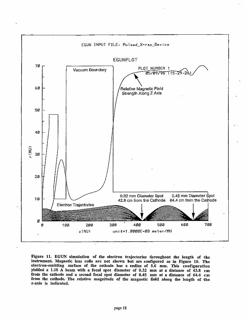
5.1 Simulation of Electron Trajectories
Figure 10 presents a detailed schematic of the instrument and the associated magnetic lens coils. Figure 11 displays the results of EGUN simulation using this configuration and includes both the electron trajectory paths and the relative magnetic field strength along the length of the z-axis.
page 16

10.0 cm
5.0 cm g S S S S w Z S H s p p p p i o p p i © p © © o © c alo.op.oTooc
3.8 cm
3 .oppe :ope ffoooooos
1.0 cm
3.0 cm
DEFLECTION PLATE
CHAMBER
8.0 cm
4.0 cm
2.0 cm
1.0 cm
20.0 cm
4.0 cm
20.0 cm - • - < 10.0 cm
4.0 cm
opldppyzpppl&pppppc ©js;oppXoj2.©;opAQPp.s 'oe!ooooooe*oe.».©.eo6:eeo:e: © O © © 8 S 0 0 0 0 0 5 0 0 Q Q O G O e c © ©'© O P © p ©p.© QppppplQpppifi © ©TO © © O p © Q.GQOQQ ©JX0&0JZ-C ©oT©o©©©©oTo©©©©o©T©o©©e «I*X*Isl*I*X^l2X*I^I*I»IeX«X8X*I*I«»
O&PPp'Opp.QOfi-»p>ppp*opp*ppp; s ® © ©©?©©©.©©£•
Mffl@@@@@@@ »p>-3©©:©©©:©©© s-p © © ©To © ©p o p a © © o © : © © © © © © s>p>ppp]pppopp s o p p o j p p p p p s SOS.O.OfeQOKO.C ©op ©p'© opppp © © O © ©Jp © ojppp o&ppplGppppp ©.©.© ©.oT&o.o.o.o.o » p o © p : © © p : © p G ooppploppppp © © © o ©To © ©:©.© © OJ5>ppp'<sppppp ®ppppi<&>ppppp o . o o s a i o s a o . o a
XS@©®©©©@® gnoppp'opp o p p pp>Ppp[0pp.Opp
© o.o.o © ©Te © ©Too e &pp>ppp:oppppp spppppioppppp a©©©©©;©©©.©©© ®K®®@R)©M0(@@IS
OGiGOppppppppapppieppppppmoppppppppppp © ©T© © © o p © ©Jp © p o p © ©!© © © © p p p M © p o p ©pip opppp ©o:©©©o©e©T©©©ooGoT©©©o©©CM©©o©©©:©o©T©©© ©©.©©•©©©©©.© ©.©_©.© © ©.© © G.O ©_© C M 3 O.O © ©.©.©©&.©.©.© ^ r a ^ & ^ ^ ^ r a u ^ ^ ^ ^ ^ ^ ^ ^ & ^ C y K & ^ ^ v f*CMP9E*X*X^*X*^**X"^ S G . O O Q O 6 O O . O O O O O O O K O 3 O O O C B S O 0 O O 6 S O O . S O C o ©:© © © opppp oppppp:Qppp>ppppp ©©Tp©©©©©©T©©©©©©©T©©©0©©GTp© ©©:©©©©©©©•©©©©©©©:©©©©©©©:©©
p » X ^ I ^ a E ^ I ^ J ^ ^ @ ^ ^ 4 t % ^ ^ X * S K % i 9 C ! ^ f f i © ©:© Qp©pppppppppp:opppppppp © ©T© © © © p p ©To op op ©p;© o s p p p p j p © © ©•©©©« o© ©•© © o ^ o © ©To ©©^©oo*©p © ©T© © © © p © ©T© © p o p © ©Top ®c>pp ©Tpp © ©!© © oppppp sppppplopppppplop ©©?©©©© ©©©?©©©©©©©!©©©©©©oT©©
f^@@@@@@@ra@g)@@@@@@@@ opppppppppppppppippppppppp QPIQGQQPPPIGQPPPPPIQPPPPPPIQC © ©I© © © ©.© o ©:© ©.© © © © ©;© o© <s> o © ©;o.c © ©'© © © ©P©©'© OPPP © QlOpppppppp
SAMPLE CHAMBER
31.0 cm
1.3 cm
12.8 cm
_ , M« APERTURE PLATE
21.6 cm
I I EXIT
WINDOW
ANODE
/ .
2.0 cm
Z/IX/S
Figure 10. Schematic (not to scale) displaying dimensions for the walls and magnet ic lens coils of the pulsed x-ray instrument. Save for the deflection plates and the anode, all important geometries are cylindrically symmetric. The electron-emitting section of the cathode has a radius of 5.6 mm, and the magnetic lens coils have a current density of 150 A«turns/cm 2.
page 17
EGUN INPUT FILE. Pulsed_X-ray_Device
0 100 200 300 400 500 600 700 z(MU) unit=1.0000E-03 meter/MU
Figure 11. EGUN simulation of the electron trajectories throughout the length of the instrument. Magnetic lens coils are not shown but are configured as in Figure 10. The electron-emitting surface of the cathode has a radius of 5.6 mm. This configuration yielded a 1.18 A beam with a focal spot diameter of 0.32 mm at a distance of 43.8 cm from the cathode and a second focal spot diameter of 0.45 mm at a distance of 64.4 cm from the cathode. The relative magnitude of the magnetic field along the length of the z-axis is indicated.
page 18

Of interest in Figure 10 is the uneven structure of the magnetic lens coils in the vicinity of the anode. Because space near the anode is to be occupied by the scintillator samples, the solenoid structure is disrupted. This naturally results in changes in the strength of the magnetic field in that area, leading to greater lens aberrations and a larger focal spot on the anode. In order to avoid this deleterious effect, the coils have been configured to maintain an approximately constant magnetic field strength in the vicinity of the anode. Figure 11 demonstrates that while the magnetic field near the end of the instrument does still experience small fluctuations, its average value remains approximately constant Hence good focusing is maintained.
The electron gun portion of the instrument shown in Figures 10 and 11 is actually a modified version of the Lawrence Berkeley National Laboratory Advanced Light Source (ALS) electron gun. While the ALS gun generates a current of 3.3 A, the current for this configuration is 1.18 A. Thus even if 10% of the electrons are lost to the grid and another 10% are lost to the aperture plate at the peak beam-aperture alignment, a peak anode current of 0.96 A will still be maintained.
The deflection plates are not depicted in Figure 10 because they do not demonstrate cylindrical symmetry. The plates are assumed to be approximately rectangular with a z-axis length of 10.0 cm, a width of 5.0 cm, and a separation distance of 3.5 cm. Lengthwise (i.e., in the direction of the z-axis) they are centered within the deflection plate chamber.
The EGUN simulation results of Figure 11 allow for a reasonable estimate of the resulting x-ray pulse time resolution. Assuming that a maximum deflection plate dV/dt of 1013 V/s is achieved, the post-aperture electron pulse width calculated with equation 8 is 8.6 ps. Equation 10 then yields an x-ray pulse width of 10.1 ps, very close to the desired time resolution.
5.2 Deflection Plate Sweeping Speed
The required deflection plate sweep speed of 1013 V/s can be achieved by properly implementing a power triode. The plates can then be modulated at an amplitude of 16 kV and a frequency of 100 MHz, yielding zero-crossing (i.e., maximum) dV/dt values that almost exactly match this goal. The specifications for an appropriate triode are given in Table 1.
Table 1. Technical specifications for CPI, Eimac Division 3CPX5000A7 High-Mu Power Triode. Data given are for pulse modulator or switch tube service. If necessary, more than one triode may be connected in parallel to increase current capabilities.
maximum voltage 16 kV peak current 67 A highest frequency for maximum ratings 110 MHz C 92.5 pF c '"nut
36.2 pF length 20.96 mm diameter 12.55 mm net weight 4.3 kg approximate cost $2600
The capacitance of the deflection plates is approximately 1.3 pF, with an additional estimated capacitance of 2 pF between the upper, modulated deflection plate and the instrument walls. Hence the peak current that results during the maximum dV/dt of 1013 V/s should only be about 33 A, well within the triode's specifications.
* This small deflection plate capacitance may present a problem, however, in that it is significantly smaller than the intrinsic capacitances of the power triode. As such, the power triode circuitry may have difficulty driving the deflection plates to the full 16 kV swing
page 19

unless the modulation circuit is carefully designed [13]. This would otherwise manifest as a decreased dV/dt and hence an increase in the x-ray pulse widths.
6.0 CONCLUSIONS
The conceptual design of a table-top device capable of producing 10 ps pulses of x-rays for ultra-fast fluorescence measurements has been presented. In addition to the very short timing resolution, the instrument provides 1 A peak anode current, 100 kHz repetition rate, and 120 keV peak x-ray energy. Each of these features is attractive for characterizing the fluorescent lifetimes and spectra of fast scintillators, providing for greater ease, and speed in measuring scintillation responses. The cost of the instrument is estimated at about $200,000 (U.S.).
The design challenge of achieving 10 ps x-ray pulses required consideration of numerous factors with complex interrelations. An advantageous geometry was chosen with the aid of EGUN simulations. Solenoidal magnetic lenses were selected as the primary means of containing and focusing the pulsed electron beam because of their ease of use and low level of aberration. It was determined that accelerating the electrons to 120 keV in the first stage rather than later provides for the best time resolution. Power triode modulation of the deflection plates was found to be the best means of achieving the very rapid voltage change of 10 V/s that is required to sweep the electron beam past the aperture in only 10 ps. Finally, in order to achieve the best impulse response it is indicated that both the anode angle and the delay element in the deflection plate-cathode grid synchronization circuitry should be adjustable so that they may be fine-tuned once the instrument is built.
Potential problems with the instrument include both the power triode circuitry failing to drive the plates to the full 16 kV modulation and excessive jitter in the deflection plate-cathode grid synchronization circuitry preventing the center (i.e., peak current region) of the electron pulses from aligning with the aperture during sweeping. Careful circuit design should limit these effects, however, and maintain the desired x-ray pulse characteristics.
REFERENCES
[1] S.E. Derenzo, W.W. Moses, R. Perera, et al, "Prospects for new inorganic scintillators," IEEE Transactions on Nuclear Science, 1990, vol. NS-37, pp. 203-208.
[2] S.E. Derenzo, W.W. Moses, J.L. Cahoon, et al., "X-ray fluorescence measurements of 412 inorganic compounds," in Conference Record of the 1991 Nuclear Science Symposium and Medical Imaging Conference, Santa Fe, New Mexico, Nov. 1991, vol. 1, pp. 143-147.
[3] S.E. Derenzo, W.W. Moses, S.C. Blankespoor, et al., "Design of a pulsed x-ray system for fluroescent lifetime measurements with a timing accuracy of 109 ps," IEEE Transactions on Nuclear Science, Jun. 1994, vol. 41, pp. 629-631.
[4] S.C. Blankespoor, "Design and characterization of a pulsed x-ray source for fluorescent lifetime measurements," Lawrence Berkeley National Laboratory Report, LBL-35092, UC-406, Dec. 1993, pp. 1-32.
[5] J.T.L. Thong, 'Ticosecond electron pulse generation via beam deflection-chopping in the SEM," Measurement Science and Technology, Mar. 1991, vol. 2, pp. 207-216.
[6] J.T.L. Thong, B.C. Breton, and W.C. Nixon, "High repetition rate electron beam chopping system for electron beam testing at microwave frequencies," Journal of Vacuum Science and Technology B, NovTDec. 1990, vol. 8, pp. 2048-2052.
page 20

[7] H. Sadorf and H.A. Kratz, "Plug-in fast electron beam chopping system," Review of Scientific Instruments, Apr. 1985, vol. 56, pp. 567-571.
[8] Personal communication, R.F Koontz, Stanford Linear Accelerator Center (SLAC), Dec. 1,1995, phone (415) 926-2528.
[9] W.B. Herrmannsfeldt, "EGUN: An Electron Optics and Gun Design Program," Stanford Linear Accelerator Center (SLAC)-Report-331, Oct. 1988, pp. 1-129.
[10] Personal communication, L. Veneklasen, E-Tech, Mar. 18, 1996, phone (510) 887-3307.
[11] A.B. El-Kareh and J.C.J. El-Kareh, Electron Optics, Lenses, and Beams, New York, Academic Press, 1970, pp. 250-256.
[12] R.F. Koontz, "Single-Bunch Beam Loading on the SLAC Two-Mile Accelerator," Stanford Linear Accelerator Center (SLAC) Report No. 195, May 1976, pp. 102-125.
[13] Personal communication, V.A. Mason, CPI, Eimac Division, Feb. 27, 1996, phone (415) 594-4061.
Reference to a company or product name does not imply approval or recommendation by the University of California or the U.S. Department of Energy to the exclusion of others that may be suitable.
page 21

o Recycled Paper