Comprehensive technology study of radiation hard LGADs
8
Comprehensive technology study of radiation hard LGADs E – L Gkougkousis a , L. Castillo Garcia b , S. Grinstein b , V. Coco a a EP-LBD, CERN, Route du Meyrin 285, CH-1211 Genève 23, Switzerland b IFAE, Edifici Cn, Campus UAB 08193 Bellaterra (Barcelona), Spain Corresponding Author: [email protected] Abstract: Towards radiation tolerant sensors for pico-second timing, several dopants are explored. Using a common mask, CNM produced LGADs with boron, boron + carbon and gallium implanted gain layers are studied under neutron and proton irradiation. With fluences ranging from 10 14 to 6 × 10 15 neq/cm 2 on both particle species, reported results focus on acceptor removal and gain reduction via electrical characterization. Timing performance, charge collection, gain and relative efficiency are treated through charged particle measurements, including signal analysis and noise characterization. An accent is placed on stability, via dark rate and operating voltage studies while, radiation related gain reduction mechanisms are examined comparing gain estimations through different approaches. 1. Introduction Towards HL-LHC upgrades, both ATLAS and CMS experiments envisage fast timing detectors for primary vertex separation and jet flavor tagging. Requirements vary from a per hit time resolution of 35 - 70 ps with a radiation hardness of 2.5×10 15 neq/cm 2 at 2.4 < |η| < 4.0 for the ATLAS High Granularity Timing Detector [1], to a 30 ps per track timing with a radiation tolerance of 1 × 10 15 neq/cm 2 at 1.6 < |η| < 3.0 for the CMS MIP Timing Detector [2]. Low Gain Avalanche Detectors (LGADs) [3] are considered as technology of choice for both experiments. In the LGAD process, the addition of a secondary p+ implant under the top n+ electrode, referend to as multiplication layer, results in an abrupt variation of the electric field close to the anode [4]. Such a geometry induces charge multiplication though impact ionization close to the multiplication layer region. 2. Radiation effects on LGADs Several radiation damage mechanisms degrading the performance of LGAD can be identified. At the substrate level, trapping leads to reduced carrier lifetime which compromises primary charge generation. The carrier lifetime τ is inversely proportional to radiation fluence (Φ) as described in (1). 1 ⁄ =× (1) Additionally, deep acceptor level introduction observed at high fluences, modifies the effective doping (Neff), leading to potential gain from the bulk, following (2). . =× (2) Fluence dependence of both these effects can be described by the β and G coefficients as defined by the ROSE collaboration [5].
Transcript of Comprehensive technology study of radiation hard LGADs

Comprehensive technology study of radiation hard LGADs
E – L Gkougkousisa, L. Castillo Garciab, S. Grinsteinb, V. Cocoa
a EP-LBD, CERN, Route du Meyrin 285, CH-1211 Genève 23, Switzerland b IFAE, Edifici Cn, Campus UAB 08193 Bellaterra (Barcelona), Spain
Corresponding Author: [email protected]
Abstract: Towards radiation tolerant sensors for pico-second timing, several dopants are
explored. Using a common mask, CNM produced LGADs with boron, boron + carbon and
gallium implanted gain layers are studied under neutron and proton irradiation. With fluences
ranging from 1014 to 6 × 10¹⁵ neq/cm2 on both particle species, reported results focus on
acceptor removal and gain reduction via electrical characterization. Timing performance,
charge collection, gain and relative efficiency are treated through charged particle
measurements, including signal analysis and noise characterization. An accent is placed on
stability, via dark rate and operating voltage studies while, radiation related gain reduction
mechanisms are examined comparing gain estimations through different approaches.
1. Introduction
Towards HL-LHC upgrades, both ATLAS and CMS experiments envisage fast timing detectors for
primary vertex separation and jet flavor tagging. Requirements vary from a per hit time resolution of
35 - 70 ps with a radiation hardness of 2.5×10¹⁵ neq/cm2 at 2.4 < |η| < 4.0 for the ATLAS High
Granularity Timing Detector [1], to a 30 ps per track timing with a radiation tolerance of 1 × 10¹⁵
neq/cm2 at 1.6 < |η| < 3.0 for the CMS MIP Timing Detector [2]. Low Gain Avalanche Detectors
(LGADs) [3] are considered as technology of choice for both experiments.
In the LGAD process, the addition of a secondary p+ implant under the top n+ electrode, referend
to as multiplication layer, results in an abrupt variation of the electric field close to the anode [4]. Such
a geometry induces charge multiplication though impact ionization close to the multiplication layer
region.
2. Radiation effects on LGADs
Several radiation damage mechanisms degrading the performance of LGAD can be identified. At the
substrate level, trapping leads to reduced carrier lifetime which compromises primary charge
generation. The carrier lifetime τ is inversely proportional to radiation fluence (Φ) as described in (1).
1 𝜏⁄ = 𝛽 × 𝛷 (1)
Additionally, deep acceptor level introduction observed at high fluences, modifies the effective doping
(Neff), leading to potential gain from the bulk, following (2).
𝑁𝐸𝑓𝑓. = 𝐺 × 𝛷 (2)
Fluence dependence of both these effects can be described by the β and G coefficients as defined by
the ROSE collaboration [5].

The multiplication layer is also affected by radiation. An active implant (NG0) reduction with fluence is
observed, described by the acceptor removal coefficient c as defined in (3) [6].
𝑁𝐺𝛷= 𝑁𝐺0
𝑒−𝑐𝛷 (3)
Finally, additional trapping and reduced mobility close to this region further limit impact ionization.
Through defect kinetics and interstitial diffusion, transformation of substitutional boron of the p+
multiplication layer to interstitial and subsequent formation of BiOi complexes (4) has been proven to
be detrimental due to trapping properties of the latter [7]. Introduction of carbon can disrupt this
mechanism by engaging oxygen in the formation of CiOi defects as detailed in (5). Replacement of
boron with gallium could also improve radiation hardness through expected reduced mobility of
gallium interstitials with respect to boron ones, as a result of their higher mass and reduced defect
formation cross-section.
𝑅𝑎𝑑𝑖𝑎𝑡𝑖𝑜𝑛 + 𝑆𝑖𝑠 → 𝑆𝑖 𝑖 + 𝐵𝑠 → 𝐵𝑖 + 𝑂 → 𝐵𝑖𝑂𝑖 (4)
𝑅𝑎𝑑𝑖𝑎𝑡𝑖𝑜𝑛 + 𝑆𝑖𝑠 → 𝑆𝑖 𝑖 + 𝐵𝑠 → 𝐶𝑖 + 𝑂 → 𝐶𝑖𝑂𝑖 (5)
In this study, a systematic evaluation of the radiation hardness of boron (B), boron + carbon (B+C)
and gallium (Ga) gain layer is presented, and the various radiation damage mechanisms are evaluated
though different methods. Samples were fabricated on 4” high resistivity (~2 kΩ×cm) Si-on-Si wafers
of 50 μm active thickness on 300 μm support wafer, following a “box-type” approximation, where the
p-multiplication layer is adjacent to the n layer with an abrupt transition (figure 1) [8]. Single diodes
are used with an active surface of 1 x 1 mm2, surrounded by a deep n+ junction terminator extension
(JTE) implant, a p-stop region and an n+ guard ring at the front side. A uniform p+ back-side implant
is implemented (figure 2). Six fluence points are studied, from 1 × 10¹⁴ to 6 × 10¹⁵ neq/cm2, using both
a 24 GeV/c proton beam and fast neutrons at CERN IRRAD and JSI facilities, respectively. No
thermal annealing was performed. All hereafter presented measurements were performed at three
distinct temperature points: -10oC, -20oC and -30oC.
Figure 1. Secondary Ion Mass Spectroscopy
(SiMS) extracted n+ anode and p+
multiplication layer doping profiles at the centre
of the active area.
Figure 2. Cross-section of a typical Si-on Si
wafer bonding LGAD diode geometry.
3. Active multiplication layer – The “Derive – Fit” method (DFM)
Evaluation of the radiation-induced active multiplication implant degradation can be performed by
studying the gain layer depletion voltage (VGL), under a linear dependence assumption. While C-V
studies for heavily irradiated sensors (> 1 × 10¹⁵ neq/cm2) remain challenging [9, 10], VGL can also be
obtained through I-V analysis. In a “box-type” approximation as above detailed, the Schottky-Mott
equation predicts a flexion point of the I-V characteristics at the gain layer depletion voltage. As a
result, the derivative of the I-V should pertain to a delta function convoluted to a gaussian, the width
of which is defined by the doping profile mixing function (e.g., deviation form a pure box-model) and

the measurement resolution. Consequently, VGL can be extracted by a gaussian fit of the I-V numerical
derivative (figure 3). It should be noted that such an approximation - referred to as the “Derive & Fit
Method” – DFM – should only be applied for continues profile transitions under a gaussian mixing
transition.
Figure 3. Numerical derivative of pad I-V
for different fluences with visible the
position of the gain layer depletion
voltage.
Figure 4. Numerical IV derivative and
corresponding gaussian fits at -10oC, -20oC and -
30oC for the same sample.
Applying DFM at different temperature points (-10oC, -20oC, -30oC, figure 4), a depletion voltage
is established for each sample. After normalization, the relative active multiplication implant is
estimated at each fluence point for all gain layer configurations (figure 5). Acceptor removal
coefficients (c) can subsequently be extracted (figure 6) by fitting (3) to each data series. No
significant variation of acceptor removal coefficient is observed between different multiplication layer
configurations. For all configurations, active implant degradation follows an identical trend with
respect to fluence for both neutron and non-NIEL normalized proton fluences. Ga samples present a
slight advantage under proton irradiation due to the more localized effect of the induced defects. The
implant’s higher mass can beneficially modify results in this approach since the fraction of implant-
activation related to direct interactions is marginally increased.
Figure 5. Relative active implant for all gain
layer configurations at different fluences. No
NIEL normalization applied. An exponential
fit is applied.
Figure 6. Acceptor removal coefficients for
neutron & proton irradiated samples with
NIEL normalization. No NIEL normalization
applied for combined calculation.
4. Effective Gain – GR vs Pad Method (GPM)
Through the DFM approach, gain layer de-activation via acceptor removal as described by (3) is
probed but, trapping effects and bulk acceptor level introduction are ignored. All three mechanisms
can be probed by effective gain estimation, obtained thought comparison of a non-multiplication vs

multiplication regions on the same die. Because of the unfirmly implanted die back side and p-stop
GR – pad isolation, two separate diodes can be considered at the same die. The first, formed between
the pad active area and backside, contains the multiplication layer while the second, defined between
the GR n-well and p-backside implant, is considered as a PIN diode. The leakage currents of the two
regions can be expressed by:
𝐼𝑝𝑎𝑑𝛷=0 = 𝑆 × 𝐼𝑠 × (𝑒
𝑒𝑉
𝑛𝑘𝑇 − 1) × 𝐺(𝑒𝑉, 𝑇, 0) and 𝐼𝐺𝑅𝛷=0 = 𝐼𝑠 × (𝑒
𝑒𝑉
𝑛𝑘𝑇 − 1) (6)
where S represents a geometry factor accounting for the difference in volume and shape of the
depleted regions, Is is the generation current and G(eV,T,Φ) the gain related contribution.
Following the alpha factor formalism [11], the radiation indued increase of the generation current
portion can be expressed as ΔIs = α × ΔΦ. By dividing the leakage currents of the two regions and
normalizing at Φ = 0, a gain-only dependent ratio is obtained (7):
|𝐼𝑝𝑎𝑑𝛷 𝐼𝐺𝑅
𝛷⁄ | = 𝑆 × 𝐺(𝑒𝑉, 𝑇, 𝛷) (7)
The Ipad/IGR ratio can be arithmetically calculated (figure 7). The exponential behavior with respect
to bias voltage becomes apparent following a Ipad/IGR = m × bV formalism. In such an approach, b
represents the gain induced increase of Ipad/IGR and can be extrapolated by a linear fit at the semi-
logarithmic plane.
Figure 7. Ipad/IGR versus bias voltage at the semi-log plane with the corresponding exponential fits for
different temperatures and fluences. A slope (b factor) reduction is observed with increased fluence.
The temperature dependence of gain imposes an equivalent dependence on b. Normalization with
respect to the unirradiated sample is therefore applied individually for each temperature of interest
(-10oC, -20oC & -30oC). The effective gain for all fluences and doping configurations is estimated
individually for proton and neutron irradiation (figures 8 & 9). This approach will be thereafter
referred to as the “Guard Ring vs Pad Method” – GPM.
Table 1. Effective gain removal coefficient for n0 and p+ irradiated samples on all gain layer
implementations
Gain layer
implementation
Effective gain removal coefficient
n0 irradiated p+ irradiated
Gallium (3.01 ± 0.9) × 10-14 (2.02 ± 0.11) × 10-14
Boron + Carbon (2.57 ± 1.1) × 10-15 (1.37 ± 0.24) × 10-14
Boron (2.25 ± 0.39) × 10-14 (2.25 ± 0.28) × 10-14
Using the modified effective doping formulation as defined by (8) [12] the removal coefficients c’
can be estimated (table 1) for all gain layer implementations. Identical acceptor re-introduction rates gc

and initial concentrations Neff,0 are assumed for all gain layer variations. As reported in table 1,
carbonated wafers present at least two times lower removal coefficients under proton irradiation with
respect to boron/gallium and up to 7 times under neutron. It is notable that estimated effective gain
removal coefficients are up to 10x higher than previously calculated acceptor removal coefficients.
𝑁𝑒𝑓𝑓(𝛷) = 𝑁𝑒𝑓𝑓0− 𝑁𝐶(1 − 𝑒−𝑐′𝛷) + 𝑔𝑐𝛷 (8)
Figure 8. Effective gain vs fluence for neutron
irradiated boron, carbon + boron and gallium
gain layer implementations.
Figure 9. Effective gain vs fluence for proton
irradiated samples. An increase at high
fluences is observed as a result of the deep
acceptor level re-introduction mechanism.
5. Real Gain estimation – Charged particle and timing measurements
Though both DMF and GMP, as previously presented, probe different parts of the radiation damage
mechanism, for a complete evaluation of all contributions, Minimum Ionizing Particles (MIPs)
measurements are required. To that end, β particles from a 90Sr source are used and collected charge,
time resolution, noise and rise time are evaluated at different bias voltages for all samples. Two-object
coincidence triggering is implemented (figure 10), using a known time resolution LGAD as a
reference. A 90 μm aluminum collimator blocks the 90Y lower energy contribution while a high
statistic of 5000 events per point is recorded. Collected charge is defined as the MPV of the Landau X
Gauss convoluted fit over the charge distribution of all collected events per bias point. A time-walk
correction via constant fraction discriminator is also utilized through CFD percentage optimization
maps (figure 11) and the point yielding the optimal time resolution is selected.
Figure 10. Exploded diagram of the charge
collection and timing measurement setup.
Figure 11. 2D - CFD optimization map with
time resolution at the colour axis.
An identical behaviour is observed prior to irradiation for all three gain layer implementations
across all temperatures (figure 12). For neutron irradiated samples, a 15% increase on the bias is
required for the gallium implanted samples to achieve an equivalent level of collected charge with
respect to boron. The trend persists across all fluences, irradiation species and temperatures of interest.

Regarding carbonated samples, an opposite behaviour is noted. Same charge levels are obtained at a
20% lower biasing with respect to boron only samples, across all fluences, irradiation types and
temperatures.
Figure 12. Charge collection at three different temperatures for both neutron and proton irradiated
samples of all gain layer configurations. Minimum ASIC requirements are set along the 5 fC line.
For all doping types, proton irradiated samples require a factor of two increase in bias votlage to
reach equivalent perfromance with respect to neutron irradiation. The previously described picture, in
regards of doping type, temperature and irradiation type is reflected unchanged on time resolution
results. It must be noted that all samples achieve the 30 -70 ps requirements imposed by both ATLAS
and CMS experiments (figure 13). Further signal analysis does not reveal any pulse-shape variations
realted to doping type as can be seen for example in the rise time (figue 14). All implementations have
similar signal characteristics and are suitable for timing.
Figure 13. Timing resolution of all gain
configuration at difference fluences. An under
70 ps resolution is achieved at all cases.
Figure 14. Rise time for different gain layer
configurations and irradiation level. As gain is
reduced, signals become faster asymptotically
approaching primary charges collection time.
6. Comparative Studies
6.1. Leakage current evaluation
Evaluation of possible effects in leakage current across different gain layer doping types is caried out
though I-V analysis. A comparison of non-gain regions between carbonated and standard boron
samples reveals a 38% increase of leakage current for the earlier. Such an increase is unrelated to the
enhanced gain observed for carbonated devices after irradiation and is consistently measured for
fluences of up to 1 × 10¹⁵ neq/cm2 on both protons and neutrons across all temperatures (figure 15). At
higher fluences, increase due to radiation induced damage current prevails, rendering prohibitive any
meaningful comparison.

Figure 15. Ratio between leakage current of the carbonated and non-carbonated samples at a region
after depletion and below breakdown for different fluences, irradiation species and temperatures.
6.2. Operational Stability
Stability of all devices was evaluated though an extensive dark rate study. With no external stimulus,
four continuous self-trigger events within a time frame of up to 5 min were recorded, and a median
rate was extracted. In such a way cosmic rejection is guaranteed. The process is repeated 1000 times
for each voltage point and a rate distribution is obtained (figure 16). After a poissonian fit,
extrapolated median rate is considered as the dark rate value corresponding to the specified bias.
Through bias voltage scanning, s-like stability curves are obtained for each sample (figure 17).
Figure 16. Distribution of normalized dark rate
event frequency for boron-only gain layer at
490 V, irradiated at 3 × 10¹⁵ neq/cm2.
Figure 17. S-stability curves for all samples at
-30oC. Each point is equal to the median of the
corresponding poissonian fit.
An exponential increase in dark rate is observed at bias voltages up to 10-15 V lower than the
established breakdown point of the device. For carbonated samples, a 20% decrease of the stable
operating voltage point is noted with respect to boron-only multiplication layer. On the contrary, for
gallium implanted samples, the situation is inversed with a 10% increase at the operation point. Such
behavior is expected and in agreement with the charge collected measurements.
6.3. Efficiency and Headroom
An efficiency estimation is performed by evaluation of the recorded event frequency under the
stability assumption of the employed source. The headroom can then be defined as the distance
between the operating bias and the point at which the determined dark rate becomes equal to 10% of
the real event rate. Under these conditions, an efficiency vs headroom study is possible, using the
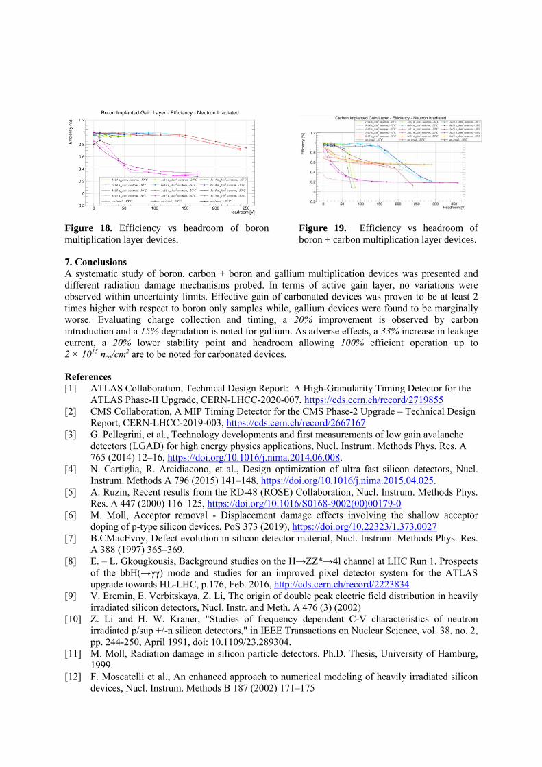
entirety of recorded statistics for each bias point (figure 18 and 19).
A 100% efficiency under stable operation is reachable for fluences up to 3 × 10¹⁵neq/cm2 for
standard boron gain layer samples but is not the case for carbonated devices. The higher expected gain
in insufficient to compensate for instabilities at fluences greater than ~ 2 × 10¹⁵neq/cm2.
7. Conclusions
A systematic study of boron, carbon + boron and gallium multiplication devices was presented and
different radiation damage mechanisms probed. In terms of active gain layer, no variations were
observed within uncertainty limits. Effective gain of carbonated devices was proven to be at least 2
times higher with respect to boron only samples while, gallium devices were found to be marginally
worse. Evaluating charge collection and timing, a 20% improvement is observed by carbon
introduction and a 15% degradation is noted for gallium. As adverse effects, a 33% increase in leakage
current, a 20% lower stability point and headroom allowing 100% efficient operation up to
2 × 10¹⁵ neq/cm2 are to be noted for carbonated devices.
References
[1] ATLAS Collaboration, Technical Design Report: A High-Granularity Timing Detector for the
ATLAS Phase-II Upgrade, CERN-LHCC-2020-007, https://cds.cern.ch/record/2719855
[2] CMS Collaboration, A MIP Timing Detector for the CMS Phase-2 Upgrade – Technical Design
Report, CERN-LHCC-2019-003, https://cds.cern.ch/record/2667167
[3] G. Pellegrini, et al., Technology developments and first measurements of low gain avalanche
detectors (LGAD) for high energy physics applications, Nucl. Instrum. Methods Phys. Res. A
765 (2014) 12–16, https://doi.org/10.1016/j.nima.2014.06.008.
[4] N. Cartiglia, R. Arcidiacono, et al., Design optimization of ultra-fast silicon detectors, Nucl.
Instrum. Methods A 796 (2015) 141–148, https://doi.org/10.1016/j.nima.2015.04.025.
[5] A. Ruzin, Recent results from the RD-48 (ROSE) Collaboration, Nucl. Instrum. Methods Phys.
Res. A 447 (2000) 116–125, https://doi.org/10.1016/S0168-9002(00)00179-0
[6] M. Moll, Acceptor removal - Displacement damage effects involving the shallow acceptor
doping of p-type silicon devices, PoS 373 (2019), https://doi.org/10.22323/1.373.0027
[7] B.CMacEvoy, Defect evolution in silicon detector material, Nucl. Instrum. Methods Phys. Res.
A 388 (1997) 365–369.
[8] E. – L. Gkougkousis, Background studies on the H→ZZ*→4l channel at LHC Run 1. Prospects
of the bbH(→γγ) mode and studies for an improved pixel detector system for the ATLAS
upgrade towards HL-LHC, p.176, Feb. 2016, http://cds.cern.ch/record/2223834
[9] V. Eremin, E. Verbitskaya, Z. Li, The origin of double peak electric field distribution in heavily
irradiated silicon detectors, Nucl. Instr. and Meth. A 476 (3) (2002)
[10] Z. Li and H. W. Kraner, "Studies of frequency dependent C-V characteristics of neutron
irradiated p/sup +/-n silicon detectors," in IEEE Transactions on Nuclear Science, vol. 38, no. 2,
pp. 244-250, April 1991, doi: 10.1109/23.289304.
[11] M. Moll, Radiation damage in silicon particle detectors. Ph.D. Thesis, University of Hamburg,
1999.
[12] F. Moscatelli et al., An enhanced approach to numerical modeling of heavily irradiated silicon
devices, Nucl. Instrum. Methods B 187 (2002) 171–175
Figure 18. Efficiency vs headroom of boron
multiplication layer devices.
Figure 19. Efficiency vs headroom of
boron + carbon multiplication layer devices.