Comprehensive study of the metal-insulator transition in...
7
Comprehensive study of the metal-insulator transition in pulsed laser deposited epitaxial VO 2 thin films Deyi Fu, 1,2,a) Kai Liu, 1,3,a) Tao Tao, 2 Kelvin Lo, 1 Chun Cheng, 1 Bin Liu, 2 Rong Zhang, 2 Hans A. Bechtel, 4 and Junqiao Wu 1,3,b) 1 Department of Materials Science and Engineering, University of California, Berkeley, California 94720, USA 2 Jiangsu Provincial Key Laboratory of Advanced Photonic and Electronic Materials, School of Electronic Science and Engineering, Nanjing University, Nanjing, Jiangsu 210093, China 3 Materials Sciences Division, Lawrence Berkeley National Laboratory, Berkeley, California 94720, USA 4 Advanced Light Source, Lawrence Berkeley National Laboratory, Berkeley, California 94720, USA (Received 25 October 2012; accepted 4 January 2013; published online 24 January 2013) In this paper, we present a comprehensive, correlative study of the structural, transport, optical and thermoelectric properties of high-quality VO 2 thin films across its metal-insulator phase transition. Detailed x-ray diffraction study shows that it’s textured polycrystalline along [010] M1 , with in-plane lattice orienting along three equivalent crystallographic directions. Across the metal-insulator transition, the conductivity increases by more than 3 orders of magnitude with a value of 3.8 10 3 S/cm in the metallic phase. This increase is almost entirely accounted for by a change in electron density, while the electron mobility changes only slightly between the two phases, yet shows strong domain boundary scattering when the two phases coexist. Electron effective mass was determined to be 65m 0 in the insulating phase. From the optical and infrared reflection spectra in the metallic phase, we obtained the plasma edge of VO 2 , from which the electron effective mass was determined to be 23m 0 . The bandgap of VO 2 was determined from optical absorption to be 0.70 6 0.05 eV at room temperature and rapidly shrinks before the phase transition occurs. In the temperature range where metallic and insulating phases coexist, the Seebeck coefficient was found to be significantly lower than that predicted by a linear combination of volumetric contributions from the insulating and metallic domains, indicating abnormal thermoelectric effect at the metal/insulator domain walls in such two-dimensional domain structure. V C 2013 American Institute of Physics.[http://dx.doi.org/10.1063/1.4788804] I. INTRODUCTION Vanadium oxides exhibiting metal-insulator transition (MIT) at various temperatures are of great interest in materials science for both fundamental understanding of correlated elec- tron physics and potential device applications. Among them, vanadium dioxide (VO 2 ) has been studied most intensively owing mostly to its near-room-temperature phase transition as well as its high phase stability. 1 It undergoes a first-order MIT around 68 C from a high-temperature metallic (M) phase to a low-temperature insulating (I) phase, which is accompanied by a structural phase transition from a high-temperature tet- ragonal (Rutile, R) structure to a low-temperature monoclinic (M1) structure. 2–6 Both theoretical and experimental efforts have been devoted to understanding and exploiting the mecha- nism of MIT since the early work of Morin decades ago. 7 However, due to the complex phase diagram of VO 2d with different stoichiometries, as well as complications arising from coexisting metal/insulator domains across the MIT, the synthesis and characterization of VO 2 have never been easy. Thanks to rapid advances in growth of thin-film oxides in recent years such as molecular beam epitaxy, 8 chemical vapor deposition, 9 sol-gel deriving, 10 sputtering, 11 and pulsed laser deposition, 12 the study of VO 2 is reviving, with growing emphasis on exploring its device applications. Applications such as thermo/electrochromics, 13 Mott transistors, 14 strain sensors, 15 and thermal actuators 16 have been proposed or real- ized based on the MIT of VO 2 . However, a systematic, comprehensive study of the phys- ical properties of these high-quality VO 2 specimens across the MIT has been lacking; for example, electrical transport prop- erties were measured without optical and infrared characteri- zation of the same sample 17 and vice versa. 18 As a result, correlations across different aspects of the MIT are yet to be identified and cross-checked, which could reveal some intrin- sic materials properties out of merely sample-specific effects, or answer outstanding questions on VO 2 . In this work, we present a comprehensive study of high-quality VO 2 thin films grown by pulsed laser deposition, fully characterizing their structural, electrical transport, optical (including infrared), and thermoelectric properties altogether. These include: (1) The growth direction of epitaxial VO 2 thin films on sapphire is identified to be [010] M1 instead of [001] M1 , a controversy from previous reports. Identification of the film texturing direction is important to simulation of energetics of the VO 2 phase transition strain, 19 as well as the very recent effort of using VO 2 as an active material for MEMS actuation; 20 (2) An unusually strong electron scattering by M-I domain boun- daries is revealed from the electron mobility drop during the inhomogeneous MIT of VO 2 . Such effect disappear when the a) Deyi Fu and Kai Liu contributed equally to this work. b) Author to whom correspondence should be addressed. Electronic mail: [email protected]. 0021-8979/2013/113(4)/043707/7/$30.00 V C 2013 American Institute of Physics 113, 043707-1 JOURNAL OF APPLIED PHYSICS 113, 043707 (2013)
Transcript of Comprehensive study of the metal-insulator transition in...

Comprehensive study of the metal-insulator transition in pulsed laserdeposited epitaxial VO2 thin films
Deyi Fu,1,2,a) Kai Liu,1,3,a) Tao Tao,2 Kelvin Lo,1 Chun Cheng,1 Bin Liu,2 Rong Zhang,2
Hans A. Bechtel,4 and Junqiao Wu1,3,b)
1Department of Materials Science and Engineering, University of California, Berkeley, California 94720, USA2Jiangsu Provincial Key Laboratory of Advanced Photonic and Electronic Materials, School of ElectronicScience and Engineering, Nanjing University, Nanjing, Jiangsu 210093, China3Materials Sciences Division, Lawrence Berkeley National Laboratory, Berkeley, California 94720, USA4Advanced Light Source, Lawrence Berkeley National Laboratory, Berkeley, California 94720, USA
(Received 25 October 2012; accepted 4 January 2013; published online 24 January 2013)
In this paper, we present a comprehensive, correlative study of the structural, transport, optical and
thermoelectric properties of high-quality VO2 thin films across its metal-insulator phase transition.
Detailed x-ray diffraction study shows that it’s textured polycrystalline along [010]M1, with
in-plane lattice orienting along three equivalent crystallographic directions. Across the
metal-insulator transition, the conductivity increases by more than 3 orders of magnitude with a
value of 3.8� 103 S/cm in the metallic phase. This increase is almost entirely accounted for by a
change in electron density, while the electron mobility changes only slightly between the two
phases, yet shows strong domain boundary scattering when the two phases coexist. Electron
effective mass was determined to be �65m0 in the insulating phase. From the optical and infrared
reflection spectra in the metallic phase, we obtained the plasma edge of VO2, from which the
electron effective mass was determined to be �23m0. The bandgap of VO2 was determined from
optical absorption to be 0.70 6 0.05 eV at room temperature and rapidly shrinks before the phase
transition occurs. In the temperature range where metallic and insulating phases coexist, the
Seebeck coefficient was found to be significantly lower than that predicted by a linear combination
of volumetric contributions from the insulating and metallic domains, indicating abnormal
thermoelectric effect at the metal/insulator domain walls in such two-dimensional domain
structure. VC 2013 American Institute of Physics. [http://dx.doi.org/10.1063/1.4788804]
I. INTRODUCTION
Vanadium oxides exhibiting metal-insulator transition
(MIT) at various temperatures are of great interest in materials
science for both fundamental understanding of correlated elec-
tron physics and potential device applications. Among them,
vanadium dioxide (VO2) has been studied most intensively
owing mostly to its near-room-temperature phase transition as
well as its high phase stability.1 It undergoes a first-order MIT
around 68 �C from a high-temperature metallic (M) phase to a
low-temperature insulating (I) phase, which is accompanied
by a structural phase transition from a high-temperature tet-
ragonal (Rutile, R) structure to a low-temperature monoclinic
(M1) structure.2–6 Both theoretical and experimental efforts
have been devoted to understanding and exploiting the mecha-
nism of MIT since the early work of Morin decades ago.7
However, due to the complex phase diagram of VO2�d with
different stoichiometries, as well as complications arising
from coexisting metal/insulator domains across the MIT, the
synthesis and characterization of VO2 have never been easy.
Thanks to rapid advances in growth of thin-film oxides in
recent years such as molecular beam epitaxy,8 chemical vapor
deposition,9 sol-gel deriving,10 sputtering,11 and pulsed laser
deposition,12 the study of VO2 is reviving, with growing
emphasis on exploring its device applications. Applications
such as thermo/electrochromics,13 Mott transistors,14 strain
sensors,15 and thermal actuators16 have been proposed or real-
ized based on the MIT of VO2.
However, a systematic, comprehensive study of the phys-
ical properties of these high-quality VO2 specimens across the
MIT has been lacking; for example, electrical transport prop-
erties were measured without optical and infrared characteri-
zation of the same sample17 and vice versa.18 As a result,
correlations across different aspects of the MIT are yet to be
identified and cross-checked, which could reveal some intrin-
sic materials properties out of merely sample-specific effects,
or answer outstanding questions on VO2. In this work, we
present a comprehensive study of high-quality VO2 thin films
grown by pulsed laser deposition, fully characterizing their
structural, electrical transport, optical (including infrared), and
thermoelectric properties altogether. These include: (1) The
growth direction of epitaxial VO2 thin films on sapphire is
identified to be [010]M1 instead of [001]M1, a controversy
from previous reports. Identification of the film texturing
direction is important to simulation of energetics of the VO2
phase transition strain,19 as well as the very recent effort of
using VO2 as an active material for MEMS actuation;20 (2)
An unusually strong electron scattering by M-I domain boun-
daries is revealed from the electron mobility drop during the
inhomogeneous MIT of VO2. Such effect disappear when the
a)Deyi Fu and Kai Liu contributed equally to this work.b)Author to whom correspondence should be addressed. Electronic mail:
0021-8979/2013/113(4)/043707/7/$30.00 VC 2013 American Institute of Physics113, 043707-1
JOURNAL OF APPLIED PHYSICS 113, 043707 (2013)

film is in pure M or I phase, therefore must originate from
scattering of electrons at the interface between M and I
phases, and differ from the ordinary grain boundary scattering.
It may need to be included for properly analyzing free charge
dynamics in optical studies of VO2 films in the M-I phase co-
existing regime;18 (3) From the plasma edge on the infrared
reflectance, we determine the electron effective mass in the
M-phase, which is cross-checked by independent Seebeck
measurement; (4) By combining Hall and Seebeck measure-
ments, we conclude that lattice (acoustic phonon) scattering of
conductive electrons in the M-phase is negligible; (5) The
Fermi level in the I-phase is determined by temperature-
dependent Seebeck measurement, which is then combined
with the temperature-dependent Hall data to evaluate the elec-
tron effective mass of the I-phase; (6) Combining Hall mobil-
ity data and Seebeck results highlights the important unusual
thermoelectric contribution of M-I domain walls during the in-
homogeneous MIT of the thin film system, which proves that
this domain wall effect is not limited to 1D VO2 nanobeams;21
(7) The bandgap of I-phase VO2 is determined, and its temper-
ature dependence is found to be an order of magnitude stron-
ger than that of non-correlated, traditional semiconductors.
These results are expected to help further understanding of
this correlated electron oxide, as well as its future device
applications in electronics and electro-optics.
II. EXPERIMENTAL
The VO2 thin films used in this study were grown on
c-plane sapphire (i.e., (0001)-Al2O3) substrate by pulsed
laser deposition. A KrF excimer laser (k¼ 248 nm) was
focused onto a target (pressed 99.9% pure VO2 powder, den-
sity �4.0 g/cm3) with a fluence of �1.3 J/cm2. The deposi-
tion chamber was pumped to �10�6 Torr before oxygen gas
was introduced into the chamber. The deposition was per-
formed in oxygen ambient of 10 mTorr with substrate tem-
perature maintained at 530 �C for 2.5 h. After the deposition,
the samples were cooled down at a rate of 10 �C/min to room
temperature at the deposition oxygen pressure. The thickness
of the as-grown film was determined to be �250 nm by
cross-sectional scanning electron microscopy and atomic
force microscopy (AFM).
The crystallinity of the films at room temperature (M1-
structure) was first identified by high resolution x-ray diffrac-
tion, which was performed using a triple-axis diffractometer
equipped with a four-crystal Ge (220) monochromator and a
three reflection Ge (220) analyzer in a PANalytical X’Pert
Pro MRD system. The Cu Ka line (k¼ 0.154 nm) radiated
from a 2.2 kW ceramic tube with resolution limit of about 12
arc sec was used as the x-ray source.
Transport properties across the MIT, such as temperature
dependence of the electrical resistivity/conductivity, carrier
density and Hall mobility, were measured based on van der
Pauw geometry using an Ecopia HMS-3000 Hall measure-
ment system. The sample temperature was controlled by a
Lake Shore 325 temperature controller with high temperature
stability and was calibrated with a thin type-K thermocouple.
To investigate optical properties across the MIT, both
reflection and transmission spectra were taken from ultraviolet
to the infrared wavelength range. The mid-infrared spectra
between 1600 cm�1 and 7000 cm�1 were measured using a
Fourier-transform infrared spectrometer (Thermo Nicolet
Nexus870) combined with a confocal microscope (Nicolet
ContinuumXL) using a 32� Schwarzschild objective (numeri-
cal aperture:0.65), and the signal was collected with a liquid-
nitrogen-cooled mercury cadmium telluride (MCT-A)
detector (as shown elsewhere22). The ultraviolet-visible-near-
infrared spectra between 320 nm and 2600 nm were measured
using a PerkinElmer LAMBDA 750 UV/Vis/NIR spectropho-
tometer, where the signal below 890 nm was collected by a
photomultiplier tube and that above 890 nm was collected by
a PbS detector.
A rectangular sample (�10 mm� 5 mm) with Ohmic
contacts (15 nm Cr/200 nm Au) on the two ends of the stripe
was prepared for the Seebeck measurement. The Seebeck
measurement was carried out by suspending the sample
between two temperature controlled copper blocks, which
were enclosed inside a small vacuum chamber providing
pressures as low as 9� 10�7 Torr. High temperatures were
produced by passing current through resistive heaters in each
sample block. The temperature at each end of the sample
was monitored by affixing type-T thermocouples to either
end using small pieces of indium foil to ensure good thermal
contact to the sample.
III. RESULTS AND DISCUSSION
A. Structural properties
Figure 1(a) shows the XRD 2h/x scan spectra of the as-
grown VO2 thin film at room temperature. The well-resolved
sharp peaks at 41.94� and 90.98� correspond to diffraction
peaks from the c-plane of the substrate, namely sap-
phire(0006) and sapphire(00012), respectively. However, the
origin of the peak located around 40.02� and its secondary
peak at 85.97� have been controversial, and they have been
indexed as either (020)M1/(040)M1 peaks, or (002)M1/(004)M1
peaks, of VO2 by different groups.12,23–26 The discrepancy
originates from the fact that (010)M1 and (001)M1 planes of
VO2 have almost the same lattice spacing, therefore nearly
the same Bragg diffraction angle, which makes them undis-
tinguishable by using only 2h/x scan. In order to solve the
problem and also explore the in-plane texturing of the film,
off-axis u scan of VO2 (110)M1 planes were performed
because they have significantly different inclination angles
to the VO2 (010)M1 and (001)M1 planes. As shown in
Fig. 1(b), only the diffraction peaks from the u scan patterns
corresponding to the [010]M1 growth direction (W¼ 43.1�,2h¼ 26.86�) were found, which verifies high-quality crystal-
line VO2 with its (010)M1 plane (rather than (001)M1 plane)
parallel to the substrate. The high quality of the film is evi-
dent from the relative small full width at half-maximum
(FWHM �0.15�) of the rocking curve of the (020)M1 diffrac-
tion peak as shown in the inset of Fig. 1(a). We note that the
VO2 peaks and their rocking curves slightly deviate from an
ideal Gaussian shape, which is indicative of high residual
strain in the thin film due to lattice and thermal mismatches
between the VO2 and the substrate. Furthermore, clear six-
fold symmetry of the off-axis u scan spectra from the
043707-2 Fu et al. J. Appl. Phys. 113, 043707 (2013)
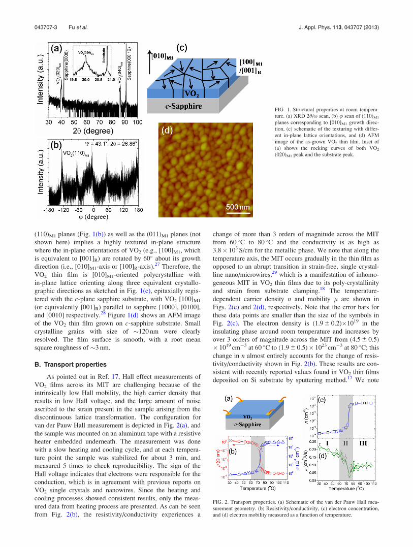
(110)M1 planes (Fig. 1(b)) as well as the (011)M1 planes (not
shown here) implies a highly textured in-plane structure
where the in-plane orientations of VO2 (e.g., [100]M1, which
is equivalent to [001]R) are rotated by 60� about its growth
direction (i.e., [010]M1-axis or [100]R-axis).27 Therefore, the
VO2 thin film is [010]M1-oriented polycrystalline with
in-plane lattice orienting along three equivalent crystallo-
graphic directions as sketched in Fig. 1(c), epitaxially regis-
tered with the c-plane sapphire substrate, with VO2 [100]M1
(or equivalently [001]R) parallel to sapphire [1000], [0100],
and [0010] respectively.28 Figure 1(d) shows an AFM image
of the VO2 thin film grown on c-sapphire substrate. Small
crystalline grains with size of �120 nm were clearly
resolved. The film surface is smooth, with a root mean
square roughness of �3 nm.
B. Transport properties
As pointed out in Ref. 17, Hall effect measurements of
VO2 films across its MIT are challenging because of the
intrinsically low Hall mobility, the high carrier density that
results in low Hall voltage, and the large amount of noise
ascribed to the strain present in the sample arising from the
discontinuous lattice transformation. The configuration for
van der Pauw Hall measurement is depicted in Fig. 2(a), and
the sample was mounted on an aluminum tape with a resistive
heater embedded underneath. The measurement was done
with a slow heating and cooling cycle, and at each tempera-
ture point the sample was stabilized for about 3 min, and
measured 5 times to check reproducibility. The sign of the
Hall voltage indicates that electrons were responsible for the
conduction, which is in agreement with previous reports on
VO2 single crystals and nanowires. Since the heating and
cooling processes showed consistent results, only the meas-
ured data from heating process are presented. As can be seen
from Fig. 2(b), the resistivity/conductivity experiences a
change of more than 3 orders of magnitude across the MIT
from 60 �C to 80 �C and the conductivity is as high as
3.8� 103 S/cm for the metallic phase. We note that along the
temperature axis, the MIT occurs gradually in the thin film as
opposed to an abrupt transition in strain-free, single crystal-
line nano/microwires,29 which is a manifestation of inhomo-
geneous MIT in VO2 thin films due to its poly-crystallinity
and strain from substrate clamping.18 The temperature-
dependent carrier density n and mobility l are shown in
Figs. 2(c) and 2(d), respectively. Note that the error bars for
these data points are smaller than the size of the symbols in
Fig. 2(c). The electron density is (1.9 6 0.2)�1019 in the
insulating phase around room temperature and increases by
over 3 orders of magnitude across the MIT from (4.5 6 0.5)
� 1019 cm�3 at 60 �C to (1.9 6 0.5)� 1023 cm�3 at 80 �C; this
change in n almost entirely accounts for the change of resis-
tivity/conductivity shown in Fig. 2(b). These results are con-
sistent with recently reported values found in VO2 thin films
deposited on Si substrate by sputtering method.17 We note
FIG. 1. Structural properties at room tempera-
ture. (a) XRD 2h/x scan, (b) u scan of (110)M1
planes corresponding to [010]M1 growth direc-
tion, (c) schematic of the texturing with differ-
ent in-plane lattice orientations, and (d) AFM
image of the as-grown VO2 thin film. Inset of
(a) shows the rocking curves of both VO2
(020)M1 peak and the substrate peak.
FIG. 2. Transport properties. (a) Schematic of the van der Pauw Hall mea-
surement geometry. (b) Resistivity/conductivity, (c) electron concentration,
and (d) electron mobility measured as a function of temperature.
043707-3 Fu et al. J. Appl. Phys. 113, 043707 (2013)

that the measured electron density in the metallic phase corre-
sponds to approximately 7 6 2 electrons contributed by each
vanadium atom since the number density of vanadium atoms
in VO2 is about 3� 1022 cm�3.2 The observation of more
than one conduction electron per vanadium atom has been
reported before by different groups2,17,30 and was explained
as two types of carriers co-existing in the system. While the
electron density n changes monotonically with temperature,
the evolution of mobility l shows some complexity as seen
in Fig. 2(d). The overall mobility in the insulating phase is
higher than that in the metallic phase. The whole process can
be divided into three regimes: when T<� 60 �C (regime-I),
the mobility slightly decreases with increasing temperature;
when the temperature further increases and the inhomogene-
ous MIT and structural transition start to occur (60 �C<T
< 80 �C, regime-II), the mobility decreases drastically by a
factor of 4, which can be mainly attributed to strong scatter-
ing of electrons at the boundaries of metallic and insulating
(semiconducting) domains; when the system finally becomes
fully metallic (T>� 80 �C, regime-III), the electron mobility
partially recovers because the phase boundary scattering
effect disappears (even though the structural grain boundaries
still exist). We note that the mobility in the metallic phase
stays almost a constant upon further heating, suggesting that
the mobility there is not governed by acoustic phonon scatter-
ing, because phonon scattering would become stronger when
temperature rises.
C. Optical and infrared properties
Figure 3 shows the measured optical reflection spectra of
the VO2 thin film at selected temperatures during heating. The
dashed line distinguishes the spectra measured from two dif-
ferent systems as described in the experimental section. The
periodic fringes seen in the insulating-phase spectra (�65 �C)
result from interference between light reflected from the sam-
ple top and bottom surfaces (Fabry-Perot oscillation). This in-
terference disappears for the metallic phase due to strong
optical absorption by the film. Across the MIT, the reflectivity
underwent a drastic change, especially in the infrared region
(<10 000 cm�1). In the metallic phase (>82 �C), the optical
response of the film is dominated by its free carriers and shows
high infrared reflectivity. The surface reflection of conductors
by free carriers is frequently used to determine the effective
mass of free carriers, which can be calculated from the plasma
frequency (xP), provided that the carrier concentration(n) and
the optical dielectric constant (e1) are known,31 i.e.
m� ¼ ne2
e0e1x2P
; (1)
where e0 is the vacuum permittivity and e is elementary elec-
tron charge. Here, we note that the plasma reflection edge in
the insulating-phase is not resolved due to relatively low
electron concentration (thus low plasma frequency) and the
Fabry-Perot feature. The infrared reflection spectrum for the
metallic phase can be fitted using a standard complex dielec-
tric function model that includes finite lifetime broadening,31
from which xP and the damping parameter were determined
to be 10 500 cm�1 and 15 000 cm�1, respectively, as shown
in the inset of Fig. 3. Using the optical dielectric constant
e1¼ 9 as suggested by Barker et al.,32 we estimated the
electron effective mass in the metallic phase to be �23m0.
This is heavier than previously reported results, which show
a range of values between 3.5m030 and 7.1m0.33 The higher
m* is mainly due to higher free electron density measured in
our films and used in the calculation. This high electron den-
sity may also arise from the high residual strain existing in
the films.
Optical absorption (a) spectra of the VO2 thin film
were obtained by considering the reflection loss, It
¼ I0ð1� RÞe�ad , where d is the film thickness, R¼ Ir=I0 is
the reflection, and It=I0 is defined as transmission T. The
value of a converted from measured R and T are shown in
Fig. 4(a). A clear onset of absorption at around 0.7 eV can be
seen in the insulating phase, which is associated with optical
transition across the fundamental bandgap of VO2. Above
the threshold energy, the absorption increases rapidly and
gradually saturates at around 1.5 eV� 2.0 eV, after which
the absorption rapidly increases again. The rapid increase
beyond �2.0 eV can be attributed to transition to the con-
duction band (derived from vanadium 3d-orbitals) from the
FIG. 3. Reflection spectra of VO2 thin film across a wide spectral range at
different temperatures (in units �C). Note that the spectra on the two sides of
the vertically dashed line were measured using two different spectroscopy
systems. The inset shows the measured and fitted results of the reflection
spectrum of VO2 in the high-temperature metallic phase.
FIG. 4. (a) Absorption coefficient of VO2 thin film over a wide spectral
range at different temperatures (in units �C). Note that the spectra on the
two sides of the vertically dashed line were measured using two different
spectroscopy systems. (b) Square of the absorption coefficient of VO2 used
to determine the absorption edge of the material. The inset shows the rapid
shrink of the absorption edge as a function of temperature.
043707-4 Fu et al. J. Appl. Phys. 113, 043707 (2013)

low-lying oxygen 2p band, which was reported to be �2 eV
below the 3d orbitals.2 According to the Tauc relation, the
absorption coefficient for direct-bandgap material near the
band edge can be modeled as34
aðh�Þ ¼ Affiffiffiffiffiffiffiffiffiffiffiffiffiffiffiffih� � Eg
p; (2)
where Eg is the energy gap and A is a constant depending on
the material. In Fig. 4(b), we plotted a2 as a function of pho-
ton energy. By fitting the linear section of the absorption
spectra and extrapolating to the axis, we determined the
bandgap of insulating-phase VO2. When the temperature
increases toward the MIT temperature, the effective bandgap
gradually decreases, from 0.70 6 0.05 eV at 30 �C to 0.58
6 0.05 eV at 66.3 �C. This bandgap narrowing of 0.12 eV
from 30 to 66.3 �C (inset of Fig. 4(b)) is an order of magni-
tude faster than traditional semiconductors. For example, for
InN and GaSb, two direct-bandgap semiconductors with
comparable bandgap value to VO2, the bandgap narrows by
0.010 and 0.013 eV within this temperature range, respec-
tively. This suggests that the electron correlation in VO2
results in a strong bandgap renormalization upon tempera-
ture rise.
D. Thermoelectric properties
Figure 5(a) depicts the home-made setup for measuring
the thermal power (Seebeck coefficient) of VO2 thin film
across the MIT, where the DT was fixed to be 1 �C for an
average temperature of T. The measured Seebeck coefficient
(S) is always negative, confirming the intrinsic N-type conduc-
tivity in both the insulating and metallic phases of the
as-grown VO2 film. The absolute values of S are shown in Fig.
5(b). The measured jSj for the low-temperature insulating-
phase were in the range of 400� 450 lV/ �C, and in the
high temperature metallic phase, it is almost constant
(�26 lV/ �C), which agrees well with reported values for
bulk VO2 as well as single-crystal VO2 nanowires.2,21,33
From the measured S at high temperatures, it is possible to
estimate the electron effective mass in the metallic phase
by assuming degenerate carrier population of the band:
S ¼ p2k2T3eEF0ð3=2þ rÞ,35 where EF0 ¼ h2
8m�3np
� �2=3is the Fermi
energy at 0 K and r is the power-law index for free carrier
scattering time in the Boltzmann transport theory. Using the
measured electron density at 85 �C (Fig. 2(c)), we estimated
m* to be 15m0 and 43m0 by assuming a scattering index of
3/2 (ionized impurity scattering dominant) and �1/2 (phonon
scattering dominant) respectively. Comparing these two
values to the result obtained from optical reflection
(m*� 23m0), it is found that the electron scattering in the me-
tallic phase by phonons is insignificant.36 This also explains
the nearly temperature-independent mobility in the metallic
regime in Fig. 2(d).
Within the temperature range where the metallic (M)
and insulating (I) phases co-exist, the VO2 film is a standard
example of a dynamically changing composite system,
which is of great interest for thermoelectrics due to carrier
filtering at the boundaries between constituents of the com-
posite.37,38 We now discuss the thermoelectric and electrical
properties correlatively in this temperature regime. In
Fig. 5(c), we fitted the resistivity of the low-temperature
I-phase (T<�60 �C) obtained from Hall measurement using
the equation for non-degenerately doped semiconductors,
qI(T)¼ qI0 � exp(Ea/kBT), where the donor activation energy
Ea was determined to be 0.15 eV, which is consistent with
literature values of 0.13, and 0.13� 0.16 eV.39,40 The fitted
qI(T) was then extrapolated to high temperatures as shown in
Fig. 5(c). Because of the non-one-dimensional arrangement
of M/I domains in the phase co-existing regime, it is impos-
sible to determine the I-phase fraction from overall resist-
ance measurements. However, in a simplified “Series”
model, if we assume all the M and I domains are linked in
series, the effective volumetric fraction of I-phase can be
estimated as x(T)¼q(T)/qI(T), which is shown in Fig. 5(d).
Following the work done by Cao et al. in 1D single-crystal
VO2 nano/microwires,21 we calculated the expected effective
Seebeck coefficient in the films (a 2D system in terms of
domain arrangement) as a sum of contributions from the M
and I domains when we neglect the contribution from the
M/I domain walls, i.e.,
SexpectedðTÞ ¼ xðTÞ � SIðTÞ þ�
1� xðTÞ�� SMðTÞ; (3)
where SM was taken to be �26 lV/ �C. SI(T) was obtained
by fitting the pure I-phase below 60 �C expected from a non-
degenerately doped semiconductor: SIðTÞ ¼ ðkB=eÞ � ð5=2
þ r þ jEFj=kBTÞ,41 and then extrapolated to high tempera-
tures. Here, jEFj is the Fermi energy measured from the bot-
tom of the conduction band, which was determined from the
fitting to be �0.17 eV below the conduction band minimum.
It is noted that the position of the Fermi level relative to the
bottom of the conduction band, although in disagreement
with the picture obtained by ultraviolet photoemission meas-
urements in VO2 single crystals,42 is consistent with the
FIG. 5. Thermoelectric properties. (a) Schematic of the home-made setup
for temperature-dependent thermal power measurement. (b) Seebeck coeffi-
cient of VO2 thin film measured as a function of temperature. Lines are the
Seebeck coefficients expected from the measured resistivity in (c) using two
simplified models. (c) Hall resistivity of the VO2 thin film at different tem-
peratures. Red line is a fit of the resistivity in the pure insulating-phase and
extrapolated to the high temperature metallic-phase. (d) Temperature-
dependent volumetric fraction of the insulating-phase determined from resis-
tivity in (c) in the two models.
043707-5 Fu et al. J. Appl. Phys. 113, 043707 (2013)

N-type conduction of the film as identified by the Hall as well
as Seebeck measurements. The existence of donor-like oxy-
gen vacancies in our polycrystalline thin film may cause the
film unintentionally N-type, which agrees with a recent photo-
emission spectroscopy study in VO2 thin films.43 By fitting to
the temperature-dependent electron density at low tempera-
tures using the Boltzmann distribution approximation, nðTÞ¼ Nc � exp½�ðEc � EFÞ=kBT, where Nc ¼ 2 2pm�kBT
h2
� �3=2is
the effective density of states of the conduction band. The
electron effective mass in the insulating phase was determined
to be �65m0, which agrees well with the reported values
between 60m044 and 65m0
45. The thus-expected Seebeck coef-
ficient from Eq. (3) is shown in Fig. 5(b) as a comparison to
the measured one. If, on the other hand, we assume all the M
and I domains are linked in parallel, the effective fraction of
I-phase across the MIT can be estimated as x(T) 1 – qM(T)/
q(T), which is also shown in Fig. 5(d). It should be pointed
out that we approximated qM(T) as a constant across the MIT.
In such a purely “Parallel” model, the effective Seebeck coef-
ficient is expected to be given by
rðTÞ � SexpectedðTÞ ¼ xðTÞ � SIðTÞ � rIðTÞ þ ð1� xðTÞÞ� SMðTÞ � rMðTÞ: (4)
The Seebeck coefficient expected from Eq. (4) is also shown
in Fig. 5(b). It can be seen that in the transition regime
(60 �C� 72 �C), the measured jSj is significantly lower than
the expected S, by a factor of 2� 3, in both the “Series” and
“Parallel” models. This discrepancy is similar to what has
been observed in VO2 nano/microwires where the metallic
and insulating domains have a simpler, one-dimensionally
aligned, purely series configuration.21 This difference can
be ascribed to domain wall contribution (SM/I) to the See-
beck effect that is ignored in both the “Series” and
“Parallel” models,31 which appears to have an opposite sign
and comparable value as the bulk SI. Further experiments
need to be designed and carried out to elucidate the physics
of this domain wall thermoelectric effect in such a corre-
lated electron system. For example, a simultaneously nano
scale mapping of temperature and electrical potential around
a single domain wall subject to a DC current flow would
clarify the role of the domain wall as a junction to filter hot
electrons.
IV. SUMMARY
In summary, the structural, electrical transport, optical
and thermoelectric properties of high-quality epitaxial VO2
thin films across its metal-insulator transition were system-
atically studied altogether. The VO2 thin film was found to
be highly oriented polycrystalline with [010]M1 direction
perpendicular to the sapphire substrate, and in-plane lattice
oriented along three equivalent crystallographic directions.
Across its metal-insulator transition, the variation in electron
density almost entirely accounts for the change of electrical
conductivity, while the electron mobility varies slightly. The
electron effective mass in the metallic phase as well as the
effective bandgap in the insulating phase were determined
by optical reflection and absorption spectra over a wide
range of temperatures. Finally, the Seebeck effect was
measured as a function of temperature and discussed in
correlation to the electrical transport data, pointing out to
possible domain wall thermoelectric effect.
ACKNOWLEDGMENTS
We thank Dr. Kin Man Yu for help on optical measure-
ments and Holland Smith for help on thermal power meas-
urements. The authors also thank Dr. Changhyun Ko for
helpful discussions. This work was supported by a seed grant
from the NSF Center for Energy Efficient Electronics
Science (NSF Award No. ECCS-0939514). The measure-
ments at the Advanced Light Source and the materials prepa-
ration work were supported by the Director, Office of
Science, Office of Basic Energy Sciences, Materials Sciences
and Engineering Division, of the U.S. Department of Energy
under Contract No. DE-AC02-05CH11231.
1Z. Yang, C. Ko, and S. Ramanathan, Annu. Rev. Mater. Res. 41, 337
(2011).2C. N. Berglund and H. J. Guggenheim, Phys. Rev. 185, 1022(1969).3A. Zylbersztejn and N. F. Mott, Phys. Rev. B 11, 4383 (1975).4R. M. Wentzcovitch, W. W. Schulz, and P. B. Allen, Phys. Rev. Lett. 72,
3389 (1994).5T. M. Rice, H. Launois, and J. P. Pouget, Phys. Rev. Lett. 73, 3042 (1994).6A. Cavalleri, T. Dekorsy, H. H. W. Chong, J. C. Kieffer, and R. W.
Schoenlein, Phys. Rev. B 70, 161102 (2004).7F. J. Morin, Phys. Rev. Lett. 3, 34 (1959).8Y. J. Chang, C. H. Koo, J. S. Yang, Y.S. Kim, D. H. Kim, J. S. Lee, T. W.
Noh, H.-T. Kim, and B. G. Chae, Thin Solid Films 486, 46 (2005).9T. Maruyama and Y. Ikuta, J. Mater. Sci. 28, 5073 (1993).
10S. Lu, L. Hou, and F. Gan, Adv. Mater. 9, 244 (1997).11Z. Yang, C. Ko, and S. Ramanathan, J. Appl. Phys. 108, 073708 (2010).12D. H. Kim and H. S. Kwok, Appl. Phys. Lett. 65, 3188 (1994).13N. R. Mlyuka, G. A. Niklasson, and C. G. Granqvist, Appl. Phys. Lett. 95,
171909 (2009).14M. Nakano, K. Shibuya, D. Okuyama, T. Hatano, S. Ono, M. Kawasaki,
Y. Iwasa, and Y. Tokura, Nature 487, 459 (2012).15B. Hu, Y. Ding, W. Chen, D. Kulkarni, Y. Shen, V. V. Tsukruk, and Z. L.
Wang, Adv. Mater. 22, 5134 (2010).16J. Cao, W. Fan, Q. Zhou, E. Sheu, A. Liu, C. Barrett, and J. Wu, J. Appl.
Phys. 108, 083538 (2010).17D. Ruzmetov, D. Heiman, B. B. Claflin, V. Narayanamurti, and S. Rama-
nathan, Phys. Rev. B 79, 153107 (2009).18M. M. Qazilbash, M. Brehm, B.-G. Chae, P.-C. Ho, G. O. Andreev, B.-J.
Kim, S. J. Yun, A. V. Balatsky, M. B. Maple, F. Keilmann, H.-T. Kim,
and D. N. Basov, Science 318, 1750 (2007).19Y. Gu, J. Cao, J. Wu, and L.-Q. Chen, J. Appl. Phys. 108, 083517 (2010).20R. Cabrera, E. Merced, N. Sep�ulveda, and F. E. Fern�andez, J. Appl. Phys.
110, 094510 (2011).21J. Cao, W. Fan, H. Zheng, and J. Wu, Nano Lett. 9, 4001 (2009).22W. T. Liu, J. Cao, W. Fan, H. Zhao, M. C. Martin, J. Wu, and F. Wang,
Nano Lett. 11, 466 (2011).23S. Lysenko, V. Vikhnin, F. Fernandez, A. Rua, and H. Liu, Phys. Rev. B
75, 075109 (2007).24P. Mandal, A. Speck, C. Ko, and S. Ramanathan, Opt. Lett. 36, 1927
(2011).25T.-H. Yang, R. Aggarwal, A. Gupta, H. Zhou, R. J. Narayan, and J.
Narayan, J. Appl. Phys. 107, 053514 (2010).26G. J. Kov�acs, D. B€urger, I. Skorupa, H. Reuther, R. Heller, and H.
Schmidt, J. Appl. Phys. 109, 063708 (2011).27T.-H. Yang, S. Mal, C. Jin, R. J. Narayan, and J. Narayan, Appl. Phys.
Lett. 98, 022105 (2011).28K. Okimura, J. Sakai, and S. Ramanathan, J. Appl. Phys. 107, 063503
(2010).29J. Cao, E. Ertekin, V. Srinivasan, W. Fan, S. Huang, H. Zheng, J. W. L.
Yim, D. R. Khanal, D. F. Ogletree, J. C. Grossman, and J. Wu, Nature
Nanotech. 4, 732 (2009).
043707-6 Fu et al. J. Appl. Phys. 113, 043707 (2013)

30W. H. Rosevear and W. Paul, Phys. Rev. B 7, 2109 (1973).31P. Perlina, E. Litwin-Staszewska, B. Suchanek, W. Knap, J. Camassel,
T. Suski, R. Piotrzkowski, I. Grzegory, S. Porowski, E. Kaminska, and
J. C. Chervin, Appl. Phys. Lett. 68, 1114 (1996).32A. S. Barker, H. W. Verleur, and H. J. Guggenheim, Phys. Rev. Lett. 17,
1286 (1966).33D. H. Hensler, J. Appl. Phys. 39, 2354 (1968).34S. Sirohi and T. P. Sharma, Opt. Mater. 13, 267 (1999).35D. K. C. MacDonald, Thermoelectricity: An Introduction to the Principles
(Dover Publications, Inc., 2006), p. 27.36M. M. Qazilbash, K. S. Burch, D. Whisler, D. Shrekenhamer, B. G. Chae,
H. T. Kim, and D. N. Basov, Phys. Rev. B 74, 205118 (2006).37D. Vashaee and A. Shakouri, Phys. Rev. Lett. 92, 106103 (2004).
38G. Zeng, J. M. O. Zide, W. Kim, J. E. Bowers, A. C. Gossard, Z. Bian, Y.
Zhang, A. Shakouri, S. L. Singer, and A. Majumdar, J. Appl. Phys. 101,
034502 (2007).39X. Wu, Y. Tao, L. Dong, Z. Wang, and Z. Hu, Mater. Res. Bull. 40, 315 (2005).40F. Guinneton, L. Sauques, J. C. Valmalette, F. Cros, and J. R. Gavarri,
J. Phys. Chem. Solids 62, 1229 (2001).41J. Cai and G. D. Mahan, Phys. Rev. B 74, 075201 (2006).42S. Shin, S. Suga, M. Taniguchi, M. Fujisawa, H. Kanzaki, A. Fujimori,
H. Daimon, Y. Ueda, K. Kosuge, and S. Kachi, Phys. Rev. B 41, 4993 (1990).43D. Ruzmetov, K. T. Zawilski, S. D. Senanayake, V. Narayanamurti, and
S. Ramanathan, J. Phys.: Condens. Matter 20, 465204 (2008).44A. Zylberstejn, B. Pannetier, and P. Merenda, Phys. Lett. A 54, 145 (1975).45J. M. Reyes, M. Sayer, A. Mansingh, and R. Chen, Can. J. Phys. 54, 413 (1976).
043707-7 Fu et al. J. Appl. Phys. 113, 043707 (2013)