Compound Semiconductor - Fileburst - The Best High …iopp.fileburst.com/cs/cs_14_05.pdfCompound...
36
XXXXXXX XXXXXXX XXXXXXX Xxxxxxxx Xxxxxxxxxxxx pXX Xxxxxxxx Xxxxxxxxxxxx pXX Compound C C S C XXXXXXX Xxxxxxxxxxxxxxx xxxxxxxxxxx xxxxxxxxxxxxx Compound Semiconductor June 2008 Volume 14 number 5 C ONNECTING THE C OMPOUND S EMICONDUCTOR C OMMUNITY HEADLINE NEWS CONFERENCE REPORT HIGH-BRIGHTNESS LED S TSMC weighs up move into LED manufacturing p5 Solar central the trains in Spain run past new iii-V solar installations. p21 Lapping it up Light-emitting diodes to rout cold cathodes in notebook Pcs by 2012. p9 HB-LED S Why green LEDs have got the blues
Transcript of Compound Semiconductor - Fileburst - The Best High …iopp.fileburst.com/cs/cs_14_05.pdfCompound...

XXXXXXX XXXXXXX XXXXXXX
Xxxxxxxxx pXX XxxxxxxxXxxxxxxxxxxx pXX
XxxxxxxxXxxxxxxxxxxx pXX
CompoundSemiconductor
month 2008 Volume 13 number X
C o n n e C t i n g t h e C o m p o u n d S e m i C o n d u C t o r C o m m u n i t y
XXXXXXX
Xxxxxxxxxxxxxxx xxxxxxxxxxx xxxxxxxxxxxxx
CompoundSemiconductor
June 2008 Volume 14 number 5
C o n n e C t i n g t h e C o m p o u n d S e m i C o n d u C t o r C o m m u n i t y
Headline news ConferenCe report HigH-brigHtness LedS
TSMC weighs up move into LED manufacturing p5
solar centralthe trains in Spain run past new iii-V solar installations. p21
lapping it upLight-emitting diodes to rout cold cathodes in notebook Pcs by 2012. p9
hB-LedS
Why green LEDs have got the blues
CSJun08Cover.indd 1 20/5/08 14:27:45
I N N O V A T I O NBEGINS WITH PEOPLE
Phone : +1-503-615-9000 • Fax : +1-503-615-8900 • E -mai l : foundry in fo@tqs .com • Webs i te : w w w.t r iqu in t . com
Connecting the Digital Worldto the Global Network®
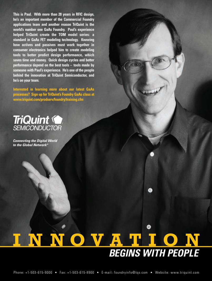
This is Paul. With more than 28 years in RFIC design,he’s an important member of the Commercial Foundryapplications team and another reason TriQuint is theworld’s number one GaAs Foundry. Paul’s experiencehelped TriQuint create the TOM model series: astandard in GaAs FET modeling technology. Knowinghow actives and passives must work together inconsumer electronics helped him to create modelingtools to better predict design performance, whichsaves time and money. Quick design cycles and betterperformance depend on the best tools – tools made bysomeone with Paul’s experience. He’s one of the peoplebehind the innovation at TriQuint Semiconductor, andhe’s on your team.
Interested in learning more about our latest GaAsprocesses? Sign up for TriQuint’s Foundry GaAs class atwww.triquint.com/prodserv/foundry/training.cfm
TriQuint 6_08 CS Ad 5/14/08 3:40 PM Page 1

Compound Semiconductor June 2008 compoundsemiconductor.net 1
Compound Semiconductor’s circulation figures are audited by BPA International
C o n n e C t i n g t h e C o m p o u n d S e m i C o n d u C t o r C o m m u n i t y
induStry
Headline News: Taiwanese giants turn sights on LEDs…RFMD abandons transceiver development efforts…End of the line for Tempe GaAs wafer fab.
The Month in RFICs: Sprint sets the stage for WiMAX rollout…Anadgics soars on record quarterly sales…Bankrupt Caracal confident of buy-out…Cobham targets M/A-COM defense.
The Month in HB-LEDs: Reactor demand buoys Aixtron, Veeco…Analyst tips bright LEDs for notebook rout.
The Month in Optoelectronics: Emcore pockets first real CPV revenue…Bookham and IPG take on output challenges…Arasor holds on for laser take-off.
Portfolio: Aixtron sails through credit jitters After a year in which the credit crunch took its toll on the global financial markets, deposition equipment vendor Aixtron has maintained its position as the best-performing stock in the compound semiconductor basket.
5
6
8
10
12
teChnology
Device Design: Multi-faced LEDs introduce more color Color-converting phosphors hamper the efficiencies of white LEDs. But this can be avoided by switching to quantum-well growth on multiple facets, say Mitsuru Funato and Yoichi Kawakami from Kyoto University.
Osram explores the route to high-performance greens: Why are green LEDs so inefficient? Is it poor carrier injection, high Auger loss, strong internal fields, or poor material quality, asks Osram’s Matthias Peter.
Product Showcase/Suppliers Guide LEDs
III-V solar states its performance case: Looking out of the window on the train from Madrid to Seville, you might see a phalanx of solar panels in a key test plant for compound semiconductor-based energy production. With sites like this becoming increasingly common, the concentrating photovoltaic industry met in Madrid at the CPV Today summit, and Andy Extance joined them.
Hall sensors have the power to deliver unforgettable memory: Hall sensors are incredibly versatile devices. They can analyze the constituents of mining samples, form accurate magnetometers and team up with tiny magnets to create a novel magnetic memory that retains its information when the power is switched off, says Micromem’s Steven Van Fleet.
Ultra-fast VCSELs promise to turbocharge chip communication: The copper interconnects that route chip-to-chip data transfer are reaching their speed limit. But this looming bottleneck can be overcome by switching to ultra-fast VCSELs with tiny threshold currents, say Yu-Chia Chang and Larry Coldren from the University of California, Santa Barbara.
Research Review: Electroluminescence exposes subcells…InGaAs laser breaks into telecom territory…Voids aid AlN formation.
14
16
19
21
25
29
32
Main cover image: Blue LEDs based on InGaN are far more efficient than green ones based on the same material. Why is this and how are companies like Osram trying to solve the problem? See p16. Credit: BridgeLux.
June 2008V o l u m e 14n u m b e r 5
Cooling offReceiver modules help cool down III-V cells from the powerful solar irradiation that they receive in CPV, and also boost Emcore’s potential revenues. p10
In the greenOsram employs its ThinGaN technology in small, medium and large green LEDs for video walls, LCD screens and color projection systems. p18
EmC
OR
E
CSJun08Contents.indd 1 20/5/08 14:58:54

compoundsemiconductor.net June 2008 Compound Semiconductor2
e d i t o r i a l
Editor Michael [email protected] +44 117 930 1013. Fax +44 117 925 1942
Features editor Richard [email protected] +44 117 930 1192
Reporter Andy [email protected] +44 117 930 1007
Senior sales executive David [email protected] +44 117 930 1032. Fax +44 117 920 0977
Business development manager Rosemarie [email protected] +1 215 627 0880. Fax +1 215 627 0879
Sales executive Paul [email protected] +1 215 627 0880
Circulation manager Claire [email protected] +44 117 930 1165. Fax +44 117 920 0984
Publisher Nicola GulleyProduction Louise UnwinAd production Mark TrimnellArt director Andrew GiaquintoTechnical illustrator Alison Tovey
SubscriptionsAvailable free of charge to qualifying individuals working at compound semiconductor fabs and foundries. For further information visit compoundsemiconductor.net/subscribe. Subscriptions for individuals not meeting qualifying criteria: individual £95/$174 US/€142; library £209/$378 US/€305. Orders to: Compound Semiconductor, WDIS, Units 12 & 13, Cranleigh Gardens Industrial Estate, Southall, Middlesex UB1 2DB, UK. Tel +44 208 606 7518; Fax +44 208 606 7303. General enquiries: [email protected].
9835 average total qualified circulation**December 2007 BPA audit statement
Editorial boardMayank Bulsara Atlas Technology (USA); Andrew Carter Bookham Technology (UK); Jacob Tarn OCP/Gigacomm (Taiwan); Ian Ferguson Georgia Institute of Technology (USA); Toby Strite JDSU (USA); Mark Wilson Freescale (USA); Dwight Streit Northrop Grumman (USA); Joseph Smart Crystal IS (USA); Colombo Bolognesi Swiss Federal Institute of Technology (Switzerland); Shuji Nakamura University of California at Santa Barbara (USA)
©2008 IOP Publishing Ltd. All rights reserved.
US mailing information: Compound Semiconductor (ISSN 1096-598X) is published 11 times a year for $174 by IOP Publishing, Dirac House, Temple Back, Bristol BS1 6BE, UK. Periodicals postage paid at Middlesex, NJ 08846. POSTMASTER: send address corrections to Compound Semiconductor, c/o PO Box 177, Middlesex, NJ 08846. US agent: Pronto Mailers Association Inc, 200 Wood Avenue, PO Box 177, Middlesex, NJ 08846.
lights out in tempe
Blue Photonics Inc 23EpiNova GmbH – III/V-Epitaxial Solutions 15Honeywell Electronic Materials CS 3Instrument Systems GmbH 15Jiangsu Nata Opto-Electronic Materials Co. Ltd 9Lake Shore Cryotronics Inc 19Laser Photonics LLC 7
Riber 8SAFC Hitech OBCSEMI IBCSeoul Semiconductor Co. Ltd 20Spire Semiconductor LLC 11Structured Materials Ind Inc 23Tecdia 24TriQuint Semiconductor IFCVeeco 4
Advertisers’ Index
When he delivered his company’s latest financial results on April 22, Skyworks Solutions’ CEO David Aldrich said that he was expecting more consolidation among the manufacturers of GaAs RF chips and components.
Aldrich was right. Within a couple of weeks, Freescale Semiconductor said that it would close its historic CS1 GaAs
fab in Tempe, Arizona. And a few days later Tyco Electronics revealed that it was selling off M/A-COM. Given that Skyworks had acquired Freescale’s GaAs power amplifier business in late 2007 (although not the Tempe fab), Aldrich no doubt had a heads-up on developments in Arizona – but the closure of CS1 did not come as much of a surprise.
Back in the day, Tempe was one of the world’s key compound semiconductor facilities. So where did it all go wrong?
People will have their own theories, but let’s look at some of the history. Motorola opened the fab in 1991 – when mobiles were nearly as big as your head and RF Micro Devices was a fabless three-man start-up. In
June 2000 Tempe became one of the first GaAs fabs to make the transition from 4 to 6 inch wafer production and Motorola boasted that it was the largest RF GaAs facility in the world.
Despite the unfolding technology bust, the following year saw further expansion and the much-heralded, but unsuccessful, development of large-area GaAs-on-silicon material.
Up until then, Motorola’s view was that owning a GaAs facility was crucial for it to maintain a technological lead in RF components for its fast-growing cell phone handset division, which the company is now best known for globally. But that strategy soon changed. The Tempe fab was part of Motorola’s semiconductor products division, a business unit that was increasingly seen as a high-cost impediment to the parent company’s recovery from the post-millennial hangover, rather than a valuable asset.
So, in 2004 Motorola begat Freescale. But despite the close relationship with its parent company and the crucial role that RF components played in Motorola phones, GaAs didn’t seem to be a priority. Freescale’s market share in power amplifiers slipped, and by the time a private equity group acquired the spin-off in late 2006, the writing was on the wall for Tempe.
Michael Hatcher Editor
“Tempe was one of the world’s key compound semiconductor facilities.”
CSJun08Leader.indd 2 20/5/08 15:32:41

the right fit
Contact Honeywell for solutions to your puzzle…visit www.honeywell.com/sm/em or call 1-408-962-2000.
© 2007 Honeywell International Inc. All rights reserved.
With the right investments in the right places at the right time, we’re uniquely positioned to help you make the connection from idea to product success.
Honeywell’s ongoing research and development in chemistry,
metallurgy, and the processes that bring them together—from
our new packaging R&D facility in Spokane, Washington, to our
technology center in Shanghai, China—ensure that wherever challenges arise, we’ll continue
to create solutions that solve them. And as a partner to most of the top semiconductor
houses worldwide, our technology portfolio is consistently at the forefront of invention,
empowering the global leaders of innovation. Honeywell Electronic Materials—bridging
the path to accelerated success.
Right Fit-CS-Sept07.indd 1 8/13/07 11:15:10 AM

WORLD CLASS PRODUCTIVITY — HIGH YIELD WITH HIGHEST CAPACITYTogether, we’re going places. The soaring demand for HB-LEDs requires MOCVD systems engineered for the highest levels of throughput and uniformity — and that’s just what Veeco MOCVD delivers. Our proprietary TurboDisc® technology sets the global standard for non-stop productivity: higher capacity reactors, automated carrier transfers that let you run continuously under vacuum for long periods of time, plus an advanced chamber design and RealTemp® temperature control features to help improve process uniformity. Our K-Series platform is the most modular in the industry, so you can meet changing market demands and protect your capital investment. As you ramp up to your highest level of production, Veeco MOCVD is your fi rst and only stop. For more information, visit http://www.veeco.com/turbodisc1
Veeco MOCVD. Non-stop productivity. Non-stop profi ts.
K465 GaN MOCVD System
vco0055_MOCVD_Ad_cs_D9.indd 1vco0055_MOCVD_Ad_cs_D9.indd 1 5/7/08 12:55:19 PM5/7/08 12:55:19 PM
Compound Semiconductor June 2008 compoundsemiconductor.net 5
Indus try H e a d l i n e n e w s
L E D M a n u fa c t u r i n g
RF Micro Devices is to cease development of transceivers for next-generation hand-sets and sell off its GPS solutions business, reducing its headcount by 350 employees.
The GaAs chip maker estimates that this will save $75 million annually, largely from the decision not to spend research resources on development for broadband wireless transmission protocols, like wideband CDMA, long-term evolution and WiMAX.
Although the move will cost $40 million–$50 million in restructuring charges, RFMD should begin to reap the full financial bene-fit by the end of 2008. The Greensboro, NC, company will refocus these resources on its more profitable compound semiconductor RF components businesses.
“[Transceivers] hid the amounts of money
we’re making in other parts of the business,” said Bob Bruggeworth, RFMD’s CEO. “We said given the amount of money we’re spending on transceivers, we’d be better off spending that in other areas, where we’ve demonstrated that we get better returns, without the uncertainty and risk.”
For the time being RFMD will con-tinue to sell transceivers, so the company expects minimal impact on its overall sales. Indeed, it still expects to see its Polaris 2 and Polaris 3 transceiver modules feature in handsets that are yet to hit the market.
But the rapid pace of wireless technology development suggests that customers will stop buying RFMD’s transceivers within three years. Development of integrated front ends will continue, focusing on GaAs, rather
than transceivers, for future handsets.The shift in strategy came on the back of
a $31.6 million loss posted by RFMD in the closing quarter of fiscal year 2008, a figure that compared badly with the $21.4 million profit that it made in this period last year.
Bruggeworth anticipates that the strategic shift will deliver a more profitable company. He describes the decision to drop transcei-vers as “a very significant event that posi-tions RFMD to deliver the largest increase in profitability in our company’s history”.
Investment analyst John Lau from Jef-feries and Company says that the company should now be much more efficient. “We believe this is one of the most fundamental shifts in product focus for RFMD and will lead to greater profitability going forward.”
One of the compound semiconductor indus-try’s best-known GaAs wafer fabs is to cease operations, with the doors set to close at Free-scale’s Tempe, AZ, 6 inch wafer facility.
Approximately 100 staff working at the site, more commonly known as CS1, were told about the closure on May 12. Freescale
says that these employees will be offered severance packages and invited to apply for jobs elsewhere at the company.
The closure has been on the cards since the sale of Freescale’s high-volume handset power amplifier business to Skyworks Solu-tions in October last year. “Following that announcement we engaged in efforts to sell the facility,” a Freescale spokesperson told Compound Semiconductor. “None of these discussions led to a sale agreement.”
Subsequent to the Skyworks deal, the
remaining employees had been working on comparatively low-volume GaAs product lines for which Freescale will now outsource wafer fabrication to its foundry partners.
The 38,000 ft2 fab was set up in 1991 by Motorola and was one of the first GaAs facilities to move to 6 inch production.
Freescale had already pulled the plug on some innovative research into III-V transis-tors for logic applications, although it is still believed to be pursuing GaN technology for use in wireless base stations.
c o M p a n y s t r at E g y
fa b c L o s u r E
The world’s largest dedicated semiconduc-tor foundry may join one of the world’s top-three thin-film transistor LCD panel makers in moving into compound semiconductors.
AU Optronics and Taiwan Semiconduc-tor Manufacturing Company (TSMC), both of whom make billions of dollars in annual revenues, are looking at breaking into the LED business for future growth.
In a statement to the Taiwan Stock Exchange on April 25, LCD maker AU Optronics (AUO) said that it would invest NT$1.5 billion ($49.3 million) in an LED subsidiary. AUO representatives told Com-pound Semiconductor that the subsidiary, to be called Lextar Electronics, will manu-facture products from the LED chip level through to LCD backlighting units.
Similarly, TSMC, the silicon chip maker
that claims half of all dedicated foundry revenues globally, is looking at LEDs to supplement its core business. Specifically, the company’s “special projects” organiza-tion, headed by Kenneth Kin, is looking at production of light emitters as an option within its ongoing revenue growth plans.
“TSMC is evaluating many new technol-ogies and businesses, and LED is one of the areas that we are looking at,” a spokes-person for the company said.
However, TSMC denied previous reports that it already has a direct relationship with LED maker BridgeLux. TSMC does have close links with a venture capital com-pany called VentureTech Alliance, which recently led a $30 million fund-raising round in California-based BridgeLux. However, the Taiwanese foundry says that
this is where the relationship ends.BridgeLux itself confirmed that position,
as did Bob Walker, who was BridgeLux’s CEO until July 2007. Prior to joining the firm, Walker was also a venture capital-ist focusing largely on LED technology investments in Taiwan. As such, he is not surprised to hear that TSMC is looking seri-ously at a move into LEDs.
“I’m certain that they’re always thinking [about] how they can grow beyond the sili-con manufacturing that they have today,” Walker said. “I think they’d be foolish not to think about LEDs.”
However, Walker poured cold water on any direct link with BridgeLux: “Bridge-Lux’s foundry partner historically has been Epistar,” he said, “so I don’t think there’s any relationship with TSMC.”
taiwanese giants turn sights on LEDs
RFMD abandons transceiver development efforts
End of the line for Tempe GaAs wafer fab
CSJun08Headlinenews5.indd 5 20/5/08 14:25:21

compoundsemiconductor.net June 2008 Compound Semiconductor6
Indus try T h e M o n T h i n R F i C s
B r o a d B a n d w i r e l e s s
GaAs RFIC manufacturer Anadigics regis-tered a record $74.4 million in sales in the first quarter of 2008, up 50% on the same period in 2007, and up 10% on the seasonally strong holiday quarter prior to it.
Despite posting a relatively modest profit of $3.9 million ($9.2 million excluding stock compensation expenses) on its highest-ever quarterly sales, investors swarmed to the stock, with Anadigics’ share price rising by around 25% and maintaining that increase.
This was largely because revenue and profit outstripped expectations, as Anadigics focused on its higher-end, more profitable products while expanding its manufacturing capacity without any apparent glitches.
CEO Bami Bastani said that 2008 had got off to a great start, adding that Anadigics’ GaAs wafer fab had “run fabulously, like a smooth engine”, despite the challenges of increasing capacity to meet demand.
The company is now striving to add more flexibility to its manufacturing strategy to meet the expected future increases in demand. As well as adding personnel and capacity in Warren, NJ, Bastani is aiming to have a foundry partner in place and manu-facturing in volume by the end of 2008.
That should help Anadigics to meet demand prior to the opening of its own new fab in China, which is currently being con-structed and is now expected to come online in the second half of 2009.
Of Anadigics’ rivals in the GaAs business, Skyworks Solutions also enjoyed a positive quarter, with sales of $202 million and an $18.6 million profit beating predictions. The
Woburn, MA, chip maker believes that it has gained market share, and CEO David Aldrich predicted – correctly, given the sub-sequent closure and sale of fabs belonging to Freescale and M/A-COM – that more con-solidation in the industry was imminent.
TriQuint Semiconductor saw a mar-ginal dip in sales from the holiday quarter, although revenues are expected to bounce back in the current quarter as the Oregon-based company assimilates WJ Commu-nications. TriQuint also revealed that its GaAs MMICs are being used in a new gen-eration of military radar systems that will be deployed on the ground in war zones.
The so-called EQ-36 counterfire target acquisition systems, which are now in devel-opment under Lockheed-Martin’s direction, can rapidly scan the entire sky for enemy fire, whereas current radars only scan for such attacks in a single direction.
Caracal, the Pittsburgh-based manufacturer of SiC substrates and epiwafers, has filed for bankruptcy. The company lost out to rival suppliers when the Office for Naval Research slashed the overall spend on SiC development in its latest research funding.
However, it is confident of finding a buyer
to take on its advanced technology and maintain a semiconductor manufacturing presence at its Ford City, PA, location. CEO Andy Chomos told Compound Semiconduc-tor that Caracal had filed for “ Chapter 7” bankruptcy on April 21.
This means that Caracal wants to carry on as a producer of SiC wafers, but that it intends to trade under a different owner. Having held talks with a number of prospective buyers, Chomos said he was “very optimistic” that a deal with a larger semiconductor materials
or device company would be struck.TranSiC, the Swedish developer of SiC-
based semiconductor devices and compo-nents, has released engineering samples of a component that combines a 1200 V, 6 A BJT transistor with a Schottky diode. “We are seeing interest from companies active in the development of power electronic systems for hybrid electric vehicles,” said CTO Martin Domeij. “These customers are looking for voltage ratings in the range 900–1200 V and chip currents exceeding 10 A.”
F i n a n c i a l r o u n d - u p
w i d e- B a n d g a p e l e c t r o n i c s
US communications giants Sprint and Clearwire have breathed new life into their WiMAX strategy, which had been thrown into disarray after plans fell through last November. Now, five major investors are backing a US rollout of networks and services led by Sprint, to the tune of $3.2 billion.
These investors include long-time WiMAX protagonist Intel, along with fel-low big-hitters Google, Time Warner Cable, Comcast and Bright House Networks.
Between them they will sink $3.2 billion into a “new” Clearwire company, with Intel investing $1 billion of that total through its Intel Capital investment unit in exchange for an approximate 7% share in the business. Sprint will be the majority shareholder.
Tom Hausken, a market analyst at Strat-egies Unlimited, said of the announcement: “It can only be good news for the WiMAX
development. Anything that moves it for-ward reduces uncertainty, which is good for the whole supply chain.”
For Anadigics, Intel’s involvement looks like good news because it is already a key purchaser of Anadigics power amplifiers (PAs), which are used in the successful line of “ Centrino” chip sets for Wi-Fi applications.
According to Jefferies & Co invest-ment analyst John Lau, who covers Intel, Anadigics and RFMD stocks, Anadigics is already shipping production orders of mobile WiMAX PAs to Samsung in support of the Sprint/Clearwire rollout.
Meanwhile, RFMD has Motorola on board as a significant customer for WiMAX through its “multimarket products group”, much of which was acquired via last year’s take-over of Sirenza Microdevices.
Although WiMAX technologies are
already being deployed around the world, the anticipated scope of the Clearwire pro-ject sets it apart, with the company target-ing a network capable of serving between 120 million and 140 million people in the US by the end of 2010.
Craig McGraw, chairman of Clearwire, and the man viewed as the force behind the $3.2 billion deal, said: “We believe that the new Clearwire will operate one of the fastest and most capable broadband wire-less networks ever conceived, giving us the opportunity to return the US to a leadership position in the global wireless industry.”
Hausken cautioned component suppliers to view the deal as “one data point”, however: “It’s good news, [but] wireless is notorious for grand visions followed by heartbreak,” said the analyst, who isn’t changing any of his market forecasts just yet.
sprint sets the stage for wiMaX rollout
Anadigics soars on record quarterly sales
Bankrupt Caracal confident of buy-out
CSJun08rfics6-7.indd 6 20/5/08 14:24:17

Compound Semiconductor June 2008 compoundsemiconductor.net 7
Indus t r y T h e M o n T h i n R F i C s
M e r g e r s a n d a c q u i s i t i o n s
UK defense firm Cobham is poised to buy M/A-COM for $425 million, but is not interested in the company’s GaAs and SiGe chip-making operations.
Instead, Cobham’s target is the US com-pany’s suite of microwave and millimeter-wave defense products, which include missile guidance and fusing subsystems, and transmitters and receivers for electronic warfare. It claims that M/A-COM is cur-rently the biggest OEM supplier of micro-wave defense subsystems in the world.
The deal to buy M/A-COM from current owner Tyco Electronics is due to be com-pleted in the second half of 2008. Cobham then plans to sell the non-defense business “for a price that supports the business case” around three months later. This segment currently comprises around 60% of M/A-COM’s total annual revenue.
“A lot of M/A-COM’s commercial busi-ness is foundry products,” said Allan Cook, Cobham’s CEO. “We have experience in buying these components – [but] we have no experience of design and manufacture.”
More precisely, the commercial business sells semiconductor devices and compo-
nents for wireless communications, inclu-ding cellular base stations and WiMAX infrastructure, and RF identification com-ponents for inventory management. “We don’t have the capability to make the most of them,” Cook admitted.
Separating the defense and commercial business will demand a division of the Lowell, MA, site where M/A-COM’s GaAs fab is currently situated. This is likely to see the Lowell-based defense functions relocate, possibly to an existing Cobham address.
The defense company says that it has not yet decided whether to sell the whole com-mercial business together or split it into pieces, but is confident that it will be done quickly. “Based on the encouraging level of interest believed to have been expressed during Tyco Electronics’ auction, Cobham anticipates that this can be divested exped-itiously,” the company said.
Cobham says that it values M/A-COM’s defense business highly and will now pump in more cash than had been the case at Tyco, where it was a “non-core business”.
“We’ve known M/A-COM for many years and tracked it very carefully,” Cook said.
Untitled-3 1 12/3/08 14:25:20
Cobham targets M/A-COM defense
…AXT deals with Olympic disruptionFremont, CA, substrate vendor AXT’s sales of $19.6 million were up 11% sequentially as key customers increased purchases to support mobile handset and solar-energy applications. AXT posted a net profit of $2 million for the quarter, up from $1.6 million previously. The company is also stockpiling materials in advance of the Olympic Games in Beijing this summer, because the local authorities in the country where AXT manufactures its semiconductor wafers will place heavy restrictions on the transport of goods while the Games take place.
…Bede off to the MedIsraeli firm Jordan Valley Semiconductors has taken over X-ray metrology specialist Bede, after the UK firm went into bankruptcy administration at the end of March. “The acquired technology will fit into our product line almost seamlessly and will strengthen Jordan Valley’s position as the market leader in X-ray metrology,” commented Isaac Mazor, Jordan Valley CEO.
…Skyworks in TV phoneNumber-two mobile handset maker Samsung is using front-end modules and power amplifiers from Skyworks Solutions in its latest phones, which are designed for mobile TV applications. Samsung’s P960 Slider phone supports both European mobile TV technology standards and the new open mobile alliance broadcast protocol.
…SiGe hits 250 millionSiGe Semiconductor has shipped more than 250 million integrated circuits as it enjoys success in the RF front-ends of wireless consumer devices. The Canadian company reported 40% year-over-year sales growth.
…RFMD goes for WiMAXRF Micro Devices has released a high-linearity amplifier operating at 5 GHz designed specifically for use in WLAN and WiMAX consumer premises equipment, access point and base transceiver station applications. The InGaP HBT amplifier is optimized for either the final or driver stage in WiMAX equipment.
From our newsfeed…visit compoundsemiconductor.net for daily news updates
CSJun08rfics6-7.indd 7 20/5/08 14:24:34

compoundsemiconductor.net June 2008 Compound Semiconductor8
Indus try T h e M o n T h i n h B - L e D s
E q u i p m E n t s a l E s
MOCVD equipment vendor Aixtron received 785.5 million ($132.5 million) in orders during the first quarter of 2008, more than double the equivalent figure for 2007, as CEO Paul Hyland suggested that the current strong demand cycle was reaching its peak.
The latest figure represented a slight drop from the 786.9 million order intake of the prior quarter, as the German firm’s total order backlog swelled to 7157 million.
“As expected, we have seen some evi-
dence of softening in inquiry levels, which leads us to believe that we are at the apex of the current demand cycle,” said Hyland. But he added that Asian LED makers remain bullish on display backlighting and general illumination, suggesting that any slackening-off period will be brief.
“I don’t expect it to be a deep pause, nor do I expect it to be very long,” Hyland said, adding his belief that 2008 would repre-sent one of the most successful years in the
company’s 25-year history, and reiterating 2008 sales guidance of up to 7300 million. Only a further 750 million of orders that are deliverable this year are needed to hit the 7270 million lower end of its annual target.
In recent quarters, Aixtron has seen increasing requests for multiple reactors delivered regularly over a scheduled period. The company only recognizes orders as being official when it has received a deposit, and it does not always receive deposits for all of the reactors ordered at the beginning of such a timetabled deal. This hidden order backlog therefore adds another level of con-fidence to Hyland’s outlook.
Meanwhile at Veeco, which ranks second to Aixtron in terms of MOCVD equipment market share, sales of epitaxy systems near-doubled as the US company reported much-improved financial results for the opening quarter of 2008.
What the Plainview, NY, company now describes as its “LEDs and solar” division, delivered $42.1 million in sales for the three months up to March 31 – equivalent to 41% of Veeco’s total revenue of $102 million.
These sales represented a 90% increase on this division’s perform ance in the opening quarter of 2007, thanks to growing demand for tools from high-brightness LED manu-facturers, and acceptance of the company’s latest production equipment.
Veeco CEO John Peeler highlighted customer field acceptance of the high-throughput K-465 GaN MOCVD system as an important milestone. He said that with a production capacity of more than 200 LED wafers each day, the tool delivered superior throughput compared with similar epitaxy equipment from its key competitor.
Aixtron previously stole a march on Veeco with its early introduction of high-throughput MOCVD systems. But Peeler believes that the K-Series tools will be able to close the gap by recapturing some market share from its German rival.
“It’s been a good quarter – our new K-465 system saw acceptance from all of its early customers,” said the CEO.
Peeler expects bookings from LED manu-facturers to continue tracking up in the short term, seeing no sign of slackening demand yet. “We have a strong funnel,” he said. “We have seen strong bookings for around two years and there is no sign of a slowdown. [Eventually,] we expect to see a demand cycle emerge, but that hasn’t happened yet.”
Reactor demand buoys aixtron, Veeco
Untitled-4 1 15/5/08 14:09:19
CSJun08hbleds8-9.indd 8 20/5/08 14:23:06

Compound Semiconductor June 2008 compoundsemiconductor.net 9
Indus t r y T h e M o n T h i n h B - L e D s
M a r k e t r e p o r t
High-brightness LEDs will have almost completely taken over from cold-cathode fluorescent lamps (CCFLs) in the backlight function of notebook PC screens within five years. That’s according to analyst Sweta Dash from market research firm iSuppli.
Dash reckons that the much lower power consumption and the absence of mercury in LEDs will increasingly outweigh their higher cost compared with CCFLs, which still dominate in all large-scale LCD back-light applications. By 2012, he says that this trend will culminate in a 90% market share for LEDs in notebook PC displays.
Notebook PCs have always been the obvious large-LCD application for LEDs to penetrate because power consumption is an important feature in portable appliances.
At the moment, however, CCFLs remain the dominant technology, with Dash esti-mating that only 4.7% of notebook PCs manufactured in the closing quarter of 2007 featured LEDs in their display backlights, and just 2.8 million notebook PCs with LED backlights shipped in the whole of 2007. But this year will mark the turning point, with an expected six-fold increase in shipments.
“In the future, as the cost differential
between LED and CCFL backlights nar-rows, LED-based notebook PC panels will gain market share – due to their thinner form factor, lower power consumption and lack of mercury content,” said Dash.
According to Dash’s calculations, a typ-ical 13.3 inch notebook PC screen fitted with white LEDs uses up to 20% less power and is 40% thinner and 20% lighter than a CCFL-based equivalent. But these design advant ages come at a cost: red-green-blue LED solutions remain much more expensive than CCFL backlights, commanding a price premium of up to $80. White LEDs, which are more suited to the smaller displays, are much more competitive, adding a cost pre-mium of only $25 to the PC, says Dash.
Analyst tips bright LEDs for notebook rout
…Mitsubishi eyes white LEDsMitsubishi Chemical has acquired Mitsubishi Cable’s UV-LED assets, which it will combine with its own expertise to break into the white-LED market. These UV LEDs will now be integrated with Mitsubishi Chemical’s phosphor and high-durability sealant manufacturing knowledge, with the intention of producing white-LED packages by 2010. Sales of the individual high-power UV LEDs, UV excitation phosphors and sealants are targeted for launch in 2009.
…Epistar signs on with NeumarkGiant Taiwanese LED maker Epistar is the latest chip manufacturer to agree a licensing deal with Columbia University professor Gertrude Neumark Rothschild.
…Nichia and Seoul back in courtJapanese LED maker Nichia has reignited its ongoing legal spat with Korean rival Seoul Semiconductor by filing an action against
Seoul’s Japanese subsidiary in Tokyo. Nichia says that a raft of Seoul’s white LEDs infringe its Japanese patent 3,900,144, and is seeking monetary damages.
…Fox Group issues licenseCanada-based LED maker The Fox Group has signed a non-exclusive license with an unspecified European company allowing the firm to use technology covered in its SiC crystal growth patents. The Fox Group is instead focusing its efforts on UV-LED development.
…Oxford names new TDI chiefOxford Instruments has appointed Bernard Scanlan, previously the operations director of its nanoscience division, as general manager of its new Technologies and Devices International (TDI) subsidiary. TDI, a specialist in hydride VPE growth of LED structures, is hoping to begin serial production of the reactors by the end of the year.
From our newsfeed…visit compoundsemiconductor.net for daily news updates
Fujitsu is known as a maker of laptops with impressive displays, and its P8010 notebook PC is one of the latest models to feature LED backlights.
FUJI
TSU
CSJun08hbleds8-9.indd 9 20/5/08 14:23:32

compoundsemiconductor.net June 2008 Compound Semiconductor10
Indus try T h e M o n T h i n o p T o e l e c T r o n i c s
P h o t o v o lta i c s
Capacity constraints are putting the brakes on the rapid expansion of Bookham’s tun-able laser manufacturing and delaying its progress to profitability.
In the first three months of 2008, tun-able products accounted for 16% of the company’s $59.7 million revenue, jumping from only 2% of total revenue one year ago. Although Bookham’s 3 inch InP fab in Caswell, UK, is coping well, it seems back-end processing will stop the product line from continuing its exponential growth.
“Tunable is turning into one of our chief product lines, now and for our future,” emphasized Alain Couder, Bookham’s CEO. “In the June quarter we expect a slowdown in the revenue growth, but we are doing everything that we can to meet our customers’ growing demand.”
This restriction means that Bookham is predicting a third consecutive quarter of total sales in the region of $60 million. Net loss in the most recent quarter was $5.2 million, only a slight improvement on the $5.4 mil-lion loss recorded in the previous quarter.
Bookham will use the current quarter to cut costs by completing the move of manu-facturing operations that are currently in San Jose, CA, to Shenzhen in China. The company is also in the process of moving 40% of its total raw material supply to Asian sources, although benefits from this to date have been offset by currency fluctuations.
Even though it represents Bookham’s key hope for the future, the tunable products’ profit margin is lower than the company average. Thanks to its ongoing cost-cutting efforts, Bookham estimates that a return to unconstrained growth in tunables will coincide with much improved profitability for this line and the company overall.
“We believe that continued revenue growth and margin improvement will result
in a transition to positive cash flow before the end of the calendar year,” Couder said.
In contrast, IPG Photonics solved its laser
production problems on its way to another large increase in sales and growing profit for the opening quarter of 2008.
The US company – which dominates the high-power fiber laser business – is still ramping up its manufacturing out-put, although it has largely completed its capital expenditure on this front. The ramp included the purchase of two MBE systems from Veeco for its chip manufacturing facil-ity in Oxford, MA, a little over a year ago.
Referring to problems in late 2007, CFO Tim Mammen declared that IPG had now “dealt with all of those yield issues” and that the capacity expansion would be completed in the third quarter of this year.
IPG registered sales of $52.9 million for the period, up 27% on the first quarter of 2007. Net income of $8.1 million was up 23% year-on-year, despite a sharp increase in litigation costs.
D i o D e l a s e r fa b r i c at i o n
Emcore’s terrestrial solar sales rocketed 10-fold in the first fiscal quarter of this year, but continued expansion of its solar division has added to the company’s losses. Although the Albuquerque, NM, company sold $4.4 million of concentrator photovol-taic (CPV) products in the first three months of 2008, it was hit with one-off charges of $2.3 million from setting up a CPV systems manufacturing unit, and $1.5 million from reorganizing the GaAs-based solar-cell fab.
An overall fab investment of $9 million has boosted capacity by 35%, which will support the company’s satellite solar-cell business, in addition to 250 MW of annual terrestrial production.
“We have a fleet of nine reactors in the installation,” said Hong Hou, Emcore’s CEO. “A tenth one is on the way and we have a plan to add another two reactors.”
Emcore now predicts that the increased capacity will help push CPV revenues to $15 million in the quarter to June, and $30 million in the quarter to September. The company-wide order backlog increased to $158 million at the end of the quarter from $156 million, in spite of this ramp-up. “Right now we are hand-to-mouth for fab capacity,” Hou commented.
Emcore’s satellite solar sales brought in $14.2 million in the most recent quarter, but
the division also took a $2.5 million hit in exceptional charges arising from contamin-ated wafers, which were received from an undisclosed supplier.
Satellite revenues look set to fall to around $10 million in the next quarter as Emcore waits for confirmation of new contracts. Despite this, the management is confident of the long-term stability of the satellite solar
business thanks to the imminent engage-ment of an additional customer.
Overall, Emcore turned in a $17.5 million net loss in the first three months of 2008, worse than the figure of $14.5 million for the last quarter and $13.4 million for the same time last year.
In spite of this, Hou predicts profitabil-ity in the September quarter, on the basis of anticipated $100 million revenues.
Emcore has added to its solar order pipe-
line by selling directly to a customer of its biggest III-V solar-cell client, after the record deal with Green and Gold Energy attracted adverse speculation (see p12).
The GaAs company has now signed a $28 million supply agreement for cells and receivers with ES System, a South Korea-based CPV system maker. Under the agree-ment, Emcore says, 70 MW of receivers are to be deployed in fully licensed and funded solar farms.
ES System licenses “SunCube” concen-trator technology from Australian company Green and Gold Energy, which previously placed an order for $39 million worth of GaAs cells and receivers from Emcore. Green and Gold Energy markets the Sun-Cube as a robust but lightweight, manufac-turable photovoltaic system with in-built solar tracking capability.
emcore pockets first real cPv revenue
Bookham and IPG take on output challenges
Receiver modules help cool down III-V cells from the powerful solar irradiation that they receive in CPV, and also boost Emcore’s potential revenues.
EmC
or
E
CSJun08Optoelectronics10-11.indd 10 20/5/08 14:20:57
Compound Semiconductor June 2008 compoundsemiconductor.net 11
Indus t r y T h e M o n T h i n o p T o e l e c T r o n i c s
L a s e r D i s p L ay s
Australian optoelectronic company Arasor is continuing to refocus its business towards laser chip manufacture, despite losses forcing it into drastic cost cutting.
Arasor recorded a AUS$16.7 million ($15.6 million) loss on AUS$117 million revenue in 2007. Consequently at its May 15 AGM, the company said that it is “terminating” employees and consultants, closing down locations and exiting businesses to reverse this trend.
These moves are the latest results of a strategy that Arasor started in 2006 to expand upon its basic lithium niobate optics business. The company growth has subsequently centered on an optoelectronics business that has been restricted to lowmargin opportun ities in Chinese and Indian wireless infrastructure. Limited profitability in this area has been worsened by problems with an Indian customer that has resulted in delays in revenues due to Arasor.
Now the optics firm is increasingly pinning its hopes on laser displays, in advance
of Mitsubishi Electric’s US launch of its Laservue television, which is expected in the third quarter of this year.
Arasor has provided Mitsubishi’s light engine suppliers with lasers made by Novalux, whose purchase Arasor completed earlier this year. Former Novalux CEO William Mackenzie has now replaced Simon Cao as CEO of Arasor, although Cao will remain executive chairman “to focus on global strategic initiatives”.
The change of strategy is being aided by a AUS$1.5 million government grant to Arasor’s Bandwidth Foundry subsidiary for the commercialization of laser projection. Arasor says that the funds will help it make the most of the Novalux acquisition and its ongoing joint venture with ZTE International for laser displays. That deal with the investment arm of the Chinese telecoms giant is aiming to establish a new company that will produce 6 million laser light sources and 2.6 million light engines annually by 2010.
Spire Semiconductor, LLC25 Sagamore Park Road, Hudson, NH 03051
T 603.595.8900 F [email protected]
1
2
3
4
5
6
7
Edward D. GagnonGeneral Manager,
Spire Semiconductor
8
to Work with Spire Semiconductor
to Develop Your Next
OptoelectronicsProduct...
8 Reasons
Spire Semiconductor is a complete compound semiconductor fabrication facility dedicated to supporting its customers.
Spire Semiconductor has its own MOCVD III-V and II-VI multi-wafer, multi-reactor capabilities for high volume production requirements.
Spire Semiconductor has a first-class compound semiconductor device fabrication facility with class 100 cleanrooms.
Spire Semiconductor’s engineering staff has extensive experience in material and device design, process development and testing.
You can work directly with Spire Semiconductor’s engineers.
Spire Semiconductor can manufacture your products in volume exclusively for you.
As a pure play foundry, we do not compete with our customers.
Working with Spire Semiconductor will keep you ahead of your competition.
Semiconductor
Arasor holds on for laser take-off
…InP HBT shifts phaseThe ingenuity of GigOptix’s customers has helped it to rebrand an InP transistor for phase-shift keying modulation as used in today’s state-of-the-art optical telecommunications networks. Initially the company’s iT4036 phase delay device was designed for test and measurement in 10 Gbit/s optical communications, but it has found its way into a wider variety of applications. That’s because it can deal with frequencies ranging from direct current up to 12.5 Gbit/s alternating currents – an ability that GigOptix believes may give this HBT a unique place in the market.
…NASA sponsors Kopin solar comebackKopin, Skyworks’ key GaAs HBT supplier, has gained $600,000 from NASA to develop solar cells based on InN quantum dots. The contract is the second phase of a Small Business Technology Transfer grant and includes collaboration with partners at Virginia Tech and Magnolia Optical Technologies. The first phase demonstrated the production of device-quality InN quantum dots, and this phase will see the material embedded in a GaN structure.
…Modulight shoots for the starsSemiconductor laser manufacturer Modulight has been awarded a $1.1 million-plus contract to develop high-brightness pump lasers for the European Space Agency. The two-year deal will see the firm design and engineer models of space qualifiable high-brightness and high-reliability quasi-continuous-wave laser arrays for Earth observation. The lasers will operate in the 800 nm bandwidth range with output powers of more than 200 W, and should be stackable to make combined 1 kW output laser modules.
…VCSEL maker gets $1.3 million kickstartBeamExpress SA, which develops high-speed long-wavelength lasers in conjunction with the Swiss Institute of Technology in Lausanne, has secured $1.3 million in funds from venture capitalist I-Source. The company is an offshoot of BeamExpress Inc, and emerged when its former owner was sold to optical communications firm Neophotonics. The company says that this first funding round will help it to manufacture high-performance VCSELs thanks to its “localized wafer fusion” technology, which can unite GaAs and InP wafers.
From our newsfeed…visit compoundsemiconductor.net for daily news updates
CSJun08Optoelectronics10-11.indd 11 20/5/08 14:21:18

compoundsemiconductor.net June 2008 Compound Semiconductor12
Indus try P o r t f o l i o
You don’t need to be a financial wizard to know what kind of year it has been for bankers. 12 months ago who had even heard of the term “credit crunch”? But through the end of 2007 it had become the headline of choice in newspaper offices around the world.
For the banking sector it has been a nightmare. With the finger of blame pointing squarely at what now looks like borderline insane institutional lend-ing to sub-prime customers clearly out of their finan-cial depth, the fall-out has so far included some huge write-downs, the implosion of US bank Bear Stearns and a hell of a lot of bankers looking for a new job.
But the effects on the wider economy, and on those sectors that are served directly by compound semi-conductor components, are yet to really play out. And while a few CEOs from the industry brought up the subject of an impending slowdown in their recent quarterly financial results, none of them spoke of any direct impact on their sales just yet.
Worries of a slowdown may have weighed down many stock prices, although one key company buck-ing that trend for the second year running is Ger-
man equipment vendor Aixtron. The firm, which holds the lead in MOCVD reactor sales ahead of US rival Veeco Instruments, enjoyed another quarter of “exceptional” order intake in the three months up to March 31, as LED manufacturers continued to invest in equipment needed to supply chips to be used in display backlight applications.
“As expected, we have seen some evidence of soft-ening in inquiry levels, which leads us to believe that we are at the apex of the current demand cycle,” is how Aixtron’s CEO Paul Hyland described the pic-ture. He says that, even if there is a slowdown in sales of MOCVD kit, he does not expect it to last long.
With a net profit of 724.5 million ($37.8 million) in its back-pocket from the first three months of the year, and a huge sales backlog of 7157 million thanks to several quarters of busy order activity, Aixtron’s share price has held up very nicely at a time when the vast majority have headed in the opposite direction.
Between May 2, 2007, and May 9, 2008, shares in Aixtron rose by just over 50%, putting the company at the top of our leaderboard – even taking into account
Aixtron sails through credit jittersAfter a year in which the credit crunch took its toll on the global financial markets, deposition equipment vendor Aixtron has maintained its position as the best-performing stock in the compound semiconductor basket.
S h A r e- p r i c e S u r v e y
Compound semiconductor share-price leaderboard
Rank Company Ticker Share value May 2, 2007 ($)
Share value May 9, 2008 ($) % appreciation Change in
rank
1 Aixtron (Frankfurt) AIX 6.12 9.29 51.80 –
2 Emcore EMKR 4.96 6.71 35.28 +19
3 Rubicon RBCN 17.50* 23.31 33.20 new
4 Cree CREE 19.16 24.85 29.70 +14
5 Triquint TQNT 5.13 6.45 25.73 +2
6 AXT AXTI 3.90 4.77 22.31 +2
7 Skyworks SWKS 6.85 8.28 20.88 –2
8 IQE IQE 15.75 18.11 14.98 –2
9 IPG Photonics IPGP 17.99 19.69 9.45 new
10 Anadigics ANAD 10.59 11.32 6.89 –8
11 Veeco VECO 18.37 18.29 –0.44 +2
12 NASDAQ composite Index 2531.53 2445.00 –3.42 –8
13 Kopin KOPN 3.41 3.09 –9.38 +4
14 Hittite HITT 43.68 38.28 –12.36 –11
15 Bookham BKHM 2.18 1.82 –16.51 +5
16 Endwave ENWV 10.14 7.00 –30.97 –
17 JDSU JDSU 16.64 11.30 –32.09 +2
18 Infinera INFN 19.71** 13.05 –33.79 new
19 Riber (Paris) RIB 1.66 0.97 –41.57 –5
20 RFMD RFMD 6.18 3.35 –45.79 –9
21 Finisar FNSR 3.56 1.38 –61.24 –9*launch price on November 16, 2007; **launch price on June 7, 2007.
Aixtron topped our leaderboard for the second year running, as investors recognized the surge in demand for MOCVD tools required by high-brightness LED manufacturers for applications in larger-format displays. However, if we had included First Solar, the CdTe solar cell specialist, it would have easily topped our chart. First Solar has been one of the darlings of the market over the past year, and registered a near five-fold increase in valuation between May 2007 and May 2008.
SO
UR
CE:
YAH
OO
FIN
ANC
E
CSJun08Portfolio12-13.indd 12 20/5/08 14:19:52

Compound Semiconductor June 2008 compoundsemiconductor.net 13
Indus t r y P o r t f o l i o
the sharp drop after the latest results that suggested investors were wary about Hyland’s assurance of a “soft landing”. Rival Veeco, which is exposed to a wider set of markets than Aixtron, was pegged back on weak performance in sectors outside compound semiconductors. Despite that, its near-flat stock per-formance over the past year made the company a better investment than the Nasdaq composite index, which dropped by just over 3% at the same time.
Herd mentalityWith the usual herd mentality, investors found them-selves a new favorite over the past year – alternative energy companies and “green” technologies. High-brightness LEDs certainly fall into the latter category, and chip maker Cree has ascended our leaderboard rapidly as if to demonstrate that. The company’s stock grew 30% in the past year, enduring a series of sharp peaks and troughs prior to a 15% plunge after its latest results were announced.
Investors appeared worried by Cree’s diminishing profitability, a sharp increase in LED inventory lev-els and what was perceived as a weak outlook for the next quarter. However, a closer look at the company’s results shows that the lower profit compared with the same period last year was largely due to tax benefits registered in 2007. Cree certainly faces challenges as it strives to become known as a lighting company (rather than a humble semiconductor manufacturer), and the acquisition of LED Lighting Fixtures has also hit its overall profit margin slightly.
Significantly, perhaps, Cree’s sales of packaged LEDs exceeded those of its chips for the very first time in the latest quarter. But although LEDs are now starting to find applications in general lighting, it will be many years before Cree can claim to have “obsoleted the light bulb”.
One of the more immediate challenges for Cree is on the patent litigation front, with cases involving BridgeLux, Honeywell and the litigious academic
Gertrude Neumark Rothschild all in the pipeline.Another beneficiary of the trend towards alternat-
ive energy companies is Emcore, which is position-ing itself as two separate companies – one dedicated to solar cells and solar power systems, and the other focused on optical communications components.
A year ago Emcore sat at the bottom of our leader-board after shedding nearly two-thirds of its market value inside one year. Since then, a raft of announce-ments of forthcoming sales of solar cells and systems has helped the stock rally strongly, adding 35%. But that simple analysis hardly tells the story of what has been a roller-coaster ride for Emcore’s shareholders.
In late December 2007, Emcore had spiked up to $15.30, more than three times its May 2007 valu-ation. After a new-year wobble, Emcore’s market value then crashed through the floor in mid-March after the publication of a US investment blog post that tore into the reputation of one of Emcore’s key cus-tomers for solar cells and receivers, and of concentra-tor photovoltaics in general.
While much of that report was inaccurate, not to mention potentially libellous, it appears that some mud has stuck. Emcore, which felt compelled to issue a company statement about the negative post, says that it has asked US government securities regulators to investigate the relationship between the author of the blog in question and what it described as short-selling of Emcore stock at the time.
There’s no word on the outcome of any investiga-tion just yet, but Emcore’s stock is yet to recover any momentum. That’s in stark contrast to First Solar, another maker of solar cells, albeit one that manufac-tures thin-film CdTe on a glass substrate. Over the nine months from May 2007 to February 2008, inves-tors would have seen a near-identical return from each of the two companies. But as Emcore dropped away, First Solar continued to spiral upwards and, if we had included that company in our leaderboard, it would have topped the list by a country mile.
May 20
07
May 20
07
May 20
07
Jun 20
07
Jun 20
07
Jul 20
07
Jul 20
07
Aug 2
007
Aug 2
007
Sep 2
007
Sep 2
007
Oct 20
07
Oct 20
07
Oct 20
07
Nov 20
07
Nov 20
07
Dec 20
07
Dec 20
07
Jan 20
08
Jan 20
08
Feb 2
008
Feb 2
008
Mar 20
08
Mar 20
08
Apr 2
008
Apr 2
008
Apr 2
008
16
14
12
10
8
6
4
pric
e ($
)
agrees 60 MW dealwith Canadian company
completes financialrestatement
receives majororder from Green andGold Energy
negative blogpublished
Michael Hatcher does not own or intend to purchase any of the stocks in this article.
In a roller-coaster ride for Emcore investors, the chip manufacturer’s share price rose just as rapidly as First Solar’s in the second half of 2007, as Emcore revealed details of a number of major supply deals. But after a dip in early 2008, Emcore shed nearly half of its value in just a few days after the publication of a caustic blog that attacked one of its major customers. As this issue of Compound Semiconductor went to press, Emcore’s stock had recovered to $8.38.
So
ur
CE:
YAh
oo
Fin
AnC
E
CSJun08Portfolio12-13.indd 13 20/5/08 14:20:15

compoundsemiconductor.net June 2008 Compound Semiconductor14
Technology D e v i c e D e s i g n
Colored LEDs have one significant drawback – a limited color palette. This stems from the light- generating process, which is governed by the band-gap of the active ingredient.
Fortunately, several options already exist for extending LED spectral emission. The most success-ful method to date is the pairing of a yellow phos-phor and blue InGaN chip to produce a white emitter. This device is already a great commercial success thanks to deployment in general lighting, displays, nanobiotechnology and medicine. However, poor color rendering is common due to weak red and green emission, and large variations in the output color often occur across batches of LEDs due to variations in phosphor emission color.
All of these issues can be overcome by employ-ing phosphor-free designs. Mixing the output of red, green and blue LED chips is one option, and this approach can deliver a high degree of control over the overall color. However, device assembly is tricky and carefully designed external optics are needed to ensure good color mixing.
Monolithic designs ought to be a better solution, and researchers from Nichia in Japan and CNRS in France have already made some progress on this front. They have generated white emission from InGaN LEDs featuring several quantum wells (QWs), each with differing colors. However, because the wells are connected in series, the spectral output of this type of device cannot be adjusted by current tu ning. Instead, the overall emission is dictated by the individual properties of each QW.
A radical design that connects QWs in parallel could overcome this weakness, which is precisely what we have done at Kyoto University in Japan. This breakthrough was achieved by growing the wells on different crystal facets of GaN. Each crystal plane produces a QW with a particular color, due to the differences in the thickness of the well and its indium composition (figure 1).
Our novel LEDs are made by MOCVD growth on sapphire (0001) at 300 Torr. We can form ridge-shaped structures by using processes allied to those employed for epitaxial lateral overgrowth – the widely used technique for cutting threading disloca-tion densities in GaN heteroepitaxial layers. A few microns of GaN are deposited, before SiO2 mask stripes are defined in the [1
–100] direction by plasma-
assisted CVD and photolithography. GaN regrowth forms microstructures containing (0001) and 11
–22
facets along the [1–100] direction. We then deposit
InGaN/GaN three-period QWs and p-GaN cap layers onto these microfacets.
The microfacet’s shape depends on the SiO2 mask dimensions. We initially employed mask openings of 5 and 15 μm for our prototype structures. This pro-duced narrow and wide trapezoidal cross-sections, which we refer to as A and B, respectively (figure 1).
Conventional processingAlthough our device structure is radically different from that of a conventional LED, this does not pre-vent us from employing conventional device process-ing. The photolithography step has been optimized, however, to cater for three-dimensional structures.
Our LEDs are formed by inductive coupled plasma reactive ion etching, which isolates the devices and exposes n-GaN by the removal of a portion of p-GaN and the QWs. Ni/Au and Ti/Al ohmic contacts are deposited on p-GaN and n-GaN, respectively.
Multi-color LEDs result from differences in the indium composition and thickness of the QWs on each of the two facets. The QWs occupy a larger area on the 11
–22 facet than the (0001) facet in A,
and vice versa in B (figure 1). Consequently, emis-sion from the 11
–22 facet QWs dominates the out-
put from A, while the (0001) facet dictates the output from B. The overall spectral output can be adjusted by independ ently varying the drive currents to the two facets because they are connected in parallel.
We have produced a range of multi-color LEDs with various growth conditions and stripe patterns, which have different emission spectra (figure 2). Accord-ing to microscopic luminescence measurements, blue emission is produced from the 11
–22 facet. Yellow
Multi-faced LEDs introduce more colorColor-converting phosphors hamper the efficiencies of commercial white LEDs. But this can be avoided by switching to quantum-well growth on multiple facets, say Mitsuru Funato and Yoichi Kawakami from Kyoto University.
W h i t E E M i t t E r s
p-GaN
(0001)500 nm
1122
n-GaN[1120]
[0001]
[1100]
500 nm(0001)
p-GaN1122
n-GaN
n-GaN
SiO2sapphire 10 µm
Fig. 1. This corrugated structure features narrow and wide trapezoidal cross-sections (A and B, respectively) produced by GaN growth through SiO2 masks. The quantum wells on the 11
–22 and
(0001) facets emit at different wavelengths. The overall color can be adjusted by current tuning.
About the authorsMitsuru Funato is an associate professor in the department of electronic science and engineering at Kyoto University. He is interested in crystal growth and optical/structural properties in wide-bandgap III-nitride semiconductors. Yoichi Kawakami is a professor in the same department at Kyoto University. His research focuses on spectroscopic investigations of light–matter coupling and its application to optical devices.
A B
CSJun08DeviceDesign14-15.indd 14 20/5/08 14:18:39

Compound Semiconductor June 2008 compoundsemiconductor.net 15
Tec hnol ogy D e v i c e D e s i g n
emission comes from the (0001) facets in B, while red results from the (0001) facets in A.
Color mixing of the red, yellow and blue emis-sion creates a white output without the need for any external optics. This has a chromaticity close to that of a “blackbody”. Color temperatures of 4000, 6000 and 15,000 K were produced by varying the A:B ratio and the growth conditions. These color temperatures overlap those of fluorescent lamps (3000–6500 K) and conventional white LEDs (5500 K). Our LED design is also capable of producing pastel colors, such as bluish and greenish white, through careful control of the mask patterns and the growth conditions.
Simulations have revealed that our LEDs have high extraction efficiencies, which result from the three-dimensional structures. This means that additional process steps are not required to boost extraction. It also suggests that the current fabrication process is suitable for high-volume manufacture. However, improvements are needed to our device’s red and green quantum efficiencies before it can take on today’s commercial white LEDs.
We are addressing this goal with a new structure, and results will be presented in the near future. Our devices have the potential to deliver high efficacies, thanks to the absence of phosphors and the incorpor-ation of three-dimensional structures, and we are optimistic that our multifacet LED will be a key device in next-generation solid-state lighting.
Further readingM Ueda et al. 2007 Appl. Phys. Lett. 90 171907.Y Kumagai et al. 2008 Appl. Phys. Exp. 1 045003.M Yamada et al. 2002 Jpn. J. Appl. Phys. 41 L246.
400 500 600 700wavelength (nm)
3.2 2.8 2.4 2.0 1.6
EL in
tens
ity (a
.u.)
photon energy (eV)
A:B = 2:1
2:1
1:1
A: (0001)
B: (0001) RTA, B: 1122
(a) (b)
Fig. 2. (a) Variations in the SiO2 mask pattern produce different white-light color temperatures. (b) A color temperature of 5000 K can be produced when A:B is 1.
Measure all optical and electrical pa-rameters of single LEDs, high-power LEDs and LED modules in conformity to international standards accurately and within seconds. With equipment from INSTRUMENT SYSTEMS – the world leader in LED metrology.
phone +49 89 45 49 [email protected]
WE BRING QUALITY TO LIGHT
LED Test and Measurement
Luminous intensity (candela) Luminous flux (lumen) Dominant wavelength (nm) Color coordinates (x, y, z) Spatial radiation pattern Thermal behavior
Project3 2/10/06 13:40 Page 1
CSJun08DeviceDesign14-15.indd 15 20/5/08 14:19:04
compoundsemiconductor.net June 2008 Compound Semiconductor16
Technology L E D s
Why are green LEDs so inefficient? Is it the result of poor carrier injection, high Auger loss, strong internal fields, or simply poor material quality, asks Osram’s Matthias Peter.
Osram explores the route to high-performance greensThe InGaN-based LED is the linchpin of the LED market. It forms the key ingredient in green and blue emitters, as well as providing the foundation for white LEDs employing yellow phosphors.
Although the first InGaN LEDs were fairly dim, efficiencies have increased by more than an order of magnitude over the last decade, and many of today’s emitters are very efficient. For example, the blue ThinGaN LEDs that we produce at Osram have a wall plug efficiency exceeding 50%. This design can be scaled without additional loss, and has been used to produce 1 mm × 1 mm, 571 mW LEDs.
However, high efficiencies are not universal, and InGaN LEDs operating at longer wavelengths are producing more modest outputs. While UV LEDs can hit internal quantum efficiencies (IQEs) of 80% at low current densities, far lower efficiencies are produced at longer wavelengths. An IQE of less than 30% is typical at 540 nm, and in the red efficiency falls to single digits. Higher drive currents also reduce IQE, particularly at long wavelengths, due to a poorly understood phenomenon known as “droop”.
Red LED makers can circumvent InGaN’s low efficiencies by turning to a different material sys-tem – InGaAlP. This mature quaternary produces highly efficient yellow, amber and red emitters. However, it is incapable of delivering efficient emis-sion at less than 580 nm due to decreases in carrier confinement, which means that there are a range of greenish wavelengths between 500 and 580 nm where neither InGaN nor InGaAlP can be used to make high- efficiency LEDs. It is an area that has been coined the “green gap”. LEDs operating in this region have wall plug efficiencies of less than 20%.
Wall plug efficiencies do not tell the whole story, and are just one method for gauging LED perform-ance. If efficacy, luminous flux (lm) or luminous intensity (cd) is used, then green LEDs get a helping hand because these units of measurement account for the spectral response of the human eye. This is strongest at 555 nm. Measurement of efficacy and luminous flux and intensity show green LEDs in a better light at wavelengths towards the edges of the green gap, but can’t hide the emitter’s weaknesses at around 560 nm (figure 1).
Figure 1 also illustrates the significant contri-bution that an efficient green LED could make to the efficacy of a white-light source formed by red-green-blue (RGB) color mixing. However, the effi-
ciencies of today’s green emitters are so low that the brightest white-light sources are still based on phosphor-converted blue LEDs, even though this design has to contend with a Stokes loss caused by conversion of blue light into yellow emission.
Efficient LEDs emitting near the center of the green gap are needed to raise the quality of white light formed by color mixing (figure 2).
Understanding InGaNImproving green-LED performance is impor-tant, and efforts are underway to obtain a greater understanding of the reasons behind the decrease in InGaN LED efficiency at longer wavelengths. Although explanations are under debate, it is accepted that the major physical changes resulting from the increase in indium content needed to make green LEDs, rather than blue ones, are a shift in lat-tice constant and a shortening of the bandgap.
LED manufacturers produce their devices on sap-phire or SiC. Although this leads to many dislocations and a high degree of strain at the epiwafer–substrate interface, additional growth produces a buffer that is essentially relaxed. The proceeding layers are then strained relative to the GaN lattice constant.
Blue-emitting InGaN quantum wells (QWs) require 15–20% indium content, while their green cousins demand 25–35%. This might not seem a
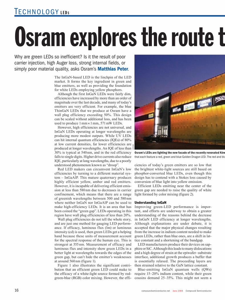
Osram’s LEDs are lighting the new facade of the recently renovated Köwe shopping center in Regensburg. Illumination is provided by 816 modules that each feature a red, green and blue Golden Dragon LED. The red and blue chips have much higher efficiencies than their green equivalent.
OS
rAm
CSJun08OSRAM16-18.indd 16 20/5/08 14:16:56

Compound Semiconductor June 2008 compoundsemiconductor.net 17
Technology L E D s
Osram explores the route to high-performance greens
big difference, but it is. InGaN is plagued with a miscibility gap that makes it difficult to grow thick layers of this ternary on GaN, particularly when the indium content is high. The miscibility gap can drive the creation of two separate InGaN phases and the formation of indium clusters. InGaN can also degrade at high temperatures, such as those used for the growth of p-type material. This hampers band-gap engineering of the active region’s barrier layers, which is needed to optimize carrier transport and improve strain management.
High-quality InGaN is produced by growing layers that don’t exceed the critical thickness – a thickness that leads to material relaxation. It’s easy to determine this value in GaAs/InGaAs and GaAs/AlGaAs, but InGaN is a different matter because it is difficult to detect the onset of additional dislo-cations in a layer that typically has 108 dislocations per cm2. However, there is no evidence that green InGaN QWs actually exceed their critical thickness – X-ray diffraction reciprocal-space maps reveal that green QWs are fully strained, which implies that the critical thickness has not been reached.
Increasing indium content in InGaN QWs streng-thens their internal piezoelectric fields, which in turn reduces the overlap of electron and hole wave functions. This can account for the blue-shift of the emission peaks in conventional InGaN LEDs at
high drive currents. However, reduced wavefunction overlap cannot quantitatively account for the halving of efficiency between green and blue LEDs, or the loss mechanisms for high- indium-content non-polar LEDs driven at high current densities.
Recently, an explanation for InGaN LED losses has been proposed by Fred Schubert’s team at Rens-selaer Polytechnic Institute, which focuses on car-rier injection. In conventional LEDs, carriers have to overcome potential barriers due to band bending, which are caused by the internal piezoelectric fields. Since band bending increases with indium content, this can account for the lower efficiencies in the green and the poorer performance at high currents.
However, theories based on carrier injections – like those centered around piezoelectric fields – cannot explain the drop in the efficiency of non-polar LEDs that are free from internal fields at long wavelengths, such as 470 nm.
At Lumileds, Mike Krames’ research team has been championing Auger loss as the primary cause
1000
100
10
1400
effic
acy
(lm/W
)500450
“cold white”
InGaNInGaAIP
wallplug efficiency
“warm white”
wavelength (nm)550 600 650 700
80%60%40%
100%
“green gap”
10%
20%
0.5
0.0
1.0
1.5
2.0
2.5
400
norm
alize
d in
tens
ity (a
.u)
500450wavelength (nm)
550 600 650 700
warm-white: CRI = 82ultra-white: CRI = 68
RGB-white: CRI = 87RGB-white: CRI = 68
Osram’s LEDs are lighting the new facade of the recently renovated Köwe shopping center in Regensburg. Illumination is provided by 816 modules that each feature a red, green and blue Golden Dragon LED. The red and blue chips have much higher efficiencies than their green equivalent.
Fig. 1. (top) Efficacy values account for the response of the human eye, which peaks at 555 nm. This wavelength is very close to the center of the green gap, a region where InGaN and InGaAlP LEDs are highly inefficient. Fig. 2. (bottom) Most of today’s white-LED sources feature a blue chip and yellow-emitting phosphor. Switching to a red phosphor can improve the color rendering index (CRI), a measure of color quality that assigns an incandescent lamp a value of 100. However, gains in CRI come at the expense of a lower efficacy, due to a higher Stokes loss. This loss can be eliminated by producing white light from the mixing of red, green and blue LEDs, an approach that promises to combine a high efficacy and CRI. However, this scheme is currently held back by the poor efficiency of the green emitters. The green emission wavelength plays a very important role in the CRI of white light, and a shift from 526 to 542 nm can boost that figure from 68 to 87.
CSJun08OSRAM16-18.indd 17 20/5/08 14:17:18

compoundsemiconductor.net June 2008 Compound Semiconductor18
Technology L E D s
of LED droop. This theory explains why current losses are proportional to the cube of carrier den-sity at high currents, and accounts for losses in high-quality non-polar InGaN LEDs. However, the Lumileds’ team has not provided a direct proof for Auger loss and their case rests on the elimination of other theories. The Auger recombination coefficient that the team employs for its calculations is also much higher than that obtained from extrapolations of infrared devices, and other loss mech anisms are probably needed to explain why green LED effi-ciency losses kick in at very low current densities.
None of the theories that have been described above can account for the sharp decline in effi-ciency between blue and green LEDs, which must be partly explained by changes in the material, such as an increase in defects or greater inhomogene-ity in the InGaN layers. Increasing indium content leads to more strain and a rise in point defects. How-ever, it is very difficult to observe these directly, although they have been recently observed in non-polar InGaN QWs by researchers at the Univer-sity of Tsukuba and at UCSB. Inhomo geneities in InGaN QWs have also been seen on several length scales by various methods, inclu ding the atom probe technique employed by Colin Humphreys’ group at Cambridge University.
Although we are still waiting for a “water-tight” explanation for the lower efficiencies of green LEDs, the current lack of understanding has not prevented our community from making substantial progress – green-LED efficiency has shown a 10-fold increase over the last decade. Our company has been part of this success story, and we have made recent advances by studying the performance of various multiple-quantum-well (MQW) structures.
Our efforts have focused on improvements to green MQW structures. To this end, we compared the output of two MQW ThinGaN LED chips at vari-ous operating temperatures: a MQW green emitter, and a color-coded device with a green well on top
of six blue ones. The two-color device was used to evaluate the contribution of the top well to overall electroluminescence. This well utterly dominates at liquid helium temperatures and very low currents, and contributes 70% of the overall output at room temperature and 10 mA current. This means that the high piezoelectric fields within the green wells do not restrict electroluminescence to just the one well. Instead, MQW operation is possible, even for high indium content material. This increases LED effi-ciency and reduces the problems of droop thanks to a lower current density per well.
We went on to improve the epitaxial structure of the two-color LEDs, before fabricating single-color green LEDs that incorporated optimized active regions. These were more efficient than our previous green LEDs at typical and high drive currents, and produced a smaller shift in wavelength with current.
This design is being used in our latest commercial green LEDs, which feature a superior QW structure (see box “Osram’s high-performance greens”).
We will continue to try to eliminate the green gap because pro gress in this direction would sig-nificantly improve the performance and cost of today’s RGB sources. Ultimately, however, it could do something more exciting – it could help to usurp the phosphor-converted blue LED, and provide really high efficacy sources based on RGB modules for applications such as mainstream lighting. l
Further readingS F Chichibu et al. 2006 Nat. Mater. 5 810–816.B Hahn et al. 2007 WOCSDICE 3.K Iso et al. 2007 Jap. J. Appl. Phys. 46 L960.M-H Kim et al. 2007 Appl. Phys. Lett. 91 183507.M Peter et al. 2008 Phys. Stat. Sol. (c) 5 2050.Y C Shen et al. 2007 Appl. Phys. Lett. 91 141101.R Windisch et al. 2007 IEEE Photon. Lett. 19 1041.J Wu et al. 2002 Appl. Phys. Lett. 80 4741. H Yamada et al. 2008 Appl. Phys. Exp. 1 041101.S Yu et al. 2004 Phys. Stat. Sol. 241 2668.
Osram employs its ThinGaN technology in small, medium and large green LEDs. Small chips that are typically 300 μm × 300 μm in size are suitable for video walls. Mid-size chips that are up to 1 mm2 are designed for the backlighting of large LCD screens, and larger chips are targeting color projection systems.
The company’s 255 × 460 μm chips, which are housed in 5 mm radial lamps, produce up to 13.5 mW and 107 lm/W, respectively, at 20 mA and 532 nm. In comparison, the best
blue LEDs produce 31.4 mW at the same drive current, which equates to a wall-plug efficiency of 51%.
At the 1 mm2 size, 531 nm chips produce up to 109 lm and 209 mW at 350 mA with efficacies
of 90 lm/W. At 700 mA a luminous flux of 170 lm is produced at efficacies of up to 65 lm/W. In contrast, the company’s equivalent-sized blue chips produce 571 mW at 350 mA, while
red versions deliver 100 lm/W at the same drive current. White phosphor-converted 1 mm2 size chips reach up to 130 lm at 350 mA with efficacies of 105 lm/W at 4800 K.
The light output of RGB modules for LED projection is shown in the figure. The six 2 mm2 green chips operate at currents of up to 6 A, and form part of a projector that delivers 3250 lm (these results were obtained within an OSIRIS project supported by the European Commission under contract no. 33799).
Osram’s high-performance greens
3500
3.0
3000
2500
2000
1500
4.0 5.0 6.0
1400
1200
1000
800
600
drive current (A)lum
inou
s flu
x (g
reen
/red
) Im
lum
inou
s flu
x (b
lue)
Im
About the authorMatthias Peter is a senior research engineer at Osram Opto-Semiconductors in Regensburg. He is responsible for nitride MOCVD development and coordinates epitaxy-based efforts to improve device brightness.
CSJun08OSRAM16-18.indd 18 20/5/08 14:17:42

LEDs suppL iErs GuiDE
Compound Semiconductor June 2008 compoundsemiconductor.net 19
Gold Sponsor
Silver Sponsor
Bronze Sponsor
proDuct showcasEMagneto-Transport MeasurementsLake Shore Cryotronics, IncHall effect measurements on dilute magnetic semiconductors and compound semiconductors. Resistance ranges from 10 µΩ to 200 GΩ, fields to 9 T, and temperatures from 2 K to 800 K. Quantitative Mobility Spectrum Analysis software resolves individual carrier mobilities and
densities for multi-carrier devices and compound semiconductors. Anomalous Hall Effect measurements for spintronics and an AC current option measures resistance down to 10 µΩ, and increases resolution to 10 ppm at 2 mΩ.
Contact Lake Shore CryotronicsTel +1 614 891 2244E-mail [email protected] www.lakeshore.com
Avago Technologies LED Products: high-brightness/high-power LEDs, PLCC surface-mount LEDs, colour sensors, display backlighting module solutions. Markets: electronic signs and signals, automotive, solid-state lighting and LCD display backlighting.
Contact Avago Technologies Tel +49 6441 92460
E-mail [email protected] avagotech.com/led
AIXTRON’s deposition equipment comprises Planetary Reactor® and Close-Coupled Showerhead® systems for compound semiconductors; Hot-Wall SiC-CVD systems for high-temperature applications; Organic Vapor Phase Deposition (OVPD®) equipment for OLED display and organic semiconductors; Black Magic CVD & PECVD systems for carbon nanotubes/-fibers; and Atomic Layer Deposition (ALD), Atomic
Vapor Deposition (AVD®) and Chemical Vapor Deposition (CVD) solutions for silicon semiconductors.
Contact AIXTRON AGTel +49 241 8909 0
E-mail [email protected] www.aixtron.com
Veeco is the world’s leading supplier of equipment to the compound semiconductor industry, and the only company offering both MOCVD and MBE solutions. With complementary AFM technology and the industry’s most advanced Process Integration Center, Veeco’s metrology and process equipment products grow, process and measure integrated circuits at the nanoscale level.
Contact Veeco Instruments Inc Tel +1 516 677 0200 E-mail [email protected] Web veeco.com
Looking for a particular product,service or supplier? Find it in the Buyer’s Guide 2008
BUYER’S GUIDE 2008
Visit the online buyer’s guide:compoundsemiconductor.net/cws/buyers-guide
The CVP21 is a complete solution to measure doping profiles by Photo-Electrochemical Capacitance Voltage (ECV), Profiling in semiconductors, including GaN, SiC, ZnO. It is a very handy and fast tool to thoroughly check the activation of p-doped GaN layers.
Contact WEPTel +49 7723 91970
E-mail [email protected] wepcontrol.com/cv-profiler
The CandelaTM Series of Optical Surface Analyzers (OSA) from KLA-Tencor are advanced surface inspection and metrology systems for optoelectronic materials and semiconductor wafers. OSA systems combine proprietary technologies to simultaneously measure surface reflectivity and topography for automatic detection and classification of defects including particles, stains, scratches, pits and bumps. OSA technology delivers process control and yield improvement for inspection of both opaque substrates, as well as transparent materials such as sapphire and glass.
Contact KLA-Tencor Tel +1 408 875 3000 E-mail [email protected] Web kla-tencor.com
PRODshowcaseJUN08.indd 1 20/5/08 12:25:33

Compound Semiconductor June 2008 compoundsemiconductor.net 21
Technology C o n f e r e n C e r e p o r t
III-V solar states its performance caseLooking out of the window on the train from Madrid to Seville, you might catch sight of a phalanx of solar panels in a key test plant for compound semiconductor-based energy production. With sites like this becoming increasingly common, the concentrating photovoltaic industry gathered in Madrid to report their systems’ latest results at the CPV Today summit, and Andy Extance joined them.
If we were to look for a birthplace for the current resurgence of compound semiconductor solar tech-nology, Madrid could make a strong claim. This year the Institute for Concentrator Photovoltaic Sys-tems (ISFOC) has begun an authoritative study into the effectiveness of III-V-based systems. Although the tests are spread across Spain, this initiative was developed by the Universidad Politécnica de Madrid (UPM). Madrid also recently held the inaugural Concentrated Photovoltaics (CPV) Today summit. Antonio Luque, director of the Solar Energy Insti-tute at UPM, underscored the importance of the meeting as he gave the first presentation, calling it “the starting gun in the race for CPV”.
Despite clearly being taken aback by the buz-zing 350-strong audience, Luque and his colleague Gabriel Sala opened proceedings by welcoming the broad interest as crucial for the industry. The obvi-ous presence of investment bankers and analysts in the throng prompted conference chair Sala to call for improved understanding of the difference between concentrating and conventional silicon photovolta-ics among the financial community.
The difference that Luque went on to detail pre-dominantly revolves around the use of compound semiconductor cells at the heart of CPV solar arrays. These cells monolithically integrate GaInP and GaAs layers on top of a germanium substrate, with
each layer absorbing a different portion of the spec-trum. These triple-junction cells comfortably hold the record for conversion efficiency of solar energy, delivering 40% compared with silicon’s 27%.
The bad news is that this benefit comes with the additional expense common to compound semicon-ductor/silicon comparisons. However, Luque made the point that whereas silicon is now approaching its theoretical efficiency limit, he believes that mono-lithic III-V cells could reach at least 50% efficiency. For this to happen, a number of potential design advances could be exploited, for example by using quantum dots as an extra junction in the cells.
Until this happens, the refinement of current approaches still has much to offer. Geoff Kinsey, the technical lead in CPV products at US cell maker Spectrolab, explained what to expect from the company’s latest generation of triple-junction technology. Due to hit the market in the third quar-ter of 2008, the C2MJ line is aiming to push the efficiency record to 42%. This 2% efficiency boost should translate to the company’s day-to-day pro-duction averages, bringing these to more than 38% efficiency. By 2009 Spectrolab hopes to make as yet unspecified modifications of the materials used in their cells, to deliver a 43% hero-cell.
Azur Space, the European III-V cell manufacturer, cut its teeth in powering satellites, like Spectrolab
Concentrated Photovoltaics (CPV) Today 2008 was held at the Mirasierra Suites Hotel in Madrid, Spain, on April 1–2. The conference boasted more than 350 attendees, 24 speakers and 6 exhibitors, after initially being planned for an audience of only 150. “We had to open up into a second room to take the full capacity,” said the organizers.
Co
nC
enTr
ix So
LAr GM
BH
CSJun08CONFREPORT21-23.indd 21 20/5/08 14:15:28

compoundsemiconductor.net June 2008 Compound Semiconductor22
Technology C o n f e r e n C e r e p o r t
and Emcore. As such, the majority of its financing still comes from the space industry, with very little from CPV. In that sliver of CPV business, the company supplies system makers like Concentrix Solar and Sol3G with cells that attain 35% conversion efficiency at 500× concentration. However, according to the company’s director of business development, Gerhard Strobl, more interest is needed to push his company’s research for CPV further.
Power networkingAlthough there is room to improve cell efficiency, without an economic driver these possibilities would remain academic. A key point that CPV Today underlined is that, across the world, increased backing from the energy industry is providing this driver. So, with power companies forming a notable subset of attendees alongside the financiers, the leading system makers sought to show the promise of CPV in general and their products in particular.
Ironically, for a conference held amid the hotbed of Spanish CPV, the most definitive data on system performance came from German and Australian companies. One of the first three participants in ISFOC, German company Concentrix Solar, installed the first 100 kW of its 300 kW project allocation in February. Given the early stage of that work, Concentrix instead showed results of a typ ical September day in 2007 at a 5.75 kW plant in Llorca, Spain. Clear data showed module efficiency of more than 20% from before 10 a.m. until after 6 p.m. with output power peaking at more than 5 kW at 2 p.m. According to CEO Hansjörg Lerchenmüller, the efficiency benefits that this offers over competing silicon systems, which can offer only 14% module efficiency, readily convert to cost savings.
Lerchenmüller is undaunted that these early stage data come in at less than the 25% efficient modules that he says his company’s technology is capable of. According to him, that performance level will help Concentrix beat the europerwatt cost of silicon by 2010. This will also be aided by the stateoftheart production plant with annual module manufacturing capacity of 25 MW that the company is due to bring online in August.
Concentrix boasts the backing of energy companies Abengoa Solar and Good Energy, as well as an order backlog that will keep it busy for the whole of 2008. Having also spun out of the highly reputed Fraunhofer Institute for Solar Energy, Concentrix presented its results analysis with the assurance of a company set to be a key force in CPV.
Australian company Solar Systems could be considered one of the pioneers of the current wave of CPV technologies. It has existed since 1990 and has operated commercial systems for 10 years. It is also a convert from silicon to compound semiconductor cells and confirms a 46% efficiency difference between the two with its own data.
Solar Systems’ existing systems are typically dish concentrators, in comparison to the planar
heliostat arrays common elsewhere in the world. John Lasich, the company’s CTO, was able to present data on a 130 kW peak output dish power plant, where the best dishes delivered 23.7% efficiency. At another facility, two years of data showed a single 33 kW receiver producing 196 kWh per day, under 7 kWh/m2 of solar radiation on average. This corresponded to 21.2% system DC efficiency, which dropped to 19.6% when converted to the AC that is compatible with the electricity grid.
Solar Systems can claim its own energy company backer in the shape of TruEnergy, a subsidiary of China Light and Power, as well as strong support from the Australian government. These partners will help the company convert to heliostats for deployment in a 154 MW power plant due for full commissioning in 2013. On this massive scale – and using Spectrolab cells – Solar Systems will once more be forging a path for modernday CPV.
For other system makers, proving manufacturing ability was of more importance than showing results. Amongst these was Concentración Solar la Mancha – now part of the Renovalia Energy group, which claims to be the major installer of photovoltaic parks in Spain. Its CEO, Miguel Trinidad, is an automobile industry veteran, who is seeking to exploit his manufacturing experience. The kind of discipline demanded by that industry, Trinidad reasons, is key to getting the costs of CPV down.
Strategic concernsEmcore brought the biggest delegation from a single company, representing its broader focus compared with its rival Spectrolab. Instead of its GaAsbased cell development, the company used its presentation to promote its CPV systems. Earl Fuller, the vicepresident leading this business unit, promoted his systems by citing Emcore’s prior ex perience as a provider of capital equipment in manufacturing compound semiconductor reactors. Fuller talked about system deals that include participating in ISFOC, and an 850 kW deployment in Spain, but could claim little in the way of installed capacity.
This system focus unsettled some at the conference, who could otherwise be Emcore’s cell customers. They feared that Emcore could vertically integrate all of its cell production, tipping their preference in favor of Spectrolab’s record holding, albeit costlier, cells. However, the presence of newer, alternative IIIV cell manufacturers at CPV Today, like Solar Junction and Taiwanbased LED manufacturer Arima, might have reassured these worries. Furthermore, rumors suggested that the likes of Sharp and Samsung might soon further broaden CPV cell supply.
Emcore’s system focus also meant that there was no mention of its major terrestrial IIIV cell customer, Green and Gold Energy, which itself generated some comment. Internet speculation about the relationship between the companies wiped a third off Emcore’s stock price in a day, just two weeks
Solar Systems demonstrated the effects of highly concentrated sunlight by using one of its concentrators to burn a hole in a piece of 6 mm thick copper.
The first 100 kW of Concentrix’s ISFOC installation in Puertollano was completed in February.
SO
lar
SyS
tem
SC
On
Cen
trIx
SO
lar
Gm
bh
CSJun08CONFREPORT21-23.indd 22 20/5/08 14:15:52

Compound Semiconductor June 2008 compoundsemiconductor.net 23
Technology C o n f e r e n C e r e p o r t
prior to CPV Today. Some attendees speculated that Emcore might be trying to disown Green and Gold, but David Danzilio, head of Emcore’s photovoltaics division, denied this. Instead he pointed out that for his colleague Fuller, Green and Gold is a competitor and hence should not be mentioned in talks focused on Emcore’s power-generating systems.
The controversy surrounding Emcore and Green and Gold served as a focus for a concern expressed by many at the conference. They felt that the pres-ence of investment analysts and bankers could be a mixed blessing. With some attendees citing experi-ence in the telecoms industry, whispered anxiet-ies of the solar industry being pumped up into an economic bubble by unscrupulous financial types underlay the otherwise positive tone.
For Green and Gold’s part, CEO Greg Watson made a confident show of his company’s technology, developed using AUS$500,000 ($472,000) invest-ments from Watson and private investors. Now, Green and Gold is close to making its SunCube systems commercially, further funded by $6 mil-lion earned licensing manufacturing rights outside the company’s native Australia. Watson claimed a “real world” peak efficiency of around 30% for his modules on the roof of the Green and Gold facil-ity in March 2007. He also presented standard test data but questioned the usefulness of the recent
IEC 62108 standard for safety and reliability of the CPV module. The lack of an accredited test for out-put power meant that no direct comparison could be made with silicon photo voltaics. This fact, Watson felt, bore the signs of undue influence from silicon industry participants in defining the standard.
The final talk came from the mayor of the Span-ish town of Puertollano, where two ISFOC installa-tions are sited. During the conference, descriptions of Puertollano approached a kind of CPV El Dorado. Take the train from Madrid to Seville, Lerchenmüller said, look out of the window and there you’ll see our installation. Indeed as well as ISFOC, Puertollano will soon host a separ ate research center belonging to system maker SolFocus.
Puertollano, which has christened itself the “International City of Energy”, is historic ally a coal-mining town. As well as retaining a strong petrochemical industry, it boasts the first monosili-con wafer plant in Spain. BP Solar is also investing 7100 million ($155 million) here to build one of the lar gest solar module plants in Europe.
The presence of these power incumbents so close to the ISFOC pilots is a good reminder of the real-ity of CPV technology, which is clearly beginning to happen and is starting to grow. Yet there is still much work to be done to find a place out of the shadow of CPV’s larger power-generating rivals.l
We supply the state-of-the-art GaN epiwafers
– GaN/InGaN on sapphire (2” to 4”)for blue LED, LD and UV detectors
– GaN/AlGaN HEMT on Si (2” to 6”)– Special Custom GaN epi wafers
Blue Photonics, Inc.679 Brea Canyon Road,Walnut, CA 91789Tel: (909) 839-2678Fax: (909) 839-2677Email: [email protected]://www.bluephotonics.com
Total GaN Solutions
Blue Photonics, Inc.a dedicated GaN epi supplier
Blue Photonics, Inc.a dedicated GaN epi supplier
Blue Photonics advert 2 3/5/06 11:07 Page 1
SiGe III-V’s II-VI’s
Oxides Nitrides Carbides Diamond
Nanowires Chalcogenide
Custom Deposition Services
Standard and Custom Tools: Design,
Modeling and Production
MOCVD
• Structured Material s Industries , Inc. • Voice: 732-302-9274; Fax 732-302-9275 • E-mai l : sa les@structuredmaterial s . co m • Web: www .structuredmaterial s . com
CSJun08CONFREPORT21-23.indd 23 20/5/08 14:16:15


Compound Semiconductor June 2008 compoundsemiconductor.net 25
Technology M i c r o e l e c t r o n i c s
Laptops have come on in leaps and bounds. Prices have plummeted, batteries last much longer and backache is now a thing of the past, thanks to their slim designs. However, they still have one major weakness – lengthy start-up times.
The long wait stems from the design of the lap-top’s memory. DRAM or SRAM technologies are used for this, which are non-volatile memories that cannot retain data unless power is applied continu-ously. Since it’s not possible to keep the laptop on all of the time, the user has to wait while a copy of all of the software is transferred from the hard disk to the memory every time the computer is turned on.
It is possible to eliminate the laptop’s long start-up time by switching to a form of non-volatile memory – magnetic random access memory (MRAM). This allows the computer to jump instantly back to life with its most recent settings. The laptop can also operate for longer between recharges because the computer’s memory doesn’t drain any power.
MRAM is not just a technology for improving the laptop performance, however – it is also a strong contender in the race for a form of universal mem-ory. It could, for example, replace portable forms of flash memory, such as memory sticks and cards. Although flash memory is convenient, it has limited endurance and there are also question marks over its long-term data retention. These weaknesses are of concern today and put up potential roadblocks to the scaling of this technology in the future.
IBM, Infineon and Freescale have been developing MRAM technologies for several years, employing electric current pulses to change the magnetic polar-ization of a storage cell. These cells feature a mag-netic tunnel junction with a fixed magnetic layer, a thin insulator and a second writable ferromagnetic layer with adjustable polarity (figure 1, p26).
An array of these elements can form a memory, with data written to individual cells through a pair of wire grids suspended above and beneath the devices, which are referred to as the “bit line” and the “word line”. When current passes through a cell it induces a magnetic field at the junction, which dictates the polarity of the writable magnetic layer.
This information can be extracted by measuring the electrical resistance of individual cells, which is dominated by the polarity of the writable layer.
MRAM has advantages over virtually every other type of memory, thanks to its fast write and read speeds, low power requirements, high endurance and CMOS compatibility (see box “Alternative non-volatile memories”, p27, for other types of emer ging memory technologies). However, it was only com-mercialized as recently as 2006 and its high price is preventing it from widespread application. At $25 per 0.5 MB, MRAM cannot compete with existing RAM that sells for $25 per 256 MB, never mind flash, which now has a price tag of $25 for 1 GB.
It is possible that MRAM could enjoy success in specialized markets, but even these sectors will require a lower cost-per-byte. This is not out of the question, but it will require a transition from the 0.18 μm lithographic processes used today to smaller feature sizes. Other weaknesses must also be
Hall sensors are incredibly versatile devices. They can analyze the constituents of mining samples, form accurate magnetometers and team up with tiny magnets to create a novel magnetic memory that retains its information when the power is switched off, says Micromem’s Steven Van Fleet.
Hall sensors have the power to deliver unforgettable memory
Laptops allow you to lie back and still get some work done, but it takes a while for them to start up. Switching the memory to magnetic RAM could eliminate these irritatingly lengthy waits, although prices will have to fall substantially if this type of memory is to make any real impact.
SieM
enS
CSJun08MICROMEM25-27.indd 25 20/5/08 14:13:39
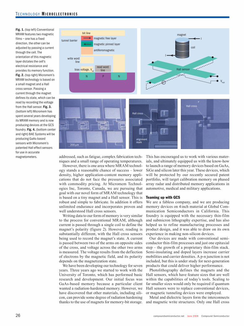
compoundsemiconductor.net June 2008 Compound Semiconductor26
Technology M i c r o e l e c t r o n i c s
addressed, such as fatigue, complex fabrication tech-niques and a small range of operating temperatures.
However, there is one area where MRAM technol-ogy stands a reasonable chance of success – lower density, higher application-content memory appli-cations that do not face the pressures associated with commodity pricing. At Micromem Technol-ogies Inc, Toronto, Canada, we are pursuing that goal with our novel form of MRAM technology that is based on a tiny magnet and a Hall sensor. This is robust and simple to fabricate. In addition it offers unlimited endurance and incorporates proven and well understood Hall cross sensors.
Writing data to our form of memory is very sim ilar to the process for conventional MRAM, although current is passed through a single coil to define the magnet’s polarity (figure 2). However, reading is substantially different, with the Hall cross sensors being used to record the magnet’s state. A current is passed between two of the arms on opposite sides of the cross, and voltage across the other two arms is measured. The voltage results from the deflection of electrons by the magnetic field, and its polarity depends on the magnetization state.
We have been developing our technology for seven years. Three years ago we started to work with the University of Toronto, which has performed basic research and development. Our initial focus was GaAs-based memory because a particular client wanted a radiation-hardened memory. However, we have discovered that other mater ials, including sili-con, can provide some degree of radiation hardening thanks to the use of magnets for memory-bit storage.
This has encouraged us to work with various mater-ials, and ultimately equipped us with the know-how to launch a range of memory devices based on GaAs, SiGe and silicon later this year. These devices, which will be protected by our recently secured patent portfolio, will target calibration memory on phased array radar and distributed memory applications in automotive, medical and military applications.
Teaming up with GCSWe are a fabless company, and we are producing memory devices on 4 inch material at Global Com-munication Semiconductors in California. This foundry is equipped with the necessary thin-film and submicron lithography expertise, and has also helped us to refine manufacturing processes and product design, and it was able to draw on its own experience in making non-silicon devices.
Our devices are made with conventional semi-conductor thin-film processes and just one epitaxial step – the growth of a proprietary thin-film stack. Semi-insulating and doped layers increase carrier mobilities and carrier densities. A p-n junction is not included, but this is under study for next-generation products that could deliver higher performance.
Photolithography defines the magnets and the Hall sensors, which have feature sizes that are well within the capabilities of today’s tools. Scaling to far smaller sizes would only be required if quantum Hall sensors were to replace conventional devices, or magnetic tunneling devices were employed.
Metal and dielectric layers form the interconnects and magnetic write structures. Only one Hall cross
bit line
magnetic free layer
magnetic pinned layertunnel barrier
antiferromagnetic
write wordline
bias voltage, Vdd
read wordline
N NPVHall
Hall sensor
coil
magnetI
I
Fig. 1. (top left) Conventional MRAM features two magnetic films – one has a fixed direction, the other can be adjusted by passing a current through the cell. The orientation of this magnetic layer dictates the cell’s electrical resistance and provides its memory function. Fig. 2. (top right) Micromem’s MRAM technology is based on a small magnet and a Hall cross sensor. Passing a current through the magnet defines its state, which can be read by recording the voltage from the Hall sensor. Fig. 3. (bottom left) Micromem has spent several years developing its MRAM memory and is now producing devices at the GCS foundry. Fig. 4. (bottom center and right) BAE Systems will be producing GaAs-based sensors with Micromem’s patented Hall effect sensors for use in accurate magnetometers.
200 μm
alignment mark
Hall cross
Hall cross
CSJun08MICROMEM25-27.indd 26 20/5/08 14:14:10

Compound Semiconductor June 2008 compoundsemiconductor.net 27
Technology M i c r o e l e c t r o n i c s
sensor is required per bit as non-volatile bit storage only occurs in the ferromagnetic structural element.
Packaging follows, which employs a minimized and controlled ferromagnetic environment and cop-per lead frames. Bespoke designs can address spe-cific applications. For example, a magnetic shield can be incorporated into ferromagnetic non-volatile RAMs, and packages that are devoid of ferrous materials can be used in stand-alone Hall sensors. These can be hermetically sealed or placed in low-cost packages, depending on the customer’s needs.
Our stand-alone Hall sensors (figure 4) combine very low operating powers with a high sensitivity of more than 2.2 V/Tesla. This makes them candidates for defense applications, healthcare, mining, min-eral exploration, manu facturing and quality con-trol, and the automotive industry. They have many applications, inclu ding in situ material analysis of mining sample plugs. The device can take a “mag-netic” picture of the core sample and detect mineral constituents through pattern recognition.
We have recently teamed up with BAE Systems, which is planning to manufacture nanosensors with our patented technology at its Nashua, NH, foundry. Over the next few months, devices will be built for use in accurate magnetometers for military equipment.
Extending our GaAs-based MRAM technology to SiGe and silicon has bolstered our chances of ma king an impact in computer memory. However, we still face competition from three other approaches that promise to advance silicon’s memory capabilit-ies. Two of these alternatives are cell-to-cell optical interconnects and forms of wafer-scale technology that feature built-in tolerances to combat low yields.
The other threat is niobium rapid single flux quan-tum superconductive technology – an unpopular technology, but one that could deliver significant power benefits at higher clock speeds.
All of these options promise to increase circuit current density through advanced packaging tech-nologies, such as three-dimensional structures. Managing heat extraction will hold the key to building reliable circuits, and all of the technologies described have the potential to do this.
Where our technology could have the edge is in optical computing, thanks to GaAs MRAM devices’ compatibility with GaAs circuits that use optical logic and optical memory. Although optical com-puting has been touted as tomorrow’s technology since the mid-1980s, some recent work on nonlinear optical technology shows genuine promise. Hybrid MRAM is also possible, although magnetic storage is expected to outperform its optical equivalent in terms of density and speed.
All four technologies will have to progress to stand a chance of making an impact on the memory market. In optical devices, the switch offers the big-gest challenge. This is needed for logic and store functions, and significant advances in nonlinear optics are required to produce pure optical-to- optical devices. But the real challenge here, which is essential if these devices are to enter the mainstream market, is competitiveness with silicon in terms of performance, power, density and reliability. This is not going to be easy, but success would provide great rewards. We will continue to target this goal by developing our technology, while enjoying suc-cess through lucrative Hall sensor sales. l
MRAM is competing with three other types of non-volatile memory to provide a universal solution: phase-change RAM; ferroelectric RAM; and carbon-nanotube RAM. Descriptions of all of these technologies and details of their various strengths and weaknesses are provided by iSuppli’s report Handicapping the Emerging Memory Technologies.
Phase-change RAM (a) features a chalcogenide layer within the die. Changing this material’s state produces the “zeros and ones” that form the memory. When the material is amorphous it is highly resistive, but when it is crystalline it has a low resistivity. An electrode can provide local heating to “write” the memory, which can take place in just a few nanoseconds. The “word line” is used to activate a row and each column can be accessed individually through “bit lines”.
Carbon-nanotube RAM (b) employs an array of electrodes that are separated by slightly higher, insulating interconnect layers. Current in the carbon nanotubes – which
are suspended from interconnects and hang above the electrodes by several nanometers – are used to define the ones and zeros that provide the memory function. Applying a voltage to an electrode causes sagging of a nanotube so that it touches the electrode
and passes a current.Ferroelectric RAM (c) features a thin film
of lead zirconate titanate (PZT), which forms arrays of capacitors. The electric dipoles within the PZT can be orientated by an external electric field, with the direction of these dipoles providing the ones and zeros. A transistor reads the cell by forcing it into a particular state. If the cell is forced into a new state, then the atoms are reorientated and they produce a brief current pulse. No current pulse occurs if the cell is unchanged by the transistor’s action.
Alternative non-volatile memories
word line
N NP
bit line ferroelectric
interconnects carbon nanotube ribbons
oxide layersupports
silicon wafer
electrode
wordline
wordline
N N N
polycrystallinechalcogenide
bit line
ground groundamorphous
chalcogenide
About the authorSteven Van Fleet ([email protected]) is a director of Micromem.
(a)
(b)
(c)
CSJun08MICROMEM25-27.indd 27 20/5/08 14:14:31

Grange Properties: 1 Grange City Hotel, London EC3; 2 Grange Holborn Hotel, London WC1; 3 Grange
White Hall Hotel, London WC1; 4 Grange Blooms Townhouse, London WC1; 5 The Buckingham, London
WC1; 6 The Portland, London WC1; 7 The Lancaster, London WC1; 8 The Clarendon, London WC1; 9 Grange
Fitzrovia Hotel, London W1; 10 Grange Langham Court Hotel, London W1; 11 Grange Rochester Hotel,
London SW1; 12 Grange Strathmore Hotel, London SW7; 13 Grange Bracknell Hotel, Bracknell
For any enquiries please call Grange Hotels Central Reservations:
Tel: +44 (0)20 7233 7888 Fax: +44 (0)20 7630 9897
email: [email protected]
www.grangehotels.com
GRANGE HOTELS
London's leading independent hotel group presentsan opportuniity to relax, work and play in some of the
very best located and luxurious properties in the capital
we've got London covered...
Untitled-7 1 20/5/08 11:26:34

Compound Semiconductor June 2008 compoundsemiconductor.net 29
Technology O p t O e l e c t r O n i c s
Finally the silicon folks might actually need us. The copper interconnects that they are using are running out of steam, and this is starting to obstruct their advances in interchip communication. It’s a weak-ness that’s even threatening to bump Moore’s law off course because the electrical input and output func-tions needed in tomorrow’s state-of-the-art micro-processors will dissipate more power and demand a greater share of a chip’s real estate. Even today data transfer is a complicated task. Loss, dispersion and cross-talk have to be addressed with predistortion and sophisticated pulse recovery techniques in the transmit and receive stages, respectively.
Against this background of increasing com-plexity, optical interconnection schemes look like a good bet for the future. This technology offers several key advantages over copper, such as lower signal delay, higher bandwidth, reduced power con-sumption and freedom from electromagnetic inter-ference. In addition, it has the potential to deliver intrachip communication.
However, optical interconnects will only offer a practical solution if improvements are made to devices and interface systems. Copper is a viable solution at speeds of up to 10 Gbit/s, so data rates must be at least 20 Gbit/s for optoelectronics to be considered an option. Low power consumption is another prerequisite, alongside the ability to be integrated with silicon electronics. But there is no point in trying to meet any of these goals unless the emitters and detectors can be manufactured in large volumes with high yields.
At the University of California, Santa Barbara (UCSB), we are working on a device that could be the key component in chip-to-chip optical intercon-nects – a miniature, high-speed, efficient VCSEL. It has evolved out of our part of the US Defense Advanced Research Projects Agency’s chip-to-chip optical interconnects program, which also supports IBM’s “Terabus” project. It aims to demonstrate complete optical links between chips using poly-mer waveguides (figure 1). It’s a technology that’s competing with silicon photonics, but which offers lower power dissipation – the primary limiter for
continued scaling of processor speed.There are several benefits that VCSELs offer over
their edge-emitting cousins for optical interconnect applications: they are smaller; they are easier to fab-ricate in arrays; they support on-wafer testing; they offer high-speed operation at lower power consump-tion; and they are cheaper. However, many of the VCSELs that have been designed for optical inter-connects have large diameter apertures – typically
The copper interconnects that route chip-to-chip data transfer are starting to reach their speed limit. But this looming bottleneck can be overcome by switching to ultra-fast VCSELs with tiny threshold currents, say Yu-Chia Chang and Larry Coldren from the University of California, Santa Barbara.
Ultra-fast VCSELs promise to turbocharge chip communication
transmitter array
clock
receiver array
drivers decision circuits
Si-IC Si-IC
n-pad metal
oxide aperture
n-contact
p-contact
deep oxidationlayers
p-pad metal
BCB
active region
semi-insulating GaAs substrateAR coating
Fig. 1. (top) UCSB’s VCSEL could be used to form an array of transmitters that provide chip-to-chip interconnects. Fig. 2. (bottom) The UCSB InGaAs/GaAs quantum-well design features a blunter tapered aperture that enables very high modulation speeds at acceptable optical losses.
CSJun08UCSB29-31.indd 29 20/5/08 14:09:10

compoundsemiconductor.net June 2008 Compound Semiconductor30
Technology O p t O e l e c t r O n i c s
5–8 µm – that drive up the bias current required for a high modulation bandwidth. We avoid this pitfall by scaling down the VCSEL size. Although this leads to a power drop of 50%, it cuts power dissipa-tion and increases the bandwidth, while maintain-ing acceptable optical losses.
The devices that we have made are 980 nm bottom-emitting VCSELs with a tapered oxide aper-ture and a contact inserted within the n-type cavity (figure 2, p29). The standard emission wavelength of 850 nm was not selected because the strained InGaAs/GaAs quantum wells (QWs) that produce 980 nm emission deliver a higher intrinsic modula-tion bandwidth thanks to higher gain at lower car-rier densities. Some studies suggest that InGaAs QW-lasers are more reliable. But more importantly, this particular design is compatible with bottom-emission thanks to GaAs’ transparency at 980 nm.
Bottom emission means that flip-chip bonding can be used to integrate our VCSELs with elec-tronics. This eliminates wire bond inductance and the need for wire bonding. Backside microlenses can be added to collimate the output beam, which improves alignment tolerance and cuts packaging costs. This combination of advantages should equip our devices with the compatibility required for advanced computer and processor interconnection architectures and other datacom applications.
Our VCSEL’s key feature compared with prior art is a blunter tapered aperture and a larger oxide thick-ness next to the active region (figure 3). This provides a high degree of optical confinement and enables our laser to combine high speeds with acceptable optical losses. Employing a longer tapered section would reduce optical losses even further, but this results in larger mode volumes with an unacceptable penalty of much slower modulation speeds.
The parasitic capacitance of a relatively thin oxide aperture can restrict the modulation bandwidth of oxide-confined VCSELs. The capacitance is often reduced by proton implantation, which creates a thick, highly resistive region. However, this highly effective method requires additional process steps that threaten reliability, and increase fabrication costs and parasitic resistance.
We get around this problem by creating additional deep oxidation layers above the confining aperture, which lower the parasitic capacitance. By increas-ing the aluminum fraction of the AlGaAs layers in
the first several periods of the top distributed Bragg reflector, we can simultaneously form deep oxida-tion layers along with the oxide aperture.
It is easy to incorporate this simple approach into oxide-confined VCSELs with semiconductor mir-rors. No modifications to the fabrication techniques are required, and it increases the refractive index contrast in the unoxidized region where optical modes exist, thanks to the layers with higher alu-minum content. This means that mode volume is cut because the longitudinal mode is more confined. On top of this, reductions in parasitic resistance are delivered with minimal impact to optical loss, thanks to high-quality engineering of the band-structure and the p-doping profiles in the top mirror.
Our approach to VCSEL fabrication is compatible with existing manufacturing processes and begins with MBE growth of the epitaxial structure on semi-insulating (100) GaAs substrates (see figure 4 for an overview). Etching creates cylindrical mesas that expose the n-GaAs contact layer, before wet oxidation forms oxide apertures and deep oxidation layers. Metal evaporation adds the p-type Ti/Pt/Au and n-type Au/Ge/Ni/Au contacts.
Pad capacitance is reduced by removing the part of the n-GaAs contact layer (RF-ground) that lies beneath the p-pad metal (RF-signal). The low dielectric constant resin benzocyclobutene is inserted in its place before vias are opened to expose the contacts and Ti/Au is deposited for the pad metals. Finally, an anti-reflection coating is
“This device’s bandwidth makes it the fastest ever 980 nm VCSEL.”
(a) (b)
(c) (d)
(e) (f)
(g) (h)
Fig. 3. (right) This cross-sectional scanning electron image reveals key features in the UCSB VCSEL – five deep oxidation layers and a tapered oxide aperture. Fig. 4. (far right) UCSB’s high-speed VCSELs are fabricated with the following process steps: (a) mesa etch, (b) oxidation, (c) n-metal deposition, (d) p-metal deposition, (e) n-contact removal, (f) patterning with a low-dielectric resin, (g) pad metal deposition, and (h) adding an anti-reflection coating.
blunt-tapered section1 µm
CSJun08UCSB29-31.indd 30 20/5/08 14:09:33

Compound Semiconductor June 2008 compoundsemiconductor.net 31
Technology O p t O e l e c t r O n i c s
applied to reduce backside reflection.We have produced 3 µm diameter aperture
VCSELs with this process. These emitters have a slope efficiency of 0.67 W/A, which corresponds to a differential quantum efficiency of 54% (fig-ure 5). Threshold current is just 0.144 mA, which is comparatively low for high-speed VCSELs as they usually have threshold currents of at least 0.4 mA. Peak wall-plug efficiency is 31%, maximum output power is 3.1 mW and the threshold voltage is just 1.47 V – very low for such a small device as it is only 220 meV larger than the photon energy.
Small-signal modulation measurements on our 3 µm aperture emitter revealed that it could respond to frequencies beyond 20 GHz, the upper detection limit for our instrument (figure 4). This device’s bandwidth clearly exceeds that frequency, which makes it the fastest ever 980 nm VCSEL.
We evaluated this device’s suitability for real-world systems with large-signal digital modula-tion experiments. At 20 ºC and a modulation rate of 35 Gbit/s, our 3 µm diameter device produced bit error rates as low as 10–11 over a couple of meters of fiber, which demonstrates that it is suitable for high-quality interchip communication. The VCSEL
power dissipation, excluding RF circuitry, is only 10 mW, which corresponds to the highest data rate/power-dissipation ratio that has ever been obtained for any type of laser source.
We are now targeting data rates of 40 Gbit/s, which can be reached by simply extending our existing techniques. However, we are also engaged in another project that has the potential to get us to the 100 Gbit/s range with a single channel. If such high speeds could be achieved, then this will further enhance the attractiveness of employing VCSELs for chip-to-chip interconnects. l
Further readingT Anan 2007 Proc. International Symposium on VCSELs and Integrated Photonics E3.Y-C Chang et al. 2006 Electron. Lett. 42 1281.Y-C Chang et al. 2007 Electron. Lett. 43 1022.E Hegblom et al. 1997 IEEE J. Select. Topics Quantum Electron. 3 379.A A L-Omari et al. 2004 IEEE Photon. Technol. Lett. 16 969.L Schares et al. 2006 IEEE J. Sel. Topics Quantum Electron. 12 1032.E Strzelecka et al. 1995 Electron. Lett. 31 724.
4.0
3.5
3.0
2.5
2.0
1.5
1.0
0.5
0.00 1 2 3 4 5 6 7 8
current (mA)
volta
ge (V
)4.0
3.5
3.0
2.5
2.0
1.5
1.0
0.5
0.03 µm device @ 20°C
outp
ut p
ower
(mW
)
100
75
50
25
0
tem
pera
ture
rise
(°C)
voltageoutput powertemperature rise
18
0 5 10 15 20
0.3512
6
0
–6
–12
–18
frequency (GHz)
frequ
ency
resp
onse
(dB)
0.7
1.0
1.75
3.0
4.4
–3
–4
–5
–6
–7
–8
–9
–10–11
–11
log 10
(BER
)
–10 –9received power (dBm)
–8 –7 –6 –5 –4
35 Gbit/s @ 20°C
Ibias = 4.4 mA
Vac = ~0.84 Vpp
About the authorsLarry Coldren (left) is the Fred Kavli professor of optoelectronics and sensors at UCSB, and the director of the university’s Optoelectronics Technology Center. He joined UCSB in 1984 after spending 13 years as a researcher at Bell Laboratories. Yu-Chia Chang (right) is a PhD student in the electrical and computer engineering department at UCSB. His research interests include the design, growth and characterization of high-speed VCSELs.
Fig. 5. (top left) UCSB’s 3 µm diameter aperture VCSELs deliver up to 3 mW at 20 °C. This laser has a series resistance of approximately 250 Ω at 4.4 mA bias current, the conditions that are used for the large signal experiments. Thermal impedance is 3.3 °C/mW and the temperature rise is 33 °C at this current, but improvements may be possible through refinements in the design of the VCSELs. Fig. 6. (top right) Adjustments in bias current from 0.35–4.4 mA alter the modulation speed of the 3 µm diameter device, which is highest at 4.4 mA. At this bias the modulation exceeds 20 GHz, which is a record for 980 nm VCSELs. Fig. 7. (left) Bit error rates (BERs) were measured for UCSB’s 35 Gbit/s, 3 µm diameter device at 20 °C. This VCSEL was biased at 4.4 mA and a peak-to-peak voltage swing of 0.84 V was used. The input was a non-return-to-zero signal with 27–1 word length. Eye diagrams are shown in the inset figure, which reveal that the eye is clearly open. The extinction ratio is 5.4 dB. In the BER curve, a variable optical attenuator (VOA) was used to take all but the lowest data point. Poor detector responsivity and a 3 dB insertion loss of the VOA prevented the measurement of BERs between 10–4 and 10–7. To ensure measurement accuracy, the lowest data point was gated for 30 minutes with a total of 583 errors.
CSJun08UCSB29-31.indd 31 20/5/08 14:09:55

compoundsemiconductor.net June 2008 Compound Semiconductor32
Technology R e s e a R c h R e v i e w
P h o t o v o lta i c s
Electroluminescence exposes subcellsGerman researchers have developed the first technique that measures the electrical char-acteristics of the three solar cells that make up triple-junction devices deployed in satel-lites and concentrator photovoltaics.
The technique promises to improve conver-sion efficiency and can reveal current–voltage curves for each cell from calculations based on electroluminescence (EL) data.
The team has already produced current density–voltage curves and external quan-tum efficiencies for all three cells when it probed a GaInP/GaInAs/Ge device with EL measurements spanning 0.6–1.8 µm.
The researchers uncovered values for the radiative limit – the current–voltage curve for a solar cell free from non- radiative
recombination current. “It constitutes an upper limit for efficiency and open-circuit voltage if radiative recombination is the dom-inant recombination process,” said Thomas Kirchartz from the photovoltaics department at the Research Center, Jülich, Germany.
According to him, non-radiative and radiative recombination can be determined through comparisons of the radiative open-circuit voltage and the measured open-circuit voltage. “Together with the internal voltages calculated from the electroluminescence, we can assess the quality of the subcells in terms of recombination current, while the quantum efficiency evaluates the subcells in terms of the photocurrent,” said Kirchartz.
It takes 5–10 minutes to perform an EL scan
and 1–2 hours to determine the internal volt-age at several injection currents. “Data inter-pretation is done automatically with a Matlab script in a short time,” said Kirchartz.
Future work at Jülich and Stuttgart is focusing on improving the experimental set-up through better infrared detectors and the addition of a double monochromator that eliminates more stray light.
An EL measurement tool capable of quick feedback will be set up at Fraunhofer ISE in Freiberg and will be used for improving triple-junction solar cell performance.
P r o c E s s i n g
s u b s t r at E s
GaAs-based InGaAs lasers can now hit the key telecom wavelength of 1.3 µm, thanks to the combined efforts of the Chinese Acad-emy of Sciences and Chalmers University of Technology, Sweden.
This partnership’s edge-emitting design delivers several benefits over commercial InP-based lasers that are deployed in today’s networks. These include cheaper substrates, stronger carrier confinement and higher thermal conductivity, which could enable uncooled device operation.
A metamorphic buffer and a subsequent layer with 7% less indium provided a plat-form for the growth of an In0.47GaAs single quantum well that lased at 1337 nm.
The researchers’ MBE-grown graded-
index separate-confinement heterostructure has a 1200 µm cavity, a 20 µm stripe width and a threshold current of just 205 kA/cm2.
“Rapid annealing is the key step to our low threshold currents,” explained Zhichuan Niu from the Chinese Academy of Sciences. Annealing the epiwafer for 10 s at 850 °C removed the dislocations in the structure, according to transmission electron micro-scopy images of similar designs with the same metamorphic buffer.
“Our laser is not designed for high output power, and the maximum [continuous-wave] output is around 10 mW,” explained Niu.
The researchers are hoping to team up with a laser manufacturer and are looking to improve device performance. They want to extend emission to 1.55 µm – the key wave-length for telecom lasers.
Free-standing AlN can be produced by “self-separation”, according to resear chers at Tokyo University of Agriculture and Technology, and Tokuyama Corporation – a Japan ese manufacturer of chemicals, plas-tics and electronic materials.
This technique, which causes an AlN film to separate from its sapphire substrate as it cools to room temperature, promises to deliver a relatively simple method for the production of AlN substrates. These substrates could be used as a platform for
deep- ultraviolet LEDs and high-power, high-frequency electronic devices.
The Japanese partnership makes its free-standing material by first growing a 100 nm thick layer of AlN on sapphire by HVPE at 1065 °C. Hydrogen gas reaches the interface through diffusion and reacts with sapphire to form voids with a depth of 50 nm. An 85 µm thick AlN layer is then grown on this struc-ture, before cooling causes the AlN to sep-arate from the sapphire.
This approach delivers several advant-ages over HVPE growth of a thick AlN film directly onto sapphire, which tends to crack during cooling due to differences in the
thermal expansion coefficients of the two materials. In this case, separating sapphire and AlN is difficult because sapphire is very hard and no practical etchant exists.
The researchers say that the surface of their AlN is “quite smooth” and free from cracks. Transmission electron microscopy images suggest a dislocation density on the top surface of 1.l × 109 cm–2, and opti-cal meas urements reveal a transparency for wavelengths of more than 208 nm.
InGaAs laser breaks into telecom territory
Voids aid AlN formation
Journal referenceD Wu et al. 2008 Elec. Lett. 44 474.
Journal referenceY Kumagai et al. 2008 Appl. Phys. Express 1 045003.
Journal referenceT Kirchartz et al. 2008 Appl. Phys. Lett. 92 123502.
Annealing removes the dislocations in InGaAs epiwafers with a metamorphic buffer, according to transmission electron microscopy studies.
active layers
p-InAlGaAs
n-InAlGaAs
graded n-InGaAs
3 nm GaAs
CSJun08ResearchReview32.indd 32 20/5/08 14:08:03

SAFC Hitech is the new face that’s set to transform the materials technology sector.
It sees Epichem, the proven market leader with a 25 year pedigree supplying the compound semiconductor industry, joining forces with the strength of SAFC®. Bringing you a reliable and responsive partner who is now even more prepared to deliver the innovative chemistry and extensive supply chain expertise you need, when and where you need it.
SAFC Hitech offers a global manufacturing and regional support infrastructure that is essential to enable technology and make your ideas happen.
The future of materials technology is revealed. Look to SAFC Hitech and email us for further details at [email protected]
SAFC Hitech™ Changing the face of materials technology
www.safchitech.com
3170-22 Hitech Compound ad Compo1 1 20/5/08 13:06:57